1
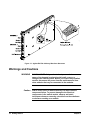
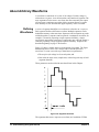
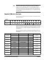
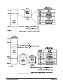
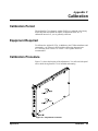
Agilent TS-5400 Functional Test System Series IIB Agilent E6173A Arbitrary Waveform Generator User’s Manual *E6173-90021* Manual Part Number E6173-90021 Agilent Technologies Notices © Agilent Technologies, Inc. 1996 - 2003 Manual Part Number No part of this manual may be reproduced in any form or by any means (including electronic storage and retrieval or translation into a foreign language) without prior agreement and written consent from Agilent Technologies, Inc. as governed by United States and international copyright laws. E6173-90021 Documentation History The material contained in this document is provided “as is,” and is subject to being changed, without notice, in future editions. Further, to the maximum extent permitted by applicable law, Agilent disclaims all warranties, either express or implied, with regard to this manual and any information contained herein, including but not limited to the implied warranties of merchantability and fitness for a particular purpose. Agilent shall not be liable for errors or for incidental or consequential damages in connection with the furnishing, use, or performance of this document or of any information contained herein. Should Agilent and the user have a separate written agreement with warranty terms covering the material in this document that conflict with these terms, the warranty terms in the separate agreement shall control. All Editions and Updates of this manual and their creation date are listed below. The first Edition of the manual is Edition 1. The Edition number increments by 1 whenever the manual is revised. Updates, which are issued between Editions, contain replacement pages to correct or add additional information to the current Edition of the manual. Whenever a new Edition is created, it will contain all of the Update information for the previous Edition. Each new Edition or Update also includes a revised copy of this documentation history page. Edition 1 (E6173-90000)Februaryl 1996 Edition 2 (E6173-90001)May 1996 Edition 3 (E6173-90011)September 2000 Edition 4 (E6173-90021) August 2003 Printed in USA Agilent Technologies, Inc. 1601 California Street Palo Alto, CA 94304 USA Warranty Technology Licenses The hardware and/or software described in this document are furnished under a license and may be used or copied only in accordance with the terms of such license. Restricted Rights Legend If software is for use in the performance of a U.S. Government prime contract or subcontract, Software is delivered and licensed as “Commercial computer software” as defined in DFAR 252.227-7014 (June 1995), or as a “commercial item” as defined in FAR 2.101(a) or as “Restricted computer software” as defined in FAR 52.227-19 (June 1987) or any equivalent agency regulation or contract clause. Use, duplication or disclosure of Software is subject to Agilent Technologies’ standard commercial license terms, and non-DOD Departments and Agencies of the U.S. Government will receive no greater than Restricted Rights as defined in FAR 52.227-19(c)(1-2) (June 1987). U.S. Government users will receive no greater than Limited Rights as defined in FAR 52.227-14 (June 1987) or DFAR 252.227-7015 (b)(2) (November 1995), as applicable in any technical data. Safety Notices C auti on A Caution notice denotes a hazard. It calls attention to an operating procedure, practice, or the like that, if not correctly performed or adhered to, could result in damage to the product or loss of important data. Do not proceed beyond a Caution notice until the indicated conditions are fully understood and met. WA RN ING A WARNING notice denotes a hazard. It calls attention to an operating procedure, practice, or the like that, if not correctly performed or adhered to, could result in personal injury or death. Do not proceed beyond a WARNING notice until the indicated conditions are fully understood and met. Safety Summary The following general safety precautions must be observed during all phases of operation of this system. Failure to comply with these precautions or with specific warnings elsewhere in this manual violates safety standards of design, manufacture, and intended use of the system. Agilent Technologies, Inc. assumes no liability for the customer's failure to comply with these requirements. WARNING: DO NOT REMOVE ANY SYSTEM COVER Operating personnel must not remove system covers. Component replacement and internal adjustments must be made only by qualified service personnel. Equipment that appears damaged or defective should be made inoperative and secured against unintended operation until they can be repaired by qualified service personnel. General This product is provided with a protective earth terminal. The protective features of this product may be impaired if it is used in a manner not specified in the operation instructions. Environmental Conditions Unless otherwise noted in the specifications, this system is intended for indoor use in an installation category II, pollution degree 2 environment. It is designed to operate at a maximum relative humidity of 80% and at altitudes of up to 2000 meters. Refer to the specifications tables for the ac mains voltage requirements and ambient operating temperature range. WARNING: DO NOT OPERATE IN AN EXPLOSIVE ATMOSPHERE Do not operate the system in the presence of flammable gases or flames. If the equipment in this system is used in a manner not specified by Agilent Technologies, the protection provided by the equipment may be impaired. Before applying power Verify that all safety precautions are taken. Note the external markings described in “Safety Symbols and Regulatory Markings” on page 4. Cleaning Instructions Clean the system cabinet using a soft cloth dampened in water. Safety and Support Information 3 Ground the System To minimize shock hazard, the system chassis must have a hard-wired connection to an electrical protective earth ground. The system must also be connected to the ac power mains through a power cable that includes a protective earth conductor. The power cable ground wire must be connected to an electrical ground (safety ground) at the power outlet. Any interruption of the protective grounding will cause a potential shock hazard that could result in personal injury. Fuses Use only fuses with the required rated current, voltage, and specified type (normal blow, time delay). Do not use repaired fuses or short-circuited fuse holders. To do so could cause a shock or fire hazard. Operator Safety Information MODULE CONNECTORS AND TEST SIGNAL CABLES CONNECTED TO THEM CANNOT BE OPERATOR ACCESSIBLE: Cables and connectors are considered inaccessible if a tool (e.g., screwdriver, wrench, socket, etc.) or a key (equipment in a locked cabinet) is required to gain access to them. Additionally, the operator cannot have access to a conductive surface connected to any cable conductor (High, Low or Guard). 4 Safety and Support Information ASSURE THE EQUIPMENT UNDER TEST HAS ADEQUATE INSULATION BETWEEN THE CABLE CONNECTIONS AND ANY OPERATOR-ACCESSIBLE PARTS (DOORS, COVERS, PANELS, SHIELDS, CASES, CABINETS, ETC.): Verify there are multiple and sufficient protective means (rated for the voltages you are applying) to assure the operator will NOT come into contact with any energized conductor even if one of the protective means fails to work as intended. For example, the inner side of a case, cabinet, door, cover or panel can be covered with an insulating material as well as routing the test cables to the module’s front panel connectors through non-conductive, flexible conduit such as that used in electrical power distribution. Safety Symbols and Regulatory Markings Symbols and markings on the system, in manuals and on instruments alert you to potential risks, provide information about conditions, and comply with international regulations. Table 1 defines the symbols and markings you may encounter. Table 1 Safety Symbols and Markings Safety symbols Warning: risk of electric shock. Caution: refer to accompanying documents. Alternating current. Both direct and alternating current. Earth (ground) terminal Protective earth (ground) terminal Frame or chassis terminal Terminal is at earth potential. Used for measurement and control circuits designed to be operated with one terminal at earth potential. Switch setting indicator. O = Off, | = On. Standby (supply); units with this symbol are not completely disconnected from ac mains when this switch is off. To completely disconnect the unit from ac mains, either disconnect the power cord, or have a qualified electrician install an external switch. Regulatory Markings The CE mark is a registered trademark of the European Community. The CSA mark is a registered trademark of the Canadian Standards Association. N10149 ISM 1-A The C-tick mark is a registered trademark of the Spectrum Management Agency of Australia. This signifies compliance with the Australian EMC Framework regulations under the terms of the Radio Communications Act of 1992. This text indicates that the product is an Industrial Scientific and Medical Group 1 Class A product (CISPR 11, Clause 4). Safety and Support Information 5 Service and Support Any adjustment, maintenance, or repair of this product must be performed by qualified personnel. Contact your customer engineer through your local Agilent Technologies Service Center. http://www.agilent.com Click the link to Test & Measurement. Select your country from the drop-down menus. The Web page that appears next has contact information specific for your country. Agilent on the Web You can find information about technical and professional services, product support, and equipment repair and service on the Web: Table 2 6 Agilent by Phone If you do not have access to the Internet, call one of the numbers in Table 2. Agilent Call Centers and Regional Headquarters United States and Canada: Test and Measurement Call Center (800) 452 4844 (toll-free in US) Europe: (41 22) 780 8111 Japan: Measurement Assistance Center (81) 0426 56 7832 Latin America: 305 269 7548 Asia-Pacific: (85 22) 599 7777 Safety and Support Information Contents Chapter 1 Getting Started ............................................................................................................... 9 Using this Chapter ........................................................................................................ 9 Description.................................................................................................................... 9 Warnings and Cautions ............................................................................................... 10 Setting the Address Switch ......................................................................................... 11 Setting the Interrupt Line ............................................................................................ 11 Installing in a VXI Mainframe.................................................................................... 12 Chapter 2 Understanding the Agilent E6173A ........................................................................... 13 Using this Chapter ...................................................................................................... 13 Block Diagram ............................................................................................................ 13 About Arbitrary Waveforms ....................................................................................... 14 Defining Waveforms ........................................................................................... 14 Sample Rate ......................................................................................................... 15 Segments ............................................................................................................. 15 Sequences ............................................................................................................ 16 Defining Segments and Sequences ............................................................................. 18 Segment Value .................................................................................................... 18 Sequences ............................................................................................................ 19 Markers ................................................................................................................ 19 Segment Memory Example ........................................................................................ 20 Chapter 3 Programming the Agilent E6173 ................................................................................ 23 Using this Chapter ...................................................................................................... 23 A16 and A24 Memory ................................................................................................ 23 Waveform Memory ............................................................................................. 24 Sequence Memory Registers ...................................................................................... 25 Segment Memory Pointer .................................................................................... 25 Repeat Count ....................................................................................................... 25 Dwell Count ........................................................................................................ 26 Next Sequence Pointer ........................................................................................ 26 General Programming Information............................................................................. 26 Sequence Operation ............................................................................................. 26 Channel Selection ................................................................................................ 26 A24 Access .......................................................................................................... 27 Memory Load/Run .............................................................................................. 27 EOS and Stop Control Bits ................................................................................................. 27 Trigger Operation ................................................................................................ 28 Contents 7 Immediate Jump Operation (On the Fly) ......................................................................................................... 28 Abort Operation ................................................................................................... 29 Starting the Agilent E6173 ..................................................................................................... 29 Examples..................................................................................................................... 30 Single Sequence .................................................................................................. 30 Multiple Sequences ............................................................................................. 30 Appendix A Specifications ................................................................................................................ 33 Appendix B Register Definitions ..................................................................................................... 35 Using this Appendix ................................................................................................... 35 Addressing the Registers ............................................................................................ 35 The Base Address ................................................................................................ 35 Register Offset ..................................................................................................... 37 Control Register Descriptions..................................................................................... 38 Manufacturer Identification Register .................................................................. 38 Device Type Register .......................................................................................... 38 Card Status/Control Register ............................................................................... 38 Offset Register ..................................................................................................... 40 Channel Status Register ...................................................................................... 40 Channel Trigger Register .................................................................................... 41 Clock Adjust Register ......................................................................................... 42 On the Fly Register ............................................................................................. 43 A24 Registers.............................................................................................................. 44 Waveform Memory ............................................................................................ 44 Segment Memory ................................................................................................ 44 Segment Pointer .................................................................................................. 44 Repeat Counter Memory ..................................................................................... 44 Dwell Counter Memory ...................................................................................... 44 Next Sequence Pointer ........................................................................................ 44 Appendix C Calibration .................................................................................................................... 45 Calibration Period ....................................................................................................... 45 Equipment Required ................................................................................................... 45 Calibration Procedure ................................................................................................. 45 Procedure: ............................................................................................................ 46 Index ................................................................................................................................ 49 8 Contents Chapter 1 Getting Started Using this Chapter This chapter describes the Agilent E6173A (formerly Agilent Z2471A) Arbitrary Waveform Generator module. This chapter contains the following sections: • Description . . . . . . . . . . . . . . . . . . . . . . . . . . . . . . . . . . . . . . • Warnings and Cautions . . . . . . . . . . . . . . . . . . . . . . . . . . . . . • Setting the Address Switch . . . . . . . . . . . . . . . . . . . . . . . . . . • Setting the Interrupt Line . . . . . . . . . . . . . . . . . . . . . . . . . . . • Installing in a VXI Mainframe . . . . . . . . . . . . . . . . . . . . . . . page 9 page 10 page 11 page 11 page 12 Description The Agilent E6173A is a register-based, two channel, isolated arbitrary waveform generator. Each independent channel provides a waveform output, a marker output, and an input trigger BNC connector. Additionally, a BNC connector is provided to allow the use of an external timebase (the external timebase is common to both channels). The Agilent E6173A Arbitrary Waveform Generator is shown in Figure 1-1. The module is controlled via register access in A24 VXIbus addressing. Multiple waveforms can be downloaded into memory. Waveforms can be sequenced in any order, linked to other waveforms, and repeated. The sample rate can be set by the internal 10 MHz timebase or by using an external timebase. A programmable marker output on each channel can be used to synchronize other instruments. Each channel also accepts an external trigger input to allow both channels or multiple modules to start simultaneously. Chapter 1 Getting Started 9 Figure 1-1. Agilent E6173A Arbitrary Waveform Generator Warnings and Cautions 10 WARNING SHOCK HAZARD. Only service-trained personnel who are aware of the hazards involved should install, remove, or configure the switch module. Before you remove any installed module, disconnect AC power from the mainframe and from other modules that may be connected to the modules. Caution STATIC ELECTRICITY. Static electricity is a major cause of component failure. To prevent damage to the electrical components in the switch module, observe anti-static techniques whenever removing a module from the mainframe or whenever working on a module. Getting Started Chapter 1 Setting the Address Switch The logical address switch (LADDR) factory setting is 80. You may have to change the setting during module installation. Valid address values are from 1 to 255. If the Arbitrary Waveform Generator is used with an Agilent E1405B or E1406A Command Module in a C Size Mainframe, refer to the “Agilent Command Module User's Guide” for addressing information. Figure 1-1 shows the switch location and factory setting. Note The value set on the address switch should be an integer multiple of 8 if the module is an instrument used in an Agilent E1405B or E1406A VXIbus mainframe. Setting the Interrupt Line The Arbitrary Waveform Generator can generate VXIbus interrupts. The interrupt is sent to, and acknowledged by, the Command Module (or other controller) via the VXIbus back plane interrupt lines. Different controllers treat the interrupt lines differently, and you should refer to your controller's documentation to determine how to set the interrupt line on your module. Refer to Figure 1-1 to change the interrupt line used by the module. If an interrupt is to be used, you should generally select a line other than 1. Level 0 disables the interrupt. The module's factory setting is 1. To change the setting, turn the rotary selector with a small flat-blade screwdriver. Chapter 1 Getting Started 11 Installing in a VXI Mainframe The Arbitrary Waveform Generator can be installed in any available mainframe slot except slot 0. Installation in an Agilent E1400B mainframe is shown below. Figure 1-2. Installing the Agilent E6173A 12 Getting Started Chapter 1 Chapter 2 Understanding the Agilent E6173A Using this Chapter This chapter contains information about the operation of the Arbitrary Function Generator. Specifically, this chapter contains: • Block Diagram . . . . . . . . . . . . . . . . . . . . . . . . . . . . . . . . . . . • About Arbitrary Waveforms . . . . . . . . . . . . . . . . . . . . . . . . . • Defining Segments and Sequences . . . . . . . . . . . . . . . . . . . . • Segment Memory Example. . . . . . . . . . . . . . . . . . . . . . . . . . page 13 page 14 page 18 page 20 Block Diagram Figure 2-1. Simplified Block Diagram Chapter 2 Understanding the Agilent E6173A 13 About Arbitrary Waveforms A waveform is created out of a series of dc voltages. Each dc voltage is referred to as a segment. A waveform can have any number of segments. The more segments used to create a waveform, the more accurately the output will represent a continuous waveform. More segments, however, require more memory to store and limit the upper frequency of the waveform. Defining Waveforms A series of segments that define a waveform are referred to as a sequence. Each sequence defines a different waveform. Multiple sequences can be loaded into memory at the same time. Sequences can be output in any order or linked together. A sequence can be repeated. A continuous waveform, for example, is created by repeating a single sequence infinitely, a single waveform is output when a sequence is output only once, and a dc output is created by repeating a single segment sequence infinitely. Sequences are described beginning on page 2-<Reference>. Figure 2-2 shows a simple sinewave created using 9 segments. The figure demonstrates how a series of dc voltages can be used to represent a waveform. To create a waveform you must know two parameters: • The step size (dc voltage level) at each point, and • How often the steps occur (sample rate) or how long each step is held (segment duration) These parameters are described in more detail later in this Chapter. Figure 2-2. Segment Sinewave The segments that create a sequence (waveform) are loaded into VXIbus 14 Understanding the Agilent E6173A Chapter 2 A24 memory. Multiple waveforms can be loaded at the same time and all segments are loaded into adjacent memory locations. The Agilent E6173A, when instructed to output, steps through these memory locations in ascending order. To send the correct waveform, the Agilent E6173A must know the starting segment memory location, and the ending segment memory location. Upon start-up, the Agilent E6173A determines the address of the first segment in a sequence by loading the segment pointer value stored in sequence memory. The first segment pointer value is 0 unless it has been modified by a write to the `On the Fly' register before starting the waveform. The first segment can be the first segment of an entire waveform or can be a `zero output' one-segment sequence. The last segment in a sequence is indicated by the use of a special bit (EOS) in the segment memory. The use of the segment and sequence memory is described in more detail later in this Chapter and in Chapter 3. Sample Rate The sample rate and segment duration are directly related as: n segmentduratio = ----------------------------samplerate The sample rate (or how often the output changes to the next segment value) can be set either internally or by the use of an external clock input. Sample rates can be set as: • Using Internal Clock: 2.00 µSec + (Clock Adjust Count) X 100E-9 Sec • Using External Clock: 20/(External Clock Frequency) + (Clock Adjust Count)/(External Clock Frequency) Note The Clock Adjust Count is set in the Clock Adjust Register. Refer to Appendix B for more information about this register. h a clock adjust count of 0, the minimum segment duration (or fastest sample rate) is 2.00 µSec (or 500 kHz). You can set the segment duration using the Clock Adjust Register, or you can set a dwell on each segment. A dwell instructs the Agilent E6173A to hold (or dwell) on each segment for a specified number of segment durations. You can set a dwell from 0 to 65535. For example, with a Clock Adjust Register value of 0, the minimum segment duration is 2.00 µSec. Setting the Dwell value to 1000 creates a segment duration of 2.002 mSec. Segments A waveform can contain any number of segments. Each segment defines an output dc voltage. The voltage output at a particular segment is determined as: Outputvoltage = Segmentvalue × StepSize In the Agilent E6173A, the minimum step value is 31.242370 µVolts (with Chapter 2 Understanding the Agilent E6173A 15 0dB attenuation). This minimum step value is derived by taking the full scale range ± 16.38 volts and dividing by the total number of steps: 220 = 1048576. Thus, the minimum step size is: (16.38 - (-16.38))/1048576 = 31.242370 µV Conversely, for a desired voltage, the segment value (DAC code) required is: Vdesired / 31.242370 µV This segment value is represented by a 20-bit, 2's complement binary word. The 9 segment sinewave (shown in Figure 2-2) could have the following values for each segment: Segment Number Sequences Segment Value X Step Size = Output Voltage 0 0 31.242. µVolts 0V 1 102870 31.242. µVolts 3.2 V 2 157606 31.242. µVolts 4.9 V 3 138597 31.242. µVolts 4.3 V 4 54737 31.242. µVolts 1.7 V 5 -54736 31.242. µVolts -1.7 V 6 -138597 31.242. µVolts -4.3 V 7 -157606 31.242. µVolts -4.9 V 8 -102880 31.242. µVolts -3.2 V The series of segments that define a waveform are called a sequence. Sequences can be added together to create complex waveforms. To use sequences you need to consider three parameters: • An end-of-sequence bit (to indicate the last segment in a sequence) • A sequence repeat value (to indicate how many times this sequence should be repeated) • A next sequence pointer (to show either which sequence to output next or where to stop). An End-of-Sequence bit indicates that the sequence is done (that is, all the segments have been output). When this bit is found, the Agilent E6173A can stop and hold the last voltage output (value of the last segment), can jump to another sequence in memory, or can repeat the last sequence any number of times. 16 Understanding the Agilent E6173A Chapter 2 Note If a sequence does not have a repeat value or a next sequence pointer, but does contain a stop bit, the output of the Agilent E6173A is left at the dc value of the last segment in the sequence. Every segment sequence MUST have an end of sequence bit. Every sequence has a next sequence pointer. If a segment does not have “EOS” set, segment memory will “roll-over” and the waveform sequence is repeated. If the segment does have the “EOS” set, but a valid next sequence address has not been stored, the Agilent E6173A may jump to a random address producing unpredictable results. Even if a repeat value is stored, the next sequence pointer must be stored or the next sequence pointer must contain the stop bit. Figure 2-3 shows an example ramp waveform output. The example is made up of three sequences: • Sequence A is a ramp of 6 segments. The segment dwell is set to 0 and the sequence repeat is set to 0. The next sequence pointer is set to point to the first segment in sequence B. • Sequence B is identical to sequence A except that segment dwell is set to 1 (each segment is held for two samples). The next sequence pointer is set to point to the first segment in sequence C. • Sequence C is a mirror image of sequence A. The segment dwell is set to 0 but the sequence repeat is set to 2 and so executes the sequence three times. The next sequence pointer is set to the first segment in sequence A. • All the sequences are then repeated indefinitely. Figure 2-3. Example Waveform Output Chapter 2 Understanding the Agilent E6173A 17 Defining Segments and Sequences Segments are defined with a 24-bit memory register, referred to a segment memory. The 24-bits must be put in VXIbus memory as two 16-bit word writes. The method used by the Agilent E6173A puts the 16 most significant bits in the n + 2 memory location, and the four least significant bits in the n + 0 memory location. To show this as two 16-bit registers, where n is the segment number: Address 15 base + (n + 2) 14 13 12 11 10 9 8 7 (MSB) 15 base + n 14 6 5 4 3 2 1 0 4 3 2 1 0 Segment Value 13 12 11 10 9 8 7 Not Used Segment Value 6 EOS MKR 5 Not Used Segment Value (LSB) The segment value is a 20-bit, 2's compliment value. For example, to set the output voltage to +5.00 Volts: Outputvoltage = Segmentvalue × StepSize Since, , then 5.00 Segmentvalue = ----------------------------= 160039 -4 × In 20-bit binary and hexadecimal form, the value 160039 looks like: Binary 19 18 17 16 15 14 13 12 11 10 9 8 7 6 5 4 3 2 1 0 0 0 1 0 0 1 1 1 0 0 0 1 0 0 1 0 0 1 1 1 Hex 2 7 1 2 7 Bit 19 is the sign bit for the 2's compliment number. When bit 19 is set, the number is a negative number. For example, to set the output voltage to -5.00 Volts: 20 – 5.00 SegmentValue = ------------------------------ + 2 = 888537 -4 0.3124 ×10 In 20-bit binary and hexadecimal form, the value 888537 looks like: Binary Hex 18 19 18 17 16 15 14 13 12 11 10 9 8 7 6 5 4 3 2 1 0 1 1 0 1 1 0 0 0 1 1 1 0 1 1 0 1 1 0 0 1 D 8 Understanding the Agilent E6173A E D 9 Chapter 2 Because the segment value is a 20-bit value, it must be broken into two 16-bit words in VXIbus memory. To do this, the four least significant bits are sent as the least significant bits of the first memory word. For example, the 20-bit +5.00 V value: 19 18 17 16 15 14 13 12 11 10 9 8 7 6 5 4 3 2 1 0 0 0 1 0 0 1 1 1 0 0 0 1 0 0 1 0 0 1 1 1 Binary Hex 2 7 1 2 7 is stored in the VXIbus memory as two 16-bit values: Address base +(n + 2) 15 14 0 0 13 12 11 10 1 0 0 1 2h base + n 9 8 7 6 1 1 0 0 7h 5 4 3 2 0 1 0 0 1h 1 0 1 0 2h 15 14 13 12 11 10 9 8 7 6 5 4 3 2 1 0 0 0 0 0 0 0 0 0 0* 0* 0 0 0 1 1 1 7h * Bits 6 and 7 are the MKR and EOS bit, respectively. Sequences As demonstrated above, each segment value occupies two adjacent 16-bit memory locations. Each segment is loaded into memory such that the entire waveform is contiguous, with the first segment in the lowest memory locations. For example, the nine segment sine wave will occupy eighteen adjacent 16-bit memory locations. Memory locations are read and output at the sample rate, starting with the first segment and incrementing the VXI memory location by 4 until an End-of-Sequence bit is found. The End-of-Sequence bit is bit 7 of the base + n 16-bit word of segment memory. When this bit is set (1), the Agilent E6173A outputs the segment value voltage (set in the upper 16-bit word and the last four bits of the base + n 16-bit word), and then does one or more of the following: • If interrupts are enabled and stop bit is set, sets a VXIbus interrupt to the controller, holds the last segment value on the output, and stops. • Jumps to the first segment of the next sequence (if a stop bit is not present). • Repeats this sequence by jumping to the first segment of the current sequence (if the sequence repeat is set) or if the next sequence pointer points to itself. Markers Chapter 2 Bit 6 of the base + n 16-bit word is the Marker bit. When this bit is set (1), the Agilent E6173A will output a marker. You can use this marker bit to synchronize the output with other instruments. The marker output is a TTL compatible pulse approximately 5 clocks wide. Understanding the Agilent E6173A 19 Note The E6173A marker signal is sourced directly from the state machine sequencer with very little delay, while the waveform output is delayed slightly due to the output filter delays.As a result, the marker output will proceed the waveform output. Expected lead time will be approximately 2 us when operating with the 600 kHz filter, and 12 us when operating with the 40 kHz filter. Segment Memory Example Since each segment requires two memory locations, the segments are shown in the following way: Address base + (n + 2) base + n 15 14 13 12 11 10 9 8 7 6 5 4 3 2 1 0 5 4 3 2 1 0 Segment Value (bits 4-19) 15 14 13 12 11 Not Used 10 9 8 7 6 EOS MKR Not Used Segment Value (bits 0-3) In this convention, the first segment is located in VXIbus memory at the A24 base plus an offset to the desired memory location n. Bits that are marked as not used can be 0 or 1 with no consequence. In this manual, these bits are assumed to be 0. If the first segment in a sequence is located at the A24 address base (n = 0), the memory contents for the 9 segment sinewave shown in Figure 2-2 could look like this: Segment 8 Segment 7 Segment 6 Segment 5 Segment 4 Segment 3 Segment 2 Segment 1 Segment 0 20 Memory Address 0x200022 Binary Value 1110011011100010 Hex Value E6E2h 0x200020 0000000011000000 00C0h 0x20001E 1101100110000101 D985h 0x20001C 0000000000001001 0009h 0x20001A 1101111000101001 DE29h 0x200018 0000000000001011 000Bh 0x200016 1111001010100011 F2A3h 0x200014 0000000000000000 0000h 0x200012 0000110101011101 0D5Dh 0x200010 0000000000000001 0001h 0x20000E 0010000111010110 21D6h 0x20000C 0000000000000101 0005h 0x20000A 0010011001111010 267Ah 0x200008 0000000000000110 0006h 0x200006 0001100100011101 191Dh 0x200004 0000000000000110 0006h 0x200002 0000000000000000 0000h 0x200000 0000000000000000 0000h Understanding the Agilent E6173A Output Voltage -3.214 V -4.923 V -4.330 V -1.710 V 1.710 V 4.330 V 4.923 V 3.213 V 0V Chapter 2 Note the use of the EOS bit and the marker bit at memory address 0x200020. These bits indicates the end of the sequence and direct a marker to be output at the end of the sequence. If the sequence is set to repeat, and no clock adjustment is made, the 2µSec sample rate will output all nine segments in 18 µSecs, creating an output frequency of 55.5 kHz. Chapter 2 Understanding the Agilent E6173A 21 Notes: 22 Understanding the Agilent E6173A Chapter 2 Chapter 3 Programming the Agilent E6173 Using this Chapter This chapter describes procedures and examples for programming the Arbitrary Waveform Generator module. This chapter only describes the control registers in general terms or in specific instances. Complete descriptions of all the status and control registers is given in Appendix B. The chapter has the following sections: • A16 and A24 Memory . . . . . . . . . . . . . . . . . . . . . . . . . . . . . • Sequence Memory Registers. . . . . . . . . . . . . . . . . . . . . . . . . • General Programming Information . . . . . . . . . . . . . . . . . . . . • Examples . . . . . . . . . . . . . . . . . . . . . . . . . . . . . . . . . . . . . . . . page 23 page 25 page 26 page 30 A16 and A24 Memory You will use both A16 and A24 VXIbus memory to program the Agilent E6173. Hardware control occurs in the A16 locations and waveform information is loaded into A24 space. Programming the Agilent E6173, therefore, requires two main steps: 1. Loading the waveform information into A24, and 2. Controlling the waveform output by setting bits in the A16 control registers. Figure 3-1. Sequence and Segment memory (single channel) Chapter 3 Programming the Agilent E6173 23 Note The two channels of the E6173 share a common A24 segment and sequence address space. The channel which will be programmed is determined by a bit in the A16 Status/Control register (offset = 04). Waveform Memory Waveform memory is divided into two categories: segment memory and sequence memory. Both segment memory and sequence memory are loaded into A24 address space. Figure 3-1 shows the location of segment and sequence memory in A24. Segment Memory Segment memory uses 24-bits for each output value. Each segment requires two 16-bit words. Segment memory is represented as: Address base + (n + 2) base + n 15 14 13 12 11 10 9 8 7 6 5 4 5 4 3 2 1 0 3 2 1 0 Segment Value (bits4-19) 15 14 13 12 11 Not Used 10 9 8 7 6 EOS MKR Not Used Segment Value (bits0-3) The memory address of each 16-bit word begins with the A24 base memory address. A maximum of 131072 segments can be stored (one-half of the usable 256k addresses). In Figure 3-1, two waveforms (sequences) have been stored in segment memory. The first waveform (sequence 0) is stored at location: A24_base + A24_offset + n As shown, the A24_base is 200000h, and for the first segment, n = 0. The A24_offset, if not 0, is set by the system memory map. Since VXIbus memory requires even byte addressing, and since each segment requires two 16-bit words, the next segment is located at memory location: A24_base + A24_offset + (4*n) The segments are, therefore, loaded into memory by incrementing the address by 4 for each segment number (n). The last segment of the first waveform is indicated by the EOS bit. 24 Programming the Agilent E6173 Chapter 3 Sequence Memory A maximum of 32k sequences may be stored. The sequence memory is located at a fixed location with respect to the A24_base and A24_offset. Figure 3-1 shows the sequence memory in the A24 memory space. • Each sequence consists of four registers: • Segment Memory Pointer • Repeat Count number • Dwell Count number • Next Sequence Pointer (also contains the stop bit) Each register is located at an absolute address with respect to the A24_base address. Sequence Number Segment Pointer Repeat Count Dwell Count Next Sequence Pointer A24_base + A24_offset + ... 32767 0x87FFF 0x97FFF 0xA7FFF 0xB7FFF ↑ ↑ ↑ ↑ ↑ ↑ ↑ ↑ ↑ ↑ 2 0x80004 0x90004 0xA0004 0xB0004 1 0x80002 0x90002 0xA0002 0xB0002 0 0x80000 0x90000 0xA0000 0xB0000 Sequence Memory Registers As described, sequence memory contains four sequence control registers: • Segment Memory Pointer • Repeat Count number (maximum repeat count = 65,536) • Dwell Count number (maximum dwell count = 65,536) • Next Sequence Pointer (also contain the stop bit) Segment Memory Pointer This register contains a pointer to the first segment in the sequence. This register is a 16-bit register and so can contain values up to 65536. Since the number of segments can range to 131072, only even number segments can be used to start a waveform. The Agilent E6173 multiplies the value of the segment memory pointer by 2 to arrive at the starting address of the first segment in the waveform. For example, to set the pointer to point to segment number 100 in memory, the segment memory pointer value is set to 50. Repeat Count The value in this register specifies the number of times the current sequence is to be repeated (a sequence may have up to 131072 segments). For example, a burst of sinewaves may be generated by programming a value into the repeat counter. A repeat value of 0 outputs the sequence once (for example, a single sinewave), a value of 1 outputs two sinewaves (or sequences), the first and a repeat of 1. A repeat count value of 99 would generate a 100 sinewave burst. Chapter 3 Programming the Agilent E6173 25 Dwell Count Each segment value is held at the output for the sample duration. A value in the Dwell Count register causes the output to be held for multiples of the sample duration. A value of 0 holds the output for the sample duration, a value of 1 holds the output for two sample durations, and so on. For example, using the 2 µSec internal time base and no clock adjust, a Dwell count register value of 0 holds the segment value for 2 µSec. A Dwell Count register value of 2 holds the segment value for 6 µSec. Next Sequence Pointer This register holds the next sequence number. This is the sequence that will execute when the current sequence is complete. Sequence numbers can range from 0 to 32767. Setting the Next Sequence Pointer value to the current sequence number results in a continuous output of the waveform. Note The value of the Next Sequence Pointer is the Sequence Number – not the address offset of the sequence Bit 15 of the Next Sequence pointer is the `Stop Bit'. The Agilent E6173 stops the sequence when this bit is set. The output is held at the value of the last segment loaded (with the EOS bit). General Programming Information The segment and sequence data is loaded into A24 memory. The status and control for the Agilent E6173 is in A16. Appendix B contains detailed information about data for these registers. Sequence Operation The default sequence executed by the Agilent E6173 at start-up is sequence 0. Alternatively, a different sequence may be started by writing the sequence number to the "On the Fly" sequence jump register before start-up. Once the Agilent E6173 is started, each segment value is downloaded and output. The segment memory is stepped to the next segment number, that segment is downloaded and output, and so on until the EOS bit is found TRUE. When the EOS bit is found, the Next Sequence Pointer is used to jump to the next sequence to output. Channel Selection The Agilent E6173 has two independent output channels. When addressing A24 memory, the channel desired must be specified. The Card Status/ Control register contains a bit that defines which channel an operation applies to. The register is in A16 memory at location base + 04h and bit 4 defines the channel. When the bit is reset (0), channel 1 operations are specified, when the bit is set (1) channel 2 operations are specified. The following table shows how the registers are affected by the channel selection bit. 26 Programming the Agilent E6173 Chapter 3 A16 space A24 space A24 Access Address Register Name Operations on base + 00h Manufacturer ID Both Channels base + 02h Device Type Both Channels base + 04h Card Status/Control Both Channels base + 06h Offset Both Channels base + 0Ch Channel Status Channel selected in Register 04h, bit 4 base + 0Eh Channel Trigger Channel selected in Register 04h, bit 4 base + 10h Clock Adjust Channel selected in Register 04h, bit 4 base + 12h On the Fly Channel selected in Register 04h, bit 4 All Segment and Sequence Channel selected in Register 04h, bit 4 The Card Status/ Control register contains a bit that allows the use of the A24 memory space. The register is in A16 memory at location base + 04h and bit 15 allows reads or writes to the sequence and segment memory. When the bit is set (1) A24 access is allowed. A24 space is released by resetting (0) this bit. Memory Load/Run Sequence and segment memory in A24 can be controlled by two sources: the VXIbus commander during data downloads, and the Agilent E6173 during run time. The Channel Status Register contains a bit that defines control of the A24 memory. The register is in A16 memory at location base + OCh and bit 7 transfers memory control. When the bit is reset (0), the VXIbus commander is given control. When the bit is set (1), the Agilent E6173 is given control. EOS and Stop Control Bits The Agilent E6173 sequence flow is controlled by the EOS and Stop Control bits. EOS The EOS bit is contained in the segment memory word (see page 2-). The EOS bit is checked for each segment time as the segment is downloaded from memory. The EOS bit is set (1) to indicate the last segment in the current sequence. If the EOS bit is set (1), the Agilent E6173: 1. Points to a new sequence as defined by the Next Sequence Pointer 2. Loads the new sequence values into memory, and a. If the Stop Bit is NOT set (0): continues running with new sequence values. b. If the Stop bit is set (1): pauses. The voltage of the last segment Chapter 3 Programming the Agilent E6173 27 which contained the EOS bit will be held on the output. Stop Control The Stop Control bit is bit 15 of the Next Sequence Pointer. If the bit is set (1), the Agilent E6173 will complete the current sequence and stop. The voltage of the last segment which contained the EOS bit will be held on the output. After the stop bit has been set (1), the Agilent E6173 can be restarted and continue running from where the stop bit occurred by: 1. Resetting the Start Bit to 0 (Register base + 04h, bits 8 or 9) 2. Setting the Start bit to 1 (Register base + 04h, bits 8 or 9) 3. Applying an external trigger pulse (if configured for trigger) Trigger Operation The Agilent E6173 can be externally triggered in two ways: edge sensitive or level sensitive. The Channel Status register contains a bit that sets the trigger mode. The register is in A16 space at base + OCh and bit 9 controls the trigger mode. When bit 9 is set (1) level sensitive trigger operations are used. Resetting bit 9 (0) selects edge sensitive trigger operations. Edge Sensitive When edge sensitive trigger operations are specified, a bit in the Channel Status register defines the edge to be either rising or falling. The register is in A16 space at base + OCh and bit 10 controls the edge detection. When this bit is set (1), rising edges are selected. Bit 10 set to 0 selects falling edge triggers. When the appropriate trigger condition (rising or falling edge) occurs, the Agilent E6173 loads next sequence parameters and begins operation. The Agilent E6173 continues until the Stop bit is found. When the Stop bit is found, the last segment voltage is held at the output. A second edge trigger event can restart the Agilent E6173 at the point of the Stop Bit. Level Sensitive When level sensitive trigger operations are specified, a bit in the Channel Status register defines the level to be either high or low. The register is in A16 space at base + OCh and bit 10 controls the level detection. When this bit is set (1), the Agilent E6173 will trigger on high levels. When reset (0), low active triggering is selected. When the appropriate trigger level occurs, the Agilent E6173 loads the next sequence parameters and begins operation. Operation continues as long as the appropriate trigger level exists, or until the Stop Bit is found. When the Stop bit is found, the last segment (containing the EOS bit) voltage is held on the output. To restart after a Stop Bit termination, the Start Bit must be cleared and posted again and the appropriate trigger level applied. Immediate Jump Operation (On the Fly) 28 The On the Fly Next Sequence register, base + 12h, can be written to and will override the value contained in the next sequence register at any time. If several sequences are put in memory, and each sequence is set to repeat continuously, the waveform output can be changed to any sequence by poking the next sequence into this register. The Agilent E6173 will jump to the sequence indicated when the EOS bit of the current sequence is found. Programming the Agilent E6173 Chapter 3 When this register (base + 12h) is read, the register contains the current sequence number. Bit 15 of this register is a `valid' bit. When bit 15 of this register is set, bits 0 through 14 define the present sequence number. Abort Operation The Card Status/Control register contains an abort bit for each channel. This register is at address base + 04h. Bit 10 is the channel 1 abort bit. Bit 11 is the channel 2 abort bit. When this bit is set (1), the Agilent E6173 stops at the next EOS bit and hold the voltage of the last segment at the output. You can control the abort output voltage by the placement of the EOS bit in segment memory. Following an abort, all internal sequence pointer registers are reset and you must restart the Agilent E6173 using the start bit in the Card Status/Control register. The Agilent E6173 always begins at sequence 0, unless the "On the Fly" register contains a different starting sequence value, following an abort. Note The specific sequence for aborting the waveform must be followed to insure proper operation of the E6173. In order to properly abort the waveform, follow the sequence listed below: 1. Post the abort bits: Status/Control register bit 10 (channel 1) & bit 11 (channel 2). 2. Remove the start and abort bits: start - Status/Control register bit 8 (channel 1) and bit 9 (channel 2); abort - Status/Control register bit 10 (channel 1) & bit 11 (channel 2). The aborted channel(s) will set the stop bit(s) once abort is complete: Status/Control register bit 12 (channel 1) and bit 13 (channel 2). Starting the Agilent E6173 One the segment and sequence memories have been loaded into A24 space, use the following general procedure to start the Agilent E6173: 1. Configure the output attenuator, filter, on/off state, and impedance (Channel Status Register, base + OCh, bits 0 through 3 and 8) 2. Configure the clock selection. Select internal or external clock (Channel Status Register, base + 12h, bit 0 – set (1) for external clock, reset (0) for internal clock). 3. Configure the Clock Adjust Register (base + 10h) 4. Select the trigger (Channel Status Register, base + OCh, bits 4 through 6). If a VXIbus backplane trigger is to be used, set the VXIbus trig0 –trig7 line (Channel Trigger Register, base + OEh, bits 0 through 2) 5. Select the sequence to start by writing the sequence number to the "On the Fly" register, base + 12h. Defaults to sequence 0 if not written. 6. Start the Agilent E6173 by setting the start bits (Card Status/Control Register, base + 04h, bits 8 and 9) and applying the trigger condition Chapter 3 Programming the Agilent E6173 29 (set in step 4). Examples Examples are given in a general manner for a single sequence and multiple sequence downloads. A detailed program example that generates an n segment sinewave is shown. Single Sequence For example, to create a single continuous output sinewave containing 100 segments: 1. Load sequence 0 information into sequence memory, set the Next Sequence Pointer to 0. 2. Load segments 0 through 99 of segment memory. Upon start-up, the Agilent E6173 will download and execute sequence 0 beginning at segment 0. When the EOS bit is found, the Next Sequence Pointer jumps back to the first segment of the sequence and so creates a continuous sinewave output. The segment memory will have the following contents: A24 address Data Comments A24_base + A24_offset + 000h Segment 0 LSByte 4 Least Significant bits + EOS = FALSE A24_base + A24_offset + 002h Segment 0 MSWord 16 Most Significant Bits A24_base + A24_offset + 004h Segment 1 LSByte 4 Least Significant bits + EOS = FALSE A24_base + A24_offset + 006h Segment 1 MSWord 16 Most Significant Bits A24_base + A24_offset + 18Ch Segment 99 LSByte 4 Least Significant bits + EOS = TRUE A24_base + A24_offset + 18Eh Segment 99 MSWord 16 Most Significant Bits Multiple Sequences This example loads three waveforms into memory. The first waveform will be a sinewave, indicated as sequence 0, and starting at segment 0. The second waveform will be sinewave, indicated by sequence 1, and starting at segment 10. The Third waveform will be a sinewave , indicated by sequence 2, and starting at segment number 100. Sequence 0 Next Sequence Pointer is set to 1, sequence 1 Next Sequence Pointer is set to 2, and sequence 2 Next Sequence pointer is set to 0. When the Agilent E6173 is started, a continuous loop of the three waveforms is output. sequence 0 → sequence 1 → sequence 2 → sequence → .. 1. Determine the starting address to write the segment data: Sequence 0: segment numbers = 0 to 9 : starting segment number = 0 Address of segment 0 = A24_base + A24_offset + (4 * segment_number) = A24_base + A24+offset + 0 30 Programming the Agilent E6173 Chapter 3 = A24_base + A2+offset + 0h Sequence 1: segment numbers 10 to 99: starting segment number=10 Address of segment 10 = A24_base + A24_offset + (4* segment_number) = A24_base + A24_offset + 40 = A24_base + A24+offset + 28h Sequence 2: segment numbers 100 to 999: starting segment number = 100 Address of segment 100 = A24_base + A24_offset + (4 * segment_number) = A24_base + A24_offset + 400 = A24_base + A24+offset + 190h 2. Determine the integer to write to the Segment Pointer: Sequence = 0, first segment = 0 Segment_pointer = segment_number/2 = 0 Sequence = 1, first segment = 10 Segment_pointer = segment_number/2 = 5 Sequence = 2, first segment = 100 Segment_pointer = segment_number /2 = 50 3. Segment memory downloaded: Sequence 0 Sequence 1 Chapter 3 A24 address Data Comments A24_base + A24_offset + 000h Segment 0 LSByte 4 Least Significant bits + EOS = FALSE A24_base + A24_offset + 002h Segment 0 MSWord 16 Most Significant Bits A24_base + A24_offset + 004h Segment 1 LSByte 4 Least Significant bits + EOS = FALSE A24_base + A24_offset + 006h Segment 1 MSWord 16 Most Significant Bits ↑ ↑ ↑ A24_base + A24_offset + 024h Segment 9 LSByte 4 Least Significant bits + EOS = TRUE A24_base + A24_offset + 026h Segment 9 MSWord 16 Most Significant Bits A24_base + A24_offset + 028h Segment 10 LSByte 4 Least Significant bits + EOS = FALSE A24_base + A24_offset + 02Ah Segment 10 MSWord 16 Most Significant Bits ↑ ↑ ↑ A24_base + A24_offset + 18Ch Segment 99 LSByte 4 Least Significant bits + EOS = TRUE A24_base + A24_offset + 18Eh Segment 99 MSWord 16 Most Significant Bits Programming the Agilent E6173 31 A24 address Data Comments A24_base + A24_offset + 190h Segment 100 LSByte 4 Least Significant bits + EOS = FALSE A24_base + A24_offset + 192h Segment 100 MSWord 16 Most Significant Bits ↑ ↑ ↑ A24_base + A24_offset + F9Ch Segment 999 LSByte 4 Least Significant bits + EOS = TRUE A24_base + A24_offset + F9Eh Segment 999MSWord 16 Most Significant Bits Sequence 2 4. Sequence Memory downloaded Sequence Memory Register Segment Pointer Repeat Count Dwell Count Next Sequence Pointer 32 A24 address Data Comments A24_base + A24_offset + 80000h 0 Sequence 0 segment pointer A24_base + A24_offset + 80002h 5 Sequence 1 segment pointer A24_base + A24_offset + 80004h 50 Sequence 2 segment pointer A24_base + A24_offset + 90000h 0 Sequence 0 repeat count = 0 A24_base + A24_offset + 90002h 0 Sequence 1 repeat count = 0 A24_base + A24_offset + 90004h 0 Sequence 2 repeat count = 0 A24_base + A24_offset + A0000h 0 Sequence 0 dwell count = 0 A24_base + A24_offset + A0002h 0 Sequence 1 dwell count = 0 A24_base + A24_offset + A0004h 0 Sequence 2 dwell count = 0 A24_base + A24_offset + B0000h 1 Sequence 0, next sequence is 1 A24_base + A24_offset + B0002h 2 Sequence 1, next sequence is 2 A24_base + A24_offset + B0004h 0 Sequence 2, next sequence is 0 Programming the Agilent E6173 Chapter 3 Appendix A Specifications The following Agilent E6173A (formerly Agilent Z2471A) specifications apply under the following conditions: * Temperature: 0 °C to 55 °C * Warm up time: 30 minutes Amplitude Resolution: 20 bits (monotonic to 16 bits typical) Timebase Sources: VXI CLK10 or external BNC input Sample Rate Generation Method: timebase with digital dividers Maximum Waveform Frequency: 250 kHz for square wave 100 kHz for 10 point sine wave Waveform Segment Memory: 128 k samples Sequence Memory: 32 k sequences Maximum Number of Waveforms in Memory: 64k DC Accuracy: ± (0.5% of setting + 20 mV) with 0dB attenuator, no load Sine wave THD (180 point sine wave, maximum amplitude, 9 harmonics into 1 kΩ): -60 dB to 1 kHz Sine wave Spurious Non-harmonic Distortion (180 point sine wave, maximum amplitude, into1 kΩ): The greater of: -60 dBc or -45 dBm to 1 kHz Absolute ac Accuracy (180 point sine wave, maximum amplitude, into 1 kΩ): ± (0.1 dB + attenuator error) Attenuator Error (DC to 1 kHz): 0.1 dB @ 20 dB Output Impedance: Low Z or 50Ω, calibrated for open circuit Output Filter (programmable): 40 kHz low pass or 600 kHz Waveform Sequence Looping: 1 to 64k or continuous Frequency Sweep: via sequence memory or external swept timebase Maximum Output: ± 16.38V into Hi-Z ± 1.25V in 50Ω External Timebase Range: dc to 10 MHz Coarse Attenuator: 0 or 20 dB Trigger Sources: auto, hold, software, VXI TTL TRG, or faceplate Minimum Short Circuit Output Current: ± 25 mA Faceplate Connectors: external clock, per channel: output, trigger in, and marker out Isolation: Each output individually isolated to ± 42 Vpeak, 0 >1.0 MΩ Output Protection: can withstand 1 msec 50 V spike can withstand ± 16 V continuous short Squarewave Rise/Fall Time: 2 .5µsec (10% to 90%) Appendix A Specifications 33 Notes: 34 Specifications Appendix A Appendix B Register Definitions Using this Appendix This appendix contains: • Addressing the Registers. . . . . . . . . . . . . . . . . . . . . . . . . . . . • Control Register Descriptions . . . . . . . . . . . . . . . . . . . . . . . . • A24 Registers . . . . . . . . . . . . . . . . . . . . . . . . . . . . . . . . . . . . page 35 page 38 page 44 Addressing the Registers To access a specific register for either read or write operations, you must use the register address. Register addresses for the VXI plug-in modules are found in an address space known as A16. The exact location of the A16 address space within a VXIbus master's memory map depends on the design of the VXIbus master you are using; for the Agilent E1405B and E1406A Command modules, the A16 space starts at 1F0000h. The A16 space is further divided so that the modules are addressed only at locations above 1FC000h within A16. Further, every module is allocated 64 register addresses (40h). The address of a module is determined by its logical address (set by the address switches on the module) times 64 (40h). For the Agilent E6173A module, the factory preset address is 80 (50h), so the addresses start at 1FD400h: 1FC000h + (50h*40h) = 1FD400h Register addresses for register based devices are located in the upper 25% of VXI A16 address space. Every VXI device (up to 256) is allocated a 64 byte block of addresses. Figure B-1 shows the register address locations within A16 address space in the Agilent E1406A Command Module. The Base Address Appendix B When you are reading or writing to a module register, you must specify a hexadecimal or decimal register address. This address consists of a base address plus a register offset. The base address used in register base programming depends on whether the A16 address space is inside or outside the Agilent E1405B or Agilent E1406A Command Module. Register Definitions 35 Figure B-1. Register Address Location within A16 Figure B-2. A16 Address Space in the Agilent E1406 36 Register Definitions Appendix B A16 Address Space Outside the Command Module When an Agilent Command Module is not a part of your VXIbus system (see Figure B-2), the Agilent E6173A base address is computed as: A16base + C000h + (LADDRh * 40h) or (decimal) A16base + 49,152 + (LADDR * 64) where C000h (49,152) is the starting location of the register addresses, LADDR is the module's logical address, and 64 is the number of address bytes per VXI device. For example, the Agilent E6173A's factory set logical address (LADDR) is 80 (50h); therefore it will have a base address of: A16base = C000h + (50 * 40)h = C000h + 1400h = D400h or (decimal) A16base = 49,152 + (80 * 64) = 49,152 + 5,120 = 54272 A16 Address Space Inside the Command Module When the A16 address space is inside the Command Module (see Figure B-2), the module's base address is computed as: 1FC000 + (LADDR * 40)h or (decimal) 2,080,768 + (LADDR * 64) where 1FC000h (2,080,768) is the starting location of the VXI A16 addresses, LADDR is the module's logical address, and 64 is the number of address bytes per register-based device. Again, the Agilent E6173A factory set address is 80. If this address is not changed, the module will have a base address of: 1FC000h + (50 * 40)h = 1FC000h + 1400h = 1FD400h or (decimal) 2,080768 + (80*64) = 2,080,768 + 5120 = 2,085,888 Register Offset The register offset is the register's location in the block of 64 address bytes that belong to the module. For example, the module's Status/Control Register has an offset of 04h. When you write a command to this register, the offset is added to the base address to form the register address: 1FD400h + 04h = 1FD404h or (decimal) 2,085,888 + 4 = 2,085,292 Appendix B Register Definitions 37 Control Register Descriptions The Arbitrary Function Generator has the following A16 control registers: • Manufacturer ID Register (base + 00h) • Device Type Register (base + 02h) • Status/Control Register (base + 04h) • Offset Register (base + 06h) • Channel Status Register (base + 0Ch) • Channel Trigger Register (base + 0Eh) • Clock Adjust Register (base + 10h) • On the Fly Register (base + 12h) Manufacturer Identification Register The Manufacturer ID Register is a 16-bit read only register at address 00h with the most significant byte (MSB) at 00h and the Least Significant Byte at 01h. Reading this register returns the Agilent Technologies identification, CFFFh. Device Type Register The Device Type Register is a 16-bit read only register at address 02h with the Most Significant Byte (MSB) at address 02h and the Least Significant Byte (LSB) at address 03h. Reading this register returns 3222h. Card Status/Control Register The Card Status/Control Register is a read/write register at address 04h that controls the module and indicates its status. The following shows the register bit assignments. base+04h 15 14 Write A24 Read A24 M 13 12 base+05h 11 10 9 6 5 4 Undefined A1 A0 ST1 ST0 Undefined D Undefined CH SP1 A1 A0 ST1 ST0 D Undefined CH SP0 8 7 B 3 2 1 Undefined 0 R Undefined R (reset): The module reset is accomplished by setting bit 0 of the status/control register to 1 and then back to 0. After the reset procedure, the sequence and segment memory will remain unchanged. However, the A16 registers (clock adjust, triggers, relays & clock selection ...) must be reset to the desired condition prior to restarting the waveform sequencer. In particular, the relays need to be set, reset, and then set to the desired state. This is required due to the "latching" nature of the relays. CH: Channel select bit. Writing a "0" to this bit select operations on channel 1, writing a "1" to this bit selects operations on channel 2. D: Interrupt disable bit. Writing a "1" to this bit disables interrupts. Reading a "0" indicates interrupts are enabled, a "1" indicates interrupts are disabled. This bit is set to "0" following a reset. 38 Register Definitions Appendix B B: Busy bit. A read only bit indicating the current busy status of the module. A "0" indicates the module is busy, a "1" indicates the module is not busy. ST0: Start channel 1 bit. Writing a "1" to this bit starts channel 1 output (contingent on the trigger being present). ST1: Start channel 2 bit. Writing a "1" to this bit starts channel 2 output (contingent on the trigger being present). A0: Operation abort bit for channel 1. Writing a "1" to this bit will abort the output on channel 1. A1: Operation abort bit for channel 2. Writing a "1" to this bit will abort the output on channel 2. Note The specific sequence for aborting the waveform must be followed to insure proper operation of the E6173. In order to properly abort the waveform, follow the sequence listed below: 1. Post the abort bits: Status/Control register bit 10 (channel 1) & bit 11 (channel 2). 2. Remove the start and abort bits: start - Status/Control register bit 8 (channel 1) and bit 9 (channel 2); abort - Status/Control register bit 10 (channel 1) & bit 11 (channel 2). The aborted channel(s) will set the stop bit(s) once abort is complete: Status/Control register bit 12 (channel 1) and bit 13 (channel 2). SP0: Stop channel 1. A '1' indicates channel 1 is stopped. SP1: Stop channel 2. A '1' indicates channel 2 is stopped. M: MODID bit. Read only bit. Set to "0" when the module has been selected. A24: Address enable bit. Writing a "0" to this bit enables A16 addressing. Writing a "1" to this bit enables A24 addressing. Appendix B Register Definitions 39 Offset Register This register sets the offset address to map VXIbus A24 address space to the module. A read/write register. base+06h 15 14 13 12 O15 O14 O13 O12 11 base+07h 10 9 8 7 6 5 4 3 2 1 0 Undefined O12 — O15: Defines the offset address that maps 1 Mbyte of VXIbus A24 space to the module. Channel Status Register Note This read/write register sets each channel output characteristics. The channel select bit (CH) in the Status/Control Register sets which channel this register affects. The E6173 uses latching relays in the analog output stages. As such, the state of the relay at module power up will be the same as the state when the module was powered down. The following procedure to clear the relays is recommended at module power up or reset to guarantee the state of the relays is deterministic: 1. Set bits 1, 2, 3, and 8 of the Channel Status register to 1. 2. Clear bits 1, 2, 3, and 8 of the Channel Status register to 0. 3. Program bits 1, 2, 3, and 8 of the Channel Status register to the desired state. base+0Ch 15 14 13 12 Undefined 11 base+0Dh 10 9 8 7 6 5 4 3 2 1 0 TP TRL LoZ L/R TR2 TR1 TR0 ON FIL AT TB TB: Time base select bit. When set to "0" selects the internal clock (10 MHz). When set to "1" selects the external BNC timebase input. AT: Attenuator select bit. When set to "0" selects the 0 dB attenuator, when set to "1" selects the 20 dB attenuator. FIL: Low pass filter select bit. when set to "0" selects the 600 kHz filter. When set to "1" selects the 40 kHz filter. ON: Output on bit. When set to "0" the output is turned OFF. When set to "1" the output is turned ON. TR0 — TR2: Trigger mode select bits. These bits define the source of the channel trigger as described in the following table. 40 Register Definitions Appendix B TR2 TR1 TR0 Trigger Source 0 0 0 Front Panel input 0 0 1 TTL Trigger line (VXI backplane) 0 1 0 Software trigger (step to next EOS) 0 1 1 Software trigger hold_off (never trigger) 1 0 0 Software trigger immediate (always) L/R: Load/Run memory bit. When set to "0" selects the load memory function. When set to "1" selects run from memory. LoZ: Output impedance select bit. When set to "0" selects a 50 Ω output impedance. When set to "1" selects low impedance. TRL: Trigger event select bit. When set to "0", selects edge sensitivity triggering. When set to "1", select level triggering. TP: Trigger polarity select bit. When bit 10 (TP) is set "1", the trigger is set to a high level or rising edge (dependent upon the state of the TRL bit). When bit 10 (TP) is reset "0", trigger is set to a low level or a falling edge (dependent upon the state of the TRL bit). Channel Trigger Register This read/write register selects the trigger source for each channel. The channel select bit (CH) in the Status/Control Register sets which channel this register affects. base+0Eh 15 14 13 12 11 base+0Fh 10 9 8 Undefined 7 6 5 4 3 2 1 0 T2 T1 T0 SEL EN TTL2 TTL1 TTL0 TTL0 — TTL2: TTL trigger input select bits. These bits select which VXIbus TTL trigger line to use as defined in the following table. Note Appendix B These selection bits are only valid if the TTL backplane is selected as the trigger source (see channel status register, bits 4-6). TTL2 TTL1 TTL0 TTL Input Select 0 0 0 TTL Trigger 0 0 0 1 TTL Trigger 1 0 1 0 TTL Trigger 2 0 1 1 TTL Trigger 3 1 0 0 TTL Trigger 4 1 0 1 TTL Trigger 5 1 1 0 TTL Trigger 6 1 1 1 TTL Trigger 7 Register Definitions 41 EN: Trigger output enable bit. The E6173 has the capability of driving the VXI backplane triggers. By setting the EN bit to "0", the backplane trigger driver is disabled. By setting this bit to '1", the backplane trigger driver is enabled, and the trigger as selected by T0-T2 (bits 5, 6, and 7) can be driven by the E6173. See related control bit "SEL". SEL: trigger output select bit.The E6173 can drive the VXI backplane triggers by one of two sources. Either the channel marker output can drive the VXI backplane trigger, or the front panel trigger input can be routed such that it drives the VXI backplane trigger. When SEL is set to "0", the marker is selected as the source for the VXI backplane trigger output. When SEL is set to "1", the front panel trigger input is routed to the VXI backplane trigger output. T0 — T2: TTL output select bits. These bits select which VXIbus TTL trigger line to use as defined in the following table. Clock Adjust Register T2 T1 T0 TTL Output Select 0 0 0 TTL Trigger 0 0 0 1 TTL Trigger 1 0 1 0 TTL Trigger 2 0 1 1 TTL Trigger 3 1 0 0 TTL Trigger 4 1 0 1 TTL Trigger 5 1 1 0 TTL Trigger 6 1 1 1 TTL Trigger 7 This read/write register adjusts the wait state between the DAC output cycles in single sample clock increments. The channel select bit (CH) in the Status/Control Register sets which channel this register affects. base+10h base+11h 15 14 13 12 11 10 9 8 7 6 5 4 3 2 1 0 C15 C14 C13 C12 C11 C10 C9 C8 C7 C6 C5 C4 C3 C2 C1 C0 C0 — C15: Clock adjust bits. This register controls a counter used to modify the duration of the waveform sequencer output segment duration. The segment duration is determined by the following formula: 20 / clock frequency + (clock_adjust_count / clock frequency) For example, with the internal CLK10 frequency source selected (10 MHz), the segment duration vs. clock adjust value can be determined: Clock Adjust Value 0 1 10 42 Register Definitions Waveform Segment Duration 20/10 MHz + 0/10 MHz = 2.0 µs 20/10 MHz + 1/10 MHz = 2.1 µs 20/10 MHz + 10/10 MHz = 3.0 µs Appendix B On the Fly Register A write to this register will set the next sequence for an "on the fly" jump. When the current sequence reaches the EOS bit, and a value is in this register, the Agilent E6173A will Jump to the sequence indicated. Reading this register returns the current sequence number being output. base+12h Write base+13h 15 14 13 12 11 10 9 8 7 6 5 4 3 2 1 0 X D14 D13 D12 D11 D10 D9 D8 D7 D6 D5 D4 D3 D2 D1 D0 D14 D13 D12 D11 D10 D9 D8 D7 D6 D5 D4 D3 D2 D1 D0 Read Valid For writes to this register bit 15 is undefined. For reads, bit 15 is the data valid bit. When bit 15 is set "1", the data in bits 0 through 14 may be considered valid. If bit 15 is not set, the data in bits 0 through 14 may not contain a valid value. Appendix B Register Definitions 43 A24 Registers Waveform Memory Waveform memory is controlled by the channel select bit in the Status/Control Register. When this bit is set to "0", the channel 1 waveform memory bank is enabled. When this bit is set to "1", the channel 2 waveform memory bank is enabled. The use of sequences and segments is described in Chapters 2 and 3. Segment Memory Segment memory is a 128k X 24 bit memory space, mapped into the first 500 kbytes of the defined A24 space. Waveform data is 20 bits wide (bits 0 to 19). Bits 20 and 21 are not used. Bit 6 is the marker bit. Bit 7 is the End of Sequence (EOS) bit. Segment Pointer Segment pointer memory is 32k X 16 bit memory, mapped directly above the Segment Memory. This memory is a pointer to the segment memory. Not all segment addresses are decoded and a segment sequence cannot start on an odd memory boundary. Repeat Counter Memory The Repeat Counter memory is a 32k X 16 bit memory, mapped directly above the Segment Pointer memory. This memory provides a 16 bit counter to repeat a particular segment sequence. Dwell Counter Memory The Dwell Counter memory is a 32k X 16 bit memory, mapped directly above the Repeat Counter memory. This memory provides a 16 bit counter to dwell on a particular segment. Next Sequence Pointer The Next Sequence Memory is a 32k X 16 bit memory, mapped directly above the Dwell Counter memory. This memory provides the next sequence address, which will execute when the EOS bit if found. Bit 15 of this register is the Stop Bit. 44 Register Definitions Appendix B Appendix C Calibration Calibration Period The Agilent E6173A (formerly Agilent Z2471A) is adjusted at the factory before shipment and should not require recalibration before use. A calibration interval of 1 year is generally sufficient. Equipment Required To calibrate the Agilent E6173A, in addition to the VXIbus mainframe and commander, you will need a DVM with the following characteristics: 0.1% accuracy from -20.00 V to +20.00 V. The Agilent 34401A is recommended. Calibration Procedure Figure C-1 shows the location of the adjustments. You will need side panel access while the Agilent E6173A is installed and running. Figure C-1. Adjustment Locations Appendix C Calibration 45 Use the following procedure to calibrate the Agilent E6173A. Procedures for downloading and starting the Agilent E6173A are given in Chapter 3 of this manual. Calibration will use three waveforms in memory. Each waveform is a single segment long and the Next sequence Pointer is set to continuously repeat this segment. This creates a DC voltage output at the segment value. The three segments will output dc voltages of 0 V, 16.38 V and -16.38 Volts. Procedure: 1. Following a 30 minute warmup period, download the segment and sequence memory as follows: Sequence Memory Register A24 Address Data Comments Segment Pointer A24_base + A24_offset + 80000h 0 Sequence 0 segment pointer A24_base + A24_offset + 80002h 1 Sequence 1 segment pointer A24_base + A24_offset + 80004h 2 Sequence 2 segment pointer A24_base + A24_offset + 90000h 0 Sequence 0 repeat count = 0 A24_base + A24_offset + 90002h 0 Sequence 1 repeat count = 0 A24_base + A24_offset + 90004h 0 Sequence 2 repeat count = 0 A24_base + A24_offset + A0000h 0 Sequence 0 dwell count = 0 A24_base + A24_offset + A0002h 0 Sequence 1 dwell count = 0 A24_base + A24_offset + A0004h 0 Sequence 2 dwell count = 0 A24_base + A24_offset + B0000h 0 Sequence 0; continuous A24_base + A24_offset + B0002h 1 Sequence 1; continuous A24_base + A24_offset + B0004h 2 Sequence 2; continuous Repeat Count Dwell Count Next Sequence Pointer Segment Memory Sequence Number A24 Address Data Comments 0 A24_base + A24_offset + 00000h 127 Output = 0V A24_base + A24_offset + 00002h 0 EQS = TRUE A24_base + A24_offset + 00004h 143 Output = 16.38V A24_base + A24_offset + 00006h 32767 EQS = TRUE A24_base + A24_offset + 00008h 128 Output = -16.38V A24_base + A24_offset + 0000Ah 32768 EQS = TRUE 1 2 46 Calibration Appendix C 2. Connect the DVM Hi input lead to the Channel 1 Output BNC center conductor and the DVM LO input lead to the Channel 1 Output BNC Shell. 3. Set the Clock source and Clock Adjust registers if desired. The Clock Adjust can be left at the default of 0, and the internal timebase may be used for calibration. 4. Set Channel 1 active in the Card Status /Control register (base + 04h, bit 4). 5. Establish channel 1 trigger conditions in the Channel Trigger Register (base + 0Eh, bits 0 through 7). 6. Establish Lo Z output, 0 dB attenuator, low pass filter = 600 kHz, trigger mode, and output on in the Channel Status Register (base + 0Ch). 7. Start the Agilent E6173A. The first segment of the first sequence is loaded and output. 8. Measure the output with the DVM. The DVM should indicate 0.000 Volts out. Adjust the Channel 1 Offset adjustment (shown in Figure C-1) if the reading is not within ±0.001 V 9. Set the On the Fly register to point to sequence 1. 10.Measure the output with the DVM. The DVM should indicate 16.380 Volts. Adjust the Channel 1 Gain adjustment (shown in Figure C-1) if the reading is not within ±0.005 V. 11. Set the On the Fly register to point to sequence 2. 12.Measure the output with the DVM. Determine that the calibration is successful by verifying the E6173 output voltage to be -16.38V ±92 mV. 13.Repeat steps 2 through 12 for Channel 2. Appendix C Calibration 47 Notes: 48 Calibration Appendix C Index A A16 and A24 Memory, 23 A24 Access, 27 A24 Registers, 44 A24 registers dwell counter memory, 44 next sequence pointer, 44 repeat counter memory, 44 segment memory, 44 segment pointer, 44 waveform memory, 44 Abort Operation, 29 About arbitrary waveforms, 14 Address switch setting, 11 Addressing the registers, 35 Arbitrary waveforms, 14 sample rate, 15 segments, 15 sequences, 16 offset register, 40 on the fly register, 43 D Defining segments and sequences, 18 markers, 19 segment value, 18 Defining waveforms arbitrary, 14 Description instrument, 9 Device type register, 38 Dwell Count, 26 E Example of segment memory, 20 Examples, 30 single sequence, 30 G B Base address, 35 Block diagram, 13 C Calibration equipment required, 45 period, 45 procedure, 45 Card status/control register, 38 Cautions and warnings, 10 Channel Selection, 26 Channel status register, 40 Channel trigger register, 41 Clock adjust register, 42 Control register descriptions, 38 card status/control register, 38 channel status register, 40 channel trigger register, 41 clock adjust register, 42 device type register, 38 manufacturer identification register, 38 General Programming Information, 26 General programming information A24 access, 27 abort operation, 29 channel selection, 26 memory load/run, 27 sequence operation, 26 starting the Agilent Z2471A, 29 trigger operation, 28 I Installing in a VXI mainframe, 12 Instrument Description, 9 Interrupt line setting, 11 M Mainframe installation, 12 Manufacturer identification register, 38 Memory A16 and A24, 23 Index 49 segment, 24 sequence, 25 waveform, 24 Memory Load/Run, 27 N Next Sequence Pointer, 26 O Offset register, 40 On the fly register, 43 R Register base address, 35 offset, 37 Register addressing, 35 Register Offset, 37 Registers sequence memory, 25 S Sample rate, 15 Segment Memory, 24 Segment memory example, 20 Segment Memory Pointer, 25 Segment value, 18 Segments, 15 Segments and sequences defining, 18 Sequence Memory, 25 Sequence Memory Registers, 25 Sequence memory registers dwell count, 26 next sequence pointer, 26 segment memory pointer, 25 Sequence Operation, 26 Sequences, 16 defining segments and, 18 Setting the address switch, 11 Setting the interrupt line, 11 Specifications, 33 Starting the Agilent E6173, 29 T Trigger Operation, 28 50 Index W Warnings and cautions, 10 Waveform Memory, 24 Waveforms arbitrary, 14 defining arbitrary, 14