1
MC68HC16Y3/
MC68HC916Y3
USER’S MANUAL
PRELIMINARY
THIS DOCUMENT IS PRODUCED FOR ON-LINE
DISTRIBUTION ONLY. IT IS NOT AVAILABLE AT
THE MOTOROLA LITERATURE DISTRIBUTION CENTER.
ORDERING INFORMATION IS NOT INCLUDED.
PLEASE DIRECT ANY QUESTIONS CONCERNING THIS
DOCUMENTATION TO A REPRESENTATIVE AT YOUR LOCAL
MOTOROLA SALES OFFICE OR MOTOROLA DISTRIBUTOR.
Motorola reserves the right to make changes without further notice to any products herein. Motorola makes no warranty, representation or guarantee regarding the suitability
of its products for any particular purpose, nor does Motorola assume any liability arising out of the application or use of any product or circuit, and specifically disclaims any and
all liability, including without limitation consequential or incidental damages. "Typical" parameters can and do vary in different applications. All operating parameters, including
"Typicals" must be validated for each customer application by customer's technical experts. Motorola does not convey any license under its patent rights nor the rights of others.
Motorola products are not designed, intended, or authorized for use as components in systems intended for surgical implant into the body, or other applications intended to
support or sustain life, or for any other application in which the failure of the Motorola product could create a situation where personal injury or death may occur. Should Buyer
purchase or use Motorola products for any such unintended or unauthorized application, Buyer shall indemnify and hold Motorola and its officers, employees, subsidiaries,
affiliates, and distributors harmless against all claims, costs, damages, and expenses, and reasonable attorney fees arising out of, directly or indirectly, any claim of personal
injury or death associated with such unintended or unauthorized use, even if such claim alleges that Motorola was negligent regarding the design or manufacture of the part.
MOTOROLA and
! are registered trademarks of Motorola, Inc. Motorola, Inc. is an Equal Opportunity/Affirmative Action Employer.
© MOTOROLA, INC. 1997
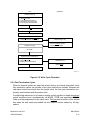
TABLE OF CONTENTS
SECTION 1INTRODUCTION
SECTION 2NOMENCLATURE
2.1
2.2
2.3
2.4
2.5
Symbols and Operators ............................................................................. 2-1
CPU16 Register Mnemonics ..................................................................... 2-2
Pin and Signal Mnemonics ........................................................................ 2-3
Register Mnemonics .................................................................................. 2-5
Conventions .............................................................................................. 2-9
SECTION 3OVERVIEW
3.1
3.1.1
3.1.2
3.1.3
3.1.4
3.1.5
3.1.6
3.1.7
3.1.8
3.1.9
3.1.10
3.1.11
3.2
3.3
3.4
3.5
3.6
3.7
3.8
MC68HC16Y3/916Y3 MCU Features ....................................................... 3-1
Central Processing Unit (CPU16) ...................................................... 3-1
Single-Chip Integration Module 2 (SCIM2) ........................................ 3-1
Standby RAM (SRAM) ...................................................................... 3-1
Masked ROM Module (MRM) — MC68HC16Y3 Only ...................... 3-2
Flash EEPROM Module (FLASH) — MC68HC916Y3 Only .............. 3-2
TPU Flash EEPROM Module (TPUFLASH) — MC68HC916Y3 Only 3-2
Analog-to-Digital Converter (ADC) .................................................... 3-2
Queued Serial Module (QSM) ........................................................... 3-2
Multichannel Communication Interface (MCCI) ................................. 3-2
General Purpose Timer (GPT) .......................................................... 3-2
Time Processor Unit 2 (TPU2) .......................................................... 3-2
Intermodule Bus ........................................................................................ 3-3
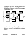
System Block Diagram and Pin Assignment Diagrams ............................. 3-3
Pin Descriptions ........................................................................................ 3-8
Signal Descriptions .................................................................................. 3-12
CPU16 Memory Mapping ........................................................................ 3-17
Internal Register Maps ............................................................................ 3-18
Address Space Maps .............................................................................. 3-21
SECTION 4 CENTRAL PROCESSOR UNIT
4.1
4.2
4.2.1
4.2.2
4.2.3
4.2.4
4.2.5
4.2.6
General ...................................................................................................... 4-1
Register Model .......................................................................................... 4-1
Accumulators ..................................................................................... 4-3
Index Registers ................................................................................. 4-3
Stack Pointer ..................................................................................... 4-3
Program Counter ............................................................................... 4-3
Condition Code Register ................................................................... 4-4
Address Extension Register and Address Extension Fields ............. 4-5
MC68HC16Y3/916Y3
USER’S MANUAL
MOTOROLA
iii
TABLE OF CONTENTS
(Continued)
4.2.7
Multiply and Accumulate Registers ................................................... 4-5
4.3
Memory Management ............................................................................... 4-5
4.3.1
Address Extension ............................................................................ 4-6
4.3.2
Extension Fields ................................................................................ 4-6
4.4
Data Types ................................................................................................ 4-6
4.5
Memory Organization ................................................................................ 4-7
4.6
Addressing Modes ..................................................................................... 4-8
4.6.1
Immediate Addressing Modes ........................................................... 4-9
4.6.2
Extended Addressing Modes .......................................................... 4-10
4.6.3
Indexed Addressing Modes ............................................................. 4-10
4.6.4
Inherent Addressing Mode .............................................................. 4-10
4.6.5
Accumulator Offset Addressing Mode ............................................. 4-10
4.6.6
Relative Addressing Modes ............................................................. 4-10
4.6.7
Post-Modified Index Addressing Mode ............................................ 4-10
4.6.8
Use of CPU16 Indexed Mode to Replace M68HC11 Direct Mode .. 4-11
4.7
Instruction Set ......................................................................................... 4-11
4.7.1
Instruction Set Summary ................................................................. 4-11
4.8
Comparison of CPU16 and M68HC11 CPU Instruction Sets .................. 4-31
4.9
Instruction Format ................................................................................... 4-33
4.10
Execution Model ...................................................................................... 4-34
4.10.1
Microsequencer ............................................................................... 4-35
4.10.2
Instruction Pipeline .......................................................................... 4-35
4.10.3
Execution Unit ................................................................................. 4-35
4.11
Execution Process ................................................................................... 4-36
4.11.1
Changes in Program Flow ............................................................... 4-36
4.12
Instruction Timing .................................................................................... 4-36
4.13
Exceptions ............................................................................................... 4-37
4.13.1
Exception Vectors ........................................................................... 4-37
4.13.2
Exception Stack Frame ................................................................... 4-38
4.13.3
Exception Processing Sequence ..................................................... 4-39
4.13.4
Types of Exceptions ........................................................................ 4-39
4.13.4.1
Asynchronous Exceptions ....................................................... 4-39
4.13.4.2
Synchronous Exceptions ......................................................... 4-39
4.13.5
Multiple Exceptions ......................................................................... 4-40
4.13.6
RTI Instruction ................................................................................. 4-40
4.14
Development Support .............................................................................. 4-40
4.14.1
Deterministic Opcode Tracking ....................................................... 4-40
4.14.1.1
IPIPE0/IPIPE1 Multiplexing ..................................................... 4-41
4.14.1.2
Combining Opcode Tracking with Other Capabilities .............. 4-41
4.14.2
Breakpoints ..................................................................................... 4-41
4.14.3
Opcode Tracking and Breakpoints .................................................. 4-42
MOTOROLA
iv
MC68HC16Y3/916Y3
USER’S MANUAL
TABLE OF CONTENTS
(Continued)
4.14.4
Background Debug Mode ................................................................ 4-42
4.14.5
Enabling BDM ................................................................................. 4-42
4.14.5.1
BDM Sources .......................................................................... 4-42
4.14.5.2
Entering BDM .......................................................................... 4-43
4.14.5.3
BDM Commands ..................................................................... 4-43
4.14.5.4
Returning from BDM ............................................................... 4-44
4.14.5.5
BDM Serial Interface ............................................................... 4-44
4.15
Recommended BDM Connection ............................................................ 4-45
4.16
Digital Signal Processing ......................................................................... 4-46
SECTION 5 SINGLE-CHIP INTEGRATION MODULE 2
5.1
5.2
5.2.1
5.2.2
5.2.3
5.2.4
5.2.5
5.2.6
5.3
5.3.1
5.3.2
5.3.3
5.3.4
5.4
5.4.1
5.4.2
5.4.3
5.4.4
5.4.5
5.4.6
5.4.7
5.4.8
5.5
5.5.1
5.5.1.1
5.5.1.2
5.5.1.3
5.5.1.4
5.5.1.5
5.5.1.6
General ...................................................................................................... 5-1
System Configuration ................................................................................ 5-2
Module Mapping ................................................................................ 5-3
Interrupt Arbitration ............................................................................ 5-3
Single-Chip Operation Support ......................................................... 5-3
Show Internal Cycles ......................................................................... 5-4
Register Access ................................................................................ 5-4
Freeze Operation .............................................................................. 5-4
System Clock ............................................................................................ 5-4
Clock Sources ................................................................................... 5-5
Clock Synthesizer Operation ............................................................. 5-6
External Bus Clock .......................................................................... 5-14
Low-Power Operation ...................................................................... 5-14
System Protection ................................................................................... 5-16
Reset Status .................................................................................... 5-16
Bus Monitor ..................................................................................... 5-16
Halt Monitor ..................................................................................... 5-17
Spurious Interrupt Monitor ............................................................... 5-17
Software Watchdog ......................................................................... 5-17
Periodic Interrupt Timer ................................................................... 5-19
Interrupt Priority and Vectoring ........................................................ 5-20
Low-Power STOP Operation ........................................................... 5-21
External Bus Interface ............................................................................. 5-21
Bus Control Signals ......................................................................... 5-23
Address Bus ............................................................................ 5-23
Address Strobe ....................................................................... 5-23
Data Bus ................................................................................. 5-23
Data Strobe ............................................................................. 5-23
Read/Write Signal ................................................................... 5-24
Size Signals ............................................................................ 5-24
MC68HC16Y3/916Y3
USER’S MANUAL
MOTOROLA
v
TABLE OF CONTENTS
(Continued)
5.5.1.7
Function Codes ....................................................................... 5-24
5.5.1.8
Data Size Acknowledge Signals ............................................. 5-24
5.5.1.9
Bus Error Signal ...................................................................... 5-25
5.5.1.10
Halt Signal ............................................................................... 5-25
5.5.1.11
Autovector Signal .................................................................... 5-25
5.5.2
Dynamic Bus Sizing ........................................................................ 5-25
5.5.3
Operand Alignment ......................................................................... 5-27
5.5.4
Misaligned Operands ...................................................................... 5-27
5.5.5
Operand Transfer Cases ................................................................. 5-27
5.6
Bus Operation ......................................................................................... 5-28
5.6.1
Synchronization to CLKOUT ........................................................... 5-29
5.6.2
Regular Bus Cycle ........................................................................... 5-29
5.6.2.1
Read Cycle .............................................................................. 5-30
5.6.2.2
Write Cycle .............................................................................. 5-30
5.6.3
Fast Termination Cycles .................................................................. 5-31
5.6.4
CPU Space Cycles .......................................................................... 5-32
5.6.4.1
Breakpoint Acknowledge Cycle ............................................... 5-33
5.6.4.2
LPSTOP Broadcast Cycle ....................................................... 5-34
5.6.5
Bus Exception Control Cycles ......................................................... 5-35
5.6.5.1
Bus Errors ............................................................................... 5-36
5.6.5.2
Double Bus Faults ................................................................... 5-37
5.6.5.3
Halt Operation ......................................................................... 5-37
5.6.6
External Bus Arbitration ................................................................... 5-38
5.6.6.1
Show Cycles ........................................................................... 5-39
5.7
Reset ....................................................................................................... 5-40
5.7.1
Reset Exception Processing ........................................................... 5-40
5.7.2
Reset Control Logic ......................................................................... 5-40
5.7.3
Operating Configuration Out of Reset ............................................. 5-41
5.7.3.1
Address and Data Bus Pin Functions ..................................... 5-42
5.7.3.2
Data Bus Mode Selection ........................................................ 5-43
5.7.3.3
16-Bit Expanded Mode ............................................................ 5-45
5.7.3.4
8-Bit Expanded Mode .............................................................. 5-47
5.7.3.5
Single-Chip Mode .................................................................... 5-48
5.7.3.6
Clock Mode Selection ............................................................. 5-48
5.7.3.7
Breakpoint Mode Selection ..................................................... 5-49
5.7.3.8
Emulation Mode Selection ...................................................... 5-49
5.7.4
MCU Module Pin Function During Reset ........................................ 5-50
5.7.5
Pin State During Reset .................................................................... 5-51
5.7.5.1
Reset States of SCIM2 Pins .................................................... 5-51
5.7.5.2
Reset States of Pins Assigned to Other MCU Modules .......... 5-52
5.7.6
Reset Timing ................................................................................... 5-52
MOTOROLA
vi
MC68HC16Y3/916Y3
USER’S MANUAL
TABLE OF CONTENTS
(Continued)
5.7.7
5.7.8
5.7.9
5.7.10
5.8
5.8.1
5.8.2
5.8.3
5.8.4
5.8.5
5.9
5.9.1
5.9.1.1
5.9.1.2
5.9.1.3
5.9.1.4
5.9.2
5.9.3
5.9.4
5.10
5.10.1
5.10.2
5.10.3
5.10.4
5.10.5
5.11
Power-On Reset .............................................................................. 5-53
Use of the Three-State Control Pin ................................................. 5-54
Reset Processing Summary ............................................................ 5-54
Reset Status Register ..................................................................... 5-55
Interrupts ................................................................................................. 5-55
Interrupt Exception Processing ....................................................... 5-56
Interrupt Priority and Recognition .................................................... 5-56
Interrupt Acknowledge and Arbitration ............................................ 5-57
Interrupt Processing Summary ........................................................ 5-58
Interrupt Acknowledge Bus Cycles .................................................. 5-59
Chip-Selects ............................................................................................ 5-60
Chip-Select Registers ...................................................................... 5-63
Chip-Select Pin Assignment Registers ................................... 5-63
Chip-Select Base Address Registers ...................................... 5-64
Chip-Select Option Registers .................................................. 5-65
PORTC Data Register ............................................................. 5-66
Chip-Select Operation ..................................................................... 5-67
Using Chip-Select Signals for Interrupt Acknowledge ..................... 5-67
Chip-Select Reset Operation ........................................................... 5-69
General Purpose Input/Output ................................................................ 5-70
Ports A and B .................................................................................. 5-71
Port E .............................................................................................. 5-71
Port F ............................................................................................... 5-72
Port G .............................................................................................. 5-74
Port H .............................................................................................. 5-74
Factory Test ............................................................................................ 5-75
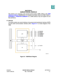
SECTION 6STANDBY RAM MODULE
6.1
6.2
6.3
6.4
6.5
6.6
SRAM Register Block ................................................................................ 6-1
SRAM Array Address Mapping ................................................................. 6-1
SRAM Array Address Space Type ............................................................ 6-2
Normal Access .......................................................................................... 6-2
Standby and Low-Power Stop Operation .................................................. 6-2
Reset ......................................................................................................... 6-2
SECTION 7MASKED ROM MODULE
7.1
7.2
7.3
7.4
MRM Register Block .................................................................................. 7-1
MRM Array Address Mapping ................................................................... 7-1
MRM Array Address Space Type .............................................................. 7-2
Normal Access .......................................................................................... 7-2
MC68HC16Y3/916Y3
USER’S MANUAL
MOTOROLA
vii
TABLE OF CONTENTS
(Continued)
7.5
7.6
7.7
Low-Power Stop Mode Operation ............................................................. 7-3
ROM Signature .......................................................................................... 7-3
Reset ......................................................................................................... 7-3
SECTION 8FLASH EEPROM MODULE
8.1
Flash EEPROM Control Block ................................................................... 8-1
8.2
Flash EEPROM Array ............................................................................... 8-2
8.3
Flash EEPROM Operation ........................................................................ 8-2
8.3.1
Reset Operation ................................................................................ 8-2
8.3.2
Bootstrap Operation .......................................................................... 8-3
8.3.3
Normal Operation .............................................................................. 8-3
8.3.4
Program/Erase Operation ................................................................. 8-3
8.3.5
Programming ..................................................................................... 8-4
8.3.5.1
Erasure ...................................................................................... 8-6
SECTION 9TPU FLASH EEPROM MODULE
9.1
9.2
9.3
9.4
9.4.1
9.4.2
9.4.3
9.4.4
9.4.5
9.4.5.1
9.4.5.2
Overview ................................................................................................... 9-1
TPUFLASH Control Block ......................................................................... 9-1
TPUFLASH Array ...................................................................................... 9-2
TPUFLASH Operation ............................................................................... 9-2
Reset Operation ................................................................................ 9-2
Bootstrap Operation .......................................................................... 9-3
Normal Operation .............................................................................. 9-3
TPU Mode Operation ........................................................................ 9-3
Program/Erase Operation ................................................................. 9-4
Programming Sequence ........................................................... 9-5
Erasure Sequence .................................................................... 9-7
SECTION 10ANALOG-TO-DIGITAL CONVERTER
10.1
10.2
10.2.1
10.2.2
10.2.3
10.3
10.4
10.5
10.5.1
10.5.2
General .................................................................................................... 10-1
External Connections .............................................................................. 10-1
Analog Input Pins ............................................................................ 10-2
Analog Reference Pins .................................................................... 10-3
Analog Supply Pins ......................................................................... 10-3
Programmer’s Model ............................................................................... 10-3
ADC Bus Interface Unit ........................................................................... 10-3
Special Operating Modes ........................................................................ 10-3
Low-Power Stop Mode .................................................................... 10-4
Freeze Mode ................................................................................... 10-4
MOTOROLA
viii
MC68HC16Y3/916Y3
USER’S MANUAL
TABLE OF CONTENTS
(Continued)
10.6
Analog Subsystem .................................................................................. 10-4
10.6.1
Multiplexer ....................................................................................... 10-5
10.6.2
Sample Capacitor and Buffer Amplifier ........................................... 10-5
10.6.3
RC DAC Array ................................................................................. 10-6
10.6.4
Comparator ..................................................................................... 10-6
10.7
Digital Control Subsystem ....................................................................... 10-6
10.7.1
Control/Status Registers ................................................................. 10-6
10.7.2
Clock and Prescaler Control ............................................................ 10-6
10.7.3
Sample Time ................................................................................... 10-7
10.7.4
Resolution ....................................................................................... 10-7
10.7.5
Conversion Control Logic ................................................................ 10-7
10.7.5.1
Conversion Parameters .......................................................... 10-8
10.7.5.2
Conversion Modes .................................................................. 10-8
10.7.6
Conversion Timing ........................................................................ 10-12
10.7.7
Successive Approximation Register .............................................. 10-13
10.7.8
Result Registers ............................................................................ 10-13
10.8
Pin Considerations ................................................................................ 10-14
10.8.1
Analog Reference Pins .................................................................. 10-14
10.8.2
Analog Power Pins ........................................................................ 10-14
10.8.3
Analog Supply Filtering and Grounding ......................................... 10-16
10.8.4
Accommodating Positive/Negative Stress Conditions ................... 10-18
10.8.5
Analog Input Considerations ......................................................... 10-20
10.8.6
Analog Input Pins .......................................................................... 10-22
10.8.6.1
Settling Time for the External Circuit ..................................... 10-23
10.8.6.2
Error Resulting from Leakage ............................................... 10-24
SECTION 11
QUEUED SERIAL MODULE
11.1
General .................................................................................................... 11-1
11.2
QSM Registers and Address Map ........................................................... 11-2
11.2.1
QSM Global Registers ..................................................................... 11-2
11.2.1.1
Low-Power Stop Mode Operation ........................................... 11-2
11.2.1.2
Freeze Operation .................................................................... 11-3
11.2.1.3
QSM Interrupts ........................................................................ 11-3
11.2.2
QSM Pin Control Registers ............................................................. 11-4
11.3
Queued Serial Peripheral Interface ......................................................... 11-5
11.3.1
QSPI Registers ................................................................................ 11-7
11.3.1.1
Control Registers .................................................................... 11-7
11.3.1.2
Status Register ........................................................................ 11-7
11.3.2
QSPI RAM ....................................................................................... 11-8
11.3.2.1
Receive RAM .......................................................................... 11-8
MC68HC16Y3/916Y3
USER’S MANUAL
MOTOROLA
ix
TABLE OF CONTENTS
(Continued)
11.3.2.2
Transmit RAM ......................................................................... 11-8
11.3.2.3
Command RAM ....................................................................... 11-9
11.3.3
QSPI Pins ........................................................................................ 11-9
11.3.4
QSPI Operation ............................................................................... 11-9
11.3.5
QSPI Operating Modes ................................................................. 11-10
11.3.5.1
Master Mode ......................................................................... 11-17
11.3.5.2
Master Wrap-Around Mode ................................................... 11-20
11.3.5.3
Slave Mode ........................................................................... 11-21
11.3.5.4
Slave Wrap-Around Mode ..................................................... 11-22
11.3.6
Peripheral Chip-Selects ................................................................. 11-22
11.4
Serial Communication Interface ............................................................ 11-22
11.4.1
SCI Registers ................................................................................ 11-23
11.4.1.1
Control Registers .................................................................. 11-23
11.4.1.2
Status Register ...................................................................... 11-26
11.4.1.3
Data Register ........................................................................ 11-26
11.4.2
SCI Pins ........................................................................................ 11-26
11.4.3
SCI Operation ................................................................................ 11-26
11.4.3.1
Definition of Terms ................................................................ 11-26
11.4.3.2
Serial Formats ....................................................................... 11-27
11.4.3.3
Baud Clock ............................................................................ 11-27
11.4.3.4
Parity Checking ..................................................................... 11-28
11.4.3.5
Transmitter Operation ........................................................... 11-28
11.4.3.6
Receiver Operation ............................................................... 11-30
11.4.3.7
Idle-Line Detection ................................................................ 11-31
11.4.3.8
Receiver Wake-up ................................................................. 11-31
11.4.3.9
Internal Loop Mode ............................................................... 11-32
SECTION 12 MULTICHANNEL COMMUNICATION INTERFACE
12.1
General .................................................................................................... 12-1
12.2
MCCI Registers and Address Map .......................................................... 12-2
12.2.1
MCCI Global Registers .................................................................... 12-2
12.2.1.1
Low-Power Stop Mode ............................................................ 12-2
12.2.1.2
Privilege Levels ....................................................................... 12-3
12.2.1.3
MCCI Interrupts ....................................................................... 12-3
12.2.2
Pin Control and General-Purpose I/O ............................................. 12-4
12.3
Serial Peripheral Interface (SPI) .............................................................. 12-4
12.3.1
SPI Registers .................................................................................. 12-6
12.3.1.1
SPI Control Register (SPCR) .................................................. 12-6
12.3.1.2
SPI Status Register (SPSR) .................................................... 12-6
12.3.1.3
SPI Data Register (SPDR) ...................................................... 12-6
12.3.2
SPI Pins ........................................................................................... 12-7
MOTOROLA
x
MC68HC16Y3/916Y3
USER’S MANUAL
TABLE OF CONTENTS
(Continued)
12.3.3
SPI Operating Modes ...................................................................... 12-7
12.3.3.1
Master Mode ........................................................................... 12-7
12.3.3.2
Slave Mode ............................................................................. 12-8
12.3.4
SPI Clock Phase and Polarity Controls ........................................... 12-9
12.3.4.1
CPHA = 0 Transfer Format ..................................................... 12-9
12.3.4.2
CPHA = 1 Transfer Format ................................................... 12-10
12.3.5
SPI Serial Clock Baud Rate .......................................................... 12-11
12.3.6
Wired-OR Open-Drain Outputs ..................................................... 12-12
12.3.7
Transfer Size and Direction ........................................................... 12-12
12.3.8
Write Collision ............................................................................... 12-12
12.3.9
Mode Fault .................................................................................... 12-12
12.4
Serial Communication Interface (SCI) ................................................... 12-13
12.4.1
SCI Registers ................................................................................ 12-13
12.4.1.1
SCI Control Registers ........................................................... 12-14
12.4.1.2
SCI Status Register ............................................................... 12-17
12.4.1.3
SCI Data Register ................................................................. 12-17
12.4.2
SCI Pins ........................................................................................ 12-17
12.4.3
Receive Data Pins (RXDA, RXDB) ............................................... 12-18
12.4.4
Transmit Data Pins (TXDA, TXDB) ............................................... 12-18
12.4.5
SCI Operation ................................................................................ 12-18
12.4.5.1
Definition of Terms ................................................................ 12-18
12.4.5.2
Serial Formats ....................................................................... 12-19
12.4.5.3
Baud Clock ............................................................................ 12-19
12.4.5.4
Parity Checking ..................................................................... 12-20
12.4.5.5
Transmitter Operation ........................................................... 12-20
12.4.5.6
Receiver Operation ............................................................... 12-21
12.4.5.7
Idle-Line Detection ................................................................ 12-22
12.4.5.8
Receiver Wake-Up ................................................................ 12-23
12.4.5.9
Internal Loop ......................................................................... 12-23
12.5
MCCI Initialization ................................................................................. 12-24
SECTION 13 GENERAL-PURPOSE TIMER
13.1
13.2
13.3
13.3.1
13.3.2
13.3.3
13.3.4
13.4
13.4.1
General .................................................................................................... 13-1
GPT Registers and Address Map ............................................................ 13-2
Special Modes of Operation .................................................................... 13-3
Low-Power Stop Mode .................................................................... 13-3
Freeze Mode ................................................................................... 13-3
Single-Step Mode ............................................................................ 13-4
Test Mode ....................................................................................... 13-4
Polled and Interrupt-Driven Operation ..................................................... 13-4
Polled Operation .............................................................................. 13-4
MC68HC16Y3/916Y3
USER’S MANUAL
MOTOROLA
xi
TABLE OF CONTENTS
(Continued)
13.4.2
13.5
13.5.1
13.5.2
13.5.3
13.5.4
13.5.5
13.5.6
13.6
13.7
13.8
13.8.1
13.8.2
13.8.3
13.9
13.10
13.11
13.11.1
13.11.2
GPT Interrupts ................................................................................. 13-5
Pin Descriptions ...................................................................................... 13-7
Input Capture Pins ........................................................................... 13-7
Input Capture/Output Compare Pin ................................................. 13-7
Output Compare Pins ...................................................................... 13-7
Pulse Accumulator Input Pin ........................................................... 13-8
Pulse-Width Modulation .................................................................. 13-8
Auxiliary Timer Clock Input .............................................................. 13-8
General-Purpose I/O ............................................................................... 13-8
Prescaler ................................................................................................. 13-9
Capture/Compare Unit .......................................................................... 13-11
Timer Counter ............................................................................... 13-11
Input Capture Functions ................................................................ 13-11
Output Compare Functions ........................................................... 13-14
Input Capture 4/Output Compare 5 ....................................................... 13-15
Pulse Accumulator ................................................................................ 13-15
Pulse-Width Modulation Unit ................................................................. 13-17
PWM Counter ................................................................................ 13-19
PWM Function ............................................................................... 13-19
SECTION 14 TIME PROCESSOR UNIT 2
14.1
14.2
14.2.1
14.2.2
14.2.3
14.2.4
14.2.5
14.2.6
14.3
14.3.1
14.3.2
14.3.3
14.3.4
14.3.5
14.3.6
14.3.7
14.4
14.4.1
14.4.2
14.4.3
General .................................................................................................... 14-1
TPU2 Components .................................................................................. 14-2
Time Bases ..................................................................................... 14-2
Timer Channels ............................................................................... 14-3
Scheduler ........................................................................................ 14-3
Microengine ..................................................................................... 14-3
Host Interface .................................................................................. 14-3
Parameter RAM ............................................................................... 14-3
TPU Operation ........................................................................................ 14-4
Event Timing ................................................................................... 14-4
Channel Orthogonality ..................................................................... 14-4
Interchannel Communication ........................................................... 14-4
Programmable Channel Service Priority ......................................... 14-5
Coherency ....................................................................................... 14-5
Emulation Support ........................................................................... 14-5
TPU2 Interrupts ............................................................................... 14-5
A Mask Set Time Functions .................................................................... 14-6
Discrete Input/Output (DIO) ............................................................. 14-6
Input Capture/Input Transition Counter (ITC) .................................. 14-7
Output Compare (OC) ..................................................................... 14-7
MOTOROLA
xii
MC68HC16Y3/916Y3
USER’S MANUAL
TABLE OF CONTENTS
(Continued)
14.4.4
Pulse-Width Modulation (PWM) ...................................................... 14-8
14.4.5
Synchronized Pulse-Width Modulation (SPWM) ............................. 14-8
14.4.6
Period Measurement with Additional Transition Detect (PMA) ....... 14-8
14.4.7
Period Measurement with Missing Transition Detect (PMM) .......... 14-8
14.4.8
Position-Synchronized Pulse Generator (PSP) ............................... 14-9
14.4.9
Stepper Motor (SM) ......................................................................... 14-9
14.4.10
Period/Pulse-Width Accumulator (PPWA) ..................................... 14-10
14.4.11
Quadrature Decode (QDEC) ......................................................... 14-10
14.5
G Mask Set Time Functions .................................................................. 14-11
14.5.1
Table Stepper Motor (TSM) ........................................................... 14-11
14.5.2
New Input Capture/Transition Counter (NITC) .............................. 14-11
14.5.3
Queued Output Match (QOM) ....................................................... 14-11
14.5.4
Programmable Time Accumulator (PTA) ...................................... 14-12
14.5.5
Multichannel Pulse-Width Modulation (MCPWM) ......................... 14-12
14.5.6
Fast Quadrature Decode (FQD) .................................................... 14-12
14.5.7
Universal Asynchronous Receiver/Transmitter (UART) ................ 14-13
14.5.8
Brushless Motor Commutation (COMM) ....................................... 14-13
14.5.9
Frequency Measurement (FQM) ................................................... 14-13
14.5.10
Hall Effect Decode (HALLD) .......................................................... 14-13
14.6
Host Interface Registers ........................................................................ 14-14
14.6.1
System Configuration Registers .................................................... 14-14
14.6.1.1
Prescaler Control for TCR1 ................................................... 14-14
14.6.1.2
Prescaler Control for TCR2 ................................................... 14-15
14.6.1.3
Emulation Control .................................................................. 14-16
14.6.1.4
Low-Power Stop Control ....................................................... 14-16
14.6.2
Channel Control Registers ............................................................ 14-16
14.6.2.1
Channel Interrupt Enable and Status Registers .................... 14-17
14.6.2.2
Channel Function Select Registers ....................................... 14-17
14.6.2.3
Host Sequence Registers ..................................................... 14-18
14.6.2.4
Host Service Registers .......................................................... 14-18
14.6.2.5
Channel Priority Registers .................................................... 14-18
14.6.3
Development Support and Test Registers .................................... 14-18
APPENDIX A ELECTRICAL CHARACTERISTICS
APPENDIX B MECHANICAL DATA AND ORDERING INFORMATION
B.1
B.2
Obtaining Updated MC68HC16Y3/916Y3 MCU Mechanical Information B-5
Ordering Information ................................................................................ B-5
APPENDIX C DEVELOPMENT SUPPORT
MC68HC16Y3/916Y3
USER’S MANUAL
MOTOROLA
xiii
TABLE OF CONTENTS
(Continued)
C.1
C.2
M68MMDS1632 Modular Development System ...................................... C-1
M68MEVB1632 Modular Evaluation Board .............................................. C-1
APPENDIX D REGISTER SUMMARY
D.1
Central Processing Unit ............................................................................ D-1
D.1.1
Condition Code Register .................................................................. D-3
D.2
Single-Chip Integration Module 2 ............................................................. D-4
D.2.1
SCIM Configuration Register ............................................................ D-5
D.2.2
SCIM Test Register .......................................................................... D-7
D.2.3
Clock Synthesizer Control Register .................................................. D-7
D.2.4
Reset Status Register ...................................................................... D-9
D.2.5
SCIM Test Register E ....................................................................... D-9
D.2.6
Port A and B Data Registers ............................................................ D-9
D.2.7
Port G and H Data Registers .......................................................... D-10
D.2.8
Port G and H Data Direction Registers .......................................... D-10
D.2.9
Port E Data Register ...................................................................... D-10
D.2.10
Port E Data Direction Register ....................................................... D-11
D.2.11
Port E Pin Assignment Register ..................................................... D-11
D.2.12
Port F Data Register ....................................................................... D-12
D.2.13
Port F Data Direction Register ....................................................... D-12
D.2.14
Port F Pin Assignment Register ..................................................... D-12
D.2.15
System Protection Control Register ............................................... D-13
D.2.16
Periodic Interrupt Control Register ................................................. D-15
D.2.17
Periodic Interrupt Timer Register ................................................... D-15
D.2.18
Software Watchdog Service Register ............................................. D-16
D.2.19
Port F Edge-Detect Flag Register .................................................. D-16
D.2.20
Port F Edge-Detect Interrupt Vector ............................................... D-17
D.2.21
Port F Edge-Detect Interrupt Level ................................................. D-17
D.2.22
Port C Data Register ...................................................................... D-17
D.2.23
Chip-Select Pin Assignment Registers ........................................... D-18
D.2.24
Chip-Select Base Address Register Boot ....................................... D-20
D.2.25
Chip-Select Base Address Registers ............................................. D-20
D.2.26
Chip-Select Option Register Boot .................................................. D-21
D.2.27
Chip-Select Option Registers ......................................................... D-21
D.2.28
Master Shift Registers .................................................................... D-23
D.2.29
Test Module Shift Count Register .................................................. D-24
D.2.30
Test Module Repetition Count Register ......................................... D-24
D.2.31
Test Module Control Register ......................................................... D-24
D.2.32
Test Module Distributed Register ................................................... D-24
D.3
Standby RAM Module ............................................................................ D-25
D.3.1
RAM Module Configuration Register .............................................. D-25
MOTOROLA
xiv
MC68HC16Y3/916Y3
USER’S MANUAL
TABLE OF CONTENTS
(Continued)
D.3.2
D.3.3
D.4
D.4.1
D.4.2
D.4.3
D.4.4
D.5
D.5.1
D.5.2
D.5.3
D.5.4
D.6
D.6.1
D.6.2
D.6.3
D.6.4
D.6.5
D.6.6
D.6.7
D.7
D.7.1
D.7.2
D.7.3
D.7.4
D.7.5
D.7.6
D.7.7
D.7.8
D.7.9
D.7.10
D.7.11
D.7.12
D.7.13
D.7.14
D.7.15
D.7.16
D.8
D.8.1
D.8.2
D.8.3
RAM Test Register ......................................................................... D-26
Array Base Address Registers ....................................................... D-26
Masked ROM Module ............................................................................. D-27
Masked ROM Module Configuration Register ................................ D-27
ROM Array Base Address Registers .............................................. D-29
ROM Signature Registers .............................................................. D-29
ROM Bootstrap Words ................................................................... D-30
Flash EEPROM Module ......................................................................... D-31
Flash EEPROM Module Configuration Register ............................ D-32
Flash EEPROM Test Register ........................................................ D-34
Flash EEPROM Base Address Registers ...................................... D-34
Flash EEPROM Control Register ................................................... D-35
Analog-to-Digital Converter Module ....................................................... D-37
ADC Module Configuration Register .............................................. D-38
ADC Test Register ......................................................................... D-38
Port ADA Data Register ................................................................. D-38
ADC Control Register 0 .................................................................. D-39
ADC Control Register 1 .................................................................. D-40
ADC Status Register ...................................................................... D-44
Right Justified, Unsigned Result Register ...................................... D-44
Queued Serial Module ............................................................................ D-46
QSM Configuration Register .......................................................... D-46
QSM Test Register ......................................................................... D-47
QSM Interrupt Level Register/Interrupt Vector Register ................. D-47
SCI Control Register ...................................................................... D-48
SCI Control Register 1 ................................................................... D-49
SCI Status Register ........................................................................ D-51
SCI Data Register .......................................................................... D-52
Port QS Data Register .................................................................... D-52
Port QS Pin Assignment Register/Data Direction Register ............ D-53
QSPI Control Register 0 ................................................................. D-54
QSPI Control Register 1 ................................................................. D-56
QSPI Control Register 2 ................................................................. D-57
QSPI Control Register 3 ................................................................. D-58
Receive Data RAM ......................................................................... D-59
Transmit Data RAM ........................................................................ D-59
Command RAM .............................................................................. D-60
Multichannel Communication Interface Module (MCCI) ......................... D-62
MCCI Module Configuration Register ............................................. D-62
MCCI Test Register ........................................................................ D-63
SCI Interrupt Level Register/MCCI Interrupt Vector Register ......... D-63
MC68HC16Y3/916Y3
USER’S MANUAL
MOTOROLA
xv
TABLE OF CONTENTS
(Continued)
D.8.4
MCCI Interrupt Vector Register ...................................................... D-64
D.8.5
SPI Interrupt Level Register ........................................................... D-64
D.8.6
MCCI Pin Assignment Register ...................................................... D-65
D.8.7
MCCI Data Direction Register ........................................................ D-66
D.8.8
MCCI Port Data Registers .............................................................. D-67
D.8.9
SCI Control Register 0 ................................................................... D-67
D.8.11
SCI Status Register ........................................................................ D-70
D.8.12
SCI Data Register .......................................................................... D-71
D.8.13
SPI Control Register ....................................................................... D-72
D.8.14
SPI Status Register ........................................................................ D-73
D.8.15
SPI Data Register ........................................................................... D-74
D.9
General-Purpose Timer (GPT) ............................................................... D-75
D.9.1
GPT Module Configuration Register .............................................. D-75
D.9.2
GPT Test Register .......................................................................... D-76
D.9.3
GPT Interrupt Configuration Register ............................................. D-76
D.9.4
Port GP Data Direction Register/Data Register ............................. D-77
D.9.5
OC1 Action Mask Register/Data Register ...................................... D-77
D.9.6
Timer Counter Register .................................................................. D-78
D.9.7
Pulse Accumulator Control Register/Counter ................................. D-78
D.9.8
Input Capture Registers 1-3 ........................................................... D-79
D.9.9
Output Compare Registers 1-4 ...................................................... D-79
D.9.10
Input Capture 4/Output Compare 5 Register .................................. D-80
D.9.11
Timer Control Registers 1 and 2 .................................................... D-80
D.9.12
Timer Interrupt Mask Registers 1 and 2 ......................................... D-80
D.9.13
Timer Interrupt Flag Registers 1 and 2 ........................................... D-82
D.9.14
Compare Force Register/PWM Control Register C ........................ D-82
D.9.15
PWM Registers A/B ........................................................................ D-84
D.9.16
PWM Count Register ...................................................................... D-84
D.9.17
PWM Buffer Registers A/B ............................................................. D-84
D.9.18
GPT Prescaler ................................................................................ D-85
D.10
Time Processor Unit 2 (TPU2) ............................................................... D-86
D.10.1
TPU2 Module Configuration Register ............................................. D-87
D.10.2
TPU2 Test Configuration Register ................................................. D-89
D.10.3
Development Support Control Register .......................................... D-89
D.10.4
Development Support Status Register ........................................... D-90
D.10.5
TPU2 Interrupt Configuration Register ........................................... D-91
D.10.6
Channel Interrupt Enable Register ................................................. D-91
D.10.7
Channel Function Select Registers ................................................ D-92
D.10.8
Host Sequence Registers ............................................................... D-92
D.10.9
Host Service Request Registers .................................................... D-93
D.10.10
Channel Priority Registers .............................................................. D-93
MOTOROLA
xvi
MC68HC16Y3/916Y3
USER’S MANUAL
TABLE OF CONTENTS
(Continued)
D.10.11
Channel Interrupt Status Register .................................................. D-94
D.10.12
Link Register .................................................................................. D-94
D.10.13
Service Grant Latch Register ......................................................... D-94
D.10.14
Decoded Channel Number Register .............................................. D-94
D.10.15
TPUMCR2 Module Configuration Register 2 ................................. D-94
D.10.16
TPU2 Parameter RAM ................................................................... D-96
D.11
TPU Flash EEPROM Module (TPUFLASH) ........................................... D-98
D.11.1
TPUFLASH Module Configuration Register ................................... D-98
D.11.2
TPUFLASH Test Register ............................................................ D-101
D.11.3
TPUFLASH Base Address Registers ........................................... D-101
D.11.4
TPUFLASH Control Register ........................................................ D-101
D.11.5
TPUFLASH Bootstrap Words ....................................................... D-103
MC68HC16Y3/916Y3
USER’S MANUAL
MOTOROLA
xvii
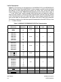
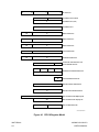
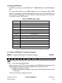
LIST OF ILLUSTRATIONS
Figure
3-1
3-2
3-3
3-4
3-5
3-6
3-7
3-8
3-9
3-10
3-11
4-1
4-2
4-3
4-4
4-5
4-7
4-8
5-1
5-2
5-3
5-4
5-5
5-6
5-7
5-8
5-9
5-10
5-11
5-12
5-13
5-14
5-15
5-16
5-17
5-18
5-19
5-20
5-21
5-22
5-23
Title
Page
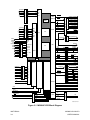
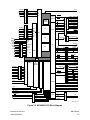
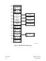
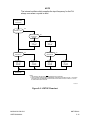
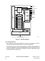
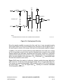
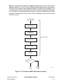
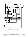
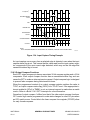
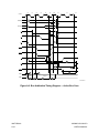
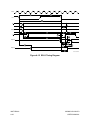
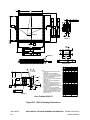
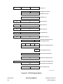
MC68HC16Y3 Block Diagram ........................................................................ 3-4
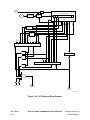
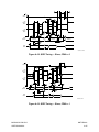
MC68HC916Y3 Block Diagram ...................................................................... 3-5
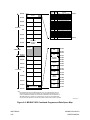
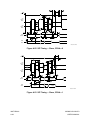
MC68HC16Y3 Pin Assignment for 160-Pin Package ..................................... 3-6
MC68HC916Y3 Pin Assignment for 160-Pin Package ................................... 3-7
Address Bus Connections Between the CPU16 and IMB ............................ 3-17
MC68HC16Y3 Address Map ........................................................................ 3-19
MC68HC916Y3 Address Map ...................................................................... 3-20
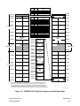
MC68HC16Y3 Combined Program and Data Space Map ........................... 3-22
MC68HC16Y3 Separate Program and Data Space Map ............................. 3-23
MC68HC916Y3 Combined Program and Data Space Map ......................... 3-24
MC68HC916Y3 Separate Program and Data Space Map ........................... 3-25
CPU16 Register Model ................................................................................... 4-2
Condition Code Register ................................................................................ 4-4
Data Types and Memory Organization ........................................................... 4-8
Basic Instruction Formats ............................................................................. 4-34
Instruction Execution Model ......................................................................... 4-35
BDM Serial I/O Block Diagram ..................................................................... 4-45
BDM Connector Pinout ................................................................................. 4-45
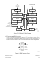
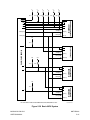
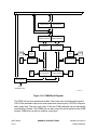
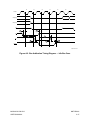
SCIM2 Block Diagram .................................................................................... 5-2
System Clock Block Diagram ......................................................................... 5-5
Slow Reference Crystal Circuit ....................................................................... 5-6
Fast Reference Crystal Circuit ....................................................................... 5-6
System Clock Filter Networks ........................................................................ 5-7
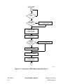
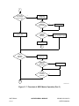
LPSTOP Flowchart ....................................................................................... 5-15
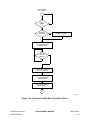
System Protection ........................................................................................ 5-16
Periodic Interrupt Timer and Software Watchdog Timer .............................. 5-19
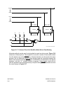
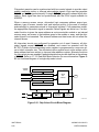
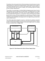
MCU Basic System ...................................................................................... 5-22
Operand Byte Order ..................................................................................... 5-26
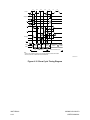
Word Read Cycle Flowchart ......................................................................... 5-30
Write Cycle Flowchart .................................................................................. 5-31
CPU Space Address Encoding .................................................................... 5-33
Breakpoint Operation Flowchart ................................................................... 5-34
LPSTOP Interrupt Mask Level ...................................................................... 5-35
Bus Arbitration Flowchart for Single Request ............................................... 5-39
Preferred Circuit for Data Bus Mode Select Conditioning ............................ 5-44
Alternate Circuit for Data Bus Mode Select Conditioning ............................. 5-45
Power-On Reset ........................................................................................... 5-54
Basic MCU System ...................................................................................... 5-61
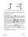
Chip-Select Circuit Block Diagram ............................................................... 5-62
CPU Space Encoding for Interrupt Acknowledge ......................................... 5-68
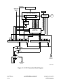
Port F Block Diagram ................................................................................... 5-73
MC68HC16Y3/916Y3
USER’S MANUAL
MOTOROLA
xviii
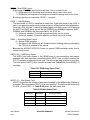
LIST OF ILLUSTRATIONS
(Continued)
Title
Figure
8-1
8-2
9-1
9-2
10-1
10-2
10-3
10-4
10-5
10-6
10-7
10-8
10-9
10-10
11-1
11-2
11-3
11-4
11-5
11-6
11-7
11-8
11-9
11-10
11-11
12-1
12-2
12-3
12-4
12-5
12-6
13-1
13-2
13-3
13-4
13-5
13-6
14-1
14-2
14-3
A-1
Page
Programming Flow ......................................................................................... 8-5
Erasure Flow .................................................................................................. 8-7
TPUFLASH Programming Flow ..................................................................... 9-6
TPUFLASH Erasure Flow .............................................................................. 9-8
ADC Block Diagram ..................................................................................... 10-2
8-Bit Conversion Timing ............................................................................. 10-12
10-Bit Conversion Timing ........................................................................... 10-13
Analog Input Circuitry ................................................................................. 10-15
Errors Resulting from Clipping ................................................................... 10-16
Star-Ground at the Point of Power Supply Origin ....................................... 10-17
Input Pin Subjected to Negative Stress ...................................................... 10-19
Voltage LImiting Diodes in a Negative Stress Circuit ................................. 10-20
External Multiplexing Of Analog Signal Sources ........................................ 10-21
Electrical Model of an A/D Input Pin ........................................................... 10-22
QSM Block Diagram ..................................................................................... 11-1
QSPI Block Diagram .................................................................................... 11-6
QSPI RAM .................................................................................................... 11-8
Flowchart of QSPI Initialization Operation .................................................. 11-11
Flowchart of QSPI Master Operation (Part 1) ............................................ 11-12
Flowchart of QSPI Master Operation (Part 2) ............................................ 11-13
Flowchart of QSPI Master Operation (Part 3) ............................................ 11-14
Flowchart of QSPI Slave Operation (Part 1) .............................................. 11-15
Flowchart of QSPI Slave Operation (Part 2) .............................................. 11-16
SCI Transmitter Block Diagram .................................................................. 11-24
SCI Receiver Block Diagram ...................................................................... 11-25
MCCI Block Diagram .................................................................................... 12-1
SPI Block Diagram ....................................................................................... 12-5
CPHA = 0 SPI Transfer Format .................................................................... 12-9
CPHA = 1 SPI Transfer Format .................................................................. 12-10
SCI Transmitter Block Diagram .................................................................. 12-15
SCI Receiver Block Diagram ...................................................................... 12-16
GPT Block Diagram ...................................................................................... 13-2
Prescaler Block Diagram ............................................................................ 13-10
Capture/Compare Unit Block Diagram ....................................................... 13-12
Input Capture Timing Example ................................................................... 13-14
Pulse Accumulator Block Diagram ............................................................. 13-16
PWM Block Diagram .................................................................................. 13-18
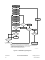
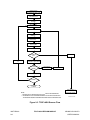
TPU2 Block Diagram .................................................................................... 14-1
TCR1 Prescaler Control ............................................................................. 14-15
TCR2 Prescaler Control ............................................................................. 14-15
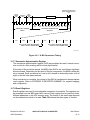
CLKOUT Output Timing Diagram ................................................................. A-11
MC68HC16Y3/916Y3
USER’S MANUAL
MOTOROLA
xix
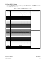
LIST OF ILLUSTRATIONS
(Continued)
Title
Figure
A-2
A-3
A-4
A-5
A-6
A-7
A-8
A-9
A-10
A-11
A-12
A-13
A-14
A-15
A-16
A-17
A-18
A-19
A-20
A-21
A-22
A-23
A-24
A-25
A-26
A-27
A-28
A-29
A-30
A-31
A-32
A-33
A-34
A-35
A-36
A-37
B-1
B-2
B-3
D-1
Page
External Clock Input Timing Diagram ........................................................... A-11
ECLK Output Timing Diagram ...................................................................... A-11
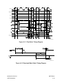
Read Cycle Timing Diagram ........................................................................ A-12
Write Cycle Timing Diagram ......................................................................... A-13
Fast Termination Read Cycle Timing Diagram ............................................ A-14
Fast Termination Write Cycle Timing Diagram ............................................. A-15
Bus Arbitration Timing Diagram — Active Bus Case ................................... A-16
Bus Arbitration Timing Diagram — Idle Bus Case ....................................... A-17
Show Cycle Timing Diagram ........................................................................ A-18
Chip-Select Timing Diagram ........................................................................ A-19
Reset and Mode Select Timing Diagram ...................................................... A-19
Background Debug Mode Timing Diagram (Serial Communication) ............ A-20
Background Debug Mode Timing Diagram (Freeze Assertion) .................... A-21
ECLK Timing Diagram .................................................................................. A-22
QSPI Timing — Master, CPHA = 0 .............................................................. A-24
QSPI Timing — Master, CPHA = 1 .............................................................. A-24
QSPI Timing — Slave, CPHA = 0 ................................................................ A-25
QSPI Timing — Slave, CPHA = 1 ................................................................ A-25
SPI Timing — Master, CPHA = 0 ................................................................. A-27
SPI Timing — Master, CPHA = 1 ................................................................. A-27
SPI Timing — Slave, CPHA = 0 ................................................................... A-28
SPI Timing — Slave, CPHA = 1 ................................................................... A-28
Input Signal Conditioner Timing ................................................................... A-29
Pulse Accumulator — Event Counting Mode (Leading Edge) ...................... A-30
Pulse Accumulator — Gated Mode (Count While Pin High) ........................ A-31
Pulse Accumulator — Using TOF as Gated Mode Clock ............................. A-32
PWMx (PWMx Register = 01, Fast Mode) ................................................... A-32
Output Compare (Toggle Pin State) ............................................................. A-33
Input Capture (Capture on Rising Edge) ...................................................... A-34
General-Purpose Input ................................................................................. A-35
General-Purpose Output (Causes Input Capture) ........................................ A-36
Force Compare (CLEAR) ............................................................................. A-37
8-Bit ADC Conversion Accuracy .................................................................. A-41
10-Bit ADC Conversion Accuracy ................................................................ A-42
Programming Voltage Envelope ................................................................... A-44
VFPE Conditioning Circuit ............................................................................. A-44
MC68HC16Y3 Pin Assignment for 160-Pin Package ..................................... B-2
MC68HC916Y3 Pin Assignment for 160-Pin Package ................................... B-3
160-Pin Package Dimensions ........................................................................ B-4
CPU16 Register Model ...................................................................................D-2
MOTOROLA
xx
MC68HC16Y3/916Y3
USER’S MANUAL
LIST OF TABLES
Table
1-1
3-1
3-2
3-3
4-2
4-3
4-4
4-5
4-6
4-7
5-1
5-2
5-3
5-4
5-5
5-6
5-7
5-8
5-9
5-10
5-11
5-12
5-13
5-14
5-15
5-16
5-17
5-18
5-19
5-20
5-21
5-22
5-23
5-24
5-25
5-26
5-27
5-28
5-29
5-30
6-1
Title
Page
MC68HC16Y3/916Y3 Modules ....................................................................... 1-1
MC68HC16Y3/MC68HC916Y3 Pin Characteristics ........................................ 3-8
MC68HC16Y3/MC68HC916Y3 Driver Types................................................ 3-12
MC68HC16Y3/MC68HC916Y3 Pin Functions .............................................. 3-13
Instruction Set Summary ............................................................................... 4-12
Instruction Set Abbreviations and Symbols................................................... 4-30
CPU16 Implementation of M68HC11 CPU Instructions ................................ 4-32
Exception Vector Table ................................................................................. 4-38
IPIPE0/IPIPE1 Encoding ............................................................................... 4-41
Command Summary ..................................................................................... 4-43
Show Cycle Enable Bits .................................................................................. 5-4
16.78 MHz Clock Control Multipliers ............................................................. 5-10
16.78 MHz System Clock Frequencies ......................................................... 5-12
Bus Monitor Period........................................................................................ 5-17
MODCLK Pin and SWP Bit During Reset ..................................................... 5-18
Software Watchdog Divide Ratio................................................................... 5-19
MODCLK Pin and PTP Bit at Reset .............................................................. 5-20
Periodic Interrupt Priority............................................................................... 5-21
Size Signal Encoding .................................................................................... 5-24
Address Space Encoding .............................................................................. 5-24
Effect of DSACK Signals ............................................................................... 5-26
Operand Alignment ....................................................................................... 5-28
DSACK, BERR, and HALT Assertion Results............................................... 5-36
Reset Source Summary ................................................................................ 5-41
Basic Configuration Options.......................................................................... 5-42
Bus and Port Configuration Options.............................................................. 5-42
16-Bit Expanded Mode Reset Configuration ................................................. 5-46
8-Bit Expanded Mode Reset Configuration ................................................... 5-47
Single-Chip Mode Reset Configuration ......................................................... 5-48
Module Pin Functions.................................................................................... 5-50
SCIM2 Pin Reset States................................................................................ 5-52
Chip-Select Pin Functions ............................................................................. 5-63
Pin Assignment Field Encoding..................................................................... 5-64
Block Size Encoding...................................................................................... 5-65
Chip-Select Base and Option Register Reset Values ................................... 5-69
CSBOOT Base and Option Register Reset Values....................................... 5-70
General-Purpose I/O Ports............................................................................ 5-70
Port E Pin Assignments................................................................................. 5-72
Port F Pin Assignments................................................................................. 5-73
PFPAR Pin Functions.................................................................................... 5-74
SRAM Array Address Space Type .................................................................. 6-2
MC68HC16Y3/916Y3
USER’S MANUAL
MOTOROLA
xxi
LIST OF TABLES
(Continued)
Title
Table
7-1
7-2
9-1
9-2
10-1
10-2
10-3
10-4
10-5
10-6
10-7
10-8
10-9
10-10
10-11
11-1
11-2
11-3
11-4
11-5
12-1
12-2
12-3
12-4
12-5
12-6
12-7
14-1
14-2
14-3
14-4
14-5
A-1
A-2
A-3
A-4
A-5
A-6
A-7
A-8
A-9
Page
ROM Array Space Field .................................................................................. 7-2
Wait States Field ............................................................................................. 7-3
Bootstrap Vector Assignments ........................................................................ 9-3
TPUFLASH Erase Operation Address Ranges............................................... 9-4
FRZ Field Selection....................................................................................... 10-4
Multiplexer Channel Sources ........................................................................ 10-5
Prescaler Output ........................................................................................... 10-7
Sample Time Selection ................................................................................. 10-7
Conversion Parameters Controlled by ADCTL1............................................ 10-8
ADC Conversion Modes................................................................................ 10-8
Single-Channel Conversions (MULT = 0).................................................... 10-10
Multiple-Channel Conversions (MULT = 1) ................................................. 10-11
Result Register Formats.............................................................................. 10-14
External Circuit Settling Time (10-Bit Conversions) .................................... 10-24
Error Resulting From Input Leakage (IOFF)................................................ 10-24
Effect of DDRQS on QSM Pin Function ........................................................ 11-5
QSPI Pins...................................................................................................... 11-9
Bits Per Transfer ......................................................................................... 11-19
Serial Frame Formats.................................................................................. 11-27
Effect of Parity Checking on Data Size ....................................................... 11-28
MCCI Interrupt Vectors.................................................................................. 12-3
Pin Assignments............................................................................................ 12-4
SPI Pin Functions.......................................................................................... 12-7
SCK Frequencies ........................................................................................ 12-11
SCI Pins ...................................................................................................... 12-18
Serial Frame Formats.................................................................................. 12-19
Effect of Parity Checking on Data Size ....................................................... 12-20
TCR1 Prescaler Control Bits ....................................................................... 14-14
TCR2 Counter Clock Source....................................................................... 14-15
TCR2 Prescaler Control .............................................................................. 14-16
TPU2 Function Encodings........................................................................... 14-17
Channel Priority Encodings ......................................................................... 14-18
Maximum Ratings............................................................................................ A-1
Typical Ratings................................................................................................ A-2
Thermal Characteristics .................................................................................. A-3
Clock Control Timing ....................................................................................... A-4
DC Characteristics .......................................................................................... A-5
AC Timing........................................................................................................ A-8
16.78 MHz Background Debug Mode Timing ............................................... A-20
ECLK Bus Timing .......................................................................................... A-21
QSPI Timing .................................................................................................. A-23
MOTOROLA
xxii
MC68HC16Y3/916Y3
USER’S MANUAL
LIST OF TABLES
(Continued)
Title
Table
A-10
A-11
A-12
A-13
A-14
A-15
A-16
A-17
D-1
D-2
D-3
D-4
D-5
D-6
D-7
D-8
D-9
D-10
D-11
D-12
D-13
D-14
D-15
D-16
D-17
D-18
D-19
D-20
D-21
D-22
D-23
D-24
D-25
D-26
D-27
D-29
D-30
D-31
D-32
D-33
D-34
Page
SPI Timing..................................................................................................... A-26
General Purpose Timer AC Characteristics .................................................. A-29
ADC Maximum Ratings ................................................................................. A-38
ADC DC Electrical Characteristics (Operating) ............................................. A-39
ADC AC Characteristics (Operating)............................................................. A-39
ADC Conversion Characteristics (Operating)................................................ A-40
TPUFLASH/Flash EEPROM Module Specifications ..................................... A-43
TPUFLASH/Flash EEPROM Module Life...................................................... A-43
Module Address Map ......................................................................................D-1
SCIM2 Address Map .......................................................................................D-4
Show Cycle Enable Bits ..................................................................................D-6
Port E Pin Assignments.................................................................................D-11
Port F Pin Assignments.................................................................................D-13
Software Watchdog Divide Ratio...................................................................D-14
Bus Monitor Timeout Period..........................................................................D-15
Pin Assignment Field Encoding.....................................................................D-18
CSPAR0 Pin Assignments ............................................................................D-18
CSPAR1 Pin Assignments ............................................................................D-19
Reset Pin Function of CS[10:6] .....................................................................D-19
Block Size Field Bit Encoding........................................................................D-20
BYTE Field Bit Encoding ...............................................................................D-21
Read/Write Field Bit Encoding ......................................................................D-21
DSACK Field Encoding .................................................................................D-22
Address Space Bit Encodings .......................................................................D-23
Interrupt Priority Level Field Encoding ..........................................................D-23
SRAM Address Map......................................................................................D-25
SRAM Array Address Space Type ................................................................D-25
MRM Address Map........................................................................................D-27
ROM Array Space Field ................................................................................D-28
Wait States Field ...........................................................................................D-28
Flash EEPROM Address Map.......................................................................D-31
Array Space Encoding...................................................................................D-33
Wait State Encoding......................................................................................D-34
Bootstrap Words............................................................................................D-36
ADC Module Address Map............................................................................D-37
Sample Time Selection .................................................................................D-39
Prescaler Output ...........................................................................................D-40
ADC Conversion Mode..................................................................................D-41
Single-Channel Conversions (MULT = 0)......................................................D-42
Multiple-Channel Conversions (MULT = 1) ...................................................D-43
QSM Address Map ........................................................................................D-46
MC68HC16Y3/916Y3
USER’S MANUAL
MOTOROLA
xxiii
LIST OF TABLES
(Continued)
Title
Table
D-35
D-36
D-37
D-38
D-39
D-40
D-41
D-42
D-43
D-44
D-45
D-46
D-47
D-48
D-49
D-50
D-51
D-52
D-54
D-55
D-56
D-57
D-58
D-59
D-60
D-61
D-62
D-63
D-64
14-7
Page
Examples of SCI Baud Rates........................................................................D-49
PQSPAR Pin Assignments............................................................................D-53
Effect of DDRQS on QSM Pin Function ........................................................D-54
Bits Per Transfer ...........................................................................................D-55
Examples of SCK Frequencies .....................................................................D-56
MCCI Address Map .......................................................................................D-62
Interrupt Vector Sources ...............................................................................D-64
MPAR Pin Assignments ................................................................................D-65
Effect of MDDR on MCCI Pin Function .........................................................D-66
Examples of SCI Baud Rates........................................................................D-68
GPT Address Map.........................................................................................D-75
GPT Interrupt Sources ..................................................................................D-77
PAMOD and PEDGE Effects.........................................................................D-79
PACLK[1:0] Effects........................................................................................D-79
OM/OL[5:2] Effects........................................................................................D-80
EDGE[4:1] Effects .........................................................................................D-80
CPR[2:0]/Prescaler Select Field....................................................................D-81
PPR[2:0] Field ...............................................................................................D-83
TPU2 Register Map.......................................................................................D-86
TCR1 Prescaler Control Bits .........................................................................D-87
TCR2 Prescaler Control Bits .........................................................................D-88
FRZ[1:0] Encoding ........................................................................................D-90
Breakpoint Enable Bits ..................................................................................D-90
Channel Priorities ..........................................................................................D-94
Entry Table Bank Location ............................................................................D-95
System Clock Frequency/Minimum Guaranteed Detected Pulse .................D-96
Parameter RAM Address Map ......................................................................D-97
TPUFLASH Address Map .............................................................................D-98
Array Space Encoding.................................................................................D-100
TPUFLASH Erase Operation Address Ranges...........................................D-102
MOTOROLA
xxiv
MC68HC16Y3/916Y3
USER’S MANUAL
SECTION 1INTRODUCTION
The MC68HC16Y3 and the MC68HC916Y3 microcontrollers are high-speed 16-bit
control units that are upwardly code compatible with M68HC11 controllers. Both are
members of the M68HC16 Family of modular microcontrollers.
M68HC16 microcontroller units (MCUs) are built up from standard modules that interface via a common internal bus. Standardization facilitates rapid development of devices tailored for specific applications.
MC68HC16Y3 and the MC68HC916Y3 MCUs incorporate a number of different modules. Refer to Table 1-1 for information on the contents of a particular MCU. (X) indicates that the module is used in the MCU. All of these modules are interconnected by
the intermodule bus (IMB).
Table 1-1 MC68HC16Y3/916Y3 Modules
Modules
MC68HC16Y3
MC68HC916Y3
Central Processor Unit (CPU16)
X
X
Single-Chip Integration Module 2 (SCIM2)
X
X
Standby RAM (SRAM)
4K
2K
Masked ROM Module (MRM)
96K
—
Analog-to-Digital Converter (ADC)
X
X
Queued Serial Module (QSM)
X
X
Multichannel Communication Interface (MCCI)
X
X
General Purpose Timer (GPT)
X
X
Time Processor Unit 2 (TPU2)
X
X
TPU Flash EEPROM (TPUFLASH)
—
4K
Flash EEPROM Module (FLASH)
—
96K
The maximum system clock for MC68HC16Y3 and the MC68HC916Y3 MCUs is 16.78
MHz. An internal phase-locked loop circuit synthesizes the system clock from either a
slow (typically 32.768 kHz) or fast (typically 4.194 MHz) reference, or uses an external
frequency source. System hardware and software support changes in clock rate during operation. Because the MCUs are a fully static design, register and memory contents are not affected by clock rate changes.
High-density complementary metal-oxide semiconductor (HCMOS) architecture
makes the basic power consumption low. Power consumption can be minimized by
stopping the system clock. The M68HC16 instruction set includes a low-power stop
(LPSTOP) command that efficiently implements this capability.
MC68HC16Y3/916Y3
USER’S MANUAL
MOTOROLA
1-1
Documentation for the Modular Microcontroller Family follows the modular construction of the devices in the product line. Each device has a comprehensive user’s manual that provides sufficient information for normal operation of the device. The user’s
manual is supplemented by module reference manuals that provide detailed information about module operation and applications. Refer to Motorola publication Advanced
Microcontroller Unit (AMCU) Literature (BR1116/D) for a complete list of documentation to supplement this manual.
MOTOROLA
1-2
MC68HC16Y3/916Y3
USER’S MANUAL
SECTION 2NOMENCLATURE
The following tables show the nomenclature used throughout the MC68HC16Y3/
916Y3 User’s Manual.
2.1 Symbols and Operators
Symbol
MC68HC16Y3/916Y3
USER’S MANUAL
Function
+
Addition
-
Subtraction (two’s complement) or negation
∗
Multiplication
/
Division
>
Greater
<
Less
=
Equal
≥
Equal or greater
≤
Equal or less
≠
Not equal
•
AND
✛
Inclusive OR (OR)
⊕
Exclusive OR (EOR)
NOT
Complementation
:
Concatenation
⇒
Transferred
⇔
Exchanged
±
Sign bit; also used to show tolerance
«
Sign extension
%
Binary value
$
Hexadecimal value
MOTOROLA
2-1
2.2 CPU16 Register Mnemonics
MOTOROLA
2-2
Mnemonic
Register
A
Accumulator A
AM
Accumulator M
B
Accumulator B
CCR
Condition code register
D
Accumulator D
E
Accumulator E
EK
Extended addressing extension field
HR
MAC multiplier register
IR
MAC multiplicand register
IX
Index register X
IY
Index register Y
IZ
Index register Z
K
Address extension register
PC
Program counter
PK
Program counter extension field
SK
Stack pointer extension field
SP
Stack pointer
XK
Index register X extension field
YK
Index register Y extension field
ZK
Index register Z extension field
XMSK
Modulo addressing index register X mask
YMSK
Modulo addressing index register Y mask
S
LPSTOP mode control bit
MV
AM overflow flag
H
Half carry flag
EV
AM extended overflow flag
N
Negative flag
Z
Zero flag
V
Two’s complement overflow flag
C
Carry/borrow flag
IP
Interrupt priority field
SM
Saturation mode control bit
MC68HC16Y3/916Y3
USER’S MANUAL
2.3 Pin and Signal Mnemonics
Mnemonic
Register
ADDR[23:0]
Address bus
AN[7:0]
ADC Analog inputs
AS
Address strobe
BERR
Bus error
BG
Bus grant
BGACK
Bus grant acknowledge
BKPT
Breakpoint
BR
Bus request
CLKOUT
System clock
CS[10:5], CS3
Chip-selects
CSBOOT
Boot ROM chip-select
CSE
Emulation chip-select
CSM
Module chip-select
DATA[15:0]
Data bus
DS
Data strobe
DSACK[1:0]
Data and size acknowledge
DSCLK
Development serial clock
DSI
Development serial input
DSO
Development serial output
ECLK
6800 Bus clock
EXTAL
External crystal oscillator connection
FASTREF
Fast/slow reference select
FC[2:0]
Function codes
FREEZE
Freeze
HALT
Halt
IC[3:1]
GPT Input capture
IPIPE[1:0]
Instruction pipeline MUX
IRQ[7:1]
Interrupt request
MISO
Master in slave out
MOSI
Master out slave in
OC[5:1]
GPT Output compare
PA[7:0]
SCIM2 I/O port A
PADA[7:0]
ADC I/O port A
PAI
GPT Pulse accumulator input
PB[7:0]
SCIM2 I/O port B
PC[6:0]
SCIM2 I/O port C
PCLK
GPT External clock input
PCS[2:0]
QSPI Peripheral chip-selects
PE[7:0]
SCIM2 I/O port E
PF[7:0]
SCIM2 I/O port F
PG[7:0]
SCIM2 I/O port G
MC68HC16Y3/916Y3
USER’S MANUAL
MOTOROLA
2-3
Mnemonic
Register
PGP[7:0]
GPT I/O port
PH[7:0]
SCIM2 I/O port H
PQS[5:0]
QSM I/O port
PWMA
PWM Output A
PWMB
PWM Output B
QUOT
Quotient out
R/W
Read/Write
RESET
Reset
RXDA
SCI A Receive Data
RXDB
SCI B Receive Data
SCK
Serial clock (SPI)
SIZ[1:0]
Size
SS
Slave-select
TSC
Three-state control
TXDA
SCI A Transmit Data
TXDB
SCI B Transmit Data
VDDA/VSSA
A/D Converter power
VDDSYN/MODCLK/VSSSYN
Clock synthesizer power
VFPE
Flash EEPROM/TPU Flash EEPROM program/erase power
VRH/VRL
A/D Reference voltage
VSS/VDD
Microcontroller power
VSTBY
Standby RAM power
XFC
External filter capacitor connection
XTAL
External crystal oscillator connection
MOTOROLA
2-4
MC68HC16Y3/916Y3
USER’S MANUAL
2.4 Register Mnemonics
Mnemonic
Register
ADCMCR
ADC Module Configuration Register
ADTEST
ADC Test Register
ADCTL[0:1]
ADC Control Registers [0:1]
ADSTAT
ADC Status Register
CFORC
GPT Compare Force Register
CFSR[0:3]
TPU2 Channel Function Selection Registers [0:3]
CIER
TPU2 Channel Interrupt Enable Register
CISR
TPU2 Channel Interrupt Status Register
CPR[0:1]
TPU2 Channel Priority Registers [0:1]
CREG
SCIM2 Test Module Control Register
CR[0:F]
QSM Command RAM [0:F]
CSBARBT
SCIM2 Chip-Select Base Address Register Boot ROM
CSBAR[0:10]
SCIM2 Chip-Select Base Address Registers [0:10]
CSORBT
SCIM2 Chip-Select Option Register Boot ROM
CSOR[0:10]
SCIM2 Chip-Select Option Registers [0:10]
CSPAR[0:1]
SCIM2 Chip-Select Pin Assignment Registers [0:1]
DCNR
TPU2 Decoded Channel Number Register
DDRAB
SCIM2 Port A/B Data Direction Register
DDRE
SCIM2 Port E Data Direction Register
DDRF
SCIM2 Port F Data Direction Register
DDRG
SCIM2 Port G Data Direction Register
DDRGP
GPT Port GP Data Direction Register
DDRH
SCIM2 Port H Data Direction Register
DDRM
MCCI Data Direction Register
DDRQS
QSM Port QS Data Direction Register
DREG
SCIM2 Test Module Distributed Register
DSCR
TPU2 Development Support Control Register
DSSR
TPU2 Development Support Status Register
FEE[1:3]BAH
Flash EEPROM Base Address High Registers [1:3]
FEE[1:3]BAL
Flash EEPROM Base Address Low Registers [1:3]
FEE[1:3]BS[0:3]
Flash EEPROM [1:3] Bootstrap Words [0:3]
FEE[1:3]CTL
Flash EEPROM Control Registers [1:3]
FEE[1:3]MCR
Flash EEPROM Module Configuration Registers [1:3]
FEE[1:3]TST
Flash EEPROM Test Registers [1:3]
GPTMCR
GPT Module Configuration Register
GPTMTR
GPT Module Test Register
HSQR[0:1]
TPU2 Host Sequence Register [0:1]
HSRR[0:1]
TPU2 Host Service Request Register [0:1]
ICR
GPT Interrupt Configuration Register
ILSCI
MCCI SCI Interrupt Level Register
ILSPI
MCCI SPI Interrupt Level Register
MC68HC16Y3/916Y3
USER’S MANUAL
MOTOROLA
2-5
Mnemonic
Register
LR
TPU2 Link Register
LJSRR[0:7]
ADC Left-Justified Signed Result Registers [0:7]
LJURR[0:7]
ADC Left-Justified Unsigned Result Registers [0:7]
MIVR
MCCI Interrupt Vector Register
MMCR
MCCI Module Configuration Register
MPAR
MCCI Pin Assignment Register
MRMCR
Masked ROM Module Configuration Register
MTEST
MCCI Test Register
OC1D
GPT Output Compare 1 Action Data Register
OC1M
GPT Output Compare 1 Action Mask Register
PACNT
GPT Pulse Accumulator Counter Register
PACTL
GPT Pulse Accumulator Control Register
PEPAR
SCIM2 Port E Pin Assignment Register
PFIVR
SCIM2 Port F Edge Detect Interrupt Vector
PFLVR
SCIM2 Port F Edge Detect Interrupt Level
PFPAR
SCIM2 Port F Pin Assignment Register
PICR
SCIM2 Periodic Interrupt Control Register
PITR
SCIM2 Periodic Interrupt Timer Register
PORTA
SCIM2 Port A Data Register
PORTADA
ADC Port ADA Data Register
PORTB
SCIM2 Port B Data Register
PORTC
SCIM2 Port C Data Register
PORTE[0:1]
SCIM2 Port E Data Registers [0:1]
PORTF[0:1]
SCIM2 Port F Data Registers [0:1]
PORTG
SCIM2 Port G Data Register
PORTGP
GPT Port GP Data Register
PORTH
SCIM2 Port H Data Register
MOTOROLA
2-6
PORTF
SCIM2 Port F Data Register
PORTFE
SCIM2 Port F Edge Detect Flag
PORTMC
MCCI Port Data Register
PORTMCP
MCCI Port Pin State Register
PORTQS
QSM Port QS Data Register
PQSPAR
QSM Port QS Pin Assignment Register
PRESCL
GPT Prescaler Register
PWMA
GPT PWM Control Register A
PWMB
GPT PWM Control Register B
PWMBUFA
GPT PWM Buffer Register A
PWMBUFB
GPT PWM Buffer Register B
PWMC
GPT PWM Control Register C
PWMCNT
GPT PWM Counter Register
QILR
QSM Interrupt Level Register
QIVR
QSM Interrupt Vector Register
QSMCR
QSM Module Configuration Register
MC68HC16Y3/916Y3
USER’S MANUAL
Mnemonic
Register
QTEST
QSM Test Register
RAMBAH
RAM Array Base Address High Register
RAMBAL
RAM Array Base Address Low Register
RAMMCR
RAM Module Configuration Register
RAMTST
RAM Test Register
RJURR[0:7]
ADC Right-Justified Unsigned Result Registers [0:7]
ROMBAH
ROM Base Address High Register
ROMBAL
ROM Base Address Low Register
ROMBS[0:3]
ROM Bootstrap Words [0:3]
RR[0:F]
QSM Receive Data RAM [0:F]
RSR
SCIM2 Reset Status Register
SCCR[0:1]
QSM SCI Control Registers [0:1]
SCCR[0:1]
SCI Control Registers [0:1]
SCDR
QSM SCI Data Register
SCSR
QSM SCI Status Register
SCIM2CR
SCIM2 Module Configuration Register
SCIM2TR
SCIM2 Test Register
SCIM2TRE
SCIM2 Test Register (ECLK)
SIGHI
ROM Signature High Register
SIGLO
ROM Signature Low Register
SCCR0[A:B]
MCCI SCI Control 0 Registers [A:B]
SCCR1[A:B]
MCCI SCI Control 1 Registers [A:B]
SCDR[A:B]
MCCI SCI Data Registers [A:B]
SCDR
QSM SCI Data Register
SCSR[A:B]
MCCI SCI Status Registers [A:B]
SGLR
TPU2 Service Grant Latch Register
SPCR
MCCI SPI Control Register
SPDR
MCCI SPI Data Register
SPSR
QSM SPI Status Register
SPSR
MCCI SPI Status Register
SWSR
SCIM2 Software Watchdog Service Register
SYNCR
SCIM2 Clock Synthesizer Control Register
SYPCR
SCIM2 System Protection Control Register
TCNT
GPT Timer Counter Register
TCR
TPU2 Test Configuration Register
TCTL[1:2]
GPT Timer Control Registers [1:2]
TFBAH
TPUFLASH Base Address Register High
TFBAL
TPUFLASH Base Address Register Low
TFBS[0:3]
TPUFLASH Bootstrap Word [0:3]
TFCTL
TPUFLASH Control Register
TFLG[1:2]
GPT Timer Flag Registers [1:2]
TFMCR
TPUFLASH Module Configuration Register
TFTST
TPUFLASH Test Register
MC68HC16Y3/916Y3
USER’S MANUAL
MOTOROLA
2-7
MOTOROLA
2-8
Mnemonic
Register
TI4/O5
GPT Timer Input Capture 4/Output Compare 5 Register
TIC[1:3]
GPT Timer Input Capture Registers [1:3]
TICR
TPU2 Interrupt Configuration Register
TMSK[1:2]
GPT Timer Mask Register [1:2]
TOC[1:4]
GPT Timer Output Compare Registers [1:4]
TPUMCR
TPU2 Module Configuration Register
TPUMCR2
TPU Module Configuration Register 2
TR[0:F]
QSM Transmit RAM [0:F]
TSTMSRA
SCIM2 Test Master Shift Register A
TSTMSRB
SCIM2 Test Master Shift Register B
TSTRC
SCIM2 Test Repetition Count Register
TSTSC
SCIM2 Test Shift Count Register
MC68HC16Y3/916Y3
USER’S MANUAL
2.5 Conventions
Logic level one is the voltage that corresponds to a Boolean true (1) state.
Logic level zero is the voltage that corresponds to a Boolean false (0) state.
Set refers specifically to establishing logic level one on a bit or bits.
Clear refers specifically to establishing logic level zero on a bit or bits.
Asserted means that a signal is in active logic state. An active low signal changes
from logic level one to logic level zero when asserted, and an active high signal changes from logic level zero to logic level one.
Negated means that an asserted signal changes logic state. An active low signal
changes from logic level zero to logic level one when negated, and an active high signal changes from logic level one to logic level zero.
A specific mnemonic within a range is referred to by mnemonic and number. A15 is
bit 15 of Accumulator A; ADDR7 is line 7 of the address bus; CSOR0 is chip-select
option register 0. A range of mnemonics is referred to by mnemonic and the numbers
that define the range. VBR[4:0] are bits four to zero of the Vector Base Register;
CSOR[0:5] are the first six chip-select option registers.
Parentheses are used to indicate the content of a register or memory location, rather
than the register or memory location itself. For example, (A) is the content of Accumulator A. (M : M + 1) is the content of the word at address M.
LSB means least significant bit or bits. MSB means most significant bit or bits. References to low and high bytes are spelled out.
LSW means least significant word or words. MSW means most significant word or
words.
ADDR is the address bus. ADDR[7:0] are the eight LSB of the address bus.
DATA is the data bus. DATA[15:8] are the eight MSB of the data bus.
MC68HC16Y3/916Y3
USER’S MANUAL
MOTOROLA
2-9
MOTOROLA
2-10
MC68HC16Y3/916Y3
USER’S MANUAL
SECTION 3OVERVIEW
This section provides general information on MC68HC16Y3 and MC68HC916Y3
MCUs. It lists features of each of the modules, shows device functional divisions and
pinouts, summarizes signal and pin functions, discusses the intermodule bus, and provides system memory maps. Timing and electrical specifications for the entire microcontroller and for individual modules are provided in APPENDIX A ELECTRICAL
CHARACTERISTICS. Comprehensive module register descriptions and memory
maps are provided in APPENDIX D REGISTER SUMMARY.
3.1 MC68HC16Y3/916Y3 MCU Features
The following paragraphs highlight capabilities of each of the MCU modules. Each
module is discussed separately in a subsequent section of this manual.
3.1.1 Central Processing Unit (CPU16)
• 16-Bit architecture
• Full set of 16-bit instructions
• Three 16-bit index registers
• Two 16-bit accumulators
• Control-oriented digital signal processing capability
• Addresses up to 1 Mbyte of program memory; 1 Mbyte of data memory
• Background debug mode
• Fully static operation
3.1.2 Single-Chip Integration Module 2 (SCIM2)
• Single-chip and expanded operating modes
• External bus support in expanded mode
• Nine programmable chip-select outputs
• Phase-locked loop system clock with user-selectable fast or slow reference
• Watchdog timer, clock monitor, and bus monitor
• Address and data bus provide 32 discrete I/O lines in single-chip mode
• Enhanced reset controller
3.1.3 Standby RAM (SRAM)
• 4-Kbyte SRAM used by the MC68HC16Y3
• 2-Kbyte SRAM used by the MC68HC916Y3
• Standby voltage (VSTBY) input for low-power standby operation
• Power-down status flag denotes loss of VSTBY during low-power standby operation
MC68HC16Y3/916Y3
USER’S MANUAL
MOTOROLA
3-1
3.1.4 Masked ROM Module (MRM) — MC68HC16Y3 Only
• 96-Kbyte array, accessible as bytes or words
• User selectable default base address
• User selectable bootstrap ROM function
• User selectable ROM verification code
3.1.5 Flash EEPROM Module (FLASH) — MC68HC916Y3 Only
• 96 Kbytes, divided into three 32-Kbyte blocks
3.1.6 TPU Flash EEPROM Module (TPUFLASH) — MC68HC916Y3 Only
• 4-Kbytes
• Block-erasable; can be used for micro-ROM emulation or normal operation
3.1.7 Analog-to-Digital Converter (ADC)
• Eight channels, eight result registers, three result alignment modes
• Eight automated modes
3.1.8 Queued Serial Module (QSM)
• Queued serial peripheral interface
• Dual function I/O ports
3.1.9 Multichannel Communication Interface (MCCI)
• Two channels of enhanced SCI (UART)
3.1.10 General Purpose Timer (GPT)
• Two 16-bit free-running counters with one eight-stage prescaler
• Three input capture channels
• One input capture/output compare channel
• Four output compare channels
• One pulse accumulator/event counter input
• Two pulse width modulation outputs
• External clock input
3.1.11 Time Processor Unit 2 (TPU2)
• Sixteen channels, each associated with a pin
• Each channel can perform any time function
• Each channel can be programmed to perform match or capture operations with
one or both of the two 16-bit free running timer count registers (TCR1 and TCR2)
• Resolution is one-half that of the system clock period
MOTOROLA
3-2
MC68HC16Y3/916Y3
USER’S MANUAL
3.2 Intermodule Bus
The intermodule bus (IMB) is a standardized bus developed to facilitate the design of
modular microcontrollers. It contains circuitry that supports exception processing, address space partitioning, multiple interrupt levels, and vectored interrupts. The standardized modules in MC68HC16Y3 and MC68HC916Y3 MCUs communicate with
one another and external components via the IMB. Although the full IMB supports 24
address and 16 data lines, MC68HC16Y3 and MC68HC916Y3 MCUs use only 20 address lines. Because the CPU16 uses only 20 address lines. ADDR[23:20] follow the
state of ADDR19.
3.3 System Block Diagram and Pin Assignment Diagrams
Figures 3-1 and 3-2 show functional block diagrams of MC68HC16Y3 and
MC68HC916Y3 MCUs. Although diagram blocks represent the relative size of the
physical modules, there is not a one-to-one correspondence between location and
size of blocks in the diagram and location and size of integrated-circuit modules.
Figures 3-3 and 3-4 show MC68HC16Y3 and MC68HC916Y3 pin assignments based
on a 160-pin plastic surface-mount package. Refer to APPENDIX B MECHANICAL
DATA AND ORDERING INFORMATION for information on how to obtain package
dimensions. Refer to subsequent paragraphs in this section for pin and signal
descriptions.
MC68HC16Y3/916Y3
USER’S MANUAL
MOTOROLA
3-3
TXDA
RXDA
TXDB
RXDB
CSBOOT
CS[10:3]
96K
ROM
BR
BG
BGACK
PQS2/SCK
PORTQS
CONTROL
PQS4/PCS1
PQS3/PCS0/SS
PCS2
PCS0/SS
SCK
PQS1/MOSI
PGP2/IC3
ADDR[18:3]
32 K
OC4/OC1
PGP1/IC2
SIZ1
SIZ0
AS
DS
OC2/OC1
IC3
QSM
GPT
IC2
IC1
PGP0/IC1
DSACK1
DSACK0
CPU16
DATA[15:0]
AN7
AN6
AN5
AN4
AN3
AN2
AN1
AN0
CONTROL
PORT G/H
TPU2
R/W
RESET
HALT
BERR
IRQ[7:1]
FASTREF
CONTROL
PORT F
PORT ADA
CONTROL
AN7/PADA7
AN6/PADA6
AN5/PADA5
AN4/PADA4
AN3/PADA3
AN2/PADA2
AN1/PADA1
AN0/PADA0
4K
SRAM
VRH
CLOCK
VRL
PH[7:0]/DATA[7:0]
IRQ7/PF7
IRQ6/PF6
IRQ5/PF5
IRQ4/PF4
IRQ3/PF3
IRQ2/PF2
IRQ1/PF1
FASTREF/PF0
TSC
TEST
QUOT
FREEZE
CONTROL
CONTROL
T2CLK
TPUCH[15:0]
BKPT
IPIPE1
IPIPE0
DSI
DSO
DSCLK
PG[7:0]/DATA[15:8]
CLKOUT
XTAL
EXTAL
XFC
VDDSYN/MODCLK
VSSSYN
VSTBY
BKPT/DSCLK
IPIPE1/DSI
IPIPE0/DSO
SIZ1/PE7
SIZ0/PE6
AS/PE5
DS/PE4
DSACK1/PE1
DSACK0/PE0
IMB
ADC
PB[7:0]/ADDR[10:3]
EBI
OC3/OC1
OC1
PA[7:0]/ADDR[18:11]
ADDR[2:0]
IC4/OC5/OC1
PORT GP
CONTROL
PGP3/OC1
MCCI
MISO
ADDR23/CS10/ECLK
ADDR22/CS9/PC6
ADDR21/CS8/PC5
ADDR20/CS7/PC4
ADDR19/CS6/PC3
FC2/CS5/PC2
FC1/CS4/PC1
FC0/CS3/PC0
BR/CS0
BG/CSM
BGACK/CSE
ADDR[23:19]
PWMA
PWMB
PCLK
PAI
PGP6/OC4/OC1
PGP5/OC3/OC1
PGP4/OC2/OC1
64 K
MOSI
PQS0/MISO
PWMA
PWMB
PCLK
PAI
PGP7/IC4/OC5/OC1
SCIM2
PCS1
FC2
FC1
FC0
CONTROL
PORT E
PQS5/PCS2
CONTROL
PORT C
CHIP
SELECTS
CONTROL
PORT A/B
PORT MCCI
CONTROL
TXDA/PMC7
RXDA/PMC6
TXDB/PMC5
RXDB/PMC4
TSC
FREEZE/QUOT
MC68HC16Y3 BLOCK
Figure 3-1 MC68HC16Y3 Block Diagram
MOTOROLA
3-4
MC68HC16Y3/916Y3
USER’S MANUAL
VFPE2
TXDA
RXDA
TXDB
RXDB
CSBOOT
96K
FLASH
EEPROM
PQS2/SCK
PORTQS
CONTROL
PQS4/PCS1
PQS3/PCS0/SS
PCS2
PCS1
PCS0/SS
SCK
PQS1/MOSI
ADDR[18:3]
PWMA
PWMB
PCLK
PAI
32 K
SIZ1
SIZ0
AS
DS
PORT GP
CONTROL
OC3/OC1
OC2/OC1
IC3
PGP1/IC2
QSM
GPT
IC2
IC1
PGP0/IC1
DSACK1
DSACK0
TPU2
CPU16
DATA[15:0]
AN7
AN6
AN5
AN4
AN3
AN2
AN1
AN0
CONTROL
PORT G/H
4K
TPU
FLASH
EEPROM
R/W
RESET
HALT
BERR
IRQ[7:1]
FASTREF
CONTROL
PORT F
PORT ADA
CONTROL
AN7/PADA7
AN6/PADA6
AN5/PADA5
AN4/PADA4
AN3/PADA3
AN2/PADA2
AN1/PADA1
AN0/PADA0
4K
SRAM
VRH
CLOCK
VRL
VFPE1
PH[7:0]/DATA[7:0]
IRQ7/PF7
IRQ6/PF6
IRQ5/PF5
IRQ4/PF4
IRQ3/PF3
IRQ2/PF2
IRQ1/PF1
FASTREF/PF0
TSC
TEST
QUOT
FREEZE
CONTROL
CONTROL
T2CLK
TPUCH[15:0]
BKPT
IPIPE1
IPIPE0
DSI
DSO
DSCLK
PG[7:0]/DATA[15:8]
CLKOUT
XTAL
EXTAL
XFC
VDDSYN/MODCLK
VSSSYN
VSTBY
BKPT/DSCLK
IPIPE1/DSI
IPIPE0/DSO
SIZ1/PE7
SIZ0/PE6
AS/PE5
DS/PE4
DSACK1/PE1
DSACK0/PE0
IMB
ADC
PB[7:0]/ADDR[10:3]
EBI
OC4/OC1
OC1
PA[7:0]/ADDR[18:11]
ADDR[2:0]
IC4/OC5/OC1
PGP6/OC4/OC1
PGP2/IC3
MCCI
32 K
ADDR23/CS10/ECLK
ADDR22/CS9/PC6
ADDR21/CS8/PC5
ADDR20/CS7/PC4
ADDR19/CS6/PC3
FC2/CS5/PC2
FC1/PC1
FC0/CS3/PC0
BR/CS0
BG/CSM
BGACK/CSE
ADDR[23:19]
MISO
PWMA
PWMB
PCLK
PAI
PGP7/IC4/OC5/OC1
PGP3/OC1
SCIM2
FC2
FC1
FC0
MOSI
PQS0/MISO
PGP5/OC3/OC1
PGP4/OC2/OC1
32 K
BR
BG
BGACK
CONTROL
PORT E
PQS5/PCS2
CS[10:3]
CONTROL
PORT C
CHIP
SELECTS
CONTROL
PORT A/B
PORT MCCI
CONTROL
TXDA/PMC7
RXDA/PMC6
TXDB/PMC5
RXDB/PMC4
TSC
FREEZE/QUOT
MC68HC916Y3 BLOCK
Figure 3-2 MC68HC916Y3 Block Diagram
MC68HC16Y3/916Y3
USER’S MANUAL
MOTOROLA
3-5
VDD
DATA0
DATA1
DATA2
DATA3
DATA4
DATA5
DATA6
DATA7
DATA8
DATA9
DATA10
VDD
VSS
DATA11
DATA12
DATA13
DATA14
DATA15
VSS
ADDR0
DSACK0/PE0
DSACK1/PE1
PCS1/PQS4
PCS2/PQS5
VDD
VSS
DS/PE4
AS/PE5
SIZ0/PE6
SIZ1/PE7
R/W
FASTREF/PF0
IRQ1/PF1
IRQ2/PF2
IRQ3/PF3
IRQ4/PF4
IRQ5/PF5
IRQ6/PF6
IRQ7/PF7
120
119
118
117
116
115
114
113
112
111
110
109
108
107
106
105
104
103
102
101
100
99
98
97
96
95
94
93
92
91
90
89
88
87
86
85
84
83
82
81
121
122
123
124
125
126
127
128
129
130
131
132
133
134
135
136
137
138
139
140
141
142
143
144
145
146
147
148
149
150
151
152
153
154
155
156
157
158
159
160
80
79
78
77
76
75
74
73
72
71
70
69
68
67
66
65
64
63
62
61
60
59
58
57
56
55
54
53
52
51
50
49
48
47
46
45
44
43
42
41
MC68HC16Y3
MMMMM1
ATWLYYWW2
TSC
FREEZE/QUOT
BERR
HALT
RESET
VSS
CLKOUT
VSS
VDD
XFC
VDD
VSSSYN
EXTAL
VDDSYN/MODCLK
XTAL
VSTBY
NC
T2CLK
TPUCH15
TPUCH14
TPUCH13
TPUCH12
VSS
VDD
TPUCH11
TPUCH10
TPUCH9
TPUCH8
TPUCH7
TPUCH6
TPUCH5
TPUCH4
VSS
VDD
TPUCH3
TPUCH2
TPUCH1
TPUCH0
RXDB/PMC4
VSS
VRH
AN5/PADA5
AN4/PADA4
AN3/PADA3
AN2/PADA2
AN1/PADA1
AN0/PADA0
VSSA
VDDA
VDD
VSS
ADDR1
ADDR2
ADDR3
ADDR4
ADDR5
ADDR6
ADDR7
ADDR8
ADDR9
VSS
ADDR10
ADDR11
ADDR12
ADDR13
VDD
VSS
ADDR14
ADDR15
ADDR16
ADDR17
ADDR18
SS/PCS0/PQS3
MOSI/PQS1
MISO/PQS0
SCK/PQS2
TXDA/PMC7
RXDA/PMC6
TXDB/PMC5
VDD
1
2
3
4
5
6
7
8
9
10
11
12
13
14
15
16
17
18
19
20
21
22
23
24
25
26
27
28
29
30
31
32
33
34
35
36
37
38
39
40
VSS
CSBOOT
BR/CS0
BG/CSM
BGACK/CSE
FC0/CS3
FC1/CS4
FC2/CS5
VSS
VDD
ADDR19/CS6
ADDR20/CS7
ADDR21/CS8
ADDR22/CS9
ADDR23/CS10
VDD
VSS
NC
BKPT/DSCLK
IPIPE1/DSI
IPIPE0/DSO
VSS
VDD
PCLK
PWMB
PWMA
PAI
PGP7/IC4/OC5/OC1
PGP6/OC4/OC1
PGP5/OC3/OC1
PGP4/OC2/OC1
PGP3/OC1
PGP2/IC3
PGP1/IC2
PGP0/IC1
VSS
VDD
AN7/PADA7
AN6/PADA6
VRL
NOTES:
1. MMMMM = MASK OPTION NUMBER
2. ATWLYYWW = ASSEMBLY TEST LOCATION/YEAR, WEEK
MC68HC16Y3 160-PIN QFP
Figure 3-3 MC68HC16Y3 Pin Assignment for 160-Pin Package
MOTOROLA
3-6
MC68HC16Y3/916Y3
USER’S MANUAL
VDD
DATA0
DATA1
DATA2
DATA3
DATA4
DATA5
DATA6
DATA7
DATA8
DATA9
DATA10
VDD
VSS
DATA11
DATA12
DATA13
DATA14
DATA15
VSS
ADDR0
DSACK0/PE0
DSACK1/PE1
PCS1/PQS4
PCS2/PQS5
VDD
VSS
DS/PE4
AS/PE5
SIZ0/PE6
SIZ1/PE7
R/W
FASTREF/PF0
IRQ1/PF1
IRQ2/PF2
IRQ3/PF3
IRQ4/PF4
IRQ5/PF5
IRQ6/PF6
IRQ7/PF7
120
119
118
117
116
115
114
113
112
111
110
109
108
107
106
105
104
103
102
101
100
99
98
97
96
95
94
93
92
91
90
89
88
87
86
85
84
83
82
81
121
122
123
124
125
126
127
128
129
130
131
132
133
134
135
136
137
138
139
140
141
142
143
144
145
146
147
148
149
150
151
152
153
154
155
156
157
158
159
160
80
79
78
77
76
75
74
73
72
71
70
69
68
67
66
65
64
63
62
61
60
59
58
57
56
55
54
53
52
51
50
49
48
47
46
45
44
43
42
41
MC68HC916Y3
MMMMM1
ATWLYYWW2
TSC
FREEZE/QUOT
BERR
HALT
RESET
VSS
CLKOUT
VSS
VDD
XFC
VDD
VSSSYN
EXTAL
VDDSYN/MODCLK
XTAL
VSTBY
VFPE1
T2CLK
TPUCH15
TPUCH14
TPUCH13
TPUCH12
VSS
VDD
TPUCH11
TPUCH10
TPUCH9
TPUCH8
TPUCH7
TPUCH6
TPUCH5
TPUCH4
VSS
VDD
TPUCH3
TPUCH2
TPUCH1
TPUCH0
RXDB/PMC4
VSS
VRH
AN5/PADA5
AN4/PADA4
AN3/PADA3
AN2/PADA2
AN1/PADA1
AN0/PADA0
VSSA
VDDA
VDD
VSS
ADDR1
ADDR2
ADDR3
ADDR4
ADDR5
ADDR6
ADDR7
ADDR8
ADDR9
VSS
ADDR10
ADDR11
ADDR12
ADDR13
VDD
VSS
ADDR14
ADDR15
ADDR16
ADDR17
ADDR18
SS/PCS0/PQS3
MOSI/PQS1
MISO/PQS0
SCK/PQS2
TXDA/PMC7
RXDA/PMC6
TXDB/PMC5
VDD
1
2
3
4
5
6
7
8
9
10
11
12
13
14
15
16
17
18
19
20
21
22
23
24
25
26
27
28
29
30
31
32
33
34
35
36
37
38
39
40
VSS
CSBOOT
BR/CS0
BG/CSM
BGACK/CSE
FC0/CS3
FC1
FC2/CS5
VSS
VDD
ADDR19/CS6
ADDR20/CS7
ADDR21/CS8
ADDR22/CS9
ADDR23/CS10
VDD
VSS
VFPE2
BKPT/DSCLK
IPIPE1/DSI
IPIPE0/DSO
VSS
VDD
PCLK
PWMB
PWMA
PAI
PGP7/IC4/OC5/OC1
PGP6/OC4/OC1
PGP5/OC3/OC1
PGP4/OC2/OC1
PGP3/OC1
PGP2/IC3
PGP1/IC2
PGP0/IC1
VSS
VDD
AN7/PADA7
AN6/PADA6
VRL
NOTES:
1. MMMMM = MASK OPTION NUMBER
2. ATWLYYWW = ASSEMBLY TEST LOCATION/YEAR, WEEK
MC68HC916Y3 160-PIN QFP
Figure 3-4 MC68HC916Y3 Pin Assignment for 160-Pin Package
MC68HC16Y3/916Y3
USER’S MANUAL
MOTOROLA
3-7
3.4 Pin Descriptions
Table 3-1 summarizes pin characteristics of the MC68HC16Y3 and MC68HC916Y3
MCUs. Entries in the “Associated Module” column indicate to which module individual
pins belong. For MCU pins that can be outputs, the “Driver Type” column lists which
output driver type is used. Table 3-2 briefly describes the four primary driver types. A
“—” in the “Driver Type” column indicates either that the pin is an input only, and thus
does not have a driver, or that the pin has a special driver, like the XTAL pin. Entries
in the “Synchronized Input” and “Input Hysteresis” columns denote whether MCU pins
that can be inputs are synchronized to the system clock and if they have hysteresis.
Pins that are outputs only or that have special characteristics, like the EXTAL pin, have
a “—” in these columns.
Table 3-1 MC68HC16Y3/MC68HC916Y3 Pin Characteristics
Pin
Mnemonic(s)
Pin
Number(s)
Associated
Module
Driver
Type
Synchronized
Input
Input
Hysteresis
ADDR0
ADDR1
ADDR2
100
12
13
SCIM2
A
—
—
ADDR3/PB0
ADDR4/PB1
ADDR5/PB2
ADDR6/PB3
ADDR7/PB4
ADDR8/PB5
ADDR9/PB6
ADDR10/PB7
14
15
16
17
18
19
20
21
SCIM2
A
Y
Y
ADDR11/PA0
ADDR12/PA1
ADDR13/PA2
ADDR14/PA3
ADDR15/PA4
ADDR16/PA5
ADDR17/PA6
ADDR18/PA7
23
24
25
28
29
30
31
32
SCIM2
A
Y
Y
ADDR19/CS6/PC3
ADDR20/CS7/PC4
ADDR21/CS8/PC5
ADDR22/CS9/PC6
131
132
133
134
SCIM2
A
—
—
ADDR23/CS10/ECLK
135
SCIM2
A
—
—
AN0/PADA0
AN1/PADA1
AN2/PADA2
AN3/PADA3
AN4/PADA4
AN5/PADA5
AN6/PADA6
AN7/PADA7
7
6
5
4
3
2
159
158
ADC
—
Y1
Y
AS/PE5
92
SCIM2
B
Y
Y
N
BERR
78
SCIM2
—
Y2
BG/CSM
124
SCIM2
B
—
—
BGACK/CSE
125
SCIM2
B
Y
N
MOTOROLA
3-8
MC68HC16Y3/916Y3
USER’S MANUAL
Table 3-1 MC68HC16Y3/MC68HC916Y3 Pin Characteristics
Pin
Mnemonic(s)
Pin
Number(s)
Associated
Module
Driver
Type
Synchronized
Input
Input
Hysteresis
BKPT/DSCLK
139
CPU16
—
Y
Y
BR/CS0
123
SCIM2
B
Y
N
CLKOUT
74
SCIM2
A
—
—
CSBOOT
122
SCIM2
B
—
—
DATA0/PH0
DATA1/PH1
DATA2/PH2
DATA3/PH3
DATA4/PH4
DATA5/PH5
DATA6/PH6
DATA7/PH7
119
118
117
116
115
114
113
112
SCIM2
Aw
Y3
Y
DATA8/PG0
DATA9/PG1
DATA10/PG2
DATA11/PG3
DATA12/PG4
DATA13/PG5
DATA14/PG6
DATA15/PG7
111
110
109
106
105
104
103
102
SCIM2
Aw
Y3
Y
DS/PE4
93
SCIM2
B
Y
Y
DSACK0/PE0
DSACK1/PE1
99
98
SCIM2
B
Y
N
EXTAL4
68
SCIM2
—
—
—
B
Y1
Y
FASTREF/PF0
88
SCIM2
FC0/CS3/PC0
126
SCIM2
A
—
—
FC1/CS4/PC15
127
SCIM2
A
—
—
FC2/CS5/PC2
128
SCIM2
A
—
—
FREEZE/QUOT
79
CPU16
A
—
—
IC4/OC5/OC1/PGP7
148
GPT
A
Y
Y
IC3/PGP2
IC2/PGP1
IC1/PGP0
153
154
155
GPT
A
Y
Y
HALT
77
SCIM2
Bo
Y2
N
IPIPE0/DSO
141
CPU16
A
—
—
IPIPE1/DSI
140
CPU16
A
Y
Y
IRQ1/PF1
IRQ2/PF2
IRQ3/PF3
IRQ4/PF4
IRQ5/PF5
IRQ6/PF6
IRQ7/PF7
87
86
85
84
83
82
81
SCIM2
B
Y
Y
MISO/PQS0
35
QSM
Bo
Y1
Y
MOSI/PQS1
34
QSM
Bo
Y1
Y
MC68HC16Y3/916Y3
USER’S MANUAL
MOTOROLA
3-9
Table 3-1 MC68HC16Y3/MC68HC916Y3 Pin Characteristics
Pin
Mnemonic(s)
Pin
Number(s)
Associated
Module
Driver
Type
Synchronized
Input
Input
Hysteresis
OC4/OC1/PGP6
OC3/OC1/PGP5
OC2/OC1/PGP4
OC1/PGP3
149
150
151
152
GPT
A
Y
Y
PAI6
147
GPT
—
Y
Y
PCLK6
144
GPT
—
Y
Y
PCS2/PQS2
PCS1/PQS1
96
97
QSM
—
Y
Y
PWMA7
PWMB7
146
145
GPT
—
Y
Y
R/W
89
SCIM2
A
—
—
RESET
76
SCIM2
Bo
Y
Y
RXDA/PMC6
RXDB/PMC4
38
42
MCCI
Bo
Y1
Y
SS/PCS0/PQS3
33
QSM
Bo
Y
Y
Y
SCK/PQS2
36
QSM
Bo
Y1
SIZ0/PE6
SIZ1/PE7
91
90
SCIM2
B
Y
Y
T2CLK
63
TPU2
—
Y
Y
TPUCH0
TPUCH1
TPUCH2
TPUCH3
TPUCH4
TPUCH5
TPUCH6
TPUCH7
TPUCH8
TPUCH9
TPUCH10
TPUCH11
TPUCH12
TPUCH13
TPUCH14
TPUCH15
43
44
45
46
49
50
51
52
53
54
55
56
59
60
61
62
TPU2
A
Y
Y
TSC
80
SCIM2
—
Y
Y
TXDA/PMC7
TXDB/PMC5
37
39
MCCI
Bo
Y1
Y
MOTOROLA
3-10
MC68HC16Y3/916Y3
USER’S MANUAL
Table 3-1 MC68HC16Y3/MC68HC916Y3 Pin Characteristics
Pin
Mnemonic(s)
Pin
Number(s)
Associated
Module
Driver
Type
Synchronized
Input
Input
Hysteresis
VDD
10
26
40
47
57
70
72
95
108
120
130
136
143
157
—
—
—
—
VDDA
9
ADC
—
—
—
VDDSYN/MODCLK
67
SCIM2
—
—
—
VFPE1
64
TPUFLASH
—
—
—
VFPE2
138
FLASH1
FLASH2
FLASH3
—
—
—
VRH
VRL
1
160
ADC
—
—
—
VSS
11
21
27
41
48
58
73
75
94
101
107
121
129
137
142
156
—
—
—
—
VSSA
8
ADC
—
—
—
VSSSYN
69
SCIM2
—
—
—
VSTBY
65
SRAM
—
—
—
XFC4
71
SCIM2
—
—
—
66
SCIM2
—
—
—
4
XTAL
NOTES:
1. AN[7:0]/PADA[7:0], FASTREF/PF0, MISO/PQS0, MOSI/PQS1, SCK/PQS2, SS/PQS3, RXDB/PMC4, TXDB/
PMC5, RXDA/PMC6, and TXDA/PMC7 inputs are only synchronized when used as discrete general purpose
inputs.
2. BERR is only synchronized when executing retry or late bus cycle operations. HALT is only synchronized when
executing retry or single-step bus cycle operations. These uses of HALT and BERR are only supported on the
CPU32 and not the CPU16.
MC68HC16Y3/916Y3
USER’S MANUAL
MOTOROLA
3-11
3. DATA[15:8]/PG[7:0] and DATA[7:0]/PH[7:0] are only synchronized during reset and when being used as discrete
general purpose inputs.
4. EXTAL, XFC, and XTAL are clock connections.
5. CS4 is used only on the MC68HC16Y3.
6. PAI and PCLK can be used for discrete input, but are not part of an I/O port.
7. PWMA and PWMB can be used for discrete input, but are not part of an I/O port.
Table 3-2 MC68HC16Y3/MC68HC916Y3 Driver Types
Type
I/O
Description
A
O
Three-state capable output signals
Aw
O
Type A output with weak p-channel pullup during reset
B
O
Three-state output that includes circuitry to pull up output before high impedance is established,
to ensure rapid rise time
Bo
O
Type B output that can be operated in an open-drain mode
3.5 Signal Descriptions
Table 3-3 summarizes pin functions of the MC68HC16Y3 and MC68HC916Y3 MCUs.
Entries in the “Active State(s)” column denote the polarity of each MCU pin in its active
state. Some MCU pins have multiple functions and thus have multiple entries in the
“Active State(s)” column. For example, the ADDR23/CS10/ECLK pin can be programmed to be either address line 23 (ADDR23), chip-select output 10 (CS10), or the
M6800 bus clock (ECLK). Its entry in the “Active State(s)” column is “—/0/—” which
indicates the following:
• When programmed as ADDR23, the pin has no active state (“—”); it conveys information when driven by the MCU to logic 0 or logic 1.
• When programmed as CS10, the pin is active when driven to logic 0 (“0”) by the
MCU. When driven to logic 1, the chip-select function is inactive.
• When programmed as ECLK, the pin has no active state (“—”). M6800 bus devices drive or prepare to latch an address when ECLK is logic 0 and drive or prepare to latch data when ECLK is logic 1.
The “Discrete I/O Use” column indicates whether each pin can be used as a general
purpose input, output, or both. Those pins that cannot be used for general purpose I/
O will have a “—” in this column.
MOTOROLA
3-12
MC68HC16Y3/916Y3
USER’S MANUAL
Table 3-3 MC68HC16Y3/MC68HC916Y3 Pin Functions
Discrete
I/O Use
Pin
Mnemonic(s)
Pin
Number(s)
Active
State(s)
Associated
Module
ADDR0
ADDR1
ADDR2
100
12
13
—
SCIM2
Address lines [2:0].
—
ADDR3/PB0
ADDR4/PB1
ADDR5/PB2
ADDR6/PB3
ADDR7/PB4
ADDR8/PB5
ADDR9/PB6
ADDR10/PB7
14
15
16
17
18
19
20
21
—/—
SCIM2
Address lines [10:3] or digital I/O port B
[7:0].
I/O
ADDR11/PA0
ADDR12/PA1
ADDR13/PA2
ADDR14/PA3
ADDR15/PA4
ADDR16/PA5
ADDR17/PA6
ADDR18/PA7
23
24
25
28
29
30
31
32
—/—
SCIM2
Address lines [18:11] or digital I/O port
A [7:0].
I/O
ADDR19/CS6/PC3
ADDR20/CS7/PC4
ADDR21/CS8/PC5
ADDR22/CS9/PC6
131
132
133
134
—/0/—
SCIM2
Address lines [22:19], chip-select outputs [9:6], or digital output port C [6:3].
O
ADDR23/CS10/ECLK
135
—/0/—
SCIM2
Address line 23, chip-select output 10,
or E clock output for M6800 bus devices.
—
AN0/PADA0
AN1/PADA1
AN2/PADA2
AN3/PADA3
AN4/PADA4
AN5/PADA5
AN6/PADA6
AN7/PADA7
7
6
5
4
3
2
159
158
—/—
ADC
AS/PE5
92
0/—
SCIM2
Indicates that a valid address is on the
address bus or digital I/O port E5.
I/O
BERR
78
0
SCIM2
Requests a bus error exception.
—
BG/CSM
124
0/0
SCIM2
Bus granted output or emulation memory chip-select output.
—
BGACK/CSE
125
0/0
SCIM2
Bus grant acknowledge input or
SCIM2 emulation chip-select output.
—
BKPT/DSCLK
139
0/—
CPU16
Hardware breakpoint input or background debug mode serial data clock
input.
—
BR/CS0
123
0/0
SCIM2
Bus request input or chip-select output
0.
—
CLKOUT
74
—
SCIM2
System clock output.
—
CSBOOT
122
0
SCIM2
Boot memory device chip-select output.
—
MC68HC16Y3/916Y3
USER’S MANUAL
Description
Analog inputs to ADC multiplexer or
digital input port ADA [7:0].
I
MOTOROLA
3-13
Table 3-3 MC68HC16Y3/MC68HC916Y3 Pin Functions
Pin
Mnemonic(s)
Pin
Number(s)
Active
State(s)
Associated
Module
Description
Discrete
I/O Use
DATA0/PH0
DATA1/PH1
DATA2/PH2
DATA3/PH3
DATA4/PH4
DATA5/PH5
DATA6/PH6
DATA7/PH7
119
118
117
116
115
114
113
112
—/—
SCIM2
Data bus lines [7:0] or digital I/O port H
[7:0].
I/O
DATA8/PG0
DATA9/PG1
DATA10/PG2
DATA11/PG3
DATA12/PG4
DATA13/PG5
DATA14/PG6
DATA15/PG7
111
110
109
106
105
104
103
102
—/—
SCIM2
Data bus lines [15:8] or digital I/O port
G [7:0.]
I/O
I/O
DS/PE4
93
0/—
SCIM2
Indicates that an external device
should place valid data on the bus during a read cycle, that valid has been
placed on the bus during a write cycle,
or digital I/O port E4.
DSACK0/PE0
DSACK1/PE1
99
98
0/—
SCIM2
Data size and acknowledge inputs or
digital I/O ports E [1:0].
I/O
EXTAL
68
—
SCIM2
Crystal oscillator or external clock input.
—
FASTREF/PF0
88
1/—
SCIM2
Phase-locked loop reference select input or digital I/O port F0.
I/O
FC0/CS3/PC0
126
—/0/—
SCIM2
Function code output 0, chip-select
output 3, or digital output port C0.
O
FC1/CS4/PC1
127
—/—
SCIM2
Function code output 1, chip-select
output 4 (MC68HC16Y3 only), or digital output port C1.
O
FC2/CS5/PC2
128
—/0/—
SCIM2
Function code output 2, chip-select
output 5, or digital output port C2.
O
—
FREEZE/QUOT
79
1/—
CPU16
Indicates that the CPU16 has entered
background debug mode or provides
the quotient bit of the polynomial divider in test mode.
IC4/OC5/OC1/PGP7
148
—
GPT
Input capture 4, output capture 5, output capture 1, or port GP 7.
I/O
IC3/PGP2
IC2/PGP1
IC1/PGP0
153
154
155
—
GPT
Input capture [3:1], or port GP [2:0].
I/O
HALT
77
0
SCIM2
Suspends bus activity.
—
—
—
IPIPE0/DSO
141
—/—
CPU16
Instruction pipeline state output 0 or
background debug mode serial data
output.
IPIPE1/DSI
140
—/—
CPU16
Instruction pipeline state output 1 or
background debug mode serial data
input.
MOTOROLA
3-14
MC68HC16Y3/916Y3
USER’S MANUAL
Table 3-3 MC68HC16Y3/MC68HC916Y3 Pin Functions
Pin
Mnemonic(s)
Pin
Number(s)
Active
State(s)
Associated
Module
Description
Discrete
I/O Use
IRQ1/PF1
IRQ2/PF2
IRQ3/PF3
IRQ4/PF4
IRQ5/PF5
IRQ6/PF6
IRQ7/PF7
87
86
85
84
83
82
81
0/—
SCIM2
External interrupt request inputs [7:1]
or digital I/O port F [7:1].
I/O
MISO/PMC0
35
—/—
MCCI
SPI master input/slave output data or
digital I/O port MC0.
I/O
MOSI/PMC1
34
—/—
MCCI
SPI master output/slave input data or
digital I/O port MC1.
I/O
OC4/OC1/PGP6
OC3/OC1/PGP5
OC2/OC1/PGP4
OC1/PGP3
149
150
151
152
—
GPT
Output compare [4:1], output compare
1, or port GP [6:3].
O
PAI
147
—
GPT
Pulse accumulator input
I
PCLK
144
—
GPT
Auxiliary timer clock
I
PCS2/PQS2
PCS1/PQS1
96
97
—
QSM
Peripheral chip selects [2:1], or port
QS [2:1].
I/O
PWMA
PWMB
146
145
—
GPT
Pulse width modulation [A:B]
O
R/W
89
1/0
SCIM2
Indicates a data bus read when high
and a data bus write when low.
—
0
SCIM2
System reset.
—
I/O
RESET
76
RXDA/PMC6
RXDB/PMC4
38
42
—/—
MCCI
SCI A and B receive data inputs or digital I/O ports MC6 and MC4.
SCK/PQS2
33
—/—
MCCI
SPI serial clock input/output or digital I/
O port MC2.
I/O
SIZ0/PE6
SIZ1/PE7
36
—/—
SCIM2
Data transfer size outputs or digital I/O
ports E [7:6].
I/O
SS/PCS0/PQS3
33
0/—
QSM
SPI slave select input or digital I/O port
QS3.
I/O
T2CLK
63
—
TPU2
TPU clock input
—
TPUCH0
TPUCH1
TPUCH2
TPUCH3
TPUCH4
TPUCH5
TPUCH6
TPUCH7
TPUCH8
TPUCH9
TPUCH10
TPUCH11
TPUCH12
TPUCH13
TPUCH14
TPUCH15
43
44
45
46
49
50
51
52
53
54
55
56
59
60
61
62
—
TPU2
TPU channels [15:0]
—
TSC
80
1
SCIM2
Three-state control
—
MC68HC16Y3/916Y3
USER’S MANUAL
MOTOROLA
3-15
Table 3-3 MC68HC16Y3/MC68HC916Y3 Pin Functions
Pin
Mnemonic(s)
Pin
Number(s)
Active
State(s)
Associated
Module
TXDA/PMC7
TXDB/PMC5
52
54
—/—
MCCI
VDD
10
26
40
47
57
70
72
95
108
120
130
136
143
157
—
—
VDDA
9
—
ADC
Discrete
I/O Use
Description
SCI A and B transmit data outputs or
digital I/O ports MC7 and MC5.
I/O
Digital supply voltage inputs.
—
ADC analog supply voltage input.
—
Clock synthesizer power supply input.
If VDDSYN is grounded, the MCU will
operate at the frequency of the signal
input on the EXTAL pin.
—
Block-erasable flash EEPROM program/erase supply voltage input.
—
Flash EEPROM program/erase supply
voltage inputs.
—
Analog-to-digital converter high and
low voltage reference inputs.
—
Digital ground reference.
—
ADC analog ground reference.
—
VDDSYN/MODCLK
67
—/1
SCIM2
VFPE1
64
—
TPUFLASH
VFPE2
138
—
FLASH1
FLASH2
FLASH3
VRH
VRL
1
160
—
ADC
VSS
11
21
27
41
48
58
73
75
94
101
107
121
129
137
142
156
—
—
VSSA
8
—
ADC
VSSSYN
69
—
SCIM2
Clock synthesizer ground reference.
—
VSTBY
65
—
SRAM
SRAM standby voltage supply input.
—
XFC
71
—
SCIM2
Clock synthesizer filter connection.
—
XTAL
66
—
SCIM2
Crystal oscillator output.
—
MOTOROLA
3-16
MC68HC16Y3/916Y3
USER’S MANUAL
3.6 CPU16 Memory Mapping
Each member of the M68HC16 family is comprised of a set of modules connected by
the intermodule bus (IMB). The full IMB has a 16-bit data bus, a 24-bit address bus,
and three function code lines, and ideally provides eight distinct memory maps, each
with 16 megabytes of address space. In practice, only four of these memory maps are
available for user code and data. Three are inaccessible because the function codes
lines are never driven to states that allow them to be decoded, and one is devoted exclusively to control information not associated with normal read and write bus cycles.
The total amount of addressable memory is further limited on the CPU16. While the
CPU32 can operate in both the user and supervisor modes denoted by the function
code lines, the CPU16 operates only in supervisor mode. Excluding the CPU space
memory map used for special bus cycles, the CPU16 can access only the supervisor
program space and supervisor data space memory maps. The CPU16 also has only
20 address lines. This limits the total address space in each of the two memory maps
to one megabyte.
CPU16
Although the CPU16 has only 20 addresses lines, it still drives all 24 IMB address
lines. IMB address lines [19:0] follow CPU address lines [19:0], and IMB address lines
[23:20] follow the state of CPU address line 19 as shown in Figure 3-5. This causes
an address space discontinuity to appear on the IMB when the CPU16 address bus
rolls over from $7FFFF to $80000.
CPU ADDR0
CPU ADDR1
CPU ADDR2
CPU ADDR3
CPU ADDR4
CPU ADDR5
CPU ADDR6
CPU ADDR7
CPU ADDR8
CPU ADDR9
CPU ADDR10
CPU ADDR11
CPU ADDR12
CPU ADDR13
CPU ADDR14
CPU ADDR15
CPU ADDR16
CPU ADDR17
CPU ADDR18
CPU ADDR19
IMB ADDR0
IMB ADDR1
IMB ADDR2
IMB ADDR3
IMB ADDR4
IMB ADDR5
IMB ADDR6
IMB ADDR7
IMB ADDR8
IMB ADDR9
IMB ADDR10
IMB ADDR11
IMB ADDR12
IMB ADDR13
IMB ADDR14
IMB ADDR15
IMB ADDR16
IMB ADDR17
IMB ADDR18
IMB ADDR19
IMB ADDR20
IMB ADDR21
IMB ADDR22
IMB ADDR23
CPU16 ADDRESS CONNECTIONS
Figure 3-5 Address Bus Connections Between the CPU16 and IMB
MC68HC16Y3/916Y3
USER’S MANUAL
MOTOROLA
3-17
Each address space boundary condition is outlined by the statements that follow. Consider Figure 3-5 and the relationship between CPU address line 19 and IMB address
lines [23:20] when examining these boundary conditions. The first boundary condition
occurs when the CPU16 drives $7FFFF onto its address bus and is derived as follows.
1. If CPU ADDR[19:0] = $7FFFF = %0111 1111 1111 1111 1111
2. Then CPU ADDR19 = %0 and IMB ADDR19 = %0
3. Consequently, IMB ADDR[23:20] = %0000 = $0
4. Thus IMB ADDR[23:0] = $07FFFF = %0000 0111 1111 1111 1111 1111
The second boundary condition occurs when the CPU16 drives $80000 onto its address bus and is derived as follows.
1.
2.
3.
4.
If CPU ADDR[19:0] = $80000 = %1000 0000 0000 0000 0000,
Then CPU ADDR19 = %1 and IMB ADDR19 = %1
Consequently, IMB ADDR[23:20] = %1111 = $F,
Thus IMB ADDR[23:0] = $F80000 = %1111 1000 0000 0000 0000 0000
As the above boundary conditions illustrate, addresses between $080000 and
$F7FFFF will never be seen on the IMB of a CPU16 derivative. At no time will IMB address lines [23:19] be driven to states opposite that of CPU address line 19.
It is important to note that this gap is present on the IMB only. The CPU16 simply sees
a flat one megabyte memory map from $00000 to $FFFFF, and user software need
only generate 20-bit effective addresses to access any location in this range.
3.7 Internal Register Maps
In Figures 3-6 and 3-7, IMB address lines [23:20] are represented by the letter Y. The
value of Y is equal to %M111, where M is the logic state of the module mapping (MM)
bit in the single-chip integration module configuration register (SCIMCR).
NOTE
MM must remain set to logic 1 on all CPU16 derivatives in order for
MCU control registers to remain accessible.
As discussed in 3.6 CPU16 Memory Mapping, CPU16 address lines [19:0] drive IMB
address lines [19:0] and CPU16 address line 19 drives IMB address lines [23:20]. For
this reason, addresses between $080000 and $F7FFFF will never be seen on the IMB.
Setting MM to logic 0 on the MC68HC16R1 and MC68HC916R1 would map the control registers from $7FF700 to $7FFC3F where they would be inaccessible until a reset
occurs.
As long as MM is set to logic 1, MCU control registers will be accessible, and the
CPU16 need only generate 20-bit effective addresses to access them. Thus to access
SCIMCR, which is mapped at IMB address $YFFA00, the CPU16 must generate the
20-bit effective address $FFA00.
MOTOROLA
3-18
MC68HC16Y3/916Y3
USER’S MANUAL
$000000
$YFF400
QSM
512 BYTES
$YFF5FF
$YFF700
ADC
64 BYTES
$YFF73F
$YFF820
$YFF83F
$YFF840
64 KBYTE ROM CONTROL
32 BYTES
32 KBYTE ROM CONTROL
32 BYTES
$YFF85F
$YFF900
ROM ARRAY
64 KBYTES
ROM ARRAY
32 KBYTES
GPT
64 BYTES
$YFF93F
$YFFA00
SCIM2
128 BYTES
$YFFA7F
UNUSED
$YFFB00
$YFFB07
$YFFC00
SRAM CONTROL
8 BYTES
SRAM ARRAY
4 KBYTES
MCCI
64 BYTES
$YFFC3F
$YFFE00
TPU2
512 BYTES
$FFFFFF
M68HC16Y3 ADDRESS MAP
Figure 3-6 MC68HC16Y3 Address Map
MC68HC16Y3/916Y3
USER’S MANUAL
MOTOROLA
3-19
$000000
$YFF400
QSM
512 BYTES
$YFF5FF
$YFF700
ADC
64 BYTES
$YFF73F
$YFF800
16 KBYTE FLASH
EEPROM CONTROL
32 KBYTES
FLASH EEPROM ARRAY
16 KBYTES
48 KBYTE FLASH
EEPROM CONTROL
32 KBYTES
FLASH EEPROM ARRAY
48 KBYTES
32 KBYTE FLASH
EEPROM CONTROL
32 KBYTES
FLASH EEPROM ARRAY
32 KBYTES
$YFF81F
$YFF820
$YFF83F
$YFF840
$YFF85F
$YFF860
TPU FLASH
EEPROM CONTROL
32 KBYTES
$YFF87F
$YFF900
TPUFLASH EEPROM ARRAY
4 KBYTES
GPT
64 BYTES
$YFF93F
$YFFA00
SCIM2
128 BYTES
$YFFA7F
UNUSED
$YFFB00
$YFFB07
$YFFC00
SRAM CONTROL
8 BYTES
SRAM ARRAY
2 KBYTES
MCCI
64 BYTES
$YFFC3F
$YFFE00
TPU2
512 BYTES
$FFFFFF
M68HC916Y3 ADDRESS MAP
Figure 3-7 MC68HC916Y3 Address Map
MOTOROLA
3-20
MC68HC16Y3/916Y3
USER’S MANUAL
3.8 Address Space Maps
Figures 3-8 and 3-9 show CPU16 address space for the MC68HC16Y3 MCU.
Figures 3-10 and 3-11 show CPU16 address space for the MC68HC916Y3 MCU.
Address space can be split into physically distinct program and data spaces by
decoding the MCU function code outputs. Figures 3-8 and 3-10 show the memory
map of a system that has combined program and data spaces. Figures 3-9 and 3-11
show the memory map when MCU function code outputs are decoded.
Reset and exception vectors are mapped into bank 0 and cannot be relocated. The
CPU16 program counter, stack pointer, and Z index register can be initialized to any
address in memory, but exception vectors are limited to 16-bit addresses. To access
locations outside of bank 0 during exception handler routines (including interrupt exceptions), a jump table must be used. Refer to SECTION 4 CENTRAL PROCESSOR
UNIT for more information concerning extended addressing and exception processing. Refer to SECTION 5 SINGLE-CHIP INTEGRATION MODULE 2 for more information concerning function codes, address space types, resets, and interrupts.
MC68HC16Y3/916Y3
USER’S MANUAL
MOTOROLA
3-21
$000000
BANK 0
$010000
BANK 1
$020000
BANK 2
$030000
512 KBYTE
BANK 3
$040000
BANK 4
$050000
BANK 5
$060000
BANK 6
$070000
BANK 7
$080000
RESET AND EXCEPTION
VECTORS
VECTOR VECTOR
TYPE OF
ADDRESS NUMBER
EXCEPTION
0000
0
RESET — INITIAL ZK, SK, AND PK
0002
RESET — INITIAL PC
0004
RESET — INITIAL SP
0006
RESET — INITIAL IZ (DIRECT PAGE)
0008
BKPT (BREAKPOINT)
4
000A
BERR (BUS ERROR)
5
000C
SWI (SOFTWARE INTERRUPT)
6
000E
ILLEGAL INSTRUCTION
7
0010
DIVISION BY ZERO
8
0012–001C
UNASSIGNED, RESERVED
9–E
001E
UNINITIALIZED INTERRUPT
F
0020
UNASSIGNED, RESERVED
10
0022
LEVEL 1 INTERRUPT AUTOVECTOR
11
0024
LEVEL 2 INTERRUPT AUTOVECTOR
12
0026
LEVEL 3 INTERRUPT AUTOVECTOR
13
0028
LEVEL 4 INTERRUPT AUTOVECTOR
14
002A
LEVEL 5 INTERRUPT AUTOVECTOR
15
002C
LEVEL 6 INTERRUPT AUTOVECTOR
16
002E
LEVEL 7 INTERRUPT AUTOVECTOR
17
0030
SPURIOUS INTERRUPT
18
0032–006E 19–37
UNASSIGNED, RESERVED
0070–01FE 38–FF
USER-DEFINED INTERRUPTS
$000000
$0001FE
PROGRAM
AND DATA
SPACE
UNDEFINED
$YFF400
UNDEFINED1
QSM
$YFF5FF
$YFF700
$F7FFFF
$F80000
$F90000
$FA0000
$FB0000
512 KBYTE
ADC
BANK 8
64K ROM
CONTROL
BANK 9
32K ROM
CONTROL
BANK 10
$YFF8F5
$YFF900
$YFF93F
$YFFA00
SCIM2
BANK 12
$FD0000
BANK 13
$FF0000
$YFF83F
$YFF840
GPT
BANK 11
$FC0000
$FE0000
$YFF73F
$YFF820
SRAM
CONTROL
BANK 14
MCCI
BANK 15
TPU2
INTERNAL REGISTERS
$YFFA7F
$YFFB00
$YFFB07
$YFFC00
$YFFC3F
$YFFE00
$YFFFFF
$FFFFFF
NOTE:
1. THE ADDRESSES DISPLAYED IN THIS MEMORY MAP ARE THE FULL 24- BIT IMB ADDRESSES. THE CPU16
ADDRESS BUS IS 20 BITS WIDE, AND CPU16 ADDRESS LINE 19 DRIVES IMB ADDRESS LINES [23:20]. THE
BLOCK OF ADDRESSES FROM $080000 TO $F7FFFF MARKED AS UNDEFINED WILL NEVER APPEAR ON THE
IMB. MEMORY BANKS 0 TO 15 APPEAR FULLY CONTIGUOUS IN THE CPU16’S FLAT 20-BIT ADDRESS SPACE.
THE CPU16 NEED ONLY GENERATE A 20-BIT EFFECTIVE ADDRESS TO ACCESS ANY LOCATION IN THIS RANGE.
16Y3 MEM MAP (C)
Figure 3-8 MC68HC16Y3 Combined Program and Data Space Map
MOTOROLA
3-22
MC68HC16Y3/916Y3
USER’S MANUAL
$000000
VECTOR VECTOR
TYPE OF
ADDRESS NUMBER
EXCEPTION
0000
RESET — INITIAL ZK, SK, AND PK
0
0002
RESET — INITIAL PC
1
0004
RESET — INITIAL SP
2
0006
RESET — INITIAL IZ (DIRECT PAGE)
3
BANK 0
$000008
$010000
BANK 1
$020000
BANK 2
$030000
512 KBYTE
BANK 3
$040000
BANK 4
$050000
BANK 5
$060000
BANK 6
PROGRAM
SPACE
$070000
$080000
BANK 7
UNDEFINED
BANK 2
$020000
BANK 3
$030000
BANK 4
$040000
BANK 5
$050000
$060000
BANK 6
DATA
SPACE
$070000
BANK 7
$080000
UNDEFINED1
QSM
BANK 8
$F7FFFF
$F80000
BANK 9
$F90000
BANK 10
$FA0000
BANK 11
$FB0000
BANK 12
$FC0000
SRAM
CONTROL
BANK 13
$FD0000
MCCI
BANK 14
$FE0000
TPU2
BANK 15
ADC
$F90000
BANK 9
$YFF83F
$YFF840
$FA0000
BANK 10
$YFF8F5
$YFF900
BANK 11
$YFF93F
$YFFA00
64K ROM
CONTROL
32K ROM
CONTROL
GPT
$FC0000
BANK 12
$FD0000
BANK 13
SCIM2
$YFFA7F
$YFFB00
$YFFB07
$YFFC00
$FF0000
$010000
$YFF5FF
$YFF700
$YFF73F
$YFF820
$FE0000
BANK 1
UNDEFINED
BANK 8
$FB0000
512 KBYTE
EXCEPTION VECTORS
$YFF400
UNDEFINED1
$F7FFFF
$F80000
VECTOR VECTOR
TYPE OF
ADDRESS NUMBER
EXCEPTION
0008
4
BKPT (BREAKPOINT)
000A
5
BERR (BUS ERROR)
000C
6
SWI (SOFTWARE INTERRUPT)
000E
7
ILLEGAL INSTRUCTION
0010
8
DIVISION BY ZERO
0012–001C
9–E
UNASSIGNED, RESERVED
001E
F
UNINITIALIZED INTERRUPT
0020
10
UNASSIGNED, RESERVED
0022
11
LEVEL 1 INTERRUPT AUTOVECTOR
0024
12
LEVEL 2 INTERRUPT AUTOVECTOR
0026
13
LEVEL 3 INTERRUPT AUTOVECTOR
0028
14
LEVEL 4 INTERRUPT AUTOVECTOR
002A
15
LEVEL 5 INTERRUPT AUTOVECTOR
002C
16
LEVEL 6 INTERRUPT AUTOVECTOR
002E
17
LEVEL 7 INTERRUPT AUTOVECTOR
0030
18
SPURIOUS INTERRUPT
0032–006E 19–37
UNASSIGNED, RESERVED
0070–01FE 38–FF
USER-DEFINED INTERRUPTS
$000000
$000008
BANK 0
BANK 14
$YFFC3F
$YFFE00
BANK 15
$YFFFFF
$FF0000
INTERNAL REGISTERS
$FFFFFF
$FFFFFF
NOTE:
1. THE ADDRESSES DISPLAYED IN THIS MEMORY MAP ARE THE FULL 24- BIT IMB ADDRESSES. THE CPU16
ADDRESS BUS IS 20 BITS WIDE, AND CPU16 ADDRESS LINE 19 DRIVES IMB ADDRESS LINES [23:20]. THE
BLOCK OF ADDRESSES FROM $080000 TO $F7FFFF MARKED AS UNDEFINED WILL NEVER APPEAR ON THE
IMB. MEMORY BANKS 0 TO 15 APPEAR FULLY CONTIGUOUS IN THE CPU16’S FLAT 20-BIT ADDRESS SPACE.
THE CPU16 NEED ONLY GENERATE A 20-BIT EFFECTIVE ADDRESS TO ACCESS ANY LOCATION IN THIS RANGE.
16Y3 MEM MAP (S)
Figure 3-9 MC68HC16Y3 Separate Program and Data Space Map
MC68HC16Y3/916Y3
USER’S MANUAL
MOTOROLA
3-23
$000000
BANK 0
$010000
BANK 1
$020000
BANK 2
$030000
512 KBYTE
BANK 3
$040000
BANK 4
$050000
BANK 5
$060000
BANK 6
$070000
BANK 7
$080000
RESET AND EXCEPTION
VECTORS
PROGRAM
AND DATA
SPACE
UNDEFINED
UNDEFINED1
$F7FFFF
$F80000
$F90000
$FA0000
$FB0000
512 KBYTE
$FC0000
$FD0000
$FE0000
$FF0000
VECTOR VECTOR
TYPE OF
ADDRESS NUMBER
EXCEPTION
0000
0
RESET — INITIAL ZK, SK, AND PK
0002
RESET — INITIAL PC
0004
RESET — INITIAL SP
0006
RESET — INITIAL IZ (DIRECT PAGE)
0008
BKPT (BREAKPOINT)
4
000A
BERR (BUS ERROR)
5
000C
SWI (SOFTWARE INTERRUPT)
6
000E
ILLEGAL INSTRUCTION
7
0010
DIVISION BY ZERO
8
0012–001C
UNASSIGNED, RESERVED
9–E
001E
UNINITIALIZED INTERRUPT
F
0020
UNASSIGNED, RESERVED
10
0022
LEVEL 1 INTERRUPT AUTOVECTOR
11
0024
LEVEL 2 INTERRUPT AUTOVECTOR
12
0026
LEVEL 3 INTERRUPT AUTOVECTOR
13
0028
LEVEL 4 INTERRUPT AUTOVECTOR
14
002A
LEVEL 5 INTERRUPT AUTOVECTOR
15
002C
LEVEL 6 INTERRUPT AUTOVECTOR
16
002E
LEVEL 7 INTERRUPT AUTOVECTOR
17
0030
SPURIOUS INTERRUPT
18
0032–006E 19–37
UNASSIGNED, RESERVED
0070–01FE 38–FF
USER-DEFINED INTERRUPTS
$YFF400
$YFF5FF
$YFF700
ADC
BANK 8
48K FLASH
CONTROL
BANK 9
32K FLASH
CONTROL
BANK 10
TPU FLASH
CONTROL
BANK 12
BANK 14
$YFF73F
$YFF800
$YFF81F
$YFF820
$YFF83F
$YFF840
$YFF8F5
$YFF860
$YFF860
$YFF900
GPT
$YFF93F
$YFFA00
SCIM2
SRAM
CONTROL
BANK 13
$0001FE
QSM
16K FLASH
CONTROL
BANK 11
$000000
$YFFA7F
$YFFB00
$YFFB07
$YFFC00
MCCI
$YFFC3F
$YFFE00
BANK 15
INTERNAL REGISTERS
TPU2
$YFFFFF
$FFFFFF
NOTE:
1. THE ADDRESSES DISPLAYED IN THIS MEMORY MAP ARE THE FULL 24- BIT IMB ADDRESSES. THE CPU16
ADDRESS BUS IS 20 BITS WIDE, AND CPU16 ADDRESS LINE 19 DRIVES IMB ADDRESS LINES [23:20]. THE
BLOCK OF ADDRESSES FROM $080000 TO $F7FFFF MARKED AS UNDEFINED WILL NEVER APPEAR ON THE
IMB. MEMORY BANKS 0 TO 15 APPEAR FULLY CONTIGUOUS IN THE CPU16’S FLAT 20-BIT ADDRESS SPACE.
THE CPU16 NEED ONLY GENERATE A 20-BIT EFFECTIVE ADDRESS TO ACCESS ANY LOCATION IN THIS RANGE.
916Y3 MEM MAP (C)
Figure 3-10 MC68HC916Y3 Combined Program and Data Space Map
MOTOROLA
3-24
MC68HC16Y3/916Y3
USER’S MANUAL
$000000
VECTOR VECTOR
TYPE OF
ADDRESS NUMBER
EXCEPTION
0000
RESET — INITIAL ZK, SK, AND PK
0
0002
RESET — INITIAL PC
1
0004
RESET — INITIAL SP
2
0006
RESET — INITIAL IZ (DIRECT PAGE)
3
BANK 0
EXCEPTION VECTORS
$000008
$010000
BANK 1
$020000
BANK 2
$030000
512 KBYTE
BANK 3
$040000
BANK 4
$050000
BANK 5
$060000
BANK 6
VECTOR VECTOR
TYPE OF
ADDRESS NUMBER
EXCEPTION
0008
4
BKPT (BREAKPOINT)
000A
5
BERR (BUS ERROR)
000C
6
SWI (SOFTWARE INTERRUPT)
000E
7
ILLEGAL INSTRUCTION
0010
8
DIVISION BY ZERO
0012–001C
9–E
UNASSIGNED, RESERVED
001E
F
UNINITIALIZED INTERRUPT
0020
10
UNASSIGNED, RESERVED
0022
11
LEVEL 1 INTERRUPT AUTOVECTOR
0024
12
LEVEL 2 INTERRUPT AUTOVECTOR
0026
13
LEVEL 3 INTERRUPT AUTOVECTOR
0028
14
LEVEL 4 INTERRUPT AUTOVECTOR
002A
15
LEVEL 5 INTERRUPT AUTOVECTOR
002C
16
LEVEL 6 INTERRUPT AUTOVECTOR
002E
17
LEVEL 7 INTERRUPT AUTOVECTOR
0030
18
SPURIOUS INTERRUPT
0032–006E 19–37
UNASSIGNED, RESERVED
0070–01FE 38–FF
USER-DEFINED INTERRUPTS
PROGRAM
SPACE
$070000
$080000
ADC
UNDEFINED
$YFF73F
$YFF800
$YFF81F
$YFF820
$F90000
BANK 9
$FA0000
BANK 10
$YFF860
$YFF900
BANK 11
$YFF93F
$YFFA00
$FE0000
$FF0000
BANK 2
$020000
BANK 3
$030000
BANK 4
$040000
BANK 5
$050000
$060000
BANK 6
DATA
SPACE
QSM
BANK 8
$FD0000
$010000
$070000
BANK 7
$YFF5FF
$YFF700
$F7FFFF
$F80000
$FC0000
BANK 1
$YFF400
BANK 7
UNDEFINED1
$FB0000
512 KBYTE
$000000
$000008
BANK 0
$YFF83F
$YFF840
$YFF8F5
$YFF860
48K FLASH
CONTROL
BANK 8
$F7FFFF
$F80000
32K FLASH
CONTROL
BANK 9
$F90000
TPU FLASH
CONTROL
BANK 10
$FA0000
BANK 11
$FB0000
BANK 12
$FC0000
SRAM
CONTROL
BANK 13
$FD0000
MCCI
BANK 14
$FE0000
TPU2
BANK 15
SCIM2
$YFFA7F
$YFFB00
BANK 13
$YFFB07
$YFFC00
BANK 14
UNDEFINED1
16K FLASH
CONTROL
GPT
BANK 12
$080000
UNDEFINED
$YFFC3F
$YFFE00
BANK 15
$YFFFFF
$FF0000
INTERNAL REGISTERS
$FFFFFF
$FFFFFF
NOTE:
1. THE ADDRESSES DISPLAYED IN THIS MEMORY MAP ARE THE FULL 24- BIT IMB ADDRESSES. THE CPU16
ADDRESS BUS IS 20 BITS WIDE, AND CPU16 ADDRESS LINE 19 DRIVES IMB ADDRESS LINES [23:20]. THE
BLOCK OF ADDRESSES FROM $080000 TO $F7FFFF MARKED AS UNDEFINED WILL NEVER APPEAR ON THE
IMB. MEMORY BANKS 0 TO 15 APPEAR FULLY CONTIGUOUS IN THE CPU16’S FLAT 20-BIT ADDRESS SPACE.
THE CPU16 NEED ONLY GENERATE A 20-BIT EFFECTIVE ADDRESS TO ACCESS ANY LOCATION IN THIS RANGE.
916Y3 MEM MAP (S)
Figure 3-11 MC68HC916Y3 Separate Program and Data Space Map
MC68HC16Y3/916Y3
USER’S MANUAL
MOTOROLA
3-25
MOTOROLA
3-26
MC68HC16Y3/916Y3
USER’S MANUAL
SECTION 4 CENTRAL PROCESSOR UNIT
This section is an overview of the central processor unit (CPU16). For detailed information, refer to the CPU16 Reference Manual (CPU16RM/AD).
4.1 General
The CPU16 provides compatibility with the M68HC11 CPU and also provides additional capabilities associated with 16- and 32-bit data sizes, 20-bit addressing, and digital
signal processing. CPU16 registers are an integral part of the CPU and are not addressed as memory locations.
The CPU16 treats all peripheral, I/O, and memory locations as parts of a linear 1
Megabyte address space. There are no special instructions for I/O that are separate
from instructions for addressing memory. Address space is made up of sixteen 64Kbyte banks. Specialized bank addressing techniques and support registers provide
transparent access across bank boundaries.
The CPU16 interacts with external devices and with other modules within the microcontroller via a standardized bus and bus interface. There are bus protocols used for
memory and peripheral accesses, as well as for managing a hierarchy of interrupt
priorities.
4.2 Register Model
Figure 4-1 shows the CPU16 register model. Refer to the paragraphs that follow for a
detailed description of each register.
MC68HC16Y3/916Y3
USER’S MANUAL
MOTOROLA
4-1
20
16 15
8 7
0
A
BIT POSITION
ACCUMULATORS A AND B
B
D
ACCUMULATOR D (A:B)
E
ACCUMULATOR E
XK
IX
INDEX REGISTER X
YK
IY
INDEX REGISTER Y
ZK
IZ
INDEX REGISTER Z
SK
SP
STACK POINTER SP
PK
PC
PROGRAM COUNTER PC
CCR
EK
PK
XK
YK
CONDITION CODE REGISTER CCR
PC EXTENSION FIELD PK
ZK
ADDRESS EXTENSION REGISTER K
K
SK
XMSK
STACK EXTENSION FIELD SK
HR
MAC MULTIPLIER REGISTER HR
IR
MAC MULTIPLICAND REGISTER IR
AM
MAC ACCUMULATOR MSB[35:16] AM
AM
MAC ACCUMULATOR LSB[15:0] AM
YMSK
MAC XY MASK REGISTER
CPU16 REGISTER MODEL
Figure 4-1 CPU16 Register Model
MOTOROLA
4-2
MC68HC16Y3/916Y3
USER’S MANUAL
4.2.1 Accumulators
The CPU16 has two 8-bit accumulators (A and B) and one 16-bit accumulator (E). In
addition, accumulators A and B can be concatenated into a second 16-bit double accumulator (D).
Accumulators A, B, and D are general-purpose registers that hold operands and results during mathematical and data manipulation operations.
Accumulator E, which can be used in the same way as accumulator D, also extends
CPU16 capabilities. It allows more data to be held within the CPU16 during operations,
simplifies 32-bit arithmetic and digital signal processing, and provides a practical 16bit accumulator offset indexed addressing mode.
4.2.2 Index Registers
The CPU16 has three 16-bit index registers (IX, IY, and IZ). Each index register has
an associated 4-bit extension field (XK, YK, and ZK).
Concatenated registers and extension fields provide 20-bit indexed addressing and
support data structure functions anywhere in the CPU16 address space.
IX and IY can perform the same operations as M68HC11 registers of the same names,
but the CPU16 instruction set provides additional indexed operations.
IZ can perform the same operations as IX and IY. IZ also provides an additional indexed addressing capability that replaces M68HC11 direct addressing mode. Initial IZ
and ZK extension field values are included in the RESET exception vector, so that
ZK:IZ can be used as a direct page pointer out of reset.
4.2.3 Stack Pointer
The CPU16 stack pointer (SP) is 16 bits wide. An associated 4-bit extension field (SK)
provides 20-bit stack addressing.
Stack implementation in the CPU16 is from high to low memory. The stack grows
downward as it is filled. SK:SP are decremented each time data is pushed on the
stack, and incremented each time data is pulled from the stack.
SK:SP point to the next available stack address rather than to the address of the latest
stack entry. Although the stack pointer is normally incremented or decremented by
word address, it is possible to push and pull byte-sized data. Setting the stack pointer
to an odd value causes data misalignment, which reduces performance.
4.2.4 Program Counter
The CPU16 program counter (PC) is 16 bits wide. An associated 4-bit extension field
(PK) provides 20-bit program addressing.
CPU16 instructions are fetched from even word boundaries. Address line 0 always
has a value of zero during instruction fetches to ensure that instructions are fetched
from word-aligned addresses.
MC68HC16Y3/916Y3
USER’S MANUAL
MOTOROLA
4-3
4.2.5 Condition Code Register
The 16-bit condition code register is composed of two functional blocks. The eight
MSB, which correspond to the CCR on the M68HC11, contain the low-power stop control bit and processor status flags. The eight LSB contain the interrupt priority field, the
DSP saturation mode control bit, and the program counter address extension field.
Figure 4-2 shows the condition code register. Detailed descriptions of each status indicator and field in the register follow the figure.
15
14
13
12
11
10
9
8
S
MV
H
EV
N
Z
V
C
7
6
IP[2:0]
5
4
SM
3
2
1
0
PK[3:0]
Figure 4-2 Condition Code Register
S — STOP Enable
0 = Stop clock when LPSTOP instruction is executed
1 = Perform NOP when LPSTOP instruction is executed
MV — Accumulator M overflow flag
MV is set when an overflow into AM35 has occurred.
H — Half Carry Flag
H is set when a carry from A3 or B3 occurs during BCD addition.
EV — Accumulator M Extension Overflow Flag
EV is set when an overflow into AM31 has occurred.
N — Negative Flag
N is set under the following conditions:
• When the MSB is set in the operand of a read operation.
• When the MSB is set in the result of a logic or arithmetic operation.
Z — Zero Flag
Z is set under the following conditions:
• When all bits are zero in the operand of a read operation.
• When all bits are zero in the result of a logic or arithmetic operation.
V — Overflow Flag
V is set when a two’s complement overflow occurs as the result of an operation.
C — Carry Flag
C is set when a carry or borrow occurs during an arithmetic operation. This flag is also
used during shift and rotate to facilitate multiple word operations.
IP[2:0] — Interrupt Priority Field
The priority value in this field (0 to 7) is used to mask interrupts.
MOTOROLA
4-4
MC68HC16Y3/916Y3
USER’S MANUAL
SM — Saturate Mode Bit
When SM is set and either EV or MV is set, data read from AM using TMER or TMET
is given maximum positive or negative value, depending on the state of the AM sign
bit before overflow.
PK[3:0] — Program Counter Address Extension Field
This field is concatenated with the program counter to form a 20-bit address.
4.2.6 Address Extension Register and Address Extension Fields
There are six 4-bit address extension fields. EK, XK, YK, and ZK are contained by the
address extension register (K), PK is part of the CCR, and SK stands alone.
Extension fields are the bank portions of 20-bit concatenated bank:byte addresses
used in the CPU16 linear memory management scheme.
All extension fields except EK correspond directly to a register. XK, YK, and ZK extend
registers IX, IY, and IZ. PK extends the PC; and SK extends the SP. EK holds the four
MSB of the 20-bit address used by the extended addressing mode.
4.2.7 Multiply and Accumulate Registers
The multiply and accumulate (MAC) registers are part of a CPU submodule that performs repetitive signed fractional multiplication and stores the cumulative result. These
operations are part of control-oriented digital signal processing.
There are four MAC registers. Register H contains the 16-bit signed fractional multiplier. Register I contains the 16-bit signed fractional multiplicand. Accumulator M is a
specialized 36-bit product accumulation register. XMSK and YMSK contain 8-bit mask
values used in modulo addressing.
The CPU16 has a special subset of signal processing instructions that manipulate the
MAC registers and perform signal processing calculations.
4.3 Memory Management
The CPU16 provides a 1-Mbyte address space. There are 16 banks within the address
space. Each bank is made up of 64 Kbytes addressed from $0000 to $FFFF. Banks
are selected by means of the address extension fields associated with individual
CPU16 registers.
In addition, address space can be split into discrete 1-Mbyte program and data spaces
by externally decoding the MCU’s function code outputs. When this technique is used,
instruction fetches and reset vector fetches access program space, while exception
vector fetches (other than for reset), data accesses, and stack accesses are made in
data space.
MC68HC16Y3/916Y3
USER’S MANUAL
MOTOROLA
4-5
4.3.1 Address Extension
All CPU16 resources used to generate addresses are effectively 20 bits wide. These
resources include the index registers, program counter, and stack pointer. All addressing modes use 20-bit addresses.
Twenty-bit addresses are formed from a 16-bit byte address generated by an individual CPU16 register and a 4-bit address extension contained in an associated extension field. The byte address corresponds to ADDR[15:0] and the address extension
corresponds to ADDR[19:16].
4.3.2 Extension Fields
Each of the six address extension fields is used for a different type of access. All but
EK are associated with particular CPU16 registers. There are several ways to
manipulate extension fields and the address map. Refer to the CPU16 Reference
Manual (CPU16RM/AD) for detailed information.
4.4 Data Types
The CPU16 uses the following types of data:
• Bits
• 4-bit signed integers
• 8-bit (byte) signed and unsigned integers
• 8-bit, 2-digit binary coded decimal (BCD) numbers
• 16-bit (word) signed and unsigned integers
• 32-bit (long word) signed and unsigned integers
• 16-bit signed fractions
• 32-bit signed fractions
• 36-bit signed fixed-point numbers
• 20-bit effective addresses
There are 8 bits in a byte and 16 bits in a word. Bit set and clear instructions use both
byte and word operands. Bit test instructions use byte operands.
Negative integers are represented in two’s complement form. 4-bit signed integers,
packed two to a byte, are used only as X and Y offsets in MAC and RMAC operations.
32-bit integers are used only by extended multiply and divide instructions, and by the
associated LDED and STED instructions.
BCD numbers are packed, two digits per byte. BCD operations use byte operands.
Signed 16-bit fractions are used by the fractional multiplication instructions, and as
multiplicand and multiplier operands in the MAC unit. Bit 15 is the sign bit, and there
is an implied radix point between bits 15 and 14. There are 15 bits of magnitude. The
range of values is – 1 ($8000) to 1 – 2-15 ($7FFF).
Signed 32-bit fractions are used only by the fractional multiplication and division
instructions. Bit 31 is the sign bit. An implied radix point lies between bits 31 and 30.
There are 31 bits of magnitude. The range of values is – 1 ($80000000) to 1 – 2-31
($7FFFFFFF).
MOTOROLA
4-6
MC68HC16Y3/916Y3
USER’S MANUAL
Signed 36-bit fixed-point numbers are used only by the MAC unit. Bit 35 is the sign bit.
Bits [34:31] are sign extension bits. There is an implied radix point between bits 31 and
30. There are 31 bits of magnitude, but use of the extension bits allows representation
of numbers in the range – 16 ($800000000) to 15.999969482 ($7FFFFFFFF).
4.5 Memory Organization
Both program and data memory are divided into sixteen 64-Kbyte banks. Addressing
is linear. A 20-bit extended address can access any byte location in the appropriate
address space.
A word is composed of two consecutive bytes. A word address is normally an even
byte address. Byte 0 of a word has a lower 16-bit address than byte 1. Long words and
32-bit signed fractions consist of two consecutive words, and are normally accessed
at the address of byte 0 in word 0.
Instruction fetches always access word addresses. Word operands are normally
accessed at even byte addresses, but can be accessed at odd byte addresses, with a
substantial performance penalty.
To permit compatibility with the M68HC11, misaligned word transfers and misaligned
stack accesses are allowed. Transferring a misaligned word requires two successive
byte transfer operations.
Figure 4-3 shows how each CPU16 data type is organized in memory. Consecutive
even addresses show size and alignment.
MC68HC16Y3/916Y3
USER’S MANUAL
MOTOROLA
4-7
Address
Type
$0000
BIT BIT BIT BIT BIT BIT BIT BIT BIT BIT BIT BIT BIT BIT BIT BIT
15 14 13 12 11 10
9
8
7
6
5
4
3
2
1
0
$0002
$0004
BYTE0
±
$0006
X OFFSET
BCD1
±
BYTE1
Y OFFSET
±
X OFFSET
BCD0
±
BCD1
$0008
WORD 0
$000A
WORD1
$000C
MSW LONG WORD 0
$000E
LSW LONG WORD 0
$0010
MSW LONG WORD 1
$0012
LSW LONG WORD 1
Y OFFSET
BCD0
$0014
±
⇐ (Radix Point)
$0016
±
⇐ (Radix Point)
16-BIT SIGNED FRACTION 1
$0018
±
⇐ (Radix Point)
MSW 32-BIT SIGNED FRACTION 0
$001A
$001C
16-BIT SIGNED FRACTION 0
LSW 32-BIT SIGNED FRACTION 0
±
⇐ (Radix Point)
$001E
0
MSW 32-BIT SIGNED FRACTION 1
LSW 32-BIT SIGNED FRACTION 1
0
MAC Data Types
35
±
32
«
«
«
31
«
16
⇐ (Radix Point)
MSW 32-BIT SIGNED FRACTION
15
0
LSW 32-BIT SIGNED FRACTION
±
⇐ (Radix Point)
16-BIT SIGNED FRACTION
Address Data Type
19
16 15
4-Bit Address Extension
0
16-Bit Byte Address
Figure 4-3 Data Types and Memory Organization
4.6 Addressing Modes
The CPU16 uses nine types of addressing. There are one or more addressing modes
within each type. Table 4-1 shows the addressing modes.
MOTOROLA
4-8
MC68HC16Y3/916Y3
USER’S MANUAL
Table 4-1 Addressing Modes
Mode
Accumulator Offset
Extended
Immediate
Indexed 8-Bit
Indexed 16-Bit
Indexed 20-Bit
Mnemonic
Description
E,X
Index register X with accumulator E offset
E,Y
Index register Y with accumulator E offset
E,Z
Index register Z with accumulator E offset
EXT
Extended
EXT20
20-bit extended
IMM8
8-bit immediate
IMM16
16-bit immediate
IND8, X
Index register X with unsigned 8-bit offset
IND8, Y
Index register Y with unsigned 8-bit offset
IND8, Z
Index register Z with unsigned 8-bit offset
IND16, X
Index register X with signed 16-bit offset
IND16, Y
Index register Y with signed 16-bit offset
IND16, Z
Index register Z with signed 16-bit offset
IND20, X
Index register X with signed 20-bit offset
IND20, Y
Index register Y with signed 20-bit offset
IND20, Z
Index register Z with signed 20-bit offset
Inherent
INH
Inherent
Post-Modified Index
IXP
Signed 8-bit offset added to index register
X after effective address is used
Relative
REL8
8-bit relative
REL16
16-bit relative
All modes generate ADDR[15:0]. This address is combined with ADDR[19:16] from an
operand or an extension field to form a 20-bit effective address.
NOTE
Access across 64-Kbyte address boundaries is transparent. ADDR[19:16] of the effective address are changed to make an access
across a bank boundary. Extension field values will not change as a
result of effective address computation.
4.6.1 Immediate Addressing Modes
In the immediate modes, an argument is contained in a byte or word immediately
following the instruction. For IMM8 and IMM16 modes, the effective address is the
address of the argument.
There are three specialized forms of IMM8 addressing.
• The AIS, AIX, AIY, AIZ, ADDD, and ADDE instructions decrease execution time
by sign-extending the 8-bit immediate operand to 16 bits, then adding it to an
appropriate register.
• The MAC and RMAC instructions use an 8-bit immediate operand to specify two
signed 4-bit index register offsets.
MC68HC16Y3/916Y3
USER’S MANUAL
MOTOROLA
4-9
• The PSHM and PULM instructions use an 8-bit immediate mask operand to
indicate which registers must be pushed to or pulled from the stack.
4.6.2 Extended Addressing Modes
Regular extended mode instructions contain ADDR[15:0] in the word following the
opcode. The effective address is formed by concatenating the EK field and the 16-bit
byte address. EXT20 mode is used only by the JMP and JSR instructions. These
instructions contain a 20-bit effective address that is zero-extended to 24 bits to give
the instruction an even number of bytes.
4.6.3 Indexed Addressing Modes
In the indexed modes, registers IX, IY, and IZ, together with their associated extension
fields, are used to calculate the effective address.
For 8-bit indexed modes an 8-bit unsigned offset contained in the instruction is added
to the value contained in an index register and its extension field.
For 16-bit modes, a 16-bit signed offset contained in the instruction is added to the
value contained in an index register and its extension field.
For 20-bit modes, a 20-bit signed offset (zero-extended to 24 bits) is added to the value contained in an index register. These modes are used for JMP and JSR instructions
only.
4.6.4 Inherent Addressing Mode
Inherent mode instructions use information directly available to the processor to determine the effective address. Operands, if any, are system resources and are thus not
fetched from memory.
4.6.5 Accumulator Offset Addressing Mode
Accumulator offset modes form an effective address by sign-extending the content of
accumulator E to 20 bits, then adding the result to an index register and its associated
extension field. This mode allows use of an index register and an accumulator within
a loop without corrupting accumulator D.
4.6.6 Relative Addressing Modes
Relative modes are used for branch and long branch instructions. If a branch condition
is satisfied, a byte or word signed two’s complement offset is added to the concatenated PK field and program counter. The new PK:PC value is the effective address.
4.6.7 Post-Modified Index Addressing Mode
Post-modified index mode is used by the MOVB and MOVW instructions. A signed 8bit offset is added to index register X after the effective address formed by XK : IX is
used.
MOTOROLA
4-10
MC68HC16Y3/916Y3
USER’S MANUAL
4.6.8 Use of CPU16 Indexed Mode to Replace M68HC11 Direct Mode
In M68HC11 systems, the direct addressing mode can be used to perform rapid
accesses to RAM or I/O mapped from $0000 to $00FF. The CPU16 uses the first 512
bytes of Bank 0 for exception vectors. To provide an enhanced replacement for the
MC68HC11’s direct addressing mode, the ZK field and index register Z have been
assigned reset initialization vectors. By resetting the ZK field to a chosen page and using indexed mode addressing, a programmer can access useful data structures anywhere in the address map.
4.7 Instruction Set
The CPU16 instruction set is based on the M68HC11 instruction set, but the opcode
map has been rearranged to maximize performance with a 16-bit data bus. Most
M68HC11 code can run on the CPU16 following reassembly. The user must take into
account changed instruction times, the interrupt mask, and the changed interrupt stack
frame (Refer to Motorola Programming Note M68HC16PN01/D, Transporting
M68HC11 Code to M68HC16 Devices, for more information).
4.7.1 Instruction Set Summary
Table 4-2 is a quick reference to the entire CPU16 instruction set. Refer to the CPU16
Reference Manual (CPU16RM/AD) for detailed information about each instruction,
assembler syntax, and condition code evaluation. Table 4-3 provides a key to the table
nomenclature.
MC68HC16Y3/916Y3
USER’S MANUAL
MOTOROLA
4-11
Table 4-2 Instruction Set Summary
Mnemonic
ABA
Operation
Add B to A
Description
Address
Instruction
Condition Codes
Mode
Opcode
Operand
Cycles
S
MV
H
EV
N
Z
V
C
(A ) + (B) ⇒ A
INH
370B
—
2
—
—
∆
—
∆
∆
∆
∆
ABX
Add B to IX
(XK : IX) + (000 : B) ⇒ XK : IX
INH
374F
—
2
—
—
—
—
— — — —
ABY
Add B to IY
(YK : IY) + (000 : B) ⇒ YK : IY
INH
375F
—
2
—
—
—
—
— — — —
ABZ
Add B to IZ
(ZK : IZ) + (000 : B) ⇒ ZK : IZ
INH
376F
—
2
—
—
—
—
— — — —
ACE
Add E to AM
(AM[31:16]) + (E) ⇒ AM
INH
3722
—
2
—
∆
—
∆
— — — —
ACED
Add E : D to AM
(AM) + (E : D) ⇒ AM
INH
3723
—
4
—
∆
—
∆
— — — —
ADCA
Add with Carry to A
(A) + (M) + C ⇒ A
IND8, X
IND8, Y
IND8, Z
IMM8
IND16, X
IND16, Y
IND16, Z
EXT
E, X
E, Y
E, Z
43
53
63
73
1743
1753
1763
1773
2743
2753
2763
ff
ff
ff
ii
gggg
gggg
gggg
hh ll
—
—
—
6
6
6
2
6
6
6
6
6
6
6
—
—
∆
—
∆
∆
∆
∆
ADCB
Add with Carry to B
(B) + (M) + C ⇒ B
IND8, X
IND8, Y
IND8, Z
IMM8
IND16, X
IND16, Y
IND16, Z
EXT
E, X
E, Y
E, Z
C3
D3
E3
F3
17C3
17D3
17E3
17F3
27C3
27D3
27E3
ff
ff
ff
ii
gggg
gggg
gggg
hh ll
—
—
—
6
6
6
2
6
6
6
6
6
6
6
—
—
∆
—
∆
∆
∆
∆
ADCD
Add with Carry to D
(D) + (M : M + 1) + C ⇒ D
IND8, X
IND8, Y
IND8, Z
IMM16
IND16, X
IND16, Y
IND16, Z
EXT
E, X
E, Y
E, Z
83
93
A3
37B3
37C3
37D3
37E3
37F3
2783
2793
27A3
ff
ff
ff
jj kk
gggg
gggg
gggg
hh ll
—
—
—
6
6
6
4
6
6
6
6
6
6
6
—
—
—
—
∆
∆
∆
∆
ADCE
Add with Carry to E
(E) + (M : M + 1) + C ⇒ E
IMM16
IND16, X
IND16, Y
IND16, Z
EXT
3733
3743
3753
3763
3773
jj kk
gggg
gggg
gggg
hh ll
4
6
6
6
6
—
—
—
—
∆
∆
∆
∆
ADDA
Add to A
(A) + (M) ⇒ A
IND8, X
IND8, Y
IND8, Z
IMM8
IND16, X
IND16, Y
IND16, Z
EXT
E, X
E, Y
E, Z
41
51
61
71
1741
1751
1761
1771
2741
2751
2761
ff
ff
ff
ii
gggg
gggg
gggg
hh ll
—
—
—
6
6
6
2
6
6
6
6
6
6
6
—
—
∆
—
∆
∆
∆
∆
MC68HC16Y3/916Y3
USER’S MANUAL
MOTOROLA
4-12
Table 4-2 Instruction Set Summary (Continued)
Mnemonic
Operation
Description
Address
Instruction
Condition Codes
Mode
Opcode
Operand
Cycles
S
MV
H
EV
N
Z
V
C
ADDB
Add to B
(B) + (M) ⇒ B
IND8, X
IND8, Y
IND8, Z
IMM8
IND16, X
IND16, Y
IND16, Z
EXT
E, X
E, Y
E, Z
C1
D1
E1
F1
17C1
17D1
17E1
17F1
27C1
27D1
27E1
ff
ff
ff
ii
gggg
gggg
gggg
hh ll
—
—
—
6
6
6
2
6
6
6
6
6
6
6
—
—
∆
—
∆
∆
∆
∆
ADDD
Add to D
(D) + (M : M + 1) ⇒ D
IND8, X
IND8, Y
IND8, Z
IMM8
IMM16
IND16, X
IND16, Y
IND16, Z
EXT
E, X
E, Y
E, Z
81
91
A1
FC
37B1
37C1
37D1
37E1
37F1
2781
2791
27A1
ff
ff
ff
ii
jj kk
gggg
gggg
gggg
hh ll
—
—
—
6
6
6
2
4
6
6
6
6
6
6
6
—
—
—
—
∆
∆
∆
∆
ADDE
Add to E
(E) + (M : M + 1) ⇒ E
IMM8
IMM16
IND16, X
IND16, Y
IND16, Z
EXT
7C
3731
3741
3751
3761
3771
ii
jj kk
gggg
gggg
gggg
hh ll
2
4
6
6
6
6
—
—
—
—
∆
∆
∆
∆
ADE
Add D to E
(E) + (D) ⇒ E
∆
∆
∆
ADX
Add D to IX
ADY
INH
2778
—
2
—
—
—
—
∆
( XK : IX ) + ( 20 « D ) ⇒
XK : IX
INH
37CD
—
2
—
—
—
—
— — — —
Add D to IY
( YK : IY ) + ( 20 « D ) ⇒
YK : IY
INH
37DD
—
2
—
—
—
—
— — — —
ADZ
Add D to IZ
( ZK : IZ ) + ( 20 « D ) ⇒
ZK : IZ
INH
37ED
—
2
—
—
—
—
— — — —
AEX
Add E to IX
( XK : IX ) + ( 20 « E ) ⇒
XK : IX
INH
374D
—
2
—
—
—
—
— — — —
AEY
Add E to IY
( YK : IY ) + ( 20 « E ) ⇒
YK : IY
INH
375D
—
2
—
—
—
—
— — — —
AEZ
Add E to IZ
( ZK : IZ ) + ( 20 « E ) ⇒
ZK : IZ
INH
376D
—
2
—
—
—
—
— — — —
AIS
Add Immediate Data
to Stack Pointer
(SK : SP) + (20 « IMM) ⇒
SK : SP
IMM8
IMM16
3F
373F
ii
jj kk
2
4
—
—
—
—
— — — —
AIX
Add Immediate Value
to IX
(XK : IX) + (20 « IMM) ⇒
XK : IX
IMM8
IMM16
3C
373C
ii
jj kk
2
4
—
—
—
—
—
∆
— —
AIY
Add Immediate Value
to IY
(YK : IY) + (20 « IMM) ⇒
YK : IY
IMM8
IMM16
3D
373D
ii
jj kk
2
4
—
—
—
—
—
∆
— —
AIZ
Add Immediate Value
to IZ
(ZK : IZ) + (20 « IMM) ⇒
ZK : IZ
IMM8
IMM16
3E
373E
ii
jj kk
2
4
—
—
—
—
—
∆
— —
ANDA
AND A
(A) • (M) ⇒ A
IND8, X
IND8, Y
IND8, Z
IMM8
IND16, X
IND16, Y
IND16, Z
EXT
E, X
E, Y
E, Z
46
56
66
76
1746
1756
1766
1776
2746
2756
2766
ff
ff
ff
ii
gggg
gggg
gggg
hh ll
—
—
—
6
6
6
2
6
6
6
6
6
6
6
—
—
—
—
∆
∆
0
MC68HC16Y3/916Y3
USER’S MANUAL
—
MOTOROLA
4-13
Table 4-2 Instruction Set Summary (Continued)
Mnemonic
Operation
Description
Address
Instruction
Condition Codes
H
EV
N
Z
V
C
ANDB
AND B
(B) • (M) ⇒ B
IND8, X
IND8, Y
IND8, Z
IMM8
IND16, X
IND16, Y
IND16, Z
EXT
E, X
E, Y
E, Z
C6
D6
E6
F6
17C6
17D6
17E6
17F6
27C6
27D6
27E6
ff
ff
ff
ii
gggg
gggg
gggg
hh ll
—
—
—
6
6
6
2
6
6
6
6
6
6
6
—
—
—
—
∆
∆
0
—
ANDD
AND D
(D) • (M : M + 1) ⇒ D
IND8, X
IND8, Y
IND8, Z
IMM16
IND16, X
IND16, Y
IND16, Z
EXT
E, X
E, Y
E, Z
86
96
A6
37B6
37C6
37D6
37E6
37F6
2786
2796
27A6
ff
ff
ff
jj kk
gggg
gggg
gggg
hh ll
—
—
—
6
6
6
4
6
6
6
6
6
6
6
—
—
—
—
∆
∆
0
—
ANDE
AND E
(E) • (M : M + 1) ⇒ E
IMM16
IND16, X
IND16, Y
IND16, Z
EXT
3736
3746
3756
3766
3776
jj kk
gggg
gggg
gggg
hh ll
4
6
6
6
6
—
—
—
—
∆
∆
0
—
ANDP1
AND CCR
(CCR) • IMM16⇒ CCR
IMM16
373A
jj kk
4
∆
∆
∆
∆
∆
∆
∆
∆
ASL
Arithmetic Shift Left
IND8, X
IND8, Y
IND8, Z
IND16, X
IND16, Y
IND16, Z
EXT
04
14
24
1704
1714
1724
1734
ff
ff
ff
gggg
gggg
gggg
hh ll
8
8
8
8
8
8
8
—
—
—
—
∆
∆
∆
∆
ASLA
Arithmetic Shift Left A
INH
3704
—
2
—
—
—
—
∆
∆
∆
∆
ASLB
Arithmetic Shift Left B
INH
3714
—
2
—
—
—
—
∆
∆
∆
∆
ASLD
Arithmetic Shift Left D
INH
27F4
—
2
—
—
—
—
∆
∆
∆
∆
ASLE
Arithmetic Shift Left E
INH
2774
—
2
—
—
—
—
∆
∆
∆
∆
ASLM
Arithmetic Shift Left
AM
INH
27B6
—
4
—
∆
—
∆
∆
— —
∆
ASLW
Arithmetic Shift Left
Word
IND16, X
IND16, Y
IND16, Z
EXT
2704
2714
2724
2734
gggg
gggg
gggg
hh ll
8
8
8
8
—
—
—
—
∆
∆
∆
∆
ASR
Arithmetic Shift Right
IND8, X
IND8, Y
IND8, Z
IND16, X
IND16, Y
IND16, Z
EXT
0D
1D
2D
170D
171D
172D
173D
ff
ff
ff
gggg
gggg
gggg
hh ll
8
8
8
8
8
8
8
—
—
—
—
∆
∆
∆
∆
MOTOROLA
4-14
Mode
Opcode
Operand
Cycles
S
MV
MC68HC16Y3/916Y3
USER’S MANUAL
Table 4-2 Instruction Set Summary (Continued)
Mnemonic
Operation
Description
Address
Instruction
Condition Codes
Mode
Opcode
Operand
Cycles
S
MV
H
EV
N
Z
V
C
ASRA
Arithmetic Shift Right
A
INH
370D
—
2
—
—
—
—
∆
∆
∆
∆
ASRB
Arithmetic Shift Right
B
INH
371D
—
2
—
—
—
—
∆
∆
∆
∆
ASRD
Arithmetic Shift Right
D
INH
27FD
—
2
—
—
—
—
∆
∆
∆
∆
ASRE
Arithmetic Shift Right
E
INH
277D
—
2
—
—
—
—
∆
∆
∆
∆
ASRM
Arithmetic Shift Right
AM
INH
27BA
—
4
—
—
—
∆
∆
— —
∆
ASRW
Arithmetic Shift Right
Word
IND16, X
IND16, Y
IND16, Z
EXT
270D
271D
272D
273D
gggg
gggg
gggg
hh ll
8
8
8
8
—
—
—
—
∆
∆
∆
∆
BCC2
Branch if Carry Clear
If C = 0, branch
REL8
B4
rr
6, 2
—
—
—
—
— — — —
BCLR
Clear Bit(s)
(M) • (Mask) ⇒ M
IND8, X
IND8, Y
IND8, Z
IND16, X
IND16, Y
IND16, Z
EXT
1708
1718
1728
08
18
28
38
mm ff
mm ff
mm ff
mm gggg
mm gggg
mm gggg
mm hh ll
8
8
8
8
8
8
8
—
—
—
—
∆
∆
0
—
BCLRW
Clear Bit(s) in a Word
(M : M + 1) • (Mask) ⇒
M:M+1
IND16, X
2708
10
—
—
—
—
∆
∆
0
—
IND16, Y
2718
IND16, Z
2728
EXT
2738
gggg
mmmm
gggg
mmmm
gggg
mmmm
hh ll
mmmm
10
10
10
BCS
Branch if Carry Set
If C = 1, branch
REL8
B5
rr
6, 2
—
—
—
—
— — — —
BEQ
Branch if Equal
If Z = 1, branch
REL8
B7
rr
6, 2
—
—
—
—
— — — —
BGE
Branch if Greater Than
or Equal to Zero
If N ⊕ V = 0, branch
REL8
BC
rr
6, 2
—
—
—
—
— — — —
BGND
Enter Background
Debug Mode
If BDM enabled,
begin debug;
else, illegal instruction trap
INH
37A6
—
—
—
—
—
—
— — — —
BGT
Branch if Greater Than
Zero
If Z ✛ (N ⊕ V) = 0, branch
REL8
BE
rr
6, 2
—
—
—
—
— — — —
BHI
Branch if Higher
If C ✛ Z = 0, branch
REL8
B2
rr
6, 2
—
—
—
—
— — — —
BITA
Bit Test A
(A) • (M)
IND8, X
IND8, Y
IND8, Z
IMM8
IND16, X
IND16, Y
IND16, Z
EXT
E, X
E, Y
E, Z
49
59
69
79
1749
1759
1769
1779
2749
2759
2769
ff
ff
ff
ii
gggg
gggg
gggg
hh ll
—
—
—
6
6
6
2
6
6
6
6
6
6
6
—
—
—
—
∆
MC68HC16Y3/916Y3
USER’S MANUAL
∆
0
—
MOTOROLA
4-15
Table 4-2 Instruction Set Summary (Continued)
Mnemonic
Operation
Description
Address
Instruction
Condition Codes
Mode
Opcode
Operand
Cycles
S
MV
H
EV
N
Z
V
C
BITB
Bit Test B
(B) • (M)
IND8, X
IND8, Y
IND8, Z
IMM8
IND16, X
IND16, Y
IND16, Z
EXT
E, X
E, Y
E, Z
C9
D9
E9
F9
17C9
17D9
17E9
17F9
27C9
27D9
27E9
ff
ff
ff
ii
gggg
gggg
gggg
hh ll
—
—
—
6
6
6
2
6
6
6
6
6
6
6
—
—
—
—
∆
∆
0
—
BLE
Branch if Less Than or
Equal to Zero
If Z ✛ (N ⊕ V) = 1, branch
REL8
BF
rr
6, 2
—
—
—
—
— — — —
BLS
Branch if Lower or
Same
If C ✛ Z = 1, branch
REL8
B3
rr
6, 2
—
—
—
—
— — — —
BLT
Branch if Less Than
Zero
If N ⊕ V = 1, branch
REL8
BD
rr
6, 2
—
—
—
—
— — — —
BMI
Branch if Minus
If N = 1, branch
REL8
BB
rr
6, 2
—
—
—
—
— — — —
BNE
Branch if Not Equal
If Z = 0, branch
REL8
B6
rr
6, 2
—
—
—
—
— — — —
BPL
Branch if Plus
If N = 0, branch
REL8
BA
rr
6, 2
—
—
—
—
— — — —
BRA
Branch Always
If 1 = 1, branch
REL8
B0
rr
6
—
—
—
—
— — — —
BRCLR
Branch if Bit(s) Clear
If (M) • (Mask) = 0, branch
IND8, X
IND8, Y
IND8, Z
IND16, X
CB
DB
EB
0A
10, 12
10, 12
10, 12
10, 14
—
—
—
—
— — — —
IND16, Y
1A
IND16, Z
2A
EXT
3A
mm ff rr
mm ff rr
mm ff rr
mm gggg
rrrr
mm gggg
rrrr
mm gggg
rrrr
mm hh ll
rrrr
10, 14
10, 14
10, 14
BRN
Branch Never
If 1 = 0, branch
REL8
B1
rr
2
—
—
—
—
— — — —
BRSET
Branch if Bit(s) Set
If (M) • (Mask) = 0, branch
IND8, X
IND8, Y
IND8, Z
IND16, X
8B
9B
AB
0B
10, 12
10, 12
10, 12
10, 14
—
—
—
—
— — — —
IND16, Y
1B
IND16, Z
2B
EXT
3B
mm ff rr
mm ff rr
mm ff rr
mm gggg
rrrr
mm gggg
rrrr
mm gggg
rrrr
mm hh ll
rrrr
10, 14
10, 14
10, 14
BSET
Set Bit(s)
(M) ✛ (Mask) ⇒ M
IND8, X
IND8, Y
IND8, Z
IND16, X
IND16, Y
IND16, Z
EXT
1709
1719
1729
09
19
29
39
mm ff
mm ff
mm ff
mm gggg
mm gggg
mm gggg
mm hh ll
8
8
8
8
8
8
8
—
—
—
—
∆
∆
0
∆
BSETW
Set Bit(s) in Word
(M : M + 1) ✛ (Mask)
⇒M:M+1
IND16, X
2709
10
—
—
—
—
∆
∆
0
∆
IND16, Y
2719
IND16, Z
2729
EXT
2739
gggg
mmmm
gggg
mmmm
gggg
mmmm
hh ll
mmmm
REL8
36
rr
10
—
—
—
—
— — — —
BSR
Branch to Subroutine
MOTOROLA
4-16
(PK : PC) - 2 ⇒ PK : PC
Push (PC)
(SK : SP) - 2 ⇒ SK : SP
Push (CCR)
(SK : SP) - 2 ⇒ SK : SP
(PK : PC) + Offset ⇒ PK : PC
10
10
10
MC68HC16Y3/916Y3
USER’S MANUAL
Table 4-2 Instruction Set Summary (Continued)
Mnemonic
Operation
Description
Address
Instruction
Condition Codes
Mode
Opcode
Operand
Cycles
S
MV
H
EV
N
B8
rr
6, 2
—
—
—
—
— — — —
BVC
Branch if Overflow
Clear
If V = 0, branch
REL8
Z
V
C
BVS
Branch if Overflow Set
If V = 1, branch
REL8
B9
rr
6, 2
—
—
—
—
— — — —
CBA
Compare A to B
(A) − (B)
INH
371B
—
2
—
—
—
—
∆
∆
∆
∆
CLR
Clear a Byte in
Memory
$00 ⇒ M
IND8, X
IND8, Y
IND8, Z
IND16, X
IND16, Y
IND16, Z
EXT
05
15
25
1705
1715
1725
1735
ff
ff
ff
gggg
gggg
gggg
hh ll
4
4
4
6
6
6
6
—
—
—
—
0
1
0
0
CLRA
Clear A
$00 ⇒ A
INH
3705
—
2
—
—
—
—
0
1
0
0
CLRB
Clear B
$00 ⇒ B
INH
3715
—
2
—
—
—
—
0
1
0
0
CLRD
Clear D
$0000 ⇒ D
INH
27F5
—
2
—
—
—
—
0
1
0
0
CLRE
Clear E
$0000 ⇒ E
INH
2775
—
2
—
—
—
—
0
1
0
0
CLRM
Clear AM
$000000000 ⇒ AM[35:0]
INH
27B7
—
2
—
0
—
0
— — — —
CLRW
Clear a Word in
Memory
$0000 ⇒ M : M + 1
IND16, X
IND16, Y
IND16, Z
EXT
2705
2715
2725
2735
gggg
gggg
gggg
hh ll
6
6
6
6
—
—
—
—
0
1
0
0
CMPA
Compare A to Memory
(A) − (M)
IND8, X
IND8, Y
IND8, Z
IMM8
IND16, X
IND16, Y
IND16, Z
EXT
E, X
E, Y
E, Z
48
58
68
78
1748
1758
1768
1778
2748
2758
2768
ff
ff
ff
ii
gggg
gggg
gggg
hh ll
—
—
—
6
6
6
2
6
6
6
6
6
6
6
—
—
—
—
∆
∆
∆
∆
CMPB
Compare B to Memory
(B) − (M)
IND8, X
IND8, Y
IND8, Z
IMM8
IND16, X
IND16, Y
IND16, Z
EXT
E, X
E, Y
E, Z
C8
D8
E8
F8
17C8
17D8
17E8
17F8
27C8
27D8
27E8
ff
ff
ff
ii
gggg
gggg
gggg
hh ll
—
—
—
6
6
6
2
6
6
6
6
6
6
6
—
—
—
—
∆
∆
∆
∆
COM
One’s Complement
$FF − (M) ⇒ M, or M ⇒ M
IND8, X
IND8, Y
IND8, Z
IND16, X
IND16, Y
IND16, Z
EXT
00
10
20
1700
1710
1720
1730
ff
ff
ff
gggg
gggg
gggg
hh ll
8
8
8
8
8
8
8
—
—
—
—
∆
∆
0
1
COMA
One’s Complement A
$FF − (A) ⇒ A, or M ⇒ A
INH
3700
—
2
—
—
—
—
∆
∆
0
1
COMB
One’s Complement B
$FF − (B) ⇒ B, or B ⇒ B
INH
3710
—
2
—
—
—
—
∆
∆
0
1
COMD
One’s Complement D $FFFF − (D) ⇒ D, or D ⇒ D
INH
27F0
—
2
—
—
—
—
∆
∆
0
1
COME
One’s Complement E
$FFFF − (E) ⇒ E, or E ⇒ E
INH
2770
—
2
—
—
—
—
∆
∆
0
1
COMW
One’s Complement
Word
$FFFF − M : M + 1 ⇒
M : M + 1, or (M : M + 1) ⇒
M:M+1
IND16, X
IND16, Y
IND16, Z
EXT
2700
2710
2720
2730
gggg
gggg
gggg
hh ll
8
8
8
8
—
—
—
—
∆
∆
0
1
MC68HC16Y3/916Y3
USER’S MANUAL
MOTOROLA
4-17
Table 4-2 Instruction Set Summary (Continued)
Mnemonic
Operation
Description
Address
Instruction
Condition Codes
Mode
Opcode
Operand
Cycles
S
MV
H
EV
N
Z
V
C
CPD
Compare D to Memory
(D) − (M : M + 1)
IND8, X
IND8, Y
IND8, Z
IMM16
IND16, X
IND16, Y
IND16, Z
EXT
E, X
E, Y
E, Z
88
98
A8
37B8
37C8
37D8
37E8
37F8
2788
2798
27A8
ff
ff
ff
jj kk
gggg
gggg
gggg
hh ll
—
—
—
6
6
6
4
6
6
6
6
6
6
6
—
—
—
—
∆
∆
∆
∆
CPE
Compare E to Memory
(E) − (M : M + 1)
IMM16
IND16, X
IND16, Y
IND16, Z
EXT
3738
3748
3758
3768
3778
jjkk
gggg
gggg
gggg
hhll
4
6
6
6
6
—
—
—
—
∆
∆
∆
∆
CPS
Compare Stack
Pointer to Memory
(SP) − (M : M + 1)
IND8, X
IND8, Y
IND8, Z
IMM16
IND16, X
IND16, Y
IND16, Z
EXT
4F
5F
6F
377F
174F
175F
176F
177F
ff
ff
ff
jj kk
gggg
gggg
gggg
hh ll
6
6
6
4
6
6
6
6
—
—
—
—
∆
∆
∆
∆
CPX
Compare IX to
Memory
(IX) − (M : M + 1)
IND8, X
IND8, Y
IND8, Z
IMM16
IND16, X
IND16, Y
IND16, Z
EXT
4C
5C
6C
377C
174C
175C
176C
177C
ff
ff
ff
jj kk
gggg
gggg
gggg
hh ll
6
6
6
4
6
6
6
6
—
—
—
—
∆
∆
∆
∆
CPY
Compare IY to
Memory
(IY) − (M : M + 1)
IND8, X
IND8, Y
IND8, Z
IMM16
IND16, X
IND16, Y
IND16, Z
EXT
4D
5D
6D
377D
174D
175D
176D
177D
ff
ff
ff
jj kk
gggg
gggg
gggg
hh ll
6
6
6
4
6
6
6
6
—
—
—
—
∆
∆
∆
∆
CPZ
Compare IZ to
Memory
(IZ) − (M : M + 1)
IND8, X
IND8, Y
IND8, Z
IMM16
IND16, X
IND16, Y
IND16, Z
EXT
4E
5E
6E
377E
174E
175E
176E
177E
ff
ff
ff
jj kk
gggg
gggg
gggg
hh ll
6
6
6
4
6
6
6
6
—
—
—
—
∆
∆
∆
∆
DAA
Decimal Adjust A
(A)10
INH
3721
—
2
—
—
—
—
∆
∆
U
∆
DEC
Decrement Memory
(M) − $01 ⇒ M
IND8, X
IND8, Y
IND8, Z
IND16, X
IND16, Y
IND16, Z
EXT
01
11
21
1701
1711
1721
1731
ff
ff
ff
gggg
gggg
gggg
hh ll
8
8
8
8
8
8
8
—
—
—
—
∆
∆
∆
—
DECA
Decrement A
(A) − $01 ⇒ A
INH
3701
—
2
—
—
—
—
∆
∆
∆
—
DECB
Decrement B
(B) − $01 ⇒ B
INH
3711
—
2
—
—
—
—
∆
∆
∆
—
DECW
Decrement Memory
Word
(M : M + 1) − $0001
⇒M:M+1
IND16, X
IND16, Y
IND16, Z
EXT
2701
2711
2721
2731
gggg
gggg
gggg
hh ll
8
8
8
8
—
—
—
—
∆
∆
∆
—
EDIV
Extended Unsigned
Integer Divide
(E : D) / (IX)
Quotient ⇒ IX
Remainder ⇒ D
INH
3728
—
24
—
—
—
—
∆
∆
∆
∆
MOTOROLA
4-18
MC68HC16Y3/916Y3
USER’S MANUAL
Table 4-2 Instruction Set Summary (Continued)
Mnemonic
Operation
Description
Address
Instruction
Condition Codes
H
EV
N
Z
V
C
EDIVS
Extended Signed
Integer Divide
(E : D) / (IX)
Quotient ⇒ IX
Remainder ⇒ D
INH
3729
—
38
—
—
—
—
∆
∆
∆
∆
EMUL
Extended Unsigned
Multiply
(E) ∗ (D) ⇒ E : D
INH
3725
—
10
—
—
—
—
∆
∆
—
∆
EMULS
Extended Signed
Multiply
(E) ∗ (D) ⇒ E : D
INH
3726
—
8
—
—
—
—
∆
∆
—
∆
EORA
Exclusive OR A
(A) ⊕ (M) ⇒ A
IND8, X
IND8, Y
IND8, Z
IMM8
IND16, X
IND16, Y
IND16, Z
EXT
E, X
E, Y
E, Z
44
54
64
74
1744
1754
1764
1774
2744
2754
2764
ff
ff
ff
ii
gggg
gggg
gggg
hh ll
—
—
—
6
6
6
2
6
6
6
6
6
6
6
—
—
—
—
∆
∆
0
—
EORB
Exclusive OR B
(B) ⊕ (M) ⇒ B
IND8, X
IND8, Y
IND8, Z
IMM8
IND16, X
IND16, Y
IND16, Z
EXT
E, X
E, Y
E, Z
C4
D4
E4
F4
17C4
17D4
17E4
17F4
27C4
27D4
27E4
ff
ff
ff
ii
gggg
gggg
gggg
hh ll
—
—
—
6
6
6
2
6
6
6
6
6
6
6
—
—
—
—
∆
∆
0
—
EORD
Exclusive OR D
(D) ⊕ (M : M + 1) ⇒ D
IND8, X
IND8, Y
IND8, Z
IMM16
IND16, X
IND16, Y
IND16, Z
EXT
E, X
E, Y
E, Z
84
94
A4
37B4
37C4
37D4
37E4
37F4
2784
2794
27A4
ff
ff
ff
jj kk
gggg
gggg
gggg
hh ll
—
—
—
6
6
6
4
6
6
6
6
6
6
6
—
—
—
—
∆
∆
0
—
EORE
Exclusive OR E
(E) ⊕ (M : M + 1) ⇒ E
IMM16
IND16, X
IND16, Y
IND16, Z
EXT
3734
3744
3754
3764
3774
jj kk
gggg
gggg
gggg
hh ll
4
6
6
6
6
—
—
—
—
∆
∆
0
—
FDIV
Fractional
Unsigned Divide
(D) / (IX) ⇒ IX
Remainder ⇒ D
INH
372B
—
22
—
—
—
—
—
∆
∆
∆
FMULS
Fractional Signed
Multiply
(E) ∗ (D) ⇒ E : D[31:1]
0 ⇒ D[0]
INH
3727
—
8
—
—
—
—
∆
∆
∆
∆
IDIV
Integer Divide
(D) / (IX) ⇒ IX
Remainder ⇒ D
INH
372A
—
22
—
—
—
—
—
∆
0
∆
INC
Increment Memory
(M) + $01 ⇒ M
IND8, X
IND8, Y
IND8, Z
IND16, X
IND16, Y
IND16, Z
EXT
03
13
23
1703
1713
1723
1733
ff
ff
ff
gggg
gggg
gggg
hh ll
8
8
8
8
8
8
8
—
—
—
—
∆
∆
∆
—
INCA
Increment A
(A) + $01 ⇒ A
INH
3703
—
2
—
—
—
—
∆
∆
∆
—
INCB
Increment B
(B) + $01 ⇒ B
INH
3713
—
2
—
—
—
—
∆
∆
∆
—
INCW
Increment Memory
Word
(M : M + 1) + $0001
⇒M:M+1
IND16, X
IND16, Y
IND16, Z
EXT
2703
2713
2723
2733
gggg
gggg
gggg
hh ll
8
8
8
8
—
—
—
—
∆
∆
∆
—
MC68HC16Y3/916Y3
USER’S MANUAL
Mode
Opcode
Operand
Cycles
S
MV
MOTOROLA
4-19
Table 4-2 Instruction Set Summary (Continued)
Mnemonic
Operation
Description
Address
Instruction
Condition Codes
Mode
Opcode
Operand
Cycles
S
MV
H
EV
N
JMP
Jump
〈ea〉 ⇒ PK : PC
EXT20
IND20, X
IND20, Y
IND20, Z
7A
4B
5B
6B
zb hh ll
zg gggg
zg gggg
zg gggg
6
8
8
8
—
—
—
—
— — — —
Z
V
C
JSR
Jump to Subroutine
Push (PC)
(SK : SP) − $0002 ⇒ SK : SP
Push (CCR)
(SK : SP) − $0002 ⇒ SK : SP
〈ea〉 ⇒ PK : PC
EXT20
IND20, X
IND20, Y
IND20, Z
FA
89
99
A9
zb hh ll
zg gggg
zg gggg
zg gggg
10
12
12
12
—
—
—
—
— — — —
LBCC
Long Branch if Carry
Clear
If C = 0, branch
REL16
3784
rrrr
6, 4
—
—
—
—
— — — —
LBCS
Long Branch if Carry
Set
If C = 1, branch
REL16
3785
rrrr
6, 4
—
—
—
—
— — — —
LBEQ
Long Branch if Equal
to Zero
If Z = 1, branch
REL16
3787
rrrr
6, 4
—
—
—
—
— — — —
LBEV
Long Branch if EV Set
If EV = 1, branch
REL16
3791
rrrr
6, 4
—
—
—
—
— — — —
LBGE
Long Branch if Greater
Than or Equal to Zero
If N ⊕ V = 0, branch
REL16
378C
rrrr
6, 4
—
—
—
—
— — — —
LBGT
Long Branch if Greater
Than Zero
If Z ✛ (N ⊕ V) = 0, branch
REL16
378E
rrrr
6, 4
—
—
—
—
— — — —
LBHI
Long Branch if Higher
If C ✛ Z = 0, branch
REL16
3782
rrrr
6, 4
—
—
—
—
— — — —
LBLE
Long Branch if Less
Than or Equal to Zero
If Z ✛ (N ⊕ V) = 1, branch
REL16
378F
rrrr
6, 4
—
—
—
—
— — — —
LBLS
Long Branch if Lower
or Same
If C ✛ Z = 1, branch
REL16
3783
rrrr
6, 4
—
—
—
—
— — — —
LBLT
Long Branch if Less
Than Zero
If N ⊕ V = 1, branch
REL16
378D
rrrr
6, 4
—
—
—
—
— — — —
LBMI
Long Branch if Minus
If N = 1, branch
REL16
378B
rrrr
6, 4
—
—
—
—
— — — —
LBMV
Long Branch if MV Set
If MV = 1, branch
REL16
3790
rrrr
6, 4
—
—
—
—
— — — —
LBNE
Long Branch if Not
Equal to Zero
If Z = 0, branch
REL16
3786
rrrr
6, 4
—
—
—
—
— — — —
LBPL
Long Branch if Plus
If N = 0, branch
REL16
378A
rrrr
6, 4
—
—
—
—
— — — —
LBRA
Long Branch Always
If 1 = 1, branch
REL16
3780
rrrr
6
—
—
—
—
— — — —
LBRN
Long Branch Never
If 1 = 0, branch
REL16
3781
rrrr
6
—
—
—
—
— — — —
LBSR
Long Branch to
Subroutine
Push (PC)
(SK : SP) − 2 ⇒ SK : SP
Push (CCR)
(SK : SP) − 2 ⇒ SK : SP
(PK : PC) + Offset ⇒
PK : PC
REL16
27F9
rrrr
10
—
—
—
—
— — — —
LBVC
Long Branch if
Overflow Clear
If V = 0, branch
REL16
3788
rrrr
6, 4
—
—
—
—
— — — —
LBVS
Long Branch if
Overflow Set
If V = 1, branch
REL16
3789
rrrr
6, 4
—
—
—
—
— — — —
LDAA
Load A
(M) ⇒ A
IND8, X
IND8, Y
IND8, Z
IMM8
IND16, X
IND16, Y
IND16, Z
EXT
E, X
E, Y
E, Z
45
55
65
75
1745
1755
1765
1775
2745
2755
2765
ff
ff
ff
ii
gggg
gggg
gggg
hh ll
—
—
—
6
6
6
2
6
6
6
6
6
6
6
—
—
—
—
∆
MOTOROLA
4-20
∆
0
—
MC68HC16Y3/916Y3
USER’S MANUAL
Table 4-2 Instruction Set Summary (Continued)
Mnemonic
Operation
Description
Address
Instruction
Condition Codes
Mode
Opcode
Operand
Cycles
S
MV
H
EV
N
Z
V
C
LDAB
Load B
(M) ⇒ B
IND8, X
IND8, Y
IND8, Z
IMM8
IND16, X
IND16, Y
IND16, Z
EXT
E, X
E, Y
E, Z
C5
D5
E5
F5
17C5
17D5
17E5
17F5
27C5
27D5
27E5
ff
ff
ff
ii
gggg
gggg
gggg
hh ll
—
—
—
6
6
6
2
6
6
6
6
6
6
6
—
—
—
—
∆
∆
0
∆
LDD
Load D
(M : M + 1) ⇒ D
IND8, X
IND8, Y
IND8, Z
IMM16
IND16, X
IND16, Y
IND16, Z
EXT
E, X
E, Y
E, Z
85
95
A5
37B5
37C5
37D5
37E5
37F5
2785
2795
27A5
ff
ff
ff
jj kk
gggg
gggg
gggg
hh ll
—
—
—
6
6
6
4
6
6
6
6
6
6
6
—
—
—
—
∆
∆
0
—
LDE
Load E
(M : M + 1) ⇒ E
IMM16
IND16, X
IND16, Y
IND16, Z
EXT
3735
3745
3755
3765
3775
jj kk
gggg
gggg
gggg
hh ll
4
6
6
6
6
—
—
—
—
∆
∆
0
—
LDED
Load Concatenated
E and D
(M : M + 1) ⇒ E
(M + 2 : M + 3) ⇒ D
EXT
2771
hh ll
8
—
—
—
—
— — — —
LDHI
Initialize H and I
(M : M + 1)X ⇒ H R
INH
27B0
—
8
—
—
—
—
— — — —
(M : M + 1)Y ⇒ I R
LDS
Load SP
(M : M + 1) ⇒ SP
IND8, X
IND8, Y
IND8, Z
IND16, X
IND16, Y
IND16, Z
EXT
IMM16
CF
DF
EF
17CF
17DF
17EF
17FF
37BF
ff
ff
ff
gggg
gggg
gggg
hh ll
jj kk
6
6
6
6
6
6
6
4
—
—
—
—
∆
∆
0
—
LDX
Load IX
(M : M + 1) ⇒ IX
IND8, X
IND8, Y
IND8, Z
IMM16
IND16, X
IND16, Y
IND16, Z
EXT
CC
DC
EC
37BC
17CC
17DC
17EC
17FC
ff
ff
ff
jj kk
gggg
gggg
gggg
hh ll
6
6
6
4
6
6
6
6
—
—
—
—
∆
∆
0
—
LDY
Load IY
(M : M + 1) ⇒ IY
IND8, X
IND8, Y
IND8, Z
IMM16
IND16, X
IND16, Y
IND16, Z
EXT
CD
DD
ED
37BD
17CD
17DD
17ED
17FD
ff
ff
ff
jj kk
gggg
gggg
gggg
hh ll
6
6
6
4
6
6
6
6
—
—
—
—
∆
∆
0
—
LDZ
Load IZ
(M : M + 1) ⇒ IZ
IND8, X
IND8, Y
IND8, Z
IMM16
IND16, X
IND16, Y
IND16, Z
EXT
CE
DE
EE
37BE
17CE
17DE
17EE
17FE
ff
ff
ff
jj kk
gggg
gggg
gggg
hh ll
6
6
6
4
6
6
6
6
—
—
—
—
∆
∆
0
—
MC68HC16Y3/916Y3
USER’S MANUAL
MOTOROLA
4-21
Table 4-2 Instruction Set Summary (Continued)
Mnemonic
Operation
Description
If S
then STOP
else NOP
Address
Instruction
Condition Codes
Mode
Opcode
Operand
Cycles
S
MV
H
EV
N
INH
27F1
—
4, 20
—
—
—
—
— — — —
Z
V
C
LPSTOP
Low Power Stop
LSR
Logical Shift Right
IND8, X
IND8, Y
IND8, Z
IND16, X
IND16, Y
IND16, Z
EXT
0F
1F
2F
170F
171F
172F
173F
ff
ff
ff
gggg
gggg
gggg
hh ll
8
8
8
8
8
8
8
—
—
—
—
0
∆
∆
∆
LSRA
Logical Shift Right A
INH
370F
—
2
—
—
—
—
0
∆
∆
∆
LSRB
Logical Shift Right B
INH
371F
—
2
—
—
—
—
0
∆
∆
∆
LSRD
Logical Shift Right D
INH
27FF
—
2
—
—
—
—
0
∆
∆
∆
LSRE
Logical Shift Right E
INH
277F
—
2
—
—
—
—
0
∆
∆
∆
LSRW
Logical Shift Right
Word
IND16, X
IND16, Y
IND16, Z
EXT
270F
271F
272F
273F
gggg
gggg
gggg
hh ll
8
8
8
8
—
—
—
—
0
∆
∆
∆
MAC
Multiply and
Accumulate
Signed 16-Bit
Fractions
(HR) ∗ (IR) ⇒ E : D
(AM) + (E : D) ⇒ AM
Qualified (IX) ⇒ IX
Qualified (IY) ⇒ IY
(HR) ⇒ IZ
(M : M + 1)X ⇒ HR
(M : M + 1)Y ⇒ IR
IMM8
7B
xoyo
12
—
∆
—
∆
— —
∆
—
MOVB
Move Byte
(M1) ⇒ M2
IXP to EXT
EXT to IXP
EXT to
EXT
30
32
37FE
ff hh ll
ff hh ll
hh ll hh ll
8
8
10
—
—
—
—
∆
∆
0
—
MOVW
Move Word
(M : M + 11) ⇒ M : M + 12
IXP to EXT
EXT to IXP
EXT to
EXT
31
33
37FF
ff hh ll
ff hh ll
hh ll hh ll
8
8
10
—
—
—
—
∆
∆
0
—
MUL
Multiply
(A) ∗ (B) ⇒ D
INH
3724
—
10
—
—
—
—
— — —
∆
NEG
Negate Memory
$00 − (M) ⇒ M
IND8, X
IND8, Y
IND8, Z
IND16, X
IND16, Y
IND16, Z
EXT
02
12
22
1702
1712
1722
1732
ff
ff
ff
gggg
gggg
gggg
hh ll
8
8
8
8
8
8
8
—
—
—
—
∆
∆
∆
∆
NEGA
Negate A
$00 − (A) ⇒ A
INH
3702
—
2
—
—
—
—
∆
∆
∆
∆
NEGB
Negate B
$00 − (B) ⇒ B
INH
3712
—
2
—
—
—
—
∆
∆
∆
∆
NEGD
Negate D
$0000 − (D) ⇒ D
INH
27F2
—
2
—
—
—
—
∆
∆
∆
∆
NEGE
Negate E
$0000 − (E) ⇒ E
INH
2772
—
2
—
—
—
—
∆
∆
∆
∆
NEGW
Negate Memory Word
$0000 − (M : M + 1)
⇒M:M+1
IND16, X
IND16, Y
IND16, Z
EXT
2702
2712
2722
2732
gggg
gggg
gggg
hh ll
8
8
8
8
—
—
—
—
∆
∆
∆
∆
NOP
Null Operation
—
INH
274C
—
2
—
—
—
—
— — — —
MOTOROLA
4-22
MC68HC16Y3/916Y3
USER’S MANUAL
Table 4-2 Instruction Set Summary (Continued)
Mnemonic
Operation
Description
Address
Instruction
Condition Codes
H
EV
N
Z
V
C
ORAA
OR A
(A) ✛ (M) ⇒ A
IND8, X
IND8, Y
IND8, Z
IMM8
IND16, X
IND16, Y
IND16, Z
EXT
E, X
E, Y
E, Z
47
57
67
77
1747
1757
1767
1777
2747
2757
2767
ff
ff
ff
ii
gggg
gggg
gggg
hh ll
—
—
—
6
6
6
2
6
6
6
6
6
6
6
—
—
—
—
∆
∆
0
—
ORAB
OR B
(B) ✛ (M) ⇒ B
IND8, X
IND8, Y
IND8, Z
IMM8
IND16, X
IND16, Y
IND16, Z
EXT
E, X
E, Y
E, Z
C7
D7
E7
F7
17C7
17D7
17E7
17F7
27C7
27D7
27E7
ff
ff
ff
ii
gggg
gggg
gggg
hh ll
—
—
—
6
6
6
2
6
6
6
6
6
6
6
—
—
—
—
∆
∆
0
—
ORD
OR D
(D) ✛ (M : M + 1) ⇒ D
IND8, X
IND8, Y
IND8, Z
IMM16
IND16, X
IND16, Y
IND16, Z
EXT
E, X
E, Y
E, Z
87
97
A7
37B7
37C7
37D7
37E7
37F7
2787
2797
27A7
ff
ff
ff
jj kk
gggg
gggg
gggg
hh ll
—
—
—
6
6
6
4
6
6
6
6
6
6
6
—
—
—
—
∆
∆
0
—
ORE
OR E
(E) ✛ (M : M + 1) ⇒ E
IMM16
IND16, X
IND16, Y
IND16, Z
EXT
3737
3747
3757
3767
3777
jj kk
gggg
gggg
gggg
hh ll
4
6
6
6
6
—
—
—
—
∆
∆
0
—
ORP
OR Condition Code
Register
(CCR) ✛ IMM16 ⇒ CCR
IMM16
373B
jj kk
4
∆
∆
∆
∆
∆
∆
∆
∆
PSHA
Push A
(SK : SP) + $0001 ⇒ SK : SP
Push (A)
(SK : SP) − $0002 ⇒ SK : SP
INH
3708
—
4
—
—
—
—
— — — —
PSHB
Push B
(SK : SP) + $0001 ⇒ SK : SP
Push (B)
(SK : SP) − $0002 ⇒ SK : SP
INH
3718
—
4
—
—
—
—
— — — —
PSHM
Push Multiple
Registers
For mask bits 0 to 7:
IMM8
34
ii
4 + 2N
—
—
—
—
— — — —
Mask bits:
0=D
1=E
2 = IX
3 = IY
4 = IZ
5=K
6 = CCR
7 = (Reserved)
Mode
Opcode
Operand
Cycles
S
MV
If mask bit set
Push register
(SK : SP) − 2 ⇒ SK : SP
N=
number of
registers
pushed
PSHMAC
Push MAC Registers
MAC Registers ⇒ Stack
INH
27B8
—
14
—
—
—
—
— — — —
PULA
Pull A
(SK : SP) + $0002 ⇒ SK : SP
Pull (A)
(SK : SP) – $0001 ⇒ SK : SP
INH
3709
—
6
—
—
—
—
— — — —
PULB
Pull B
(SK : SP) + $0002 ⇒ SK : SP
Pull (B)
(SK : SP) – $0001 ⇒ SK : SP
INH
3719
—
6
—
—
—
—
— — — —
MC68HC16Y3/916Y3
USER’S MANUAL
MOTOROLA
4-23
Table 4-2 Instruction Set Summary (Continued)
Mnemonic
PULM
Operation
Description
Address
Instruction
Condition Codes
Mode
Opcode
Operand
Cycles
S
MV
H
EV
N
Z
V
C
IMM8
35
ii
4+2(N+1)
∆
∆
∆
∆
∆
∆
∆
∆
Pull Multiple Registers
For mask bits 0 to 7:
Mask bits:
0 = CCR[15:4]
1=K
2 = IZ
3 = IY
4 = IX
5=E
6=D
7 = (Reserved)
If mask bit set
(SK : SP) + 2 ⇒ SK : SP
Pull register
PULMAC
Pull MAC State
Stack ⇒ MAC Registers
INH
27B9
—
16
—
—
—
—
— — — —
RMAC
Repeating
Multiply and
Accumulate
Signed 16-Bit
Fractions
Repeat until (E) < 0
(AM) + (H) ∗ (I) ⇒ AM
Qualified (IX) ⇒ IX;
Qualified (IY) ⇒ IY;
(M : M + 1)X ⇒ H;
(M : M + 1) ⇒ I
IMM8
FB
xoyo
6 + 12
per
iteration
—
∆
—
∆
— — — —
N=
number of
registers
pulled
Y
(E) − 1 ⇒ E
Until (E) < $0000
ROL
Rotate Left
IND8, X
IND8, Y
IND8, Z
IND16, X
IND16, Y
IND16, Z
EXT
0C
1C
2C
170C
171C
172C
173C
ff
ff
ff
gggg
gggg
gggg
hh ll
8
8
8
8
8
8
8
—
—
—
—
∆
∆
∆
∆
ROLA
Rotate Left A
INH
370C
—
2
—
—
—
—
∆
∆
∆
∆
ROLB
Rotate Left B
INH
371C
—
2
—
—
—
—
∆
∆
∆
∆
ROLD
Rotate Left D
INH
27FC
—
2
—
—
—
—
∆
∆
∆
∆
ROLE
Rotate Left E
INH
277C
—
2
—
—
—
—
∆
∆
∆
∆
ROLW
Rotate Left Word
IND16, X
IND16, Y
IND16, Z
EXT
270C
271C
272C
273C
gggg
gggg
gggg
hh ll
8
8
8
8
—
—
—
—
∆
∆
∆
∆
ROR
Rotate Right Byte
IND8, X
IND8, Y
IND8, Z
IND16, X
IND16, Y
IND16, Z
EXT
0E
1E
2E
170E
171E
172E
173E
ff
ff
ff
gggg
gggg
gggg
hh ll
8
8
8
8
8
8
8
—
—
—
—
∆
∆
∆
∆
RORA
Rotate Right A
INH
370E
—
2
—
—
—
—
∆
∆
∆
∆
RORB
Rotate Right B
INH
371E
—
2
—
—
—
—
∆
∆
∆
∆
RORD
Rotate Right D
INH
27FE
—
2
—
—
—
—
∆
∆
∆
∆
RORE
Rotate Right E
INH
277E
—
2
—
—
—
—
∆
∆
∆
∆
MOTOROLA
4-24
MC68HC16Y3/916Y3
USER’S MANUAL
Table 4-2 Instruction Set Summary (Continued)
Mnemonic
Operation
Description
Address
Instruction
Condition Codes
Mode
Opcode
Operand
Cycles
S
MV
H
EV
N
Z
V
C
IND16, X
IND16, Y
IND16, Z
EXT
270E
271E
272E
273E
gggg
gggg
gggg
hh ll
8
8
8
8
—
—
—
—
∆
∆
∆
∆
∆
∆
∆
RORW
Rotate Right Word
RTI3
Return from Interrupt
(SK : SP) + 2 ⇒ SK : SP
Pull CCR
(SK : SP) + 2 ⇒ SK : SP
Pull PC
(PK : PC) − 6 ⇒ PK : PC
INH
2777
—
12
∆
∆
∆
∆
∆
RTS4
Return from Subroutine
(SK : SP) + 2 ⇒ SK : SP
Pull PK
(SK : SP) + 2 ⇒ SK : SP
Pull PC
(PK : PC) − 2 ⇒ PK : PC
INH
27F7
—
12
—
—
—
—
— — — —
SBA
Subtract B from A
(A) − (B) ⇒ A
INH
370A
—
2
—
—
—
—
∆
∆
∆
∆
SBCA
Subtract with Carry
from A
(A) − (M) − C ⇒ A
IND8, X
IND8, Y
IND8, Z
IMM8
IND16, X
IND16, Y
IND16, Z
EXT
E, X
E, Y
E, Z
42
52
62
72
1742
1752
1762
1772
2742
2752
2762
ff
ff
ff
ii
gggg
gggg
gggg
hh ll
—
—
—
6
6
6
2
6
6
6
6
6
6
6
—
—
—
—
∆
∆
∆
∆
SBCB
Subtract with Carry
from B
(B) − (M) − C ⇒ B
IND8, X
IND8, Y
IND8, Z
IMM8
IND16, X
IND16, Y
IND16, Z
EXT
E, X
E, Y
E, Z
C2
D2
E2
F2
17C2
17D2
17E2
17F2
27C2
27D2
27E2
ff
ff
ff
ii
gggg
gggg
gggg
hh ll
—
—
—
6
6
6
2
6
6
6
6
6
6
6
—
—
—
—
∆
∆
∆
∆
SBCD
Subtract with Carry
from D
(D) − (M : M + 1) − C ⇒ D
IND8, X
IND8, Y
IND8, Z
IMM16
IND16, X
IND16, Y
IND16, Z
EXT
E, X
E, Y
E, Z
82
92
A2
37B2
37C2
37D2
37E2
37F2
2782
2792
27A2
ff
ff
ff
jj kk
gggg
gggg
gggg
hh ll
—
—
—
6
6
6
4
6
6
6
6
6
6
6
—
—
—
—
∆
∆
∆
∆
SBCE
Subtract with Carry
from E
(E) − (M : M + 1) − C ⇒ E
IMM16
IND16, X
IND16, Y
IND16, Z
EXT
3732
3742
3752
3762
3772
jj kk
gggg
gggg
gggg
hh ll
4
6
6
6
6
—
—
—
—
∆
∆
∆
∆
SDE
Subtract D from E
(E) − (D)⇒ E
INH
2779
—
2
—
—
—
—
∆
∆
∆
∆
STAA
Store A
(A) ⇒ M
IND8, X
IND8, Y
IND8, Z
IND16, X
IND16, Y
IND16, Z
EXT
E, X
E, Y
E, Z
4A
5A
6A
174A
175A
176A
177A
274A
275A
276A
ff
ff
ff
gggg
gggg
gggg
hh ll
—
—
—
4
4
4
6
6
6
6
4
4
4
—
—
—
—
∆
∆
0
—
MC68HC16Y3/916Y3
USER’S MANUAL
MOTOROLA
4-25
Table 4-2 Instruction Set Summary (Continued)
Mnemonic
Operation
Description
Address
Instruction
Condition Codes
H
EV
N
Z
V
C
STAB
Store B
(B) ⇒ M
IND8, X
IND8, Y
IND8, Z
IND16, X
IND16, Y
IND16, Z
EXT
E, X
E, Y
E, Z
CA
DA
EA
17CA
17DA
17EA
17FA
27CA
27DA
27EA
ff
ff
ff
gggg
gggg
gggg
hh ll
—
—
—
4
4
4
6
6
6
6
4
4
4
—
—
—
—
∆
∆
0
—
STD
Store D
(D) ⇒ M : M + 1
IND8, X
IND8, Y
IND8, Z
IND16, X
IND16, Y
IND16, Z
EXT
E, X
E, Y
E, Z
8A
9A
AA
37CA
37DA
37EA
37FA
278A
279A
27AA
ff
ff
ff
gggg
gggg
gggg
hh ll
—
—
—
4
4
4
6
6
6
6
6
6
6
—
—
—
—
∆
∆
0
—
STE
Store E
(E) ⇒ M : M + 1
IND16, X
IND16, Y
IND16, Z
EXT
374A
375A
376A
377A
gggg
gggg
gggg
hh ll
6
6
6
6
—
—
—
—
∆
∆
0
—
STED
Store Concatenated
D and E
(E) ⇒ M : M + 1
(D) ⇒ M + 2 : M + 3
EXT
2773
hh ll
8
—
—
—
—
— — — —
STS
Store Stack Pointer
(SP) ⇒ M : M + 1
IND8, X
IND8, Y
IND8, Z
IND16, X
IND16, Y
IND16, Z
EXT
8F
9F
AF
178F
179F
17AF
17BF
ff
ff
ff
gggg
gggg
gggg
hh ll
4
4
4
6
6
6
6
—
—
—
—
∆
∆
0
—
STX
Store IX
(IX) ⇒ M : M + 1
IND8, X
IND8, Y
IND8, Z
IND16, X
IND16, Y
IND16, Z
EXT
8C
9C
AC
178C
179C
17AC
17BC
ff
ff
ff
gggg
gggg
gggg
hh ll
4
4
4
6
6
6
6
—
—
—
—
∆
∆
0
—
STY
Store IY
(IY) ⇒ M : M + 1
IND8, X
IND8, Y
IND8, Z
IND16, X
IND16, Y
IND16, Z
EXT
8D
9D
AD
178D
179D
17AD
17BD
ff
ff
ff
gggg
gggg
gggg
hh ll
4
4
4
6
6
6
6
—
—
—
—
∆
∆
0
—
STZ
Store Z
(IZ) ⇒ M : M + 1
IND8, X
IND8, Y
IND8, Z
IND16, X
IND16, Y
IND16, Z
EXT
8E
9E
AE
178E
179E
17AE
17BE
ff
ff
ff
gggg
gggg
gggg
hh ll
4
4
4
6
6
6
6
—
—
—
—
∆
∆
0
—
SUBA
Subtract from A
(A) − (M) ⇒ A
IND8, X
IND8, Y
IND8, Z
IMM8
IND16, X
IND16, Y
IND16, Z
EXT
E, X
E, Y
E, Z
40
50
60
70
1740
1750
1760
1770
2740
2750
2760
ff
ff
ff
ii
gggg
gggg
gggg
hh ll
—
—
—
6
6
6
2
6
6
6
6
6
6
6
—
—
—
—
∆
∆
∆
∆
MOTOROLA
4-26
Mode
Opcode
Operand
Cycles
S
MV
MC68HC16Y3/916Y3
USER’S MANUAL
Table 4-2 Instruction Set Summary (Continued)
Mnemonic
Operation
Description
Address
Instruction
Condition Codes
Mode
Opcode
Operand
Cycles
S
MV
H
EV
N
Z
V
C
SUBB
Subtract from B
(B) − (M) ⇒ B
IND8, X
IND8, Y
IND8, Z
IMM8
IND16, X
IND16, Y
IND16, Z
EXT
E, X
E, Y
E, Z
C0
D0
E0
F0
17C0
17D0
17E0
17F0
27C0
27D0
27E0
ff
ff
ff
ii
gggg
gggg
gggg
hh ll
—
—
—
6
6
6
2
6
6
6
6
6
6
6
—
—
—
—
∆
∆
∆
∆
SUBD
Subtract from D
(D) − (M : M + 1) ⇒ D
IND8, X
IND8, Y
IND8, Z
IMM16
IND16, X
IND16, Y
IND16, Z
EXT
E, X
E, Y
E, Z
80
90
A0
37B0
37C0
37D0
37E0
37F0
2780
2790
27A0
ff
ff
ff
jj kk
gggg
gggg
gggg
hh ll
—
—
—
6
6
6
4
6
6
6
6
6
6
6
—
—
—
—
∆
∆
∆
∆
SUBE
Subtract from E
(E) − (M : M + 1) ⇒ E
IMM16
IND16, X
IND16, Y
IND16, Z
EXT
3730
3740
3750
3760
3770
jj kk
gggg
gggg
gggg
hh ll
4
6
6
6
6
—
—
—
—
∆
∆
∆
∆
SWI
Software Interrupt
(PK : PC) + $0002 ⇒ PK : PC
Push (PC)
(SK : SP) − $0002 ⇒ SK : SP
Push (CCR)
(SK : SP) − $0002 ⇒ SK : SP
$0 ⇒ PK
SWI Vector ⇒ PC
INH
3720
—
16
—
—
—
—
— — — —
SXT
Sign Extend B into A
If B7 = 1
then $FF ⇒ A
else $00 ⇒ A
INH
27F8
—
2
—
—
—
—
∆
∆
— —
TAB
Transfer A to B
(A) ⇒ B
INH
3717
—
2
—
—
—
—
∆
∆
0
TAP
Transfer A to CCR
(A[7:0]) ⇒ CCR[15:8]
INH
37FD
—
4
∆
∆
∆
∆
∆
∆
∆
∆
TBA
Transfer B to A
(B) ⇒ A
INH
3707
—
2
—
—
—
—
∆
∆
0
—
TBEK
Transfer B to EK
(B[3:0]) ⇒ EK
INH
27FA
—
2
—
—
—
—
— — — —
TBSK
Transfer B to SK
(B[3:0]) ⇒ SK
INH
379F
—
2
—
—
—
—
— — — —
TBXK
Transfer B to XK
(B[3:0]) ⇒ XK
INH
379C
—
2
—
—
—
—
— — — —
TBYK
Transfer B to YK
(B[3:0]) ⇒ YK
INH
379D
—
2
—
—
—
—
— — — —
TBZK
Transfer B to ZK
(B[3:0]) ⇒ ZK
INH
379E
—
2
—
—
—
—
— — — —
TDE
Transfer D to E
(D) ⇒ E
INH
277B
—
2
—
—
—
—
∆
TDMSK
Transfer D to
XMSK : YMSK
(D[15:8]) ⇒ X MASK
(D[7:0]) ⇒ Y MASK
INH
372F
—
2
—
—
—
—
— — — —
∆
0
—
—
TDP
Transfer D to CCR
(D) ⇒ CCR[15:4]
INH
372D
—
4
∆
∆
∆
∆
∆
∆
∆
∆
TED
Transfer E to D
(E) ⇒ D
INH
27FB
—
2
—
—
—
—
∆
∆
0
—
TEDM
Transfer E and D to
AM[31:0]
Sign Extend AM
(E) ⇒ AM[31:16]
(D) ⇒ AM[15:0]
AM[35:32] = AM31
INH
27B1
—
4
—
0
—
0
— — — —
TEKB
Transfer EK to B
(EK) ⇒ B[3:0]
$0 ⇒ B[7:4]
INH
27BB
—
2
—
—
—
—
— — — —
TEM
Transfer E to
AM[31:16]
Sign Extend AM
Clear AM LSB
(E) ⇒ AM[31:16]
$00 ⇒ AM[15:0]
AM[35:32] = AM31
INH
27B2
—
4
—
0
—
0
— — — —
TMER
Transfer Rounded AM
to E
Rounded (AM) ⇒ Temp
If (SM • (EV ✛ MV))
then Saturation Value ⇒ E
else Temp[31:16] ⇒ E
INH
27B4
—
6
—
∆
—
∆
∆
MC68HC16Y3/916Y3
USER’S MANUAL
∆
— —
MOTOROLA
4-27
Table 4-2 Instruction Set Summary (Continued)
Mnemonic
Operation
Description
Address
Instruction
Condition Codes
Mode
Opcode
Operand
Cycles
S
MV
H
EV
N
Z
V
TMET
Transfer Truncated
AM to E
If (SM • (EV ✛ MV))
then Saturation Value ⇒ E
else AM[31:16] ⇒ E
INH
27B5
—
2
—
—
—
—
∆
∆
— —
C
TMXED
Transfer AM to
IX : E : D
AM[35:32] ⇒ IX[3:0]
AM35 ⇒ IX[15:4]
AM[31:16] ⇒ E
AM[15:0] ⇒ D
INH
27B3
—
6
—
—
—
—
— — — —
TPA
Transfer CCR to A
(CCR[15:8]) ⇒ A
INH
37FC
—
2
—
—
—
—
— — — —
TPD
Transfer CCR to D
(CCR) ⇒ D
INH
372C
—
2
—
—
—
—
— — — —
TSKB
Transfer SK to B
(SK) ⇒ B[3:0]
$0 ⇒ B[7:4]
INH
37AF
—
2
—
—
—
—
— — — —
TST
Test Byte
Zero or Minus
(M) − $00
IND8, X
IND8, Y
IND8, Z
IND16, X
IND16, Y
IND16, Z
EXT
06
16
26
1706
1716
1726
1736
ff
ff
ff
gggg
gggg
gggg
hh ll
6
6
6
6
6
6
6
—
—
—
—
∆
∆
0
0
TSTA
Test A for
Zero or Minus
(A) − $00
INH
3706
—
2
—
—
—
—
∆
∆
0
0
TSTB
Test B for
Zero or Minus
(B) − $00
INH
3716
—
2
—
—
—
—
∆
∆
0
0
TSTD
Test D for
Zero or Minus
(D) − $0000
INH
27F6
—
2
—
—
—
—
∆
∆
0
0
TSTE
Test E for
Zero or Minus
(E) − $0000
INH
2776
—
2
—
—
—
—
∆
∆
0
0
TSTW
Test for
Zero or Minus Word
(M : M + 1) − $0000
IND16, X
IND16, Y
IND16, Z
EXT
2706
2716
2726
2736
gggg
gggg
gggg
hh ll
6
6
6
6
—
—
—
—
∆
∆
0
0
TSX
Transfer SP to X
(SK : SP) + $0002 ⇒ XK : IX
INH
274F
—
2
—
—
—
—
— — — —
TSY
Transfer SP to Y
(SK : SP) + $0002 ⇒ YK : IY
INH
275F
—
2
—
—
—
—
— — — —
TSZ
Transfer SP to Z
(SK : SP) + $0002 ⇒ ZK : IZ
INH
276F
—
2
—
—
—
—
— — — —
TXKB
Transfer XK to B
(XK) ⇒ B[3:0]
$0 ⇒ B[7:4]
INH
37AC
—
2
—
—
—
—
— — — —
TXS
Transfer X to SP
(XK : IX) − $0002 ⇒ SK : SP
INH
374E
—
2
—
—
—
—
— — — —
TXY
Transfer X to Y
(XK : IX) ⇒ YK : IY
INH
275C
—
2
—
—
—
—
— — — —
TXZ
Transfer X to Z
(XK : IX) ⇒ ZK : IZ
INH
276C
—
2
—
—
—
—
— — — —
TYKB
Transfer YK to B
(YK) ⇒ B[3:0]
$0 ⇒ B[7:4]
INH
37AD
—
2
—
—
—
—
— — — —
TYS
Transfer Y to SP
(YK : IY) − $0002 ⇒ SK : SP
INH
375E
—
2
—
—
—
—
— — — —
TYX
Transfer Y to X
(YK : IY) ⇒ XK : IX
INH
274D
—
2
—
—
—
—
— — — —
TYZ
Transfer Y to Z
(YK : IY) ⇒ ZK : IZ
INH
276D
—
2
—
—
—
—
— — — —
TZKB
Transfer ZK to B
(ZK) ⇒ B[3:0]
$0 ⇒ B[7:4]
INH
37AE
—
2
—
—
—
—
— — — —
TZS
Transfer Z to SP
(ZK : IZ) − $0002 ⇒ SK : SP
INH
376E
—
2
—
—
—
—
— — — —
TZX
Transfer Z to X
(ZK : IZ) ⇒ XK : IX
INH
274E
—
2
—
—
—
—
— — — —
TZY
Transfer Z to Y
(ZK : IZ) ⇒ YK : IY
INH
275E
—
2
—
—
—
—
— — — —
WAI
Wait for Interrupt
WAIT
INH
27F3
—
8
—
—
—
—
— — — —
XGAB
Exchange A with B
(A) ⇔ (B)
INH
371A
—
2
—
—
—
—
— — — —
XGDE
Exchange D with E
(D) ⇔ (E)
INH
277A
—
2
—
—
—
—
— — — —
XGDX
Exchange D with IX
(D) ⇔ (IX)
INH
37CC
—
2
—
—
—
—
— — — —
MOTOROLA
4-28
MC68HC16Y3/916Y3
USER’S MANUAL
Table 4-2 Instruction Set Summary (Continued)
Mnemonic
Operation
Description
Address
Instruction
Condition Codes
H
EV
N
Exchange D with IY
(D) ⇔ (IY)
INH
37DC
—
2
—
—
—
—
— — — —
XGDZ
Exchange D with IZ
(D) ⇔ (IZ)
INH
37EC
—
2
—
—
—
—
— — — —
XGEX
Exchange E with IX
(E) ⇔ (IX)
INH
374C
—
2
—
—
—
—
— — — —
XGEY
Exchange E with IY
(E) ⇔ (IY)
INH
375C
—
2
—
—
—
—
— — — —
XGEZ
Exchange E with IZ
(E) ⇔ (IZ)
INH
376C
—
2
—
—
—
—
— — — —
XGDY
Mode
Opcode
Operand
Cycles
S
MV
Z
V
C
NOTES:
1. CCR[15:4] change according to the results of the operation. The PK field is not affected.
2. Cycle times for conditional branches are shown in “taken, not taken” order.
3. CCR[15:0] change according to the copy of the CCR pulled from the stack.
4. PK field changes according to the state pulled from the stack. The rest of the CCR is not affected.
MC68HC16Y3/916Y3
USER’S MANUAL
MOTOROLA
4-29
Table 4-3 Instruction Set Abbreviations and Symbols
A
—
Accumulator A
X
—
Register used in operation
AM
—
Accumulator M
M
—
Address of one memory byte
M +1
—
Address of byte at M + $0001
B
—
Accumulator B
CCR
—
Condition code register
D
—
Accumulator D
(…)X
—
Contents of address pointed to by IX
M:M+1 —
Address of one memory word
E
—
Accumulator E
(...)Y
—
Contents of address pointed to by IY
EK
—
Extended addressing extension field
(...)Z
—
Contents of address pointed to by IZ
IR
—
MAC multiplicand register
E, X
—
IX with E offset
HR
—
MAC multiplier register
E, Y
—
IY with E offset
IX
—
Index register X
E, Z
—
IZ with E offset
IY
—
Index register Y
EXT
—
Extended
IZ
—
Index register Z
EXT20
—
20-bit extended
K
—
Address extension register
IMM8
—
8-bit immediate
PC
—
Program counter
IMM16
—
16-bit immediate
PK
—
Program counter extension field
IND8, X
—
IX with unsigned 8-bit offset
SK
—
Stack pointer extension field
IND8, Y
—
IY with unsigned 8-bit offset
IND8, Z
—
IZ with unsigned 8-bit offset
SL
—
Multiply and accumulate sign latch
SP
—
Stack pointer
IND16, X —
IX with signed 16-bit offset
XK
—
Index register X extension field
IND16, Y —
IY with signed 16-bit offset
YK
—
Index register Y extension field
IND16, Z —
IZ with signed 16-bit offset
ZK
—
Index register Z extension field
IND20, X —
IX with signed 20-bit offset
XMSK —
Modulo addressing index register X mask
IND20, Y —
IY with signed 20-bit offset
YMSK —
Modulo addressing index register Y mask
IND20, Z —
IZ with signed 20-bit offset
S
—
Stop disable control bit
INH
—
Inherent
MV
—
AM overflow indicator
IXP
—
Post-modified indexed
H
—
Half carry indicator
REL8
—
8-bit relative
EV
—
AM extended overflow indicator
REL16
—
16-bit relative
N
—
Negative indicator
b
—
4-bit address extension
Z
—
Zero indicator
ff
—
8-bit unsigned offset
V
—
Two's complement overflow indicator
gggg
—
16-bit signed offset
C
—
Carry/borrow indicator
hh
—
High byte of 16-bit extended address
IP
—
Interrupt priority field
ii
—
8-bit immediate data
SM
—
Saturation mode control bit
jj
—
High byte of 16-bit immediate data
PK
—
Program counter extension field
kk
—
Low byte of 16-bit immediate data
—
—
Bit not affected
ll
—
Low byte of 16-bit extended address
∆
—
Bit changes as specified
mm
—
8-bit mask
0
—
Bit cleared
mmmm
—
16-bit mask
8-bit unsigned relative offset
MOTOROLA
4-30
1
—
Bit set
rr
—
M
—
Memory location used in operation
rrrr
—
16-bit signed relative offset
R
—
Result of operation
xo
—
MAC index register X offset
S
—
Source data
yo
—
MAC index register Y offset
z
—
4-bit zero extension
•
—
AND
✛
—
Inclusive OR (OR)
+
—
−
— Subtraction or negation (two's complement)
∗
—
Multiplication
⊕
—
Exclusive OR (EOR)
/
—
Division
NOT
—
Complementation
>
—
Greater
:
—
Concatenation
<
—
Less
⇒
—
Transferred
=
—
Equal
⇔
—
Exchanged
≥
—
Equal or greater
±
—
Sign bit; also used to show tolerance
≤
—
Equal or less
«
—
Sign extension
≠
—
Not equal
%
—
Binary value
$
—
Hexadecimal value
Addition
MC68HC16Y3/916Y3
USER’S MANUAL
4.8 Comparison of CPU16 and M68HC11 CPU Instruction Sets
Most M68HC11 CPU instructions are a source-code compatible subset of the CPU16
instruction set. However, certain M68HC11 CPU instructions have been replaced by
functionally equivalent CPU16 instructions, and some CPU16 instructions with the
same mnemonics as M68HC11 CPU instructions operate differently.
Table 4-4 shows M68HC11 CPU instructions that either have been replaced by
CPU16 instructions or that operate differently on the CPU16. Replacement instructions are not identical to M68HC11 CPU instructions. M68HC11 code must be altered
to establish proper preconditions.
All CPU16 instruction execution times differ from those of the M68HC11. Motorola
Programming Note M68HC16PN01/D, Transporting M68HC11 Code to M68HC16
Devices, contains detailed information about differences between the two instruction
sets. Refer to the CPU16 Reference Manual (CPU16RM/AD) for further details about
CPU operations.
MC68HC16Y3/916Y3
USER’S MANUAL
MOTOROLA
4-31
Table 4-4 CPU16 Implementation of M68HC11 CPU Instructions
M68HC11 Instruction
CPU16 Implementation
BHS
BCC only
BLO
BCS only
BSR
Generates a different stack frame
CLC
Replaced by ANDP
CLI
Replaced by ANDP
CLV
Replaced by ANDP
DES
Replaced by AIS
DEX
Replaced by AIX
DEY
Replaced by AIY
INS
Replaced by AIS
INX
Replaced by AIX
INY
Replaced by AIY
JMP
IND8 and EXT addressing modes replaced by IND20 and EXT20 modes
JSR
IND8 and EXT addressing modes replaced by IND20 and EXT20 modes
Generates a different stack frame
LSL, LSLD
Use ASL instructions1
PSHX
Replaced by PSHM
PSHY
Replaced by PSHM
PULX
Replaced by PULM
PULY
Replaced by PULM
RTI
Reloads PC and CCR only
RTS
Uses two-word stack frame
SEC
Replaced by ORP
SEI
Replaced by ORP
SEV
Replaced by ORP
STOP
Replaced by LPSTOP
TAP
CPU16 CCR bits differ from M68HC11
CPU16 interrupt priority scheme differs from M68HC11
TPA
CPU16 CCR bits differ from M68HC11
CPU16 interrupt priority scheme differs from M68HC11
TSX
Adds 2 to SK : SP before transfer to XK : IX
TSY
Adds 2 to SK : SP before transfer to YK : IY
TXS
Subtracts 2 from XK : IX before transfer to SK : SP
TXY
Transfers XK field to YK field
TYS
Subtracts 2 from YK : IY before transfer to SK : SP
TYX
Transfers YK field to XK field
WAI
Waits indefinitely for interrupt or reset
Generates a different stack frame
NOTES:
1. Motorola assemblers automatically translate ASL mnemonics.
MOTOROLA
4-32
MC68HC16Y3/916Y3
USER’S MANUAL
4.9 Instruction Format
CPU16 instructions consist of an 8-bit opcode that can be preceded by an 8-bit prebyte
and followed by one or more operands.
Opcodes are mapped in four 256-instruction pages. Page 0 opcodes stand alone.
Page 1, 2, and 3 opcodes are pointed to by a prebyte code on page 0. The prebytes
are $17 (page 1), $27 (page 2), and $37 (page 3).
Operands can be four bits, eight bits or sixteen bits in length. Since the CPU16 fetches
16-bit instruction words from even-byte boundaries, each instruction must contain an
even number of bytes.
Operands are organized as bytes, words, or a combination of bytes and words.
Operands of four bits are either zero-extended to eight bits, or packed two to a byte.
The largest instructions are six bytes in length. Size, order, and function of operands
are evaluated when an instruction is decoded.
A page 0 opcode and an 8-bit operand can be fetched simultaneously. Instructions that
use 8-bit indexed, immediate, and relative addressing modes have this form. Code
written with these instructions is very compact.
Figure 4-4 shows basic CPU16 instruction formats.
MC68HC16Y3/916Y3
USER’S MANUAL
MOTOROLA
4-33
8-Bit Opcode with 8-Bit Operand
15
14
13
12
11
10
9
8
7
6
5
Opcode
4
3
2
1
0
2
1
0
Operand
8-Bit Opcode with 4-Bit Index Extensions
15
14
13
12
11
10
9
8
7
Opcode
6
5
4
3
X Extension
Y Extension
8-Bit Opcode, Argument(s)
15
14
13
12
11
10
9
8
7
6
5
Opcode
4
3
2
1
0
3
2
1
0
3
2
1
0
3
2
1
0
Operand
Operand(s)
Operand(s)
8-Bit Opcode with 8-Bit Prebyte, No Argument
15
14
13
12
11
10
9
8
7
6
5
4
Prebyte
Opcode
8-Bit Opcode with 8-Bit Prebyte, Argument(s)
15
14
13
12
11
10
9
8
7
6
5
4
Prebyte
Opcode
Operand(s)
Operand(s)
8-Bit Opcode with 20-Bit Argument
15
14
13
12
11
10
9
8
7
Opcode
6
5
4
$0
Extension
Operand
Figure 4-4 Basic Instruction Formats
4.10 Execution Model
This description builds up a conceptual model of the mechanism the CPU16 uses to
fetch and execute instructions. The functional divisions in the model do not necessarily
correspond to physical subunits of the microprocessor.
As shown in Figure 4-5, there are three functional blocks involved in fetching, decoding, and executing instructions. These are the microsequencer, the instruction pipeline, and the execution unit. These elements function concurrently. All three may be
active at any given time.
MOTOROLA
4-34
MC68HC16Y3/916Y3
USER’S MANUAL
IPIPE0
IPIPE1
MICROSEQUENCER
INSTRUCTION PIPELINE
DATA
BUS
A
B
C
EXECUTION UNIT
16 EXEC UNIT MODEL
Figure 4-5 Instruction Execution Model
4.10.1 Microsequencer
The microsequencer controls the order in which instructions are fetched, advanced
through the pipeline, and executed. It increments the program counter and generates
multiplexed external tracking signals IPIPE0 and IPIPE1 from internal signals that
control execution sequence.
4.10.2 Instruction Pipeline
The pipeline is a three stage first in, first out buffer (FIFO) that holds instructions while
they are decoded and executed. Depending upon instruction size, as many as three
instructions can be in the pipeline at one time (single-word instructions, one held in
stage C, one being executed in stage B, and one latched in stage A).
4.10.3 Execution Unit
The execution unit evaluates opcodes, interfaces with the microsequencer to advance
instructions through the pipeline, and performs instruction operations.
MC68HC16Y3/916Y3
USER’S MANUAL
MOTOROLA
4-35
4.11 Execution Process
Fetched opcodes are latched into stage A, then advanced to stage B. Opcodes are
evaluated in stage B. The execution unit can access operands in either stage A or
stage B (stage B accesses are limited to 8-bit operands). When execution is complete,
opcodes are moved from stage B to stage C, where they remain until the next
instruction is complete.
A prefetch mechanism in the microsequencer reads instruction words from memory
and increments the program counter. When instruction execution begins, the program
counter points to an address six bytes after the address of the first word of the
instruction being executed.
The number of machine cycles necessary to complete an execution sequence varies
according to the complexity of the instruction. Refer to the CPU16 Reference Manual
(CPU16RM/AD) for details.
4.11.1 Changes in Program Flow
When program flow changes, instructions are fetched from a new address. Before execution can begin at the new address, instructions and operands from the previous instruction stream must be removed from the pipeline. If a change in flow is temporary,
a return address must be stored, so that execution of the original instruction stream
can resume after the change in flow.
When an instruction that causes a change in program flow executes, PK : PC point to
the address of the first word of the instruction + $0006. During execution of the
instruction, PK : PC is loaded with the address of the first instruction word in the new
instruction stream. However, stages A and B still contain words from the old instruction
stream. Extra processing steps must be performed before execution from the new
instruction stream.
4.12 Instruction Timing
The execution time of CPU16 instructions has three components:
• Bus cycles required to prefetch the next instruction
• Bus cycles required for operand accesses
• Time required for internal operations
A bus cycle requires a minimum of two system clock periods. If the access time of a
memory device is greater than two clock periods, bus cycles are longer. However, all
bus cycles must be an integer number of clock periods. CPU16 internal operations are
always an integer multiple of two clock periods.
Dynamic bus sizing affects bus cycle time. The integration module manages all accesses. Refer to SECTION 5 SINGLE-CHIP INTEGRATION MODULE 2 for more information.
The CPU16 does not execute more than one instruction at a time. The total time
required to execute a particular instruction stream can be calculated by summing the
individual execution times of each instruction in the stream.
MOTOROLA
4-36
MC68HC16Y3/916Y3
USER’S MANUAL
Total execution time is calculated using the expression:
( CL T ) = ( CL P ) + ( CL O ) + ( CL I )
Where:
(CLT) = Total clock periods per instruction
(CLI) = Clock periods used for internal operation
(CLP) = Clock periods used for program access
(CLO) = Clock periods used for operand access
Refer to the CPU16 Reference Manual (CPU16RM/AD) for more information on this
topic.
4.13 Exceptions
An exception is an event that preempts normal instruction processing. Exception
processing makes the transition from normal instruction execution to execution of a
routine that deals with the exception.
Each exception has an assigned vector that points to an associated handler routine.
Exception processing includes all operations required to transfer control to a handler
routine, but does not include execution of the handler routine itself. Keep the distinction between exception processing and execution of an exception handler in mind
while reading this section.
4.13.1 Exception Vectors
An exception vector is the address of a routine that handles an exception. Exception
vectors are contained in a data structure called the exception vector table, which is
located in the first 512 bytes of bank 0. Refer to Table 4-5 for the exception vector
table.
All vectors except the reset vector consist of one word and reside in data space. The
reset vector consists of four words that reside in program space. Refer to SECTION 5
SINGLE-CHIP INTEGRATION MODULE 2 for information concerning address space
types and the function code outputs. There are 52 predefined or reserved vectors, and
200 user-defined vectors.
Each vector is assigned an 8-bit number. Vector numbers for some exceptions are
generated by external devices; others are supplied by the processor. There is a direct
mapping of vector number to vector table address. The processor left shifts the vector
number one place (multiplies by two) to convert it to an address.
MC68HC16Y3/916Y3
USER’S MANUAL
MOTOROLA
4-37
Table 4-5 Exception Vector Table
Vector
Number
Vector
Address
Address
Space
Type of
Exception
0
0000
P
Reset — Initial ZK, SK, and PK
0002
P
Reset — Initial PC
0004
P
Reset — Initial SP
0006
P
Reset — Initial IZ (Direct Page)
0008
D
Breakpoint
5
000A
D
Bus Error
6
000C
D
Software Interrupt
7
000E
D
Illegal Instruction
8
0010
D
Division by Zero
9–E
0012 – 001C
D
Unassigned, Reserved
F
001E
D
Uninitialized Interrupt
10
0020
D
Unassigned, Reserved
11
0022
D
Level 1 Interrupt Autovector
12
0024
D
Level 2 Interrupt Autovector
13
0026
D
Level 3 Interrupt Autovector
14
0028
D
Level 4 Interrupt Autovector
15
002A
D
Level 5 Interrupt Autovector
16
002C
D
Level 6 Interrupt Autovector
17
002E
D
Level 7 Interrupt Autovector
18
0030
D
Spurious Interrupt
19 – 37
0032 – 006E
D
Unassigned, Reserved
38 – FF
0070 – 01FE
D
User-Defined Interrupts
4
4.13.2 Exception Stack Frame
During exception processing, the contents of the program counter and condition code
register are stacked at a location pointed to by SK:SP. Unless it is altered during exception processing, the stacked PK:PC value is the address of the next instruction in
the current instruction stream, plus $0006. Figure 4-6 shows the exception stack
frame.
⇐ SP After Exception Stacking
Low Address
Condition Code Register
High Address
Program Counter
⇐ SP Before Exception Stacking
Figure 4-6 Exception Stack Frame Format
MOTOROLA
4-38
MC68HC16Y3/916Y3
USER’S MANUAL
4.13.3 Exception Processing Sequence
Exception processing is performed in four phases. Priority of all pending exceptions is
evaluated and the highest priority exception is processed first. Processor state is
stacked, then the CCR PK extension field is cleared. An exception vector number is
acquired and converted to a vector address. The content of the vector address is loaded into the PC and the processor jumps to the exception handler routine.
There are variations within each phase for differing types of exceptions. However, all
vectors except RESET are 16-bit addresses, and the PK field is cleared during exception processing. Consequently, exception handlers must be located within bank 0 or
vectors must point to a jump table in bank 0.
4.13.4 Types of Exceptions
Exceptions can be either internally or externally generated. External exceptions, which
are defined as asynchronous, include interrupts, bus errors, breakpoints, and resets.
Internal exceptions, which are defined as synchronous, include the software interrupt
(SWI) instruction, the background (BGND) instruction, illegal instruction exceptions,
and the divide-by-zero exception.
4.13.4.1 Asynchronous Exceptions
Asynchronous exceptions occur without reference to CPU16 or IMB clocks, but exception processing is synchronized. For all asynchronous exceptions but RESET, exception processing begins at the first instruction boundary following recognition of an
exception. Refer to 5.8.1 Interrupt Exception Processing for more information concerning asynchronous exceptions.
Because of pipelining, the stacked return PK : PC value for all asynchronous exceptions, other than reset, is equal to the address of the next instruction in the current instruction stream plus $0006. The RTI instruction, which must terminate all exception
handler routines, subtracts $0006 from the stacked value to resume execution of the
interrupted instruction stream.
4.13.4.2 Synchronous Exceptions
Synchronous exception processing is part of an instruction definition. Exception processing for synchronous exceptions is always completed, and the first instruction of
the handler routine is always executed, before interrupts are detected.
Because of pipelining, the value of PK : PC at the time a synchronous exception executes is equal to the address of the instruction that causes the exception plus $0006.
Because RTI always subtracts $0006 upon return, the stacked PK : PC must be adjusted by the instruction that caused the exception so that execution resumes with the
following instruction. For this reason, $0002 is added to the PK : PC value before it is
stacked.
MC68HC16Y3/916Y3
USER’S MANUAL
MOTOROLA
4-39
4.13.5 Multiple Exceptions
Each exception has a hardware priority based upon its relative importance to system
operation. Asynchronous exceptions have higher priorities than synchronous
exceptions. Exception processing for multiple exceptions is completed by priority, from
highest to lowest. Priority governs the order in which exception processing occurs, not
the order in which exception handlers are executed.
Unless a bus error, a breakpoint, or a reset occurs during exception processing, the
first instruction of all exception handler routines is guaranteed to execute before
another exception is processed. Because interrupt exceptions have higher priority
than synchronous exceptions, the first instruction in an interrupt handler are executed
before other interrupts are sensed.
Bus error, breakpoint, and reset exceptions that occur during exception processing of
a previous exception are processed before the first instruction of that exception’s
handler routine. The converse is not true. If an interrupt occurs during bus error exception processing, for example, the first instruction of the exception handler is executed
before interrupts are sensed. This permits the exception handler to mask interrupts
during execution.
Refer to SECTION 5 SINGLE-CHIP INTEGRATION MODULE 2 for detailed
information concerning interrupts and system reset. Refer to the CPU16 Reference
Manual (CPU16RM/AD) for information concerning processing of specific exceptions.
4.13.6 RTI Instruction
The return-from-interrupt instruction (RTI) must be the last instruction in all exception
handlers except the RESET handler. RTI pulls the exception stack frame that was
pushed onto the system stack during exception processing, and restores processor
state. Normal program flow resumes at the address of the instruction that follows the
last instruction executed before exception processing began.
RTI is not used in the RESET handler because RESET initializes the stack pointer and
does not create a stack frame.
4.14 Development Support
The CPU16 incorporates powerful tools for tracking program execution and for system
debugging. These tools are deterministic opcode tracking, breakpoint exceptions, and
background debug mode. Judicious use of CPU16 capabilities permits in-circuit emulation and system debugging using a bus state analyzer, a simple serial interface, and
a terminal.
4.14.1 Deterministic Opcode Tracking
The CPU16 has two multiplexed outputs, IPIPE0 and IPIPE1, that enable external
hardware to monitor the instruction pipeline during normal program execution. The
signals IPIPE0 and IPIPE1 can be demultiplexed into six pipeline state signals that
allow a state analyzer to synchronize with instruction stream activity.
MOTOROLA
4-40
MC68HC16Y3/916Y3
USER’S MANUAL
4.14.1.1 IPIPE0/IPIPE1 Multiplexing
Six types of information are required to track pipeline activity. To generate the six state
signals, eight pipeline states are encoded and multiplexed into IPIPE0 and IPIPE1.
The multiplexed signals have two phases. State signals are active low. Table 4-6
shows the encoding scheme.
Table 4-6 IPIPE0/IPIPE1 Encoding
Phase
IPIPE1 State
IPIPE0 State
State Signal Name
1
0
0
1
1
0
1
0
1
START and FETCH
FETCH
START
NULL
2
0
0
1
1
0
1
0
1
INVALID
ADVANCE
EXCEPTION
NULL
IPIPE0 and IPIPE1 are timed so that a logic analyzer can capture all six pipeline state
signals and address, data, or control bus state in any single bus cycle. Refer to
APPENDIX A ELECTRICAL CHARACTERISTICS for specifications.
State signals can be latched asynchronously on the falling and rising edges of either
address strobe (AS) or data strobe (DS). They can also be latched synchronously
using the microcontroller CLKOUT signal. Refer to the CPU16 Reference Manual
(CPU16RM/AD) for more information on the CLKOUT signal, state signals, and state
signal demux logic.
4.14.1.2 Combining Opcode Tracking with Other Capabilities
Pipeline state signals are useful during normal instruction execution and execution of
exception handlers. The signals provide a complete model of the pipeline up to the
point a breakpoint is acknowledged.
Breakpoints are acknowledged after an instruction has executed, when it is in pipeline
Stage C. A breakpoint can initiate either exception processing or background debugging mode. IPIPE0/IPIPE1 are not usable when the CPU16 is in background debugging mode.
4.14.2 Breakpoints
Breakpoints are set by assertion of the microcontroller BKPT pin. The CPU16 supports
breakpoints on any memory access. Acknowledged breakpoints can initiate either exception processing or background debug mode. After BDM has been enabled, the
CPU16 will enter BDM when the BKPT input is asserted.
• If BKPT assertion is synchronized with an instruction prefetch, the instruction is
tagged with the breakpoint when it enters the pipeline, and the breakpoint occurs
after the instruction executes.
MC68HC16Y3/916Y3
USER’S MANUAL
MOTOROLA
4-41
• If BKPT assertion is synchronized with an operand fetch, breakpoint processing
occurs at the end of the instruction during which BKPT is latched.
Breakpoints on instructions that are flushed from the pipeline before execution are not
acknowledged. Operand breakpoints are always acknowledged. There is no breakpoint acknowledge bus cycle when BDM is entered. Refer to 5.6.4.1 Breakpoint Acknowledge Cycle for more information about breakpoints.
4.14.3 Opcode Tracking and Breakpoints
Breakpoints are acknowledged after a tagged instruction has executed, that is when
the instruction is copied from pipeline stage B to stage C. Stage C contains the opcode
of the previous instruction when execution of the current instruction begins.
When an instruction is tagged, IPIPE0/IPIPE1 reflect the start of execution and the appropriate number of pipeline advances and operand fetches before the breakpoint is
acknowledged. If background debug mode is enabled, these signals model the pipeline before BDM is entered.
4.14.4 Background Debug Mode
Microprocessor debugging programs are generally implemented in external software.
CPU16 BDM provides a debugger implemented in CPU microcode. BDM incorporates
a full set of debug options. Registers can be viewed and altered, memory can be read
or written, and test features can be invoked. BDM is an alternate CPU16 operating
mode. While the CPU16 is in BDM, normal instruction execution is suspended, and
special microcode performs debugging functions under external control. While in
BDM, the CPU16 ceases to fetch instructions through the data bus and communicates
with the development system through a dedicated serial interface.
4.14.5 Enabling BDM
The CPU16 samples the BKPT input during reset to determine whether to enable
BDM. When BKPT is asserted at the rising edge of the RESET signal, BDM operation
is enabled. BDM remains enabled until the next system reset. If BKPT is at logic level
one on the trailing edge of RESET, BDM is disabled. BKPT is relatched on each rising
transition of RESET. BKPT is synchronized internally and must be asserted for at least
two clock cycles before negation of RESET.
4.14.5.1 BDM Sources
When BDM is enabled, external breakpoint hardware and the BGND instruction can
cause the CPU16 to enter BDM. If BDM is not enabled when a breakpoint occurs, a
breakpoint exception is processed.
MOTOROLA
4-42
MC68HC16Y3/916Y3
USER’S MANUAL
4.14.5.2 Entering BDM
When the CPU16 detects a breakpoint or decodes a BGND instruction when BDM is
enabled, it suspends instruction execution and asserts the FREEZE signal. Once
FREEZE has been asserted, the CPU16 enables the BDM serial communication hardware and awaits a command. Assertion of FREEZE causes opcode tracking signals
IPIPE0 and IPIPE1 to change definition and become serial communication signals
DSO and DSI. FREEZE is asserted at the next instruction boundary after the assertion
of BKPT or execution of the BGND instruction. IPIPE0 and IPIPE1 change function before an exception signal can be generated. The development system must use
FREEZE assertion as an indication that BDM has been entered. When BDM is exited,
FREEZE is negated before initiation of normal bus cycles. IPIPE0 and IPIPE1 are valid
when normal instruction prefetch begins.
4.14.5.3 BDM Commands
Commands consist of one 16-bit operation word and can include one or more 16-bit
extension words. Each incoming word is read as it is assembled by the serial interface.
The microcode routine corresponding to a command is executed as soon as the
command is complete. Result operands are loaded into the output shift register to be
shifted out as the next command is read. This process is repeated for each command
until the CPU returns to normal operating mode. The BDM command set is summarized in Table 4-7. Refer to the CPU16 Reference Manual (CPU16RM/AD) for a BDM
command glossary.
Table 4-7 Command Summary
Command
Mnemonic
Description
Read Registers
from Mask
RREGM
Read contents of registers specified by command
word register mask
Write Registers
from Mask
WREGM
Write to registers specified by command word
register mask
Read MAC Registers
RDMAC
Read contents of entire multiply and accumulate
register set
Write MAC Registers
WRMAC
Write to entire multiply and accumulate register set
Read PC and SP
RPCSP
Read contents of program counter and stack pointer
Write PC and SP
WPCSP
Write to program counter and stack pointer
Read Data Memory
RDMEM
Read byte from specified 20-bit address in data
space
Write Data Memory
WDMEM
Write byte to specified 20-bit address in data space
Read Program Memory
RPMEM
Read word from specified 20-bit address in program
space
Write Program Memory
WPMEM
Write word to specified 20-bit address in program
space
Execute from Current
PK : PC
GO
Null Operation
NOP
MC68HC16Y3/916Y3
USER’S MANUAL
Instruction pipeline flushed and refilled; instructions
executed from current PC – $0006
Null command performs no operation
MOTOROLA
4-43
4.14.5.4 Returning from BDM
BDM is terminated when a resume execution (GO) command is received. GO refills
the instruction pipeline from address (PK : PC - $0006). FREEZE is negated before
the first prefetch. Upon negation of FREEZE, the BDM serial subsystem is disabled
and the DSO/DSI signals revert to IPIPE0/IPIPE1 functionality.
4.14.5.5 BDM Serial Interface
The BDM serial interface uses a synchronous protocol similar to that of the Motorola
serial peripheral interface (SPI). Figure 4-7 is a diagram of the serial logic required to
use BDM with a development system.
The development system serves as the master of the serial link, and is responsible for
the generation of the serial interface clock signal (DSCLK).
Serial clock frequency range is from DC to one-half the CPU16 clock frequency. If
DSCLK is derived from the CPU16 system clock, development system serial logic can
be synchronized with the target processor.
The serial interface operates in full-duplex mode. Data transfers occur on the falling
edge of DSCLK and are stable by the following rising edge of DSCLK. Data is transmitted MSB first, and is latched on the rising edge of DSCLK.
The serial data word is 17 bits wide, which includes 16 data bits and a status/control
bit. Bit 16 indicates status of CPU-generated messages.
Command and data transfers initiated by the development system must clear bit 16.
All commands that return a result return 16 bits of data plus one status bit.
MOTOROLA
4-44
MC68HC16Y3/916Y3
USER’S MANUAL
CPU
INSTRUCTION
REGISTER BUS
DEVELOPMENT SYSTEM
DATA
16
16
0
COMMAND LATCH
RCV DATA LATCH
DSI
SERIAL IN
PARALLEL OUT
PARALLEL IN
SERIAL OUT
DSO
PARALLEL IN
SERIAL OUT
SERIAL IN
PARALLEL OUT
16
STATUS
RESULT LATCH
EXECUTION
UNIT
16
SYNCHRONIZE
MICROSEQUENCER
STATUS
DSCLK
CONTROL
LOGIC
DATA
CONTROL
LOGIC
SERIAL
CLOCK
BDM SER
COM BLOCK
Figure 4-7 BDM Serial I/O Block Diagram
4.15 Recommended BDM Connection
In order to use BDM development tools when an MCU is installed in a system, Motorola recommends that appropriate signal lines be routed to a male Berg connector or
double-row header installed on the circuit board with the MCU. Refer to Figure 4-8.
DS
1
2
BERR
GND
3
4
BKPT/DSCLK
GND
5
6
FREEZE
RESET
7
8
IPIPE1/DSI
VDD
9
10
IPIPE0/DSO
BDM CONN
Figure 4-8 BDM Connector Pinout
MC68HC16Y3/916Y3
USER’S MANUAL
MOTOROLA
4-45
4.16 Digital Signal Processing
The CPU16 performs low-frequency digital signal processing (DSP) algorithms in real
time. The most common DSP operation in embedded control applications is filtering,
but the CPU16 can perform several other useful DSP functions. These include autocorrelation (detecting a periodic signal in the presence of noise), cross-correlation
(determining the presence of a defined periodic signal), and closed-loop control
routines (selective filtration in a feedback path).
Although derivation of DSP algorithms is often a complex mathematical task, the
algorithms themselves typically consist of a series of multiply and accumulate (MAC)
operations. The CPU16 contains a dedicated set of registers that perform MAC
operations. As a group, these registers are called the MAC unit.
DSP operations generally require a large number of MAC iterations. The CPU16
instruction set includes instructions that perform MAC setup and repetitive MAC
operations. Other instructions, such as 32-bit load and store instructions, can also be
used in DSP routines.
Many DSP algorithms require extensive data address manipulation. To increase
throughput, the CPU16 performs effective address calculations and data prefetches
during MAC operations. In addition, the MAC unit provides modulo addressing to
implement circular DSP buffers efficiently.
Refer to the CPU16 Reference Manual (CPU16RM/AD) for detailed information concerning the MAC unit and execution of DSP instructions.
MOTOROLA
4-46
MC68HC16Y3/916Y3
USER’S MANUAL
SECTION 5 SINGLE-CHIP INTEGRATION MODULE 2
This section is an overview of the single-chip integration module 2 (SCIM2). Refer to
the SCIM Reference Manual (SCIMRM/AD) for a comprehensive discussion of SCIM2
capabilities. Refer to D.2 Single-Chip Integration Module 2 for information concerning
the SCIM2 address map and register structure.
5.1 General
The single-chip integration module 2 (SCIM2) consists of six submodules that, with a
minimum of external devices, control system startup, initialization, configuration, and
the external bus. Figure 5-1 shows a block diagram of the SCIM2.
The system configuration block controls MCU configuration and operating mode.
The system clock generates clock signals used by the SCIM2, other IMB modules, and
external devices. In addition, a periodic interrupt generator supports execution of timecritical control routines.
The system protection block provides bus and software watchdog monitors.
The chip-select block provides five general-purpose chip-select signals and two emulation-support chip-select signals. The general-purpose chip-select signals have associated base address registers and option registers.
The external bus interface handles the transfer of information between IMB modules
and external address space.
The system test block incorporates hardware necessary for testing the MCU. It is used
to perform factory tests, and its use in normal applications is not supported.
The SCIM2 has three basic operating modes:
• 16-bit expanded mode, in which the SCIM2 provides a 24-bit external address
bus and a 16-bit external data bus, eight general-purpose chip-select lines, a boot
ROM chip-select line, and seven interrupt request inputs. The bus control pins,
the chip-select pins, and the interrupt request pins can be configured as general
purpose I/O ports. In addition, two emulation chip-select lines are available —
CSE and CSM. The CSE line can be used to select an external port replacement
unit, and the CSM line can be used to select an external ROM-emulation device.
• 8-bit expanded mode, in which the SCIM2 provides a single general purpose I/O
port, a 24-bit external address bus, an 8-bit external data bus, seven general purpose chip-select lines, a boot ROM chip-select line, and seven interrupt request
lines. The bus control pins, the chip-select pins, and the interrupt request pins can
be configured as general purpose I/O ports.
MC68HC16Y3/916Y3
USER’S MANUAL
MOTOROLA
5-1
• Single-chip mode, in which the SCIM2 provides seven general purpose I/O ports,
no external address or data buses, one general purpose chip-select line, and a
boot ROM chip-select line.
Although the full IMB supports 24 address and 16 data lines, MC68HC16Y3/916Y3
MCUs use only 20 address lines. Because the CPU16 uses only 20 address lines.
ADDR[23:20] follow the state of ADDR19.
Operating mode is determined by the logic states of specific MCU pins during reset.
Refer to 5.7.3 Operating Configuration Out of Reset for more detailed information.
SYSTEM CONFIGURATION
CLOCK SYNTHESIZER
XTAL
CLKOUT
EXTAL
MODCLK
SYSTEM PROTECTION
CHIP SELECTS
CHIP SELECTS
EXTERNAL BUS
EXTERNAL BUS INTERFACE
RESET
FACTORY TEST
TSC
FREEZE/QUOT
S(C)IM BLOCK
Figure 5-1 SCIM2 Block Diagram
5.2 System Configuration
The MCU can operate as a stand-alone device (single-chip mode), with a 20-bit
external address bus and an 8-bit external data bus, or with a 20-bit external address
bus and a 16-bit external data bus. SCIM2 pins can be configured for use as I/O ports
or programmable chip select signals. Refer to 5.9 Chip-Selects and 5.10 General Purpose Input/Output for more information. System configuration is determined by setting
bits in the SCIM2 configuration register (SCIMCR), and by asserting MCU pins during
reset. The following paragraphs describe those configuration options controlled by
SCIMCR.
MOTOROLA
5-2
MC68HC16Y3/916Y3
USER’S MANUAL
5.2.1 Module Mapping
Control registers for all the modules in the microcontroller are mapped into a 4-Kbyte
block. The state of the module mapping (MM) bit in SCIMCR determines where the
control register block is located in the system memory map. When MM = 0, register
addresses range from $7FF000 to $7FFFFF; when MM = 1, register addresses range
from $FFF000 to $FFFFFF.
In MC68HC16Y3/916Y3 MCUs, ADDR[23:20] follow the logic state of ADDR19 unless
externally driven. MM corresponds to IMB ADDR23. If MM is cleared, the SCIM2 maps
IMB modules into address space $7FF000 – $7FFFFF, which is inaccessible to the
CPU16. Modules remain inaccessible until reset occurs. The reset state of MM is one,
but the bit can be written once. Initialization software should make certain MM remains
set.
5.2.2 Interrupt Arbitration
Each module that can request interrupts has an interrupt arbitration (IARB) field. Arbitration between interrupt requests of the same priority is performed by serial contention between IARB field bit values. Contention will take place whenever an interrupt
request is acknowledged, even when there is only a single request pending. For an
interrupt to be serviced, the appropriate IARB field must have a non-zero value. If an
interrupt request from a module with an IARB field value of %0000 is recognized, the
CPU16 processes a spurious interrupt exception.
Because the SCIM2 routes external interrupt requests to the CPU16, the SCIM2 IARB
field value is used for arbitration between internal and external interrupts of the same
priority. The reset value of IARB for the SCIM2 is %1111, and the reset IARB value for
all other modules is %0000, which prevents SCIM2 interrupts from being discarded
during initialization. Refer to 5.8 Interrupts for a discussion of interrupt arbitration.
5.2.3 Single-Chip Operation Support
The SCIMCR contains three bits that support single-chip operation. Setting the CPU
development support disable bit (CPUD) disables (places in a high impedance state)
the instruction tracking pins whenever the FREEZE signal is not asserted. The instruction tracking pins on CPU16-based MCUs are IPIPE1 and IPIPE0. When CPUD is
cleared to zero, the instruction tracking pins operate normally.
Setting the address bus disable bit (ABD) disables ADDR[2:0] by placing the pins in a
high-impedance state. During single-chip operation, the ADDR[23:3] pins are configured for discrete output or input/output, and ADDR[2:0] should normally be disabled.
Setting the R/W disable bit (RWD) disables the R/W pin. This pin is not normally used
during single-chip operation.
The reset state of each of these three bits is one if BERR is held low during reset (configuring the MCU for single-chip operation) or zero if BERR is held high during reset.
MC68HC16Y3/916Y3
USER’S MANUAL
MOTOROLA
5-3
5.2.4 Show Internal Cycles
A show cycle allows internal bus transfers to be monitored externally. The SHEN field
in SCIMCR determines what the external bus interface does during internal transfer
operations. Table 5-1 shows whether data is driven externally, and whether external
bus arbitration can occur. Refer to 5.6.6.1 Show Cycles for more information.
Table 5-1 Show Cycle Enable Bits
SHEN[1:0]
Action
00
Show cycles disabled, external arbitration enabled
01
Show cycles enabled, external arbitration disabled
10
Show cycles enabled, external arbitration enabled
11
Show cycles enabled, external arbitration enabled;
internal activity is halted by a bus grant
5.2.5 Register Access
MC68HC16Y3/916Y3 MCUs always operates at the supervisor level. The state of the
SUPV bit has no meaning.
5.2.6 Freeze Operation
The FREEZE signal halts MCU operations during debugging. FREEZE is asserted internally by the CPU16 if a breakpoint occurs while background mode is enabled. When
FREEZE is asserted, only the bus monitor, software watchdog, and periodic interrupt
timer are affected. The halt monitor and spurious interrupt monitor continue to operate
normally. Setting the freeze bus monitor (FRZBM) bit in SCIMCR disables the bus
monitor when FREEZE is asserted. Setting the freeze software watchdog (FRZSW)
bit disables the software watchdog and the periodic interrupt timer when FREEZE is
asserted.
5.3 System Clock
The system clock in the SCIM2 provides timing signals for the IMB modules and for an
external peripheral bus. Because the MCU is a fully static design, register and memory
contents are not affected when the clock rate changes. System hardware and software
support changes in clock rate during operation.
The system clock signal can be generated from one of three sources. An internal
phase-locked loop (PLL) can synthesize the clock from a fast reference, a slow reference, or the clock signal can be directly input from an external frequency source.
NOTE
Whether the PLL can use a fast or slow reference is determined by
the device. A particular device cannot use both a fast and slow
reference.
MOTOROLA
5-4
MC68HC16Y3/916Y3
USER’S MANUAL
The fast reference is typically a 4.194 MHz crystal; the slow reference is typically
32.768 kHz crystal. Each reference frequency may be generated by sources other
than a crystal. Keep these sources in mind while reading the rest of this section. Refer
to APPENDIX A ELECTRICAL CHARACTERISTICS for clock specifications.
Figure 5-2 is a block diagram of the clock submodule.
MODCLK
EXTAL
XTAL
CRYSTAL
OSCILLATOR
÷ 1281
PHASE
COMPARATOR
XFC
VDDSYN
LOW-PASS
FILTER
VCO
FEEDBACK DIVIDER
SYSTEM CLOCK CONTROL
CLKOUT
W
Y
X
SYSTEM
CLOCK
NOTES:
1. ÷ 128 IS PRESENT ONLY ON DEVICES WITH A FAST REFERENCE OSCILLATOR.
PLL BLOCK
Figure 5-2 System Clock Block Diagram
5.3.1 Clock Sources
The state of the clock mode (MODCLK) pin during reset determines the system clock
source. When MODCLK is held high during reset, the clock synthesizer generates a
clock signal from an external reference frequency. The clock synthesizer control register (SYNCR) determines operating frequency and mode of operation. When
MODCLK is held low during reset, the clock synthesizer is disabled and an external
system clock signal must be driven onto the EXTAL pin.
The input clock, referred to as fref, can be either a crystal or an external clock source.
The output of the clock system is referred to as fsys. Ensure that fref and fsys are within
normal operating limits.
To generate a reference frequency using the crystal oscillator, a reference crystal
must be connected between the EXTAL and XTAL pins. Typically, a 32.768 kHz crystal is used for a slow reference, but the frequency may vary between 25 kHz to 50 kHz.
Figure 5-3 shows a typical circuit.
MC68HC16Y3/916Y3
USER’S MANUAL
MOTOROLA
5-5
C1
22 pF*
R1
330K
XTAL
R2
10M
EXTAL
C2
22 pF*
VSSI
* RESISTANCE AND CAPACITANCE BASED ON A TEST CIRCUIT CONSTRUCTED WITH A DAISHINKU DMX-38 32.768-KHZ CRYSTAL.
SPECIFIC COMPONENTS MUST BE BASED ON CRYSTAL TYPE. CONTACT CRYSTAL VENDOR FOR EXACT CIRCUIT.
32 OSCILLATOR
Figure 5-3 Slow Reference Crystal Circuit
A 4.194 MHz crystal is typically used for a fast reference, but the frequency may vary
between 1 MHz to 6 MHz. Figure 5-4 shows a typical circuit.
C1
27 PF*
R1
1.5KΩ
XTAL
R2
1MΩ
EXTAL
C2
27 PF*
VSSI
* RESISTANCE AND CAPACITANCE BASED ON A TEST CIRCUIT CONSTRUCTED WITH A KDS041-18 4.194 MHz CRYSTAL.
SPECIFIC COMPONENTS MUST BE BASED ON CRYSTAL TYPE. CONTACT CRYSTAL VENDOR FOR EXACT CIRCUIT.
16 OSCILLATOR 4M
Figure 5-4 Fast Reference Crystal Circuit
If a fast or slow reference frequency is provided to the PLL from a source other than a
crystal, or an external system clock signal is applied through the EXTAL pin, the XTAL
pin must be left floating.
5.3.2 Clock Synthesizer Operation
VDDSYN is used to power the clock circuits when the system clock is synthesized from
either a crystal or an externally supplied reference frequency. A separate power
source increases MCU noise immunity and can be used to run the clock when the
MCU is powered down. A quiet power supply must be used as the VDDSYN source. Adequate external bypass capacitors should be placed as close as possible to the
VDDSYN pin to assure a stable operating frequency. When an external system clock
signal is applied and the PLL is disabled, VDDSYN should be connected to the VDD
supply.
MOTOROLA
5-6
MC68HC16Y3/916Y3
USER’S MANUAL
A voltage controlled oscillator (VCO) in the PLL generates the system clock signal. To
maintain a 50% clock duty cycle, the VCO frequency (fVCO) is either two or four times
the system clock frequency, depending on the state of the X bit in SYNCR. The clock
signal is fed back to a divider/counter. The divider controls the frequency of one input
to a phase comparator. The other phase comparator input is a reference signal, either
from the crystal oscillator or from an external source. The comparator generates a control signal proportional to the difference in phase between the two inputs. This signal
is low-pass filtered and used to correct the VCO output frequency.
Filter circuit implementation can vary, depending upon the external environment and
required clock stability. Figure 5-5 shows two recommended system clock filter networks. XFC pin leakage must be kept as low as possible to maintain optimum stability
and PLL performance.
NOTE
The standard filter used in normal operating environments is a single
0.1 µf capacitor, connected from the XFC pin to the VDDSYN supply
pin. An alternate filter can be used in high-stability operating environments to reduce PLL jitter under noisy system conditions. Current
systems that are operating correctly may not require this filter. If the
PLL is not enabled (MODCLK = 0 at reset), the XFC filter is not required. Versions of the SCIM that are configured for either slow or
fast reference use the same filter component values.
An external filter network connected to the XFC pin is not required when an external
system clock signal is applied and the PLL is disabled (MODCLK = 0 at reset). The
XFC pin must be left floating in this case.
C3
0.1 µF
C1
0.1 µF
C3
0.1 µF
C1
0.1 µF
R1
18 kΩ
XFC1, 2
XFC1
VDDSYN
C4
0.01 µF
C4
0.01 µF
VSS
C2
0.01 µF
VDDSYN
VSS
NORMAL OPERATING ENVIRONMENT
HIGH-STABILITY OPERATING ENVIRONMENT
1. MAINTAIN LOW LEAKAGE ON THE XFC NODE. REFER TO APPENDIX A ELECTRICAL CHARACTERISTICS FOR MORE INFORMATION.
2. RECOMMENDED LOOP FILTER FOR REDUCED SENSITIVITY TO LOW FREQUENCY NOISE.
NORMAL/HIGH-STABILITY XFC CONN
Figure 5-5 System Clock Filter Networks
MC68HC16Y3/916Y3
USER’S MANUAL
MOTOROLA
5-7
The synthesizer locks when the VCO frequency is equal to fref. Lock time is affected
by the filter time constant and by the amount of difference between the two comparator
inputs. Whenever a comparator input changes, the synthesizer must relock. Lock status is shown by the SLOCK bit in SYNCR. During power-up, the MCU does not come
out of reset until the synthesizer locks. Crystal type, characteristic frequency, and layout of external oscillator circuitry affect lock time.
When the clock synthesizer is used, SYNCR determines the system clock frequency
and certain operating parameters. The W and Y[5:0] bits are located in the PLL feedback path, enabling frequency multiplication by a factor of up to 256. When the W or
Y values change, VCO frequency changes, and there is a VCO relock delay. The
SYNCR X bit controls a divide-by circuit that is not in the synthesizer feedback loop.
When X = 0 (reset state), a divide-by-four circuit is enabled, and the system clock frequency is one-fourth the VCO frequency (fVC0). When X = 1, a divide-by-two circuit is
enabled and system clock frequency is one-half the VCO frequency (fVC0). There is no
relock delay when clock speed is changed by the X bit.
When a slow reference is used, one W bit and six Y bits are located in the PLL feedback path, enabling frequency multiplication by a factor of up to 256. The X bit is located in the VCO clock output path to enable dividing the system clock frequency by
two without disturbing the PLL.
When using a slow reference, the clock frequency is determined by SYNCR bit settings as follows:
f sys = 4f ref ( Y + 1 ) ( 2
( 2W + X )
)
The reset state of SYNCR ($3F00) results in a power-on fsys of 8.388 MHz when fref
is 32.768 kHz.
When a fast reference is used, three W bits are located in the PLL feedback path, enabling frequency multiplication by a factor from one to eight. Three Y bits and the X bit
are located in the VCO clock output path to provide the ability to slow the system clock
without disturbing the PLL.
When using a fast reference, the clock frequency is determined by SYNCR bit settings
as follows:
f ref
( 2W + X )
f sys = ---------- [ 4 ( Y + 1 ) ( 2
)]
128
The reset state of SYNCR ($3F00) results in a power-on fsys of 8.388 MHz when fref
is 4.194 MHz.
MOTOROLA
5-8
MC68HC16Y3/916Y3
USER’S MANUAL
For the device to perform correctly, both the clock frequency and VCO frequency
(selected by the W, X, and Y bits) must be within the limits specified for the MCU. In
order for the VCO frequency to be within specifications (less than or equal to the
maximum system clock frequency multiplied by two), the X bit must be set for system
clock frequencies greater than one-half the maximum specified system clock.
Internal VCO frequency is determined by the following equations:
f VCO = 4f sys if X = 0
or
f VCO = 2f sys if X = 1
On both slow and fast reference devices, when an external system clock signal is
applied (MODCLK = 0 during reset), the PLL is disabled. The duty cycle of this signal
is critical, especially at operating frequencies close to maximum. The relationship
between clock signal duty cycle and clock signal period is expressed as follows:
Minimum External Clock Period =
Minimum External Clock High/Low Time
-----------------------------------------------------------------------------------------------------------------------------------------------------------------------50% – Percentage Variation of External Clock Input Duty Cycle
Table 5-2 shows 16.78 MHz clock control multipliers for all possible combinations of
SYNCR bits. To obtain clock frequency, find counter modulus in the leftmost column,
then multiply the reference frequency by the value in the appropriate prescaler cell.
Refer to APPENDIX A ELECTRICAL CHARACTERISTICS for maximum allowable
clock rate.
Table 5-3 shows actual 16.78 MHz clock frequencies for the same combinations of
SYNCR bits. To obtain clock frequency, find counter modulus in the leftmost column,
then refer to appropriate prescaler cell. Refer to APPENDIX A ELECTRICAL CHARACTERISTICS for maximum system frequency (fsys).
MC68HC16Y3/916Y3
USER’S MANUAL
MOTOROLA
5-9
Table 5-2 16.78 MHz Clock Control Multipliers
(Shaded cells represent values that exceed 16.78 MHz specifications.)
Prescalers
Modulus
[W:X] = 00
(fVCO = 2 × Value)
[W:X] = 01
(fVCO = Value)
[W:X] = 10
(fVCO = 2 × Value)
[W:X] = 11
(fVCO = Value)
Y
Slow
Fast
Slow
Fast
Slow
Fast
Slow
Fast
000000
4
.03125
8
.625
16
.125
32
.25
000001
8
.0625
16
.125
32
.25
64
.5
000010
12
.09375
24
.1875
48
.375
96
.75
000011
16
.125
32
.25
64
.5
128
1
000100
20
.15625
40
.3125
80
.625
160
1.25
000101
24
.1875
48
.375
96
.75
192
1.5
000110
28
.21875
56
.4375
112
.875
224
1.75
000111
32
.25
64
.5
128
1
256
2
001000
36
.21825
72
.5625
144
1.125
288
2.25
001001
40
.3125
80
.625
160
1.25
320
2.5
001010
44
.34375
88
.6875
176
1.375
352
2.75
001011
48
.375
96
.75
192
1.5
384
3
001100
52
.40625
104
.8125
208
1.625
416
3.25
001101
56
.4375
112
.875
224
1.75
448
3.5
001110
60
.46875
120
.9375
240
1.875
480
3.75
001111
64
.5
128
1
256
2
512
4
010000
68
.53125
136
1.0625
272
2.125
544
4.25
010001
72
.5625
144
1.125
288
2.25
576
4.5
010010
76
.59375
152
1.1875
304
2.375
608
4.75
010011
80
.625
160
1.25
320
2.5
640
5
010100
84
.65625
168
1.3125
336
2.625
672
5.25
010101
88
.6875
176
1.375
352
2.75
704
5.5
010110
92
.71875
184
1.4375
368
2.875
736
5.75
010111
96
.75
192
1.5
384
3
768
6
011000
100
.78125
200
1.5625
400
3.125
800
6.25
011001
104
.8125
208
1.625
416
3.25
832
6.5
011010
108
.84375
216
1.6875
432
3.375
864
6.75
011011
112
.875
224
1.75
448
3.5
896
7
011100
116
.90625
232
1.8125
464
3.625
928
7.25
011101
120
.9375
240
1.875
480
3.75
960
7.5
011110
124
.96875
248
1.9375
496
3.875
992
7.75
011111
128
1
256
2
512
4
1024
8
MOTOROLA
5-10
MC68HC16Y3/916Y3
USER’S MANUAL
Table 5-2 16.78 MHz Clock Control Multipliers (Continued)
(Shaded cells represent values that exceed 16.78 MHz specifications.)
Prescalers
Modulus
[W:X] = 00
(fVCO = 2 × Value)
[W:X] = 01
(fVCO = Value)
[W:X] = 10
(fVCO = 2 × Value)
[W:X] = 11
(fVCO = Value)
Y
Slow
Fast
Slow
Fast
Slow
Fast
Slow
Fast
100000
132
1.03125
264
2.0625
528
4.125
1056
8.25
100001
136
1.0625
272
2.125
544
4.25
1088
8.5
100010
140
1.09375
280
2.1875
560
4.375
1120
8.75
100011
144
1.125
288
2.25
576
4.5
1152
9
100100
148
1.15625
296
2.3125
592
4.675
1184
9.25
100101
152
1.1875
304
2.375
608
4.75
1216
9.5
100110
156
1.21875
312
2.4375
624
4.875
1248
9.75
100111
160
1.25
320
2.5
640
5
1280
10
101000
164
1.28125
328
2.5625
656
5.125
1312
10.25
101001
168
1.3125
336
2.625
672
5.25
1344
10.5
101010
172
1.34375
344
2.6875
688
5.375
1376
10.75
101011
176
1.375
352
2.75
704
5.5
1408
11
101100
180
1.40625
360
2.8125
720
5.625
1440
11.25
101101
184
1.4375
368
2.875
736
5.75
1472
11.5
101110
188
1.46875
376
2.9375
752
5.875
1504
11.75
101111
192
1.5
384
3
768
6
1536
12
110000
196
1.53125
392
3.0625
784
6.125
1568
12.25
110001
200
1.5625
400
3.125
800
6.25
1600
12.5
110010
204
1.59375
408
3.1875
816
6.375
1632
12.75
110011
208
1.625
416
3.25
832
6.5
1664
13
110100
212
1.65625
424
3.3125
848
6.625
1696
13.25
110101
216
1.6875
432
3.375
864
6.75
1728
13.5
110110
220
1.71875
440
3.4375
880
6.875
1760
13.75
110111
224
1.75
448
3.5
896
7
1792
14
111000
228
1.78125
456
3.5625
912
7.125
1824
14.25
111001
232
1.8125
464
3.625
928
7.25
1856
14.5
111010
236
1.84375
472
3.6875
944
7.375
1888
14.75
111011
240
1.875
480
3.75
960
7.5
1920
15
111100
244
1.90625
488
3.8125
976
7.625
1952
15.25
111101
248
1.9375
496
3.875
992
7.75
1984
15.5
111110
252
1.96875
504
3.9375
1008
7.875
2016
15.75
111111
256
2
512
4
1024
8
2048
16
MC68HC16Y3/916Y3
USER’S MANUAL
MOTOROLA
5-11
Table 5-3 16.78 MHz System Clock Frequencies
(Shaded cells represent values that exceed 16.78 MHz specifications.)
Modulus
MOTOROLA
5-12
Prescaler
Y
[W:X] = 00
(fVCO = 2 × Value)
[W:X] = 01
(fVCO = Value)
[W:X] = 10
(fVCO = 2 × Value)
[W:X] = 11
(fVCO = Value)
000000
131 kHz
262 kHz
524 kHz
1049 kHz
000001
262
524
1049
2097
000010
393
786
1573
3146
000011
524
1049
2097
4194
000100
655
1311
2621
5243
000101
786
1573
3146
6291
000110
918
1835
3670
7340
000111
1049
2097
4194
8389
001000
1180
2359
4719
9437
001001
1311
2621
5243
10486
001010
1442
2884
5767
11534
001011
1573
3146
6291
12583
001100
1704
3408
6816
13631
001101
1835
3670
7340
14680
001110
1966
3932
7864
15729
001111
2097
4194
8389
16777
010000
2228
4456
8913
17826
010001
2359
4719
9437
18874
010010
2490
4981
9961
19923
010011
2621
5243
10486
20972
010100
2753
5505
11010
22020
010101
2884
5767
11534
23069
010110
3015
6029
12059
24117
010111
3146
6291
12583
25166
011000
3277
6554
13107
26214
011001
3408
6816
13631
27263
011010
3539
7078
14156
28312
011011
3670
7340
14680
29360
011100
3801
7602
15204
30409
011101
3932
7864
15729
31457
011110
4063
8126
16253
32506
011111
4194
8389
16777
33554
MC68HC16Y3/916Y3
USER’S MANUAL
Table 5-3 16.78 MHz System Clock Frequencies (Continued)
(Shaded cells represent values that exceed 16.78 MHz specifications.)
Modulus
Prescaler
Y
[W:X] = 00
(fVCO = 2 × Value)
[W:X] = 01
(fVCO = Value)
[W:X] = 10
(fVCO = 2 × Value)
[W:X] = 11
(fVCO = Value)
100000
4325 kHz
8651 kHz
17302 kHz
34603 kHz
100001
4456
8913
17826
35652
100010
4588
9175
18350
36700
100011
4719
9437
18874
37749
100100
4850
9699
19399
38797
100101
4981
9961
19923
39846
100110
5112
10224
20447
40894
100111
5243
10486
20972
41943
101000
5374
10748
21496
42992
101001
5505
11010
22020
44040
101010
5636
11272
22544
45089
101011
5767
11534
23069
46137
101100
5898
11796
23593
47186
101101
6029
12059
24117
48234
101110
6160
12321
24642
49283
101111
6291
12583
25166
50332
110000
6423
12845
25690
51380
110001
6554
13107
26214
52428
110010
6685
13369
26739
53477
110011
6816
13631
27263
54526
110100
6947
13894
27787
55575
110101
7078
14156
28312
56623
110110
7209
14418
28836
57672
110111
7340
14680
29360
58720
111000
7471
14942
2988
59769
111001
7602
15204
30409
60817
111010
7733
15466
30933
61866
111011
7864
15729
31457
62915
111100
7995
15991
31982
63963
111101
8126
16253
32506
65011
111110
8258
16515
33030
66060
111111
8389
16777
33554
67109
MC68HC16Y3/916Y3
USER’S MANUAL
MOTOROLA
5-13
5.3.3 External Bus Clock
The state of the E-clock division bit (EDIV) in SYNCR determines clock rate for the
E-clock signal (ECLK) available on pin ADDR23. ECLK is a bus clock for MC6800
devices and peripherals. ECLK frequency can be set to system clock frequency
divided by eight or system clock frequency divided by sixteen. The clock is enabled by
the CS10PA[1:0] field in chip-select pin assignment register 1 (CSPAR1). ECLK
operation during low-power stop is described in the following paragraph. Refer to 5.9
Chip-Selects for more information about the external bus clock.
5.3.4 Low-Power Operation
Low-power operation is initiated by the CPU16. To reduce power consumption selectively, the CPU can set the STOP bits in each module configuration register. To minimize overall microcontroller power consumption, the CPU can execute the LPSTOP
instruction which causes the SCIM2 to turn off the system clock.
When individual module STOP bits are set, clock signals inside each module are
turned off, but module registers are still accessible.
When the CPU executes LPSTOP, a special CPU space bus cycle writes a copy of
the current interrupt mask into the clock control logic. The SCIM2 brings the MCU out
of low-power stop mode when one of the following exceptions occur:
• RESET
• Trace
• SCIM2 interrupt of higher priority than the stored interrupt mask
Refer to 5.6.4.2 LPSTOP Broadcast Cycle for more information.
During a low-power stop mode, unless the system clock signal is supplied by an
external source and that source is removed, the SCIM clock control logic and the SCIM
clock signal (SCIMCLK) continue to operate. The periodic interrupt timer and input
logic for the RESET and IRQ pins are clocked by SCIMCLK. The SCIM2 can also
continue to generate the CLKOUT signal while in low-power stop mode.
During low-power stop mode, the address bus continues to drive the LPSTOP
instruction, and bus control signals are negated. I/O pins configured as outputs continue to hold their previous state; I/O pins configured as inputs will be in a three-state
condition.
STSCIM and STEXT bits in SYNCR determine clock operation during low power stop
mode.
The flow chart shown in Figure 5-6 summarizes the effects of the STSCIM and STEXT
bits when the MCU enters normal low-power stop mode. Any clock in the off state is
held low. If the synthesizer VCO is turned off during low-power stop mode, there is a
PLL relock delay after the VCO is turned back on.
MOTOROLA
5-14
MC68HC16Y3/916Y3
USER’S MANUAL
NOTE
The internal oscillator which supplies the input frequency for the PLL
always runs when a crystal is used.
SETUP INTERRUPT
TO WAKE UP MCU
FROM LPSTOP
USING
EXTERNAL CLOCK?
NO
YES
USE SYSTEM CLOCK
AS SCIMCLK IN
LPSTOP?
YES
WANT CLKOUT
ON IN LPSTOP?
SET STSCIM = 1
fscimclk1 = fsys
SET STSCIM = 0
fscimclk1 = fref
IN LPSTOP
IN LPSTOP
NO
WANT CLKOUT
ON IN LPSTOP?
YES
SET STEXT = 1
fclkout2 = fsys
feclk = ÷ fsys
IN LPSTOP
NO
NO
YES
SET STEXT = 0
fclkout2 = 0 Hz
feclk = 0 Hz
IN LPSTOP
SET STEXT = 1
fclkout2 = fref
feclk = 0 Hz
IN LPSTOP
SET STEXT = 0
fclkout2 = 0 Hz
feclk = 0 Hz
IN LPSTOP
ENTER LPSTOP
NOTES:
1. THE SCIMCLK IS USED BY THE PIT, IRQ, AND INPUT BLOCKS OF THE SCIM2.
2. CLKOUT CONTROL DURING LPSTOP IS OVERRIDDEN BY THE EXOFF BIT IN SCIMCR. IF EXOFF = 1, THE CLKOUT
PIN IS ALWAYS IN A HIGH IMPEDANCE STATE AND STEXT HAS NO EFFECT IN LPSTOP. IF EXOFF = 0, CLKOUT
IS CONTROLLED BY STEXT IN LPSTOP.
LPSTOPFLOW
Figure 5-6 LPSTOP Flowchart
MC68HC16Y3/916Y3
USER’S MANUAL
MOTOROLA
5-15
5.4 System Protection
The system protection block preserves reset status, monitors internal activity, and
provides periodic interrupt generation. Figure 5-7 is a block diagram of the
submodule.
MODULE CONFIGURATION
AND TEST
RESET STATUS
HALT MONITOR
RESET REQUEST
BUS MONITOR
BERR
SPURIOUS INTERRUPT MONITOR
SOFTWARE WATCHDOG TIMER
CLOCK
RESET REQUEST
29 PRESCALER
PERIODIC INTERRUPT TIMER
IRQ[7:1]
SYS PROTECT BLOCK
Figure 5-7 System Protection
5.4.1 Reset Status
The reset status register (RSR) latches internal MCU status during reset. Refer to
5.7.10 Reset Status Register for more information.
5.4.2 Bus Monitor
The internal bus monitor checks data size acknowledge (DSACK) signal response
times during normal bus cycles. The monitor asserts the internal bus error (BERR) signal when the response time is excessively long.
DSACK response times are measured in clock cycles. Maximum allowable response
time can be selected by setting the bus monitor timing (BMT[1:0]) field in the system
protection control register (SYPCR). Table 5-4 shows the periods allowed.
MOTOROLA
5-16
MC68HC16Y3/916Y3
USER’S MANUAL
Table 5-4 Bus Monitor Period
BMT[1:0]
Bus Monitor Timeout Period
00
64 System clocks
01
32 System clocks
10
16 System clocks
11
8 System clocks
The monitor does not check DSACK response on the external bus unless the CPU16
initiates a bus cycle. The BME bit in SYPCR enables the internal bus monitor for
internal to external bus cycles. If a system contains external bus masters, an external
bus monitor must be implemented and the internal-to-external bus monitor option must
be disabled.
When monitoring transfers to an 8-bit port, the bus monitor does not reset until both
byte accesses of a word transfer are completed. Monitor timeout period must be at
least twice the number of clocks that a single byte access requires.
5.4.3 Halt Monitor
The halt monitor responds to an assertion of the HALT signal on the internal bus,
caused by a double bus fault. A flag in the reset status register (RSR) can indicate that
the last reset was caused by the halt monitor. Halt monitor reset can be inhibited by
the halt monitor (HME) enable bit in SYPCR. Refer to 5.6.5.2 Double Bus Faults for
more information.
5.4.4 Spurious Interrupt Monitor
During interrupt exception processing, the CPU16 normally acknowledges an interrupt
request, arbitrates among various sources of interrupt, recognizes the highest priority
source, and then acquires a vector or responds to a request for autovectoring. The
spurious interrupt monitor asserts the internal bus error signal (BERR) if no interrupt
arbitration occurs during interrupt exception processing. The assertion of BERR causes the CPU16 to load the spurious interrupt exception vector into the program counter.
The spurious interrupt monitor cannot be disabled. Refer to 5.8 Interrupts for further
information. For detailed information about interrupt exception processing, refer to
4.13 Exceptions.
5.4.5 Software Watchdog
The software watchdog is controlled by the software watchdog enable (SWE) bit in
SYPCR. When enabled, the watchdog requires that a service sequence be written to
the software service register (SWSR) on a periodic basis. If servicing does not take
place, the watchdog times out and asserts the RESET signal.
Each time the service sequence is written, the software watchdog timer restarts. The
sequence to restart the software watchdog consists of the following steps:
• Write $55 to SWSR.
• Write $AA to SWSR.
MC68HC16Y3/916Y3
USER’S MANUAL
MOTOROLA
5-17
Both writes must occur before timeout in the order listed. Any number of instructions
can be executed between the two writes.
Watchdog clock rate is affected by the software watchdog prescale (SWP) bit and the
software watchdog timing (SWT[1:0]) field in SYPCR.
SWP determines system clock prescaling for the watchdog timer and determines that
one of two options, either no prescaling or prescaling by a factor of 512, can be
selected. The value of SWP is affected by the state of the MODCLK pin during reset,
as shown in Table 5-5. System software can change SWP value.
Table 5-5 MODCLK Pin and SWP Bit During Reset
MODCLK
SWP
0 (External Clock)
1 (÷ 512)
1 (Internal Clock)
0 (÷ 1)
SWT[1:0] selects the divide ratio used to establish the software watchdog timeout
period.
The following equation calculates the timeout period for a slow reference frequency.
Divide Ratio Specified by SWP and SWT[1:0]
Timeout Period = -----------------------------------------------------------------------------------------------------------------------f ref
The following equation calculates the timeout period for a fast reference frequency.
( 128 ) ( Divide Ratio Specified by SWP and SWT[1:0] )
Timeout Period = -------------------------------------------------------------------------------------------------------------------------------------------f ref
The following equation calculates the timeout period for an externally input clock
frequency on both slow and fast reference frequency devices.
Divide Ratio Specified by SWP and SWT[1:0]
Timeout Period = -----------------------------------------------------------------------------------------------------------------------f ref
Table 5-6 shows the divide ratio for each combination of SWP and SWT[1:0] bits.
When SWT[1:0] are modified, a watchdog service sequence must be performed before the new timeout period can take effect.
MOTOROLA
5-18
MC68HC16Y3/916Y3
USER’S MANUAL
Table 5-6 Software Watchdog Divide Ratio
SWP
SWT[1:0]
Divide Ratio
0
00
29
0
01
211
0
10
213
0
11
215
1
00
218
1
01
220
1
10
222
1
11
224
Figure 5-8 is a block diagram of the watchdog timer and the clock control for the
periodic interrupt timer.
EXTAL
XTAL
CRYSTAL
OSCILLATOR
FREEZE
MODCLK
÷ 1281
CLOCK SELECT
AND DISABLE
29 PRESCALER
SWP
CLOCK
SELECT
PTP
÷4
SOFTWARE
WATCHDOG
RESET
SOFTWARE WATCHDOG TIMER
(215 DIVIDER CHAIN — 4 TAPS)
SWSR
PERIODIC INTERRUPT TIMER
(8-BIT MODULUS COUNTER)
PICR
PIT
INTERRUPT
PITR
LPSTOP
SWE
SWT1
SWT0
NOTES:
1. ÷ 128 IS PRESENT ONLY ON DEVICES WITH A FAST REFERENCE OSCILLATOR.
PIT WATCHDOG BLOCK 16
Figure 5-8 Periodic Interrupt Timer and Software Watchdog Timer
5.4.6 Periodic Interrupt Timer
The periodic interrupt timer (PIT) allows the generation of interrupts of specific priority
at predetermined intervals. This capability is often used to schedule control system
tasks that must be performed within time constraints. The timer consists of a prescaler,
a modulus counter, and registers that determine interrupt timing, priority and vector
assignment. Refer to 4.13 Exceptions for further information about interrupt exception
processing.
MC68HC16Y3/916Y3
USER’S MANUAL
MOTOROLA
5-19
The periodic interrupt timer modulus counter is clocked by one of two signals. When
the PLL is enabled (MODCLK = 1 during reset), fref is used with a slow reference
oscillator; fref ÷ 128 is used with fast reference oscillator. When the PLL is disabled
(MODCLK = 0 during reset), fref is used. The value of the periodic timer prescaler
(PTP) bit in the periodic interrupt timer register (PITR) determines system clock
prescaling for the periodic interrupt timer. One of two options, either no prescaling, or
prescaling by a factor of 512, can be selected. The value of PTP is affected by the state
of the MODCLK pin during reset, as shown in Table 5-7. System software can change
PTP value.
Table 5-7 MODCLK Pin and PTP Bit at Reset
MODCLK
PTP
0 (External Clock)
1 (÷ 512)
1 (Internal Clock)
0 (÷ 1)
Either clock signal selected by the PTP is divided by four before driving the modulus
counter. The modulus counter is initialized by writing a value to the periodic interrupt
timer modulus (PITM[7:0]) field in PITR. A zero value turns off the periodic timer. When
the modulus counter value reaches zero, an interrupt is generated. The modulus
counter is then reloaded with the value in PITM[7:0] and counting repeats. If a new
value is written to PITR, it is loaded into the modulus counter when the current count
is completed.
The following equation calculates the PIT period when a slow reference frequency is
used:
( PITM[7:0] ) ( 1 if PTP = 0, 512 if PTP = 1 ) ( 4 )
PIT Period = --------------------------------------------------------------------------------------------------------------------f ref
The following equation calculates the PIT period when a fast reference frequency is
used:
( 128 ) ( PITM[7:0] ) ( 1 if PTP = 0, 512 if PTP = 1 ) ( 4 )
PIT Period = ------------------------------------------------------------------------------------------------------------------------------------f ref
The following equation calculates the PIT period for an externally input clock
frequency on both slow and fast reference frequency devices.
( PITM[7:0] ) ( 1 if PTP = 0, 512 if PTP = 1 ) ( 4 )
PIT Period = --------------------------------------------------------------------------------------------------------------------f ref
5.4.7 Interrupt Priority and Vectoring
Interrupt priority and vectoring are determined by the values of the periodic interrupt
request level (PIRQL[2:0]) and periodic interrupt vector (PIV) fields in the periodic
interrupt control register (PICR).
MOTOROLA
5-20
MC68HC16Y3/916Y3
USER’S MANUAL
The PIRQL field is compared to the CPU16 interrupt priority mask to determine
whether the interrupt is recognized. Table 5-8 shows PIRQL[2:0] priority values. Because of SCIM2 hardware prioritization, a PIT interrupt is serviced before an external
interrupt request of the same priority. The periodic timer continues to run when the interrupt is disabled.
Table 5-8 Periodic Interrupt Priority
PIRQL[2:0]
Priority Level
000
Periodic Interrupt Disabled
001
Interrupt priority level 1
010
Interrupt priority level 2
011
Interrupt priority level 3
100
Interrupt priority level 4
101
Interrupt priority level 5
110
Interrupt priority level 6
111
Interrupt priority level 7
The PIV field contains the periodic interrupt vector. The vector is placed on the IMB
when an interrupt request is made. The vector number is used to calculate the address
of the appropriate exception vector in the exception vector table. The reset value of
the PIV field is $0F, which corresponds to the uninitialized interrupt exception vector.
5.4.8 Low-Power STOP Operation
When the CPU16 executes the LPSTOP instruction, the current interrupt priority mask
is stored in the clock control logic, internal clocks are disabled according to the state
of the STSCIM bit in the SYNCR, and the MCU enters low-power stop mode. The bus
monitor, halt monitor, and spurious interrupt monitor are all inactive during low-power
stop.
During low-power stop mode, the clock input to the software watchdog timer is disabled and the timer stops. The software watchdog begins to run again on the first rising
clock edge after low-power stop mode ends. The watchdog is not reset by low-power
stop mode. A service sequence must be performed to reset the timer.
The periodic interrupt timer does not respond to the LPSTOP instruction, but continues
to run during LPSTOP. To stop the periodic interrupt timer, PITR must be loaded with
a zero value before the LPSTOP instruction is executed. A PIT interrupt, or an external
interrupt request, can bring the MCU out of the low-power stop mode if it has a higher
priority than the interrupt mask value stored in the clock control logic when low-power
stop mode is initiated. LPSTOP can be terminated by a reset.
5.5 External Bus Interface
The external bus interface (EBI) transfers information between the internal MCU bus
and external devices. Figure 5-9 shows a basic system with external memory and
peripherals.
MC68HC16Y3/916Y3
USER’S MANUAL
MOTOROLA
5-21
VDD
10 kΩ
VDD
10 kΩ
VDD
10 kΩ
VDD
10 kΩ
VDD
10 kΩ
VDD
10 kΩ
DTACK
R/W
R/W
CS3
CS
CS4
IACK
IRQ7
MC68HC681
DSACK0
IRQ
ADDR[3:0]
ADDR[17:0]
RS[4:1]
DATA[15:8]
DATA[15:0]
D[7:0]
(ASYNC BUS PERIPHERAL)
DSACK1
VDD
10 kΩ
CSBOOT1
(FLASH 64K X 16)
CE
OE
ADDR[17:1]
A[16:0]
DATA[15:0]
VDD
10 kΩ
VDD
DQ[15:0]
10 kΩ
CS01
ADDR[15:1]
A[14:0]
DATA[15:8]
MCM6206D
W
(SRAM 32K X 8)
G
CS11
MCM6206D
E
(SRAM 32K X 8)
MC68HC16Y3/916Y3
WE
DQ[7:0]
VDD
E
10 kΩ
G
CS21
W
ADDR[15:1]
A[14:0]
DATA[7:0]
DQ[7:0]
NOTES:
1. ALL CHIP-SELECT LINES IN THIS EXAMPLE MUST BE CONFIGURED AS 16-BIT.
HC16 SIM/SCIM BUS
Figure 5-9 MCU Basic System
MOTOROLA
5-22
MC68HC16Y3/916Y3
USER’S MANUAL
The external bus has 24 address lines and 16 data lines. ADDR[19:0] are normal address outputs; ADDR[23:20] follow the output state of ADDR19. The EBI provides
dynamic sizing between 8-bit and 16-bit data accesses. It supports byte, word, and
long-word transfers. Port width is the maximum number of bits accepted or provided
by the external memory system during a bus transfer. Widths of eight and sixteen bits
are accessed through the use of asynchronous cycles controlled by the size (SIZ1 and
SIZ0) and data size acknowledge (DSACK1 and DSACK0) pins. Multiple bus cycles
may be required for a dynamically sized transfers.
To add flexibility and minimize the necessity for external logic, MCU chip-select logic
is synchronized with EBI transfers. Refer to 5.9 Chip-Selects for more information.
5.5.1 Bus Control Signals
The address bus provides addressing information to external devices. The data bus
transfers 8-bit and 16-bit data between the MCU and external devices. Strobe signals,
one for the address bus and another for the data bus, indicate the validity of an
address and provide timing information for data.
Control signals indicate the beginning of each bus cycle, the address space, the size
of the transfer, and the type of cycle. External devices decode these signals and
respond to transfer data and terminate the bus cycle. The EBI can operate in an
asynchronous mode for any port width.
5.5.1.1 Address Bus
Bus signals ADDR[19:0] define the address of the byte (or the most significant byte)
to be transferred during a bus cycle. The MCU places the address on the bus at the
beginning of a bus cycle. The address is valid while AS is asserted.
5.5.1.2 Address Strobe
Address strobe (AS) is a timing signal that indicates the validity of an address on the
address bus and of many control signals.
5.5.1.3 Data Bus
Signals DATA[15:0] form a bidirectional, non-multiplexed parallel bus that transfers
data to or from the MCU. A read or write operation can transfer 8 or 16 bits of data in
one bus cycle. For a write cycle, all 16 bits of the data bus are driven, regardless of
the port width or operand size.
5.5.1.4 Data Strobe
Data strobe (DS) is a timing signal. For a read cycle, the MCU asserts DS to signal an
external device to place data on the bus. DS is asserted at the same time as AS during
a read cycle. For a write cycle, DS signals an external device that data on the bus is
valid.
MC68HC16Y3/916Y3
USER’S MANUAL
MOTOROLA
5-23
5.5.1.5 Read/Write Signal
The read/write signal (R/W) determines the direction of the transfer during a bus cycle.
This signal changes state, when required, at the beginning of a bus cycle, and is valid
while AS is asserted. R/W only transitions when a write cycle is preceded by a read
cycle or vice versa. The signal may remain low for two consecutive write cycles.
5.5.1.6 Size Signals
Size signals (SIZ[1:0]) indicate the number of bytes remaining to be transferred during
an operand cycle. They are valid while AS is asserted. Table 5-9 shows SIZ0 and SIZ1
encoding.
Table 5-9 Size Signal Encoding
SIZ1
SIZ0
Transfer Size
0
1
Byte
1
0
Word
1
1
3 Byte
0
0
Long word
5.5.1.7 Function Codes
The CPU generates function code signals (FC[2:0]) to indicate the type of activity occurring on the data or address bus. These signals can be considered address extensions that can be externally decoded to determine which of eight external address
spaces is accessed during a bus cycle.
Because the CPU16 always operates in supervisor mode (FC2 = 1), address spaces
0 to 3 are not used. Address space 7 is designated CPU space. CPU space is used
for control information not normally associated with read or write bus cycles. Function
codes are valid while AS is asserted. Table 5-10 shows address space encoding.
Table 5-10 Address Space Encoding
FC2
FC1
FC0
Address Space
1
0
0
Reserved
1
0
1
Data space
1
1
0
Program space
1
1
1
CPU space
5.5.1.8 Data Size Acknowledge Signals
During normal bus transfers, external devices assert the data size acknowledge
signals (DSACK[1:0]) to indicate port width to the MCU. During a read cycle, these
signals tell the MCU to terminate the bus cycle and to latch data. During a write cycle,
the signals indicate that an external device has successfully stored data and that the
cycle can terminate. DSACK[1:0] can also be supplied internally by chip-select logic.
Refer to 5.9 Chip-Selects for more information.
MOTOROLA
5-24
MC68HC16Y3/916Y3
USER’S MANUAL
5.5.1.9 Bus Error Signal
The bus error signal (BERR) is asserted when a bus cycle is not properly terminated
by DSACK or AVEC assertion. It can also be asserted in conjunction with DSACK to
indicate a bus error condition, provided it meets the appropriate timing requirements.
Refer to 5.6.5 Bus Exception Control Cycles for more information.
The internal bus monitor can generate the BERR signal for internal-to-internal and
internal-to-external transfers. In systems with an external bus master, the SCIM2 bus
monitor must be disabled and external logic must be provided to drive the BERR pin,
because the internal BERR monitor has no information about transfers initiated by an
external bus master. Refer to 5.6.6 External Bus Arbitration for more information.
5.5.1.10 Halt Signal
The halt signal (HALT) can be asserted by an external device for debugging purposes
to cause single bus cycle operation or (in combination with BERR) a retry of a bus
cycle in error. The HALT signal affects external bus cycles only. As a result, a program
not requiring use of the external bus may continue executing, unaffected by the HALT
signal. When the MCU completes a bus cycle with the HALT signal asserted,
DATA[15:0] is placed in a high-impedance state and bus control signals are driven inactive; the address, function code, size, and read/write signals remain in the same
state. If HALT is still asserted once bus mastership is returned to the MCU, the address, function code, size, and read/write signals are again driven to their previous
states. The MCU does not service interrupt requests while it is halted. Refer to 5.6.5
Bus Exception Control Cycles for further information.
5.5.1.11 Autovector Signal
The autovector signal (AVEC) can be used to terminate external interrupt acknowledgement cycles. Assertion of AVEC causes the CPU16 to generate vector numbers
to locate an interrupt handler routine. If AVEC is continuously asserted, autovectors
are generated for all external interrupt requests. AVEC is ignored during all other bus
cycles. Refer to 5.8 Interrupts for more information. AVEC for external interrupt
requests can also be supplied internally by chip-select logic. Refer to 5.9 Chip-Selects
for more information. The autovector function is disabled when there is an external bus
master. Refer to 5.6.6 External Bus Arbitration for more information.
NOTE
On a fully bonded SCIM2 implementation, the user can assert the
AVEC/PE2 pin. The AVEC/PE2 pin is not available on the
MC68HC16Y3/916Y3.
5.5.2 Dynamic Bus Sizing
The MCU dynamically interprets the port size of an addressed device during each bus
cycle, allowing operand transfers to or from 8-bit and 16-bit ports.
MC68HC16Y3/916Y3
USER’S MANUAL
MOTOROLA
5-25
During a a bus transfer cycle, an external device signals its port size and indicates
completion of the bus cycle to the MCU through the use of the DSACK inputs, as
shown in Table 5-11. Chip-select logic can generate data size acknowledge signals
for an external device. Refer to 5.9 Chip-Selects for more information.
Table 5-11 Effect of DSACK Signals
DSACK1
DSACK0
Result
1
1
Insert wait states in current bus cycle
1
0
Complete cycle — Data bus port size is 8 bits
0
1
Complete cycle — Data bus port size is 16 bits
0
0
Reserved
If the CPU is executing an instruction that reads a long-word operand from a 16-bit
port, the MCU latches the 16 bits of valid data and then runs another bus cycle to
obtain the other 16 bits. The operation for an 8-bit port is similar, but requires four read
cycles. The addressed device uses the DSACK signals to indicate the port width. For
instance, a 16-bit external device always returns DSACK for a 16-bit port (regardless
of whether the bus cycle is a byte or word operation).
Dynamic bus sizing requires that the portion of the data bus used for a transfer to or
from a particular port size be fixed. A 16-bit port must reside on data bus bits [15:0],
and an 8-bit port must reside on data bus bits [15:8]. This minimizes the number of bus
cycles needed to transfer data and ensures that the MCU transfers valid data.
The MCU always attempts to transfer the maximum amount of data on all bus cycles.
For a word operation, it is assumed that the port is 16 bits wide when the bus cycle
begins.
Operand bytes are designated as shown in Figure 5-10. OP[0:3] represent the order
of access. For instance, OP0 is the most significant byte of a long-word operand, and
is accessed first, while OP3, the least significant byte, is accessed last. The two bytes
of a word-length operand are OP0 (most significant) and OP1. The single byte of a
byte-length operand is OP0.
OPERAND
BYTE ORDER
31
LONG WORD
THREE BYTE
WORD
24 23
OP0
16 15
87
0
OP1
OP2
OP3
OP0
OP1
OP2
OP0
OP1
OP0
BYTE
OPERAND BYTE ORDER
Figure 5-10 Operand Byte Order
MOTOROLA
5-26
MC68HC16Y3/916Y3
USER’S MANUAL
5.5.3 Operand Alignment
The EBI data multiplexer establishes the necessary connections for different combinations of address and data sizes. The multiplexer takes the two bytes of the 16-bit
bus and routes them to their required positions. Positioning of bytes is determined by
the size and address outputs. SIZ1 and SIZ0 indicate the number of bytes remaining
to be transferred during the current bus cycle. The number of bytes transferred is equal
to or less than the size indicated by SIZ1 and SIZ0, depending on port width.
ADDR0 also affects the operation of the data multiplexer. During a bus transfer, ADDR[23:1] indicate the word base address of the portion of the operand to be accessed,
and ADDR0 indicates the byte offset from the base.
NOTE
ADDR[23:20] follow the state of ADDR19 in the MCU.
5.5.4 Misaligned Operands
The CPU16 uses a basic operand size of 16 bits. An operand is misaligned when it
overlaps a word boundary. This is determined by the value of ADDR0. When ADDR0
= 0 (an even address), the address is on a word and byte boundary. When ADDR0 =
1 (an odd address), the address is on a byte boundary only. A byte operand is aligned
at any address; a word or long-word operand is misaligned at an odd address.
The largest amount of data that can be transferred by a single bus cycle is an aligned
word. If the MCU transfers a long-word operand through a 16-bit port, the most significant operand word is transferred on the first bus cycle and the least significant operand word is transferred on a following bus cycle.
The CPU16 can perform misaligned word transfers. This capability makes it compatible with the M68HC11 CPU. The CPU16 treats misaligned long-word transfers as two
misaligned word transfers.
5.5.5 Operand Transfer Cases
Table 5-12 shows how operands are aligned for various types of transfers. OPn
entries are portions of a requested operand that are read or written during a bus cycle
and are defined by SIZ1, SIZ0, and ADDR0 for that bus cycle.
MC68HC16Y3/916Y3
USER’S MANUAL
MOTOROLA
5-27
Table 5-12 Operand Alignment
Current
Cycle
Transfer Case
SIZ1
SIZ0
ADDR0
DATA
[15:8]
DATA
[7:0]
Next
Cycle
1
Byte to 8-bit port (even)
0
1
0
1
0
OP0
(OP0)1
2
Byte to 8-bit port (odd)
0
1
1
—
1
0
OP0
(OP0)
—
3
Byte to 16-bit port (even)
0
1
0
0
1
OP0
(OP0)
—
4
Byte to 16-bit port (odd)
0
1
1
0
1
(OP0)
OP0
—
5
Word to 8-bit port
(aligned)
1
0
0
1
0
OP0
(OP1)
2
6
Word to 8-bit port
(misaligned
1
0
1
1
0
OP0
(OP0)
1
7
Word to 16-bit port
(aligned)
1
0
0
0
1
OP0
OP1
—
8
Word to 16-bit port
(misaligned)
1
0
1
0
1
(OP0)
OP0
3
9
Long word to 8-bit port
(aligned)
0
0
0
1
0
OP0
(OP1)
13
10
Long word to 8-bit port
(misaligned)2
1
0
1
1
0
OP0
(OP0)
1
11
Long word to 16-bit port
(aligned)
0
0
0
0
1
OP0
OP1
7
12
Long word to 16-bit port
(misaligned)2
1
0
1
0
1
(OP0)
OP0
3
13
Three byte to 8-bit port3
1
1
1
1
0
OP0
(OP0)
5
DSACK1 DSACK0
NOTES:
1. Operands in parentheses are ignored by the CPU16 during read cycles.
2. The CPU16 treats misaligned long-word transfers as two misaligned-word transfers.
3. Three byte transfer cases occur only as a result of an aligned long word to 8-bit port transfer.
5.6 Bus Operation
Internal microcontroller modules are typically accessed in two system clock cycles.
Regular external bus cycles use handshaking between the MCU and external
peripherals to manage transfer size and data. These accesses take three system
clock cycles, with no wait states. During regular cycles, wait states can be inserted as
needed by bus control logic. Refer to 5.6.2 Regular Bus Cycle for more information.
Fast-termination cycles, which are two-cycle external accesses with no wait states,
use chip-select logic to generate handshaking signals internally. Refer to 5.6.3 Fast
Termination Cycles and 5.9 Chip-Selects for more information. Bus control signal timing, as well as chip-select signal timing, are specified in APPENDIX A ELECTRICAL
CHARACTERISTICS. Refer to the SCIM Reference Manual (SCIMRM/AD) for more
information about each type of bus cycle.
MOTOROLA
5-28
MC68HC16Y3/916Y3
USER’S MANUAL
5.6.1 Synchronization to CLKOUT
External devices connected to the MCU bus can operate at a clock frequency different
from the frequencies of the MCU as long as the external devices satisfy the interface
signal timing constraints. Although bus cycles are classified as asynchronous, they are
interpreted relative to the MCU system clock output (CLKOUT).
Descriptions are made in terms of individual system clock states, labelled {S0, S1,
S2,..., SN}. The designation “state” refers to the logic level of the clock signal, and
does not correspond to any implemented machine state. A clock cycle consists of two
successive states. Refer to APPENDIX A ELECTRICAL CHARACTERISTICS for
more information.
Bus cycles terminated by DSACK assertion normally require a minimum of three CLKOUT cycles. To support systems that use CLKOUT to generate DSACK and other inputs, asynchronous input setup time and asynchronous input hold times are specified.
When these specifications are met, the MCU is guaranteed to recognize the appropriate signal on a specific edge of the CLKOUT signal.
5.6.2 Regular Bus Cycle
The following paragraphs contain a discussion of cycles that use external bus control
logic. Refer to 5.6.3 Fast Termination Cycles for information about fast termination cycles.
To initiate a transfer, the MCU asserts an address and the SIZ[1:0] signals. The SIZ
signals and ADDR0 are externally decoded to select the active portion of the data bus.
Refer to 5.5.2 Dynamic Bus Sizing. When AS, DS, and R/W are valid, a peripheral device either places data on the bus (read cycle) or latches data from the bus (write cycle), then asserts a DSACK[1:0] combination that indicates port size.
The DSACK[1:0] signals can be asserted before the data from a peripheral device is
valid on a read cycle. To ensure valid data is latched into the MCU, a maximum period
between DSACK assertion and DS assertion is specified.
There is no specified maximum for the period between the assertion of AS and
DSACK. Although the MCU can transfer data in a minimum of three clock cycles when
the cycle is terminated with DSACK, the MCU inserts wait cycles in clock period increments until either DSACK signal goes low.
If bus termination signals remain unasserted, the MCU will continue to insert wait
states, and the bus cycle will never end. If no peripheral responds to an access, or if
an access is invalid, external logic should assert the BERR or HALT signals to abort
the bus cycle (when BERR and HALT are asserted simultaneously, the CPU16 acts
as though only BERR is asserted). When enabled, the SCIM2 bus monitor asserts
BERR when DSACK response time exceeds a predetermined limit. The bus monitor
timeout period is determined by the BMT[1:0] field in SYPCR. The maximum bus monitor timeout period is 64 system clock cycles.
MC68HC16Y3/916Y3
USER’S MANUAL
MOTOROLA
5-29
5.6.2.1 Read Cycle
During a read cycle, the MCU transfers data from an external memory or peripheral
device. If the instruction specifies a long-word or word operation, the MCU attempts to
read two bytes at once. For a byte operation, the MCU reads one byte. The portion of
the data bus from which each byte is read depends on operand size, peripheral address, and peripheral port size. Figure 5-11 is a flow chart of a word read cycle. Refer
to 5.5.2 Dynamic Bus Sizing, 5.5.4 Misaligned Operands, and the SCIM Reference
Manual (SCIMRM/AD) for more information.
MCU
PERIPHERAL
ADDRESS DEVICE (S0)
1) SET R/W TO READ
2) DRIVE ADDRESS ON ADDR[23:0]
3) DRIVE FUNCTION CODE ON FC[2:0]
4) DRIVE SIZ[1:0] FOR OPERAND SIZE
ASSERT AS AND DS (S1)
DECODE DSACK (S3)
PRESENT DATA (S2)
1) DECODE ADDR, R/W, SIZ[1:0], DS
2) PLACE DATA ON DATA[15:0] OR
DATA[15:8] IF 8-BIT DATA
3) DRIVE DSACK SIGNALS
LATCH DATA (S4)
NEGATE AS AND DS (S5)
START NEXT CYCLE (S0)
TERMINATE CYCLE (S5)
1) REMOVE DATA FROM DATA BUS
2) NEGATE DSACK
RD CYC FLOW
Figure 5-11 Word Read Cycle Flowchart
5.6.2.2 Write Cycle
During a write cycle, the MCU transfers data to an external memory or peripheral
device. If the instruction specifies a long-word or word operation, the MCU attempts to
write two bytes at once. For a byte operation, the MCU writes one byte. The portion of
the data bus upon which each byte is written depends on operand size, peripheral address, and peripheral port size.
Refer to 5.5.2 Dynamic Bus Sizing and 5.5.4 Misaligned Operands for more information. Figure 5-12 is a flow chart of a write-cycle operation for a word transfer. Refer to
the SCIM Reference Manual (SCIMRM/AD) for more information.
MOTOROLA
5-30
MC68HC16Y3/916Y3
USER’S MANUAL
MCU
PERIPHERAL
ADDRESS DEVICE (S0)
1) SET R/W TO WRITE
2) DRIVE ADDRESS ON ADDR[23:0]
3) DRIVE FUNCTION CODE ON FC[2:0]
4) DRIVE SIZ[1:0] FOR OPERAND SIZE
ASSERT AS (S1)
PLACE DATA ON DATA[15:0] (S2)
ASSERT DS AND WAIT FOR DSACK (S3)
OPTIONAL STATE (S4)
ACCEPT DATA (S2 + S3)
1) DECODE ADDRESS
2) LATCH DATA FROM DATA BUS
3) ASSERT DSACK SIGNALS
NO CHANGE
TERMINATE OUTPUT TRANSFER (S5)
1) NEGATE DS AND AS
2) REMOVE DATA FROM DATA BUS
TERMINATE CYCLE
NEGATE DSACK
START NEXT CYCLE
WR CYC FLOW
Figure 5-12 Write Cycle Flowchart
5.6.3 Fast Termination Cycles
When an external device can meet fast access timing, an internal chip-select circuit
fast termination option can provide a two-cycle external bus transfer. Because the
chip-select circuits are driven from the system clock, the bus cycle termination is inherently synchronized with the system clock.
If multiple chip-selects are to be used to provide control signals to a single device and
match conditions occur simultaneously, all MODE, STRB, and associated DSACK
fields must be programmed to the same value. This prevents a conflict on the internal
bus when the wait states are loaded into the DSACK counter shared by all chipselects.
MC68HC16Y3/916Y3
USER’S MANUAL
MOTOROLA
5-31
Fast termination cycles use internal handshaking signals generated by the chip-select
logic. To initiate a transfer, the MCU asserts an address and the SIZ[1:0] signals.
When AS, DS, and R/W are valid, a peripheral device either places data on the bus
(read cycle) or latches data from the bus (write cycle). At the appropriate time, chipselect logic asserts data size acknowledge signals.
The DSACK option fields in the chip-select option registers determine whether internally generated DSACK or externally generated DSACK is used. The external DSACK
lines are always active, regardless of the setting of the DSACK field in the chip-select
option registers. Thus, an external DSACK can always terminate a bus cycle. Holding
a DSACK line low will cause essentially all external bus cycles to be three-cycle (zero
wait states) accesses unless the chip-select option register specifies fast accesses.
NOTE
There are certain exceptions to the three-cycle rule when one or both
DSACK lines are asserted. Check the current device and mask set
errata for details.
For fast termination cycles, the fast termination encoding (%1110) must be used. Refer to 5.9.1 Chip-Select Registers for information about fast termination setup.
To use fast termination, an external device must be fast enough to have data ready
within the specified setup time (for example, by the falling edge of S4). Refer to
APPENDIX A ELECTRICAL CHARACTERISTICS for information about fast termination timing.
When fast termination is in use, DS is asserted during read cycles but not during write
cycles. The STRB field in the chip-select option register used must be programmed
with the address strobe encoding to assert the chip-select signal for a fast termination
write.
5.6.4 CPU Space Cycles
Function code signals FC[2:0] designate which of eight external address spaces is accessed during a bus cycle. Address space 7 is designated CPU space. CPU space is
used for control information not normally associated with read or write bus cycles.
Function codes are valid only while AS is asserted. Refer to 5.5.1.7 Function Codes
for more information on codes and encoding.
During a CPU space access, ADDR[19:16] are encoded to reflect the type of access
being made. Three encodings are used by the MCU, as shown in Figure 5-13. These
encodings represent breakpoint acknowledge (Type $0) cycles, low power stop
broadcast (Type $3) cycles, and interrupt acknowledge (Type $F) cycles. Type $0 and
type $3 cycles are discussed in the following paragraphs. Refer to 5.8 Interrupts for
information about interrupt acknowledge bus cycles.
MOTOROLA
5-32
MC68HC16Y3/916Y3
USER’S MANUAL
CPU SPACE CYCLES
FUNCTION
CODE
BREAKPOINT
ACKNOWLEDGE
LOW POWER
STOP BROADCAST
INTERRUPT
ACKNOWLEDGE
ADDRESS BUS
2
0
1 1 1
4
2 1 0
23
19
16
0 0 0 0 0 0 0 0 0 0 0 0 0 0 0 0 0 0 0 BKPT# T 0
2
0
1 1 1
0
23
19
16
0 0 0 0 0 0 1 1 1 1 1 1 1 1 1 1 1 1 1 1 1 1 1 0
2
0
1 1 1
23
19
16
0
1 1 1 1 1 1 1 1 1 1 1 1 1 1 1 1 1 1 1 1 LEVEL 1
CPU SPACE
TYPE FIELD
CPU SPACE CYC TIM
Figure 5-13 CPU Space Address Encoding
5.6.4.1 Breakpoint Acknowledge Cycle
Breakpoints stop program execution at a predefined point during system development.
In the MC68HC16Y3/916Y3, breakpoints are treated as a type of exception processing. Breakpoints can be used alone or in conjunction with background debug mode.
The MC68HC16Y3/916Y3 has only one source and type of breakpoint. This is a
hardware breakpoint initiated by assertion of the BKPT input. Other modular
microcontrollers may have more than one source or type. The breakpoint
acknowledge cycle discussed here is the bus cycle that occurs as a part of breakpoint
exception processing when a breakpoint is initiated while background debug mode is
not enabled.
BKPT is sampled on the same clock phase as data. BKPT is valid, the data is tagged
as it enters the CPU16 pipeline. When BKPT is asserted while data is valid during an
instruction prefetch, the acknowledge cycle occurs immediately after that instruction
has executed. When BKPT is asserted while data is valid during an operand fetch, the
acknowledge cycle occurs immediately after execution of the instruction during which
it is latched. BKPT is asserted for only one bus cycle and a pipe flush occurs before
BKPT is detected by the CPU16, no acknowledge cycle occurs. To ensure detection,
BKPT should be asserted until a breakpoint acknowledge cycle is recognized.
When BKPT assertion is acknowledged by the CPU16, the MCU performs a word read
from CPU space address $00001E. This corresponds to the breakpoint number field
(ADDR[4:2]) and the type bit (T) being set to all ones (source 7, type 1). If this bus cycle
is terminated by BERR or by DSACK, the MCU performs breakpoint exception
processing. Refer to Figure 5-14 for a flow chart of the breakpoint operation. Refer to
the SCIM Reference Manual (SCIMRM/AD) for further information.
MC68HC16Y3/916Y3
USER’S MANUAL
MOTOROLA
5-33
BREAKPOINT OPERATION FLOW
CPU16
PERIPHERAL
ACKNOWLEDGE BREAKPOINT
1) SET R/W TO READ
2) SET FUNCTION CODE TO CPU SPACE
3) PLACE CPU SPACE TYPE 0 ON ADDR[19:16]
4) PLACE ALL ONES ON ADDR[4:2]
5) SET ADDR1 TO ONE
6) SET SIZE TO WORD
7) ASSERT AS AND DS
ASSERT DSACK OR BERR TO INITIATE EXCEPTION PROCESSING
NEGATE AS or DS
NEGATE DSACK or BERR
INITIATE HARDWARE BREAKPOINT PROCESSING
CPU16 BREAKPOINT OPERATION FLOW
Figure 5-14 Breakpoint Operation Flowchart
5.6.4.2 LPSTOP Broadcast Cycle
Low-power stop mode is initiated by the CPU16. Individual modules can be stopped
by setting the STOP bits in each module configuration register. The SCIM2 can turn
off system clocks after execution of the LPSTOP instruction. When the CPU16 executes LPSTOP, the LPSTOP broadcast cycle is generated. The SCIM2 brings the
MCU out of low-power mode when either an interrupt of higher priority than the interrupt mask level in the CPU16 condition code register or a reset occurs. Refer to 5.3.4
Low-Power Operation and SECTION 4 CENTRAL PROCESSOR UNIT for more information.
During an LPSTOP broadcast cycle, the CPU16 performs a CPU space write to address $3FFFE. This write puts a copy of the interrupt mask value in the clock control
logic. The mask is encoded on the data bus as shown in Figure 5-15.
The LPSTOP CPU space cycle is shown externally (if the bus is available) as an indication to external devices that the MCU is going into low-power stop mode. The SCIM2
provides an internally generated DSACK response to this cycle. The timing of this bus
cycle is the same as for a fast termination write cycle. If the bus is not available (arbitrated away), the LPSTOP broadcast cycle is not shown externally.
MOTOROLA
5-34
MC68HC16Y3/916Y3
USER’S MANUAL
NOTE
BERR during the LPSTOP broadcast cycle is ignored.
15
14
13
12
11
10
9
8
7
6
5
4
3
0
0
0
0
0
0
0
0
0
0
0
0
0
2
1
0
IP MASK
LPSTOP MASK LEVEL
Figure 5-15 LPSTOP Interrupt Mask Level
5.6.5 Bus Exception Control Cycles
An external device or a chip-select circuit must assert at least one of the DSACK[1:0]
signals or the AVEC signal to terminate a bus cycle normally. Bus exception control
cycles are used when bus cycles are not terminated in the expected manner. There
are two sources of bus exception control cycles.
• Bus error signal (BERR)
— When DSACK is not asserted within a specified period after assertion of AS,
the internal bus monitor asserts internal BERR.
— The spurious interrupt monitor asserts internal BERR when an interrupt request is acknowledged and no IARB contention occurs. BERR assertion terminates a cycle and causes the MCU to process a bus error exception.
— External devices can assert BERR to indicate an external bus error.
• Halt signal (HALT)
— HALT can be asserted by an external device to cause single bus cycle operation. HALT is typically used for debugging purposes.
To control termination of a bus cycle for a bus error condition properly, DSACK, BERR,
and HALT must be asserted and negated synchronously with the rising edge of
CLKOUT. This ensures that setup time and hold time requirements are met for the
same falling edge of the MCU clock when two signals are asserted simultaneously.
Refer to APPENDIX A ELECTRICAL CHARACTERISTICS for more information. External circuitry that provides these signals must be designed with these constraints in
mind, or the internal bus monitor must be used.
Table 5-13 is a summary of the acceptable bus cycle terminations for asynchronous
cycles in relation to DSACK assertion.
MC68HC16Y3/916Y3
USER’S MANUAL
MOTOROLA
5-35
Table 5-13 DSACK, BERR, and HALT Assertion Results
Type of
Termination
NORMAL
HALT
BUS ERROR 1
BUS ERROR 2
BUS ERROR 3
BUS ERROR 4
Control
Signal
DSACK
BERR
HALT
DSACK
BERR
HALT
DSACK
BERR
HALT
DSACK
BERR
HALT
DSACK
BERR
HALT
DSACK
BERR
HALT
Asserted on Rising
Edge of State
S1
S+2
A2
RA4
3
NA
NA
X5
NA
A
RA
NA
NA
A/RA
RA
NA/A
X
A
RA
NA
X
A
X
A
RA
NA
NA
NA/A
X
A
RA
A/S
RA
A
X
NA
A
NA
A
Description
of Result
Normal cycle terminate and continue.
Normal cycle terminate and halt.
Continue when HALT is negated.
Terminate and take bus error exception.
Terminate and take bus error exception.
Terminate and take bus error exception.
Terminate and take bus error exception.
NOTES:
1. S = The number of current even bus state (for example, S2, S4, etc.)
2. A = Signal is asserted in this bus state.
3. NA = Signal is not asserted in this state.
4. RA = Signal was asserted in previous state and remains asserted in this state.
5. X = Don’t care
5.6.5.1 Bus Errors
The CPU16 treats bus errors as a type of exception. Bus error exception processing
begins when the CPU16 detects assertion of the IMB BERR signal.
BERR assertions do not force immediate exception processing. The signal is synchronized with normal bus cycles and is latched into the CPU16 at the end of the bus cycle
in which it was asserted. Because bus cycles can overlap instruction boundaries, bus
error exception processing may not occur at the end of the instruction in which the bus
cycle begins. Timing of BERR detection/acknowledge is dependent upon several
factors:
• Which bus cycle of an instruction is terminated by assertion of BERR.
• The number of bus cycles in the instruction during which BERR is asserted.
• The number of bus cycles in the instruction following the instruction in which
BERR is asserted.
• Whether BERR is asserted during a program space access or a data space
access.
Because of these factors, it is impossible to predict precisely how long after occurrence of a bus error the bus error exception is processed.
MOTOROLA
5-36
MC68HC16Y3/916Y3
USER’S MANUAL
NOTE
The external bus interface does not latch data when an external bus
cycle is terminated by a bus error. When this occurs during an instruction prefetch, the IMB precharge state (bus pulled high, or $FF)
is latched into the CPU16 instruction register, with indeterminate results.
5.6.5.2 Double Bus Faults
Exception processing for bus error exceptions follows the standard exception processing sequence. Refer to 4.13 Exceptions for more information. However, two special
cases of bus error, called double bus faults, can abort exception processing.
BERR assertion is not detected until an instruction is complete. The BERR latch is
cleared by the first instruction of the BERR exception handler. Double bus fault occurs
in two ways:
1. When bus error exception processing begins, and a second BERR is detected
before the first instruction of the exception handler is executed.
2. When one or more bus errors occur before the first instruction after a RESET
exception is executed.
Multiple bus errors within a single instruction that can generate multiple bus cycles
cause a single bus error exception after the instruction has been executed.
Immediately after assertion of a second BERR, the MCU halts and drives the HALT
line low. Only a reset can restart a halted MCU. However, bus arbitration can still
occur. Refer to 5.6.6 External Bus Arbitration for more information. A bus error or address error that occurs after exception processing has been completed (during the execution of the exception handler routine, or later) does not cause a double bus fault.
The MCU continues to retry the same bus cycle as long as the external hardware
requests it.
5.6.5.3 Halt Operation
When HALT is asserted while BERR is not asserted, the MCU halts external bus activity after negation of DSACK. The MCU may complete the current word transfer in
progress. For a long-word to byte transfer, this could be after S2 or S4. For a word to
byte transfer, activity ceases after S2.
Negating and reasserting HALT according to timing requirements provides single-step
(bus cycle to bus cycle) operation. The HALT signal affects external bus cycles only,
so that a program that does not use external bus can continue executing. During dynamically-sized 8-bit transfers, external bus activity may not stop at the next cycle 8bit transfers, external bus activity may not stop at the next cycle boundary. Occurrence
of a bus error while HALT is asserted causes the CPU16 to process a bus error
exception.
MC68HC16Y3/916Y3
USER’S MANUAL
MOTOROLA
5-37
When the MCU completes a bus cycle while the HALT signal is asserted, the data bus
goes into a high-impedance state and the AS and DS signals are driven to their inactive states. Address, function code, size, and read/write signals remain in the same
state.
The halt operation has no effect on bus arbitration. However, when external bus arbitration occurs while the MCU is halted, address and control signals go into a highimpedance state. If HALT is still asserted when the MCU regains state. If HALT is still
asserted when the MCU regains control of the bus, address, function code, size, and
read/write signals revert to the previous driven states. The MCU cannot service interrupt requests while halted.
5.6.6 External Bus Arbitration
The MCU bus design provides for a single bus master at any one time. Either the MCU
or an external device can be master. Bus arbitration protocols determine when an external device can become bus master. Bus arbitration requests are recognized during
normal processing, HALT assertion, and when the CPU has halted due to a double
bus fault.
The bus controller in the MCU manages bus arbitration signals so that the MCU has
the lowest priority. External devices that need to obtain the bus must assert bus arbitration signals in the sequences described in the following paragraphs.
Systems that include several devices that can become bus master require external circuitry to assign priorities to the devices, so that when two or more external devices attempt to become bus master at the same time, the one having the highest priority
becomes bus master first. The protocol sequence is:
1. An external device asserts the bus request signal (BR).
2. The MCU asserts the bus grant signal (BG) to indicate that the bus is available.
3. An external device asserts the bus grant acknowledge (BGACK) signal to
indicate that it has assumed bus mastership.
BR can be asserted during a bus cycle or between cycles. BG is asserted in response
to BR. To guarantee operand coherency, BG is only asserted at the end of operand
transfer.
If more than one external device can be bus master, required external arbitration must
begin when a requesting device receives BG. An external device must assert BGACK
when it assumes mastership, and must maintain BGACK assertion as long as it is bus
master.
Two conditions must be met for an external device to assume bus mastership. The device must receive BG through the arbitration process, and BGACK must be inactive,
indicating that no other bus master is active. This technique allows the processing of
bus requests during data transfer cycles.
BG is negated a few clock cycles after BGACK transition. However, if bus requests are
still pending after BG is negated, the MCU asserts BG again within a few clock cycles.
MOTOROLA
5-38
MC68HC16Y3/916Y3
USER’S MANUAL
This additional BG assertion allows external arbitration circuitry to select the next bus
master before the current master has released the bus.
Refer to Figure 5-16, which shows bus arbitration for a single device. The flow chart
shows BR negated at the same time BGACK is asserted.
MCU
REQUESTING DEVICE
REQUEST THE BUS
GRANT BUS ARBITRATION
1) ASSERT BUS REQUEST (BR)
1) ASSERT BUS GRANT (BG)
ACKNOWLEDGE BUS MASTERSHIP
TERMINATE ARBITRATION
1) NEGATE BG (AND WAIT FOR
BGACK TO BE NEGATED)
1) EXTERNAL ARBITRATION DETERMINES
NEXT BUS MASTER
2) NEXT BUS MASTER WAITS FOR BGACK
TO BE NEGATED
3) NEXT BUS MASTER ASSERTS BGACK
TO BECOME NEW MASTER
4) BUS MASTER NEGATES BR
OPERATE AS BUS MASTER
1) PERFORM DATA TRANSFERS (READ AND
WRITE CYCLES) ACCORDING TO THE SAME
RULES THE PROCESSOR USES
RELEASE BUS MASTERSHIP
RE-ARBITRATE OR RESUME PROCESSOR
OPERATION
1) NEGATE BGACK
BUS ARB FLOW
Figure 5-16 Bus Arbitration Flowchart for Single Request
5.6.6.1 Show Cycles
The MCU normally performs internal data transfers without affecting the external bus,
but it is possible to show these transfers during debugging. AS is not asserted externally during show cycles.
Show cycles are controlled by the SHEN[1:0] in SCIMCR. This field set to %00 by reset. When show cycles are disabled, the address bus, function codes, size, and read/
write signals reflect internal bus activity, but AS and DS are not asserted externally and
external data bus pins are in high-impedance state during internal accesses. Refer to
5.2.4 Show Internal Cycles and the SCIM Reference Manual (SCIMRM/AD) for more
information.
When show cycles are enabled, DS is asserted externally during internal cycles, and
internal data is driven out on the external data bus. Because internal cycles normally
continue to run when the external bus is granted, one SHEN[1:0] encoding halts internal bus activity while there is an external master.
MC68HC16Y3/916Y3
USER’S MANUAL
MOTOROLA
5-39
SIZ[1:0] signals reflect bus allocation during show cycles. Only the appropriate portion
of the data bus is valid during the cycle. During a byte write to an internal address, the
portion of the bus that represents the byte that is not written reflects internal bus conditions, and is indeterminate. During a byte write to an external address, the data multiplexer in the SCIM2 causes the value of the byte that is written to be driven out on
both bytes of the data bus.
5.7 Reset
Reset occurs when an active low logic level on the RESET pin is clocked into the
SCIM2. The RESET input is synchronized to the system clock. If there is no clock
when RESET is asserted, reset does not occur until the clock starts. Resets are
clocked to allow completion of write cycles in progress at the time RESET is asserted.
Reset procedures handle system initialization and recovery from catastrophic failure.
The MCU performs resets with a combination of hardware and software. The SCIM2
determines whether a reset is valid, asserts control signals, performs basic system
configuration and boot ROM selection based on hardware mode-select inputs, then
passes control to the CPU16.
5.7.1 Reset Exception Processing
The CPU16 processes resets as a type of asynchronous exception. An exception is
an event that preempts normal processing, and can be caused by internal or external
events. Exception processing makes the transition from normal instruction execution
to execution of a routine that deals with an exception. Each exception has an assigned
vector that points to an associated handler routine. These vectors are stored in the
exception vector table. The exception vector table consists of 256 four-byte vectors
and occupies 512 bytes of address space. The exception vector table can be relocated
in memory by changing its base address in the vector base register (VBR). The CPU16
uses vector numbers to calculate displacement into the table. Refer to 4.13 Exceptions
for more information.
Reset is the highest-priority CPU16 exception. Unlike all other exceptions, a reset occurs at the end of a bus cycle, and not at an instruction boundary. Handling resets in
this way prevents write cycles in progress at the time the reset signal is asserted from
being corrupted. However, any processing in progress is aborted by the reset exception, and cannot be restarted. Only essential reset tasks are performed during exception processing. Other initialization tasks must be accomplished by the exception
handler routine. Refer to 5.7.9 Reset Processing Summary for details on exception
processing.
5.7.2 Reset Control Logic
SCIM2 reset control logic determines the cause of a reset, synchronizes request
signals to CLKOUT, and asserts reset control signals. Reset control logic can drive
three different internal signals.
MOTOROLA
5-40
MC68HC16Y3/916Y3
USER’S MANUAL
• EXTRST (external reset) drives the external reset pin.
• CLKRST (clock reset) resets the clock module.
• MSTRST (master reset) goes to all other internal circuits.
All resets are gated by CLKOUT. Asynchronous resets are assumed to be catastrophic. An asynchronous reset can occur on any clock edge. Synchronous resets are timed
to occur at the end of bus cycles. The SCIM2 bus monitor is automatically enabled for
synchronous resets. When a bus cycle does not terminate normally, the bus monitor
terminates it. Table 5-14 is a summary of reset sources.
Table 5-14 Reset Source Summary
Reset Lines Asserted by
Controller
Type
Source
Timing
Cause
External
External
Synch
RESET pin
MSTRST
CLKRST
EXTRST
Power up
EBI
Asynch
VDD
MSTRST
CLKRST
EXTRST
Software watchdog
Monitor
Asynch
Time out
MSTRST
CLKRST
EXTRST
HALT
Monitor
Asynch
Internal HALT assertion
(e.g. double bus fault)
MSTRST
CLKRST
EXTRST
Loss of clock
Clock
Synch
Loss of reference
MSTRST
CLKRST
EXTRST
Test
Test
Synch
Test mode
MSTRST
—
EXTRST
Internal single byte or aligned word writes are guaranteed valid for synchronous resets. External writes are also guaranteed to complete, provided the external configuration logic on the data bus is conditioned as shown in Figure 5-17.
5.7.3 Operating Configuration Out of Reset
The logic states of certain pins during reset determine SCIM2 operating configuration.
During reset, the SCIM2 reads pin configuration from DATA[11:2] and DATA0, internal
module configuration from DATA[15:12], and basic operating information from BERR,
MODCLK, DATA1, and BKPT. These pins are normally pulled high internally during
reset, causing the MCU to default to a specific configuration. However, the user can
drive the desired pins low during reset to achieve alternate configurations.
Basic operating options include system clock selection, background mode disable/
enable, and external bus configuration. The SCIM2 supports three external bus
configurations:
• Fully-expanded operation with a 24-bit address bus and 16-bit data bus with chip
selects
• Single-chip operation with no external address and data bus
• Partially-expanded operation with a 24-bit address bus and an 8-bit external data
bus
Table 5-15 shows the basic configuration options.
MC68HC16Y3/916Y3
USER’S MANUAL
MOTOROLA
5-41
Table 5-15 Basic Configuration Options
Select Pin
Default Function
(Pin Left High)
Alternate Function
(Pin Pulled Low)
MODCLK
Synthesized system clock
External system clock
BKPT
Background mode disabled
Background mode enabled
BERR
Expanded mode
Single-chip mode
DATA1 (if BERR = 1)
8-Bit expanded mode
16-Bit expanded mode
BERR, BKPT, and MODCLK do not have internal pull-ups and must be driven to the
desired state during reset.
When BERR is high during reset, the MCU is configured for partially or fully expanded
operation. DATA2 is then decoded to select 8- or 16-bit data bus operation, DATA8 is
decoded to configure pins for bus control or port E operation, and DATA9 is decoded
to configure pins for interrupt requests or port F operation. If DATA1 is held low at reset, selecting 16-bit data bus operation, DATA11, DATA[7:2] and DATA0 are also decoded. The following subsections explain the process in greater detail.
5.7.3.1 Address and Data Bus Pin Functions
External bus configuration determines whether certain address and data pins are used
for those functions or for general-purpose I/O. ADDR[18:3] serve as pins for ports A
and B when the MCU is operating in single-chip mode. DATA[7:0] serve as port H pins
in partially expanded and single-chip modes, and DATA[15:8] serve as port G pins
during single-chip operation. Table 5-16 summarizes bus and port configuration options.
Table 5-16 Bus and Port Configuration Options
Mode
Address Bus
Data Bus
I/O Ports
16-Bit Expanded
ADDR[18:3]
DATA[15:0]
—
8-Bit Expanded
ADDR[18:3]
DATA[15:8]
DATA[7:0] = Port H
None
ADDR[18:11] = Port A
ADDR[10:3] = Port B
DATA[15:8] = Port G
DATA[7:0] = Port H
Single Chip
None
ADDR[2:0] are normally placed in a high-impedance state in single-chip mode and
function as normal address bus pins in the expanded modes. Refer to D.2.1 SCIM
Configuration Register for information on the address bus disable (ABD) bit.
The ADDR[23:19] pins can also be used as chip selects or discrete output pins, depending on the external bus configuration selected at reset. The following paragraphs
contain a summary of pin configuration options for each external bus configuration.
MOTOROLA
5-42
MC68HC16Y3/916Y3
USER’S MANUAL
5.7.3.2 Data Bus Mode Selection
All data lines have weak internal pull-up devices. When pins are held high by the
internal pull-ups, the MCU uses a default operating configuration. However, specific
lines can be held low externally during reset to achieve an alternate configuration.
NOTE
External bus loading can overcome the weak internal pull-up drivers
on data bus lines and hold pins low during reset.
Use an active device to hold data bus lines low. Data bus configuration logic must
release the bus before the first bus cycle after reset to prevent conflict with external
memory devices. The first bus cycle occurs ten CLKOUT cycles after RESET is
released. If external mode selection logic causes a conflict of this type, an isolation
resistor on the driven lines may be required. Figure 5-17 shows a recommended
method for conditioning the mode select signals.
The mode configuration drivers are conditioned with R/W and DS to prevent conflicts
between external devices and the MCU when reset is asserted. If external RESET is
asserted during an external write cycle, R/W conditioning (as shown in Figure 5-17)
prevents corruption of the data during the write. Similarly, DS conditions the mode configuration drivers so that external reads are not corrupted when RESET is asserted
during an external read cycle.
MC68HC16Y3/916Y3
USER’S MANUAL
MOTOROLA
5-43
DATA15
DATA8
DATA7
DATA0
OUT1
OUT8
OE
74HC244
IN1
VDD
820 Ω
VDD
10 κΩ
VDD
OUT1
IN8
TIE INPUTS
HIGH OR LOW
AS NEEDED
OUT8
OE
74HC244
IN1
IN8
TIE INPUTS
HIGH OR LOW
AS NEEDED
10 κΩ
RESET
DS
R/W
DATA BUS SELECT CONDITIONING
Figure 5-17 Preferred Circuit for Data Bus Mode Select Conditioning
Alternate methods can be used for driving data bus pins low during reset. Figure 5-18
shows two of these options. The simplest is to connect a resistor in series with a diode
from the data bus pin to the RESET line. A bipolar transistor can be used for the same
purpose, but an additional current limiting resistor must be connected between the
base of the transistor and the RESET pin. If a MOSFET is substituted for the bipolar
transistor, only the 1 kΩ isolation resistor is required. These simpler circuits do not
offer the protection from potential memory corruption during RESET assertion as does
the circuit shown in Figure 5-17.
MOTOROLA
5-44
MC68HC16Y3/916Y3
USER’S MANUAL
DATA PIN
DATA PIN
1 kΩ
1 kΩ
2 kΩ
1N4148
RESET
2N3906
RESET
ALTERNATE DATA BUS CONDITION CIRCUIT
Figure 5-18 Alternate Circuit for Data Bus Mode Select Conditioning
Data bus mode select current is specified in APPENDIX A ELECTRICAL CHARACTERISTICS. Do not confuse pin function with pin electrical state. Refer to 5.7.5 Pin
State During Reset for more information.
5.7.3.3 16-Bit Expanded Mode
16-bit data bus operation is selected when BERR = 1 and DATA1 = 0 during reset. In
this configuration, pins ADDR[18:3] and DATA[15:0] are configured as address and
data pins, respectively. The alternate functions for these pins as ports A, B, G, and H
are unavailable. ADDR[23:20] can be configured as chip selects or address bus pins.
ADDR[2:0] are configured as address bus pins.
DATA2 determines the functions of BR/CS0, FC0/CS3, and FC2/CS5. DATA[7:3]
determine the functions of ADDR[23:19]/CS[10:6]. A data bus pin pulled low selects
the associated chip select and all lower-numbered chip-selects down through CS6.
For example, if DATA5 is pulled low during reset, CS[8:6] are configured as address
bus signals ADDR[21:19], and CS[10:9] are configured as chip selects. On
MC68HC16Y3/916Y3 MCUs, ADDR[23:20] follow the state of ADDR19, and DATA[7:4] have limited use. Refer to 5.9.4 Chip-Select Reset Operation for more information.
DATA8 determines the function of the DSACK[1:0], DS, AS, and SIZ[1:0] pins. If
DATA8 is held low during reset, these pins are used for discrete I/O (port E).
DATA9 determines the function of interrupt request pins (IRQ[7:0]) and the clock mode
select pin (MODCLK). When DATA9 is held low during reset, these pins are used for
discrete I/O (port F).
DATA11 determines whether the SCIM2 operates in test mode out of reset. This
capability is used for factory testing of the MCU.
MC68HC16Y3/916Y3
USER’S MANUAL
MOTOROLA
5-45
DATA0 determines the port size of the boot ROM chip-select signal CSBOOT. Unlike
other chip-select signals, CSBOOT is active at the release of reset. When DATA0 is
held low, port size is 8 bits; when DATA0 is held high, either by the weak internal pullup driver or by an external pull-up, port size is 16 bits. Refer to 5.9.4 Chip-Select Reset
Operation for more information.
Table 5-17 summarizes pin function options for 16-bit data bus operation.
Table 5-17 16-Bit Expanded Mode Reset Configuration
Pin(s) Affected
Select Pin
Default Function
(Pin Held High)
Alternate Function
(Pin Held Low)
CSBOOT
DATA0
CSBOOT 16-Bit
CSBOOT 8-Bit
BR/CS0
FC0/CS3
FC1/PC1
FC2/CS5/PC2
DATA2
CS0
CS3
FC1
CS5
BR
FC0
FC1
FC2
ADDR19/CS6/PC3
ADDR20/CS7/PC4
ADDR21/CS8/PC5
ADDR22/CS9/PC6
ADDR23/CS10/ECLK
DATA3
DATA4
DATA5
DATA6
DATA7
CS6
CS[7:6]
CS[8:6]
CS[9:6]
CS[10:6]
ADDR19
ADDR[20:19]
ADDR[21:19]
ADDR[22:19]
ADDR[23:19]
DSACK0/PE0
DSACK1/PE1
DS/PE4
AS/PE5
SIZ0/PE6
SIZ1/PE7
DATA8
DSACK0
DSACK1
DS
AS
SIZ0
SIZ1
PE0
PE1
PE4
PE5
PE6
PE7
FASTREF/PF0
IRQ[7:1]/PF[7:1]
DATA9
FASTREF
IRQ[7:1]
PF0
PF[7:1]
BGACK/CSE
BG/CSM
DATA10
BGACK
BG
CSE1
CSM2
Reserved
DATA113
Normal Operation
Reserved
Emulation Mode (SCIM2)
DATA10
Disabled
Enabled
STOP Mode (TPUFLASH)
DATA12
Array Enabled4
Array Disabled
STOP Mode (MRM)
DATA14
Array Enabled5
Array Disabled
STOP Mode (16K, 48K, and 32K
Flash EEPROM Modules)
DATA14
Array Enabled6
Array Disabled
NOTES:
1. CSE is enabled when DATA10 and DATA1 = 0 during reset.
2. CSM is enabled when DATA13, DATA10 and DATA1 = 0 during reset.
3. DATA11 must remain high during reset to ensure normal operation of MCU.
4. Driven to put TPUFLASH in STOP mode. STOP mode disabled when DATA12 is held high and STOP shadow
bit is cleared (MC68HC916Y3 only).
5. Driven to put MRM in STOP mode. STOP mode disabled when DATA14 is held high and STOP shadow bit is
cleared (MC68HC16Y3 only).
6. Driven to put 16K, 48K, and 32K flash EEPROM modules in STOP mode. STOP mode disabled when DATA14
is held high and STOP shadow bit is cleared (MC68HC916Y3 only).
MOTOROLA
5-46
MC68HC16Y3/916Y3
USER’S MANUAL
5.7.3.4 8-Bit Expanded Mode
The SCIM2 uses an 8-bit data bus when BERR = 1 and DATA1 = 1 during reset. In
this configuration, pins DATA[7:0] are configured as port H, an 8-bit I/O port. Pins
DATA[15:8] are configured as data bus pins, and ADDR[18:3] are configured as
address bus pins. The alternate functions for these address and data bus pins as ports
A, B, and G are unavailable. ADDR[23:19]/CS[10:6] are configured as chip selects.
ADDR[2:0] are configured as address bus pins. Emulator mode is always disabled.
DATA8 determines the function of the DSACK[1:0], DS, AS, and SIZ[1:0] pins. If
DATA8 is held low during reset, these pins are used for discrete I/O (port E).
DATA9 determines the function of interrupt request pins (IRQ[7:1]) and the clock mode
select pin (MODCLK). When DATA9 is held low during reset, these pins are used for
discrete I/O (port F).
Table 5-18 summarizes pin function selections for 8-bit data bus operation.
Table 5-18 8-Bit Expanded Mode Reset Configuration
Pin(s) Affected
Select Pin
Default Function
(Pin Held High)
Alternate Function
(Pin Held Low)
CSBOOT
N/A1
CSBOOT 8-Bit
CSBOOT 8-Bit
CS0
CS3
FC1
CS5
BR
FC0
FC1
FC2
BR/CS0
FC0/CS3/PC0
FC1/PC1
FC2/CS5/PC2
N/A
ADDR19/CS6/PC3
ADDR20/CS7/PC4
ADDR21/CS8/PC5
ADDR22/CS9/PC6
ADDR23/CS10/ECLK
N/A1
CS[10:6]
CS[10:6]
DSACK0/PE0
DSACK1/PE1
DS/PE4
AS/PE5
SIZ0/PE6
SIZ1/PE7
DATA8
DSACK0
DSACK1
DS
AS
SIZ0
SIZ1
PE0
PE1
PE4
PE5
PE6
PE7
FASTREF/PF0
IRQ[7:1]/PF[7:1]
DATA9
FASTREF
IRQ[7:1]
PF0
PF[7:1]
BGACK/CSE
BG/CSM
N/A1
BGACK
BG
BGACK
BG
1
NOTES:
1. These pins have only one reset configuration in 8-bit expanded mode.
MC68HC16Y3/916Y3
USER’S MANUAL
MOTOROLA
5-47
5.7.3.5 Single-Chip Mode
Single-chip operation is selected when BERR = 0 during reset. BERR can be tied low
permanently to select this configuration. In single-chip configuration, pins DATA[15:0]
are configured as two 8-bit I/O ports, ports G and H. ADDR[18:3] are configured as two
8-bit I/O ports, ports A and B. There is no external data bus path. Expanded mode configuration options are not available: I/O ports A, B, C, E, F, G, and H are always selected. ADDR[2:0] come out of reset in a high-impedance state. After reset, clearing
the ABD bit in SCIMCR enables these pins, and leaving the bit set (its single-chip reset
state) leaves the pins in a disabled (high-impedance) state.
Table 5-19 summarizes SCIM2 pin functions during single-chip operation.
Table 5-19 Single-Chip Mode Reset Configuration
Pin(s) Affected
Function
CSBOOT
CSBOOT 16-Bit
ADDR[18:11]
PA[7:0]
ADDR[10:3]
PB[7:0]
BR/CS0
CS0
FC0/CS3/PC0
FC1/PC1
FC2/CS5/PC2
ADDR19/CS6/PC3
ADDR20/CS7/PC4
ADDR21/CS8/PC5
ADDR22/CS9/PC6
PC[6:0]
ADDR23/CS10/ECLK
—
DSACK0/PE0
DSACK1/PE1
DS/PE4
AS/PE5
SIZ0/PE6
SIZ1/PE7
PE[7:4], [1:0]
FASTREF/PF0
IRQ[7:6]/PF[7:6]
PF0
PF[7:6]
DATA[15:8]
PG[7:0]
DATA[7:0]
PH[7:0]
BGACK, CSE
BG/CSM
BGACK
BG
5.7.3.6 Clock Mode Selection
The state of the clock mode (MODCLK) pin during reset determines what clock source
the MCU uses. When MODCLK is held high during reset, the clock signal is generated
from a reference frequency using the clock synthesizer. When MODCLK is held low
during reset, the clock synthesizer is disabled, and an external system clock signal
must be applied. Refer to 5.3 System Clock for more information.
MOTOROLA
5-48
MC68HC16Y3/916Y3
USER’S MANUAL
NOTE
The MODCLK pin can also be used as parallel I/O pin PF0. To prevent inadvertent clock mode selection by logic connected to port F,
use an active device to drive MODCLK during reset.
5.7.3.7 Breakpoint Mode Selection
Background debug mode (BDM) is enabled when the breakpoint (BKPT) pin is
sampled at a logic level zero at the release of RESET. Subsequent assertion of the
BKPT pin or the internal breakpoint signal (for instance, the execution of the CPU16
BKPT instruction) will place the CPU16 in BDM.
If BKPT is sampled at a logic level one at the rising edge of RESET, BDM is disabled.
Assertion of the BKPT pin or execution of the BKPT instruction will result in normal
breakpoint exception processing.
BDM remains enabled until the next system reset. BKPT is relatched on each rising
transition of RESET. BKPT is internally synchronized and must be held low for at least
two clock cycles prior to RESET negation for BDM to be enabled. BKPT assertion logic
must be designed with special care. If BKPT assertion extends into the first bus cycle
following the release of RESET, the bus cycle could inadvertently be tagged with a
breakpoint.
Refer to 4.14.4 Background Debug Mode and the CPU16 Reference Manual
(CPU16RM/AD) for more information on background debug mode. Refer to the SCIM
Reference Manual (SCIMRM/AD) and APPENDIX A ELECTRICAL CHARACTERISTICS for more information concerning BKPT signal timing.
5.7.3.8 Emulation Mode Selection
The SCIM2 contains logic that can be used to replace on-chip ports externally. The
SCIM2 also contains special support logic that allows external emulation of internal
ROM. This emulation support feature enables the development of a single-chip application in expanded mode.
NOTE
The masked ROM is available only on the MC68HC16Y3.
Emulator mode is a special type of 16-bit expanded operation. It is entered by holding
DATA10 low, BERR high, and DATA1 low during reset. In emulator mode, all port A,
B, E, G, and H data and data direction registers and the port E pin assignment register
are mapped externally. Port C data, port F data and data direction registers, and port
F pin assignment register are accessible normally in emulator mode.
An emulator chip select (CSE) is asserted whenever any of the externally-mapped
registers are addressed. The signal is asserted on the falling edge of AS. The SCIM2
does not respond to these accesses, allowing external logic, such as a port replacement unit (PRU) to respond. Accesses to externally mapped registers require three
clock cycles.
MC68HC16Y3/916Y3
USER’S MANUAL
MOTOROLA
5-49
External ROM emulation is enabled by holding DATA1, DATA10, and DATA13 low
during reset (BERR must be held high during reset to enable the ROM module). While
ROM emulation mode is enabled, memory chip select signal CSM is asserted whenever a valid access to an address assigned to the masked ROM array is made.
The ROM module does not acknowledge IMB accesses while in emulation mode. This
causes the SCIM2 to run an external bus cycle for each access.
NOTE
The MC68HC916Y3 flash modules do not yet support the emulator
mode. If ROM emulation is enabled, the CSM chip-select will be
driven high at all times.
5.7.4 MCU Module Pin Function During Reset
Usually, module pins default to port functions and input/output ports are set to input
state. This is accomplished by disabling pin functions in the appropriate control
registers and by clearing the appropriate port data direction registers. Refer to
individual module sections in this manual for more information. Table 5-20 is a
summary of module pin function out of reset. Refer to APPENDIX D REGISTER SUMMARY for register function and reset state.
Table 5-20 Module Pin Functions
Module1
ADC
CPU
CTM7
MOTOROLA
5-50
Pin Mnemonic
Function
PADA[7:0]/AN[7:0]
Discrete input
VRH
Reference voltage
VRL
Reference voltage
DSI/IPIPE1
DSI/IPIPE1
DSO/IPIPE0
DSO/IPIPE0
BKPT/DSCLK
BKPT/DSCLK
CPWM[19:18]
Discrete output
CTS16[A:B]
Discrete input
CTS14[A:B]
Discrete input
CTS12[A:B]
Discrete input
CTS10[A:B]
Discrete input
CTS8[A:B]
Discrete input
CTS6[A:B]
Discrete input
CTD[5:4]
Discrete input
CTM2C
Discrete input
MC68HC16Y3/916Y3
USER’S MANUAL
Table 5-20 Module Pin Functions
Module1
MCCI
Pin Mnemonic
Function
TXDA/PMC7
Discrete input
RXDA/PMC6
Discrete input
TXDB/PMC5
Discrete input
RXDB/PMC4
Discrete input
SS/PMC3
Discrete input
SCK/PMC2
Discrete input
MOSI/PMC1
Discrete input
MISO/PMC0
Discrete input
NOTES:
1. Module port pins may be in an indeterminate state for up to 15 milliseconds at
power-up.
5.7.5 Pin State During Reset
It is important to keep the distinction between pin function and pin electrical state clear.
Although control register values and mode select inputs determine pin function, a pin
driver can be active, inactive or in high-impedance state while reset occurs. During
power-on reset, pin state is subject to the constraints discussed in 5.7.7 Power-On Reset.
NOTE
Pins that are not used should either be configured as outputs, or (if
configured as inputs) pulled to the appropriate inactive state. This
decreases additional IDD caused by digital inputs floating near midsupply level.
5.7.5.1 Reset States of SCIM2 Pins
Generally, while RESET is asserted, SCIM2 pins either go to an inactive highimpedance state or are driven to their inactive states. After RESET is released, mode
selection occurs, and reset exception processing begins. Pins configured as inputs
must be driven to the desired active state. Pull-up or pull-down circuitry may be
necessary. Pins configured as outputs begin to function after RESET is released.
Table 5-21 is a summary of SCIM2 pin states during reset.
MC68HC16Y3/916Y3
USER’S MANUAL
MOTOROLA
5-51
Table 5-21 SCIM2 Pin Reset States
Pin(s)
Pin State
While RESET
Asserted
Pin State After RESET Released
Default Function
Alternate Function
CS10/ADDR23/ECLK
VDD
CS10
Pin State
VDD
ADDR23
Unknown
CS[9:6]/ADDR[22:19]/PC[6:3]
VDD
CS[9:6]
VDD
ADDR[22:19]
Unknown
ADDR[18:0]
AS/PE5
BERR
ADDR[18:0]
AS
BERR
CS1
Unknown
Output
Input
VDD
ADDR[18:0]
PE5
BERR
CSM/BG
High-Z
High-Z
High-Z
VDD
BG
Unknown
Input
Input
VDD
CSE/BGACK
VDD
CS2
VDD
BGACK
Input
CS0/BR
VDD
CS0
VDD
BR
Input
CLKOUT
Output
VDD
CLKOUT
Output
VSS
CLKOUT
CSBOOT
CSBOOT
Output
VSS
DATA[15:0]
PE4
PE0
PE1
Input
Input
Input
Input
FC[2:0]
Unknown
HALT
PF[7:1]
PF0
R/W
RESET
PE[7:6]
TSC
Input
Input
Input
Output
Input
Input
Input
CSBOOT
DATA[15:0]
DS/PE4
DSACK0/PE0
DSACK1/PE1
Pin Function
DATA[15:0]
DS
DSACK0
DSACK1
CS[5:3]/FC[2:0]/PC[2:0]
Mode select
High-Z
High-Z
High-Z
VDD
CS[5:3]
Input
Output
Input
Input
VDD
HALT
IRQ[7:1]/PF[7:1]
FASTREF/PF0
R/W
RESET
SIZ[1:0]/PE[7:6]
TSC
High-Z
High-Z
Mode Select
High-Z
Asserted
High-Z
Mode select
HALT
IRQ[7:1]
FASTREF
R/W
RESET
SIZ[1:0]
TSC
Input
Input
Input
Output
Input
Unknown
Input
Pin Function
Pin State
5.7.5.2 Reset States of Pins Assigned to Other MCU Modules
As a rule, module pins that are assigned to general-purpose I/O ports go into a highimpedance state following reset. However, during power-on reset, module port pins
may be in an indeterminate state for a short period. Refer to 5.7.7 Power-On Reset for
more information.
5.7.6 Reset Timing
The RESET input must be asserted for a specified minimum period for reset to occur.
External RESET assertion can be delayed internally for a period equal to the longest
bus cycle time (or the bus monitor timeout period) in order to protect write cycles from
being aborted by reset. While RESET is asserted, SCIM2 pins are either in an inactive,
high impedance state or are driven to their inactive states.
When an external device asserts RESET for the proper period, reset control logic
clocks the signal into an internal latch. The control logic drives the RESET pin low for
an additional 512 CLKOUT cycles after it detects that the RESET signal is no longer
being externally driven to guarantee this length of reset to the entire system.
MOTOROLA
5-52
MC68HC16Y3/916Y3
USER’S MANUAL
If an internal source asserts a reset signal, the reset control logic asserts the RESET
pin for a minimum of 512 cycles. If the reset signal is still asserted at the end of 512
cycles, the control logic continues to assert the RESET pin until the internal reset
signal is negated.
After 512 cycles have elapsed, the RESET pin goes to an inactive, high-impedance
state for ten cycles. At the end of this 10-cycle period, the RESET input is tested.
When the input is at logic level one, reset exception processing begins. If, however,
the RESET input is at logic level zero, reset control logic drives the pin low for another
512 cycles. At the end of this period, the pin again goes to high-impedance state for
ten cycles, then it is tested again. The process repeats until external RESET is
released.
5.7.7 Power-On Reset
When the SCIM2 clock synthesizer is used to generate system clocks, power-on reset
involves special circumstances related to application of the system and the clock synthesizer power. Regardless of clock source, voltage must be applied to clock synthesizer power input pin VDDSYN for the MCU to operate. The following discussion
assumes that VDDSYN is applied before and during reset, which minimizes crystal
start-up time. When VDDSYN is applied at power-on, start-up time is affected by specific crystal parameters and by oscillator circuit design. VDD ramp-up time also affects
pin state during reset. Refer to APPENDIX A ELECTRICAL CHARACTERISTICS for
voltage and timing specifications.
During power-on reset, an internal circuit in the SCIM2 drives the IMB internal
(MSTRST) and external (EXTRST) reset lines. The power-on reset circuit releases the
internal reset line as VDD ramps up to the minimum operating voltage, and SCIM2 pins
are initialized to the values shown in Table 5-21. When VDD reaches the minimum operating voltage, the clock synthesizer VCO begins operation. Clock frequency ramps
up to specified limp mode frequency (flimp). The external RESET line remains asserted
until the clock synthesizer PLL locks and 512 CLKOUT cycles elapse.
NOTE
VDDSYN and all VDD pins must be powered. Applying power to
VDDSYN only will cause errant behavior of the MCU.
The SCIM2 clock synthesizer provides clock signals to the other MCU modules. After
the clock is running and MSTRST is asserted for at least four clock cycles, these modules reset. VDD ramp time and VCO frequency ramp time determine how long the four
cycles take. Worst case is approximately 15 milliseconds. During this period, module
port pins may be in an indeterminate state. While input-only pins can be put in a known
state by external pull-up resistors, external logic on input/output or output-only pins
during this time must condition the lines. Active drivers require high-impedance buffers
or isolation resistors to prevent conflict.
Figure 5-19 is a timing diagram for power-on reset. It shows the relationships between
RESET, VDD, and bus signals.
MC68HC16Y3/916Y3
USER’S MANUAL
MOTOROLA
5-53
CLKOUT
VCO
LOCK
VDD
2 CLOCKS
512 CLOCKS
10 CLOCKS
RESET
BUS
CYCLES
BUS STATE
UNKNOWN
ADDRESS AND
CONTROL SIGNALS
THREE-STATED
1
2
NOTES:
1. INTERNAL START-UP TIME
2. FIRST INSTRUCTION FETCHED
16 POR TIM
Figure 5-19 Power-On Reset
5.7.8 Use of the Three-State Control Pin
Asserting the three-state control (TSC) input causes the MCU to put all output drivers
in a disabled, high-impedance state. The signal must remain asserted for approximately ten clock cycles in order for drivers to change state.
When the internal clock synthesizer is used (MODCLK held high during reset), synthesizer ramp-up time affects how long the ten cycles take. Worst case is approximately
20 milliseconds from TSC assertion.
When an external clock signal is applied (MODCLK held low during reset), pins go to
high-impedance state as soon after TSC assertion as approximately ten clock pulses
have been applied to the EXTAL pin.
NOTE
When TSC assertion takes effect, internal signals are forced to values that can cause inadvertent mode selection. Once the output drivers change state, the MCU must be powered down and restarted
before normal operation can resume.
5.7.9 Reset Processing Summary
To prevent write cycles in progress from being corrupted, a reset is recognized at the
end of a bus cycle, and not at an instruction boundary. Any processing in progress at
the time a reset occurs is aborted. After SCIM2 reset control logic has synchronized
an internal or external reset request, the MSTRST signal is asserted.
The following events take place when MSTRST is asserted.
MOTOROLA
5-54
MC68HC16Y3/916Y3
USER’S MANUAL
1. Instruction execution is aborted.
2. The condition code register is initialized.
a. The IP field is set to $7, disabling all interrupts below priority 7.
b. The S bit is set, disabling LPSTOP mode.
c. The SM bit is cleared, disabling MAC saturation mode.
3. The K register is cleared.
NOTE
All CCR bits that are not initialized are not affected by reset.
However, out of power-on reset, these bits are indeterminate.
The following events take place when MSTRST is negated after assertion.
1. The CPU16 samples the BKPT input.
2. The CPU16 fetches RESET vectors in the following order:
a. Initial ZK, SK, and PK extension field values
b. Initial PC
c. Initial SP
d. Initial IZ value
Vectors can be fetched from internal RAM or from external ROM enabled by the
CSBOOT signal.
3. The CPU16 begins fetching instructions pointed to by the initial PK: PC.
5.7.10 Reset Status Register
The reset status register (RSR) contains a bit for each reset source in the MCU. When
a reset occurs, a bit corresponding to the reset type is set. When multiple causes of
reset occur at the same time, more than one bit in RSR may be set. The reset status
register is updated by the reset control logic when the RESET signal is released. Refer
to APPENDIX D REGISTER SUMMARY.
5.8 Interrupts
Interrupt recognition and servicing involve complex interaction between the SCIM2,
the CPU16, and a device or module requesting interrupt service. This discussion provides an overview of the entire interrupt process. Chip-select logic can also be used
to respond to interrupt requests. Refer to 5.9 Chip-Selects for more information.
MC68HC16Y3/916Y3
USER’S MANUAL
MOTOROLA
5-55
5.8.1 Interrupt Exception Processing
The CPU16 handles interrupts as a type of asynchronous exception. An exception is
an event that preempts normal processing. Exception processing makes the transition
from normal instruction execution to execution of a routine that deals with an exception. Each exception has an assigned vector that points to an associated handler routine. These vectors are stored in a vector table located in the first 512 bytes of address
bank 0. The CPU16 uses vector numbers to calculate displacement into the table. Refer to 4.13 Exceptions for more information.
5.8.2 Interrupt Priority and Recognition
The CPU16 provides for seven levels of interrupt priority (1 – 7), seven automatic
interrupt vectors, and 200 assignable interrupt vectors. All interrupts with priorities less
than seven can be masked by the interrupt priority (IP) field in the condition code
register.
There are seven interrupt request signals (IRQ[7:1]). These signals are used internally
on the IMB, and there are corresponding pins for external interrupt service requests.
The CPU16 treats all interrupt requests as though they come from internal modules;
external interrupt requests are treated as interrupt service requests from the SCIM2.
Each of the interrupt request signals corresponds to an interrupt priority level. IRQ1
has the lowest priority and IRQ7 the highest.
The IP field consists of three bits (CCR[7:5]). Binary values %000 to %111 provide
eight priority masks. Masks prevent an interrupt request of a priority less than or equal
to the mask value (except for IRQ7) from being recognized and processed. When IP
contains %000, no interrupt is masked. During exception processing, the IP field is set
to the priority of the interrupt being serviced.
Interrupt recognition is determined by interrupt priority level and interrupt priority (IP)
mask value. The interrupt priority mask consists of three bits in the CPU16 condition
code register (CCR[7:5]). Binary values %000 to %111 provide eight priority masks.
Masks prevent an interrupt request of a priority less than or equal to the mask value
from being recognized and processed. IRQ7, however, is always recognized, even if
the mask value is %111.
IRQ[7:1] are active-low level-sensitive inputs. The low on the pin must remain asserted
until an interrupt acknowledge cycle corresponding to that level is detected.
IRQ7 is transition-sensitive as well as level-sensitive: a level-7 interrupt is not detected
unless a falling edge transition is detected on the IRQ7 line. This prevents redundant
servicing and stack overflow. A non-maskable interrupt is generated each time IRQ7
is asserted as well as each time the priority mask is written while IRQ7 is asserted. If
IRQ7 is asserted and the IP mask is written to any new value (including %111), IRQ7
will be recognized as a new IRQ7.
MOTOROLA
5-56
MC68HC16Y3/916Y3
USER’S MANUAL
Interrupt requests are sampled on consecutive falling edges of the system clock. Interrupt request input circuitry has hysteresis. To be valid, a request signal must be asserted for at least two consecutive clock periods. Valid requests do not cause
immediate exception processing, but are left pending. Pending requests are processed at instruction boundaries or when exception processing of higher-priority
interrupts is complete.
The CPU16 does not latch the priority of a pending interrupt request. If an interrupt
source of higher priority makes a service request while a lower priority request is pending, the higher priority request is serviced. If an interrupt request with a priority equal
to or lower than the current IP mask value is made, the CPU16 does not recognize the
occurrence of the request. If simultaneous interrupt requests of different priorities are
made, and both have a priority greater than the mask value, the CPU16 recognizes
the higher-level request.
5.8.3 Interrupt Acknowledge and Arbitration
When the CPU16 detects one or more interrupt requests of a priority higher than the
interrupt priority mask value, it places the interrupt request level on the address bus
and initiates a CPU space read cycle. The request level serves two purposes: it is
decoded by modules or external devices that have requested interrupt service, to determine whether the current interrupt acknowledge cycle pertains to them, and it is
latched into the interrupt priority mask field in the CPU16 condition code register to
preclude further interrupts of lower priority during interrupt service.
Modules or external devices that have requested interrupt service must decode the IP
mask value placed on the address bus during the interrupt acknowledge cycle and respond if the priority of the service request corresponds to the mask value. However,
before modules or external devices respond, interrupt arbitration takes place.
Arbitration is performed by means of serial contention between values stored in individual module interrupt arbitration (IARB) fields. Each module that can make an interrupt service request, including the SCIM2, has an IARB field in its configuration
register. IARB fields can be assigned values from %0000 to %1111. In order to implement an arbitration scheme, each module that can request interrupt service must be
assigned a unique, non-zero IARB field value during system initialization. Arbitration
priorities range from %0001 (lowest) to %1111 (highest) — if the CPU16 recognizes
an interrupt service request from a source that has an IARB field value of %0000, a
spurious interrupt exception is processed.
WARNING
Do not assign the same arbitration priority to more than one module.
When two or more IARB fields have the same nonzero value, the
CPU16 interprets multiple vector numbers at the same time, with
unpredictable consequences.
MC68HC16Y3/916Y3
USER’S MANUAL
MOTOROLA
5-57
Because the EBI manages external interrupt requests, the SCIM2 IARB value is used
for arbitration between internal and external interrupt requests. The reset value of
IARB for the SCIM2 is %1111, and the reset IARB value for all other modules is
%0000.
Although arbitration is intended to deal with simultaneous requests of the same
interrupt level, it always takes place, even when a single source is requesting service.
This is important for two reasons: the EBI does not transfer the interrupt acknowledge
read cycle to the external bus unless the SCIM2 wins contention, and failure to contend causes the interrupt acknowledge bus cycle to be terminated early by a bus error.
When arbitration is complete, the module with both the highest asserted interrupt level
and the highest arbitration priority must terminate the bus cycle. Internal modules
place an interrupt vector number on the data bus and generate appropriate internal
cycle termination signals. In the case of an external interrupt request, after the interrupt
acknowledge cycle is transferred to the external bus, the appropriate external device
must respond with a vector number, then generate data size acknowledge (DSACK)
termination signals. If the device does not respond in time, the SCIM2 bus monitor, if
enabled, asserts the bus error signal (BERR), and a spurious interrupt exception is
taken.
Chip-select logic can also be used to generate internal DSACK signals in response to
interrupt acknowledgement cycles. Refer to 5.9.3 Using Chip-Select Signals for Interrupt Acknowledge for more information. Chip-select address match logic functions
only after the EBI transfers an interrupt acknowledge cycle to the external bus following IARB contention. All interrupts from internal modules have their associated IACK
cycles terminated with an internal DSACK. Thus, user vectors (instead of autovectors)
must always be used for interrupts generated from internal modules. If an internal
module makes an interrupt request of a certain priority, and the appropriate chip-select
registers are programmed to generate DSACK signals in response to an interrupt acknowledge cycle for that priority level, chip-select logic does not respond to the interrupt acknowledge cycle, and the internal module supplies a vector number and
generates internal cycle termination signals.
For periodic timer interrupts, the PIRQ[2:0] field in the periodic interrupt control register
(PICR) determines PIT priority level. A PIRQ[2:0] value of %000 means that PIT
interrupts are inactive. By hardware convention, when the CPU16 receives simultaneous interrupt requests of the same level from more than one SCIM2 source (including external devices), the periodic interrupt timer is given the highest priority, followed
by the IRQ pins.
5.8.4 Interrupt Processing Summary
A summary of the entire interrupt processing sequence follows. When the sequence
begins, a valid interrupt service request has been detected and is pending.
MOTOROLA
5-58
MC68HC16Y3/916Y3
USER’S MANUAL
1. The CPU16 finishes higher priority exception processing or reaches an
instruction boundary.
2. Processor state is stacked, then the CCR PK extension field is cleared.
3. The interrupt acknowledge cycle begins:
a. FC[2:0] are driven to %111 (CPU space) encoding.
b. The address bus is driven as follows. ADDR[23:20] = %1111
ADDR[19:16] = %1111, which indicates that the cycle is an interrupt
acknowledge CPU space cycle; ADDR[15:4] = %111111111111;
ADDR[3:1] = the priority of the interrupt request being acknowledged; and
ADDR0 = %1.
c. Request priority is latched into the CCR IP field from the address bus.
4. Modules or external peripherals that have requested interrupt service decode
the priority value in ADDR[3:1]. If request priority is the same as acknowledged
priority, arbitration by IARB contention takes place.
5. After arbitration, the interrupt acknowledge cycle is completed in one of the following ways:
a. When there is no contention (IARB = %0000), the spurious interrupt
monitor asserts BERR, and the CPU16 generates the spurious interrupt
vector number.
b. The dominant interrupt source supplies a vector number and DSACK
signals appropriate to the access. The CPU16 acquires the vector
number.
c. The bus monitor asserts BERR and the CPU16 generates the spurious
interrupt vector number.
d. The AVEC signal is asserted (the signal is asserted by the dominant
interrupt source), and the CPU16 generates an autovector number
corresponding to interrupt priority.
6. The vector number is converted to a vector address.
7. The content of the vector address is loaded into the PC and the processor
transfers control to the exception handler routine.
5.8.5 Interrupt Acknowledge Bus Cycles
Interrupt acknowledge bus cycles are CPU space cycles that are generated during exception processing. For further information about the types of interrupt acknowledge
bus cycles determined by DSACK, refer to APPENDIX A ELECTRICAL CHARACTERISTICS and the SCIM Reference Manual (SCIMRM/AD).
MC68HC16Y3/916Y3
USER’S MANUAL
MOTOROLA
5-59
5.9 Chip-Selects
Typical microcontrollers require additional hardware to provide external chip-select
signals. The MCU includes 12 programmable chip-select circuits that can provide from
2 to 16 clock-cycle access to external memory and peripherals. Address block sizes
of 2 Kbytes to 512 Kbytes can be selected. However, because ADDR[23:20] follow the
state of ADDR19, 512-Kbyte blocks are the largest usable size. Figure 5-20 is a
diagram of a basic system that uses chip-selects.
MOTOROLA
5-60
MC68HC16Y3/916Y3
USER’S MANUAL
VDD
10 kΩ
VDD
10 kΩ
VDD
10 kΩ
VDD
10 kΩ
VDD
10 kΩ
VDD
10 kΩ
DTACK
R/W
R/W
CS3
CS
CS4
IACK
IRQ7
MC68HC681
DSACK0
IRQ
ADDR[3:0]
ADDR[17:0]
RS[4:1]
DATA[15:8]
DATA[15:0]
D[7:0]
(ASYNC BUS PERIPHERAL)
DSACK1
VDD
10 kΩ
CSBOOT1
(FLASH 64K X 16)
CE
OE
ADDR[17:1]
A[16:0]
DATA[15:0]
VDD
10 kΩ
VDD
DQ[15:0]
10 kΩ
CS01
ADDR[15:1]
A[14:0]
DATA[15:8]
MCM6206D
W
(SRAM 32K X 8)
G
CS11
MCM6206D
E
(SRAM 32K X 8)
MC68HC16Y3/916Y3
WE
DQ[7:0]
VDD
E
10 kΩ
G
CS21
W
ADDR[15:1]
A[14:0]
DATA[7:0]
DQ[7:0]
NOTES:
1. ALL CHIP-SELECT LINES IN THIS EXAMPLE MUST BE CONFIGURED AS 16-BIT.
HC16 SIM/SCIM BUS
Figure 5-20 Basic MCU System
MC68HC16Y3/916Y3
USER’S MANUAL
MOTOROLA
5-61
Chip-select assertion can be synchronized with bus control signals to provide output
enable, read/write strobe, or interrupt acknowledge signals. Logic can also generate
DSACK and AVEC signals internally. A single DSACK generator is shared by all chipselects. Each signal can also be synchronized with the ECLK signal available on
ADDR23.
When a memory access occurs, chip-select logic compares address space type,
address, type of access, transfer size, and interrupt priority (in the case of interrupt
acknowledge) to parameters stored in chip-select registers. If all parameters match,
the appropriate chip-select signal is asserted. Select signals are active low. If a chipselect function is given the same address as a microcontroller module or an internal
memory array, an access to that address goes to the module or array, and the chipselect signal is not asserted. The external address and data buses do not reflect the
internal access.
All chip-select circuits are configured for operation out of reset. However, all chipselect signals except CSBOOT are disabled, and cannot be asserted until the
BYTE[1:0] field in the corresponding option register is programmed to a non-zero value to select a transfer size. The chip-select option register must not be written until a
base address has been written to a proper base address register. Alternate functions
for chip-select pins are enabled if appropriate data bus pins are held low at the release
of RESET. Refer to 5.7.3.2 Data Bus Mode Selection for more information. Figure 521 is a functional diagram of a single chip-select circuit.
INTERNAL
SIGNALS
BASE ADDRESS REGISTER
ADDRESS
ADDRESS COMPARATOR
BUS CONTROL
TIMING
AND
CONTROL
PIN
OPTION COMPARE
OPTION REGISTER
AVEC
AVEC
GENERATOR
DSACK
GENERATOR
PIN
ASSIGNMENT
REGISTER
PIN
DATA
REGISTER
DSACK
CHIP SEL BLOCK
Figure 5-21 Chip-Select Circuit Block Diagram
MOTOROLA
5-62
MC68HC16Y3/916Y3
USER’S MANUAL
5.9.1 Chip-Select Registers
Each chip-select pin can have one or more functions. Chip-select pin assignment registers CSPAR[1:0] determine functions of the pins. Pin assignment registers also determine port size (8- or 16-bit) for dynamic bus allocation. A pin data register (PORTC)
latches data for chip-select pins that are used for discrete output.
Blocks of addresses are assigned to each chip-select function. Block sizes of 2 Kbytes
to 1 Mbyte can be selected by writing values to the appropriate base address register
(CSBAR[10:0] and CSBARBT). However, because the logic state of ADDR20 is always the same as the state of ADDR19 in the MCU, the largest usable block size is
512 Kbytes. Multiple chip-selects assigned to the same block of addresses must have
the same number of wait states.
Chip-select option registers (CSORBT and CSOR[0:10]) determine timing of and conditions for assertion of chip-select signals. Eight parameters, including operating
mode, access size, synchronization, and wait state insertion can be specified.
Initialization software usually resides in a peripheral memory device controlled by the
chip-select circuits. A set of special chip-select functions and registers (CSORBT and
CSBARBT) is provided to support bootstrap operation.
Comprehensive address maps and register diagrams are provided in APPENDIX D
REGISTER SUMMARY.
5.9.1.1 Chip-Select Pin Assignment Registers
The pin assignment registers contain twelve 2-bit fields that determine the functions of
the chip-select pins. Each pin has two or three possible functions, as shown in Table
5-22.
Table 5-22 Chip-Select Pin Functions
Chip-Select
CSBOOT
CS0
CS1
CS2
CS3
CS4
CS5
CS6
CS7
CS8
CS9
CS10
Alternate
Function
CSBOOT
BR
BG
BGACK
FC0
FC1
FC2
ADDR19
ADDR20
ADDR21
ADDR22
ADDR23
Discrete
Output
—
—
—
—
PC0
PC1
PC2
PC3
PC4
PC5
PC6
ECLK
Table 5-23 shows pin assignment field encoding. Pins that have no discrete output
function must not use the %00 encoding as this will cause the alternate function to be
selected. For instance, %00 for CS0/BR will cause the pin to perform the BR function.
MC68HC16Y3/916Y3
USER’S MANUAL
MOTOROLA
5-63
Table 5-23 Pin Assignment Field Encoding
CSxPA[1:0]
00
01
10
11
Description
Discrete output
Alternate function
Chip-select (8-bit port)
Chip-select (16-bit port)
Port size determines the way in which bus transfers to an external address are allocated. Port size of eight bits or sixteen bits can be selected when a pin is assigned as
a chip-select. Port size and transfer size affect how the chip-select signal is asserted.
Refer to 5.9.1.3 Chip-Select Option Registers for more information.
Out of reset, chip-select pin function is determined by the logic level on a corresponding data bus pin. The data bus pins have weak internal pull-up drivers, but can be held
low by external devices. Refer to 5.7.3.2 Data Bus Mode Selection for more information. Either 16-bit chip-select function (%11) or alternate function (%01) can be selected during reset. All pins except the boot ROM select pin (CSBOOT) are disabled out
of reset. There are twelve chip-select functions and only eight associated data bus
pins. There is not a one-to-one correspondence. Refer to 5.9.4 Chip-Select Reset Operation for more detailed information.
The CSBOOT signal is enabled out of reset. The state of the DATA0 line during reset
determines what port width CSBOOT uses. If DATA0 is held high (either by the weak
internal pull-up driver or by an external pull-up device), 16-bit port size is selected. If
DATA0 is held low, 8-bit port size is selected.
A pin programmed as a discrete output drives an external signal to the value specified
in the Port C register. No discrete output function is available on pins CSBOOT, BR,
BG, or BGACK. ADDR23 provides the ECLK output rather than a discrete output signal.
When a pin is programmed for discrete output or alternate function, internal chip-select
logic still functions and can be used to generate DSACK internally on an address and
control signal match.
5.9.1.2 Chip-Select Base Address Registers
Each chip-select has an associated base address register. A base address is the lowest address in the block of addresses enabled by a chip-select. Block size is the extent
of the address block above the base address. Block size is determined by the value
contained in BLKSZ[2:0]. Multiple chip-selects assigned to the same block of
addresses must have the same number of wait states.
BLKSZ[2:0] determines which bits in the base address field are compared to corresponding bits on the address bus during an access. Provided other constraints determined by option register fields are also satisfied, when a match occurs, the associated
chip-select signal is asserted. Table 5-24 shows BLKSZ[2:0] encoding.
MOTOROLA
5-64
MC68HC16Y3/916Y3
USER’S MANUAL
Table 5-24 Block Size Encoding
BLKSZ[2:0]
Block Size
Address Lines Compared1
000
2 Kbytes
ADDR[23:11]
001
8 Kbytes
ADDR[23:13]
010
16 Kbytes
ADDR[23:14]
011
64 Kbytes
ADDR[23:16]
100
128 Kbytes
ADDR[23:17]
101
256 Kbytes
ADDR[23:18]
110
512 Kbytes
ADDR[23:19]
111
512 Kbytes
ADDR[23:20]
NOTES:
1. ADDR[23:20] are the same logic level as ADDR19 during normal
operation.
The chip-select address compare logic uses only the most significant bits to match an
address within a block. The value of the base address must be an integer multiple of
the block size.
Because the logic state of ADDR[23:20] follows that of ADDR19 in the CPU16, maximum block size is 512 Kbytes. Because ADDR[23:20] follow the logic state of
ADDR19, addresses from $080000 to $F7FFFF are inaccessible.
After reset, the MCU fetches the initialization routine from the address contained in the
reset vector, located beginning at address $000000 of program space. To support
bootstrap operation from reset, the base address field in the boot chip-select base
address register (CSBARBT) has a reset value of $000, which corresponds to a base
address of $000000 and a block size of 512 Kbytes. A memory device containing the
reset vector and initialization routine can be automatically enabled by CSBOOT after
a reset. Refer to 5.9.4 Chip-Select Reset Operation for more information.
5.9.1.3 Chip-Select Option Registers
Option register fields determine timing of and conditions for assertion of chip-select
signals. To assert a chip-select signal, and to provide DSACK or autovector support,
other constraints set by fields in the option register and in the base address register
must also be satisfied. The following paragraphs summarize option register functions.
Refer to D.2.27 Chip-Select Option Registers for register and bit field information.
The MODE bit determines whether chip-select assertion simulates an asynchronous
bus cycle, or is synchronized to the M6800-type bus clock signal ECLK available on
ADDR23. Refer to 5.3 System Clock for more information on ECLK.
MC68HC16Y3/916Y3
USER’S MANUAL
MOTOROLA
5-65
BYTE[1:0] controls bus allocation for chip-select transfers. Port size, set when a chipselect is enabled by a pin assignment register, affects signal assertion. When an 8-bit
port is assigned, any BYTE field value other than %00 enables the chip-select signal.
When a 16-bit port is assigned, however, BYTE field value determines when the chipselect is enabled. The BYTE fields for CS[10:0] are cleared during reset. However,
both bits in the boot ROM chip-select option register (CSORBT) BYTE field are set
(%11) when the RESET signal is released.
R/W[1:0] causes a chip-select signal to be asserted only for a read, only for a write, or
for both read and write. Use this field in conjunction with the STRB bit to generate
asynchronous control signals for external devices.
The STRB bit controls the timing of a chip-select assertion in asynchronous mode. Selecting address strobe causes a chip-select signal to be asserted synchronized with
the address strobe. Selecting data strobe causes a chip-select signal to be asserted
synchronized with the data strobe. This bit has no effect in synchronous mode.
DSACK[3:0] specifies the source of DSACK in asynchronous mode. It also allows the
user to optimize bus speed in a particular application by controlling the number of wait
states that are inserted.
NOTE
The external DSACK pins are always active.
SPACE[1:0] determines the address space in which a chip-select is asserted. An access must have the space type represented by the SPACE[1:0] encoding in order for
a chip-select signal to be asserted.
IPL[2:0] contains an interrupt priority mask that is used when chip-select logic is set to
trigger on external interrupt acknowledge cycles. When SPACE[1:0] is set to %00
(CPU space), interrupt priority (ADDR[3:1]) is compared to the IPL field. If the values
are the same, and other option register constraints are satisfied, a chip-select signal
is asserted. This field only affects the response of chip-selects and does not affect interrupt recognition by the CPU. Encoding %000 in the IPL field causes a chip-select
signal to be asserted regardless of interrupt acknowledge cycle priority, provided all
other constraints are met.
The AVEC bit is used to make a chip-select respond to an interrupt acknowledge
cycle. If theAVEC bit is set, an autovector will be selected for the particular external
interrupt being serviced. If AVEC is zero, the interrupt acknowledge cycle will be terminated with DSACK, and an external vector number must be supplied by an external
device.
5.9.1.4 PORTC Data Register
The PORTC data register latches data for PORTC pins programmed as discrete outputs. When a pin is assigned as a discrete output, the value in this register appears at
the output. PC[6:0] correspond to CS[9:3]. Bit 7 is not used. Writing to this bit has no
effect, and it always reads zero.
MOTOROLA
5-66
MC68HC16Y3/916Y3
USER’S MANUAL
5.9.2 Chip-Select Operation
When the MCU makes an access, enabled chip-select circuits compare the following
items:
• Function codes to SPACE fields, and to the IP mask if the SPACE field encoding
is not for CPU space.
• Appropriate address bus bits to base address fields.
• Read/write status to R/W fields.
• ADDR0 and/or SIZ[1:0] bits to BYTE field (16-bit ports only).
• Priority of the interrupt being acknowledged (ADDR[3:1]) to IPL fields (when the
access is an interrupt acknowledge cycle).
When a match occurs, the chip-select signal is asserted. Assertion occurs at the same
time as AS or DS assertion in asynchronous mode. Assertion is synchronized with
ECLK in synchronous mode. In asynchronous mode, the value of the DSACK field determines whether DSACK is generated internally. DSACK[3:0] also determines the
number of wait states inserted before internal DSACK assertion.
The speed of an external device determines whether internal wait states are needed.
Normally, wait states are inserted into the bus cycle during S3 until a peripheral asserts DSACK. If a peripheral does not generate DSACK, internal DSACK generation
must be selected and a predetermined number of wait states can be programmed into
the chip-select option register. Refer to the SCIM Reference Manual (SCIMRM/AD) for
further information.
5.9.3 Using Chip-Select Signals for Interrupt Acknowledge
Ordinary bus cycles use supervisor or user space access, but interrupt acknowledge
bus cycles use CPU space access. Refer to 5.6.4 CPU Space Cycles and 5.8 Interrupts for more information. There are no differences in flow for chip selects in each
type of space, but base and option registers must be properly programmed for each
type of external bus cycle.
During a CPU space cycle, bits [15:3] of the appropriate base register must be configured to match ADDR[23:11], as the address is compared to an address generated by
the CPU. ADDR[23:20] follow the state of ADDR19 in this MCU. The states of base
register bits [15:12] must match that of bit 11.
Figure 5-22 shows CPU space encoding for an interrupt acknowledge cycle. FC[2:0]
are set to %111, designating CPU space access. ADDR[3:1] indicate interrupt priority,
and the space type field (ADDR[19:16]) is set to %1111, the interrupt acknowledge
code. The rest of the address lines are set to one.
MC68HC16Y3/916Y3
USER’S MANUAL
MOTOROLA
5-67
FUNCTION
CODE
INTERRUPT
ACKNOWLEDGE
2
0
1 1 1
ADDRESS BUS
0
23
19
16
1 1 1 1 1 1 1 1 1 1 1 1 1 1 1 1 1 1 1 1 LEVEL 1
CPU SPACE
TYPE FIELD
CPU SPACE IACK TIM
Figure 5-22 CPU Space Encoding for Interrupt Acknowledge
Because address match logic functions only after the EBI transfers an interrupt
acknowledge cycle to the external address bus following IARB contention, chip-select
logic generates DSACK signals only in response to interrupt requests from external
IRQ pins. If an internal module makes an interrupt request of a certain priority, and the
chip-select base address and option registers are programmed to generate DSACK
signals in response to an interrupt acknowledge cycle for that priority level, chip-select
logic does not respond to the interrupt acknowledge cycle, and the internal module
supplies a vector number and generates an internal DSACK signal to terminate the cycle.
Perform the following operations before using a chip select to generate an interrupt
acknowledge signal.
1. Program the base address field to all ones.
2. Program block size to no more than 64 Kbytes, so that the address comparator
checks ADDR[19:16] against the corresponding bits in the base address
register. (The CPU16 places the CPU space bus cycle type on ADDR[19:16].)
3. Set the R/W field to read only. An interrupt acknowledge cycle is performed as
a read cycle.
4. Set the BYTE field to lower byte when using a 16-bit port, as the external vector
for a 16-bit port is fetched from the lower byte. Set the BYTE field to upper byte
when using an 8-bit port.
If an interrupting device does not provide a vector number, an autovector
acknowledge must be produced by generating AVEC internally using the chip-select option register. This terminates the bus cycle.
NOTE
On a fully bonded SCIM2 implementation, the user can assert the
AVEC/PE2 pin. The AVEC/PE2 pin is not available on the
MC68HC16Y3/916Y3.
MOTOROLA
5-68
MC68HC16Y3/916Y3
USER’S MANUAL
5.9.4 Chip-Select Reset Operation
The least significant bit of each of the 2-bit chip-select pin assignment fields in
CSPAR0 and CSPAR1 each have a reset value of one. The reset values of the most
significant bits of each field are determined by the states of DATA[7:1] during reset.
There are weak internal pull-up drivers for each of the data lines so that chip-select
operation is selected by default out of reset. However, the internal pull-up drivers can
be overcome by bus loading effects.
To ensure a particular configuration out of reset, use an active device to put the data
lines in a known state during reset. The base address fields in chip-select base
address registers CSBAR[0:10] and chip-select option registers CSOR[0:10] have the
reset values shown in Table 5-25. The BYTE fields of CSOR[0:10] have a reset value
of “disable”, so that a chip-select signal cannot be asserted until the base and option
registers are initialized.
Table 5-25 Chip-Select Base and Option Register Reset Values
Fields
Reset Values
Base address
$000000
Block size
2 Kbyte
Async/sync Mode
Asynchronous mode
Upper/lower byte
Disabled
Read/write
Disabled
AS/DS
AS
DSACK
No wait states
Address space
CPU space
IPL
Any level
Autovector
External interrupt vector
Following reset, the MCU fetches the initial stack pointer and program counter values
from the exception vector table, beginning at $000000 in supervisor program space.
The CSBOOT chip-select signal is used to select an external boot device mapped to
a base address of $000000.
The MSB of the CSBTPA field in CSPAR0 has a reset value of one, so that chip-select
function is selected by default out of reset. The BYTE field in chip-select option register
CSORBT has a reset value of “both bytes” so that the select signal is enabled out of
reset. The LSB of the CSBOOT field, determined by the logic level of DATA0 during
reset, selects the boot ROM port size. When DATA0 is held low during reset, port size
is eight bits. When DATA0 is held high during reset, port size is 16 bits. DATA0 has a
weak internal pull-up driver, so that a 16-bit port is selected by default out of reset.
However, the internal pull-up driver can be overcome by bus loading effects. To ensure a particular configuration out of reset, use an active device to put DATA0 in a
known state during reset.
MC68HC16Y3/916Y3
USER’S MANUAL
MOTOROLA
5-69
The base address field in the boot chip-select base address register CSBARBT has a
reset value of all zeros, so that when the initial access to address $000000 is made,
an address match occurs, and the CSBOOT signal is asserted. The block size field in
CSBARBT has a reset value of 512 Kbytes. Table 5-26 shows CSBOOT reset values.
Table 5-26 CSBOOT Base and Option Register Reset Values
Fields
Base address
Block size
Async/sync mode
Upper/lower byte
Read/write
AS/DS
DSACK
Address space
IPL1
Autovector
Reset Values
$000000
512 Kbyte
Asynchronous mode
Both bytes
Read/write
AS
13 Wait states
Supervisor space
Any level
Interrupt vector externally
NOTES:
1. These fields are not used unless “Address space” is
set to CPU space.
5.10 General Purpose Input/Output
The SCIM2 contains six general-purpose input/output ports: ports A, B, E, F, G, and
H. (Port C, an output-only port, is included under the discussion of chip-selects). Ports
A, B, and G are available in single-chip mode only and port H is available in single-chip
or 8-bit expanded modes only. Ports E, F, G, and H have an associated data direction
register to configure each pin as input or output. Ports A and B share a data direction
register that configures each port as input or output. Ports E and F have associated
pin assignment registers that configure each pin as digital I/O or an alternate function.
Port F has an edge-detect flag register that indicates whether a transition has occurred
on any of its pins.
Table 5-27 shows the shared functions of the general-purpose I/O ports and the
modes in which they are available.
Table 5-27 General-Purpose I/O Ports
MOTOROLA
5-70
Port
Shared Function
Modes
A
ADDR[18:11]
Single-chip
B
ADDR[10:3]
Single-chip
E
Bus Control
All
F
IRQ[7:1]/FASTREF
All
G
DATA[15:8]
Single-chip
H
DATA[7:0]
Single-chip, 8-Bit expanded
MC68HC16Y3/916Y3
USER’S MANUAL
Access to the port A, B, E, F, G, and H data and data direction registers, and the port
C, E, and F pin assignment registers require three clock cycles to ensure timing compatibility with external port replacement logic. Port registers are byte-addressable and
are grouped to allow coherent word access to port data register pairs A-B and G-H, as
well as word-aligned long word coherency of A-B-G-H port data registers.
If emulation mode is enabled, the emulation mode chip-select signal CSE is asserted
whenever an access to ports A, B, E, G, and H data and data direction registers or the
port E pin assignment register is made. The SCIM2 does not respond to these accesses, but allows external logic, such as a Motorola port replacement unit (PRU)
MC68HC33 to respond. Port C data and data direction register, port F data and data
direction register, and the port F pin assignment register remain accessible.
A write to the port A, B, E, F, G, or H data register is stored in the internal data latch.
If any port pin is configured as an output, the value stored for that bit is driven on the
pin. A read of the port data register returns the value at the pin only if the pin is configured as a discrete input. Otherwise, the value read is the value stored in the register.
5.10.1 Ports A and B
Ports A and B are available in single-chip mode only. One data direction register controls data direction for both ports. Port A and B registers can be read or written at any
time the MCU is not in emulator mode.
Port A/B data direction bits (DDA and DDB) control the direction of the pin drivers for
ports A and B, respectively, when the pins are configured for I/O. Setting DDA or DDB
to one configures all pins in the corresponding port as outputs. Clearing DDA or DDB
to zero configures all pins in the corresponding port as inputs.
5.10.2 Port E
Port E can be made available in all operating modes. The state of BERR and DATA8
during reset controls whether the port E pins are used as bus control signals or discrete I/O lines.
If the MCU is in emulator mode, an access of the port E data, data direction, or pin
assignment registers (PORTE, DDRE, PEPAR) is forced to go external. This allows
port replacement logic to be supplied externally, giving an emulator access to the bus
control signals.
The port E data register (PORTE) is a single register that can be accessed in two
locations. It can be read or written at any time the MCU is not in emulator mode.
Port E data direction register (DDRE) bits control the direction of the pin drivers when
the pins are configured as I/O. Any bit in this register set to one configures the
corresponding pin as an output. Any bit in this register cleared to zero configures the
corresponding pin as an input. This register can be read or written at any time the MCU
is not in emulator mode.
MC68HC16Y3/916Y3
USER’S MANUAL
MOTOROLA
5-71
Port E pin assignment register (PEPAR) bits control the function of each port E pin.
Any bit set to one defines the corresponding pin to be a bus control signal, with the
function shown in Table 5-28. Any bit cleared to zero defines the corresponding pin to
be an I/O pin, controlled by PORTE and DDRE.
Table 5-28 Port E Pin Assignments
PEPAR Bit
Port E Signal
Bus Control Signal
PEPA7
PE7
SIZ1
PEPA6
PE6
SIZ0
PEPA5
PE5
AS
PEPA4
PE4
DS
PEPA1
PE1
DSACK1
PEPA0
PE0
DSACK0
BERR and DATA8 control the state of this register following reset. If BERR and/or
DATA8 are low during reset, this register is set to $00, defining all port E pins as I/O
pins. If BERR and DATA8 are both high during reset, the register is set to $FF, which
defines all port E pins as bus control signals.
5.10.3 Port F
Port F consists of eight I/O pins, a data register, a data direction register, a pin assignment register, an edge-detect flag register, an edge-detect interrupt vector register, an
edge-detect interrupt level register, and associated control logic. Figure 5-23 is a
block diagram of port F pins, registers, and control logic.
Port F pins can be configured as interrupt request inputs, edge-detect input/outputs,
or discrete input/outputs. When port F pins are configured for edge detection, and a
priority level is specified by writing a value to the port F edge-detect interrupt level
register (PFLVR), port F control logic generates an interrupt request when the
specified edge is detected. Interrupt vector assignment is made by writing a value to
the port F edge-detect interrupt vector register (PFIVR). The edge-detect interrupt has
the lowest arbitration priority in the SCIM2.
A write to the port F data register (PORTF) is stored in the internal data latch, and if
any port F pin is configured as an output, the value stored for that bit is driven on the
pin. A read of PORTF returns the value on a pin only if the pin is configured as a discrete input. Otherwise, the value read is the value stored in the data register. PORTF
is a single register that can be accessed in two locations (PORTF1, PORTF0). It can
be read or written at any time, including when the MCU is in emulator mode.
Port F data direction register (DDRF) bits control the direction of port F pin drivers
when the pins are configured for I/O. Setting any bit in this register configures the
corresponding pin as an output. Clearing any bit in this register configures the
corresponding pin as an input.
MOTOROLA
5-72
MC68HC16Y3/916Y3
USER’S MANUAL
7
MUX
IRQ7/PF7
IRQ6/PF6
IRQ5/PF5
IRQ4/PF4
IRQ3/PF3
IRQ2/PF2
IRQ1/PF1
FASTREF/PF0
8
PORT F DATA
8
8
PORTF DDR
BIU
PFPAR
PORTF LEVEL (3)
PORTF VECTOR (8)
EDGE-DETECT LOGIC
8
PORTFE FLAGS
PORT F BLOCK
Figure 5-23 Port F Block Diagram
Port F pin assignment register (PFPAR) fields determine the functions of pairs of port
F pins. Table 5-29 shows port F pin assignments. Table 5-30 shows PFPAR pin
functions.
In single-chip mode (BERR = 0 during reset), this register is set to $00, defining all port
F pins to be I/O pins. In 8- and 16-bit expanded modes, the state of DATA9 during
reset determines the default value for PFPAR.
Table 5-29 Port F Pin Assignments
MC68HC16Y3/916Y3
USER’S MANUAL
PFPAR Field
Port F Signal
Alternate Signal
PFPA3
PF[7:6]
IRQ[7:1]
PFPA2
PF[5:4]
IRQ[5:4]
PFPA1
PF[3:2]
IRQ[3:2]
PFPA0
PF[1:0]
IRQ1, FASTREF
MOTOROLA
5-73
Table 5-30 PFPAR Pin Functions
PFPAx Bits
Port F Signal
00
I/O pin without edge detect
01
Rising edge detect
10
Falling edge detect
11
Interrupt request
When the corresponding pin is configured for edge detection, a port F edge-detect flag
register (PORTFE) bit is set if an edge is detected. PORTFE bits remain set, regardless of the subsequent state of the corresponding pin, until cleared. To clear a bit, first
read PORTFE, then write the bit to zero. When a pin is configured for general-purpose
I/O or for use as an interrupt request input, PORTFE bits do not change state.
The port F edge-detect interrupt vector register (PFIVR) determines which vector in
the exception vector table is used for interrupts generated by the port F edge-detect
logic. Program PFIVR[7:0] to the value pointing to the appropriate interrupt vector.
Refer to SECTION 4 CENTRAL PROCESSOR UNIT for interrupt vector assignments.
The port F edge-detect interrupt level register (PFLVR) determines the priority level of
the port F edge-detect interrupt. The reset value is $00, indicating that the interrupt is
disabled. When several sources of interrupts from the SCIM2 are arbitrating for the
same level, the port F edge-detect interrupt has the lowest arbitration priority.
5.10.4 Port G
Port G is available in single-chip mode only. These pins are always configured for use
as general-purpose I/O in single-chip mode.
The port G data register (PORTG) can be read or written any time the MCU is not in
emulation mode. Reset has no effect.
Port G data direction register (DDRG) bits control the direction of the port pin drivers
when pins are configured as I/O. Setting a bit configures the corresponding pin as an
output. Clearing a bit configures the corresponding pin as an input.
5.10.5 Port H
Port H is available in single-chip and 8-bit expanded modes only. The function of these
pins is determined by the operating mode. There is no pin assignment register
associated with this port.
The port H data register (PORTH) can be read or written any time the MCU is not in
emulation mode. Reset has no effect.
Port H data direction register (DDRH) bits control the direction of the port pin drivers
when pins are configured as I/O. Setting a bit configures the corresponding pin as an
output. Clearing a bit configures the corresponding pin as an input.
MOTOROLA
5-74
MC68HC16Y3/916Y3
USER’S MANUAL
5.11 Factory Test
The test submodule supports scan-based testing of the various MCU modules. It is integrated into the SCIM2 to support production test. Test submodule registers are intended for Motorola use only. Register names and addresses are provided in
APPENDIX D REGISTER SUMMARY to show the user that these addresses are occupied. The QUOT pin is also used for factory test.
MC68HC16Y3/916Y3
USER’S MANUAL
MOTOROLA
5-75
MOTOROLA
5-76
MC68HC16Y3/916Y3
USER’S MANUAL
SECTION 6STANDBY RAM MODULE
The standby RAM (SRAM) module consists of a fixed-location control register block
and an array of fast (two clock) static RAM that may be mapped to a user specified
location in the system memory map. The MC68HC16Y3 uses a 4-Kbyte array; the
MC68HC916Y3 uses a 2-Kbyte array. The SRAM is especially useful for system
stacks and variable storage. The SRAM can be mapped to any address that is a multiple of the array size so long as SRAM boundaries do not overlap the module control
registers (overlap makes the registers inaccessible). Data can be read/written in bytes,
words or long words. SRAM is powered by VDD in normal operation. During powerdown, SRAM contents can be maintained by power from the VSTBY input. Power
switching between sources is automatic.
6.1 SRAM Register Block
There are four SRAM control registers: the RAM module configuration register
(RAMMCR), the RAM test register (RAMTST), and the RAM array base address registers (RAMBAH/RAMBAL).
The module mapping bit (MM) in the SCIM configuration register (SCIMCR) defines
the most significant bit (ADDR23) of the IMB address for each MC68HC16Y3/916Y3
module. Because ADDR[23:20] are driven to the same value as ADDR19, MM must
be set to one. If MM is cleared, IMB modules are inaccessible. For more information
about how the state of MM affects the system, refer to 5.2.1 Module Mapping.
The SRAM control register consists of eight bytes, but not all locations are implemented. Unimplemented register addresses are read as zeros, and writes have no effect.
Refer to D.3 Standby RAM Module for register block address map and register bit/field
definitions.
6.2 SRAM Array Address Mapping
Base address registers RAMBAH and RAMBAL are used to specify the SRAM array
base address in the memory map. RAMBAH and RAMBAL can only be written while
the SRAM is in low-power stop mode (RAMMCR STOP = 1) and the base address lock
(RAMMCR RLCK = 0) is disabled. RLCK can be written once only to a value of one;
subsequent writes are ignored. This prevents accidental remapping of the array.
NOTE
In the CPU16, ADDR[23:20] follow the logic state of ADDR19. The
SRAM array must not be mapped to addresses $080000–$7FFFFF,
which are inaccessible to the CPU16. If mapped to these addresses,
the array remains inaccessible until a reset occurs, or it is remapped
outside of this range.
MC68HC16Y3/916Y3
USER’S MANUAL
STANDBY RAM MODULE
MOTOROLA
6-1
6.3 SRAM Array Address Space Type
The RASP[1:0] in RAMMCR determine the SRAM array address space type. The
SRAM module can respond to both program and data space accesses or to program
space accesses only. Because the CPU16 operates in supervisor mode only, RASP1
has no effect. Table 6-1 shows RASP[1:0] encodings.
Table 6-1 SRAM Array Address Space Type
RASP[1:0]
Space
X0
Program and data accesses
X1
Program access only
Refer to 5.5.1.7 Function Codes for more information concerning address space types
and program/data space access. Refer to 4.6 Addressing Modes for more information
on addressing modes.
6.4 Normal Access
The array can be accessed by byte, word, or long word. A byte or aligned word access
takes one bus cycle or two system clocks. A long word or misaligned word access requires two bus cycles. Refer to 5.6 Bus Operation for more information concerning access times.
6.5 Standby and Low-Power Stop Operation
Standby and low-power modes should not be confused. Standby mode maintains the
RAM array when the main MCU power supply is turned off. Low-power stop mode allows the CPU16 to control MCU power consumption by disabling unused modules.
Relative voltage levels of the MCU VDD and VSTBY pins determine whether the SRAM
is in standby mode. SRAM circuitry switches to the standby power source when VDD
drops below specified limits. If specified standby supply voltage levels are maintained
during the transition, there is no loss of memory when switching occurs. The RAM array cannot be accessed while the SRAM module is powered from VSTBY. If standby
operation is not desired, connect the VSTBY pin to VSS.
ISB (SRAM standby current) values may vary while VDD transitions occur. Refer to APPENDIX A ELECTRICAL CHARACTERISTICS for standby switching and power consumption specifications.
6.6 Reset
Reset places the SRAM in low-power stop mode, enables program space access, and
clears the base address registers and the register lock bit. These actions make it possible to write a new base address into the ROMBAH and ROMBAL registers.
MOTOROLA
6-2
STANDBY RAM MODULE
MC68HC16Y3/916Y3
USER’S MANUAL
When a synchronous reset occurs while a byte or word SRAM access is in progress,
the access is completed. If reset occurs during the first word access of a long-word
operation, only the first word access is completed. If reset occurs during the second
word access of a long-word operation, the entire access is completed. Data being read
from or written to the RAM may be corrupted by an asynchronous reset. For more information, refer to 5.7 Reset for more information.
MC68HC16Y3/916Y3
USER’S MANUAL
STANDBY RAM MODULE
MOTOROLA
6-3
MOTOROLA
6-4
STANDBY RAM MODULE
MC68HC16Y3/916Y3
USER’S MANUAL
SECTION 7MASKED ROM MODULE
The masked ROM module (MRM) is used only in the MC68HC16Y3. It consists of two
fixed-location control register blocks and a 64-Kbyte and a 32-Kbyte array, for a total
of 96 K-bytes of mask-programmed read-only memory that can be mapped to any 96Kbyte boundary in the system memory map. The MRM can be programmed to insert
wait states to accommodate migration from slow external development memory. Access time depends upon the number of wait states specified, but can be as fast as two
clock cycles. The MRM can be used for program accesses only, or for program and
data accesses. Data can be read in bytes, words or long words. The MRM can be configured to support system bootstrap during reset.
7.1 MRM Register Block
There are three MRM control registers: the masked ROM module configuration register (MRMCR), and the ROM array base address registers (ROMBAH and ROMBAL).
In addition, the MRM register block contains signature registers (SIGHI and SIGLO),
and ROM bootstrap words (ROMBS[0:3]).
The module mapping bit (MM) in the SCIMCR defines the most significant bit
(ADDR23) of the IMB address for each MC68HC16R1/916R1 module. Because the
CPU16 drives only ADDR[19:0] and ADDR[23:20] follow the logic state of ADDR19,
MM must equal one. 5.2.1 Module Mapping contains information about how the state
of MM affects the system.
Both MRM control register blocks consist of 32 bytes, but not all locations are implemented. Unimplemented register addresses are read as zeros, and writes have no effect. Refer to D.4 Masked ROM Module for register block address map and register
bit/field definitions.
7.2 MRM Array Address Mapping
Base address registers ROMBAH and ROMBAL are used to specify the ROM array
base address in the memory map. Although the base address contained in ROMBAH
and ROMBAL is mask-programmed, these registers can be written after reset to
change the default array address if the base address lock bit (LOCK in MRMCR) is not
masked to a value of one.
The MRM array can be mapped to any 96-Kbyte boundary in the memory map, but
must not overlap other module control registers (overlap makes the registers inaccessible). If the array overlaps the MRM register block, addresses in the block are accessed instead of the corresponding array addresses.
ROMBAH and ROMBAL can only be written while the ROM is in low-power stop mode
(MRMCR STOP = 1) and the base address lock (MRMCR LOCK = 0) is disabled.
MC68HC16Y3/916Y3
USER’S MANUAL
MASKED ROM MODULE
MOTOROLA
7-1
LOCK can be written once only to a value of one. This prevents accidental remapping
of the array.
7.3 MRM Array Address Space Type
ASPC[1:0] in MRMCR determines ROM array address space type. The module can
respond to both program and data space accesses or to program space accesses
only. This allows code to be executed from ROM, and permits use of program counter
relative addressing mode for operand fetches from the array.
In addition, ASPC[1:0] specify whether access to the MRM can be made in supervisor
mode only, or in either user or supervisor mode. Because the CPU16 operates in supervisor mode only, ASPC1 has no effect.
The default value of ASPC[1:0] is established during mask programming, but field value can be changed after reset if the LOCK bit in the MRMCR has not been masked to
a value of one.
Table 7-1 shows ASPC[1:0] field encodings.
Table 7-1 ROM Array Space Field
ASPC[1:0]
State Specified
X0
Program and data accesses
X1
Program access only
Refer to 4.6 Addressing Modes for more information on addressing modes. Refer to
5.5.1.7 Function Codes for more information concerning address space types and program/data space access.
7.4 Normal Access
The array can be accessed by byte, word, or long word. A byte or aligned word access
takes one bus cycle or two system clocks. A long word or misaligned word access requires two bus cycles. Refer to 5.6 Bus Operation for more information concerning access times.
Access time can be optimized for a particular application by inserting wait states into
each access. The number of wait states inserted is determined by the value of
WAIT[1:0] in the MRMCR. Two, three, four, or five bus-cycle accesses can be specified. The default value WAIT[1:0] is established during mask programming, but field
value can be changed after reset if the LOCK bit in the MRMCR has not been masked
to a value of one.
Table 7-2 shows WAIT[1:0] field encodings.
MOTOROLA
7-2
MASKED ROM MODULE
MC68HC16Y3/916Y3
USER’S MANUAL
Table 7-2 Wait States Field
WAIT[1:0]
Number of
Wait States
Clocks per Transfer
00
0
3
01
1
4
10
2
5
11
–1
2
Refer to 5.6 Bus Operation for more information concerning access times.
7.5 Low-Power Stop Mode Operation
Low-power stop mode minimizes MCU power consumption. Setting the STOP bit in
MRMCR places the MRM in low-power stop mode. In low-power stop mode, the array
cannot be accessed. The reset state of STOP is the complement of the logic state of
DATA14 during reset. Low-power stop mode is exited by clearing STOP.
7.6 ROM Signature
Signature registers RSIGHI and RSIGLO contain a user-specified mask-programmed
signature pattern. A special signature algorithm allows the user to verify ROM array
content.
7.7 Reset
The state of the MRM following reset is determined by the default values programmed
into the MRMCR BOOT, LOCK, ASPC[1:0], and WAIT[1:0] bits. The default array
base address is determined by the values programmed into ROMBAL and ROMBAH.
When the mask programmed value of the MRMCR BOOT bit is zero, the contents of
MRM bootstrap words ROMBS[0:3] are used as reset vectors. When the mask programmed value of the MRMCR BOOT bit is one, reset vectors are fetched from external memory, and system integration module chip-select logic is used to assert the boot
ROM select signal CSBOOT. Refer to 5.9.4 Chip-Select Reset Operation for more information concerning external boot ROM selection.
MC68HC16Y3/916Y3
USER’S MANUAL
MASKED ROM MODULE
MOTOROLA
7-3
MOTOROLA
7-4
MASKED ROM MODULE
MC68HC16Y3/916Y3
USER’S MANUAL
SECTION 8FLASH EEPROM MODULE
The flash EEPROM modules serve as nonvolatile, fast-access, electrically erasable
and programmable ROM-emulation memory. These modules are used only in the
MC68HC916Y3.
The MC68HC916Y3 contains a 96-Kbyte module. The 96-Kbytes is divided into 16Kbyte, 32-Kbyte, and 48-Kbyte arrays. The modules can contain program code (for example, operating system kernels and standard subroutines) which must execute at
high speed or is frequently executed, or static data which is read frequently. The flash
EEPROM supports both byte and word reads. It is capable of responding to back-toback IMB accesses to provide two bus cycle (four system clock) access for aligned
long words. It can also be programmed to insert up to three wait states to accommodate migration from slower external development memory to onboard flash EEPROM
without the need for retiming the system.
The 16-Kbyte flash EEPROM array can begin on any 16-Kbyte boundary, the 48Kbyte array can begin on any 48-Kbyte boundary, and the 32-Kbyte array can begin
on any 32-Kbyte boundary. The three arrays can be configured to appear as a single
contiguous memory block, with the 16-Kbyte array immediately preceding or immediately following the 48- and 32-Kbyte arrays.
Pulling data bus pin DATA14 low during reset disables both the 16- , 48- and 32-Kbyte
flash EEPROM modules and places them in stop mode.
All of the flash EEPROM modules can be configured to generate bootstrap information
on system reset. Bootstrap information consists of the initial program counter and
stack pointer values for the CPU16.
The flash EEPROM and its control bits are erasable and programmable under software control. Program/erase voltage must be supplied via external VFPE pins. Data is
programmed in byte or word aligned fashion. Multiple word programming is not supported. The flash EEPROM modules support bulk erase only, and have a minimum
program-erase life of 100 cycles.
The flash EEPROM modules have hardware interlocks which protect stored data from
corruption by accidental enabling of the program/erase voltage to the flash EEPROM
arrays. With the hardware interlocks, inadvertent programming or erasure is highly unlikely.
8.1 Flash EEPROM Control Block
Each flash EEPROM module has a 32-byte control block with five registers to control
flash EEPROM operation: the flash EEPROM module configuration register
(FEE1MCR, FEE2MCR, FEE3MCR), the flash EEPROM test register (FEE1TST,
FEE2TST, FEE3TST), the flash EEPROM array base address registers (FEE1BAH,
FEE2BAH, FEE3BAH and FEE1BAL, FEE2BAL, FEE3BAL), and the flash EEPROM
control register (FEE1CTL, FEE2CTL, FEE3CTL).
MC68HC16Y3/916Y3
USER’S MANUAL
FLASH EEPROM MODULE
MOTOROLA
8-1
Four additional flash EEPROM words in the control block can contain bootstrap information for use during reset. Control registers are located in supervisor data space. Refer to D.5 Flash EEPROM Modulefor register and bit field information.
The control register blocks for the 16-, 48-, and 32-Kbyte flash EEPROM modules start
at locations $YFF800, $YFF820, and $YFF840 respectively. The following register descriptions apply to the corresponding register in all control blocks. References to FEExMCR, for example, apply to FEE1MCR (in the 16-Kbyte module), FEE2MCR (in the
48-Kbyte module), and FEE3MCR (in the 32-Kbyte module).
A number of control register bits have associated bits in “shadow” registers. The values of the shadow bits determine the reset states of the control register bits. Shadow
registers are programmed or erased in the same manner as a location in the array,
using the address of the corresponding control registers.When a shadow register is
programmed, the data is not written to the corresponding control register. The new
data is not copied into the control register until the next reset. The contents of shadow
registers are erased when the array is erased.
Configuration information is specified and programmed independently of the array. After reset, registers in the control block that contain writable bits can be modified. Writes
to these registers do not affect the associated shadow register. Certain registers can
be written only when LOCK = 0 or STOP = 1 in FEExMCR.
8.2 Flash EEPROM Array
The base address registers specify the starting address of the flash EEPROM array.
The user programs the reset base address. The base address of the 16-Kbyte array
must be on a 16-Kbyte boundary; the base address of the 48-Kbyte array must be on
a 48-Kbyte boundary; the base address of the 32-Kbyte array must be on a 32-Kbyte
boundary. Behavior will be indeterminate if one flash EEPROM array overlaps the
other.
The base address must also be set so that an array does not overlap a flash EEPROM
control block in the data space memory map. If an array does overlap a control block,
accesses to the 32 bytes in the array that is overlapped are ignored, allowing the flash
EEPROM control blocks to remain accessible. If the array overlaps the control block
of another module, the results will be indeterminate.
8.3 Flash EEPROM Operation
The following paragraphs describe the operation of the flash EEPROM module during
reset, system boot, normal operation, and while it is being programmed or erased.
8.3.1 Reset Operation
Reset initializes all registers to certain default values. Some of these reset values are
programmable by the user and are contained in flash EEPROM shadow registers.
MOTOROLA
8-2
FLASH EEPROM MODULE
MC68HC16Y3/916Y3
USER’S MANUAL
If the state of the STOP shadow bit is zero, and bus pin DATA14 is pulled high during
reset, the STOP bit in the FEExMCR is cleared during reset. The array responds normally to the bootstrap address range and the flash EEPROM array base address.
If the STOP shadow bit is one, or the module’s associated data bus pin is pulled low
during reset, the STOP bit in the FEExMCR is set. The flash EEPROM array is disabled until the STOP bit is cleared by software. It will not respond to the bootstrap address range, or the flash EEPROM array base address in FEExBAH and FEExBAL,
allowing an external device to respond to the flash EEPROM array's address space or
bootstrap information. Since the erased state of the shadow bits is one, erased flash
EEPROM modules (which include the shadow registers in the control blocks) come
out of reset in STOP mode.
8.3.2 Bootstrap Operation
After reset, the CPU begins bootstrap operation by fetching initial values for its internal
registers from special bootstrap word addresses $000000 through $000006. If BOOT
= 0 and STOP = 0 in FEExMCR, the flash EEPROM module is configured to recognize
these addresses after a reset and provide this information from the FEExBS[3:0] bootstrap registers in the flash EEPROM control block. The information in these registers
is programmed by the user.
8.3.3 Normal Operation
The flash EEPROM module allows a byte or aligned-word read in one bus cycle. Longword reads require two bus cycles.
The module checks function codes to verify access privileges. All control block addresses must be in supervisor data space. Array accesses are defined by the state of
ASPC[1:0] in FEExMCR. Access time is governed by the WAIT[1:0] field in FEExMCR.
Accesses to any address in the address block defined by FEExBAH and FEExBAL
which does not fall within the array are ignored, allowing external devices to adjoin
flash EEPROM arrays which do not entirely fill the entire address space specified by
FEExBAH and FEExBAL.
8.3.4 Program/Erase Operation
An erased flash bit has a logic state of one. A bit must be programmed to change its
state from one to zero. Erasing a bit returns it to a logic state of one. Programming and
erasing the flash module requires a series of control register writes and a write to an
array address. The same procedure is used to program control registers that contain
flash shadow bits. Programming is restricted to a single byte or aligned word at a time.
The entire array and the shadow register bits are erased at the same time.
When multiple flash modules share a single VFPE pin, do not program or erase more
than one flash module at a time. Normal accesses to modules that are not being programmed are not affected by programming or erasure of another flash module.
MC68HC16Y3/916Y3
USER’S MANUAL
FLASH EEPROM MODULE
MOTOROLA
8-3
The following paragraphs give step-by-step procedures for programming and erasure
of flash EEPROM arrays. Refer to APPENDIX A ELECTRICAL CHARACTERISTICS
for information on programming and erasing specifications for the flash EEPROM
module.
8.3.5 Programming
The following steps are used to program a flash EEPROM array. Figure 8-1 is a flowchart of the programming operation. Figures A-36 and A-37 in APPENDIX A ELECTRICAL CHARACTERISTICS for VFPE to VDD relationships during programming.
1. Increase voltage applied to the VFPE pin to program/erase/verify level.
2. Clear the ERAS bit and set the LAT bit in FEExCTL. This enables the programming address and data latches.
3. Write data to the address to be programmed. This latches the address to be
programmed and the programming data.
4. Set the ENPE bit in FEExCTL. This starts the program pulse.
5. Delay the proper amount of time for one programming pulse to take place. Delay is specified by parameter pwpp.
6. Clear the ENPE bit in FEExCTL. This stops the program pulse.
7. Delay while high voltage to array is turned off. Delay is specified by parameter
tpr.
8. Read the address to verify that it has been programmed.
9. If the location is not programmed, repeat steps 4 through 7 until the location is
programmed, or until the specified maximum number of program pulses has
been reached. Maximum number of pulses is specified by parameter npp.
10. If the location is programmed, repeat the same number of pulses as required to
program the location. This provides 100% program margin.
11. Read the address to verify that it remains programmed.
12. Clear the LAT bit in FEExCTL. This disables the programming address and
data latches.
13. If more locations are to be programmed, repeat steps 2 through 10.
14. Reduce voltage applied to the VFPE pin to normal read level.
MOTOROLA
8-4
FLASH EEPROM MODULE
MC68HC16Y3/916Y3
USER’S MANUAL
INCREASE VFPE TO
1
PROGRAM/ERASE/VERIFY LEVEL
CLEAR npp COUNTER,
CLEAR MARGIN FLAG
2
SET LAT,
CLEAR ERAS
3
WRITE DATA
TO ADDRESS
SET ENPE
START PROGRAM PULSE
TIMER (pwpp)
INCREMENT ADDRESS
DELAY FOR pwpp
CLEAR ENPE,
START tpr TIMER
N
DELAY FOR tpr
MARGIN FLAG
SET ?
npp = 0 ?
Y
Y
READ LOCATION
TO VERIFY
DECREMENT
npp COUNTER
Y
N
DATA CORRECT ?
INCREMENT npp COUNTER,
READ LOCATION TO VERIFY
N
CLEAR LAT
4
N
DONE
PROGRAMMING
DATA CORRECT ?
Y
N
Y
SET MARGIN FLAG
npp COUNTER = 50 ?
N
Y
REDUCE VFPE TO 1
NORMAL READ LEVEL,
EXIT PROGRAM ROUTINE
LOCATION FAILED
TO PROGRAM
NOTES:
1. SEE ELECTRICAL CHARACTERISTICS FOR VFPE PIN VOLTAGE SEQUENCING.
2. THE MARGIN FLAG IS A SOFTWARE-DEFINED FLAG THAT INDICATES WHETHER THE PROGRAM SEQUENCE IS
GENERATING PROGRAM PULSES OR MARGIN PULSES.
3. TO SIMPLIFY THE PROGRAM OPERATION, THE VFPE BIT IN FEExCTL CAN BE SET.
4. CLEAR VFPE BIT ALSO IF ROUTINE USES THIS FUNCTION.
FEEPROM PGM FLOW1 TD
Figure 8-1 Programming Flow
MC68HC16Y3/916Y3
USER’S MANUAL
FLASH EEPROM MODULE
MOTOROLA
8-5
8.3.5.1 Erasure
The following steps are used to erase a flash EEPROM array. Figure 8-2 is a flowchart
of the erasure operation. Refer to Figures A-36 and A-37 in APPENDIX A ELECTRICAL CHARACTERISTICS for VFPE to VDD relationships during erasure.
1. Increase voltage applied to the VFPE pin to program/erase/verify level.
2. Set the ERAS bit and the LAT bit in FEExCTL. This configures the module for
erasure.
3. Perform a write to any valid address in the control block or array. The data written does not matter.
4. Set the ENPE bit in FEExCTL. This applies the erase voltage to the array.
5. Delay the proper amount of time for one erase pulse. Delay is specified by parameter tepk.
6. Clear the ENPE bit in FEExCTL. This turns off erase voltage to the array.
7. Delay while high voltage to array is turned off. Delay is specified by parameter
ter.
8. Read the entire array and control block to ensure all locations are erased.
9. If all locations are not erased, calculate a new value for tepk (tei × pulse number)
and repeat steps 3 through 10 until all locations erase, or the maximum number
of pulses has been applied.
10. If all locations are erased, calculate the erase margin (em) and repeat steps 3
through 10 for the single margin pulse.
11. Clear the LAT and ERAS bits in FEExCTL. This allows normal access to the
flash.
12. Reduce voltage applied to the VFPE pin to normal read level.
MOTOROLA
8-6
FLASH EEPROM MODULE
MC68HC16Y3/916Y3
USER’S MANUAL
REDUCE V FPE TO
1
PROGRAM/ERASE/VERIFY LEVEL
CLEAR nep COUNTER,
CLEAR MARGIN FLAG
2
SET LAT,
SET ERAS
WRITE TO ARRAY
OR CONTROL BLOCK
SET ENPE
START ERASE PULSE
TIMER (tepk)
DELAY FOR tepk
CLEAR ENPE,
START tpr TIMER
DELAY FOR tpr
MARGIN FLAG
SET ?
Y
CLEAR LAT
N
CALCULATE NEW
tepk
READ ARRAY AND SHADOW
REGISTERS TO VERIFY ERASE
ALL LOCATIONS
ERASED ?
Y
CALCULATE EM,
SET MARGIN FLAG
SET tepk = EM
N
INCREMENT nep COUNTER
N
nep COUNTER = 5 ?
Y
ARRAY FAILED
TO ERASE
NOTES:
1. SEE ELECTRICAL CHARACTERISTICS FOR VFPE PIN VOLTAGE SEQUENCING.
2. THE MARGIN FLAG IS A SOFTWARE-DEFINED FLAG THAT INDICATES WHETHER
THE PROGRAM SEQUENCE IS GENERATING ERASE PULSES OR MARGIN PULSES.
REDUCE VFPE TO 1
NORMAL READ LEVEL,
EXIT ERASE ROUTINE
FEEPROM PGM FLOW2 TD
Figure 8-2 Erasure Flow
MC68HC16Y3/916Y3
USER’S MANUAL
FLASH EEPROM MODULE
MOTOROLA
8-7
MOTOROLA
8-8
FLASH EEPROM MODULE
MC68HC16Y3/916Y3
USER’S MANUAL
SECTION 9TPU FLASH EEPROM MODULE
The TPU flash EEPROM (TPUFLASH) module is a specially designed block-erasable
flash EEPROM (BEFLASH). When placed in TPU mode, it provides a non-volatile, 4Kbyte microcode storage space for the time processor unit 2 (TPU2). When the TPUFLASH is placed in intermodule bus (IMB) mode, it is no longer used by the TPU2 for
TPU microstore emulation and functions as a normal block-erasable flash EEPROM,
with a block size of 1-Kbtye and a 4-Kbyte array. The TPUFLASH module is used only
in the M68HC916Y3.
9.1 Overview
The TPUFLASH module consists of a control register block that occupies a fixed position in MCU address space and a 4-Kbyte flash EEPROM array that can be mapped
to any 4-Kbyte boundary in MCU address space. The array can be configured to reside
in both program and data space, or in program space alone.
The TPUFLASH array can be read as either bytes, words, or long-words. The module
responds to back-to-back IMB accesses, providing two bus cycle (four system clocks)
access for aligned long words. The module can also be programmed to insert up to
three wait states per access, to accommodate migration from slower external development memory without re-timing the system.
Both the array and the individual control bits are programmable and erasable under
software control. Program/erase voltage must be supplied via the external VFPE1K pin.
Data is programmed in byte or word aligned fashion. The module supports both block
and bulk erase modes, and has a minimum program/erase life of 100 cycles. Hardware interlocks protect stored data from corruption if the program/erase voltage to the
TPUFLASH array is enabled accidently. The TPUFLASH array is enabled/disabled by
a combination of DATA12 and the STOP shadow bit after reset. Hardware interlocks
protect stored data from corruption if the program/erase voltage to the TPUFLASH array is enabled accidentally. Also, interlocks are provided to ensure TPU mode is not
entered during programming.
9.2 TPUFLASH Control Block
The TPUFLASH module control block contains five registers: the TPUFLASH module
configuration register (TFMCR), the TPUFLASH test register (TFTST), the TPUFLASH array base address registers (TFBAH and TFBAL), and the TPUFLASH control register (TFCTL). Four additional words in the control block can contain bootstrap
information when the TPUFLASH is used as bootstrap memory.
Each register in the control block has an associated shadow register that is physically
located in a spare TPUFLASH row. During reset, fields within the registers are loaded
with default information from the shadow registers.
MC68HC16Y3/916Y3
USER’S MANUAL
TPU FLASH EEPROM MODULE
MOTOROLA
9-1
Shadow registers are programmed or erased in the same manner as locations in the
TPUFLASH array, using the address of the corresponding control registers. When a
shadow register is programmed, the data is not written to the corresponding control
register. The new data is not copied into the control register until the next reset. The
contents of shadow registers are erased whenever the TPUFLASH array is erased.
Configuration information is specified and programmed independently of the TPUFLASH array. After reset, registers in the control block that contain writable bits can
be modified. Writes to these registers do not affect the associated shadow register.
Certain registers are writable only when the LOCK bit in TFMCR is disabled or when
the STOP bit in TFMCR is set. These restrictions are noted in the individual register
descriptions.
9.3 TPUFLASH Array
The base address registers specify the starting address of the TPUFLASH array while
the TPUFLASH is in IMB mode. A default base address can be programmed into the
base address shadow registers. The array base address must be on an even 4-Kbyte
boundary. Because the states of ADDR[23:20] follow the state of ADDR19, addresses
in the range $080000 to $F7FFFF cannot be accessed by the CPU16. If the TPUFLASH array is mapped to these addresses, the system must be reset before the array
can be accessed.
Avoid using a base address value that causes the array to overlap control registers. If
a portion of the array overlaps the EEPROM register block, the registers remain accessible, but accesses to that portion of the array are ignored. If the array overlaps the
control block of another module, however, those registers may become inaccessible.
If the TPUFLASH array overlaps another memory array (RAM or flash EEPROM),
proper access to one or both arrays may not be possible.
9.4 TPUFLASH Operation
The following paragraphs describe the operation of the TPUFLASH during reset, system boot, normal operation, and while it is being programmed or erased.
9.4.1 Reset Operation
Reset initializes all TPUFLASH control registers. Some bits have fixed default values,
and some take values that are programmed into the associated TPUFLASH shadow
registers.
If the state of the STOP shadow bit is zero, and data bus pin DATA12 is pulled high
during reset, the STOP bit in TFMCR is cleared during reset, and the module responds
to accesses in the range specified by TFBAH and TFBAL. When the BOOT bit is
cleared, the module also responds to bootstrap vector accesses.
MOTOROLA
9-2
TPU FLASH EEPROM MODULE
MC68HC16Y3/916Y3
USER’S MANUAL
If the state of the STOP shadow bit is one, or data bus pin DATA12 is pulled low during
reset, the STOP bit in TFMCR is set during reset and the TPUFLASH array is disabled.
The module does not respond to array or bootstrap vector accesses until the STOP bit
is cleared. This allows an external device to respond to accesses to the TPUFLASH
array address space or to bootstrap accesses. The erased state of the shadow bits is
one. An erased module comes out of reset in STOP mode.
9.4.2 Bootstrap Operation
After reset, the CPU16 begins bootstrap operation by fetching initial values for its internal registers from IMB addresses $000000 through $000006 in program space.
These are the addresses of the bootstrap vectors in the exception vector table. If
BOOT = 0 and STOP = 0 in TFMCR during reset, the TPUFLASH module is configured
to respond to bootstrap vector accesses. Table 9-1 shows the vector assignments.
Table 9-1 Bootstrap Vector Assignments
EEPROM Bootstrap Word
IMB Vector Address
MCU Reset Vector Content
TFBS0
$000000
Initial ZK, SK, and PK
TFBS1
$000002
Initial PC
TFBS2
$000004
Initial SP
TFBS3
$000006
Initial IZ
As soon as address $000006 has been read, TPUFLASH operation returns to normal,
and the module no longer responds to bootstrap vector accesses.
If the TPU flash is configured for bootstrap operation, as well as to enter TPU mode
automatically out of reset (TME = 0), the TPUFLASH first performs the bootstrap accesses, then provides microcode to the TPU2.
9.4.3 Normal Operation
The TPUFLASH allows a byte or aligned-word read in one bus cycle. Long-word reads
require two bus cycles.
The module checks function codes to verify address space access type. Array accesses are defined by the state of ASPC[1:0] in TFMCR. When the TPUFLASH is configured for normal operation, the array responds to read accesses only; write operations
are ignored.
9.4.4 TPU Mode Operation
When in TPU mode, array data cannot be written from the IMB. It is also impossible to
program/erase the TPUFLASH while in TPU Mode. Control registers can be read, but
not written to. TPU mode is entered either by setting the emulation control (EMU) bit
in the TPU2 module configuration register (TPUMCR), or by setting the TPU mode enable shadow (TME) bit in the TPUFLASH module configuration register (TFMCR).
MC68HC16Y3/916Y3
USER’S MANUAL
TPU FLASH EEPROM MODULE
MOTOROLA
9-3
9.4.5 Program/Erase Operation
An unprogrammed TPUFLASH bit has a logic state of one. A bit must be programmed
to change its state from one to zero. Erasing a bit returns it to a logic state of one. Programming or erasing the TPUFLASH array requires a series of control register writes
and a write to an array address. The same procedure is used to program control registers that contain TPUFLASH bits. Programming is restricted to a single byte or
aligned word at a time. Long words and misaligned words cannot be programmed in
a single operation. Erasing is performed by bulk or by block. In block erase mode, only
one selected block in the array is erased. The entire TPUFLASH array and the shadow
register bits are erased at the same time in bulk erase mode. The TPUFLASH must
be completely erased before programming final data values. Bulk/Block erase mode
is determined by the address written when erasing the array. Refer to Table 9-2 for
the address bit patterns corresponding to specific TPUFLASH blocks.
Note
In order to program the array, programming voltage must be applied
to the VFPE1K pin. VFPE1K ≥ (VDD − 0.5 V) must be applied at all times
or damage to the TPUFLASH module can occur.
Table 9-2 TPUFLASH Erase Operation Address Ranges
Block
Addresses Affected
0
1
Address Bits Used to Specify Block for Erasure
ADDR[23:11]
A5
A4
A3
A2
$0000 - $007F
1
0
0
0
$0080 - $0100
1
0
0
1
2
$0100 - $017F
1
0
1
0
3
$0180 - $01FF
1
0
1
1
4
$0200 - $02FF
1
1
0
0
5
$0300 - $03FF
1
1
0
1
6
$0400 - $05FF
1
1
1
0
7
$0600 - $07FF
1
0
1
1
1
X
X
X
0
X
X
X
TFBAH/TFBAL1
ADDR[10:6]
X2
Reserved
3
Entire Array
$0600 - $07FF
A1
A0
X2
X2
NOTES:
1. The TPUFLASH base address high and low registers (TFBAH and TFBAL) specify ADDR[23:11] of the block
to be erased.
2. These address bits are “don’t cares” when specifying the block to be erased.
3. Erasing the entire array also erases the TPUFLASH control register shadow bits.
Refer to APPENDIX A ELECTRICAL CHARACTERISTICS for information on programming and erasing specifications for the TPUFLASH module.
MOTOROLA
9-4
TPU FLASH EEPROM MODULE
MC68HC16Y3/916Y3
USER’S MANUAL
9.4.5.1 Programming Sequence
Use the following procedure to program the TPUFLASH. Refer to Figures A-36 and
A-37 in APPENDIX A ELECTRICAL CHARACTERISTICS for VFPE to VDD relationships during programming. Figure 9-1 is a flowchart of the TPUFLASH programming
operation.
1. Turn on VFPE1K (apply program/erase voltage to VFPE1K pin).
2. Clear ERAS and set LAT and VFPE bits in TFCTL to set program mode, enable
programming address and data latches, and invoke special verification read circuitry. Set initial value of tppulse to tpmin.
3. Write new data to the desired address. This causes the address and data of the
location to be programmed to be latched in the programming latches.
4. Set ENPE to apply programming voltage.
5. Delay long enough for one programming pulse to occur (tppulse).
6. Clear ENPE to remove programming voltage.
7. Delay while high voltage is turning off (tvprog).
8. Read the location just programmed. If the value read is all zeros, proceed to
step 9. If not, calculate a new value for tppulse and repeat steps 4 through 7 until
either the location is verified or the total programming time (tprogmax) has been
exceeded. If tprogmax has been exceeded, the location may be bad and should
not be used.
9. If the location is programmed, calculate tpmargin and repeat steps 4 through 7.
If the location does not remain programmed, the location is bad.
10. Clear VFPE and LAT.
11. If there are more locations to program, repeat steps 2 through 10.
12. Turn off VFPE1K (reduce voltage on VFPE1K pin to VDD).
13. Read the entire array to verify that all locations are correct. If any locations are
incorrect, the TPUFLASH array is bad.
MC68HC16Y3/916Y3
USER’S MANUAL
TPU FLASH EEPROM MODULE
MOTOROLA
9-5
INCREASE VFPE TO
1
PROGRAM/ERASE/VERIFY LEVEL
CLEAR npp COUNTER,
CLEAR MARGIN FLAG
2
SET LAT,
CLEAR ERAS
3
WRITE DATA
TO ADDRESS
SET ENPE
START PROGRAM PULSE
TIMER (pwpp)
INCREMENT ADDRESS
DELAY FOR pwpp
CLEAR ENPE,
START tpr TIMER
N
DELAY FOR tpr
MARGIN FLAG
SET ?
npp = 0 ?
Y
Y
READ LOCATION
TO VERIFY
DECREMENT
npp COUNTER
Y
N
DATA CORRECT ?
INCREMENT npp COUNTER,
READ LOCATION TO VERIFY
CLEAR LAT
4
N
N
DATA CORRECT ?
Y
DONE
PROGRAMMING
N
Y
SET MARGIN FLAG
npp COUNTER = 50 ?
N
Y
REDUCE VFPE TO 1
NORMAL READ LEVEL,
EXIT PROGRAM ROUTINE
LOCATION FAILED
TO PROGRAM
NOTES:
1. SEE ELECTRICAL CHARACTERISTICS FOR VFPE PIN VOLTAGE SEQUENCING.
2. THE MARGIN FLAG IS A SOFTWARE-DEFINED FLAG THAT INDICATES WHETHER THE PROGRAM SEQUENCE IS
GENERATING PROGRAM PULSES OR MARGIN PULSES.
3. TO SIMPLIFY THE PROGRAM OPERATION, THE VFPE BIT IN FEExCTL CAN BE SET.
4. CLEAR VFPE BIT ALSO IF ROUTINE USES THIS FUNCTION.
TPUFLASH PGM FLOW1
Figure 9-1 TPUFLASH Programming Flow
MOTOROLA
9-6
TPU FLASH EEPROM MODULE
MC68HC16Y3/916Y3
USER’S MANUAL
9.4.5.2 Erasure Sequence
Use the following procedure to erase the TPUFLASH. Refer to Figures A-36 and A37 in APPENDIX A ELECTRICAL CHARACTERISTICS for VFPE to VDD relationships
during erasure. Figure 9-2 is a flowchart of the TPUFLASH erasure operation.
1. Turn on VFPE1K (apply program/erase voltage to VFPE1K pin).
2. Set initial value of tepulse to temin.
3. Set LAT, VFPE, and ERAS bits to configure the TPUFLASH module for erasure.
4. Write to any valid address in the control block or array. This allows the erase
voltage to be turned on. The data written and the address written to are of no
consequence.
5. Set ENPE to apply programming voltage.
6. Delay long enough for one erase pulse to occur (tepulse).
7. Clear ENPE to remove programming voltage.
8. Delay while high voltage is turning off (tverase).
9. Clear LAT, ERAS, and VFPE to allow normal access to the TPUFLASH.
10. Read the entire array and control block to ensure that the entire module is
erased.
11. If all of the locations are not erased, calculate a new value for tepulse and repeat
steps 3 through 10 until either the remaining locations are erased or the maximum erase time (terasemax) has expired.
12. If all locations are erased, calculate temargin and repeat steps 3 through 10. If all
locations do not remain erased, the TPUFLASH array may be bad.
13. Turn off VFPE1K (reduce voltage on VFPE1K pin to VDD).
MC68HC16Y3/916Y3
USER’S MANUAL
TPU FLASH EEPROM MODULE
MOTOROLA
9-7
REDUCE V FPE TO
1
PROGRAM/ERASE/VERIFY LEVEL
CLEAR nep COUNTER,
CLEAR MARGIN FLAG
2
SET LAT,
SET ERAS
WRITE TO ARRAY
OR CONTROL BLOCK
SET ENPE
START ERASE PULSE
TIMER (tepk)
DELAY FOR tepk
CLEAR ENPE,
START tpr TIMER
DELAY FOR tpr
MARGIN FLAG
SET ?
Y
CLEAR LAT
N
CALCULATE NEW
tepk
READ ARRAY AND SHADOW
REGISTERS TO VERIFY ERASE
ALL LOCATIONS
ERASED ?
Y
CALCULATE EM,
SET MARGIN FLAG
SET tepk = EM
N
INCREMENT nep COUNTER
N
nep COUNTER = 5 ?
Y
ARRAY FAILED
TO ERASE
NOTES:
1. SEE ELECTRICAL CHARACTERISTICS FOR VFPE PIN VOLTAGE SEQUENCING.
2. THE MARGIN FLAG IS A SOFTWARE-DEFINED FLAG THAT INDICATES WHETHER
THE PROGRAM SEQUENCE IS GENERATING ERASE PULSES OR MARGIN PULSES.
REDUCE VFPE TO 1
NORMAL READ LEVEL,
EXIT ERASE ROUTINE
TPUFLASH PGM FLOW2
Figure 9-2 TPUFLASH Erasure Flow
MOTOROLA
9-8
TPU FLASH EEPROM MODULE
MC68HC16Y3/916Y3
USER’S MANUAL
SECTION 10ANALOG-TO-DIGITAL CONVERTER
This section is an overview of the analog-to-digital converter module (ADC). Refer to
the ADC Reference Manual (ADCRM/AD) for a comprehensive discussion of ADC capabilities. Refer to APPENDIX A ELECTRICAL CHARACTERISTICS for ADC timing
and electrical specifications. Refer to D.6 Analog-to-Digital Converter Module for register address mapping and bit/field definitions.
10.1 General
The ADC is a unipolar, successive-approximation converter with eight modes of operation. It has selectable 8 or 10-bit resolution. Monotonicity is guaranteed in both
modes.
A bus interface unit handles communication between the ADC and other microcontroller modules, and supplies IMB timing signals to the ADC. Special operating modes and
test functions are controlled by a module configuration register (ADCMCR) and a factory test register (ADCTST).
ADC module conversion functions can be grouped into three basic subsystems: an analog front end, a digital control section, and result storage. Figure 10-1 is a functional
block diagram of the ADC module.
In addition to use as multiplexer inputs, the eight analog inputs can be used as a general-purpose digital input port (port ADA), provided signals are within logic level specification. A port data register (PORTADA) is used to access input data.
10.2 External Connections
The ADC uses 12 pins on the MCU package. Eight pins are analog inputs (which can
also be used as digital inputs), two pins are dedicated analog reference connections
(VRH and VRL), and two pins are analog supply connections (VDDA and VSSA).
MC68HC16Y3/916Y3
USER’S MANUAL
ANALOG-TO-DIGITAL CONVERTER
MOTOROLA
10-1
VDDA
VSSA SUPPLY
RC DAC ARRAY
AND
COMPARATOR
SAR
MODE
AND
TIMING
CONTROL
RESULT 0
RESULT 1
RESULT 2
RESULT 3
VRH
VRL
ANALOG
MUX
AND SAMPLE
BUFFER AMP
RESERVED
RESERVED
RESERVED
RESERVED
V RH
V RL
(V RH –VRL)/2
RESERVED
PORT ADA DATA
REGISTER
REFERENCE
AN7/PADA7
AN6/PADA6
AN5/PADA5
AN4/PADA4
AN3/PADA3
AN2/PADA2
AN1/PADA1
AN0/PADA0
INTERNAL
CONNECTIONS
RESULT 4
RESULT 5
RESULT 6
RESULT 7
CLK SELECT/
PRESCALE
ADC BUS
INTERFACE UNIT
INTERMODULE BUS (IMB)
16 ADC BLOCK 2
Figure 10-1 ADC Block Diagram
10.2.1 Analog Input Pins
Each of the eight analog input pins(AN[7:0]) is connected to a multiplexer in the ADC.
The multiplexer selects an analog input for conversion to digital data.
Analog input pins can also be read as digital inputs, provided the applied voltage meet
VIH and VIL specification. When used as digital inputs, the pins are organized into an
8-bit port (PORTADA), and referred to as PADA[7:0]. There is no data direction register because port pins are input only.
MOTOROLA
10-2
ANALOG-TO-DIGITAL CONVERTER
MC68HC16Y3/916Y3
USER’S MANUAL
10.2.2 Analog Reference Pins
Separate high (VRH) and low (VRL) analog reference voltages are connected to the analog reference pins. The pins permit connection of regulated and filtered supplies that
allow the ADC to achieve its highest degree of accuracy.
10.2.3 Analog Supply Pins
Pins VDDA and VSSA supply power to analog circuitry associated with the RC DAC.
Other circuitry in the ADC is powered from the digital power bus (pins VDDI and VSSI).
Dedicated analog power supplies are necessary to isolate sensitive ADC circuitry from
noise on the digital power bus.
10.3 Programmer’s Model
The ADC module is mapped into 32 words of address space. Five words are control/
status registers, one word is digital port data, and 24 words provide access to the results of AD conversion (eight addresses for each type of converted data). Two words
are reserved for expansion.
The ADC module base address is determined by the value of the MM bit in the singlechip integration module configuration register (SCIMCR). The base address is normally $FFF700.
Internally, the ADC has both a differential data bus and a buffered IMB data bus. Registers not directly associated with conversion functions, such as the module configuration register, the module test register, and the port data register, reside on the
buffered bus, while conversion registers and result registers reside on the differential
bus.
Registers that reside on the buffered bus are updated immediately when written. However, writes to ADC control registers abort any conversion in progress.
10.4 ADC Bus Interface Unit
The ADC is designed to act as a slave device on the intermodule bus. The ADC bus
interface unit (ABIU) provides IMB bus cycle termination and synchronizes internal
ADC signals with IMB signals. The ABIU also manages data bus routing to accommodate the three conversion data formats, and controls the interface to the module differential data bus.
10.5 Special Operating Modes
Low-power stop mode and freeze mode are ADC operating modes associated with assertion of IMB signals by other microcontroller modules or by external sources. These
modes are controlled by the values of bits in the ADC module configuration register
(ADCMCR).
MC68HC16Y3/916Y3
USER’S MANUAL
ANALOG-TO-DIGITAL CONVERTER
MOTOROLA
10-3
10.5.1 Low-Power Stop Mode
When the STOP bit in ADCMCR is set, the IMB clock signal to the ADC is disabled.
This places the module in an idle state, and power consumption is minimized. The
ABIU does not shut down and ADC registers are still accessible. If a conversion is in
progress when STOP is set, it is aborted.
STOP is set during system reset, and must be cleared before the ADC can be used.
Because analog circuit bias currents are turned off during low-power stop mode, the
ADC requires recovery time after STOP is cleared.
Execution of the CPU16 LPSTOP command places the entire modular microcontroller
in low-power stop mode. Refer to 5.3.4 Low-Power Operation for more information.
10.5.2 Freeze Mode
When the CPU16 in the modular microcontroller enters background debugging mode,
the FREEZE signal is asserted. The type of response is determined by the value of the
FRZ[1:0] field in the ADCMCR. Table 10-1 shows the different ADC responses to
FREEZE assertion.
Table 10-1 FRZ Field Selection
FRZ[1:0]
Response
00
Ignore FREEZE
01
Reserved
10
Finish conversion, then freeze
11
Freeze immediately
When the ADC freezes, the ADC clock stops and all sequential activity ceases. Contents of control and status registers remain valid while frozen. When the FREEZE signal is negated, ADC activity resumes.
If the ADC freezes during a conversion, activity resumes with the next step in the conversion sequence. However, capacitors in the analog conversion circuitry discharge
while the ADC is frozen; as a result, the conversion will be inaccurate.
Refer to 4.14.4 Background Debug Mode for more information.
10.6 Analog Subsystem
The analog subsystem consists of a multiplexer, sample capacitors, a buffer amplifier,
an RC DAC array, and a high-gain comparator. Comparator output sequences the
successive approximation register (SAR). The interface between the comparator and
the SAR is the boundary between ADC analog and digital subsystems.
MOTOROLA
10-4
ANALOG-TO-DIGITAL CONVERTER
MC68HC16Y3/916Y3
USER’S MANUAL
10.6.1 Multiplexer
The multiplexer selects one of 16 sources for conversion. Eight sources are internal
and eight are external. Multiplexer operation is controlled by channel selection field
CD:CA in register ADCTL1. Table 10-2 shows the different multiplexer channel sources. The multiplexer contains positive and negative stress protection circuitry. This circuitry prevents voltages on other input channels from affecting the current conversion.
Table 10-2 Multiplexer Channel Sources
[CD:CA] Value
Input Source
0000
AN0
0001
AN1
0010
AN2
0011
AN3
0100
AN4
0101
AN5
0110
AN6
0111
AN7
1000
Reserved
1001
Reserved
1010
Reserved
1011
Reserved
1100
VRH
1101
VRL
1110
(VRH – VRL) / 2
1111
Test/Reserved
10.6.2 Sample Capacitor and Buffer Amplifier
Each of the eight external input channels is associated with a sample capacitor and
share a single sample buffer amplifier. After a conversion is initiated, the multiplexer
output is connected to the sample capacitor at the input of the sample buffer amplifier
for the first two ADC clock cycles of the sampling period. The sample amplifier buffers
the input channel from the relatively large capacitance of the RC DAC array.
During the second two clock cycles of a sampling period, the sample capacitor is disconnected from the multiplexer, and the sample buffer amplifier charges the RC DAC
array with the value stored in the sample capacitor.
During the third portion of a sampling period, both sample capacitor and buffer amplifier are bypassed, and multiplexer input charges the DAC array directly. The length of
this third portion of a sampling period is determined by the value of the STS field in
ADCTL0.
MC68HC16Y3/916Y3
USER’S MANUAL
ANALOG-TO-DIGITAL CONVERTER
MOTOROLA
10-5
10.6.3 RC DAC Array
The RC DAC array consists of binary-weighted capacitors and a resistor-divider chain.
The array performs two functions: it acts as a sample hold circuit during conversion,
and it provides each successive digital-to-analog comparison voltage to the comparator. Conversion begins with MSB comparison and ends with LSB comparison. Array
switching is controlled by the digital subsystem.
10.6.4 Comparator
The comparator indicates whether each approximation output from the RC DAC array
during resolution is higher or lower than the sampled input voltage. Comparator output
is fed to the digital control logic, which sets or clears each bit in the successive approximation register in sequence, MSB first.
10.7 Digital Control Subsystem
The digital control subsystem includes control and status registers, clock and prescaler control logic, channel and reference select logic, conversion sequence control logic,
and the successive approximation register.
The subsystem controls the multiplexer and the output of the RC array during sample
and conversion periods, stores the results of comparison in the successive-approximation register, then transfers results to the result registers.
10.7.1 Control/Status Registers
There are two control registers (ADCTL0, ADCTL1) and one status register
(ADSTAT). ADCTL0 controls conversion resolution, sample time, and clock/prescaler
value. ADCTL1 controls analog input selection, conversion mode, and initiation of conversion. A write to ADCTL0 aborts the current conversion sequence and halts the
ADC. Conversion must be restarted by writing to ADCTL1. A write to ADCTL1 aborts
the current conversion sequence and starts a new sequence with parameters altered
by the write. ADSTAT shows conversion sequence status, conversion channel status,
and conversion completion status.
The following paragraphs are a general discussion of control function. D.6 Analog-toDigital Converter Module shows the ADC address map and discusses register bits and
fields.
10.7.2 Clock and Prescaler Control
The ADC clock is derived from the system clock by a programmable prescaler. ADC
clock period is determined by the value of the PRS field in ADCTL0.
The prescaler has two stages. The first stage is a 5-bit modulus counter. It divides the
system clock by any value from 2 to 32 (PRS[4:0] = %00001 to %11111). The second
stage is a divide-by-two circuit. Table 10-3 shows prescaler output values.
MOTOROLA
10-6
ANALOG-TO-DIGITAL CONVERTER
MC68HC16Y3/916Y3
USER’S MANUAL
Table 10-3 Prescaler Output
PRS[4:0]
ADC Clock
Minimum
System Clock
Maximum
System Clock
%00000
Reserved
—
—
%00001
System Clock/4
2.0 MHz
8.4 MHz
%00010
System Clock/6
3.0 MHz
12.6 MHz
%00011
System Clock/8
4.0 MHz
16.8 MHz
…
…
…
…
%11101
System Clock/60
30.0 MHz
—
%11110
System Clock/62
31.0 MHz
—
%11111
System Clock/64
32.0 MHz
—
ADC clock speed must be between 0.5 MHz and 2.1 MHz. The reset value of the PRS
field is %00011, which divides a nominal 16.78 MHz system clock by eight, yielding
maximum ADC clock frequency. There are a minimum of four IMB clock cycles for
each ADC clock cycle.
10.7.3 Sample Time
The first two portions of all sample periods require four ADC clock cycles. During the
third portion of a sample period, the selected channel is connected directly to the RC
DAC array for a specified number of clock cycles. The value of the STS field in
ADCTL0 determines the number of cycles. Refer to Table 10-4. The number of clock
cycles required for a sample period is the value specified by STS plus four. Sample
time is determined by PRS value.
Table 10-4 Sample Time Selection
STS[1:0]
Sample Time
00
2 ADC Clock Periods
01
4 ADC Clock Periods
10
8 ADC Clock Periods
11
16 ADC Clock Periods
10.7.4 Resolution
ADC resolution can be either eight or ten bits. Resolution is determined by the state of
the RES10 bit in ADCTL0. Both 8-bit and 10-bit conversion results are automatically
aligned in the result registers.
10.7.5 Conversion Control Logic
Analog-to-digital conversions are performed in sequences. Sequences are initiated by
any write to ADCTL1. If a conversion sequence is already in progress, a write to either
control register will abort it and reset the SCF and CCF flags in the A/D status register.
There are eight conversion modes. Conversion mode is determined by ADCTL1 control bits. Each conversion mode affects the bits in status register ADSTAT differently.
Result storage differs from mode to mode.
MC68HC16Y3/916Y3
USER’S MANUAL
ANALOG-TO-DIGITAL CONVERTER
MOTOROLA
10-7
10.7.5.1 Conversion Parameters
Table 10-5 describes the conversion parameters controlled by bits in ADCTL1.
Table 10-5 Conversion Parameters Controlled by ADCTL1
Conversion Parameter
Description
Conversion channel
The value of the channel selection field (CD:CA) in ADCTL1 determines
which multiplexer inputs are used in a conversion sequence. There are
16 possible inputs. Seven inputs are external pins (AN[6:0]), and nine
are internal.
Length of sequence
A conversion sequence consists of either four or eight conversions. The
number of conversions in a sequence is determined by the state of the
S8CM bit in ADCTL1.
Single or continuous conversion
Conversion can be limited to a single sequence or a sequence can be
performed continuously. The state of the SCAN bit in ADCTL1 determines whether single or continuous conversion is performed.
Single or multiple channel conversion
Conversion sequence(s) can be run on a single channel or on a block of
four or eight channels. Channel conversion is controlled by the state of
the MULT bit in ADCTL1.
10.7.5.2 Conversion Modes
Conversion modes are defined by the state of the SCAN, MULT, and S8CM bits in
ADCTL1. Table 10-6 shows mode numbering.
Table 10-6 ADC Conversion Modes
SCAN
MULT
S8CM
Mode
0
0
0
0
0
0
1
1
0
1
0
2
0
1
1
3
1
0
0
4
1
0
1
5
1
1
0
6
1
1
1
7
The following paragraphs describe each type of conversion mode:
Mode 0 — A single four-conversion sequence is performed on a single input channel
specified by the value in CD:CA. Each result is stored in a separate result register
(RSLT0 to RSLT3). The appropriate CCF bit in ADSTAT is set as each register is filled.
The SCF bit in ADSTAT is set when the conversion sequence is complete.
Mode 1 — A single eight-conversion sequence is performed on a single input channel
specified by the value in CD:CA. Each result is stored in a separate result register
(RSLT0 to RSLT7). The appropriate CCF bit in ADSTAT is set as each register is filled.
The SCF bit in ADSTAT is set when the conversion sequence is complete.
MOTOROLA
10-8
ANALOG-TO-DIGITAL CONVERTER
MC68HC16Y3/916Y3
USER’S MANUAL
Mode 2 — A single conversion is performed on each of four sequential input channels,
starting with the channel specified by the value in CD:CA. Each result is stored in a
separate result register (RSLT0 to RSLT3). The appropriate CCF bit in ADSTAT is set
as each register is filled. The SCF bit in ADSTAT is set when the last conversion is
complete.
Mode 3 — A single conversion is performed on each of eight sequential input channels, starting with the channel specified by the value in CD:CA. Each result is stored
in a separate result register (RSLT0 to RSLT7). The appropriate CCF bit in ADSTAT
is set as each register is filled. The SCF bit in ADSTAT is set when the last conversion
is complete.
Mode 4 — Continuous four-conversion sequences are performed on a single input
channel specified by the value in CD:CA. Each result is stored in a separate result register (RSLT0 to RSLT3). Previous results are overwritten when a sequence repeats.
The appropriate CCF bit in ADSTAT is set as each register is filled. The SCF bit in ADSTAT is set when the first four-conversion sequence is complete.
Mode 5 — Continuous eight-conversion sequences are performed on a single input
channel specified by the value in CD:CA. Each result is stored in a separate result register (RSLT0 to RSLT7). Previous results are overwritten when a sequence repeats.
The appropriate CCF bit in ADSTAT is set as each register is filled. The SCF bit in ADSTAT is set when the first eight-conversion sequence is complete.
Mode 6 — Continuous conversions are performed on each of four sequential input
channels, starting with the channel specified by the value in CD:CA. Each result is
stored in a separate result register (RSLT0 to RSLT3). The appropriate CCF bit in ADSTAT is set as each register is filled. The SCF bit in ADSTAT is set when the first fourconversion sequence is complete.
Mode 7 — Continuous conversions are performed on each of eight sequential input
channels, starting with the channel specified by the value in CD:CA. Each result is
stored in a separate result register (RSLT0 to RSLT7). The appropriate CCF bit in ADSTAT is set as each register is filled. The SCF bit in ADSTAT is set when the first eightconversion sequence is complete.
Table 10-7 is a summary of ADC operation when MULT is cleared (single channel
modes). Table 10-8 is a summary of ADC operation when MULT is set (multi-channel
modes). Number of conversions per channel is determined by SCAN. Channel numbers are given in order of conversion.
MC68HC16Y3/916Y3
USER’S MANUAL
ANALOG-TO-DIGITAL CONVERTER
MOTOROLA
10-9
Table 10-7 Single-Channel Conversions (MULT = 0)
S8CM
CD
CC
CB
CA
Input
Result Register1
0
0
0
0
0
AN0
RSLT[0:3]
0
0
0
0
1
AN1
RSLT[0:3]
0
0
0
1
0
AN2
RSLT[0:3]
0
0
0
1
1
AN3
RSLT[0:3]
0
0
1
0
0
AN4
RSLT[0:3]
0
0
1
0
1
AN5
RSLT[0:3]
0
0
1
1
0
AN6
RSLT[0:3]
0
0
1
1
1
AN7
RSLT[0:3]
0
1
0
0
0
Reserved
RSLT[0:3]
0
1
0
0
1
Reserved
RSLT[0:3]
0
1
0
1
0
Reserved
RSLT[0:3]
0
1
0
1
1
Reserved
RSLT[0:3]
0
1
1
0
0
VRH
RSLT[0:3]
0
1
1
0
1
VRL
RSLT[0:3]
0
1
1
1
0
(VRH – VRL) / 2
RSLT[0:3]
0
1
1
1
1
Test/Reserved
RSLT[0:3]
1
0
0
0
0
AN0
RSLT[0:7]
1
0
0
0
1
AN1
RSLT[0:7]
1
0
0
1
0
AN2
RSLT[0:7]
1
0
0
1
1
AN3
RSLT[0:7]
1
0
1
0
0
AN4
RSLT[0:7]
1
0
1
0
1
AN5
RSLT[0:7]
1
0
1
1
0
AN6
RSLT[0:7]
1
0
1
1
1
AN7
RSLT[0:7]
1
1
0
0
0
Reserved
RSLT[0:7]
1
1
0
0
1
Reserved
RSLT[0:7]
1
1
0
1
0
Reserved
RSLT[0:7]
1
1
0
1
1
Reserved
RSLT[0:7]
RSLT[0:7]
1
1
1
0
0
VRH
1
1
1
0
1
VRL
RSLT[0:7]
1
1
1
1
0
(VRH – VRL) / 2
RSLT[0:7]
1
1
1
1
1
Test/Reserved
RSLT[0:7]
NOTES:
1. Result register (RSLT) is either RJURRX, LJSRRX, or LJURRX, depending on the address read.
MOTOROLA
10-10
ANALOG-TO-DIGITAL CONVERTER
MC68HC16Y3/916Y3
USER’S MANUAL
Table 10-8 Multiple-Channel Conversions (MULT = 1)
S8CM
CD
CC
CB
CA
Input
Result Register1
0
0
0
X
X
AN0
RSLT0
AN1
RSLT1
AN2
RSLT2
AN3
RSLT3
AN4
RSLT0
AN5
RSLT1
AN6
RSLT2
0
0
0
1
1
0
1
1
0
1
1
0
1
X
X
X
X
X
X
X
X
X
X
X
X
AN7
RSLT3
Reserved
RSLT0
Reserved
RSLT1
Reserved
RSLT2
Reserved
RSLT3
VRH
RSLT0
VRL
RSLT1
(VRH – VRL) / 2
RSLT2
Test/Reserved
RSLT3
AN0
RSLT0
AN1
RSLT1
AN2
RSLT2
AN3
RSLT3
AN4
RSLT4
AN5
RSLT5
AN6
RSLT6
AN7
RSLT7
Reserved
RSLT0
Reserved
RSLT1
Reserved
RSLT2
Reserved
RSLT3
VRH
RSLT4
VRL
RSLT5
(VRH – VRL) / 2
RSLT6
Test/Reserved
RSLT7
NOTES:
1. Result register (RSLT) is either RJURRX, LJSRRX, or LJURRX, depending on the address read.
MC68HC16Y3/916Y3
USER’S MANUAL
ANALOG-TO-DIGITAL CONVERTER
MOTOROLA
10-11
10.7.6 Conversion Timing
Total conversion time is made up of initial sample time, transfer time, final sample time,
and resolution time. Initial sample time is the time during which a selected input channel is connected to the sample buffer amplifier through a sample capacitor. During
transfer time, the sample capacitor is disconnected from the multiplexer, and the RC
DAC array is driven by the sample buffer amp. During final sampling time, the sample
capacitor and amplifier are bypassed, and the multiplexer input charges the RC DAC
array directly. During resolution time, the voltage in the RC DAC array is converted to
a digital value, and the value is stored in the SAR.
Initial sample time and transfer time are fixed at two ADC clock cycles each. Final sample time can be 2, 4, 8, or 16 ADC clock cycles, depending on the value of the STS
field in ADCTL0. Resolution time is ten cycles for 8-bit conversion and twelve cycles
for 10-bit conversion.
Transfer and resolution require a minimum of 16 ADC clocks (8 µs with a 2.1 MHz ADC
clock) for 8-bit resolution or 18 ADC clocks (9 µs with a 2.1 MHz ADC clock) for 10-bit
resolution. If maximum final sample time (16 ADC clocks) is used, total conversion
time is 15 µs for an 8-bit conversion or 16 µs for a 10-bit conversion (with a 2.1 MHz
ADC clock).
Figures 10-2 and 10-3 illustrate the timing for 8- and 10-bit conversions, respectively.
These diagrams assume a final sampling period of two ADC clocks.
INITIAL
SAMPLE
TIME
TRANSFER
TIME
TRANSFER CONVERSION TO
RESULT REGISTER AND SET
CCF
FINAL
SAMPLE
TIME
RESOLUTION TIME
(2 ADC CLOCKS)
1
16
2
CYCLES
6 CYCLES
SAR7
SAMPLE AND TRANSFER
PERIOD
CH 1
CH 2
CH 3
1
1
1
1
1
1
1
1
CYCLE CYCLE CYCLE CYCLE CYCLE CYCLE CYCLE CYCLE
SAR6
SAR5
SAR4
SAR3
SAR2
SAR1
SAR0
SUCCESSIVE APPROXIMATION
SEQUENCE
CH 4
SCF FLAG SET HERE AND SEQUENCE
ENDS IF IN THE 4-CHANNEL MODE
CH 5
CH 6
CH 7
EOC
END
CH 8
SCF FLAG SET HERE AND SEQUENCE
ENDS IF IN THE 8-CHANNEL MODE
16 ADC 8-BIT TIM 1
Figure 10-2 8-Bit Conversion Timing
MOTOROLA
10-12
ANALOG-TO-DIGITAL CONVERTER
MC68HC16Y3/916Y3
USER’S MANUAL
INITIAL
SAMPLE
TIME
TRANSFER
TIME
TRANSFER CONVERSION TO
RESULT REGISTER AND SET
CCF
FINAL
SAMPLE
TIME
RESOLUTION TIME
(2 ADC CLOCKS)
1
16
2
CYCLES
SAR9
6 CYCLES
1
1
1
1
1
1
1
1
1
1
CYCLE CYCLE CYCLE CYCLE CYCLE CYCLE CYCLE CYCLE CYCLE CYCLE
SAR8 SAR7
SAR6 SAR5
SAR4
SAR3 SAR2
SAR1 SAR0
EOC
SAMPLE AND TRANSFER
PERIOD
CH 1
CH 2
SUCCESSIVE APPROXIMATION
SEQUENCE
CH 3
CH 4
SCF FLAG SET HERE AND SEQUENCE
ENDS IF IN THE 4-CHANNEL MODE
CH 5
CH 6
END
CH 7
CH 8
SCF FLAG SET HERE AND SEQUENCE
ENDS IF IN THE 8-CHANNEL MODE
16 ADC 10-BIT TIM
Figure 10-3 10-Bit Conversion Timing
10.7.7 Successive Approximation Register
The successive approximation register (SAR) accumulates the result of each conversion one bit at a time, starting with the most significant bit.
At the start of the resolution period, the MSB of the SAR is set, and all less significant
bits are cleared. Depending on the result of the first comparison, the MSB is either left
set or cleared. Each successive bit is set or left cleared in descending order until all
eight or ten bits have been resolved.
When conversion is complete, the content of the SAR is transferred to the appropriate
result register. Refer to APPENDIX D REGISTER SUMMARY for register mapping
and configuration.
10.7.8 Result Registers
Result registers are used to store data after conversion is complete. The registers can
be accessed from the IMB under ABIU control. Each register can be read from three
different addresses in the ADC memory map. The format of the result data depends
on the address from which it is read. Table 10-9 shows the three types of formats.
MC68HC16Y3/916Y3
USER’S MANUAL
ANALOG-TO-DIGITAL CONVERTER
MOTOROLA
10-13
Table 10-9 Result Register Formats
Result Data Format
Description
Unsigned
right-justified format
Conversion result is unsigned right-justified data. Bits [9:0] are used for 10-bit resolution,
bits [7:0] are used for 8-bit conversion (bits [9:8] are zero). Bits [15:10] always return zero
when read.
Signed
left-justified format
Conversion result is signed left-justified data. Bits [15:6] are used for 10-bit resolution, bits
[15:8] are used for 8-bit conversion (bits [7:6] are zero). Although the ADC is unipolar, it
is assumed that the zero point is (VRH – VRL) / 2 when this format is used. The value read
from the register is an offset two's-complement number; for positive input, bit 15 equals
zero, for negative input, bit 15 equals one. Bits [5:0] always return zero when read.
Unsigned
left-justified format
Conversion result is unsigned left-justified data. Bits [15:6] are used for 10-bit resolution,
bits [15:8] are used for 8-bit conversion (bits [7:6] are zero). Bits [5:0] always return zero
when read.
Refer to APPENDIX D REGISTER SUMMARY for register mapping and configuration.
10.8 Pin Considerations
The ADC requires accurate, noise-free input signals for proper operation. The following sections discuss the design of external circuitry to maximize ADC performance.
10.8.1 Analog Reference Pins
No A/D converter can be more accurate than its analog reference. Any noise in the
reference can result in at least that much error in a conversion. The reference for the
ADC, supplied by pins VRH and VRL, should be low-pass filtered from its source to obtain a noise-free, clean signal. In many cases, simple capacitive bypassing may suffice. In extreme cases, inductors or ferrite beads may be necessary if noise or RF
energy is present. Series resistance is not advisable since there is an effective DC current requirement from the reference voltage by the internal resistor string in the RC
DAC array. External resistance may introduce error in this architecture under certain
conditions. Any series devices in the filter network should contain a minimum amount
of DC resistance.
For accurate conversion results, the analog reference voltages must be within the limits defined by VDDA and VSSA, as explained in the following subsection.
10.8.2 Analog Power Pins
The analog supply pins (VDDA and VSSA) define the limits of the analog reference voltages (VRH and VRL) and of the analog multiplexer inputs. Figure 10-4 is a diagram of
the analog input circuitry.
MOTOROLA
10-14
ANALOG-TO-DIGITAL CONVERTER
MC68HC16Y3/916Y3
USER’S MANUAL
VDDA
VRH
SAMPLE
AMP
COMPARATOR
RC DAC
ARRAY
8 CHANNELS TOTAL1
REF 1
VSSA
VRL
REF 2
NOTES:
1. TWO SAMPLE AMPS EXIST ON THE ADC WITH 8 CHANNELS ON EACH SAMPLE AMP.
ADC 8CH SAMPLE AMP
Figure 10-4 Analog Input Circuitry
Since the sample amplifier is powered by VDDA and VSSA, it can accurately transfer
input signal levels up to but not exceeding VDDA and down to but not below VSSA. If
the input signal is outside of this range, the output from the sample amplifier is clipped.
In addition, VRH and VRL must be within the range defined by VDDA and VSSA. As long
as VRH is less than or equal to VDDA and VRL is greater than or equal to VSSA and the
sample amplifier has accurately transferred the input signal, resolution is ratiometric
within the limits defined by VRL and VRH. If VRH is greater than VDDA, the sample amplifier can never transfer a full-scale value. If VRL is less than VSSA, the sample amplifier can never transfer a zero value.
Figure 10-5 shows the results of reference voltages outside the range defined by
VDDA and VSSA. At the top of the input signal range, VDDA is 10 mV lower than VRH.
This results in a maximum obtainable 10-bit conversion value of 3FE. At the bottom of
the signal range, VSSA is 15 mV higher than VRL, resulting in a minimum obtainable
10-bit conversion value of 3.
MC68HC16Y3/916Y3
USER’S MANUAL
ANALOG-TO-DIGITAL CONVERTER
MOTOROLA
10-15
3FF
3FE
3FD
3FC
10-BIT RESULT
3FB
3FA
8
7
6
5
4
3
2
1
0
.010
.020
.030
5.100
5.110
5.120
INPUT IN VOLTS (VRH = 5.120 V, VRL = 0 V)
5.130
ADC CLIPPING
Figure 10-5 Errors Resulting from Clipping
10.8.3 Analog Supply Filtering and Grounding
Two important factors influencing performance in analog integrated circuits are supply
filtering and grounding. Generally, digital circuits use bypass capacitors on every VDD/
VSS pin pair. This applies to analog subsystems or submodules also. Equally important
as bypassing, is the distribution of power and ground.
Analog supplies should be isolated from digital supplies as much as possible. This necessity stems from the higher performance requirements often associated with analog
circuits. Therefore, deriving an analog supply from a local digital supply is not recommended. However, if for economic reasons digital and analog power are derived from
a common regulator, filtering of the analog power is recommended in addition to the
bypassing of the supplies already mentioned. For example, a RC low pass filter could
be used to isolate the digital and analog supplies when generated by a common regulator. If multiple high precision analog circuits are locally employed (such as two A/D
converters), the analog supplies should be isolated from each other as sharing supplies introduces the potential for interference between analog circuits.
MOTOROLA
10-16
ANALOG-TO-DIGITAL CONVERTER
MC68HC16Y3/916Y3
USER’S MANUAL
Grounding is the most important factor influencing analog circuit performance in mixed
signal systems (or in stand alone analog systems). Close attention must be paid not
to introduce additional sources of noise into the analog circuitry. Common sources of
noise include ground loops, inductive coupling, and combining digital and analog
grounds together inappropriately.
The problem of how and when to combine digital and analog grounds arises from the
large transients which the digital ground must handle. If the digital ground is not able
to handle the large transients, the current from the large transients can return to
ground through the analog ground. It is the excess current overflowing into the analog
ground which causes performance degradation by developing a differential voltage
between the true analog ground and the microcontroller’s ground pin. The end result
is that the ground observed by the analog circuit is no longer true ground and often
ends in skewed results.
Two similar approaches designed to improve or eliminate the problems associated
with grounding excess transient currents involve star-point ground systems. One approach is to star-point the different grounds at the power supply origin, thus keeping
the ground isolated. Refer to Figure 10-6.
ANALOG POWER SUPPLY
PGND
+5V
VDDA
+5V
VSSA
AGND
VRL
VRH
+5V
DIGITAL POWER SUPPLY
VSS
ADC
VDD
PCB
ADC POWER SCHEM
Figure 10-6 Star-Ground at the Point of Power Supply Origin
MC68HC16Y3/916Y3
USER’S MANUAL
ANALOG-TO-DIGITAL CONVERTER
MOTOROLA
10-17
Another approach is to star-point the different grounds near the analog ground pin on
the microcontroller by using small traces for connecting the nonanalog grounds to the
analog ground. The small traces are meant only to accommodate DC differences, not
AC transients.
NOTE
This star-point scheme still requires adequate grounding for digital
and analog subsystems in addition to the star-point ground.
Other suggestions for PCB layout in which the ADC is employed include the following:
• The analog ground must be low impedance to all analog ground points in the circuit.
• Bypass capacitors should be as close to the power pins as possible.
• The analog ground should be isolated from the digital ground. This can be done
by cutting a separate ground plane for the analog ground.
• Non-minimum traces should be utilized for connecting bypass capacitors and
filters to their corresponding ground/power points.
• Minimum distance for trace runs when possible.
10.8.4 Accommodating Positive/Negative Stress Conditions
Positive or negative stress refers to conditions which exceed nominally defined operating limits. Examples include applying a voltage exceeding the normal limit on an input (for example, voltages outside of the suggested supply/reference ranges) or
causing currents into or out of the pin which exceed normal limits. ADC specific considerations are voltages greater than VDDA, VRH or less than VSSA applied to an analog
input which cause excessive currents into or out of the input. Refer to APPENDIX A
ELECTRICAL CHARACTERISTICS on exact magnitudes.
Both stress conditions can potentially disrupt conversion results on neighboring inputs.
Parasitic devices, associated with CMOS processes, can cause an immediate disruptive influence on neighboring pins. Common examples of parasitic devices are diodes
to substrate and bipolar devices with the base terminal tied to substrate (VSSI/VSSA
ground). Under stress conditions, current introduced on an adjacent pin can cause errors on adjacent channels by developing a voltage drop across the adjacent external
channel source impedances.
Figure 10-7 shows an active parasitic bipolar when an input pin is subjected to negative stress conditions. Positive stress conditions do not activate a similar parasitic device.
MOTOROLA
10-18
ANALOG-TO-DIGITAL CONVERTER
MC68HC16Y3/916Y3
USER’S MANUAL
NEGATIVE
STRESS
VOLTAGE
RSTRESS IOUT
+
10K
IIN
VDD
RADJACENT
PIN UNDER
STRESS
PARASITIC
DEVICE
ADJACENT
PINS
ADC PAR STRESS CONN
Figure 10-7 Input Pin Subjected to Negative Stress
The current out of the pin (IOUT) under negative stress is determined by the following
equation:
V STRESS – V BE
I OUT = -----------------------------------------R STRESS
where:
VSTRESS = Adjustable voltage source
VBE = Parasitic bipolar base/emitter voltage (refer to VNEGCLAMP in APPENDIX A
ELECTRICAL CHARACTERISTICS.
RSTRESS = Source impedance (10K resistor in Figure 10-7 on stressed channel)
The current into (IIN) the neighboring pin is determined by the 1/KN (Gain) of the
parasitic bipolar transistor (1/KN‹‹1).
One way to minimize the impact of stress conditions on the ADC is to apply voltage
limiting circuits such as diodes to supply and ground. However, leakage from such circuits and the potential influence on the sampled voltage to be converted must be considered. Refer to Figure 10-8.
MC68HC16Y3/916Y3
USER’S MANUAL
ANALOG-TO-DIGITAL CONVERTER
MOTOROLA
10-19
VDD
kR
R
EXTERNAL VOLTAGE
TO DEVICE
VSS
ADC NEG STRESS CONN
Figure 10-8 Voltage LImiting Diodes in a Negative Stress Circuit
Another method for minimizing the impact of stress conditions on the ADC is to strategically allocate ADC inputs so that the lower accuracy inputs are adjacent to the inputs most likely to see stress conditions.
Finally, suitable source impedances should be selected to meet design goals and minimize the effect of stress conditions.
10.8.5 Analog Input Considerations
The source impedance of the analog signal to be measured and any intermediate
filtering should be considered whether external multiplexing is used or not. Figure 109 shows the connection of eight typical analog signal sources to one ADC analog input
pin through a separate multiplexer chip. Also, an example of an analog signal source
connected directly to a ADC analog input channel is displayed.
MOTOROLA
10-20
ANALOG-TO-DIGITAL CONVERTER
MC68HC16Y3/916Y3
USER’S MANUAL
ANALOG SIGNAL SOURCE
~
R SOURCE2
R SOURCE2
R SOURCE2
R SOURCE2
R SOURCE2
R SOURCE2
R SOURCE2
R SOURCE2
C MUXIN
C MUXOUT
C FILTER
R FILTER2
C MUXIN
C IN
C SAMPLE
CIN = CIN + CSAMPLE
C FILTER
R FILTER2
C MUXIN
C FILTER
R FILTER2
C MUXIN
C FILTER
R FILTER2
C MUXIN
0.1 µF1
C SOURCE
~
C FILTER
R FILTER2
R MUXOUT
0.1 µF1
C SOURCE
~
C MUXIN
0.1 µF1
C SOURCE
~
C FILTER
R FILTER2
0.1 µF1
C SOURCE
~
ADC
C MUXIN
0.1 µF1
C SOURCE
~
C FILTER
R FILTER2
0.1 µF1
C SOURCE
~
INTERCONNECT
0.1 µF1
C SOURCE
~
R FILTER2
TYPICAL MUX CHIP
(MC54HC4051, MC74HC4051,
MC54HC4052, MC74HC4052,
MC54HC4053, ETC.)
0.1 µF1
C SOURCE
~
FILTERING AND
INTERCONNECT
R SOURCE2
C FILTER
C MUXIN
R FILTER2
0.1 µF1
C SOURCE
C FILTER
NOTES:
1. TYPICAL VALUE
2. RFILTER TYPICALLY 10KΩ–20KΩ.
C IN
C SAMPLE
ADC EXT MUX EX
Figure 10-9 External Multiplexing Of Analog Signal Sources
MC68HC16Y3/916Y3
USER’S MANUAL
ANALOG-TO-DIGITAL CONVERTER
MOTOROLA
10-21
10.8.6 Analog Input Pins
Analog inputs should have low AC impedance at the pins. Low AC impedance can be
realized by placing a capacitor with good high frequency characteristics at the input
pin of the part. Ideally, that capacitor should be as large as possible (within the practical range of capacitors that still have good high frequency characteristics). This capacitor has two effects. First, it helps attenuate any noise that may exist on the input.
Second, it sources charge during the sample period when the analog signal source is
a high-impedance source.
Series resistance can be used with the capacitor on an input pin to implement a simple
RC filter. The maximum level of filtering at the input pins is application dependent and
is based on the bandpass characteristics required to accurately track the dynamic
characteristics of an input. Simple RC filtering at the pin may be limited by the source
impedance of the transducer or circuit supplying the analog signal to be measured.
Refer to 10.8.6.2 Error Resulting from Leakage. In some cases, the size of the capacitor at the pin may be very small.
Figure 10-10 is a simplified model of an input channel. Refer to this model in the following discussion of the interaction between the user's external circuitry and the circuitry inside the ADC.
EXTERNAL CIRCUIT
S1
RF
INTERNAL CIRCUIT MODEL
S2
S3
S4
AMP
VSRC
CF
CS
CDAC
VI
VSRC = SOURCE VOLTAGE
RF = FILTER IMPEDANCE (SOURCE IMPEDANCE INCLUDED)
CF = FILTER CAPACITOR
CS = INTERNAL CAPACITANCE (FOR A BYPASSED CHANNEL, THIS IS THE CDAC CAPACITANCE)
CDAC = DAC CAPACITOR ARRAY
VI = INTERNAL VOLTAGE SOURCE FOR PRECHARGE (VDDA/2)
ADC SAMPLE AMP MODEL
Figure 10-10 Electrical Model of an A/D Input Pin
MOTOROLA
10-22
ANALOG-TO-DIGITAL CONVERTER
MC68HC16Y3/916Y3
USER’S MANUAL
In Figure 10-10, RF and CF comprise the user's external filter circuit. CS is the internal
sample capacitor. Each channel has its own capacitor. CS is never precharged; it
retains the value of the last sample. VI is an internal voltage source used to precharge
the DAC capacitor array (CDAC) before each sample. The value of this supply is VDDA/
2, or 2.5 volts for 5-volt operation.
The following paragraphs provide a simplified description of the interaction between
the ADC and the user's external circuitry. This circuitry is assumed to be a simple RC
low-pass filter passing a signal from a source to the ADC input pin. The following simplifying assumptions are made:
• The source impedance is included with the series resistor of the RC filter.
• The external capacitor is perfect (no leakage, no significant dielectric absorption
characteristics, etc.)
• All parasitic capacitance associated with the input pin is included in the value of
the external capacitor.
• Inductance is ignored.
• The “on” resistance of the internal switches is zero ohms and the “off” resistance
is infinite.
10.8.6.1 Settling Time for the External Circuit
The values for RF and CF in the user's external circuitry determine the length of time
required to charge CF to the source voltage level (VSRC).
At time t = 0, S1 in Figure 10-10 closes. S2 is open, disconnecting the internal circuitry
from the external circuitry. Assume that the initial voltage across CF is 0. As CF
charges, the voltage across it is determined by the following equation, where t is the
total charge time:
V CF = V SRC ( 1 – e
–t ⁄ RF CF
)
When t = 0, the voltage across CF = 0. As t approaches infinity, VCF will equal VSRC.
(This assumes no internal leakage.) With 10-bit resolution, 1/2 of a count is equal to
1/2048 full-scale value. Assuming worst case (VSRC = full scale), Table 10-10 shows
the required time for CF to charge to within 1/2 of a count of the actual source voltage
during 10-bit conversions. Table 10-10 is based on the RC network in Figure 10-10.
NOTE
The following times are completely independent of the A/D converter
architecture (assuming the ADC is not affecting the charging).
MC68HC16Y3/916Y3
USER’S MANUAL
ANALOG-TO-DIGITAL CONVERTER
MOTOROLA
10-23
Table 10-10 External Circuit Settling Time (10-Bit Conversions)
Source Resistance (RF)
Filter Capacitor
(CF)
100 Ω
1 kΩ
10 kΩ
100 kΩ
1 µF
760 µs
7.6 ms
76 ms
760 ms
.1 µF
76 µs
760 µs
7.6 ms
76 ms
.01 µF
7.6 µs
76 µs
760 µs
7.6 ms
.001 µF
760 ns
7.6 µs
76 µs
760 µs
100 pF
76 ns
760 ns
7.6 µs
76 µs
The external circuit described in Table 10-10 is a low-pass filter. A user interested in
measuring an AC component of the external signal must take the characteristics of this
filter into account.
10.8.6.2 Error Resulting from Leakage
A series resistor limits the current to a pin, therefore input leakage acting through a
large source impedance can degrade A/D accuracy. The maximum input leakage current is specified in APPENDIX A ELECTRICAL CHARACTERISTICS. Input leakage
is greatest at high operating temperatures and as a general rule decreases by one half
for each 10 °C decrease in temperature.
Assuming VRH – VRL = 5.12 V, 1 count (assuming 10-bit resolution) corresponds to 5
mV of input voltage. A typical input leakage of 50 nA acting through 100 kΩ of external
series resistance results in an error of less than 1 count (5.0 mV). If the source impedance is 1 MΩ and a typical leakage of 50 nA is present, an error of 10 counts (50 mV)
is introduced.
In addition to internal junction leakage, external leakage (e.g., if external clamping diodes are used) and charge sharing effects with internal capacitors also contribute to
the total leakage current. Table 10-11 illustrates the effect of different levels of total
leakage on accuracy for different values of source impedance. The error is listed in
terms of 10-bit counts.
CAUTION
Leakage from the part of 10 nA is obtainable only within a limited
temperature range.
Table 10-11 Error Resulting From Input Leakage (IOFF)
Leakage Value (10-Bit Conversions)
Source
Impedance
10 nA
50 nA
100 nA
1000 nA
1 kΩ
—
—
—
0.2 counts
10 kΩ
—
0.1 counts
0.2 counts
2 counts
100 kΩ
0.2 counts
1 count
2 counts
20 counts
MOTOROLA
10-24
ANALOG-TO-DIGITAL CONVERTER
MC68HC16Y3/916Y3
USER’S MANUAL
SECTION 11
QUEUED SERIAL MODULE
This section is an overview of the queued serial module (QSM). Refer to the QSM Reference Manual (QSMRM/AD) for complete information about the QSM. Refer to D.7
Queued Serial Module for a QSM address map and register bit and field definitions.
11.1 General
The QSM contains two serial interfaces, the queued serial peripheral interface (QSPI)
and the serial communication interface (SCI). On the MC68HC16Y3/916Y3, only the
QSPI is used; the SCI is not available. Instead, the multichannel communications interface (MCCI) is used to provide two channels of asynchronous communication.
Refer to SECTION 12 MULTICHANNEL COMMUNICATION INTERFACE for more
information.
Figure 11-1 is a block diagram of the QSM.
MISO/PQS0
MOSI/PQS1
SCK/PQS2
PCS0/SS/PQS3
PCS1/PQS4
PCS2/PQS5
PCS3/PQS6
INTERFACE
LOGIC
PORT QS
IMB
QSPI
TXD/PQS7
SCI
RXD
QSM BLOCK
Figure 11-1 QSM Block Diagram
MC68HC16Y3/916Y3
USER’S MANUAL
QUEUED SERIAL MODULE
MOTOROLA
11-1
The QSPI provides peripheral expansion or interprocessor communication through a
full-duplex, synchronous, three-line bus. Four programmable peripheral chip-selects
can select up to sixteen peripheral devices by using an external 1 of 16 line selector.
A self-contained RAM queue allows up to sixteen serial transfers of eight to sixteen
bits each or continuous transmission of up to a 256-bit data stream without CPU16 intervention. A special wrap-around mode supports continuous transmission/reception
of data.
The SCI provides a standard non-return to zero (NRZ) mark/space format. It operates
in either full- or half-duplex mode. There are separate transmitter and receiver enable
bits and dual data buffers. A modulus-type baud rate generator provides rates from 64
to 524 kbaud with a 16.78 MHz system clock. Word length of either eight or nine bits
is software selectable. Optional parity generation and detection provide either even or
odd parity check capability. Advanced error detection circuitry catches glitches of up
to 1/16 of a bit time in duration. Wake-up functions allow the CPU16 to run uninterrupted until meaningful data is available.
11.2 QSM Registers and Address Map
There are four types of QSM registers: QSM global registers, QSM pin control registers, QSPI registers, and SCI registers. Refer to 11.2.1 QSM Global Registers and
11.2.2 QSM Pin Control Registers for a discussion of global and pin control registers.
Refer to 11.3.1 QSPI Registers and 11.4.1 SCI Registers for further information about
QSPI and SCI registers. Writes to unimplemented register bits have no effect, and
reads of unimplemented bits always return zero. Refer to 5.2.1 Module Mapping for
more information about how the state of MM affects the system.
11.2.1 QSM Global Registers
The QSM configuration register (QSMCR) controls the interface between the QSM
and the intermodule bus. The QSM test register (QTEST) is used during factory test
of the QSM. The QSM interrupt level register (QILR) determines the priority of interrupts requested by the QSM and the vector used when an interrupt is acknowledged.
The QSM interrupt vector register (QIVR) contains the interrupt vector for both QSM
submodules. QILR and QIVR are 8-bit registers located at the same word address.
11.2.1.1 Low-Power Stop Mode Operation
When the STOP bit in QSMCR is set, the system clock input to the QSM is disabled
and the module enters low-power stop mode. QSMCR is the only register guaranteed
to be readable while STOP is asserted. The QSPI RAM is not readable in low-power
stop mode. However, writes to RAM or any register are guaranteed valid while STOP
is asserted. STOP can be set by the CPU16 and by reset.
MOTOROLA
11-2
QUEUED SERIAL MODULE
MC68HC16Y3/916Y3
USER’S MANUAL
The QSPI and SCI must be brought to an orderly stop before asserting STOP to avoid
data corruption. To accomplish this, disable QSM interrupts or set the interrupt priority
level mask in the CPU16 condition code register to a value higher than the IRQ level
requested by the QSM. The SCI receiver and transmitter should be disabled after
transfers in progress are complete. The QSPI can be halted by setting the HALT bit in
SPCR3 and then setting STOP after the HALTA flag is set. Refer to 5.3.4 Low-Power
Operation for more information about low-power stop mode.
11.2.1.2 Freeze Operation
The freeze FRZ[1:0] bits in QSMCR are used to determine what action is taken by the
QSM when the IMB FREEZE signal is asserted. FREEZE is asserted when the CPU16
enters background debug mode. At the present time, FRZ0 has no effect; setting FRZ1
causes the QSPI to halt on the first transfer boundary following FREEZE assertion.
Refer to 4.14.4 Background Debug Mode for more information about background debug mode.
11.2.1.3 QSM Interrupts
Both the QSPI and SCI can generate interrupt requests. Each has a separate interrupt
request priority register. A single vector register is used to generate exception vector
numbers.
The values of the ILQSPI and ILSCI fields in QILR determine the priority of QSPI and
SCI interrupt requests. The values in these fields correspond to internal interrupt request signals IRQ[7:1]. A value of %111 causes IRQ7 to be asserted when a QSM interrupt request is made. Lower field values cause correspondingly lower-numbered
interrupt request signals to be asserted. Setting the ILQSPI or ILSCI field values to
%000 disables interrupts for the QSPI and the SCI respectively. If ILQSPI and ILSCI
have the same non-zero value, and the QSPI and SCI make simultaneous interrupt
requests, the QSPI has priority.
When the CPU16 acknowledges an interrupt request, it places the value in the condition code register interrupt priority (IP) mask on ADDR[3:1]. The QSM compares the
IP mask value to the priority of the interrupt request to determine whether it should
contend for arbitration. QSM arbitration priority is determined by the value of the IARB
field in QSMCR. Each module that can generate interrupt requests must have a nonzero IARB value, otherwise the CPU16 will identify any such interrupt requests as spurious and take a spurious interrupt exception. Arbitration is performed by means of serial contention between values stored in individual module IARB fields.
When the QSM wins interrupt arbitration, it responds to the CPU16 interrupt acknowledge cycle by placing an interrupt vector number on the data bus. The vector number
is used to calculate displacement into the CPU16 exception vector table. SCI and
QSPI vector numbers are generated from the value in the QIVR INTV field. The values
of bits INTV[7:1] are the same for both the QSPI and the SCI. The value of INTV0 is
supplied by the QSM when an interrupt request is made. INTV0 = 0 for SCI interrupt
requests; INTV0 = 1 for QSPI interrupt requests.
MC68HC16Y3/916Y3
USER’S MANUAL
QUEUED SERIAL MODULE
MOTOROLA
11-3
At reset, INTV[7:0] is initialized to $0F, the uninitialized interrupt vector number. To enable interrupt-driven serial communication, a user-defined vector number must be written to QIVR, and interrupt handler routines must be located at the addresses pointed
to by the corresponding vector. Writes to INTV0 have no effect. Reads of INTV0 return
a value of one.
Refer to SECTION 4 CENTRAL PROCESSOR UNIT and SECTION 5 SINGLE-CHIP
INTEGRATION MODULE 2 for more information about exceptions and interrupts.
11.2.2 QSM Pin Control Registers
The QSM uses nine pins. Eight of the pins can be used for serial communication or for
parallel I/O. Clearing a bit in the port QS pin assignment register (PQSPAR) assigns
the corresponding pin to general-purpose I/O; setting a bit assigns the pin to the QSPI.
PQSPAR does not affect operation of the SCI.
The port QS data direction register (DDRQS) determines whether pins are inputs or
outputs. Clearing a bit makes the corresponding pin an input; setting a bit makes the
pin an output. DDRQS affects both QSPI function and I/O function. DDQS7 determines the direction of the TXD pin only when the SCI transmitter is disabled. When the
SCI transmitter is enabled, the TXD pin is an output.
The port QS data register (PORTQS) latches I/O data. PORTQS writes drive pins defined as outputs. PORTQS reads return data present on the pins. To avoid driving undefined data, first write PORTQS, then configure DDRQS.
PQSPAR and DDRQS are 8-bit registers located at the same word address. Table 111 is a summary of QSM pin functions.
MOTOROLA
11-4
QUEUED SERIAL MODULE
MC68HC16Y3/916Y3
USER’S MANUAL
Table 11-1 Effect of DDRQS on QSM Pin Function
QSM Pin
MISO
QSPI Mode
Master
DDRQS Bit
DDQS0
Slave
MOSI
Master
DDQS1
Slave
SCK1
PCS0/SS
Master
Slave
Master
DDQS2
DDQS3
Slave
PCS[1:3]
Master
DDQS[4:6]
Slave
TXD2
RXD
—
—
DDQS7
None
Bit State
0
1
0
1
0
1
0
1
—
—
0
1
0
1
0
1
0
1
X
NA
Pin Function
Serial data input to QSPI
Disables data input
Disables data output
Serial data output from QSPI
Disables data output
Serial data output from QSPI
Serial data input to QSPI
Disables data input
Clock output from QSPI
Clock input to QSPI
Assertion causes mode fault
Chip-select output
QSPI slave select input
Disables slave select Input
Disables chip-select output
Chip-select output
Inactive
Inactive
Serial data output from SCI
Serial data input to SCI
NOTES:
1. PQS2 is a digital I/O pin unless the SPI is enabled (SPE set in SPCR1), in which case it
becomes the QSPI serial clock SCK.
2. PQS7 is a digital I/O pin unless the SCI transmitter is enabled (TE set in SCCR1), in
which case it becomes the SCI serial data output TXD.
11.3 Queued Serial Peripheral Interface
The queued serial peripheral interface (QSPI) is used to communicate with external
devices through a synchronous serial bus. The QSPI is fully compatible with SPI systems found on other Motorola products, but has enhanced capabilities. The QSPI can
perform full duplex three-wire or half duplex two-wire transfers. A variety of transfer
rates, clocking, and interrupt-driven communication options is available.
Figure 11-2 displays a block diagram of the QSPI.
MC68HC16Y3/916Y3
USER’S MANUAL
QUEUED SERIAL MODULE
MOTOROLA
11-5
QUEUE CONTROL
BLOCK
QUEUE
POINTER
COMPARATOR
4
A
D
D
R
E
S
S
DONE
4
END QUEUE
POINTER
80-BYTE
QSPI RAM
R
E
G
I
S
T
E
R
CONTROL
LOGIC
STATUS
REGISTER
CONTROL
REGISTERS
4
DELAY
COUNTER
CHIP SELECT
4
COMMAND
MSB
M
S
LSB
8/16-BIT SHIFT REGISTER
PROGRAMMABLE
LOGIC ARRAY
MOSI
Rx/Tx DATA REGISTER
M
S
MISO
PCS0/SS
2
PCS[2:1]
BAUD RATE
GENERATOR
SCK
QSPI BLOCK
Figure 11-2 QSPI Block Diagram
The serial transfer length is programmable from 8 to 16 bits, inclusive. An inter-transfer
delay of 17 to 8192 system clocks can be specified (default is 17 system clocks).
A dedicated 80-byte RAM is used to store received data, data to be transmitted, and
a queue of commands. The CPU16 can access these locations directly.
MOTOROLA
11-6
QUEUED SERIAL MODULE
MC68HC16Y3/916Y3
USER’S MANUAL
The command queue allows the QSPI to perform up to 16 serial transfers without
CPU16 intervention. Each queue entry contains all the information needed by the
QSPI to independently complete one serial transfer.
A pointer identifies the queue location containing the data and command for the next
serial transfer. Normally, the pointer address is incremented after each serial transfer,
but the CPU16 can change the pointer value at any time. Support for multiple-tasks
can be provided by segmenting the queue.
The QSPI has four peripheral chip-select pins. The chip-select signals simplify interfacing by reducing CPU16 intervention. If the chip-select signals are externally decoded, 16 independent select signals can be generated.
Wrap-around mode allows continuous execution of queued commands. In wraparound mode, newly received data replaces previously received data in the receive
RAM. Wrap-around mode can simplify the interface with A/D converters by continuously updating conversion values stored in the RAM.
Continuous transfer mode allows an uninterrupted bit stream of 8 to 256 bits in length
to be transferred without CPU16 intervention. Longer transfers are possible, but minimal intervention is required to prevent loss of data. A standard delay of 17 system
clocks is inserted between the transfer of each queue entry.
11.3.1 QSPI Registers
The programmer’s model for the QSPI consists of the QSM global and pin control registers, four QSPI control registers (SPCR[0:3]), the status register (SPSR), and the 80byte QSPI RAM. Registers and RAM can be read and written by the CPU16. Refer to
D.7 Queued Serial Module for register bit and field definitions.
11.3.1.1 Control Registers
Control registers contain parameters for configuring the QSPI and enabling various
modes of operation. The CPU16 has read and write access to all control registers. The
QSM has read access only to all bits except the SPE bit in SPCR1. Control registers
must be initialized before the QSPI is enabled to ensure proper operation. SPCR1
must be written last because it contains the QSPI enable bit (SPE).
Writing a new value to any control register except SPCR2 while the QSPI is enabled
disrupts operation. SPCR2 is buffered. New SPCR2 values become effective after
completion of the current serial transfer. Rewriting NEWQP in SPCR2 causes execution to restart at the designated location. Reads of SPCR2 return the current value of
the register, not of the buffer. Writing the same value into any control register except
SPCR2 while the QSPI is enabled has no effect on QSPI operation.
11.3.1.2 Status Register
SPSR contains information concerning the current serial transmission. Only the QSPI
can set the bits in this register. The CPU16 reads SPSR to obtain QSPI status information and writes SPSR to clear status flags.
MC68HC16Y3/916Y3
USER’S MANUAL
QUEUED SERIAL MODULE
MOTOROLA
11-7
11.3.2 QSPI RAM
The QSPI contains an 80-byte block of dual-ported static RAM that can be accessed
by both the QSPI and the CPU16. The RAM is divided into three segments: receive
data RAM, transmit data RAM, and command data RAM. Receive data is information
received from a serial device external to the MCU. Transmit data is information stored
for transmission to an external device. Command control data defines transfer parameters. Refer to Figure 11-3, which shows RAM organization.
500
51E
RR0
RR1
RR2
520
TR0
TR1
TR2
540
CR0
CR1
CR2
RECEIVE
RAM
TRANSMIT
RAM
COMMAND
RAM
RRD
RRE
RRF
TRD
TRE
TRF
CRD
CRE
CRF
WORD
53E
54F
WORD
BYTE
QSPI RAM MAP
Figure 11-3 QSPI RAM
11.3.2.1 Receive RAM
Data received by the QSPI is stored in this segment to be read by the CPU16. Data
stored in the receive RAM is right-justified. Unused bits in a receive queue entry are
set to zero by the QSPI upon completion of the individual queue entry. The CPU16 can
access the data using byte, word, or long-word transfers.
The CPTQP value in SPSR shows which queue entries have been executed. The
CPU16 can use this information to determine which locations in receive RAM contain
valid data before reading them.
11.3.2.2 Transmit RAM
Data that is to be transmitted by the QSPI is stored in this segment and must be written
by the CPU16 in right-justified form. The QSPI cannot modify information in the transmit RAM. The QSPI copies the information to its data serializer for transmission. Information remains in the transmit RAM until overwritten.
MOTOROLA
11-8
QUEUED SERIAL MODULE
MC68HC16Y3/916Y3
USER’S MANUAL
11.3.2.3 Command RAM
Command RAM is used by the QSPI in master mode. The CPU16 writes one byte of
control information to this segment for each QSPI command to be executed. The QSPI
cannot modify information in command RAM.
Command RAM consists of 16 bytes. Each byte is divided into two fields. The peripheral chip-select field enables peripherals for transfer. The command control field provides transfer options.
A maximum of 16 commands can be in the queue. Queue execution by the QSPI proceeds from the address in NEWQP through the address in ENDQP (both of these
fields are in SPCR2).
11.3.3 QSPI Pins
The QSPI uses seven pins. These pins can be configured for general-purpose I/O
when not needed for QSPI application.
Table 11-2 shows QSPI input and output pins and their functions.
Table 11-2 QSPI Pins
Pin Names
Master In Slave Out
Mnemonics
MISO
Master Out Slave In
MOSI
Serial Clock
SCK
Peripheral Chip Selects
Slave Select
PCS[3:1]
PCS0/SS
Mode
Master
Slave
Master
Slave
Master
Slave
Master
Master
Master
Slave
Function
Serial data input to QSPI
Serial data output from QSPI
Serial data output from QSPI
Serial data input to QSPI
Clock output from QSPI
Clock input to QSPI
Select peripherals
Selects peripherals
Causes mode fault
Initiates serial transfer
11.3.4 QSPI Operation
The QSPI uses a dedicated 80-byte block of static RAM accessible by both the QSPI
and the CPU16 to perform queued operations. The RAM is divided into three segments. There are 16 command bytes, 16 transmit data words, and 16 receive data
words. QSPI RAM is organized so that one byte of command data, one word of transmit data, and one word of receive data correspond to one queue entry, $0–$F.
The CPU16 initiates QSPI operation by setting up a queue of QSPI commands in command RAM, writing transmit data into transmit RAM, then enabling the QSPI. The
QSPI executes the queued commands, sets a completion flag (SPIF), and then either
interrupts the CPU16 or waits for intervention.
MC68HC16Y3/916Y3
USER’S MANUAL
QUEUED SERIAL MODULE
MOTOROLA
11-9
There are four queue pointers. The CPU16 can access three of them through fields in
QSPI registers. The new queue pointer(NEWQP), contained in SPCR2, points to the
first command in the queue. An internal queue pointer points to the command currently
being executed. The completed queue pointer(CPTQP), contained in SPSR, points to
the last command executed. The end queue pointer (ENDQP), contained in SPCR2,
points to the final command in the queue.
The internal pointer is initialized to the same value as NEWQP. During normal operation, the command pointed to by the internal pointer is executed, the value in the internal pointer is copied into CPTQP, the internal pointer is incremented, and then the
sequence repeats. Execution continues at the internal pointer address unless the
NEWQP value is changed. After each command is executed, ENDQP and CPTQP are
compared. When a match occurs, the SPIF flag is set and the QSPI stops and clears
SPE, unless wrap-around mode is enabled.
At reset, NEWQP is initialized to $0. When the QSPI is enabled, execution begins at
queue address $0 unless another value has been written into NEWQP. ENDQP is initialized to $0 at reset, but should be changed to show the last queue entry before the
QSPI is enabled. NEWQP and ENDQP can be written at any time. When NEWQP
changes, the internal pointer value also changes. However, if NEWQP is written while
a transfer is in progress, the transfer is completed normally. Leaving NEWQP and
ENDQP set to $0 transfers only the data in transmit RAM location $0.
11.3.5 QSPI Operating Modes
The QSPI operates in either master or slave mode. Master mode is used when the
MCU initiates data transfers. Slave mode is used when an external device initiates
transfers. Switching between these modes is controlled by MSTR in SPCR0. Before
entering either mode, appropriate QSM and QSPI registers must be initialized
properly.
In master mode, the QSPI executes a queue of commands defined by control bits in
each command RAM queue entry. Chip-select pins are activated, data is transmitted
from the transmit RAM and received by the receive RAM.
In slave mode, operation proceeds in response to SS pin activation by an external SPI
bus master. Operation is similar to master mode, but no peripheral chip selects are
generated, and the number of bits transferred is controlled in a different manner. When
the QSPI is selected, it automatically executes the next queue transfer to exchange
data with the external device correctly.
Although the QSPI inherently supports multi-master operation, no special arbitration
mechanism is provided. A mode fault flag (MODF) indicates a request for SPI master
arbitration. System software must provide arbitration. Note that unlike previous SPI
systems, MSTR is not cleared by a mode fault being set nor are the QSPI pin output
drivers disabled. The QSPI and associated output drivers must be disabled by clearing
SPE in SPCR1.
MOTOROLA
11-10
QUEUED SERIAL MODULE
MC68HC16Y3/916Y3
USER’S MANUAL
Figure 11-4 shows QSPI initialization. Figures 11-5 through 11-9 show QSPI master
and slave operation. The CPU16 must initialize the QSM global and pin registers and
the QSPI control registers before enabling the QSPI for either mode of operation. The
command queue must be written before the QSPI is enabled for master mode operation. Any data to be transmitted should be written into transmit RAM before the QSPI
is enabled. During wrap-around operation, data for subsequent transmissions can be
written at any time.
BEGIN
INITIALIZE QSM
GLOBAL REGISTERS
INITIALIZE PQSPAR,
PORTQS, AND DDRQS
IN THIS ORDER
QSPI INITIALIZATION
INITIALIZE QSPI
CONTROL REGISTERS
INITIALIZE QSPI RAM
ENABLE QSPI
Y
MSTR = 1 ?
N
A2
A1
QSPI FLOW 1
Figure 11-4 Flowchart of QSPI Initialization Operation
MC68HC16Y3/916Y3
USER’S MANUAL
QUEUED SERIAL MODULE
MOTOROLA
11-11
QSPI CYCLE BEGINS
(MASTER MODE)
A1
IS QSPI
DISABLED
Y
N
HAS NEWQP
BEEN WRITTEN
Y
WORKING QUEUE POINTER
CHANGED TO NEWQP
N
READ COMMAND CONTROL
AND TRANSMIT DATA
FROM RAM USING QUEUE
POINTER ADDRESS
ASSERT PERIPHERAL
CHIP-SELECT(S)
IS PCS TO
SCK DELAY
PROGRAMMED
Y
EXECUTE PROGRAMMED DELAY
N
EXECUTE STANDARD DELAY
EXECUTE SERIAL TRANSFER
STORE RECEIVED DATA
IN RAM USING QUEUE
POINTER ADDRESS
B1
QSPI FLOW 2
Figure 11-5 Flowchart of QSPI Master Operation (Part 1)
MOTOROLA
11-12
QUEUED SERIAL MODULE
MC68HC16Y3/916Y3
USER’S MANUAL
B1
WRITE QUEUE POINTER
TO CPTQP STATUS BITS
IS CONTINUE
BIT ASSERTED
Y
N
NEGATE PERIPHERAL
CHIP-SELECT(S)
IS DELAY
AFTER TRANSFER
ASSERTED
Y
EXECUTE PROGRAMMED DELAY
N
EXECUTE STANDARD DELAY
C1
QSPI MSTR2 FLOW 3
Figure 11-6 Flowchart of QSPI Master Operation (Part 2)
MC68HC16Y3/916Y3
USER’S MANUAL
QUEUED SERIAL MODULE
MOTOROLA
11-13
C1
IS THIS THE
LAST COMMAND
IN THE QUEUE
Y
ASSERT SPIF
STATUS FLAG
N
IS INTERRUPT
ENABLE BIT
SPIFIE ASSERTED
Y
REQUEST INTERRUPT
N
INCREMENT WORKING
QUEUE POINTER
IS WRAP
ENABLE BIT
ASSERTED
Y
RESET WORKING QUEUE
POINTER TO NEWQP OR $0000
N
DISABLE QSPI
A1
IS HALT
OR FREEZE
ASSERTED
Y
HALT QSPI AND
ASSERT HALTA
N
IS INTERRUPT
ENABLE BIT
HMIE ASSERTED
Y
REQUEST INTERRUPT
N
IS HALT
OR FREEZE
ASSERTED
Y
N
A1
QSPI MSTR3 FLOW 4
Figure 11-7 Flowchart of QSPI Master Operation (Part 3)
MOTOROLA
11-14
QUEUED SERIAL MODULE
MC68HC16Y3/916Y3
USER’S MANUAL
QSPI CYCLE BEGINS
(SLAVE MODE)
A2
IS QSPI
DISABLED
Y
N
Y
HAS NEWQP
BEEN WRITTEN
QUEUE POINTER
CHANGED TO NEWQP
N
READ TRANSMIT DATA
FROM RAM USING QUEUE
POINTER ADDRESS
IS SLAVE
SELECT PIN
ASSERTED
Y
N
EXECUTE SERIAL TRANSFER
WHEN SCK RECEIVED
STORE RECEIVED DATA
IN RAM USING QUEUE
POINTER ADDRESS
WRITE QUEUE POINTER TO
CPTQP STATUS BITS
B2
QSPI SLV1 FLOW 5
Figure 11-8 Flowchart of QSPI Slave Operation (Part 1)
MC68HC16Y3/916Y3
USER’S MANUAL
QUEUED SERIAL MODULE
MOTOROLA
11-15
C2
IS THIS THE
LAST COMMAND
IN THE QUEUE
Y
ASSERT SPIF
STATUS FLAG
N
IS INTERRUPT
ENABLE BIT
SPIFIE ASSERTED
Y
REQUEST INTERRUPT
N
INCREMENT WORKING
QUEUE POINTER
IS WRAP
ENABLE BIT
ASSERTED
Y
RESET WORKING QUEUE
POINTER TO NEWQP OR $0000
N
DISABLE QSPI
A2
IS HALT
OR FREEZE
ASSERTED
Y
HALT QSPI AND
ASSERT HALTA
N
IS INTERRUPT
ENABLE BIT
HMIE ASSERTED
Y
REQUEST INTERRUPT
N
IS HALT
OR FREEZE
ASSERTED
Y
N
A2
QSPI SLV2 FLOW 6
Figure 11-9 Flowchart of QSPI Slave Operation (Part 2)
MOTOROLA
11-16
QUEUED SERIAL MODULE
MC68HC16Y3/916Y3
USER’S MANUAL
Normally, the SPI bus performs synchronous bidirectional transfers. The serial clock
on the SPI bus master supplies the clock signal SCK to time the transfer of data. Four
possible combinations of clock phase and polarity can be specified by the CPHA and
CPOL bits in SPCR0.
Data is transferred with the most significant bit first. The number of bits transferred per
command defaults to eight, but can be set to any value from 8 to 16 bits inclusive by
writing a value into the BITS[3:0] field in SPCR0 and setting BITSE in the command
RAM.
Typically, SPI bus outputs are not open-drain unless multiple SPI masters are in the
system. If needed, the WOMQ bit in SPCR0 can be set to provide wired-OR, opendrain outputs. An external pull-up resistor should be used on each output line. WOMQ
affects all QSPI pins regardless of whether they are assigned to the QSPI or used as
general-purpose I/O.
11.3.5.1 Master Mode
Setting the MSTR bit in SPCR0 selects master mode operation. In master mode, the
QSPI can initiate serial transfers, but cannot respond to externally initiated transfers.
When the slave select input of a device configured for master mode is asserted, a
mode fault occurs.
Before QSPI operation begins, QSM register PQSPAR must be written to assign the
necessary pins to the QSPI. The pins necessary for master mode operation are MISO,
MOSI, SCK, and one or more of the chip-select pins. MISO is used for serial data input
in master mode, and MOSI is used for serial data output. Either or both may be
necessary, depending on the particular application. SCK is the serial clock output in
master mode and must be assigned to the QSPI for proper operation.
The PORTQS data register must next be written with values that make the PQS2/SCK
and PQS[6:3]/PCS[3:0] outputs inactive when the QSPI completes a series of
transfers. Pins allocated to the QSPI by PQSPAR are controlled by PORTQS when
the QSPI is inactive. PORTQS I/O pins driven to states opposite those of the inactive
QSPI signals can generate glitches that momentarily enable or partially clock a slave
device.
For example, if a slave device operates with an inactive SCK state of logic one (CPOL
= 1) and uses active low peripheral chip-select PCS0, the PQS[3:2] bits in PORTQS
must be set to %11. If PQS[3:2] = %00, falling edges will appear on PQS2/SCK and
PQS3/PCS0 as the QSPI relinquishes control of these pins and PORTQS drives them
to logic zero from the inactive SCK and PCS0 states of logic one.
Before master mode operation is initiated, QSM register DDRQS is written last to
direct the data flow on the QSPI pins used. Configure the SCK, MOSI and appropriate
chip-select pins PCS[3:0] as outputs. The MISO pin must be configured as an input.
After pins are assigned and configured, write appropriate data to the command queue.
If data is to be transmitted, write the data to transmit RAM. Initialize the queue pointers
as appropriate.
MC68HC16Y3/916Y3
USER’S MANUAL
QUEUED SERIAL MODULE
MOTOROLA
11-17
Data transfer is synchronized with the internally-generated serial clock SCK. Control
bits, CPHA and CPOL, in SPCR0, control clock phase and polarity. Combinations of
CPHA and CPOL determine upon which SCK edge to drive outgoing data from the
MOSI pin and to latch incoming data from the MISO pin.
Baud rate is selected by writing a value from 2 to 255 into SPBR[7:0] in SPCR0. The
QSPI uses a modulus counter to derive the SCK baud rate from the MCU system
clock.
The following expressions apply to the SCK baud rate:
f sys
SCK Baud Rate = -----------------------------------2 × SPBR[7:0]
or
f sys
SPBR[7:0] = ------------------------------------------------------------------------2 × SCK Baud Rate Desired
Giving SPBR[7:0] a value of zero or one disables the baud rate generator and SCK
assumes its inactive state.
The DSCK bit in each command RAM byte inserts either a standard (DSCK = 0) or
user-specified (DSCK = 1) delay from chip-select assertion until the leading edge of
the serial clock. The DSCKL field in SPCR1 determines the length of the user-defined
delay before the assertion of SCK. The following expression determines the actual delay before SCK:
DSCKL[6:0]
PCS to SCK Delay = ------------------------------f sys
where DSCKL[6:0] equals {1,2,3,..., 127}.
When DSCK equals zero, DSCKL[6:0] is not used. Instead, the PCS valid-to-SCK
transition is one-half the SCK period.
There are two transfer length options. The user can choose a default value of eight
bits, or a programmed value from 8 to 16 bits, inclusive. The programmed value must
be written into BITS[3:0] in SPCR0. The BITSE bit in each command RAM byte determines whether the default value (BITSE = 0) or the BITS[3:0] value (BITSE = 1) is
used. Table 11-3 shows BITS[3:0] encoding.
MOTOROLA
11-18
QUEUED SERIAL MODULE
MC68HC16Y3/916Y3
USER’S MANUAL
Table 11-3 Bits Per Transfer
BITS[3:0]
0000
0001
0010
0011
0100
0101
0110
0111
1000
1001
1010
1011
1100
1101
1110
1111
Bits per Transfer
16
Reserved
Reserved
Reserved
Reserved
Reserved
Reserved
Reserved
8
9
10
11
12
13
14
15
Delay after transfer can be used to provide a peripheral deselect interval. A delay can
also be inserted between consecutive transfers to allow serial A/D converters to complete conversion. Writing a value to DTL[7:0] in SPCR1 specifies a delay period. The
DT bit in each command RAM byte determines whether the standard delay period (DT
= 0) or the user-specified delay period (DT = 1) is used. The following expression is
used to calculate the delay:
32 × DTL[7:0]
Delay after Transfer = ------------------------------------ if DT = 1
f sys
where DTL equals {1, 2, 3,..., 255}.
A zero value for DTL[7:0] causes a delay-after-transfer value of 8192/fsys.
17
Standard Delay after Transfer = --------- if DT = 0
f sys
Adequate delay between transfers must be specified for long data streams because
the QSPI requires time to load a transmit RAM entry for transfer. Receiving devices
need at least the standard delay between successive transfers. If the system clock is
operating at a slower rate, the delay between transfers must be increased proportionately.
MC68HC16Y3/916Y3
USER’S MANUAL
QUEUED SERIAL MODULE
MOTOROLA
11-19
QSPI operation is initiated by setting the SPE bit in SPCR1. Shortly after SPE is set,
the QSPI executes the command at the command RAM address pointed to by
NEWQP. Data at the pointer address in transmit RAM is loaded into the data serializer
and transmitted. Data that is simultaneously received is stored at the pointer address
in receive RAM.
When the proper number of bits have been transferred, the QSPI stores the working
queue pointer value in CPTQP, increments the working queue pointer, and loads the
next data for transfer from transmit RAM. The command pointed to by the incremented
working queue pointer is executed next, unless a new value has been written to
NEWQP. If a new queue pointer value is written while a transfer is in progress, that
transfer is completed normally.
When the CONT bit in a command RAM byte is set, PCS pins are continuously driven
to specified states during and between transfers. If the chip-select pattern changes
during or between transfers, the original pattern is driven until execution of the following transfer begins. When CONT is cleared, the data in register PORTQS is driven between transfers. The data in PORTQS must match the inactive states of SCK and any
peripheral chip-selects used.
When the QSPI reaches the end of the queue, it sets the SPIF flag. SPIF is set during
the final transfer before it is complete. If the SPIFIE bit in SPCR2 is set, an interrupt
request is generated when SPIF is asserted. At this point, the QSPI clears SPE and
stops unless wrap-around mode is enabled.
11.3.5.2 Master Wrap-Around Mode
Wrap-around mode is enabled by setting the WREN bit in SPCR2. The queue can
wrap to pointer address $0 or to the address pointed to by NEWQP, depending on the
state of the WRTO bit in SPCR2.
In wrap-around mode, the QSPI cycles through the queue continuously, even while
the QSPI is requesting interrupt service. SPE is not cleared when the last command
in the queue is executed. New receive data overwrites previously received data in receive RAM. Each time the end of the queue is reached, the SPIF flag is set. SPIF is
not automatically reset. If interrupt-driven QSPI service is used, the service routine
must clear the SPIF bit to end the current interrupt request. Additional interrupt requests during servicing can be prevented by clearing SPIFIE, but SPIFIE is buffered.
Clearing it does not end the current request.
Wrap-around mode is exited by clearing the WREN bit or by setting the HALT bit in
SPCR3. Exiting wrap-around mode by clearing SPE is not recommended, as clearing
SPE may abort a serial transfer in progress. The QSPI sets SPIF, clears SPE, and
stops the first time it reaches the end of the queue after WREN is cleared. After HALT
is set, the QSPI finishes the current transfer, then stops executing commands. After
the QSPI stops, SPE can be cleared.
MOTOROLA
11-20
QUEUED SERIAL MODULE
MC68HC16Y3/916Y3
USER’S MANUAL
11.3.5.3 Slave Mode
Clearing the MSTR bit in SPCR0 selects slave mode operation. In slave mode, the
QSPI is unable to initiate serial transfers. Transfers are initiated by an external SPI bus
master. Slave mode is typically used on a multi-master SPI bus. Only one device can
be bus master (operate in master mode) at any given time.
Before QSPI operation is initiated, QSM register PQSPAR must be written to assign
necessary pins to the QSPI. The pins necessary for slave mode operation are MISO,
MOSI, SCK, and PCS0/SS. MISO is used for serial data output in slave mode, and
MOSI is used for serial data input. Either or both may be necessary, depending on the
particular application. SCK is the serial clock input in slave mode and must be
assigned to the QSPI for proper operation. Assertion of the active-low slave select
signal (SS) initiates slave mode operation.
Before slave mode operation is initiated, DDRQS must be written to direct data flow
on the QSPI pins used. Configure the MOSI, SCK and PCS0/SS pins as inputs. The
MISO pin must be configured as an output.
After pins are assigned and configured, write data to be transmitted into transmit RAM.
Command RAM is not used in slave mode, and does not need to be initialized. Set the
queue pointers, as appropriate.
When SPE is set and MSTR is clear, a low state on the slave select PCS0/SS pin begins slave mode operation at the address indicated by NEWQP. Data that is received
is stored at the pointer address in receive RAM. Data is simultaneously loaded into the
data serializer from the pointer address in transmit RAM and transmitted. Transfer is
synchronized with the externally generated SCK. The CPHA and CPOL bits determine
upon which SCK edge to latch incoming data from the MISO pin and to drive outgoing
data from the MOSI pin.
Because the command RAM is not used in slave mode, the CONT, BITSE, DT, DSCK,
and peripheral chip-select bits have no effect. The PCS0/SS pin is used only as an input.
The SPBR, DT and DSCKL fields in SPCR0 and SPCR1 bits are not used in slave
mode. The QSPI drives neither the clock nor the chip-select pins and thus cannot control clock rate or transfer delay.
Because the BITSE option is not available in slave mode, the BITS field in SPCR0
specifies the number of bits to be transferred for all transfers in the queue. When the
number of bits designated by BITS[3:0] has been transferred, the QSPI stores the
working queue pointer value in CPTQP, increments the working queue pointer, and
loads new transmit data from transmit RAM into the data serializer. The working queue
pointer address is used the next time PCS0/SS is asserted, unless the CPU16 writes
to NEWQP first.
The QSPI shifts one bit for each pulse of SCK until the slave select input goes high. If
SS goes high before the number of bits specified by the BITS field is transferred, the
QSPI resumes operation at the same pointer address the next time SS is asserted.
MC68HC16Y3/916Y3
USER’S MANUAL
QUEUED SERIAL MODULE
MOTOROLA
11-21
The maximum value that the BITS field can have is 16. If more than 16 bits are transmitted before SS is negated, pointers are incremented and operation continues.
The QSPI transmits as many bits as it receives at each queue address, until the
BITS[3:0] value is reached or SS is negated. SS does not need to go high between
transfers as the QSPI transfers data until reaching the end of the queue, whether SS
remains low or is toggled between transfers.
When the QSPI reaches the end of the queue, it sets the SPIF flag. If the SPIFIE bit
in SPCR2 is set, an interrupt request is generated when SPIF is asserted. At this point,
the QSPI clears SPE and stops unless wrap-around mode is enabled.
11.3.5.4 Slave Wrap-Around Mode
Slave wrap-around mode is enabled by setting the WREN bit in SPCR2. The queue
can wrap to pointer address $0 or to the address pointed to by NEWQP, depending on
the state of the WRTO bit in SPCR2. Slave wrap-around operation is identical to master wrap-around operation.
11.3.6 Peripheral Chip-Selects
Peripheral chip-select signals are used to select an external device for serial data
transfer. Chip-select signals are asserted when a command in the queue is executed.
Signals are asserted at a logic level corresponding to the value of the PCS[3:0] bits in
each command byte. More than one chip-select signal can be asserted at a time, and
more than one external device can be connected to each PCS pin, provided proper
fanout is observed. PCS0 shares a pin with the slave select SS signal, which initiates
slave mode serial transfer. If SS is taken low when the QSPI is in master mode, a
mode fault occurs.
To configure a peripheral chip-select, set the appropriate bit in PQSPAR, then configure the chip-select pin as an output by setting the appropriate bit in DDRQS. The value
of the bit in PORTQS that corresponds to the chip-select pin determines the base state
of the chip-select signal. If base state is zero, chip-select assertion must be active high
(PCS bit in command RAM must be set); if base state is one, assertion must be active
low (PCS bit in command RAM must be cleared). PORTQS bits are cleared during
reset. If no new data is written to PORTQS before pin assignment and configuration
as an output, the base state of chip-select signals is zero and chip-select pins should
thus be driven active-high.
11.4 Serial Communication Interface
The serial communication interface (SCI) communicates with external devices through
an asynchronous serial bus. The SCI uses a standard non-return to zero (NRZ) transmission format. The SCI is fully compatible with other Motorola SCI systems, such as
those on M68HC11 and M68HC05 devices. Figure 11-10 is a block diagram of the
SCI transmitter. Figure 11-11 is a block diagram of the SCI receiver.
MOTOROLA
11-22
QUEUED SERIAL MODULE
MC68HC16Y3/916Y3
USER’S MANUAL
NOTE
On the MC68HC16Y3/916Y3, the SCI is not available. Instead, the
multichannel communications interface (MCCI) is used to provide
two channels of asynchronous communication. For more
information, refer to SECTION 12 MULTICHANNEL COMMUNICATION INTERFACE.
11.4.1 SCI Registers
The SCI programming model includes the QSM global and pin control registers, and
four SCI registers. There are two SCI control registers (SCCR0 and SCCR1), one status register (SCSR), and one data register (SCDR). Refer to D.7 Queued Serial Module for register bit and field definitions.
11.4.1.1 Control Registers
SCCR0 contains the baud rate selection field. Baud rate must be set before the SCI is
enabled. This register can be read or written.
SCCR1 contains a number of SCI configuration parameters, including transmitter and
receiver enable bits, interrupt enable bits, and operating mode enable bits. This
register can be read or written at any time. The SCI can modify the RWU bit under certain circumstances.
Changing the value of SCI control bits during a transfer may disrupt operation. Before
changing register values, allow the SCI to complete the current transfer, then disable
the receiver and transmitter.
MC68HC16Y3/916Y3
USER’S MANUAL
QUEUED SERIAL MODULE
MOTOROLA
11-23
(WRITE-ONLY)
SCDR Tx BUFFER
TRANSMITTER
BAUD RATE
CLOCK
START
PIN BUFFER
AND CONTROL
L
15
IDLE
RAF
RDRF
TDRE
0
TC
SBK
RWU
RE
TE
ILIE
RIE
TCIE
TIE
WAKE
M
SCCR1 CONTROL REGISTER 1
SCSR STATUS REGISTER
0
TIE
TCIE
15
PE
PT
ILT
WOMS
LOOPS
TRANSMITTER
CONTROL LOGIC
TxD
PF
0
FE
1
OPEN DRAIN OUTPUT MODE ENABLE
2
BREAK—JAM 0's
PARITY
GENERATOR
3
NF
4
OR
5
FORCE PIN DIRECTION (OUT)
6
PREAMBLE—JAM 1's
SIZE 8/9
H (8) 7
JAM ENABLE
10 (11)-BIT Tx SHIFT REGISTER
TRANSFER Tx BUFFER
SHIFT ENABLE
STOP
QDDR(D7)
TDRE
TC
INTERNAL
DATA BUS
SCI Rx
REQUESTS
SCI INTERRUPT
REQUEST
16/32 SCI TX BLOCK
Figure 11-10 SCI Transmitter Block Diagram
MOTOROLA
11-24
QUEUED SERIAL MODULE
MC68HC16Y3/916Y3
USER’S MANUAL
RxD
DATA
RECOVERY
PIN BUFFER
10 (11)-BIT
Rx SHIFT REGISTER
STOP
÷16
START
RECEIVER
BAUD RATE
CLOCK
H (8) 7
6
5
4
MSB
3
2
1
0
L
ALL ONES
PARITY
DETECT
15
SCCR1 CONTROL REGISTER 1
SBK
RWU
RE
TE
ILIE
RIE
TCIE
TIE
WAKE
M
PE
PT
ILT
WOMS
0
LOOPS
WAKE-UP
LOGIC
0
SCDR Rx BUFFER
15
SCI Tx
REQUESTS
SCSR STATUS REGISTER
PF
IDLE
OR
NF
FE
RDRF
RAF
TDRE
TC
(READ-ONLY)
0
SCI INTERRUPT
REQUEST
INTERNAL
DATA BUS
16/32 SCI RX BLOCK
Figure 11-11 SCI Receiver Block Diagram
MC68HC16Y3/916Y3
USER’S MANUAL
QUEUED SERIAL MODULE
MOTOROLA
11-25
11.4.1.2 Status Register
SCSR contains flags that show SCI operating conditions. These flags are cleared
either by SCI hardware or by reading SCSR, then reading or writing SCDR. A longword read can consecutively access both SCSR and SCDR. This action clears
receiver status flag bits that were set at the time of the read, but does not clear TDRE
or TC flags.
If an internal SCI signal for setting a status bit comes after reading the asserted status
bits, but before reading or writing SCDR, the newly set status bit is not cleared. SCSR
must be read again with the bit set, and SCDR must be read or written before the
status bit is cleared.
Reading either byte of SCSR causes all 16 bits to be accessed, and any status bit
already set in either byte is cleared on a subsequent read or write of SCDR.
11.4.1.3 Data Register
SCDR contains two data registers at the same address. The receive data register
(RDR) is a read-only register that contains data received by the SCI. Data enters the
receive serial shifter and is transferred to RDR. The transmit data register (TDR) is a
write-only register that contains data to be transmitted. Data is first written to TDR,
then transferred to the transmit serial shifter, where additional format bits are added
before transmission. R[7:0]/T[7:0] contain either the first eight data bits received when
SCDR is read, or the first eight data bits to be transmitted when SCDR is written. R8/
T8 are used when the SCI is configured for 9-bit operation. When the SCI is configured
for 8-bit operation, they have no meaning or effect.
11.4.2 SCI Pins
Two unidirectional pins, TXD (transmit data) and RXD (receive data), are associated
with the SCI. TXD can be used by the SCI or for general-purpose I/O. TXD function is
controlled by PQSPA7 in the port QS pin assignment register (PQSPAR) and TE in
SCI control register 1 (SCCR1). The receive data (RXD) pin is dedicated to the SCI.
11.4.3 SCI Operation
The SCI can operate in polled or interrupt-driven mode. Status flags in SCSR reflect
SCI conditions regardless of the operating mode chosen. The TIE, TCIE, RIE, and ILIE
bits in SCCR1 enable interrupts for the conditions indicated by the TDRE, TC, RDRF,
and IDLE bits in SCSR, respectively.
11.4.3.1 Definition of Terms
• Bit-Time — The time required to transmit or receive one bit of data, which is equal
to one cycle of the baud frequency.
• Start Bit — One bit-time of logic zero that indicates the beginning of a data frame.
A start bit must begin with a one-to-zero transition and be preceded by at least
three receive time samples of logic one.
• Stop Bit— One bit-time of logic one that indicates the end of a data frame.
MOTOROLA
11-26
QUEUED SERIAL MODULE
MC68HC16Y3/916Y3
USER’S MANUAL
• Frame — A complete unit of serial information. The SCI can use 10-bit or 11-bit
frames.
• Data Frame — A start bit, a specified number of data or information bits, and at
least one stop bit.
• Idle Frame — A frame that consists of consecutive ones. An idle frame has no
start bit.
• Break Frame — A frame that consists of consecutive zeros. A break frame has
no stop bits.
11.4.3.2 Serial Formats
All data frames must have a start bit and at least one stop bit. Receiving and transmitting devices must use the same data frame format. The SCI provides hardware support for both 10-bit and 11-bit frames. The M bit in SCCR1 specifies the number of bits
per frame.
The most common data frame format for NRZ serial interfaces is one start bit, eight
data bits (LSB first), and one stop bit; a total of 10 bits. The most common 11-bit data
frame contains one start bit, eight data bits, a parity or control bit, and one stop bit.
Ten-bit and eleven-bit frames are shown in Table 11-4.
Table 11-4 Serial Frame Formats
Start
1
1
1
Start
1
1
10-Bit Frames
Data
Parity/Control
7
—
7
1
8
—
11-Bit Frames
Data
Parity/Control
7
1
8
1
Stop
2
1
1
Stop
2
1
11.4.3.3 Baud Clock
The SCI baud rate is programmed by writing a 13-bit value to the SCBR field in SCI
control register zero (SCCR0). The baud rate is derived from the MCU system clock
by a modulus counter. Writing a value of zero to SCBR[12:0] disables the baud rate
generator. Baud rate is calculated as follows:
f sys
SCI Baud Rate = -------------------------------------------32 × SCBR[12:0]
or
f sys
SCBR[12:0] = --------------------------------------------------------------------------32 × SCI Baud Rate Desired
MC68HC16Y3/916Y3
USER’S MANUAL
QUEUED SERIAL MODULE
MOTOROLA
11-27
where SCBR[12:0] is in the range {1, 2, 3, ..., 8191}.
The SCI receiver operates asynchronously. An internal clock is necessary to synchronize with an incoming data stream. The SCI baud rate generator produces a receive
time sampling clock with a frequency 16 times that of the SCI baud rate. The SCI determines the position of bit boundaries from transitions within the received waveform,
and adjusts sampling points to the proper positions within the bit period.
11.4.3.4 Parity Checking
The PT bit in SCCR1 selects either even (PT = 0) or odd (PT = 1) parity. PT affects
received and transmitted data. The PE bit in SCCR1 determines whether parity checking is enabled (PE = 1) or disabled (PE = 0). When PE is set, the MSB of data in a
frame is used for the parity function. For transmitted data, a parity bit is generated; for
received data, the parity bit is checked. When parity checking is enabled, the PF bit in
the SCI status register (SCSR) is set if a parity error is detected.
Enabling parity affects the number of data bits in a frame, which can in turn affect
frame size. Table 11-5 shows possible data and parity formats.
Table 11-5 Effect of Parity Checking on Data Size
M
0
0
1
1
PE
0
1
0
1
Result
8 data bits
7 data bits, 1 parity bit
9 data bits
8 data bits, 1 parity bit
11.4.3.5 Transmitter Operation
The transmitter consists of a serial shifter and a parallel data register (TDR) located in
the SCI data register (SCDR). The serial shifter cannot be directly accessed by the
CPU16. The transmitter is double-buffered, which means that data can be loaded into
TDR while other data is shifted out. The TE bit in SCCR1 enables (TE = 1) and disables (TE = 0) the transmitter.
The shifter output is connected to the TXD pin while the transmitter is operating (TE =
1, or TE = 0 and transmission in progress). Wired-OR operation should be specified
when more than one transmitter is used on the same SCI bus. The WOMS bit in
SCCR1 determines whether TXD is an open-drain (wired-OR) output or a normal
CMOS output. An external pull-up resistor on TXD is necessary for wired-OR operation. WOMS controls TXD function whether the pin is used by the SCI or as a generalpurpose I/O pin.
MOTOROLA
11-28
QUEUED SERIAL MODULE
MC68HC16Y3/916Y3
USER’S MANUAL
Data to be transmitted is written to SCDR, then transferred to the serial shifter. The
transmit data register empty (TDRE) flag in SCSR shows the status of TDR. When
TDRE = 0, TDR contains data that has not been transferred to the shifter. Writing to
SCDR again overwrites the data. TDRE is set when the data in TDR is transferred to
the shifter. Before new data can be written to SCDR, however, the processor must
clear TDRE by writing to SCSR. If new data is written to SCDR without first clearing
TDRE, the data will not be transmitted.
The transmission complete (TC) flag in SCSR shows transmitter shifter state. When
TC = 0, the shifter is busy. TC is set when all shifting operations are completed. TC is
not automatically cleared. The processor must clear it by first reading SCSR while TC
is set, then writing new data to SCDR.
The state of the serial shifter is checked when the TE bit is set. If TC = 1, an idle frame
is transmitted as a preamble to the following data frame. If TC = 0, the current operation continues until the final bit in the frame is sent, then the preamble is transmitted.
The TC bit is set at the end of preamble transmission.
The SBK bit in SCCR1 is used to insert break frames in a transmission. A non-zero
integer number of break frames is transmitted while SBK is set. Break transmission
begins when SBK is set, and ends with the transmission in progress at the time either
SBK or TE is cleared. If SBK is set while a transmission is in progress, that transmission finishes normally before the break begins. To assure the minimum break time,
toggle SBK quickly to one and back to zero. The TC bit is set at the end of break transmission. After break transmission, at least one bit-time of logic level one (mark idle) is
transmitted to ensure that a subsequent start bit can be detected.
If TE remains set, after all pending idle, data and break frames are shifted out, TDRE
and TC are set and TXD is held at logic level one (mark).
When TE is cleared, the transmitter is disabled after all pending idle data, and break
frames are transmitted. The TC flag is set, and control of the TXD pin reverts to
PQSPAR and DDRQS. Buffered data is not transmitted after TE is cleared. To avoid
losing data in the buffer, do not clear TE until TDRE is set.
Some serial communication systems require a mark on the TXD pin even when the
transmitter is disabled. Configure the TXD pin as an output, then write a one to PQS7.
When the transmitter releases control of the TXD pin, it will revert to driving a logic one
output.
To insert a delimiter between two messages, to place non-listening receivers in wakeup mode between transmissions, or to signal a retransmission by forcing an idle line,
clear and then set TE before data in the serial shifter has shifted out. The transmitter
finishes the transmission, then sends a preamble. After the preamble is transmitted, if
TDRE is set, the transmitter will mark idle. Otherwise, normal transmission of the next
sequence will begin.
MC68HC16Y3/916Y3
USER’S MANUAL
QUEUED SERIAL MODULE
MOTOROLA
11-29
Both TDRE and TC have associated interrupts. The interrupts are enabled by the
transmit interrupt enable (TIE) and transmission complete interrupt enable (TCIE) bits
in SCCR1. Service routines can load the last byte of data in a sequence into SCDR,
then terminate the transmission when a TDRE interrupt occurs.
11.4.3.6 Receiver Operation
The RE bit in SCCR1 enables (RE = 1) and disables (RE = 0) the receiver. The
receiver contains a receive serial shifter and a parallel receive data register (RDR) located in the SCI data register (SCDR). The serial shifter cannot be directly accessed
by the CPU16. The receiver is double-buffered, allowing data to be held in RDR while
other data is shifted in.
Receiver bit processor logic drives a state machine that determines the logic level for
each bit-time. This state machine controls when the bit processor logic is to sample
the RXD pin and also controls when data is to be passed to the receive serial shifter.
A receive time clock is used to control sampling and synchronization. Data is shifted
into the receive serial shifter according to the most recent synchronization of the receive time clock with the incoming data stream. From this point on, data movement is
synchronized with the MCU system clock. Operation of the receiver state machine is
detailed in the QSM Reference Manual (QSMRM/AD).
The number of bits shifted in by the receiver depends on the serial format. However,
all frames must end with at least one stop bit. When the stop bit is received, the frame
is considered to be complete, and the received data in the serial shifter is transferred
to RDR. The receiver data register flag (RDRF) is set when the data is transferred.
Noise errors, parity errors, and framing errors can be detected while a data stream is
being received. Although error conditions are detected as bits are received, the noise
flag (NF), the parity flag (PF), and the framing error (FE) flag in SCSR are not set until
data is transferred from the serial shifter to RDR.
RDRF must be cleared before the next transfer from the shifter can take place. If
RDRF is set when the shifter is full, transfers are inhibited and the overrun error (OR)
flag in SCSR is set. OR indicates that RDR needs to be serviced faster. When OR is
set, the data in RDR is preserved, but the data in the serial shifter is lost. Because
framing, noise, and parity errors are detected while data is in the serial shifter, FE, NF,
and PF cannot occur at the same time as OR.
When the CPU16 reads SCSR and SCDR in sequence, it acquires status and data,
and also clears the status flags. Reading SCSR acquires status and arms the clearing
mechanism. Reading SCDR acquires data and clears SCSR.
When RIE in SCCR1 is set, an interrupt request is generated whenever RDRF is set.
Because receiver status flags are set at the same time as RDRF, they do not have
separate interrupt enables.
MOTOROLA
11-30
QUEUED SERIAL MODULE
MC68HC16Y3/916Y3
USER’S MANUAL
11.4.3.7 Idle-Line Detection
During a typical serial transmission, frames are transmitted isochronally and no idle
time occurs between frames. Even when all the data bits in a frame are logic ones, the
start bit provides one logic zero bit-time during the frame. An idle line is a sequence of
contiguous ones equal to the current frame size. Frame size is determined by the state
of the M bit in SCCR1.
The SCI receiver has both short and long idle-line detection capability. Idle-line detection is always enabled. The idle line type (ILT) bit in SCCR1 determines which type of
detection is used. When an idle line condition is detected, the IDLE flag in SCSR is set.
For short idle-line detection, the receiver bit processor counts contiguous logic one bittimes whenever they occur. Short detection provides the earliest possible recognition
of an idle line condition, because the stop bit and contiguous logic ones before and
after it are counted. For long idle-line detection, the receiver counts logic ones after
the stop bit is received. Only a complete idle frame causes the IDLE flag to be set.
In some applications, software overhead can cause a bit-time of logic level one to
occur between frames. This bit-time does not affect content, but if it occurs after a
frame of ones when short detection is enabled, the receiver flags an idle line.
When the ILIE bit in SCCR1 is set, an interrupt request is generated when the IDLE
flag is set. The flag is cleared by reading SCSR and SCDR in sequence. IDLE is not
set again until after at least one frame has been received (RDRF = 1). This prevents
an extended idle interval from causing more than one interrupt.
11.4.3.8 Receiver Wake-up
The receiver wake-up function allows a transmitting device to direct a transmission to
a single receiver or to a group of receivers by sending an address frame at the start of
a message. Hardware activates each receiver in a system under certain conditions.
Resident software must process address information and enable or disable receiver
operation.
A receiver is placed in wake-up mode by setting the RWU bit in SCCR1. While RWU
is set, receiver status flags and interrupts are disabled. Although the CPU16 can clear
RWU, it is normally cleared by hardware during wake-up.
The WAKE bit in SCCR1 determines which type of wake-up is used. When WAKE =
0, idle-line wake-up is selected. When WAKE = 1, address-mark wake-up is selected.
Both types require a software-based device addressing and recognition scheme.
Idle-line wake-up allows a receiver to sleep until an idle line is detected. When an idleline is detected, the receiver clears RWU and wakes up. The receiver waits for the first
frame of the next transmission. The byte is received normally, transferred to RDR, and
the RDRF flag is set. If software does not recognize the address, it can set RWU and
put the receiver back to sleep. For idle-line wake-up to work, there must be a minimum
of one frame of idle line between transmissions. There must be no idle time between
frames within a transmission.
MC68HC16Y3/916Y3
USER’S MANUAL
QUEUED SERIAL MODULE
MOTOROLA
11-31
Address-mark wake-up uses a special frame format to wake up the receiver. When the
MSB of an address-mark frame is set, that frame contains address information. The
first frame of each transmission must be an address frame. When the MSB of a frame
is set, the receiver clears RWU and wakes up. The byte is received normally, transferred to the RDR, and the RDRF flag is set. If software does not recognize the address, it can set RWU and put the receiver back to sleep. Address-mark wake-up
allows idle time between frames and eliminates idle time between transmissions. However, there is a loss of efficiency because of an additional bit-time per frame.
11.4.3.9 Internal Loop Mode
The LOOPS bit in SCCR1 controls a feedback path in the data serial shifter. When
LOOPS is set, the SCI transmitter output is fed back into the receive serial shifter. TXD
is asserted (idle line). Both transmitter and receiver must be enabled before entering
loop mode.
MOTOROLA
11-32
QUEUED SERIAL MODULE
MC68HC16Y3/916Y3
USER’S MANUAL
SECTION 12 MULTICHANNEL COMMUNICATION INTERFACE
This section is an overview of the multichannel communication interface (MCCI) module. Refer to the MCCI Reference Manual (MCCIRM/AD) for more information on
MCCI capabilities. Refer to APPENDIX A ELECTRICAL CHARACTERISTICS for
MCCI timing and electrical specifications. Refer to D.8 Multichannel Communication
Interface Module (MCCI) for register address mapping and bit/field definitions.
12.1 General
The MCCI contains three serial interfaces: a serial peripheral interface (SPI) and two
serial communication interfaces (SCI). On the MC68HC16Y3/916Y3, only the two SCI
subsystems are used; the SPI is not available. Instead, the QSPI from the queued serial module (QSM) is used. Refer to SECTION 11 QUEUED SERIAL MODULE for
more information.
Figure 12-1 is a block diagram of the MCCI.
INTERMODULE BUS (IMB)
BUS INTERFACE UNIT
PMC0/MISO
PMC1/MOSI
PMC2/SCK
PMC3/SS
SERIAL PERIPHERAL INTERFACE (SPI)
SERIAL COMMUNICATION INTERFACE (SCIB)
PORT
MCCI
SERIAL COMMUNICATION INTERFACE (SCIA)
PMC4/RXDB
PMC5/TXDB
PMC6/RXDA
PMC7/TXDA
MCCI BLOCK
Figure 12-1 MCCI Block Diagram
The SPI provides easy peripheral expansion or interprocessor communication via a
full-duplex, synchronous, three-line bus: data in, data out, and a serial clock. Serial
transfer of 8 or 16 bits can begin with the most significant bit (MSB) or least significant
bit (LSB). The MCCI module can be configured as a master or slave device. Clock control logic allows a selection of clock polarity and a choice of two clocking protocols to
accommodate most available synchronous serial peripheral devices. When the SPI is
configured as a master, software selects one of 254 different bit rates for the serial
clock.
MC68HC16Y3/916Y3
USER’S MANUAL
MULTICHANNEL COMMUNICATION INTERFACE
MOTOROLA
12-1
The SCI is a universal asynchronous receiver transmitter (UART) serial interface with
a standard non-return to zero (NRZ) mark/space format. It operates in either full- or
half-duplex mode: it contains separate transmitter- and receiver-enable bits and a double transmit buffer. A modulus-type baud rate generator provides rates from 64 baud
to 524 kbaud with a 16.78-MHz system clock. Word length of either 8 or 9 bits is
software selectable. Optional parity generation and detection provide either even or
odd parity check capability. Advanced error detection circuitry catches glitches of up
to 1/16 of a bit time in duration. Wakeup functions allow the CPU to run uninterrupted
until meaningful data is received.
12.2 MCCI Registers and Address Map
The MCCI address map occupies 64 bytes from address $YFFC00 to $YFFC3F. It
consists of MCCI global registers and SPI and SCI control, status, and data registers.
Writes to unimplemented register bits have no effect, and reads of unimplemented bits
always return zero.
The MM bit in the single-chip integration module 2 configuration register (SCIM2CR)
defines the most significant bit (ADDR23) of the IMB address for each module.
Because ADDR[23:20] are driven to the same bit as ADDR19, MM must be set to one.
If MM is cleared, IMB modules are inaccessible. Refer to 5.2.1 Module Mapping for
more information about how the state of MM affects the system.
12.2.1 MCCI Global Registers
The MCCI module configuration register (MMCR) contains bits and fields to place the
MCCI in low-power operation, establish the privilege level required to access MCCI
registers, and establish the priority of the MCCI during interrupt arbitration. The MCCI
test register (MTEST) is used only during factory test of the MCCI. The SCI interrupt
level register (ILSCI) determines the level of interrupts requested by each SCI. Separate fields hold the interrupt-request levels for SCIA and SCIB. The MCCI interrupt
vector register (MIVR) determines which three vectors in the exception vector table
are to be used for MCCI interrupts. The SPI and both SCI interfaces have separate
interrupt vectors adjacent to one another. The SPI interrupt level register (ILSPI) determines the priority level of interrupts requested by the SPI. The MCCI port data registers (PORTMC, PORTMCP) are used to configure port MCCI for general- purpose I/
O. The MCCI pin assignment register (MPAR) determines which of the SPI pins (with
the exception of SCK) are used by the SPI, and which pins are available for generalpurpose I/O. The MCCI data direction register (DDRM) configures each pins as an input or output.
12.2.1.1 Low-Power Stop Mode
When the STOP bit in the MMCR is set, the IMB clock signal to most of the MCCI module is disabled. This places the module in an idle state and minimizes power consumption.
To ensure that the MCCI stops in a known state, assert the STOP bit before executing
the CPU LPSTOP instruction. Before asserting the STOP bit, disable the SPI (clear
MOTOROLA
12-2
MULTICHANNEL COMMUNICATION INTERFACE
MC68HC16Y3/916Y3
USER’S MANUAL
the SPE bit) and disable the SCI receivers and transmitters (clear the RE and TE bits).
Complete transfers in progress before disabling the SPI and SCI interfaces.
Once the STOP bit is asserted, it can be cleared by system software or by reset.
12.2.1.2 Privilege Levels
The supervisor bit (SUPV) in the MMCR has no effect since the CPU16 operates only
in the supervisor mode.
12.2.1.3 MCCI Interrupts
The interrupt request level of each of the three MCCI interfaces can be programmed
to a value of 0 (interrupts disabled) through 7 (highest priority). These levels are selected by the ILSCIA and ILSCIB fields in the SCI interrupt level register (ILSCI) and
the ILSPI field in the SPI interrupt level register (ILSPI). In case two or more MCCI submodules request an interrupt simultaneously and are assigned the same interrupt request level, the SPI submodule is given the highest priority and SCIB is given the
lowest.
When an interrupt is requested which is at a higher level than the interrupt mask in the
CPU16 status register, the CPU16 initiates an interrupt acknowledge cycle. During this
cycle, the MCCI compares its interrupt request level to the level recognized by the
CPU16. If a match occurs, arbitration with other modules begins.
Interrupting modules present their arbitration number on the IMB, and the module with
the highest number wins. The arbitration number for the MCCI is programmed into the
interrupt arbitration (IARB) field of the MMCR. Each module should be assigned a
unique arbitration number. The reset value of the IARB field is $0, which prevents the
MCCI from arbitrating during an interrupt acknowledge cycle. The IARB field should
be initialized by system software to a value from $F (highest priority) through $1 (lowest priority). Otherwise, the CPU identifies any interrupts generated as spurious and
takes a spurious-interrupt exception.
If the MCCI wins the arbitration, it generates an interrupt vector that uniquely identifies
the interrupting serial interface. The six MSBs are read from the interrupt vector (INTV)
field in the MCCI interrupt vector register (MIVR). The two LSBs are assigned by the
MCCI according to the interrupting serial interface, as indicated in Table 12-1.
Table 12-1 MCCI Interrupt Vectors
Interface
INTV[1:0]
SCIA
00
SCIB
01
SPI
10
Select a value for INTV so that each MCCI interrupt vector corresponds to one of the
user-defined vectors ($40–$FF). Refer to the CPU16 Reference Manual (CPU16RM/
AD) for additional information on interrupt vectors.
MC68HC16Y3/916Y3
USER’S MANUAL
MULTICHANNEL COMMUNICATION INTERFACE
MOTOROLA
12-3
12.2.2 Pin Control and General-Purpose I/O
The eight pins used by the SPI and SCI subsystems have alternate functions as
general-purpose I/O pins. Configuring the MCCI submodule includes programming
each pin for either general-purpose I/O or its serial interface function. In either function,
each pin must also be programmed as input or output.
The MCCI data direction register (MDDR) assigns each MCCI pin as either input or
output. The MCCI pin assignment register (MPAR) assigns the MOSI, MISO, and SS
pins as either SPI pins or general-purpose I/O. (The fourth pin, SCK, is automatically
assigned to the SPI whenever the SPI is enabled, for example, when the SPE bit in
the SPI control register is set.) The receiver enable (RE) and transmitter enable (TE)
bits in the SCI control registers (SCCR0A, SCCR0B) automatically assign the associated pin as an SCI pin when set or general-purpose I/O when cleared. Table 12-2
summarizes how pin function and direction are assigned.
Table 12-2 Pin Assignments
Pin
Function Assigned By
Direction Assigned By
TXDA/PMC7
TE bit in SCCR0A
MMDR7
RXDA/PMC6
RE bit in SCCR0A
MMDR6
TXDB/PMC5
TE bit in SCCR0B
MMDR5
RXDB/PMC4
RE bit in SCCR0B
MMDR4
SS/PMC3
SS bit in MPAR
MMDR3
SCK/PMC2
SPE bit in SPCR
MMDR2
MOSI/PMC1
MOSI bit in MPAR
MMDR1
MISO/PMC0
MISO bit in MPAR
MMDR0
12.3 Serial Peripheral Interface (SPI)
The SPI submodule communicates with external peripherals and other MCUs via a
synchronous serial bus. The SPI is fully compatible with the serial peripheral interface
systems found on other Motorola devices such as the M68HC11 and M68HC05
families. The SPI can perform full duplex three-wire or half duplex two-wire transfers.
Serial transfer of 8 or 16 bits can begin with the MSB or LSB. The system can be configured as a master or slave device.
MOTOROLA
12-4
MULTICHANNEL COMMUNICATION INTERFACE
MC68HC16Y3/916Y3
USER’S MANUAL
NOTE
On the MC68HC16Y3/916Y3, the SPI is not available. Instead, the
QSPI from the QSM is used. Refer to SECTION 11 QUEUED SERIAL MODULE for more information.
Figure 12-2 shows a block diagram of the SPI.
INTERNAL
MCU CLOCK
S
MISO
PMCO
M
M
LSB
PRINT CONTROL LOGIC
MSB
MODULUS
COUNTER
S
8/16-BIT SHIFT REGISTER
READ DATA BUFFER
CLOCK
SPI CLOCK (MASTER)
SELECT
M
CLOCK
LOGIC
MOSI
PMC1
SCK
PMC2
BAUD
S
MSTR
WOMP
MSTR
SHIFT
CONTROL
LOGIC
SPE
SS
PMC3
SPE
SPI STATUS REGISTER
BAUD
SIZE
LSBF
CPOL
CPHA
MSTR
WOMP
SPE
SPIE
MODF
WCOL
SPIF
SPI CONTROL
SPI CONTROL REGISTER
SPI INTERRUPT
REQUEST
INTERNAL
DATA BUS
MCCI SPI BLOCK
Figure 12-2 SPI Block Diagram
Clock control logic allows a selection of clock polarity and a choice of two clocking protocols to accommodate most available synchronous serial peripheral devices. When
the SPI is configured as a master, software selects one of 254 different bit rates for the
serial clock.
MC68HC16Y3/916Y3
USER’S MANUAL
MULTICHANNEL COMMUNICATION INTERFACE
MOTOROLA
12-5
During an SPI transfer, data is simultaneously transmitted (shifted out serially) and
received (shifted in serially). A serial clock line synchronizes shifting and sampling of
the information on the two serial data lines. A slave-select line allows individual
selection of a slave SPI device. Slave devices which are not selected do not interfere
with SPI bus activities. On a master SPI device the slave-select line can optionally be
used to indicate a multiple-master bus contention.
Error-detection logic is included to support interprocessor interfacing. A write-collision
detector indicates when an attempt is made to write data to the serial shift register
while a transfer is in progress. A multiple-master mode-fault detector automatically disables SPI output drivers if more than one MCU simultaneously attempts to become
bus master.
12.3.1 SPI Registers
SPI control registers include the SPI control register (SPCR), the SPI status register
(SPSR), and the SPI data register (SPDR). Refer to D.8.13 SPI Control Register,
D.8.14 SPI Status Register, and D.8.15 SPI Data Register for register bit and field definitions.
12.3.1.1 SPI Control Register (SPCR)
The SPCR contains parameters for configuring the SPI. The register can be read or
written at any time.
12.3.1.2 SPI Status Register (SPSR)
The SPSR contains SPI status information. Only the SPI can set the bits in this
register. The CPU reads the register to obtain status information.
12.3.1.3 SPI Data Register (SPDR)
The SPDR is used to transmit and receive data on the serial bus. A write to this register
in the master device initiates transmission or reception of another byte or word. After
a byte or word of data is transmitted, the SPIF status bit is set in both the master and
slave devices.
A read of the SPDR actually reads a buffer. If the first SPIF is not cleared by the time
a second transfer of data from the shift register to the read buffer is initiated, an overrun condition occurs. In cases of overrun the byte or word causing the overrun is lost.
A write to the SPDR is not buffered and places data directly into the shift register for
transmission.
MOTOROLA
12-6
MULTICHANNEL COMMUNICATION INTERFACE
MC68HC16Y3/916Y3
USER’S MANUAL
12.3.2 SPI Pins
Four bi-directional pins are associated with the SPI. The MPAR configures each pin
for either SPI function or general-purpose I/O. The MDDR assigns each pin as either
input or output. The WOMP bit in the SPI control register (SPCR) determines whether
each SPI pin that is configured for output functions as an open-drain output or a normal
CMOS output. The MDDR and WOMP assignments are valid regardless of whether
the pins are configured for SPI use or general-purpose I/O.
The operation of pins configured for SCI use depends on whether the SCI is operating
as a master or a slave, determined by the MSTR bit in the SPCR.
Table 12-3 shows SPI pins and their functions.
Table 12-3 SPI Pin Functions
Pin Name
Mode
Master in, slave out (MISO)
Master out, slave in (MOSI)
Serial clock (SCK)
Slave select (SS)
Function
Master
Provides serial data input to the SPI
Slave
Provides serial data output from the SPI
Master
Provides serial output from the SPI
Slave
Provides serial input to the SPI
Master
Provides clock output from the SPI
Slave
Provides clock input to the SPI
Master
Detects bus-master mode fault
Slave
Selects the SPI for an externally-initiated serial transfer
12.3.3 SPI Operating Modes
The SPI operates in either master or slave mode. Master mode is used when the MCU
originates data transfers. Slave mode is used when an external device initiates serial
transfers to the MCU. The MSTR bit in SPCR selects master or slave operation.
12.3.3.1 Master Mode
Setting the MSTR bit in SPCR selects master mode operation. In master mode, the
SPI can initiate serial transfers but cannot respond to externally initiated transfers.
When the slave-select input of a device configured for master mode is asserted, a
mode fault occurs.
When using the SPI in master mode, include the following steps:
1. Write to the MMCR, MIVR, and ILSPI. Refer to 12.5 MCCI Initialization for more
information.
2. Write to the MPAR to assign the following pins to the SPI: MISO, MOSI, and
(optionally) SS . MISO is used for serial data input in master mode, and MOSI
is used for serial data output. Either or both may be necessary, depending on
the particular application. SS is used to generate a mode fault in master mode.
If this SPI is the only possible master in the system, the SS pin may be used for
general-purpose I/O.
MC68HC16Y3/916Y3
USER’S MANUAL
MULTICHANNEL COMMUNICATION INTERFACE
MOTOROLA
12-7
3. Write to the MDDR to direct the data flow on SPI pins. Configure the SCK (serial
clock) and MOSI pins as outputs. Configure MISO and (optionally) SS as inputs.
4. Write to the SPCR to assign values for BAUD, CPHA, CPOL, SIZE, LSBF,
WOMP, and SPIE. Set the MSTR bit to select master operation. Set the SPE
bit to enable the SPI.
5. Enable the slave device.
6. Write appropriate data to the SPI data register to initiate the transfer.
When the SPI reaches the end of the transmission, it sets the SPIF flag in the SPSR.
If the SPIE bit in the SPCR is set, an interrupt request is generated when SPIF is
asserted. After the SPSR is read with SPIF set, and then the SPDR is read or written
to, the SPIF flag is automatically cleared.
Data transfer is synchronized with the internally-generated serial clock (SCK). Control
bits CPHA and CPOL in SPCR control clock phase and polarity. Combinations of
CPHA and CPOL determine the SCK edge on which the master MCU drives outgoing
data from the MOSI pin and latches incoming data from the MISO pin.
12.3.3.2 Slave Mode
Clearing the MSTR bit in SPCR selects slave mode operation. In slave mode, the SPI
is unable to initiate serial transfers. Transfers are initiated by an external bus master.
Slave mode is typically used on a multimaster SPI bus. Only one device can be bus
master (operate in master mode) at any given time.
When using the SPI in slave mode, include the following steps:
1. Write to the MMCR and interrupt registers. Refer to 12.5 MCCI Initialization for
more information.
2. Write to the MPAR to assign the following pins to the SPI: MISO, MOSI, and
SS. MISO is used for serial data output in slave mode, and MOSI is used for
serial data input. Either or both may be necessary, depending on the particular
application. SCK is the input serial clock. SS selects the SPI when asserted.
3. Write to the MDDR to direct the data flow on SPI pins. Configure the SCK,
MOSI, and SS pins as inputs. Configure MISO as an output.
4. Write to the SPCR to assign values for CPHA, CPOL, SIZE, LSBF, WOMP, and
SPIE. Set the MSTR bit to select master operation. Set the SPE bit to enable
the SPI. (The BAUD field in the SPCR of the slave device has no effect on SPI
operation.)
When SPE is set and MSTR is clear, a low state on the SS pin initiates slave mode
operation. The SS pin is used only as an input.
After a byte or word of data is transmitted, the SPI sets the SPIF flag. If the SPIE bit in
SPCR is set, an interrupt request is generated when SPIF is asserted.
Transfer is synchronized with the externally generated SCK. The CPHA and CPOL
bits determine the SCK edge on which the slave MCU latches incoming data from the
MOSI pin and drives outgoing data from the MISO pin.
MOTOROLA
12-8
MULTICHANNEL COMMUNICATION INTERFACE
MC68HC16Y3/916Y3
USER’S MANUAL
12.3.4 SPI Clock Phase and Polarity Controls
Two bits in the SPCR determine SCK phase and polarity. The clock polarity (CPOL)
bit selects clock polarity (high true or low true clock). The clock phase control bit
(CPHA) selects one of two transfer formats and affects the timing of the transfer. The
clock phase and polarity should be the same for the master and slave devices. In some
cases, the phase and polarity may be changed between transfers to allow a master
device to communicate with slave devices with different requirements. The flexibility
of the SPI system allows it to be directly interfaced to almost any existing synchronous
serial peripheral.
12.3.4.1 CPHA = 0 Transfer Format
Figure 12-3 is a timing diagram of an eight-bit, MSB-first SPI transfer in which CPHA
equals zero. Two waveforms are shown for SCK: one for CPOL equal to zero and another for CPOL equal to one. The diagram may be interpreted as a master or slave
timing diagram since the SCK, MISO and MOSI pins are directly connected between
the master and the slave. The MISO signal shown is the output from the slave and the
MOSI signal shown is the output from the master. The SS line is the chip-select input
to the slave.
SCK CYCLE #
(FOR REFERENCE)
1
2
3
4
5
6
7
8
MSB
6
5
4
3
2
1
LSB
6
5
4
3
2
1
LSB
SCK (CPOL = 0)
SCK (CPOL = 1)
MOSI
(FROM MASTER)
MISO
(FROM SLAVE)
MSB
SS (TO SLAVE)
CPHA = 0 SPI TRANSF
Figure 12-3 CPHA = 0 SPI Transfer Format
For a master, writing to the SPDR initiates the transfer. For a slave, the falling edge of
SS indicates the start of a transfer. The SCK signal remains inactive for the first half
of the first SCK cycle. Data is latched on the first and each succeeding odd clock edge,
and the SPI shift register is left-shifted on the second and succeeding even clock edges. SPIF is set at the end of the eighth SCK cycle.
MC68HC16Y3/916Y3
USER’S MANUAL
MULTICHANNEL COMMUNICATION INTERFACE
MOTOROLA
12-9
When CPHA equals zero, the SS line must be negated and reasserted between each
successive serial byte. If the slave writes data to the SPI data register while SS is asserted (low), a write collision error results. To avoid this problem, the slave should read
bit three of PORTMCP, which indicates the state of the SS pin, before writing to the
SPDR again.
12.3.4.2 CPHA = 1 Transfer Format
Figure 12-4 is a timing diagram of an eight-bit, MSB-first SPI transfer in which CPHA
equals one. Two waveforms are shown for SCK, one for CPOL equal to zero and
another for CPOL equal to one. The diagram may be interpreted as a master or slave
timing diagram since the SCK, MISO and MOSI pins are directly connected between
the master and the slave. The MISO signal shown is the output from the slave and the
MOSI signal shown is the output from the master. The SS line is the slave select input
to the slave.
SCK CYCLE #
(FOR REFERENCE)
1
2
3
4
5
6
7
8
MSB
6
5
4
3
2
1
LSB
MSB
6
5
4
3
2
1
SCK (CPOL = 0)
SCK (CPOL = 1)
MOSI
(FROM MASTER)
MISO
(FROM SLAVE)
*
LSB
SS (TO SLAVE)
* NOT DEFINED BUT NORMALLY LSB OF PREVIOUSLY TRANSMITTED CHARACTER
CPHA = 1 SPI TRANSFER
Figure 12-4 CPHA = 1 SPI Transfer Format
For a master, writing to the SPDR initiates the transfer. For a slave, the first edge of
SCK indicates the start of a transfer. The SPI is left-shifted on the first and each
succeeding odd clock edge, and data is latched on the second and succeeding even
clock edges.
MOTOROLA
12-10
MULTICHANNEL COMMUNICATION INTERFACE
MC68HC16Y3/916Y3
USER’S MANUAL
SCK is inactive for the last half of the eighth SCK cycle. For a master, SPIF is set at
the end of the eighth SCK cycle (after the seventeenth SCK edge). Since the last SCK
edge occurs in the middle of the eighth SCK cycle, however, the slave has no way of
knowing when the end of the last SCK cycle occurs. The slave therefore considers the
transfer complete after the last bit of serial data has been sampled, which corresponds
to the middle of the eighth SCK cycle.
When CPHA is one, the SS line may remain at its active low level between transfers.
This format is sometimes preferred in systems having a single fixed master and only
one slave that needs to drive the MISO data line.
12.3.5 SPI Serial Clock Baud Rate
Baud rate is selected by writing a value from 2 to 255 into SPBR[7:0] in the SPCR of
the master MCU. Writing a SPBR[7:0] value into the SPCR of the slave device has no
effect. The SPI uses a modulus counter to derive SCK baud rate from the MCU system
clock.
The following expressions apply to SCK baud rate:
f sys
SCK Baud Rate = -----------------------------------2 × SPBR[7:0]
or
f sys
SPBR[7:0] = ------------------------------------------------------------------------2 × SCK Baud Rate Desired
Giving SPBR[7:0] a value of zero or one disables the baud rate generator. SCK is
disabled and assumes its inactive state value.
SPBR[7:0] has 254 active values. Table 12-4 lists several possible baud values and
the corresponding SCK frequency based on a 16.78-MHz system clock.
Table 12-4 SCK Frequencies
System Clock
Frequency
16.78 MHz
MC68HC16Y3/916Y3
USER’S MANUAL
Required Division
Ratio
Value of SPBR Actual SCK Frequency
4
2
4.19 MHz
8
4
2.10 MHz
16
8
1.05 MHz
34
17
493 kHz
168
84
100 kHz
510
255
33 kHz
MULTICHANNEL COMMUNICATION INTERFACE
MOTOROLA
12-11
12.3.6 Wired-OR Open-Drain Outputs
Typically, SPI bus outputs are not open-drain unless multiple SPI masters are in the
system. If needed, the WOMP bit in SPCR can be set to provide wired-OR, open-drain
outputs. An external pull-up resistor should be used on each output line. WOMP
affects all SPI pins regardless of whether they are assigned to the SPI or used as
general-purpose I/O.
12.3.7 Transfer Size and Direction
The SIZE bit in the SPCR selects a transfer size of 8 (SIZE = 0) or 16 (SIZE = 1) bits.
The LSBF bit in the SPCR determines whether serial shifting to and from the data
register begins with the LSB (LSBF = 1) or MSB (LSBF = 0).
12.3.8 Write Collision
A write collision occurs if an attempt is made to write the SPDR while a transfer is in
progress. Since the SPDR is not double buffered in the transmit direction, a successful
write to SPDR would cause data to be written directly into the SPI shift register.
Because this would corrupt any transfer in progress, a write collision error is generated
instead. The transfer continues undisturbed, the data that caused the error is not written to the shifter, and the WCOL bit in SPSR is set. No SPI interrupt is generated.
A write collision is normally a slave error because a slave has no control over when a
master initiates a transfer. Since a master is in control of the transfer, software can
avoid a write collision error generated by the master. The SPI logic can, however,
detect a write collision in a master as well as in a slave.
What constitutes a transfer in progress depends on the SPI configuration. For a
master, a transfer starts when data is written to the SPDR and ends when SPIF is set.
For a slave, the beginning and ending points of a transfer depend on the value of
CPHA. When CPHA = 0, the transfer begins when SS is asserted and ends when it is
negated. When CPHA = 1, a transfer begins at the edge of the first SCK cycle and
ends when SPIF is set. Refer to 12.3.4 SPI Clock Phase and Polarity Controls for more
information on transfer periods and on avoiding write collision errors.
When a write collision occurs, the WCOL bit in the SPSR is set. To clear WCOL, read
the SPSR while WCOL is set, and then either read the SPDR (either before or after
SPIF is set) or write the SPDR after SPIF is set. (Writing the SPDR before SPIF is set
results in a second write collision error.) This process clears SPIF as well as WCOL.
12.3.9 Mode Fault
When the SPI system is configured as a master and the SS input line is asserted, a
mode fault error occurs, and the MODF bit in the SPSR is set. Only an SPI master can
experience a mode fault error, caused when a second SPI device becomes a master
and selects this device as if it were a slave.
To avoid latchup caused by contention between two pin drivers, the MCU does the following when it detects a mode fault error:
MOTOROLA
12-12
MULTICHANNEL COMMUNICATION INTERFACE
MC68HC16Y3/916Y3
USER’S MANUAL
1.
2.
3.
4.
Forces the MSTR control bit to zero to reconfigure the SPI as a slave.
Forces the SPE control bit to zero to disable the SPI system.
Sets the MODF status flag and generates an SPI interrupt if SPIE = 1.
Clears the appropriate bits in the MDDR to configure all SPI pins except the SS
pin as inputs.
After correcting the problems that led to the mode fault, clear MODF by reading the
SPSR while MODF is set and then writing to the SPCR. Control bits SPE and MSTR
may be restored to their original set state during this clearing sequence or after the
MODF bit has been cleared. Hardware does not allow the user to set the SPE and
MSTR bits while MODF is a logic one except during the proper clearing sequence.
12.4 Serial Communication Interface (SCI)
The SCI submodule contains two independent SCI systems. Each is a full-duplex
universal asynchronous receiver transmitter (UART). This SCI system is fully
compatible with SCI systems found on other Motorola devices, such as the M68HC11
and M68HC05 families.
The SCI uses a standard non-return to zero (NRZ) transmission format. An on-chip
baud-rate generator derives standard baud-rate frequencies from the MCU oscillator.
Both the transmitter and the receiver are double buffered, so that back-to-back
characters can be handled easily even if the CPU is delayed in responding to the
completion of an individual character. The SCI transmitter and receiver are functionally
independent but use the same data format and baud rate.
Figure 12-5 shows a block diagram of the SCI transmitter. Figure 12-6 shows a block
diagram of the SCI receiver.
The two independent SCI systems are called SCIA and SCIB. These SCIs are
identical in register set and hardware configuration, providing an application with full
flexibility in using the dual SCI system. References to SCI registers in this section do
not always distinguish between the two SCI systems. A reference to SCCR1, for
example, applies to both SCCR1A (SCIA control register 1) and SCCR1B (SCIB
control register 1).
12.4.1 SCI Registers
The SCI programming model includes the MCCI global and pin control registers and
eight SCI registers. Each of the two SCI units contains two SCI control registers, one
status register, and one data register. Refer to D.8.9 SCI Control Register 0, D.8.11
SCI Status Register, and D.8.12 SCI Data Register for register bit and field
definitions.
All registers may be read or written at any time by the CPU. Rewriting the same value
to any SCI register does not disrupt operation; however, writing a different value into
an SCI register when the SCI is running may disrupt operation. To change register
values, the receiver and transmitter should be disabled with the transmitter allowed to
finish first. The status flags in the SCSR may be cleared at any time.
MC68HC16Y3/916Y3
USER’S MANUAL
MULTICHANNEL COMMUNICATION INTERFACE
MOTOROLA
12-13
When initializing the SCI, set the transmitter enable (TE) and receiver enable (RE) bits
in SCCR1 last. A single word write to SCCR1 can be used to initialize the SCI and enable the transmitter and receiver.
12.4.1.1 SCI Control Registers
SCCR0 contains the baud rate selection field. The baud rate must be set before the
SCI is enabled. The CPU16 can read and write this register at any time.
MOTOROLA
12-14
MULTICHANNEL COMMUNICATION INTERFACE
MC68HC16Y3/916Y3
USER’S MANUAL
TRANSMITTER
BAUD RATE
CLOCK
(WRITE ONLY)
MDDR7
MDDR5
SCDR TX BUFFER
OPEN DRAIN OUTPUT MODE ENABLE
PIN BUFFER
AND CONTROL
15
RDRF
TC
TDRE
RWU
SBK
0
SCSR (STATUS REGISTER)
0
TIE
SCCR1 (CONTROL REGISTER 1)
RE
TE
ILIE
RIE
TCIE
TIE
WAKE
M
PE
PT
ILT
WOMS
LOOPS
0
15
PF
FORCE PIN
DIRECTION (OUT)
TRANSMITTER CONTROL LOGIC
FE
L
NF
0
OR
1
IDLE
PARITY
GENERATOR
2
RAF
3
PREAMBLE — JAM 1’S
4
JAM ENABLE
5
BREAK — JAM 0’S
6
TRANSFER TX BUFFER
(8) 7
SHIFT ENABLE
10 (11) - BIT TX SHIFT REGISTER
H
SIZE 8/9
START
STOP
TXD
TCIE
TDRE
TC
SCI RX
REQUESTS
SCI INTERRUPT
REQUEST
INTERNAL
DATA BUS
MCCI SCI TX BLOCK
Figure 12-5 SCI Transmitter Block Diagram
MC68HC16Y3/916Y3
USER’S MANUAL
MULTICHANNEL COMMUNICATION INTERFACE
MOTOROLA
12-15
DATA
RECOVERY
PIN BUFFER
RXD
STOP
÷ 16
START
RECEIVER
BAUD RATE
CLOCK
10 (11) - BIT RX SHIFT REGISTER
H
(8) 7
6
5
4
MSB
3
2
1
0
L
ALL ONES
PARITY
DETECT
15
SCCR1 (CONTROL REGISTER 1)
SBK
RWU
RE
TE
ILIE
RIE
TCIE
TIE
WAKE
M
PE
PT
ILT
WOMS
LOOPS
0
WAKE-UP
LOGIC
0
SCDR RX BUFFER
15
SCI TX
REQUESTS
SCSR (STATUS REGISTER)
PF
FE
NF
OR
IDLE
RAF
RDRF
TC
TDRE
(READ ONLY)
0
SCI INTERRUPT
REQUEST
INTERNAL
DATA BUS
MCCI SCI RX BLOCK
Figure 12-6 SCI Receiver Block Diagram
MOTOROLA
12-16
MULTICHANNEL COMMUNICATION INTERFACE
MC68HC16Y3/916Y3
USER’S MANUAL
SCCR1 contains a number of SCI configuration parameters, including transmitter and
receiver enable bits, interrupt enable bits, and operating mode enable bits. The
CPU16 can read and write this register at any time. The SCI can modify the RWU bit
under certain circumstances.
Changing the value of SCI control bits during a transfer may disrupt operation. Before
changing register values, allow the SCI to complete the current transfer, then disable
the receiver and transmitter.
12.4.1.2 SCI Status Register
The SCSR contains flags that show SCI operating conditions. These flags are cleared
either by SCI hardware or by a read/write sequence. To clear SCI transmitter flags,
read the SCSR and then write to the SCDR. To clear SCI receiver flags, read the
SCSR and then read the SCDR. A long-word read can consecutively access both the
SCSR and the SCDR. This action clears receiver status flag bits that were set at the
time of the read, but does not clear TDRE or TC flags.
If an internal SCI signal for setting a status bit comes after the CPU has read the
asserted status bits, but before the CPU has written or read the SCDR, the newly set
status bit is not cleared. The SCSR must be read again with the bit set, and the SCDR
must be written to or read before the status bit is cleared.
Reading either byte of the SCSR causes all 16 bits to be accessed, and any status bit
already set in either byte will be cleared on a subsequent read or write of the SCDR.
12.4.1.3 SCI Data Register
The SCDR contains two data registers at the same address. The RDR is a read-only
register that contains data received by the SCI serial interface. The data comes into
the receive serial shifter and is transferred to the RDR. The TDR is a write-only register
that contains data to be transmitted. The data is first written to the TDR, then transferred to the transmit serial shifter, where additional format bits are added before transmission.
12.4.2 SCI Pins
Four pins are associated with the SCI: TXDA, TXDB, RXDA, and RXDB. The state of
the TE or RE bit in SCI control register 1 of each SCI submodule (SCCR1A, SCCR1B)
determines whether the associated pin is configured for SCI operation or general-purpose I/O. The MDDR assigns each pin as either input or output. The WOMC bit in
SCCR1A or SCCR1B determines whether the associated RXD and TXD pins, when
configured as outputs, function as open-drain output pins or normal CMOS outputs.
The MDDR and WOMC assignments are valid regardless of whether the pins are configured for SPI use or general-purpose I/O.
SCI pins are listed in Table 12-5.
MC68HC16Y3/916Y3
USER’S MANUAL
MULTICHANNEL COMMUNICATION INTERFACE
MOTOROLA
12-17
Table 12-5 SCI Pins
Pin
Transmit data
Receive data
Mode
SCI Function
Port I/O Signal
TXDA
Serial data output from SCIA (TE = 1)
PMC7
TXDB
Serial data output from SCIB (TE = 1)
PMC5
RXDA
Serial data input to SCIA (RE = 1)
PMC6
RXDB
Serial data input to SCIB (RE = 1)
PMC4
12.4.3 Receive Data Pins (RXDA, RXDB)
RXDA and RXDB are the serial data inputs to the SCIA and SCIB interfaces, respectively. Each pin is also available as a general-purpose I/O pin when the RE bit in
SCCR1 of the associated SCI submodule is cleared. When used for general-purpose
I/O, RXDA and RXDB may be configured either as input or output as determined by
the RXDA and RXDB bits in the MDDR.
12.4.4 Transmit Data Pins (TXDA, TXDB)
When used for general-purpose I/O, TXDA and TXDB can be configured either as
input or output as determined by the TXDA and TXDB bits in the MDDR. The TXDA
and TXDB pins are enabled for SCI use by setting the TE bit in SCCR1 of each SCI
interface.
12.4.5 SCI Operation
SCI operation can be polled by means of status flags in the SCSR, or interrupt-driven
operation can be employed by means of the interrupt-enable bits in SCCR1.
12.4.5.1 Definition of Terms
Data can be transmitted and received in a number of formats. The following terms concerning data format are used in this section:
• Bit-Time — The time required to transmit or receive one bit of data, which is equal
to one cycle of the baud frequency.
• Start Bit — One bit-time of logic zero that indicates the beginning of a data frame.
A start bit must begin with a one-to-zero transition and be preceded by at least
three receive time samples of logic one.
• Stop Bit— One bit-time of logic one that indicates the end of a data frame.
• Frame — A complete unit of serial information. The SCI can use 10-bit or 11-bit
frames.
• Data Frame — A start bit, a specified number of data or information bits, and at
least one stop bit.
• Idle Frame — A frame that consists of consecutive ones. An idle frame has no
start bit.
• Break Frame — A frame that consists of consecutive zeros. A break frame has
no stop bits.
MOTOROLA
12-18
MULTICHANNEL COMMUNICATION INTERFACE
MC68HC16Y3/916Y3
USER’S MANUAL
12.4.5.2 Serial Formats
All data frames must have a start bit and at least one stop bit. Receiving and transmitting devices must use the same data frame format. The SCI provides hardware support for both 10-bit and 11-bit frames. The M bit in SCCR1 specifies the number of bits
per frame.
The most common data frame format for NRZ serial interfaces is one start bit, eight
data bits (LSB first), and one stop bit; a total of ten bits. The most common 11-bit data
frame contains one start bit, eight data bits, a parity or control bit, and one stop bit.
Ten-bit and eleven-bit frames are shown in Table 12-6.
Table 12-6 Serial Frame Formats
Start
1
1
1
Start
1
1
10-Bit Frames
Data
Parity/Control
7
—
7
1
8
—
11-Bit Frames
Data
Parity/Control
7
1
8
1
Stop
2
1
1
Stop
2
1
12.4.5.3 Baud Clock
The SCI baud rate is programmed by writing a 13-bit value to the SCBR field in SCI
control register zero (SCCR0). The baud rate is derived from the MCU system clock
by a modulus counter. Writing a value of zero to SCBR[12:0] disables the baud rate
generator. Baud rate is calculated as follows:
f sys
SCI Baud Rate = -------------------------------------------32 × SCBR[12:0]
or
f sys
SCBR[12:0] = --------------------------------------------------------------------------32 × SCI Baud Rate Desired
where SCBR[12:0] is in the range {1, 2, 3, ..., 8191}.
The SCI receiver operates asynchronously. An internal clock is necessary to synchronize with an incoming data stream. The SCI baud rate generator produces a receive
time sampling clock with a frequency 16 times that of the SCI baud rate. The SCI determines the position of bit boundaries from transitions within the received waveform,
and adjusts sampling points to the proper positions within the bit period.
MC68HC16Y3/916Y3
USER’S MANUAL
MULTICHANNEL COMMUNICATION INTERFACE
MOTOROLA
12-19
12.4.5.4 Parity Checking
The PT bit in SCCR1 selects either even (PT = 0) or odd (PT = 1) parity. PT affects
received and transmitted data. The PE bit in SCCR1 determines whether parity checking is enabled (PE = 1) or disabled (PE = 0). When PE is set, the MSB of data in a
frame is used for the parity function. For transmitted data, a parity bit is generated for
received data; the parity bit is checked. When parity checking is enabled, the PF bit in
the SCI status register (SCSR) is set if a parity error is detected.
Enabling parity affects the number of data bits in a frame, which can in turn affect
frame size. Table 12-7 shows possible data and parity formats.
Table 12-7 Effect of Parity Checking on Data Size
M
0
0
1
1
PE
0
1
0
1
Result
8 data bits
7 data bits, 1 parity bit
9 data bits
8 data bits, 1 parity bit
12.4.5.5 Transmitter Operation
The transmitter consists of a serial shifter and a parallel data register (TDR) located in
the SCI data register (SCDR). The serial shifter cannot be directly accessed by the
CPU16. The transmitter is double-buffered, which means that data can be loaded into
the TDR while other data is shifted out. The TE bit in SCCR1 enables (TE = 1) and
disables (TE = 0) the transmitter.
Shifter output is connected to the TXD pin while the transmitter is operating (TE = 1,
or TE = 0 and transmission in progress). Wired-OR operation should be specified
when more than one transmitter is used on the same SCI bus. The WOMS bit in
SCCR1 determines whether TXD is an open-drain (wired-OR) output or a normal
CMOS output. An external pull-up resistor on TXD is necessary for wired-OR operation. WOMS controls TXD function whether the pin is used by the SCI or as a generalpurpose I/O pin.
Data to be transmitted is written to SCDR, then transferred to the serial shifter. The
transmit data register empty (TDRE) flag in SCSR shows the status of TDR. When
TDRE = 0, the TDR contains data that has not been transferred to the shifter. Writing
to SCDR again overwrites the data. TDRE is set when the data in the TDR is transferred to the shifter. Before new data can be written to the SCDR, however, the processor must clear TDRE by writing to SCSR. If new data is written to the SCDR without
first clearing TDRE, the data will not be transmitted.
The transmission complete (TC) flag in SCSR shows transmitter shifter state. When
TC = 0, the shifter is busy. TC is set when all shifting operations are completed. TC is
not automatically cleared. The processor must clear it by first reading SCSR while TC
is set, then writing new data to SCDR.
MOTOROLA
12-20
MULTICHANNEL COMMUNICATION INTERFACE
MC68HC16Y3/916Y3
USER’S MANUAL
The state of the serial shifter is checked when the TE bit is set. If TC = 1, an idle frame
is transmitted as a preamble to the following data frame. If TC = 0, the current operation continues until the final bit in the frame is sent, then the preamble is transmitted.
The TC bit is set at the end of preamble transmission.
The SBK bit in SCCR1 is used to insert break frames in a transmission. A non-zero
integer number of break frames is transmitted while SBK is set. Break transmission
begins when SBK is set, and ends with the transmission in progress at the time either
SBK or TE is cleared. If SBK is set while a transmission is in progress, that transmission finishes normally before the break begins. To assure the minimum break time,
toggle SBK quickly to one and back to zero. The TC bit is set at the end of break transmission. After break transmission, at least one bit-time of logic level one (mark idle) is
transmitted to ensure that a subsequent start bit can be detected.
If TE remains set, after all pending idle, data and break frames are shifted out, TDRE
and TC are set and TXD is held at logic level one (mark).
When TE is cleared, the transmitter is disabled after all pending idle; data and break
frames are transmitted. The TC flag is set, and control of the TXD pin reverts to
PQSPAR and DDRQS. Buffered data is not transmitted after TE is cleared. To avoid
losing data in the buffer, do not clear TE until TDRE is set.
Some serial communication systems require a mark on the TXD pin even when the
transmitter is disabled. Configure the TXD pin as an output, then write a one to PQS7.
When the transmitter releases control of the TXD pin, it reverts to driving a logic one
output.
To insert a delimiter between two messages, to place non-listening receivers in wakeup mode between transmissions, or to signal a retransmission by forcing an idle line,
clear and then set TE before data in the serial shifter has shifted out. The transmitter
finishes the transmission, then sends a preamble. After the preamble is transmitted, if
TDRE is set, the transmitter will mark idle. Otherwise, normal transmission of the next
sequence will begin.
Both TDRE and TC have associated interrupts. The interrupts are enabled by the
transmit interrupt enable (TIE) and transmission complete interrupt enable (TCIE) bits
in SCCR1. Service routines can load the last byte of data in a sequence into SCDR,
then terminate the transmission when a TDRE interrupt occurs.
12.4.5.6 Receiver Operation
The RE bit in SCCR1 enables (RE = 1) and disables (RE = 0) the receiver. The
receiver contains a receive serial shifter and a parallel receive data register (RDR)
located in the SCI data register (SCDR). The serial shifter cannot be directly accessed
by the CPU16. The receiver is double-buffered, allowing data to be held in the RDR
while other data is shifted in.
Receiver bit processor logic drives a state machine that determines the logic level for
each bit-time. This state machine controls when the bit processor logic is to sample
the RXD pin and also controls when data is to be passed to the receive serial shifter.
MC68HC16Y3/916Y3
USER’S MANUAL
MULTICHANNEL COMMUNICATION INTERFACE
MOTOROLA
12-21
A receive time clock is used to control sampling and synchronization. Data is shifted
into the receive serial shifter according to the most recent synchronization of the
receive time clock with the incoming data stream. From this point on, data movement
is synchronized with the MCU system clock.
The number of bits shifted in by the receiver depends on the serial format. However,
all frames must end with at least one stop bit. When the stop bit is received, the frame
is considered to be complete, and the received data in the serial shifter is transferred
to the RDR. The receiver data register flag (RDRF) is set when the data is transferred.
Noise errors, parity errors, and framing errors can be detected while a data stream is
being received. Although error conditions are detected as bits are received, the noise
flag (NF), the parity flag (PF), and the framing error (FE) flag in SCSR are not set until
data is transferred from the serial shifter to the RDR.
RDRF must be cleared before the next transfer from the shifter can take place. If
RDRF is set when the shifter is full, transfers are inhibited and the overrun error (OR)
flag in SCSR is set. OR indicates that the RDR needs to be serviced faster. When OR
is set, the data in the RDR is preserved, but the data in the serial shifter is lost. Because framing, noise, and parity errors are detected while data is in the serial shifter,
FE, NF, and PF cannot occur at the same time as OR.
When the CPU16 reads SCSR and SCDR in sequence, it acquires status and data,
and also clears the status flags. Reading SCSR acquires status and arms the clearing
mechanism. Reading SCDR acquires data and clears SCSR.
When RIE in SCCR1 is set, an interrupt request is generated whenever RDRF is set.
Because receiver status flags are set at the same time as RDRF, they do not have
separate interrupt enables.
12.4.5.7 Idle-Line Detection
During a typical serial transmission, frames are transmitted isochronally and no idle
time occurs between frames. Even when all the data bits in a frame are logic ones, the
start bit provides one logic zero bit-time during the frame. An idle line is a sequence of
contiguous ones equal to the current frame size. Frame size is determined by the state
of the M bit in SCCR1.
The SCI receiver has both short and long idle-line detection capability. Idle-line detection is always enabled. The idle line type (ILT) bit in SCCR1 determines which type of
detection is used. When an idle line condition is detected, the IDLE flag in SCSR is set.
For short idle-line detection, the receiver bit processor counts contiguous logic one bittimes whenever they occur. Short detection provides the earliest possible recognition
of an idle line condition, because the stop bit and contiguous logic ones before and
after it are counted. For long idle-line detection, the receiver counts logic ones after
the stop bit is received. Only a complete idle frame causes the IDLE flag to be set.
MOTOROLA
12-22
MULTICHANNEL COMMUNICATION INTERFACE
MC68HC16Y3/916Y3
USER’S MANUAL
In some applications, software overhead can cause a bit-time of logic level one to occur between frames. This bit-time does not affect content, but if it occurs after a frame
of ones when short detection is enabled, the receiver flags an idle line.
When the ILIE bit in SCCR1 is set, an interrupt request is generated when the IDLE
flag is set. The flag is cleared by reading SCSR and SCDR in sequence. IDLE is not
set again until after at least one frame has been received (RDRF = 1). This prevents
an extended idle interval from causing more than one interrupt.
12.4.5.8 Receiver Wake-Up
The receiver wake-up function allows a transmitting device to direct a transmission to
a single receiver or to a group of receivers by sending an address frame at the start of
a message. Hardware activates each receiver in a system under certain conditions.
Resident software must process address information and enable or disable receiver
operation.
A receiver is placed in wake-up mode by setting the RWU bit in SCCR1. While RWU
is set, receiver status flags and interrupts are disabled. Although the CPU32 can clear
RWU, it is normally cleared by hardware during wake-up.
The WAKE bit in SCCR1 determines which type of wake-up is used. When WAKE =
0, idle-line wake-up is selected. When WAKE = 1, address-mark wake-up is selected.
Both types require a software-based device addressing and recognition scheme.
Idle-line wake-up allows a receiver to sleep until an idle line is detected. When an idleline is detected, the receiver clears RWU and wakes up. The receiver waits for the first
frame of the next transmission. The byte is received normally, transferred to the RDR,
and the RDRF flag is set. If software does not recognize the address, it can set RWU
and put the receiver back to sleep. For idle-line wake-up to work, there must be a minimum of one frame of idle line between transmissions. There must be no idle time between frames within a transmission.
Address-mark wake-up uses a special frame format to wake up the receiver. When the
MSB of an address-mark frame is set, that frame contains address information. The
first frame of each transmission must be an address frame. When the MSB of a frame
is set, the receiver clears RWU and wakes up. The byte is received normally, transferred to the RDR, and the RDRF flag is set. If software does not recognize the address, it can set RWU and put the receiver back to sleep. Address-mark wake-up
allows idle time between frames and eliminates idle time between transmissions. However, there is a loss of efficiency because of an additional bit-time per frame.
12.4.5.9 Internal Loop
The LOOPS bit in SCCR1 controls a feedback path in the data serial shifter. When
LOOPS is set, the SCI transmitter output is fed back into the receive serial shifter. TXD
is asserted (idle line). Both transmitter and receiver must be enabled before entering
loop mode.
MC68HC16Y3/916Y3
USER’S MANUAL
MULTICHANNEL COMMUNICATION INTERFACE
MOTOROLA
12-23
12.5 MCCI Initialization
After reset, the MCCI remains in an idle state. Several registers must be initialized
before serial operations begin. A general sequence guide for initialization follows.
A. Global
1. Configure MMCR
a. Write an interrupt arbitration number greater than zero into the IARB field.
b. Clear the STOP bit if it is not already cleared.
2. Interrupt vector and interrupt level registers (MIVR, ILSPI, and ILSCI)
a. Write the SPI/SCI interrupt vector into MIVR.
b. Write the SPI interrupt request level into the ILSPI and the interrupt
request levels for the two SCI interfaces into the ILSCI.
3. Port data register
a. Write a data word to PORTMC.
b. Read a port pin state from PORTMCP.
4. Pin control registers
a. Establish the direction of MCCI pins by writing to the MDDR.
b. Assign pin functions by writing to the MPAR.
B. Serial Peripheral Interface
1. Configure SPCR
a. Write a transfer rate value into the BAUD field.
b. Determine clock phase (CPHA) and clock polarity (CPOL).
c. Specify an 8- or 16-bit transfer (SIZE) and MSB- or LSB-first transfer
mode (LSBF).
d. Select master or slave operating mode (MSTR).
e. Enable or disable wired-OR operation (WOMP).
f. Enable or disable SPI interrupts (SPIE).
g. Enable the SPI by setting the SPE bit.
C. Serial Communication Interface (SCIA/SCIB)
1. To transmit, read the SCSR, and then write transmit data to the SCDR. This
clears the TDRE and TC indicators in the SCSR.
a. SCI control register 0 (SCCR0)
b. Write a baud rate value into the BR field.
2. Configure SCCR1
a. Select 8- or 9-bit frame format (M).
b. Determine use (PE) and type (PT) of parity generation or detection.
c. To receive, set the RE and RIE bits in SCCR1. Select use (RWU) and
type (WAKE) of receiver wakeup. Select idle-line detection type (ILT) and
enable or disable idle-line interrupt (ILIE).
d. To transmit, set TE and TIE bits in SCCR1, and enable or disable WOMC
and TCIE bits. Disable break transmission (SBK) for normal operation.
MOTOROLA
12-24
MULTICHANNEL COMMUNICATION INTERFACE
MC68HC16Y3/916Y3
USER’S MANUAL
SECTION 13 GENERAL-PURPOSE TIMER
This section is an overview of general-purpose timer (GPT) function. Refer to the GPT
Reference Manual (GPTRM/AD) for complete information about the GPT module.
13.1 General
The 11-channel general-purpose timer (GPT) is used in systems where a moderate
level of CPU control is required. The GPT consists of a capture/compare unit, a pulse
accumulator, and two pulse-width modulators. A bus interface unit connects the GPT
to the intermodule bus (IMB). Figure 13-1 is a block diagram of the GPT.
The capture/compare unit features three input capture channels, four output compare
channels, and one channel that can be selected as input capture or output compare.
These channels share a 16-bit free-running counter(TCNT) that derives its clock from
a nine-stage prescaler or from the external clock input signal, PCLK.
Pulse accumulator channel logic includes an 8-bit counter. The pulse accumulator can
operate in either event counting mode or gated time accumulation mode.
Pulse-width modulator outputs are periodic waveforms whose duty cycles can be independently selected and modified by user software. The PWM circuits share a 16-bit
free-running counter that can be clocked by the same nine-stage prescaler used by
the capture/compare unit or by the PCLK input.
All GPT pins can also be used for general-purpose input/output. The input capture and
output compare pins form a bidirectional 8-bit parallel port (port GP). PWM pins are
outputs only. PAI and PCLK pins are inputs only.
MC68HC16Y3/916Y3
USER’S MANUAL
GENERAL-PURPOSE TIMER
MOTOROLA
13-1
IC1/PGP0
IC2/PGP1
IC3/PGP2
CAPTURE/COMPARE UNIT
PULSE ACCUMULATOR
OC1/PGP3
OC2/OC1/PGP4
OC3/OC1/PGP5
OC4/OC1/PGP6
IC4/OC5/OC1/PGP7
PAI
PRESCALER
PCLK
PWM UNIT
PWMA
PWMB
BUS INTERFACE
IMB
GPT BLOCK
Figure 13-1 GPT Block Diagram
13.2 GPT Registers and Address Map
The GPT programming model consists of a configuration register (GPTMCR), parallel
I/O registers (DDRGP, PORTGP), capture/compare registers (TCNT, TCTL1, TCTL2,
TIC[1:3], TOC[1:4], TI4/O5, CFORC), pulse accumulator registers (PACNT, PACTL),
pulse-width modulation registers (PWMA, PWMB, PWMC, PWMCNT, PWMBUFA,
PWMBUFB), status registers (TFLG1, TFLG2) and interrupt control registers (TMSK1,
TMSK2). Functions of the module configuration register are discussed in 13.3 Special
Modes of Operation and <Bold>11.4 Polled and Interrupt-Driven Operation. Other register functions are discussed in the appropriate sections.
All registers can be accessed using byte or word operations. Certain capture/compare
registers and pulse-width modulation registers must be accessed by word operations
to ensure coherency. If byte accesses are used to read a register such as the timer
counter register (TCNT), there is a possibility that data in the byte not being accessed
will change while the other byte is read. Both bytes must be accessed at the same
time.
The modmap (MM) bit in the single-chip integration module configuration register
(SCIMCR) defines the most significant bit (ADDR23) of the IMB address for each register in the MCU. Because the CPU16 drives ADDR[23:20] to the same logic state as
ADDR[19:0], MM must equal one.
MOTOROLA
13-2
GENERAL-PURPOSE TIMER
MC68HC16Y3/916Y3
USER’S MANUAL
Refer to D.9 General-Purpose Timer (GPT) for a GPT address map and register bit/
field descriptions. Refer to 5.2.1 Module Mapping for more information about how the
state of MM affects the system.
13.3 Special Modes of Operation
The GPT module configuration register (GPTMCR) is used to control special GPT operating modes. These include low-power stop mode, freeze mode, single-step mode,
and test mode. Normal GPT operation can be polled or interrupt-driven. Refer to 13.4
Polled and Interrupt-Driven Operation for more information.
13.3.1 Low-Power Stop Mode
Low-power stop operation is initiated by setting the STOP bit in GPTMCR. In stop
mode the system clock to the module is turned off. The clock remains off until STOP
is negated or a reset occurs. All counters and prescalers within the timer stop counting
while the STOP bit is set. Only the module configuration register (GPTMCR) and the
interrupt configuration register (ICR) should be accessed while in the stop mode. Accesses register (ICR) should be accessed while in the stop mode. Accesses to other
GPT registers cause unpredictable behavior. Low-power stop can also be used to disable module operation during debugging.
13.3.2 Freeze Mode
The freeze (FRZ[1:0]) bits in GPTMCR are used to determine what action is taken by
the GPT when the IMB FREEZE signal is asserted. FREEZE is asserted when the
CPU enters background debug mode. At the present time, FRZ1 is not implemented;
FRZ0 causes the GPT to enter freeze mode. Refer to 4.14.4 Background Debug Mode
for more information.
Freeze mode freezes the current state of the timer. The prescaler and the pulse accumulator do not increment and changes to the pins are ignored (input pin synchronizers
are not clocked). All of the other timer functions that are controlled by the CPU operate
normally. For example, registers can be written to change pin directions, force output
compares, and read or write I/O pins.
While the FREEZE signal is asserted, the CPU has write access to registers and bits
that are normally read-only or write-once. The write-once bits can be written to as often
as needed. The prescaler and the pulse accumulator remain stopped and the input
pins are ignored until the FREEZE signal is negated (the CPU is no longer in BDM),
the FRZ0 bit is cleared, or the MCU is reset.
Activities that are in progress before FREEZE assertion are completed. For example,
if an input edge on an input capture pin is detected just as the FREEZE signal is asserted, the capture occurs and the corresponding interrupt flag is set.
MC68HC16Y3/916Y3
USER’S MANUAL
GENERAL-PURPOSE TIMER
MOTOROLA
13-3
13.3.3 Single-Step Mode
Two bits in GPTMCR support GPT debugging without using BDM. When the STOPP
bit is asserted, the prescaler and the pulse accumulator stop counting and changes at
input pins are ignored. Reads of the GPT pins return the state of the pin when STOPP
was set. After STOPP is set, the INCP bit can be set to increment the prescaler and
clock the input synchronizers once. The INCP bit is self-negating after the prescaler is
incremented. INCP can be set repeatedly. The INCP bit has no effect when the
STOPP bit is not set.
13.3.4 Test Mode
Test mode is used during Motorola factory testing. The GPT has no dedicated testmode control register; all GPT testing is done under control of the system integration
module.
13.4 Polled and Interrupt-Driven Operation
Normal GPT function can be polled or interrupt-driven. All GPT functions have an associated status flag and an associated interrupt. The timer interrupt flag registers
(TFLG1 and TFLG2) contain status flags used for polled and interrupt-driven operation. The timer mask registers (TMSK1 and TMSK2) contain interrupt control bits. Control routines can monitor GPT operation by polling the status registers. When an event
occurs, the control routine transfers control to a service routine that handles that event.
If interrupts are enabled for an event, the GPT requests interrupt service when the
event occurs. Using interrupts does not require continuously polling the status flags to
see if an event has taken place. However, to disable the interrupt request status flags
must be cleared after an interrupt is serviced.
13.4.1 Polled Operation
When an event occurs in the GPT, that event sets a status flag in TFLG1 or TFLG2.
The GPT sets the flags; they cannot be set by the CPU. TFLG1 and TFLG2 are 8-bit
registers that can be accessed individually or as one 16-bit register. The registers are
initialized to zero at reset. Table 13-1 shows status flag assignment.
MOTOROLA
13-4
GENERAL-PURPOSE TIMER
MC68HC16Y3/916Y3
USER’S MANUAL
Table 13-1 GPT Status Flags
Flag
Mnemonic
Register
Assignment
Source
IC1F
TFLG1
Input capture 1
IC2F
TFLG1
Input capture 2
IC3F
TFLG1
Input capture 3
OC1F
TFLG1
Output compare 1
OC2F
TFLG1
Output compare 2
OC3F
TFLG1
Output compare 3
OC4F
TFLG1
Output compare 4
I4/O5F
TFLG1
Input capture 4/output compare 5
TOF
TFLG2
Timer overflow
PAOVF
TFLG2
Pulse accumulator overflow
PAIF
TFLG2
Pulse accumulator input
For each bit in TFLG1 and TFLG2 there is a corresponding bit in TMSK1 and TMSK2
in the same bit position. If a mask bit is set and an associated event occurs, a hardware
interrupt request is generated.
In order to re-enable a status flag after an event occurs, the status flags must be
cleared. Status registers are cleared in a particular sequence. The register must first
be read for set flags, then zeros must be written to the flags that are to be cleared. If
a new event occurs between the time that the register is read and the time that it is
written, the associated flag is not cleared.
13.4.2 GPT Interrupts
The GPT has 11 internal sources that can cause it to request interrupt service (refer
to Table 13-2). Setting bits in TMSK1 and TMSK2 enables specific interrupt sources.
TMSK1 and TMSK2 are 8-bit registers that can be addressed individually or as one
16-bit register. The registers are initialized to zero at reset. For each bit in TMSK1 and
TMSK2 there is a corresponding bit in TFLG1 and TFLG2 in the same bit position.
TMSK2 also controls the operation of the timer prescaler. Refer to 13.7 Prescaler for
more information.
The value of the interrupt priority level (IPL[2:0]) field in the interrupt control register
(ICR) determines the priority of GPT interrupt requests. IPL[2:0] values correspond to
MCU interrupt request signals IRQ[7:1]. IRQ7 is the highest priority interrupt request
signal; IRQ1 is the lowest-priority signal. A value of %111 causes IRQ7 to be asserted
when a GPT interrupt request is made; lower field values cause corresponding lowerpriority interrupt request signals to be asserted. Setting field value to %000 disables
interrupts.
MC68HC16Y3/916Y3
USER’S MANUAL
GENERAL-PURPOSE TIMER
MOTOROLA
13-5
Table 13-2 GPT Interrupt Sources
Name
Source
Number
Source
Vector
Number
—
0000
Adjusted channel
IVBA : 0000
IC1
0001
Input capture 1
IVBA : 0001
IC2
0010
Input capture 2
IVBA : 0010
IC3
0011
Input capture 3
IVBA : 0011
OC1
0100
Output compare 1
IVBA : 0100
OC2
0101
Output compare 2
IVBA : 0101
OC3
0110
Output compare 3
IVBA : 0110
OC4
0111
Output compare 4
IVBA : 0111
IC4/OC5
1000
Input capture 4/output compare 5
IVBA : 1000
TO
1001
Timer overflow
IVBA : 1001
PAOV
1010
Pulse accumulator overflow
IVBA : 1010
PAI
1011
Pulse accumulator input
IVBA : 1011
The CPU16 recognizes only interrupt request signals of a priority greater than the condition code register interrupt priority (IP) mask value. When the CPU acknowledges an
interrupt request, the priority of the acknowledged request is written to the IP mask and
driven out on the IMB address lines.
When the IP mask value driven out on the address lines is the same as the IRL value,
the GPT contends for arbitration priority. GPT arbitration priority is determined by the
value of IARB[3:0] in GPTMCR. Each MCU module that can make interrupt requests
must be assigned a nonzero IARB value to implement an arbitration scheme. Arbitration is performed by serial assertion of IARB[3:0] bit values.
When the GPT wins interrupt arbitration, it responds to the CPU interrupt acknowledge
cycle by placing an interrupt vector number on the data bus. The vector number is
used to calculate displacement into the CPU16 exception vector table. Vector numbers are formed by concatenating the value in ICR IVBA[3:0] with a 4-bit value supplied by the GPT when an interrupt request is made. Hardware prevents the vector
number from changing while it is being driven out on the IMB. Vector number assignment is shown in Table 13-2.
At reset, IVBA[3:0] is initialized to $0. To enable interrupt-driven timer operation, the
upper nibble of a user-defined vector number ($40 – $FF) must be written to IVBA, and
interrupt handler routines must be located at the addresses pointed to by the corresponding vector.
NOTE
IVBA[3:0] must be written before GPT interrupts are enabled, or the
GPT could supply a vector number ($00 to $0F) that corresponds to
an assigned or reserved exception vector.
MOTOROLA
13-6
GENERAL-PURPOSE TIMER
MC68HC16Y3/916Y3
USER’S MANUAL
The internal GPT interrupt priority hierarchy is shown in Table 13-2. The lower the interrupt source number, the higher the priority. A single GPT interrupt source can be
given priority over all other GPT interrupt sources by assigning the priority adjust field
(IPA[3:0]) in the ICR a value equal to its source number.
Interrupt requests are asserted until associated status flags are cleared. Status flags
must be cleared in a particular sequence. The status register must first be read for set
flags, then zeros must be written to the flags that are to be cleared. If a new event occurs between the time that the register is read and the time that it is written, the associated flag is not cleared.
For more information on interrupts, refer to 5.8 Interrupts. For more information on on
exceptions, refer to 4.13.4 Types of Exceptions.
13.5 Pin Descriptions
The GPT uses 12 of the MCU pins. Each pin can perform more than one function. Descriptions of GPT pins divided into functional groups follow.
13.5.1 Input Capture Pins
Each input capture pin is associated with a single GPT input capture function. Each
pin has hysteresis. Any pulse longer than two system clocks is guaranteed to be valid
and any pulse shorter than one system clock is ignored. Each pin has an associated
16-bit capture register that holds the captured counter value. These pins can also be
used for general-purpose I/O. Refer to 13.8.2 Input Capture Functions for more
information.
13.5.2 Input Capture/Output Compare Pin
The input capture/output compare pin can be configured for use by either an input capture or an output compare function. It has an associated 16-bit register that is used for
holding either the input capture value or the output match value. When used for input
capture the pin has the same hysteresis as other input capture pins. The pin can be
used for general-purpose I/O. Refer to 13.8.2 Input Capture Functions and 13.8.3 Output Compare Functions for more information.
13.5.3 Output Compare Pins
Output compare pins are used for GPT output compare functions. Each pin has an associated 16-bit compare register and a 16-bit comparator. Pins OC2, OC3, and OC4
are associated with a specific output compare function. The OC1 function can affect
the output of all compare pins. If the OC1 pin is not needed for an output compare function it can be used to output the clock selected for the timer counter register. Any of
these pins can also be used for general-purpose I/O. Refer to 13.8.3 Output Compare
Functions for more information.
MC68HC16Y3/916Y3
USER’S MANUAL
GENERAL-PURPOSE TIMER
MOTOROLA
13-7
13.5.4 Pulse Accumulator Input Pin
The pulse accumulator input (PAI) pin connects a discrete signal to the pulse accumulator for timed or gated pulse accumulation. PAI has hysteresis. Any pulse longer than
two system clocks is guaranteed to be valid and any pulse shorter than one system
clock is ignored. It can be used as a general-purpose input pin. Refer to 13.10 Pulse
Accumulator for more information.
13.5.5 Pulse-Width Modulation
Pulse-width modulation (PWMA/B) pins carry pulse-width modulator outputs. The
modulators can be programmed to generate a periodic waveform of variable frequency and duty cycle. PWMA can be used to output the clock selected as the input to the
PWM counter. These pins can also be used for general-purpose output. Refer to 13.11
Pulse-Width Modulation Unit for more information.
13.5.6 Auxiliary Timer Clock Input
The auxiliary timer clock input (PCLK) pin connects an external clock to the GPT. The
external clock can be used as the clock source for the capture/compare unit or the
PWM unit in place of one of the prescaler outputs. PCLK has hysteresis. Any pulse
longer than two system clocks is guaranteed to be valid and any pulse shorter than
one system clock is ignored. This pin can also be used as a general-purpose input pin.
Refer to 13.7 Prescaler for more information.
13.6 General-Purpose I/O
Any GPT pin can be used for general-purpose I/O when it is not used for another purpose. Capture/compare pins are bidirectional, others can be used only for output or
input. I/O direction is controlled by a data direction bit in the port GP data direction register (DDRGP).
Parallel data is read from and written to the port GP data register (PORTGP). Pin data
can be read even when pins are configured for a timer function. Data read from PORTGP always reflects the state of the external pin, while data written to PORTGP may
not always affect the external pin.
Data written to PORTGP does not immediately affect pins used for output compare
functions, but the data is latched. When an output compare function is disabled, the
last data written to PORTGP is driven out on the associated pin if it is configured as
an output. Data written to PORTGP can cause input captures if the corresponding pin
is configured for input capture function.
The pulse accumulator input (PAI) and the external clock input (PCLK) pins provide
general-purpose input. The state of these pins can be read by accessing the PAIS and
PCLKS bits in the pulse accumulator control register (PACTL).
Pulse-width modulation A and B (PWMA/B) output pins can serve as general-purpose
outputs. The force PWM value (FPWMx) and the force logic one (F1x) bits in the compare force (CFORC) and PWM control (PWMC) registers, respectively, control their
operation.
MOTOROLA
13-8
GENERAL-PURPOSE TIMER
MC68HC16Y3/916Y3
USER’S MANUAL
13.7 Prescaler
Capture/compare and PWM units have independent 16-bit free-running counters as a
main timing component. These counters derive their clocks from the prescaler or from
the PCLK input. Figure 13-2 is a prescaler block diagram.
In the prescaler, the system clock is divided by a nine-stage divider chain. Prescaler
outputs equal to system clock divided by 2, 4, 8, 16, 32, 64, 128, 256 and 512 are provided. Connected to these outputs are two multiplexers, one for the capture/compare
unit, the other for the PWM unit.
Multiplexers can each select one of seven prescaler taps or an external input from the
PCLK pin. Multiplexer output for the timer counter (TCNT) is selected by bits CPR[2:0]
in timer interrupt mask register 2 (TMSK2). Multiplexer output for the PWM counter
(PWMCNT) is selected by bits PPR[2:0] in PWM control register C (PWMC). After reset, the GPT is configured to use system clock divided by four for TCNT and system
clock divided by two for PWMCNT. Initialization software can change the division factor. The PPR bits can be written at any time, but the CPR bits can only be written once
after reset, unless the GPT is in test or freeze mode.
The prescaler can be read at any time. In freeze mode the prescaler can also be written. Word accesses must be used to ensure coherency. If coherency is not needed
byte accesses can be used. The prescaler value is contained in bits [8:0] while bits
[15:9] are unimplemented and are read as zeros.
MC68HC16Y3/916Y3
USER’S MANUAL
GENERAL-PURPOSE TIMER
MOTOROLA
13-9
SYSTEM CLOCK
EXT.
÷512
÷256
÷512
÷128
÷64
÷32
÷16
÷8
÷4
÷2
DIVIDER
TO PULSE ACCUMULATOR
TO PULSE ACCUMULATOR
TO PULSE ACCUMULATOR
CPR2 CPR1 CPR0
÷256
÷128
÷64
÷32
÷16
÷8
÷4
SELECT
TO CAPTURE/
COMPARE
TIMER
EXT.
÷128
÷64
÷32
÷16
÷8
÷4
÷2
EXT.
PCLK
PIN
SYNCHRONIZER AND
DIGITAL FILTER
SELECT
TO
PWM UNIT
PPR2 PPR1 PPR0
GPT PRE BLOCK
Figure 13-2 Prescaler Block Diagram
Multiplexer outputs (including the PCLK signal) can be connected to external pins. The
CPROUT bit in the TMSK2 register configures the OC1pin to output the TCNT clock
and the PPROUT bit in the PWMC register configures the PWMA pin to output the
PWMC clock. CPROUT and PPROUT can be written at any time. Clock signals on
OC1 and PWMA do not have a 50% duty cycle. They have the period of the selected
clock but are high for only one system clock time.
The prescaler also supplies three clock signals to the pulse accumulator clock select
mux. These are the system clock divided by 512, the external clock signal from the
PCLK pin and the capture/compare clock signal.
MOTOROLA
13-10
GENERAL-PURPOSE TIMER
MC68HC16Y3/916Y3
USER’S MANUAL
13.8 Capture/Compare Unit
The capture/compare unit contains the timer counter (TCNT), the input capture (IC)
functions and the output compare (OC) functions. Figure 13-3 is a block diagram of
the capture/compare unit.
13.8.1 Timer Counter
The timer counter (TCNT) is the key timing component in the capture/compare unit.
The timer counter is a 16-bit free-running counter that starts counting after the
processor comes out of reset. The counter cannot be stopped during normal
operation. After reset, the GPT is configured to use the system clock divided by four
as the input to the counter. The prescaler divides the system clock and provides
selectable input frequencies. User software can configure the system to use one of
seven prescaler outputs or an external clock.
The counter can be read any time without affecting its value. Because the GPT is
interfaced to the IMB, and the IMB supports a 16-bit bus, a word read gives a coherent
value. If coherency is not needed, byte accesses can be made. The counter is set to
$0000 during reset and is normally a read-only register. In test mode and freeze mode,
any value can be written to the timer counter.
When the counter rolls over from $FFFF to $0000, the timer overflow flag (TOF) in timer interrupt flag register 2 (TFLG2) is set. An interrupt can be enabled by setting the
corresponding interrupt enable bit (TOI) in timer interrupt mask register 2 (TMSK2).
Refer to 13.4.2 GPT Interrupts for more information.
13.8.2 Input Capture Functions
All GPT input capture functions use the same 16-bit timer counter (TCNT). Each input
capture pin has a dedicated 16-bit latch and input edge-detection/selection logic. Each
input capture function has an associated status /selection logic. Each input capture
function has an associated status flag, and can cause the GPT to make an interrupt
service request.
When a selected edge transition occurs on an input capture pin, the associated 16-bit
latch captures the content of TCNT and sets the appropriate status flag. An interrupt
request can be generated when the transition is detected.
MC68HC16Y3/916Y3
USER’S MANUAL
GENERAL-PURPOSE TIMER
MOTOROLA
13-11
PCLK
PRESCALER – DIVIDE BY
4, 8, 16, 32, 64, 128, 256
SYSTEM
CLOCK
1 OF 8 SELECT
CPR2 CPR1 CPR0
TCNT (HI)
TCNT (LO)
TOI
16-BIT FREE RUNNING
COUNTER
TOF
9
INTERRUPT REQUESTS
16-BIT TIMER BUS
PIN
FUNCTIONS
IC1I
16-BIT LATCH CLK
TIC1 (HI)
TIC1 (LO)
IC2I
16-BIT LATCH CLK
TIC2 (HI)
TIC2 (LO)
IC3I
TOC1 (LO)
BIT 2
PGP2
IC3
4
FOC1
16-BIT COMPARATOR =
BIT 3
PGP3
OC1
BIT 4
PGP4
OC2/OC1
BIT 5
PGP5
OC3/OC1
BIT 6
PGP6
OC4/OC1
BIT 7
PGP7
IC4/OC5/
OC1
5
OC2F
TOC2 (LO)
FOC2
OC3I
16-BIT COMPARATOR =
6
OC3F
TOC3 (LO)
FOC3
OC4I
16-BIT COMPARATOR =
TOC4 (HI)
PGP1
IC2
OC1F
OC2I
TOC3 (HI)
BIT 1
TIC3 (LO)
16-BIT COMPARATOR =
TOC2 (HI)
PGP0
IC1
3
IC3F
OC1I
TOC1 (HI)
BIT 0
2
IC2F
16-BIT LATCH CLK
TIC3 (HI)
1
IC1F
7
OC4F
TOC4 (LO)
FOC4
I4/O5I
8
OC5
16-BIT COMPARATOR =
TI4/O5 (HI) TI4/O5 (LO)
I4/O5F
16-BIT LATCH CLK
FOC5
IC4
I4/O5
TFLG1
STATUS
FLAGS
CFORC
FORCE OUTPUT
COMPARE
TMSK1
INTERRUPT
ENABLES
PARALLEL PORT
PIN CONTROL
16/32 CC BLOCK
Figure 13-3 Capture/Compare Unit Block Diagram
MOTOROLA
13-12
GENERAL-PURPOSE TIMER
MC68HC16Y3/916Y3
USER’S MANUAL
Edge-detection logic consists of control bits that enable edge detection and select a
transition to detect. The EDGExA/B bits in timer control register 2 (TCTL2) determine
whether the input capture functions detect rising edges only, falling edges only, or both
rising and falling edges. Clearing both bits disables the input capture function. Input
capture functions operate independently of each other and can capture the same
TCNT value if individual input edges are detected within the same timer count cycle.
Input capture interrupt logic includes a status flag, that indicates that an edge has been
detected, and an interrupt enable bit. An input capture event sets the ICxF bit in the
timer interrupt flag register 1 (TFLG1) and causes the GPT to make an interrupt request if the corresponding ICxI bit is set in the timer interrupt mask register 1 (TMSK1).
If the ICxI bit is cleared, software must poll the status flag to determine that an event
has occurred. Refer to13.4 Polled and Interrupt-Driven Operation for more information.
Input capture events are generally asynchronous to the timer counter. Because of this,
input capture signals are conditioned by a synchronizer and digital filter. Events are
synchronized with the system clock and digital filter. Events are synchronized with the
system clock so that latching of TCNT content and counter incrementation occur on
opposite half-cycles of the system clock. Inputs have hysteresis. Capture of any transition longer than two system clocks is guaranteed; any transition shorter than one
system clock has no effect.
Figure 13-4 shows the relationship of system clock to synchronizer output. The value
latched into the capture register is the value of the counter several system clock cycles
after the transition that triggers the edge detection logic. There can be up to one clock
cycle of uncertainty in latching of the input transition. Maximum time is determined by
the system clock frequency.
The input capture register is a 16-bit register. A word access is required to ensure
coherency. If coherency is not required, byte accesses can be used to read the
register. Input capture registers can be read at any time without affecting their values.
MC68HC16Y3/916Y3
USER’S MANUAL
GENERAL-PURPOSE TIMER
MOTOROLA
13-13
F clock (PHI1)1
CAPTURE/COMPARE
CLOCK
TCNT
$0101
$0102
EXTERNAL PIN
SYNCHRONIZER
OUTPUT
CAPTURE REGISTER
$0102
ICxF FLAG
NOTES:
PHI1 IS THE SAME FREQUENCY AS THE SYSTEM CLOCK; HOWEVER, IT DOES NOT HAVE THE SAME TIMING.
16/32 IC TIM
Figure 13-4 Input Capture Timing Example
An input capture occurs every time a selected edge is detected, even when the input
capture status flag is set. This means that the value read from the input capture register corresponds to the most recent edge detected, which may not be the edge that
caused the status flag to be set.
13.8.3 Output Compare Functions
Each GPT output compare pin has an associated 16-bit compare register and a 16-bit
comparator. Each output compare function has an associated status flag, and can
cause the GPT to make an interrupt service request. Output compare logic is designed
to prevent false compares during data transition times.
When the programmed content of an output compare register matches the value in
TCNT, an output compare status flag (OCxF) bit in TFLG1 is set. If the appropriate interrupt enable bit (OCxI) in TMSK1 is set, an interrupt request is made when a match
occurs. Refer to <Bold>11.4.2 GPT Interrupts for more information.
Operation of output compare 1 differs from that of the other output compare functions.
OC1 control logic can be programmed to make state changes on other OC pins when
an OC1 match occurs. Control bits in the timer compare force register (CFORC) allow
for early forced compares.
MOTOROLA
13-14
GENERAL-PURPOSE TIMER
MC68HC16Y3/916Y3
USER’S MANUAL
13.8.3.1 Output Compare 1
Output compare 1 can affect any or all of OC[5:1] when an output match occurs. In
addition to allowing generation of multiple control signals from a single comparison operation, this function makes it possible for two or more output compare functions to
control the state of a single OC pin. Output pulses as short as one timer count can be
generated in this way.
The OC1 action mask register (OC1M) and the OC1 action data register (OC1D) control OC1 function. Setting a bit in OC1M selects a corresponding bit in the GPT parallel
data port. Bits in OC1D determine whether selected bits are to be set or cleared when
an OC1 match occurs. Pins must be configured as outputs in order for the data in the
register to be driven out on the corresponding pin. If an OC1 match and another output
match occur at the same time and both attempt to alter the same pin, the OC1 function
controls the state of the pin.
13.8.3.2 Forced Output Compare
Timer compare force register (CFORC) is used to make forced compares. The action
taken as a result of a forced compare is the same as when an output compare match
occurs, except that status flags are not set. Forced channels take programmed actions
immediately after the write to CFORC.
The CFORC register is implemented as the upper byte of a 16-bit register which also
contains the PWM control register C (PWMC). It can be accessed as eight bits or a
word access can be used. Reads of force compare bits (FOC) have no meaning and
always return zeros. These bits are self-negating.
13.9 Input Capture 4/Output Compare 5
The IC4/OC5 pin can be used for input capture, output compare, or general-purpose
I/O. A function enable bit (I4/O5) in the pulse accumulator control register (PACTL)
configures the pin for input capture (IC4) or output compare function (OC5). Both bits
are cleared during reset, configuring the pin as an input, but also enabling the OC5
function. IC4/OC5 I/O functions are controlled by DDGP7 in the port GP data direction
register (DDRGP).
The 16-bit register (TI4/O5) used with the IC4/OC5 function acts as an input capture
register or as an output compare register depending on which function is selected.
When used as the input capture 4 register, it cannot be written to except in test or
freeze mode.
13.10 Pulse Accumulator
The pulse accumulator counter (PACNT) is an 8-bit read/write up-counter. PACNT can
operate in external event counting or gated time accumulation modes. Figure 13-5 is
a block diagram of the pulse accumulator.
MC68HC16Y3/916Y3
USER’S MANUAL
GENERAL-PURPOSE TIMER
MOTOROLA
13-15
10
INTERRUPT
REQUESTS
TMSK2
TFLG2
SYNCHRONIZER
&
DIGITAL FILTER
PAI
PAIF
PAOVF
PAII
PAOVI
11
EDGE
DETECT
LOGIC
OVERFLOW
2:1
MUX
PACNT
8-BIT COUNTER
PEDGE
PAMOD
PAEN
PAIS
ENABLE
PACLK0
PACLK1
PCLKS
PACTL
INTERNAL
DATA BUS
PCLK
TCNT OVERFLOW
CAPTURE/COMPARE CLK
PRESCALER ÷ 512
MUX
16/32 PULSE ACC BLOCK
Figure 13-5 Pulse Accumulator Block Diagram
In event counting mode, the counter increments each time a selected transition of the
pulse accumulator input(PAI) pin is detected. The maximum clocking rate is the system clock divided by four.
In gated time accumulation mode a clock increments PACNT while the PAI pin is in
the active state. There are four possible clock sources.
Two bits in the TFLG2 register show pulse accumulator status. The pulse accumulator
flag (PAIF) indicates that a selected edge has been detected at the PAI pin. The pulse
accumulator overflow flag (PAOVF) indicates that the pulse accumulator count has
rolled over from $FF to $00. This can be used to extend the range of the counter beyond eight bits.
MOTOROLA
13-16
GENERAL-PURPOSE TIMER
MC68HC16Y3/916Y3
USER’S MANUAL
An interrupt request can be made when each of the status flags is set. However, operation of the PAI interrupt depends on operating mode. In event counting mode, an
interrupt is requested when the edge being counted is detected. In gated mode, the
request is made when the PAI input changes from active to inactive state. Interrupt requests are enabled by the PAOVI and PAII bits in the TMSK2 register.
Bits in the pulse accumulator control register (PACTL) control the operation of PACNT.
The PAMOD bit selects event counting or gated operation. In event counting mode,
the PEDGE control bit determines whether a rising or falling edge is detected in gated
mode, PEDGE specifies the active state of the gate signal. Bits PACLK[1:0] select the
clock source used in gated mode.
PACTL and PACNT are implemented as one 16-bit register, but can be accessed with
byte or word access cycles. Both registers are cleared at reset, but the PAIS and
PCLKS bits show the state of the PAI and PCLK pins.
The PAI pin can also be used for general-purpose input. The logic state of the PAIS
bit in PACTL shows the state of the pin.
13.11 Pulse-Width Modulation Unit
The pulse-width modulation (PWM) unit has two output channels, PWMA and PWMB.
A single clock output from the prescaler multiplexer drives a 16-bit counter that is used
to control both channels. Figure 13-6 is a block diagram of the pulse-width modulation
unit.
MC68HC16Y3/916Y3
USER’S MANUAL
GENERAL-PURPOSE TIMER
MOTOROLA
13-17
16-BIT DATA BUS
PWMABUF REGISTER
PWMBBUF REGISTER
"A" COMPARATOR
"B" COMPARATOR
PWMA
PIN
R
LATCH
S
F1A
BIT
ZERO DETECTOR
SFA
BIT
"A" MULTIPLEXER
16-BIT COUNTER
R
LATCH
S
PWMB
PIN
8-BIT
PWMB REGISTER
8-BIT
PWMA REGISTER
ZERO DETECTOR
F1B
BIT
"B" MULTIPLEXER
SFB
BIT
[14:0]
FROM
PRESCALER CLOCK
16/32 PWM BLOCK
Figure 13-6 PWM Block Diagram
The PWM unit has two operational modes. Fast mode uses a clocking rate equal to
1/256 of the prescaler output rate; slow mode uses a rate equal to 1/32768 of the prescaler output rate. The duty cycle ratios of the two PWM channels can be individually
controlled by software. The PWMA pin can also output the clock that drives the PWM
counter. PWM pins can also be used as output pins.
MOTOROLA
13-18
GENERAL-PURPOSE TIMER
MC68HC16Y3/916Y3
USER’S MANUAL
13.11.1 PWM Counter
The 16-bit counter in the PWM unit is similar to the timer counter in the capture/compare unit. During reset, the GPT is configured to use the system clock divided by two
to drive the counter. Initialization software can reconfigure the counter to use one of
seven prescaler outputs or an external clock input from the PCLK pin.
The PWM count register (PWMCNT) can be read at any time without affecting its value. A read must be a word access to ensure coherence, but byte accesses can be
made if coherence is not needed. The counter is cleared to $0000 during reset and is
a read-only register except in freeze or test mode.
Fifteen of the sixteen counter bits are output to multiplexers A and B. The multiplexers
provide the fast and slow modes of the PWM unit. Mode for PWMA is selected by the
SFA bit in the PWM control register C (PWMC). Mode for PWMB is selected by the
SFB bit in the same register.
PWMA, PWMB, and PPR[2:0] bits in PWMC control PWM output frequency. In fast
mode, bits [7:0] of PWMCNT are used to clock the PWM logic; in slow mode, bits [14:7]
are used. The period of a PWM output in slow mode is 128 times longer than the fast
mode period. Table 13-3 shows a range of PWM output frequencies using a 16.78
MHz system clock.
Table 13-3 16.78 MHz PWM Frequency Ranges
PPR[2:0]
Prescaler Tap
SFA/B = 0
SFA/B = 1
000
Div 2 = 8.39 MHz
32.8 kHz
256 Hz
001
Div 4 = 4.19 MHz
16.4 kHz
128 Hz
010
Div 8 = 2.10 MHz
8.19 kHz
64.0 Hz
011
Div 16 = 1.05 MHz
4.09 kHz
32.0 Hz
100
Div 32 = 524 kHz
2.05 kHz
16.0 Hz
101
Div 64 = 262 kHz
1.02 kHz
8.0 Hz
110
Div 128 = 131 kHz
512 Hz
4.0 Hz
111
PCLK
PCLK/256
PCLK/32768
13.11.2 PWM Function
The pulse width values of the PWM outputs are determined by control registers PWMA
and PWMB. PWMA and PWMB are 8-bit registers implemented as two bytes of a 16bit register. PWMA and PWMB can be accessed as separate bytes or as one 16-bit
register. A value of $00 loaded into either register causes the corresponding output pin
to output a continuous logic level zero signal. A value of $80 causes the corresponding
output signal to have a 50% duty cycle, and so on, to the maximum value of $FF, which
corresponds to an output which is at logic level one for 255/256 of the cycle.
MC68HC16Y3/916Y3
USER’S MANUAL
GENERAL-PURPOSE TIMER
MOTOROLA
13-19
Setting the F1A (for PWMA) or F1B (for PWMB) bits in the CFORC register causes the
corresponding pin to output a continuous logic level one signal. The logic level of the
associated pin does not change until the end of the current cycle. F1A and F1B are
the lower two bits of CFORC, but can be accessed at the same word address as PWMC.
Data written to PWMA and PWMB is not used until the end of a complete cycle. This
prevents spurious short or long pulses when register values are changed. The current
duty cycle value is stored in the appropriate PWM buffer register (PWMBUFA or PWMBUFB). The new value is transferred from the PWM register to the buffer register at
the end of the current cycle.
Registers PWMA, PWMB, and PWMC are reset to $00 during reset. These registers
may be written or read at any time. PWMC is implemented as the lower byte of a 16bit register. The upper byte is the CFORC register. The buffer registers, PWMBUFA
and PWMBUFB, are read-only at all times and may be accessed as separate bytes or
as one 16-bit register.
Pins PWMA and PWMB can also be used for general-purpose output. The values of
the F1A and F1B bits in PWMC are driven out on the corresponding PWM pins when
normal PWM operation is disabled. When read, the F1A and F1B bits reflect the states
of the PWMA and PWMB pins.
MOTOROLA
13-20
GENERAL-PURPOSE TIMER
MC68HC16Y3/916Y3
USER’S MANUAL
SECTION 14 TIME PROCESSOR UNIT 2
The following section provides general information on the time processor unit 2
(TPU2), an enhanced version of the TPU. The TPU2 is an intelligent, semi-autonomous microcontroller designed for timing control. Operating simultaneously with the
CPU16, the TPU2 schedules tasks, processes microcode ROM instructions, accesses
shared data with the CPU16, and performs input and output functions. Figure 14-1 is
a simplified block diagram of the TPU.
HOST
INTERFACE
CONTROL
IMB
CHANNEL
SYSTEM
CONFIGURATION
SCHEDULER
SERVICE REQUESTS
TCR1
T2CLK
PIN
TIMER
CHANNELS
CHANNEL 0
CHANNEL 1
TCR2
DEVELOPMENT
SUPPORT AND TEST
PINS
MICROENGINE
CHANNEL
CONTROL
PARAMETER
RAM DATA
DATA
CONTROL
STORE
CONTROL AND DATA
EXECUTION
UNIT
CHANNEL 15
TPU2 BLOCK
Figure 14-1 TPU2 Block Diagram
14.1 General
The TPU2 can be viewed as a special-purpose microcomputer that performs a programmable series of two operations, match and capture. Each occurrence of either
operation is called an event. A programmed series of events is called a function. TPU
functions replace software functions that would require CPU16 interrupt service. Two
sets of microcode ROM functions are currently available for most MCU derivatives
with the TPU2.
MC68HC16Y3/916Y3
USER’S MANUAL
TIME PROCESSOR UNIT 2
MOTOROLA
14-1
The A mask set (or original mask set) includes the following functions:
• Discrete input/output
• Input capture/input transition counter
• Output compare
• Pulse width modulation
• Synchronized pulse width modulation
• Period measurement with additional transition detect
• Period measurement with missing transition detect
• Position-synchronized pulse generator
• Stepper motor
• Period/pulse width accumulator
• Quadrature decode
The G mask set (or motion control mask set) includes the following functions:
• Table stepper motor
• New input capture/transition counter
• Queued output match
• Programmable time accumulator
• Multichannel pulse width modulation
• Fast quadrature decode
• Universal asynchronous receiver/transmitter
• Brushless motor communication
• Frequency measurement
• Hall effect decode
14.2 TPU2 Components
The TPU2 consists of two 16-bit time bases, sixteen independent timer channels, a
task scheduler, a microengine, and a host interface. In addition, a dual-ported parameter RAM is used to pass parameters between the module and the CPU16.
14.2.1 Time Bases
Two 16-bit counters provide reference time bases for all output compare and input
capture events. Prescalers for both time bases are controlled by the CPU16 via bit
fields in the TPU2 module configuration register (TPUMCR) and TPU module configuration register 2 (TPUMCR2). Timer count registers TCR1 and TCR2 provide access
to the current counter values. TCR1 and TCR2 can be read by TPU microcode, but
are not directly available to the CPU16. The TCR1 clock is always derived from the
system clock. The TCR2 clock can be derived from the system clock or from an external input via theT2CLK clock pin. The duration between active edges on the T2CLK
clock pin must be at least nine system clocks.
MOTOROLA
14-2
TIME PROCESSOR UNIT 2
MC68HC16Y3/916Y3
USER’S MANUAL
14.2.2 Timer Channels
The TPU2 has 16 independent channels, each connected to an MCU pin. The channels have identical hardware with the exception of channel 15, which has additional
output disable logic. Each channel consists of an event register and pin control logic.
The event register contains a 16-bit capture register, a 16-bit compare/match register,
and a 16-bit greater-than-or-equal-to comparator. The direction of each pin, either output or input, is determined by the TPU microengine. Each channel can either use the
same time base for match and capture, or can use one time base for match and the
other for capture.
14.2.3 Scheduler
When a service request is received, the scheduler determines which TPU2 channel is
serviced by the microengine. A channel can request service for one of four reasons:
for host service, for a link to another channel, for a match event, or for a capture event.
The host system assigns each active channel one of three priorities: high, middle, or
low. When multiple service requests are received simultaneously, a priority-scheduling
mechanism grants service based on channel number and assigned priority.
14.2.4 Microengine
The microengine is composed of a control store and an execution unit. Control-store
ROM holds the microcode for each factory-masked time function. When assigned to a
channel by the scheduler, the execution unit executes microcode for a function assigned to that channel by the CPU16. Microcode can also be executed from the TPU
flash EEPROM (TPUFLASH) module instead of the control store. The TPUFLASH
allows emulation and development of custom TPU microcode without the generation
of a microcode ROM mask. Refer to 14.3.6 Emulation Support for more information.
14.2.5 Host Interface
The host interface registers allow communication between the CPU16 and the TPU2,
both before and during execution of a time function. The registers are accessible from
the IMB through the TPU2 bus interface unit. Refer to 14.6 Host Interface Registers
and D.10 Time Processor Unit 2 (TPU2) for register bit/field definitions and address
mapping.
14.2.6 Parameter RAM
Parameter RAM occupies 256 bytes at the top of the system address map. Channel
parameters are organized as 128 16-bit words. Channels 0 through 15 each have
eight parameters. The parameter RAM address map in D.10.16 TPU2 Parameter
RAM shows how parameter words are organized in memory.
The CPU16 specifies function parameters by writing to the appropriate RAM address.
The TPU2 reads the RAM to determine channel operation. The TPU2 can also store
information to be read by the CPU16 in the parameter RAM. Detailed descriptions of
the parameters required by each time function are beyond the scope of this manual.
Refer to the TPU Reference Manual (TPURM/AD) and the Motorola TPU Literature
Package (TPULITPAK/D) for more information.
MC68HC16Y3/916Y3
USER’S MANUAL
TIME PROCESSOR UNIT 2
MOTOROLA
14-3
14.3 TPU Operation
All TPU2 functions are related to one of the two 16-bit time bases. Functions are synthesized by combining sequences of match events and capture events. Because the
primitives are implemented in hardware, the TPU2 can determine precisely when a
match or capture event occurs, and respond rapidly. An event register for each
channel provides for simultaneity of match/capture event occurrences on all channels.
When a match or input capture event requiring service occurs, the affected channel
generates a service request to the scheduler. The scheduler determines the priority of
the request and assigns the channel to the microengine at the first available time. The
microengine performs the function defined by the content of the control store or emulation RAM, using parameters from the parameter RAM.
14.3.1 Event Timing
Match and capture events are handled by independent channel hardware. This provides an event accuracy of one time-base clock period, regardless of the number of
channels that are active. An event normally causes a channel to request service. The
time needed to respond to and service an event is determined by which channels and
the number of channels requesting service, the relative priorities of the channels requesting service, and the microcode execution time of the active functions. Worstcase event service time (latency) determines TPU2 performance in a given application. Latency can be closely estimated. For more information, refer to the TPU
Reference Manual (TPURM/AD)
14.3.2 Channel Orthogonality
Most timer systems are limited by the fixed number of functions assigned to each pin.
All TPU2 channels contain identical hardware and are functionally equivalent in operation, so that any channel can be configured to perform any time function. Any function
can operate on the calling channel, and, under program control, on another channel
determined by the program or by a parameter. The user controls the combination of
time functions.
14.3.3 Interchannel Communication
The autonomy of the TPU2 is enhanced by the ability of a channel to affect the operation of one or more other channels without CPU16 intervention. Interchannel communication can be accomplished by issuing a link service request to another channel, by
controlling another channel directly, or by accessing the parameter RAM of another
channel.
MOTOROLA
14-4
TIME PROCESSOR UNIT 2
MC68HC16Y3/916Y3
USER’S MANUAL
14.3.4 Programmable Channel Service Priority
The TPU2 provides a programmable service priority level to each channel. Three priority levels are available. When more than one channel of a given priority requests service at the same time, arbitration is accomplished according to channel number. To
prevent a single high-priority channel from permanently blocking other functions, other
service requests of the same priority are performed in channel order after the lowestnumbered, highest-priority channel is serviced.
14.3.5 Coherency
For data to be coherent, all available portions of the data must be identical in age, or
must be logically related. As an example, consider a 32-bit counter value that is read
and written as two 16-bit words. The 32-bit value is read-coherent only if both 16-bit
portions are updated at the same time, and write-coherent only if both portions take
effect at the same time. Parameter RAM hardware supports coherent access of two
adjacent 16-bit parameters. The host CPU must use a long-word operation to guarantee coherency.
14.3.6 Emulation Support
Although factory-programmed time functions can perform a wide variety of control
tasks, they may not be ideal for all applications. The TPU2 provides emulation capability that allows the user to develop new time functions. Emulation mode is entered by
setting the EMU bit in TPUMCR. In emulation mode, an auxiliary bus connection is
made between the TPUFLASH and the TPU2, and access to TPUFLASH via the
intermodule bus is disabled. A 9-bit address bus, a 32-bit data bus, and control lines
transfer information between the modules. To ensure exact emulation, TPUFLASH
module access timing remains consistent with access timing of the TPU microcode
ROM control store.
To support changing TPU application requirements, Motorola has established a TPU
function library. The function library is a collection of TPU functions written for easy
assembly in combination with each other or with custom functions. Refer to Motorola
Programming Note TPUPN00/D, Using the TPU Function Library and TPU Emulation
Mode for information about developing custom functions and accessing the TPU function library. Refer to the TPU Reference Manual (TPURM/AD) and the Motorola TPU
Literature Package (TPULITPAK/D) for more information about specific functions.
14.3.7 TPU2 Interrupts
Each of the TPU2 channels can generate an interrupt service request. Interrupts for
each channel must be enabled by writing to the appropriate control bit in the channel
interrupt enable register (CIER). The channel interrupt status register (CISR) contains
one interrupt status flag per channel. Time functions set the flags. Setting a flag bit
causes the TPU2 to make an interrupt service request if the corresponding channel
interrupt enable bit is set and the interrupt request level is non-zero.
MC68HC16Y3/916Y3
USER’S MANUAL
TIME PROCESSOR UNIT 2
MOTOROLA
14-5
The value of the channel interrupt request level (CIRL) field in the TPU2 interrupt
configuration register (TICR) determines the priority of all TPU2 interrupt service requests. CIRL values correspond to MCU interrupt request signals IRQ[7:1]. IRQ7 is
the highest-priority request signal; IRQ1 has the lowest priority. Assigning a value of
%111 to CIRL causes IRQ7 to be asserted when a TPU2 interrupt request is made;
lower field values cause corresponding lower-priority interrupt request signals to be
asserted. Assigning CIRL a value of %000 disables all interrupts.
The CPU16 recognizes only interrupt requests of a priority greater than the value
contained in the interrupt priority (IP) mask in the status register. When the CPU16
acknowledges an interrupt request, the priority of the acknowledged interrupt is written
to the IP mask and is driven out onto the IMB address lines.
When the IP mask value driven out on the address lines is the same as the CIRL value,
the TPU2 contends for arbitration priority. The IARB field in TPUMCR contains the
TPU arbitration number. Each module that can make an interrupt service request must
be assigned a unique non-zero IARB value in order to implement an arbitration
scheme. Arbitration is performed by means of serial assertion of IARB field bit values.
The IARB of TPUMCR is initialized to $0 during reset.
When the TPU2 wins arbitration, it must respond to the CPU16 interrupt acknowledge
cycle by placing an interrupt vector number on the data bus. The vector number is
used to calculate displacement into the exception vector table. Vectors are formed by
concatenating the 4-bit value of the CIBV field in TICR with the 4-bit number of the
channel requesting interrupt service. Since the CIBV field has a reset value of $0, it
must be assigned a value corresponding to the upper nibble of a block of 16 user-defined vector numbers before TPU2 interrupts are enabled. Otherwise, a TPU2 interrupt
service request could cause the CPU16 to take one of the reserved vectors in the
exception vector table.
For more information about the exception vector table, refer to 4.13.1 Exception Vectors. Refer to 5.8 Interrupts for further information about interrupts.
14.4 A Mask Set Time Functions
The following paragraphs describe factory-programmed time functions implemented
in the A mask set TPU microcode ROM. A complete description of the functions is beyond the scope of this manual. Refer to the TPU Reference Manual (TPURM/AD) for
additional information.
14.4.1 Discrete Input/Output (DIO)
When a pin is used as a discrete input, a parameter indicates the current input level
and the previous 15 levels of a pin. Bit 15, the most significant bit of the parameter,
indicates the most recent state. Bit 14 indicates the next most recent state, and so on.
The programmer can choose one of the three following conditions to update the parameter: 1) when a transition occurs, 2) when the CPU16 makes a request, or 3) when
a rate specified in another parameter is matched. When a pin is used as a discrete output, it is set high or low only upon request by the CPU16.
MOTOROLA
14-6
TIME PROCESSOR UNIT 2
MC68HC16Y3/916Y3
USER’S MANUAL
Refer to TPU programming note Discrete Input/Output (DIO) TPU Function
(TPUPN18/D) for more information.
14.4.2 Input Capture/Input Transition Counter (ITC)
Any channel of the TPU2 can capture the value of a specified TCR upon the occurrence of each transition or specified number of transitions and then generate an interrupt request to notify the CPU16. A channel can perform input captures continually, or
a channel can detect a single transition or specified number of transitions, then cease
channel activity until reinitialization. After each transition or specified number of transitions, the channel can generate a link to a sequential block of up to eight channels.
The user specifies a starting channel of the block and the number of channels within
the block. The generation of links depends on the mode of operation. In addition, after
each transition or specified number of transitions, one byte of the parameter RAM (at
an address specified by channel parameter) can be incremented and used as a flag
to notify another channel of a transition.
Refer to TPU programming note Input Capture/Input Transition Counter (ITC) TPU
Function (TPUPN16/D) for more information.
14.4.3 Output Compare (OC)
The output compare function generates a rising edge, a falling edge, or a toggle of the
previous edge in one of three ways:
1. Immediately upon CPU16 initiation, thereby generating a pulse with a length
equal to a programmable delay time.
2. At a programmable delay time from a user-specified time.
3. As a continuous square wave. Upon receiving a link from a channel, OC references, without CPU16 interaction, a specifiable period and calculates an offset:
OFFSET = PERIOD ⋅ RATIO
where “RATIO” is a parameter supplied by the user.
This algorithm generates a 50% duty-cycle continuous square wave with each high/
low time equal to the calculated offset. Due to offset calculation, there is an initial link
time before continuous pulse generation begins.
Refer to TPU programming note Output Compare (OC) TPU Function (TPUPN12/D)
for more information.
MC68HC16Y3/916Y3
USER’S MANUAL
TIME PROCESSOR UNIT 2
MOTOROLA
14-7
14.4.4 Pulse-Width Modulation (PWM)
The TPU2 can generate a pulse-width modulated waveform with any duty cycle from
zero to 100% (within the resolution and latency capability of the TPU2). To define the
PWM, the CPU16 provides one parameter that indicates the period and another parameter that indicates the high time. Updates to one or both of these parameters can
direct the waveform change to take effect immediately, or coherently beginning at the
next low-to-high transition of the pin.
Refer to TPU programming note Pulse-Width Modulation (PWM) TPU Function
(TPUPN17/D) for more information.
14.4.5 Synchronized Pulse-Width Modulation (SPWM)
The TPU2 generates a PWM waveform in which the CPU16 can change the period
and/or high time at any time. When synchronized to a time function on a second channel, the synchronized PWM low-to-high transitions have a time relationship to transitions on the second channel.
Refer to TPU programming note Synchronized Pulse-Width Modulation (SPWM) TPU
Function (TPUPN19/D) for more information.
14.4.6 Period Measurement with Additional Transition Detect (PMA)
This function and the following function are used primarily in toothed-wheel speedsensing applications, such as monitoring rotational speed of an engine. The period
measurement with additional transition detect function allows for a special-purpose
23-bit period measurement. It can detect the occurrence of an additional transition
(caused by an extra tooth on the sensed wheel) indicated by a period measurement
that is less than a programmable ratio of the previous period measurement.
Once detected, this condition can be counted and compared to a programmable number of additional transitions detected before TCR2 is reset to $FFFF. Alternatively, a
byte at an address specified by a channel parameter can be read and used as a flag.
A non-zero value of the flag indicates that TCR2 is to be reset to $FFFF once the next
additional transition is detected.
Refer to TPU programming note Period Measurement, Additional Transition Detect
(PMA) TPU Function (TPUPN15A/D) for more information.
14.4.7 Period Measurement with Missing Transition Detect (PMM)
Period measurement with missing transition detect allows a special-purpose 23-bit period measurement. It detects the occurrence of a missing transition (caused by a missing tooth on the sensed wheel), indicated by a period measurement that is greater than
a programmable ratio of the previous period measurement. Once detected, this condition can be counted and compared to a programmable number of additional transitions detected before TCR2 is reset to $FFFF. In addition, one byte at an address
specified by a channel parameter can be read and used as a flag. A non-zero value of
the flag indicates that TCR2 is to be reset to $FFFF once the next missing transition
is detected.
MOTOROLA
14-8
TIME PROCESSOR UNIT 2
MC68HC16Y3/916Y3
USER’S MANUAL
Refer to TPU programming note Period Measurement, Missing Transition Detect
(PMM) TPU Function (TPUPN15B/D) for more information.
14.4.8 Position-Synchronized Pulse Generator (PSP)
Any channel of the TPU2 can generate an output transition or pulse, which is a projection in time based on a reference period previously calculated on another channel.
Both TCRs are used in this algorithm: TCR1 is internally clocked, and TCR2 is clocked
by a position indicator in the user's device. An example of a TCR2 clock source is a
sensor that detects special teeth on the flywheel of an automobile using PMA or PMM.
The teeth are placed at known degrees of engine rotation; hence, TCR2 is a coarse
representation of engine degrees. For example, each count represents some number
of degrees.
Up to 15 position-synchronized pulse generator function channels can operate with a
single input reference channel executing a PMA or PMM input function. The input
channel measures and stores the time period between the flywheel teeth and resets
TCR2 when the engine reaches a reference position. The output channel uses the period calculated by the input channel to project output transitions at specific engine degrees. Because the flywheel teeth might be 30 or more degrees apart, a fractional
multiplication operation resolves down to the desired degrees. Two modes of operation allow pulse length to be determined either by angular position or by time.
Refer to TPU programming note Position-Synchronized Pulse Generator (PSP) TPU
Function (TPUPN14/D) for more information.
14.4.9 Stepper Motor (SM)
The stepper motor control algorithm provides for linear acceleration and deceleration
control of a stepper motor with a programmable number of step rates of up to 14. Any
group of channels, up to eight, can be programmed to generate the control logic necessary to drive a stepper motor.
The time period between steps (P) is defined as:
P ( r ) = K1 – K2 ⋅ r
where r is the current step rate (1–14), and K1 and K2 are supplied as parameters.
After providing the desired step position in a 16-bit parameter, the CPU16 issues a
step request. Next, the TPU2 steps the motor to the desired position through an acceleration/deceleration profile defined by parameters. The parameter indicating the desired position can be changed by the CPU16 while the TPU2 is stepping the motor.
This algorithm changes the control state every time a new step command is received.
A 16-bit parameter initialized by the CPU16 for each channel defines the output state
of the associated pin. The bit pattern written by the CPU16 defines the method of stepping, such as full stepping or half stepping. With each transition, the 16-bit parameter
rotates one bit. The period of each transition is defined by the programmed step rate.
MC68HC16Y3/916Y3
USER’S MANUAL
TIME PROCESSOR UNIT 2
MOTOROLA
14-9
Refer to TPU programming note Stepper Motor (SM) TPU Function (TPUPN13/D) for
more information.
14.4.10 Period/Pulse-Width Accumulator (PPWA)
The period/pulse-width accumulator algorithm accumulates a 16-bit or 24-bit sum of
either the period or the pulse width of an input signal over a programmable number of
periods or pulses (from one to 255). After an accumulation period, the algorithm can
generate a link to a sequential block of up to eight channels. The user specifies a starting channel of the block and number of channels within the block. Generation of links
depends on the mode of operation. Any channel can be used to measure an accumulated number of periods of an input signal. A maximum of 24 bits can be used for the
accumulation parameter. From one to 255 period measurements can be made and
summed with the previous measurement(s) before the TPU2 interrupts the CPU, allowing instantaneous or average frequency measurement, and the latest complete accumulation (over the programmed number of periods).
The pulse width (high-time portion) of an input signal can be measured (up to 24 bits)
and added to a previous measurement over a programmable number of periods (one
to 255). This provides an instantaneous or average pulse-width measurement capability, allowing the latest complete accumulation (over the specified number of periods)
to always be available in a parameter. By using the output compare function in conjunction with PPWA, an output signal can be generated that is proportional to a specified input signal. The ratio of the input and output frequency is programmable. One or
more output signals with different frequencies, yet proportional and synchronized to a
single input signal, can be generated on separate channels.
Refer to TPU programming note Period/Pulse-Width Accumulator (PPWA) TPU Function (TPUPN11/D) for more information.
14.4.11 Quadrature Decode (QDEC)
The quadrature decode function uses two channels to decode a pair of out-of-phase
signals in order to present the CPU16 with directional information and a position value.
It is particularly suitable for use with slotted encoders employed in motor control. The
function derives full resolution from the encoder signals and provides a 16-bit position
counter with rollover/under indication via an interrupt.
The counter in parameter RAM is updated when a valid transition is detected on either
one of the two inputs. The counter is incremented or decremented depending on the
lead/lag relationship of the two signals at the time of servicing the transition. The user
can read or write the counter at any time. The counter is free running, overflowing to
$0000 or underflowing to $FFFF depending on direction.
The QDEC function also provides a time stamp referenced to TCR1 for every valid signal edge and the ability for the host CPU to obtain the latest TCR1 value. This feature
allows position interpolation by the host CPU between counts at very slow count rates.
Refer to TPU programming note Quadrature Decode (QDEC) TPU Function
(TPUPN20/D) for more information.
MOTOROLA
14-10
TIME PROCESSOR UNIT 2
MC68HC16Y3/916Y3
USER’S MANUAL
14.5 G Mask Set Time Functions
The following paragraphs describe factory-programmed time functions implemented
in the motion control microcode ROM. A complete description of the functions is beyond the scope of this manual.
Refer to the TPU Reference Manual (TPURM/AD) for additional information.
14.5.1 Table Stepper Motor (TSM)
The TSM function provides for acceleration and deceleration control of a stepper motor with a programmable number of step rates up to 58. TSM uses a table in parameter
RAM, rather than an algorithm, to define the stepper motor acceleration profile, allowing the user to fully define the profile. In addition, a slew rate parameter allows fine
control of the terminal running speed of the motor independent of the acceleration table. The CPU need only write a desired position, and the TPU2 accelerates, slews,
and decelerates the motor to the required position. Full and half step support is provided for two-phase motors. In addition, a slew rate parameter allows fine control of
the terminal running speed of the motor independent of the acceleration table.
Refer to TPU programming note Table Stepper Motor (TSM) TPU Function
(TPUPN04/D) for more information.
14.5.2 New Input Capture/Transition Counter (NITC)
Any channel of the TPU2 can capture the value of a specified TCR or any specified
location in parameter RAM upon the occurrence of each transition or specified number
of transitions, and then generate an interrupt request to notify the CPU16. The times
of the most recent two transitions are maintained in parameter RAM. A channel can
perform input captures continually, or a channel can detect a single transition or specified number of transitions, ceasing channel activity until reinitialization. After each
transition or specified number of transitions, the channel can generate a link to other
channels.
Refer to TPU programming note New Input Capture/Transition Counter (NITC) TPU
Function (TPUPN08/D) for more information.
14.5.3 Queued Output Match (QOM)
QOM can generate single or multiple output match events from a table of offsets in parameter RAM. Loop modes allow complex pulse trains to be generated once, a specified number of times, or continuously. The function can be triggered by a link from
another TPU2 channel. In addition, the reference time for the sequence of matches
can be obtained from another channel. QOM can generate pulse width modulated
waveforms, including waveforms with high times of 0% or 100%. QOM also allows a
TPU2 channel to be used as a discrete output pin.
Refer to TPU programming note Queued Output Match (QOM) TPU Function
(TPUPN01/D) for more information.
MC68HC16Y3/916Y3
USER’S MANUAL
TIME PROCESSOR UNIT 2
MOTOROLA
14-11
14.5.4 Programmable Time Accumulator (PTA)
PTA accumulates a 32-bit sum of the total high time, low time, or period of an input
signal over a programmable number of periods or pulses. The accumulation can start
on a rising or falling edge. After the specified number of periods or pulses, PTA
generates an interrupt request and optionally generates links to other channels.
From one to 255 period measurements can be made and summed with the previous
measurement(s) before the TPU2 interrupts the CPU16, providing instantaneous or
average frequency measurement capability, and the latest complete accumulation
(over the programmed number of periods).
Refer to TPU programming note Programmable Time Accumulator (PTA) TPU Function (TPUPN06/D) for more information.
14.5.5 Multichannel Pulse-Width Modulation (MCPWM)
MCPWM generates pulse-width modulated outputs with full 0% to 100% duty cycle
range independent of other TPU2 activity. This capability requires two TPU2 channels
plus an external gate for one PWM channel. (A simple one-channel PWM capability is
supported by the QOM function.)
Multiple PWMs generated by MCPWM have two types of high time alignment: edge
aligned and center aligned. Edge aligned mode uses n + 1 TPU2 channels for n
PWMs; center aligned mode uses 2n + 1 channels. Center aligned mode allows a
user-defined “dead time” to be specified so that two PWMs can be used to drive an Hbridge without destructive current spikes. This feature is important for motor control
applications.
Refer to TPU programming note Multichannel Pulse-Width Modulation (MCPWM)
TPU Function (TPUPN05/D) for more information.
14.5.6 Fast Quadrature Decode (FQD)
FQD is a position feedback function for motor control. It decodes the two signals from
a slotted encoder to provide the CPU16 with a 16-bit free running position counter.
FQD incorporates a “speed switch” which disables one of the channels at high speed,
allowing faster signals to be decoded. A time stamp is provided on every counter update to allow position interpolation and better velocity determination at low speed or
when low resolution encoders are used. The third index channel provided by some encoders is handled by the NITC function.
Refer to TPU programming note Fast Quadrature Decode (FQD) TPU Function
(TPUPN02/D) for more information.
MOTOROLA
14-12
TIME PROCESSOR UNIT 2
MC68HC16Y3/916Y3
USER’S MANUAL
14.5.7 Universal Asynchronous Receiver/Transmitter (UART)
The UART function uses one or two TPU2 channels to provide asynchronous serial
communication. Data word length is programmable from one to 14 bits. The function
supports detection or generation of even, odd, and no parity. Baud rate is freely programmable and can be higher than 100 Kbaud. Eight bidirectional UART channels
running in excess of 9600 baud can be implemented.
Refer to TPU programming note Universal Asynchronous Receiver/Transmitter
(UART) TPU Function (TPUPN07/D) for more information.
14.5.8 Brushless Motor Commutation (COMM)
This function generates the phase commutation signals for a variety of brushless motors, including three-phase brushless DC motors. It derives the commutation state directly from the position decoded in FQD, thus eliminating the need for hall effect
sensors.
The state sequence is implemented as a user-configurable state machine, thus
providing a flexible approach with other general applications. An offset parameter is
provided to allow all the switching angles to be advanced or retarded on the fly by the
CPU16. This feature is useful for torque maintenance at high speeds.
Refer to TPU programming note Brushless Motor Commutation (COMM) TPU Function (TPUPN09/D) for more information.
14.5.9 Frequency Measurement (FQM)
FQM counts the number of input pulses to a TPU2 channel during a user-defined window period. The function has single shot and continuous modes. No pulses are lost
between sample windows in continuous mode. The user selects whether to detect
pulses on the rising or falling edge. This function is intended for high speed measurement; measurement of slow pulses with noise rejection can be made with PTA.
Refer to TPU programming note Frequency Measurement (FQM) TPU Function
(TPUPN03/D) for more information.
14.5.10 Hall Effect Decode (HALLD)
This function decodes the sensor signals from a brushless motor, along with a direction input from the CPU16, into a state number. The function supports two- or threesensor decoding. The decoded state number is written into a COMM channel, which
outputs the required commutation drive signals. In addition to brushless motor applications, the function can have more general applications, such as decoding option
switches.
Refer to TPU programming note Hall Effect Decode (HALLD) TPU Function
(TPUPN10/D) for more information.
MC68HC16Y3/916Y3
USER’S MANUAL
TIME PROCESSOR UNIT 2
MOTOROLA
14-13
14.6 Host Interface Registers
The TPU2 memory map contains three groups of registers:
• System configuration registers
• Channel control and status registers
• Development support and test verification registers
All registers except the channel interrupt status register (CISR) must be read or written
by means of word accesses. The address space of the TPU2 memory map occupies
512 bytes. Unused registers within the 512-byte address space return zeros when
read.
14.6.1 System Configuration Registers
The TPU2 configuration control registers, TPUMCR, TPUMCR2, and TICR, define
TPU2 module attributes. Refer to D.10.1 TPU2 Module Configuration Register,
D.10.15 TPUMCR2 Module Configuration Register 2 and D.10.5 TPU2 Interrupt Configuration Register for more information about TPUMCR, TPUMCR2, and TICR.
14.6.1.1 Prescaler Control for TCR1
Timer count register 1 (TCR1) is clocked from the output of a prescaler. Two fields
(PSCK, TCR1P) in TPUMCR and one field (DIV2) in TPUMCR2 control TCR1. The
prescaler's input is the internal TPU system clock divided by either 2, 4, or 32, depending on the value of the PSCK bit and the DIV2 bit. If the DIV2 bit is one, the TCR1
counter increments at a rate of the internal clock divided by two. If DIV2 is zero, the
TCR1 increment rate is defined by the values in Table 14-1.The prescaler divides this
input by 1, 2, 4, or 8, depending on the value of TCR1P. Channels using TCR1 have
the capability to resolve down to the TPU system clock divided by 4.
Table 14-1 TCR1 Prescaler Control Bits
TCR1 Clock Input
Prescaler
Divide By
PSCK = 0
PSCK = 1
00
1
fsys ÷ 32
fsys ÷ 4
01
2
fsys ÷ 64
fsys ÷ 8
10
4
fsys ÷ 128
fsys ÷ 16
11
8
fsys ÷ 256
fsys ÷ 32
TCR1P[1:0]
Figure 14-2 shows a diagram of the TCR1 prescaler control block.
MOTOROLA
14-14
TIME PROCESSOR UNIT 2
MC68HC16Y3/916Y3
USER’S MANUAL
DIV2 CLOCK
÷2
CSEL
MUX
SYSTEM
CLOCK
÷4
DIV4 CLOCK
÷ 32
DIV32 CLOCK
PSCK
MUX
0
15
TCR1
TCR1
PRESCALER
00 ÷ 1
01 ÷ 2
10 ÷ 4
11 ÷ 8
0 – TCR1 PRESCALER
1 – DIV2
0 – DIV32 CLOCK
1 – DIV4 CLOCK
TPU PRE BLOCK 1
Figure 14-2 TCR1 Prescaler Control
14.6.1.2 Prescaler Control for TCR2
Timer count register 2 (TCR2), like TCR1, is clocked from the output of a prescaler.
The T2CG (TCR2 clock/gate control) bit and the T2CSL (TCR2 counter clock edge)
bit in TPUMCR determine T2CR2 pin functions. Refer to Table 14-2.
Table 14-2 TCR2 Counter Clock Source
T2CSL
T2CG
TCR2 Clock
0
0
Rise transition T2CLK
0
1
Gated system clock
1
0
Fall transition T2CLK
1
1
Rise & fall transition T2CLK
The function of the T2CG bit is shown in Figure 14-3.
0–A
1–B
T2CF BIT
DIGITAL
FILTER
0–A
1–B
T2CG CONTROL BIT
T2CSL BIT
A
MUX
A
T2CLK
PIN
SYNCHRONIZER
MUX
PROGRAMMABLE B
DIGITAL
FILTER
B
DIV8 CLK
TCR2
PRESCALER
00 ÷ 1
01 ÷ 2
10 ÷ 4
11 ÷ 8
0
15
TCR2
TPU2 PRE BLOCK 2
Figure 14-3 TCR2 Prescaler Control
MC68HC16Y3/916Y3
USER’S MANUAL
TIME PROCESSOR UNIT 2
MOTOROLA
14-15
When T2CG is set, the external T2CLK pin functions as a gate of the DIV8 clock (the
TPU2 system clock divided by eight). In this case, when the external TCR2 pin is low,
the DIV8 clock is blocked, preventing it from incrementing TCR2. When the external
TCR2 pin is high, TCR2 is incremented at the frequency of the DIV8 clock. When
T2CG is cleared, an external clock from the TCR2 pin, which has been synchronized
and fed through a digital filter, increments TCR2. The duration between active edges
on the T2CLK clock pin must be at least nine system clocks.
The TCR2 field in TPUMCR specifies the value of the prescaler: 1, 2, 4, or 8. Channels
using TCR2 have the capability to resolve down to the TPU2 system clock divided by
eight. Table 14-3 is a summary of prescaler output.
Table 14-3 TCR2 Prescaler Control
TCR2 Prescaler
Divide By
00
01
10
11
1
2
4
8
Internal Clock
Divided By
8
16
32
64
External Clock
Divided By
1
2
4
8
14.6.1.3 Emulation Control
Asserting the EMU bit in TPUMCR places the TPU in emulation mode. In emulation
mode, the TPU executes microinstructions from TPUFLASH exclusively. Access to
the TPUFLASH module through the IMB is blocked, and the TPUFLASH module is
dedicated for use by the TPU2. After reset, EMU can be written only once.
When the TPU2 module is used with a flash EEPROM, the EMU bit is cleared out of
reset if the shadow bit for bit 4 of the flash EEPROM module configuration register
(FEEMCR) for the 4-Kbyte flash block is set. If the shadow bit for bit 4 of the FEEMCR
for the 4-Kbyte flash block is clear, the EMU bit is set out of reset.
14.6.1.4 Low-Power Stop Control
If the STOP bit in TPUMCR is set, the TPU2 shuts down its internal clocks, shutting
down the internal microengine. TCR1 and TCR2 cease to increment and retain the last
value before the stop condition was entered. The TPU2 asserts the stop flag (STF) in
TPUMCR to indicate that it has stopped.
14.6.2 Channel Control Registers
The channel control and status registers enable the TPU2 to control channel interrupts, assign time functions to be executed on a specified channel, or select the mode
of operation or the type of host service request for the time function specified. Refer to
Table 14-5.
MOTOROLA
14-16
TIME PROCESSOR UNIT 2
MC68HC16Y3/916Y3
USER’S MANUAL
14.6.2.1 Channel Interrupt Enable and Status Registers
The channel interrupt enable register (CIER) allows the CPU16 to enable or disable
the ability of individual TPU2 channels to request interrupt service. Setting the appropriate bit in the register enables a channel to make an interrupt service request; clearing a bit disables the interrupt.
The channel interrupt status register (CISR) contains one interrupt status flag per
channel. Time functions specify via microcode when an interrupt flag is set. Setting a
flag causes the TPU2 to make an interrupt service request if the corresponding CIER
bit is set and the CIRL field has a non-zero value. To clear a status flag, read CISR,
then write a zero to the appropriate bit. CISR is the only TPU2 register that can be accessed on a byte basis.
14.6.2.2 Channel Function Select Registers
Encoded 4-bit fields within the channel function select registers specify one of 16 time
functions to be executed on the corresponding channel. Encodings for predefined
functions in the TPU ROM are found in Table 14-4.
Table 14-4 TPU2 Function Encodings
A Mask Set
G Mask Set
Function Name
Function Code
Function Name
Function Code
PPWA
Period/pulse width
accumulator
$F
PTA
Programmable time accumulator
$F
OC
Output compare
$E
QOM
Queued output match
$E
SM
Stepper motor
$D
TSM
Table stepper motor
$D
PSP
Position-synchronized
pulse generator
$C
FQM
Frequency
measurement
$C
PMA/PMM
Period measurement
with additional/missing
transition detect
$B
UART
Universal
asynchronous
receiver/transmitter
$B
ITC
Input capture/input
transition counter
$A
NITC
New input transition
counter
$A
PWM
Pulse width modulation
$9
COMM
Multiphase motor
commutation
$9
DIO
Discrete input/output
$8
HALLD
Hall effect decode
$8
SPWM
Synchronized pulse
width modulation
$7
—
—
QDEC
Quadrature decode
$6
—
—
MC68HC16Y3/916Y3
USER’S MANUAL
TIME PROCESSOR UNIT 2
MOTOROLA
14-17
14.6.2.3 Host Sequence Registers
The host sequence field selects the mode of operation for the time function selected
on a given channel. The meaning of the host sequence bits depends on the time function specified. Refer to Table 14-5, which is a summary of the host sequence and host
service request bits for each time function. Refer to the TPU Reference Manual
(TPURM/AD) and the Motorola TPU Literature Package (TPULITPAK/D) for more
information.
14.6.2.4 Host Service Registers
The host service request field selects the type of host service request for the time function selected on a given channel. The meaning of the host service request bits is determined by time function microcode. Refer to the TPU Reference Manual (TPURM/
AD) and the Motorola TPU Literature Package (TPULITPAK/D) for more information.
A host service request field of %00 signals the CPU that service is completed and that
there are no further pending host service requests. The host can request service on a
channel by writing the corresponding host service request field to one of three nonzero states. It is imperative for the CPU to monitor the host service request register
and wait until the TPU2 clears the service request for a channel before changing any
parameters or issuing a new service request to the channel.
14.6.2.5 Channel Priority Registers
The channel priority registers (CPR1, CPR2) assign one of three priority levels to a
channel or disable the channel. Table 14-5 indicates the number of time slots guaranteed for each channel priority encoding.
Table 14-5 Channel Priority Encodings
CHX[1:0]
Service
Guaranteed Time Slots
00
Disabled
—
01
Low
1 out of 7
10
Middle
2 out of 7
11
High
4 out of 7
14.6.3 Development Support and Test Registers
These registers are used for custom microcode development or for factory test. Describing the use of these registers is beyond the scope of this manual. Register descriptions are provided in D.10 Time Processor Unit 2 (TPU2). Refer to the TPU
Reference Manual (TPURM/AD) for more information.
MOTOROLA
14-18
TIME PROCESSOR UNIT 2
MC68HC16Y3/916Y3
USER’S MANUAL
APPENDIX A ELECTRICAL CHARACTERISTICS
Table A-1 Maximum Ratings
Num
Rating
Voltage1, 2, 3
Symbol
Value
Unit
VDD
– 0.3 to + 6.5
V
V
1
Supply
2
Input Voltage1, 2, 3, 4, 5, 7
Vin
– 0.3 to + 6.5
3
Instantaneous Maximum Current
Single pin limit (applies to all pins)1, 3, 5, 6
ID
25
4
Operating Maximum Current
Digital Input Disruptive Current3, 5, 6, 7, 8
VNEGCLAMP ≈ –0.3 V
VPOSCLAMP ≈ VDD + 0.3 V
IID
– 500 to + 500
µA
5
Flash EEPROM Program/Erase Supply Voltage9, 10
VFPE
(VDD – 0.35) to +12.6
V
6
Operating Temperature Range
C Suffix
V Suffix
M Suffix
TA
TL to TH
– 40 to + 85
– 40 to + 105
– 40 to + 125
°C
7
Storage Temperature Range
Tstg
– 55 to + 150
°C
mA
NOTES:
1. Permanent damage can occur if maximum ratings are exceeded. Exposure to voltages or currents in
excess of recommended values affects device reliability. Device modules may not operate normally while
being exposed to electrical extremes.
2. Although sections of the device contain circuitry to protect against damage from high static voltages or
electrical fields, take normal precautions to avoid exposure to voltages higher than maximum-rated
voltages.
3. This parameter is periodically sampled rather than 100% tested.
4. All pins except TSC.
5. Input must be current limited to the value specified. To determine the value of the required current-limiting
resistor, calculate resistance values for positive and negative clamp voltages, then use the larger of the two
values.
6. Power supply must maintain regulation within operating VDD range during instantaneous and operating
maximum current conditions.
7. All functional non-supply pins are internally clamped to VSS for transitions below VSS. All functional pins
except EXTAL, TSC, and XFC are internally clamped to VDD for transitions below VDD.
8. Total input current for all digital input-only and all digital input/output pins must not exceed 10 mA. Exceeding this limit can cause disruption of normal operation.
9. VFPE must not be raised to programming level while VDD is below specified minimum value. VFPE must not
be reduced below minimum specified value while VDD is applied.
10. Flash EEPROM modules can be damaged by power-on and power-off VFPE transients. Maximum power-on
overshoot tolerance is 13.5 V for periods of less than 30 ns.
MC68HC16Y3/916Y3
USER’S MANUAL
ELECTRICAL CHARACTERISTICS
MOTOROLA
A-1
Table A-2 Typical Ratings
Num
Rating
Symbol
Value
Unit
VDD
5.0
V
°C
1
Supply Voltage
2
Operating Temperature
TA
25
3
MC68HC16Y3 VDD Supply Current
RUN
LPSTOP, External clock, maximum fsys
IDD
180
5
3A
MC68HC916Y3 VDD Supply Current
RUN
LPSTOP, External clock, maximum fsys
IDD
TBD
TBD
mA
mA
mA
mA
4
Clock Synthesizer Operating Voltage
VDDSYN
5.0
V
5
VDDSYN Supply Current
VCO on, maximum fsys
External Clock, maximum fsys
LPSTOP, VCO off
VDD powered down
IDDSYN
1.0
4.0
250
50
mA
mA
µA
µA
6
RAM Standby Voltage
VSB
3.0
V
7
RAM Standby Current
Normal RAM operation
Standby operation
ISB
7.0
40
µA
µA
8
MC68HC16Y3 Power Dissipation
PD
905
mW
8A
MC68HC916Y3 Power Dissipation
PD
TBD
mW
MOTOROLA
A-2
ELECTRICAL CHARACTERISTICS
MC68HC16Y3/916Y3
USER’S MANUAL
Table A-3 Thermal Characteristics
Num
1
Characteristic
Symbol
Value
Unit
ΘJA
37
°C/W
Thermal Resistance
Plastic 160-Pin Surface Mount
The average chip-junction temperature (TJ) in C can be obtained from:
T J = T A + ( P D × Θ JA ) (1)
where:
TA= Ambient Temperature, °C
ΘJA= Package Thermal Resistance, Junction-to-Ambient, °C/W
PD= PINT + PI/O
PINT= IDD × VDD, Watts — Chip Internal Power
PI/O= Power Dissipation on Input and Output Pins — User Determined
For most applications PI/O < PINT and can be neglected. An approximate relationship between
PD and TJ (if PI/O is neglected) is:
P D = K ÷ ( T J + 273°C ) (2)
Solving equations 1 and 2 for K gives:
K = P D × ( T A + 273°C ) + Θ JA × P D
2
(3)
where K is a constant pertaining to the particular part. K can be determined from equation (3)
by measuring PD (at equilibrium) for a known TA. Using this value of K, the values of PD and
TJ can be obtained by solving equations (1) and (2) iteratively for any value of TA.
MC68HC16Y3/916Y3
USER’S MANUAL
ELECTRICAL CHARACTERISTICS
MOTOROLA
A-3
Table A-4 Clock Control Timing
(VDD and VDDSYN = 5.0 Vdc ±10%, VSS = 0 Vdc, TA = TL to TH)
Num
Symbol
Min
Max
Unit
fref
3.2
4.2
MHz
2
System
Slow On-Chip PLL System Frequency
Fast On-Chip PLL System Frequency
External Clock Operation
fsys
dc
4 (fref)
4 (fref) /128
dc
16.78
16.78
16.78
16.78
MHz
3
PLL Lock Time1, 7, 8 , 9
Changing W or Y in SYNCR or exiting from LPSTOP3
Warm Start-up4
Cold Start-up (fast reference option only)5
tlpll
—
—
—
20
50
75
4
VCO Frequency6
fVCO
—
2 (fsys max)
MHz
5
Limp Mode Clock Frequency
SYNCR X bit = 0
SYNCR X bit = 1
flimp
—
—
fsys max/2
fsys max
MHz
6
CLKOUT Jitter1, 7, 8, 9, 10
Short term (5 µs interval)
Long term (500 µs interval)
Jclk
– 0.5
– 0.05
0.5
0.05
%
1
Characteristic
PLL Reference Frequency Range1
Frequency2
ms
NOTES:
1. Tested with either a 4.194 MHz reference or a 32.768 kHz reference.
2. All internal registers retain data at 0 Hz.
3. Assumes that VDDSYN and VDD are stable, that an external filter is attached to the XFC pin, and that the crystal
oscillator is stable.
4. Assumes that VDDSYN is stable, that an external filter is attached to the XFC pin, and that the crystal oscillator is
stable, followed by VDD ramp-up. Lock time is measured from VDD at specified minimum to RESET negated.
5. Cold start is measured from VDDSYN and VDD at specified minimum to RESET negated.
6. Internal VCO frequency (fVCO ) is determined by SYNCR W and Y bit values.
The SYNCR X bit controls a divide-by-two circuit that is not in the synthesizer feedback loop.
When X = 0, the divider is enabled, and fsys = fVCO ÷ 4.
When X = 1, the divider is disabled, and fsys = fVCO ÷ 2.
X must equal one when operating at maximum specified fsys.
7. This parameter is periodically sampled rather than 100% tested.
8. Assumes that a low-leakage external filter network is used to condition clock synthesizer input voltage. Total external resistance from the XFC pin due to external leakage must be greater than 15 MΩ to guarantee this specification. Filter network geometry can vary depending upon operating environment.
9. Proper layout procedures must be followed to achieve specifications.
10. Jitter is the average deviation from the programmed frequency measured over the specified interval at maximum
fsys. Measurements are made with the device powered by filtered supplies and clocked by a stable external clock
signal. Noise injected into the PLL circuitry via VDDSYN and VSS and variation in crystal oscillator frequency increase the Jclk percentage for a given interval. When clock jitter is a critical constraint on control system operation,
this parameter should be measured during functional testing of the final system.
MOTOROLA
A-4
ELECTRICAL CHARACTERISTICS
MC68HC16Y3/916Y3
USER’S MANUAL
Table A-5 DC Characteristics
(VDD and VDDSYN = 5.0 Vdc ±5%, VSS = 0 Vdc, TA = TL to TH)
Num
Characteristic
Symbol
Min
Max
Unit
1
Input High Voltage
VIH
0.7 (VDD) VDD + 0.3
V
2
Input Low Voltage
VIL
VSS – 0.3 0.2 (VDD)
V
3
Input
4
Hysteresis1, 2
VHYS
0.5
—
V
Input Leakage Current3, 4
Vin = VDD or VSS
All input-only pins except ADC pins
IIN
–2.5
2.5
µA
5
High Impedance (Off-State) Leakage Current4, 5
Vin = VDD or VSS All input/output and output pins
IOZ
–2.5
2.5
µA
6
CMOS Output High Voltage4, 6, 7
IOH = –10.0 µA
Group 1, 2, 4 input/output and all output pins
VOH
VDD –0.2
—
V
7
CMOS Output Low Voltage4, 8
IOL = 10.0 µA
Group 1, 2, 4 input/output and all output pins
VOL
—
0.2
V
8
Output High Voltage4, 6, 7
IOH = –0.8 mA
Group 1, 2, 4 input/output and all output pins
VOH
VDD –0.8
—
V
9
Output Low Voltage4, 8
IOL = 1.6 mA
Group1 I/O Pins, CLKOUT, FREEZE/QUOT, IPIPE0
IOL = 5.3 mA
Group 2 and Group 4 I/O Pins, BG/CSM
IOL = 12 mA
Group 3
VOL
—
—
—
0.4
0.4
0.4
10
Three State Control Input High Voltage
VIIHTSC
1.6 (VDD)
9.1
V
—
–15
–120
—
µA
—
—
—
—
210
220
2
10
mA
mA
mA
mA
—
—
—
—
TBD
TBD
TBD
TBD
mA
mA
mA
mA
4.5
5.5
V
—
—
—
—
—
—
—
—
2
7
TBD
TBD
2
2
TBD
TBD
mA
mA
mA
mA
µA
µA
µA
µA
V
Current9, 10
11
Data Bus Mode Select Pull-up
Vin = VIL
DATA[15:0]
Vin = VIH
DATA[15:0]
IMSP
12
MC68HC16Y3 VDD Supply Current11, 12, 13
Run
Run, TPU emulation mode
LPSTOP, crystal, VCO Off (STSCIM = 0)
LPSTOP, external clock input frequency = maximum fsys
IDD
MC68HC916Y3 VDD Supply Current11, 12, 13
Run
12B
Run, TPU emulation mode
LPSTOP, crystal, VCO Off (STSCIM = 0)
LPSTOP, external clock input frequency = maximum fsys
IDD
13
Clock Synthesizer Operating Voltage
14
VDDSYN Supply Current11, 13
VCO on, 4.195 MHZ crystal reference, maximum fsys
External Clock, maximum fsys
VCO on, 32.786 kHZ crystal reference, maximum fsys
External Clock, maximum fsys
LPSTOP, 4.195 MHZ crystal reference, VCO off (STSCIM = 0)
4.195 MHZ crystal, VDD powered down
LPSTOP, 32.768 kHZ crystal reference, VCO off (STSCIM = 0)
32.768 kHZ crystal, VDD powered down
MC68HC16Y3/916Y3
USER’S MANUAL
ELECTRICAL CHARACTERISTICS
VDDSYN
IDDSYN
MOTOROLA
A-5
Table A-5 DC Characteristics (Continued)
(VDD and VDDSYN = 5.0 Vdc ±5%, VSS = 0 Vdc, TA = TL to TH)
Num
Characteristic
Symbol
15
RAM Standby Voltage14
Specified VDD applied
VDD = VSS
Power down status negation (PDS flag)
VSB
16
RAM Standby Current12
Normal RAM operation15
Transient condition
Standby operation14
ISB
VDD > VSB – 0.5 V
VSB − 0.5 V ≥ VDD ≥ VSS + 0.5 V
VDD < VSS + 0.5 V
Min
Max
Unit
0.0
3.0
—
5.5
5.5
3.5
—
—
—
50
3
100
µA
mA
µA
V
17
MC68HC16Y3 Power Dissipation16
PD
—
1199
mW
17B
MC68HC916Y3 Power Dissipation16
PD
—
1199
mW
—
—
10
20
pF
—
—
—
—
90
100
130
200
Capacitance3, 7, 13
18
Input
All input-only pins except ADC pins
All input/output pins
CIN
19
Load Capacitance4
Group 1 I/O Pins, CLKOUT, FREEZE/QUOT, IPIPE0
Group 2 I/O Pins and CSBOOT, BG/CS
Group 3 I/O Pins
Group 4 I/O Pins
CL
MOTOROLA
A-6
ELECTRICAL CHARACTERISTICS
pF
MC68HC16Y3/916Y3
USER’S MANUAL
NOTES:
1. Applies to :
Port ADA[7:0] — AN[7:0]
Port A: PA[7:0]/ADDR[18:11]
Port B: PB[7:0]/ADDR[10:3]
Port D: PD5/PCS2, PD4/PCS1, PD3/PCS0/SS, PD3/SCK, PD1/MOSI, PD0/MISO
Port E: PE[7:6]/SIZ[1:0], PE5/AS, PE4/DS, PE3
Port F: PF[7:1]/IRQ[7:1], PF0/FASTREF
Port GP: PGP7/IC4/OC5, PGP[6:3]/OC[4:1], PGP[2:0]/IC[3:1]
Port G: PG[7:0]/DATA[15:8]
Port H: PH[7:0]/DATA[7:0]
Port MCCI: PMC7/TXDA, PMC6/RXDA, PMC5/TXDB, PMC4/RXDB
Other: BKPT/DSCLK, EXTAL, PAI, PCLK, RESET, T2CLK, TP[15:0], TSC,
EXTAL (when PLL enabled)
2. This parameter is periodically sampled rather than 100% tested.
3. Applies to all input-only pins except ADC pins.
4. Input-Only Pins: BKPT/DSCLK, EXTAL, PAI, PCLK, TSC
Output-Only Pins: ADDR[2:0], CSBOOT, BG/CS1, CLKOUT, FREEZE/QUOT, DSO/IPIPE, PWMA, PWMB
Input/Output Pins:
Group 1: Port GP: PGP7/IC4/OC5, PGP[6:3]/OC[4:1], PGP[2:0]/IC[3:1]
Port G: PG[7:0]/DATA[15:8]
Port H: PH[7:0]/DATA[7:0]
Other: DSI/IPIPE, TP[15:0]
Group 2: Port A: PA[7:0]/ADDR[18:11]
Port B: PB[7:0]/ADDR[10:3]
Port C: PC[6:3]/ADDR[22:19]/CS[9:6], PC2/FC2/CS5, PC1/FC1, PC0/FC0/CS3
Port D: PD5/PCS2, PD4/PCS1, PD3/PCS0/SS
Port E: PE[7:6]/SIZ[1:0], PE5/AS, PE4/DS, PE3
Port F: PF[7:1]/IRQ[7:1], PF0/FASTREF
Port MCCI: PMC7/TXDA, PMC6/RXDA, PMC5/TXDB, PMC4/RXDB, PMC3/SS
Other: ADDR23/CS10/ECLK, R/W, BERR, BR/CS0, BGACK/CS2
Group 3: HALT, RESET
Group 4: Port D: PD2/SCK, PD1/MOSI, PD0/MISO
5. Applies to all input/output and output pins.
6. Does not apply to HALT and RESET because they are open drain pins. Does not apply to Port D and Port MCCI
in wired-OR mode.
7. Applies to Group 1, 2, 4 input/output and all output pins.
8. Applies to Group 1, 2, 3, 4 input/output pins, BG/CS, CLKOUT, CSBOOT, FREEZE/QUOT, and IPIPE0.
9. Applies to DATA[15:0].
10. Use of an active pulldown device is recommended.
11. Total operating current is the sum of the appropriate IDD, IDDSYN, ISB, and IDDA.
12. Current measured at maximum system clock frequency, all modules active.
13. The MC68HC16Y3/916Y3 can be ordered with either a a 32.768 kHz crystal reference or a 4.194 MHz crystal
reference as a mask option.
14. The RAM module will not switch into standby mode as long as VSB does not exceed VDD by more than 0.5
volts. The RAM array cannot be accessed while the module is in standby mode.
15. When VSB is more than 0.3 V greater than VDD, current flows between the VSTBY and VDD pins, which
causes standby current to increase toward the maximum transient condition specification. System noise on
the VDD and VSTBY pin can contribute to this condition.
16. Power dissipation measured with system clock frequency of 16.78 MHz, all modules active. Power dissipation
can be calculated using the following expression:
PD = Maximum VDD (IDD + IDDSYN + ISB) + Maximum VDDA (IDDA)
IDD includes supply currents for all device modules powered by VDD pins.
MC68HC16Y3/916Y3
USER’S MANUAL
ELECTRICAL CHARACTERISTICS
MOTOROLA
A-7
Table A-6 AC Timing
(VDD and VDDSYN = 5.0 Vdc ± 10%, VSS = 0 Vdc, TA = TL to TH)1
Num
F1
Characteristic
Symbol
Min
Max
Unit
f
—
16.78
MHz
Frequency of Operation
1
Clock Period
tcyc
59.6
—
ns
1A
ECLK Period
tEcyc
476
—
ns
1B
External Clock Input Period2
tXcyc
59.6
—
ns
tCW
24
—
ns
tECW
236
—
ns
tXCHL
29.8
—
ns
tCrf
—
5
ns
trf
—
8
ns
tXCrf
—
5
ns
tCHAV
0
29
ns
2, 3
Clock Pulse
Width3
2A, 3A ECLK Pulse Width
2B, 3B External Clock Input High/Low
4, 5
Time2
CLKOUT Rise and Fall Time
4A, 5A Rise and Fall Time (All Outputs except CLKOUT)
4B, 5B External Clock Input Rise and Fall Time3
Valid4
6
Clock High to ADDR, FC, SIZE
7
Clock High to ADDR, Data, FC, SIZE, High Impedance
tCHAZx
0
59
ns
8
Clock High to ADDR, FC, SIZE, Invalid
tCHAZn
0
—
ns
9
Clock Low to AS, DS, CS Asserted4
tCLSA
2
24
ns
9A
AS to DS or CS Asserted
(Read)5
tSTSA
–15
15
ns
11
ADDR, FC, SIZE Valid to AS, CS, (and DS Read) Asserted
tAVSA
15
—
ns
12
Clock Low to AS, DS, CS Negated
tCLSN
2
29
ns
13
AS, DS, CS Negated to ADDR, FC SIZE Invalid (Address Hold)
tSNAI
15
—
ns
14
AS, CS (and DS Read) Width Asserted
tSWA
100
—
ns
14A
DS, CS Width Asserted (Write)
tSWAW
45
—
ns
14B
AS, CS (and DS Read) Width Asserted (Fast Cycle)
tSWDW
40
—
ns
tSN
40
—
ns
15
AS, DS, CS Width Negated6
16
Clock High to AS, DS, R/W High Impedance
tCHSZ
—
59
ns
17
AS, DS, CS Negated to R/W High
tSNRN
15
—
ns
18
Clock High to R/W High
tCHRH
0
29
ns
20
Clock High to R/W Low
tCHRL
0
29
ns
21
R/W High to AS, CS Asserted
tRAAA
15
—
ns
22
R/W Low to DS, CS Asserted (Write)
tRASA
70
—
ns
23
Clock High to Data Out Valid
tCHDO
—
29
ns
24
Data Out Valid to Negating Edge of AS, CS (Fast Write Cycle)
tDVASN
15
—
ns
25
DS, CS Negated to Data Out Invalid (Data Out Hold)
tSNDOI
15
—
ns
26
Data Out Valid to DS, CS Asserted (Write)
tDVSA
15
—
ns
tDICL
5
—
ns
27
Data In Valid to Clock Low (Data
MOTOROLA
A-8
Setup)4
ELECTRICAL CHARACTERISTICS
MC68HC16Y3/916Y3
USER’S MANUAL
Table A-6 AC Timing (Continued)
(VDD and VDDSYN = 5.0 Vdc ± 10%, VSS = 0 Vdc, TA = TL to TH)1
Num
Symbol
Min
Max
Unit
Late BERR, HALT Asserted to Clock Low (Setup Time)
tBELCL
20
—
ns
28
AS, DS Negated to DSACK[1:0], BERR, HALT, AVEC Negated
tSNDN
0
80
ns
29
DS, CS Negated to Data In Invalid (Data In Hold)7
tSNDI
0
—
ns
tSHDI
—
55
ns
tCLDI
15
—
ns
tCLDH
—
90
ns
tDADI
—
50
ns
27A
29A
30
30A
Characteristic
DS, CS Negated to Data In High
Impedance7, 8
CLKOUT Low to Data In Invalid (Fast Cycle Hold)7
CLKOUT Low to Data In High
Impedance7
31
DSACK[1:0] Asserted to Data In Valid9
33
Clock Low to BG Asserted/Negated
tCLBAN
—
29
ns
35
BR Asserted to BG Asserted10
tBRAGA
1
—
tcyc
37
BGACK Asserted to BG Negated
tGAGN
1
2
tcyc
39
BG Width Negated
tGH
2
—
tcyc
39A
BG Width Asserted
tGA
1
—
tcyc
R/W Width Asserted (Write or Read)
tRWA
150
—
ns
46A
R/W Width Asserted (Fast Write or Read Cycle)
tRWAS
90
—
ns
47A
Asynchronous Input Setup Time
BR, BGACK, DSACK[1:0], BERR, AVEC, HALT
tAIST
5
—
ns
47B
Asynchronous Input Hold Time
tAIHT
15
—
ns
tDABA
—
30
ns
46
Asserted11
48
DSACK[1:0] Asserted to BERR, HALT
53
Data Out Hold from Clock High
tDOCH
0
—
ns
54
Clock High to Data Out High Impedance
tCHDH
—
28
ns
55
R/W Asserted to Data Bus Impedance Change
tRADC
40
—
ns
70
Clock Low to Data Bus Driven (Show Cycle)
tSCLDD
0
29
ns
71
Data Setup Time to Clock Low (Show Cycle)
tSCLDS
15
—
ns
72
Data Hold from Clock Low (Show Cycle)
tSCLDH
10
—
ns
73
BKPT Input Setup Time
tBKST
15
—
ns
74
BKPT Input Hold Time
tBKHT
10
—
ns
75
Mode Select Setup Time (DATA[15:0], MODCLK, BKPT)
tMSS
20
—
tcyc
76
Mode Select Hold Time (DATA[15:0], MODCLK, BKPT)
tMSH
0
—
ns
77
RESET Assertion Time12
tRSTA
4
—
tcyc
tRSTR
—
10
tcyc
Time13
78
RESET Rise
100
CLKOUT High to Phase 1 Asserted14
tCHP1A
3
40
ns
101
CLKOUT High to Phase 2
Asserted14
tCHP2A
3
40
ns
102
Phase 1 Valid to AS or DS Asserted14
tP1VSA
10
—
ns
103
Asserted14
tP2VSN
10
—
ns
Phase 2 Valid to AS or DS
MC68HC16Y3/916Y3
USER’S MANUAL
ELECTRICAL CHARACTERISTICS
MOTOROLA
A-9
Table A-6 AC Timing (Continued)
(VDD and VDDSYN = 5.0 Vdc ± 10%, VSS = 0 Vdc, TA = TL to TH)1
Num
104
105
Characteristic
AS or DS Valid to Phase 1 Negated14
AS or DS Negated to Phase 2
Negated14
Symbol
Min
Max
Unit
tSAP1N
10
—
ns
tSNP2N
10
—
ns
NOTES:
1. All AC timing is shown with respect to VIH/VIL levels unless otherwise noted.
2. When an external clock is used, minimum high and low times are based on a 50% duty cycle. The minimum
allowable tXcyc period is reduced when the duty cycle of the external clock varies. The relationship between
external clock input duty cycle and minimum tXcyc is expressed:
Minimum tXcyc period = minimum tXCHL / (50% – external clock input duty cycle tolerance).
3. Parameters for an external clock signal applied while the internal PLL is disabled (MODCLK pin held low during reset). Does not pertain to an external VCO reference applied while the PLL is enabled (MODCLK pin held
high during reset). When the PLL is enabled, the clock synthesizer detects successive transitions of the reference signal. If transitions occur within the correct clock period, rise/fall times and duty cycle are not critical.
4. Address access time = (2.5 + WS) tcyc – tCHAV – tDICL
Chip select access time = (2 + WS) tcyc – tCLSA – tDICL
Where: WS = number of wait states. When fast termination is used (2 clock bus) WS = –1.
5. Specification 9A is the worst-case skew between AS and DS or CS. The amount of skew depends on the relative loading of these signals. When loads are kept within specified limits, skew will not cause AS and DS to
fall outside the limits shown in specification 9.
6. If multiple chip-selects are used, CS width negated (specification 15) applies to the time from the negation of
a heavily loaded chip select to the assertion of a lightly loaded chip select. The CS width negated specification
between multiple chip-selects does not apply to chip selects being used for synchronous ECLK cycles.
7. Hold times are specified with respect to DS or CS on asynchronous reads and with respect to CLKOUT on
fast cycle reads. The user is free to use either hold time.
8. Maximum value is equal to (tcyc / 2) + 25 ns.
9. If the asynchronous setup time (specification 47A) requirements are satisfied, the DSACK[1:0] low to data setup time (specification 31) and DSACK[1:0] low to BERR low setup time (specification 48) can be ignored. The
data must only satisfy the data-in to clock low setup time (specification 27) for the following clock cycle. BERR
must satisfy only the late BERR low to clock low setup time (specification 27A) for the following clock cycle.
10. To ensure coherency during every operand transfer, BG is not asserted in response to BR until after all cycles
of the current operand transfer are complete.
11. In the absence of DSACK[1:0], BERR is an asynchronous input using the asynchronous setup time
(specification 47A).
12. After external RESET negation is detected, a short transition period (approximately 2 tcyc) elapses, then the
SCIM2 drives RESET low for 512 tcyc.
13. External logic must pull RESET high during this period in order for normal MCU operation to begin.
14. Eight pipeline states are multiplexed into IPIPE[1:0]. The multiplexed signals have two phases.
MOTOROLA
A-10
ELECTRICAL CHARACTERISTICS
MC68HC16Y3/916Y3
USER’S MANUAL
1
2
4
3
CLKOUT
5
16 CLKOUT TIM
Figure A-1 CLKOUT Output Timing Diagram
1B
2B
4B
3B
EXTAL
5B
NOTE: TIMING SHOWN WITH RESPECT TO VIH/VIL LEVELS.
PULSE WIDTH SHOWN WITH RESPECT TO 50% VDD.
16 EXT CLK INPUT TIM
Figure A-2 External Clock Input Timing Diagram
1A
2A
4A
3A
ECLK
5A
NOTE: TIMING SHOWN WITH RESPECT TO VIH/VILLEVELS.
16 ECLK OUTPUT TIM
Figure A-3 ECLK Output Timing Diagram
MC68HC16Y3/916Y3
USER’S MANUAL
MOTOROLA
A-11
S0
S1
S2
S3
S4
S5
CLKOUT
8
6
ADDR[23:0]
FC[2:0]
SIZ[1:0]
14
11
15
AS
13
9
DS
9A
12
CS
18
21
20
R/W
46
DSACK0
47A
28
DSACK1
29
31
DATA[15:0]
27
29A
BERR
48
27A
HALT
74
73
BKPT
47A
47B
ASYNCHRONOUS
INPUTS
100
105
101
IPIPE0
PHASE 1
PHASE 2
IPIPE1
102
104
103
16 RD CYC TIM
Figure A-4 Read Cycle Timing Diagram
MOTOROLA
A-12
MC68HC16Y3/916Y3
USER’S MANUAL
S0
S1
S2
S3
S4
S5
CLKOUT
6
8
ADDR[23:20]
FC[2:0]
SIZ[1:0]
11
14
15
AS
13
9
21
DS
9
12
CS
22
20
14A
17
R/W
46
DSACK0
47A
28
DSACK1
55
25
DATA[15:0]
23
26
54
53
BERR
48
27A
HALT
74
73
BKPT
101
100
105
IPIPE0
PHASE 1
PHASE 2
IPIPE1
102
104
103
16 WR CYC TIM
Figure A-5 Write Cycle Timing Diagram
MC68HC16Y3/916Y3
USER’S MANUAL
MOTOROLA
A-13
S0
S1
S4
S5
S0
CLKOUT
8
6
ADDR[23:0]
FC[2:0]
SIZ[1:0]
14B
AS
12
9
DS
CS
20
18
46A
R/W
30
27
30A
DATA[15:0]
29A
73
29
BKPT
74
100
101
IPIPE0
PHASE 1
PHASE 2
IPIPE1
102
104
103
105
16 FAST RD CYC TIM
Figure A-6 Fast Termination Read Cycle Timing Diagram
MOTOROLA
A-14
MC68HC16Y3/916Y3
USER’S MANUAL
S0
S1
S4
S5
S0
CLKOUT
6
8
ADDR[23:0]
FC[1:0]
SIZ[1:0]
14B
AS
9
12
DS
CS
20
46A
R/W
24
23
18
DATA[15:0]
73
25
BKPT
100
101
105
IPIPE0
PHASE 1
PHASE 2
IPIPE1
102
104
103
16 FAST WR CYC TIM
Figure A-7 Fast Termination Write Cycle Timing Diagram
MC68HC16Y3/916Y3
USER’S MANUAL
MOTOROLA
A-15
S0
S1
S2
S3
S4
S5
S98
A5
A5
A2
CLKOUT
ADDR[23:0]
7
DATA[15:0]
AS
16
DS
R/W
DSACK0
DSACK1
47A
BR
39A
35
BG
33
33
BGACK
100
37
101
IPIPE0
PHASE 1
PHASE 2
IPIPE1
102
104
103
105
16 BUS ARB TIM
Figure A-8 Bus Arbitration Timing Diagram — Active Bus Case
MOTOROLA
A-16
MC68HC16Y3/916Y3
USER’S MANUAL
A0
A5
A5
A2
A3
A0
CLKOUT
ADDR[23:0]
DATA[15:0]
AS
47A
47A
BR
35
37
BG
33
33
47A
BGACK
16 BUS ARB TIM IDLE
Figure A-9 Bus Arbitration Timing Diagram — Idle Bus Case
MC68HC16Y3/916Y3
USER’S MANUAL
MOTOROLA
A-17
S0
S41
S42
S0
S43
S1
S2
CLKOUT
6
8
ADDR[23:0]
18
R/W
20
AS
9
12
15
DS
71
72
70
DATA[15:0]
73
74
BKPT
100
101
IPIPE0
PHASE 1
PHASE 2
PHASE 1
PHASE 2
IPIPE1
102
104
103
SHOW CYCLE
105
START OF EXTERNAL CYCLE
NOTE:
SHOW CYCLES CAN STRETCH DURING CLOCK PHASE S42 WHEN BUS ACCESSES TAKE LONGER
THAN TWO CYCLES DUE TO IMB MODULE WAIT-STATE INSERTION.
16 SHW CYC TIM
Figure A-10 Show Cycle Timing Diagram
MOTOROLA
A-18
MC68HC16Y3/916Y3
USER’S MANUAL
S0
S1
S2
S3
S4
S5
S0
S1
S2
S3
S4
S5
CLKOUT
6
8
6
ADDR[23:0]
FC[2:0]
SIZ[1:0]
14
11
11
14
13
AS
15
9
9
DS
9
17
17
12
21
12
CS
20
18
18
14A
46
R/W
46
29
25
55
DATA[15:0]
27
29A
53
23
54
16 CHIP SEL TIM
Figure A-11 Chip-Select Timing Diagram
77
78
RESET
75
DATA[15:0],
MODCLK,
BKPT
76
16 RST/MODE SEL TIM
Figure A-12 Reset and Mode Select Timing Diagram
MC68HC16Y3/916Y3
USER’S MANUAL
MOTOROLA
A-19
Table A-7 16.78 MHz Background Debug Mode Timing
(VDD and VDDSYN = 5.0 Vdc ± 5%, VSS = 0 Vdc, TA = TL to TH)1
Num
Characteristic
Symbol
Min
Max
Unit
B0
DSI Input Setup Time
tDSISU
15
—
ns
B1
DSI Input Hold Time
tDSIH
10
—
ns
B2
DSCLK Setup Time
tDSCSU
15
—
ns
B3
DSCLK Hold Time
tDSCH
10
—
ns
B4
DSO Delay Time
tDSOD
—
25
ns
B5
DSCLK Cycle Time
tDSCCYC
2
—
tcyc
B6
CLKOUT High to FREEZE Asserted/Negated
tFRZAN
—
50
ns
B7
CLKOUT High to IPIPE1 High Impedance
tIFZ
—
50
ns
B8
CLKOUT High to IPIPE1 Valid
tIF
—
50
ns
B9
DSCLK Low Time
tDSCLO
1
—
tcyc
B10
IPIPE1 High Impedance to FREEZE Asserted
tIPFA
TBD
—
tcyc
B11
FREEZE Negated to IPIPE[0:1] Active
tFRIP
TBD
—
tcyc
NOTES:
1. All AC timing is shown with respect to VIH/VIL levels unless otherwise noted.
CLKOUT
FREEZE
B3
B2
BKPT/DSCLK
B9
B5
B1
B0
IPIPE1/DSI
B4
IPIPE0/DSO
16 BDM SER COM TIM
Figure A-13 Background Debug Mode Timing Diagram (Serial Communication)
MOTOROLA
A-20
MC68HC16Y3/916Y3
USER’S MANUAL
CLKOUT
B6
B6
FREEZE
B7
B11
B10
IPIPE1/DSI
B8
16 BDM FRZ TIM
Figure A-14 Background Debug Mode Timing Diagram (Freeze Assertion)
Table A-8 ECLK Bus Timing
(VDD and VDDSYN = 5.0 Vdc ± 5%, VSS = 0 Vdc, TA = TL to TH)1
Num
Characteristic
Valid2
Symbol
Min
Max
Unit
tEAD
—
60
ns
E1
ECLK Low to Address
E2
ECLK Low to Address Hold
tEAH
10
—
ns
E3
ECLK Low to CS Valid (CS Delay)
tECSD
—
150
ns
E4
ECLK Low to CS Hold
tECSH
15
—
ns
E5
CS Negated Width
tECSN
30
—
ns
E6
Read Data Setup Time
tEDSR
30
—
ns
E7
Read Data Hold Time
tEDHR
15
—
ns
E8
ECLK Low to Data High Impedance
tEDHZ
—
60
ns
E9
CS Negated to Data Hold (Read)
tECDH
0
—
ns
E10
CS Negated to Data High Impedance
tECDZ
—
1
tcyc
E11
ECLK Low to Data Valid (Write)
tEDDW
—
2
tcyc
E12
ECLK Low to Data Hold (Write)
tEDHW
5
—
ns
E13
CS Negated to Data Hold (Write)
tECHW
0
—
ns
E14
Address Access Time (Read)3
tEACC
386
—
ns
tEACS
296
—
ns
tEAS
—
1/2
tcyc
E15
Chip-Select Access Time
E16
Address Setup Time
(Read)4
NOTES:
1. All AC timing is shown with respect to VIH/VIL levels unless otherwise noted.
2. When previous bus cycle is not an ECLK cycle, the address may be valid before ECLK goes low.
3. Address access time = tEcyc – tEAD – tEDSR.
4. Chip select access time = tEcyc – tECSD – tEDSR.
MC68HC16Y3/916Y3
USER’S MANUAL
MOTOROLA
A-21
CLKOUT
2A
3A
ECLK
1A
R/W
E1
E2
ADDR[23:0]
E3
E15
E5
E4
E6
CS
E16
E9
E14
DATA[15:0]
READ
WRITE
E7
E8
E11
E10
E13
DATA[15:0]
WRITE
E12
HC16 E CYCLE TIM
Figure A-15 ECLK Timing Diagram
MOTOROLA
A-22
MC68HC16Y3/916Y3
USER’S MANUAL
Table A-9 QSPI Timing
(VDD and VDDSYN = 5.0 Vdc ± 5% for 16.78 MHz, VSS = 0 Vdc, TA = TL to TH)1
Num
Function
Symbol
Min
Max
Unit
fop
DC
DC
1/4
1/4
fsys
fsys
1
Operating Frequency
Master
Slave
2
Cycle Time
Master
Slave
tqcyc
4
4
510
—
tcyc
tcyc
3
Enable Lead Time
Master
Slave
tlead
2
2
128
—
tcyc
tcyc
4
Enable Lag Time
Master
Slave
tlag
—
2
1/2
—
SCK
tcyc
5
Clock (SCK) High or Low Time
Master
Slave2
tsw
2 tcyc – 60
2 tcyc – n
255 tcyc
—
ns
ns
6
Sequential Transfer Delay
Master
Slave (Does Not Require Deselect)
ttd
17
13
8192
—
tcyc
tcyc
7
Data Setup Time (Inputs)
Master
Slave
tsu
30
20
—
—
ns
ns
8
Data Hold Time (Inputs)
Master
Slave
thi
0
20
—
—
ns
ns
9
Slave Access Time
ta
—
1
tcyc
10
Slave MISO Disable Time
tdis
—
2
tcyc
11
Data Valid (after SCK Edge)
Master
Slave
tv
—
—
50
50
ns
ns
12
Data Hold Time (Outputs)
Master
Slave
tho
0
0
—
—
ns
ns
13
Rise Time
Input
Output
tri
tro
—
—
2
30
µs
ns
14
Fall Time
Input
Output
tfi
tfo
—
—
2
30
µs
ns
NOTES:
1. All AC timing is shown with respect to VIH/VIL levels unless otherwise noted.
2. For high time, n = External SCK rise time; for low time, n = External SCK fall time.
MC68HC16Y3/916Y3
USER’S MANUAL
MOTOROLA
A-23
3
2
PCS[3:0]
OUTPUT
5
13
12
SCK
CPOL=0
OUTPUT
4
1
SCK
CPOL=1
OUTPUT
6
12
4
13
7
MISO
INPUT
MSB IN
DATA
LSB IN
11
MOSI
OUTPUT
MSB OUT
PD
MSB IN
10
DATA
LSB OUT
PORT DATA
13
MSB OUT
12
16 QSPI MAST CPHA0
Figure A-16 QSPI Timing — Master, CPHA = 0
3
2
PCS[3:0]
OUTPUT
5
13
12
1
SCK
CPOL=0
OUTPUT
4
1
7
SCK
CPOL=1
OUTPUT
12
4
13
6
MISO
INPUT
DATA
MSB IN
11
MOSI
OUTPUT
MSB OUT
PORT DATA
13
LSB IN
MSB
10
DATA
LSB OUT
PORT DATA
MSB
12
16 QSPI MAST CPHA1
Figure A-17 QSPI Timing — Master, CPHA = 1
MOTOROLA
A-24
MC68HC16Y3/916Y3
USER’S MANUAL
3
2
SS
INPUT
5
13
12
SCK
CPOL=0
INPUT
4
1
SCK
CPOL=1
INPUT
12
4
11
8
MISO
OUTPUT
13
MSB OUT
11
10
DATA
9
LSB OUT
PD
MSB OUT
13
7
6
MOSI
INPUT
MSB IN
DATA
LSB IN
MSB IN
16 QSPI SLV CPHA0
Figure A-18 QSPI Timing — Slave, CPHA = 0
SS
INPUT
5
1
13
4
12
SCK
CPOL=0
INPUT
4
2
3
SCK
CPOL=1
INPUT
12
13
10
10
8
MISO
OUTPUT
PD
MSB OUT
9
11
DATA
SLAVE
LSB OUT
PD
12
7
6
MOSI
INPUT
MSB IN
DATA
LSB IN
16 QSPI SLV CPHA1
Figure A-19 QSPI Timing — Slave, CPHA = 1
MC68HC16Y3/916Y3
USER’S MANUAL
MOTOROLA
A-25
Table A-10 SPI Timing
(VDD and VDDSYN = 5.0 Vdc ± 10% for 16.78 MHz, VSS = 0 Vdc, TA = TL to TH)1
Num
Function
Symbol
Min
Max
Unit
fop
DC
DC
1/4
1/4
fsys
fsys
1
Operating Frequency
Master
Slave
2
Cycle Time
Master
Slave
tqcyc
4
4
510
—
tcyc
tcyc
3
Enable Lead Time
Master
Slave
tlead
2
2
128
—
tcyc
tcyc
4
Enable Lag Time
Master
Slave
tlag
—
2
1/2
—
SCK
tcyc
5
Clock (SCK) High or Low Time
Master
Slave2
tsw
2 tcyc – 60
2 tcyc – n
255 tcyc
—
ns
ns
6
Sequential Transfer Delay
Master
Slave (Does Not Require Deselect)
ttd
17
13
8192
—
tcyc
tcyc
7
Data Setup Time (Inputs)
Master
Slave
tsu
30
20
—
—
ns
ns
8
Data Hold Time (Inputs)
Master
Slave
thi
0
20
—
—
ns
ns
9
Slave Access Time
ta
—
1
tcyc
10
Slave MISO Disable Time
tdis
—
2
tcyc
11
Data Valid (after SCK Edge)
Master
Slave
tv
—
—
50
50
ns
ns
12
Data Hold Time (Outputs)
Master
Slave
tho
0
0
—
—
ns
ns
13
Rise Time
Input
Output
tri
tro
—
—
2
30
µs
ns
14
Fall Time
Input
Output
tfi
tfo
—
—
2
30
µs
ns
NOTES:
1. All AC timing is shown with respect to VIH/VIL levels unless otherwise noted.
2. For high time, n = External SCK rise time; for low time, n = External SCK fall time.
MOTOROLA
A-26
MC68HC16Y3/916Y3
USER’S MANUAL
13
12
SCK
CPOL=0
OUTPUT
4
1
SCK
CPOL=1
OUTPUT
6
12
4
13
7
MISO
INPUT
MSB IN
DATA
LSB IN
11
MOSI
OUTPUT
MSB OUT
PD
MSB IN
10
DATA
LSB OUT
PORT DATA
13
MSB OUT
12
16 MCCI MAST CPHA0
Figure A-20 SPI Timing — Master, CPHA = 0
13
12
1
SCK
CPOL=0
OUTPUT
4
1
7
SCK
CPOL=1
OUTPUT
12
4
13
6
MISO
INPUT
DATA
MSB IN
11
MOSI
OUTPUT
MSB OUT
PORT DATA
13
LSB IN
MSB
10
DATA
LSB OUT
PORT DATA
MSB
12
16 MCCI MAST CPHA1
Figure A-21 SPI Timing — Master, CPHA = 1
MC68HC16Y3/916Y3
USER’S MANUAL
MOTOROLA
A-27
3
2
SS
INPUT
5
13
12
SCK
CPOL=0
INPUT
4
1
SCK
CPOL=1
INPUT
12
4
MISO
OUTPUT
13
MSB OUT
11
10
11
8
DATA
9
LSB OUT
PD
12
7
MSB OUT
13
6
MOSI
INPUT
MSB IN
DATA
LSB IN
MSB IN
16 MCCI SLV CPHA0
Figure A-22 SPI Timing — Slave, CPHA = 0
SS
INPUT
5
1
13
4
12
SCK
CPOL=0
INPUT
4
2
3
SCK
CPOL=1
INPUT
12
13
10
10
8
MISO
OUTPUT
PD
MSB OUT
9
11
DATA
SLAVE
LSB OUT
PD
12
7
6
MOSI
INPUT
MSB IN
DATA
LSB IN
16 MCCI SLV CPHA1
Figure A-23 SPI Timing — Slave, CPHA = 1
MOTOROLA
A-28
MC68HC16Y3/916Y3
USER’S MANUAL
Table A-11 General Purpose Timer AC Characteristics
Num
Parameter
Symbol
Min
Max
Unit
1
Operating Frequency
Fclock
0
16.78
MHz
2
PCLK Frequency
Fpclk
0
1/4 Fclock
MHz
3
Pulse Width Input Capture
PWtim
2/Fclock
—
—
4
PWM Resolution
—
2/Fclock
—
—
5
IC/OC Resolution
—
4/Fclock
—
—
6
PCLK Width (PWM)
—
4/Fclock
—
—
7
PCLK Width (IC/OC)
—
4/Fclock
—
—
8
PAI Pulse Width
—
2/Fclock
—
—
PHI11
EXT PIN
A2
B3
NOTES:
1. PHI1 IS THE SAME FREQUENCY AS THE SYSTEM CLOCK; HOWEVER, IT DOES NOT HAVE THE SAME TIMING.
2. A = INPUT SIGNAL AFTER THE SYNCHRONIZER.
3. B = “A” AFTER THE DIGITAL FILTER.
INPUT SIG CONDITIONER TIM
Figure A-24 Input Signal Conditioner Timing
MC68HC16Y3/916Y3
USER’S MANUAL
MOTOROLA
A-29
PHI11
PAEN
EXT PIN (PAI)
A2
B3
PACNT
$FF
$00
PAIF4
PAOVF5
NOTES:
1. PHI1 IS THE SAME FREQUENCY AS THE SYSTEM CLOCK; HOWEVER, IT DOES NOT HAVE THE SAME TIMING.
2. A = PAI SIGNAL AFTER THE SYNCHRONIZER.
3. B = “A” AFTER THE DIGITAL FILTER.
4. THE EXTERNAL LEADING EDGE CAUSES THE PULSE ACCUMULATOR TO INCREMENT AND THE PAIF FLAG TO BE SET.
5. THE COUNTER TRANSITION FROM $FF TO $00 CAUSES THE PAOVF FLAG TO BE SET.
PULSE ACCUM ECM LEAD EDGE
Figure A-25 Pulse Accumulator — Event Counting Mode (Leading Edge)
MOTOROLA
A-30
MC68HC16Y3/916Y3
USER’S MANUAL
PHI11
PHI1/42
PAEN
EXT PIN (PAI)
A3
B4
PACNT
$77
$78
PAIF5
NOTES:
1. PHI1 HAS THE SAME FREQUENCY AS THE SYSTEM CLOCK; HOWEVER, IT DOES NOT HAVE THE SAME TIMING.
2. PHI1/4 CLOCKS PACNT WHEN GT-PAIF IS ASSERTED.
3. A = PAI SIGNAL AFTER THE SYNCHRONIZER.
4. B = “A” AFTER THE DIGITAL FILTER.
5. PAIF IS ASSERTED WHEN PAI IS NEGATED.
PULSE ACCUM GATED MODE
Figure A-26 Pulse Accumulator — Gated Mode (Count While Pin High)
MC68HC16Y3/916Y3
USER’S MANUAL
MOTOROLA
A-31
PHI11
PHI1/42
EXT PIN (PAI)
TCNT
$FFFE
$FFFF
$0000
$77
PACNT
$78
NOTES:
1. PHI1 HAS THE SAME FREQUENCY AS THE SYSTEM CLOCK; HOWEVER, IT DOES NOT HAVE THE SAME TIMING.
2. TCNT COUNTS AS A RESULT OF PHI1/4; PACNT COUNTS WHEN TCNT OVERFLOWS FROM $FFFF TO $0000 AND THE CONDITIONED
PAI SIGNAL IS ASSERTED.
PULSE ACCUM TOF GATED MODE
Figure A-27 Pulse Accumulator — Using TOF as Gated Mode Clock
PHI11
PHI1/21
PWMCNT[7:0]2
$FF
$00
$01
$02
EXT PIN (PMWx)
NOTES:
1. PHI1 IS THE SAME FREQUENCY AS THE SYSTEM CLOCK; HOWEVER, IT DOES NOT HAVE THE SAME TIMING.
2. WHEN THE COUNTER ROLLS OVER FROM $FF TO $00, THE PWM PIN IS SET TO LOGIC LEVEL ONE.
WHEN THE COUNTER EQUALS THE PWM REGISTER, THE PWM PIN IS CLEARED TO A LOGIC LEVEL ZERO.
PWMx FAST MODE
Figure A-28 PWMx (PWMx Register = 01, Fast Mode)
MOTOROLA
A-32
MC68HC16Y3/916Y3
USER’S MANUAL
PHI11
COMPARE/CAPTURE
CLOCK
OCx COMPARE
REGISTER
TCNT2
$0102
$0101
$0102
$0103
OCx MATCH
OCxF
EXT PIN (OCx)
NOTES:
1. PHI1 IS THE SAME FREQUENCY AS THE SYSTEM CLOCK; HOWEVER, IT DOES NOT HAVE THE SAME TIMING.
2. WHEN THE TCNT MATCHES THE OCx COMPARE REGISTER, THE OCx FLAG IS SET FOLLOWED BY THE OCx PIN
CHANGING STATE.
OUTPUT COMPARE
Figure A-29 Output Compare (Toggle Pin State)
MC68HC16Y3/916Y3
USER’S MANUAL
MOTOROLA
A-33
PHI11
COMPARE/CAPTURE
CLOCK
TCNT
$0101
$0102
ICx
EXTERNAL PIN
CONDITIONED
INPUT2
ICx
CAPTURE REGISTER
$0102
ICxF
NOTES:
1. PHI1 IS THE SAME FREQUENCY AS THE SYSTEM CLOCK; HOWEVER, IT DOES NOT HAVE THE SAME TIMING.
2. THE CONDITIONED INPUT SIGNAL CAUSES THE CURRENT VALUE OF THE TCNT TO BE LATCHED BY THE ICx
CAPTURE REGISTER. THE ICxF FLAG IS SET AT THE SAME TIME.
INPUT CAPTURE
Figure A-30 Input Capture (Capture on Rising Edge)
MOTOROLA
A-34
MC68HC16Y3/916Y3
USER’S MANUAL
BUS STATES
PHI11
PDDRx
EXTERNAL PIN
(INPUT)
CONDITIONED
INPUT
PDRx
INTERNAL
DATA BUS
NEW DATA
IMB READ CYCLE
(READ BIT AS 1)
IMB READ CYCLE
(READ BIT AS 1)
IMB READ CYCLE
(READ BIT AS 0)
NOTES:
1. PHI1 IS THE SAME FREQUENCY AS THE SYSTEM CLOCK; HOWEVER, IT DOES NOT HAVE THE SAME TIMING.
GENERAL PURPOSE INPUT
Figure A-31 General-Purpose Input
MC68HC16Y3/916Y3
USER’S MANUAL
MOTOROLA
A-35
BUS STATES
B1
B2
B3
B4
B1
B2
B3
B4
B1
B2
B3
B4
B1
B2
B3
B4
PHI11
INTERNAL
DATA BUS
PDR
PDRx2
EXTERNAL PIN
(OUTPUT)
CONDITIONED
INPUT
ICx COMPARE
REGISTER
$0102
PDDRX
0
TCNT
$0101
IMB WRITE CYCLE
$0102
IMB WRITE CYCLE
NOTES:
1. PHI1 IS THE SAME FREQUENCY AS THE SYSTEM CLOCK; HOWEVER, IT DOES NOT HAVE THE SAME TIMING.
2. WHEN THE BIT VALUE IS DRIVEN ON THE PIN, THE INPUT CIRCUIT SEES THE SIGNAL. AFTER IT IS CONDITIONED,
IT CAUSES THE CONTENTS OF THE TCNT TO BE LATCHED INTO THE ICx COMPARE REGISTER.
GENERAL PURPOSE OUTPUT
Figure A-32 General-Purpose Output (Causes Input Capture)
MOTOROLA
A-36
MC68HC16Y3/916Y3
USER’S MANUAL
BUS STATES
B1
B2
B3
B4
B1
B2
B3
B4
B1
B2
B3
B4
B1
B2
B3
B4
PHI11
COMPARE/
COMPARE
CLOCK
TCNT
$0101
TOCx
$0102
$0103
$AOF3
FOCx
OCxF
(NOT SET)
EXTERNAL
PIN (OCx)
IMB WRITE CYCLE
NOTES:
1. PHI1 IS THE SAME FREQUENCY AS THE SYSTEM CLOCK; HOWEVER, IT DOES NOT HAVE THE SAME TIMING.
FORCE COMPARE
Figure A-33 Force Compare (CLEAR)
MC68HC16Y3/916Y3
USER’S MANUAL
MOTOROLA
A-37
Table A-12 ADC Maximum Ratings
Num
Parameter
Symbol
Min
Max
Unit
1
Analog Supply
VDDA
–0.3
6.5
V
2
Internal Digital Supply, with reference to VSSI
VDDI
–0.3
6.5
V
3
Reference Supply, with reference to VSSI
VRH, VRL
–0.3
6.5
V
4
VSS Differential Voltage
VSSI –VSSA
–0.1
0.1
V
5
VDD Differential Voltage
VDDI –VDDA
–6.5
6.5
V
6
VREF Differential Voltage
VRH –VRL
–6.5
6.5
V
7
VRH to VDDA Differential Voltage
VRH –VDDA
–6.5
6.5
V
8
VRL to VSSA Differential Voltage
VRL –VSSA
–6.5
6.5
V
Current1, 2, 3, 4, 5, 6, 7
9
Disruptive Input
VNEGCLAMP ≅ –0.3 V
VPOSCLAMP ≅ 8 V
INA
–500
500
µA
10
Positive Overvoltage Current Coupling Ratio1,5,6,8
KP
2000
—
—
11
Negative Overvoltage Current Coupling Ratio1,5,6,8
KN
500
—
—
IMA
–25
25
mA
12
Maximum Input Current
VNEGCLAMP ≅ –0.3 V
VPOSCLAMP ≅ 8 V
3,4,6
NOTES:
1. Below disruptive current conditions, a stressed channel will store the maximum conversion value for analog
inputs greater than VRH and the minimum conversion value for inputs less than VRL. This assumes that VRH ≤
VDDA and VRL ≥ VSSA due to the presence of the sample amplifier. Other channels are not affected by nondisruptive conditions
2. Input signals with large slew rates or high frequency noise components cannot be converted accurately. These
signals also interfere with conversion of other channels.
3. Exceeding limit may cause conversion error on stressed channels and on unstressed channels. Transitions
within the limit do not affect device reliability or cause permanent damage.
4. Input must be current limited to the value specified. To determine the value of the required current-limiting resistor, calculate resistance values using positive and negative clamp values, then use the larger of the calculated values.
5. This parameter is periodically sampled rather than 100% tested.
6. Applies to single pin only.
7. The values of external system components can change the maximum input current value, and affect operation.
A voltage drop may occur across the external source impedances of the adjacent pins, impacting conversions
on these adjacent pins. The actual maximum may need to be determined by testing the complete design.
8. Current coupling is the ratio of the current induced from overvoltage (positive or negative, through an external
series coupling resistor), divided by the current induced on adjacent pins. A voltage drop may occur across the
external source impedances of the adjacent pins, impacting conversions on these adjacent pins
MOTOROLA
A-38
MC68HC16Y3/916Y3
USER’S MANUAL
Table A-13 ADC DC Electrical Characteristics (Operating)
(VSS = 0 Vdc, ADCLK = 2.1 MHz, TA = TL to TH)
Num
Symbol
Min
Max
Unit
1
Analog
Supply1
Parameter
VDDA
4.5
5.5
V
2
Internal Digital Supply1
VDDI
4.5
5.5
V
3
VSS Differential Voltage
VSSI – VSSA
– 1.0
1.0
mV
4
VDD Differential Voltage
VDDI – VDDA
– 1.0
1.0
V
5
Reference Voltage
Low2,3
VRL
VSSA
VDDA / 2
V
6
Reference Voltage High2,3
VRH
VDDA / 2
VDDA
V
VRH – VRL
4.5
5.5
V
VINDC
VSSA
VDDA
V
Voltage3
7
VREF Differential
8
Input Voltage2
9
Input High, Port ADA
VIH
0.7 (VDDA)
VDDA + 0.3
V
10
Input Low, Port ADA
VIL
VSSA – 0.3
0.2 (VDDA)
V
11
Analog Supply Current
Normal Operation4
Low-power stop
IDDA
—
—
1.0
200
mA
µA
12
Reference Supply Current
IREF
—
250
µA
13
Input Current, Off Channel5
IOFF
—
150
nA
14
Total Input Capacitance, Not Sampling
CINN
—
10
pF
15
Total Input Capacitance, Sampling
CINS
—
15
pF
NOTES:
1. Refers to operation over full temperature and frequency range.
2. To obtain full-scale, full-range results, VSSA ≤ VRL ≤ VINDC ≤ VRH ≤ VDDA.
3. Accuracy tested and guaranteed at VRH – VRL = 5.0 V ± 5%.
4. Current measured at maximum system clock frequency with ADC active.
5. Maximum leakage occurs at maximum operating temperature. Current decreases by approximately one-half
for each 10°C decrease from maximum temperature.
Table A-14 ADC AC Characteristics (Operating)
(VDD and VDDA = 5.0 Vdc ± 5%, VSS = 0 Vdc, TA within operating temperature range)
Num
Parameter
Symbol
Min
Max
Unit
1
ADC Clock Frequency
fADCLK
0.5
2.1
MHz
2
8-bit Conversion Time1
fADCLK = 1.0 MHz
fADCLK = 2.1 MHz
tCONV
15.2
7.6
—
µs
3
10-bit Conversion Time1
fADCLK = 1.0 MHz
fADCLK = 2.1 MHz
tCONV
17.1
8.6
—
µs
4
Stop Recovery Time
tSR
—
10
µs
NOTES:
1. Conversion accuracy varies with fADCLK rate. Reduced conversion accuracy occurs at maximum.
MC68HC16Y3/916Y3
USER’S MANUAL
MOTOROLA
A-39
Table A-15 ADC Conversion Characteristics (Operating)
(VDD and VDDA = 5.0 Vdc ± 5%, VSS = 0 Vdc, TA = TL to TH,
0.5 MHz ≤ fADCLK ≤ 1.0 MHz, 2 clock input sample time)
Num
Parameter
Symbol
Min
Typical
Max
Unit
1 Count
—
20
—
mV
1
8-bit Resolution1
2
8-bit Differential Nonlinearity
DNL
–0.5
—
0.5
Counts
3
8-bit Integral Nonlinearity
INL
–1
—
1
Counts
AE
–1
—
1
Counts
1 Count
—
5
—
mV
DNL
–0.5
—
0.5
Counts
INL
–2.0
—
2.0
Counts
AE
–2.5
—
2.5
Counts
RS
—
20
—
kΩ
Error2
4
8-bit Absolute
5
10-bit Resolution1
Nonlinearity3
6
10-bit Differential
7
10-bit Integral Nonlinearity3
Error3,4
8
10-bit Absolute
9
Source Impedance at Input5
NOTES:
1. At VRH –VRL= 5.12 V, one 10-bit count = 5 mV and one 8-bit count = 20 mV.
2. 8-bit absolute error of 1 count (20 mV) includes 1/2 count (10 mV) inherent quantization error and 1/2 count
(10 mV) circuit (differential, integral, and offset) error.
3. Conversion accuracy varies with fADCLK rate. Reduced conversion accuracy occurs at maximum fADCLK. Assumes that minimum sample time (2 ADC Clocks) is selected.
4. 10-bit absolute error of 2.5 counts (12.5 mV) includes 1/2 count (2.5 mV) inherent quantization error and 2
counts (10 mV) circuit (differential, integral, and offset) error.
5. Maximum source impedance is application-dependent. Error resulting from pin leakage depends on junction
leakage into the pin and on leakage due to charge-sharing with internal capacitance.
Error from junction leakage is a function of external source impedance and input leakage current. Expected
error in result value due to junction leakage is expressed in voltage (VERRJ):
V ERRJ = R S × I OFF
where IOFF is a function of operating temperature, as shown in Table A-13.
Charge-sharing leakage is a function of input source impedance, conversion rate, change in voltage between
successive conversions, and the size of the decoupling capacitor used. Error levels are best determined empirically. In general, continuous conversion of the same channel may not be compatible with high source impedance.
MOTOROLA
A-40
MC68HC16Y3/916Y3
USER’S MANUAL
BO
UN
DA
RY
ER
RO
R
AB
SO
L
UT
E
IDEAL TRANSFER CURVE
mV
+2
0
BO
UN
DA
RY
A
C
ER
RO
R
B
-2
0m
V
8-
BI
T
AB
SO
L
UT
E
DIGITAL OUTPUT
8-
BI
T
8-BIT TRANSFER CURVE (NO CIRCUIT ERROR)
0
20
40
60
INPUT IN mV, VRH – VRL = 5.120 V
A – +1/2 COUNT (10 mV) INHERENT QUANTIZATION ERROR
B – CIRCUIT-CONTRIBUTED +10mV ERROR
C – + 20 mV ABSOLUTE ERROR (ONE 8-BIT COUNT)
ADC 8-BIT ACCURACY
Figure A-34 8-Bit ADC Conversion Accuracy
MC68HC16Y3/916Y3
USER’S MANUAL
MOTOROLA
A-41
BO
UN
DA
RY
10-BIT TRANSFER CURVE
(NO CIRCUIT ERROR)
mV
10
-B
IT
BO
UN
DA
RY
AB
SO
L
C
B
ER
RO
R
.5
+1
2
AB
SO
L
UT
E
A
-1
2.5
mV
10
-B
IT
DIGITAL OUTPUT
UT
E
ER
RO
R
IDEAL TRANSFER CURVE
0
20
40
60
INPUT IN mV, VRH – VRL = 5.120 V
A – +.5 COUNT (2.5 mV) INHERENT QUANTIZATION ERROR
B – CIRCUIT-CONTRIBUTED +10 mV ERROR
C – +12.5 mV ABSOLUTE ERROR (2.5 10-BIT COUNTS)
ADC 10-BIT ACCURACY
Figure A-35 10-Bit ADC Conversion Accuracy
MOTOROLA
A-42
MC68HC16Y3/916Y3
USER’S MANUAL
Table A-16 TPUFLASH/Flash EEPROM Module Specifications
Num
Characteristic
1
Program/Erase Supply Voltage1
Read Operation
Program/Erase/Verify Operation
2
Program/Erase Supply Current2
Read Operation
Program/Erase/Verify Operation
Verify (ENPE = 0)
Program Byte (ENPE = 1)
Program Word (ENPE = 1)
Erase (ENPE = 1)
3
Program Recovery Time3
4
Program Pulse Width
5
Number of Program Pulses4
Symbol
Min
Max
Unit
VFPE
VDD – 0.5
11.4
5.5
12.6
V
—
15
µA
—
—
—
—
50
15
30
4
µA
mA
mA
mA
tpr
1
—
µsecs
pwpp
20
25
µsecs
npp
—
50
—
IFPE
pm
100
—
%
7
4
Number of Erase Pulses
nep
—
5
—
8
Erase Pulse Time (tei × k)
tepk
90
550
ms
9
Amount to Increment tep
tei
90
110
ms
em
90
1650
ms
ter
—
1
ms
tsb
—
1
µsecs
6
5
Program Margin
Erase Margin
10
11
12
nep
Σ tei × k
k=1
Erase Recovery Time3
3, 6
Low-Power Stop Recovery Time
NOTES:
1. VFPE must not be raised to programming voltage while VDD is below specified minimum value. VFPE
must not be reduced below minimum specified value while VDD is applied.
2. Current parameters apply to each individual EEPROM module.
3. Minimum software delay from the end of the write cycle that clears ENPE bit to the read of the flash
array
4. Without margin.
5. At 100% margin, the number of margin pulses required is the same as the number of pulses used to
program the byte or word.
6. Minimum software delay from the end of the write cycle that clears the STOP bit to the read of the
flash array.
Table A-17 TPUFLASH/Flash EEPROM Module Life
Num
Parameter
1
1
Program-Erase Endurance
2
Data Retention2
Symbol
Value
Unit
epe
100
cyc
rd
10
yr
NOTES:
1. Number of program-erase cycles (1 to 0, 0 to 1) per bit.
2. Parameter based on accelerated-life testing with standard test pattern.
MC68HC16Y3/916Y3
USER’S MANUAL
MOTOROLA
A-43
30 ns MAXIMUM
13.5 V
VFPE ENVELOPE
12.6 V
VDD ENVELOPE
11.4 V
COMBINED VDD AND VFPE
6.5 V
4.5 V
4.0 V
0V
− 0.30 V
POWER
ON
NORMAL
READ
PROGRAM
ERASE
VERIFY
POWER
DOWN
PROG VOLT ENVELOPE
Figure A-36 Programming Voltage Envelope
PROGRAMMING VOLTAGE
POWER SUPPLY
D1
R1
10 Ω
D2
VDD
4.5 V
VFPE
PIN
R2
22 kΩ
C1
0.1 µF
VFPE CIRCUIT
Figure A-37 VFPE Conditioning Circuit
MOTOROLA
A-44
MC68HC16Y3/916Y3
USER’S MANUAL
APPENDIX B MECHANICAL DATA AND ORDERING INFORMATION
MC68HC16Y3 and MC68HC916Y3 microcontrollers are available in a 160-pin plastic
surface mount package. This appendix provides a package pin assignment drawings,
a dimensional drawing, and ordering information.
MC68HC16Y3/916Y3
USER’S MANUAL
MECHANICAL DATA AND ORDERING INFORMATION
MOTOROLA
B-1
VDD
DATA0
DATA1
DATA2
DATA3
DATA4
DATA5
DATA6
DATA7
DATA8
DATA9
DATA10
VDD
VSS
DATA11
DATA12
DATA13
DATA14
DATA15
VSS
ADDR0
DSACK0/PE0
DSACK1/PE1
PCS1/PQS4
PCS2/PQS5
VDD
VSS
DS/PE4
AS/PE5
SIZ0/PE6
SIZ1/PE7
R/W
FASTREF/PF0
IRQ1/PF1
IRQ2/PF2
IRQ3/PF3
IRQ4/PF4
IRQ5/PF5
IRQ6/PF6
IRQ7/PF7
120
119
118
117
116
115
114
113
112
111
110
109
108
107
106
105
104
103
102
101
100
99
98
97
96
95
94
93
92
91
90
89
88
87
86
85
84
83
82
81
121
122
123
124
125
126
127
128
129
130
131
132
133
134
135
136
137
138
139
140
141
142
143
144
145
146
147
148
149
150
151
152
153
154
155
156
157
158
159
160
80
79
78
77
76
75
74
73
72
71
70
69
68
67
66
65
64
63
62
61
60
59
58
57
56
55
54
53
52
51
50
49
48
47
46
45
44
43
42
41
MC68HC16Y3
MMMMM1
ATWLYYWW2
TSC
FREEZE/QUOT
BERR
HALT
RESET
VSS
CLKOUT
VSS
VDD
XFC
VDD
VSSSYN
EXTAL
VDDSYN/MODCLK
XTAL
VSTBY
NC
T2CLK
TPUCH15
TPUCH14
TPUCH13
TPUCH12
VSS
VDD
TPUCH11
TPUCH10
TPUCH9
TPUCH8
TPUCH7
TPUCH6
TPUCH5
TPUCH4
VSS
VDD
TPUCH3
TPUCH2
TPUCH1
TPUCH0
RXDB/PMC4
VSS
VRH
AN5/PADA5
AN4/PADA4
AN3/PADA3
AN2/PADA2
AN1/PADA1
AN0/PADA0
VSSA
VDDA
VDD
VSS
ADDR1
ADDR2
ADDR3
ADDR4
ADDR5
ADDR6
ADDR7
ADDR8
ADDR9
VSS
ADDR10
ADDR11
ADDR12
ADDR13
VDD
VSS
ADDR14
ADDR15
ADDR16
ADDR17
ADDR18
SS/PCS0/PQS3
MOSI/PQS1
MISO/PQS0
SCK/PQS2
TXDA/PMC7
RXDA/PMC6
TXDB/PMC5
VDD
1
2
3
4
5
6
7
8
9
10
11
12
13
14
15
16
17
18
19
20
21
22
23
24
25
26
27
28
29
30
31
32
33
34
35
36
37
38
39
40
VSS
CSBOOT
BR/CS0
BG/CSM
BGACK/CSE
FC0/CS3
FC1/CS4
FC2/CS5
VSS
VDD
ADDR19/CS6
ADDR20/CS7
ADDR21/CS8
ADDR22/CS9
ADDR23/CS10
VDD
VSS
NC
BKPT/DSCLK
IPIPE1/DSI
IPIPE0/DSO
VSS
VDD
PCLK
PWMB
PWMA
PAI
PGP7/IC4/OC5/OC1
PGP6/OC4/OC1
PGP5/OC3/OC1
PGP4/OC2/OC1
PGP3/OC1
PGP2/IC3
PGP1/IC2
PGP0/IC1
VSS
VDD
AN7/PADA7
AN6/PADA6
VRL
NOTES:
1. MMMMM = MASK OPTION NUMBER
2. ATWLYYWW = ASSEMBLY TEST LOCATION/YEAR, WEEK
MC68HC16Y3 160-PIN QFP
Figure B-1 MC68HC16Y3 Pin Assignment for 160-Pin Package
MOTOROLA
B-2
MECHANICAL DATA AND ORDERING INFORMATION
MC68HC16Y3/916Y3
USER’S MANUAL
VDD
DATA0
DATA1
DATA2
DATA3
DATA4
DATA5
DATA6
DATA7
DATA8
DATA9
DATA10
VDD
VSS
DATA11
DATA12
DATA13
DATA14
DATA15
VSS
ADDR0
DSACK0/PE0
DSACK1/PE1
PCS1/PQS4
PCS2/PQS5
VDD
VSS
DS/PE4
AS/PE5
SIZ0/PE6
SIZ1/PE7
R/W
FASTREF/PF0
IRQ1/PF1
IRQ2/PF2
IRQ3/PF3
IRQ4/PF4
IRQ5/PF5
IRQ6/PF6
IRQ7/PF7
120
119
118
117
116
115
114
113
112
111
110
109
108
107
106
105
104
103
102
101
100
99
98
97
96
95
94
93
92
91
90
89
88
87
86
85
84
83
82
81
121
122
123
124
125
126
127
128
129
130
131
132
133
134
135
136
137
138
139
140
141
142
143
144
145
146
147
148
149
150
151
152
153
154
155
156
157
158
159
160
80
79
78
77
76
75
74
73
72
71
70
69
68
67
66
65
64
63
62
61
60
59
58
57
56
55
54
53
52
51
50
49
48
47
46
45
44
43
42
41
MC68HC916Y3
MMMMM1
ATWLYYWW2
TSC
FREEZE/QUOT
BERR
HALT
RESET
VSS
CLKOUT
VSS
VDD
XFC
VDD
VSSSYN
EXTAL
VDDSYN/MODCLK
XTAL
VSTBY
VFPE1
T2CLK
TPUCH15
TPUCH14
TPUCH13
TPUCH12
VSS
VDD
TPUCH11
TPUCH10
TPUCH9
TPUCH8
TPUCH7
TPUCH6
TPUCH5
TPUCH4
VSS
VDD
TPUCH3
TPUCH2
TPUCH1
TPUCH0
RXDB/PMC4
VSS
VRH
AN5/PADA5
AN4/PADA4
AN3/PADA3
AN2/PADA2
AN1/PADA1
AN0/PADA0
VSSA
VDDA
VDD
VSS
ADDR1
ADDR2
ADDR3
ADDR4
ADDR5
ADDR6
ADDR7
ADDR8
ADDR9
VSS
ADDR10
ADDR11
ADDR12
ADDR13
VDD
VSS
ADDR14
ADDR15
ADDR16
ADDR17
ADDR18
SS/PCS0/PQS3
MOSI/PQS1
MISO/PQS0
SCK/PQS2
TXDA/PMC7
RXDA/PMC6
TXDB/PMC5
VDD
1
2
3
4
5
6
7
8
9
10
11
12
13
14
15
16
17
18
19
20
21
22
23
24
25
26
27
28
29
30
31
32
33
34
35
36
37
38
39
40
VSS
CSBOOT
BR/CS0
BG/CSM
BGACK/CSE
FC0/CS3
FC1
FC2/CS5
VSS
VDD
ADDR19/CS6
ADDR20/CS7
ADDR21/CS8
ADDR22/CS9
ADDR23/CS10
VDD
VSS
VFPE2
BKPT/DSCLK
IPIPE1/DSI
IPIPE0/DSO
VSS
VDD
PCLK
PWMB
PWMA
PAI
PGP7/IC4/OC5/OC1
PGP6/OC4/OC1
PGP5/OC3/OC1
PGP4/OC2/OC1
PGP3/OC1
PGP2/IC3
PGP1/IC2
PGP0/IC1
VSS
VDD
AN7/PADA7
AN6/PADA6
VRL
NOTES:
1. MMMMM = MASK OPTION NUMBER
2. ATWLYYWW = ASSEMBLY TEST LOCATION/YEAR, WEEK
MC68HC916Y3 160-PIN QFP
Figure B-2 MC68HC916Y3 Pin Assignment for 160-Pin Package
MC68HC16Y3/916Y3
USER’S MANUAL
MECHANICAL DATA AND ORDERING INFORMATION
MOTOROLA
B-3
!
!
B
B
!
!
V
–A–, –B–, –D–
B
L
–B–
–A–
L
Y
P
DETAIL A
G
DETAIL A
Z
–D–
A
!
BASE
METAL
!
ÇÇÇÇÇ
ÉÉÉ
ÇÇÇÇÇ
ÉÉÉ
ÇÇÇÇÇ
N
S
!
!
DETAIL C
J
F
D
–H–
!
!
SECTION B–B
M
TOP &
BOTTOM
U
C
E
T
–H–
R
Q
W
–C–
K
H
X
DETAIL C
"!
! " !
' " ! " "# ! " " "" ! " %" " % " &"! " !" ' " "
"" " " "#! " " "
"# !! ! $ " " "
!" !! " # " #! % " #! ! ! !! # !" " " "# ! ! " # " #! % " #!
! "" &!! " ! " &# " "
" " " %
#! " "
!
!
!
Case Outline 864A-03
Figure B-3 160-Pin Package Dimensions
MOTOROLA
B-4
MECHANICAL DATA AND ORDERING INFORMATION
MC68HC16Y3/916Y3
USER’S MANUAL
B.1 Obtaining Updated MC68HC16Y3/916Y3 MCU Mechanical Information
Although all devices manufactured by Motorola conform to current JEDEC standards,
complete mechanical information regarding MC68HC16Y3/916Y3 microcontrollers is
available through Motorola’s Design-Net.
To download updated package specifications, perform the following steps:
1. Visit the Design-Net case outline database search engine at
http://design-net.com/cgi-bin/cases.
2. Enter the case outline number, located in Figure B-3 without the revision code
(for example, 864A, not 864A-03) in the field next to the search button.
3. Download the file with the new package diagram.
B.2 Ordering Information
Use the information in Table B-1 to specify the appropriate device when placing an
order.
NOTE
Ordering information for MC68HC16Y3/916Y3 microcontrollers is
currently not available for this revision.
Table B-1 M68HC16Y3/916Y3 Ordering Information
Device
Crystal
Input
Package Type
Temperature
Frequency
(MHz)
Package
Order
Quantity
Order Number
NOT AVAILABLE AT THIS TIME
MC68HC16Y3/916Y3
USER’S MANUAL
MECHANICAL DATA AND ORDERING INFORMATION
MOTOROLA
B-5
MOTOROLA
B-6
MECHANICAL DATA AND ORDERING INFORMATION
MC68HC16Y3/916Y3
USER’S MANUAL
APPENDIX C DEVELOPMENT SUPPORT
This section serves as a brief reference to Motorola development tools for
MC68HC16Y3/916Y3 microcontrollers.
Information provided is complete as of the time of publication, but new systems and
software are continually being developed. In addition, there is a growing number of
third-party tools available. The Motorola Microcontroller Development Tools Directory
(MCUDEVTLDIR/D Revision. 3) provides an up-to-date list of development tools. Contact your Motorola representative for further information.
C.1 M68MMDS1632 Modular Development System
The M68MMDS1632 Motorola Modular Development System (MMDS) is a development tool for evaluating M68HC16 and M68300 MCU-based systems. The
MMDS1632 is an in-circuit emulator, which includes a station module and active
probe. A separately purchased MPB and PPB completes MMDS functionality with regard to a particular MCU or MCU family. The many MPBs and PPBs available let your
MMDS emulate a variety of different MCUs. Contact your Motorola sales representative, who will assist you in selecting and configuring the modular system that fits your
needs. A full-featured development system, the MMDS provides both in-circuit emulation and bus analysis capabilities, including:
• Real-time in-circuit emulation at maximum speed of 16 MHz
• Built-in emulation memory
— 1-Mbyte main emulation memory (three-clock bus cycle)
— 256-Kbyte fast termination (two-clock bus cycle)
— 4-Kbyte dual-port emulation memory (three-clock bus cycle)
• Real-time bus analysis
— Instruction disassembly
— State-machine-controlled triggering
• Four hardware breakpoints, bitwise masking
• Analog/digital emulation
• Synchronized signal output
• Built-in AC power supply, 90 - 264 V, 50 - 60 Hz, FCC and EC EMI compliant
• RS-232 connection to host capable of communicating at 1200, 2400, 4800, 9600,
19200, 38400, or 57600 baud
C.2 M68MEVB1632 Modular Evaluation Board
The M68MEVB1632 Modular Evaluation Board (MEVB) is a development tool for evaluating M68HC16 and M68300 MCU-based systems. The MEVB consists of the
M68MPFB1632 modular platform board, an MCU personality board (MPB), an in-circuit debugger (ICD16 or ICD32), and development software. MEVB features include:
• An economical means of evaluating target systems incorporating M68HC16 and
MC68HC16Y3/916Y3
USER’S MANUAL
DEVELOPMENT SUPPORT
MOTOROLA
C-1
M68300 HCMOS MCU devices.
• Expansion memory sockets for installing RAM, EPROM, or EEPROM.
— Data RAM: 32K x 16, 128K x 16, or 512K x 16
— EPROM/EEPROM: 32K x 16, 64K x 16, 128K x 16, 256K x 16, or 512K x 16
— Fast RAM: 32K x 16 or 128K x 16
• Background-mode operation, for detailed operation from a personal computer
platform without an on-board monitor.
• Integrated assembly/editing/evaluation/programming environment for easy
development.
• As many as seven software breakpoints.
• Re-usable ICD hardware for your target application debug or control.
• Two RS-232C terminal input/output (I/O) ports for user evaluation of the serial
communication interface.
• Logic analyzer pod connectors.
• Port replacement unit (PRU) to rebuild I/O ports lost to address/data/control.
• On-board VPP (+12 VDC) generation for MCU and flash EEPROM programming.
• On-board wire-wrap area.
MOTOROLA
C-2
DEVELOPMENT SUPPORT
MC68HC16Y3/916Y3
USER’S MANUAL
APPENDIX D REGISTER SUMMARY
This appendix contains address maps, register diagrams, and bit/field definitions for
MC68HC16Y3/916Y3 MCUs. More detailed information about register function is provided in the appropriate sections of the manual.
Except for central processing unit resources, information is presented in the intermodule bus address order shown in Table D-1.
Table D-1 Module Address Map
Module
SCIM2
2K SRAM (MC68HC916Y3)
4K SRAM (MC68HC16Y3)
MRM (MC68HC16Y3 only)
16K, 48K, and 32K FLASH EEPROM
(MC68HC916Y3 only)
ADC
QSM
MCCI
GPT
TPU2
TPUFLASH
(MC68HC916Y3 only)
Size
(Bytes)
128
8
8
32
Base
Address
$YFFA00
$YFFB00
$YFFB00
$YFF820
32
$YFF800
64
512
64
256
512
$YFF700
$YFF400
$YFFC00
$YFF900
$YFFE00
2
$YFF860
Control registers for all the modules in the microcontroller are mapped into a 4-Kbyte
block. The state of the module mapping (MM) bit in SCIMCR determines where the
control registers block is located in the system memory map. When MM = 0, register
addresses range from $7FF000 to $7FFFFF; when MM = 1, register addresses range
from $FFF000 to $FFFFFF.
With the CPU16, ADDR[23:20] follow the logic state of ADDR19 unless driven externally. MM corresponds to IMB ADDR23. If it is cleared, the SCIM2 maps IMB modules
into address space $7FF000 – $7FFFFF, which is inaccessible to the CPU16. Modules remain inaccessible until reset occurs. The reset state of MM is one, but the bit is
onetime writable. Initialization software should make certain it remains set.
D.1 Central Processing Unit
CPU16 registers are not part of the module address map. Figure D-1 is a functional
representation of CPU resources.
MC68HC16Y3/916Y3
USER’S MANUAL
REGISTER SUMMARY
MOTOROLA
D-1
20
16 15
8 7
0
A
BIT POSITION
ACCUMULATORS A AND B
B
D
ACCUMULATOR D (A:B)
E
ACCUMULATOR E
XK
IX
INDEX REGISTER X
YK
IY
INDEX REGISTER Y
ZK
IZ
INDEX REGISTER Z
SK
SP
STACK POINTER SP
PK
PC
PROGRAM COUNTER PC
CCR
EK
PK
XK
YK
CONDITION CODE REGISTER CCR
PC EXTENSION FIELD PK
ZK
ADDRESS EXTENSION REGISTER K
K
SK
XMSK
STACK EXTENSION FIELD SK
HR
MAC MULTIPLIER REGISTER HR
IR
MAC MULTIPLICAND REGISTER IR
AM
MAC ACCUMULATOR MSB[35:16] AM
AM
MAC ACCUMULATOR LSB[15:0] AM
YMSK
MAC XY MASK REGISTER
CPU16 REGISTER MODEL
Figure D-1 CPU16 Register Model
MOTOROLA
D-2
REGISTER SUMMARY
MC68HC16Y3/916Y3
USER’S MANUAL
D.1.1 Condition Code Register
CCR — Condition Code Register
15
14
13
12
11
10
9
8
S
MV
H
EV
N
Z
V
C
7
6
IP[2:0]
5
4
3
2
SM
1
0
PK[3:0]
The CCR contains processor status flags, the interrupt priority field, and the program
counter address extension field. The CPU16 has a special set of instructions that manipulate the CCR.
S — STOP Enable
0 = Stop CPU16 clocks when LPSTOP instruction is executed.
1 = Perform NOPs when LPSTOP instruction is executed.
MV — Accumulator M overflow flag
Set when overflow into AM35 has occurred.
H — Half Carry Flag
Set when a carry from A3 or B3 occurs during BCD addition.
EV — Accumulator M Extension Overflow Flag
EV is set when an overflow into AM31 has occurred.
N — Negative Flag
N is set under the following conditions:
• When the MSB is set in the operand of a read operation.
• When the MSB is set in the result of a logic or arithmetic operation.
Z — Zero Flag
Z is set under the following conditions:
• When all bits are zero in the operand of a read operation.
• When all bits are zero in the result of a logic or arithmetic operation.
V — Overflow Flag
Set when two’s complement overflow occurs as the result of an operation.
C — Carry Flag
Set when carry or borrow occurs during arithmetic operation. Also used during shifts
and rotates.
IP[2:0] — Interrupt Priority Field
The priority value in this field (0 to 7) is used to mask low priority interrupts.
SM — Saturate Mode Bit
When SM is set and either EV or MV is set, data read from AM using TMER or TMET
is given maximum positive or negative value, depending on the state of the AM sign
bit before overflow.
PK[3:0] — Program Counter Address Extension Field
This field is concatenated with the program counter to form a 20-bit address.
MC68HC16Y3/916Y3
USER’S MANUAL
REGISTER SUMMARY
MOTOROLA
D-3
D.2 Single-Chip Integration Module 2
Table D-2 shows the SCIM2 address map.
Table D-2 SCIM2 Address Map
Address1
$YFFA00
15
8
7
0
SCIM Module Configuration Register (SCIMCR)
$YFFA02
SCIM Test Register (SCIMTR)
$YFFA04
Clock Synthesizer Control Register (SYNCR)
$YFFA06
Not Used
$YFFA08
Reset Status Register (RSR)
SCIM Test Register E (SCIMTRE)
$YFFA0A
Port A Data Register (PORTA)
Port B Data Register (PORTB)
$YFFA0C
Port G Data Register (PORTG)
Port H Data Register (PORTH)
$YFFA0E
Port G Data Direction Register (DDRG)
Port H Data Direction Register (DDRH)
$YFFA10
Not Used
Port E Data Register 0(PORTE0)
$YFFA12
Not Used
Port E Data Register 1(PORTE1)
$YFFA14
Port A/B Data Direction Register (DDRAB)
Port E Data Direction Register (DDRE)
$YFFA16
Not Used
Port E Pin Assignment Register (PEPAR)
$YFFA18
Not Used
Port F Data Register 0 (PORTF0)
$YFFA1A
Not Used
Port F Data Register 1 (PORTF1)
$YFFA1C
Not Used
Port F Data Direction Register (DDRF)
$YFFA1E
Not Used
Port F Pin Assignment Register (PFPAR)
$YFFA20
Not Used
System Protection Control Register (SYPCR)
$YFFA22
Periodic Interrupt Control Register (PICR)
$YFFA24
Periodic Interrupt Timing Register (PITR)
$YFFA26
Not Used
Software Service Register (SWSR)
$YFFA28
Not Used
Port F Edge-Detect Flags (PORTFE)
$YFFA2A
Not Used
Port F Edge-Detect Interrupt Vector (PFIVR)
$YFFA2C
Not Used
Port F Edge-Detect Interrupt Level (PFLVR)
$YFFA2E
Not Used
$YFFA30
Test Module Master Shift A Register (TSTMSRA)
$YFFA32
Test Module Master Shift B Register (TSTMSRB)
$YFFA34
Test Module Shift Count Register (TSTSC)
$YFFA36
Test Module Repetition Counter Register (TSTRC)
$YFFA38
Test Module Control Register (CREG)
$YFFA3A
Test Module Distributed Register (DREG)
$YFFA3C
Not Used
$YFFA3E
Not Used
$YFFA40
Not Used
Port C Data Register (PORTC)
$YFFA42
Not Used
Not Used
$YFFA44
Chip-Select Pin Assignment Register 0 (CSPAR0)
$YFFA46
Chip-Select Pin Assignment Register 1 (CSPAR1)
$YFFA48
Chip-Select Base Address Register Boot (CSBARBT)
$YFFA4A
Chip-Select Option Register Boot (CSORBT)
$YFFA4C
Chip-Select Base Address Register 0 (CSBAR0)
MOTOROLA
D-4
REGISTER SUMMARY
MC68HC16Y3/916Y3
USER’S MANUAL
Table D-2 SCIM2 Address Map (Continued)
Address1
15
8
7
0
$YFFA4E
Chip-Select Option Address Register 0 (CSOR0)
$YFFA50
Not Used
$YFFA52
Not Used
$YFFA54
Not Used
$YFFA56
Not Used
$YFFA58
Chip-Select Base Address Register 3 (CSBAR3)
$YFFA5A
Chip-Select Option Address Register 3 (CSOR3)
$YFFA5C
Not Used
$YFFA5E
Not Used
$YFFA60
Chip-Select Base Address Register 5 (CSBAR5)
$YFFA62
Chip-Select Option Address Register 5 (CSOR5)
$YFFA64
Chip-Select Base Address Register 6 (CSBAR6)
$YFFA66
Chip-Select Option Address Register 6 (CSOR6)
$YFFA68
Chip-Select Base Address Register 7 (CSBAR7)
$YFFA6A
Chip-Select Option Address Register 7 (CSOR7)
$YFFA6C
Chip-Select Base Address Register 8 (CSBAR8)
$YFFA6E
Chip-Select Option Address Register 8 (CSOR8)
$YFFA70
Chip-Select Base Address Register 9 (CSBAR9)
$YFFA72
Chip-Select Option Address Register 9 (CSOR9)
$YFFA74
Chip-Select Base Address Register 10 (CSBAR10)
$YFFA76
Chip-Select Option Address Register 10 (CSOR10)
$YFFA78
Not Used
$YFFA7A
Not Used
$YFFA7C
Not Used
$YFFA7E
Not Used
NOTES:
1. Y = M111, where M is the logic state of the module mapping (MM) bit in the SCIMCR.
D.2.1 SCIM Configuration Register
SCIMCR — SCIM Module Configuration Register
15
14
EXOFF
13
FRZSW FRZBM
12
11
CPUD1
RSVD2
10
0
*
0
0
9
8
SHEN
7
$YFFA00
6
5
4
SUPV
MM
ABD1
RWD1
1
1
*
*
3
2
1
0
1
1
IARB
RESET:
0
0
0
0
0
1
1
NOTES:
1. Reset state is mode-dependent. Refer to the following bit descriptions.
2. This bit is reserved for future use. Ensure that initialization software does not change its value (it should always
read zero).
SCIMCR controls system configuration. SCIMCR can be read or written at any time,
except for the module mapping (MM) bit, which can only be written once after reset,
and the reserved bit, which is read-only. Write has no effect.
MC68HC16Y3/916Y3
USER’S MANUAL
REGISTER SUMMARY
MOTOROLA
D-5
EXOFF — External Clock Off
0 = The CLKOUT pin is driven during normal operation.
1 = The CLKOUT pin is placed in a high-impedance state.
FRZSW — Freeze Software Enable
0 = When FREEZE is asserted, the software watchdog and periodic interrupt timer
continue to operate, allowing interrupts during background debug mode.
1 = When FREEZE is asserted, the software watchdog and periodic interrupt timer
are disabled, preventing interrupts during background debug mode.
CPUD — CPU Development Support Disable
0 = Instruction pipeline signals available on pins IPIPE1 and IPIPE0.
1 = Pins IPIPE1 and IPIPE0 placed in high-impedance state unless a breakpoint
occurs.
CPUD is cleared to zero when the MCU is in an expanded mode, and set to one in
single-chip mode.
FRZBM — Freeze Bus Monitor Enable
0 = When FREEZE is asserted, the bus monitor continues to operate.
1 = When FREEZE is asserted, the bus monitor is disabled.
SHEN[1:0] — Show Cycle Enable
The SHEN field determines how the external bus is driven during internal transfer
operations. A show cycle allows internal transfers to be monitored externally.
Table D-3 indicates whether show cycle data is driven externally, and whether external bus arbitration can occur. To prevent bus conflict, external devices must not be
selected during show cycles.
Table D-3 Show Cycle Enable Bits
SHEN[1:0]
Action
00
Show cycles disabled, external arbitration enabled
01
Show cycles enabled, external arbitration disabled
10
Show cycles enabled, external arbitration enabled
11
Show cycles enabled, external arbitration enabled;
internal activity is halted by a bus grant
SUPV — Supervisor/User Data Space
This bit has no effect because the CPU16 always operates in the supervisor mode.
MM — Module Mapping
0 = Internal modules are addressed from $7FF000 – $7FFFFF.
1 = Internal modules are addressed from $FFF000 – $FFFFFF.
The logic state of the MM determines the value of ADDR23 for IMB module addresses.
Because ADDR[23:20] are driven to the same state as ADDR19, MM must be set to
one. If MM is cleared, IMB modules are inaccessible to the CPU16. This bit can be
written only once after reset.
MOTOROLA
D-6
REGISTER SUMMARY
MC68HC16Y3/916Y3
USER’S MANUAL
ABD — Address Bus Disable
0 = Pins ADDR[2:0] operate normally.
1 = Pins ADDR[2:0] are disabled.
ABD is cleared to zero when the MCU is in an expanded mode, and set to one in
single-chip mode. ABD can be written only once after reset.
RWD — Read/Write Disable
0 = R/W signal operates normally
1 = R/W signal placed in high-impedance state.
RWD is cleared to zero when the MCU is in an expanded mode, and set to one in
single-chip mode. RWD can be written only once after reset.
IARB[3:0] — Interrupt Arbitration ID
Each module that can generate interrupts, including the SCIM2, has an IARB field.
Each IARB field can be assigned a value from $0 to $F. During an interrupt
acknowledge cycle, IARB permits arbitration among simultaneous interrupts of the
same priority level. The reset value of the SCIM2 IARB field is $F, the highest priority.
This prevents SCIM2 interrupts from being discarded during system initialization.
D.2.2 SCIM Test Register
SCIMTR — Single-Chip Integration Module Test Register
Used for factory test only.
$YFFA02
D.2.3 Clock Synthesizer Control Register
SYNCR — Clock Synthesizer Control Register
15
14
W
13
12
11
X
10
9
8
Y[5:0]
7
$YFFA04
6
5
EDIV
0
0
0
0
0
4
3
2
RE
RE
SLOCK
SERVED1
SERVED1
1
0
STSCIM
STEXT
0
0
RESET:
0
0
1
1
1
1
1
1
0
U
0
NOTES:
1. Ensure that initialization software does not change the value of these bits. They should always be 0.
This register determines system clock operating frequency and operation during lowpower stop mode. With a slow reference frequency between 25 and 50 kHz (typically
a 32.768-kHz crystal), the clock frequency is determined by the following equation:
f sys = f ref [ 4 ( Y + 1 ) ( 2
MC68HC16Y3/916Y3
USER’S MANUAL
( 2W + X )
REGISTER SUMMARY
)]
MOTOROLA
D-7
With a fast reference frequency between 1 and 6 MHz (typically a 4.194-MHz crystal),
the reference frequency is divided by 128 before it is passed to the PLL system. The
clock frequency is determined by the following equation:
f ref
( 2W + X )
)]
f sys = ---------- [ 4 ( Y + 1 ) ( 2
128
W — Frequency Control (VCO)
This bit controls a prescaler tap in the synthesizer feedback loop. Setting this bit
increases the VCO speed by a factor of four. VCO relock delay is required.
X — Frequency Control (Prescaler)
This bit controls a divide by two prescaler that is not in the synthesizer feedback loop.
Setting the bit doubles clock speed without changing the VCO speed. No VCO relock
delay is required.
Y[5:0] — Frequency Control (Counter)
The Y field controls the modulus down counter in the synthesizer feedback loop,
causing it to divide by a value of Y + 1. Values range from 0 to 63. VCO relock delay
is required.
EDIV — E Clock Divide Rate
0 = ECLK frequency is system clock divided by 8.
1 = ECLK frequency is system clock divided by 16.
SLOCK — Synthesizer Lock Flag
0 = VCO is enabled, but has not locked.
1 = VCO has locked on the desired frequency or VCO is disabled.
The MCU remains in reset until the synthesizer locks, but SLOCK does not indicate
synthesizer lock status until after the user writes to SYNCR.
STSCIM — Stop Mode SCIM Clock
0 = When LPSTOP is executed, the SCIM clock is driven from the external crystal
oscillator and the VCO is turned off to conserve power.
1 = When LPSTOP is executed, the SCIM clock is driven from the internal VCO.
STEXT — Stop Mode External Clock
0 = When LPSTOP is executed, the CLKOUT signal is held negated to conserve
power.
1 = When LPSTOP is executed and EXOFF ≠ 1 in SCIMCR, the CLKOUT signal
is driven from the SCIM2 clock, as determined by the state of the STSCIM bit.
MOTOROLA
D-8
REGISTER SUMMARY
MC68HC16Y3/916Y3
USER’S MANUAL
D.2.4 Reset Status Register
RSR — Reset Status Register
$YFFA06
15
8
NOT USED
7
6
5
4
3
2
1
0
EXT
POW
SW
HLT
0
RESERVED
SYS
TST
RSR contains a status bit for each reset source in the MCU. RSR is updated when the
MCU comes out of reset. A set bit indicates what type of reset occurred. If multiple
sources assert reset signals at the same time, more than one bit in RSR may be set.
This register can be read at any time; a write has no effect. Bits [15:8] are
unimplemented and always read zero.
EXT — External Reset
Reset caused by the RESET pin.
POW — Power-Up Reset
Reset caused by the power-up reset circuit.
SW — Software Watchdog Reset
Reset caused by the software watchdog circuit.
HLT — Halt Monitor Reset
Reset caused by the halt monitor.
SYS — System Reset
The CPU16 does not support this function. This bit will never be set.
TST — Test Submodule Reset
Reset caused by the test submodule. Used during factory test reserved operating
mode only.
D.2.5 SCIM Test Register E
SCIMTRE — Single-Chip Integration Module Test Register E
Used for factory test only.
$YFFA08
D.2.6 Port A and B Data Registers
PORTA — Port A Data Register
PORTB — Port B Data Register
$YFFA0A
$YFFA0B
15
PA7
PA6
8
7
6
5
4
3
2
1
0
PA5
PA4
PA3
PA2
PA1
PA0
PB7
PB6
PB5
PB4
PB3
PB2
PB1
PB0
U
U
U
U
U
U
U
U
U
U
U
U
U
U
RESET:
U
U
Ports A and B are available in single-chip mode only. PORTA and PORTB can be read
or written any time the MCU is not in emulator mode.
MC68HC16Y3/916Y3
USER’S MANUAL
REGISTER SUMMARY
MOTOROLA
D-9
D.2.7 Port G and H Data Registers
PORTG — Port G Data Register
PORTH — Port H Data Register
$YFFA0C
$YFFA0D
15
14
13
12
11
10
9
8
7
6
5
4
3
2
1
0
PG7
PG6
PG5
PG4
PG3
PG2
PG1
PG0
PH7
PH6
PH5
PH4
PH3
PH2
PH1
PH0
U
U
U
U
U
U
U
U
U
U
U
U
U
U
RESET:
U
U
Port G is available in single-chip mode only. These pins are always configured for use
as general-purpose I/O in single-chip mode.
Port H is available in single-chip and 8-bit expanded modes only. The function of these
pins is determined by the operating mode. There is no pin assignment register associated with this port.
These port data registers can be read or written any time the MCU is not in emulation
mode. Reset has no effect.
D.2.8 Port G and H Data Direction Registers
DDRG — Port G Data Direction Register
DDRH— Port H Data Direction Register
$YFFA0E
$YFFA0F
15
14
13
12
11
10
9
8
7
6
5
4
3
2
1
0
DDG7
DDG6
DDG5
DDG4
DDG3
DDG2
DDG1
DDG0
DDH7
DDH6
DDH5
DDH4
DDH3
DDH2
DDH1
DDH0
0
0
0
0
0
0
0
0
0
0
0
0
0
0
RESET:
0
0
The bits in this register control the direction of the port pin drivers when pins are configured as I/O. Setting a bit configures the corresponding pin as an output. Clearing a
bit configures the corresponding pin as an input.
D.2.9 Port E Data Register
PORTE0 — Port E0 Data Register
PORTE1 — Port E1 Data Register
15
14
13
12
11
NOT USED
10
$YFFA10
$YFFA12
9
8
7
6
5
4
3
2
1
0
PE7
PE6
PE5
PE4
PE3
PE2
PE1
PE0
U
U
U
U
U
U
U
U
RESET:
This register can be accessed in two locations and can be read or written at any time.
A write to this register is stored in an internal data latch, and if any pin in the
corresponding port is configured as an output, the value stored for that bit is driven out
on the pin. A read of this data register returns the value at the pin only if the pin is
configured as a discrete input. Otherwise, the value read is the value stored in the
register. Bits [15:8] are unimplemented and will always read zero.
MOTOROLA
D-10
REGISTER SUMMARY
MC68HC16Y3/916Y3
USER’S MANUAL
D.2.10 Port E Data Direction Register
DDRAB — Port A/B Data Direction Register
DDRE — Port E Data Direction Register
$YFFA14
$YFFA15
15
14
13
12
11
10
9
8
7
6
5
4
3
2
1
0
0
0
0
0
0
0
DDA
DDB
DDE7
DDE6
DDE5
DDE4
DDE3
DDE2
DDE1
DDE0
0
0
0
0
0
0
0
0
RESET:
The port E data direction register controls the direction of the port E pin drivers when
pins are configured for I/O. Setting a bit configures the corresponding pin as an output;
clearing a bit configures the corresponding pin as an input. This register can be read
or written at any time.
The port A/B data direction register controls the direction of the pin drivers for ports A
and B, respectively, when the pins are configured for I/O. Setting DDA or DDB to one
configures all pins in the corresponding port as outputs. Clearing DDA or DDB to zero
configures all pins in the corresponding port as inputs. Bits [15:10] are unimplemented
and will always read zero.
D.2.11 Port E Pin Assignment Register
PEPAR — Port E Pin Assignment
15
$YFFA17
8
NOT USED
7
6
5
4
3
2
1
0
PEPA7
PEPA6
PEPA5
PEPA4
PEPA3
PEPA2
PEPA1
PEPA0
DATA8
DATA8
DATA8
DATA8
DATA8
DATA8
DATA8
DATA8
RESET:
This register determines the function of port E pins. Setting a bit assigns the corresponding pin to a bus control signal; clearing a bit assigns the pin to I/O port E. PE3 is
not connected to a pin. PEPA3 can be read and written, but has no function. Bits [15:8]
are unimplemented and will always read zero. Table D-4 displays port E pin
assignments.
Table D-4 Port E Pin Assignments
PEPAR Bit
Port E Signal
Bus Control Signal
PEPA7
PE7
SIZ1
PEPA6
PE6
SIZ0
PEPA5
PE5
AS
PEPA4
PE4
DS
PEPA3
PE3
—1
PEPA2
PE2
AVEC
PEPA1
PE1
DSACK1
PEPA0
PE0
DSACK0
NOTES:
1. The CPU16 does not support the RMC function for this pin. This bit is not
connected to a pin for I/O usage.
MC68HC16Y3/916Y3
USER’S MANUAL
REGISTER SUMMARY
MOTOROLA
D-11
D.2.12 Port F Data Register
PORTF0— Port F Data Register 0
PORTF1— Port F Data Register 1
$YFFA19
$YFFA1B
15
8
NOT USED
7
6
5
4
3
2
1
0
PF7
PF6
PF5
PF4
PF3
PF2
PF1
PF0
U
U
U
U
U
U
U
U
RESET:
This register can be accessed in two locations and can be read or written at any time.
A write to this register is stored in an internal data latch, and if any pin in the
corresponding port is configured as an output, the value stored for that bit is driven out
on the pin. A read of this data register returns the value at the pin only if the pin is
configured as a discrete input. Otherwise, the value read is the value stored in the
register. Bits [15:8] are unimplemented and will always read zero.
D.2.13 Port F Data Direction Register
DDRF — Port F Data Direction Register
15
$YFFA1D
8
NOT USED
7
6
5
4
3
2
1
0
DDF7
DDF6
DDF5
DDF4
DDF3
DDF2
DDF1
DDF0
0
0
0
0
0
0
0
0
RESET:
This register controls the direction of the port F pin drivers when pins are configured
for I/O. Setting a bit configures the corresponding pin as an output; clearing a bit
configures the corresponding pin as an input. This register can be read or written at
any time. Bits [15:8] are unimplemented and will always read zero.
D.2.14 Port F Pin Assignment Register
PFPAR — Port F Pin Assignment Register
15
8
NOT USED
$YFFA1F
7
6
5
4
3
2
1
0
PFPA7
PFPA6
PFPA5
PFPA4
PFPA3
PFPA2
PFPA1
PFPA0
DATA9
DATA9
DATA9
DATA9
DATA9
DATA9
DATA9
0
0
0
0
0
0
0
RESET:
8- AND 16-BIT EXPANDED MODES
DATA9
SINGLE-CHIP MODE
0
This register determines the function of port F pins. Setting a bit assigns the
corresponding pin to a control signal; clearing a bit assigns the pin to port F. Bits [15:8]
are unimplemented and will always read zero. Refer to Table D-5.
MOTOROLA
D-12
REGISTER SUMMARY
MC68HC16Y3/916Y3
USER’S MANUAL
Table D-5 Port F Pin Assignments
PFPAR Field
Port F Signal
Alternate Signal
PFPA7
PF7
IRQ7
PFPA6
PF6
IRQ6
PFPA5
PF5
IRQ5
PFPA4
PF4
IRQ4
PFPA3
PF3
IRQ3
PFPA2
PF2
IRQ2
PFPA1
PF1
IRQ1
PFPA0
PF0
FASTREF
D.2.15 System Protection Control Register
SYPCR — System Protection Control Register
15
8
NOT USED
$YFFA20
7
6
SWE
SWP
1
MODCLK
5
4
SWT[1:0]
3
2
HME
BME
0
0
1
0
BMT[1:0]
RESET:
0
0
0
0
This register controls system monitor functions, software watchdog clock prescaling,
and bus monitor timing. This register can be written once following power-on or reset.
Bits [15:8] are unimplemented and will always read zero.
SWE — Software Watchdog Enable
0 = Software watchdog is disabled.
1 = Software watchdog is enabled.
SWP — Software Watchdog Prescaler
This bit controls the value of the software watchdog prescaler.
0 = Software watchdog clock is not prescaled.
1 = Software watchdog clock is prescaled by 512.
The reset value of SWP is the complement of the state of the MODCLK pin during
reset.
SWT[1:0] — Software Watchdog Timing
This field selects the divide ratio used to establish the software watchdog timeout
period. Refer to Table D-6.
MC68HC16Y3/916Y3
USER’S MANUAL
REGISTER SUMMARY
MOTOROLA
D-13
Table D-6 Software Watchdog Divide Ratio
SWP
SWT[1:0]
Divide Ratio
0
00
29
0
01
211
0
10
213
0
11
215
1
00
218
1
01
220
1
10
222
1
11
224
The following equation calculates the timeout period for a slow reference frequency,
where fref is equal to the EXTAL crystal frequency.
Divide Ratio Specified by SWP and SWT[1:0]
Timeout Period = -----------------------------------------------------------------------------------------------------------------------f ref
The following equation calculates the timeout period for a fast reference frequency.
( 128 ) ( Divide Ratio Specified by SWP and SWT[1:0] )
Timeout Period = -------------------------------------------------------------------------------------------------------------------------------------------f ref
The following equation calculates the timeout period for an externally input clock
frequency on both slow and fast reference frequency devices, when fsys is equal to the
system clock frequency.
Divide Ratio Specified by SWP and SWT[1:0]
Timeout Period = -----------------------------------------------------------------------------------------------------------------------f sys
HME — Halt Monitor Enable
0 = Halt monitor is disabled.
1 = Halt monitor is enabled.
BME — Bus Monitor External Enable
0 = Disable bus monitor for external bus cycles.
1 = Enable bus monitor for external bus cycles.
BMT[1:0] — Bus Monitor Timing
This field selects the bus monitor timeout period. Refer to Table D-7.
MOTOROLA
D-14
REGISTER SUMMARY
MC68HC16Y3/916Y3
USER’S MANUAL
Table D-7 Bus Monitor Timeout Period
BMT[1:0]
Bus Monitor Timeout Period
00
64 System clocks
01
32 System clocks
10
16 System clocks
11
8 System clocks
D.2.16 Periodic Interrupt Control Register
PICR — Periodic Interrupt Control Register
15
14
13
12
11
0
0
0
0
0
0
0
0
0
10
9
8
$YFFA22
7
6
5
4
PIRQL[2:0]
3
2
1
0
1
1
1
1
PIV[7:0]
RESET:
0
0
0
0
0
0
0
0
PICR sets the interrupt level and vector number for the periodic interrupt timer (PIT).
Bits [10:0] can be read or written at any time. Bits [15:11] are unimplemented and
always read zero.
PIRQL[2:0] — Periodic Interrupt Request Level
This field determines the priority of periodic interrupt requests. A value of %000
disables PIT interrupts.
PIV[7:0] — Periodic Interrupt Vector
This field specifies the periodic interrupt vector number supplied by the SCIM2 when
the CPU16 acknowledges an interrupt request.
D.2.17 Periodic Interrupt Timer Register
PITR — Periodic Interrupt Timer Register
$YFFA24
15
14
13
12
11
10
9
8
0
0
0
0
0
0
0
PTP
0
0
0
0
0
0
MODCLK
7
6
5
4
3
2
1
0
0
0
0
PITM[7:0]
RESET:
0
0
0
0
0
0
Contains the count value for the periodic timer. This register can be read or written at
any time.
PTP — Periodic Timer Prescaler
0 = Periodic timer clock not prescaled.
1 = Periodic timer clock prescaled by a value of 512.
PITM[7:0] — Periodic Interrupt Timing Modulus
This field determines the periodic interrupt rate. Use the following equations to
calculate timer period.
The following equation calculates the PIT period when a slow reference frequency is
used:
MC68HC16Y3/916Y3
USER’S MANUAL
REGISTER SUMMARY
MOTOROLA
D-15
( PITM[7:0] ) ( 1 if PTP = 0, 512 if PTP = 1 ) ( 4 )
PIT Period = --------------------------------------------------------------------------------------------------------------------f ref
The following equation calculates the PIT period when a fast reference frequency is
used:
( 128 ) ( PITM[7:0] ) ( 1 if PTP = 0, 512 if PTP = 1 ) ( 4 )
PIT Period = ------------------------------------------------------------------------------------------------------------------------------------f ref
The following equation calculates the PIT period for an externally input clock
frequency on both slow and fast reference frequency devices.
( PITM[7:0] ) ( 1 if PTP = 0, 512 if PTP = 1 ) ( 4 )
PIT Period = --------------------------------------------------------------------------------------------------------------------f sys
D.2.18 Software Watchdog Service Register
SWSR — Software Watchdog Service Register1
15
8
7
$YFFA26
6
5
NOT USED
4
3
2
1
0
0
0
0
SWSR[7:0]
RESET:
0
0
0
0
0
NOTES:
1. This register is shown with a read value.
This register can be read or written at any time. Bits [15:8] are unimplemented and will
always read zero.
To reset the software watchdog:
1. Write $55 to SWSR.
2. Write $AA to SWSR.
Both writes must occur in the order specified before the software watchdog times out,
but any number of instructions can occur between the two writes.
D.2.19 Port F Edge-Detect Flag Register
PORTFE — Port F Edge-Detect Flag Register
15
14
13
12
11
NOT USED
10
9
8
$YFFA28
7
6
PEF7
EF6
0
0
5
4
3
2
1
RESERVED
0
PEF0
RESET:
MOTOROLA
D-16
REGISTER SUMMARY
0
0
0
0
0
0
MC68HC16Y3/916Y3
USER’S MANUAL
When the corresponding pin is configured for edge detection, a PORTFE bit is set if
an edge is detected. PORTFE bits remain set, regardless of the subsequent state of
the corresponding pin, until cleared. To clear a bit, first read PORTFE, then write the
bit to zero. When a pin is configured for general-purpose I/O or for use as an interrupt
request input, PORTFE bits do not change state. Bits [15:8] are unimplemented and
will always read zero.
D.2.20 Port F Edge-Detect Interrupt Vector
PFIVR — Port F Edge-Detect Interrupt Vector Register
15
14
13
12
11
10
9
8
7
6
$YFFA2A
5
NOT USED
4
3
2
1
0
0
0
0
PFIVR[7:0]
RESET:
0
0
0
0
0
This register determines which vector in the exception vector table is used for interrupts generated by the port F edge-detect logic. Program PFIVR[7:0] to the value
pointing to the appropriate interrupt vector. Bits [15:8] are unimplemented and will always read zero.
D.2.21 Port F Edge-Detect Interrupt Level
PFLVR — Port F Edge-Detect Interrupt Level Register
15
14
13
12
11
10
9
8
NOT USED
$YFFA2C
7
6
5
4
3
0
0
0
0
0
0
0
0
0
0
2
1
0
PFLV[2:0]
RESET:
0
0
0
This register determines the priority level of the port F edge-detect interrupt. The reset
value is $00, indicating that the interrupt is disabled. When several sources of interrupts from the SCIM are arbitrating for the same level, the port F edge-detect interrupt
has the lowest arbitration priority. Bits [15:8] are unimplemented and will always read
zero.
D.2.22 Port C Data Register
PORTC — Port C Data Register
15
$YFFA41
8
NOT USED
7
6
5
4
3
2
1
0
0
PC6
PC5
PC4
PC3
PC2
PC1
PC0
0
1
1
1
1
1
1
1
RESET:
PORTC latches data for chip-select pins configured as discrete outputs.
MC68HC16Y3/916Y3
USER’S MANUAL
REGISTER SUMMARY
MOTOROLA
D-17
D.2.23 Chip-Select Pin Assignment Registers
CSPAR0 — Chip-Select Pin Assignment Register 0
15
14
13
12
0
0
CS5PA[1:0]
11
10
9
CS4PA[1:0]
8
CS3PA[1:0]
7
$YFFA44
6
5
CS2PA[1:0]
4
3
CS1PA[1:0]
2
CS0PA[1:0]
1
0
CSBTPA[1:0]
RESET:
0
0
DATA2
1
DATA2
1
DATA2
1
DATA1
1
DATA1
1
DATA1
1
1
DATA0
Chip-select pin assignment registers configure the chip-select pins for discrete I/O, an
alternate function, or as an 8-bit or 16-bit chip-select. The possible encodings for each
2-bit field in CSPAR[0:1] (except for CSBTPA[1:0]) are shown in Table D-8.
Table D-8 Pin Assignment Field Encoding
CSxPA[1:0]
Description
00
Discrete output1
01
Alternate function1
10
Chip-select (8-bit port)
11
Chip-select (16-bit port)
NOTES:
1. Does not apply to the CSBOOT field.
This register contains seven 2-bit fields that determine the function of corresponding
chip-select pins. Bits [15:14] are not used. These bits always read zero; writes have
no effect. CSPAR0 bit 1 always reads one; writes to CSPAR0 bit 1 have no effect. The
alternate functions can be enabled by data bus mode selection during reset. This
register may be read or written at any time. After reset, software may enable one or
more pins as discrete outputs.
Table D-9 shows CSPAR0 pin assignments.
Table D-9 CSPAR0 Pin Assignments
MOTOROLA
D-18
CSPAR0 Field
Chip-Select Signal
Alternate Signal
Discrete Output
CS5PA[1:0]
CS5
FC2
PC2
CS4PA[1:0]
CS4
FC1
PC1
CS3PA[1:0]
CS3
FC0
PC0
CS2PA[1:0]
CS2
BGACK
—
CS1PA[1:0]
CS1
BG
—
CS0PA[1:0]
CS0
BR
—
CSBTPA[1:0]
CSBOOT
—
—
REGISTER SUMMARY
MC68HC16Y3/916Y3
USER’S MANUAL
CSPAR1 — Chip-Select Pin Assignment Register 1
15
14
13
12
11
10
0
0
0
0
0
0
0
0
0
0
0
9
8
CS10PA[1:0]
7
$YFFA46
6
5
CS9PA[1:0]
4
3
CS8PA[1:0]
2
1
CS7PA[1:0]
0
CS6PA[1:0]
RESET:
0
DATA71
1
DATA
[7:6]1
DATA
[7:5]1
1
DATA
[7:4]1
1
1
DATA
[7:3]1
1
NOTES:
1. Refer to Table D-11 for CSPAR1 reset state information.
CSPAR1 contains five 2-bit fields that determine the functions of corresponding chipselect pins. Bits [15:10] are not used. These bits always read zero; writes have no
effect. Table D-10 shows CSPAR1 pin assignments, including alternate functions that
can be enabled by data bus mode selection during reset.
Table D-10 CSPAR1 Pin Assignments
CSPAR1 Field
CS10PA[1:0]
Chip-Select Signal
CS10
Alternate Signal
ADDR231
Discrete Output
ECLK
CS9PA[1:0]
CS9
ADDR221
PC6
CS8
ADDR211
PC5
CS7PA[1:0]
CS7
ADDR201
PC4
CS6PA[1:0]
CS6
ADDR19
PC3
CS8PA[1:0]
NOTES:
1. On the CPU16, ADDR[23:20] follow the logic state of ADDR19 unless externally
driven.
The reset state of DATA[7:3] determines whether pins controlled by CSPAR1 are initially configured as high-order address lines or chip-selects. Table D-11 shows the
correspondence between DATA[7:3] and the reset configuration of CS[10:6]/
ADDR[23:19]. This register may be read or written at any time. After reset, software
may enable one or more pins as discrete outputs.
Table D-11 Reset Pin Function of CS[10:6]
Data Bus Pins at Reset
Chip-Select/Address Bus Pin Function
CS9/
CS8/
CS7/
CS6/
CS10/
ADDR23 ADDR22 ADDR21 ADDR20 ADDR19
DATA7
DATA6
DATA5
DATA4
DATA3
1
1
1
1
1
CS10
CS9
CS8
CS7
CS6
1
1
1
1
0
CS10
CS9
CS8
CS7
ADDR19
1
1
1
0
X
CS10
CS9
CS8
1
1
0
X
X
CS10
CS9
1
0
X
X
X
0
X
X
X
X
MC68HC16Y3/916Y3
USER’S MANUAL
CS10
ADDR20 ADDR19
ADDR21 ADDR20 ADDR19
ADDR22 ADDR21 ADDR20 ADDR19
ADDR23 ADDR22 ADDR21 ADDR20 ADDR19
REGISTER SUMMARY
MOTOROLA
D-19
D.2.24 Chip-Select Base Address Register Boot
CSBARBT — Chip-Select Base Address Register Boot
$YFFA48
15
14
13
12
11
10
9
8
7
6
5
4
3
2
ADDR
23
ADDR
22
ADDR
21
ADDR
20
ADDR
19
ADDR
18
ADDR
17
ADDR
16
ADDR
15
ADDR
14
ADDR
13
ADDR
12
ADDR
11
0
0
0
0
0
0
0
0
0
0
0
1
0
BLKSZ[2:0]
RESET:
0
0
1
1
1
D.2.25 Chip-Select Base Address Registers
CSBAR[0:10] — Chip-Select Base Address Registers
$YFFA4C–$YFFA74
15
14
13
12
11
10
9
8
7
6
5
4
3
2
ADDR
23
ADDR
22
ADDR
21
ADDR
20
ADDR
19
ADDR
18
ADDR
17
ADDR
16
ADDR
15
ADDR
14
ADDR
13
ADDR
12
ADDR
11
0
0
0
0
0
0
0
0
0
0
0
1
0
BLKSZ[2:0]
RESET:
0
0
0
0
0
Each chip-select pin has an associated base address register. A base address is the
lowest address in the block of addresses enabled by a chip select. CSBARBT contains
the base address for selection of a boot memory device. Bit and field definitions for
CSBARBT and CSBAR[0:10] are the same, but reset block sizes differ. These
registers may be read or written at any time.
ADDR[23:11] — Base Address
This field sets the starting address of a particular chip-select’s address space. The
address compare logic uses only the most significant bits to match an address within
a block. The value of the base address must be an integer multiple of the block size.
Base address register diagrams show how base register bits correspond to address
lines.
BLKSZ[2:0] — Block Size Field
This field determines the size of the block that is enabled by the chip-select.
Table D-12 shows bit encoding for the base address registers block size field.
Table D-12 Block Size Field Bit Encoding
BLKSZ[2:0]
Block Size
Address Lines Compared1
000
2 Kbytes
ADDR[23:11]
001
8 Kbytes
ADDR[23:13]
010
16 Kbytes
ADDR[23:14]
011
64 Kbytes
ADDR[23:16]
100
128 Kbytes
ADDR[23:17]
101
256 Kbytes
ADDR[23:18]
110
512 Kbytes
ADDR[23:19]
111
512 Kbytes
ADDR[23:20]
NOTES:
1. ADDR[23:20] are the same logic level as ADDR19 during
normal operation.
MOTOROLA
D-20
REGISTER SUMMARY
MC68HC16Y3/916Y3
USER’S MANUAL
D.2.26 Chip-Select Option Register Boot
CSORBT — Chip-Select Option Register Boot
15
14
MODE
13
BYTE[1:0]
12
11
R/W[1:0]
10
9
STRB
8
$YFFA4A
7
6
DSACK[3:0]
5
4
3
SPACE[1:0]
2
1
IPL[2:0]
0
AVEC
RESET:
0
1
1
1
1
0
1
1
0
1
1
1
0
0
0
0
D.2.27 Chip-Select Option Registers
CSOR[0:10] — Chip-Select Option Registers
15
14
MODE
13
BYTE[1:0]
12
11
R/W[1:0]
10
9
STRB
8
$YFFA4E–YFFA76
7
6
DSACK[3:0]
5
4
3
SPACE[1:0]
2
1
IPL[2:0]
0
AVEC
RESET:
0
0
0
0
0
0
0
0
0
0
0
0
0
0
0
0
CSORBT and CSOR[0:10] contain parameters that support operations from external
memory devices. Bit and field definitions for CSORBT and CSOR[0:10] are the same.
MODE — Asynchronous/Synchronous Mode
0 = Asynchronous mode is selected.
1 = Synchronous mode is selected, and used with ECLK peripherals.
In asynchronous mode, chip-select assertion is synchronized with AS and DS.
In synchronous mode, the chip-select signal is asserted with ECLK.
BYTE[1:0] — Upper/Lower Byte Option
This field is used only when the chip-select 16-bit port option is selected in the pin
assignment register. This allows the usage of two external 8-bit memory devices to be
concatenated to form a 16-bit memory. Table D-13 shows upper/lower byte options.
Table D-13 BYTE Field Bit Encoding
BYTE[1:0]
Description
00
Disable
01
Lower byte
10
Upper byte
11
Both bytes
R/W[1:0]— Read/Write
This field causes a chip-select to be asserted only for a read, only for a write, or for
both reads and writes. Table D-14 shows the options.
Table D-14 Read/Write Field Bit Encoding
MC68HC16Y3/916Y3
USER’S MANUAL
R/W[1:0]
Description
00
Disable
01
Read only
10
Write only
11
Read/Write
REGISTER SUMMARY
MOTOROLA
D-21
STRB — Address Strobe/Data Strobe
This bit controls the timing for assertion of a chip-select in asynchronous mode only.
Selecting address strobe causes the chip-select to be asserted synchronized with
address strobe. Selecting data strobe causes the chip-select to be asserted
synchronized with data strobe. Data strobe timing is used to create a write strobe when
needed.
0 = Address strobe
1 = Data strobe
DSACK[3:0] — Data Strobe Acknowledge
This field specifies the source of DSACK in asynchronous mode as internally
generated or externally supplied. It also allows the user to adjust bus timing with
internal DSACK generation by controlling the number of wait states that are inserted
to optimize bus speed in a particular application. Table D-15 shows the DSACK[3:0]
field encoding.The fast termination encoding (%1110) effectively corresponds to –1
wait states.
Table D-15 DSACK Field Encoding
DSACK[3:0]
Clock Cycles Required
Per Access
Wait States Inserted
Per Access
0000
3
0
0001
4
1
0010
5
2
0011
6
3
0100
7
4
0101
8
5
0110
9
6
0111
10
7
1000
11
8
1001
12
9
1010
13
10
1011
14
11
1100
15
12
1101
16
13
1110
2
–1 (Fast termination)
1111
—
External DSACK
SPACE[1:0] — Address Space Select
Use this option field to select an address space for chip-select assertion or to configure
a chip-select as an interrupt acknowledge strobe for an external device. The CPU16
normally operates in supervisor mode only, but interrupt acknowledge cycles take
place in CPU space.Table D-16 shows address space bit encodings.
MOTOROLA
D-22
REGISTER SUMMARY
MC68HC16Y3/916Y3
USER’S MANUAL
Table D-16 Address Space Bit Encodings
SPACE[1:0]
Address Space
00
CPU Space
01
User Space
10
Supervisor Space
11
Supervisor/User Space
IPL[2:0] — Interrupt Priority Level
When SPACE[1:0] is set for CPU space (%00), chip-select logic can be used as an
interrupt acknowledge strobe for an external device. During an interrupt acknowledge
cycle, the interrupt priority level is driven on address lines ADDR[3:1] is then compared
to the value in IPL[2:0]. If the values match, an interrupt acknowledge strobe will be
generated on the particular chip-select pin, provided other option register conditions
are met. Table D-17 shows IPL[2:0] field encoding.
Table D-17 Interrupt Priority Level Field Encoding
IPL[2:0]
Interrupt Priority Level
000
Any Level1
001
1
010
2
011
3
100
4
101
5
110
6
111
7
NOTES:
1. Any level means that chip-select is asserted regardless of the level of the
interrupt acknowledge cycle.
AVEC — Autovector Enable
This field selects one of two methods of acquiring an interrupt vector during an
interrupt acknowledge cycle. This field is not applicable when SPACE[1:0] = %00.
0 = External interrupt vector enabled
1 = Autovector enabled
If the chip select is configured to trigger on an interrupt acknowledge cycle
(SPACE[1:0] = %00) and the AVEC field is set to one, the chip-select automatically
generates AVEC and completes the interrupt acknowledge cycle. Otherwise, the
vector must be supplied by the requesting external device to complete the IACK read
cycle.
D.2.28 Master Shift Registers
TSTMSRA — Test Module Master Shift Register A
Used for factory test only.
$YFFA30
MC68HC16Y3/916Y3
USER’S MANUAL
MOTOROLA
D-23
REGISTER SUMMARY
TSTMSRB — Test Module Master Shift Register B
Used for factory test only.
$YFFA32
D.2.29 Test Module Shift Count Register
TSTSC — Test Module Shift Count
Used for factory test only.
$YFFA34
D.2.30 Test Module Repetition Count Register
TSTRC — Test Module Repetition Count
Used for factory test only.
$YFFA36
D.2.31 Test Module Control Register
CREG — Test Module Control Register
Used for factory test only.
$YFFA38
D.2.32 Test Module Distributed Register
DREG — Test Module Distributed Register
Used for factory test only.
MOTOROLA
D-24
REGISTER SUMMARY
$YFFA3A
MC68HC16Y3/916Y3
USER’S MANUAL
D.3 Standby RAM Module
Table D-18 shows the SRAM address map.
Table D-18 SRAM Address Map
Address1
15
0
$YFFB00
RAM Module Configuration Register (RAMMCR)
$YFFB02
RAM Test Register (RAMTST)
$YFFB04
RAM Array Base Address Register High (RAMBAH)
$YFFB06
RAM Array Base Address Register Low (RAMBAL)
NOTES:
1. Y = M111, where M is the logic state of the module mapping (MM) bit in the SCIMCR.
D.3.1 RAM Module Configuration Register
RAMMCR — RAM Module Configuration Register
15
STOP
11
9
$YFFB00
8
0
0
0
RLCK
0
RASP[1:0]
0
0
0
0
0
1
0
NOT USED
RESET:
1
1
STOP — Low-Power Stop Mode Enable
0 = SRAM operates normally.
1 = SRAM enters low-power stop mode.
This bit controls whether SRAM operates normally or enters low-power stop mode. In
low-power stop mode, the array retains its contents, but cannot be read or written. This
bit can be read or written at any time.
RLCK — RAM Base Address Lock
0 = SRAM base address registers can be written.
1 = SRAM base address registers are locked and cannot be modified.
RLCK defaults to zero on reset; it can be written once to a one, and may be read at
any time.
RASP[1:0] — RAM Array Space
The RASP field limits access to the SRAM array in microcontrollers that support
separate user and supervisor operating modes. RASP1 has no effect because the
CPU16 operates in supervisor mode only. This bit may be read or written at any time.
Refer to Table D-19.
Table D-19 SRAM Array Address Space Type
MC68HC16Y3/916Y3
USER’S MANUAL
RASP[1:0]
Space
X0
Program and data accesses
X1
Program access only
REGISTER SUMMARY
MOTOROLA
D-25
D.3.2 RAM Test Register
RAMTST — RAM Test Register
Used for factory test only.
$YFFB02
D.3.3 Array Base Address Registers
RAMBAH — Array Base Address Register High
15
8
NOT USED
$YFFB04
7
6
5
4
3
2
1
0
ADDR
23
ADDR
22
ADDR
21
ADDR
20
ADDR
19
ADDR
18
ADDR
17
ADDR
16
0
0
0
0
0
0
0
0
RESET:
RAMBAL — Array Base Address Register Low
$YFFB06
15
14
13
12
11
10
9
8
7
6
5
4
3
2
1
0
ADDR
15
ADDR
14
ADDR
13
ADDR
12
ADDR
11
0
0
0
0
0
0
0
0
0
0
0
0
0
0
0
0
0
0
0
0
0
0
0
0
0
0
RESET:
0
RAMBAH and RAMBAL specify the SRAM array base address in the system memory
map. They can only be written while the SRAM is in low-power stop mode (STOP = 1,
the default out of reset) and the base address lock is disabled (RLCK = 0, the default
out of reset). This prevents accidental remapping of the array. Because the CPU16
drives ADDR[23:20] to the same logic level as ADDR19, the values of the RAMBAH
ADDR[23:20] fields must match the value of the ADDR19 field for the array to be
accessible. These registers may be read at any time. RAMBAH[15:8] are
unimplemented and will always read zero.
MOTOROLA
D-26
REGISTER SUMMARY
MC68HC16Y3/916Y3
USER’S MANUAL
D.4 Masked ROM Module
The MRM is used only in the MC68HC16Y3. Table D-20 shows the MRM address
map.
The reset states shown for the MRM registers are for the generic (blank ROM)
versions of the device. Several MRM register bit fields can be user-specified on a
custom masked ROM device. Contact a Motorola sales representative for information
on ordering a custom ROM device.
Table D-20 MRM Address Map
Address1
15
$YFF820
0
Masked ROM Module Configuration Register (MRMCR)
$YFF822
Not Implemented
$YFF824
ROM Array Base Address Register High (ROMBAH)
$YFF826
ROM Array Base Address Register Low (ROMBAL)
$YFF828
Signature Register High (SIGHI)
$YFF82A
Signature Register Low (SIGLO)
$YFF82C
Not Implemented
$YFF82E
Not Implemented
$YFF830
ROM Bootstrap Word 0 (ROMBS0)
$YFF832
ROM Bootstrap Word 1 (ROMBS1)
$YFF834
ROM Bootstrap Word 2 (ROMBS2)
$YFF836
ROM Bootstrap Word 3 (ROMBS3)
$YFF838
Not Implemented
$YFF83A
Not Implemented
$YFF83C
Not Implemented
$YFF83E
Not Implemented
NOTES:
1. Y = M111, where M is the logic state of the module mapping (MM) bit in the SCIMCR.
D.4.1 Masked ROM Module Configuration Register
MRMCR — Masked ROM Module Configuration Register
15
14
13
12
11
10
STOP
0
0
BOOT
LOCK
EMUL
0
0
1
0
0
9
8
7
6
ASPC[1:0]
WAIT[1:0]
1
1
$YFF820
5
4
3
2
1
0
NOT USED
RESET:
DATA14
1
1
STOP — Low-Power Stop Mode Enable
The reset state of the STOP bit is the complement of DATA14 state during reset. The
ROM array base address cannot be changed unless the STOP bit is set.
0 = ROM array operates normally.
1 = ROM array operates in low-power stop mode. The ROM array cannot be read
in this mode.
This bit may be read or written at any time.
MC68HC16Y3/916Y3
USER’S MANUAL
REGISTER SUMMARY
MOTOROLA
D-27
BOOT— Boot ROM Control
Reset state of BOOT is specified at mask time. This is a read-only bit.
0 = ROM responds to bootstrap word locations during reset vector fetch.
1 = ROM does not respond to bootstrap word locations during reset vector fetch.
Bootstrap operation is overridden if STOP = 1 at reset.
LOCK — Lock Registers
The reset state of LOCK is specified at mask time. If the reset state of the LOCK is
zero, it can be set once after reset to allow protection of the registers after initialization.
Once the LOCK bit is set, it cannot be cleared again until after a reset. LOCK protects
the ASPC and WAIT fields, as well as the ROMBAL and ROMBAH registers. ASPC,
ROMBAL and ROMBAH are also protected by the STOP bit.
0 = Write lock disabled. Protected registers and fields can be written.
1 = Write lock enabled. Protected registers and fields cannot be written.
EMUL — Emulation Mode Control
0 = Normal ROM operation
1 = Accesses to the ROM array are forced external, allowing memory selected by
the CSM pin to respond to the access.
Because the MC68HC16Y3/916Y3 does not support ROM emulation mode, this bit
should never be set.
ASPC[1:0] — ROM Array Space
The ASPC field limits access to the SRAM array in microcontrollers that support
separate user and supervisor operating modes. ASPC1 has no effect because the
CPU16 operates in supervisor mode only. This bit may be read or written at any time.
The reset state of ASPC[1:0] is specified at mask time. Table D-21 shows ASPC[1:0]
encoding.
Table D-21 ROM Array Space Field
ASPC[1:0]
State Specified
X0
Program and data accesses
X1
Program access only
WAIT[1:0] — Wait States Field
WAIT[1:0] specifies the number of wait states inserted by the MRM during ROM array
accesses. The reset state of WAIT[1:0] is user specified. The field can be written only
if LOCK = 0 and STOP = 1. Table D-22 shows the wait states field.
Table D-22 Wait States Field
MOTOROLA
D-28
WAIT[1:0]
Number of
Wait States
Clocks per Transfer
00
0
3
01
1
4
10
2
5
11
–1
2
REGISTER SUMMARY
MC68HC16Y3/916Y3
USER’S MANUAL
D.4.2 ROM Array Base Address Registers
ROMBAH — ROM Array Base Address Register High1
$YFF824
15
14
13
12
11
10
9
8
7
6
5
4
3
2
1
0
0
0
0
0
0
0
0
0
ADDR
23
ADDR
22
ADDR
21
ADDR
20
ADDR
19
ADDR
18
ADDR
17
ADDR
16
1
1
1
1
1
1
1
1
RESET:
NOTES:
1. Reset value of the shaded bits is user specified but the bits can be written after reset to change the base address.
If the values of ROMBAH bits ADDR[23:20] do not match that of ADDR19, however, the CPU16 cannot access
the ROM array.
ROMBAL — ROM Array Base Address Register Low
$YFF826
15
14
13
12
11
10
9
8
7
6
5
4
3
2
1
0
ADDR
15
ADDR
14
ADDR
13
0
0
0
0
0
0
0
0
0
0
0
0
0
RESET:
0
0
0
ROMBAH and ROMBAL specify ROM array base address. The reset state of these
registers is specified at mask time. They can only be written when STOP = 1 and
LOCK = 0. This prevents accidental remapping of the array. Because the 8-Kbyte
ROM array in the MC68HC16Y3/916Y3 must be mapped to an 8-Kbyte boundary,
ROMBAL bits [12:0] always contain $0000. ROMBAH ADDR[15:8] read zero.
D.4.3 ROM Signature Registers
RSIGHI — ROM Signature High Register
15
14
13
12
11
10
9
8
$YFF828
7
6
5
4
3
NOT USED
2
1
0
RSP18
RSP17
RSP16
0
0
0
RESET:
0
0
0
0
0
0
0
0
0
0
0
0
0
RSIGLO — ROM Signature Low Register
$YFF82A
15
14
13
12
11
10
9
8
7
6
5
4
3
2
1
0
RSP15
RSP14
RSP13
RSP12
RSP11
RSP10
RSP9
RSP8
RSP7
RSP6
RSP5
RSP4
RSP3
RSP2
RSP1
RSP0
0
0
0
0
0
0
0
0
0
0
0
0
0
0
RESET:
0
0
RSIGHI and RSIGLO specify a ROM signature pattern. A user-written signature identification algorithm allows identification of the ROM array content. The signature is
specified at mask time and cannot be changed.
MC68HC16Y3/916Y3
USER’S MANUAL
REGISTER SUMMARY
MOTOROLA
D-29
D.4.4 ROM Bootstrap Words
ROMBS0 — ROM Bootstrap Word 0
15
14
13
12
11
10
NOT USED
9
$YFF830
8
7
6
ZK[3:0]
5
4
3
2
SK[3:0]
14
13
12
11
10
9
0
PK[3:0]
ROMBS1 — ROM Bootstrap Word 1
15
1
$YFF832
8
7
6
5
4
3
2
1
0
PC[15:0]
ROMBS2 — ROM Bootstrap Word 2
15
14
13
12
11
10
9
$YFF834
8
7
6
5
4
3
2
1
0
SP[15:0]
ROMBS3 — ROM Bootstrap Word 3
15
14
13
12
11
10
9
$YFF836
8
7
6
5
4
3
2
1
0
IZ[15:0]
Typically,CPU16 reset vectors reside in non-volatile memory and are only fetched
when the CPU16 comes out of reset. These four words can be used as reset vectors
with the contents specified at mask time. The content of these words cannot be
changed. On generic (blank ROM) MC68HC16Y3/916Y3 devices, ROMBS[0:3] are
masked to $0000. When the ROM on the MC68HC16Y3/916Y3 is masked with
customer specific code, ROMBS[0:3] respond to system addresses $00000 to $00006
during the reset vector fetch if BOOT = 0.
MOTOROLA
D-30
REGISTER SUMMARY
MC68HC16Y3/916Y3
USER’S MANUAL
D.5 Flash EEPROM Module
The flash EEPROM module is used only in the M68HC916Y3. Table D-23 shows the
flash EEPROM address map.
Table D-23 Flash EEPROM Address Map
Address
Register
Module
$YFF8001
Flash EEPROM Module Configuration Register (FEE1MCR)
16-Kbyte Flash EEPROM
$YFF802
Flash EEPROM Test Register (FEE1TST)
$YFF804
Flash EEPROM Base Address Register High (FEE1BAH)
$YFF806
Flash EEPROM Base Address Register Low (FEE1BAL)
$YFF808
Flash EEPROM Control Register (FEE1CTL)
$YFF80A
Reserved
$YFF80C
Reserved
$YFF80E
Reserved
$YFF810
Flash EEPROM Bootstrap Word 0 (FEE1BS0)
$YFF812
Flash EEPROM Bootstrap Word 1 (FEE1BS1)
$YFF814
Flash EEPROM Bootstrap Word 2 (FEE1BS2)
$YFF816
Flash EEPROM Bootstrap Word 3 (FEE1BS3)
$YFF818
Reserved
$YFF81A
Reserved
$YFF81C
Reserved
$YFF81E
Reserved
$YFF820
Flash EEPROM Module Configuration Register (FEE2MCR)
$YFF822
Flash EEPROM Test Register (FEE2TST)
$YFF824
Flash EEPROM Base Address Register High (FEE2BAH)
$YFF826
Flash EEPROM Base Address Register Low (FEE2BAL)
$YFF828
Flash EEPROM Control Register (FEE2CTL)
$YFF82A
Reserved
$YFF82C
Reserved
$YFF82E
Reserved
$YFF830
Flash EEPROM Bootstrap Word 0 (FEE2BS0)
$YFF832
Flash EEPROM Bootstrap Word 1 (FEE2BS1)
$YFF834
Flash EEPROM Bootstrap Word 2 (FEE2BS2)
$YFF836
Flash EEPROM Bootstrap Word 3 (FEE2BS3)
$YFF838
Reserved
$YFF83A
Reserved
$YFF83C
Reserved
$YFF83E
Reserved
MC68HC16Y3/916Y3
USER’S MANUAL
48-Kbyte Flash EEPROM
MOTOROLA
D-31
Table D-23 Flash EEPROM Address Map
Address
Register
Module
$YFF840
Flash EEPROM Module Configuration Register (FEE3MCR)
32-Kbyte Flash EEPROM
$YFF842
Flash EEPROM Test Register (FEE3TST)
$YFF844
Flash EEPROM Base Address Register High (FEE3BAH)
$YFF846
Flash EEPROM Base Address Register Low (FEE3BAL)
$YFF848
Flash EEPROM Control Register (FEE3CTL)
$YFF84A
Reserved
$YFF84C
Reserved
$YFF84E
Reserved
$YFF850
Flash EEPROM Bootstrap Word 0 (FEE3BS0)
$YFF852
Flash EEPROM Bootstrap Word 1 (FEE3BS1)
$YFF854
Flash EEPROM Bootstrap Word 2 (FEE3BS2)
$YFF856
Flash EEPROM Bootstrap Word 3 (FEE3BS3)
$YFF858
Reserved
$YFF85A
Reserved
$YFF85C
Reserved
$YFF85E
Reserved
NOTES:
1. Y = M111, where M is the logic state of the module mapping (MM) bit in the SCIMCR.
NOTE
In the following register diagrams, bits with reset states determined
by shadow bits are shaded. The reset value “SB” indicates that a bit
assumes the value of its associated shadow bit during reset.
The following register descriptions apply to the corresponding register in all control blocks. References to FEExMCR, for example, apply
to FEE1MCR (in the 16-Kbyte module), FEE2MCR (in the 48-Kbyte
module), and FEE3MCR (in the 32-Kbyte module).
D.5.1 Flash EEPROM Module Configuration Register
FEE1MCR — Flash EEPROM Module Configuration Register 1
FEE2MCR — Flash EEPROM Module Configuration Register 2
FEE3MCR — Flash EEPROM Module Configuration Register 3
15
14
13
12
11
10
9
STOP
FRZ
0
BOOT
LOCK
0
ASPC[1:0]
8
0
SB
SB
0
7
$YFF800
$YFF820
$YFF840
6
5
4
3
2
1
0
WAIT[1:0]
0
0
0
0
0
0
0
0
0
0
0
0
RESET:
DATA14
+ SB
0
SB
SB
SB
SB
The FEExMCR register (FEE1MCR, FEE2MCR, FEE3MCR) controls module configuration. This register can be written only when LOCK = 0. All active bits in the FEExMCR take values from the associated shadow register during reset.
MOTOROLA
D-32
MC68HC16Y3/916Y3
USER’S MANUAL
STOP — Stop Mode Control
0 = Normal operation.
1 = Low-power stop operation.
STOP can be set either by pulling data bus pin DATA14 low during reset (for all flash
EEPROM modules) or by the corresponding shadow bit. The array can be re-enabled
by clearing STOP. If STOP is set during programming or erasing, the program/erase
voltage is automatically turned off. However, the ENPE control bit in FEExCTL remains set. When STOP is cleared, the program/erase voltage is automatically turned
back on if ENPE is set.
FRZ — Freeze Mode Control
0 = Disable program/erase voltage while FREEZE is asserted.
1 = Allow the ENPE bit to turn on the program/erase voltage while FREEZE is
asserted.
BOOT — Boot Control
0 = Flash EEPROM module responds to bootstrap addresses after reset.
1 = Flash EEPROM module does not respond to bootstrap addresses after reset.
On reset, BOOT takes on the value stored in its associated shadow bit. If BOOT = 0
and STOP = 0, the module responds to program space accesses to IMB addresses
$000000 to $000006 following reset, and the contents of FEExBS[3:0] are used as
bootstrap vectors. After address $000006 is read, the module responds normally to
control block or array addresses only.
LOCK — Lock Registers
0 = Write-locking disabled.
1 = Write-locked registers protected.
If the reset state of LOCK is zero, it can be set once after reset to allow protection of
the registers after initialization. Once the LOCK bit is set by software, it cannot be
cleared again until after a reset.
ASPC[1:0] — Flash EEPROM Array Space
ASPC[1:0] assigns the array to supervisor or user space, and to program or data
space. The state of ASPC[1:0] out of reset is determined by the value stored in the associated shadow bits. Since the CPU16 runs only in supervisor mode, ASPC1 must
remain set to one for array accesses to take place. The field can be written only when
LOCK = 0 and STOP = 1. Refer to Table D-24.
Table D-24 Array Space Encoding
MC68HC16Y3/916Y3
USER’S MANUAL
ASPC[1:0]
Type of Access
10
Supervisor program and data space
11
Supervisor program space
MOTOROLA
D-33
WAIT[1:0] — Wait States
The state of WAIT[1:0] out of reset is determined by the value stored in the associated
shadow bits. WAIT[1:0] specifies the number of wait states inserted during accesses
to the flash EEPROM module. A wait state has the duration of one system clock cycle.
WAIT[1:0] affects both control block and array accesses, and can be written only if
LOCK = 0 and STOP = 1. Refer to Table D-25.
Table D-25 Wait State Encoding
WAIT[1:0]
Wait States
Clocks Per Transfer
00
0
3
01
1
4
10
2
5
11
–1
2
The value of WAIT[1:0] is compatible with the lower two bits of the DSACK field in the
SCIM chip-select option registers. An encoding of %11 in WAIT[1:0] corresponds to
an encoding for fast termination.
D.5.2 Flash EEPROM Test Register
FEE1TST — Flash EEPROM Test Register 1
FEE2TST — Flash EEPROM Test Register 2
FEE3TST — Flash EEPROM Test Register 3
These registers are used for factory test only.
$YFF802
$YFF822
$YFF842
D.5.3 Flash EEPROM Base Address Registers
FEE1BAH — Flash EEPROM Base Address Register High 1
FEE2BAH — Flash EEPROM Base Address Register High 2
FEE3BAH — Flash EEPROM Base Address Register High 3
$YFF804
$YFF824
$YFF844
15
14
13
12
11
10
9
8
7
6
5
4
3
2
1
0
0
0
0
0
0
0
0
0
ADDR
23
ADDR
22
ADDR
21
ADDR
20
ADDR
19
ADDR
18
ADDR
17
ADDR
16
0
0
0
0
0
0
0
SB
SB
SB
SB
SB
SB
SB
SB
RESET:
0
FEE1BAL — Flash EEPROM Base Address Register Low 1
$YFF806
15
14
13
12
11
10
9
8
7
6
5
4
3
2
1
0
ADDR
15
ADDR
14
0
0
0
0
0
0
0
0
0
0
0
0
0
0
0
0
0
0
0
0
0
0
0
0
0
0
0
0
RESET:
SB
SB
MOTOROLA
D-34
MC68HC16Y3/916Y3
USER’S MANUAL
FEE2BAL — Flash EEPROM Base Address Register Low 2
FEE3BAL — Flash EEPROM Base Address Register Low 3
$YFF826
$YFF846
15
14
13
12
11
10
9
8
7
6
5
4
3
2
1
0
0
0
0
0
0
0
0
0
0
0
0
0
0
0
0
0
0
0
0
0
0
0
0
0
0
0
0
0
0
0
0
RESET:
0
The base address high registers (FEE1BAH, FEE2BAH, FEE3BAH) contain the 8
high-order bits of the array base address; the base address low registers (FEE1BAL,
FEE2BAL, FEE3BAL) contain the active low-order bits of the array base address. During reset, both FEExBAH and FEExBAL take on default values programmed into associated shadow registers. After reset, if LOCK = 0 and STOP = 1, software can write
to FEExBAH and FEExBAL to relocate the array.
D.5.4 Flash EEPROM Control Register
FEE1CTL — Flash EEPROM Control Register 1
FEE2CTL — Flash EEPROM Control Register 2
FEE3CTL — Flash EEPROM Control Register 3
$YFF808
$YFF828
$YFF848
15
14
13
12
11
10
9
8
7
6
5
4
3
2
1
0
0
0
0
0
0
0
0
0
0
0
0
0
VFPE
ERAS
LAT
ENPE
0
0
0
0
0
0
0
0
0
0
0
0
0
0
0
RESET:
0
The FEExCTL register (FEE1CTL, FEE2CTL,FEE3CTL) controls programming and
erasure of the arrays. FEExCTL is accessible in supervisor mode only.
VFPE — Verify Program/Erase
0 = Normal read cycles.
1 = Invoke program verify circuit.
The VFPE bit invokes a special program-verify circuit. During programming sequences (ERAS = 0), VFPE is used in conjunction with the LAT bit to determine when programming of a location is complete. If VFPE and LAT are both set, a bit-wise
exclusive-OR of the latched data with the data in the location being programmed occurs when any valid FLASH location is read. If the location is completely programmed,
a value of zero is read. Any other value indicates that the location is not fully programmed. When VFPE is cleared, normal reads of valid FLASH locations occur. The
value of VFPE cannot be changed while ENPE = 1.
ERAS — Erase Control
0 = Flash EEPROM configured for programming
1 = Flash EEPROM configured for erasure
The ERAS bit configures the array for either programming or erasure. Setting ERAS
causes all locations in the array and all control bits in the control block to be configured
for erasure at the same time.
MC68HC16Y3/916Y3
USER’S MANUAL
MOTOROLA
D-35
When the LAT bit is set, ERAS also determines whether a read returns the data in the
addressed location (ERAS = 1) or the address itself (ERAS = 0). ERAS cannot be
changed while ENPE = 1.
LAT — Latch Control
0 = Programming latches disabled.
1 = Programming latches enabled.
The LAT bit configures the EEPROM array for normal reads or for programming. When
LAT is cleared, the FLASH module address and data buses are connected to the IMB
address and data buses and the module is configured for normal reads. When LAT is
set, module address and data buses are connected to parallel internal latches and the
array is configured for programming or erasing.
Once LAT is set, the next write to a valid FLASH module address causes the programming circuitry to latch both address and data. Unless control register shadow bits are
to be programmed, the write must be to an array address. The value of LAT cannot be
changed while ENPE = 1.
ENPE — Enable Programming/Erase
0 = Disable program/erase voltage.
1 = Apply program/erase voltage to flash EEPROM.
Setting the ENPE bit applies the program/erase voltage to the array. ENPE can be set
only after LAT has been set and a write to the data and address latches has occurred.
ENPE remains cleared if these conditions are not met. While ENPE is set, the LAT,
VFPE, and ERAS bits cannot be changed, and attempts to read an array location are
ignored.
FEE1BS[3:0] — Flash EEPROM Bootstrap Words
$YFF810–$YFF816
FEE2BS[3:0] — Flash EEPROM Bootstrap Words
$YFF820–$YFF826
FEE3BS[3:0] — Flash EEPROM Bootstrap Words
$YFF830–$YFF836
The flash EEPROM bootstrap words (FEE1BS[3:0], FEE2BS[3:0], FEE3BS[3:0]) can
be used as system bootstrap vectors. When BOOT = 1 in FEExMCR during reset, the
flash module responds to program space accesses of IMB addresses $000000 to
$000006 after reset. When BOOT = 0, the flash module responds only to normal array
and register accesses. FEExBS[3:0] can be read at any time, but it can only be
changed by programming the appropriate locations. Table D-26 shows bootstrap word
addresses in program space.
Table D-26 Bootstrap Words
MOTOROLA
D-36
Bootstrap Word
Corresponding
Boot Address
Corresponding
Vector Content
FEE1BS0, FEE2BS0
$000000
Initial ZK, SK, and PC
FEE1BS1, FEE2BS1
$000002
Initial PC
FEE1BS2, FEE2BS2
$000004
Initial SP
FEE1BS3, FEE2BS3
$000006
Initial IZ
MC68HC16Y3/916Y3
USER’S MANUAL
D.6 Analog-to-Digital Converter Module
Table D-27 ADC Module Address Map
Address1
15
8
7
$YFF700
ADC Module Configuration Register (ADCMCR)
$YFF702
ADC Test Register (ADCTEST)
$YFF704
$YFF706
0
Not Used
Not Used
Port ADA Data Register (PORTADA)
$YFF708
Not Used
$YFF70A
Control Register 0 (ADCTL0)
$YFF70C
Control Register 1 (ADCTL1)
$YFF70E
Status Register (ADCSTAT)
$YFF710
Right-Justified Unsigned Result Register 0 (RJURR0)
$YFF712
Right-Justified Unsigned Result Register 1 (RJURR1)
$YFF714
Right-Justified Unsigned Result Register 2 (RJURR2)
$YFF716
Right-Justified Unsigned Result Register 3 (RJURR3)
$YFF718
Right-Justified Unsigned Result Register 4 (RJURR4)
$YFF71A
Right-Justified Unsigned Result Register 5 (RJURR5)
$YFF71C
Right-Justified Unsigned Result Register 6 (RJURR6)
$YFF71E
Right-Justified Unsigned Result Register 7 (RJURR7)
$YFF720
Left-Justified Signed Result Register 0 (LJSRR0)
$YFF722
Left-Justified Signed Result Register 1 (LJSRR1)
$YFF724
Left-Justified Signed Result Register 2 (LJSRR2)
$YFF726
Left-Justified Signed Result Register 3 (LJSRR3)
$YFF728
Left-Justified Signed Result Register 4 (LJSRR4)
$YFF72A
Left-Justified Signed Result Register 5 (LJSRR5)
$YFF72C
Left-Justified Signed Result Register 6 (LJSRR6)
$YFF72E
Left-Justified Signed Result Register 7 (LJSRR7)
$YFF730
Left-Justified Unsigned Result Register 0 (LJURR0)
$YFF732
Left-Justified Unsigned Result Register 1 (LJURR1)
$YFF734
Left-Justified Unsigned Result Register 2 (LJURR2)
$YFF736
Left-Justified Unsigned Result Register 3 (LJURR3)
$YFF738
Left-Justified Unsigned Result Register 4 (LJURR4)
$YFF73A
Left-Justified Unsigned Result Register 5 (LJURR5)
$YFF73C
Left-Justified Unsigned Result Register 6 (LJURR6)
$YFF73E
Left-Justified Unsigned Result Register 7 (LJURR7)
NOTES:
1. Y = M111, where M is the logic state of the MM bit in the SCIMCR
MC68HC16Y3/916Y3
USER’S MANUAL
MOTOROLA
D-37
D.6.1 ADC Module Configuration Register
ADCMCR — ADC Module Configuration Register
15
14
STOP
13
12
8
FRZ
NOT USED
7
$YFF700
6
0
SUPV
NOT USED
RESET:
1
0
0
1
ADCMCR controls ADC operation during low-power stop mode, background debug
mode, and freeze mode.
STOP — Low-Power Stop Mode Enable
0 = Normal operation
1 = Low-power operation
STOP places the ADC in low-power state. Setting STOP aborts any conversion in
progress. STOP is set to logic level one during reset, and may be cleared to logic level
zero by the CPU16. Clearing STOP enables normal ADC operation. However,
because analog circuitry bias current has been turned off, there is a period of recovery
before output stabilization.
FRZ[1:0] — Freeze Assertion Response
The FRZ field determines ADC response to assertion of the FREEZE signal when the
device is placed in background debug mode. Refer to Table D–28.
Table D–28 Freeze Encoding
FRZ[1:0]
Response
00
Ignore FREEZE, continue conversions
01
Reserved
10
Finish conversion in process, then freeze
11
Freeze immediately
SUPV — Supervisor/Unrestricted
This bit has no effect because the CPU16 always operates in supervisor mode.
D.6.2 ADC Test Register
ADCTEST — ADC Test Register
Used for factory test only.
$YFF702
D.6.3 Port ADA Data Register
PORTADA — Port ADA Data Register
15
14
13
12
11
NOT USED
10
9
$YFF706
8
7
6
5
4
3
2
1
0
PADA7 PADA6 PADA5 PADA4 PADA3 PADA2 PADA1 PADA0
RESET:
REFLECTS STATE OF THE INPUT PINS
Port ADA is an input port that shares pins with the A/D converter inputs.
MOTOROLA
D-38
MC68HC16Y3/916Y3
USER’S MANUAL
PADA[7:0] — Port ADA Data Pins
A read of PADA[7:0] returns the logic level of the port ADA pins. If an input is not at an
appropriate logic level (that is, outside the defined levels), the read is indeterminate.
Use of a port ADA pin for digital input does not preclude its simultaneous use as an
analog input.
D.6.4 ADC Control Register 0
ADCTL0 — ADC Control Register 0
15
14
13
12
11
10
NOT USED
9
$YFF70A
8
7
6
RES10
5
4
3
STS[1:0]
2
1
0
1
1
PRS[4:0]
RESET:
0
0
0
0
0
0
ADCTL0 is used to select 8- or 10-bit conversions, sample time, and ADC clock
frequency. Writes to it have immediate effect.
RES10 — 10-Bit Resolution
0 = 8-bit conversion
1 = 10-bit conversion
Conversion results are appropriately aligned in result registers to reflect the number of
bits.
STS[1:0] — Sample Time Selection
Total conversion time is the sum of initial sample time, transfer time, final sample time,
and resolution time. Initial sample time is fixed at two ADC clocks. Transfer time is
fixed at two ADC clocks. Resolution time is fixed at 10 ADC clocks for an 8-bit conversion and 12 ADC clocks for a 10-bit conversion. Final sample time is determined by
the STS[1:0] field. Refer to Table D-29.
Table D-29 Sample Time Selection
STS[1:0]
Sample Time
00
2 ADC Clock Periods
01
4 ADC Clock Periods
10
8 ADC Clock Periods
11
16 ADC Clock Periods
PRS[4:0] — Prescaler Rate Selection
The ADC clock is derived from the system clock by a programmable prescaler. ADC
clock period is determined by the value of the PRS field in ADCTL0. The prescaler has
two stages. The first stage is a 5-bit modulus counter. It divides the system clock by
any value from 2 to 32 (PRS[4:0] = %00000 to %11111). The second stage is a divideby-two circuit. Refer to Table D-30.
MC68HC16Y3/916Y3
USER’S MANUAL
MOTOROLA
D-39
Table D-30 Prescaler Output
PRS[4:0]
ADC Clock
Minimum
System Clock
Maximum
System Clock
%00000
Reserved
—
—
%00001
System Clock/4
2.0 MHz
8.4 MHz
%00010
System Clock/6
3.0 MHz
12.6 MHz
%00011
System Clock/8
4.0 MHz
16.8 MHz
…
…
…
…
%11101
System Clock/60
30.0 MHz
—
%11110
System Clock/62
31.0 MHz
—
%11111
System Clock/64
32.0 MHz
—
D.6.5 ADC Control Register 1
ADCTL1 — ADC Control Register 1
15
$YFF70C
7
NOT USED
6
5
4
3
2
1
0
SCAN
MULT
S8CM
CD
CC
CB
CA
0
0
0
0
0
0
0
RESET:
ADCTL1 is used to initiate an A/D conversion and to select conversion modes and a
conversion channel or channels. It can be read or written at any time. A write to
ADCTL1 initiates a conversion sequence. If a conversion sequence is already in
progress, a write to ADCTL1 aborts it and resets the SCF and CCF flags in the ADC
status register.
SCAN — Scan Mode Selection
0 = Single conversion
1 = Continuous conversions
Length of conversion sequence(s) is determined by S8CM.
MULT — Multichannel Conversion
0 = Conversion sequence(s) run on a single channel selected by [CD:CA].
1 = Sequential conversions of four or eight channels selected by [CD:CA].
Length of conversion sequence(s) is determined by S8CM.
S8CM — Select Eight-Conversion Sequence Mode
0 = Four-conversion sequence
1 = Eight-conversion sequence
This bit determines the number of conversions in a conversion sequence. Table D-31
displays the different ADC conversion modes.
MOTOROLA
D-40
MC68HC16Y3/916Y3
USER’S MANUAL
Table D-31 ADC Conversion Mode
SCAN
MULT
S8CM
MODE
0
0
0
Single 4-Conversion Single-Channel Sequence
0
0
1
Single 8-Conversion Single-Channel Sequence
0
1
0
Single 4-Conversion Multichannel Sequence
0
1
1
Single 8-Conversion Multichannel Sequence
1
0
0
Multiple 4-Conversion Single-Channel Sequences
1
0
1
Multiple 8-Conversion Single-Channel Sequences
1
1
0
Multiple 4-Conversion Multichannel Sequences
1
1
1
Multiple 8-Conversion Multichannel Sequences
CD:CA — Channel Selection
Bits in this field select input channel or channels for A/D conversion.
Conversion mode determines which channel or channels are selected for conversion
and which result registers are used to store conversion results. Tables D-32 and D-33
contain a summary of the effects of ADCTL1 bits and fields.
MC68HC16Y3/916Y3
USER’S MANUAL
MOTOROLA
D-41
Table D-32 Single-Channel Conversions (MULT = 0)
S8CM
CD
CC
CB
CA
Input
Result Register1
0
0
0
0
0
AN0
RSLT[0:3]
0
0
0
0
1
AN1
RSLT[0:3]
0
0
0
1
0
AN2
RSLT[0:3]
0
0
0
1
1
AN3
RSLT[0:3]
0
0
1
0
0
AN4
RSLT[0:3]
0
0
1
0
1
AN5
RSLT[0:3]
0
0
1
1
0
AN6
RSLT[0:3]
0
0
1
1
1
AN7
RSLT[0:3]
0
1
0
0
0
Reserved
RSLT[0:3]
0
1
0
0
1
Reserved
RSLT[0:3]
0
1
0
1
0
Reserved
RSLT[0:3]
0
1
0
1
1
Reserved
RSLT[0:3]
0
1
1
0
0
VRH
RSLT[0:3]
0
1
1
0
1
VRL
RSLT[0:3]
0
1
1
1
0
(VRH – VRL) / 2
RSLT[0:3]
0
1
1
1
1
Test/Reserved
RSLT[0:3]
1
0
0
0
0
AN0
RSLT[0:7]
1
0
0
0
1
AN1
RSLT[0:7]
1
0
0
1
0
AN2
RSLT[0:7]
1
0
0
1
1
AN3
RSLT[0:7]
1
0
1
0
0
AN4
RSLT[0:7]
1
0
1
0
1
AN5
RSLT[0:7]
1
0
1
1
0
AN6
RSLT[0:7]
1
0
1
1
1
AN7
RSLT[0:7]
1
1
0
0
0
Reserved
RSLT[0:7]
1
1
0
0
1
Reserved
RSLT[0:7]
1
1
0
1
0
Reserved
RSLT[0:7]
1
1
0
1
1
Reserved
RSLT[0:7]
RSLT[0:7]
1
1
1
0
0
VRH
1
1
1
0
1
VRL
RSLT[0:7]
1
1
1
1
0
(VRH – VRL) / 2
RSLT[0:7]
1
1
1
1
1
Test/Reserved
RSLT[0:7]
NOTES:
1. Result register (RSLT) is either RJURRX, LJSRRX, or LJURRX, depending on the address read.
MOTOROLA
D-42
MC68HC16Y3/916Y3
USER’S MANUAL
Table D-33 Multiple-Channel Conversions (MULT = 1)
S8CM
CD
CC
CB
CA
Input
Result Register1
0
0
0
X
X
AN0
RSLT0
AN1
RSLT1
AN2
RSLT2
AN3
RSLT3
AN4
RSLT0
AN5
RSLT1
AN6
RSLT2
0
0
0
1
1
0
1
1
0
1
1
0
1
X
X
X
X
X
X
X
X
X
X
X
X
AN7
RSLT3
Reserved
RSLT0
Reserved
RSLT1
Reserved
RSLT2
Reserved
RSLT3
VRH
RSLT0
VRL
RSLT1
(VRH – VRL) / 2
RSLT2
Test/Reserved
RSLT3
AN0
RSLT0
AN1
RSLT1
AN2
RSLT2
AN3
RSLT3
AN4
RSLT4
AN5
RSLT5
AN6
RSLT6
AN7
RSLT7
Reserved
RSLT0
Reserved
RSLT1
Reserved
RSLT2
Reserved
RSLT3
VRH
RSLT4
VRL
RSLT5
(VRH – VRL) / 2
RSLT6
Test/Reserved
RSLT7
NOTES:
1. Result register (RSLT) is either RJURRX, LJSRRX, or LJURRX, depending on the address read.
MC68HC16Y3/916Y3
USER’S MANUAL
MOTOROLA
D-43
D.6.6 ADC Status Register
ADCSTAT — ADC Status Register
15
14
SCF
13
12
11
10
NOT USED
$YFF70E
9
8
7
6
5
4
CCTR[2:0]
3
2
1
0
0
0
0
CCF[7:0]
RESET:
0
0
0
0
0
0
0
0
0
ADCSTAT contains information related to the status of a conversion sequence.
SCF — Sequence Complete Flag
0 = Sequence not complete
1 = Sequence complete
SCF is set at the end of the conversion sequence when SCAN is cleared, and at the
end of the first conversion sequence when SCAN is set. SCF is cleared when ADCTL1
is written and a new conversion sequence begins.
CCTR[2:0] — Conversion Counter
This field reflects the contents of the conversion counter pointer in either four or eight
count conversion sequence. The value corresponds to the number of the next result
register to be written, and thus indicates which channel is being converted.
CCF[7:0] — Conversion Complete Flags
Each bit in this field corresponds to an A/D result register (for example, CCF7 to
RSLT7). A bit is set when conversion for the corresponding channel is complete, and
remains set until the associated result register is read.
D.6.7 Right Justified, Unsigned Result Register
RJURR — Right-Justified, Unsigned Result Register
15
10
NOT USED
$YFF710–$YFF71F
9
8
7
6
5
4
3
2
1
0
10
10
8/10
8/10
8/10
8/10
8/10
8/10
8/10
8/10
Conversion result is unsigned right-justified data. Bits [9:0] are used for 10-bit resolution. For 8-bit conversions, bits [7:0] contain data and bits [9:8] are zero. Bits [15:10]
always return zero when read.
D.6.8 Left Justified, Signed Result Register
LJSRR — Left Justified, Signed Result Register
$YFF720–$YFF72F
15
14
13
12
11
10
9
8
7
6
8/10
8/10
8/10
8/10
8/10
8/10
8/10
8/10
10
10
5
0
NOT USED
Conversion result is signed left-justified data. Bits [15:6] are used for 10-bit resolution.
For 8-bit conversions, bits [15:8] contain data and bits [7:6] are zero. Although the ADC
is unipolar, it is assumed that the zero point is halfway between low and high reference
when this format is used (VRH – VRL/2). For positive input, bit 15 = 0. For negative
input, bit 15 = 1. Bits [5:0] always return zero when read.
MOTOROLA
D-44
MC68HC16Y3/916Y3
USER’S MANUAL
D.6.9 Left Justified, Unsigned Result Register
LJURR — Left Justified, Unsigned Result Register
$YFF730–$YFF73F
15
14
13
12
11
10
9
8
7
6
8/10
8/10
8/10
8/10
8/10
8/10
8/10
8/10
10
10
5
0
NOT USED
Conversion result is unsigned left-justified data. Bits [15:6] are used for 10-bit
resolution. For 8-bit conversions, bits [15:8] contain data and bits [7:6] are zero. Bits
[5:0] always return zero when read.
MC68HC16Y3/916Y3
USER’S MANUAL
MOTOROLA
D-45
D.7 Queued Serial Module
Table D-34 QSM Address Map
Address1
15
8 7
$YFFC00
QSM Module Configuration Register (QSMCR)
$YFFC02
$YFFC04
0
QSM Test Register (QTEST)
QSM Interrupt Level Register (QILR)
QSM Interrupt Vector Register (QIVR)
$YFFC06
Not Used
$YFFC08
SCI Control 0 Register (SCCR0)
$YFFC0A
SCI Control 1 Register (SCCR1)
$YFFC0C
SCI Status Register (SCSR)
$YFFC0E
SCI Data Register (SCDR)
$YFFC10
Not Used
$YFFC12
Not Used
$YFFC14
Not Used
Port QS Data Register (PORTQS)
$YFFC16
Port QS Pin Assignment Register
(PQSPAR)
Port QS Data Direction Register (DDRQS)
$YFFC18
SPI Control Register 0 (SPCR0)
$YFFC1A
SPI Control Register 1 (SPCR1)
$YFFC1C
SPI Control Register 2 (SPCR2)
$YFFC1E
SPI Control Register 3 (SPCR3)
SPI Status Register (SPSR)
$YFFC20 –
$YFFCFF
Not Used
$YFFD00 –
$YFFD1F
Receive RAM (RR[0:F])
$YFFD20 –
$YFFD3F
Transmit RAM (TR[0:F])
$YFFD40 –
$YFFD4F
Command RAM (CR[0:F])
NOTES:
1. Y = M111, where M is the logic state of the module mapping (MM) bit in the SIMCR.
D.7.1 QSM Configuration Register
QSMCR — QSM Configuration Register
15
14
13
STOP
FRZ1
FRZ0
0
0
12
11
10
9
NOT USED
$YFFC00
8
7
SUPV
6
5
4
3
NOT USED
2
1
0
IARB[3:0]
RESET:
0
1
0
0
0
0
QSMCR bits enable stop and freeze modes, and determine the arbitration priority of
QSM interrupt requests.
STOP — Low-Power Stop Mode Enable
0 = QSM clock operates normally.
1 = QSM clock is stopped.
MOTOROLA
D-46
MC68HC16Y3/916Y3
USER’S MANUAL
When STOP is set, the QSM enters low-power stop mode. The system clock input to
the module is disabled. While STOP is set, only QSMCR reads and writes are guaranteed to be valid, but only writes to the QSPI RAM and other QSM registers are guaranteed valid. The SCI receiver and transmitter and the QSPI should be disabled before
STOP is set. To stop the QSPI, set the HALT bit in SPCR3, wait until the HALTA flag
is set, then set STOP. To stop the SCI, clear the TS and RE bits in SCCR1.
FRZ1— FREEZE Assertion Response
FRZ1 determines what action is taken by the QSPI when the IMB FREEZE signal is
asserted.
0 = Ignore the IMB FREEZE signal.
1 = Halt the QSPI on a transfer boundary.
FRZ0 — Not Implemented
Bits [12:8] — Not Implemented
SUPV — Supervisor/Unrestricted
This bit has no effect because the CPU16 in the MCU operates only in supervisor
mode.
Bits [6:4] — Not Implemented
IARB[3:0] — Interrupt Arbitration ID
The IARB field is used to arbitrate between simultaneous interrupt requests of the
same priority. Each module that can generate interrupt requests must be assigned a
unique, non-zero IARB field value in order to request an interrupt.
D.7.2 QSM Test Register
QTEST — QSM Test Register
Used for factory test only.
$YFFC02
D.7.3 QSM Interrupt Level Register/Interrupt Vector Register
QILR —QSM Interrupt Levels Register
QIVR — QSM Interrupt Vector Register
15
14
13
NOT USED
12
11
10
ILQSPI[2:0]
9
$YFFC04
$YFFCO5
8
7
6
5
ILSCI[2:0]
4
3
2
1
0
1
1
1
INTV[7:0]
RESET:
0
0
0
0
0
0
0
0
0
0
1
The values of ILQSPI[2:0] and ILSCI[2:0] in QILR determine the priority of QSPI and SCI
interrupt requests. QIVR determines the value of the interrupt vector number the QSM
supplies when it responds to an interrupt acknowledge cycle.
MC68HC16Y3/916Y3
USER’S MANUAL
MOTOROLA
D-47
ILQSPI[2:0] — Interrupt Level for QSPI
When an interrupt request is made, the ILQSPI value determines the priority level of
all QSPI interrupts. When a request is acknowledged, the QSM compares this value
to a mask value supplied by the CPU16 to determine whether to respond. ILQSPI must
have a value in the range $0 (interrupts disabled) to $7 (highest priority).
ILSCI[2:0] — Interrupt Level for SCI
When an interrupt request is made, the ILSCI value determines the priority level of all
SCI interrupts. When a request is acknowledged, the QSM compares this value to a
mask value supplied by the CPU16 to determine whether to respond. The field must
have a value in the range $0 (interrupts disabled) to $7 (highest priority).
If ILQSPI[2:0] and ILSCI[2:0] have the same non-zero value, and both submodules
simultaneously request interrupt service, the QSPI takes priority over the SCI.
INTV[7:0] — Interrupt Vector Number
The value of INTV[7:1] is used for both QSPI and SCI interrupt requests; the value of
INTV0 used during an interrupt acknowledge cycle is supplied by the QSM. INTV0 is
at logic level zero during an SCI interrupt and at logic level one during a QSPI interrupt.
A write to INTV0 has no effect. Reads of INTV0 return a value of one. At reset, QIVR
is initialized to $0F, the uninitialized interrupt vector number. To use interrupt-driven
serial communication, a user-defined vector number must be written to QIVR.
D.7.4 SCI Control Register
SCCR0 — SCI Control Register 0
15
14
13
12
11
10
$YFFC08
9
8
7
NOT USED
6
5
4
3
2
1
0
0
0
0
1
0
0
SCBR[12:0]
RESET:
0
0
0
0
0
0
0
SCCR0 contains the SCI baud rate selection field. Baud rate must be set before the
SCI is enabled. The CPU16 can read and write SCCR0 at any time. Changing the
value of SCCR0 bits during a transfer operation disrupts operation.
Bits [15:13] — Not Implemented
SCBR[12:0] — SCI Baud Rate
SCI baud rate is programmed by writing a 13-bit value to this field. Writing a value of
zero to SCBR disables the baud rate generator. Baud clock rate is calculated as
follows:
f sys
SCI Baud Rate = -------------------------------------------32 × SCBR[12:0]
or
MOTOROLA
D-48
MC68HC16Y3/916Y3
USER’S MANUAL
f sys
SCBR[12:0] = --------------------------------------------------------------------------32 × SCI Baud Rate Desired
where SCBR[12:0] is in the range of 1 to 8191.
Writing a value of zero to SCBR disables the baud rate generator. There are 8191
different bauds available. The baud value depends on the value for SCBR and the
system clock, as used in the equation above. Table D-35 shows possible baud rates
for a 16.78 MHz system clock. The maximum baud rate with this system clock speed
is 524 kbaud.
Table D-35 Examples of SCI Baud Rates
Nominal
Baud Rate
Actual
Baud Rate
500,00.00
524,288.00
4.86
1
38,400.00
37,449.14
–2.48
14
32,768.00
32,768.00
0.00
16
19,200.00
19,418.07
1.14
27
9,600.00
9,532.51
–0.70
55
4,800.00
4,809.98
0.21
109
2,400.00
2,404.99
0.21
218
1,200.00
1,199.74
–0.02
437
600.00
599.87
–0.02
874
300.00
299.94
–0.02
1,748
110.00
110.01
0.01
4,766
64.00
64.00
0.01
8,191
Percent Error
Value of SCBR
More accurate baud rates can be obtained by varying the system clock frequency with
the VCO synthesizer. Each VCO speed increment adjusts the baud rate up or down
by 1/64 or 1.56%.
D.7.5 SCI Control Register 1
SCCR1 — SCI Control Register 1
$YFFC0A
15
14
13
12
11
10
9
8
7
6
5
4
3
2
1
0
NOT USED
LOOPS
WOMS
ILT
PT
PE
M
WAKE
TIE
TCIE
RIE
ILIE
TE
RE
RWU
SBK
0
0
0
0
0
0
0
0
0
0
0
0
0
0
0
RESET:
SCCR1 contains SCI configuration parameters, including transmitter and receiver enable bits, interrupt enable bits, and operating mode enable bits. SCCR0 can be read
or written at any time. The SCI can modify the RWU bit under certain circumstances.
Changing the value of SCCR1 bits during a transfer operation disrupts operation.
Bit 15 — Not Implemented
MC68HC16Y3/916Y3
USER’S MANUAL
MOTOROLA
D-49
LOOPS — Loop Mode
0 = Normal SCI operation, no looping, feedback path disabled.
1 = Test SCI operation, looping, feedback path enabled.
WOMS — Wired-OR Mode for SCI Pins
0 = If configured as an output, TXD is a normal CMOS output.
1 = If configured as an output, TXD is an open-drain output.
ILT — Idle-Line Detect Type
0 = Short idle-line detect (start count on first one).
1 = Long idle-line detect (start count on first one after stop bit(s)).
PT — Parity Type
0 = Even parity
1 = Odd parity
PE — Parity Enable
0 = SCI parity disabled.
1 = SCI parity enabled.
M — Mode Select
0 = 10-bit SCI frame — 1 start bit, 8 data bits, 1 stop bit.
1 = 11-bit SCI frame — 1 start bit, 9 data bits, 1 stop bit.
WAKE — Wakeup by Address Mark
0 = SCI receiver awakened by idle-line detection.
1 = SCI receiver awakened by address mark (last data bit set).
TIE — Transmit Interrupt Enable
0 = SCI TDRE interrupts disabled.
1 = SCI TDRE interrupts enabled.
TCIE — Transmit Complete Interrupt Enable
0 = SCI TC interrupts disabled.
1 = SCI TC interrupts enabled.
RIE — Receiver Interrupt Enable
0 = SCI RDRF and OR interrupts disabled.
1 = SCI RDRF and OR interrupts enabled.
ILIE — Idle-Line Interrupt Enable
0 = SCI IDLE interrupts disabled.
1 = SCI IDLE interrupts enabled.
TE — Transmitter Enable
0 = SCI transmitter disabled (TXD pin can be used as I/O).
1 = SCI transmitter enabled (TXD pin dedicated to SCI transmitter).
RE — Receiver Enable
0 = SCI receiver disabled.
1 = SCI receiver enabled.
MOTOROLA
D-50
MC68HC16Y3/916Y3
USER’S MANUAL
RWU — Receiver Wakeup
0 = Normal receiver operation (received data recognized).
1 = Wakeup mode enabled (received data ignored until receiver is awakened).
SBK — Send Break
0 = Normal operation
1 = Break frame(s) transmitted after completion of the current frame.
D.7.6 SCI Status Register
SCSR — SCI Status Register
15
$YFFC0C
9
NOT USED
8
7
6
5
4
3
2
1
0
TDRE
TC
RDRF
RAF
IDLE
OR
NF
FE
PF
1
1
0
0
0
0
0
0
0
RESET:
SCSR contains flags that show SCI operating conditions. These flags are cleared
either by SCI hardware or by a read/write sequence. The sequence consists of reading
SCSR, then reading or writing SCDR.
If an internal SCI signal for setting a status bit comes after reading the asserted status
bits, but before writing or reading SCDR, the newly set status bit is not cleared. SCSR
must be read again with the bit set and SCDR must be read or written before the status
bit is cleared.
A long-word read can consecutively access both SCSR and SCDR. This action clears
receive status flag bits that were set at the time of the read, but does not clear TDRE
or TC flags. Reading either byte of SCSR causes all 16 bits to be accessed, and any
status bit already set in either byte is cleared on a subsequent read or write of SCDR.
Bits[15:9] — Not implemented
TDRE — Transmit Data Register Empty
0 = Transmit data register still contains data to be sent to the transmit serial shifter.
1 = A new character can now be written to the transmit data register.
TC — Transmit Complete
0 = SCI transmitter is busy.
1 = SCI transmitter is idle.
RDRF — Receive Data Register Full
0 = Receive data register is empty or contains previously read data.
1 = Receive data register contains new data.
RAF — Receiver Active
0 = SCI receiver is idle.
1 = SCI receiver is busy.
IDLE — Idle-Line Detected
0 = SCI receiver did not detect an idle-line condition.
1 = SCI receiver detected an idle-line condition.
MC68HC16Y3/916Y3
USER’S MANUAL
MOTOROLA
D-51
OR — Overrun Error
0 = Receive data register is empty and can accept data from the receive serial
shifter.
1 = Receive data register is full and cannot accept data from the receive serial
shifter. Any data in the shifter is lost and RDRF remains set.
NF — Noise Error
0 = No noise detected in the received data.
1 = Noise detected in the received data.
FE — Framing Error
0 = No framing error detected in the received data.
1 = Framing error or break detected in the received data.
PF — Parity Error
0 = No parity error detected in the received data.
1 = Parity error detected in the received data.
D.7.7 SCI Data Register
SCDR — SCI Data Register
15
$YFFC0E
9
NOT USED
8
7
6
5
4
3
2
1
0
R8/T8
R7/T7
R6/T6
R5/T5
R4/T4
R3/T3
R2/T2
R1/T1
R0/T0
U
U
U
U
U
U
U
U
U
RESET:
SCDR consists of two data registers located at the same address. The receive data
register (RDR) is a read-only register that contains data received by the SCI serial
interface. Data comes into the receive serial shifter and is transferred to RDR. The
transmit data register (TDR) is a write-only register that contains data to be
transmitted. Data is first written to TDR, then transferred to the transmit serial shifter,
where additional format bits are added before transmission. R[7:0]/T[7:0] contain
either the first eight data bits received when SCDR is read, or the first eight data bits
to be transmitted when SCDR is written. R8/T8 are used when the SCI is configured
for nine-bit operation. When the SCI is configured for 8-bit operation, R8/T8 has no
meaning or effect.
D.7.8 Port QS Data Register
PORTQS — Port QS Data Register
15
$YFFC14
8
NOT USED
7
6
5
4
3
2
1
0
PQS7
PQS6
PQS5
PQS4
PQS3
PQS2
PQS1
PQS0
0
0
0
0
0
0
0
RESET:
0
PORTQS latches I/O data. Writes drive pins defined as outputs. Reads return data
present on the pins. To avoid driving undefined data, first write a byte to PORTQS,
then configure DDRQS.
MOTOROLA
D-52
MC68HC16Y3/916Y3
USER’S MANUAL
D.7.9 Port QS Pin Assignment Register/Data Direction Register
PQSPAR — PORT QS Pin Assignment Register
DDRQS — PORT QS Data Direction Register
15
14
NOT
USE
D
13
12
11
10
9
8
7
$YFFC16
$YFFC17
6
5
4
3
2
1
0
NOT
PQSPA6 PQSPA5 PQSPA4 PQSPA3 USE PQSPA1 PQSPA0 DDQS7 DDQS6 DDQS5 DDQS4 DDQS3 DDQS2 DDQS1 DDQS0
D
RESET:
0
0
0
0
0
0
0
0
0
0
0
0
0
0
Clearing a bit in PQSPAR assigns the corresponding pin to general-purpose I/O.
Setting a bit assigns the pin to the QSPI. PQSPAR does not affect operation of the
SCI. Table D-36 displays PQSPAR pin assignments.
Table D-36 PQSPAR Pin Assignments
PQSPAR Field
PQSPA0
PQSPA1
—
PQSPA3
PQSPA4
PQSPA5
PQSPA6
—
PQSPAR Bit
0
1
0
1
—
—
0
1
0
1
0
1
0
1
—
—
Pin Function
PQS0
MISO
PQS1
MOSI
PQS21
SCK
PQS3
PCS0/SS
PQS4
PCS1
PQS5
PCS2
PQS6
PCS3
PQS72
TXD
NOTES:
1. PQS2 is a digital I/O pin unless the SPI is enabled (SPE set in
SPCR1), in which case it becomes the QSPI serial clock SCK.
2. PQS7 is a digital I/O pin unless the SCI transmitter is enabled (TE set
in SCCR1), in which case it becomes the SCI serial output TXD.
DDRQS determines whether pins configured for general purpose I/O are inputs or
outputs. Clearing a bit makes the corresponding pin an input; setting a bit makes the
pin an output. DDRQS affects both QSPI function and I/O function. Table D-37 shows
the effect of DDRQS on QSM pin function.
MC68HC16Y3/916Y3
USER’S MANUAL
MOTOROLA
D-53
Table D-37 Effect of DDRQS on QSM Pin Function
QSM Pin
Mode
DDRQS Bit
Bit State
0
1
0
1
0
1
0
1
—
—
0
1
0
1
0
1
0
1
X
NA
Master
MISO
DDQS0
Slave
Master
MOSI
DDQS1
Slave
Master
Slave
SCK1
DDQS2
Master
PCS0/SS
DDQS3
Slave
Master
PCS[1:3]
DDQS[4:6]
Slave
TXD2
RXD
—
—
DDQS7
None
Pin Function
Serial data input to QSPI
Disables data input
Disables data output
Serial data output from QSPI
Disables data output
Serial data output from QSPI
Serial data input to QSPI
Disables data input
Clock output from QSPI
Clock input to QSPI
Assertion causes mode fault
Chip-select output
QSPI slave select input
Disables slave select Input
Disables chip-select output
Chip-select outputs enabled
No effect
No effect
Serial data output from SCI
Serial data input to SCI
NOTES:
1. PQS2 is a digital I/O pin unless the SPI is enabled (SPE set in SPCR1), in which case it
becomes the QSPI serial clock SCK.
2. PQS7 is a digital I/O pin unless the SCI transmitter is enabled (TE set in SCCR1), in
which case it becomes the SCI serial data output TXD.
DDRQS7 determines the direction of PQS7 only when the SCI transmitter is disabled.
When the SCI transmitter is enabled, PQS7 is the TXD output.
D.7.10 QSPI Control Register 0
SPCR0 — QSPI Control Register 0
15
14
MSTR
WOMQ
13
12
11
10
BITS[3:0]
$YFFC18
9
8
CPOL
CPHA
0
1
7
6
5
4
3
2
1
0
1
0
0
SPBR[7:0]
RESET:
0
0
0
0
0
0
0
0
0
0
0
SPCR0 contains parameters for configuring the QSPI and enabling various modes of
operation. SPCR0 must be initialized before QSPI operation begins. Writing a new value to SPCR0 while the QSPI is enabled disrupts operation.
MSTR — Master/Slave Mode Select
0 = QSPI is a slave device.
1 = QSPI is the system master.
WOMQ — Wired-OR Mode for QSPI Pins
0 = Pins designated for output by DDRQS operate in normal mode.
1 = Pins designated for output by DDRQS operate in open-drain mode.
MOTOROLA
D-54
MC68HC16Y3/916Y3
USER’S MANUAL
BITS[3:0] — Bits Per Transfer
In master mode, when BITSE is set in a command RAM byte, BITS[3:0] determines
the number of data bits transferred. When BITSE is cleared, eight bits are transferred.
Reserved values default to eight bits. In slave mode, the command RAM is not used
and the setting of BITSE has no effect on QSPI transfers. Instead, the BITS[3:0] field
determines the number of bits the QSPI will receive during each transfer before storing
the received data.
Table D-38 shows the number of bits per transfer.
Table D-38 Bits Per Transfer
BITS[3:0]
Bits per Transfer
0000
16
0001
Reserved
0010
Reserved
0011
Reserved
0100
Reserved
0101
Reserved
0110
Reserved
0111
Reserved
1000
8
1001
9
1010
10
1011
11
1100
12
1101
13
1110
14
1111
15
CPOL — Clock Polarity
0 = The inactive state of SCK is logic zero.
1 = The inactive state of SCK is logic one.
CPOL is used to determine the inactive state of the serial clock (SCK). It is used with
CPHA to produce a desired clock/data relationship between master and slave devices.
CPHA — Clock Phase
0 = Data is captured on the leading edge of SCK and changed on the trailing edge
of SCK.
1 = Data is changed on the leading edge of SCK and captured on the trailing edge
of SCK
CPHA determines which edge of SCK causes data to change and which edge causes
data to be captured. CPHA is used with CPOL to produce a desired clock/data relationship between master and slave devices.
SPBR[7:0] — Serial Clock Baud Rate
The QSPI uses a modulus counter to derive the SCK baud rate from the MCU system
clock. Baud rate is selected by writing a value from 2 to 255 into SPBR[7:0]. The
following equation determines the SCK baud rate:
MC68HC16Y3/916Y3
USER’S MANUAL
MOTOROLA
D-55
f sys
SCK Baud Rate = -----------------------------------2 × SPBR[7:0]
or
f sys
SPBR[7:0] = ------------------------------------------------------------------------2 × SCK Baud Rate Desired
Giving SPBR[7:0] a value of zero or one disables the baud rate generator. SCK is
disabled and assumes its inactive state value. No serial transfers occur. At reset, the
SCK baud rate is initialized to one-eighth of the system clock frequency.SPBR has 254
active values. Table D-39 lists several possible baud values and the corresponding
SCK frequency based on a 16.78 MHz system clock.
Table D-39 Examples of SCK Frequencies
fsys
Required
Division Ratio
Value of SPBR
Actual SCK
Frequency
4
2
4.19 MHz
16.78 MHz
8
4
2.10 MHz
16
8
1.05 MHz
34
17
493 kHz
168
84
100 kHz
510
255
33 kHz
D.7.11 QSPI Control Register 1
SPCR1 — QSPI Control Register 1
15
14
13
12
SPE
11
10
$YFFC1A
9
8
7
6
5
DSCKL[6:0]
4
3
2
1
0
1
0
0
DTL[7:0]
RESET:
0
0
0
0
0
1
0
0
0
0
0
0
0
SPCR1 enables the QSPI and specifies transfer delays. SPCR1 must be written last
during initialization because it contains SPE. Writing a new value to SPCR1 while the
QSPI is enabled disrupts operation.
SPE — QSPI Enable
0 = QSPI is disabled. QSPI pins can be used for general-purpose I/O.
1 = QSPI is enabled. Pins allocated by PQSPAR are controlled by the QSPI.
DSCKL[6:0] — Delay before SCK
When the DSCK bit is set in a command RAM byte, this field determines the length of
the delay from PCS valid to SCK transition. PCS can be any of the four peripheral chipselect pins. The following equation determines the actual delay before SCK:
MOTOROLA
D-56
MC68HC16Y3/916Y3
USER’S MANUAL
DSCKL[6:0]
PCS to SCK Delay = ------------------------------f sys
where DSCKL[6:0] is in the range of 1 to 127.
When DSCK is zero in a command RAM byte, then DSCKL[6:0] is not used. Instead,
the PCS valid to SCK transition is one-half the SCK period.
DTL[7:0] — Length of Delay after Transfer
When the DT bit is set in a command RAM byte, this field determines the length of the
delay after a serial transfer. The following equation is used to calculate the delay:
32 × DTL[7:0]
Delay after Transfer = -----------------------------------f sys
where DTL is in the range of 1 to 255.
A zero value for DTL[7:0] causes a delay-after-transfer value of 8192 ÷ fsys.
If DT is zero in a command RAM byte, a standard delay is inserted:
17
Standard Delay after Transfer = -------f sys
Delay after transfer can be used to provide a peripheral deselect interval. A delay can
also be inserted between consecutive transfers to allow serial A/D converters to
complete conversion. This is controlled by the DT bit in a command RAM byte.
D.7.12 QSPI Control Register 2
SPCR2 — QSPI Control Register 2
15
14
13
12
SPIFIE
WREN
WRTO
0
0
0
0
11
10
$YFFC1C
9
8
ENDQP[3:0]
7
6
5
4
0
0
0
0
0
0
0
0
3
2
1
0
NEWQP[3:0]
RESET:
0
0
0
0
0
0
0
0
0
SPCR2 contains QSPI queue pointers, wraparound mode control bits, and an interrupt
enable bit. SPCR2 is buffered. New SPCR2 values become effective only after
completion of the current serial transfer. Rewriting NEWQP in SPCR2 causes
execution to restart at the designated location. Reads of SPCR2 return the value of
the register, not the buffer.
SPIFIE — SPI Finished Interrupt Enable
0 = QSPI interrupts disabled.
1 = QSPI interrupts enabled.
MC68HC16Y3/916Y3
USER’S MANUAL
MOTOROLA
D-57
WREN — Wrap Enable
0 = Wraparound mode disabled.
1 = Wraparound mode enabled.
WRTO — Wrap To
0 = Wrap to pointer address $0.
1 = Wrap to address in NEWQP.
Bit 12 — Not Implemented
ENDQP[3:0] — Ending Queue Pointer
This field contains the last QSPI queue address.
Bits [7:4] — Not Implemented
NEWQP[3:0] — New Queue Pointer Value
This field contains the first QSPI queue address.
D.7.13 QSPI Control Register 3
SPCR3 — QSPI Control Register
SPSR — QSPI Status Register
15
14
13
NOT USED
12
11
$YFFC1E
$YFFC1F
10
9
8
7
6
5
4
LOOPQ
HMIE
HALT
SPIF
MODF
HALTA
NOT
USED
0
0
0
0
0
0
3
2
1
0
CPTQP[3:0]
RESET:
0
0
0
0
SPCR3 contains the loop mode enable bit, halt and mode fault interrupt enable, and
the halt control bit. SPCR3 must be initialized before QSPI operation begins. Writing
a new value to SPCR3 while the QSPI is enabled disrupts operation. SPSR contains
information concerning the current serial transmission.
Bits [15:11] — Not Implemented
LOOPQ — QSPI Loop Mode
0 = Feedback path disabled.
1 = Feedback path enabled.
LOOPQ controls feedback on the data serializer for testing.
HMIE — HALTA and MODF Interrupt Enable
0 = HALTA and MODF interrupts disabled.
1 = HALTA and MODF interrupts enabled.
HMIE enables interrupt requests generated by the HALTA status flag or the MODF
status flag in SPSR.
HALT — Halt QSPI
0 = QSPI operates normally.
1 = QSPI is halted for subsequent restart.
MOTOROLA
D-58
MC68HC16Y3/916Y3
USER’S MANUAL
When HALT is set, the QSPI stops on a queue boundary. It remains in a defined state
from which it can later be restarted.
SPIF — QSPI Finished Flag
0 = QSPI is not finished.
1 = QSPI is finished.
SPIF is set after execution of the command at the address in ENDQP[3:0].
MODF — Mode Fault Flag
0 = Normal operation.
1 = Another SPI node requested to become the network SPI master while the QSPI
was enabled in master mode.
The QSPI asserts MODF when the QSPI is in master mode (MSTR = 1) and the SS
input pin is negated by an external driver.
HALTA — Halt Acknowledge Flag
0 = QSPI is not halted.
1 = QSPI is halted.
HALTA is set when the QSPI halts in response to setting the SPCR3 HALT bit.
Bit 4 — Not Implemented
CPTQP[3:0] — Completed Queue Pointer
CPTQP[3:0] points to the last command executed. It is updated when the current command is complete. When the first command in a queue is executing, CPTQP[3:0] contains either the reset value $0 or a pointer to the last command completed in the
previous queue.
D.7.14 Receive Data RAM
RR[0:F] — Receive Data RAM
$YFFD00 – $YFFD1F
Data received by the QSPI is stored in this segment. The CPU16 reads this segment
to retrieve data from the QSPI. Data stored in receive RAM is right-justified. Unused
bits in a receive queue entry are set to zero by the QSPI upon completion of the
individual queue entry. Receive RAM data can be accessed using byte, word, or longword addressing.
D.7.15 Transmit Data RAM
TR[0:F] — Transmit Data RAM
$YFFD20 – $YFFD3F
Data that is to be transmitted by the QSPI is stored in this segment. The CPU16
normally writes one word of data into this segment for each queue command to be
executed. Information to be transmitted must be written to the transmit data RAM in a
right-justified format. The QSPI cannot modify information in the transmit data RAM.
The QSPI copies the information to its data serializer for transmission. Information
remains in the transmit RAM until overwritten.
MC68HC16Y3/916Y3
USER’S MANUAL
MOTOROLA
D-59
D.7.16 Command RAM
CR[0:F] — Command RAM
$YFFD40 – $YFFD4F
7
6
5
4
3
2
1
0
CONT
BITSE
DT
DSCK
PCS3
PCS2
PCS1
PCS01
—
—
—
—
—
—
—
BITSE
DT
DSCK
PCS3
PCS2
PCS1
PCS01
—
CONT
COMMAND CONTROL
PERIPHERAL CHIP SELECT
NOTES:
1. The PCS0 bit represents the dual-function PCS0/SS.
Command RAM is used by the QSPI when in master mode. The CPU16 writes one
byte of control information to this segment for each QSPI command to be executed.
The QSPI cannot modify information in command RAM.
Command RAM consists of 16 bytes. Each byte is divided into two fields. The peripheral chip-select field enables peripherals for transfer. The command control field provides transfer options.
A maximum of 16 commands can be in the queue. Queue execution proceeds from
the address in NEWQP through the address in ENDQP (both of these fields are in
SPCR2).
CONT — Continue
0 = Control of chip selects returned to PORTQS after transfer is complete.
1 = Peripheral chip selects remain asserted after transfer is complete. This allows
for transfers greater than 16 bits to peripherals without deassertion of their chipselects.
BITSE — Bits per Transfer Enable
0 = Eight bits
1 = Number of bits set in BITS field of SPCR0.
DT — Delay after Transfer
0 = Delay after transfer is 17 ÷ fsys.
1 = SPCR1 DTL[7:0] specifies delay after transfer.
DSCK — PCS to SCK Delay
0 = PCS valid to SCK delay is one-half SCK.
1 = SPCR1 DSCKL[6:0] specifies delay from PCS valid to SCK.
MOTOROLA
D-60
MC68HC16Y3/916Y3
USER’S MANUAL
PCS[3:0] — Peripheral Chip Select
Use peripheral chip-select bits to select one or more external devices for serial data
transfers. More than one peripheral chip select may be activated at a time, and more
than one peripheral chip can be connected to each PCS pin, provided proper fanout
is observed. PCS0 shares a pin with the slave select (SS) signal, which initiates slave
mode serial transfers. If SS is taken low when the QSPI is in master mode, a mode
fault occurs.
MC68HC16Y3/916Y3
USER’S MANUAL
MOTOROLA
D-61
D.8 Multichannel Communication Interface Module (MCCI)
Table D-40 shows the MCCI address map.
Table D-40 MCCI Address Map
Address1
15
8 7
$YFFC00
0
MCCI Module Configuration Register (MMCR)
$YFFC02
MCCI Test Register (MTEST)
$YFFC04
SCI Interrupt Level Register (ILSCI)
MCCI Interrupt Vector Register (MIVR)
$YFFC06
SPI Interrupt Level Register (ILSPI)
Not Used
$YFFC08
Not Used
MCCI Pin Assignment Register (MPAR)
$YFFC0A
Not Used
MCCI Data Direction Register (MDDR)
$YFFC0C
Not Used
MCCI Port Data Register (PORTMC)
$YFFC0E
Not Used
MCCI Port Pin State Register (PORTMCP)
$YFFC10 –
$YFFC16
Not Used
$YFFC18
SCIA Control Register 0 (SCCR0A)
$YFFC1A
SCIA Control Register 1 (SCCR1A)
$YFFC1C
SCIA Status Register (SCSRA)
$YFFC1E
SCIA Data Register (SCDRA)
$YFFC20 –
$YFFC26
Not Used
$YFFC28
SCIB Control Register 0 (SCCR0B)
$YFFC2A
SCIB Control Register 1 (SCCR1B)
$YFFC2C
SCIB Status Register (SCSRB)
$YFFC2E
SCIB Data Register (SCDRB)
$YFFC30 –
$YFFC36
Not Used
$YFFC38
SPI Control Register (SPCR)
$YFFC3A
Not Used
$YFFC3C
SPI Status Register (SPSR)
$YFFC3E
SPI Data Register (SPDR)
NOTES:
1. Y = M111, where M is the logic state of the module mapping (MM) bit in the SCIMCR.
D.8.1 MCCI Module Configuration Register
MMCR — MCCI Module Configuration Register
15
14
STOP
13
12
11
NOT USED
10
9
8
7
SUPV
$YFFC00
6
5
4
3
NOT USED
2
1
0
IARB[3:0]
RESET:
0
1
0
0
0
0
MMCR bits enable stop mode, establish the privilege level required to access certain
MCCI registers, and determine the arbitration priority of MCCI interrupt requests.
MOTOROLA
D-62
MC68HC16Y3/916Y3
USER’S MANUAL
STOP — Low-Power Stop Mode Enable
0 = MCCI clock operates normally.
1 = MCCI clock is stopped.
When STOP is set, the MCCI enters low-power stop mode. The system clock input to
the module is disabled. While STOP is set, only MMCR reads and writes are guaranteed to be valid. Only writes to other MCCI registers are guaranteed valid. The SCI
receiver and transmitter must be disabled before STOP is set. To stop the SPI, set the
HALT bit in SPCR3, wait until the HALTA flag is set, then set STOP.
Bits [14:8] — Not Implemented
SUPV — Supervisor/Unrestricted
This bit has no effect because the CPU16 in the MCU operates only in supervisor
mode.
Bits [6:4] — Not Implemented
IARB[3:0] — Interrupt Arbitration ID
The IARB field is used to arbitrate between simultaneous interrupt requests of the
same priority. Each module that can generate interrupt requests must be assigned a
unique, non-zero IARB field value.
D.8.2 MCCI Test Register
MTEST — MCCI Test Register
Used for factory test only.
$YFFC02
D.8.3 SCI Interrupt Level Register/MCCI Interrupt Vector Register
ILSCI — SCI Interrupt Level Register
15
14
13
NOT USED
12
11
10
ILSCIB[2:0]
9
$YFFC04
8
7
6
5
4
ILSCIA[2:0]
3
2
1
0
1
1
1
1
MIVR
RESET:
0
0
0
0
0
0
0
0
0
0
Bits [15:14] — Not Implemented
ILSCIA[2:0], ILSCIB[2:0]— Interrupt Level for SCIA, SCIB
The values of ILSCIA[2:0] and ILSCIB[2:0] in ILSCI determine the interrupt request
levels of SCIA and SCIB interrupts, respectively. Program this field to a value from $0
(interrupts disabled) through $7 (highest priority).
MC68HC16Y3/916Y3
USER’S MANUAL
MOTOROLA
D-63
D.8.4 MCCI Interrupt Vector Register
MIVR — MCCI Interrupt Vector Register
15
14
13
12
11
10
9
$YFFC05
8
7
6
ILSCI
5
4
3
2
INTV[7:2]
1
0
INTV[1:0]
RESET:
0
0
0
0
1
1
1
1
The MIVR determines which three vectors in the exception vector table are to be used for
MCCI interrupts. The SPI and both SCI interfaces have separate interrupt vectors
adjacent to one another. When initializing the MCCI, program INTV[7:2] so that INTV[7:0]
correspond to three of the user-defined vectors ($40–$FF). INTV[1:0] are determined by
the serial interface causing the interrupt, and are set by the MCCI.
At reset, MIVR is initialized to $0F, which corresponds to the uninitialized interrupt vector
in the exception table.
INTV[7:2] — Interrupt Vector
INTV[7:2] are the six high-order bits of the three MCCI interrupt vectors for the MCCI,
as programmed by the user.
INTV[1:0] — Interrupt Vector Source
INTV[1:0] are the two low-order bits of the three interrupt vectors for the MCCI. They
are automatically set by the MCCI to indicate the source of the interrupt. Refer to Table
D-41.
Table D-41 Interrupt Vector Sources
INTV[1:0]
Source of Interrupt
00
SCIA
01
SCIB
10
SPI
Writes to INTV0 and INTV1 have no meaning or effect. Reads of INTV0 and INTV1
return a value of one.
D.8.5 SPI Interrupt Level Register
ILSPI — SPI Interrupt Level Register
15
14
13
NOT USED
12
11
10
ILSPI[2:0]
9
NOT USED
$YFFC06
8
7
6
5
4
3
2
1
0
NOT USED
RESET:
0
0
0
The ILSPI determines the priority level of interrupts requested by the SPI.
Bits [15:14] — Not Implemented
MOTOROLA
D-64
MC68HC16Y3/916Y3
USER’S MANUAL
ILSPI[2:0]— Interrupt Level for SPI
ILSPI[2:0] determine the interrupt request levels of SPI interrupts. Program this field
to a value from $0 (interrupts disabled) through $7 (highest priority). If the interruptrequest level programmed in this field matches the interrupt-request level
programmed for one of the SCI interfaces and both request an interrupt simultaneously, the SPI is given priority.
Bits [10:8] — Not Implemented
D.8.6 MCCI Pin Assignment Register
MPAR — MCCI Pin Assignment Register
15
14
13
12
11
10
9
$YFFC08
8
7
6
5
4
NOT USED
3
2
1
0
MPA3
NOT
USED
MPA1
MPA0
0
0
RESET:
0
0
0
0
0
0
0
0
0
The MPAR determines which of the SPI pins, with the exception of the SCK pin, are
actually used by the SPI submodule, and which pins are available for general-purpose
I/O. The state of SCK is determined by the SPI enable bit in SPCR1. Clearing a bit in
MPAR assigns the corresponding pin to general purpose I/O; setting a bit assigns the
pin to the SPI. Refer to Table D-42.
Table D-42 MPAR Pin Assignments
MPAR Field
MPAR Bit
Pin Function
MPA0
0
1
PMC0
MISO
MPA1
0
1
PMC1
MOSI
—1
—
PMC2
SCK
MPA3
0
1
PMC3
SS
—1
—
PMC4
RXDB
—1
—
PMC5
TXDB
—1
—
PMC6
RXDA
—1
—
PMC7
TXDA
NOTES:
1. MPA[7:4], MPA2 are not implemented.
Bits [15:8], [7:4], 2 — Not Implemented
MC68HC16Y3/916Y3
USER’S MANUAL
MOTOROLA
D-65
SPI pins designated by the MPAR as general-purpose I/O are controlled only by
MDDR and PORTMC. The SPI has no effect on these pins. The MPAR does not affect
the operation of the SCI submodule.
D.8.7 MCCI Data Direction Register
MDDR — MCCI Data Direction Register
15
8
NOT USED
$YFFC0A
7
6
5
4
3
2
1
0
DDR7
DDR6
DDR5
DDR4
DDR3
DDR2
DDR1
DDR0
0
0
0
0
0
0
0
0
RESET:
MDDR determines whether pins configured for general purpose I/O are inputs or
outputs. MDDR affects both SPI function and I/O function. During reset, all MCCI pins
are configured as inputs. Table D-43 shows the effect of MDDR on MCCI pin function.
Table D-43 Effect of MDDR on MCCI Pin Function
MCCI Pin
Mode
MDDR Bit
Master
MISO
DDR0
Slave
Master
MOSI
DDR1
Slave
SCK1
Master
Slave
DDR2
Master
SS
DDR3
Slave
RXDB2
—
DDR4
TXDB3
—
DDR5
RXDA
—
DDR6
TXDA3
—
DDR7
Bit State
Pin Function
0
Serial data input to SPI
1
Disables data input
0
Disables data output
1
Serial data output from SPI
0
Disables data output
1
Serial data output from SPI
0
Serial data input to SPI
1
Disables data input
—
Clock output from SPI
—
Clock input to SPI
0
Assertion causes mode fault
1
General purpose I/O
0
SPI slave-select input
1
Disables slave-select input
0
General purpose I/O
1
Serial data input to SCIB
0
General purpose I/O
1
Serial data output from SCIB
0
General purpose I/O
1
Serial data input to SCIA
0
General purpose I/O
1
Serial data output from SCIA
NOTES:
1. SCK is automatically assigned to the SPI whenever the SPI is enabled (when the SPE
bit in the SPCR1 is set).
2. PMC4 and PMC6 function as general purpose I/O pins when the corresponding RE bit
in the SCI control register (SCCR0A or SCCR0B) is cleared.
3. PMC5 and PMC7 function as general purpose I/O pins when the corresponding TE bit in
the SCI control register (SCCR0A or SCCR0B) is cleared.
MOTOROLA
D-66
MC68HC16Y3/916Y3
USER’S MANUAL
D.8.8 MCCI Port Data Registers
PORTMC — MCCI Port Data Register
PORTMCP — MCCI Port Pin State Register
15
9
NOT USED
$YFFC0C
$YFFC0E
8
7
6
5
4
3
2
1
0
PMC7
PMC6
PMC5
PMC5
PMC4
PMC3
PMC2
PMC1
PMC0
U
U
U
U
U
U
U
U
U
RESET:
Two registers are associated with port MCCI, the MCCI general-purpose I/O port. Pins
used for general-purpose I/O must be configured for that function. When using port
MCCI as an output port, after configuring the pins as I/O, write the first byte to be
output before writing to the MDDR. Afterwards, write to the MDDR to assign each I/O
pin as either input or output. This outputs the value contained in register PORTMC for
all pins defined as outputs. To output different data, write another byte to PORTMC.
Writes to PORTMC are stored in the internal data latch. If any bit of PORTMC is
configured as discrete output, the value latched for that bit is driven onto the pin.
Reads of PORTMC return the value of the pin only if the pin is configured as a discrete
input. Otherwise, the value read is the value of the latch.
Reads of PORTMCP always return the state of the pins regardless of whether the pins
are configured for input or output. Writes to PORTMCP have no effect.
D.8.9 SCI Control Register 0
SCCR0A — SCIA Control Register 0
SCCR0B — SCIB Control Register 0
15
13
12
11
10
9
$YFFC18
$YFFC28
8
7
NOT USED
6
5
4
3
2
1
0
0
0
0
1
0
0
SCBR[12:0]
RESET:
0
0
0
0
0
0
0
SCCR0 contains the SCI baud rate selection field. Baud rate must be set before the
SCI is enabled. The CPU16 can read and write SCCR0 at any time. Changing the
value of SCCR0 bits during a transfer operation can disrupt the transfer.
Bits [15:13] — Not Implemented
SCBR[12:0] — SCI Baud Rate
SCI baud rate is programmed by writing a 13-bit value to this field. Writing a value of
zero to SCBR disables the baud rate generator. Baud clock rate is calculated as follows:
MC68HC16Y3/916Y3
USER’S MANUAL
MOTOROLA
D-67
f sys
SCI Baud Rate = -------------------------------------------32 × SCBR[12:0]
or
f sys
SCBR[12:0] = --------------------------------------------------------------------------32 × SCI Baud Rate Desired
where SCBR[12:0] is in the range of 1 to 8191. Writing a value of zero to SCBR disables the baud rate generator. There are 8191 different bauds available. The baud value depends on the value for SCBR and the system clock, as used in the equation
above. Table D-44 shows possible baud rates for a 16.78 MHz system clock. The
maximum baud rate with this system clock speed is 524 kbaud.
Table D-44 Examples of SCI Baud Rates
Nominal
Baud Rate
Actual
Baud Rate
Percent Error
Value of SCBR
500,00.00
524,288.00
4.86
1
38,400.00
37,449.14
–2.48
14
32,768.00
32,768.00
0.00
16
19,200.00
19,418.07
1.14
27
9,600.00
9,532.51
–0.70
55
4,800.00
4,809.98
0.21
109
2,400.00
2,404.99
0.21
218
1,200.00
1,199.74
–0.02
437
600.00
599.87
–0.02
874
300.00
299.94
–0.02
1,748
110.00
110.01
0.01
4,766
64.00
64.00
0.01
8,191
D.8.10 SCI Control Register 1
SCCR1A — SCIA Control Register 1
SCCR1B — SCIB Control Register 1
$YFFC1A
$YFFC2A
15
14
13
12
11
10
9
8
7
6
5
4
3
2
1
0
NOT
USED
LOOPS
WOMS
ILT
PT
PE
M
WAKE
TIE
TCIE
RIE
ILIE
TE
RE
RWU
SBK
0
0
0
0
0
0
0
0
0
0
0
0
0
0
0
RESET:
SCCR1 contains SCI configuration parameters, including transmitter and receiver enable bits, interrupt enable bits, and operating mode enable bits. SCCR0 can be read
or written at any time. The SCI can modify the RWU bit under certain circumstances.
Changing the value of SCCR1 bits during a transfer operation can disrupt the transfer.
MOTOROLA
D-68
MC68HC16Y3/916Y3
USER’S MANUAL
Bit 15 — Not Implemented
LOOPS — Loop Mode
0 = Normal SCI operation, no looping, feedback path disabled.
1 = Test SCI operation, looping, feedback path enabled.
The LOOPS bit in SCCR1 controls a feedback path on the data serial shifter. When
LOOPS is set, SCI transmitter output is fed back into the receive serial shifter. The
TXD pin is asserted (idle line). Both transmitter and receiver must be enabled prior to
entering loop mode.
WOMS — Wired-OR Mode for SCI Pins
0 = If configured as an output, TXD is a normal CMOS output.
1 = If configured as an output, TXD is an open-drain output.
ILT — Idle-Line Detect Type
0 = Short idle-line detect (start count on first one).
1 = Long idle-line detect (start count on first one after stop bit(s)).
PT — Parity Type
0 = Even parity
1 = Odd parity
PE — Parity Enable
0 = SCI parity disabled.
1 = SCI parity enabled.
M — Mode Select
0 = 10-bit SCI frame — 1 start bit, 8 data bits, 1 stop bit.
1 = 11-bit SCI frame — 1 start bit, 9 data bits, 1 stop bit.
WAKE — Wakeup by Address Mark
0 = SCI receiver awakened by idle-line detection.
1 = SCI receiver awakened by address mark (last data bit set).
TIE — Transmit Interrupt Enable
0 = SCI TDRE interrupts disabled.
1 = SCI TDRE interrupts enabled.
TCIE — Transmit Complete Interrupt Enable
0 = SCI TC interrupts disabled.
1 = SCI TC interrupts enabled.
RIE — Receiver Interrupt Enable
0 = SCI RDRF and OR interrupts disabled.
1 = SCI RDRF and OR interrupts enabled.
ILIE — Idle-Line Interrupt Enable
0 = SCI IDLE interrupts disabled.
1 = SCI IDLE interrupts enabled.
MC68HC16Y3/916Y3
USER’S MANUAL
MOTOROLA
D-69
TE — Transmitter Enable
0 = SCI transmitter disabled (TXD pin can be used as I/O).
1 = SCI transmitter enabled (TXD pin dedicated to SCI transmitter).
RE — Receiver Enable
0 = SCI receiver disabled.
1 = SCI receiver enabled.
RWU — Receiver Wakeup
0 = Normal receiver operation (received data recognized).
1 = Wakeup mode enabled (received data ignored until receiver is awakened).
SBK — Send Break
0 = Normal operation
1 = Break frame(s) transmitted after completion of the current frame.
D.8.11 SCI Status Register
SCSRA — SCIA Status Register
SCSRB — SCIB Status Register
15
$YFFC1C
$YFFC2C
9
NOT USED
8
7
6
5
4
3
2
1
0
TDRE
TC
RDRF
RAF
IDLE
OR
NF
FE
PF
1
1
0
0
0
0
0
0
0
RESET:
SCSR contains flags that show SCI operating conditions. These flags are cleared
either by SCI hardware or by a read/write sequence. The sequence consists of reading
SCSR, then reading or writing SCDR.
If an internal SCI signal for setting a status bit comes after reading the asserted status
bits, but before writing or reading SCDR, the newly set status bit is not cleared. SCSR
must be read again with the bit set and SCDR must be read or written before the status
bit is cleared.
A long-word read can consecutively access both SCSR and SCDR. This action clears
receive status flag bits that were set at the time of the read, but does not clear TDRE
or TC flags. Reading either byte of SCSR causes all 16 bits to be accessed, and any
status bit already set in either byte is cleared on a subsequent read or write of SCDR.
Bits [15:9] — Not Implemented
TDRE — Transmit Data Register Empty
0 = Transmit data register still contains data to be sent to the transmit serial shifter.
1 = A new character can now be written to the transmit data register.
TC — Transmit Complete
0 = SCI transmitter is busy.
1 = SCI transmitter is idle.
MOTOROLA
D-70
MC68HC16Y3/916Y3
USER’S MANUAL
RDRF — Receive Data Register Full
0 = Receive data register is empty or contains previously read data.
1 = Receive data register contains new data.
RAF — Receiver Active
0 = SCI receiver is idle.
1 = SCI receiver is busy.
IDLE — Idle-Line Detected
0 = SCI receiver did not detect an idle-line condition.
1 = SCI receiver detected an idle-line condition.
OR — Overrun Error
0 = Receive data register is empty and can accept data from the receive serial
shifter.
1 = Receive data register is full and cannot accept data from the receive serial
shifter. Any data in the shifter is lost and RDRF remains set.
NF — Noise Error
0 = No noise detected in the received data.
1 = Noise detected in the received data.
FE — Framing Error
0 = No framing error detected in the received data.
1 = Framing error or break detected in the received data.
PF — Parity Error
0 = No parity error detected in the received data.
1 = Parity error detected in the received data.
D.8.12 SCI Data Register
SCDRA — SCIA Data Register
SCDRB — SCIB Data Register
15
$YFFC1E
$YFFC2E
9
NOT USED
8
7
6
5
4
3
2
1
0
R8/T8
R7/T7
R6/T6
R5/T5
R4/T4
R3/T3
R2/T2
R1/T1
R0/T0
U
U
U
U
U
U
U
U
U
RESET:
SCDR consists of two data registers located at the same address. The receive data
register (RDR) is a read-only register that contains data received by the SCI serial
interface. Data comes into the receive serial shifter and is transferred to RDR. The
transmit data register (TDR) is a write-only register that contains data to be
transmitted. Data is first written to TDR, then transferred to the transmit serial shifter,
where additional format bits are added before transmission. R[7:0]/T[7:0] contain
either the first eight data bits received when SCDR is read, or the first eight data bits
to be transmitted when SCDR is written. R8/T8 are used when the SCI is configured
for nine-bit operation. When the SCI is configured for 8-bit operation, R8/T8 have no
meaning or effect.
MC68HC16Y3/916Y3
USER’S MANUAL
MOTOROLA
D-71
D.8.13 SPI Control Register
SPCR — SPI Control Register
$YFFC38
15
14
13
12
11
10
9
8
SPIE
SPE
WOMP
MSTR
CPOL
CPHA
LSBF
SIZE
0
0
0
0
0
0
1
7
6
5
4
3
2
1
0
1
0
0
SPBR[7:0]
RESET:
0
0
0
0
0
0
The SPCR contains parameters for configuring the SPI. The register can be read or
written at any time.
SPIE — SPI Interrupt Enable
0 = SPI interrupts disabled.
1 = SPI interrupts enabled.
SPE — SPI Enable
0 = SPI is disabled.
1 = SPI is enabled.
WOMP — Wired-OR Mode for SPI Pins
0 = Outputs have normal CMOS drivers.
1 = Pins designated for output by MDDR have open-drain drivers, regardless of
whether the pins are used as SPI outputs or for general-purpose I/O, and
regardless of whether the SPI is enabled.
MSTR — Master/Slave Mode Select
0 = SPI is a slave device.
1 = SPI is system master.
CPOL — Clock Polarity
0 = The inactive state value of SCK is logic level zero.
1 = The inactive state value of SCK is logic level one.
CPOL is used to determine the inactive state of the serial clock (SCK). It is used with
CPHA to produce a desired clock/data relationship between master and slave devices.
CPHA — Clock Phase
0 = Data captured on the leading edge of SCK and changed on the trailing edge of
SCK.
1 = Data is changed on the leading edge of SCK and captured on the trailing edge
of SCK.
CPHA determines which edge of SCK causes data to change and which edge causes
data to be captured. CPHA is used with CPOL to produce a desired clock/data relationship between master and slave devices.
LSBF — Least Significant Bit First
0 = Serial data transfer starts with LSB.
1 = Serial data transfer starts with MSB.
MOTOROLA
D-72
MC68HC16Y3/916Y3
USER’S MANUAL
SIZE — Transfer Data Size
0 = 8-bit data transfer.
1 = 16-bit data transfer.
SPBR[7:0] — Serial Clock Baud Rate
The SPI uses a modulus counter to derive the SCK baud rate from the MCU system
clock. Baud rate is selected by writing a value from 2 to 255 into SPBR[7:0].
The following expressions apply to SCK baud rate:
f sys
SCK Baud Rate = -----------------------------------2 × SPBR[7:0]
or
f sys
SPBR[7:0] = ------------------------------------------------------------------------2 × SCK Baud Rate Desired
Giving SPBR[7:0] a value of zero or one disables SCK (disable state determined by
CPOL). At reset, the SCK baud rate is initialized to one-eighth of the system clock
frequency.
D.8.14 SPI Status Register
SPSR — SPI Status Register
$YFFC3C
15
14
13
12
11
10
9
8
7
6
5
4
3
2
1
0
SPIF
WCOL
0
MODF
0
0
0
0
0
0
0
0
0
0
0
0
0
0
0
0
0
0
0
0
0
0
0
0
0
0
RESET:
0
0
SPSR contains information concerning the current serial transmission. Only the SPI
can set bits in SPSR. The CPU16 reads SPSR to obtain SPI status information and
writes it to clear status flags.
SPIF — SPI Finished Flag
0 = SPI is not finished.
1 = SPI is finished.
WCOL — Write Collision
0 = No attempt to write to the SPDR happened during the serial transfer.
1 = Write collision occurred.
Clearing WCOL is accomplished by reading the SPSR while WCOL is set and then
either reading the SPDR prior to SPIF being set, or reading or writing the SPDR after
SPIF is set.
MC68HC16Y3/916Y3
USER’S MANUAL
MOTOROLA
D-73
MODF — Mode Fault Flag
0 = Normal operation.
1 = Another SPI node requested to become the network SPI master while the SPI
was enabled in master mode (SS input taken low).
The SPI asserts MODF when the SPI is in master mode (MSTR = 1) and the SS input
pin is negated by an external driver.
D.8.15 SPI Data Register
SPDR — SPI Data Register
15
14
13
12
11
$YFFC3E
10
9
8
7
6
5
UPPB[7:0]
4
3
2
1
0
U
U
U
LOWB[7:0]
RESET:
U
U
U
U
U
U
U
U
U
U
U
U
U
UPPB — Upper Byte
In 16-bit transfer mode, the upper byte is contains the most significant 8 bits of the
transmitted or received data. Bit 15 of the SPDR is the MSB of the 16-bit data.
LOWB — Lower Byte
In 8-bit transfer mode, the lower byte contains the transmitted or received data. MSB
in 8-bit transfer mode is bit 7 of the SPDR. In 16-bit transfer mode, the lower byte holds
the least significant 8 bits of the data.
MOTOROLA
D-74
MC68HC16Y3/916Y3
USER’S MANUAL
D.9 General-Purpose Timer (GPT)
Table D-45 shows the GPT address map.
Table D-45 GPT Address Map
Address1
158
$YFF900
70
GPT Module Configuration Register (GPTMCR)
$YFF902
GPT Module Test Register (GPTMTR)
$YFF904
GPT Interrupt Configuration Register (ICR)
$YFFE06
Port GP Data Direction Register
(DDRGP)
Port GP Data Register (PORTGP)
$YFF908
Output Compare 1 Action Mask
Register (OC1M)
Output Compare 1 Action Data Register
(OC1D)
$YFF90A
Timer Counter Register (TCNT)
Pulse Accumulator Control Register
(PACTL)
$YFF90C
Pulse Accumulator Counter Register
(PACNT)
$YFF90E
Timer Input Capture Register 1 (TIC1)
$YFF910
Timer Input Capture Register 2 (TIC2)
$YFF912
Timer Input Capture Register 3 (TIC3)
$YFF914
Timer Output Compare Register 1 (TOC1)
$YFF916
Timer Output Compare Register 2 (TOC2)
$YFF918
Timer Output Compare Register 3 (TOC3)
$YFF91A
Timer Output Compare Register 4 (TOC4)
$YFF91C
Timer Input Capture 4/Output Compare Register 5 (TI4/O5)
$YFF91E
Timer Control Register 1 (TCTL1)
Timer Control Register 2 (TCTL2)
$YFF920
Timer Mask Register 1 (TMSK1)
Timer Mask Register 2 (TMSK2)
$YFF922
Timer Flag Register 1 (TFLG1)
Timer Flag Register 2(TFLG2)
$YFF924
Compare Force Register (CFORC)
PWM Control Register C (PWMC)
$YFF926
PWM Control Register A (PWMA)
PWM Control Register B (PWMB)
$YFF928
PWM Count Register (PWMCNT)
$YFF92A
PWM Buffer Register A (PWMBUFA)
PWM Buffer Register B (PWMBUFB)
$YFF92C
GPT Prescaler Register (PRESCL)
$YFF92E –
$YFF93F
Reserved
NOTES:
1. Y = M111, where M is the logic state of the MM bit in the SCIMCR.
D.9.1 GPT Module Configuration Register
GPTMCR — GPT Module Configuration Register
$YFF900
15
14
13
12
11
10
9
8
7
6
5
4
STOP
FRZ1
FRZ0
STOPP
INCP
0
0
0
SUPV
0
0
0
0
0
0
0
0
0
0
1
0
0
0
3
2
1
0
0
0
IARB
RESET:
0
0
0
The GPTMCR contains parameters for configuring the GPT.
MC68HC16Y3/916Y3
USER’S MANUAL
MOTOROLA
D-75
STOP — Stop Clocks
0 = GPT clock operates normally.
1 = GPT clock is stopped.
FRZ1 — Not Implemented
FRZ0 — FREEZE Assertion Response
0 = Ignore IMB FREEZE signal.
1 = FREEZE the current state of the GPT.
STOPP — Stop Prescaler
0 = Normal operation.
1 = Stop prescaler and pulse accumulator from incrementing. Ignore changes to
input pins.
INCP — Increment Prescaler
0 = Has no effect.
1 = If STOPP is asserted, increment prescaler once and clock input synchronizers
once.
SUPV — Supervisor/Unrestricted Data Space
This bit has no effect because the CPU16 always operates in supervisor mode.
IARB[3:0] — Interrupt Arbitration ID
The IARB field is used to arbitrate between simultaneous interrupt requests of the
same priority. Each module that can generate interrupt requests must be assigned a
unique, non-zero IARB field value.
D.9.2 GPT Test Register
GPTMTR — GPT Module Test Register
Used for factory test only.
$YFF902
D.9.3 GPT Interrupt Configuration Register
ICR —GPT Interrupt Configuration Register
15
14
13
12
IPA[3:0]
11
10
0
9
8
$YFFA904
7
IPL[2:0]
6
5
4
IVBA[3:0]
3
2
1
0
0
0
0
0
0
0
0
0
RESET:
0
0
0
0
0
0
0
0
0
0
0
0
ICR fields determine internal and external interrupt priority, and provide the upper
nibble of the interrupt vector number supplied to the CPU when an interrupt is
acknowledged.
IPA[3:0] — Interrupt Priority Adjust
This field specifies which GPT interrupt source is given highest internal priority. Refer
to Table D-46.
MOTOROLA
D-76
MC68HC16Y3/916Y3
USER’S MANUAL
Table D-46 GPT Interrupt Sources
Name
Source Number
Source
Vector Number
—
0000
Adjusted Channel
IVBA : 0000
IC1
0001
Input Capture 1
IVBA : 0001
IC2
0010
Input Capture 2
IVBA : 0010
IC3
0011
Input Capture 3
IVBA : 0011
OC1
0100
Output Compare 1
IVBA : 0100
OC2
0101
Output Compare 2
IVBA : 0101
OC3
0110
Output Compare 3
IVBA : 0110
OC4
0111
Output Compare 4
IVBA : 0111
IC4/OC5
1000
Input Capture 4/Output Compare 5
IVBA : 1000
TO
1001
Timer Overflow
IVBA : 1001
PAOV
1010
Pulse Accumulator Overflow
IVBA : 1010
PAI
1011
Pulse Accumulator Input
IVBA : 1011
IPL[2:0] — Interrupt Priority Level
This field specifies the priority level of interrupts generated by the GPT.
IVBA[3:0] — Interrupt Vector Base Address
Most significant nibble of interrupt vector numbers generated by the GPT. Refer to
Table D-46.
D.9.4 Port GP Data Direction Register/Data Register
DDRGP/PORTGP — Port GP Data Direction Register/Port GP Data Register$YFFA906
15
14
13
12
11
10
9
8
7
6
5
DDRGP[7:0]
4
3
2
1
0
0
0
0
PORTGP
RESET:
0
0
0
0
0
0
0
0
0
0
0
0
0
When GPT pins are used as an 8-bit port, DDRGP determines whether pins are input
or output and PORTGP holds the 8-bit data.
DDRGP[7:0] — Port GP Data Direction Register
0 = Input only
1 = Output
D.9.5 OC1 Action Mask Register/Data Register
OC1M/OC1D — OC1 Action Mask Register/OC1 Action Data Register
15
14
13
12
11
OC1M[5:1]
10
9
8
0
0
0
0
0
0
7
6
5
4
3
OC1D[5:1]
$YFFA908
2
1
0
0
0
0
0
0
0
RESET:
0
0
0
MC68HC16Y3/916Y3
USER’S MANUAL
0
0
0
0
0
0
0
MOTOROLA
D-77
All OC outputs can be controlled by the action of OC1. OC1M contains a mask that
determines which pins are affected. OC1D determines what the outputs are.
OC1M[5:1] — OC1 Mask Field
OC1M[5:1] correspond to OC[5:1].
0 = Corresponding output compare pin is not affected by OC1 compare.
1 = Corresponding output compare pin is affected by OC1 compare.
OC1D[5:1] — OC1 Data Field
OC1D[5:1] correspond to OC[5:1].
0 = If OC1 mask bit is set, clear the corresponding output compare pin on
OC1 match.
1 = If OC1 mask bit is set, the set corresponding output compare pin on
OC1 match.
D.9.6 Timer Counter Register
TCNT — Timer Counter Register
$YFF90A
TCNT is the 16-bit free-running counter associated with the input capture, output compare, and pulse accumulator functions of the GPT module.
D.9.7 Pulse Accumulator Control Register/Counter
PACTL/PACNT — Pulse Accumulator Control Register/Counter
15
14
PAIS
PAEN
13
12
11
PAMOD PEDGE PCLKS
10
I4/O5
9
8
7
6
PACLK[1:0]
5
4
$YFF90C
3
2
1
0
0
0
PULSE ACCUMULATOR COUNTER
RESET:
U
0
0
0
0
0
0
0
0
0
0
0
0
0
PACTL enables the pulse accumulator and selects either event counting or gated
mode. In event counting mode, PACNT is incremented each time an event occurs. In
gated mode, it is incremented by an internal clock.
PAIS — PAI Pin State (Read Only)
PAEN — Pulse Accumulator Enable
0 = Pulse accumulator disabled.
1 = Pulse accumulator enabled.
PAMOD — Pulse Accumulator Mode
0 = External event counting.
1 = Gated time accumulation.
PEDGE — Pulse Accumulator Edge Control
The effects of PAMOD and PEDGE are shown in Table D-47.
MOTOROLA
D-78
MC68HC16Y3/916Y3
USER’S MANUAL
Table D-47 PAMOD and PEDGE Effects
PAMOD
PEDGE
Effect
0
0
PAI falling edge increments counter
0
1
PAI rising edge increments counter
1
0
Zero on PAI inhibits counting
1
1
One on PAI inhibits counting
PCLKS — PCLK Pin State (Read Only)
I4/O5 — Input Capture 4/Output Compare 5
0 = Output compare 5 enabled
1 = Input capture 4 enabled
PACLK[1:0] — Pulse Accumulator Clock Select (Gated Mode)
Table D-48 shows the PACLK[1:0] bit field effects.
Table D-48 PACLK[1:0] Effects
PACLK[1:0]
Pulse Accumulator Clock Selected
00
System clock divided by 512
01
Same clock used to increment TCNT
10
TOF flag from TCNT
11
External clock, PCLK
PACNT — Pulse Accumulator Counter
Eight-bit read/write counter used for external event counting or gated time accumulation.
D.9.8 Input Capture Registers 1-3
TIC[1:3] — Input Capture Registers 1–3
$YFF90E – $YFF912
The input capture registers are 16-bit read-only registers used to latch the value of
TCNT when a specified transition is detected on the corresponding input capture pin.
They are reset to $FFFF.
D.9.9 Output Compare Registers 1-4
TOC[1:4] — Output Compare Registers 1–4
$YFF914 – $YFF91A
The output compare registers are 16-bit read/write registers which can be used as output waveform controls or as elapsed time indicators. For output compare functions,
they are written to a desired match value and compared against TCNT to control specified pin actions. They are reset to $FFFF.
MC68HC16Y3/916Y3
USER’S MANUAL
MOTOROLA
D-79
D.9.10 Input Capture 4/Output Compare 5 Register
TI4/O5 — Input Capture 4/Output Compare 5 Register
$YFF91C
This register serves either as input capture register 4 or output compare register 5, depending on the state of I4/O5 in PACTL. It is reset to $FFFF.
D.9.11 Timer Control Registers 1 and 2
TCTL1/TCTL2 — Timer Control Registers 1–2
15
14
13
12
11
10
9
8
OM5
OL5
OM4
OL4
OM3
OL3
OM2
OL2
0
0
0
0
0
0
$YFF91E
7
6
5
4
3
2
1
0
EDG4B EDG4A EDG3B EDG3A EDG2B EDG2A EDG1B EDG1A
RESET:
0
0
0
0
0
0
0
0
0
0
TCTL1 determines output compare mode and output logic level. TCTL2 determines
the type of input capture to be performed.
OM/OL[5:2] — Output Compare Mode Bits and Output Compare Level Bits
Each pair of bits specifies an action to be taken when output comparison is successful.
Refer to Table D-49.
Table D-49 OM/OL[5:2] Effects
OM/OL[5:2]
Action Taken
00
Timer disconnected from output logic
01
Toggle OCx output line
10
Clear OCx output line to 0
11
Set OCx output line to 1
EDGE[4:1] — Input Capture Edge Control
Each pair of bits configures input sensing logic for the corresponding input capture.
Refer to Table D-50.
Table D-50 EDGE[4:1] Effects
EDGE[4:1]
Configuration
00
Capture disabled
01
Capture on rising edge only
10
Capture on falling edge only
11
Capture on any (rising or falling) edge
D.9.12 Timer Interrupt Mask Registers 1 and 2
TMSK1/TMSK2 — Timer Interrupt Mask Registers 1–2
15
14
13
I4/O5I
12
11
10
OCI[4:1]
9
8
ICI[3:1]
$YFF920
7
6
5
4
3
2
TOI
0
PAOVI
PAII
CPROUT
0
0
0
0
0
1
0
CPR[2:0]
RESET:
0
0
MOTOROLA
D-80
0
0
0
0
0
0
0
0
0
MC68HC16Y3/916Y3
USER’S MANUAL
TMSK1 enables OC and IC interrupts. TMSK2 controls pulse accumulator interrupts
and TCNT functions.
I4/O5I — Input Capture 4/Output Compare 5 Interrupt Enable
0 = IC4/OC5 interrupt disabled.
1 = IC4/OC5 interrupt requested when I4/O5F flag in TFLG1 is set.
OCI[4:1] — Output Compare Interrupt Enable
OCI[4:1] correspond to OC[4:1].
0 = OC interrupt disabled.
1 = OC interrupt requested when OC flag set.
ICI[3:1] — Input Capture Interrupt Enable
ICI[3:1] correspond to IC[3:1].
0 = IC interrupt disabled.
1 = IC interrupt requested when IC flag set.
TOI — Timer Overflow Interrupt Enable
0 = Timer overflow interrupt disabled.
1 = Interrupt requested when TOF flag is set.
PAOVI — Pulse Accumulator Overflow Interrupt Enable
0 = Pulse accumulator overflow interrupt disabled.
1 = Interrupt requested when PAOVF flag is set.
PAII — Pulse Accumulator Input Interrupt Enable
0 = Pulse accumulator interrupt disabled.
1 = Interrupt requested when PAIF flag is set.
CPROUT — Capture/Compare Unit Clock Output Enable
0 = Normal operation for OC1 pin.
1 = TCNT clock driven out OC1 pin.
CPR[2:0] — Timer Prescaler/PCLK Select Field
This field selects one of seven prescaler taps or PCLK to be TCNT input. Refer to
Table D-51.
Table D-51 CPR[2:0]/Prescaler Select Field
MC68HC16Y3/916Y3
USER’S MANUAL
CPR[2:0]
System Clock Divide-by Factor
000
4
001
8
010
16
011
32
100
64
101
128
110
256
111
PCLK
MOTOROLA
D-81
D.9.13 Timer Interrupt Flag Registers 1 and 2
TFLG1/TFLG2 — Timer Interrupt Flag Registers 1–2
15
14
13
I4/O5F
12
11
10
OCF[4:1]
9
8
ICF[3:1]
$YFF922
7
6
5
4
3
2
1
0
TOF
0
PAOVF
PAIF
0
0
0
0
0
0
0
0
0
0
0
0
RESET:
0
0
0
0
0
0
0
0
These registers show condition flags that correspond to GPT events. If the corresponding interrupt enable bit in TMSK1/TMSK2 is set, an interrupt occurs.
I4/O5F — Input Capture 4/Output Compare 5 Flag
When I4/O5 in PACTL is zero, this flag is set each time TCNT matches the TOC5 value in TI4/O5. When I4/O5 in PACTL is one, the flag is set each time a selected edge
is detected at the I4/O5 pin.
OCF[4:1] — Output Compare Flags
An output compare flag is set each time TCNT matches the corresponding TOC register. OCF[4:1] correspond to OC[4:1].
ICF[3:1] — Input Capture Flags
A flag is set each time a selected edge is detected at the corresponding input capture
pin. ICF[3:1] correspond to IC[3:1].
TOF — Timer Overflow Flag
This flag is set each time TCNT advances from a value of $FFFF to $0000.
PAOVF — Pulse Accumulator Overflow Flag
This flag is set each time the pulse accumulator counter advances from a value of $FF
to $00.
PAIF — Pulse Accumulator Flag
In event counting mode, this flag is set when an active edge is detected on the PAI pin.
In gated time accumulation mode, it is set at the end of the timed period.
D.9.14 Compare Force Register/PWM Control Register C
CFORC — Compare Force Register/PWM Control Register
15
11
FOC
10
9
8
7
0
FPWMA
FPWMB
PPROUT
0
0
0
0
6
$YFF924
4
PPR
3
2
1
0
SFA
SFB
F1A
F1B
0
0
0
0
RESET:
0
0
0
0
0
0
0
0
Setting a bit in CFORC causes a specific output on OC or PWM pins. PWMC sets
PWM operating conditions.
MOTOROLA
D-82
MC68HC16Y3/916Y3
USER’S MANUAL
FOC[5:1] — Force Output Compare
FOC[5:1] correspond to OC[5:1].
0 = Has no effect.
1 = Causes pin action programmed for corresponding OC pin, but the OC flag is
not set. FOC[5:1] correspond to OC[5:1].
FPWMA/B — Force PWM Value
0 = PWM pin A/B is used for PWM functions; normal operation.
1 = PWM pin A/B is used for discrete output. The value of the F1A/B bit will be driven out on the PWMA/B pin. This is true for PWMA regardless of the state of the
PPROUT bit.
PPROUT — PWM Clock Output Enable
0 = Normal PWM operation on PWMA.
1 = Clock selected by PPR[2:0] is driven out PWMA pin.
PPR[2:0] — PWM Prescaler/PCLK Select
This field selects one of seven prescaler taps or PCLK to be PWMCNT input. Refer to
Table D-52.
Table D-52 PPR[2:0] Field
PPR[2:0]
System Clock Divide-by Factor
000
2
001
4
010
8
011
16
100
32
101
64
110
128
111
PCLK
SFA — PWMA Slow/Fast Select
0 = PWMA period is 256 PWMCNT increments long.
1 = PWMA period is 32768 PWMCNT increments long.
SFB — PWMB Slow/Fast Select
0 = PWMB period is 256 PWMCNT increments long.
1 = PWMB period is 32768 PWMCNT increments long.
Table D–53 shows a range of PWM output frequencies using a 16.78 MHz system
clock.
MC68HC16Y3/916Y3
USER’S MANUAL
MOTOROLA
D-83
Table D–53 PWM Frequency Range Using a 16.78 MHz System Clock
PPR[2:0]
Prescaler Tap
SFA/B = 0
SFA/B = 1
000
Div 2 = 8.39 MHz
32.8 kHz
256 Hz
001
Div 4 = 4.19 MHz
16.4 kHz
128 Hz
010
Div 8 = 2.10 MHz
8.19 kHz
64.0 Hz
011
Div 16 = 1.05 MHz
4.09 kHz
32.0 Hz
100
Div 32 = 524 kHz
2.05 kHz
16.0 Hz
101
Div 64 = 262 kHz
1.02 kHz
8.0 Hz
110
Div 128 = 131 kHz
512 Hz
4.0 Hz
111
PCLK
PCLK/256
PCLK/32768
F1A/B — Force Logic Level One on PWMA/B
0 = Force logic level zero output on PWMA/B pin.
1 = Force logic level one output on PWMA/B pin.
D.9.15 PWM Registers A/B
PWMA — PWM Register A
$YFF926
PWMB — PWM Register B
$YFF927
The value in these registers determines pulse width of the corresponding PWM output.
A value of $00 corresponds to continuously low output; a value of $80 to 50% duty cycle. Maximum value ($FF) selects an output that is high for 255/256 of the period.
Writes to these registers are buffered by PWMBUFA and PWMBUFB.
D.9.16 PWM Count Register
PWMCNT — PWM Count Register
$YFF928
PWMCNT is the 16-bit free-running counter used for GPT PWM functions.
D.9.17 PWM Buffer Registers A/B
PWMBUFA — PWM Buffer Register A
$YFF92A
PWMBUFB — PWM Buffer Register B
$YFF92B
To prevent glitches when PWM duty cycle is changed, the contents of PWMA and
PWMB are transferred to these read-only registers at the end of each duty cycle. Reset state is $0000.
MOTOROLA
D-84
MC68HC16Y3/916Y3
USER’S MANUAL
D.9.18 GPT Prescaler
PRESCL — GPT Prescaler
15
14
13
12
11
$YFF92C
10
9
8
7
6
5
4
3
2
1
0
0
0
0
0
0
0
0
UNUSED
POWER ON RESET ONLY:
0
0
0
0
0
0
0
0
0
The 9-bit prescaler value can be read from bits [8:0] at this address. Bits [15:9] always
read as zeros. Reset state is $0000.
MC68HC16Y3/916Y3
USER’S MANUAL
MOTOROLA
D-85
D.10 Time Processor Unit 2 (TPU2)
Table D-54 shows the TPU2 address map.
Table D-54 TPU2 Register Map
Address1
$YFFE00
15
0
TPU2 Module Configuration Register (TPUMCR)
$YFFE02
TPU2 Test Configuration Register (TCR)
$YFFE04
Development Support Control Register (DSCR)
$YFFE06
Development Support Status Register (DSSR)
$YFFE08
TPU2 Interrupt Configuration Register (TICR)
$YFFE0A
Channel Interrupt Enable Register (CIER)
$YFFE0C
Channel Function Selection Register 0 (CFSR0)
$YFFE0E
Channel Function Selection Register 1 (CFSR1)
$YFFE10
Channel Function Selection Register 2 (CFSR2)
$YFFE12
Channel Function Selection Register 3 (CFSR3)
$YFFE14
Host Sequence Register 0 (HSQR0)
$YFFE16
Host Sequence Register 1 (HSQR1)
$YFFE18
Host Service Request Register 0 (HSRR0)
$YFFE1A
Host Service Request Register 1 (HSRR1)
$YFFE1C
Channel Priority Register 0 (CPR0)
$YFFE1E
Channel Priority Register 1 (CPR1)
$YFFE20
Channel Interrupt Status Register (CISR)
$YFFE22
Link Register (LR)
$YFFE24
Service Grant Latch Register (SGLR)
$YFFE26
Decoded Channel Number Register (DCNR)
$YFFE28
TPU Module Configuration Register 2 (TPUMCR2)
$YFFF00 – $YFFF0E
Channel 0 Parameter Registers
$YFFF10 – $YFFF1E
Channel 1 Parameter Registers
$YFFF20 – $YFFF2E
Channel 2 Parameter Registers
$YFFF30 – $YFFF3E
Channel 3 Parameter Registers
$YFFF40 – $YFFF4E
Channel 4 Parameter Registers
$YFFF50 – $YFFF5E
Channel 5 Parameter Registers
$YFFF60 – $YFFF6E
Channel 6 Parameter Registers
$YFFF70 – $YFFF7E
Channel 7 Parameter Registers
$YFFF80 – $YFFF8E
Channel 8 Parameter Registers
$YFFF90 – $YFFF9E
Channel 9 Parameter Registers
$YFFFA0 – $YFFFAE
Channel 10 Parameter Registers
MOTOROLA
D-86
MC68HC16Y3/916Y3
USER’S MANUAL
Table D-54 TPU2 Register Map
Address1
15
0
$YFFFB0 – $YFFFBE
Channel 11 Parameter Registers
$YFFFC0 – $YFFFCE
Channel 12 Parameter Registers
$YFFFD0 – $YFFFDE
Channel 13 Parameter Registers
$YFFFE0 – $YFFFEE
Channel 14 Parameter Registers
$YFFFF0 – $YFFFFE
Channel 15 Parameter Registers
NOTES:
1. Y = M111, where M represents the logic state of the module mapping (MM) bit in the
SCIMCR.
D.10.1 TPU2 Module Configuration Register
TPUMCR — TPU2 Module Configuration Register
15
14
STOP
13
12
11
TCR1P[1:0]
TCR2P[1:0]
0
0
$YFFE00
10
9
8
7
6
5
4
EMU
T2CG
STF
SUPV
PSCK
TPU2
T2CSL
0
0
0
1
0
1
0
3
2
1
0
IARB[3:0]
RESET:
0
0
0
0
0
0
0
STOP — Low-Power Stop Mode Enable
0 = Enable TPU2 clocks.
1 = Disable TPU2 clocks.
TCR1P[1:0] — Timer Count Register 1 Prescaler Control
TCR1 is clocked from the output of a prescaler. The prescaler's input is the internal
TPU system clock divided by 2, 4, or 32, depending on the value of the PSCK bit and
the DIV2 bit. If the DIV2 bit is one, the TCR1 counter increments at a rate of the internal
clock divided by two. If DIV2 is zero, TCR1 increment rate is defined by the values in
Table D-55.The prescaler divides this input by 1, 2, 4, or 8. Channels using TCR1
have the capability to resolve down to the TPU system clock divided by four.
Table D-55 TCR1 Prescaler Control Bits
TCR1 Clock Input
TCR1P[1:0]
Prescaler
Divide By
PSCK = 0
PSCK = 1
00
1
fsys ÷ 32
fsys ÷ 4
01
2
fsys ÷ 64
fsys ÷ 8
10
4
fsys ÷ 128
fsys ÷ 16
11
8
fsys ÷ 256
fsys ÷ 32
TCR2P[1:0] — Timer Count Register 2 Prescaler Control
TCR2 is clocked from the output of a prescaler. If T2CG = 0, the input to the TCR2
prescaler is the external TCR2 clock source. If T2CG = 1, the input is the TPU system
clock divided by eight. The TCR2P field specifies the value of the prescaler: 1, 2, 4, or
8. Channels using TCR2 have the capability to resolve down to the TPU system clock
divided by eight. Table D-56 is a summary of prescaler output.
MC68HC16Y3/916Y3
USER’S MANUAL
MOTOROLA
D-87
Table D-56 TCR2 Prescaler Control Bits
TCR2P[1:0]
Prescaler
Divide By
Internal Clock
Divided By
External Clock
Divided By
00
1
8
1
01
2
16
2
10
4
32
4
11
8
64
8
EMU — Emulation Control
In emulation mode, the TPU2 executes microinstructions from TPUFLASH exclusively. Access to the TPUFLASH via the IMB is blocked, and the TPUFLASH is dedicated
for use by the TPU2. After reset, this bit can be written only once.
0 = TPU2 and TPUFLASH operate normally.
1 = TPU2 and TPUFLASH operate in emulation mode.
When the TPU2 module is used with a flash EEPROM, the shadow bit for bit 4 of the
flash EEPROM module configuration register (FEEMCR) for the 4-Kbyte flash block
must be set to clear the EMU bit out of reset. If the shadow bit for bit 4 of the FEEMCR
for the 4-Kbyte flash block is clear, the EMU bit is set out of reset.
T2CG — TCR2 Clock/Gate Control
When T2CG is set, the external TCR2 pin functions as a gate of the DIV8 clock (the
TPU system clock divided by eight). In this case, when the external TCR2 pin is low,
the DIV8 clock is blocked, preventing it from incrementing TCR2. When the external
TCR2 pin is high, TCR2 is incremented at the frequency of the DIV8 clock. When
T2CG is cleared, an external clock input from the TCR2 pin, which has been synchronized and fed through a digital filter, increments TCR2.
0 = TCR2 pin used as clock source for TCR2.
1 = TCR2 pin used as gate of DIV8 clock for TCR2.
STF — Stop Flag
0 = TPU2 is operating.
1 = TPU2 is stopped (STOP bit has been set).
SUPV — Supervisor/Unrestricted
This bit has no effect because the CPU16 always operates in the supervisor mode.
PSCK — Prescaler Clock
0 = fsys ÷ 32 is input to TCR1 prescaler.
1 = fsys ÷ 4 is input to TCR1 prescaler.
TPU2 — TPU2 Enable
The TPU2 enable bit provides compatibility with the TPU. If running TPU code on the
TPU2, the microcode size should not be greater than two Kbytes and the TPU2 enable
bit should be cleared to zero. The TPU2 enable bit is write-once after reset. The reset
value is one, meaning that the TPU2 will operate in TPU2 mode.
0 = TPU mode; zero is the TPU reset value.
1 = TPU2 mode; one is the TPU2 reset value.
MOTOROLA
D-88
MC68HC16Y3/916Y3
USER’S MANUAL
NOTE
The programmer should not change this value unless necessary
when developing custom TPU microcode.
T2CSL — TCR2 Counter Clock Edge
This bit and the T2CG control bit determine the clock source for TCR2. Refer to Table
14-6.
Table 14-6 TCR2 Counter Clock Source
T2CSL
T2CG
TCR2 Clock
0
0
Rise transition T2CLK
0
1
Gated system clock
1
0
Fall transition T2CLK
1
1
Rise & fall transition T2CLK
IARB[3:0] — Interrupt Arbitration ID
The IARB field is used to arbitrate between simultaneous interrupt requests of the
same priority. Each module that can generate interrupt requests must be assigned a
unique, non-zero IARB field value.
D.10.2 TPU2 Test Configuration Register
TCR — TPU2 Test Configuration Register
Used for factory test only.
$YFFE02
D.10.3 Development Support Control Register
DSCR — Development Support Control Register
15
HOT4
14
13
12
NOT USED
11
10
9
BLC
CLKS
0
0
8
7
FRZ[1:0]
$YFFE04
6
5
4
3
2
1
0
CCL
BP
BC
BH
BL
BM
BT
0
0
0
0
0
0
0
RESET:
0
0
0
HOT4 — Hang on T4
0 = Exit wait on T4 state caused by assertion of HOT4.
1 = Enter wait on T4 state.
BLC — Branch Latch Control
0 = Latch conditions into branch condition register before exiting halted state.
1 = Do not latch conditions into branch condition register before exiting the halted
state or during the time-slot transition period.
CLKS — Stop Clocks (to TCRs)
0 = Do not stop TCRs.
1 = Stop TCRs during the halted state.
MC68HC16Y3/916Y3
USER’S MANUAL
MOTOROLA
D-89
FRZ[1:0] — FREEZE Assertion Response
The FRZ bits specify the TPU microengine response to the IMB FREEZE signal. Refer
to Table D-57.
Table D-57 FRZ[1:0] Encoding
FRZ[1:0]
TPU2 Response
00
Ignore freeze
01
Reserved
10
Freeze at end of current microcycle
11
Freeze at next time-slot boundary
CCL — Channel Conditions Latch
CCL controls the latching of channel conditions (MRL and TDL) when the CHAN register is written.
0 = Only the pin state condition of the new channel is latched as a result of the write
CHAN register microinstruction.
1 = Pin state, MRL, and TDL conditions of the new channel are latched as a result
of a write CHAN register microinstruction.
BP, BC, BH, BL, BM, and BT — Breakpoint Enable Bits
These bits are TPU2 breakpoint enables. Setting a bit enables a breakpoint condition.
Table D-58 shows the different breakpoint enable bits.
Table D-58 Breakpoint Enable Bits
Enable Bit
Function
BP
Break if µPC equals µPC breakpoint register
BC
Break if CHAN register equals channel breakpoint register at beginning of state or
when CHAN is changed through microcode
BH
Break if host service latch is asserted at beginning of state
BL
Break if link service latch is asserted at beginning of state
BM
Break if MRL is asserted at beginning of state
BT
Break if TDL is asserted at beginning of state
D.10.4 Development Support Status Register
DSSR — Development Support Status Register
$YFFE06
15
14
13
12
11
10
9
8
7
6
5
4
3
2
1
0
0
0
0
0
0
0
0
0
BKPT
PCBK
CHBK
SRBK
TPUF
0
0
0
0
0
0
0
0
0
0
0
0
0
0
0
0
0
0
RESET:
0
BKPT — Breakpoint Asserted Flag
If an internal breakpoint caused the TPU2 to enter the halted state, the TPU2 asserts
the BKPT signal on the IMB and sets the BKPT flag. BKPT remains set until the TPU2
recognizes a breakpoint acknowledge cycle, or until the IMB FREEZE signal is
asserted.
MOTOROLA
D-90
MC68HC16Y3/916Y3
USER’S MANUAL
PCBK — µPC Breakpoint Flag
PCBK is asserted if a breakpoint occurs because of a µPC (microprogram counter)
register match with the µPC breakpoint register. PCBK is negated when the BKPT flag
is cleared.
CHBK — Channel Register Breakpoint Flag
CHBK is asserted if a breakpoint occurs because of a CHAN register match with the
CHAN register breakpoint register. CHBK is negated when the BKPT flag is cleared.
SRBK — Service Request Breakpoint Flag
SRBK is asserted if a breakpoint occurs because of any of the service request latches
being asserted along with their corresponding enable flag in the development support
control register. SRBK is negated when the BKPT flag is cleared.
TPUF — TPU2 FREEZE Flag
TPUF is set whenever the TPU2 is in a halted state as a result of FREEZE being asserted. This flag is automatically negated when the TPU2 exits the halted state because of FREEZE being negated.
D.10.5 TPU2 Interrupt Configuration Register
TICR — TPU2 Interrupt Configuration Register
15
10
NOT USED
9
8
7
CIRL[2:0]
$YFFE08
6
5
4
3
CIBV[3:0]
0
NOT USED
RESET:
0
0
0
0
0
0
0
CIRL[2:0] — Channel Interrupt Request Level
This three-bit field specifies the interrupt request level for all channels. Level seven for
this field indicates a non-maskable interrupt; level zero indicates that all channel interrupts are disabled.
CIBV[3:0] — Channel Interrupt Base Vector
The TPU2 is assigned 16 unique interrupt vector numbers, one vector number for each
channel. The CIBV field specifies the most significant nibble of all 16 TPU2 channel
interrupt vector numbers. The lower nibble of the TPU2 interrupt vector number is determined by the channel number on which the interrupt occurs.
D.10.6 Channel Interrupt Enable Register
CIER — Channel Interrupt Enable Register
$YFFE0A
15
14
13
12
11
10
9
8
7
6
5
4
3
2
1
0
CH 15
CH 14
CH 13
CH 12
CH 11
CH 10
CH 9
CH 8
CH 7
CH 6
CH 5
CH 4
CH 3
CH 2
CH 1
CH 0
0
0
0
0
0
0
0
0
0
0
0
0
0
0
RESET:
0
0
CH[15:0] — Channel Interrupt Enable/Disable
0 = Channel interrupts disabled
1 = Channel interrupts enabled
MC68HC16Y3/916Y3
USER’S MANUAL
MOTOROLA
D-91
D.10.7 Channel Function Select Registers
CFSR0 — Channel Function Select Register 0
15
14
13
12
11
10
CHANNEL 15
9
8
$YFFE0C
7
6
CHANNEL 14
5
4
3
2
CHANNEL 13
1
0
CHANNEL 12
RESET:
0
0
0
0
0
0
0
0
0
0
0
0
0
0
CFSR1 — Channel Function Select Register 1
15
14
13
12
11
10
CHANNEL 11
9
8
0
0
$YFFE0E
7
6
CHANNEL 10
5
4
3
2
CHANNEL 9
1
0
CHANNEL 8
RESET:
0
0
0
0
0
0
0
0
0
0
0
0
0
0
CFSR2 — Channel Function Select Register 2
15
14
13
12
11
10
CHANNEL 7
9
8
0
0
$YFFE10
7
6
CHANNEL 6
5
4
3
2
CHANNEL 5
1
0
CHANNEL 4
RESET:
0
0
0
0
0
0
0
0
0
0
0
0
0
0
CFSR3 — Channel Function Select Register 3
15
14
13
12
11
10
CHANNEL 3
9
8
0
0
$YFFE12
7
6
CHANNEL 2
5
4
3
2
CHANNEL 1
1
0
CHANNEL 0
RESET:
0
0
0
0
0
0
0
0
0
0
0
0
0
0
0
0
CHANNEL[15:0] — Encoded Time Function for each Channel
Encoded four-bit fields in the channel function select registers specify one of 16 time
functions to be executed on the corresponding channel.
D.10.8 Host Sequence Registers
HSQR0 — Host Sequence Register 0
15
14
13
CH 15
12
11
CH 14
10
9
CH 13
$YFFE14
8
7
CH 12
6
5
CH 11
4
3
CH 10
2
1
CH 9
0
CH 8
RESET:
0
0
0
0
0
0
0
0
0
0
0
0
0
0
HSQR1 — Host Sequence Register 1
15
14
13
CH 7
12
11
CH 6
10
9
CH 5
0
0
$YFFE16
8
7
CH 4
6
5
CH 3
4
3
CH 2
2
1
CH 1
0
CH 0
RESET:
0
0
MOTOROLA
D-92
0
0
0
0
0
0
0
0
0
0
0
0
0
0
MC68HC16Y3/916Y3
USER’S MANUAL
CH[15:0] — Encoded Host Sequence
The host sequence field selects the mode of operation for the time function selected
on a given channel. The meaning of the host sequence bits depends on the time
function specified.
D.10.9 Host Service Request Registers
HSSR0 — Host Service Request Register 0
15
14
13
CH 15
12
11
CH 14
10
9
CH 13
8
$YFFE18
7
CH 12
6
5
CH 11
4
3
CH 10
2
1
CH 9
0
CH 8
RESET:
0
0
0
0
0
0
0
0
0
0
0
0
0
0
HSSR1 — Host Service Request Register 1
15
14
13
CH 7
12
11
CH 6
10
9
8
CH 5
0
0
$YFFE1A
7
CH 4
6
5
CH 3
4
3
CH 2
2
1
CH 1
0
CH 0
RESET:
0
0
0
0
0
0
0
0
0
0
0
0
0
0
0
0
CH[15:0] — Encoded Type of Host Service
The host service request field selects the type of host service request for the time
function selected on a given channel. The meaning of the host service request bits
depends on the time function specified.
A host service request field cleared to %00 signals the host that service is completed
by the microengine on that channel. The host can request service on a channel by
writing the corresponding host service request field to one of three non-zero states.
The CPU16 should monitor the host service request register until the TPU2 clears the
service request to %00 before any parameters are changed or a new service request
is issued to the channel.
D.10.10 Channel Priority Registers
CPR0 — Channel Priority Register 0
15
14
13
CH 15
12
11
CH 14
10
$YFFE1C
9
CH 13
8
7
CH 12
6
5
CH 11
4
3
CH 10
2
1
CH 9
0
CH 8
RESET:
0
0
0
0
0
0
0
0
0
0
0
0
0
0
CPR1 — Channel Priority Register 1
15
14
13
CH 7
12
11
CH 6
10
0
$YFFE1E
9
CH 5
0
8
7
CH 4
6
5
CH 3
4
3
CH 2
2
1
CH 1
0
CH 0
RESET:
0
0
0
0
0
0
0
0
0
0
0
0
0
0
0
0
CH[15:0] — Encoded Channel Priority Levels
MC68HC16Y3/916Y3
USER’S MANUAL
MOTOROLA
D-93
Table D-59 shows channel priority levels.
Table D-59 Channel Priorities
CHx[1:0]
Service
Guaranteed Time Slots
00
Disabled
—
01
Low
1 out of 7
10
Middle
2 out of 7
11
High
4 out of 7
D.10.11 Channel Interrupt Status Register
CISR — Channel Interrupt Status Register
$YFFE20
15
14
13
12
11
10
9
8
7
6
5
4
3
2
1
0
CH 15
CH 14
CH 13
CH 12
CH 11
CH 10
CH 9
CH 8
CH 7
CH 6
CH 5
CH 4
CH 3
CH 2
CH 1
CH 0
0
0
0
0
0
0
0
0
0
0
0
0
0
0
RESET:
0
0
CH[15:0] — Channel Interrupt Status
0 = Channel interrupt not asserted.
1 = Channel interrupt asserted.
D.10.12 Link Register
LR — Link Register
Used for factory test only.
$YFFE22
D.10.13 Service Grant Latch Register
SGLR — Service Grant Latch Register
Used for factory test only.
$YFFE24
D.10.14 Decoded Channel Number Register
DCNR — Decoded Channel Number Register
Used for factory test only.
$YFFE26
D.10.15 TPUMCR2 Module Configuration Register 2
TPUMCR2 — TPU Module Configuration Register 2
15
14
13
12
11
10
9
8
7
0
0
0
0
0
0
0
DIV2
SOFT
RST
0
0
0
0
0
0
0
0
6
$YFFE28
5
4
ETBANK[1:0]
3
2
FPSCK[2:0]
1
0
T2CF
DTPU
0
0
RESET:
0
MOTOROLA
D-94
0
0
0
0
0
MC68HC16Y3/916Y3
USER’S MANUAL
DIV2 — Divide by 2 Control
When asserted, the DIV2 bit, along with the TCR1P bit and the PSCK bit in the TPUMCR, determines the rate of the TCR1 counter in the TPU2. If set, the TCR1 counter
increments at a rate of two system clocks. If negated, TCR1 increments at the rate determined by control bits in the TCR1P and PSCK fields.
0 = TCR1 increments at rate determined by control bits in the TCR1P and PSCK
fields of the TPUMCR register.
1 = Causes TCR1 counter to increment at a rate of the system clock divided by two.
SOFT RST — Soft Reset
The TPU2 performs an internal reset when both the SOFT RST bit in the TPUMCR2
and the STOP bit in TPUMCR are set. The CPU16 must write zero to the SOFT RST
bit to bring the TPU2 out of reset. The SOFT RST bit must be asserted for at least nine
clocks.
NOTE
Do not attempt to access any other TPU2 registers when this bit is
asserted. When this bit is asserted, it is the only accessible bit in the
register.
0 = Normal operation
1 = Puts TPU2 in reset until bit is cleared
ETBANK[1:0] — Entry Table Bank Select
The entry table bank (ETBANK[1:0]) field determines the bank where the microcoded
entry table is situated. After reset, this field is %00. This control bit field is write once
after reset. ETBANK[1:0] is used when the microcode contains entry tables not located
in the default bank 0. To execute the ROM functions on this MCU, ETBANK[1:0] must
be 00. Refer to Table D-60.
NOTE
This field should not be modified by the programmer unless necessary because of custom microcode.
Table D-60 Entry Table Bank Location
ETBANK
BANK
00
0
01
1
10
2
11
3
FPSCK[2:0] — Filter Prescaler Clock
The filter prescaler clock control bit field determines the ratio between system clock
frequency and minimum detectable pulses. The reset value of these bits is zero,
defining the filter clock as four system clocks. Refer to Table D-61.
MC68HC16Y3/916Y3
USER’S MANUAL
MOTOROLA
D-95
Table D-61 System Clock Frequency/Minimum Guaranteed Detected Pulse
Filter Control
Divide By
16.7 MHz
20 MHz
000
2
240 ns
200 ns
001
4
480 ns
400 ns
010
8
960 ns
800 ns
011
16
1.92 µs
1.6 µs
100
32
3.2 µs
2.12 µs
101
64
6.4 µs
5.12 µs
110
128
12.8 µs
10.24 µs
111
256
2.56 µs
20.48 µs
T2CF — T2CLK Pin Filter Control
When asserted, the T2CLK input pin in the TPU2 is filtered with the same filter clock
that is supplied to the channels. This control bit is write once after reset.
0 = Uses fixed four-clock filter
1 = T2CLK input pin filtered with same filter clock that is supplied to the channels.
DTPU — Disable TPU2 Pins
In the TPU2, when the disable TPU2 control pin is asserted, pin TP15 is configured as
an input disable pin. When the TP15 pin value is zero, all TPU2 output pins are threestated, regardless of the pins function. The input is not synchronized. This control bit
is write once after reset.
0 = TP15 functions as normal TPU2 channel.
1 = TP15 pin configured as output disable pin. When TP15 pin is low, all TPU2 output pins are in a high-impedance state, regardless of the pin function.
D.10.16 TPU2 Parameter RAM
The channel parameter registers are organized as one hundred 16-bit words of RAM.
Channels 0 to 15 have eight parameters. The parameter registers constitute a shared
work space for communication between the CPU16 and the TPU2. The TPU2 can only
access data in the parameter RAM. Refer to Table D-62.
MOTOROLA
D-96
MC68HC16Y3/916Y3
USER’S MANUAL
Table D-62 Parameter RAM Address Map
Channel
Base
Parameter
Number
Address
0
1
2
3
4
5
6
7
0
$YFFF##1, 2
00
02
04
06
08
0A
0C
0E
1
$YFFF##
10
12
14
16
18
1A
1C
1E
2
$YFFF##
20
22
24
26
28
2A
2C
2E
3
$YFFF##
30
32
34
36
38
3A
3C
3E
4
$YFFF##
40
42
44
46
48
4A
4C
4E
5
$YFFF##
50
52
54
56
58
5A
5C
5E
6
$YFFF##
60
62
64
66
68
6A
6C
6E
7
$YFFF##
70
72
74
76
78
7A
7C
7E
8
$YFFF##
80
82
84
86
88
8A
8C
8E
9
$YFFF##
90
92
94
96
98
9A
9C
9E
10
$YFFF##
A0
A2
A4
A6
A8
AA
AC
AE
11
$YFFF##
B0
B2
B4
B6
B8
BA
BC
BE
12
$YFFF##
C0
C2
C4
C6
C8
CA
CC
CE
13
$YFFF##
D0
D2
D4
D6
D8
DA
DC
DE
14
$YFFF##
E0
E2
E4
E6
E8
EA
EC
EE
15
$YFFF##
F0
F2
F4
F6
F8
FA
FC
FE
NOTES:
1. Y = M111, where M is the logic state of the module mapping (MM) bit in the SCIMCR.
2. ## = Not implemented.
MC68HC16Y3/916Y3
USER’S MANUAL
MOTOROLA
D-97
D.11 TPU Flash EEPROM Module (TPUFLASH)
The TPUFLASH module is used only in the M68HC916Y3. Table D-63 shows the
TPUFLASH address map.
Table D-63 TPUFLASH Address Map
Address
Register
$YFF8601
TPUFLASH Module Configuration Register (TFMCR)
$YFF862
TPUFLASH Test Register (TFTST)
$YFF864
TPUFLASH Base Address Register High (TFBAH)
$YFF866
TPUFLASH Base Address Register Low (TFBAL)
$YFF868
TPUFLASH Control Register (TFCTL)
$YFF86A
Reserved
$YFF86C
Reserved
$YFF86E
Reserved
$YFF870
TPUFLASH Bootstrap Word 0 (TFBS0)
$YFF872
TPUFLASH Bootstrap Word 1 (TFBS1)
$YFF874
TPUFLASH Bootstrap Word 2 (TFBS2)
$YFF876
TPUFLASH Bootstrap Word 3 (TFBS3)
$YFF878
Reserved
$YFF87A
Reserved
$YFF87C
Reserved
$YFF87E
Reserved
NOTES:
1. Y = M111, where M is the logic state of the module mapping (MM) bit in the SCIMCR.
NOTE
In the following register diagrams, bits with reset states determined
by shadow bits are shaded. The reset value “SB” indicates that a bit
assumes the value of its associated shadow bit during reset.
D.11.1 TPUFLASH Module Configuration Register
TFMCR — TPUFLASH Module Configuration Register
$YFF860
15
14
13
12
11
10
9
8
7
6
5
4
3
2
1
0
STOP
FRZ
0
BOOT
LOCK
0
ASPC[1:0]
0
0
0
TME
TPU
BUSY
0
0
0
0
SB
SB
0
0
0
0
0
0
0
0
0
RESET:
DATA12
+ SB
SB
SB
TFMCR controls module configuration. This register can be written only when the control block is not write-locked (when LOCK = 0). All active bits take values from the associated shadow register during reset.
MOTOROLA
D-98
MC68HC16Y3/916Y3
USER’S MANUAL
STOP — Stop Mode Control
0 = Normal operation.
1 = Low-power stop operation (provided the TPUFLASH in not in TPU mode). The
TPUFLASH is disabled from IMB accesses.
STOP can be set either by pulling data bus pin DATA12 low during reset or by the corresponding shadow bit. The TPUFLASH array is inaccessible during low-power stop.
The array can be re-enabled by clearing STOP. If STOP is set during programming or
erasing, the program/erase voltage is automatically turned off. However, the enable
program/erase bit (ENPE) remains set. If STOP is cleared, program/erase voltage is
automatically turned back on unless ENPE is cleared. To achieve a true low-power
stop when the TPUFLASH is in TPU mode, stop both the TPUFLASH and the TPU2.
This has no effect on the TPU microcode store.
Even though IMB accesses are prevented if STOP is set, the STOP bit has no effect
on TPU2 accesses. A TPUFLASH with the STOP bit set can still provide microcode to
the TPU2.
FRZ — Freeze Mode Control
0 = Disable program/erase voltage while FREEZE is asserted.
1 = Allow ENPE bit to turn on the program/erase voltage while FREEZE is
asserted.
In TPU mode, this bit has no effect since programming cannot be done in TPU Mode.
Entering FREEZE Mode when programming or erasing is in progress can put excess
stress on the TPU flash EEPROM array, as the program/erase voltage is not automatically turned off when the internal FREEZE line is asserted and FRZ = 1.
BOOT — Boot Control
0 = TPUFLASH responds to bootstrap vector addresses after reset.
1 = TPUFLASH does not respond to bootstrap vector addresses after reset.
On reset, BOOT takes on the value stored in its associated shadow bit. If BOOT = 0
and STOP = 0, the module responds to program space accesses of IMB addresses
$000000 to $000006 following reset, and the contents of TFBS[3:0] are used as bootstrap vectors. After address $000006 is read, the module responds normally to control
block or array addresses only. If the TPU flash EEPROM is configured for boot mode
as well as to enter TPU mode automatically out of reset, the TPUFLASH performs the
bootstrap accesses first, then provides microcode to the TPU2.
NOTE
Avoid using a base address value that causes the module's own array to overlap any but its own control registers. If a portion of the array overlaps its own register block, the registers remain accessible,
but accesses to that portion of the array are ignored. If the array overlaps the control block of any other module, however, reads of the
overlapping registers become indeterminate.
LOCK — Lock Registers
0 = Write-locking disabled.
1 = Write-locked registers protected.
MC68HC16Y3/916Y3
USER’S MANUAL
MOTOROLA
D-99
If the reset state of LOCK is zero, it can be set once after reset to allow protection of
the registers after initialization. Once the LOCK bit is set by software, it cannot be
cleared again until after a reset.
Since all TPUFLASH control registers are write-protected while in TPU mode, this bit
has no effect. LOCK = 1 does not prevent programming shadow locations.
ASPC[1:0] — TPUFLASH Array Space
Because the CPU16 operates only in supervisory mode, ASPC1 must remain set to
one for array accesses to take place. The field can be written only if LOCK = 0 and
STOP = 1. During reset, ASPC[1:0] takes on the default value programmed into the
associated shadow register. Refer to Table D-64.
Table D-64 Array Space Encoding
ASPC[1:0]
Type of Access
10
Supervisor program and data space
11
Supervisor program space
TME — TPU Mode Enable Shadow
When TME is set to zero, the TPUFLASH functions similar to a TPUROM. This bit is
not a TFMCR register bit, but a bit in the shadow register that corresponds to the TFMCR. This bit cannot be read normally. To read this bit, the user must follow the same
procedure used to read a shadow register.
0 = The TPUFLASH automatically sets the EMU bit in the TPUMCR coming out of
reset.
1 = The TPUFLASH starts normally. The EMU bit in the TPUMCR must be set to
enter TPU mode.
TPU — TPU Status Flag
0 = TPUFLASH is in IMB mode.
1 = TPUFLASH is in TPU mode.
This bit is read-only.
BUSY — TPUFLASH Busy Flag
This bit is intended as a warning flag for the case when a user tries to program the
TPUFLASH while it is in TPU mode. This operation is illegal. To indicate this, the TPUFLASH sets this bit. This informs the user that the TPUFLASH is “busy” providing microcode to the TPU2.
0 = Either the TPUFLASH is available for microcode access or is not needed for
microcode access.
1 = TPUFLASH is in TPU mode, but is not available. This can occur if the LAT bit
in the TFCTL register is set and the TPU2 is requesting data from the TPUFLASH.
This bit is read-only.
MOTOROLA
D-100
MC68HC16Y3/916Y3
USER’S MANUAL
D.11.2 TPUFLASH Test Register
TFTST — TPUFLASH Test Register
This register is used for factory test only.
$YFF862
D.11.3 TPUFLASH Base Address Registers
TFBAH — TPUFLASH Base Address High Register
$YFF864
15
14
13
12
11
10
9
8
7
6
5
4
3
2
1
0
0
0
0
0
0
0
0
0
ADDR
23
ADDR
22
ADDR
21
ADDR
20
ADDR
19
ADDR
18
ADDR
17
ADDR
16
0
0
0
0
0
0
0
SB
SB
SB
SB
SB
SB
SB
SB
RESET:
0
TFBAH contains the 16 high-order bits of the array base address; TFBAL contains the
active low-order bits of the array base address. During reset, both TFBAH and TFBAL
take on default values programmed into associated shadow registers. After reset, if
LOCK = 0 and STOP = 1, software can write to TFBAH and TFBAL to relocate the
TPUFLASH array. Because the states of ADDR[23:20] follow the state of ADDR19,
addresses in the range $080000 to $F7FFFF cannot be accessed by the CPU16. If
the TPUFLASH array is mapped to these addresses, the system must be reset before
the array can be accessed.
TFBAL— TPUFLASH Base Address Low Register
$YFF866
15
14
13
12
11
10
9
8
7
6
5
4
3
2
1
0
ADDR
15
ADDR
14
ADDR
13
ADDR
12
0
0
0
0
0
0
0
0
0
0
0
0
SB
SB
0
0
0
0
0
0
0
0
0
0
0
0
RESET:
SB
SB
TFBAL is used to determine the base address and depends on the array size. The
shadow bits for TFBAL[15:11] are programmable, although some of the bits can be ignored, depending on the array size. In this TPU flash, bit 11 will be ignored. Bits [15:12]
are used to map the 4-Kbyte TPUFLASH array to a 4-Kbyte address space.
D.11.4 TPUFLASH Control Register
TFCTL — TPUFLASH Control Register
$YFF868
15
14
13
12
11
10
9
8
7
6
5
4
3
2
1
0
0
0
0
0
0
0
0
0
0
0
0
0
VFPE
ERAS
LAT
ENPE
0
0
0
0
0
0
0
0
0
0
0
0
0
0
0
RESET:
0
TFCTL controls programming and erasure of the TPUFLASH.
VFPE — Verify Program/Erase
0 = Normal read cycles.
1 = Invoke program-verify circuit.
MC68HC16Y3/916Y3
USER’S MANUAL
MOTOROLA
D-101
This bit invokes a special program-verify circuit. During programming sequences
(ERAS = 0), VFPE is used in conjunction with the LAT bit to determine when programming of a location is complete. If VFPE and LAT are both set, a bit-wise exclusive-OR
of the latched data with the data in the location being programmed occurs when any
valid TPUFLASH location is read. If the location is completely programmed, a value of
zero is read. Any other value indicates that the location is not fully programmed. When
VFPE is cleared, normal reads of valid TPUFLASH locations occur.
ERAS — Erase Control
0 = TPUFLASH configured for programming.
1 = TPUFLASH configured for erasure.
The ERAS bit in BFECTL configures the TPUFLASH array for programming or erasure. Setting ERAS causes all locations in the array and all TPUFLASH shadow bits
in the control block to be configured for erasure. Table 14-7 shows the address ranges
that must be written to during an erase operation in order to erase specific blocks of
the TPUFLASH array.
Table 14-7 TPUFLASH Erase Operation Address Ranges
Block
Addresses Affected
0
1
Address Bits Used to Specify Block for Erasure
ADDR[23:11]
A5
A4
A3
A2
$0000 - $007F
1
0
0
0
$0080 - $0100
1
0
0
1
2
$0100 - $017F
1
0
1
0
3
$0180 - $01FF
1
0
1
1
4
$0200 - $02FF
1
1
0
0
5
$0300 - $03FF
1
1
0
1
6
$0400 - $05FF
1
1
1
0
7
$0600 - $07FF
1
0
1
1
1
X
X
X
0
X
X
X
TFBAH/TFBAL1
Reserved
3
Entire Array
$0600 - $07FF
ADDR[10:6]
X2
A1
A0
X2
X2
NOTES:
1. The TPUFLASH base address high and low registers (TFBAH and TFBAL) specify ADDR[23:11] of the block
to be erased.
2. These address bits are “don’t cares” when specifying the block to be erased.
3. Erasing the entire array also erases the TPUFLASH control register shadow bits.
When the LAT bit is set, ERAS also determines whether a read returns the value of
the addressed location (ERAS = 1) or the location being programmed (ERAS = 0).
The value of ERAS cannot be changed if the program/erase voltage is turned on
(ENPE = 1).
LAT — Latch Control
0 = Programming latches disabled.
1 = Programming latches enabled.
MOTOROLA
D-102
MC68HC16Y3/916Y3
USER’S MANUAL
When LAT is cleared, the TPUFLASH address and data buses are connected to the
IMB address and data buses. The TPUFLASH is configured for normal reads. When
LAT is set, the TPUFLASH address and data buses are connected to parallel internal
latches. The TPUFLASH array is configured for programming or erasing.
Once LAT is set, the next write to a valid TPUFLASH address causes the programming circuitry to latch both address and data. Unless control register shadow bits are
to be programmed, the write must be to an array address.
The value of LAT cannot be changed when program/erase voltage is turned on (ENPE
= 1).
ENPE — Enable Program/Erase
0 = Disable program/erase voltage.
1 = Apply program/erase voltage.
ENPE can be set only after LAT has been set, and a write to the data and address
latches has occurred. ENPE remains cleared if these conditions are not met. While
ENPE is set, the LAT, VFPE, and ERAS bits cannot be changed, and attempts to read
a TPUFLASH array location are ignored.
D.11.5 TPUFLASH Bootstrap Words
TFBS[3:0] — TPUFLASH 1 Bootstrap Words
15
$YFF870 – $YFF876
0
BOOTSTRAP VECTOR
RESET:
PROGRAMMED VALUE
TFBS[3:0] can be used as system bootstrap vectors. When BOOT = 0 in TFMCR during reset, the TPUFLASH responds to program space accesses of IMB addresses
$000000 to $000006 after reset. When BOOT = 1, the TPUFLASH responds only to
normal array and register accesses. TFBS[3:0] can be read at any time, but the values
in the words can only be changed by programming the appropriate locations.
MC68HC16Y3/916Y3
USER’S MANUAL
MOTOROLA
D-103
MOTOROLA
D-104
MC68HC16Y3/916Y3
USER’S MANUAL
INDEX
Symbol
16-Bit expanded mode 5-45
8-Bit expanded mode 5-47
–A–
ABIU 10-3
Accumulator
M overflow flag (MV) 4-4, D-3
offset addressing mode 4-10
ADC 10-1
address map D-37
analog subsystem 10-4
block diagram 10-2
bus interface unit (ABIU) 10-3
clock 10-6
conversion
control logic 10-7
modes 10-8
parameters 10-8
timing 10-12
digital control subsystem 10-6
external connections 10-1
features 3-2
overview 10-1
prescaler 10-6
programmer’s model 10-3
registers
control registers (ADCTL) 10-6, D-39, D-40
left justified
signed (LJSRR) D-44
unsigned (LJURR) D-45
module configuration register (ADCMCR) 10-3,
D-38
port ADA data register (PORTADA) D-38
result registers 10-13
right justified, unsigned (RJURR) D-44
status register (ADCSTAT) D-44
status register (ADSTAT) 10-6
test register (ADCTEST) D-38
special operating modes 10-3
ADCMCR 10-1, 10-3, D-38
ADCSTAT D-44
ADCTEST D-38
ADCTL D-39, D-40
ADCTST 10-1
ADDD 4-9
ADDE 4-9
ADDR
MC68HC16Y3/916Y3
USER’S MANUAL
bus signals 5-23
definition 2-9
signal 5-27
starting address D-20
Address
bus (ADDR) 5-23
extension 4-6
fields 4-5
register 4-5
map 3-19
-mark wakeup 11-32, 12-23
space
encoding 5-24
maps 3-21
strobe (AS) 5-23
Addressing modes 4-8
accumulator offset 4-10
extended 4-10
immediate 4-9
indexed 4-10
use in replacing M68HC11 direct mode 4-11
inherent 4-10
post-modified index 4-10
relative 4-10
AIS 4-9
AIX/Y/Z 4-9
Analog
input
circuitry 10-15
considerations 10-20
pins 10-2, 10-22
electrical model 10-22
power pins 10-14
reference pins 10-3, 10-14
subsystem 10-4
supply
filtering and grounding 10-16
pins 10-3
-to-digital converter (ADC). See ADC 10-1
Arbitration 11-3
are 12-2
AS 4-41
AS 5-23, 5-32, 5-35, 5-37
ASPC 7-2, 7-3, D-28
Asserted (definition) 2-9
Asynchronous
exceptions 4-39
Autocorrelation 4-46
Autovector (AVEC) 5-25
Auxiliary timer clock input (PCLK) 13-8
AVEC 5-35, 5-64
MOTOROLA
I-1
enable bit 5-66, D-23
–B–
Background
debug mode 4-40, 4-42, 5-33
commands 4-43
connector pinout 4-45
enabling 4-42
entering 4-43
recommended connection 4-45
serial
I/O block diagram 4-45
interface 4-44
sources 4-42
Basic operand size 5-27
Baud
clock 11-27, 12-19
rate generator 11-2
BC D-90
BCD 4-6
BEFLASH
features 3-2
BERR 5-29, 5-33, 5-35, 5-37
BG 5-38, 5-64
BGACK 5-38, 5-64
BH D-90
Binary
coded decimal (BCD) 4-6
-weighted capacitors 10-6
BITS D-55
encoding field 11-19
Bits per transfer
enable (BITSE) D-60
field (BITS) D-55
BITSE 11-21, D-60
Bit-time 11-26, 12-18
BKPT 4-42, 5-33, 5-54
BKPT (TPU asserted) D-90
BL D-90
BLC D-89
Block size (BLKSZ) 5-64, D-20
encoding 5-65, D-20
BM D-90
BME 5-17, D-14
BMT 5-16, D-14
BOOT 7-3, D-28
Boot ROM control (BOOT) D-28
Bootstrap words (ROMBS) 7-1
BP D-90
BR 5-38, 5-64
Branch latch control (BLC) D-89
Break frame 11-27, 12-18
Breakpoint
acknowledge cycle 5-33
asserted flag (BKPT) D-90
enable bits D-90
exceptions 4-40
flag (PCBK) D-91
hardware breakpoints 5-33
MOTOROLA
I-2
mode selection 5-49
operation 5-34
Breakpoints 4-41
Brushless motor commutation (COMM) 14-13
BT D-90
Buffer amplifier 10-5
Built-in emulation memory C-1
Bus
arbitration for a single device 5-39
cycle
regular 5-29
terminations for asynchronous cycles 5-36
error
exception processing 5-36
signal (BERR) 5-16, 5-25, 5-36
timing of 5-36
exception control cycles 5-35
grant (BG) 5-38
grant acknowledge (BGACK) 5-38
monitor 5-16
external enable (BME) D-14
timeout period 5-17
timing (BMT) 5-16, D-14
request (BR) 5-38
state analyzer 4-40
BYTE (upper/lower byte option) 5-66, D-21
–C–
C 4-4, D-3
Capture/compare unit 13-1
block diagram 13-12
clock output enable (CPROUT) bit D-81
Carry flag (C) 4-4, D-3
CCF D-44
CCL D-90
CCR 4-4, D-3
CCTR D-44
CD/CA D-41
CDAC 10-23
Central processing unit (CPU16). See CPU16 4-1
CF 10-23
CFORC 13-8, 13-14, 13-15, D-82
CFSR D-92
CH D-91, D-93, D-94
CHANNEL D-92
Channel
conditions latch (CCL) D-90
control registers 14-16
function select registers 14-16
interrupt
base vector (CIBV) D-91
enable
/disable field (CH) D-91
and status registers 14-16
request level (CIRL) D-91
status (CH) D-94
orthogonality 14-4
priority registers 14-18
register breakpoint flag (CHBK) D-91
MC68HC16Y3/916Y3
USER’S MANUAL
Channel selection for A/D conversion D-41
Charge sharing 10-24
CHBK D-91
Chip-select
base address registers (CSBAR) 5-63, 5-64
reset values 5-69
operation 5-67
option registers (CSOR) 5-63, 5-65, D-21
reset values 5-69
pin assignment registers (CSPAR) 5-63, D-19
field encoding 5-64
reset operation 5-69
signals for interrupt acknowledge 5-67
CIBV D-91
CIER 14-17, D-91
CIRL D-91
CISR 14-14, 14-17, D-94
Clear (definition) 2-9
CLI 4-37
Clipping errors 10-16
CLKOUT 5-29, 5-41
CLKRST (clock reset) 5-41
CLKS D-89
CLO 4-37
Clock
ADC 10-6
control multipliers
16.78 MHz 5-10
frequency (calculation) D-7
mode
pin (MODCLK) 5-48
selection 5-48
modes
fast reference option (4.194 MHz) 5-6
slow reference option (32.768 kHz) 5-5
output (CLKOUT) 5-29
phase (CPHA) 12-9, D-55
= 0 transfer format 12-9
= 1 transfer format 12-10
polarity (CPOL) 12-9, D-55
synthesizer
operation 5-6
Closed-loop control routines 4-46
CLP 4-37
CLT 4-37
Coherency 13-9, 13-13, 14-5
Combined program and data space map
M68HC916R1 3-24
Combined program and data space maps
M68HC16R1 3-22
COMM 14-13
Command RAM 11-9
Comparator 10-6
Completed queue pointer (CPTQP) D-59
Condition code register (CCR) 4-4, 13-6, 14-6
Configuration options 5-41
16-bit expanded mode 5-45
8-bit expanded mode 5-47
address and data bus pin functions 5-42
single-chip mode 5-48
MC68HC16Y3/916Y3
USER’S MANUAL
CONT D-60
Contention 5-58
Continue (CONT) D-60
Continuous transfer mode 11-7
Conventions 2-9
Conversion
complete flags (CCF) D-44
control logic 10-7
modes 10-8
parameters 10-8
counter (CCTR) D-44
timing 10-12
CPHA 11-18, 12-9, 12-10, D-55
CPOL 11-18, 12-9, D-55
CPR D-81, D-93
CPROUT 13-10, D-81
CPTQP 11-10, D-59
CPU space 5-67
address encoding 5-33
cycles 5-32, 5-67
encoding for interrupt acknowledge 5-68
CPU16 4-1
accumulators 4-3
address
extension 4-6
extension register 4-5
addressing modes 4-8
accumulator offset 4-10
extended 4-10
immediate 4-9
indexed 4-10
inherent 4-10
post-modified index 4-10
relative 4-10
breakpoints 4-41
compatibility with M68HC11 4-1
condition code register (CCR) 4-4
data types 4-6
extension fields 4-6
features 3-1
general information 4-1
index registers 4-3
instruction 4-11
comparison to M68HC11 4-31
execution model 4-34
set
abbreviations and symbols 4-30
summary 4-12
timing 4-36
levels of interrupt priority 5-56
memory
management 4-5
organization 4-7
program counter (PC) 4-3
reference manual 4-1
register model 4-2, D-2
registers
condition code register (CCR) D-3
mnemonics 2-2
multiply and accumulate (MAC) registers 4-5
MOTOROLA
I-3
stack pointer (SP) 4-3
CR D-60
CREG D-24
Cross-correlation 4-46
CSBAR D-20
CSBARBT D-20
CSBOOT 5-54, 5-62, 5-64, 7-3
reset values 5-70
CSOR D-21
CSORBT D-21
CSPAR0/1 D-18
–D–
DAC capacitor array (CDAC) 10-23
DATA 5-23
Data
and size acknowledge (DSACK) 5-16, 5-24
bus
mode selection 5-43
signals (DATA) 5-23
frame 11-27, 12-18
multiplexer 5-27
strobe (DS) 5-23
DATA (definition) 2-9
DCNR D-94
DDRAB D-11
DDRE D-11
DDRF D-12
DDRG D-10
DDRGP 13-8, 13-15, D-77
DDRH D-10
DDRM 12-2, D-66
DDRQS 11-4, 11-17, 11-21, D-53
Delay
after transfer (DT) 11-19, D-60
before SCK (DSCKL) D-56
Designated CPU space 5-24
Development
support and test registers (TPU) 14-18
support for CPU16 4-40
tools and support C-1
Digital
control subsystem 10-6
signal processing (DSP) 4-46
DIO 14-6
Disable TPU2 pins field (DTPU) D-96
Discrete input/output (DIO) 14-6
DIV2 D-95
DIV8 clock 14-16
Divide by two control field (DIV2) D-95
Divider/counter 5-7
Double
-buffered 11-28, 11-30, 12-20, 12-21
bus fault 5-37
DREG D-24
Driver types 3-12
DS 4-41
DS 5-23, 5-37
DSACK 5-16, 5-29, 5-33, 5-35, 5-64, 5-67
MOTOROLA
I-4
external/internal generation 5-32
option fields 5-32
signal effects 5-26
source specification in asynchronous mode 5-66,
D-22
DSCK D-60
DSCKL D-56
DSCLK 4-44
DSCR D-89
DSP 4-46
DSSR D-90
DT D-60
DTL D-57
DTPU D-96
Dynamic bus sizing 5-25
–E–
EBI 5-58
ECLK 5-14
EDGE D-80
Edge-detection logic 13-13
EDGExA/B 13-13
EDIV 5-14, D-8
EK 4-5
Electrical characteristics A-1
EMU 14-5, 14-16, D-88
EMUL D-28
Emulation
control (EMU) 14-16, D-88
support 14-5
Emulation mode control (EMUL) D-28
Encoded
one of three channel priority levels (CH) D-93
time function for each channel (CHANNEL) D-92
type of host service (CH) D-93
Ending queue pointer (ENDQP) D-58
ENDQP 11-10, D-58
Entry
table bank select field (ETBANK) D-95
Error
conditions 11-30, 12-22
detection circuitry 11-2
ETBANK D-95
EV 4-4
Event counting mode 13-16
Event timing 14-4
Exception
asynchronous 4-39
definition 4-37
multiple 4-40
processing 5-40
sequence 4-39
stack frame 4-38
format 4-38
synchronous 4-39
types 4-39
vector 4-37, 5-40, 14-6
table 4-38
Execution
MC68HC16Y3/916Y3
USER’S MANUAL
process 4-36
unit 4-35
EXOFF D-6
EXT D-9
Extended addressing modes 4-10
Extension
bit overflow flag (EV) 4-4
field (SK) 4-3
fields 4-6
External
bus
arbitration 5-38
clock
division bit (EDIV) 5-14, D-8
operation during LPSTOP 5-14
signal (ECLK) 5-14
interface (EBI) 5-21
control signals 5-23
circuit settling time 10-24
clock
input signal (PCLK) 13-1
off (EXOFF) bit D-6
leakage 10-24
multiplexing of analog signal sources 10-21
reset (EXT) D-9
EXTRST (external reset) 5-53
–F–
F1A/B D-84
F1x bits 13-8
Factory test 5-75
Fast
mode 13-18
quadrature decode (FQD) 14-12
reference 5-4
reference circuit 5-6
termination
cycles 5-28, 5-31
FC 5-24
FE 11-30, 12-22, D-52, D-71
Ferrite beads 10-14
Flash EEPROM
features 3-2
FOC 13-15, D-83
Force
compare bits (FOC) 13-15
logic level one on
PWMA/B (F1A/B) bit D-84
output compare (FOC) bit D-83
FPSCK D-95
FPWMx 13-8
FQD 14-12
FQM 14-13
Frame 11-27, 12-18
size 11-31, 12-22
Framing error (FE) flag 11-30, 12-22, D-52, D-71
Free-running counter (TCNT) 13-1
FREEZE 4-43
assertion response (FRZ)
MC68HC16Y3/916Y3
USER’S MANUAL
ADC 10-4, D-38
GPT 13-3, D-76
QSM 11-3, D-47
SCIM2 5-4
TPU D-90
bus monitor (FRZBM) 5-4, D-6
software enable (FRZSW) 5-4, D-6
Frequency
measurement (FQM) 14-13
Frequency control bits
counter (Y) D-8
prescaler (X) D-8
VCO (W) D-8
FRZ 10-4, 13-3, D-38, D-47, D-76, D-90
FRZBM 5-4, D-6
FRZSW 5-4, D-6
fsys D-7
F-term encoding 5-32
Function
library for TPU 14-5
Function code (FC) signals 5-24, 5-32
–G–
Gain 10-19
Gated time accumulation mode 13-16
General purpose I/O ports 5-70
General-purpose timer (GPT). See GPT 13-1
GPT
address map D-75
block diagram 13-2
capture/compare unit 13-11
block diagram 13-12
general
information 13-1
-purpose I/O 13-8
interrupt sources 13-6, D-77
interrupts 13-5
pins 13-7
polled and interrupt-driven operation 13-4
prescaler 13-9
pulse
accumulator 13-15
block diagram 13-16
-width modulation
unit (PWM) 13-17
block diagram 13-18
counter 13-19
reference manual 13-1
registers 13-2
capture/compare registers
action
data register (OC1D) 13-15
mask register (OC1M) 13-15
timer
compare force register (CFORC)
13-14, 13-15, D-82
interrupt flag register 2 (TFLG2) 13-11
input
capture 4/output compare 5 registers
MOTOROLA
I-5
(TI4/O5) D-80
capture registers (TIC) D-79
interrupt
configuration register (ICR) D-76
control registers
timer interrupt mask registers (TMSK)
13-11, 13-13
module
configuration register (GPTMCR) D-75
test register (GPTMTR) D-76
OC1 action
data register (OC1D) D-77
mask register (OC1M) D-77
output compare registers (TOC) D-79
parallel I/O registers
port GP data
direction register (DDRGP) 13-8,
13-15, D-77
register (PORTGP) 13-8, D-77
prescaler register (PRESCL) D-85
pulse
accumulator registers
control register (PACTL) 13-8, 13-15,
13-17, D-78
counter register (PACNT) 13-15, D-78
-width modulation registers
counter register (PWMCNT) 13-19
PWM
buffer registers (PWMBUFA/PWMBUFB)
D-84
control register C (PWMC) D-82
count register (PWMCNT) D-84
registers A/B (PWMA/PWMB) D-84
status registers
timer interrupt
flag register 1 (TFLG1) 13-13
timer
control registers (TCTL) D-80
counter register (TCNT) D-78
interrupt
flag registers (TFLG) D-82
mask registers (TMSK) D-80
single-step mode 13-4
special operation modes 13-3
status flags 13-5
test mode 13-4
timer counter register (TCNT) 13-2
GPTMCR D-75
GPTMTR D-76
Grounding 10-17
–H–
H 4-4, D-3
Half carry flag (H) 4-4, D-3
Hall effect decode (HALLD) 14-13
HALLD 14-13
HALT 5-17, 5-25, 5-29, 5-35, 5-37
Halt
acknowledge flag (HALTA) D-59
MOTOROLA
I-6
monitor
enable (HME) 5-17, D-14
reset (HLT) D-9
operation 5-37
negating/reasserting 5-37
QSPI (HALT) D-58
HALT QSPI D-58
HALTA D-59
HALTA/MODF interrupt enable (HMIE) bit D-58
Handshaking 5-28
Hang on T4 (HOT4) D-89
Hardware breakpoints 5-33
HCMOS 1-1
High-density complementary metal-oxide semiconductor
(HCMOS) 1-1
HLT D-9
HME 5-17, D-14
HMIE D-58
Host
sequence registers 14-18
service registers 14-18
HOT4 D-89
HSQR D-92
HSSR D-93
Hysteresis 5-57, 13-8
–I–
I4/O5 13-15, D-79, D-81
I4/O5F D-82
IARB
GPT 13-6, D-76
MCCI D-63
QSM 11-3, D-47
SCIM2 5-3, 5-57, D-7
TPU 14-6, D-89
IC4 13-15
ICD16/ICD32 C-1
ICF D-82
ICI D-81
ICR D-76
IDD 5-51
IDLE 11-31, 12-22, D-51, D-71
Idle
frame 11-27, 12-18
-line
detect type (ILT) D-50, D-69
detected (IDLE) 11-31, 12-22, D-51, D-71
detection process 11-31, 12-22
interrupt enable (ILIE) 11-31, 12-23, D-50, D-69
type (ILT) bit 11-31, 12-22
IIN 10-19
ILIE 11-31, 12-23, D-50, D-69
ILQSPI D-48
ILSCI 12-2, D-48, D-63
ILSCIA/B D-63
ILSPI 12-2, D-64, D-65
ILT 11-31, 12-22, D-50, D-69
IMB 13-1
IMM16 4-9
MC68HC16Y3/916Y3
USER’S MANUAL
IMM8 4-9
Immediate addressing modes 4-9
Impedance 10-22
In-circuit debugger (ICD16/ICD32) C-1
INCP D-76
Increment prescaler (INCP) D-76
Indexed addressing modes 4-10
Inductors 10-14
Inherent addressing modes 4-10
Input
capture
(IC) pins 13-7
/output compare (IC4/OC5) pin 13-7
4/output compare 5 13-15
(I4/O5) bit D-79
flag (I4/O5F) D-82
interrupt enable bit (I4/O5) D-81
conditioning signals 13-13
edge control bit field (EDGE) D-80
flags (ICF) D-82
functions 13-11
interrupt
enable (ICI) bit D-81
logic 13-13
timing example 13-14
capture/input transition counter (ITC) 14-7
leakage errors 10-24
Instruction
execution model 4-35
fetches 4-7
pipeline 4-35
set for CPU16 4-11
timing 4-36
Interchannel communication 14-4
Intermodule bus (IMB) 3-3, 13-1
Internal
bus
error (BERR) 5-16, 5-17
monitor 5-16
register map 3-18
VCO frequency 5-9
Interrupt
acknowledge
and arbitration 5-57
bus cycles 5-59
arbitration 5-3, 11-3, 13-6
IARB field
GPT D-76
MCCI D-63
QSM D-47
SCIM2 5-57, D-7
TPU 14-6, D-89
exception processing 5-56
level (IL)
for QSPI (ILQSPI) D-48
for SCI (ILSCI) D-48
priority
adjust (IPA) D-76
and recognition 5-56
level field (IPL) 5-66, D-23
MC68HC16Y3/916Y3
USER’S MANUAL
mask (IP) field 4-4, 5-56, 11-3, 13-6, 14-6, D-3
processing summary 5-58
vector D-64
number 11-3, 13-6
field (INTV) D-48
Interrupts
GPT 13-5
QSM 11-3
SCIM2 5-55
TPU 14-5
Inter-transfer delay 11-6
INTV D-48, D-64
IOUT 10-19
IP 4-4, 11-3, 14-6, D-3
IPA D-76
IPIPE0 4-43
IPIPE1 4-43
IPL D-23
IRQ 5-56, 14-5
ISB 6-2
ITC 14-7
IX 4-3
IY 4-3
IZ 4-3
–J–
Junction leakage 10-24
–L–
Leakage error 10-24
Length of delay after transfer (DTL) D-57
Level-sensitivity 5-56
LJSRR D-44
LJURR D-45
LOC D-9
LOCK 7-3, D-28
Lock registers (LOCK) D-28
Logic
analyzer pod connectors C-2
levels (definition) 2-9
Loop mode (LOOPS) D-50, D-69
LOOPQ D-58
LOOPS D-50, D-69
Loss of clock reset (LOC) D-9
Low power stop (LPSTOP)
MRM 7-3
SRAM 6-2
TPU 14-16
Low-power
broadcast cycle 5-34
CPU space cycle 5-34
interrupt mask level 5-34
stop mode enable (STOP)
ADC 10-4, D-38
GPT 13-3, D-76
MCCI 12-2, D-63
MRM D-27
MOTOROLA
I-7
QSM 11-2, D-46
SCIM2 5-21
SRAM D-25
TPU D-87
LPSTOP 5-14
LR D-94
LSB 2-9
LSBF 12-12
LSW 2-9
–M–
M 11-27, 12-19, D-50, D-69
M68HC11 instructions compared to CPU16 instructions
4-31
M68MEVB1632 modular evaluation board (MEVB) C-1
M68MMDS1632 modular development system (MMDS)
C-1
MAC 4-5, 4-9, 4-46
Masked ROM module (MRM). See MRM 7-1
Master/slave mode select (MSTR) D-54
MCCI
address map D-62
address map information 12-2
block diagram 12-1
features 3-2
general 12-1
general-purpose I/O 12-4
initialization 12-24
interrupts 12-3
pin function D-66
reference manual 12-1
registers
data direction register (MDDR) 12-4
global 12-2
global registers
data direction register (DDRM) 12-2, D-66
interrupt vector register (MIVR) 12-2, D-64
module configuration register (MMCR)
12-2, D-62
pin control registers
pin assignment register (MPAR) 12-2,
D-65
port
data register (PORTMC) 12-2, D-67
pin state register (PORTMCP) 12-2,
D-67
SCI
interrupt level register (ILSCI) 12-2,
D-63
SPI
interrupt level register (ILSPI) 12-2,
D-64
test register (MTEST) 12-2, D-63
pin assignment register (MPAR) 12-4
SCI
control register 0 (SCCR0A/B) 12-14, D-67
control register 1 (SCCR1A/B) 12-17, D-68
data register (SCDRA/B) 12-17, D-71
status register (SCSRA/B) 12-17, D-70
MOTOROLA
I-8
SPI
control register (SPCR) 12-6, D-72
data register (SPDR) 12-6, D-74
status register (SPSR) 12-6, D-73
types 12-2
SCI 12-13
interrupt level (ILSCIA/B) D-63
SPI 12-4
MCU
16R1 block diagram 3-4
916R1 132-pin assignment package 3-7, B-3
916R1 block diagram 3-5
basic system 5-22
components 1-1
HC16Y3 160-pin assignment package 3-6, B-2
HC916Y3 160-pin assignment package 3-7, B-3
overview 1-1
personality board (MPB) C-1
MDDR 12-4
Mechanical data and ordering information B-1
Memory maps
combined program and data
M68HC16R1 3-22
M68HC916R1 3-24
internal register map 3-18
separate program and data
M68HC16R1 3-23
M68HC916R1 3-25
Microcontroller Development Tools Directory (MCUDEVTLDIR/D Rev. 3) C-1
Microsequencer 4-35
Misaligned operand 5-27
MISO 11-17, 11-21
MIVR 12-2, D-64
MM 6-1, 7-1, D-6
MMCR 12-2, D-62
MMDS C-1
Mnemonics
range (definition) 2-9
specific (definition) 2-9
MODE 5-65, D-21
Mode
fault flag (MODF) 11-10, 12-12, D-59, D-74
select (M) D-50, D-69
MODF 11-10, D-59, D-74
Modular platform board C-1
Module
mapping (MM) bit 5-3, 6-1, 7-1, 13-2, D-1, D-6
pin functions 5-50
Modulus
counter 12-19
Modulus counter 11-27
Monotonicity 10-1
MOSI 11-17, 11-21
MPAR 12-2, 12-4, D-65
MPB C-1
MRM 7-1
address map D-27
array address mapping 7-1
features 3-2
MC68HC16Y3/916Y3
USER’S MANUAL
low-power stop operation 7-3
normal access 7-2
registers
module configuration register (MRMCR) 7-1,
D-27
ROM
array base address registers (ROMBAH/BAL) 7-1, D-29
bootstrap words (ROMBS) 7-1, D-30
signature registers (RSIGHI/LO) 7-1, D-29
reset 7-3
ROM signature 7-3
MRMCR 7-1, D-27
MSB 2-9
MSTR 12-7, 12-8, D-54
MSTRST (master reset) 5-41, 5-53, 5-54
MSW 2-9
MTEST 12-2, D-63
MULT D-40
Multichannel
conversion (MULT) D-40
Multichannel communication interface module (MCCI).
See MCCI 12-1
Multichannel pulse width modulation (MCPWM) 14-12
Multimaster operation 11-10
Multiple
-channel conversion 10-11, D-43
exceptions 4-40
Multiplexer 10-5, 13-9
channels 10-5
outputs 13-10
Multiply and accumulate (MAC) 4-46
MV 4-4, D-3
–N–
N 4-4
Negated (definition) 2-9
Negative
flag (N) 4-4
integers 4-6
stress 10-18
New
input capture/transition counter (NITC) 14-11
New queue pointer value (NEWQP) D-58
NEWQP 11-10, 11-22, D-58
NF 11-30, 12-22, D-52, D-71
Nine-stage divider chain 13-9
NITC 14-11
Noise 10-14
error (NF) flag 11-30, D-52, D-71
errors 12-22
flag (NF) 12-22
Non-maskable interrupt 5-56
NRZ 11-2, 12-2, 12-13
–O–
OC 14-7
MC68HC16Y3/916Y3
USER’S MANUAL
OC1D 13-15, D-78
OC1M 13-15, D-78
OC5 13-15
OCF D-82
OCI D-81
OCxF 13-14
OCxl 13-14
OM/OL D-80
OP (1 through 3) 5-26
Opcode tracking 4-40
breakpoints 4-42
combining with other capabilities 4-41
deterministic 4-40
Operand
alignment 5-27
byte order 5-26
misaligned 5-27
transfer cases 5-27
Operators 2-1
OR D-52, D-71
Output
capture pins 13-7
compare
1 (single comparison operation) 13-15
flags (OCF) D-82
functions 13-14, 13-15
interrupt enable (OCI) bit D-81
mode bits/output compare level bits (OM/OL)
D-80
status flag (OCxF) bit 13-14
compare (OC) 14-7
Overflow flag (V) 4-4, D-3
Overrun error (OR) D-52, D-71
Overview information 3-1
–P–
PACLK D-79
PACNT 13-15, 13-17, D-78, D-79
PACTL 13-8, 13-15, 13-17, D-78
PAEN D-78
PAI 13-1, 13-16
PAI pin state (PAIS) D-78
PAIF 13-16, D-82
PAII D-81
PAIS D-78
PAMOD D-78
PAOVF 13-16, D-82
PAOVI D-81
Parasitic devices 10-18
Parentheses (definition) 2-9
Parity
(PF) flag 12-22
checking 11-28, 12-20
enable (PE) D-50, D-69
error (PF) flag 11-30, D-52, D-71
errors 12-22
type (PT) 11-28, 12-20, D-50, D-69
PC 4-3
PCBK D-91
MOTOROLA
I-9
PCLK 13-1, 13-8
pin state (PCLKS) D-79
PCLKS D-79
PCS D-61
to SCK delay (DSCK) D-60
PCS0/SS 11-21
PE D-50, D-69
PEDGE 13-17, D-78
PEPAR D-11
Period
/pulse width accumulator (PPWA) 14-10
measurement
additional transition detect (PMA) 14-8
missing transition detect (PMM) 14-8
Periodic
interrupt
modulus counter 5-20
priority 5-21
request level (PIRQL) D-15
timer 5-19
components 5-19
modulus (PITM field 5-20
modulus (PITM field) D-15
PIT period calculation 5-20, D-16
vector (PIV) D-15
timer prescaler (PTP) D-15
timer prescaler control (PTP) 5-20
Peripheral chip-selects (PCS) 11-22, D-61
PF 11-30, 12-22
PFPAR D-12
Phase-locked loop (PLL) 1-1
PICR 5-58, D-15
Pin
considerations 10-14
electrical state 5-51
function 5-51
mnemonics 2-3
reset states 5-52
Pipeline multiplexing 4-41
PIRQL D-15
PITM 5-20, D-15
PITR 5-20, D-15
PIV D-15
PK 4-4, 4-5, D-3
PLL 1-1, 5-6
PMA 14-8
PMM 14-8
Pointer 11-7
Polled operation 13-4
Port
A data register (PORTA) 5-71
B data register (PORTB) 5-71
C data register (PORTC) 5-66
E data direction register (DDRE) 5-71
E data register (PORTE) 5-71
E pin assignment register (PEPAR) 5-72
F data direction register (DDRF) 5-72
F data register (PORTF1, PORTF0) 5-72
F edge-detect flag register (PORTFE) 5-74
F edge-detect interrupt level register (PFLVR) 5-72,
MOTOROLA
I-10
5-74
F edge-detect interrupt vector register (PFIVR) 5-72,
5-74
F pin assignment register (PFPAR) 5-73
G data direction register (DDRG) 5-74
G data register (PORTG) 5-74
H data direction register (DDRH) 5-74
H data register (PORTH) 5-74
replacement unit (PRU) C-2
size 5-64
PORTA D-9
PORTADA 10-1, D-38
PORTB D-9
PORTC D-17
PORTE D-10
PORTF0/1 D-12
PORTG D-10
PORTGP 13-8, D-77
PORTH D-10
PORTMC 12-2, D-67
PORTMCP 12-2, D-67
PORTQS 11-4, D-52
Position-synchronized pulse generator (PSP) 14-9
Positive stress 10-18
Post-modified index addressing mode 4-10
POW D-9
Power
-up reset (POW) D-9
PPR D-83
PPROUT D-83
PPWA 14-10
PQSPAR 11-4, 11-17, 11-21, D-53
Prescaler 13-1, 13-9
block diagram 13-10
clock
(PSCK) D-88
control
for TCR1 14-14
for TCR2 14-15
rate selection field (PRS) D-39
PRESCL D-85
Program
counter address extension field (PK) 4-4, D-3
flow changes 4-36
Programmable
channel service priority 14-5
time accumulator (PTA) 14-12
PROUT 13-10
PRS D-39
PRU C-2
PSCK 14-14, D-88
PSHM 4-10
PSP 14-9
PT 11-28, 12-20, D-50, D-69
PTA 14-12
PTP D-15
PULM 4-10
Pulse
accumulator 13-1
block diagram 13-16
MC68HC16Y3/916Y3
USER’S MANUAL
clock
select (PACLK) D-79
select mux 13-10
counter (PACNT) D-79
edge control (PEDGE) D-78
enable (PAEN) D-78
flag (PAIF) 13-16, D-82
input
(PAI) pin 13-8, 13-16
interrupt enable (PAII) bit D-81
mode (PAMOD) D-78
overflow
flag (PAOVF) 13-16, D-82
interrupt enable (PAOVI) bit D-81
-width modulation 13-1
pins (PWMA/PWMB) 13-8
unit (PWM) 13-17
16.78 MHz frequency ranges 13-19
block diagram 13-18
buffer register (PWMBUFA/B) 13-20
counter 13-19
duty cycle ratios 13-18
frequency ranges D-84
function 13-19
Pulse width modulation
TPU waveform (PWM) 14-8
PWM 13-17, 14-8
clock output enable (PPROUT) D-83
prescaler/PCLK select (PPR) field D-83
slow/fast select
(SFA) bit D-83
(SFB) bit D-83
PWMA/B 13-8, D-84
PWMBUFA/B 13-20, D-84
PWMC 13-8, D-82
PWMCNT 13-19, D-84
–Q–
QDEC 14-10
QILR 11-2, D-47
QIVR 11-2, D-47
QOM 14-11
QSM
address map 11-2, D-46
block diagram 11-1
general 11-1
interrupts 11-3
pin function 11-5, D-54
QSPI 11-5
operating modes 11-10
operation 11-9
pins 11-9
RAM 11-8
registers 11-7
reference manual 11-1
registers
command RAM (CR) D-60
global registers 11-2
interrupt
MC68HC16Y3/916Y3
USER’S MANUAL
level register (QILR) 11-2, D-47
vector register (QIVR) 11-2, D-47
test register (QTEST) 11-2
module configuration register (QSMCR) D-46
pin control registers 11-4
port QS
data
direction register (DDRQS) D-53
register (PORTQS) D-52
data direction register (DDRQS) 11-4
data register (PORTQS) 11-4
pin assignment register (PQSPAR)
D-53
QSPI
control register 0 (SPCR0) D-54
control register 1 (SPCR1) D-56
control register 2 (SPCR2) D-57
control register 3 (SPCR3) D-58
status register (SPSR) D-58
receive data RAM (RR) D-59
SCI
control register 0 (SCCR0) D-48
control register 1 (SCCR1) D-49
data register (SCDR) D-52
status register (SCSR) D-51
test register (QTEST) D-47
transmit data RAM (TR) D-59
types 11-2
SCI 11-22
operation 11-26
pins 11-26
registers 11-23
QSMCR D-46
QSPI 11-1, 11-2, 11-5
block diagram 11-6
command RAM 11-9
enable (SPE) D-56
finished flag (SPIF) D-59
initialization operation 11-11
loop mode (LOOPQ) D-58
master operation flow 11-12
operating modes 11-10
master mode 11-10, 11-17
wraparound mode 11-20
slave mode 11-10, 11-21
wraparound mode 11-22
operation 11-9
peripheral chip-selects 11-22
pins 11-9
RAM 11-8
receive RAM 11-8
transmit RAM 11-8
registers 11-7
control registers 11-7
status register 11-7
timing A-23
— master, CPHA = 0/CPHA = 1 A-24
— slave, CPHA = 0/CPHA = 1 A-25
QTEST 11-2, D-47
Quadrature decode (QDEC) 14-10
MOTOROLA
I-11
Queue pointers
completed queue pointer (CPTQP) 11-10
end queue pointer (ENDQP) 11-10
new queue pointer (NEWQP) 11-10
Queued
output match (QOM) 14-11
Queued serial
module (QSM). See QSM 11-1
peripheral interface (QSPI) See QSPI. 11-1, 11-5
–R–
R/W 5-24
field 5-66, D-21
RAF D-51, D-71
RAM
array space (RASP) D-25
base address lock (RLCK) bit D-25
RAMBAH 6-1, D-26
RAMBAL 6-1, D-26
RAMMCR 6-1, D-25
RAMTST 6-1, D-26
RASP 6-2, D-25
encoding 6-2, D-25
RC
DAC array 10-6
low pass filter 10-16
RDR 11-26
RDRF 11-30, 12-22, D-51, D-71
RE 11-30, 12-4, 12-14, 12-21, D-50, D-70
Read
/write signal (R/W) 5-24
cycle 5-30
flowchart 5-30
Receive
data
(RXD) pin — QSM 11-26
register full (RDRF) D-51, D-71
data (RXDA/B) pin 12-18
data (RXDA/B) pins 12-18
RAM 11-8
time sample clock (RT) 11-28, 11-30, 12-19, 12-22
Receiver
active (RAF) D-51, D-71
data register (RDRF) flag 11-30, 12-22
enable (RE) 11-30, 12-4, 12-14, 12-21, D-50, D-70
interrupt enable (RIE) D-50, D-69
wakeup (RWU) 11-31, 12-23, D-51, D-70
Register bit and field mnemonics 2-5
Relative addressing modes 4-10
RES10 10-7, D-39
RESET 5-40, 5-43, 5-51, 5-52
Reset
exception processing 5-40
module pin function out of reset 5-50
operation in SCIM2 5-40
control logic 5-40
power-on 5-53
processing summary 5-54
states of pins assigned to other MCU modules 5-52
MOTOROLA
I-12
status register (RSR) 5-16, 5-55
timing 5-52
Resistor-divider chain 10-6
Resolution 10-7
Result registers 10-13
format 10-14
Return-from-interrupt instruction (RTI) 4-40
RF 10-23
RF energy 10-14
RIE D-50, D-69
RJURR D-44
RLCK 6-1, D-25
RMAC 4-9
ROM array space (ASPC) D-28
ROMBAH 7-1, D-29
ROMBAL 7-1, D-29
ROMBS 7-1
ROMBS0-3 D-30
RR D-59
RS-232C terminal C-2
RSIGHI 7-1, 7-3, D-29
RSIGLO 7-1, 7-3, D-29
RSR 5-16, D-9
RT 11-30, 12-22
RTI 4-40
RWU 11-31, 12-23, D-51, D-70
RXD (QSM) 11-26
RXDA/B 12-17, 12-18
–S–
S 4-4, D-3
S8CM D-40
Sample
capacitor 10-5
time 10-7
time selection (STS) field D-39
SAR 10-13
Saturate mode (SM) bit 4-4, D-3
SBK 11-29, 12-21, D-51, D-70
SCAN D-40
Scan mode selection (SCAN) D-40
SCBR D-48, D-67
SCCR 11-23
SCCR0 D-48
SCCR0A 12-14
SCCR0A/B D-67
SCCR0B 12-14
SCCR1 D-49
SCCR1A/B 12-17, D-68
SCDR 11-26, D-52
SCDRA/B 12-17, D-71
SCF D-44
SCI 11-1, 11-2, 11-17, 11-22, 12-1
baud
clock 11-27, 12-19
rate D-48, D-67
baud rate 12-19
idle-line detection 11-31, 12-22
internal loop 11-32, 12-23
MC68HC16Y3/916Y3
USER’S MANUAL
interrupt level (ILSCIA/B) D-63
operation 11-26, 12-18
parity checking 11-28, 12-20
pins 12-17
pins (QSM) 11-26
receiver
block diagram
QSM 11-25
operation 11-30, 12-21
wakeup 11-31, 12-23
receiver block diagram 12-16
registers 11-23
control register 0 — MCCI (SCCR0A/B) D-67
control register 0 (SCCR0A/B) 12-14
control register 1 — MCCI (SCCR1A/B) D-68
control register 1(SCCR1A/B) 12-17
control registers — QSM (SCCR) 11-23
data register
MCCI (SCDRA/B) D-71
QSM (SCDR) 11-26
data register (SCDRA/B) 12-17
status register
MCCI (SCSRA/B) D-70
QSM (SCSR) 11-26
status register (SCSRA/B) 12-17
serial formats 12-19
transmitter
block diagram
QSM 11-24
operation 11-28
transmitter block diagram 12-15
SCIA 12-2
SCIB 12-2
SCIM
reference manual 5-67
SCIM2
address map D-4
block diagram 5-2
bus operation 5-28
chip-selects 5-60
external bus interface (EBI) 5-21
features 3-1
general purpose I/O ports 5-70
halt monitor 5-17
interrupt arbitration 5-3
interrupts 5-55
periodic interrupt timer 5-19
block diagram (with software watchdog) 5-19
register access 5-4
registers
chip-select
base address
register boot (CSBARBT) D-20
registers (CSBAR) 5-63, 5-64, D-20
option
register boot (CSORBT) D-21
registers (CSOR) 5-63, 5-65, D-21
pin assignment registers (CSPAR) 5-63,
D-18
clock synthesizer control register (SYNCR) D-7
MC68HC16Y3/916Y3
USER’S MANUAL
distributed register (DREG) D-24
master shift registers A/B (TSTMSRA/TSTMSRB) D-23
module configuration register (SCIMCR) 5-3,
D-5
periodic interrupt
control register (PICR) D-15
timer register (PITR) 5-20, D-15
port A
data register (PORTA) D-9
port A data register (PORTA) 5-71
port A/B data direction register (DDRAB) 5-71,
D-11
port B
data register (PORTB) D-9
port B data register (PORTB) 5-71
port C data register (PORTC) 5-66, D-17
port E
data direction register (DDRE) D-11
data register (PORTE) D-10
pin assignment register (PEPAR) D-11
port E data direction register (DDRE) 5-71
port E data register (PORTE) 5-71
port E pin assignment register (PEPAR) 5-72
port F
data direction register (DDRF) D-12
data registers (PORTF) D-12
pin assignment register (PFPAR) D-12
port F data direction register (DDRF) 5-72
port F data register (PORTF1, PORTF0) 5-72
port F edge-detect flag register (PORTFE) 5-74
port F edge-detect interrupt level register
(PFLVR) 5-72, 5-74
port F edge-detect interrupt vector register
(PFIVR) 5-72, 5-74
port F pin assignment register (PFPAR) 5-73
port G
data direction register (DDRG) D-10
data register (PORTG) D-10
port G data direction register (DDRG) 5-74
port G data register (PORTG) 5-74
port H
data direction register (DDRH) D-10
data register (PORTH) D-10
port H data direction register (DDRH) 5-74
port H data register (PORTH) 5-74
reset status register (RSR) D-9
single-chip
test register
(SCIMTR) D-7
software service register (SWSR) D-16
system
protection control register (SYPCR) D-13
test register E (SCIM2TRE) D-9
test
module
repetition count register (TSTRC) D-24
shift count register (TSTSC) D-24
submodule control register (CREG) D-24
reset 5-40
MOTOROLA
I-13
state of pins 5-51
software watchdog 5-17
block diagram (with PIT) 5-17
spurious interrupt monitor 5-17
system
clock 5-4
block diagram 5-5
synthesizer operation 5-6
protection 5-16
SCIM2TRE D-9
SCIMCR 5-3, D-5
SCIMTR D-7
SCK 11-17, 11-21
actual delay before SCK (equation) 11-18
baud rate (equation) 11-18
SCSR 11-26, D-51
SCSRA/B 12-17, D-70
Select eight-conversion sequence mode (S8CM) D-40
Send break (SBK) 11-29, 12-21, D-51, D-70
Separate program and data space map
M68HC16R1 3-23
M68HC916R1 3-25
Sequence complete flag (SCF) D-44
Serial
clock
baud rate (SPBR) D-55
frequency range 4-44
communication interface (SCI) 11-1, 11-22, 12-1
communication interface (SCI). See SCI 12-13
data word 4-44
formats 11-27, 12-19
interface clock signal (DSCLK) 4-44
mode (M) bit 11-27, 12-19
peripheral interface (SPI) 12-1
peripheral interface (SPI). See SPI 12-4
shifter 11-26, 11-28, 12-20
Service
request breakpoint flag (SRBK) D-91
Set (definition) 2-9
Settling time 10-23
SFA 13-19, D-83
SFB 13-19, D-83
SGLR D-94
SHEN 5-39, D-6
Show cycle
enable (SHEN) 5-4, 5-39, D-6
operation 5-39
Signal
mnemonics 2-3
Signature registers (RSIGHI/LO) 7-1
Signed fractions 4-6
SIMCR 10-3
Single
-channel conversions 10-10, D-42
-step mode 13-4
Single-chip integration module 2. See SCIM2 5-1
Single-chip mode 5-48
SIZ 5-24, 5-27, 5-40
SIZE 12-12
Size signals (SIZ) 5-24
MOTOROLA
I-14
encoding 5-24
SK 4-3, 4-5
Slave select signal (SS). See SS 11-21
SLOCK D-8
Slow reference circuit 5-5
SM 4-4, 14-9, D-3
Soft reset control field (SOFT_RST) D-95
SOFT_RST D-95
Software watchdog 5-17
block diagram 5-19
clock rate 5-18
enable (SWE) 5-17, D-13
prescale (SWP) 5-18, D-13
ratio of SWP and SWT bits 5-18
reset (SW) D-9
timeout period calculation 5-18, D-14
timing field (SWT) 5-18, D-13
Source voltage level (VSRC) 10-23
SP 4-3
SPACE (address space select) 5-66, D-22
SPBR D-55
SPCR 12-6, D-72
SPCR0 D-54
SPCR1 D-56
SPCR2 D-57
SPCR3 D-58
SPDR 12-6, D-74
SPE 11-7, D-56
SPI 12-1
block diagram 12-5
clock phase/polarity controls 12-9
finished flag (SPIF) D-73
interrupt level (ILSPI) D-65
mode fault 12-12
operating modes
master mode 12-7
slave mode 12-8
pins 12-7
registers
control register (SPCR) 12-6, D-72
data register (SPDR) 12-6, D-74
status register (SPSR) 12-6, D-73
serial clock baud rate 12-11
timing A-26
— master, CPHA = 0/CPHA = 1 A-27
— slave, CPHA = 0/CPHA = 1 A-28
transfer 12-6
transfer size and direction 12-12
write collision 12-12
SPI finished interrupt enable (SPIFIE) D-57
SPIF D-59, D-73
SPIFIE D-57
SPSR 12-6, D-58, D-73
SPWM 14-8
SRAM
address map D-25
array address mapping 6-1
features 3-1
normal access 6-2
registers
MC68HC16Y3/916Y3
USER’S MANUAL
array base address register
high (RAMBAH) 6-1, D-26
low (RAMBAL) 6-1, D-26
module configuration register (RAMMCR) 6-1,
D-25
test register (RAMTST) 6-1, D-26
reset 6-2
standby and low-power stop operation 6-2
SRBK D-91
SS 11-21, 11-22
Standard non-return to zero (NRZ) 11-2, 12-2, 12-13
Star-point ground system 10-17
Start
bit (beginning of data frame) 12-18
Start bit (beginning of data frame) 11-26
State machine 11-30, 12-21
Stepper motor (SM) 14-9
STEXT 5-14, D-8
STF D-88
STOP 5-21, 10-4, 11-2, 12-2, 13-3, D-25, D-27, D-38,
D-46, D-63, D-76, D-87
enable (S) 4-4, D-3
Stop
clocks to TCRs (CLKS) D-89
enable (STOP) bit
TPU 14-16
flag (STF) D-88
mode
external clock (STEXT) 5-14, D-8
SCIM clock (STSCIM) 5-14
SCIM2 clock (STSCIM2) D-8
prescaler (STOPP) D-76
SCI end of data frame bit 11-26, 12-18
STOPP 13-4, D-76
STRB (address strobe/data strobe) bit 5-32, 5-66, D-22
Stress conditions 10-18
STS D-39
STSCIM 5-14
STSCIM2 D-8
Successive approximation register (SAR) 10-13
Supervisor
/unrestricted data space (SUPV)
ADC D-38
GPT D-76
MCCI D-63
QSM D-47
SCIM2 5-4, D-6
TPU D-88
Supervisor/unrestricted data space (SUPV)
MCCI 12-3
SUPV 12-3, D-6, D-38, D-47, D-63, D-76
SW D-9
SWE 5-17, D-13
SWP 5-18, D-13
SWSR D-16
SWT 5-18, D-13
Symbols 2-1
Synchronized pulse width modulation (SPWM) 14-8
Synchronous exceptions 4-39
SYNCR D-7
MC68HC16Y3/916Y3
USER’S MANUAL
Synthesizer lock flag (SLOCK) D-8
SYPCR D-13
SYS D-9
System
clock 5-4
block diagram 5-5
output (CLKOUT) 5-29
sources 5-5
frequencies
16.78 MHz 5-12
reset (SYS) D-9
test register E (SCIM2TRE) D-9
–T–
T2CFILTER D-96
T2CG 14-15, D-88
T2CLK pin filter control (T2CFILTER) D-96
T2CSL D-89
Table stepper motor (TSM) 14-11
TC 11-29, 12-20, D-51, D-70
TCIE 11-30, 12-21, D-50, D-69
TCNT 13-1, 13-11, D-78
TCR D-89
TCR1P 14-14, D-87
TCR2 clock/gate control (T2CG) D-88
TCR2P D-87
TCTL D-80
TDR 11-26
TDRE 11-29, 12-20, D-51, D-70
TE 12-4, 12-14, D-50, D-70
Test submodule reset (TST) D-9
TFLG D-82
TFLG1 13-13
TFLG2 13-11
TI4/O5 D-80
TIC D-79
TICR 14-14, D-91
TIE 11-30, 12-21, D-50, D-69
Time
processor unit. See TPU 14-1
Timer
count register
1 prescaler control (TCR1P) D-87
2 prescaler control (TCR2P) D-87
counter (TCNT) 13-11
overflow
flag (TOF) 13-11, D-82
interrupt enable (TOI) bit D-81
prescaler/PCLK select (CPR) field D-81
TMSK D-80
TMSK1 13-13
TMSK2 13-11
TOC D-79
TOF D-82
TOI 13-11, D-81
TPU
A mask functions 14-6
discrete input/output (DIO) 14-6
input capture/input transition counter (ITC) 14-7
MOTOROLA
I-15
output compare (OC) 14-7
period
/pw accumulator (PPWA) 14-10
measurement
add transition detect (PMA) 14-8
missing transition detect (PMM) 14-8
position-synch pulse generator (PSP) 14-9
pulse width modulation (PWM) 14-8
quadrature decode (QDEC) 14-10
stepper motor (SM) 14-9
synch pw modulation (SPWM) 14-8
address map D-86
block diagram 14-1
components 14-2
FREEZE flag (TPUF) D-91
function library 14-5
G mask functions 14-11
brushless motor commutation (COMM) 14-13
fast quadrature decode (FQD) 14-12
frequency measurement (FQM) 14-13
hall effect decode (HALLD) 14-13
multichannel pulse width modulation (PCPWM)
14-12
new input capture/transition counter (NITC)
14-11
programmable time accumulator (PTA) 14-12
queued output match (QOM) 14-11
table stepper motor (TSM) 14-11
universal asynchronous receiver/transmitter
(UART) 14-13
host interface 14-3
interrupts 14-5
microengine 14-3
operation 14-4
coherency 14-5
emulation support 14-5
event timing 14-4
interchannel communication 14-4
programmable channel service priority 14-5
overview 14-1
parameter RAM 14-3, D-96
address map D-97
registers
channel
function select registers (CFSR) D-92
interrupt
enable register (CIER) 14-5, D-91
status register (CISR) 14-5, D-94
priority registers (CPR) D-93
decoded channel number register (DCNR) D-94
development
support control register (DSCR) D-89
support status register (DSSR) D-90
host
sequence registers (HSQR) D-92
service request registers (HSSR) D-93
link register (LR) D-94
module configuration register (TPUMCR) D-87
service grant latch register (SGLR) D-94
test configuration register (TCR) D-89
MOTOROLA
I-16
TPU interrupt configuration register (TICR) D-91
scheduler 14-3
time
bases 14-2
timer channels 14-2
TPU Reference Manual 14-3, 14-18
TPU2
enable bit D-88
module configuration register 2 (TPUMCR2) D-94
TPUF D-91
TPUMCR 14-14, D-87
TPUMCR2 14-14, D-94
TR D-59
Transfer length options 11-18
Transistion-sensitivity 5-56
Transmission
complete
(TC) flag 12-20
interrupt enable (TCIE) 12-21
Transmit
complete
(TC) flag
MCCI D-70
QSM 11-29, D-51
interrupt enable (TCIE)
MCCI D-69
QSM 11-30, D-50
data
(TXD) pin — QSM 11-26
register empty (TDRE) flag 12-20
MCCI D-70
QSM 11-29, D-51
data (TXDA/B) pins 12-18
enable (TE)
MCCI D-70
QSM 11-28, D-50
interrupt enable (TIE) 12-21
MCCI D-69
QSM 11-30, D-50
RAM 11-8
Transmitter enable (TE) 12-4, 12-14, 12-20
TSM 14-11
TST D-9
TSTMSRA D-23
TSTMSRB D-23
TSTRC D-24
TSTSC D-24
Two/three wire transfers 12-4
Two’s complement 4-6
TXD (QSM) 11-26
TXDA/B 12-17, 12-18
–U–
UART 12-2, 12-13, 14-13
Universal asynchronous receiver/transmitter (UART)
12-2, 12-13, 14-13
Using the TPU Function Library and TPU Emulation
Mode 14-5
MC68HC16Y3/916Y3
USER’S MANUAL
–V–
V 4-4, D-3
VCF 10-23
VCO 5-7
VDD 5-53, 6-1
ramp time 5-53
VDDA 10-1, 10-3, 10-14
VDDSYN 5-6, 5-53
Vector sources D-64
VI 10-23
VIH 10-2
VIL 10-2
Voltage
controlled oscillator (VCO) 5-7
frequency (fVCO 5-7
frequency ramp time 5-53
limiting diodes 10-20
VPP C-2
VRH 10-1, 10-3, 10-14, 10-24
VRL 10-1, 10-3, 10-14, 10-24
VSRC 10-23
VSRC 10-23
VSSA 10-1, 10-3, 10-14
VSTBY 6-2
WRTO D-58
–X–
X D-8
bit in SYNCR 5-7
XK 4-3, 4-5
XTRST (external reset) 5-41
–Y–
Y D-8
YK 4-3, 4-5
–Z–
Z 4-4
Zero flag (Z) 4-4
ZK 4-3, 4-5
–W–
W D-8
WAIT 7-3, D-28
Wait states field (WAIT) D-28
WAKE 11-32, 12-23, D-50, D-69
Wakeup
address mark (WAKE) 11-32, 12-23, D-50, D-69
functions 11-2
WCOL D-73
Wired-OR
mode
for QSPI pins (WOMQ) D-54
for SCI pins (WOMS) 12-20
MCCI D-69
QSM 11-28, D-50
open-drain outputs 12-12
WOMP 12-12
WOMQ D-54
WOMS 11-28, 12-20, D-50, D-69
Word composition 4-7
Wrap
enable (WREN) D-58
to (WRTO) D-58
Wraparound mode 11-7
master 11-20
slave 11-22
WREN D-58
Write
collision 12-12
collision (WCOL) D-73
Write cycle 5-30
flowchart 5-31
MC68HC16Y3/916Y3
USER’S MANUAL
MOTOROLA
I-17
MOTOROLA
I-18
MC68HC16Y3/916Y3
USER’S MANUAL
This datasheet has been downloaded from:
www.DatasheetCatalog.com
Datasheets for electronic components.