1
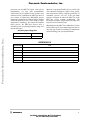
Freescale Semiconductor, Inc.
Semiconductor Products Sector
PowerPC™ G4 Architecture White Paper
Delivering Performance Enhancement in 60x Bus Mode
Freescale Semiconductor, Inc...
Susan Seale
You know the scenario: you’ve just released the
greatest whiz-bang product to the networking
marketplace—fantastic
features,
excellent
performance, and the right price. But right away,
you have to watch out for competitors approaching
from all sides. To maintain your leadership
position in the market, your mission—should you
choose to accept it—is to upgrade your product’s
performance (and of course lower its cost) with
minimal hardware and software redesign. Where
do you begin?
If your system is PowerPC-based, using the
MPC750 (G3) in particular, there are a variety of
options to consider. Some devices offer new
features. This makes the marketers happy. Most
new offerings deliver higher core frequency. Now
the software developers are happy. And many
PowerPC upgrades are drop-in replacements
because they have the same footprint as the device
you’re using today. Even the hardware team can
celebrate. Naturally, the right choice depends on
how in your current implementation your software
pushes the processor to its limits.
At this point in the analysis, most embedded
developers admit to one common bottleneck in the
processor subsystem: I/O bandwidth. No matter
how high you crank up the processor speed, how
big the on-chip caches are, or how fast the core can
execute an instruction, the limitation of your
system’s performance is dependent upon how
much data the processor can move in and out (with
significant manipulation in between).
Performance Enhancement
This paper highlights ways that the PowerPC
MPC74xx (G4) series can improve the I/O
bandwidth of your G3 system with minimal
engineering effort and can help you overcome the
barrier to best-in-class system performance.
Even without discussing the benefits of the
AltiVec™ processing unit available in G4
processors (let’s leave that exercise for an analysis
of SIMD-intensive applications.) or enhancements
offered by G4’s MPX bus mode option, there are
many reasons for choosing a G4-series processor
for your system. For now, let’s consider only those
benefits which apply to PowerPC systems using
the conventional PowerPC instruction set and the
standard 60x bus mode.
May we introduce the MPC7400/7410 and the
MPC7440/7450 devices.
Benefit 1. Higher Sustainable System
Bus Bandwidth
‘Peak bandwidth,’ the maximum number of bytes
that can be transferred in a single cycle, is a purely
theoretical number. By contrast, ‘maximum
bandwidth,’ the maximum number of bytes that
can be transferred over several transactions,
provides a value which takes into account the
memory system latency and the limitations
associated with the bus protocol, in this case the
60x bus. For example, the 60x bus requires one
dead cycle between address tenures and one dead
cycle between data tenures. In a real system, I/O
bandwidth is further limited by particular device
implementation constraints. (Refer to Benefit 2
below for more detail on one of the architectural
constraints of the MPC750—the inability to
pipeline cache loads.) ‘Sustainable bandwidth’
means the maximum number of bytes that can be
transferred over an extended number of cycles,
taking into account all of the constraints mentioned
above.
© Motorola, Inc., 2001. All rights reserved.
For More Information On This Product,
Go to: www.freescale.com
Freescale Semiconductor, Inc.
Performing a sequence of cacheable data loads over
a 100MHz bus, both the MPC750 and the
MPC74xx variants have a peak bandwidth of
800Mbytes per second. With the constraints of the
60x bus protocol and the same memory system
latency, both have a maximum bandwidth of
640Mbytes per second. However, in terms of
sustained bandwidth, which best represents actual
system performance, the MPC74xx devices
outperform the MPC750 by nearly 3:1.
Freescale Semiconductor, Inc...
Comparison of MPC750 and MPC74xx Bus
Bandwidth (Mbytes/sec.)1 at 100MHz
1
2
3
4
5
Device
Peak2
Maximum3
MPC750
800
640
2464
MPC74xx
800
640
6405
Sustained
Values assume a memory read latency of 10 bus cycles,
counted from the cycle when address is driven and TS is
asserted:
1. Processor bus to system logic
2. System logic to memory interface
3. SDRAM Activate command (assert RAS)
4. Wait for memory (activate to Read/Write = 2 cycles)
5. Read command (assert CAS)
6. Wait for memory (SDRAM Read Latency = 3 cycles)
7. Wait for memory (continued)
8. First beat on memory bus
9. Data latched into system logic (not necessarily required)
10. First beat on processor bus
Peak bandwidth (MPC750 and MPC74xx) = 8 Bytes/cycle
x 100MHz = 800 MB/sec.
Maximum bandwidth (MPC750 and MPC74xx) =
[(1 cache line)/5 bus cycles] x
100MHz = 32 Bytes x 100MHz/ 5 cyc = 640 MB/sec.
Sustained bandwidth (MPC750) = [(1 cache line)/13 bus
cycles] x 100MHz = 32 Bytes x 100MHz / 13 cyc = 246
MB/sec.
Sustained bandwidth (MPC74xx) = maximum bandwidth
(MPC74xx). By pipelining transactions on the address
bus, the MPC74xx does not incur any additional penalty
beyond the limitations of the 60x bus protocol.
Benefit 2. More Back-to-Back
Transactions on the Bus
Instructions
In the G3 architecture, once an I-cache miss occurs,
no further I-cache misses are issued to the L2 or the
system bus until the cache line fill updates both the
L1 and L2 caches. Thanks to an additional entry in
the
instruction
reload
table,
the
MPC7400/MPC7410 architecture allows a second
instruction fetch to start after the first fetch has
updated the L1, but before it has updated the L2.
Going a step further in improving instruction fetch
performance, the MPC7440/MPC7450 can support
up to two outstanding instruction fetches, compared
to just one for the MPC750 and the
MPC7400/MPC7410.
Data
As a result of the G3’s D-cache design, once a
D-cache miss occurs, no further D-cache misses
(triggered by program loads and stores) are
propagated to the L2 or the system bus until the
original missed data is returned. This means that
back-to-back cacheable data reads are not pipelined
on the bus. Even though the bus interface unit may
be ready for more transactions, and the 60x bus
protocol can accept another pipelined address
phase, the blocking caches add latency to a
sequence of read accesses. In order to prevent one
miss from blocking the cache for subsequent
accesses, the MPC7400/MPC7410 D-cache
supports ‘miss-under-miss.’ If a miss is pending,
subsequent loads that miss in the D-cache will
propagate to the bus, rather than stalling. In fact, the
load/store unit of the MPC7400/MPC7410 can
continue to issue requests until up to six misses are
pending. The MPC7440/MPC7450 can support up
to 16 outstanding data tenures on the bus, five of
which may be data load misses. (The others may be
stores, castouts, snoop pushes, or instruction
fetches.)
Better pipelining of instruction fetches and support
for multiple outstanding data transactions add up to
better bus utilization and higher sustainable
bandwidth than the MPC750 can provide.
Benefit 3. L1 Cache Access
Improvements
Load Miss Folding
In the MPC750, if there are two load misses to the
same cache block, the second load must wait until
the entire block is returned before it can access its
data. Subsequent accesses to the cache are also
stalled. When two load misses to the same cache
block occur in the MPC74xx, the stall does not
occur. Instead, as data beats return for the first miss,
results can be provided for the next miss as well.
Furthermore, up to four subsequent misses to the
same cache block can be ‘folded’ into a Load Fold
Queue, allowing full access to the D-cache for the
following instructions while the reload is in
progress. Non-blocked access to the cache,
combined with pipelining of back-to-back data
reads on the bus, can improve the performance of a
PowerPC system limited by bus bandwidth.
2
For More Information On This Product,
Go to: www.freescale.com
Freescale Semiconductor, Inc.
Store Miss Merging
If the MPC750 has two store misses to the same
cache block, the second store must wait until the
entire cache block is loaded before it can write its
data. By contrast, the MPC74xx merges several
stores to the same cache block. If enough stores
merge to write all 32 bytes of the cache line, then no
data needs to be loaded from the bus, and an
address-only transaction is broadcast instead.
Freescale Semiconductor, Inc...
Allocate on Reload
The MPC750 has a cache line replacement policy of
‘allocate on miss.’ When a miss occurs, the
MPC750 immediately identifies a victim block to
be castout. If a subsequent transaction needs to
access this victim block, the block will already have
been marked invalid and the transaction must reload
the recently castout data from the bus. This
thrashing generates unnecessary traffic on the bus.
The MPC74xx, however, does not identify the
victim block until after the requested block fill
occurs. This cache line replacement policy of
‘allocate on reload’ applies to both the L1 and L2
caches. If a subsequent transaction to another block
in the same set occurs during the reload, the access
hits (because no block in the set has been identified
as the victim block yet), and no additional bus
access is necessary. When the goal is maximum I/O
bandwidth, keeping accesses off the bus is just as
important as reducing the latency of transactions on
the bus.
Benefit 5. Private Storage to Off-Load
Traffic from System Bus
One enhancement introduced in the MPC755 and
featured in some G4 implementations is the option
to use a portion (or all) of the backside cache space
as private memory storage. The MPC750 does not
support this feature. When the private memory
storage feature is enabled in the L2 of a MPC7410
system or the L3 of a MPC7450 system, the
external cache memory can be partitioned, such that
some of the memory operates normally as cache
while some of the memory functions as a
direct-mapped address space. The direct-mapped
memory space is often used for storage of critical
sections of code (such as interrupt routines) or for a
data set requiring repeated manipulation. In either
case, accesses to this range of addresses do not
consume valuable bandwidth on the system bus.
Benefit 6. System Bus Improvements
While the MPC750 supports a maximum of
100MHz on the system bus, the MPC74xx supports
up to 133MHz. Using the same assumptions
described in Benefit 1, we can derive the bus
bandwidth for the MPC74xx processors with a
133MHz bus and add this data to the comparison:
Comparison of Bus Bandwidths in (Mbytes/sec.)
Device and Bus Frequency
Peak
Maximum
Sustained
MPC750
100MHz
800
640
246
Benefit 4. Larger Backside Cache with
Better Throughput and
Improved Reliability
MPC74xx
100MHz
800
640
640
MPC74xx
133MHz
1064
851
851
The MPC750 has access to only 1MB of backside
L2 cache, while the MPC7400/MPC7410 supports
up to 2MB of backside L2 cache (optionally
configurable as direct-mapped memory space—see
Benefit 5). The MPC7450 supports 256kB of
on-chip L2 as well as up to 2MB of backside L3.
These additional cache resources maximize the hit
rate and minimize the use of the long-latency
system bus.
Note that an upgrade from the MPC750 at 100MHz
to a MPC74xx at 133MHz can produce a sustained
system bus bandwidth improvement of more than
3x.
Another system bus improvement added to the
MPC7440/MPC7450 is support for a larger address
space via a new 36-bit extended addressing mode,
in addition to support for the 32-bit addressing
mode of the MPC750 and MPC7400/MPC7410.
For superior cache performance and reliability, the
MPC7450 adds DDR SRAM support and address
parity on the L3 bus. The MPC750 interfaces only
to synchronous burst SRAMs or late-write SRAMs
on the L2 bus and does not support L2 address
parity.
3
For More Information On This Product,
Go to: www.freescale.com
Freescale Semiconductor, Inc.
Benefit 7. Dual-Ported L1 Data Cache
Tags
Freescale Semiconductor, Inc...
In a dual-PowerPC architecture or a system with
one PowerPC processor and an additional system
bus master, bus snooping is required to maintain
coherency of data throughout the system. In the
MPC750, if a snoop is blocked because the data tag
is being accessed, the MPC750 must assert ARTRY,
notifying the current bus master to abort the
transaction and retry it later. The G4 architecture
eliminates this inefficiency by implementing
dual-ported L1 data tags. In the MPC74xx devices,
the bus snoop can proceed without being blocked
by a simultaneous access to the tags.
Benefit 8. Shared Cache State for Data
The MPC750 has an MEI cache coherency
mechanism, including Modified (M), Exclusive (E),
and Invalid (I) states for entries in the data cache.
Consider a dual-processor design using G3 devices
which we’ll identify as A and B. When A’s read
transaction generates a cache line fill, the incoming
block is allocated as Exclusive in A’s cache. If B
snooped A’s read transaction and detected a
Modified copy of the same block in cache, B would
have responded by pushing the cache block to
memory (and marking the line Invalid) so that A
would access the latest data during its cache line fill.
The next time B needs that data, however, B has to
read the line from memory. Even worse, if A has
modified the data in its cache by the time B is ready
to read it, the very same snoop sequence would be
repeated in reverse. That is, B would have to wait
for A to push the data to memory before retrieving
it. Each of these cache block pushes consumes
much-needed data bus bandwidth.
The MPC7400/7410 and MPC7440/MPC7450
have a 4-state cache coherency mechanism known
as MESI. The additional cache state is Shared (S),
and it is associated with a new 60x bus signal called
SHD. The new Shared state gives both processors in
a dual-processor system the capability to maintain a
valid copy of the same cache line simultaneously. In
the case of a read transaction by A and a snoop by
B, processor B would respond with an assertion of
SHD to notify A that this block has already been
cached elsewhere in the system. Processor A would
then load the incoming block into its own cache as
Shared, and B would change its cache block’s state
from Exclusive to Shared. Now both processors can
access the shared data without the need for a retry
transaction or snoop push. By limiting bus accesses,
the Shared capability significantly improves
performance in a symmetric multi-processing
system.
Benefit 9. Easy Upgrade from MPC750
The MPC7410 (Rev 1.4) has the same 3.3V I/O
supply voltage as the MPC750 on the system bus.
This consistency enables the MPC7410 to replace
the MPC750 while providing electrical
compatibility with existing logic on the PowerPC
system bus. Burst SRAMs are readily available at
the lower I/O voltage of the MPC7410’s L2 bus.
The MPC7400/MPC7410 also has the same
footprint as the MPC750. One new signal, L2VSEL
(previously a No-Connect on the MPC750), is used
in a MPC7410-based system to select the desired
L2 bus voltage of 2.5V or 1.8V. Another
No-Connect signal on the MPC750 is used as
BVSEL to select the desired system bus voltage
(3.3V, 2.5V, or 1.8V) for the MPC7410. The
MPC7400/MPC7410’s SHD pin (described in
Benefit 8) is also implemented on one of the
MPC750’s No-Connect pins. With just a few
hardware modifications, the MPC7400/MPC7410
is an easy drop-in replacement for the MPC750.
[For details on the signal differences between the
MPC750, MPC7400/7410, and MPC7440/7450
implementations, please refer to the “PowerPC 60x
Bus Implementation Differences Application
Note.” See “References” below.]
The core voltage is lower in the MPC74xx devices
than in the MPC750; however, this reduction,
combined with the smaller submicron geometry,
enables G4 devices to achieve higher operating
frequencies and improved I/O performance, while
minimizing the increase in power consumption.
For a uni-processor architecture, there is no need to
implement G4’s optional bus signals, which could
be used in MPX bus mode to support SMP (for
features such as intervention and snarfing).
And finally, G3 and G4 devices share a common
debug architecture, so the same extensive tools
support is available for MPC750 and MPC74xx
processors.
Benefit 10. G4 is from Motorola
Motorola’s commitment to the scaleability of the
PowerPC architecture is reinforced with each
high-performance product we add to the family.
The MPC74xx devices are no exceptions. G4
4
For More Information On This Product,
Go to: www.freescale.com
Freescale Semiconductor, Inc.
processors can run MPC750 object code with no
modifications; yet, they offer programmable
features that can be enabled for the system’s next
software release. In addition, the MPC74xx devices
are evidence of Motorola’s HiPerMOS process
technology advancements. With the help of smaller
submicron geometries, lower core voltages, copper
interconnect technology, and silicon-on-insulator
(SOI) process, the MPC74xx devices offer a
sizeable increase in operating frequency range over
their predecessors.
Freescale Semiconductor, Inc...
G4 Family Speed Upgrades
MPC7410
400 – 600MHz
MPC7440/MPC7450
600 – 800MHz
Motorola’s upcoming BookE devices, which will
offer enhanced integration, higher clock speeds,
and architectural features targeted specifically at
embedded systems, will run 32-bit user-mode
software developed for either the MPC750 or the
MPC74xx device without modification. The
investment you make in application code today will
be preserved in G4 and beyond.
Migrating from the MPC750 to Motorola’s G4 may
be one small step for your engineering team, but it’s
one large step toward overcoming I/O bottlenecks
and maximizing your system performance.
REFERENCES
Document ID
Title
AN2097
PowerPC 60x Bus Implementation Differences Application Note
AN1812
Common Footprint for MPC750, MPC755, MPC7400, and MPC7410
—
Migration Guide for Motorola MPC750, MPC755, MPC7400, MPC7410 PowerPC Processors
MPC7400UM
MPC7400 RISC Microprocessor User’s Manual
MPC7400EC
MPC7400 RISC Microprocessor Hardware Specifications
MPC7410EC
MPC7410 RISC Microprocessor Hardware Specifications
5
For More Information On This Product,
Go to: www.freescale.com
Freescale Semiconductor, Inc...
Freescale Semiconductor, Inc.
DigitalDNA and AltiVec are trademarks of Motorola, Inc.
The PowerPC name, the PowerPC logotype, and PowerPC 603e are trademarks of International Business Machines Corporation used by Motorola
under license from International Business Machines Corporation.
Information in this document is provided solely to enable system and software implementers to use PowerPC microprocessors. There are no express
or implied copyright licenses granted hereunder to design or fabricate PowerPC integrated circuits or integrated circuits based on the information in
this document.
Motorola reserves the right to make changes without further notice to any products herein. Motorola makes no warranty, representation or guarantee
regarding the suitability of its products for any particular purpose, nor does Motorola assume any liability arising out of the application or use of any
product or circuit, and specifically disclaims any and all liability, including without limitation consequential or incidental damages. “Typical” parameters
which may be provided in Motorola data sheets and/or specifications can and do vary in different applications and actual performance may vary over
time. All operating parameters, including “Typicals” must be validated for each customer application by customer’s technical experts. Motorola does
not convey any license under its patent rights nor the rights of others. Motorola products are not designed, intended, or authorized for use as
components in systems intended for surgical implant into the body, or other applications intended to support or sustain life, or for any other application
in which the failure of the Motorola product could create a situation where personal injury or death may occur. Should Buyer purchase or use Motorola
products for any such unintended or unauthorized application, Buyer shall indemnify and hold Motorola and its officers, employees, subsidiaries,
affiliates, and distributors harmless against all claims, costs, damages, and expenses, and reasonable attorney fees arising out of, directly or indirectly,
any claim of personal injury or death associated with such unintended or unauthorized use, even if such claim alleges that Motorola was negligent
regarding the design or manufacture of the part. Motorola and
are registered trademarks of Motorola, Inc. Motorola, Inc. is an Equal
Opportunity/Affirmative Action Employer.
World Wide Web Addresses: http://www.motorola.com/PowerPC
For More Information On This Product,
Go to: www.freescale.com

![PC755BM8 [Preliminary]](http://vs1.manualzilla.com/store/data/005786860_1-ac3ee01c2b00aeb18fc7f0a57a841c91-150x150.png)