1
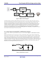
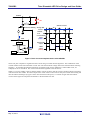
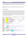
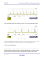
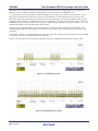
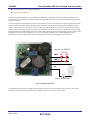
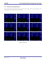
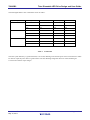
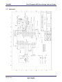
APPLICATION NOTE 78K0/IB2 Triac Dimmable LED Drive Design and User Guide R01AN0520EU0100 Rev.1.00 May 13, 2011 Introduction This application note provides a guide to designing Triac dimmable High Brightness LED drives with Renesas Electronics’ 8-bit 78K0/IB2 microcontrollers (MCUs). This document includes: • Overview of LED drives • Overview of Triac dimmers • Triac dimmable LED drive solution example • Reference design example with Renesas 78K0/IB2 microcontroller LED lighting is one of the most promising solutions to deal with the increasing energy demands as natural resources around the world are becoming more expensive and less viable to sustain the needs of ever increasing populations around the world. The awareness of the impact energy production has on the environment as well as the continuous strive of human kind to make things better and more efficient caused an unprecedented concentration of R&D efforts and capital investments in the development of the LED lighting industry. Compared with the traditional incandescent light bulbs LED light engines are up to 80% more efficient in terms of light output and 10 times longer lasting. Compared with other energy efficient lighting solutions such the compact fluorescent lights (CFL) or high-intensity discharge (HID) lamps which contain harmful substances like mercury, LED lights are less of a threat to the environment and offer far better color management and dimming capabilities. Although the LED is a very simple low voltage low current device, to make it compete with its predecessors it needs a fair amount of other LEDs working together under the control of relatively complex electronics circuits. The key to getting the maximum light output of and LED is to drive it with a constant current that is right at or bellow the rated spec. Providing this constant current can be accomplished by simply using a series resistor but this is not what an energy efficient solution should look like. Instead a full on/off current chopping method with a resulting average current through the LED is used to get maximize efficiency while making sure that the LED works in a save operating region. Target Devices 78K0/Ix2 Family R01AN0520EU0100 Rev.1.00 May 13, 2011 Page 1 of 28 78K0/IB2 Triac Dimmable LED Drive Design and User Guide Contents 1. Overview ........................................................................................................................................... 3 1.1 LED Drives ........................................................................................................................................ 3 1.2 Triac Dimmers ................................................................................................................................... 3 2. Microcontroller Based Triac Dimmable LED Drive............................................................................ 4 2.2 Power Factor Correction (PFC) - DC/DC Boost converter ............................................................... 5 2.3 DC/DC Buck Converter - Constant Current LED Drive..................................................................... 7 3. Design Example ................................................................................................................................ 9 3.1 Design Data....................................................................................................................................... 9 3.2 Buck Converter Target PWM Duty, Ton and Toff ............................................................................. 9 3.3 Inductor Voltage, VLon and VLoff ..................................................................................................... 9 3.4 Inductor Calculation ........................................................................................................................ 10 3.5 4. 4.1 4.2 4.3 Ton, Toff Adjustment....................................................................................................................... 10 Design Guidelines ........................................................................................................................... 11 Changing Number of LEDs ............................................................................................................. 12 Changing LED Current.................................................................................................................... 12 Adjusting Buck Converter Ton, Toff ................................................................................................ 12 5. Triac Controlled Dimming................................................................................................................ 13 6. Benefits to Using 78K0/Ix2 for Triac Controlled Dimming............................................................... 15 7. 7.1 7.2 7.3 7.4 7.5 Triac Dimmable LED Drive Reference Design................................................................................ 16 Operation......................................................................................................................................... 17 Demo............................................................................................................................................... 19 Over-current Protection................................................................................................................... 20 Performance Evaluation Data ......................................................................................................... 22 Schematic........................................................................................................................................ 24 8. References ...................................................................................................................................... 27 8.1 LED Driver References ................................................................................................................... 27 Revision Record ...................................................................................................................................... 29 General Precautions in the Handling of MPU/MCU Products................................................................. 30 R01AN0520EU0100 Rev.1.00 May 13, 2011 Page 2 of 28 78K0/IB2 Triac Dimmable LED Drive Design and User Guide 1. Overview 1.1 LED Drives Ordinary LEDs used in signaling applications are simple low voltage low current device that do not have enough light output to compete with incandescent or fluorescent light sources. A special line of high brightness LEDs can run at much higher currents and with the aid of special lenses and phosphor coatings can deliver quality light that is brighter and more uniform than previously mentioned sources. Compared with 10-20mA forward currents of signaling LEDs, high-brightness LEDs can be driven with hundreds of milliamps. To drive these LEDs efficiently special circuits needed to be developed. The key to getting the maximum light output of and LED and maintain the same color temperature is to drive it with a very high constant current and manage to dissipate the excessive heat developed during the process. A typical constant current drive uses a on/off current chopping circuit to ensure an average current through the LED that is in the safe operating range. 1.2 Triac Dimmers In the following paragraphs we will explain the basics of the Triac dimming and the challenges they pose to LED dimming drives. Figure 1 shows a typical commercially available Triac dimmer circuit used to dim incandescent light bulbs. VR Triac 120VAC ∼ Diac R Incandescent light bulb C Figure 1 Triac Dimmer By adjusting variable resistor VR, capacitor C charges up with a delay set by the total RC constant. Regardless of polarity when the voltage on the capacitor reaches a certain threshold, the Diac starts to conduct and it triggers the conduction of the Triac. An illustration of the conduction angle is shown in Figure 2. The Triac starts conducting after a delay set by the RC circuit and stays on until the first half cycle completes and AC voltage reaches zero. On the following cycle the capacitor will charge up with the opposite polarity voltage and the Triac will turn on again after the delay set by the RC constant. By adjusting VR we can effectively vary the Triac conduction or phase angle and the resulting average AC voltage across the light bulb. R01AN0520EU0100 Rev.1.00 May 13, 2011 Page 3 of 28 78K0/IB2 Triac Dimmable LED Drive Design and User Guide Phase Phase Figure 2 Triac Conduction Triac dimmers, also called wall dimmers, are widely used in residential and commercial buildings with incandescent light bulbs but they present serious limitations and challenges when used with alternative lighting solutions such as CFLs or LEDs. The biggest problem LED drive designers face is the fact that the load has to draw minimum current to maintain the Triac in conduction. LED light engines draw a fraction of the power incandescent light bulbs draw, causing the Triac to shut off during the conduction cycle resulting in visible light flicker. To maintain a minimum current through the Triac, often additional resistive loads are used, but of course this increases power consumption and lower’s the overall efficiency the LED lights are meant for. Another problem Triacs have is the susceptibility to the switching noise the drive introduces causing shut off and flicker on the output. Effective ways to deal with this is to provide adequate filtering. As it will be seen in the following chapter, LED drives are electronic circuits containing power switches and inductors seen from the AC mains side as nonlinear loads with poor power factor. One of the basic requirements utility companies mandate for LED drives is to have power factor correction (PFC) circuits. This application note shows how the Renesas K0/Ix2 dedicated lighting microcontroller can be effectively used to implement both the Triac dimmable LED drive and an active power factor correction function. 2. Microcontroller Based Triac Dimmable LED Drive The basic requirement for a dimmable drive is to be able to track the Triac slider position which corresponds to the effective conduction angle and use this information to dim the light output on a chain of LEDs. The useful range for the phase angle of a commercial Triac dimmer is between 45 to 135 degrees. A block diagram of the drive is shown in Figure 3. R01AN0520EU0100 Rev.1.00 May 13, 2011 Page 4 of 28 78K0/IB2 Triac Dimmable LED Drive Design and User Guide Figure 3 LED Drive Block Diagram The bridge rectifier provides the 120 Hz unfiltered output to the PFC circuit and to a DC power supply circuit not shown in this block diagram. The PFC block provides power factor correction and boosts the voltage to 200V DC to 400V DC to be used by the Buck converter stage. The Buck converter converts the DC voltage to a lower value depending on the number of LEDs it is driving. A conduction angle detect block is used for dimming reference. The controller is the Renesas 78K0/Ix2 8-bit dedicated lighting microcontrollers. The right mix of peripherals and CPU performance make the 78K0/Ix2 an ideal device for lighting applications. Three on-board hardware comparators supporting two 16-bit PWM timers can drive external MOSFET switches for both the PFC circuit and the Buck converter with minimum CPU support. The timers have Hi-impedance states controlled by the comparators so that at a fault condition the external power circuits are protected. 2.2 Power Factor Correction (PFC) - DC/DC Boost converter The PFC circuit is based on a typical DC/DC boost power converter shown in Figure 4 DC/DC Boost Converter bellow. The role of the DC/DC boost converter stage is to boost a rectified input voltage to 200V- 400V DC needed for the DC/DC buck converter stage. In order to do that, a switching device such as a MOSFET is driven by typically a PWM signal. When the switching transistor is on the current flows and builds up through the inductor to the ground storing energy in the inductor. When the transistor is off, the energy stored in the inductor generates a voltage with positive polarity at the anode the diode. The voltage seen on the anode of diode D is the sum of inductor voltage and VDCIn and it charges up capacitor C to a higher voltage than the input VDCIn, making it a boost DC/DC converter. The voltage on the output can be precisely controlled by the duty cycle of the PWM signal. By monitoring the output voltage, the PWM duty cycle can be adjusted to maintain a certain value. VDCIn L PWM D T VDCOut C Z Figure 4 DC/DC Boost Converter R01AN0520EU0100 Rev.1.00 May 13, 2011 Page 5 of 28 78K0/IB2 Triac Dimmable LED Drive Design and User Guide If the load is nonlinear or inductive, the current seen at the AC input side will lag behind the voltage and it may also be distorted with large peaks causing a power factor of less than 1. Close to unity power factor is desirable to reduce harmonic distortions that can creep back into the line as well as to eliminate the excessive currents that lead to overheating of the supply lines which result in power losses. To achieve this, the DC/DC boost circuit switch can be controlled in such a way that the current stays in phase with the voltage and the distortions are eliminated. There are three common methods of controlling the current through the load based on the time the switch is held off after it was previously turned on to allow the current build up through the inductor. One method called the continuousconduction-mode (CCM) will turn the transistor off for a very short time so that the current never drops to 0. The second method is the critical-conduction-mode (CRM) in which the transistor is off until the entire energy stored in the inductor is discharged into the capacitor and the current decreases to 0 at which time the transistor is turned on again and the cycle repeats. The third method called the discontinuous-conduction-mode lets the current through the inductor decrease until it reaches 0 but the transistor is not turned on right away, only after some delay. The PFC circuit in this application note uses critical-conduction-mode active power factor correction and achieves a power factor of better than 95%. Critical-conduction-mode (CRM) uses a constant ON-time pulse to charge the inductor, then allows the current to fully discharge before initiating the next constant ON time pulse. One of the advantages of this method is that it eliminates reverse recovery losses in the boost diode and allows the use of a smaller, lower cost diode. Typical applications for this method are low power converters where losses are critical to the efficiency bottom line. The implementation with the 78K0/IB2 microcontroller is shown in Figure 5 bellow. The OFF-time for the switching PWM signal can be precisely controlled by one of the built-in comparators. The algorithm uses only one 16-Bit timer and one comparator to implement the power factor correction, in this case timer TX0 and comparator 2. The only CPU intervention required is to adjust the ON-time of TMX0 to maintain the constant DC boost voltage on the output. The ON-time is adjusted in software based on the feedback provided by the 10-bit ADC, as described bellow. DC BUS 85 – 265 VAC Rectified, unfiltered Average AC Critical Conduction Mode (CRM) T Zero current detection TMX00 ANI0 78K0/IB2 TMX0 A/D TMX00 (PFC output) Interlock TX0CR0 (PFC-on pulse width) CMP2+ Internal Triac angle decoder TI00 TX0CR1 (PFC-off pulse TM00 CMP2+ (Zero current detection) Figure 5 PFC Implementation with 78K0/IB2 R01AN0520EU0100 Rev.1.00 May 13, 2011 Page 6 of 28 78K0/IB2 Triac Dimmable LED Drive Design and User Guide The CRM algorithm uses a constant ON time but to maintain a constant boost voltage on the output the ON time needs to be adjusted in a control loop. With the Triac varying the voltage on the input, Ton will be larger at low levels and shorter at the higher levels. The load presented by the LED Buck driver will also lead to variations in the ON-time. The initial ON-time is selected for 120V nominal input voltage. About every 2ms, the PFC boosted voltage is measured and the on-time is adjusted up or down. The aux winding of the PFC inductor detects when current falls to zero using comparator 2. When zero current is detected by the voltage going below 0.3V for 100ns, timer TX0 is restarted turning on the PFC switch for the on time pulse. As a safeguard, a 0.05 ohm sense resistor is used in the ground return path to the bridge rectifier. The sensed voltage is amplified by the on board Op Amp and the output of the Op Amp is used to trigger comparator 1 which is configured to set timer TX0 and TX1 outputs to Hi-Z. External circuitry makes certain the PFC and Buck switches are off when the microcontroller outputs are Hi-Z. Another key element for success is the size of the capacitor between the bridge rectifier and the PFC circuit. When the Triac switches on at 50% dimming level, a voltage spike of 170V (at 120VAC) is presented to the bridge rectifier circuit from the Triac output. To maintain power factor across dimming, it is important to keep this capacitor size as small as possible balancing noise levels with inrush current. One indication that the capacitor is too large will be excessive heat in the bridge rectifier and inrush limiting resistor in the power supply. 2.3 DC/DC Buck Converter - Constant Current LED Drive VDCIn C D LEDs L PWM T Current sensing R By Comparator 0 Figure 6 DC/DC Buck Converter The buck constant current LED driver uses comparator 0 and a sensing resistor R to set a typical current through a chain of LEDs on the output. The resistor value is chosen so that the voltage drop generated by the average current is within the 0.05V to 1.6V threshold range of the comparator. For 1 ohm resistor value for example and a typical 350mA LED current this would be 0.35V. To support higher or lower LED current with a given R we just need to change the comparator threshold voltage. Resistor R should be as small as possible to reduce the losses. The implementation of the DC buck converter with the K0/IB2 is shown in Figure 7 below. R01AN0520EU0100 Rev.1.00 May 13, 2011 Page 7 of 28 78K0/IB2 Triac Dimmable LED Drive Design and User Guide DC BUS LED L T Inductor current LED Current Sensing Average LED current Internal Vref Current Sense Input (CMP0+) TMX1 Internal CMP output TMX1 Dimming Interlock CMP0 TMH1 PWM output (TMX10) Ton Toff Internal Vref Figure 7 Buck Converter Implementation with 78K0/IB2 Timer TX1 plus comparator 0 regulate the buck current using a constant off time algorithm. The combination of the constant off time Toff and a maximum on time Ton limit the maximum voltage and set the maximum buck switching frequency. To calculate the minimum off time an acceptable ripple current (100ma for a 350ma LED circuit, for example) has to be considered. The constant off time buck algorithm works as follows: When T is on, timer TMX1 counts up and the inductor current increases until the sensing comparator detects maximum value and resets timer TMX1. The timer output and T will be off for a time interval set by the constant Toff. During this time the inductor discharges by ripple current value and when Toff expires, T is turned on again until the inductor current reaches again the comparator threshold or a the maximum time Ton. R01AN0520EU0100 Rev.1.00 May 13, 2011 Page 8 of 28 78K0/IB2 Triac Dimmable LED Drive Design and User Guide 3. Design Example In this chapter we will show a practical example on how to calculate Toff and maximum Ton . The number of LEDs we chose to drive for this example will be 7 at a constant current of 350 mA and a typical forward voltage drop of 3.5V. The buck input voltage is 200V and the inductor value is 1mH. The acceptable ripple current will be 100mA. 3.1 Design Data Vboost: 200 V -buck input DC voltage Rds(on): 1.2 ohm -MOSFET drain-source on resistance Iled: 0.35 A -LED constant current Iripple: 0.1 A -acceptable LED ripple current Vf(LED) : 3.5 V -LED forward voltage at rated current #of LEDs: 7 -number of series connected LEDs Vf(LED chain): 24.5 -forward voltage of LED chain Vd: 1V -forward voltage of flyback diode Rsense: 2.4 ohm -current sensing resistor F: 100000 Hz -target frequency 3.2 Buck Converter Target PWM Duty, Ton and Toff Duty = Ton = Vf + Vd 24.5 + 1 = = 12.83% Vboost − Rds ∗ Iled − Rsense ∗ Iled 200 − 1.2 ∗ 0.35 − 2.4 ∗ 0.35 1 0.01283 = = 1283ns F ∗ Duty 100000 Ton _ cycles = Ton / 25 = 51 cycles Toff = 1 − Ton = 10000ns − 1283ns = 8717us F Toff _ cycles = Toff / 25 = 349 cycles 3.3 Inductor Voltage, VLon and VLoff VLon = Vboost − Rds * Iled − Rsense * Iled = 200 − 1.2 * 0.35 − 2.4 * 0.35 = 174V VLoff = Vf + Vd = 24.5 + 1 = 25.5V R01AN0520EU0100 Rev.1.00 May 13, 2011 Page 9 of 28 78K0/IB2 Triac Dimmable LED Drive Design and User Guide 3.4 Inductor Calculation Lon = VLon ∗ Ton 174 ∗ 1283 ∗ 10 −9 = = 2235uH . Iripple 0 .1 Loff = VLoff ∗ Toff 25.5 ∗ 8717 ∗ 10 −9 = = 2223uH . Iripple 0 .1 Minimum inductor value is chosen to be the maximum of the two + 10%: L min = 2235 ∗ 1.1 = 2458uH . 3.5 Ton, Toff Adjustment Will select a standard 2.2 mH inductor which will give us slightly higher frequency and will calculate Ton and Toff for the buck converter PWM drive signal based on Lmin = L-10% L = 2200uH . Ton = L min = L * 0.9 = 1980uH . L min∗ Iripple 1980 ∗ 0.1 ∗ 10 −6 = = 1138us. VLon 174 Ton = 1138 / 25 = 46 cycles Toff = L min∗ Iripple 1980 ∗ 0.1 ∗ 10 −6 = = 7765ns. VLoff 25.5 Toff = 7765 / 25 = 311 cycles Ton and Toff are expressed as multiples of in 25ns clock cycles and will be the values written to timer TMX1 compare registers. Ton and Toff limit the output voltage. The minimum output voltage of the buck converter is also limited by the delay in the current sense circuit and internal comparator delay filters. The total time delay will be Toff + delay in the current sense circuit. The typical current sense circuit delay is 300ns. With Toff value calculated in this design example the minimum time transistor T is on, we can calculate the minimum voltage at the output of the buck converter: Toff = 311 cycles = 25ns * 311 = 7765ns Ton minimum = 300ns (due to delay in current sense circuit) Duty = 300ns/(300ns + 7765ns) = 3.7% Vout = Vin * DUTY = 200V * 3.7% = 7.4V CAUTION: In this case this minimum voltage of 7.4 V is critical and limits the minimum number of LEDs we can drive. If the added forward voltages of the series connected LEDs is less than 7.4V without changing the Toff parameter, will cause damage to the device. The buck circuit will not be able to limit the current and will try to dump R01AN0520EU0100 Rev.1.00 May 13, 2011 Page 10 of 28 78K0/IB2 Triac Dimmable LED Drive Design and User Guide 7.4V into a chain of diodes with a lower maximum voltage. Since diodes have a very steep V/I curve, the I will increase exponentially leading to failure in the buck circuit. Calculate Toff parameter using the buck_calculator.xls spreadsheet for your diodes before plugging in the board to make sure the parameters are compatible with your LED array. The timer is programmed with the two intervals to happen in sequence: minimum off-time first, maximum ontime second. The maximum on-time will ordinarily be interrupted when the comparator resets the timer back to 0 restarting the minimum off time. The counter will not start counting until the comparator has dropped below the comparator threshold for >300ns. 4. Design Guidelines As previously shown the output voltage across the LED string is roughly the boost voltage times the buck converter frequency duty cycle. For a given boost voltage, number of LEDs, inductor value and ripple current we can calculate Toff and Ton which will correspond to the buck converter frequency and duty cycle to produce the desired output voltage. In this design we use a constant Toff method and limit Ton on cycle-by-cycle basis as the comparator detects the maximum allowed current through the LEDs. This cycle-by-cycle current limiting during Ton will result in a constant average current through the LEDs One of the basic requirements for this scheme to work is to have Ton set large enough to allow the comparator to trip before Ton expires. To help with the design we implemented a buck converter calculator tool in Excel called “buck_calculator.xls”. The calculator takes in the data shown in the design example and generates Ton and Toff in 25ns clock cycles for timer TX1. The excel calculator page shown in Figure 8 bellow can be provided along with the sample code. Figure 8 Buck Calculator R01AN0520EU0100 Rev.1.00 May 13, 2011 Page 11 of 28 78K0/IB2 Triac Dimmable LED Drive Design and User Guide 4.1 Changing Number of LEDs When changing the number of LEDs, PWM Ton and PWM Toff need to be recalculated and this can be easily done with the excel calculator “buck_calculator.xls” by simply plugging in the new number. The sample code developed to support this application note has two defined values BUCK_TOFF and BUCK_TON_MAX used as load values for timer TX1 compare registers to generate the PWM signal driving the buck switch Q1. BUCK_TOFF corresponds to Toff and PWM_TON_MAX corresponds to PWM Ton + PWM Toff. The minimum number of LEDs for the resulting PWM Toff will be limited by the minimum forward voltage drop as shown in the design example above. If we use the value of 7.76 us from the design example above, the minimum forward voltage will be 7.4V resulting in a minimum number of LEDs of 3. The maximum number of LEDs will be limited by the maximum power we can provide on the buck converter output The number of LEDs times the average LED current times the LED forward voltage drop cannot exceed this maximum output power. If for example the rated output power is 20W, the maximum number of LEDs will be limited to 16. 4.2 Changing LED Current LED forward current differs from manufacturer to manufacturer or part number to part number. The constant current regulation needs to match the LED forward current for the nominal output and should not exceed the value specified in the datasheet. To adjust the LED current we simply need to adjust Comparator 0 threshold that is used to detect the current on a sensing resistor. This threshold can be adjusted between 0.05V to 1.6V in 32 steps by changing the value of Comparator 0 configuration register C0RVM. To measure the LED current a common digital multi meter can be used. Adjust the LED current to not exceed the maximum value specified in the datasheet at the maximum AC input voltage. Maximum LED current + ripple current cannot exceed the buck inductor rated current and the rated output power. If the inductor rated current is 700 mA for a ripple current of 100mA than the maximum average LED current is 600mA. With 600mA LEDs considering a typical forward voltage of 3.5V per LED, the maximum number of LEDs we can drive at 600 mA is (20/0.6)/3.5 which is 9. To drive LEDs with higher currents that exceed the inductor current rating not only the inductor needs to be changed but it may also require a higher current recovery diode as well as a higher current boost inductor. 4.3 Adjusting Buck Converter Ton, Toff From the design example above Toff is 311 cycles and Ton is 46 cycles resulting in a switching frequency of 112.3KHz. If we consider 90% efficiency, these numbers will have to be increased by at least 10% to give us Toff = 342 and Ton = 51. The PWM dimming method described in the following chapter 5, uses timer TMH1 PWM output to gate buck timer TX1 output. As it can be seen in the waveforms in Figure 9 and Figure 10 below, Ton needs to be further increased to ensure proper inductor charge up after each dimming cycle. Figure 9 shows the waveform on the buck sensing resistor. After each dimming cycle the current through the inductor has to rise from 0 to 350 mA + Iripple/2 (50 mA). If Ton is too short, it takes multiple pulses to charge up the inductor. This will most likely produce flicker on the output when the dimming is at the lower range. R01AN0520EU0100 Rev.1.00 May 13, 2011 Page 12 of 28 78K0/IB2 Triac Dimmable LED Drive Design and User Guide Figure 9 Buck Ton too short Ton has to be adjusted so that the inductor can charge up in one pulse as seen in Figure 10 below. The first pulse is wider because we allow a larger Ton. The subsequent pulses are narrower as the comparator threshold is reached. Figure 10 Buck Ton adjusted Other practical consideration for choosing the right values for Ton and Toff is to allow the buck frequency to be as low as possible to improve efficiency and reduce the switch transistor and fly back diode heat dissipation. 5. Triac Controlled Dimming The Triac dimming level set by the dimming knob needs to be decoded and used as the reference input for the LED dimming. The 16-bit timer TM00 with a 78.125kHz clock measures the positive pulse width on the AC sense line at input pin TI000 on the microcontroller. To implement dimming based on the Triac’s coduction angle a unique timer interlocking feature of the K0/IB2 microcontroller is employed. The 8-Bit TMH1 timer is configured as a PWM timer and its output is used to gate the output of the Buck converter PWM timer TX1. The Triac conduction angle as R01AN0520EU0100 Rev.1.00 May 13, 2011 Page 13 of 28 78K0/IB2 Triac Dimmable LED Drive Design and User Guide measured by timer TM00 is translated into an 8-Bit number and loaded to timer TMH compare register CRC00. In effect the conduction angle controls the LED dimming in 256 steps through timer TMH duty cycle. To compensate for the Triac asymmetric conduction quadrants an average of more than two measurements is used. Pulses that are smaller than a minimum set value are rejected and are not used to adjust the running average. The algorithm compares the measured average with the current timer TMH duty cycle setting and adjusts the duty cycle to compensate. If the difference is significant the duty cycle is adjusted more quickly towards the new setting. When the TMH PWM setting is within 30 counts of the average, the PWM setting is adjusted by a smaller increment (+/- 1). This reduces flicker and provides a smooth ramp to the new level. At power-up, the TMH PWM duty is set to the minimum level. When the light is turned on at full brightness, timer TMH PWM duty ramps up to full brightness providing a soft start effect. At lower dimming levels, this effect is less noticeable. Timer TMH is used as a 1.2kHz PWM gating for timer TX1 output. The value derived from TI000 input of timer TMM is scaled to a value between 3 and 254 and (1.2% and 100%). Figures 11 and 12 bellow show the effect of dimming through timer TMH PWM method at 40% and near 100%. Figure 11 PWM Dimming at 40% Figure 12 PWM Dimming near 100% R01AN0520EU0100 Rev.1.00 May 13, 2011 Page 14 of 28 78K0/IB2 Triac Dimmable LED Drive Design and User Guide Using timer TMM measurement value of the Triac pulse width directly to set timer TMH duty cycle could result in flickering due to asymmetry in the Triac pulse width. Pulse rejection and cycle averaging are necessary for a stable, flicker free light output. 6. Benefits to Using 78K0/Ix2 for Triac Controlled Dimming As demonstrated throughout this application note, the 78K0/Ix2 dedicated lighting microcontroller can successfully address the basic requirements of Triac dimmable LED drives such as constant LED current control and power factor correction,but is it justified to use a microcontroller for this type of application? Most existing analog solutions achieve only 0.75 power factor which may be enough for residential lighting but not enough for industrial or commercial applications where the requirement is 0.9. The solution presented in this document uses active power factor correction to achieve better than 0.97. The constant current control implemented with the internal comparator has an adjustable threshold allowing great flexibility when changing the type or the number of LEDs and input voltage. The designer must also be aware, that not all Triacs are the same. Conduction angle varies across different models or manufacturers. Newer models advertise energy efficiency by simply limiting the conduction angle. Some dimmers will dim down and others will cut off the light all together at some point. The result is different voltage output and different dimming range. By using a microcontroller such as the Ix2 with a simple push of a button both the low level and high level dimming can be calibrated so that the same dimming range can be set for all different Triacs we use. In addition the Ix2 provides connectivity options through standard microcontroller interfaces such UART, SPI or IIC to allow the control of the LEDs from a remote location or as part of a network such as ZigBee or power line communication. The Ix2 supports the DALI protocol through its on-chip dedicated DALI communication interface and DMX12 can be easily implemented through the UART port. Dimming for example can be controlled from any of the listed network options through the same PWM method described in the application note but also from standard 0-10V DC devices through the ADC interface. The same ADC can be used to connect temperature or occupancy sensors that can report back to a network controller. In conclusion a Renesas 78K0/Ix2 based LED drive solution expands the possibilities far beyond just replacing the light bulb with a more efficient one. It can sense the environment, think for itself, and interact with other lights and systems to allow better and even more efficient management of energy resources. R01AN0520EU0100 Rev.1.00 May 13, 2011 Page 15 of 28 78K0/IB2 Triac Dimmable LED Drive Design and User Guide 7. Triac Dimmable LED Drive Reference Design The following chapters describe the reference design that was built based on the design guide we developed in the previous chapters. The board picture is shown in Figure 13 Triac Dimmer Reference Design and the schematic can be found at the end of this document. The board is a compact 2”x 2” (50.8 mm x 50.8 mm) 4-layer PCB populated on both sides. The code is programmed into the MCU and it only needs the input AC power, the triac and the LEDs connected. CAUTION: Users of this board must be aware that high voltage up to 450V DC is present and there is a high risk of electric shock if the board or any components are touched. The design topology is non-isolated meaning that the LED output is directly connected to the high-voltage DC bus. The low-voltage ground for the MCU and digital components, is common to the high-voltage ground and it is connected to the AC neutral (i.e. Power Line referenced). Do not touch any of the components on the board while the AC power is applied. PFC switch Debug port Buck inductor LED connector AC connector 78K0/IB2 Buck switch PFC Inductor Bulk capacitor Figure 13 Triac Dimmer Reference Design To download or to debug the code a custom 6-pin connector was used. To connect the MINICUBE2 we made a small interface PCB shown in Figure 14 below. Please note that the debug port is not isolated and connecting MINICUBE2 to the PC while the AC power to the board is applied, may result in damage to the PC and it also poses the risk of electric shock. Use a USB isolation hub such as the B&B UISOHUB4 when debugging or flash programming this board. R01AN0520EU0100 Rev.1.00 May 13, 2011 Page 16 of 28 78K0/IB2 Triac Dimmable LED Drive Design and User Guide Figure 14 MINICUBE2 interfaceing 7.1 Operation CAUTION Before connecting the board to the AC power line, please be aware that this is a non-isolated design. The user should not touch any part of this board to avoid the risk of electric shock. The board specifications are as follows: Input voltage: 85 to 265VAC Output power: 20W max. LED voltage range: 20 to 65VDC Constant LED current regulation z Buck converter: constant-off PWM with hardware comparator z LED current: 350mA z LED ripple current: +/-50mA Active Power Factor Control z Critical conduction mode using hardware comparator z Power factor: >0.95 @maximum power (20W) Dimming range: 1.5% to 100% Power efficiency: > 80% @ full brightness (20W) PFC boost voltage output stability: +/- 10% R01AN0520EU0100 Rev.1.00 May 13, 2011 Page 17 of 28 78K0/IB2 Triac Dimmable LED Drive Design and User Guide Over-current and over-voltage protections 2 x 2 inch, 4-layer PCB The LEDs used in this design were two modules of 9 LEDs each connected in series. With 350mA and around 3.2V forward voltage per LED the two modules make up for 20W load. The board has the code programmed and it is ready to operate once the As seen in Figure 15 the board has two sets of screw terminals, one for the incoming AC voltage and one for the LEDs. The board works with input voltages between 85VAC and 265VAC, but the firmaware has to be changed in order to operate at either 85VAC to 135VAC or 175VAC to 265VAC ranges. Make sure you have the correct version of the firmware before connecting the AC power. The triac dimmer to be used can be any retail wall dimmer, but please note that the dimming range and holding currents will differ and the results may differ. If the holding current is higher, when the dimmer is at lower position, flicker may occur. In our reference design we use a 10K/10W bleeder resistor connected across the AC input. This resistor is optional and the value varies depending on the triac used. Output: 20-65VDC, 350mA LEDLED+ L N Input: 85-265VAC Figure 15 Board connections To operate the board, connect the LEDs and the dimmer as shown in Figure 15 and apply the AC power. The LEDs should turn on and the intensity should follow the dimming level set by the triac control knob. R01AN0520EU0100 Rev.1.00 May 13, 2011 Page 18 of 28 78K0/IB2 7.2 Triac Dimmable LED Drive Design and User Guide Demo For demonstration purposes a few fully enclosed units were built. The demo shown in Figure 16 shows uses two 10W LED light modules to make up the full load of 20W. Each module consists of 9 LEDs connected in series. The LED maximum current was 350mA. To operate the demo, plug the power cord into the AC outlet and turn on the dimmer switch. The LEDs should come on and the light intensity should follow the dimmer slider setting. Load Switch Triac Dimmer LED Module LED Drive Figure 16 Demonstration unit At the low end of the dimming range when the load is very light, flicker may occur due to the fact that the load current may be lower than the triac holding current. To eliminate the flicker turn on the load switch located at the back side of the enclosure. This will connect a light load of 10 K across the dimmer output and line neutral. R01AN0520EU0100 Rev.1.00 May 13, 2011 Page 19 of 28 78K0/IB2 7.3 Triac Dimmable LED Drive Design and User Guide Over-current Protection The board is protected against over-currents through a 0.5 ohm sensing resistor Rs placed in the return path of the common ground. The negative voltage across the resistor is summed with an external reference voltage Vref and amplified by the internal OP Amp as seen in Figure 17 Over-current protectionThe output of the OP Amp is connected to the input of the internal comparator CMP1. DC BUS Rectified AC Input LED L T2 T1 Rs LED Current 0.5 Sensing Zero current Shunt Resistor detection TMX00 ANI0 TMX10 Hi-Z Control CMP2+ Vref A/D TMX1 Interlock 2.5V Vs TMX0 Interlock CMP0+ Dimming R1 1K R2 15K R3 1K R4 AMP15K Internal Vref AMP+ Internal Vref AMPOUT CMP1+ 78K0/IB2 Internal Vref Figure 17 Over-current protection When the comparator input falls bellow an internal reference voltage the comparator output trips the high impedance line and disables both the PFC and the Buck timer output. The equations used to calculate the over-current trip value are the ones for an inverting summing amplifier. R01AN0520EU0100 Rev.1.00 May 13, 2011 Page 20 of 28 78K0/IB2 Triac Dimmable LED Drive Design and User Guide R2 ⎛ = ⎜ Vs + Vref R1 + R 2 ⎝ Vout R1 R4 ⎞ ⎞ ⎛ ⎟ ∗ ⎜1 + ⎟ R1 + R 2 ⎠ ⎝ R3 ⎠ Design example for: Vin = 115VAC, Pout = 20W, LED current: 350mA, R1 = R3 = 1K, R2 = R4 = 15K, Efficiency: η = 85% At full load the current through the sensing resistor is: Is = Pout 20 = = 0 . 204 A Vin ∗ η 115 ∗ 0 . 85 Where: Is is the current through the shunt resistor, Vin is the input AC voltage. The voltage on the sensing resistor in reference to GND is: Vs = Rs ∗ Is = 0 . 5 ∗ 0 . 204 = − 0 . 102 V Solving Vout for Vref = 2.5V reveals: Vout 15 1 ⎞ ⎛ R 15 ⎞ ⎛ = ⎜ − 0 . 102 + 2 .5 ⎟ = 0 . 97 V ⎟ ∗ ⎜1 + 16 16 1 ⎠ ⎠ ⎝ ⎝ We can choose the over current trip value to be 1.5 times Is for full load. Recalculating Vout reveals: 15 1 ⎞ ⎛ R 15 ⎞ ⎛ Vout _ OC = ⎜ − 0 . 153 + 2 .5 ⎟ = 0 . 205 V ⎟ ∗ ⎜1 + 16 16 1 ⎠ ⎠ ⎝ ⎝ The Op Amp output is fed into comparator 1 input CMP1+. We will set the internal reference voltage to 0.200 V which will be the trip value for the over current shutdown. If we recalculate for 220VAC input the values found will be: Vout = 1 . 735 V Vout _ OC = 1 . 35 V The comparator threshold can be set to 1.35V. If we increase the input voltage to 265VAC the values will be: Vout = 1 . 86 V Vout _ OC = 1 . 54 V The comparator threshold can be set to 1.55V which is still bellow the maximum allowable setting of 1.6V for the internal reference voltage. With the resistor values chosen we can cover both 115VAC and 220VAC operation. R01AN0520EU0100 Rev.1.00 May 13, 2011 Page 21 of 28 78K0/IB2 7.4 Triac Dimmable LED Drive Design and User Guide Performance Evaluation Data The screen captures in Figure 18 bellow show test results for three input voltages: 90VAC, 115VAC and 130VAC with dimming levels of 100%, 50% and lowest level achieved. Figure 18 Test Results R01AN0520EU0100 Rev.1.00 May 13, 2011 Page 22 of 28 78K0/IB2 Triac Dimmable LED Drive Design and User Guide The meaningful data for tests conducted is shown in Table 1. Input Voltage (VAC) Dimming Level (%) LED Current (mA) Efficiency (%) Power Factor 90 100 306 84.35 0.9859 50 165 84.39 0.9658 0.06 0.2 N/A N/A 100 339 85.54 0.9881 50 177 84.51 0.8916 0.12 0.4 N/A N/A 100 372 85.16 0.9873 50 180 84.20 0.8728 0.54 2 N/A N/A 115 130 Table 1 Test Results The total system efficiency is greater than 84% even at 50% dimming levels and the power factor exceeds 0.98 at 100%. For 90VAC input the power factor is greater than 0.9 at 50% dimming and greater than 0.87 at 50% dimming for 115VAC and 130VAC input voltages. R01AN0520EU0100 Rev.1.00 May 13, 2011 Page 23 of 28 78K0/IB2 7.5 Triac Dimmable LED Drive Design and User Guide Schematic R01AN0520EU0100 Rev.1.00 May 13, 2011 Page 24 of 28 78K0/IB2 R01AN0520EU0100 Rev.1.00 May 13, 2011 Triac Dimmable LED Drive Design and User Guide Page 25 of 28 78K0/IB2 R01AN0520EU0100 Rev.1.00 May 13, 2011 Triac Dimmable LED Drive Design and User Guide Page 26 of 28 78K0/IB2 Triac Dimmable LED Drive Design and User Guide 8. References 78K0/IX2 User’s Manual: Hardware, R01UH0010EJ0400 Applilet™ EZ for HCD Controller: User Manual, U19178EJ5V0UM00 8-Bit MCUs for Lighting, U9560EU2V0PB00 Application Notes • Controlling Fluorescent Lamp Ballasts by using 78K0/Ix2, U19665EJ2V0AN00 • Controlling High Brightness LED by using 78K0/Ix2, U19666EJ1V0AN00 • DMX512, 78K0/Ix2 Series, Lighting ASSP, U19885EE1V0AN00 Demonstration Kits • 78K0/Ix2 LED Control, Demonstration Kit for NEC Electronics 78K0/Ix2 Lighting ASSP Microcontroller, U19935EE1V0UM00 • Lighting Communications, Demonstration Board for Lighting communication data protocols, U19936EE1V0UM00 DevCon 2010: A17C Powering, driving and dimming high-brightness LEDs with Renesas lighting microcontrollers (available on DevCon website) 8.1 LED Driver References • Steve Winder, “Power Supplies for LED Driving” 2008 Elsevier Inc., www.elsevier.com • Keith Billings, “Switchmode Pover Supply Handbook” 2005 McGraw-Hill • Robert W Erickson, “DC-DC Power Converters”, University of Colorado-Department of Electrical and Computer Engineering, Article in Wiley Encyclopedia of Electrical and Electronics Engineering. R01AN0520EU0100 Rev.1.00 May 13, 2011 Page 27 of 28 78K0/IB2 Triac Dimmable LED Drive Design and User Guide Website and Support Renesas Electronics Website http://www.renesas.com/ Inquiries http://www.renesas.com/inquiry All trademarks and registered trademarks are the property of their respective owners. R01AN0520EU0100 Rev.1.00 May 13, 2011 Page 28 of 28 Revision Record Rev. 1.00 Date May.13.11 Description Page Summary — First edition issued A-1 General Precautions in the Handling of MPU/MCU Products The following usage notes are applicable to all MPU/MCU products from Renesas. For detailed usage notes on the products covered by this manual, refer to the relevant sections of the manual. If the descriptions under General Precautions in the Handling of MPU/MCU Products and in the body of the manual differ from each other, the description in the body of the manual takes precedence. 1. Handling of Unused Pins Handle unused pins in accord with the directions given under Handling of Unused Pins in the manual. ⎯ The input pins of CMOS products are generally in the high-impedance state. In operation with an unused pin in the open-circuit state, extra electromagnetic noise is induced in the vicinity of LSI, an associated shoot-through current flows internally, and malfunctions occur due to the false recognition of the pin state as an input signal become possible. Unused pins should be handled as described under Handling of Unused Pins in the manual. 2. Processing at Power-on The state of the product is undefined at the moment when power is supplied. ⎯ The states of internal circuits in the LSI are indeterminate and the states of register settings and pins are undefined at the moment when power is supplied. In a finished product where the reset signal is applied to the external reset pin, the states of pins are not guaranteed from the moment when power is supplied until the reset process is completed. In a similar way, the states of pins in a product that is reset by an on-chip power-on reset function are not guaranteed from the moment when power is supplied until the power reaches the level at which resetting has been specified. 3. Prohibition of Access to Reserved Addresses Access to reserved addresses is prohibited. ⎯ The reserved addresses are provided for the possible future expansion of functions. Do not access these addresses; the correct operation of LSI is not guaranteed if they are accessed. 4. Clock Signals After applying a reset, only release the reset line after the operating clock signal has become stable. When switching the clock signal during program execution, wait until the target clock signal has stabilized. ⎯ When the clock signal is generated with an external resonator (or from an external oscillator) during a reset, ensure that the reset line is only released after full stabilization of the clock signal. Moreover, when switching to a clock signal produced with an external resonator (or by an external oscillator) while program execution is in progress, wait until the target clock signal is stable. 5. Differences between Products Before changing from one product to another, i.e. to one with a different type number, confirm that the change will not lead to problems. ⎯ The characteristics of MPU/MCU in the same group but having different type numbers may differ because of the differences in internal memory capacity and layout pattern. When changing to products of different type numbers, implement a system-evaluation test for each of the products. Notice 1. All information included in this document is current as of the date this document is issued. Such information, however, is subject to change without any prior notice. Before purchasing or using any Renesas Electronics products listed herein, please confirm the latest product information with a Renesas Electronics sales office. Also, please pay regular and careful attention to additional and different information to be disclosed by Renesas Electronics such as that disclosed through our website. 2. Renesas Electronics does not assume any liability for infringement of patents, copyrights, or other intellectual property rights of third parties by or arising from the use of Renesas Electronics products or technical information described in this document. No license, express, implied or otherwise, is granted hereby under any patents, copyrights or other intellectual property rights of Renesas Electronics or others. 3. You should not alter, modify, copy, or otherwise misappropriate any Renesas Electronics product, whether in whole or in part. 4. Descriptions of circuits, software and other related information in this document are provided only to illustrate the operation of semiconductor products and application examples. You are fully responsible for the incorporation of these circuits, software, and information in the design of your equipment. Renesas Electronics assumes no responsibility for any losses incurred by you or third parties arising from the use of these circuits, software, or information. 5. When exporting the products or technology described in this document, you should comply with the applicable export control laws and regulations and follow the procedures required by such laws and regulations. You should not use Renesas Electronics products or the technology described in this document for any purpose relating to military applications or use by the military, including but not limited to the development of weapons of mass destruction. Renesas Electronics products and technology may not be used for or incorporated into any products or systems whose manufacture, use, or sale is prohibited under any applicable domestic or foreign laws or regulations. 6. Renesas Electronics has used reasonable care in preparing the information included in this document, but Renesas Electronics does not warrant that such information is error free. Renesas Electronics 7. Renesas Electronics products are classified according to the following three quality grades: "Standard", "High Quality", and "Specific". The recommended applications for each Renesas Electronics product assumes no liability whatsoever for any damages incurred by you resulting from errors in or omissions from the information included herein. depends on the product's quality grade, as indicated below. You must check the quality grade of each Renesas Electronics product before using it in a particular application. You may not use any Renesas Electronics product for any application categorized as "Specific" without the prior written consent of Renesas Electronics. Further, you may not use any Renesas Electronics product for any application for which it is not intended without the prior written consent of Renesas Electronics. Renesas Electronics shall not be in any way liable for any damages or losses incurred by you or third parties arising from the use of any Renesas Electronics product for an application categorized as "Specific" or for which the product is not intended where you have failed to obtain the prior written consent of Renesas Electronics. The quality grade of each Renesas Electronics product is "Standard" unless otherwise expressly specified in a Renesas Electronics data sheets or data books, etc. "Standard": Computers; office equipment; communications equipment; test and measurement equipment; audio and visual equipment; home electronic appliances; machine tools; personal electronic equipment; and industrial robots. "High Quality": Transportation equipment (automobiles, trains, ships, etc.); traffic control systems; anti-disaster systems; anti-crime systems; safety equipment; and medical equipment not specifically designed for life support. "Specific": Aircraft; aerospace equipment; submersible repeaters; nuclear reactor control systems; medical equipment or systems for life support (e.g. artificial life support devices or systems), surgical implantations, or healthcare intervention (e.g. excision, etc.), and any other applications or purposes that pose a direct threat to human life. 8. You should use the Renesas Electronics products described in this document within the range specified by Renesas Electronics, especially with respect to the maximum rating, operating supply voltage range, movement power voltage range, heat radiation characteristics, installation and other product characteristics. Renesas Electronics shall have no liability for malfunctions or damages arising out of the use of Renesas Electronics products beyond such specified ranges. 9. Although Renesas Electronics endeavors to improve the quality and reliability of its products, semiconductor products have specific characteristics such as the occurrence of failure at a certain rate and malfunctions under certain use conditions. Further, Renesas Electronics products are not subject to radiation resistance design. Please be sure to implement safety measures to guard them against the possibility of physical injury, and injury or damage caused by fire in the event of the failure of a Renesas Electronics product, such as safety design for hardware and software including but not limited to redundancy, fire control and malfunction prevention, appropriate treatment for aging degradation or any other appropriate measures. Because the evaluation of microcomputer software alone is very difficult, please evaluate the safety of the final products or system manufactured by you. 10. Please contact a Renesas Electronics sales office for details as to environmental matters such as the environmental compatibility of each Renesas Electronics product. Please use Renesas Electronics products in compliance with all applicable laws and regulations that regulate the inclusion or use of controlled substances, including without limitation, the EU RoHS Directive. Renesas Electronics assumes no liability for damages or losses occurring as a result of your noncompliance with applicable laws and regulations. 11. This document may not be reproduced or duplicated, in any form, in whole or in part, without prior written consent of Renesas Electronics. 12. Please contact a Renesas Electronics sales office if you have any questions regarding the information contained in this document or Renesas Electronics products, or if you have any other inquiries. (Note 1) "Renesas Electronics" as used in this document means Renesas Electronics Corporation and also includes its majority-owned subsidiaries. (Note 2) "Renesas Electronics product(s)" means any product developed or manufactured by or for Renesas Electronics. http://www.renesas.com SALES OFFICES Refer to "http://www.renesas.com/" for the latest and detailed information. Renesas Electronics America Inc. 2880 Scott Boulevard Santa Clara, CA 95050-2554, U.S.A. Tel: +1-408-588-6000, Fax: +1-408-588-6130 Renesas Electronics Canada Limited 1101 Nicholson Road, Newmarket, Ontario L3Y 9C3, Canada Tel: +1-905-898-5441, Fax: +1-905-898-3220 Renesas Electronics Europe Limited Dukes Meadow, Millboard Road, Bourne End, Buckinghamshire, SL8 5FH, U.K Tel: +44-1628-585-100, Fax: +44-1628-585-900 Renesas Electronics Europe GmbH Arcadiastrasse 10, 40472 Düsseldorf, Germany Tel: +49-211-65030, Fax: +49-211-6503-1327 Renesas Electronics (China) Co., Ltd. 7th Floor, Quantum Plaza, No.27 ZhiChunLu Haidian District, Beijing 100083, P.R.China Tel: +86-10-8235-1155, Fax: +86-10-8235-7679 Renesas Electronics (Shanghai) Co., Ltd. Unit 204, 205, AZIA Center, No.1233 Lujiazui Ring Rd., Pudong District, Shanghai 200120, China Tel: +86-21-5877-1818, Fax: +86-21-6887-7858 / -7898 Renesas Electronics Hong Kong Limited Unit 1601-1613, 16/F., Tower 2, Grand Century Place, 193 Prince Edward Road West, Mongkok, Kowloon, Hong Kong Tel: +852-2886-9318, Fax: +852 2886-9022/9044 Renesas Electronics Taiwan Co., Ltd. 13F, No. 363, Fu Shing North Road, Taipei, Taiwan Tel: +886-2-8175-9600, Fax: +886 2-8175-9670 Renesas Electronics Singapore Pte. Ltd. 1 harbourFront Avenue, #06-10, keppel Bay Tower, Singapore 098632 Tel: +65-6213-0200, Fax: +65-6278-8001 Renesas Electronics Malaysia Sdn.Bhd. Unit 906, Block B, Menara Amcorp, Amcorp Trade Centre, No. 18, Jln Persiaran Barat, 46050 Petaling Jaya, Selangor Darul Ehsan, Malaysia Tel: +60-3-7955-9390, Fax: +60-3-7955-9510 Renesas Electronics Korea Co., Ltd. 11F., Samik Lavied' or Bldg., 720-2 Yeoksam-Dong, Kangnam-Ku, Seoul 135-080, Korea Tel: +82-2-558-3737, Fax: +82-2-558-5141 © 2011 Renesas Electronics Corporation. All rights reserved. Colophon 1.1