1
User Manual
F8913 User Manual
Xiamen Four-Faith Communication Technology Co., Ltd.
Add:J1-J3,3rd Floor,No.44,GuanRi Road,SoftWare
Park,XiaMen,China
Zip Code:361008
Tel:+86 592-6300326 ,6300325,6300324
Fax:+86 592-5912735
http://www.fourfaith.com
User Manual
Copyright Notice
All contents in the files are protected by copyright law, and all copyrights are reserved by
Xiamen Four-Faith Communication Technology Co., Ltd. Without written permission, all
commercial use of the files from Four-Faith are forbidden, such as copy, distribute,
reproduce the files, etc., but non-commercial purpose, downloaded or printed by individual
(all files shall be not revised, and the copyright and other proprietorship notice shall be
reserved) are welcome.
Trademark Notice
Four-Faith、四信、
、
、
are all registered trademarks of Xiamen
Four-Faith Communication Technology Co., Ltd., illegal use of the name of Four-Faith,
trademarks and other marks of Four-Faith is forbidden, unless written permission is
authorized in advance.
http://www.fourfaith.com
Page 2 of 27
User Manual
http://www.fourfaith.com
Page 3 of 27
User Manual
Contents
Chapter 1 Brief Introduction of Product ............................................................................... 4
1.1 Overview ................................................................................................................. 4
1.2 Specifications.......................................................................................................... 5
1.2.1 F8913-N and F8913-E Specifications .......................................................... 5
1.2.2 Serial Communications Specifications ....................................................... 6
1.2.2.1 UART ................................................................................................. 6
1.2.2.2 SPI ..................................................................................................... 6
1.2.3 GPIO Specifications ................................................................................... 7
1.3 Module Pin Definition ............................................................................................. 5
1.4 Firmware Performance Specifications ................................................................... 6
1.5 Absolute Maximum Ratings .................................................................................... 6
Chapter 2 Module Operation ............................................................................................... 9
2.1 Serial Communications .......................................................................................... 9
2.1.1 UART Communications.............................................................................. 10
2.1.2 SPI Communications ................................................................................ 12
2.2 ADC and GPIO ...................................................................... 错误!未定义书签。0
Chapter 3 Configuration..................................................................................................... 12
3.1 Configuration Connection ..................................................................................... 12
3.2 Configuration Introduction .................................................................................... 13
3.3 Run the configure Tool: Configure.exe ................................................................. 13
3.4 Re-power F8913 ................................................................................................... 14
3.5 Configuration ........................................................................................................ 14
3.5.1 Transparent mode ............................................................................................. 12
3.5.2 At command mode ............................................................................................ 12
3.5.3 API work mode .................................................................................................. 18
Chapter 4 Hardware Specifications ................................................................................... 12
4.1 F8913 Module Mechanical Dimensions ............................................................... 12
4.2 Re-flow Temperature Specification....................................................................... 13
4.3 Solder Recommended.......................................................................................... 13
Chapter 5 Ordering Information ......................................................................................... 12
Appendix ............................................................................................................................ 12
http://www.fourfaith.com
Page 4 of 27
User Manual
Chapter 1 Brief Introduction of Product
1.1 Overview
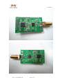
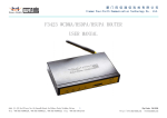
F8913 ZigBee data transmission module is based on the IEEE 802.15.4/ZigBee
technology,embedded wireless data transmission module, use the 2.4GHz IEEE 802.15.4
standard RF transceivers for ZigBee networks to provide users with wireless data
transmission capabilities.
The product uses high-performance industrial grade ZigBee program can work on the
toll-free worldwide 2.4GHz ISM(Industrial,Scientific and Medical)band, and is divided into
16 channels in the band, the data transfer rate of 250kb/s.In addition to the IEEE
standards-based RF and PHY/MAC layer protocol stack embedded F8913 supports a
variety of network functions. From simple lighting networks to complex multi-layer Ad-Hoc
private network,F8913 network to support design can cover the entire range of needs.
It has been widely used on M2M fields, such as intelligent transportation, smart grid,
industrial automation, telemetry, finance, POS, water supply, environment protection, post,
weather, and so on.
1.2 Specifications
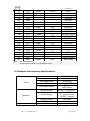
1.2.1、F8913-N and F8913-E Specifications
Specifications of the F8914-N/F8914-E ZB SMT RF Module
Specification
F8913-N
F8913-E
Outdoor RF line-of-sight Range
200 米
800 米
Indoor/Urban Range
60 米
90 米
Transmit Power Output
1.26mw(1dBm), Normal mode
100 mw (+20dBm)
2.82mw (+4.5dBm), Boost mode
250kbps
RF Data Rate
-50 dBm(Normal mode)
-95dBm(Boost mode)
Receiver Sensitivity
-104dBm
2.0~3.6V
Supply Voltage
Operating Current (Transmit))
29mA(+1dBm, Normal mode)
34mA(+4.5dBm, Boost mode)
128mA@+3.0V,+20dBm
Operating Current (Receive)
20.5mA(Normal mode)
24.3mA(Boost mode)
25mA
Power-down Current
<1uA@25°C
Operating Frequency Band
ISM2.4~2.5GHz
ZigBee Standard
IEEE 802.15.4
Dimensions
0.875” x 1.475” x 0.149” (2.223cm x 3.747cm x 0.378cm)
http://www.fourfaith.com
Page 5 of 27
User Manual
Weight
38g
40g
Operating Temperature
-40~125ºC
-40~85ºC
Standard SMA female interface、U.FL Connector
Antenna Options
Pin Interface
SMT2.0 Patch、line-double 8 spacing of 2.0
Supported Network Topologies
Point-to-point, Point-to-multipoint, Peer-to-peer, and Mesh
Number of Channels
16 Direct Sequence Channels
Channels
11~26
Max packge size
512Bytes
Node Type
Coordinator、Route、Endpoints (optional)
UART
9600、19200、38400、57600、115200 bps
SPI
4 Mbps maximum (burst)
Protocol Standards
ZigBee Pro
1.2.2 Serial Communications Specifications
F8913 RF modules support both UART (Universal Asynchronous Receiver /
Transmitter) and SPI (Serial Peripheral Interface) serial connections.
1.2.2.1 UART
The SC1 (Serial Communication Port 1) of the CC2530 is connected to the
UART port.
UART Pin Assignments
UART Pins
Module Pin Number
TX
25(SMT)、41(DIP)
RX
26(SMT)、40(DIP)
CT/ADC/GPIO
24(SMT)、19(DIP)
RT/ADC/GPIO
23(SMT)、18(DIP)
More information on UART operation is found in the UART section in Chapter 2.
1.2.2.2 SPI
The SC2 (Serial Communication Port 2) of the CC2530 is connected to the SPI
port.
SPI Pin Assignments
SPI Pins
Module Pin Number
MI/GPIO
9(SMT)、14(DIP)
MO/GPIO
10(SMT)、15(DIP)
http://www.fourfaith.com
Page 6 of 27
User Manual
C/GPIO
11(SMT)、16(DIP)
SS/GPIO
12(SMT)、17(DIP)
For more information on SPI operation, see the SPI section in Chapter 2.
1.2.3 GPIO Specifications
F8913 RF modules have 21 GPIO (General Purpose Input / Output) ports
available. The exact list will depend on the module configuration, as some GPIO pads
are used for purposes such as serial communication. See GPIO section for more
information on configuring and using GPIO ports.
Electrical Specifications for GPIO Pads
GPIO Electrical Specification
Voltage – Supply(V)
MIN
TYP
MAX
-0.3
VDD
+0.3
0.5
Logic-0 input voltage(V)
Logic-1 input voltage(V)
2.5
Logic-0 input current(A)
-50
50
Logic-1 input current(A)
-50
50
Input pull-up and pull-down resistor
value(kΩ )
20
0.5
Logic-0 output voltage, 4-mA pins(V)
Logic-1 output voltage, 4-mA pins(V)
2.4
0.5
Logic-0 output voltage, 20-mA pins(V)
Logic-1 output voltage, 20-mA pins(V)
2.4
Note: The output drive strength is 4 mA on all outputs, except for the two high-drive
outputs, P1.0 and P1.1,which each have 20-mA output drive strength.
http://www.fourfaith.com
Page 7 of 27
User Manual
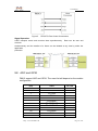
1.3 Module Pin Definition
Top View
Pin No
SMT
1
2
3
4
5
6
7
8
9
10
11
12
13
22
23
24
25
26
27
28
29
30
31
32
Botton View
Symbol
Direction
Default Function
Description
GND
VCC
GND
P2.4
P2.3
P2.2
P2.1
P2.0
P1.7
P1.6
P1.5
P1.4
P1.3
P0.6
P0.5
P0.4
P0.3
P0.2
P0.1
P0.0
RST
P1.1
P1.2
P0.7
Input
Output
Input
Both
Both
Output
Input
Input
Input
Both
Input
Input
Output
Output
Input
Input
Input
Input
Both
Both
Both
Q1
Q2
DC
DD
GPIO
MI
MO
C
SS
GPIO
ADC
RT
CT
TX
RX
ADC
ADC
Reset
-
Ground
Power Supply
Ground
XOSC32K_Q1
XOSC32K_Q2
DC/GPIO
DD/GPIO
GPIO
MI/GPIO
MO/GPIO
C/GPIO
SS/GPIO
GPIO
ADC/GPIO
RT/ADC/GPIO
CT/ADC/GPIO
TX
RX
ADC/GPIO
ADC/GPIO
Module Reset
GPIO
GPIO
GPIO
http://www.fourfaith.com
Page 8 of 27
User Manual
33
P1.0
34
GND
35
VCC
36
GND
37
GND
DIP
14
P1.7
15
P1.6
16
P1.5
17
P1.4
18
P0.5
19
P0.4
20
P0.1
21
P0.0
38
P2.2
39
P2.1
40
P0.2
41
P0.3
42
RST
43
GND
44
VCC
45
P0.6
Note: Red F8913-N have.
Both
-
GPIO
-
GPIO
Ground
Power Supply
Ground
Ground
Output
Input
Input
Input
Input
Output
Input
Input
Input
Both
Both
Both
Input
Input
MI
MO
C
SS
RT
CT
ADC
ADC
DC
DD
RX
TX
Reset
ADC
MI/GPIO
MO/GPIO
C/GPIO
SS/GPIO
RT/ADC/GPIO
CT/ADC/GPIO
ADC/GPIO
ADC/GPIO
DC/GPIO
DD/GPIO
RX
TX
Module Reset
Ground
Power Supply
ADC/GPIO
Signal direction relative to the specified module.
1.4 Firmware Performance Specifications
Serial
Baud
Configuration
Max packge size
XOR
Command Mode
Network Max
Network
Sleep
http://www.fourfaith.com
Node Range
Routing Table
RREQ Table
External Wake-Up
115200(Default)
8/N/1
512Bytes
1-byte XOR
AT Mode
HEX Mode
65000(0~65000)
0~65000
0:Coordinator Add
65535:Broad
180-way
4-way
RTC Wake-up
Page 9 of 27
User Manual
1.5 Absolute Maximum Ratings
Supply voltage
All supply pins must have the same voltage
MIN
MAX
-0.3
3.9
V
+0.3
≤3.9
V
10
dBm
125
°C
2
KV
-0.3
Voltage on any digital pin
VDD
Input RF level
–40
Storage temperature range
ESD(2)
All pads, according to human-body model, JEDEC STD 22, method A114
According to charged-device model, JEDEC STD 22, method C101
UNIT
500
V
NOTE:
(1)
Stresses beyond those listed under Absolute Maximum Ratings may cause permanent damage to the device.
These are stress ratings only, and functional operation of the device at these or any other conditions beyond
those indicated under Recommended Operating Conditions is not implied. Exposure to absolute-maximum-rated
conditions for extended periods may affect device reliability.
(2)
CAUTION: ESD sensitive device. Precaution should be used when handling the device in order to prevent
ermanent damage.
Chapter 2
Module Operation
2.1 Serial communication
Signal Description
Default UART Transport
UART default configuration :
Baud rate: 115200
8-N-1 byte format
The following standard UART signals are used:
TX: Transmit data.
RX: Receive data.
CT: Clear to send.
RT: Ready to send.
Figure 5 shows the RTS/CTS flow control connections to the host processor. On the
CC2530, RT and CT are active-low signals. The RT output is driven low when the receive
register is empty and reception is enabled. Transmission of a byte does not occur before
the CT input goes low.
http://www.fourfaith.com
Page 10 of 27
User Manual
Figure 5
RTS/CTS Flow Control Connections
Signal Operation
UART transport sends and receives data asynchronously. Data can be sent and
received
simultaneously and the transfer of a frame can be initiated at any time by either the
application
processor
2.2 ADC and GPIO
F8913 support ADC and GPIO, The exact list will depend on the module
configuration.
Pins
name
AT cmd
SMT
6
7
8
13
22
23
24
27
28
33
P2.2/DC
P2.1/DD
P2.0
P1.3
P0.6/ADC
P0.5/RT/ADC
P0.4/CT/ADC
P0.1/ADC
P0.0/ADC
P1.0
DIP
http://www.fourfaith.com
Page 11 of 27
User Manual
P0.5/RT/ADC
P0.4/CT/ADC
P0.1/ADC
P0.0/ADC
P2.2/DC
P2.1/DD
P0.6/ADC
18
19
20
21
38
39
45
I/O Configuration
See AT command “AT+DMn” section in charpter 3
Setting value
Description
0
Disabled
1
Analog
2
Data in monitored
3
Data out low
4
Data out high
Chapter 3 Configuration
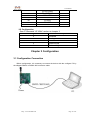
3.1 Configuration Connection
Before configuration, It’s necessary to connect the device with the configure PC by
the shipped RS232 or RS232-485 conversion cable.
http://www.fourfaith.com
Page 12 of 27
User Manual
3.2 Configuration Introduction
There are two ways to configure the F8913:
Configuration software tool: All the settings are configured through the shipped
software tool. It’s necessary to have one PC to run this tool.
Extended AT command: All the settings are configured through AT command, so any
device with serial port can configure it. Before configuration with AT command, you
should make F8913 enter configure state.
The following describes how to configure F8913 with the configure software tool. At the
same time, it gives out the corresponding AT command of each configuration item.
3.3 Run the configure Tool: ZigbeeConfigure.exe
The “Serial Parameters” column shows the current serial port settings. To configure IP
MODEM, please choose the correct serial port which connects to F8913, and the
baud-rate is 115200 with no parity, then open the serial port. If the button text is“Close”, it
shows the serial port now has been opened. If the text is “Open”, you should open the port
first. When the port opened, the “Output Info” column will display
“Port(COM1) Has Opened,Please Re-Power the F8913,
Waiting F8913 enter configure state...”
http://www.fourfaith.com
Page 13 of 27
User Manual
3.4 Re-power F8913
After Re-power F8913, The configure tool will make it enter configure state. At the
same time, the software will load current settings from and displays on the right configure
columns. It’s now ready to configure.
3.5 Configuration
Acronyms :
SREQ : Asynchronous Request
SREQ : Synchronous request
SRSP : Synchronous response
1
Transparent mode.
In transparent mode, F8913 received data from serial interface, then send
data to other zigbee device by RF according to the address of the transparent
transmit address. See AT command AT+TID
2
AT command mode
When In transparent mode,Enter 3 equal mark "+++" twice in 100
mSecondsto place the F8913 in API mode.
AT+<command>?<CR LF>
AT+<command>=<value><CR LF>
Success response : OK<CR LF>
Failure response : ERROR<CR LF>
CR: 0x0D
carriage return
LF: 0x0A
line feed
Example:
Query:AT+PID?<CR LF>
rsp:+PID:0<CR LF>
OK<CR LF>
Setting:AT+PID=198<CR LF>
rsp:OK<CR LF>
Query value
Setting value
ATcommand:
AT+PID
PAN ID setting
PAN ID digital string 0-65535
0-16383: Set a PAN ID.
65535 : System will assign a stochastic PAN ID. (default)
Query rsp:
+PID:65535
http://www.fourfaith.com
Page 14 of 27
User Manual
OK
Note: This command setting the PID that saving in non-valatile flash.
In contrast ,“AT+PCD” command query the PANID which is used
actually
AT+PCD
Query the current used PANID
example:
AT+PCD?
Query rsp:
+PCD:65535
OK
AT+MID
MAC Address
16 HEX characters
example:0x0123456789ABCDEF.
[read only]
Query rsp:
+MID:EF357F01004B1200
OK
AT+TYP=<0,1,2>
Node Type
(0 -- Coordinator,
1 -- Router (defalut)
2 -- End Device)
+TYP:0
OK
AT+NID
Node Address
(0-65535)
NOTE: when Coordinator establish a network,its net address will be
0,only a coordinator in the network.
Router and End device shold not set network address to 0
65535 System will assign a stochastic net address
Query rsp:
+NID:65535
OK
Note: This command setting the PID that saving in non-valatile flash.
In contrast ,“AT+NCD” command query the net address which is used
actually
AT+NCD
example:
AT+NCD?
Query rsp:
http://www.fourfaith.com
Page 15 of 27
User Manual
+NCD:65535
OK
AT+TID
Transparent Address
0-65535 (0 dafault)
65535 is broadcast address. It will send to all other nodes.
Query rsp:
+TID:0
OK
AT+IPR
Baud Rate
0 -- 9600
1 -- 19200
2 -- 38400
3 – 57600
4 — 115200
(dafault)
AT+ECH
character
0 -- no character echo
1 -- character echo
(0-4)
echo.
AT+ACK=<0,1> data acknowledgement.
0-- NO
1-- YES (dafault)
AT+VER
Version
Query rsp:
Four-Faith F8913 Standard
Ver: V1.00
Time: Nov 28 2011 16:02:38
OK
AT+DBL=<0,1,2>
log level.
0 -- disable
(dafault)
1 -- print significant message.
2 -- print all message.
AT+AST=<0,1>
auto go into network when power on
0 -- no
1 -- yes. (dafault)
AT+STA
Success : OK
Start network.
http://www.fourfaith.com
Page 16 of 27
User Manual
failure :ERROR
note: when AT+AST=0,use this command to start network.
AT+CHA=<11-26>
Set Working Channel
AT+SAV
Save all setting parameters to System.
AT+ESC
Escape, exit AT command mode, and enter the transparent
mode.
AT+API
API
switch to API mode
AT+FAC
Factory
load factory setting
AT+SRS
System Reset
AT+SNS
Query network state or itself.
RSP:+SNS:01
OK
net state table:
00
Initialized - not started automatically
01
Initialized - not connected to anything
02
Discovering PAN's to join
03
Joining a PAN
04
ReJoining a PAN, only for end devices
05
Joined but not yet authenticated by trust
center
06
Started as device after authentication
07
Device joined, authenticated and is a router
08
Zigbee Coordinator starting network
09
Started as Zigbee Coordinator
10
Device has lost information about its parent
AT+NWS
For coordinator to query the whole network state.
SRSP:
rsp:
OK
then receive other node's response.
+NWS:<state>,<net address>,<IEEE address >,<node type>
Example:
+NWS:0,1,1122334455667788,0
+NWS:0,2,1122334455667799,1
+NWS:0,8,1122334455667732,2
NOTE: For avoid network busy traffic,other nodes receiving this OTA
command will delay a random time, and then sent response to
coordinator.Random time range: 0--66 seconds
AT+QNA=<MAC address>
SRSP:
Success rsp:
http://www.fourfaith.com
query net addrss by MAC address.
Page 17 of 27
User Manual
OK
Failure rsp:
ERROR
AREQ:
+NWS:<state>,<net address>,<IEEE address >,<node type>
AT+QMA=<Net address>
Query MAC address by net address.
SRSP:
Success rsp:
OK
Failure rsp:
ERROR
AREQ:
+NWS:<state>,<net address>,<IEEE address >,<node type>
AT data send and receive
HEX mode: AT+TXH=< destination address(little endidan)><data content>
send data:
AT+TXH=0123383838383838
destination net address: 0x2301
data content: "888888"
SRSP:
OK
ASCII mode:
Send data:
AT+TXA=12245,1235567789
destination address: 12245
data content: "1235567789"
Receive data
AREQ:
:+RCV:12245,1235567789
Source net address: 12245
data content: "1235567789"
OTA IO Sample and control
AT+DMn=<0-5>
0 = Disabled
1 = ADC
2 = DI
3 = DO low
4 = DO high
example:AT+DM1=4
http://www.fourfaith.com
IO work mode setting
GPIO input
GPIO ouput High
GPIO ouput High
Page 18 of 27
User Manual
AT+DTn=<0-65535 seconds>
auto report time interval setting.
0
-- diable
others -- F8913 will report IO value to coordinator per
interval time
AT+DVn?
Example:
AT+DV3?
rsp:
+DV3:1
OK
get IO value
AT+NVn=<net address>
OTA query
SRSP:
Sucess rsp:OK
Failure rsp:ERROR
AREQ:
Sucess rsp:
+NVn:<state>,<destination net address>,<value>
Failure rsp:
+NVn:<state>,< destination net address >,<value>
状态信息表:
0
Success
1
no in the newwork
2
no exist
3
no ack
4
IO no used
5
invalid value
OTA IO Set.
AT+NSn=<net address>,<mode 3 or 4>
Description: Set IO output only when IO mode is Hight or Low
3 API work mode:
Enter API mode:
When In transparent mode,Enter 3 equal mark "===" twice to place the
F8913 in API mode.
When In AT command mode,send AT+API command to place the F8913 in
API
http://www.fourfaith.com
Page 19 of 27
User Manual
mode:
AT+API<CR><LF>
Exit API mode:
refer to API command Set work mode
General Frame Format. The general frame format is shown in the following
figure. The left-most field is transmitted first
over the wire. For multi-byte fields, the lowest order byte is transmitted first:
SOF
1 Byte
Length
1 Byte
Command Data
2 Bytes
xx Bytes (xx<250)
FCS
1 Byte
SOF: Start of frame indicator. This is always set to 0xFE
Length: The length of the data field of the frame.
Command: The command of the frame.
Data: The frame data. This depends on the command field and is
described for each command.
FCS: Frame-check sequence. This field is computed as an XOR of all the
bytes in the length,command and data fields.
Shown below is a C example for the FCS calculation:
unsigned char calcFCS(unsigned char *pMsg, unsigned char len)
{
unsigned char result = 0;
while (len--)
{
result ^= *pMsg++;
}
return result;
}
Data send.
SREQ:
Fields
Sub Fields
SOF
Length
Command Data send
Data
Address
Content
FCS
Offset
1
1
2
2
4
1
Example
FE
06
24 5F
00 00
41 41 41 41
Description
SRSP:
Fields
SOF
Length
Offset
1
1
Example
FE
03
Description
Sub Fields
http://www.fourfaith.com
Destination address
Page 20 of 27
User Manual
Command
Data
state
FCS
2
1
1
64 5F
00
AREQ:
Fields
Sub Fields
SOF
Length
Command
Data
state
Offset
1
1
2
1
Example
FE
03
44 80
00
00
Description
00 -- success
others -- error
0B 00
FCS
1
Receive data
AREQ:
Fields
Sub Fields
SOF
Length
Command
Data
source
address
content
FCS
Offset
1
1
2
2
Example
FE
06
44 5F
00 00
Description
<80
1
42 42 42 42
content
Set work mode
SREQ:
Fields
Sub Fields
SOF
Length
Command mode set
Data
mode value
Offset
1
1
2
1
Example
FE
01
21 2A
00
Description
FCS
1
Example
FE
01
Description
SRSP:
Fields
SOF
Length
Sub Fields
http://www.fourfaith.com
Offset
1
1
Source net address
work mode
0 – transparent mode
1 – AT command mode
2 – API mode
Page 21 of 27
User Manual
Command mode set ack
Data
state
2
1
61 2A
00
FCS
1
OTA IO Sample
SREQ(24 5E):
Fields
Sub Fields
SOF
Length
Command
Data
Des address
read action
IO address
FCS
Offset
1
1
2
2
1
1
1
Example
FE
04
24 5E
00 00
00
02
Description
SRSP(64 5E):
Fields
Sub Fields
SOF
Length
Command
Data
state
FCS
Offset
1
1
2
1
1
Example
FE
06
64 5E
Description
ARSP(44 5E):
Fields
Sub Fields
SOF
Length
Command
Data
state
Des address
IO address
IO value
FCS
Offset
1
1
2
1
2
1
n
1
Example
FE
06
44 5E
00
00 00
2
12 34
Destination address
IO address (00 - 02)
state
OTA Pin Set(Only in GPIO output mode)
SREQ:
Fields
Sub Fields
Offset Example
SOF
1
FE
Length
1
03
Command
2
24 60
Data
Des address
2
00 01
write action
1
01
http://www.fourfaith.com
0 -- success
1-- error
Description
state
Destination address
Destination IO address
value is 0x3412
Description
Destination address
Page 22 of 27
User Manual
IO address
IO value
02
01 00
Destination IO address
0x0001(little endian)
FCS
1
1
1
SRSP:
Fields
Sub Fields
SOF
Length
Command
Data
state
FCS
Offset
1
1
2
1
1
Example
FE
06
64 60
Description
ARSP:
Fields
Sub Fields
SOF
Length
Command
Data
state
Des address
IO address
state
Offset
1
1
2
1
2
1
1
Example
FE
05
44 60
00
00 00
2
00
Description
FCS
1
OTA IEEE address query
SREQ:
Fields
Sub Fields
SOF
Length
Command
Data
Des address
action
FCS
Offset
1
1
2
2
1
1
Example
FE
02
24 5D
12 34
02
Description
SRSP
Fields
Sub Fields
SOF
Length
Command
Data
state
FCS
Offset
1
1
2
1
1
Example
FE
01
64 5D
00
Description
http://www.fourfaith.com
state
Destination address
Destination IO address
00 -- success
othters -- error
Destination address
IEEE address query
state
Page 23 of 27
User Manual
AREQ:
Fields
Sub Fields
SOF
Length
Command
Data
state
Source
address
IEEE address
node type
Offset
1
1
2
1
2
Example
FE
0C
44 5D
0
00 00
Description
8
12 34 56 78
AA BB CC
DD
0xDDCCBBAA78563412
1
FCS
1
OTA net address query
SREQ:
Fields
Sub Fields
SOF
Length
Command
Data
action
IEEE address
Offset
1
1
2
1
8
FCS
1
SRSP:
Fields
Sub Fields
SOF
Length
Command
Data
state
FCS
Offset
1
1
2
1
1
state
Source netaddress
0 -- Cordinator
1 -- Router
2 – End device
Example
FE
09
24 5C
03
12 34 56 78
AA BB CC
DD
Example
FE
01
64 5C
00
Description
(Its is a broadcast cmd)
qurey net address
0xDDCCBBAA78563412
Description
state
AREQ:
Same as the AREQ of OTA IEEE netaddres query
OTA query the whole network
SREQ:
http://www.fourfaith.com
Page 24 of 27
User Manual
Fields
Sub Fields
SOF
Length
Command
Data
-FCS
Offset
1
1
2
1
1
Example
FE
01
24 5B
01
Description
SRSP:
Fields
Sub Fields
SOF
Length
Command
Data
state
FCS
Offset
1
1
2
1
1
Example
FE
03
64 5B
00
Description
state
AREQ:
Same as the AREQ of OTA IEEE netaddres query
Chapter 4 Hardware Specifications
4.1 F8913 Module Mechanical Dimensions
We recommend that you use as shown below for the
surface-mount PCB packaging. Dimensions are in millimeters.
http://www.fourfaith.com
Page 25 of 27
User Manual
You can also use the DIP PCB package as shown below.
Dimensions are in millimeters.
4.2 Re-flow Temperature Specification
Recommendations according to IPC / JEDEC J-STD-020B
standard welding.
http://www.fourfaith.com
Page 26 of 27
User Manual
4.3 Solder Recommended
Recommendations according to IPC / JEDEC J-STD-020B
standard welding.
Chapter 5 Ordering Information
You can contact Xiamen Four-Faith Communication Technology
Co., Ltd. and our sales to buy modules or development kit to expand
your network. Please specify date you need the product model.
http://www.fourfaith.com
Page 27 of 27