1
DAQ
NI 653X User Manual for Traditional NI-DAQ
High-Speed Digital I/O Devices for PCI, PXI, CompactPCI, AT, EISA,
and PCMCIA Bus Systems
NI 653X User Manual
February 2005
371464D-01
Support
Worldwide Technical Support and Product Information
ni.com
National Instruments Corporate Headquarters
11500 North Mopac Expressway
Austin, Texas 78759-3504
USA Tel: 512 683 0100
Worldwide Offices
Australia 1800 300 800, Austria 43 0 662 45 79 90 0, Belgium 32 0 2 757 00 20, Brazil 55 11 3262 3599,
Canada 800 433 3488, China 86 21 6555 7838, Czech Republic 420 224 235 774, Denmark 45 45 76 26 00,
Finland 385 0 9 725 725 11, France 33 0 1 48 14 24 24, Germany 49 0 89 741 31 30, India 91 80 51190000,
Israel 972 0 3 6393737, Italy 39 02 413091, Japan 81 3 5472 2970, Korea 82 02 3451 3400,
Lebanon 961 0 1 33 28 28, Malaysia 1800 887710, Mexico 01 800 010 0793, Netherlands 31 0 348 433 466,
New Zealand 0800 553 322, Norway 47 0 66 90 76 60, Poland 48 22 3390150, Portugal 351 210 311 210,
Russia 7 095 783 68 51, Singapore 1800 226 5886, Slovenia 386 3 425 4200, South Africa 27 0 11 805 8197,
Spain 34 91 640 0085, Sweden 46 0 8 587 895 00, Switzerland 41 56 200 51 51, Taiwan 02 2377 2222,
Thailand 662 992 7519, United Kingdom 44 0 1635 523545
For further support information, refer to the Technical Support and Professional Services appendix. To comment
on National Instruments documentation, refer to the National Instruments Web site at ni.com/info and enter
the info code feedback.
© 1997–2005 National Instruments Corporation. All rights reserved.
Important Information
Warranty
The NI AT-DIO-32HS, NI DAQCard-6533 for PCMCIA, NI PCI-6534, NI PCI-DIO-32HS, NI PXI-6533, and NI PXI-6534 devices are
warranted against defects in materials and workmanship for a period of one year from the date of shipment, as evidenced by receipts or other
documentation. National Instruments will, at its option, repair or replace equipment that proves to be defective during the warranty period. This
warranty includes parts and labor.
The media on which you receive National Instruments software are warranted not to fail to execute programming instructions, due to defects
in materials and workmanship, for a period of 90 days from date of shipment, as evidenced by receipts or other documentation. National
Instruments will, at its option, repair or replace software media that do not execute programming instructions if National Instruments receives
notice of such defects during the warranty period. National Instruments does not warrant that the operation of the software shall be
uninterrupted or error free.
A Return Material Authorization (RMA) number must be obtained from the factory and clearly marked on the outside of the package before
any equipment will be accepted for warranty work. National Instruments will pay the shipping costs of returning to the owner parts which are
covered by warranty.
National Instruments believes that the information in this document is accurate. The document has been carefully reviewed for technical
accuracy. In the event that technical or typographical errors exist, National Instruments reserves the right to make changes to subsequent
editions of this document without prior notice to holders of this edition. The reader should consult National Instruments if errors are suspected.
In no event shall National Instruments be liable for any damages arising out of or related to this document or the information contained in it.
EXCEPT AS SPECIFIED HEREIN, NATIONAL INSTRUMENTS MAKES NO WARRANTIES, EXPRESS OR IMPLIED, AND SPECIFICALLY DISCLAIMS ANY WARRANTY OF
MERCHANTABILITY OR FITNESS FOR A PARTICULAR PURPOSE. CUSTOMER’S RIGHT TO RECOVER DAMAGES CAUSED BY FAULT OR NEGLIGENCE ON THE PART OF
NATIONAL INSTRUMENTS SHALL BE LIMITED TO THE AMOUNT THERETOFORE PAID BY THE CUSTOMER. NATIONAL INSTRUMENTS WILL NOT BE LIABLE FOR
DAMAGES RESULTING FROM LOSS OF DATA, PROFITS, USE OF PRODUCTS, OR INCIDENTAL OR CONSEQUENTIAL DAMAGES, EVEN IF ADVISED OF THE POSSIBILITY
THEREOF. This limitation of the liability of National Instruments will apply regardless of the form of action, whether in contract or tort, including
negligence. Any action against National Instruments must be brought within one year after the cause of action accrues. National Instruments
shall not be liable for any delay in performance due to causes beyond its reasonable control. The warranty provided herein does not cover
damages, defects, malfunctions, or service failures caused by owner’s failure to follow the National Instruments installation, operation, or
maintenance instructions; owner’s modification of the product; owner’s abuse, misuse, or negligent acts; and power failure or surges, fire,
flood, accident, actions of third parties, or other events outside reasonable control.
Copyright
Under the copyright laws, this publication may not be reproduced or transmitted in any form, electronic or mechanical, including photocopying,
recording, storing in an information retrieval system, or translating, in whole or in part, without the prior written consent of National
Instruments Corporation.
Trademarks
National Instruments, NI, ni.com, and LabVIEW are trademarks of National Instruments Corporation. Refer to the Terms of Use section
on ni.com/legal for more information about National Instruments trademarks.
Other product and company names mentioned herein are trademarks or trade names of their respective companies.
Members of the National Instruments Alliance Partner Program are business entities independent from National Instruments and have no
agency, partnership, or joint-venture relationship with National Instruments.
Patents
For patents covering National Instruments products, refer to the appropriate location: Help»Patents in your software, the patents.txt file
on your CD, or ni.com/patents.
WARNING REGARDING USE OF NATIONAL INSTRUMENTS PRODUCTS
(1) NATIONAL INSTRUMENTS PRODUCTS ARE NOT DESIGNED WITH COMPONENTS AND TESTING FOR A LEVEL OF
RELIABILITY SUITABLE FOR USE IN OR IN CONNECTION WITH SURGICAL IMPLANTS OR AS CRITICAL COMPONENTS IN
ANY LIFE SUPPORT SYSTEMS WHOSE FAILURE TO PERFORM CAN REASONABLY BE EXPECTED TO CAUSE SIGNIFICANT
INJURY TO A HUMAN.
(2) IN ANY APPLICATION, INCLUDING THE ABOVE, RELIABILITY OF OPERATION OF THE SOFTWARE PRODUCTS CAN BE
IMPAIRED BY ADVERSE FACTORS, INCLUDING BUT NOT LIMITED TO FLUCTUATIONS IN ELECTRICAL POWER SUPPLY,
COMPUTER HARDWARE MALFUNCTIONS, COMPUTER OPERATING SYSTEM SOFTWARE FITNESS, FITNESS OF COMPILERS
AND DEVELOPMENT SOFTWARE USED TO DEVELOP AN APPLICATION, INSTALLATION ERRORS, SOFTWARE AND
HARDWARE COMPATIBILITY PROBLEMS, MALFUNCTIONS OR FAILURES OF ELECTRONIC MONITORING OR CONTROL
DEVICES, TRANSIENT FAILURES OF ELECTRONIC SYSTEMS (HARDWARE AND/OR SOFTWARE), UNANTICIPATED USES OR
MISUSES, OR ERRORS ON THE PART OF THE USER OR APPLICATIONS DESIGNER (ADVERSE FACTORS SUCH AS THESE ARE
HEREAFTER COLLECTIVELY TERMED “SYSTEM FAILURES”). ANY APPLICATION WHERE A SYSTEM FAILURE WOULD
CREATE A RISK OF HARM TO PROPERTY OR PERSONS (INCLUDING THE RISK OF BODILY INJURY AND DEATH) SHOULD
NOT BE RELIANT SOLELY UPON ONE FORM OF ELECTRONIC SYSTEM DUE TO THE RISK OF SYSTEM FAILURE. TO AVOID
DAMAGE, INJURY, OR DEATH, THE USER OR APPLICATION DESIGNER MUST TAKE REASONABLY PRUDENT STEPS TO
PROTECT AGAINST SYSTEM FAILURES, INCLUDING BUT NOT LIMITED TO BACK-UP OR SHUT DOWN MECHANISMS.
BECAUSE EACH END-USER SYSTEM IS CUSTOMIZED AND DIFFERS FROM NATIONAL INSTRUMENTS' TESTING
PLATFORMS AND BECAUSE A USER OR APPLICATION DESIGNER MAY USE NATIONAL INSTRUMENTS PRODUCTS IN
COMBINATION WITH OTHER PRODUCTS IN A MANNER NOT EVALUATED OR CONTEMPLATED BY NATIONAL
INSTRUMENTS, THE USER OR APPLICATION DESIGNER IS ULTIMATELY RESPONSIBLE FOR VERIFYING AND VALIDATING
THE SUITABILITY OF NATIONAL INSTRUMENTS PRODUCTS WHENEVER NATIONAL INSTRUMENTS PRODUCTS ARE
INCORPORATED IN A SYSTEM OR APPLICATION, INCLUDING, WITHOUT LIMITATION, THE APPROPRIATE DESIGN,
PROCESS AND SAFETY LEVEL OF SUCH SYSTEM OR APPLICATION.
Compliance
Compliance with FCC/Canada Radio Frequency Interference
Regulations
Determining FCC Class
The Federal Communications Commission (FCC) has rules to protect wireless communications from interference. The FCC
places digital electronics into two classes. These classes are known as Class A (for use in industrial-commercial locations only)
or Class B (for use in residential or commercial locations). All National Instruments (NI) products are FCC Class A products.
Depending on where it is operated, this Class A product could be subject to restrictions in the FCC rules. (In Canada, the
Department of Communications (DOC), of Industry Canada, regulates wireless interference in much the same way.) Digital
electronics emit weak signals during normal operation that can affect radio, television, or other wireless products.
All Class A products display a simple warning statement of one paragraph in length regarding interference and undesired
operation. The FCC rules have restrictions regarding the locations where FCC Class A products can be operated.
Consult the FCC Web site at www.fcc.gov for more information.
FCC/DOC Warnings
This equipment generates and uses radio frequency energy and, if not installed and used in strict accordance with the instructions
in this manual and the CE marking Declaration of Conformity*, may cause interference to radio and television reception.
Classification requirements are the same for the Federal Communications Commission (FCC) and the Canadian Department
of Communications (DOC).
Changes or modifications not expressly approved by NI could void the user’s authority to operate the equipment under the
FCC Rules.
Class A
Federal Communications Commission
This equipment has been tested and found to comply with the limits for a Class A digital device, pursuant to part 15 of the FCC
Rules. These limits are designed to provide reasonable protection against harmful interference when the equipment is operated
in a commercial environment. This equipment generates, uses, and can radiate radio frequency energy and, if not installed and
used in accordance with the instruction manual, may cause harmful interference to radio communications. Operation of this
equipment in a residential area is likely to cause harmful interference in which case the user is required to correct the interference
at their own expense.
Canadian Department of Communications
This Class A digital apparatus meets all requirements of the Canadian Interference-Causing Equipment Regulations.
Cet appareil numérique de la classe A respecte toutes les exigences du Règlement sur le matériel brouilleur du Canada.
Compliance with EU Directives
Users in the European Union (EU) should refer to the Declaration of Conformity (DoC) for information* pertaining to the
CE marking. Refer to the Declaration of Conformity (DoC) for this product for any additional regulatory compliance
information. To obtain the DoC for this product, visit ni.com/certification, search by model number or product line,
and click the appropriate link in the Certification column.
* The CE marking Declaration of Conformity contains important supplementary information and instructions for the user or
installer.
Conventions
The following conventions appear in this manual:
<>
Angle brackets that contain numbers separated by an ellipsis represent a
range of values associated with a bit or signal name—for example,
DIO<3..0>.
»
The » symbol leads you through nested menu items and dialog box options
to a final action. The sequence File»Page Setup»Options directs you to
pull down the File menu, select the Page Setup item, and select Options
from the last dialog box.
♦
The ♦ symbol indicates that the following text applies only to a specific
product, a specific operating system, or a specific software version.
This icon denotes a tip, which alerts you to advisory information.
This icon denotes a note, which alerts you to important information.
This icon denotes a caution, which advises you of precautions to take to
avoid injury, data loss, or a system crash. When this symbol is marked on a
product, refer to the for information about precautions to take.
bold
Bold text denotes items that you must select or click in the software, such
as menu items and dialog box options. Bold text also denotes parameter
names.
italic
Italic text denotes variables, emphasis, a cross reference, or an introduction
to a key concept. This font also denotes text that is a placeholder for a word
or value that you must supply.
monospace
Text in this font denotes text or characters that you should enter from the
keyboard. This font is also used for the proper names of functions,
variables, and filenames and extensions.
NI 6533
NI 6533 refers to the NI AT-DIO-32HS, NI DAQCard-6533 for PCMCIA,
NI PCI-DIO-32HS, and NI PXI-6533 devices, unless otherwise noted.
NI 6534
NI 6534 refers to the NI PCI-6534 and NI PXI-6534 devices, unless
otherwise noted.
NI 653X
NI 653X refers to the NI AT-DIO-32HS, NI DAQCard-6533 for PCMCIA,
NI PCI-6534, NI PCI-DIO-32HS, NI PXI-6533, and NI PXI-6534 devices,
unless otherwise noted.
Contents
Chapter 1
Getting Started with Your NI 653X
NI 653X Overview ........................................................................................................1-1
Control Lines ...................................................................................................1-2
What You Need to Get Started ......................................................................................1-2
Choosing Your Programming Software ........................................................................1-3
National Instruments Application Software ....................................................1-3
NI-DAQ Driver Software ................................................................................1-4
Installing Your Software................................................................................................1-6
Unpacking Your NI 653X ..............................................................................................1-6
Installing Your NI 653X ................................................................................................1-7
Installing the NI PCI-DIO-32HS, NI PCI-6534, or NI PCI-7030/6533..........1-7
Installing the NI PXI-6533, NI PXI-6534, or NI PXI-7030/6533...................1-7
Installing the NI AT-DIO-32HS......................................................................1-8
Installing the NI DAQCard-6533 for PCMCIA ..............................................1-9
Configuring the NI 653X ...............................................................................................1-9
In Windows .....................................................................................................1-9
In Mac OS........................................................................................................1-10
Safety Information .........................................................................................................1-10
Chapter 2
Using Your NI 653X
Choosing the Correct Mode for Your Application ........................................................2-1
Controlling and Monitoring Static Digital Lines—Unstrobed I/O ................................2-2
Configuring Digital Lines................................................................................2-2
Standard Output ................................................................................2-2
Open-Collector Output......................................................................2-2
Using Control Lines as Extra Unstrobed Data Lines ......................................2-3
Connecting Signals..........................................................................................2-4
Creating a Program..........................................................................................2-4
Programming the Control/Timing Lines as Extra Unstrobed
Data Lines ......................................................................................2-5
Generating and Receiving Digital Patterns and Waveforms—Pattern I/O....................2-6
Deciding the Width of Data to Transfer ..........................................................2-6
Deciding Transfer Direction............................................................................2-7
Choosing an Internal or External REQ Source................................................2-7
Reversing the REQ Polarity ............................................................................2-7
Specifying the Transfer Rate ...........................................................................2-8
© National Instruments Corporation
vii
NI 653X User Manual
Contents
Starting and Stopping Data Transfer—Triggering.......................................... 2-8
Start and Stop Trigger....................................................................... 2-9
Choosing Continuous or Finite Data Transfer ................................................ 2-11
Finite Transfers................................................................................. 2-11
Continuous Input .............................................................................. 2-11
Continuous Output............................................................................ 2-11
Choosing DMA or Interrupt Transfers ............................................. 2-12
Monitoring Data Transfer ............................................................................... 2-12
Connecting Signals ......................................................................................... 2-13
Creating a Program ......................................................................................... 2-14
Transferring Data Between Two Devices—Handshaking I/O ...................................... 2-17
Choosing the Width of Data to Transfer ......................................................... 2-17
Deciding Data Transfer Direction................................................................... 2-17
Deciding Which Handshaking Protocol to Use .............................................. 2-17
Using the Burst Protocol ................................................................................. 2-18
Deciding the PCLK Signal Direction ............................................... 2-18
Selecting ACK/REQ Signal Polarity .............................................................. 2-19
Choosing Whether to Use a Programmable Delay ......................................... 2-19
Choosing Continuous or Finite Data Transfer ................................................ 2-20
Finite Transfers................................................................................. 2-20
Continuous Input .............................................................................. 2-20
Continuous Output............................................................................ 2-20
Choosing DMA or Interrupt Transfers ............................................. 2-21
Connecting Signals ......................................................................................... 2-21
Choosing the Startup Sequence....................................................................... 2-22
Using an Initialization Order ............................................................ 2-22
Controlling Line Polarities ............................................................... 2-23
Creating a Program ......................................................................................... 2-23
Monitoring Line State—Change Detection................................................................... 2-28
Deciding the Width of Data to Acquire .......................................................... 2-28
Deciding Which Lines You Want to Monitor................................................. 2-29
Deciding How to Start and Stop Data Transfer—Triggering ......................... 2-30
Start and Stop Trigger....................................................................... 2-31
Choosing Continuous or Finite Data Transfer ................................................ 2-32
Finite Transfers................................................................................. 2-32
Continuous Input .............................................................................. 2-32
Choosing DMA or Interrupt Transfers ............................................. 2-33
Connecting Signals ......................................................................................... 2-33
Creating a Program ......................................................................................... 2-33
NI 653X User Manual
viii
ni.com
Contents
Chapter 3
Timing Diagrams
Pattern I/O Timing Diagrams ........................................................................................3-1
Internal REQ Signal Source ............................................................................3-1
External REQ Signal Source ...........................................................................3-2
Handshaking I/O Timing Diagrams...............................................................................3-4
Comparing the Different Handshaking Protocols ...........................................3-4
Using the Burst Protocol .................................................................................3-5
Using Asynchronous Protocols .......................................................................3-11
Using the 8255-Emulation Protocol ................................................................3-11
Using the Level-ACK Protocol .......................................................................3-17
Using Protocols Based on Signal Edges..........................................................3-22
Using the Trailing-Edge Protocol....................................................................3-22
Appendix A
Specifications
Appendix B
Using PXI with CompactPCI
Appendix C
Connecting Signals with Accessories
Appendix D
Hardware Considerations
Appendix E
Optimizing Your Transfer Rates
Appendix F
Technical Support and Professional Services
Glossary
Index
© National Instruments Corporation
ix
NI 653X User Manual
Getting Started with Your
NI 653X
1
The NI 653X User Manual describes installing, configuring, setting up,
and programming applications for the NI 653X family of digital I/O (DIO)
devices. The NI 653X family includes the NI AT-DIO-32HS,
NI DAQCard-6533 for PCMCIA, NI PCI-6534, NI PCI-DIO-32HS,
NI PXI-6533, NI PXI-6534, and NI PCI/PXI-7030/6533.
NI 653X Overview
With NI 653X devices, you can use your computer or chassis as a
digital I/O tester, logic analyzer, or system controller for laboratory testing,
production testing, and industrial process monitoring and control.
Each NI 653X provides 32 digital data lines that are individually
configurable as input or output, grouped into four 8-bit ports. Each line can
sink or source 24 mA of current.
The NI 6534 contains onboard memory, enabling you to transfer data
to/from this memory at a guaranteed rate. This memory removes the
dependency on the host computer bus for applications that require
guaranteed transfer rates.
The NI PCI/PXI-7030/6533 is an RT Series device that contains a
processor board (NI 7030), an NI 6533 daughter board, and an independent
processor that runs LabVIEW Real-Time applications. The NI 6533
daughter board contains all the features and functions of the
NI PCI/PXI-6533 described in this manual. For more information about
your NI PCI/PXI-7030/6533, refer to the RT Series DAQ Device User
Manual.
The NI 6534 uses the Real-Time System Integration (RTSI) bus to easily
synchronize several measurement devices to a common trigger or timing
event. The RTSI bus allows synchronization of the measurements. The
RTSI bus consists of the RTSI bus interface and a ribbon cable to route
timing and trigger signals between as many as five DAQ devices in the
© National Instruments Corporation
1-1
NI 653X User Manual
Chapter 1
Getting Started with Your NI 653X
computer. If you are using the NI PXI-6534 or NI PXI-6533 in a PXI
chassis, RTSI lines, known as the PXI trigger bus, are part of the backplane.
In addition, a phase-locked loop (PLL) circuit accomplishes the
synchronization of multiple NI PXI-6534 devices or other PXI devices
which support PLL synchronization by allowing these devices to all lock to
the same reference clock present on the PXI backplane. Refer to the
Phase-Locked Loop Circuit (NI PXI-6534 Only) section of Appendix D,
Hardware Considerations, for more information.
Detailed NI 653X specifications are in Appendix A, Specifications.
Control Lines
In addition to controlling and monitoring relay-type applications, the
NI 653X also provides two timing/handshaking controllers, named
Group 1 and Group 2, for high-speed data transfer. Refer to the Using
Control Lines as Extra Unstrobed Data Lines section of Chapter 2, Getting
Started with Your NI 653X, for more information about the capabilities of
these control lines.
What You Need to Get Started
To begin using your NI 653X, you need the following items:
❑ One or more of the following devices:
–
NI AT-DIO-32HS
–
NI DAQCard-6533 for PCMCIA
–
NI PCI-6534
–
NI PCI-DIO-32HS
–
NI PXI-6533
–
NI PXI-6534
–
NI PCI/PXI-7030/6533 (RT Series DAQ device)
❑ NI 653X User Manual
❑ NI-DAQ (for PC compatibles or Mac OS)
❑ Software environments supported by NI-DAQ (optional):
NI 653X User Manual
–
LabVIEW (for Windows or Mac OS)
–
LabVIEW Real-Time Module (LabVIEW RT)
–
LabWindows™/CVI™ (for Windows or Mac OS)
1-2
ni.com
Chapter 1
Getting Started with Your NI 653X
–
Measurement Studio (for Windows only)
–
Other supported compilers
❑ The appropriate signal connector
❑ The appropriate shielded or ribbon cable. Refer to Appendix C,
Connecting Signals with Accessories, for specific information about
cables that are compatible with your device.
❑ Your computer or PXI/CompactPCI chassis and controller
Choosing Your Programming Software
When programming NI measurement hardware, you can use either NI
application software or another application development environment
(ADE).
National Instruments Application Software
LabVIEW and LabVIEW RT feature interactive graphics, a state-of-the-art
user interface, and a powerful graphical programming language. The
LabVIEW Data Acquisition VI Library, a series of virtual instruments
(VIs) for using LabVIEW with National Instruments DAQ hardware, is
included with LabVIEW. The LabVIEW Data Acquisition VI Library is
functionally equivalent to the NI-DAQ application programming
interface (API).
As with LabVIEW, you develop your LabVIEW RT applications
with graphical programming, then download the program to run on
an independent hardware target with a real-time operating system.
LabVIEW RT allows you to use the NI 6533 digital DAQ devices in two
configurations: the NI PCI/PXI-7030/6533, and the NI PXI-6533 in a PXI
system being controlled in real time by LabVIEW RT.
LabWindows/CVI is a complete ANSI C ADE that features an interactive
user interface, code generation tools, and the LabWindows/CVI Data
Acquisition and Easy I/O libraries.
Measurement Studio, which includes tools for Visual C++ and tools for
Visual Basic, is a development suite that allows you to design test and
measurement applications. For Visual Basic developers, Measurement
Studio features a set of ActiveX controls for using National Instruments
DAQ hardware. These ActiveX controls provide a high-level programming
interface for building VIs. For Visual C++ developers, Measurement Studio
© National Instruments Corporation
1-3
NI 653X User Manual
Chapter 1
Getting Started with Your NI 653X
offers a set of Visual C++ classes and tools to integrate those classes into
Visual C++ applications. The ActiveX controls and classes are available
with Measurement Studio and the NI-DAQ software.
Using LabVIEW, LabWindows/CVI, or Measurement Studio greatly
reduces the development time for your data acquisition and control
application.
NI-DAQ Driver Software
The NI-DAQ driver software shipped with your NI 653X has an extensive
library of functions that you can call from your ADE. These functions
allow you to use all the features of the NI 653X.
NI-DAQ carries out many of the complex interactions, such as
programming interrupts, between the computer and the DAQ hardware.
NI-DAQ maintains a consistent software interface among its different
versions so that you can change platforms with minimal modifications to
your code. Whether you are using LabVIEW, LabWindows/CVI,
Measurement Studio, or another ADE, your application uses the NI-DAQ
driver software, as illustrated in Figure 1-1.
NI 653X User Manual
1-4
ni.com
Chapter 1
LabVIEW, LabVIEW RT,
LabWindows/CVI,
or Measurement Studio
Getting Started with Your NI 653X
Conventional
Programming Environment
NI-DAQ
Driver Software
Personal
Computer or
Workstation
DAQ Hardware
Figure 1-1. The Relationship Between the Programming Environment,
NI-DAQ, and Your Hardware
To download a free copy of the most recent version of NI-DAQ, click
Drivers and Updates at ni.com/downloads. Use the following table to
find which NI-DAQ versions are compatible with your device.
Table 1-1. NI 653X Devices and NI-DAQ Support
NI-DAQ Version
Device Supported
Windows
Mac
NI PCI-DIO-32HS
Version 5.0 or later
Version 6.1.0 or later
NI AT-DIO-32HS
Version 5.0 or later
N/A
NI PXI-6533
Version 5.1 or later
Version 6.1.3 or later
NI DAQCard-6533 for PCMCIA
Version 5.1 or later
Version 6.1.0 or later
NI PXI-6534
Version 6.9 or later
N/A
© National Instruments Corporation
1-5
NI 653X User Manual
Chapter 1
Getting Started with Your NI 653X
Table 1-1. NI 653X Devices and NI-DAQ Support (Continued)
NI-DAQ Version
Device Supported
Windows
Mac
NI PCI-6534
Version 6.9 or later
N/A
NI PCI or PXI-7030/6533
Version 6.5.2 or later
N/A
Installing Your Software
Install application development software, such as LabVIEW or
LabWindows/CVI, according to instructions on the CD and the release
notes. If NI-DAQ was not installed with your ADE, then install NI-DAQ
according to the instructions on the CD and the DAQ Quick Start Guide
included with your device.
It is important to install NI-DAQ before installing your device(s) to ensure the
device(s) are properly detected.
Note
Unpacking Your NI 653X
Your NI 653X is shipped in an antistatic package to prevent electrostatic
damage to the device. To avoid such damage in handling the device, take
the following precautions:
•
Ground yourself using a grounding strap or by holding a grounded
object.
•
Touch the antistatic package to a metal part of your computer chassis
before removing the device from the package.
Never touch the exposed pins of connectors to prevent electrostatic discharge
from damaging the device.
Caution
Remove the device from the package and inspect the device for loose
components or any sign of damage. Notify NI if the device appears
damaged in any way. Do not install a damaged device into your computer.
Store your NI 653X in the antistatic envelope when not in use.
NI 653X User Manual
1-6
ni.com
Chapter 1
Getting Started with Your NI 653X
Installing Your NI 653X
The following are general installation instructions. Consult your computer
or chassis user manual or technical reference manual for specific
instructions and warnings about installing new devices.
It is important to install NI-DAQ before installing your device(s) to ensure the
device(s) are properly detected.
Note
Installing the NI PCI-DIO-32HS, NI PCI-6534, or NI PCI-7030/6533
You can install an NI PCI-DIO-32HS, NI PCI-6534, or NI PCI-7030/6533
in any available PCI expansion slot in your computer.
1.
Power off and unplug your computer.
2.
Remove the cover.
3.
Remove the expansion slot cover on the back panel of the computer.
4.
Touch a metal part of your computer chassis to discharge any static
electricity that might be on your clothes or body.
5.
Insert the NI 653X into a PCI system slot. It may be a tight fit, but do
not force the device into place.
6.
Screw the mounting bracket of the NI 653X to the back panel rail of the
computer.
7.
Visually verify the installation. Make sure the device is not touching
other boards or components and is inserted fully in the slot.
8.
Replace the cover of your computer.
9.
Plug in and power on your computer.
You are now ready to configure your NI 653X.
Installing the NI PXI-6533, NI PXI-6534, or NI PXI-7030/6533
You can install an NI PXI-653X or NI PXI-7030/6533 any available 5 V
peripheral slot in your PXI or CompactPCI chassis.
Your PXI device has connections to several reserved lines on the CompactPCI J2
connector. Before installing a PXI device in a CompactPCI system that uses J2 connector
lines for purposes other than PXI, refer to Appendix C, Connecting Signals with
Accessories.
Note
© National Instruments Corporation
1-7
NI 653X User Manual
Chapter 1
Getting Started with Your NI 653X
1.
Power off and unplug your PXI or CompactPCI chassis.
2.
Choose an unused PXI or CompactPCI 5 V peripheral slot.
For maximum performance of your CompactPCI system, install the NI PXI-653X in
a slot that supports bus arbitration or bus-master cards. The NI PXI-653X contains onboard
bus-master direct memory access (DMA) logic that can operate only in such a slot. If you
install the device in a slot that does not support bus masters, you must disable the
NI PXI-653X onboard DMA controller using your software. PXI-compliant chassis have
bus arbitration for all slots.
Tip
3.
Remove the filler panel for the peripheral slot you have chosen.
4.
Touch a metal part on your chassis to discharge any static electricity
that might be on your clothes or body.
5.
Insert the NI PXI-653X into a 5 V slot. Use the injector/ejector handle
to fully inject the device into place.
6.
Screw the front panel of the NI PXI-653X to the front panel mounting
rails of the PXI or CompactPCI chassis.
7.
Visually verify the installation. Make sure the device is not touching
other boards or components and is fully in the slot.
8.
Plug in and power on the PXI or CompactPCI chassis.
You are now ready to configure your NI 653X.
Installing the NI AT-DIO-32HS
You can install an NI AT-DIO-32HS in any available AT (16-bit ISA) or
EISA expansion slot in your computer.
NI 653X User Manual
1.
Power off and unplug your computer.
2.
Remove the cover.
3.
Remove the expansion slot cover on the back panel of the computer.
4.
Touch a metal part of your computer chassis to discharge any static
electricity that might be on your clothes or body.
5.
Insert the NI AT-DIO-32HS into an AT (16-bit ISA) or EISA slot. It
can be a tight fit, but do not force the device into place.
6.
Screw the mounting bracket of the NI AT-DIO-32HS to the back panel
rail of the computer.
7.
Visually verify the installation. Make sure the device is not touching
other boards or components and is fully inserted in the slot.
1-8
ni.com
Chapter 1
8.
Replace the cover of the computer.
9.
Plug in and power on your computer.
Getting Started with Your NI 653X
You are now ready to configure your NI 653X.
Installing the NI DAQCard-6533 for PCMCIA
You can install your NI DAQCard-6533 for PCMCIA in any available
CardBus-compatible Type II PCMCIA slot. Consult the computer
manufacturer for information about slot compatibility.
1.
Power off your computer. If your computer and operating system
support hot insertion, you may insert or remove the NI DAQCard-6533
at any time, whether the computer is powered on or off.
2.
Remove the PCMCIA slot cover on your computer, if any.
You are now ready to configure your NI 653X.
Configuring the NI 653X
Your NI 653X is automatically configured in Measurement &
Automation Explorer (MAX), which is installed with NI-DAQ in
Windows, or in the NI-DAQ Configuration Utility, which is installed
with NI-DAQ in the Mac OS. All settings are initially configured to
default settings.
In Windows
If you would like to change or view default settings, complete the following
steps, also available in the DAQ Quick Start Guide:
1.
Launch MAX.
2.
Open Devices and Interfaces.
3.
Right-click the device you want to configure and choose Properties.
4.
Click the Test Resources button to test hardware resources.
To create a virtual channel or to learn about other capabilities of MAX, read
the help files available in MAX by selecting Help»Help Topics.
© National Instruments Corporation
1-9
NI 653X User Manual
Chapter 1
Getting Started with Your NI 653X
In Mac OS
To view and test current resource allocation, complete the following steps:
1.
Open the NI-DAQ Configuration Utility.
2.
Select the device you want to configure.
3.
Click the Configure button.
4.
Click the Test Resources button to test hardware resources.
Do not configure the NI 653X resources in conflict with non-NI devices. For
example, do not configure two devices to have the same base address.
Caution
The NI PCI/PXI-7030/6533 configuration is similar to NI PCI/PXI-653X
configuration with a few exceptions. Refer to your RT Series DAQ Device User Manual
for specific configuration details.
Note
If you are using the NI AT-DIO-32HS in a non-Plug and Play system, the device
automatically configures to a switchless DAQ device so that it can work in the system.
Note
Now that you have completed configuring your device, you can begin
setting up the device for use.
Safety Information
The following section contains important safety information that you must
follow when installing and using the product.
Do not operate the product in a manner not specified in this document.
Misuse of the product can result in a hazard. You can compromise the
safety protection built into the product if the product is damaged in any
way. If the product is damaged, return it to National Instruments for repair.
Do not substitute parts or modify the product except as described in this
document. Use the product only with the chassis, modules, accessories, and
cables specified in the installation instructions. You must have all covers
and filler panels installed during operation of the product.
Do not operate the product in an explosive atmosphere or where there may
be flammable gases or fumes. If you must operate the product in such an
environment, it must be in a suitably rated enclosure.
NI 653X User Manual
1-10
ni.com
Chapter 1
Getting Started with Your NI 653X
If you need to clean the product, use a soft, nonmetallic brush. Make sure
that the product is completely dry and free from contaminants before
returning it to service.
Operate the product only at or below Pollution Degree 2. Pollution is
foreign matter in a solid, liquid, or gaseous state that can reduce dielectric
strength or surface resistivity. The following is a description of pollution
degrees:
•
Pollution Degree 1 means no pollution or only dry, nonconductive
pollution occurs. The pollution has no influence.
•
Pollution Degree 2 means that only nonconductive pollution occurs in
most cases. Occasionally, however, a temporary conductivity caused
by condensation must be expected.
•
Pollution Degree 3 means that conductive pollution occurs, or dry,
nonconductive pollution occurs that becomes conductive due to
condensation.
You must insulate signal connections for the maximum voltage for which
the product is rated. Do not exceed the maximum ratings for the product.
Do not install wiring while the product is live with electrical signals. Do not
remove or add connector blocks when power is connected to the system.
Avoid contact between your body and the connector block signal when hot
swapping modules. Remove power from signal lines before connecting
them to or disconnecting them from the product.
Operate the product at or below the installation category1 marked on the
hardware label. Measurement circuits are subjected to working voltages2
and transient stresses (overvoltage) from the circuit to which they are
connected during measurement or test. Installation categories establish
standard impulse withstand voltage levels that commonly occur in
electrical distribution systems. The following is a description of installation
categories:
•
1
2
3
Installation Category I is for measurements performed on circuits not
directly connected to the electrical distribution system referred to as
MAINS3 voltage. This category is for measurements of voltages from
specially protected secondary circuits. Such voltage measurements
Installation categories, also referred to as measurement categories, are defined in electrical safety standard IEC 61010-1.
Working voltage is the highest rms value of an AC or DC voltage that can occur across any particular insulation.
MAINS is defined as a hazardous live electrical supply system that powers equipment. Suitably rated measuring circuits may
be connected to the MAINS for measuring purposes.
© National Instruments Corporation
1-11
NI 653X User Manual
Chapter 1
Getting Started with Your NI 653X
include signal levels, special equipment, limited-energy parts of
equipment, circuits powered by regulated low-voltage sources, and
electronics.
NI 653X User Manual
•
Installation Category II is for measurements performed on circuits
directly connected to the electrical distribution system. This category
refers to local-level electrical distribution, such as that provided by a
standard wall outlet (for example, 115 V for U.S. or 230 V for Europe).
Examples of Installation Category II are measurements performed on
household appliances, portable tools, and similar product.
•
Installation Category III is for measurements performed in the building
installation at the distribution level. This category refers to
measurements on hard-wired equipment such as equipment in fixed
installations, distribution boards, and circuit breakers. Other examples
are wiring, including cables, bus-bars, junction boxes, switches,
socket-outlets in the fixed installation, and stationary motors with
permanent connections to fixed installations.
•
Installation Category IV is for measurements performed at the primary
electrical supply installation (<1,000V). Examples include electricity
meters and measurements on primary overcurrent protection devices
and on ripple control units.
1-12
ni.com
2
Using Your NI 653X
To begin using your NI 653X, navigate this chapter in the following order:
Tip
1.
Use the table below to choose the correct mode of operation.
2.
Follow the instructions for the application you want to perform.
3.
Refer to pinout diagrams in Appendix C, Connecting Signals with
Accessories, when you are ready to connect your devices and/or
accessories.
Refer to the glossary for definitions of DIO terms used throughout this chapter.
Choosing the Correct Mode for Your Application
Use the following table to find the correct mode for your application:
Application Requirements
Suggested Mode
I need to perform basic digital I/O that does not need hardware timing or
handshaking between the NI 653X and the peripheral device.
Unstrobed I/O
I want to individually configure the direction of each bit instead of in
groups of eight.
Unstrobed I/O
I want to connect two or more output drivers/pins to the same line.
Unstrobed output with
open collector driver
I want to start and/or stop acquiring data upon a trigger and/or to transfer
data at timed intervals.
Pattern I/O
I need to communicate with an external device using an exchange of
signals to request and acknowledge each data transfer.
Handshaking I/O—
Select appropriate
protocol
I want the NI 653X to capture input data only when certain lines change
states.
Change Detection
I want to monitor activity on input lines without continuously polling or
transferring unnecessary data during periods of inactivity.
Change Detection
© National Instruments Corporation
2-1
NI 653X User Manual
Chapter 2
Using Your NI 653X
Controlling and Monitoring Static Digital
Lines—Unstrobed I/O
This section explains how to control and monitor static digital lines through
software-timed reads and writes to and from the digital lines of your
NI 653X.
Configuring Digital Lines
For unstrobed I/O, the direction of each of the 32 data lines is individually
configurable. You can configure each data line as one of the following:
•
Input
•
Standard output
•
Open-collector output
Standard Output
A standard driver drives its output pin to approximately 0 V for logic low,
or +5 V for logic high. Using a standard output driver has the following
advantages:
•
It does not require pull-up resistors.
•
It is independent of the state of the DPULL line, which selects whether
the 653X pulls the data lines high or low when undriven.
•
It has high current drive for both its logic high and logic low states.
•
It can drive high-speed transitions in both the high-to-low and
low-to-high directions.
Open-Collector Output
An open-collector output driver drives its output pin to 0 V for logic low.
For logic high, the output driver assumes a high-impedance state and does
not drive a voltage. To pull the pin to +5 V for logic high, a pull-up resistor
is required.
To provide a pull-up resistor, you can do one of the following things:
NI 653X User Manual
•
Connect the DPULL pin on the I/O connector to the +5 V pin. This
provides 100 kΩ pull-up resistors on all data lines. For more
information about CPULL and DPULL, refer to the Power-On State
section of Appendix D, Hardware Considerations.
•
Add a resistor to your circuit at the DUT.
2-2
ni.com
Chapter 2
Using Your NI 653X
Using the open-collector driver has the following advantages:
•
It connects two or more open-collector outputs together without
damaging the drivers.
•
It connects open collector outputs to open-collector drivers, to GND
signals, or to switches connecting to GND signals, without damaging
the drivers.
•
It uses open collector outputs bidirectionally; if you connect
open-collector outputs together, you can read back the value of a pin to
determine if any connected outputs are logic low.
Using Control Lines as Extra Unstrobed Data Lines
The NI 653X has two timing controllers (Group 1 and Group 2) for
high-speed data transfer. Each group contains four control lines which can
time the input/output of data with hardware precision. You can use Groups
1 and 2 to perform the following actions:
•
Generate or receive digital patterns and waveforms at regular intervals
or timed by an external TTL signal
•
Transfer data between two devices using one of six configurable
handshaking protocols
•
Acquire digital data every time the state of a data line changes
Note If you configure either group to perform handshaking I/O or pattern I/O, the
associated timing control lines for that group are not available for unstrobed I/O.
If you are not using Group 1 and/or Group 2 as timing controllers to
perform pattern I/O or handshaking I/O, you can use their control lines as
extra data lines. These lines constitute Port 4. The direction and output
driver type of these lines are not configurable—four lines are used as input
only and four are used as standard output only. Even though there are eight
actual lines, the port width for Port 4 is 4 bits. In software, these lines are
collectively referred to as Port 4. When writing to Port 4, the output lines
are affected; and when reading from Port 4, the input lines are read.
Table 2-1 displays how Port 4 lines are organized.
© National Instruments Corporation
2-3
NI 653X User Manual
Chapter 2
Using Your NI 653X
Table 2-1. Port 4 Lines
Direction
Line
Input
Output (standard)
I/O Pins
0
STOPTRIG 1
1
STOPTRIG 2
2
REQ 1
3
REQ 2
0
PCLK 1
1
PCLK 2
2
ACK 1
3
ACK 2
Connecting Signals
Connect digital input signals to the I/O connector using the pinout
diagrams, Figure C-1, NI 653X I/O Connector 68-Pin Assignments, and
Figure C-2, 68-to-50-Pin Adapter Pin Assignments.
Creating a Program
Using the following flowcharts as a guide, create a program to perform
unstrobed I/O. Figure 2-1 displays a flowchart for C programming using
NI-DAQ, and Figure 2-2 shows a LabVIEW programming flowchart.
The boxes represent function names for the appropriate software, and the
diamonds represent decision points.
NI 653X User Manual
2-4
ni.com
Chapter 2
No
Only One
Line?
Yes
DIG_Line_Config
DIG_Prt_Config
Read?
Read?
Yes
Yes
No
DIG_In_prt
DIG_Out_prt
Done?
Using Your NI 653X
No
DIG_In_Line
No
DIG_Out_Line
Done?
No
Figure 2-1. Programming Unstrobed I/O in NI-DAQ
Yes
Read from
Digital Line VI
Single Line?
Write to
Digital Line VI
No
Read from
Digital Port VI
Write to
Digital Port VI
Figure 2-2. Programming Unstrobed I/O in LabVIEW/LabVIEW RT
Programming the Control/Timing Lines as Extra
Unstrobed Data Lines
To use the control/timing lines as extra unstrobed data lines:
•
© National Instruments Corporation
NI-DAQ C Interface—If both sets of control/timing lines are available,
call DIG_In_Prt or DIG_Out_Prt and set Port Number to 4. If both
sets of control/timing lines are not available, use DIG_In_Line and
DIG_Out_Line to individually read or write to the appropriate
control/timing lines.
2-5
NI 653X User Manual
Chapter 2
Using Your NI 653X
•
LabVIEW—Use the Easy Digital I/O VI from the following list that is
appropriate for your task:
–
Read from Digital Line VI to read from a single line
–
Write to Digital Line VI to write to a single line
–
Read from Digital Port VI to read from a digital port
–
Write to Digital Port VI to write to a digital port
Set digital channel to 4 and port width to 4.
If one control/timing line is used or reserved, and you wish to use some or
all of the remaining lines for I/O, use the Advanced Digital I/O VIs
DIO Port Read VI or DIO Port Write VI. Set the bits in the line mask
parameter to the lines to use for I/O.
Generating and Receiving Digital Patterns and
Waveforms—Pattern I/O
Using pattern I/O, you can acquire or generate patterns on every rising or
falling edge of a clock signal. The clock signal can be generated internally
by an onboard 32-bit counter set to a user-specified frequency, or the clock
signal can be received from the REQ pin in the I/O connector.
Feed external clocking signals into the PCLK pin for burst-mode handshaking and
into the REQ pin when performing pattern I/O.
Note
Deciding the Width of Data to Transfer
You can choose between a width of 8, 16, or 32 bits. Use the following
table to find the valid combinations of ports and timing controllers based
on the width of data you want to transfer.
Table 2-2. Port and Timing Controller Combinations
Transfer
Width
8 bits
NI 653X User Manual
Possible Port
Combinations
Timing Controllers
That Can Be Used
Port 0 (DIOA<0..7>)
Group 1
Port 2 (DIOC<0..7>)
Group 2
2-6
ni.com
Chapter 2
Using Your NI 653X
Table 2-2. Port and Timing Controller Combinations (Continued)
Transfer
Width
16 bits
32 bits
Possible Port
Combinations
Timing Controllers
That Can Be Used
Port 0, Port 1
Group 1
Port 2, Port 3
Group 2
Port 0, Port 1, Port 2, Port 3
Group 1
Deciding Transfer Direction
You can choose to send data from your NI 653X to the peripheral device
(output) or from the peripheral device to your NI 653X (input).
Choosing an Internal or External REQ Source
In pattern I/O, the NI 653X acquires/generates data on every falling or
rising edge (programmable) of the REQ signal. The REQ signal can be
generated internally or based on the clock of a peripheral device. An
example of using external REQ is sharing a sample clock of an analog input
device so you can synchronize the analog and digital operations.
Reversing the REQ Polarity
By default, data from an external REQ source is transferred on the rising
edge of the signal and on the falling edge of the internal REQ source. You
can reverse the REQ polarity by using the following functions:
•
NI-DAQ C interface—Specify the REQ polarity in DIG_Group_Mode
before calling DIG_Block_PG_Config.
•
LabVIEW—Specify the REQ polarity with the request polarity
parameter in the Digital Mode Config VI, which is called by
DIO Config VI.
For more information on LabVIEW VIs and NI-DAQ functions, consult the
LabVIEW Help and the NI-DAQ Function Reference Help.
Note
Refer to Table C-1, NI 653X I/O Connector 68-Pin Assignments, for an
overview of all control/timing trigger lines.
© National Instruments Corporation
2-7
NI 653X User Manual
Chapter 2
Using Your NI 653X
Specifying the Transfer Rate
If you are internally generating the REQ signal, you must specify the data
transfer rate. The transfer rate is specified in software by using two
parameters, the timebase frequency and timebase divisor:
frequencytransfer rate (Hz) = timebase
--------------------------------------------timebase divisor
where
timebase frequency = 20 MHz, 10 MHz, 1 MHz, 100 kHz, 10 kHz,
1 kHz, or 100 Hz, and
timebase divisor = an integer between 1 and 65,355.
For example, if you specify a timebase of 100 kHz and a timebase divisor
of 25, the resulting acquisition/generation rate would be 4 kHz because
100 kHz/25 = 4 kHz.
Note If you are using a version of NI-DAQ prior to version 6.8, the minimum value for
timebase divisor is 2.
Note In LabVIEW, you can specify the transfer rate directly using Digital Clock
Config VI (called by DIO Start VI). The software chooses the closest transfer rate by
selecting the frequency and divisor. To see the actual transfer rate, create an indicator at the
actual clock frequency output of Digital Clock Config VI.
Starting and Stopping Data Transfer—Triggering
By default, data transfer starts upon a software command (the Digital
Buffer Control VI called by the DIO Start VI in LabVIEW and the
DIG_Block_In and DIG_Block_Out functions in NI-DAQ C interface).
However, you can use a hardware trigger to start, stop, or start and stop data
transfer. Trigger signals should be connected as inputs to the ACK1 and/or
ACK2 lines while in pattern I/O mode.
Note The NI 653X supports triggering only in pattern I/0 mode. In handshaking mode,
you cannot use triggering because the handshaking lines are used to start and stop the data
transfer.
Start Trigger
A start trigger is a trigger that initiates a pattern I/O upon receipt of a
hardware trigger on the ACK (STARTTRIG) pin.
NI 653X User Manual
2-8
ni.com
Chapter 2
Using Your NI 653X
ACK (STARTTRIG)
REQ
Posttrigger Data
Figure 2-3. Starting Data Transfer Using a Trigger
Stop Trigger
When you use a stop trigger, data transfer starts upon a software command.
Then, once a hardware trigger is received on the STOPTRIG pin, a
predetermined amount of pretrigger and posttrigger data is saved in the
buffer. Once this data is in the buffer, transfer stops. If the stop trigger
arrives before all the pretrigger data is acquired, NI-DAQ returns an error.
STOPTRIG
REQ
Pretrigger Data
Posttrigger Data
Figure 2-4. Stopping Data Transfer Using a Trigger
Start and Stop Trigger
When you use a start and stop trigger, data transfer starts upon receiving a
trigger on the start trigger line (ACK/STARTTRIG pin) and ends upon
receiving a trigger on the stop trigger line (STOPTRIG pin), and a
predetermined amount of pretrigger and posttrigger data is saved in the
buffer. If the device receives a stop trigger before a start trigger, the stop
trigger is ignored. If the stop trigger arrives before all the pretrigger data is
acquired, NI-DAQ returns an error.
© National Instruments Corporation
2-9
NI 653X User Manual
Chapter 2
Using Your NI 653X
ACK (STARTTRIG)
STOPTRIG
REQ
Pretrigger Data
Posttrigger Data
Figure 2-5. Using a Start and Stop Trigger
Pattern-Matching Trigger (Input Only)
Instead of using an external signal on the start/stop trigger pins on the
I/O connector, you may start or stop (not both) an operation once a
user-specified digital pattern is matched or not matched.
Specify four parameters to set up a pattern-matching trigger:
•
Whether it is a start or stop trigger
•
The data pattern to be detected/matched
•
The mask, which selects the bits of interest for pattern comparison
(0 for bits not of interest)
•
The polarity (whether to trigger on data that matches or mismatches
the specified pattern)
For example, if you want to start acquisition when the two least significant
bits of your data are 1 and 0, you would specify your trigger parameters to
match those in Figure 2-6.
Pattern to Detect
X
X
X
X
X
X
1
0
Mask
0
0
0
0
0
0
1
1
Polarity
Postive: Search for Match
Figure 2-6. Pattern-Matching Trigger Example
To prevent a transient data value during line switching from falsely causing a match,
set a valid pattern for at least 60 ns to guarantee detection. In addition, keep glitches to less
than 20 ns to guarantee rejection.
Tip
NI 653X User Manual
2-10
ni.com
Chapter 2
Using Your NI 653X
Choosing Continuous or Finite Data Transfer
You can transfer data continuously into or from computer memory or
specify the number of points you want to transfer.
Finite Transfers
For finite transfers, the NI 653X transfers the specified amount of data
to/from computer memory and stops the operation.
Continuous Input
For continuous input, the NI 653X transfers input data to the computer
memory buffer continuously. As the device fills the buffer, call the
DIG_DB_Transfer function or the DIO Read VI to retrieve the data. If at
any time the device runs out of space in the buffer, it stops the operation
and NI-DAQ returns an error.
You can allow the device to continue acquiring when it runs out of buffer
space and overwrite data you have not yet read. You can specify this
through the oldDataStop parameter in the DIG_DB_Config function and
the data overwrite/regen. parameter in the Digital Buffer Control VI,
which is called by the DIO Start VI.
Continuous Output
Similarly, with continuous output, the NI 653X continuously reads
data from computer memory. As the device retrieves data from the buffer,
call the DIG_DB_Transfer function or the DIO Write VI to write the data.
The device stops and returns an error if it runs out of data to generate, but
you can allow it to regenerate data that has already been generated. As in
continuous input, you configure the device to allow regeneration with the
oldDataStop parameter in the DIG_DB_Config function and the data
overwrite/regen. parameter in the Digital Buffer Control VI, which is
called by the DIO Start VI.
© National Instruments Corporation
2-11
NI 653X User Manual
Chapter 2
Using Your NI 653X
♦
NI 6534
With the NI 6534, if you want to repeatedly generate the same block of
data, you can load a buffer of data into onboard memory and continuously
loop through this data block. With this option, data is only transferred from
computer memory to the device onboard memory once, and the device
continuously generates the same block of data from its onboard memory.
This allows the device to output data at higher rates because it is not limited
by the PCI bus bandwidth. To enable onboard memory looping:
•
NI-DAQ C interface—In Set_DAQ_Device_Info, set
ND_PATTERN_GENERATION_LOOP_ENABLE to ND_ON.
•
LabVIEW—Use the DIO Parameter VI to set the Pattern Generation
Loop attribute to ON.
You have the following restrictions when looping from the onboard
memory of the NI 6534:
•
For 8-bit data, the buffer size must be a multiple of 4.
•
For 16-bit data, the buffer size must be an even number.
There are no restrictions for 32-bit data. For 8- or 16-bit data, you may need
to add dummy data to the buffer to make it the correct size.
Choosing DMA or Interrupt Transfers
When using DMA (default), the NI 6534 transfers data in 32-byte blocks,
and the NI 6533 transfers data in 4-byte blocks. Therefore, at any time
during a continuous operation, there may be up to 31 bytes (or 3 bytes for
the NI 6533) of data in an internal FIFO. You can use interrupt-driven
transfers if you need to retrieve data immediately as it is acquired.
Interrupt-driven transfers are slower and take more processing time from
the computer than DMA-driven transfers.
Monitoring Data Transfer
To monitor your data transfer once data transfer starts:
•
NI 653X User Manual
NI-DAQ C interface—Call DIG_Block_Check to monitor finite data
transfer. For continuous transfers, use Get_DAQ_Device_Info to
obtain the cumulative transfer count (DIG_Block_Check does not
return the number of buffer iterations completed). The following table
lists the attribute types and values returned for
Get_DAQ_Device_Info:
2-12
ni.com
Chapter 2
Transfer
Direction
Input
Attribute
Using Your NI 653X
Value Returned
ND_READ_MARK_H_SNAPSHOT_GR1
Most significant 32 bits of transfer count
ND_READ_MARK_H_SNAPSHOT_GR2
ND_READ_MARK_L_SNAPSHOT_GR1
Least significant 32 bits of transfer count
ND_READ_MARK_L_SNAPSHOT_GR2
Output
ND_WRITE_MARK_H_SNAPSHOT_GR1
Most significant 32 bits of transfer count
ND_WRITE_MARK_H_SNAPSHOT_GR2
ND_WRITE_MARK_L_SNAPSHOT_GR1
Least significant 32 bits of transfer count
ND_WRITE_MARK_L_SNAPSHOT_GR2
You should always read the least significant bits of the transfer count before reading
the most significant bits. The 32 most significant bits of the transfer count is cached in
software when you read the least significant bits.
Note
•
LabVIEW—Use the Digital Buffer Write VI or the Digital Buffer
Read VI, which are called by the DIO Read VI, the DIO Write VI, and
the DIO Wait VI.
Connecting Signals
Connect digital input signals to the I/O connector using the pinout
diagrams, Figure C-1, NI 653X I/O Connector 68-Pin Assignments, or
Figure C-2, 68-to-50-Pin Adapter Pin Assignments.
If you are using an external source for your REQ signal, connect it to the
appropriate REQ pin of the I/O connector.
If you are using external start and/or stop triggers, connect to the
appropriate pins—start trigger (ACK/STARTTRIG) and/or stop trigger
(STOPTRIG).
© National Instruments Corporation
2-13
NI 653X User Manual
Chapter 2
Using Your NI 653X
Creating a Program
Using the following flowcharts as a guide, create a program to perform
pattern I/O. Figures 2-7 and 2-8 display flowcharts for C programming
using NI-DAQ, while Figure 2-9 shows a LabVIEW programming
flowchart.
The boxes represent function names for the appropriate software, and the
diamonds represent decision points.
DIG_Block_Clear
DIG_Grp_Config
Yes
Acquisition
Complete?
DIG_Block_PG_Config
Trigger?
No
DIG_Block_Check
Yes
DIG_Trigger_Config
No
DIG_Block_In
Read?
Yes
No
DIG_Block_Out
Figure 2-7. Programming Pattern I/O (Single Buffer) in NI-DAQ C API
NI 653X User Manual
2-14
ni.com
Chapter 2
Using Your NI 653X
No
DIG_Block_In
Yes
Read?
Is the
next half buffer
ready?
DIG_DB_HalfReady
No
DIG_Block_Out
Yes
DIG_Grp_Config
DIG_DB_Transfer
DIG_Block_PG_Config
No
Trigger?
No
DIG_DB_Config
Acquisition
Complete?
Yes
Yes
DIG_Block_Clear
DIG_Trigger_Config
Figure 2-8. Programming Pattern I/O (Continuous) in NI-DAQ C API
© National Instruments Corporation
2-15
NI 653X User Manual
Chapter 2
Using Your NI 653X
DIO Clear VI
DIO Config VI
Digital Trigger Config VI
No
Write?
Yes
No
Trigger?
Yes
Yes
DIO Write VI
No
Trigger?
Done?
No
Yes
Digital Trigger Config VI
DIO Read/Write VI
DIO Start VI
Figure 2-9. Programming Pattern I/O in NI-DAQ LabVIEW/LabVIEW RT API
Notes If you are using an external clock for finite pattern input, the NI 653X requires an
extra clock edge to move data from the DIO ASIC and into the computer memory after the
final data sample is acquired.
If you are performing a finite pattern output operation, you can call DIO Wait VI instead
of the DIO Write VI after the DIO Start VI. For more information about these VIs, refer to
the LabVIEW Help.
♦
NI PCI/PXI-6534
For output buffered transfers the NI 6534 by default preloads the onboard
memory with data before starting the output operation. Preloading
eliminates or reduces the impact of the PCI bus bandwidth limitations and
increases the overall transfer rate. The preloading process causes a small
delay between the start command in software and the actual start of data
transfer. If this is a concern, you can disable the preloading by calling the
following function/VI before the software start command:
NI 653X User Manual
•
NI-DAQ C interface—In the Set_DAQ_Device_Info function,
set the ND_FIFO_TRANSFER_COUNT to ND_NONE.
•
LabVIEW—Use the DIO Parameter VI to set the Scarabs Preload
Enable attribute to None.
2-16
ni.com
Chapter 2
Using Your NI 653X
Note Because output data is preloaded to the NI 6534 buffer, you cannot use DAQEvents
(called Progress events in the CWDO object of Measurement Studio) to monitor the
progress of pattern generation. A DAQEvent is fired when data is preloaded into the
NI 6534 onboard memory from the PC memory, so the event indicates a data transfer from
the PC memory, not the progress of pattern generation from the NI 6534 to an external
device.
Transferring Data Between Two
Devices—Handshaking I/O
If you want to communicate with an external device using an exchange of
signals to request and acknowledge each data transfer, use the handshaking
I/O mode.
Choosing the Width of Data to Transfer
You can choose between a width of 8, 16, or 32 bits. Use the following
table to find the valid combinations of ports and timing controllers you can
use based on the width of data you want to transfer.
Table 2-3. Port and Timing Controller Combinations
Transfer
Width
8 bits
16 bits
32 bits
Possible Port
Combinations
Timing Controllers
That Can Be Used
Port 0 (DIOA<0..7>)
Group 1
Port 2 (DIOC<0..7>)
Group 2
Port 0, Port 1
Group 1
Port 2, Port 3
Group 2
Port 0, Port 1, Port 2, Port 3
Group 1
Deciding Data Transfer Direction
You can choose to send data from the NI 653X to the peripheral device
(output) or from the peripheral device to the NI 653X (input).
Deciding Which Handshaking Protocol to Use
The NI 653X supports several different handshaking protocols to
communicate with your peripheral device. The protocol you select
determines the timing of the ACK and REQ signals.
© National Instruments Corporation
2-17
NI 653X User Manual
Chapter 2
Using Your NI 653X
From the perspective of the NI 653X, the peripheral device requests
the transfer of data by signaling on the REQ line. The NI 653X
acknowledges it is ready to transfer data by signaling on the ACK line.
Use Table 3-1, Handshaking Protocol Characteristics, to select a
handshaking protocol for your application. To select a protocol compatible
with your peripheral device, compare the handshaking sequence and state
machine diagrams for each protocol in the later sections of Chapter 3,
Timing Diagrams.
Using the Burst Protocol
The burst protocol differs from all the other handshaking protocols in that
it is the only synchronous (clocked) protocol. In addition to ACK and REQ,
the NI 653X and peripheral device share a clock signal over the PCLK line.
Refer to Chapter 3, Timing Diagrams, for more information about the burst
protocol.
If you want to acquire or generate patterns of every edge of a clock
signal, refer to the Generating and Receiving Digital Patterns and
Waveforms—Pattern I/O section.
Feed external clocking signals into the PCLK pin for burst-mode handshaking and
into the REQ pin when performing pattern I/O.
Note
Deciding the PCLK Signal Direction
The NI 653X can receive an external PCLK signal to control data transfers
or generate a PCLK signal using an internal 32-bit counter to output to the
peripheral device. By default, the NI 653X generates the PCLK signal for
input operations and receives an external PCLK signal for output
operations.
To set the direction of the PCLK signal:
•
NI-DAQ C interface—Set the ND_CLOCK_REVERSE_MODE to ND_ON
in Set_DAQ_Device_Info.
•
LabVIEW—Set the Clock Reverse Mode attribute to ON using the
DIO Parameter VI.
For more information on LabVIEW VIs and NI-DAQ functions, consult the
LabVIEW Help and the NI-DAQ Function Reference Help.
Note
NI 653X User Manual
2-18
ni.com
Chapter 2
Using Your NI 653X
Selecting ACK/REQ Signal Polarity
For all handshaking protocols except 8255 emulation, you can set the
polarity of the ACK and REQ signals to active high or active low through
software. By default, these signals are active high in NI-DAQ functions and
active low in LabVIEW VIs. Refer to Table C-1, NI 653X I/O Connector
68-Pin Assignments, for an overview of all control/timing trigger lines.
Choosing Whether to Use a Programmable Delay
For all the protocols, you can set a programmable delay. A programmable
delay is useful when the handshaking signals of the NI 653X occur faster
than the peripheral device can handle.
For all protocols except burst, the delay increases the time before the
NI 653X can respond to the REQ signal. For the burst protocol, the
programmable delay selects the frequency of the clock signal when you use
an internally generated clock source. You can change the PCLK frequency
by modifying the ACK Modify Amount parameter of the Digital Mode
Config VI or the ACK Delay Time attribute of the DIG_Grp_Mode function
in NI-DAQ C interface. Use the following table to find the resulting period
in nanoseconds. The PCLK frequency is then selected by NI-DAQ based on
this choice.
PCLK Period in ns
PCLK Frequency in MHz
50
20
100
10
200
5
300
3.33
400
2.5
500
2
600
1.66
700
1.43
The state machine diagrams in Chapter 3, Timing Diagrams, show more
precisely where this delay occurs in the handshaking sequence.
© National Instruments Corporation
2-19
NI 653X User Manual
Chapter 2
Using Your NI 653X
Choosing Continuous or Finite Data Transfer
You can transfer data indefinitely to/from computer memory or finitely by
specifying the number of points you want to transfer.
Finite Transfers
For finite transfers, the NI 653X transfers the specified amount of data
to/from a computer memory buffer and stops the operation.
Continuous Input
For continuous input, the NI 653X transfers input data to the computer
memory buffer continuously. As the device fills the buffer, call the
DIG_DB_Transfer function or the DIO Read VI to retrieve the data.
If at any time the device runs out of space in the buffer, it pauses the
handshaking operation until your program clears more buffer space.
You can allow the device to continue acquiring data when it runs out of
buffer space and overwrite data you have not yet read. You can specify this
through the oldDataStop parameter in the DIG_DB_Config function and
the data overwrite/regen. parameter in the Digital Buffer Control VI
called by the DIO Start VI.
Continuous Output
Similarly, with continuous output, the NI 653X continuously reads data
from computer memory. As the device retrieves data from the buffer, call
the DIG_DB_Transfer function or the DIO Write VI to write new data to
the buffer. The device pauses the handshaking operation if it runs out of
data to generate. The data transfer resumes once more data is available.
You have the option to allow it to regenerate data that has already been
output. As in continuous input, you specify the device to allow regeneration
though the oldDataStop parameter in the DIG_DB_Config function and
the data overwrite/regen. parameter in the Digital Buffer Control VI,
called by the DIO Start VI.
♦
NI 6534
With the NI 6534, if you want to repeatedly generate the same block of
data, you can load a buffer of data into onboard memory and continuously
loop through this data block. With this option, data is only transferred from
computer memory to the NI 6534 onboard memory once, and the device
generates the same block of data continuously from its onboard memory,
NI 653X User Manual
2-20
ni.com
Chapter 2
Using Your NI 653X
allowing the device to generate data at higher rates because it is not limited
by the PCI bus bandwidth. To enable onboard memory looping:
•
NI-DAQ C interface—In Set_DAQ_Device_Info, set
ND_PATTERN_GENERATION_LOOP_ENABLE to ND_ON in the
Set_DAQ_Device_Info function.
•
LabVIEW—Use the DIO Parameter VI to set the Pattern Generation
Loop Enable attribute to ON.
You have the following restrictions when looping from the onboard
memory of the NI 6534:
•
For 8-bit data, the buffer size must be a multiple of 4.
•
For 16-bit data, the buffer size must be an even number.
There are no restrictions for 32-bit data. For 8- or 16-bit data, you may need
to add dummy data to the buffer to make it the correct size.
Choosing DMA or Interrupt Transfers
When using DMA (default), the NI 6534 transfers data in 32-byte blocks,
and the NI 6533 transfers data in 4-byte blocks. Therefore, at any time
during a continuous operation, there may be up to 31 bytes (or 3 bytes for
the NI 6533) of data in an internal FIFO. You can use interrupt-driven
transfers if you need to retrieve data as soon as it is acquired.
Interrupt-driven transfers are slower and take more processing time from
the computer than DMA-driven transfers.
Connecting Signals
1.
Connect the digital input signals to the I/O connector using the pinout
diagrams, Figure C-1, NI 653X I/O Connector 68-Pin Assignments,
and Figure C-2, 68-to-50-Pin Adapter Pin Assignments.
2.
Connect the ACK pin of the NI 653X to the NI 653X-ready line of the
peripheral device.
3.
Connect the REQ pin of the NI 653X to the peripheral-ready line of the
peripheral device.
© National Instruments Corporation
2-21
NI 653X User Manual
Chapter 2
Using Your NI 653X
ACK
Confirm
REQ
Ready
I/O
653X Device
I/O
Your Peripheral Device
Figure 2-10. Connecting Signals
If you are using the burst protocol, make the connection to the appropriate
PCLK pin on the NI 653X.
Choosing the Startup Sequence
To avoid invalid or missing data when the ACK and REQ lines change
polarity to either active high or active low, start a transfer using one of the
following methods:
•
Control the configuration and use an initialization order.
•
Select compatible line polarities and default line levels.
Using an Initialization Order
This startup sequence ensures the NI 653X is configured and is driving a
valid ACK value before you enable the transfer on the peripheral device.
Similarly, you can make sure the peripheral device is configured and is
driving a valid REQ value before you enable the transfer on the NI 653X.
1.
Configure the NI 653X for a mode compatible with your peripheral
device.
2.
Configure and reset the peripheral device, if appropriate.
3.
Enable the input device (NI 653X or peripheral device) and begin a
transfer.
4.
Enable the output device (NI 653X or peripheral device) and begin a
transfer.
To control this initialization order, you must enable and disable the
peripheral device and control the order in which the NI 653X and the
peripheral device are enabled. You can use the extra input and output lines
for this purpose.
NI 653X User Manual
2-22
ni.com
Chapter 2
Using Your NI 653X
Controlling the startup sequence does not apply to buffered (block)
operations. In a buffered operation, the NI-DAQ C interface configures and
enables the NI 653X at the same time, when you start the actual data
transfer. For buffered operations, control the line polarities as a start-up
method.
Controlling Line Polarities
If you cannot control the initialization order of the NI 653X and peripheral
device, you can ensure an optimum startup if you select the polarities of the
ACK and REQ lines so that the power-up, undriven states of the control
lines are the inactive states.
By default, the power-up, undriven control-line state of the REQ and ACK
lines is low. If you want to change state to high, use one of the three
following methods:
•
Use the CPULL bias-selection line and connect the CPULL pin on the
I/O connector to the +5 V pin. This provides 2.2 kΩ pull-up resistors
on all control lines.
•
Choose a mode with active-high REQ and ACK signals.
•
Use your own pull-up resistors.
For information about using the CPULL line to control the pull-up and
pull-down resistors, refer to the Power-On State section of Appendix D,
Hardware Considerations.
Creating a Program
Using the following flowcharts as a guide, create a program to
perform handshaking I/O. Figures 2-11 and 2-12 display flowcharts for
C programming using NI-DAQ, and Figures 2-13 and 2-14 show
LabVIEW programming flowcharts.
The boxes represent function names for the appropriate software, and the
diamonds represent decision points.
© National Instruments Corporation
2-23
NI 653X User Manual
Chapter 2
Using Your NI 653X
Yes
DIG_Grp_Config
No
DIG_Block_In
No
Read?
Is the
next half buffer
ready?
DIG_DB_HalfReady
DIG_Grp_Mode
DIG_Block_Out
Yes
DIG_DB_Transfer
Yes
Continuous?
DIG_DB_Config
No
No
DIG_Block_In
Yes
Yes
Read?
Acquisition
Complete?
DIG_Block_Check
No
DIG_Block_Out
No
Acquisition
Complete?
Yes
DIG_Block_Clear
Figure 2-11. Programming Buffered Handshaking I/O in NI-DAQ C API
NI 653X User Manual
2-24
ni.com
Chapter 2
Using Your NI 653X
DIG_Grp_Config
DIG_Grp_Mode
Input?
No
Yes
DIG_Grp_Status
Ready?
DIG_Out_Grp
No
DIG_Grp_Status
Yes
Ready?
No
DIG_In_Grp
Yes
Done?
No
Done?
No
Yes
Yes
DIO_Grp_Config*
DIO_Grp_Config
*Clear Configuration
Figure 2-12. Programming Unbuffered Handshaking I/O in NI-DAQ C API
© National Instruments Corporation
2-25
NI 653X User Manual
Chapter 2
Using Your NI 653X
Buffered
Operation?
Yes
DIO Config VI
No
Digital Group
Config VI
Digital Single
Read VI
Digital Group
Config VI
Burst
Mode?
No
DIO Start VI
Yes
Reverse
PCLK
Direction?
Finite
Buffer?
No
No
DIO Read VI
Yes
Yes
Resets lines to
default states.
DIO Read VI
Yes
Done?
No
DIO Parameter VI
Reverse
PCLK
Direction?
Yes
DIO Parameter VI
No
DIO Clear VI
Figure 2-13. Programming Handshaking Input in NI-DAQ LabVIEW/LabVIEW RT API
NI 653X User Manual
2-26
ni.com
Chapter 2
Buffered
Operation?
Yes
Using Your NI 653X
DIO Config VI
No
DIO Write VI
Digital Group
Config VI
Burst
Mode?
Digital Single
Write VI
No
DIO Start VI
Yes
Digital Group
Config VI
Reverse
PCLK
Direction?
Resets the lines
to default states.
Finite
Buffer?
No
No
DIO Write VI
Yes
Yes
DIO Wait VI
Yes
Done?
No
DIO Parameter VI
Reverse
PCLK
Direction?
Yes
DIO Parameter VI
No
DIO Clear VI
Figure 2-14. Programming Handshaking Output in NI-DAQ LabVIEW/LabVIEW RT API
♦
NI 6534
By default, for output buffered transfers the NI 6534 preloads the onboard
memory with data before starting the output operation. Preloading the
memory eliminates or reduces the impact of the PCI bus bandwidth
limitations and increases the overall transfer rate.
© National Instruments Corporation
2-27
NI 653X User Manual
Chapter 2
Using Your NI 653X
The preloading process causes a small delay between the start command in
software and the actual start of data transfer. If this delay is a concern, you
may disable the preloading by calling the following function/VI before the
software start command:
•
NI-DAQ C interface—In the Set_DAQ_Device_Info function, set
the ND_FIFO_Transfer_COUNT to ND_NONE.
•
LabVIEW—In the DIO Parameter VI, set the Scarabs Preload Enable
attribute to None.
Because output data is preloaded to the NI 6534 buffer, you cannot use DAQ events
(called progress events in the CWDO object of Measurement Studio) to monitor the
progress of a handshaking output operation. A DAQEvent is fired when data is preloaded
into the NI 6534 onboard memory from the PC memory, so the event indicates a data
transfer from the PC memory, not the progress of data output from the NI 6534 to an
external device.
Note
Monitoring Line State—Change Detection
You can configure your NI 653X to acquire data whenever the state of one
or more data lines change. Once the NI 653X detects a change in one of the
selected lines, it captures data within 50–150 ns and outputs a pulse on the
REQ pin. This mode increases CPU and bus efficiency because you can
monitor activity on input lines without continuously polling or transferring
unnecessary data during periods of inactivity.
When you use the NI 653X alone, it detects whether a change occurred, but when you
use the NI 653X and an NI 660X counter/timer device (using a RTSI line), the relative time
between changes can be acquired by the NI 660X.
Tip
Deciding the Width of Data to Acquire
You can choose between a width of 8, 16, or 32 bits. Use the following
table to find the valid combinations of ports and timing controllers you can
use based on the width of data you want to acquire.
Table 2-4. Port and Timing Controller Combinations
Transfer
Width
8 bits
NI 653X User Manual
Possible Port
Combinations
Timing Controllers
That Can Be Used
Port 0 (DIOA<0..7>)
Group 1
Port 2 (DIOC<0..7>)
Group 2
2-28
ni.com
Chapter 2
Using Your NI 653X
Table 2-4. Port and Timing Controller Combinations (Continued)
Transfer
Width
16 bits
32 bits
Possible Port
Combinations
Timing Controllers
That Can Be Used
Port 0, Port 1
Group 1
Port 2, Port 3
Group 2
Port 0, Port 1, Port 2, Port 3
Group 1
Deciding Which Lines You Want to Monitor
You need to specify which of the lines in your acquisition you want to
monitor for changes.
Specify which bits are significant to you by using a software line mask in
the DIG_Trigger_Config function in NI-DAQ C interface, and the
Digital Trigger Config VI for LabVIEW. In the following example, the user
specifies the mask to detect changes on the two least-significant bits of a
port. Pattern 1 does not have changes in the two bits of interest, and data is
not latched. For pattern 2, however, a change is detected on one of the two
bits of interest, and the value of the entire port is acquired.
Mask
0 0 0 0 0 0 1 1
Initial Input Pattern
0 0 0 0 0 0 1 0
Input Pattern 1
0 1 0 0 0 0 1 0 No change on specified bits.
Data is not latched.
Input Pattern 2
0 0 0 0 0 0 1 1 Change detected,
latch entire port.
Figure 2-15. Change Detection Example Settings
© National Instruments Corporation
2-29
NI 653X User Manual
Chapter 2
Using Your NI 653X
Deciding How to Start and Stop Data Transfer—Triggering
By default, data transfer starts upon a software command (the
Digital Buffer Control VI called by the DIO Start VI in LabVIEW and the
DIG_Block_In and DIG_Block_Out functions in NI-DAQ C interface).
However, you can use a hardware trigger to start, stop, or start and stop data
transfer.
The three types of trigger signals available are the start trigger, the stop
trigger, or the start and stop trigger.
Start Trigger
A start trigger is a trigger that initiates a pattern I/O upon receipt of a
hardware trigger on the ACK (STARTTRIG) pin.
ACK (STARTTRIG)
REQ
Posttrigger Data
Figure 2-16. Starting Data Transfer Using a Trigger
Stop Trigger
When using a stop trigger, transfer starts upon a software command. Once
a hardware trigger is received on the STOPTRIG pin, a predetermined
amount of pretrigger and posttrigger data is saved in the buffer. Once this
data is in the buffer, transfer stops. If the stop trigger arrives before all the
pretrigger data is acquired, an error is returned in software.
STOPTRIG
REQ
Pretrigger Data
Posttrigger Data
Figure 2-17. Stopping Data Transfer Using a Trigger
NI 653X User Manual
2-30
ni.com
Chapter 2
Using Your NI 653X
Start and Stop Trigger
When using a start and stop trigger, transfer starts upon receiving a trigger
on the start trigger line (ACK/STARTTRIG pin) and ends upon receiving
a trigger on the stop trigger line (STOPTRIG pin). A predetermined amount
of pretrigger and posttrigger data is saved in the buffer. If a stop trigger is
received before a start trigger, it is ignored. If the stop trigger arrives before
all the pretrigger data is acquired, NI-DAQ returns an error.
ACK (STARTTRIG)
STOPTRIG
REQ
Pretrigger Data
Posttrigger Data
Figure 2-18. Using a Start and Stop Trigger
Pattern-Matching Trigger
Instead of using an external signal on the start/stop trigger pins on the
I/O connector, you may start or stop (not both) an operation once a
user-specified digital pattern is matched.
Specify four parameters to set a pattern-matching trigger:
•
Whether it is a start or stop trigger
•
The data pattern to be detected/matched
•
The mask, which selects the bits of interest for pattern detection
Note The mask for the pattern-matching trigger is the same as the one used for change
detection. In other words, input lines significant for the pattern-matching trigger are also
significant for change detection.
•
Polarity (whether to detect data that matches or mismatches the
specified pattern)
The NI 653X immediately detects any occurrence of a specific pattern as
the data arrives. When a match occurs, the NI 653X starts acquiring data.
For example, if you want to start an acquisition when the two least
significant bits of your data are 1 and 0, you would specify your trigger
parameters to match those in Figure 2-19.
© National Instruments Corporation
2-31
NI 653X User Manual
Chapter 2
Using Your NI 653X
Value to Detect
X
X
X
X
X
X
1
0
Pattern
0
0
0
0
0
0
1
0
Mask
0
0
0
0
0
0
1
1
Polarity
Postive: Search for Match
Figure 2-19. Pattern-Detection Trigger Example
Tip To prevent a transient data value during line switching from falsely causing a match,
set a valid pattern for at least 60 ns to guarantee detection. In addition, keep glitches to less
than 20 ns to guarantee rejection.
Choosing Continuous or Finite Data Transfer
You can continuously acquire data into or transfer data from computer
memory or specify the number of points you want to transfer.
Finite Transfers
For finite transfers, the NI 653X acquires the specified amount of data to a
computer memory buffer and stops the operation.
Continuous Input
For continuous input, the NI 653X continuously transfers input data to the
computer memory buffer. As the device fills the buffer, call the
DIG_DB_Transfer function or the DIO Read VI to retrieve the data. If at
any time the device runs out of space in the buffer, it stops the operation
and NI-DAQ returns an error.
You can allow the device to continue when it runs out of buffer space and
overwrite data you have not yet read. You can specify this though the
oldDataStop parameter in the DIG_DB_Config function and the data
overwrite/regen. parameter in the Digital Buffer Control VI, called by the
DIO Start VI.
NI 653X User Manual
2-32
ni.com
Chapter 2
Using Your NI 653X
Choosing DMA or Interrupt Transfers
When using DMA (default), the NI 6534 transfers data in 32-byte blocks,
and the NI 6533 transfers data in 4 byte blocks. Therefore, at any time
during a continuous operation, there may be up to 31 bytes (or 3 bytes for
the NI 6533) of data in an internal FIFO. You can use interrupt-driven
transfers if you need to retrieve data immediately as it is acquired.
Interrupt-driven transfers are slower and take more processing time from
the computer than DMA-driven transfers.
Connecting Signals
Connect digital input signals to the I/O connector using the pinout
diagrams, Figure C-1, NI 653X I/O Connector 68-Pin Assignments, or
Figure C-2, 68-to-50-Pin Adapter Pin Assignments.
If you are using external start and/or stop triggers, connect to the
appropriate pins—start trigger (ACK or STARTTRIG) and/or stop trigger
(STOPTRIG).
Creating a Program
Using the following flowcharts as a guide, create a program to perform
change detection. Figure 2-20 and Figure 2-21 display flowcharts for C
programming using NI-DAQ, and Figure 2-22 shows a LabVIEW
programming flowchart.
The boxes represent function names for the appropriate software, and the
diamonds represent decision points.
© National Instruments Corporation
2-33
NI 653X User Manual
Chapter 2
Using Your NI 653X
DIG_Grp_Config
No
DIG_Block_In
Is the
next half buffer
ready?
DIG_DB_HalfReady
DIG_Block_PG_Config
DIG_Trigger_Config
Yes
DIG_DB_Transfer
DIG_DB_Config
Specify Data Mask Here
No
Acquisition
Complete?
Yes
DIG_Block_Clear
Figure 2-20. Programming Change Detection (Continuous) in NI-DAQ C API
DIG_Grp_Config
DIG_Block_Clear
DIG_Block_PG_Config
Yes
DIG_Trigger_Config
DIG_Block_In
DIG_Block_Check
Acquisition
Complete?
No
Specify Data Mask Here
Figure 2-21. Programming Change Detection (Single Buffer) in NI-DAQ C API
NI 653X User Manual
2-34
ni.com
Chapter 2
Using Your NI 653X
DIO Config VI
Trigger Config VI
Specify Data Mask Here
DIO Start VI
DIO Read VI
Done?
No
Yes
DIO Clear VI
Figure 2-22. Programming Change Detection for NI-DAQ LabVIEW/LabVIEW RT API
© National Instruments Corporation
2-35
NI 653X User Manual
3
Timing Diagrams
This chapter contains timing diagrams for the handshaking and pattern I/O
modes. You can use these diagrams to learn details about what happens in
hardware when you use these modes.
Note
All timing diagrams are in nanoseconds.
Pattern I/O Timing Diagrams
Use pattern I/O to transfer data at a timed interval upon the rising or falling
edge of the REQ signal. The REQ signal can be internally generated by the
NI 653X or externally supplied through the I/O connector.
Note Your transfer rate is limited by the minimum available bus bandwidth in your
computer system, unless you are using the NI PCI/PXI-6534, which has onboard memory.
Otherwise, you are limited by the number of other devices using the bus and your
application software, both of which can lower your transfer rate. For more information
about transfer rates, refer to Appendix E, Optimizing Your Transfer Rates.
Internal REQ Signal Source
The NI 653X can internally generate a signal (REQ) with which to strobe
data. To program the frequency of this signal, specify the timebase and
interval as shown in the Specifying the Transfer Rate section of Chapter 2,
Using Your NI 653X. The device captures data on the rising (active low) or
falling edge (active high) of this signal. You can select the polarity of the
REQ signal through software, as described in the Reversing the REQ
Polarity section of Chapter 2, Using Your NI 653X.
When generating an internal REQ signal, the asserted time of the resulting
clock is one period of the timebase used to generate the REQ signal. The
exception is if you use a 20 MHz timebase (50 ns) and select an interval
of 1. The REQ pulse is then asserted for 20–30 ns.
If you are using a version of NI-DAQ earlier than version 6.8, the minimum value
for the interval parameter is 2.
Note
© National Instruments Corporation
3-1
NI 653X User Manual
Chapter 3
Timing Diagrams
Programmable:
tc = Interval x Timebase Period
tc
dtp will remove bar
Programmable:
tw = One Timebase Period
tw
REQ if Active Low
REQ if Active High
Data Valid
(Output Mode)
tp
30 ns
Max
Data Valid
(Input Mode)
tsu
th
30 ns
Min
0 ns
Min
Parameter
t
tw*
tp
tsu
th
*
c
Description
Cycle time
Width of pulse
Propagation time to valid output data
Setup time
Hold time
* The NI 6534 transfers data at 20 MHz when the cycle time (tc) for REQ pulse is 50 ns and width of the REQ pulse (tw)
is 20–30 ns.
Figure 3-1. Internal Request Timing Diagram
External REQ Signal Source
Use an external request when you want to time data transfers using an
external signal on the REQ pin of the I/O connector. You can select the
polarity of the REQ signal. If you choose active high (default), the NI 653X
latches the data on the I/O pins on the rising edge of the REQ signal. If you
choose active low, the NI 653X latches the data on the I/O pins on the falling
edge of the REQ signal. The low time and high time of the REQ signal must
each be >20 ns. The minimum duration for a period of the REQ signal is
50 ns.
NI 653X User Manual
3-2
ni.com
Chapter 3
Timing Diagrams
Note For data transfers that use a hardware start trigger, there is no mandatory setup (tsu)
or hold time (th) for the STARTTRIG (ACK) signal. It can be asserted at any point before,
during, or after the REQ edge. If STARTTRIG is asserted too close to the REQ edge, it may
not be recognized until the next REQ edge. To avoid this uncertainty, you can observe an
optional setup time of 15 ns; in other words, assert STARTTRIG at least 15 ns before the
start of the REQ pulse.
The STARTTRIG signal is synchronized to the REQ edge using a flip-flop.
Because of this synchronization flip-flop, there is a one REQ-pulse delay
after STARTTRIG before the data capture begins. A two-cycle delay is
possible if you do not observe the optional setup time mentioned in the
preceding note.
tc
50 ns Min
thw
tw
20 ns Min
20 ns Min
REQ
Data Valid
(Output Mode)
tp
30 ns Max
Data Valid
(Input Mode)
tsu
th
10 ns
Min
20 ns
Min
Parameter
tc
thw
tp
tsu
th
Description
Cycle time
Width of low pulse
Propagation time to valid output data
Setup time
Hold time
Figure 3-2. External Request Timing Diagram
© National Instruments Corporation
3-3
NI 653X User Manual
Chapter 3
Timing Diagrams
Handshaking I/O Timing Diagrams
This section compares handshaking I/O protocols and includes timing
diagrams for each:
•
Handshaking sequence for input operation
•
State machine for input operation
•
Timing specification for input operation
•
Handshaking sequence for output operation
•
State machine for output operation
•
Timing specification for output operation
Comparing the Different Handshaking Protocols
For an overview of all handshaking protocols supported by your NI 653X,
refer to Table 3-1.
Whether an ACK or a REQ signal occurs first in the handshaking sequence depends
on the protocol and the transfer direction.
Note
Table 3-1. Handshaking Protocol Characteristics
REQ/ACK
Polarity
Protocol
Which REQ Edge
Requests Transfer
Where the
Programmable
Delay Is Located
Complementary
Protocol(s)
Asynchronous Protocols
8255
Emulation
Active-low
Trailing
Between transfers
Long Pulse
Level ACK
Programmable
Leading
Before ACK
and between transfers
Level ACK
Leading-Edge
Programmable
Leading
Before ACK
and between transfers
Leading Edge
Long Pulse
Programmable
Leading
Pulse width and
between transfers
Long Pulse, 8255 Emulation,
and 8255
Trailing-Edge
Programmable
Trailing
Pulse width and
between transfers
Trailing-Edge
NI 653X User Manual
3-4
ni.com
Chapter 3
Timing Diagrams
Table 3-1. Handshaking Protocol Characteristics (Continued)
Protocol
REQ/ACK
Polarity
Which REQ Edge
Requests Transfer
Where the
Programmable
Delay Is Located
Complementary
Protocol(s)
Synchronous Protocol
Burst
Programmable
Neither (level REQ)
Clock speed
Burst
* Asynchronous protocols can compensate automatically to cable length, yet for synchronous protocols, select an
appropriate speed for your cable when configuring your device.
Select a delay of at least the following:
•
0 for a typical cable up to 1 m
•
1 (70 ns) for a typical cable up to 5 m
•
2 (140 ns) for a typical cable up to 15 m long
For the NI 653X to communicate with peripheral devices in handshaking
mode, you must verify the following items:
•
You are using complementary protocols. For example, use
8255-emulation protocol with long-pulse protocol.
•
The ACK/REQ polarity are the same. For example, 8255 emulation
is active low only, so the other device must use the long-pulse protocol
and have active low ACK/REQ polarity.
Using the Burst Protocol
Burst protocol is a synchronous, or clocked, protocol. In addition to using
the ACK and REQ signals like the other handshaking protocols, in burst
protocol, the NI 653X and the peripheral device share a clock signal over
the PCLK line.
The NI 653X asserts the ACK signal if it is ready to perform a transfer. If
the peripheral device also asserts the REQ signal indicating it is ready,
a transfer occurs on the rising edge of the PCLK signal. Refer to
Figures 3-3 and 3-4 for examples of burst protocol transfers. Dashed lines
indicate when data is transferred.
© National Instruments Corporation
3-5
NI 653X User Manual
Chapter 3
Timing Diagrams
PCLK
ACK
REQ
Data In
Valid
D1
D2
D3
D5
D4
= Data Transfer Occurs
Figure 3-3. Burst Transfer Example (Input)
PCLK
ACK
REQ
Data Out
Valid
D1
D2
D3
D4
D5
= Data Transfer Occurs
Figure 3-4. Burst Transfer Example (Output)
Data is transferred only when both the NI 653X and the peripheral device are ready
(and thus ACK and REQ are asserted), so it is not reasonable to expect data to arrive at
consistent intervals. If consistent intervals are an important criteria for your application,
use pattern I/O.
Note
NI 653X User Manual
3-6
ni.com
Chapter 3
Timing Diagrams
The NI 653X can either drive an output clock signal onto the PCLK line or
receive an input clock signal from the PCLK line. By default, the PCLK
line is set for input during output transfers and for output during input
transfers.
If you are using long cables, slow the PCLK clock signal to compensate for the
decrease in data setup time.
Tip
tpc
tpw
PCLK
tah
tpa
ACK
trh
trs
REQ
tdis
tdih
Data In Valid
Parameter
Description
Minimum
Maximum
Input Parameters
trs
Setup time from REQ valid to PCLK
12
—
trh
tdis
tdih
Hold time from PCLK to REQ invalid
0
—
Setup time from input data valid to PCLK
4
—
Hold time from PCLK to input data invalid
6
—
50
7001
tpc/2 – 5
tpc/2 + 5
PCLK to ACK valid
—
18
Hold time from PCLK to ACK invalid
3
—
Output Parameters
tpc
tpw
tpa
tah
PCLK cycle time
PCLK high pulse duration
1
tpc = programmable delay from 100 to 700 ns, or 50 ns if programmable delay is 0. Timebase stability for the onboard
20 MHz clock source is 50 ppm.
All timing values are in nanoseconds.
Figure 3-5. Burst Input Timing Diagram (Default)
© National Instruments Corporation
3-7
NI 653X User Manual
Chapter 3
Timing Diagrams
tpc
tpw
tpl
PCLK
tah
tpa
ACK
trh
trs
REQ
tpdo
tdoh
Data Out Valid
Parameter
Description
Minimum
Maximum
Input Parameters
tpc
tpw
PCLK cycle time
50
—
PCLK high pulse duration
20
—
tpl
PCLK low pulse duration
20
—
trs
Setup time from REQ valid to PCLK
falling edge
1
—
trh
Hold time from PCLK to REQ invalid
0
—
PCLK to ACK valid
—
22
Hold time from PCLK to ACK invalid
3
—
PCLK to output data valid
—
28
Hold time from PCLK to output data
invalid
5
—
Output Parameters
tpa
tah
tpdo
tdoh
All timing values are in nanoseconds.
Figure 3-6. Burst Output Timing Diagram (Default)
NI 653X User Manual
3-8
ni.com
Chapter 3
Timing Diagrams
tpc
tpw
tpl
PCLK
tah
tpa
ACK
trs
trh
tdis
tdih
REQ
Data In Valid
Parameter
Description
Minimum
Maximum
PCLK cycle time
50
—
PCLK high pulse duration
20
—
PCLK low pulse duration
Setup time from REQ valid to PCLK falling
edge
20
—
1
—
trh
tdis
Hold time from PCLK to REQ invalid
Setup time from input data valid to PCLK
falling edge
0
—
0
—
tdih
Hold time from PCLK to input data valid
0
—
PCLK to ACK valid
—
22
Hold time from PCLK to ACK invalid
3
—
Input Parameters
tpc
tpw
tpl
trs
Output Parameters
tpa
tah
All timing values are in nanoseconds.
Figure 3-7. Burst Input Timing Diagram (PCLK Reversed)
© National Instruments Corporation
3-9
NI 653X User Manual
Chapter 3
Timing Diagrams
tpc
tpw
PCLK
tah
tpa
ACK
trh
trs
REQ
tdoh
tpdo
Data Out Valid
Parameter
Description
Minimum
Maximum
Setup time from REQ valid to PCLK
12
—
Hold time from PCLK to REQ invalid
0
—
50
7001
tpc/2 – 5
tpc/2 + 5
PCLK to ACK valid
—
18
Hold time from PCLK to ACK invalid
3
—
PCLK to output data valid
—
28
Input Parameters
trs
trh
Output Parameters
tpc
tpw
tpa
tah
tpdo
tdoh
PCLK cycle time
Hold time from PCLK to output data
invalid
4
—
tdis
tdih
Setup time from input data valid to PCLK
0
—
Hold time from PCLK to input data invalid
0
—
PCLK high pulse duration
1t
pc = programmable delay from 100 to 700 ns, or 50 ns if programmable delay is 0. Timebase stability for the onboard
20 MHz clock source is 50 ppm.
All timing values are in nanoseconds.
Figure 3-8. Burst Output Timing Diagram (PCLK Reversed)
NI 653X User Manual
3-10
ni.com
Chapter 3
Timing Diagrams
Using Asynchronous Protocols
All handshaking protocols except burst are asychronous. The asynchronous
protocols include 8255 emulation, level ACK, leading edge, trailing edge,
and long pulse.
When using these protocols, you have the following options:
•
You can change the polarity of the ACK and REQ signals (except for
8255-emulation). The diagrams in this chapter show active high
signals.
•
You can set a programmable delay, from 0 to 700 ns, programmable in
increments of 100 ns. Use the programmable delay to insert wait states
if you have a slow peripheral device. A delay increases the duration of
each transfer. The location of the delay in the handshaking sequence
differs from protocol to protocol. In addition, a delay increases the
minimum spacing between consecutive transfers.
•
You can enable request-edge latching, where in input, the NI 653X
latches data in from the I/O connector on the active REQ edge before
reading the data. For output, after writing the data, the NI 653X latches
data out of the I/O connector on the active REQ edge. The active edge
of the REQ is determined (rising or falling) by the handshaking
protocol and the REQ polarity.
Using the 8255-Emulation Protocol
Your NI 653X can perform handshaking I/O with devices that contain the
8255 chip, including the National Instruments NI PC-DIO-24/PnP,
NI 650X family, and NI PC-DIO-96/PnP. Performing the 8255-emulation
protocol with your NI 653X is similar to 8255 or 82C55 Programmable
Peripheral Interface (PPI).
Note
The NI 653X does not emulate the bidirectional protocol of an 8255 device.
The NI 653X can perform back-to-back transfers much faster than a true
8255-based device. If your peripheral device requires more time between
transfers, configure the NI 653X to add a data-settling delay between
transfers.
In the 8255-emulation protocol, ACK and REQ are active low, reflected in the
following timing diagrams. For all other handshaking I/O protocols, the polarities of ACK
and REQ are programmable, but are shown as active high signals in the following
diagrams.
Note
© National Instruments Corporation
3-11
NI 653X User Manual
Chapter 3
Timing Diagrams
NI 653X terminology differs from 8255 terminology.
•
Input—The REQ line carries the 8255 STB (Strobe) input signal, and
the NI 653X ACK line carries the 8255 IBF (Input Buffer Full) output
signal.
•
Output—The REQ line carries the 8255 ACK input signal, and the
NI 653X ACK line carries the 8255 OBF (Output Buffer Full) output
signal.
3
1
ACK
5
REQ
2
4
ACK and REQ are shown as active low.
Steps 1-5 are repeated for each transfer.
Reference
Point
Action Steps
1
The NI 653X asserts the ACK signal when ready to accept data.
2
The peripheral device can then strobe data into the NI 653X by asserting the REQ
line. This assertion can happen before or after ACK is asserted.
3
Asserting the REQ signal causes the ACK signal to deassert.
4
Deasserting the REQ signal causes the NI 653X to latch input data.
5
The NI 653X reasserts the ACK signal when it has space and is ready for another
input. A programmable delay can be inserted here.
Figure 3-9. 8255-Emulation Input Handshaking Sequence
NI 653X User Manual
3-12
ni.com
Chapter 3
When REQ is unasserted,
latch input data.
Wait
Programmable
for
Delay
REQ
Wait
for
Space
Clear
ACK
When REQ
Asserted
Timing Diagrams
Send
ACK
When NI 6533 Device has
space for data, input data.
Wait
For
REQ
Initial State:
ACK Set
Figure 3-10. 8255-Emulation Input State Machine
© National Instruments Corporation
3-13
NI 653X User Manual
Chapter 3
Timing Diagrams
4
1
ACK
6
3
REQ
2
5
ACK and REQ are shown as active low.
Steps 1-6 are repeated for each transfer.
Reference
Point
Action Steps
1
When the NI 653X has data to output, it asserts the ACK signal, then waits for
the peripheral device to assert REQ to indicate it is ready to accept data.
2
The peripheral device asserts a REQ signal to accept the data.
The peripheral device can receive the data on the falling or rising edge of the ACK
signal or any time in between before the next rising edge on REQ.
3
4
5
6
The REQ signal edge in step 2 causes the ACK signal to return to deassert.
The rising REQ signal edge enables a new transfer to occur. The peripheral device
should wait until it has received data before deasserting the REQ signal. The
peripheral device can also wait for the ACK signal to deassert before deasserting
the REQ line.
The NI 653X reasserts the ACK signal when it has data and is ready for another
output. A programmable delay can be inserted here.
Note: The DIO-32HS drops the ACK line to indicate that the NI 653X is ready to
receive data regardless of whether or not “count” has been reached. The output
device controls the timing of the transfer by dropping the REQ line when it is
ready to transfer data. The timing is not controlled by the software.
Figure 3-11. 8255-Emulation Output Handshaking Sequence
NI 653X User Manual
3-14
ni.com
Chapter 3
Timing Diagrams
Initial State: ACK Cleared
Wait
For
REQ
When REQ
Unasserted
Wait
For
Data
Programmable
Delay
When 6533 Device has
data to output, output data.
Output Data,
Then Send ACK
Clear ACK
When REQ
Asserted
Wait
For
REQ
Figure 3-12. 8255-Emulation Output State Machine
© National Instruments Corporation
3-15
NI 653X User Manual
Chapter 3
Timing Diagrams
ta*r
tr*a
taa*
ACK
tr*r
trr*
REQ
tdir
trdi
Data In Valid
tdoa*
trdo
Data Out Valid
ACK and REQ are shown as active low
Parameter
Description
Minimum
Maximum
REQ low duration
75
—
REQ high duration
75
—
ACK falling edge to REQ rising edge
0
—
Input data valid to REQ rising edge
0
—
REQ rising edge to input data invalid
10
—
ACK high duration
100
—
REQ falling edge to ACK rising edge
—
150
Output data valid to ACK falling edge
25
—
REQ rising edge to output data invalid
100
—
Input Parameters
tr*r
trr*
ta*r
tdir
trdi
Output Parameters
taa*
tr*a
tdoa*
trdo
All timing values are in nanoseconds.
Figure 3-13. 8255-Emulation Input/Output Timing Diagram
NI 653X User Manual
3-16
ni.com
Chapter 3
Timing Diagrams
Using the Level-ACK Protocol
In level-ACK protocol, the NI 653X asserts the ACK signal when ready for
a transfer and holds the ACK signal level until an active-going edge occurs
on the REQ line. After the REQ edge occurs, the NI 653X deasserts the
ACK signal until the device is ready for another transfer.
1
3
4
ACK
REQ
2
Initial State
ACK and REQ are shown as active high.
Steps 1-4 are repeated for each transfer.
Reference
Point
Initial State
Action Steps
ACK is deasserted. The NI 653X waits for an active REQ to indicate that the
peripheral device is ready. The peripheral device may optionally drive the first
data at this time. The transfer cannot begin until the peripheral asserts REQ; the
peripheral may either pulse REQ or hold REQ high until the first ACK occurs.
If the peripheral pulses REQ, make sure to start the transfer on the NI 653X
before the pulse occurs to avoid missing the pulse.
1
The NI 653X waits until it has space for data, then it asserts ACK.
2
The peripheral device can then strobe data into the NI 653X by first deasserting
then asserting the REQ signal. The NI 653X waits for an active-going transition
on the REQ line. ACK stays asserted, indicating the NI 653X is ready, until the
active-going REQ occurs.
3
The active-going REQ signal edge deasserts the ACK signal and causes the
NI 653X to latch input data.
4
To slow down the data transfer, you can insert a programmable delay before the
ACK signal is asserted.
Figure 3-14. Level-ACK Input Handshaking Sequence
© National Instruments Corporation
3-17
NI 653X User Manual
Chapter 3
Timing Diagrams
Initial State: ACK Cleared
When REQ
Asserted
Wait
For
REQ
Clear ACK
Wait
For
Space
Programmable
Delay
When 6533 Device has space
for data, input data.*
Programmable
Delay
When REQ
Unasserted
Wait
For
REQ
Send
ACK
* With REQ-edge latching enabled, the data input
is from the last active-going REQ edge.
Figure 3-15. Level-ACK Input State Machine
NI 653X User Manual
3-18
ni.com
Chapter 3
Timing Diagrams
taa*
ACK
tra*
tar
tr*r
trr*
REQ
tdir(1)
Input Data Valid
(REQ-edge
Latching)
trdi
tdir(2)
tadi
Input Data Valid
(REQ-edge
Latching Disabled)
ACK and REQ are shown as active high.
Parameter
Description
Minimum
Maximum
REQ pulse width
75
—
REQ inactive duration
75
—
ACK to next REQ
0
—
Input data setup to REQ active
(with REQ-edge latching)
0
—
Input data hold from REQ active
(with REQ-edge latching)
10
—
tdir(2)
Input data setup to REQ
(with REQ-edge latching disabled)
0
—
tadi
Input data hold from ACK
(with REQ-edge latching disabled)
0
—
ACK pulse width
225
—
REQ to ACK inactive
100
200
Input Parameters
trr*
tr*r
tar
tdir(1)
trdi
Output Parameters
taa*
tra*
All timing values are in nanoseconds.
Figure 3-16. Level-ACK Input Timing Diagram
Note With REQ-edge latching enabled (default), the REQ edge determines when data is
latched. Input data valid has to be held before the active-going REQ edge a minimum of
trdi ns. With REQ edge disabled, input data valid has to be held tadi after the next
active-going ACK signal edge is asserted.
© National Instruments Corporation
3-19
NI 653X User Manual
Chapter 3
Timing Diagrams
Initial State
1
3
4
ACK
REQ
2
ACK and REQ are shown as active high.
Steps 1-4 are repeated for each transfer.
Reference
Point
Action Steps
Initial State
ACK is deasserted.
1
When the NI 653X has data to output, it drives the data onto the data lines, and
then asserts ACK. ACK stays asserted, indicating the NI 653X is ready, until the
active-going REQ edge occurs.
2
The peripheral device responds with an active-going REQ signal edge. ACK
stays asserted, indicating the NI 653X is ready, until the active-going REQ
occurs. Since the REQ is already asserted, the NI 653X waits until REQ deasserts
and reasserts to deassert the ACK signal and request additional data.
3
The asserted REQ signal deasserts the ACK signal.
4
To slow down the data transfer, you can insert a programmable delay before the
ACK signal is asserted.
Figure 3-17. Level-ACK Output Handshaking Sequence
Initial State: ACK Cleared
When REQ
Asserted
Wait
For
REQ
Clear ACK
Wait
For
Data
Programmable
Delay
When 6533 Device has data
to output, output data.*
Programmable
Delay
When REQ
Unasserted
Wait
For
REQ
Send
ACK
* With REQ-edge latching enabled, the data output is
delayed until the next inactive-going REQ edge.
Figure 3-18. Level-ACK Output State Machine
NI 653X User Manual
3-20
ni.com
Chapter 3
Timing Diagrams
taa*
trdo
ACK
tar
tr*r
trr*
trdo
REQ
tra*
Output Data Valid
(REQ-edge
Latching)
tr*do
tdoa
Output Data Valid
(REQ-edge
Latching Disabled)
ACK and REQ are shown as active high.
Parameter
Description
Minimum
Maximum
REQ pulse width
75
—
REQ inactive duration
75
—
ACK to next REQ
0
—
Input Parameters
trr*
tr*r
tar
Output Parameters
1t
doa
taa*
tra*
tr*do
ACK pulse width
225
—
REQ to ACK inactive
100
200
REQ inactive to new output data
(with REQ-edge latching)
0
50
trdo
REQ to new output data
(with REQ-edge latching disabled)
0
—
tdoa
Output data valid to ACK
(with REQ-edge latching disabled)
251
—
(min.) = 25 + programmable delay
Figure 3-19. Level-ACK Output Timing Diagram
Note With REQ-edge latching disabled (default), output data valid holds trdo ns after the
REQ edge is asserted. With REQ-edge latching enabled, that data is held for at most trdo ns
after the REQ edge deasserts.
© National Instruments Corporation
3-21
NI 653X User Manual
Chapter 3
Timing Diagrams
Using Protocols Based on Signal Edges
The NI 653X can communicate using pulses on the ACK and REQ lines.
The three edge protocols are:
•
Trailing-edge protocol—The trailing edge of the ACK or REQ pulse
indicates that the NI 653X or peripheral device is ready for a transfer.
•
Leading-edge protocol—The rising edge of the ACK or REQ pulse
indicates that the NI 653X or peripheral device is ready for a transfer.
•
Long-pulse protocol—This protocol is a variant of the leading-edge
protocol, with the additional option of using a data-settling delay. If
your application requires a large minimum pulse width, use this
protocol. In this case, the programmable delay is used to increase the
ACK pulse width instead of delaying the ACK pulse.
You can also use long-pulse protocol to handshake with an actual 8255 or
82C55 PPI. You must set the ACK and REQ signals to active low and select
a minimum pulse width of 500 ns for your 8255 or 82C55.
Using the Trailing-Edge Protocol
Data Valid
ACK
1
3
Data Latched
REQ
Initial State
2
ACK and REQ are shown as active high.
Steps 1–2 are repeated for each transfer.
Reference
Point
Action Steps
Initial State
ACK is deasserted. The NI 653X waits for the peripheral device to pulse REQ to
indicate it has data.
1
The NI 653X sends an ACK pulse of programmable width when ready to receive
data.
2
After receiving the trailing edge of the ACK pulse, the peripheral device can
strobe data into the NI 653X and pulse the REQ.
3
The NI 653X sends another ACK pulse when ready for another input.
Figure 3-20. Trailing-Edge Input Handshaking Sequence
NI 653X User Manual
3-22
ni.com
Chapter 3
Wait
For
REQ
When REQ
Unasserted
Timing Diagrams
Wait
For
Space
Programmable
Delay
Send
ACK
When 6533 Device
has space for data,
input data.*
Programmable
Delay
Clear
ACK
When REQ
Asserted
Wait
For
REQ
Initial State: ACK Cleared
* With REQ-edge latching enabled, the data input
is from the last inactive-going REQ edge.
Figure 3-21. Trailing-Edge Input State Machine
© National Instruments Corporation
3-23
NI 653X User Manual
Chapter 3
Timing Diagrams
taa*
ta*r*
ACK
tr*r
trr*
REQ
tr*di
tdir*
Input Data Valid
(REQ-edge
Latching)
tdir
Input Data Valid
(REQ-edge
Latching Disabled)
tadi
ACK and REQ are shown as active high.
Parameter
Description
Minimum
Maximum
Input Parameters
trr*
tr*r
tdir*
REQ pulse width
75
—
REQ inactive duration
75
—
Input data setup to REQ inactive
(with REQ-edge latching)
0
—
tr*di
Input data hold from REQ inactive
(with REQ-edge latching)
10
—
tdir
Input data setup to REQ
(with REQ-edge latching disabled)
0
—
tadi
Input data hold from ACK
(with REQ-edge latching disabled)
0
—
2251
2752
0
—
Output Parameters
taa*
ACK pulse width
ta*r*
ACK inactive to next REQ inactive
1
taa* (min.) = 225 + programmable delay
2
taa*(max) = 275 + programmable delay
Figure 3-22. Trailing-Edge Input Timing Diagram
When REQ-edge latching is enabled (default), the REQ edge determines when data
will be latched. Input data valid must be held tr*di after the trailing edge of REQ occurs.
When REQ-edge latching is disabled, input data valid needs to be held tadi after the
active-going edge of the ACK signal occurs.
Note
NI 653X User Manual
3-24
ni.com
Chapter 3
Timing Diagrams
Initial State
ACK
1
REQ
2
ACK and REQ are shown as active high.
Steps 1-2 are repeated for each transfer.
Reference
Point
Initial State
Action Steps
ACK is deasserted.
1
The NI 653X sends an ACK pulse of programmable width. This pulse indicates
new, valid output data.
2
The peripheral device responds with a REQ pulse. The trailing edge of the REQ
pulse deasserts the ACK signal if it has not previously been deasserted and
requests additional data.
Figure 3-23. Trailing-Edge Output Handshaking Sequence
Initial State: ACK Cleared
Wait
For
REQ
When REQ
Unasserted
Wait
For
Data
Programmable
Delay
Send
ACK
When NI 6533 has data
to output, generate data.*
Programmable
Delay
When REQ
Asserted
Wait
For
REQ
Clear
ACK§
* With REQ-edge latching enabled, the data output is
delayed until the next inactive-going REQ edge.
§ The
programmable delay determines which ACK is
cleared, ACK does not need to be cleared before
REQ can be acknowledged.
Figure 3-24. Trailing-Edge Output State Machine
© National Instruments Corporation
3-25
NI 653X User Manual
Chapter 3
Timing Diagrams
taa*
ta*r*
ACK
tr*r
trr*
REQ
tr*do(1)
Output Data Valid
(REQ-edge
Latching)
tdoa
tr*do(2)
Output Data Valid
(REQ-edge
Latching Disabled)
ACK and REQ are shown as active high.
Parameter
Description
Minimum
Maximum
REQ pulse width
75
—
REQ inactive duration
75
—
ACK inactive to next REQ inactive
0
—
2251
2752
Input Parameters
trr*
tr*r
ta*r*
Output Parameters
taa*
ACK pulse width
tr*do(1)
REQ inactive to new output data
(with REQ-edge latching)
0
50
tr*do(2)
REQ inactive to new output data
(with REQ-edge latching disabled)
0
—
tdoa
Output data valid to ACK
(with REQ-edge latching disabled)
25
—
1
taa* (min) = 225 + programmable delay
2
taa* (max) = 275 + programmable delay
Figure 3-25. Trailing-Edge Output Timing Diagram
Note When REQ-edge latching is disabled (default), output valid data is held tr*do(1) ns
after the trailing edge of REQ occurs. With REQ-edge latching enabled, output data will
be at most tr*do(1) ns after the trailing edge of REQ occurs.
NI 653X User Manual
3-26
ni.com
Chapter 3
Timing Diagrams
Using the Leading-Edge Protocol
1
4
3
ACK
REQ
Initial State
2
ACK and REQ are shown as active high.
Steps 1-3 are repeated for each transfer.
Reference
Point
Initial State
Action Steps
ACK is deasserted. The NI 653X waits for an active REQ to indicate that the
peripheral device is ready. The peripheral device may optionally drive the first
data at this time. The transfer cannot begin until the peripheral asserts REQ: the
peripheral can either pulse REQ or hold REQ high until the first ACK occurs. If
the peripheral pulses REQ, make sure to start the transfer on the NI 653X before
the pulse occurs, to avoid missing the pulse.
1
The NI 653X sends an ACK pulse when it is ready to receive data. The ACK
pulse width is fixed, assuming the peripheral device has deasserted the REQ
signal. Otherwise the ACK signal remains asserted until the REQ signal
deasserts.
2
After receiving at least the leading edge of the ACK pulse, the peripheral device
can strobe data into the NI 653X by asserting REQ.
3
To slow down the data transfer, you can insert a programmable delay before the
ACK signal is asserted.
4
The NI 653X sends another ACK when it is ready for another input.
Figure 3-26. Leading-Edge Input Handshaking Sequence
© National Instruments Corporation
3-27
NI 653X User Manual
Chapter 3
Timing Diagrams
Initial State: ACK Cleared
When REQ
Asserted
Wait
For
REQ
Wait
For
Space
Programmable
Delay
When 6533 Device has space
for data, input data.*
Clear
ACK
Pulse
When REQ
Unasserted
Wait
For
REQ
Send
ACK
Pulse
Programmable
Delay
* With REQ-edge latching enabled, the data input
is from the last active-going REQ edge.
Figure 3-27. Leading-Edge Input State Machine
NI 653X User Manual
3-28
ni.com
Chapter 3
Timing Diagrams
taa*
ACK
tr*a*
tar
tr*r
trr*
REQ
tdir(1)
Input Data Valid
(REQ-edge
Latching)
trdi
tdir(2)
tadi
Input Data Valid
(REQ-edge
Latching Disabled)
ACK and REQ are shown as active high.
Parameter
Description
Minimum
Maximum
REQ pulse width
75
—
REQ inactive duration
75
—
ACK to next REQ
0
—
Input data setup to REQ active
(with REQ-edge latching)
0
—
Input data hold from REQ active
(with REQ-edge latching)
10
—
tdir(2)
Input data setup to REQ
(with REQ-edge latching disabled)
0
—
tadi
Input data hold from ACK
(with REQ-edge latching disabled)
0
—
ACK pulse width
125
—
REQ inactive to ACK inactive
150
—
Input Parameters
trr*
tr*r
tar
tdir(1)
trdi
Output Parameters
taa*
tr*a*
All timing values are in nanoseconds.
Figure 3-28. Leading-Edge Input Timing Diagram
Note With REQ-edge latching enabled (default), the REQ edge determines when data is
latched. Input data valid must be held before an active-going REQ edge for a minimum of
trdi ns. With REQ edge disabled, it must be held tadi after the next active-going ACK signal
edge occurs.
© National Instruments Corporation
3-29
NI 653X User Manual
Chapter 3
Timing Diagrams
Initial State
1
3
ACK
REQ
2
ACK and REQ are shown as active high.
Steps 1-3 are repeated for each transfer.
Reference
Point
Action Steps
Initial State
ACK is deasserted.
1
The NI 653X sends the ACK pulse after driving output data to indicate that it has
new, valid output data. The ACK pulse width is fixed, assuming the peripheral
device has deasserted the REQ signal. Otherwise, the ACK signal remains
asserted until the peripheral device deasserts the REQ signal.
2
Once the data is latched, the peripheral device must respond with an active-going
REQ signal edge to request additional data.
To slow down the data transfer, you can insert a programmable delay before the
ACK signal is asserted.
3
Figure 3-29. Leading-Edge Output Handshaking Sequence
Initial State: ACK Cleared
When REQ
Asserted
Wait
For
REQ
Wait
For
Data
Programmable
Delay
When 653X Device has
data to output, output data.*
Clear
ACK
Pulse
When REQ
Unasserted
Wait
For
REQ
Send
ACK
Pulse
Programmable
Delay
* With REQ-edge latching enabled, the data output is
delayed until the next inactive-going REQ edge.
Figure 3-30. Leading-Edge Output State Machine
NI 653X User Manual
3-30
ni.com
Chapter 3
Timing Diagrams
taa*
ACK
tr*a*
tar
tr*r
trr*
REQ
trdo
Output Data Valid
(REQ-edge
Latching Disabled)
tdoa
tr*do
Output Data Valid
(REQ-edge
Latching)
ACK and REQ are shown as active high.
Parameter
Description
Minimum
Maximum
REQ pulse width
75
—
REQ inactive duration
75
—
ACK to next REQ
0
—
Input Parameters
trr*
tr*r
tar
Output Parameters
1
taa*
tr*a*
tr*do
ACK pulse width
150
—
REQ inactive to ACK inactive
150
—
REQ inactive to new output data
(with REQ-edge latching)
0
50
trdo
REQ to new output data
(with REQ-edge latching disabled)
0
—
tdoa
Output data valid to ACK
(with REQ-edge latching disabled)
251
—
tdoa (min.) = 25 + programmable delay
Figure 3-31. Leading-Edge Output Timing Diagram
With REQ-edge latching disabled (default), output data valid is held trdo ns after the
REQ edge occurs. With REQ-edge latching enabled, that data is held for at most trdo ns
after the REQ edge deasserts.
Note
© National Instruments Corporation
3-31
NI 653X User Manual
Chapter 3
Timing Diagrams
Using the Long-Pulse Protocol
1
ACK
2
4
REQ
Initial State
3
ACK and REQ are shown as active high.
Steps 1-4 are repeated for each transfer.
Reference
Point
Action Steps
Initial State
ACK is deasserted. The NI 653X waits for an active REQ to indicate that the
peripheral device is ready. The peripheral device may optionally drive the first
data at this time. The transfer cannot begin until the peripheral asserts REQ: the
peripheral may either pulse REQ or hold REQ high until the first ACK occurs.
If the peripheral pulses REQ, start the transfer on the NI 653X before the pulse
occurs to avoid missing the pulse.
1
The NI 653X asserts an ACK signal when it is ready to receive data, assuming
the peripheral device has deasserted the REQ signal. Otherwise, the ACK signal
remains asserted until the REQ signal deasserts.
2
To slow down the data transfer, you can insert a programmable delay before
deasserting the ACK signal. Unlike in the leading-edge protocol, the pulse width
is programmable.
3
After receiving the leading edge of the ACK pulse, the peripheral device can
strobe data into the NI 653X by asserting REQ.
4
The same programmable delay that controls the minimum ACK pulse width
further slows down the transfer by delaying next occurrence of the next ACK
pulse.
Figure 3-32. Long-Pulse Input Handshaking Sequence
NI 653X User Manual
3-32
ni.com
Chapter 3
Timing Diagrams
Initial State: ACK Cleared
Wait
For
REQ
When REQ
Asserted
Wait
For
Space
Programmable
Delay
Send
ACK Pulse
Clear
ACK
Pulse
When REQ
Unasserted
When 6533 Device has
space for data, input data.*
Programmable
Delay
Wait
For
REQ
* With REQ-edge latching enabled, the data input
is from the last active-going REQ edge.
Figure 3-33. Long-Pulse Input State Machine
© National Instruments Corporation
3-33
NI 653X User Manual
Chapter 3
Timing Diagrams
taa*
ACK
tr*a*
tar
tr*r
trr*
REQ
tdir(1)
Input Data Valid
(REQ-edge
Latching)
trdi
tdir(2)
tadi
Input Data Valid
(REQ-edge
Latching Disabled)
ACK and REQ are shown as active high.
Parameter
Description
Minimum
Maximum
REQ pulse width
75
—
REQ inactive duration
75
—
ACK to next REQ
0
—
Input data setup to REQ active
(with REQ-edge latching)
0
—
Input data hold from REQ active
(with REQ-edge latching)
10
—
tdir(2)
Input data setup to REQ
(with REQ-edge latching disabled)
0
—
tadi
Input data hold from ACK
(with REQ-edge latching disabled)
0
—
1251
—
150
—
Input Parameters
trr*
tr*r
tar
tdir(1)
trdi
Output Parameters
taa*
tr*a*
1
ACK pulse width
REQ inactive to ACK inactive
taa*(min.) = 125 + programmable delay
Figure 3-34. Long-Pulse Input Timing Diagram
With REQ-edge latching enabled (default) REQ edge determines when data is
latched. Input data valid must be held before active-going REQ edge a minimum of trdi ns.
With REQ edge disabled, it must be held tadi after the next active-going ACK signal edge
occurs.
Note
NI 653X User Manual
3-34
ni.com
Chapter 3
Initial State
1
Timing Diagrams
2
ACK
*
REQ
3
ACK and REQ are shown as active high.
Steps 1-3 are repeated for each transfer.
= Programmable Pulse Width
*
Reference
Point
Initial State
Action Steps
ACK is deasserted.
1
The NI 653X sends an ACK pulse with programmable width to indicate that it
has data to generate, assuming the peripheral device has deasserted the REQ
signal. Otherwise, the ACK signal remains asserted until the peripheral device
deasserts the REQ signal.
2
The peripheral device can latch the data on the rising or falling edge of the ACK
pulse, or it can latch the data any time before asserting the REQ signal.
3
When the data is latched, the peripheral device must respond with an
active-going REQ signal edge.
Figure 3-35. Long-Pulse Output Handshaking Sequence
Initial State: ACK Cleared
Wait
For
REQ
When REQ
Asserted
Wait
For
Data
Programmable
Delay
Send
ACK Pulse
Clear
ACK
Pulse
When REQ
Unasserted
When 6533 Device has
data to output, output data.*
Programmable
Delay
Wait
For
REQ
* With REQ-edge latching enabled, the data output is
delayed until the next inactive-going REQ edge.
Figure 3-36. Long-Pulse Output State Machine
© National Instruments Corporation
3-35
NI 653X User Manual
Chapter 3
Timing Diagrams
taa*
ACK
tar
tr*r
trr*
REQ
tdoa
trdo
Output Data Valid
(REQ-edge
Latching Disabled)
tr*do
Output Data Valid
(REQ-edge
Latching)
ACK and REQ are shown as active high.
Parameter
Description
Minimum
Maximum
REQ pulse width
75
—
REQ inactive duration
75
—
ACK to next REQ
0
—
1251
—
0
50
0
—
25
—
Input Parameters
trr*
tr*r
tar
Output Parameters
taa*
tr*do
ACK pulse width
REQ inactive to new output data
(with REQ-edge latching)
REQ to new output data
(with REQ-edge latching disabled)
Output data valid to ACK
(with REQ-edge latching disabled)
trdo
tdoa
1
taa* (min.) = 125 + programmable delay
Figure 3-37. Long-Pulse Output Timing Diagram
With REQ-edge latching disabled (default), output data valid is held trdo ns after the
REQ edge with REQ-edge latching enabled that data is held for at most trdo ns after the
REQ edge deasserts.
Note
NI 653X User Manual
3-36
ni.com
A
Specifications
This appendix lists features and specifications for the NI 653X devices and
the NI PCI/PXI-7030/6533. Specifications are typical at 25 °C unless
otherwise noted.
Digital I/O
Number of channels ............................... 32 input/output;
4 dedicated output and control;
4 dedicated input and status
Compatibility ......................................... TTL/CMOS (standard or
open collector)
Hysteresis ............................................... 500 mV
Digital logic levels
Level
© National Instruments Corporation
Min
Max
Input low voltage
0V
0.8 V
Input high voltage
2V
5V
Input low current for data lines
(Vin = 0.4 V)
DPULL high
DPULL low
—
—
–70 µA
–10 µA
Input high current for data lines
(Vin = 2.4 V)
DPULL high
DPULL low
—
—
10 µA
40 µA
Input low current for control lines
(Vin = 0.4 V)
CPULL high
CPULL low
—
—
–2.5 mA
–200 µA
A-1
NI 653X User Manual
Appendix A
Specifications
Level (Continued)
Min
Max
Input high current for control lines
(Vin = 2.4 V)
CPULL high
CPULL low
—
—
200 µA
1.4 mA
Input low current for CPULL/DPULL
(Vin = 0.4 V)
—
4 µA
Input high current for
CPULL/DPULL
(Vin = 2.4 V)
—
140 µA
Output low voltage (IOL = 24 mA)
—
0.4 V
2.4 V
—
Output high voltage* (IOH = 24 mA)
* When configured as standard outputs. Drivers configured as open-collector outputs are
in the high-impedance state when logically high.
Absolute max input voltage range ..........–0.3 to 5 V
Power-on state for outputs ......................High-impedance, pulled up or
down (selectable)
Pull-up/down resistors
CPULL (for control lines) ...............2.2 kΩ
DPULL (for data lines)....................100 kΩ
Data transfers
(all devices except DAQCard)................Interrupt, DMA
Memory
NI AT-DIO-32HS...................................16 S
NI DAQCard-6533 for PCMCIA ...........16 S
NI PCI/PXI-6534 ....................................64 MB, two 32 MB modules
on each NI 6534
NI PCI/PXI-7030/6533...........................16 S
NI PCI-DIO-32HS ..................................16 S
NI PXI-6533 ...........................................16 S
NI 653X User Manual
A-2
ni.com
Appendix A
Specifications
Pattern I/O
Direction................................................. Input or output
Maximum sample rate (internally
timed, for small transfers1)..................... 20 MHz
Minimum sample rate
(internal clock rate) ................................ 1 S/10 minutes
Change Detection
Change-detection resolution .................. 150 ns
Triggers
Start and Stop Triggers
Compatibility ......................................... TTL/CMOS
Trigger types .......................................... Rising or falling edge,
or digital pattern
Pulse width for edge triggers (min)........ 10 ns
Pattern trigger detection
capabilities ............................................. Detect pattern match or mismatch
on user-selected data lines
Pattern trigger resolution........................ 60 ns or one REQ period,
depending on pattern I/O mode
RTSI Triggers (PCI, PXI, AT)
Trigger lines ........................................... 7
Bus Interfaces
NI PCI-DIO-32HS/PXI-6533/
PCI-6534/PXI-6534/
AT-DIO-32HS type................................ AT slave with dual DMA
NI DAQCard-6533 for PCMCIA type... PCMCIA slave
1
Small transfer size is the size of the FIFO.
© National Instruments Corporation
A-3
NI 653X User Manual
Appendix A
Specifications
Power Requirement
+5 VDC (±5%) (with light output load)
NI PCI-DIO-32HS, NI PXI-6533 ...........1.3 A
NI PCI-6534 and NI PXI-6534...............2.0 A
NI DAQCard-6533 for PCMCIA ...........500 mA
Power Available at I/O Connector
NI PCI-DIO-32HS, NI PXI-6533,
NI AT-DIO-32HS,
NI PCI-6534, and NI PXI-6534..............+4.65 to +5.25 VDC at 1 A
NI DAQCard-6533 for PCMCIA ...........+4.65 to +5.25 VDC at 250 mA
Physical
Dimensions, not including connectors
NI DAQCard-6533 for PCMCIA ....8.6 by 5.3 cm
(3.4 by 2.1 in.)
NI AT-DIO-32HS/PCI-653X...........17.5 by 10.7 cm
(6.9 by 4.2 in.)
NI PXI-653X....................................16.3 by 9.9 cm
(6.4 by 3.9 in.)
I/O connector
NI PCI-DIO-32HS, NI PXI-6533,
NI AT-DIO-32HS,
NI PCI-6534, and NI PXI-6534.......68-pin male SCSI-II type
NI DAQCard-6533 for PCMCIA ....68-pin female PCMCIA
connector
Environment
Operating temperature ............................0 to 55 °C
Storage temperature ................................–20 to 70 °C
Relative humidity ...................................5 to 90% noncondensing
NI 653X User Manual
A-4
ni.com
Appendix A
Specifications
Functional shock .................................... MIL-T-28800 E Class 3
(per Section 4.5.5.4.1)
Half-sine shock pulse, 11 ms
duration, 30 g peak, 30 shocks
per face
Operational random vibration
(PXI only) .............................................. 5 to 500 Hz, 0.31 grms, 3 axes
Nonoperational random vibration
(PXI only) .............................................. 5 to 500 Hz, 2.5 grms, 3 axes
Random vibration profiles were developed in accordance with MIL-T-28800E and
MIL-STD-810E Method 514. Test levels exceed those recommended in MIL-STD-810E
for Category 1 (Basic Transportation, Figures 514.4-1 through 514.4-3).
Note
© National Instruments Corporation
A-5
NI 653X User Manual
B
Using PXI with CompactPCI
You can use your NI PXI-653X as a plug-in device in a standard
CompactPCI chassis, but then you cannot access PXI-specific functions,
such as RTSI bus features detailed in the PXI Specification, rev. 1.0.
The CompactPCI specification permits vendors to develop sub-buses that
coexist with the basic PCI interface on the CompactPCI bus. Compatible
operation is not guaranteed between CompactPCI devices with different
sub-buses nor between CompactPCI devices with sub-buses and PXI.
The standard implementation for CompactPCI does not include these
sub-buses. Your NI PXI-653X works in any standard CompactPCI chassis
adhering to the PICMG CompactPCI 2.0 R2.1 document.
PXI-specific features are implemented on the J2 connector of the
CompactPCI bus. The following table lists the J2 pins used by your
NI PXI-653X. Your PXI device is compatible with any CompactPCI
chassis with a sub-bus that does not drive these lines. Even if the sub-bus is
capable of driving these lines, the PXI device is still compatible as long as
those pins on the sub-bus are disabled by default and not ever enabled.
Table B-1. J2 Pins Used by Your NI PXI-653X
PXI-653X Signal
© National Instruments Corporation
PXI Pin Name
PXI J2 Pin Number
RTSI Trigger (0..6)
PXI Trigger (0..6)
B16, A16, A17, A18,
B18, C18, E18
Reserved
PXI Star
D17
RTSI Clock
PXI Trigger (7)
E16
Reserved
LBR (7, 8, 10, 11, 12)
A3, C3, E3, A2, B2
B-1
NI 653X User Manual
C
Connecting Signals with
Accessories
This appendix describes how to connect signals to your NI 653X. Use the
first part of the appendix to acquaint yourself with the device control
signals. Then go to appropriate pinout diagrams (68- or 50-pin), which
display the layout of pin locations.
Control Signals
Use the four control signals to regulate/control the timing of your data
transfer when using the handshaking and pattern I/O modes. The direction
and function of each signal varies, depending on the mode of operation,
as shown in Table C-1.
Table C-1. Control Signals for Handshaking I/O and Pattern I/O
Handshaking I/O
Signal Name
Pattern I/O
Direction
Function
Direction
Function
Input
Request—Indicates
that the peripheral
device is ready
Input or
Output
Request—
Clocks the data transfer
ACK<1..2>
or
STARTTRIG<1..2>
Output
Acknowledge—
Indicates the
NI 653X is ready
Input
Start trigger
STOPTRIG<1..2>
N/A
N/A
Input
Stop trigger
Input or
Output
Peripheral clock
N/A
N/A
REQ<1..2>
PCLK<1..2>
© National Instruments Corporation
C-1
NI 653X User Manual
Appendix C
Connecting Signals with Accessories
Making 68-Pin Signal Connections
Caution Do not make connections that exceed any of the maximum input or output ratings
on the NI 653X, listed in Appendix A, Specifications. This includes connecting any power
signals to ground and vice versa. Doing so may damage your device and your computer.
NI is not liable for any damages resulting from these types of signal connections.
DIOD7
GND
DIOD4
DIOD3
GND
DIOD0
DIOC7
GND
DIOC4
DIOC3
GND
DIOC0
DIOB7
34 68
33 67
32 66
31 65
30 64
29 63
28 62
27 61
26 60
25 59
24 58
23 57
DIOB6
GND
RGND
22 56
21 55
20 54
19 53
GND
DIOB1
18 52
17 51
DIOB0
DIOA7
GND
DIOA4
DIOA3
GND
DIOA0
REQ2*
ACK2 (STARTTRIG2)*
STOPTRIG2
PCLK2
PCLK1
STOPTRIG1
ACK1 (STARTTRIG1)*
REQ1*
+5 V
16 50
15 49
14 48
13 47
12 46
11 45
10 44
9
8
43
42
7
41
6
5
40
39
4
38
3
2
37
36
1
35
GND
DIOD6
DIOD5
GND
DIOD2
DIOD1
GND
DIOC6
DIOC5
GND
DIOC2
DIOC1
RGND
GND
DIOB5
DIOB4
DIOB3
DIOB2
GND
GND
DIOA6
DIOA5
GND
DIOA2
DIOA1
RGND
GND
GND
CPULL
GND
DPULL
GND
GND
RGND
Figure C-1. NI 653X I/O Connector 68-Pin Assignments
NI 653X User Manual
C-2
ni.com
Appendix C
Connecting Signals with Accessories
Note In Figure C-1, the * indicates that you can reverse the pin assignments of the ACK1
(STARTTIG1) and REQ1 pins, or the ACK2 (STARTTIG2) and REQ2 pins. To do this, set
the ACK-REQ Exchange attribute to ON in the DIO Parameter VI in LabVIEW or in
set_DAQ_Device_Info in NI-DAQ. This allows you to perform handshaking I/O
between two NI 653X devices using an SH-68-68-D1 cable.
Use Table C-2 to find the accessories designed for connecting signals to
your NI 653X.
Table C-2. 68-Pin Accessories
Device
Shielded Cable
Ribbon Cable
Cable Adapter
PCI/PXI/AT/
Compact PCI
SHC68-68-D1—female 68-pin
SCXI connectors on both ends of
the cable
N/A
N/A
NI DAQCard-6533
for PCMCIA
PSHR68-68-D1 and
PSHR68-68M
PR68-68F
N/A
Signal Descriptions
Use Table C-3 to find the function for each signal, which is based on the
mode and protocol you are using. All the signals on the NI 653X are
referenced to the GND lines.
© National Instruments Corporation
C-3
NI 653X User Manual
Appendix C
Connecting Signals with Accessories
Table C-3. Signal Descriptions
Pins
2, 9
Signal Name
REQ<1..2>
Signal
Type
Control
Signal Description Based on Mode Used
Group 1 and group 2 request lines
Handshaking I/O—Request. A control line that indicates whether the
peripheral device is ready to transfer data.
Pattern I/O—REQ carries timing pulses either to or from the peripheral
device. These strobe signals are comparable to the CONVERT* or UPDATE*
signals of an analog DAQ device.
Unstrobed I/O—Option to use REQ<1..2> as extra, general-purpose input
lines (IN<3..4>).
3, 8
ACK<1..2>
Control
STARTTRIG
<1..2>
Group 1 and group 2 acknowledge lines
Handshaking I/O—Acknowledge, a control line that indicates whether the
NI 653X is ready to transfer data.
Pattern I/O—Used as a start trigger (STARTTRIG<1..2>) line. You can start
pattern I/O operations upon the rising or falling edge of a signal on these lines.
Unstrobed I/O—Option to use the ACK<1..2> lines as extra,
general-purpose output lines (OUT<3..4>).
4, 7
STOPTRIG
<1..2>
Control
Group 1 and group 2 stop triggers
Handshaking I/O—Not used.
Pattern I/O—Used in trigger operations as stop trigger. You can end pattern
I/O operations upon the rising or falling edge on these lines.
Unstrobed I/O—Option to use the STOPTRIG<1..2> lines as extra,
general-purpose input lines (IN<1..2>).
5–6
PCLK<1..2>
Control
Group 1 and group 2 peripheral clock lines
Handshaking I/O (Burst Mode)—The only handshaking mode that utilizes
these signals. By default, PCLK is an output during an input operation and an
input during an output operation. PCLK direction is programmable.
Pattern I/O—Not used.
Unstrobed I/O—Option to use the PCLK<1..2> lines as extra,
general-purpose output lines (OUT<1..2>).
10, 44–45,
12–13,
47–48, 15
DIOA<0..7>
16–17,
21–22,
51–54
DIOB<0..7>
Data
Port A bidirectional data lines
Port A is referred to as port number 0 in software. DIOA7 is the most
significant bit (MSB); DIOA0 is the least significant bit (LSB).
NI 653X User Manual
Data
Port B bidirectional data lines
Port B is referred to as port number 1 in software. DIOB7 is the MSB;
DIOB0 is the LSB.
C-4
ni.com
Appendix C
Connecting Signals with Accessories
Table C-3. Signal Descriptions (Continued)
Pins
Signal Name
23, 57–58,
25–26,
60–61, 28
DIOC<0..7>
29, 63–64,
31–32,
66–67, 34
DIOD<0..7>
40
CPULL
Signal
Type
Data
Signal Description Based on Mode Used
Port C bidirectional data lines
Port C is referred to as port number 2 in software. DIOC7 is the MSB;
DIOC0 is the LSB.
Data
Port D bidirectional data lines
Port D is referred to as port number 3 in software. DIOD7 is the MSB;
DIOD0 is the LSB.
Bias
Selection
Control pull-up/pull-down selection
Input signal that selects whether the NI 653X pulls the timing and handshaking
control lines (REQ, ACK, PCLK, and STOPTRIG) up or down when the lines
are not driven. If you connect CPULL to +5 V on the external terminal
connector, the NI 653X pulls the control lines up. If you connect CPULL to
GND or leave CPULL unconnected, the NI 653X pulls the control lines down.
Refer to power on state the Power-On State section of Appendix D, Hardware
Considerations, for more information.
38
DPULL
Bias
Selection
Data pull-up/pull-down selection
Input signal that selects whether the NI 653X pulls the data lines (DIOA,
DIOB, DIOC, and DIOD) up or down when the lines are not driven. If you
connect DPULL to +5 V on the external terminal connector, the NI 653X pulls
the data lines up. If you connect DPULL to GND or leave DPULL
unconnected, the NI 653X pulls the data lines down.
Refer to power on state the Power-On State section of Appendix D, Hardware
Considerations, for more information.
1
+5 V
Power
5 V output
Line that provides a maximum of 1 A of power. This line is protected by an
onboard fuse that shuts off power when there is too much current and
automatically resets itself after current returns to normal.
11, 14, 18,
20, 24, 27,
30, 36–37,
39, 41–42,
46, 49–50,
55, 59, 62,
65, 68
GND
19, 35, 43,
56
RGND
Power
Ground
These lines are the ground reference for all other signals.
Power
© National Instruments Corporation
Reserved ground
These lines offer additional ground pins. If you are using an R6868 ribbon
cable for example, these lines can be used as additional ground references.
If you are using an SH68-68-D1, however, these signals are not connected.
C-5
NI 653X User Manual
Appendix C
Connecting Signals with Accessories
Making 50-Pin Signal Connections
DIOD1
1
2
DIOD4
DIOD3
3
4
DIOD0
DIOD6
5
6
DIOD7
DIOD2
7
8
DIOD5
DIOC5
9
10
DIOC7
DIOC3
11 12
DIOC1
DIOC2
13 14
DIOC0
DIOC6
15 16
DIOC4
GND
17 18
ACK2
GND
19 20
STOPTRIG2 (IN2)
GND
21 22
PCLK2 (OUT2)
GND
23 24
REQ2
GND
25 26
GND
ACK1
27 28
GND
STOPTRIG1 (IN1)
29 30
GND
PCLK1 (OUT1)
31 32
GND
REQ1
33 34
GND
DIOA4
35 36
DIOA6
DIOA0
37 38
DIOA2
DIOA1
39 40
DIOA3
DIOA7
41 42
DIOA5
DIOB5
43 44
DIOB2
DIOB7
45 46
DIOB6
DIOB0
47 48
DIOB3
DIOB4
49 50
DIOB1
Figure C-2. 68-to-50-Pin Adapter Pin Assignments
Use Table C-4 to find the accessories designed to connect to your NI 653X.
NI 653X User Manual
C-6
ni.com
Appendix C
Connecting Signals with Accessories
Table C-4. 50-Pin Accessories
Device
Shielded Cable
Ribbon Cable
Cable Adapter
NI PCI-6534
NI PCI-DIO-32HS
NI AT-DIO-32HS
SH68-68-D1
R6868
R6850-D1
(Converts 68 pin to 50 pin)
NI PXI-6534
NI PXI-6533
SH68-68-D1
R6868
R6850-D1
(Converts 68 pin to 50 pin)
NI DAQCard-6533
for PCMCIA
PSHR68-68M
N/A
R6850-D1
(Converts 68 pin to 50 pin)
To use your NI 653X with cables, signal conditioning modules, and other
accessories that require an AT-DIO-32F pinout, use the R6850-D1,
an optional 68-to-50-pin device adapter. Using a PSHR68-68M shielded
cable, you can also connect the adapter to an NI DAQCard 6533.
The female side of the R6850-D1 adapter connects directly to the NI 653X
or PSHR68-68M cable. The male side of the adapter provides the pin
assignments shown in Figure C-2. The 50-pin adapter has no +5 V,
CPULL, or DPULL pins.
Optional Equipment for Connecting Signals
NI offers a variety of accessories to extend your NI 653X capabilities,
including:
•
Cables and cable assemblies, shielded and ribbon
•
Connector blocks, shielded and unshielded 50- and 68-pin screw
terminals
•
RTSI bus cables for AT and PCI devices
•
SCXI modules and accessories that can acquire up to 3072 channels,
and that can isolate, amplify, excite, and multiplex signals for relays
and analog output
•
Low channel-count signal conditioning modules, devices, and
accessories, including conditioning for strain gauges and RTDs,
simultaneous sample and hold, relays, and optical isolation
For more information about these products, refer to the NI catalog, ni.com,
or call the office nearest you.
© National Instruments Corporation
C-7
NI 653X User Manual
D
Hardware Considerations
This appendix covers several hardware considerations for your NI 653X.
As an advancbed user, you can use these sections to understand how your
NI 653X hardware works.
Block Diagrams
AT I/O Channel
AT
Plug and Play
Interface
EEPROM
Bus
Interface
Internal
FIFOs
DMA/
Interrupt
Requests
DAQ-DIO
Counters
and
Timers
Clock
Selection
20 MHz
Oscillator
Data Lines
(32)
Data Latches
and
Drivers
Control
Handshaking Lines (8)
and
Control
Request
Processing
I/O Connector
Data Lines
(16)
RTSI
Interface
RTSI Bus
Figure D-1. NI AT-DIO-32HS Block Diagram
© National Instruments Corporation
D-1
NI 653X User Manual
Hardware Considerations
Data Lines
(16)
Internal
FIFOs
Data Latches
and
Drivers
DMA/
Interrupt
Requests
DAQ-DIO
Handshaking
and
Control
Counters
and
Timers
Clock
Selection
Request
Processing
PCMCIA I/O Channel
Bus
Interface
PCMCIA
Interface
Data Lines
(32)
Control
Lines (8)
I/O Connector
Appendix D
20 MHz
Oscillator
Figure D-2. NI DAQCard-6533 for PCMCIA Block Diagram
NI 653X User Manual
D-2
ni.com
Data Lines
(32)
Internal
FIFOs
Data Latches
and
Drivers
DMA/
Interrupt
Requests
DAQ-DIO
Handshaking
and
Control
Counters
and
Timers
Clock
Selection
Request
Processing
Bus
Interface
PCI I/O Channel
MITE PCI
Interface
EEPROM
20 MHz
Oscillator
Hardware Considerations
Data Lines
(32)
Control
Lines (8)
I/O Connector
Appendix D
RTSI
Interface
RTSI/PXI Trigger Bus
Figure D-3. NI PCI-DIO-32HS, NI PCI/PXI-7030/6533, and NI PXI-6533 Block Diagram
© National Instruments Corporation
D-3
NI 653X User Manual
NI 653X User Manual
EEPROM
MITE
PCI
Interface
D-4
SCARAB
Interface
FPGA
RTSI
Interface
Handshaking
and Control
DMA/IRQ
Bus
Interface
SCARAB Memory 1
MITE
Interface
SCARAB
Interface
SCARAB Memory 0
10 MHz
PXI Clock
PLL
For
PXI-6534
Only
Request
Processing
Handshaking
and Control
Data Latches
and Drives
20 MHz
Oscillator
Clock
Selection
DAQ-DIO
Internal
FIFOs
RTSI/PXI Trigger Bus
Counter
and Timers
DMA/IRQ
Bus
Interface
Control
Lines (8)
Data Lines
(32)
Appendix D
Hardware Considerations
Figure D-4. NI PCI/PXI-6534 Block Diagram
ni.com
I/O Connector
PCI I/O Channel
Appendix D
Hardware Considerations
Power-On State
When the computer is first powered on, all lines are configured for input
and are in the high-impedance state. By default, the data and control lines
in the NI 653X are pulled down, even if the CPULL and DPULL are
disconnected. You can select the biasing of control and data signals using
the CPULL and DPULL lines:
•
CPULL line—For control lines, it is a user-configurable 2.2 kΩ
internal resistor. You can connect the line to +5 VDC (pull up) or
connect the line to ground (pull down).
•
DPULL line—For data lines, it is a user-configurable 100 kΩ internal
resistor. You can connect the line to +5 VDC (pull up) or connect the
line to ground (pull down).
Caution Do not connect CPULL, DPULL, or any other line directly to an external power
supply while the NI 653X is powered off. This action may prevent your computer from
booting.
For example, if you are using active-low handshaking signals, you can
connect the CPULL line to +5 V to place the handshaking lines in the high,
inactive state at power up.
Power Connections
The +5 V pin on the I/O connector supplies power from the computer
power supply through a self-resetting fuse. The fuse resets automatically
within a few seconds after removal of an overcurrent condition. The power
pin is referenced to the GND pins and can supply power to external digital
circuitry. The power ratings for the +5 V pin for the various
NI 653X devices are shown in Table D-1.
Table D-1. NI 653X Power Ratings
Device
Power Rating
NI PCI-DIO-32HS
+4.65 to +5.25 VDC at 1 A
NI PXI-6533
NI AT-DIO-32HS
NI DAQCard-6533 for PCMCIA
© National Instruments Corporation
D-5
+4.65 to +5.25 VDC at 250 mA
NI 653X User Manual
Appendix D
Hardware Considerations
Table D-1. NI 653X Power Ratings (Continued)
Device
Power Rating
NI PCI-6534
+4.65 to +5.25 VDC at 1 A
NI PXI-6534
+4.65 to 5.25 VDC at 250 mA
You can connect the +5 V pin to the CPULL and DPULL pins to control
the bias of the NI 653X control and data lines, as described in the Power-On
State section.
Caution Do not connect the +5 V power pin directly to the GND, RGND, or any output
pin of the NI 653X or any voltage source or output pin on another device. Doing so can
damage the device and the computer. NI is not liable for damage resulting from such a
connection.
Selecting and Terminating Cables
It is important to select an appropriate cable and to properly terminate it to
avoid undershoots, overshoots, and reflections. The SH6868-D1 is a
twisted-pair cable. Each signal conductor is twisted with a ground
conductor that establishes a low-inductance uniform transmission line.
For more information about this cable and other accessories, refer to
Appendix C, Connecting Signals with Accessories.
Cables that do not meet the above requirements, such as ordinary ribbon cables,
should only be used for short distances and for applications where signal reflections are not
a concern, because they cannot be properly terminated.
Tip
Without termination, any sharp transition in a signal can lead to
overshooting above 5 V, undershooting below 0 V, or false edges due to
reflections (“ringing”). Proper termination is recommended for low-speed
transfers as well as high-speed devices like your NI 653X. It is crucial to
properly terminate the cable with a high-speed device because there are
more transitions per unit time, sharper signal edges, and input lines that
might respond to false edges resulting from reflection.
NI 653X User Manual
D-6
ni.com
Appendix D
Hardware Considerations
Using the Schottky-Diode Termination Scheme
You can terminate a cable that acts as a uniform transmission line in several
ways. If your NI 653X is driving a cable, use the following termination
scheme: connect two Schottky diodes to each line, one to +5 VDC and the
other to ground. This termination clamps any overshoot or undershoot that
occurs. The +5 V and ground connections should be low-impedance
connections. For example, if you make your +5 V connection through a
long wire, back to the +5 V pin of the NI 653X, add a capacitor to your
termination circuit to stabilize the +5 V connection near the Schottky
diodes.
One suitable Schottky diode is the 1N5711, available from several
manufacturers. For more specialized use, you may be able to find diodes
packaged in higher densities appropriate to your application. For example,
the Central Semiconductor CMPSH-35 contains two diodes, suitable for
terminating one line. The California Micro Devices PDN001 contains
32 diodes, suitable for terminating 16 lines.
You do not need to add diodes to terminate the input signals. The NI 653X
contains onboard Schottky diode termination. Figure D-5 illustrates
transmission line terminations.
© National Instruments Corporation
D-7
NI 653X User Manual
Appendix D
Hardware Considerations
653X Device
Peripheral Device
+5 V
Data Control Line
(Input)
+5 V
Data Control Line
(Output)
+5 V
Data Control Line
(Output)
Figure D-5. Transmission Line Terminations
Note Run the signal lines through special metal conduits to protect them from magnetic
fields caused by electric motors, welding equipment, breakers, or transformers.
If you are using the Schottky diode termination scheme, you do not need to
know the exact input, output, or cable impedances. NI does not specify the
source or input impedance or slew rate of the NI 653X or the characteristic
impedance of the SH6868-D1 cable. However, the following information
might be helpful:
NI 653X User Manual
•
I/O buffers—The NI 653X uses 24 mA rate-controlled TTL-level
CMOS drivers that provide a low output impedance of 10 Ω (typical)
and a high input impedance limited by the onboard bias resistors to
2.2 kΩ for control lines and 100 kΩ for data lines.
•
Slew rate—The rate-controlled outputs have been deliberately slowed
to reduce termination difficulties. Rise or fall time depends on load, but
2.75 to 4.5 ns is typical.
D-8
ni.com
Appendix D
Hardware Considerations
There is no specific cutoff frequency at which termination becomes
necessary.
A purely resistive termination scheme is not recommended because of the current
drawn by the termination resistors. For example, a 90 Ω terminating resistor works well to
dampen reflections, but sinks 27 mA even at 2.4 V. NI 653X devices are rated to sink
only 24 mA.
Note
Follow these signal conditioning recommendations for optimum use:
•
Separate NI 653X signal lines from high-current or high-voltage lines.
These lines are capable of inducing currents in or voltages on the
NI 653X signal lines if they run in parallel paths at a close distance. To
reduce the magnetic coupling between lines, separate them by a
reasonable distance if they run in parallel, or run the lines at right
angles to each other.
•
Do not run signal lines through conduits that also contain power lines.
How Much Current Can I Sink or Source?
Make sure the sink current does not exceed 24 mA at 0.4 V to guarantee
that TTL low voltage specifications are met. The sink current is the amount
of current that flows into the NI 653X when it asserts a TTL low signal
(often denoted by IOUT or IOL in an Output Low Voltage specification).
Also, it is important to make sure the source current does not exceed
–24 mA at 2.4 V to guarantee TTL high voltage specifications. The source
current is the amount of current that flows out of the NI 653X when it
asserts a TTL high signal (often denoted in an Output High Voltage
specification by IOUT or IOH).
Note
Most NI digital I/O products have similar source and sink currents.
Table D-2. Sink and Source Current for the NI 653X
Sink Current
Source Current
24 mA at 0.4 V
–24 mA at 2.4 V
If you are using the NI DAQCard-6533 for PCMCIA, your PCMCIA socket may not
provide sufficient power to drive all outputs at 24 mA.
Note
© National Instruments Corporation
D-9
NI 653X User Manual
Appendix D
Hardware Considerations
RTSI and PXI Trigger Bus Interfaces
You can use the seven bidirectional RTSI lines on the RTSI bus to share
signals between devices. Use the RTSI bus interface to synchronize
multiple cards or change control signals with multiple devices.
The NI PCI-6534, NI PCI-DIO-32HS and NI AT-DIO-32HS each contain
a RTSI connector and an interface to the National Instruments RTSI bus.
The RTSI bus provides seven trigger lines and a system clock line. All NI
AT- and PCI-bus devices that have RTSI bus connectors can be cabled
together inside a computer to share these signals.
The NI PXI-653X uses pins on the PXI J2 connector to connect the RTSI
bus to the PXI trigger bus as defined in the PXI Specification, rev. 1.0. All
NI PXI modules that provide a connection to these pins can be connected
with software. This feature is available only when the NI PXI-653X is used
in a PXI-compatible chassis. It is not supported in CompactPCI chassis.
Board, RTSI, and PXI Bus Clocks
The NI 653X requires a clock to run the handshaking logic and to generate
sampling intervals for pattern I/O. The frequency timebase must be
20 MHz.
The NI 653X can use its internal 20 MHz clock source, or you can provide
a clock from another 20 MHz device over the RTSI bus. When using its
internal 20 MHz clock, the NI 653X can also drive its internal timebase
onto the bus and to another device that uses a 20 MHz clock.
Whether internal or external, the 20 MHz clock serves as the primary
frequency source for the NI 653X. By default, the NI 653X uses an internal
clock. You can programmatically change the source of the clock through
software.
♦
NI PXI-653X—The NI PXI-653X uses PXI trigger line 7 as the RTSI clock
line.
Phase-Locked Loop Circuit (NI PXI-6534 Only)
A phase-locked loop (PLL) circuit accomplishes the synchronization of
multiple NI PXI-6534 devices or other PXI devices which support PLL
synchronization by allowing these devices to all lock to the same reference
clock present on the PXI backplane. This circuit allows you to trigger input
or output operations on different devices and ensures that samples occur at
the same time.
NI 653X User Manual
D-10
ni.com
Appendix D
Hardware Considerations
The PLL circuitry consists of a voltage-controlled crystal oscillator
(VCXO) with a tuning range of ±50 ppm. The VCXO generates the
20 MHz master clock used onboard the NI PXI-6534.
The PLL locks to the 10 MHz system clock (PXI_CLK10) on the PXI
backplane bus. A phase comparator running at 1 MHz compares the PXI
bus and VCXO clock. The loop filter then processes the error signal and
outputs a control voltage for the VCXO. Refer to Figure D-6 for a block
diagram of the PLL circuit on the NI PXI-6534.
Note
This feature is not available on the NI PCI-6534.
PXI Bus
The PLL circuit is automatically enabled when the NI PXI-6534 is powered
on. No configuration steps are required in order to utilize PLL
synchronization.
Phase
Comparator
10 MHz
Div/10
+
Div/20
–
Loop
Filter
20 MHz Out
Synched to 10 MHZ
Backplane Clock
VCXO
Figure D-6. PLL Circuit Block Diagram
RTSI and PXI Bus Triggers
The seven RTSI lines on the RTSI bus provide a flexible interconnection
scheme for any device sharing the RTSI or PXI trigger bus. Any control
signal on the device can connect to a RTSI or PXI trigger bus line. You can
drive output control signals onto the bus and receive input control signals
from the bus. Figure D-7 shows the signal connection scheme.
If you configure a signal to be received from the RTSI bus, do not attach it to an
external source. Also, do not configure the NI 653X to generate that signal internally.
Note
© National Instruments Corporation
D-11
NI 653X User Manual
Appendix D
Hardware Considerations
DAQ-DIO
REQ<1..2>
Trigger
7
Crossbar Switch
RTSI Bus or PXI Connector
2
2
ACK<1..2>
(STARTTRIG<1..2>)
STOPTRIG<1..2>
2
PCLK<1..2>
2
20 MHz Timebase
Switch
Figure D-7. RTSI Bus Signal Connection
NI 653X User Manual
D-12
ni.com
E
Optimizing Your Transfer Rates
Use this appendix to determine the maximum transfer rate for your device,
optimize transfer rates, and to see example benchmark results.
Determining the Maximum Transfer Rates
The maximum sustainable transfer rate an NI 653X can achieve depends on
the minimum available bus bandwidth and is based on your computer
system. The maximum sustainable transfer rate also depends on the number
of other devices generating bus cycles, your operating system, and your
application software. The maximum sustainable transfer rate is always
lower than the peak transfer rate.
The average bus bandwidth requirements differ between specific NI 653X
devices. Here, the NI 653X devices are listed in order of their average bus
bandwidth requirements, from highest to lowest:
♦
•
NI PCI/PXI-6534
•
NI PCI/PXI-6533
•
NI AT-DIO-32HS
•
NI DAQCard-6533 for PCMCIA
NI 6534
With the NI 6534, if the data you are acquiring/generating fits in the
onboard memory, the transfer rate is not limited by the bus bandwidth,
only by the maximum transfer rate based on the protocol used. These rates
are listed in Table E-1. The peak transfer rates are based on a system with
a 1-meter cable.
Table E-1. Peak Transfer Rates Based on Mode and Protocol Used
Mode/Protocol
Handshaking 8255
© National Instruments Corporation
Peak Rate (MS/s)
4
Handshaking Level-ACK
2.86
Handshaking Leading-Edge Pulse
2.86
E-1
NI 653X User Manual
Appendix E
Optimizing Your Transfer Rates
Table E-1. Peak Transfer Rates Based on Mode and Protocol Used (Continued)
Mode/Protocol
Peak Rate (MS/s)
Handshaking Long Pulse
2.86
Handshaking Trailing-Edge Pulse
1.67
Handshaking Burst
20
Pattern I/O
20
Obtaining the Fastest Transfer Rates
To achieve the highest transfer rates possible, consider the following:
NI 653X User Manual
•
Burst mode is the fastest handshaking protocol. You can further
increase speed by using short cables.
•
Finite transfer is faster than continuous transfer.
•
Minimize the number of other I/O devices active in the system. Your
system bus should be as free as possible from unrelated activity.
•
Use the NI 6534, which has onboard memory. If you are using an
NI 6533, you can connect it to an external FIFO using the burst
handshaking protocol and clock data out of the FIFO to the peripheral
device.
•
Output looping from the NI 6534 onboard memory is faster than
regenerating output from the NI 6533.
•
DMA transfers are faster than interrupt-driven transfers, especially for
pattern I/O. Refer to Table E-2 to determine whether your device
supports DMA transfers. If DMA transfers are available, the software
uses DMA transfers by default.
E-2
ni.com
Appendix E
Optimizing Your Transfer Rates
Table E-2. Devices That Support Direct-Memory Access (DMA) Transfers
Device
Direct-Memory Access
NI AT-DIO-32HS
Supported if system DMA resources available. If you use two DMA
channels, data transfer is faster.
NI DAQCard-6533
for PCMCIA
Not supported
NI PCI-DIO-32HS
NI PCI-6534
Supported
NI PXI-6533
NI PXI-6534
Supported if device is in a peripheral slot that allows bus arbitration
(bus mastering). Otherwise, use software to select interrupt-driven
transfers. PXI chassis have bus arbitration for all slots.
Interpreting Benchmark Results
Use benchmark results to get a general idea of what transfer rates to expect
for an application. Since these results are system dependent, they are not to
be used as specifications. View the latest results on our Web site, ni.com.
Benchmark results are in megasamples per second (MS/s) for sample sizes
of one, two, and four bytes. For example, if you are performing an eight-bit
operation, then sample size is one byte. Sixteen bits is two bytes and 32 bits
is four bytes.
To convert from MS/s to MB/s, use the following formula:
MS
sample size (B)-------- × -----------------------------------= MB
-------s
1S
s
where sample size can be one, two, or four bytes.
For example, 10 MS/s, where each sample is 16 bits (two bytes):
10MS
bytes 20MB
-------------- × 2
---------------= --------------s
1S
s
The following applications were tested:
•
© National Instruments Corporation
Finite (pattern I/O and burst protocol)—One buffer of data is
transferred one time.
E-3
NI 653X User Manual
Appendix E
Optimizing Your Transfer Rates
•
Continuous Retransmit Output (pattern I/O and burst protocol)—One
buffer of data is loaded into memory one time, and output over and
over again.
•
Continuous Input (pattern I/O and burst protocol)—New data is
continually input into the application software.
NI AT-DIO-32HS
The following benchmarks are results using a Dell Dimension XPS,
600 MHz, PIII, and Windows 98 SE.
Table E-3. NI AT-DIO-32HS Benchmark Results
Benchmark Rate
(MS/s)
Mode
NI 653X User Manual
8-Bit
Samples
16-Bit
Samples
32-Bit
Samples
Pattern I/O–
Single Shot
Input
1.67
.87
.83
Output
1.47
.74
.38
Pattern I/O–
Continuous
Input
1.67
.80
.31
Pattern I/O–
Continuous
Retransmit
Output
1.43
.67
.39
Burst Protocol–
Continuous
Input
1.74
.87
.43
Burst Protocol–
Continuous
Retransmit
Output
1.51
.76
.37
E-4
ni.com
Appendix E
Optimizing Your Transfer Rates
NI PCI-DIO-32HS (NI PCI-6533)
The following benchmarks are results using a Dell Optiplex GX150 with a
1 GHz processor, 256 MB RAM, Microsoft Windows 2000, LabVIEW 6.0,
and NI-DAQ 6.9.2.
Table E-4. NI PCI-DIO-32HS Benchmark Results
Benchmark Rate
(MS/s)
Buffer
Size
8-Bit
Samples
16-Bit
Samples
32-Bit
Samples
Pattern Input–
Finite
32 MB
10
5
5
64 MB
10
5
5
Pattern Output–
Finite
32 MB
5
2.22
2.22
64 MB
4
2.22
2.22
Pattern Input–
Continuous
1 GB
2.5
1.43
1.43
Pattern Output–
Continuous
1 GB
4
2
2
Pattern Output–
Continuous
Regenerated
1 GB
3.33
2
2
Burst Protocol Input–
Finite
32 MB
19.9
19.5
19.1
64 MB
19.9
19.5
19.1
Burst Protocol Output–
Finite
32 MB
19.6
18.7
16.6
64 MB
19.6
18.7
16.6
Burst Protocol Input–
Continuous
1 GB
20
19.7
17.3
Burst Protocol Output–
Continuous
1 GB
19.9
18.6
13
Mode
© National Instruments Corporation
E-5
NI 653X User Manual
Appendix E
Optimizing Your Transfer Rates
NI PXI-6533
The following benchmarks are results using an NI PXI-8170 controller
with an 850 MHz processor, 256 MB RAM, Windows 2000, LabVIEW 6.0,
and NI-DAQ 6.9.2.
Table E-5. NI PXI-6533 Benchmark Results
Benchmark Rate
(MS/s)
Buffer
Size
8-Bit
Samples
16-Bit
Samples
32-Bit
Samples
Pattern Input–
Finite
32 MB
10
5
5
64 MB
10
5
5
Pattern Output–
Finite
32 MB
5
2.857
2.857
64 MB
5
2.5
2.5
Pattern Input–
Continuous
1 GB
2.5
1.43
1.43
Pattern Output–
Continuous
1 GB
5
2.5
2.5
Pattern Output–
Continuous
Regenerated
1 GB
5
2.5
2.5
Burst Protocol Input–
Finite
32 MB
19.9
19.5
19.1
64 MB
19.9
19.5
19.1
Burst Protocol Output–
Finite
32 MB
19.6
18.7
16.5
64 MB
19.6
18.7
16.5
Burst Protocol Input–
Continuous
1 GB
19.9
19.6
13.2
Burst Protocol Output–
Continuous
1 GB
19.7
17.8
9
Mode
NI 653X User Manual
E-6
ni.com
Appendix E
Optimizing Your Transfer Rates
NI DAQCard-6533 for PCMCIA
The following benchmarks are results using an NI PXI-8170, 450 MHz
PIII, and Windows 98.
Table E-6. NI DAQCard-6533 for PCMCIA Benchmark Results
Benchmark Rate
(MS/s)
Mode
© National Instruments Corporation
8-Bit
Samples
16-Bit
Samples
32-Bit
Samples
Pattern I/O–
Single Shot
Input
0.12
.11
.10
Output
0.12
.12
.10
Pattern I/O–
Continuous
Input
0.12
.11
.10
Pattern I/O–
Continuous
Retransmit
Output
0.12
.12
.10
Burst Protocol–
Continuous
Input
0.24
.24
.19
Burst Protocol–
Continuous
Retransmit
Output
0.24
.24
.19
E-7
NI 653X User Manual
Appendix E
Optimizing Your Transfer Rates
NI PCI-6534
The following benchmarks are results using a Dell Optiplex GX150 with a
1 GHz processor, 256 MB RAM, Microsoft Windows 2000, LabVIEW 6.0,
and NI-DAQ 6.9.2.
Table E-7. NI PCI-6534 Benchmark Results
Benchmark Rate
(MS/s)
Buffer
Size
8-Bit
Samples
16-Bit
Samples
32-Bit
Samples
Pattern Input–
Finite
32 MB
20
20
20
64 MB
20
20
20
Pattern Output–
Finite
32 MB
20
20
20
Pattern Input–
Continuous
1 GB
20
10
5
Pattern Output–
Continuous
1 GB
20
10
5
Pattern Output–
Continuous Looping
from Onboard Memory
≤32 MB
20
20
20
Burst Protocol Input–
Finite
32 MB
19.9
19.8
19.7
64 MB
19.9
19.8
19.7
Burst Protocol Output–
Finite
32 MB
20
19.9
17.9
Burst Protocol Input–
Continuous
1 GB
20
20
18.1
Burst Protocol Output–
Continuous
1 GB
20
19.8
13
Mode
NI 653X User Manual
E-8
ni.com
Appendix E
Optimizing Your Transfer Rates
NI PXI-6534
The following benchmarks are results using an NI PXI-8170 controller
with an 850 MHz processor, 256 MB RAM, Windows 2000, LabVIEW 6.0,
and NI-DAQ 6.9.2.
Table E-8. NI PXI-6534 Benchmark Results
Benchmark Rate
(MS/s)
Buffer
Size
8-Bit
Samples
16-Bit
Samples
32-Bit
Samples
Pattern Input–
Finite
32 MB
20
20
20
64 MB
20
20
20
Pattern Output–
Finite
32 MB
20
20
20
Pattern Input–
Continuous
1 GB
20
20
10
Pattern Output–
Continuous
1 GB
20
10
6.67
Pattern Output–
Continuous Looping
from Onboard Memory
≤32 MB
20
20
20
Burst Protocol Input–
Finite
32 MB
19.9
19.5
19.1
64 MB
19.9
19.5
19.1
Burst Protocol Output–
Finite
32 MB
19.6
18.7
16.5
64 MB
19.6
18.7
16.5
Burst Protocol Input–
Continuous
1 GB
19.9
19.6
13.2
Burst Protocol Output–
Continuous
1 GB
19.7
17.8
9
Mode
© National Instruments Corporation
E-9
NI 653X User Manual
Appendix E
Optimizing Your Transfer Rates
NI PCI-7030/6533 with LabVIEW RT
The following benchmarks are results using a 133 MHz AMD
486DX5 class processor and the real-time operating system running on
LabVIEW RT.
Table E-9. NI PCI-7030/6533 Benchmark Results
Benchmark Rate
(MS/s)
Mode
8-Bit
Samples
16-Bit
Samples
32-Bit
Samples
Pattern I/O–
Single Shot
Input
1.82
.95
.49
Output
1.82
.91
.47
Pattern I/O–
Continuous
Input
1.67
.87
.48
Pattern I/O–
Continuous
Retransmit
Output
1.25
.65
.48
Burst Protocol–
Continuous
Input
2.04
1.02
.49
Output
1.99
.95
.48
NI PXI-6533 with LabVIEW RT
The following benchmarks are results using an NI PXI-8170, 450 MHz
PIII, and the real-time operating system running on LabVIEW RT.
Table E-10. NI PCI-7030/6533 Benchmark Results
Benchmark Rate
(MS/s)
Mode
NI 653X User Manual
8-Bit
Samples
16-Bit
Samples
32-Bit
Samples
Pattern I/O–
Single Shot
Input
10
10
6.67
Output
10
6.67
4
Pattern I/O–
Continuous
Input
2.50
1.54
1.43
2
1
1
Output
E-10
ni.com
Appendix E
Optimizing Your Transfer Rates
Table E-10. NI PCI-7030/6533 Benchmark Results (Continued)
Benchmark Rate
(MS/s)
Mode
© National Instruments Corporation
8-Bit
Samples
16-Bit
Samples
32-Bit
Samples
Pattern I/O–
Continuous
Retransmit
Output
2.50
1.25
1.25
Burst Protocol–
Continuous
Input
19.98
19.97
19.97
Output
19.97
17.72
8.60
E-11
NI 653X User Manual
Technical Support and
Professional Services
F
Visit the following sections of the National Instruments Web site at
ni.com for technical support and professional services:
•
Support—Online technical support resources at ni.com/support
include the following:
–
Self-Help Resources—For answers and solutions, visit the
award-winning National Instruments Web site for software drivers
and updates, a searchable KnowledgeBase, product manuals,
step-by-step troubleshooting wizards, thousands of example
programs, tutorials, application notes, instrument drivers, and
so on.
–
Free Technical Support—All registered users receive free Basic
Service, which includes access to hundreds of Application
Engineers worldwide in the NI Developer Exchange at
ni.com/exchange. National Instruments Application Engineers
make sure every question receives an answer.
For information about other technical support options in your
area, visit ni.com/services or contact your local office at
ni.com/contact.
•
Training and Certification—Visit ni.com/training for
self-paced training, eLearning virtual classrooms, interactive CDs,
and Certification program information. You also can register for
instructor-led, hands-on courses at locations around the world.
•
System Integration—If you have time constraints, limited in-house
technical resources, or other project challenges, National Instruments
Alliance Partner members can help. To learn more, call your local
NI office or visit ni.com/alliance.
•
Declaration of Conformity (DoC)—A DoC is our claim of
compliance with the Council of the European Communities using
the manufacturer’s declaration of conformity. This system affords
the user protection for electronic compatibility (EMC) and product
safety. You can obtain the DoC for your product by visiting
ni.com/certification.
© National Instruments Corporation
F-1
NI 653X User Manual
Appendix F
Technical Support and Professional Services
•
Calibration Certificate—If your product supports calibration,
you can obtain the calibration certificate for your product at
ni.com/calibration.
If you searched ni.com and could not find the answers you need, contact
your local office or NI corporate headquarters. Phone numbers for our
worldwide offices are listed at the front of this manual. You also can visit
the Worldwide Offices section of ni.com/niglobal to access the branch
office Web sites, which provide up-to-date contact information, support
phone numbers, email addresses, and current events.
NI 653X User Manual
F-2
ni.com
Glossary
Symbol
Prefix
Value
k-
kilo
10 3
µ-
micro
10 – 6
m-
milli
10 –3
M-
mega
10 6
n-
nano
10 –9
Numbers/Symbols
°
degrees
–
negative of, or minus
<
less than
>
greater than
≤
less than or equal to
≥
greater than or equal to
Ω
ohms
/
per
%
percent
±
plus or minus
+
positive of, or plus
+5 V (signal)
+5 VDC source signal
© National Instruments Corporation
G-1
NI 653X User Manual
Glossary
A
A
amps
ACK
Acknowledge—handshaking signal driven by the NI 653X, indicating that
it is ready to transfer data.
ADE
Application Development Environment
API
Application Programming Interface—a standardized set of subroutines or
functions along with the parameters that a program can call.
asynchronous
For hardware, it is a property of an event that occurs at an arbitrary time,
without synchronization to a reference clock. In software, it is the property
of a function that begins an operation and returns prior to the completion or
termination of the operation.
B
b
bits
B
bytes
bidirectional data lines
Data lines that can be programmatically configured as input or output.
buffer
Temporary storage for acquired or generated data (software).
bus
The group of conductors that interconnect individual circuitry in a
computer. Typically, a bus is the expansion vehicle to which I/O or other
devices are connected.
C
cache
High-speed processor memory that buffers commonly used instructions or
data to increase processing throughput.
clock
Hardware component that controls timing for reading from or writing to
groups.
CH
channel
NI 653X User Manual
G-2
ni.com
Glossary
channel
Pin or wire lead to which you apply or from which you read the analog or
digital signal. For digital signals, you group channels to form ports. Ports
usually consist of either four or eight digital channels.
CompactPCI
Core specification defined by the PCI Industrial Computer Manufacturer’s
Group (PICMG).
compiler
A software utility that converts a source program in a high-level
programming language, such as LabVIEW, Basic, C or Pascal, into an
object or compiled program in machine language. Compiled programs run
10 to 1,000 times faster than interpreted programs. Some languages, such
as Java, are compiled to an intermediate language that is interpreted at run
time.
control signals
Signals that regulate/control the timing of your data transfer in handshaking
I/O and pattern I/O. There are four control signals in your NI 653X: ACK
(STARTTRIG), REQ, STOPTRIG, and PCLK.
counter/timer
A circuit that counts external pulses or clock pulses (timing).
CPULL
A user-configurable 2.2 kΩ internal resistor for control lines. You can
connect the line to +5 VDC (pull up) or connect the line to ground (pull
down).
current sinking
The ability to dissipate current for analog or digital signals.
current sourcing
The ability to supply current for analog or digital signals.
D
DAQ
Data Acquisition—Collecting and measuring electrical signals from
sensors, transducers, and test probes or fixtures and inputting them to a
computer for processing. Also refers to collecting and measuring the same
kinds of electrical signals with analog-to-digital and/or digital devices
plugged into a PC, and possibly generating control signals with
digital-to-analog and/or digital devices in the same PC.
Data In Valid
Data generated by peripheral device that is ready for input to the NI 653X.
DC
direct current
default setting
A default parameter value recorded in the driver. In many cases, the default
input of a control is a certain value (often 0) that means use the current
default setting.
© National Instruments Corporation
G-3
NI 653X User Manual
Glossary
device
A plug-in data acquisition board, card, or pad that can contain multiple
channels and conversion devices. Plug-in boards, PCMCIA cards, and
devices that connects to your computer parallel port, are all examples of
DAQ devices.
DGND
digital ground
digital trigger
A TTL-level signal having two discrete levels—a high and a low level.
DIO
digital input/output
DMA
Direct Memory Access—a method by which data can be transferred to or
from computer memory from or to a device or memory on the bus while the
processor does something else. DMA is the fastest method of transferring
data to or from computer memory.
DPULL
A user-configurable 100 kΩ internal resistor for data lines. You can connect
the line to +5 VDC (pull up) or connect the line to ground (pull down).
F
FIFO
First-In First-Out memory buffer—the first data stored is the first data sent
to the acceptor. FIFOs are often used on DAQ devices to temporarily store
incoming or outgoing data until that data can be retrieved or output. For
example, an analog input FIFO stores the results of A/D conversions until
the data can be retrieved into system memory, a process that requires the
servicing of interrupts and often the programming of the DMA controller.
This process can take several milliseconds in some cases. During this time,
data accumulates in the FIFO for future retrieval. With a larger FIFO,
longer latencies can be tolerated. In the case of analog output, a FIFO
permits faster update rates, because the waveform data can be stored on the
FIFO ahead of time. This again reduces the effect of latencies associated
with getting the data from system memory to the DAQ device.
function
A set of software instructions executed by a single line of code that may
have input and/or output parameters and returns a value when executed.
G
group
NI 653X User Manual
A collection of one, two, or four ports and an associated timing controller.
All buffered operations must be performed on groups.
G-4
ni.com
Glossary
H
handshaking I/O
Data-transfer mode in which the NI 653X engages in a two-way
communication with the peripheral device. The NI 653X asserts a signal,
ACK, when it is ready for a data transfer and the peripheral device asserts
a separate signal, REQ, when it is ready for a data transfer. Data is
transferred only when both the NI 653X and the peripheral device are
ready.
I
I/O
input/output—a transfer of data to/from a computer system involving
communications channels, operator interface devices, and/or data
acquisition and control interfaces.
interrupt
A computer signal indicating that the CPU should suspend its current task
to service a designated activity.
IOL
current output high—minimum amount of available current on the output
pin when the logic device is driving a logic high.
IOH
current output low—minimum amount of available current on the output
pin when the logic device is driving a logic low.
L
line
Individual digital bit.
low/high
Refers to the active, or “on” state of handshaking I/O lines. For example, if
ACK is active low, the NI 653X is ready when its ACK line asserts (changes
to) low.
LSB
least significant bit
M
Measurement &
Automation Explorer
(MAX)
A controlled centralized configuration environment that allows you to
configure all of your NI devices.
MB/s
A unit for data transfer that means one million or 10 6 bits per second.
© National Instruments Corporation
G-5
NI 653X User Manual
Glossary
mask
The bits that are significant for pattern detection, also applies to change
detection.
MSB
most significant bit
0
open collector
Output driver that drives its output pin to 0 V for logic low, but puts the pin
in the high-impedance state for logic high.
P
pattern I/O
Data-transfer mode in which NI 653X transfers data on the falling or rising
edge of a TTL signal, typically at a constant rate.
PCI
Peripheral Component Interconnect—A high-performance expansion bus
architecture originally developed by Intel to replace ISA and EISA. It has
achieved widespread acceptance as a standard for PCs and workstations; it
offers a theoretical maximum transfer rate of 132 MB/s.
PCLK
See control signals
PCMCIA
An expansion bus architecture that has found widespread acceptance as a
de facto standard in notebook-sized computers. It originated as a
specification for add-on memory cards written by the Personal Computer
Memory Card International Association.
peripheral device
Any external device connected to the NI 653X that the NI 653X controls,
monitors, tests, or with which it communicates.
PLL
phase lock loop
Plug and Play ISA
A specification prepared by Microsoft, Intel, and other PC-related
companies that will result in PCs with plug-in boards that can be fully
configured in software, without jumpers or switches on the devices.
port
A collection of lines, usually eight.
posttrigger
Acquiring data that occurs after a trigger.
PPI
programmable peripheral interface
pretrigger
Acquiring data that occurs before a trigger.
NI 653X User Manual
G-6
ni.com
Glossary
propagation delay
The amount of time required for a signal to pass through a circuit.
protocol
The exact sequence of bits, characters and control codes used to transfer
data between computers and peripherals through a communications
channel, such as the GPIB.
PXI
PCI eXtensions for Instrumentation—a rugged, open system for modular
instrumentation based on CompactPCI, with special mechanical, electrical,
and software features.
R
real time
A property of an event or system in which data is processed as it is acquired
instead of being accumulated and processed at a later time.
REQ
Request—Handshaking signal generated by the peripheral device,
indicating it is ready. In some transfer modes, the NI 653X can internally
generate a REQ signal. The REQ signal with a bar above the name indicates
it is an inverted request signal.
RGND
reserved ground
RT Series DAQ
device
A collection of one, two, or four ports and an associated timing controller.
All handshaking I/O, pattern I/O and buffered operations must be
performed on groups.
RTSI bus
Real-Time System Integration Bus—the National Instruments timing bus
that connects DAQ devices directly, by means of connectors on top of the
devices, for precise synchronization of functions
S
s
seconds
S
samples
S/s
samples per second—used to express the rate at which a DAQ device
samples an analog signal.
sample
An instantaneous measurement of a signal, normally using an
analog-to-digital convertor in a DAQ device.
© National Instruments Corporation
G-7
NI 653X User Manual
Glossary
sample rate
The number of samples a system takes over a given time period, usually
expressed in samples per second.
software trigger
A programmed event that triggers an event such as data acquisition.
static digital I/O
See unstrobed digital I/O
STOPTRIG
See control signals
Strobed I/O
Any operation where every data transfer is timed by hardware signals. In
the case of pattern I/O, this hardware signal is a clock edge. In the case of
handshaking I/O, hardware signals involve two or three handshaking lines.
synchronous
For hardware, it is a property of an event that is synchronized to a reference
clock. For software, it is a property of a function that begins an operation
and returns only when the operation is complete.
T
tc
cycle time
th
hold time
tp
propagation time to valid generated data
transfer rate
The rate, measured in bytes/s, at which data is moved from source to
destination after software initialization and set up operations; the maximum
rate at which the hardware can operate.
trigger
Any event that causes or starts some form of data operation.
tsu
setup time
TTL
transistor-transistor logic
tw
pulse width
U
unstrobed digital I/O
NI 653X User Manual
Basic digital I/O operations that do not involve the use of control signals in
data transfers. Unstrobed data transfers are controlled by software
commands. Also known as software-timed I/O or static digital I/O.
G-8
ni.com
Glossary
V
V
volts
VI
Virtual Instrument—(1) a combination of hardware and/or software
elements, typically used with a PC, that has the functionality of a classic
stand-alone instrument (2) a LabVIEW software module (VI), which
consists of a front panel user interface and a block diagram program.
Vin
input voltage
virtual channels
Channel names that can be defined outside the application and used without
having to perform scaling operations.
W
wired-OR
See open collector.
© National Instruments Corporation
G-9
NI 653X User Manual
Index
Numerics
burst input timing diagrams
default input timing diagram
(figure), 3-7
PCLK reversed (figure), 3-9
transfer example (figure), 3-6
burst output timing diagrams
default output timing diagram
(figure), 3-8
PCLK reversed (figure), 3-10
transfer example (figure), 3-6
connecting signals
change detection, 2-33
handshaking I/O, 2-21
pattern I/O, 2-13
description (table), C-4
handshaking I/O and pattern I/O (table), C-1
leading-edge protocol
input handshaking sequence
(figure), 3-27
input state machine (figure), 3-28
input timing diagram (figure), 3-29
output handshaking sequence
(figure), 3-30
output state machine (figure), 3-30
output timing diagram (figure), 3-31
level-ACK protocol
input handshaking sequence
(figure), 3-17
input state machine (figure), 3-18
input timing diagram (figure), 3-19
output handshaking sequence
(figure), 3-20
output state machine (figure), 3-20
output timing diagram (figure), 3-21
long-pulse protocol
input handshaking sequence
(figure), 3-32
input state machine (figure), 3-33
+5 V signal, description (table), C-5
653X devices
See also hardware; specific device name
configuring, 1-9
hardware considerations, D-1
installing, 1-7
overview, 1-1
requirements for getting started, 1-2
software programming choices
National Instruments application
software, 1-3
NI-DAQ driver software, 1-4
unpacking, 1-6
8255-emulation handshaking protocol
comparison of protocols (table), 3-4
input handshaking sequence (figure), 3-12
input state machine (figure), 3-13
maximum transfer rate (table), E-1
output handshaking sequence (figure), 3-14
output state machine, 3-15
output timing diagram (figure), 3-16
A
ACK protocol. See level-ACK handshaking
protocol
ACK<1..2> signal
8255-emulation protocol
input handshaking sequence
(figure), 3-12
input state machine (figure), 3-13
output handshaking sequence
(figure), 3-14
output state machine (figure), 3-15
output timing diagram (figure), 3-16
overview, 3-11
© National Instruments Corporation
I-1
NI 653X User Manual
Index
PCI/PXI-6534, D-4
PCI-DIO-32HS, PCI/PXI-7030/6533, and
PXI-6533, D-3
phase-locked loop circuit (figure), D-11
burst handshaking protocol
comparison of protocols (table), 3-4
input timing diagram
default timing diagram (figure), 3-7
PCLK reversed (figure), 3-9
transfer example (figure), 3-6
maximum transfer rate (table), E-2
output timing diagram
default timing diagram (figure), 3-8
PCLK reversed (figure), 3-10
transfer example (figure), 3-6
overview, 2-18
PCLK signal direction, 2-18
bus
interface specifications, A-3
RTSI
overview, 1-1
RTSI and PXI trigger bus
interfaces, D-10
input timing diagram (figure), 3-34
output handshaking sequence
(figure), 3-35
output state machine (figure), 3-35
output timing diagram (figure), 3-36
polarity for handshaking I/O
comparison of handshaking protocols
(table), 3-4
controlling line polarity, 2-23
selecting polarity, 2-19
start and stop trigger
change detection, 2-31
pattern I/O, 2-9
start trigger
change detection, 2-30
pattern I/O, 2-8
trailing-edge protocol
input handshaking sequence
(figure), 3-22
input state machine (figure), 3-23
input timing diagram (figure), 3-24
output handshaking sequence
(figure), 3-25
output state machine (figure), 3-25
output timing diagram (figure), 3-26
applications, choosing correct mode for
(table), 2-1
asynchronous handshaking protocol, 3-11
AT-DIO-32HS
benchmark results (table), E-4
block diagram, D-1
installation, 1-8
support for DMA transfers (table), E-3
C
cable selection and termination
Schottky-diode termination scheme, D-7
transmission line termination
(figure), D-8
calibration certificate (NI resources), F-2
change detection
connecting signals, 2-33
continuous or finite data transfer
continuous input, 2-32
DMA or interrupt transfers, 2-33
finite, 2-32
overview, 2-28
port and timing controller combinations
(table), 2-28
B
benchmark results. See optimizing transfer
rates
block diagrams
AT-DIO-32HS, D-1
DAQCard-6533 for PCMCIA, D-2
NI 653X User Manual
I-2
ni.com
Index
control lines
Group 1 and Group 2 controllers, 1-2
handshaking I/O and pattern I/O
(table), C-1
using as extra unstrobed data lines, 2-3
conventions used in the manual, v
CPULL signal
description (table), C-5
power-on state, D-5
programming
continuous change detection in
NI-DAQ (figure), 2-34
LabVIEW/LabVIEW RT
(figure), 2-35
single buffer change detection in
NI-DAQ (figure), 2-34
specifications, A-3
specifying lines to monitor, 2-29
triggering data transfer
pattern-matching trigger, 2-31
start and stop trigger, 2-31
start trigger, 2-30
stop trigger, 2-30
when to use (table), 2-1
width of data to acquire, 2-28
clocks, for RTSI and PXI trigger bus
interfaces, D-10
CompactPCI, using with PXI, B-1
configuration, 653X devices
Mac OS, 1-10
Windows, 1-9
configuration, ports, 2-6
connecting signals. See signal connections
continuous or finite data transfer
change detection
continuous input, 2-32
DMA or interrupt transfers, 2-33
finite, 2-32
handshaking I/O
continuous input, 2-20
continuous output, 2-20
DMA or interrupt transfers, 2-21
finite, 2-20
pattern I/O
continuous input, 2-11
continuous output, 2-11
DMA or interrupt transfers, 2-12
finite, 2-11
© National Instruments Corporation
D
DAQCard-6533 for PCMCIA
benchmark results (table), E-7
block diagram, D-2
installation, 1-9
data transfer
change detection
continuous or finite data
transfer, 2-32
triggering data transfer, 2-30
width of data to acquire, 2-28
handshaking I/O
continuous or finite data
transfer, 2-20
direction of data transfer, 2-17
width of data to transfer, 2-17
optimizing transfer rates
benchmark results, E-3
maximum transfer rates, E-1
obtaining fastest transfer rates, E-2
pattern I/O
continuous or finite data
transfer, 2-11
direction of data transfer, 2-7
monitoring data transfer, 2-12
rate of data transfer, 2-8
triggering data transfer, 2-8
width of data to transfer, 2-6
Declaration of Conformity (NI resources), F-1
I-3
NI 653X User Manual
Index
G
delay, programmable, handshaking
protocol, 2-19
diagnostic tools (NI resources), F-1
digital I/O specifications, A-1
digital lines. See static digital lines
digital patterns and waveforms.
See pattern I/O
DIOA<0..7> signal (table), C-4
DIOB<0..7> signal (table), C-4
DIOC<0..7> signal (table), C-5
DIOD<0..7> signal (table), C-5
DMA or interrupt transfers
change detection, 2-33
devices that support DMA transfers
(table), E-3
handshaking I/O, 2-21
pattern I/O, 2-12
documentation
conventions used in the manual, v
NI resources, F-1
DPULL signal
description (table), C-5
power-on state, D-5
drivers (NI resources), F-1
GND signal, description (table), C-5
Group 1 and Group 2
introduction, 1-2
using control lines as extra unstrobed data
lines, 2-3
H
handshaking I/O
See also handshaking I/O timing diagrams
ACK/REQ signal polarity, 2-19
connecting signals, 2-21
continuous or finite data transfer
continuous input, 2-20
continuous output, 2-20
DMA or interrupt transfers, 2-21
finite, 2-20
direction of data transfer, 2-17
maximum transfer rates (table), E-1
port and timing controller combinations
(table), 2-17
programming
buffered handshaking I/O in NI-DAQ
(figure), 2-24
handshaking input in
LabVIEW/LabVIEW RT
(figure), 2-26
handshaking output in
LabVIEW/LabVIEW RT
(figure), 2-27
unbuffered handshaking I/O in
NI-DAQ (figure), 2-25
programming delay, 2-19
protocols
burst protocol, 2-18
deciding on a protocol, 2-17
startup sequence
controlling line polarities, 2-23
initialization order, 2-22
E
edge-based handshaking protocols. See signal
edge-based handshaking protocols
environment specifications, A-4
equipment, optional, for connecting
signals, C-7
examples (NI resources), F-1
extra data lines, using Group 1 and Group 2
control lines, 2-3
F
finite data transfer. See continuous or finite
data transfer
NI 653X User Manual
I-4
ni.com
Index
long-pulse protocol
input handshaking sequence
(figure), 3-32
input state machine (figure), 3-33
input timing diagram (figure), 3-34
output handshaking sequence
(figure), 3-35
output state machine (figure), 3-35
output timing diagram (figure), 3-36
signal edge-based protocols, 3-22
trailing-edge protocol
input handshaking sequence
(figure), 3-22
input state machine (figure), 3-23
input timing diagram (figure), 3-24
output handshaking sequence
(figure), 3-25
output state machine (figure), 3-25
output timing diagram (figure), 3-26
hardware
block diagrams
AT-DIO-32HS, D-1
DAQCard-6533 for PCMCIA, D-2
PCI/PXI-6534, D-4
PCI-DIO-32HS,
PCI/PXI-7030/6533, and
PXI-6533, D-3
cable selection and termination
Schottky-diode termination
scheme, D-7
transmission line terminations
(figure), D-8
configuration
Mac OS, 1-10
Windows, 1-9
installation
AT-DIO-32HS, 1-8
DAQCard-6533 for PCMCIA, 1-9
PCI-DIO-32HS, PCI-6534, or
PCI-7030/6533 devices, 1-7
when to use (table), 2-1
width of data to transfer, 2-17
handshaking I/O timing diagrams
8255-emulation protocol
input handshaking sequence
(figure), 3-12
input state machine (figure), 3-13
output handshaking sequence
(figure), 3-14
output state machine (figure), 3-15
output timing diagram (figure), 3-16
asynchronous protocol, 3-11
burst protocol input timing diagram
default timing diagram (figure), 3-7
PCLK reversed (figure), 3-9
transfer example (figure), 3-6
burst protocol output timing diagram
default timing diagram (figure), 3-8
PCLK reversed (figure), 3-10
transfer example (figure), 3-6
comparing different protocols (table), 3-4
leading-edge protocol
input handshaking sequence
(figure), 3-27
input state machine (figure), 3-28
input timing diagram (figure), 3-29
output handshaking sequence
(figure), 3-30
output state machine (figure), 3-30
output timing diagram (figure), 3-31
level-ACK protocol
input handshaking sequence
(figure), 3-17
input state machine (figure), 3-18
input timing diagram (figure), 3-19
output handshaking sequence
(figure), 3-20
output state machine (figure), 3-20
output timing diagram (figure), 3-21
© National Instruments Corporation
I-5
NI 653X User Manual
Index
L
PXI-6533, PXI-6534, or
PXI-7030/6533 devices, 1-7
software, 1-6
unpacking 653X devices, 1-6
power connections, D-5
power-on state, D-5
RTSI and PXI trigger bus interfaces
board, RTSI, and PXI bus
clocks, D-10
RTSI and PXI bus triggers, D-11
sink and source current, D-9
hardware overview
block diagrams, D-1
phase-locked loop circuit, D-10
power connections, D-5
power-on state, D-5
RTSI and PXI bus interfaces, D-10
help, technical support, F-1
LabVIEW and LabVIEW RT software, 1-3
leading-edge handshaking protocol
comparison of protocols (table), 3-4
definition, 3-22
input handshaking sequence
(figure), 3-27
input state machine (figure), 3-28
input timing diagram (figure), 3-29
maximum transfer rate (table), E-1
output handshaking sequence
(figure), 3-30
output state machine (figure), 3-30
output timing diagram (figure), 3-31
level-ACK handshaking protocol
comparison of protocols (table), 3-4
input handshaking sequence
(figure), 3-17
input state machine (figure), 3-18
input timing diagram (figure), 3-19
maximum transfer rate (table), E-1
output handshaking sequence
(figure), 3-20
output state machine (figure), 3-20
output timing diagram (figure), 3-21
line state, monitoring. See change detection
long-pulse handshaking protocol
comparison of protocols (table), 3-4
definition, 3-22
input handshaking sequence
(figure), 3-32
input state machine (figure), 3-33
input timing diagram (figure), 3-34
maximum transfer rate (table), E-2
output handshaking sequence
(figure), 3-35
output state machine (figure), 3-35
output timing diagram (figure), 3-36
I
initialization order, handshaking I/O, 2-22
installation
AT-DIO-32HS, 1-8
category, 1-11
DAQCard-6533 for PCMCIA, 1-9
PCI-DIO-32HS, PCI-6534, or
PCI-7030/6533 devices, 1-7
PXI-6533, PXI-6534, or PXI-7030/6533
devices, 1-7
software, 1-6
unpacking 653X devices, 1-6
instrument drivers (NI resources), F-1
instrument drivers, NI-DAQ, 1-4
interrupt transfers. See DMA or interrupt
transfers
K
KnowledgeBase, F-1
NI 653X User Manual
I-6
ni.com
Index
M
DMA or interrupt transfers, 2-12
finite, 2-11
internal or external REQ source, 2-7
maximum transfer rate (table), E-2
monitoring data transfer, 2-12
port and timing controller combinations
(table), 2-6
programming
continuous, in NI-DAQ, 2-15
LabVIEW/LabVIEW RT, 2-16
single buffer, in NI-DAQ, 2-14
REQ polarity, 2-7
specifications, A-3
timing diagrams
external REQ signal source, 3-2
internal REQ signal source, 3-1
transfer direction, 2-7
transfer rate, 2-8
triggering data transfer
pattern-matching trigger (input
only), 2-10
start and stop trigger, 2-9
start trigger, 2-8
stop trigger, 2-9
when to use (table), 2-1
width of data to transfer, 2-6
pattern-matching trigger
change detection, 2-31
input only, pattern I/O, 2-10
PCI-6534 device
benchmark results (table), E-8
block diagram, D-4
installation, 1-7
support for DMA transfers (table), E-3
PCI-7030/6533 device
benchmark results (table), E-10
block diagram, D-3
installation, 1-7
PCI-DIO-32HS
benchmark results (table), E-5
block diagram, D-3
Measurement Studio software, 1-3
memory specifications, A-2
monitoring data transfer, pattern I/O, 2-12
monitoring line state. See change detection
N
National Instruments support and services, F-1
National Instruments, application
software, 1-3
NI support and services, F-1
NI-DAQ driver software, overview, 1-4
O
open-collector output, unstrobed I/O, 2-2
optimizing transfer rates
benchmark results
AT-DIO-32HS (table), E-4
DAQCard-6533 for PCMCIA
(table), E-7
PCI-6534 (table), E-8
PCI-7030/6533 with LabVIEW RT
(table), E-10
PCI-DIO-32HS (table), E-5
PXI-6533 (table), E-6
PXI-6533 with LabVIEW RT, E-10
PXI-6534 (table), E-9
maximum transfer rates, E-1
obtaining fastest transfer rates, E-2
optional equipment for connecting
signals, C-7
P
pattern I/O
connecting signals, 2-13
continuous or finite data transfer
continuous input, 2-11
continuous output, 2-11
© National Instruments Corporation
I-7
NI 653X User Manual
Index
programming
See also software programming choices
change detection
continuous change detection in
NI-DAQ (figure), 2-34
LabVIEW/LabVIEW RT
(figure), 2-35
single buffer change detection in
NI-DAQ (figure), 2-34
handshaking I/O
buffered handshaking I/O in NI-DAQ
(figure), 2-24
handshaking input in
LabVIEW/LabVIEW RT
(figure), 2-26
handshaking output in
LabVIEW/LabVIEW RT
(figure), 2-27
unbuffered handshaking I/O in
NI-DAQ (figure), 2-25
pattern I/O
continuous, in NI-DAQ (figure), 2-15
LabVIEW/LabVIEW RT
(figure), 2-16
single buffer, in NI-DAQ
(figure), 2-14
unstrobed I/O
control/timing lines as extra
unstrobed data lines, 2-5
flowcharts, 2-5
programming examples (NI resources), F-1
PXI bus interface. See RTSI and PXI trigger
bus interfaces
PXI, using with CompactPCI, B-1
PXI-6533 device
benchmark results (table), E-6
installation, 1-7
support for DMA transfers (table), E-3
with LabVIEW RT, E-10
PXI-6534 device
benchmark results (table), E-9
installation, 1-7
support for DMA transfers (table), E-3
PCLK<1..2> signal
burst input timing diagrams
default input timing diagram
(figure), 3-7
PCLK reversed (figure), 3-9
transfer example (figure), 3-6
burst output timing diagrams
output timing diagram (figure), 3-8
PCLK reversed (figure), 3-10
transfer example (figure), 3-6
description (table), C-4
frequency selection for programmable
delay, 2-19
handshaking I/O and pattern I/O
(table), C-1
signal direction for burst protocol, 2-18
phase-locked loop circuit
block diagram, D-11
description, D-10
physical specifications, A-4
pin assignments
50-pin signal connections (figure), C-6
68-pin signal connections (figure), C-2
PLL. See phase-locked loop circuit, D-10
polarity
ACK/REQ signals, 2-19
comparison of handshaking protocols
(table), 3-4
controlling line polarities, 2-23
Port 4 lines (table), 2-4
ports, configuring, 2-6
power connections, D-5
power specifications
power available at I/O connector, A-4
power requirements, A-4
power-on state, D-5
programmable delay, handshaking
protocol, 2-19
NI 653X User Manual
I-8
ni.com
Index
input timing diagram (figure), 3-29
output handshaking sequence
(figure), 3-30
output state machine (figure), 3-30
output timing diagram (figure), 3-31
level-ACK protocol
input handshaking sequence
(figure), 3-17
input state machine (figure), 3-18
input timing diagram (figure), 3-19
output handshaking sequence
(figure), 3-20
output state machine (figure), 3-20
output timing diagram (figure), 3-21
long-pulse protocol
input handshaking sequence
(figure), 3-32
input state machine (figure), 3-33
input timing diagram (figure), 3-34
output handshaking sequence
(figure), 3-35
output state machine (figure), 3-35
output timing diagram (figure), 3-36
polarity for handshaking I/O
comparison of handshaking protocols
(table), 3-4
controlling line polarity, 2-23
selecting polarity, 2-19
polarity for pattern I/O, 2-7
signal source for pattern I/O
choosing internal or external
source, 2-7
external REQ signal source, 3-2
internal REQ signal source, 3-1
trailing-edge protocol
input handshaking sequence
(figure), 3-22
input state machine (figure), 3-23
input timing diagram (figure), 3-24
output handshaking sequence
(figure), 3-25
block diagram, D-4
installation, 1-7
support for DMA transfers (table), E-3
PXI-7030/6533 devices
block diagram, D-3
installation, 1-7
R
Real-Time System Integration. See RTSI
REQ<1..2> signal
8255-emulation protocol
input handshaking sequence
(figure), 3-12
input state machine (figure), 3-13
output handshaking sequence
(figure), 3-14
output state machine (figure), 3-15
output timing diagram (figure), 3-16
overview, 3-11
and the STARTTRIG signal, 3-3
burst input timing diagrams
default input timing diagram
(figure), 3-7
PCLK reversed (figure), 3-9
transfer example (figure), 3-6
burst output timing diagrams
default output timing diagram
(figure), 3-8
PCLK reversed (figure), 3-10
transfer example (figure), 3-6
connecting signals
handshaking I/O, 2-21
pattern I/O, 2-13
description (table), C-4
handshaking I/O and pattern I/O
(table), C-1
leading-edge protocol
input handshaking sequence
(figure), 3-27
input state machine (figure), 3-28
© National Instruments Corporation
I-9
NI 653X User Manual
Index
NI-DAQ driver software, 1-4
source current, D-9
specifications
bus interfaces, A-3
change detection, A-3
digital I/O, A-1
environment, A-4
memory, A-2
pattern I/O, A-3
physical, A-4
power available at I/O connector, A-4
power requirements, A-4
triggers
RTSI triggers (PCI, PXI, AT), A-3
start and stop triggers, A-3
standard output, unstrobed I/O, 2-2
start and stop trigger
change detection, 2-31
pattern I/O, 2-9
trigger specifications, A-3
start trigger
change detection, 2-30
pattern I/O, 2-8
STARTTRIG<1..2> signal
and the REQ signal, 3-3
control signals for handshaking I/O and
pattern I/O (table), C-1
startup sequence for handshaking I/O
controlling line polarities, 2-23
initialization order, 2-22
static digital lines
configuring
open-collector output, 2-2
standard output, 2-2
connecting signals, 2-4
controlling and monitoring, 2-2
Port 4 lines (table), 2-4
programming unstrobed I/O
control/timing lines as extra
unstrobed data lines, 2-5
flowcharts, 2-5
output state machine (figure), 3-25
output timing diagram (figure), 3-26
requirements for getting started, 1-2
RGND signal (table), C-5
RTSI
overview, 1-1
RTSI and PXI trigger bus interfaces
board, RTSI, and PXI bus
clocks, D-10
RTSI and PXI bus triggers, D-11
trigger specifications, A-3
S
Schottky-diode termination scheme, D-7
signal connections
50-pin signal connections
accessories (table), C-7
pin assignments (figure), C-6
68-pin signal connections
accessories (table), C-3
pin assignments (figure), C-2
change detection, 2-33
control signals (table), C-1
handshaking I/O, 2-21
optional equipment, C-7
pattern I/O, 2-13
signal descriptions (table), C-4
static digital lines, 2-4
signal edge-based handshaking protocols
comparison of protocols (table), 3-4
leading-edge protocol, 3-27
long-pulse protocol, 3-32
trailing-edge handshaking protocol, 3-22
types of protocols, 3-22
sink current, D-9
software (NI resources), F-1
software installation, 1-6
software programming choices
National Instruments application
software, 1-3
NI 653X User Manual
I-10
ni.com
Index
trailing-edge handshaking protocol
comparison of protocols (table), 3-4
definition, 3-22
input handshaking sequence
(figure), 3-22
input state machine (figure), 3-23
input timing diagram (figure), 3-24
maximum transfer rate (table), E-2
output handshaking sequence
(figure), 3-25
output state machine (figure), 3-25
output timing diagram (figure), 3-26
training and certification (NI resources), F-1
transferring data. See data transfer
trigger bus interfaces. See RTSI and PXI
trigger bus interfaces
trigger specifications
RTSI triggers (PCI, PXI, AT), A-3
start and stop triggers, A-3
triggering data transfer
change detection
pattern-matching trigger, 2-31
start and stop trigger, 2-31
start trigger, 2-30
stop trigger, 2-30
pattern I/O
pattern-matching trigger (input
only), 2-10
start and stop trigger, 2-9
start trigger, 2-8
stop trigger, 2-9
troubleshooting (NI resources), F-1
using control lines as extra unstrobed data
lines, 2-3
stop trigger
See also start and stop trigger
change detection, 2-30
pattern I/O, 2-9
STOPTRIG<1..2> signal
connecting signals
change detection, 2-33
pattern I/O, 2-13
description (table), C-4
handshaking I/O and pattern I/O
(table), C-1
start and stop trigger
change detection, 2-31
pattern I/O, 2-9
stop trigger
change detection, 2-30
pattern I/O, 2-9
support, technical, F-1
T
technical support, F-1
terminating cables. See cable selection and
termination
timing diagrams
handshaking I/O
8255-emulation protocol, 3-11
asynchronous protocols, 3-11
burst protocols, 3-5
comparing different protocols
(table), 3-4
edge-based protocols, 3-22
leading-edge protocol, 3-27
level-ACK protocol, 3-17
long-pulse protocol, 3-32
trailing-edge protocol, 3-22
pattern I/O
external REQ signal source, 3-2
internal REQ signal source, 3-1
© National Instruments Corporation
U
unpacking 653X devices, 1-6
unstrobed I/O
configuring digital lines
open-collector output, 2-2
standard output, 2-2
Port 4 lines (table), 2-4
I-11
NI 653X User Manual
Index
V
programming
control/timing lines as extra
unstrobed data lines, 2-5
flowcharts, 2-5
using control lines as extra unstrobed data
lines, 2-3
when to use (table), 2-1
NI 653X User Manual
voltage-controlled crystal oscillator
(VCXO), D-11
W
waveforms. See pattern I/O
Web resources, F-1
I-12
ni.com


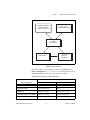


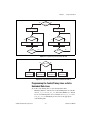

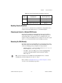


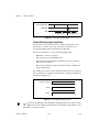

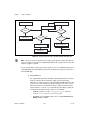
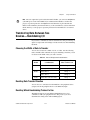


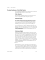

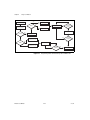

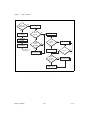

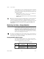
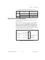


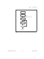

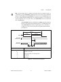
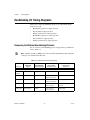
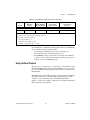

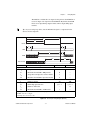


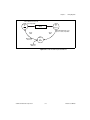
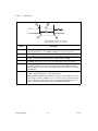
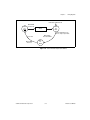
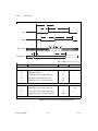
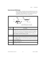
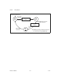


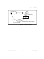

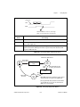
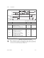
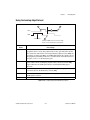

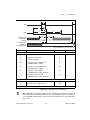
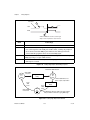
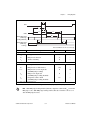


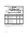
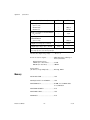

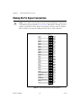
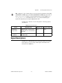
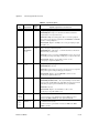

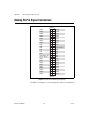
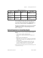
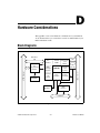


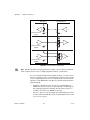

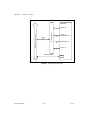

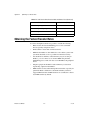


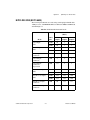
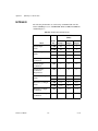
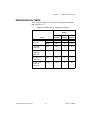
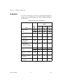
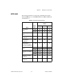
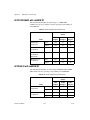
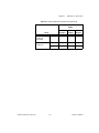


![[Unlocked] SC-2042](http://vs1.manualzilla.com/store/data/005660029_1-1367986a5e7a7fe673239a9957384234-150x150.png)