1
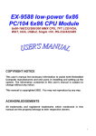
EX-9529 low-power 6x86
3.5” Mini Board
6x86-166/200/233/300 MMX CPU, TFT LCD/VGA, Audio,
100/10M Ethernet, WDT, RS-232/422/485, IrDA, USBx2,
Single +5V, PC/104 socket, DOC, Touch Panel interface,
0~85℃ CPU support 0.8~3.0W low power consumption
COPYRIGHT NOTICE
This user’s manual list necessary information to assist both Embedded
Computer manufacturers and end users in installing and setting up the
system. The information contained in this user’s manual is subject to
change without any notice.
This manual is copyrighted 2002. You may not reproduce by any way.
ACKNOWLEDGEMENTS
All trademarks and registered trademarks which mentioned in this manual
are the property belongs to their respective owners.
1
TABLE OF CONTENTS
CHAPTER 1: INTRODUCTION
1-1
1-2
1-3
ABOUT THIS MANUAL -------------------------------------------------SPECIFICATIONS -------------------------------------------------------SAFETY PRECAUTIONS -----------------------------------------------
6
7
9
CHAPTER 2: HARDWARE CONFIGURATION
2-1
2-2
2-3
2-4
2-5
2-6
2-7
2-8
2-9
2-10
2-11
2-12
2-13
2-14
2-15
2-16
2-17
2-18
2-19
2-20
2-21
2-22
2-23
2-24
2-25
2-26
2-27
2-28
2-29
2-30
2-31
2-32
2-33
2-34
2-36
JUMPERS & CONNECTORS QUICK REFERENCE TABLE -COMPONENTS’ LOCATIONS ----------------------------------------FLOPPY DISK DRIVE CONNECTOR -------------------------------PRINTER CONNECTOR -----------------------------------------------IDE CONNECTOR -------------------------------------------------------COM1 RS-232 CONNECTOR -----------------------------------------COM2 RS-232 CONNECTOR -----------------------------------------IrDA CONNECTOR ------------------------------------------------------4-PIN POWER CONNECTOR ----------------------------------------MINI DIN PS/2 K/B & MOUSE CONNECTOR -------------------VGA CONNECTOR ------------------------------------------------------LCD CONNECTOR ------------------------------------------------------COM2 RS-422/485 CONNECTOR -----------------------------------USB1 CONNECTOR ----------------------------------------------------USB2 CONNECTOR ----------------------------------------------------SUSPEND CONNECTOR (HARDWARE SLEEP) ---------------SYSTEM RESET CONNECTOR -------------------------------------HARD DISK ACTIVE LED & POWER LED -----------------------ETHERNET ACTIVE LED ----------------------------------------------TOUCH PANEL CONNECTOR ---------------------------------------AUDIO OUTPUT CONNECTOR --------------------------------------CD-ROM AUDIO IN CONNECTOR ----------------------------------LCD BACKLIGHT INVERTER POWER CONNECTOR --------M-System ADDRESS SELECT --------------------------------------INTERNAL OR EXTERNAL +12V SELECT-----------------------CMOS BATTERY CLEAR JUMPER --------------------------------WDT OUTPUT SELECT ------------------------------------------------COM2 RS-232/422/485 SELECT ------------------------------------COM2 D-SUB PIN 1,9 VOLTAGE OR SIGNAL SELECT ------LCD PANEL VOLTAGE SELECT -----------------------------------RS-422/485 D-SUB PIN9 VOLTAGE OUTPUT SELECT ------NEGATIVE VOLTAGE INPUT (AT MODE) ------------------------BUZZER --------------------------------------------------------------------144-PIN SO-DIMM SOCKET ------------------------------------------MANUFACTURER DEFAULT JUMPER LIST --------------------
11
12
13
13
14
14
14
15
15
15
15
16
16
16
17
17
17
17
17
17
18
18
18
18
18
18
19
19
19
19
19
19
19
19
20
2
CHAPTER 3: LCD/VGA
3-1
3-2
3-3
PREFACE ------------------------------------------------------------------- 22
UTILITY REFERENCE --------------------------------------------------- 23
QUICK INSTALLATION GUIDE --------------------------------------- 24
CHAPTER 4: 100/10M ETHERNET
4-1
4-2
4-3
INTRODUCTION ---------------------------------------------------------INSTALLATION OF ETHERNET DRIVER ------------------------FURTHER INFORMATION ---------------------------------------------
29
29
33
CHAPTER 5: DiskOnChip FLASH DISK
5-1
5-2
5-3
PREFACE ------------------------------------------------------------------- 35
QUICK INSTALLITION GUIDE ---------------------------------------- 36
UTILITY REFERENCE --------------------------------------------------- 36
CHAPTER 6: WDT
6-1
6-2
WATCHDOG TIMER FUNCTION ------------------------------------WATCHDOG TIMER SOFTWARE GUIDE -------------------------
38
40
CHAPTER 7: AUDIO INSTALLATION
7-1
7-2
INTRODUCTION ---------------------------------------------------------- 42
QUICK INSTALLATION GUIDE --------------------------------------- 42
CHAPTER 8: AWARD BIOS SETUP
8-1
8-2
8-3
8-4
8-5
8-6
8-7
8-8
8-9
MAIN MENU ---------------------------------------------------------------STANDARD CMOS SETUP -------------------------------------------BIOS FEATURES SETUP ---------------------------------------------CHIPSET FEATURES SETUP ---------------------------------------POWER MANAGEMENT SETUP ------------------------------------PNP/PCI CONFIGURATION SETUP --------------------------------INTEGRATED PERIPHERALS ---------------------------------------SUPERVISOR/USER PASSWORD SETTING -------------------BIOS DEFAULT DRIVE TABLE --------------------------------------
46
48
50
53
54
56
58
60
61
APPENDIX A: TECHNICAL SUMMARY
A-1
A-2
A-3
A-4
INTERRUPT MAP --------------------------------------------------------TIMER & DMA CHANNELS MAP ------------------------------------RTC & CMOS RAM MAP -----------------------------------------------I/O & MEMORY MAP ----------------------------------------------------
64
64
65
66
3
APPENDIX B: TROUBLE SHOOTING
B-1
B-2
B-3
TROUBLE SHOOTING POST MESSAGES ------------------------ 68
TROUBLE SHOOTING POST BEEP -------------------------------- 68
TROUBLE SHOOTING POST CODE -------------------------------- 71
4
CHAPTER
INTRODUCTION
THIS CHAPTER SHOWS THE INFORMATION ABOUT CPU CARD AND ITS
SPECIFICATIONS.
SECTIONS INCLUDE:
* ABOUT THIS MANUAL
* SPECIFICATIONS
* SAFETY PRECAUTIONS
5
1-1 ABOUT THIS MANUAL
Thank you for purchasing CPU Card low-power 6x86 3.5” mini-board with
TFT LCD/ VGA interface, Infrared interface, two USB interface, IDE,
100/10M Ethernet, DOC, WDT, audio and optional Touch Panel interface.
This manual is written to assist you to install and set up the system. It
contents six chapters as following:
Chapter 1: INTRODUCTION
This chapter introduces you the background of this manual, and the
specifications for this board. The end in this chapter will indicate how to
avoid the damages for this mini board.
Chapter 2: HARDWARE CONFIGURATION
This chapter outlines the jumpers/connectors/components’ locations
and their functions. It shows the way how to set jumpers and how to
configure this board.
Chapter 3: LCD/VGA
This chapter shows the information about on-board 64-bit LCD/VGA.
It supports CRT and TFT LCD flat panel up to 1280x1024x8 BPP and
1024x768x16 BPP, also support MPEG1 and MPEG2 assist.
Chapter 4: 100/10M Ethernet
This chapter provide the installation and usage guide for network
installers or users.
Chapter 5: DiskOnChip Flash Disk
This chapter brings you the information about DiskOnChip function.
Chapter 6: WDT
Helpful information describes the WatchDog-timer function and its
software guide.
Chapter 7: AWARD BIOS SETUP
This chapter indicates you how to set up the BIOS configurations.
Appendix A: TECHNICAL SUMMARY
This appendix gives you the information about the Award BIOS.
Appendix B: TROUBLE SHOOTING
This appendix outlines the errors and the methods how to ioslate
the problems.
6
1-2 SPECIFICATIONS
* CPU + Chipset:
NS Geode GXLV/GX1 processor & CX5530/A chipset with low-power
6x86-166/200/233/300 MMX CPU built in chip. GXLV support low-power
0~85℃ CPU (1.5W ~ 5.4W), GX1 support very-low-power 0~85℃ CPU
(0.8W ~ 3.0W).
* MEMORY:
1 X 144-pin SO-DIMM socket support 8MB ~ 128MB SDRAM Module.
* CACHE MEMORY: 16KB L1 cache memory.
* I/O Chipset: NS PC97317
* CMOS Backup: CMOS Back up by Li battery.
* BIOS: Award, 128KB Flash BIOS for plug & play function.
* PS/2 KEYBOARD + PS/2 MOUSE:
Support 6-pin Mini-Din PS/2 Keyboard and PS/2 Mouse Connector.
* Touch Panel interface: Optional on board.
* AC97 Audio: Audio codec on board.
* IrDA & USB: Support IrDA x 1, USB x 2.
* BUS TYPE: PC/104 Connector.
* WATCHDOG: Programmable 0 ~ 1024 sec.
* LCD/VGA: On-chip shared-memory 64-bit LCD/VGA, support CRT and TFT
LCD flat panel up to 1280x1024x8 BPP and 1024x768x16 BPP, support
MPEG1 and MPEG2 assist. Using 44-pin LCD Connector.
* 100/10M Ethernet: Realtek 8139C 100/10M Ethernet.
* IDE INTERFACE: Support one port up to 2 x IDE devices.
* DOC FLASH DISK: 32-Pin Socket for DiskOnChip SSD 2MB ~ 288MB.
* Optional IDE FLASH DISK BOARD:
Daughter board support 8/16/32/48/64/96/128/192MB IDE Flash Disk.
7
* FLOPPY DISK DRIVE INTERFACE:
Support up to two Floppy Disk Drives, 3.5” or 5.25” FDD
(360K/720K/1.2M/1.44M/2.88M) Drives A, B swappable.
* SERIAL PORT x 2: 16-byte FIFO 16C550 serial port, jumper selectable
RS- 232 x 1 + RS-232/422/485 x 1.
* PARALLEL PORT:
One bi-directional parallel port configured as LPT1, 2, 3 support IEEE
1284 compliant high-speed EPP and ECP modes.
* Speaker: Buzzer on Board.
* Miscellaneous Connectors/Jumpers:
Reset, HDD LED, single +5V 2-pin power connector and +5V/+12V
4-pin Power connector….
* DMA CONTROLLER: 82C37 X 2
* DMA CHANNELS: 7
* INTERRUPT CONTROLLERS: 82C59 X 2
* INTERRUPT LEVELS: 15
* SYSTEM POWER REQUIREMENT:
+5V/+12V power by using 4-pin HDD power connector, or,
single +5V power by using 2-pin Power connector.
* Operating Temperature: 0℃ to 60℃
0~85℃ CPU support low-power type (1.5W ~ 5.4W), or, optional verylow-power type (0.8W ~ 3W), just need metal cooler (don’t need fan)
* POWER CONSUMPTION: Peak Power
GXLV-233 (2.5V)
GXLV-166 (2.2V)
GX1-300 (2.0V)
GX1-266 (1.8V)
GX1-233 (1.8V)
GX1-200 (1.6V)
5.4W
3.7W
3.0W
2.3W
2.0W
1.6W
Average Power
2.0W
1.0W
1.5W
1.2W
1.0w
0.8W
* BOARD DIMENSION: 145mm x 102mm
* BOARD WEIGHT: 0.20Kg.
8
1-3 SAFETY PRECAUTIONS
Please note the messages below to avoid your system from damage:
1. Avoid your system from static electric power on all occasions.
2. Stay safe from the electric shock. Don’t touch any components of this
card when the power is ON. Always disconnect power when the system is
not in use.
3.Remove power when you change any hardware devices. For instance,
when you connect a jumper or install any cards, a surge of power may
damage the electronic components or the whole system.
9
CHAPTER
HARDWARE CONFIGURATION
THIS CHAPTER SHOWS YOU THE CONNECTORS & JUMPER SETTINGS, AND
COMPONENTS’ LOCATIONS.
SECTIONS INCLUDE:
* CONNECTORS/ JUMPER SETTINGS QUICK REFERENCE TABLE
* COMPONENTS’ LOCATIONS
* CONNECTORS PIN ASSIGNMENTS AND JUMPER SETTINGS
10
2-1 JUMPERS/CONNECTORS QUICK REFERENCE TABLE
FLOPPY DISK DRIVE CONNECTOR …..………………………..
PRINTER CONNECTOR …………........…...............…………….
IDE CONNECTOR ……………………..…..……………………….
COM1 CONNECTOR (RS-232) ……………….…..………………
COM2 RS-232 CONNECTOR ……………..………………………
IrDA CONNECTOR …………….…….……………………………..
4-PIN POWER CONNECTOR ……..………………..…………….
MINI DIN PS/2 K/B & MOUSE CONNECTOR …..…………..….
VGA CONNECTOR ……………....................................………..
LCD CONNECTOR ..……….................................……………...
COM2 RS-422/485 CONNECTOR ..…..………..…………….…..
USB1 CONNECTOR ….…..……..………………….……………..
USB2 CONNECTOR .……..…..…………………….……..………
SUSPEND CONNECTOR (HARDWARE SLEEP) ……………...
SYSTEM RESET SWITCH ……….…..............…………………..
HARD DISK ACTIVE LED & POWER LED ….…….…………....
ETHERNET ACTIVE LED …………………..…………..…………
TOUCH PANEL CONNECTOR ………..…………….……………
AUDIO CONNECTOR ………………….…………………..…..…..
CD-ROM AUDIO IN CONNECTOR .……………………….……..
LCD BACKLIGHT INVERTER POWER CONNECTOR …..……
M-System ADDRESS SELECT ..…………….…………………...
CMOS BATTERY CLEAR JUMPER ………..……………………
WDT OUTPUT SELECTOR ……..………………………………...
COM2 RS-232 OR RS-422/485 SELECTOR …….…………..….
COM2 D-SUB PIN1, 9 VOLTAGE OR SIGNAL SELECT ……...
LCD PANEL VOLTAGE SELECT ………………………………...
RS-422/485 D-SUB PIN9 VOLTAGE OUTPUT SELECT ……...
NEGATIVE VOLTAGE INPUT (AT MODE) ……………………..
BUZZER …………………...…….…………………………………..
144-PIN SO-DIMM SOCKET ……………….……………………..
MANUFACTURE DEFAULT JUMPER LIST …………………….
FDC
LPT
IDE1
COM1
COM2
IR
POWER
KB+MS
VGA
LCD
422/485
USB1
USB2
SUSP
RSTSW
HDLED
LED1
CN1
AUDIO
CDIN
JP1
JP2
JP4
JP5
JP6
JP7
JP8
JP9
JP10
BZ1
DIMM
JP3,JP5
11
2-2 COMPONENTS’ LOCATIONS
HDLED RSTSW
KB/MS CN2 LED1
VGA
COM1
1 1
11
6
1
LCD
6
1
1
+
1
1
1
5
1
COM2
1
BZ1
JP4
SUSP
SLT1
JP3
1
DOC
GXLV(GX1)
POWER
LPT
1
JP5
JP7 JP6
RTL8139C
CX5530
1
LF8200
JP8
USB1
USB2
LDO
1
JP10
1
JP9
1
JP2
1
JP1
CN1
IR 1
1
1
1
IDE1
FDC
CDIN AUDIO
1
1
422/
485
1
1
12
2-3 FLOPPY DISK DRIVE CONNECTOR (FDC)
PIN
1
3
5
7
9
11
13
15
17
19
21
23
25
27
29
31
33
ASSIGNMENT
GND
GND
GND
GND
GND
GND
GND
GND
GND
GND
GND
GND
GND
GND
MID1
GND
MID0
PIN
2
4
6
8
10
12
14
16
18
20
22
24
26
28
30
32
34
ASSIGNMENT
DENSEL
NC
DRATE0
INDEX
MTR0
DRV1
DRV0
MTR1
DIR
STEP
WDATA
WGATE
TRK0
WRTPRT
RDATA
SEL
DSKCHG
2-4 PRINTER CONNECTOR (LPT)
PIN
1
3
5
7
9
11
13
15
17
19
21
23
25
ASSIGNMENT
STROB
PD0
PD1
PD2
PD3
PD4
PD5
PD6
PD7
ACK
BUSY
PE
SLCT
PIN
2
4
6
8
10
12
14
16
18
20
22
24
26
ASSIGNMENT
AUTOFD
ERROR
INIT
SLCTIN
GND
GND
GND
GND
GND
GND
GND
GND
GND
13
2-5 IDE CONNECTOR (IDE1)
PIN
1
3
5
7
9
11
13
15
17
19
21
23
25
27
29
31
33
35
37
39
ASSIGNMENT
RESET
HD7
HD6
HD5
HD4
HD3
HD2
HD1
HD0
GND
DREQ
IOW
IOR
IORDY
DACK
IRQ
SA1
SA0
HDCS0
DASP
PIN
2
4
6
8
10
12
14
16
18
20
22
24
26
28
30
32
34
36
38
40
ASSIGNMENT
GND
HD8
HD9
HD10
HD11
HD12
HD13
HD14
HD15
NC
GND
GND
GND
GND
GND
SINGLE GND
NC
SA2
HDCS1
GND
2-6 COM1 CONNECTOR (RS-232) (COM1)
PIN
1
3
5
7
9
ASSIGNMENT
DCD1
TXD1
GND
RTS1
RI1
PIN
2
4
6
8
ASSIGNMENT
RXD1
DTR1
DSR1
CTS1
2-7 COM2 RS-232 CONNECTOR (COM2)
PIN
1
3
5
7
9
ASSIGNMENT
DCD2
RXD2
TXD2
DTR2
GND
PIN
2
4
6
8
10
ASSIGNMENT
DSR2
RTS2
CTS2
RI2
NC
14
2-8 IrDA CONNECTOR (IR)
PIN
1
3
5
ASSIGNMENT
+5V
IR-RXD
IR-TXD
PIN
2
4
ASSIGNMENT
CIRRXD
GND
2-9 4-PIN POWER CONNECTOR (POWER)
PIN
1
3
ASSIGNMENT
+5V
GND
PIN
2
4
ASSIGNMENT
GND
+12V
2-10 MINI DIN PS/2 K/B & MOUSE CONNECTOR
(KB+MS)
PIN
1
3
5
ASSIGNMENT
KEYBOARD DATA
GND
KEYBOARD CLOCK
PIN
2
4
6
ASSIGNMENT
MOUSE DATA
VCC
MOUSE CLOCK
2-11 VGA CONNECTOR (VGA)
PIN
1
3
5
7
9
11
13
15
ASSIGNMENT
RED
BLUE
GND
GND
VCC
NC
HSYNC
DCSCL
PIN
2
4
6
8
10
12
14
ASSIGNMENT
GREEN
NC
GND
GND
GND
DCSDA
VSYNC
15
2-12 LCD CONNECTOR (LCD)
PIN
1
3
5
7
9
11
13
15
17
19
21
23
25
27
29
31
33
35
37
39
41
43
ASSIGNMENT
+12V
GND
LCDVCC
NC
NC
B0
B2
B4
NC
G0
G2
G4
NC
R0
R2
R4
GND
SHFCLK
M(D.0)
GND
+5V
LCDVCC
PIN
2
4
6
8
10
12
14
16
18
20
22
24
26
28
30
32
34
36
38
40
42
44
ASSIGNMENT
+12V
GND
LCDVCC
GND
NC
B1
B3
B5
NC
G1
G3
G5
NC
R1
R3
R5
GND
VSYNC(FLM)
HSYNC(LP)
ENABKL
+5V
LCDVCC
2-13 COM2 RS-422/485 CONNECTOR (422/485)
PIN
1
3
5
ASSIGNMENT
RXD/TX+
DCD/TXCABLE-RI
PIN
2
4
ASSIGNMENT
DTR/RXTXD/RX+
2-14 USB1 CONNECTOR (USB1)
PIN
1
3
5
ASSIGNMENT
VCC+5V
DB1+
GND
PIN
2
4
ASSIGNMENT
BD1GND
16
2-15 USB2 CONNECTOR (USB2)
PIN
1
3
5
ASSIGNMENT
VCC+5V
DB2+
GND
PIN
2
4
ASSIGNMENT
BD2GND
2-16 HARDWARE SUSPEND CONNECTOR (SUSP)
PIN
1
ASSIGNMENT
SUSP SIGNAL
PIN
2
ASSIGNMENT
GND
2-17 SYSTEM RESET CONNECTOR (RSTSW)
PIN
1
ASSIGNMENT
SIGNAL
PIN
2
ASSIGNMENT
GND
2-18 HARD DISK ACTIVE LED & POWER LED (HDLED)
1-2: Hard Disk Active LED
PIN
1
3
ASSIGNMENT
VCC
VCC
3-4: System Power On LED
PIN
2
4
ASSIGNMENT
SIGNAL
GND
2-19 ETHERNET ACTIVE LED (LED1)
PIN
1
3
5
ASSIGNMENT
VCC
VCC
VCC
PIN
2
4
6
ASSIGNMENT
SIGNAL
SIGNAL
SIGNAL
2-20 TOUCH PANEL CONNECTOR (CN1)
PIN
1
3
ASSIGNMENT
X+
Y+
PIN
2
4
ASSIGNMENT
XY-
17
2-21 AUDIO OUTPUT CONNECTOR (EXTADO)
PIN
1
3
5
7
9
11
13
ASSIGNMENT
LINE IN LEFT
GND
GND
MICHONE IN
LINE OUT LEFT
GND
AMP OUT RIGHT
PIN
2
4
6
8
10
12
14
ASSIGNMENT
GND
LINE IN RIGHT
MICHONE IN
GND
LINE OUT RIGHT
AMP OUT LEFT
GND
2-22 CD-ROM AUDIO IN CONNECTOR (CDIN)
PIN
1
3
ASSIGNMENT
CDL
CDR
PIN
2
4
ASSIGNMENT
GND
GND
2-23 LCD BACKLIGHT INVERTER POWER CONNECTOR
(JP1)
PIN 1: +12V
PIN 2: GND
PIN 3: VCC5V
2-24 M-System ADDRESS SELECT (JP2)
ADDRESS
SELECTION
C000
C800
D000
D800
PIN1&2
ON
OFF
OFF
OFF
JUMPER SETTING
PIN3&4
PIN5&6
OFF
OFF
ON
OFF
OFF
ON
OFF
OFF
PIN7&8
OFF
OFF
OFF
ON
2-25 INTERNAL OR EXTERNAL +12V SELECT (JP3)
1-2 ON: For AT Power +12V (External).
2-3 ON: Use Internal +12V.
2-26 CMOS BATTERY CLEAR JUMPER (JP4)
1-2 ON: NORMAL.
2-3 ON: CMOS CLEAR.
18
2-27 WDT OUTPUT SELECT (JP5)
WatchDog Timer Output for System Reset or IRQ11 Selection.
When JP5 is set to position 1-2 ON, then the output signal of WDT TIMER
will generate a interrupt signal to IRQ11. Once the system accept the
interrupt request, will release a ISR address (CS:E000 IP:0000) for user.
User can write interrupt routine to develop application software.
1-2 ON: IRQ11.
2-3 ON: SYSTEM RESET.
2-28 COM2 RS-232/422/485 SELECT (JP6)
1-2 ON: RS-232 for COM2.
2-3 ON: RS-422/485 for COM2.
2-29 COM2 D-SUB PIN 1, 9 VOLTAGE OR SIGNAL
SELECT (JP7)
1-3 ON: SELECT +12V
2-4 ON: SELECT VCC5V
3-5 ON: SELECT RI2
4-6 ON: SELECT DCD2
2-30 LCD PANEL VOLTAGE SELECT (JP8)
1-2 ON: VCC5V For LCD Panel Voltage.
2-3 ON: VCC3V For LCD Panel Voltage.
2-31 RS-422/485 PIN 9 VOLTAGE SELECTOR (JP9)
1-2 ON: +12V for RS-422/485 connector (COM 2) PIN 9
2-3 ON: +5V for RS-422/485 connector (COM 2) PIN 9
2-32 NEGATIVE VOLTAGE INPUT (AT MODE) (JP10)
PIN
1
3
ASSIGNMENT
GND
GND
PIN
2
4
ASSIGNMENT
-5V
-12V
PIN
2
ASSIGNMENT
SIGNAL
2-33 BUZZER (BZ1)
PIN
1
ASSIGNMENT
VCC
2-34 144-PIN SO-DIMM SOCKET (DIMM)
The CPU CARD mini board use 144-pin SO-DIMM Module.
19
2-35 MANUFACTURER DEFAULT JUMPER LIST
Factory default jumper list as below:
JP3: 2-3 ON
JP5: 1-2 ON
20
CHAPTER
LCD/VGA
This chapter shows the information about LCD/VGA functions.
SECTIONS INCLUDE:
* PREFACE
* UTILITY REFERENCE
* QUICK INSTALLATION GUIDE
21
3-1 PREFACE
CRT Display Modes:
Resolution
Colors
640x480
8 BPP
256 colors
16 BPP
64K colors
RGB
800X600
8 BPP
256 colors
16 BPP
64K colors
RGB
1024X768
1280X1024
8 BPP
256 colors
16 BPP
64K colors
RGB
8 BPP
256 colors
Refresh DOTCLK
Rate (Hz) Rate(Hz)
60
72
75
60
25.175
31.5
31.5
25.175
72
31.5
75
31.5
60
72
75
60
40.0
50.0
49.5
40.0
72
50.0
75
49.5
60
70
75
60
70
75
60
65.0
75.0
78.5
65.0
75.0
78.5
108.0
75
135.0
PCLK
25.175
31.5
31.5
50.35
25.175
63.0
31.5
63.0
31.5
40.0
50.0
49.5
80
40
100
50.0
99
49.5
65.0
75.0
78.5
65.0
75.0
78.5
108.0
54.0
67.5
Graphic Port
Width (Bits)
8
8
8
8
16
8
16
8
16
8
8
8
8
16
8
16
8
16
8
8
8
16
16
16
8
16
16
22
TFT Panel Display Modes
Resolution Simultaneous Refresh DOTCLK PCLK Panel Type
Colors
Rate(MHz) Rate(MHz) (MHz)
640x480
800x600
1024x768
8 BPP
256 colors
60
25.175
25.175
16 BPP
64K colors
RGB
8 BPP
256 colors
60
25.175
25.175
60
40.0
40.0
16 BPP
64 K Colors
60
40.0
40.0
8 BPP
256 colors
60
65
32.5
9-bit
12-bit
18-bit
9-bit
12-bit
18-bit
9-bit
12-bit
18-bit
9-bit
12-bit
18-bit
9-bit/18-I/F
16 BPP
64K colors
60
65
32.5
9-bit/18-I/F
3-2 UTILITY REFERENCE
The CPU Card supports on-chip VGA interface which use shared –
memory technology to share system memory as VGA display buffer.
The CPU CARD delivered with following VGA driver:
-Driver for WIN98
-Driver for WIN95
-Driver for WIN31
-Driver for WIN NT40
-Driver for WIN NT3.51
The driver will put on the diskette or CD. User should install the driver
According the OS. Following shows the example about how to install
the driver.
23
3-3 QUICK INSTALLATION GUIDE
VGA DRIVER FOR WIN95 & 98
A. Install CD Select
D:\3.5Board\EX-9529\vga\Win9x
“National Geode Win9x Drivers1.2.exe”
1
B. Double Click
“National Geode Win9x Drivers 1.2.exe
A. Click “Yes”.
A. Click “Next>”.
24
A. Select “Next >”.
A. Select “Typical” or “Custom” but
the Default is “Typical”.
B. Click “Next >”.
A. Select “ Yes, I want to restart my
computer now”.
B. Click “Finish”.
25
☆ VGA DRIVER FOR NT40
A. Select “Start” Æ”Seting” Æ
”Control Panel”Æ”Display” Æ
”Display Properties”.
B. Click “Display Type”.
A. Click “Change”
A. Click “Have Disk”.
A. Insert CD Select
D:\3.5Board\EX-9529\vga
\nt40\vga
B. Click “OK”.
26
A. You can see “Cyrix Corporation
GX “
B. Click “OK”.
A. Can see “Third-party Drivers”.
B. Click “Yes”.
A. Can see “Installing Driver”.
B. Click “OK”.
C. Restart computer.
27
CHAPTER
100/10M ETHERNET
This chapter shows the information about 100/10M Ethernet functions.
SECTIONS INCLUDE:
* INTRODUCTION
* INSTALLATION OF ETHERNET DRIVER
* FURTHER INFORMATION
28
4-1 INTRODUCTION
The CPU CARD is equipped with a high performance PCI Ethernet chipset
which is fully compliant with IEEE 802.3 100 Mbps CSMA/CD standards. It is
supported by major network operating systems. It is also both 100Base-T and
10Base-T compatible. The medium type can be configured Reltek the
8139C.exe program include on the utility CD. The CPU CARD provides one
10-pin pin header as ethernet connector.
4-2 INSTALLATION OF ETHERNET DRIVER
Before install the Ethernet driver, please note the procedures as below.
You must know which operating system you are using in your CPU
CARD and refer to the corresponding installation flow chart, then follow
the steps described in the flow chart. You will quickly and successfully
complete the installation, even if you are not familiar with instructions
for MS-DOS or Windows.
Note:
The windows illustrations in this chapter are examples
only. You must follow the flow chart instructions and
pay attention to the instructions which then appear on
your screen.
☆ Installation for MS-DOS and Windows 3.1
If you want to set up your Ethernet connection under the MS-DOS or
Windows3.1 environment, you should first check your server system
model. For example, MS-NT or IBM-LAN server, and so on. Then choose
the correct driver to install in your system.
The installation procedures for various servers can be found on CD. The
file path is: D:\>3.5Board\EX-9529\NIC\WFW311
29
☆Installation for Windows 95/98
A. Select “Start” Æ”Setting” Æ
“Control Panel”.
B. Double Click “Add New
Hardware”
A. Can see “Add New Hardware
Wizard”.
B. Click “Next >”.
A. Insert your CD.
B. Select “Browse”
C. d:\ 3.5Board\EX-9529\NIC
\win98
A. Windows driver can show
“Realtek RTL8139(A/B/C/8130)
PCI Fast Ethernet NIC.
B. Click “ Next >”.
30
A. Copying Files.
A. Click “ Finish”.
31
☆Installation for Windows NT
A. Select “Start”, “settings”,
“Control Panel”.
B. Double click “Network”.
A. Choose the “Adapters”
label.
B. Click the “Add” button.
C. Insert CD key-in
D:\ 3.5Board\EX-9529\NIC \
winnt4
A. show Select OEM Option
Realtek RTL8139(A/B/C/8130)
PCI Fast Ethernet Adapter
B. Click “OK”.
32
A. Select RTL8139 Duplex Mode
B. Select “(1) AUTO “
C. Click “ OK “.
A. Can See Microsoft TCP/IP
Properties
B. Key-in “IP Address”
“Subnet Mask”
“Default Gateway”
C. Click “OK”.
A. Network Settings Change.
B. Click “Yes”.
C. Restart your computer now.
4-3 FURTHER INFORMATION
Please reference Realtek website: www.realtek.com.tw
33
CHAPTER
DiskOnChip Flash Disk
THIS CHAPTER
DiskOnChip.
SHOWS
THE
INFORMATION
ABOUT
M-System
SECTIONS INCLUDE:
* PREFACE
* QUICK INSTALLITION GUIDE
* UTILITY REFERENCE
34
5-1 PREFACE
The CPU Card features a DiskOnChip Flash Disk optional function. The
DiskOnChip can be build on board by order. The CPU CARD is designed
to use the DiskOnChip single chip Flash Disk to plug into a standard
32-pin EEPROM socket which built on board. The DiskOnChip Flash Disk
should be mapped into an 8K Byte window in the BIOS expansion
address space of the CPU CARD CPU Card which is usually located
between address 0C0000H to 0EFFFFH. The CPU CARD can contain the
operating system in DiskOnChip to allow systems to boot without a hard
disk.
The DiskOnChip of CPU CARD can install standard MS-DOS and the DOS
can boot from DiskOnChip, its command is fully DOS Command
compatible, such as Del, Deltree, Format, Copy, Xcopy, MD........, users
can read and write DOS Command or data to DiskOnChip same as when
using Hard Disk Drive.
Users can take this DiskOnChip as physical HDD and its priority is
software selectable. For example, if system have one HDD, either HDD &
DiskOnChip could be assigned as C or D Drive. When having two HDD
(Driver C & Driver D), the DiskOnChip could be assigned as C, D, E Drive.
If the system don’t have HDD, the DiskOnChip will be taken as C drive
only. When it is taken as C drive, it can boot system just same as using
Hard Disk Drive.
The capacity of DiskOnChip have 8MB, 12MB, 24MB, 40MB, 72MB,
144MB and 288MB option. User can select the proper one before order to
meet their needs.
The CPU CARD supports M-system DiskOnChip socket which locate at
position ‘DOC’.
35
5-2 QUICK INSTALLITION GUIDE
1.Make sure the CPU Card CPU Card is power OFF
2.Plug the DiskOnChip chip into socket ‘DOC’. Verify the direction is
correct (pin1 of the DiskOnChip is aligned with pin1 of the ‘DOC’
socket).
3.Power ON the system.
4.During power ON you may observe the message displayed by the
DiskOnChip when its driver automatically loaded into system’s
memory.
5.At this stage the DiskOnChip can be accessed as any disk in the
system.
6.If the DiskOnChip is the only disk in the system, it will appear as the
first disk (drive C).
7.If there are more disks besides the DiskOnChip, the DiskOnChip will
appear by default as the last drive.
5-3 UTILITY REFERENCE
If you need more information beside the diskette, please reach the
M-System web www.m-sys.com to get the information.
36
CHAPTER
WDT
THIS CHAPTER SHOWS THE INFORMATION OF WDT FUNCTION, ALSO
DESCRIBES HOW TO INSTALL THE WATCHDOG CONFIGURATION.
SECTIONS INCLUDE:
* WATCHDOG TIMER FUNCTION
* WATCHDOG TIMER SOFTWARE GUIDE
37
6-1 WATCHDOG TIMER FUNCTION
The watchdog timer can reset the system or generate a IRQ11 signal
automatically. It is defined at I/O port 0443H. When you want to enable
the watchdog timer, please write code to I/O port 0443H, then the system
will generate a reset or IRQ11 signal. When you want to disable the
function, write I/O port 043H, the system will stop the WDT function.
The CPU Card watchdog functions: write I/O port address 0443 to enable
watchdog and write I/O port address 043 to disable watchdog.
The following program shows you how to program the watchdog timer in
your program.
WatchDog Enable program:
For Example:
MOV
MOV
OUT
AX, 000FH
DX, 0443H
DX, AX
(choose the values you need; start from 0 to FF )
Watchdog Disable program:
MOV
MOV
OUT
AX, 000FH
DX, 043H
DX, AX
(please ignore this value.)
Please find the time you need and the corresponding value from the
following Watchdog Timer Control Table:
38
TIME BASE IS LIST BELOW
VA Mean is Value for counter
: Unit Hexdecimal
Time Mean is WDT Signal response time : Unit Decimal (second)
Va time Va time va time Va time va time va time va time va time
00 1024 10 64 20 128 30 192 40 256 50 320 60 384 70 448
01
4
11 68 21 132 31 196 41 260 51 324 61 388 71 452
02
8
12 72 22 136 32 200 42 264 52 328 62 392 72 456
03 12 13 76 23 140 33 204 43 268 53 332 63 396 73 460
04 16 14 80 24 144 34 208 44 272 54 336 64 400 74 464
05 20 15 84 25 148 35 212 45 276 55 340 65 404 75 468
06 24 16 88 26 152 36 216 46 280 56 344 66 408 76 472
07 28 17 92 27 156 37 220 47 284 57 348 67 412 77 476
08 32 18 96 28 160 38 224 48 288 58 352 68 416 78 480
09 36 19 100 29 164 39 228 49 292 59 356 69 420 79 484
0a 40 1a 104 2a 168 3a 232 4a 296 5a 360 6a 424 7a 488
0b 44 1b 108 2b 172 3b 236 4b 300 5b 364 6b 428 7b 492
0c 48 1c 112 2c 176 3c 240 4c 304 5c 368 6c 432 7c 496
0d 52 1d 116 2d 180 3d 244 4d 308 5d 372 6d 436 7d 500
0e 56 1e 120 2e 184 3e 248 4e 312 5e 376 6e 440 7e 504
0f
60
1f 124 2f 188 3f 252 4f 316 5f 380 6f 444 7f 508
Va time
80 512
81 516
82 520
83 524
84 528
85 532
86 536
87 540
88 544
89 548
8a 552
8b 556
8c 560
8d 564
8e 568
8f 572
Va time va time Va time va time va time va time va time
90 576 a0 640 b0 704 c0 768 d0 832 e0 896 f0 960
91 580 a1 644 b1 708 c1 772 d1 836 e1 900 f1 964
92 584 a2 648 b2 712 c2 776 d2 840 e2 904 f2 968
93 588 a3 652 b3 716 c3 780 d3 844 e3 908 f3 972
94 592 a4 656 b4 720 c4 784 d4 848 e4 912 f4 976
95 596 a5 660 b5 724 c5 788 d5 852 e5 916 f5 980
96 600 a6 664 b6 728 c6 792 d6 856 e6 920 f6 984
97 604 a7 668 b7 732 c7 796 d7 860 e7 924 f7 988
98 608 a8 672 b8 736 c8 800 d8 864 e8 928 f8 992
99 612 a9 676 b9 740 c9 804 d9 868 e9 932 f9 996
9a 616 aa 680 Ba 744 ca 808 da 872 ea 936 fa 1000
9b 620 ab 684 Bb 748 cb 812 db 876 eb 940 fb 1004
9c 624 ac 688 Bc 752 cc 816 dc 880 ec 944 fc 1008
9d 628 ad 692 Bd 756 cd 820 dd 884 ed 948 fd 1012
9e 632 ae 696 Be 760 ce 824 de 888 ee 952 fe 1016
9f 636 af 700 Bf 764 cf 828 df 892 ef 956 ff 1020
39
6-2 WATCHDOG SOFTWARE GUIDE
User can use WDT function by following way:
1.Direct start WDT function as procedure which described on Sec. 6-1.
FOR EXAMPLE:
MOV AL , 44
OUT 70 , AL
IN
AL , 71
MOV DX , 0443
OUT DX , AL
RET
The above simple software was written under DOS DEBUG. It shows you how
to get the SETUP VALUE from CMOS location 44H.
If you want to read the data correctly, you must put the data 44 value on
register AL first.
Then you must put the register value (44) on port 70H (this mean you need to
addressing the port 70H)
Third you can read one byte data from port 71H
Whenever you need, you can send the data to IO port 0443H to trigger the
WDT timer and for your application.
40
CHAPTER
AUDIO INSTALLATION
THIS CHAPTER SHOWS THE INFORMATION ABOUT AUDIO FUNCTION.
SECTIONS INCLUDE:
* INTRODUCTION
* QUICK INSTALLATION GUIDE
41
7-1 INTRODUCTION
The CPU Card on-board audio interface provides high-quality stereo
sound and FM music synthesis (ESFM) by using the CX5530 audio
controller and Codec chip. The audio interface can record, compress,
and play back voice, sound, and music with a built-in mixer control. The
CPU CARD on-board AC97 audio interface also supports the Plug and
Play (PnP) standard. The ESFM synthesizer is register compatible with
the OPL3 and has extended capabilities.
7-2 QUICK INSTALLATION GUIDE
Before installing the audio driver, please note the detail procedures as
below. You must know which operating system you are using in your
CPU CARD, and then refer to the corresponding installation flow chart
and follow the steps in the flow chart. You can quickly and successfully
complete the installation, even though you are not familiar with
instructions for Windows.
Note: The driver on CD is designated as device “D” through-out
this chapter.
42
☆INSTALLATION FOR WINDOWS 95/98
When you installation “National Geode Win9x Drivers 1.2.exe” Finish.
It’s can auto search audio.
☆INSTALLATION FOR WINDOWS NT
A. Select “Start”, “Settings”,
“Control Panel”.
B. Double click “Multimedia”.
A. Select the “Audio Devices” item.
B. Click “ Add”.
A. Select the “Unlisted Updated
Driver” item.
B. Click “OK”.
43
A. Insert the CD into the CD-ROM
driver
B. Type
“D:\3.5Board\EX-9529\vga\nt40\audi
o”.
C. Click “OK”.
A. Select “XpressAudio [TM] Driver”
B. Click “OK” button.
A. Select I/O Address
B. Click “ Contiune “.
A. Set “Interrupt” “DMA Channel”
“DMA Channel [16-bit]”
“MPU401 I/O Address”
B. Click “OK” .
C. Restart
44
CHAPTER
AWARD BIOS SETUP
THIS CHAPTER SHOWS HOW TO SET UP THE AWARD BIOS.
SECTIONS INCLUDE:
* MAIN MENU
* STANDARD CMOS SETUP
* BIOS FEATURES SETUP
* CHIPSET FEATURES SETUP
* POWER MANAGEMENT SETUP
* PNP/PCI CONFIGURATION SETUP
* INTEGRATED PERIPHERALS
* SUPERVISOR/USER PASSWORD SETTING
* BIOS DEFAULT DRIVE TABLE
45
8-1 MAIN MENU
Once you enter the Award BIOS CMOS Setup Utility, the Main Menu will
appear on the screen. The Main Menu allows you to select from several setup
functions and two exit choices. Use the arrow keys to select among the items
and press <Enter> to accept and enter the sub-menu.
ROM PCI / ISA BIOS (XXXXXXXX)
CMOS SETUP UTILITY
AWARD SOFTWARE, INC.
STANDARD CMOS SETUP
INTEGRATED PERIPHERALS
BIOS FEATURES SETUP
SUPERVISOR PASSWORD
CHIPSET FEATURES SETUP
USER PASSWORD
POWER MANAGEMENT SETUP
IDE HDD AUTO DETECTION
PNP / PCI CONFIGURATION
SAVE & EXIT SETUP
LOAD BIOS DEFAULTS
EXIT WITHOUT SAVING
LOAD SETUP DEFAULTS
Esc : Quit
F10 : Save & Exit Setup
↑↓→← : Select Item
(Shift) F2 : Change Color
Time, Date, Hard Disk Type.....
Note that a brief description of each highlighted selection appears at the
bottom of the screen.
Setup Items:
The main menu includes the following main setup categories. Please note
that some systems may not include all entries.
46
z STANSARD CMOS SETUP
This setup includes all the items in a standard AT-compatible BIOS.
z BIOS FEATURES SETUP
This setup includes all the items of Award special enhanced features.
z CHIPSET FEATURES SETUP
This setup includes all the items of chipset special features.
z POWER MANAGEMENT SETUP
This setup only appears if your system supports Power Management,
“Green PC”, standard.
z PNP / PCI CONFIGYRATION
This setup appears if your system supports PnP / PCI.
z LOAD BIOS DEFAULTS
The BIOS defaults have been set by the manufacturer and represent settings
which provide the minimum requirements for your system to operate.
z LOAD SETUP DEFAULTS
The chipset defaults are settings which provided for maximum system
performance. While Award has designed the custom BIOS to maximize
performance, the manufacturer has the right to change these defaults to meet
their needs.
z INTEGRATED PERIPHERALS
This section includes all the items of IDE hard disk drive and Programmed
Input / Output features. See also Section “Chipset Features Setup”.
z SUPERVISOR / USER PASSWORD SETTING
Change, set, or disable password. It allows you to limit access to the system
and Setup, or just to Setup.
z IDE HDD AUTO DETECTION
Automatically detect and configure hard disk parameters. The Award BIOS
includes this ability in the event you are uncertain of your hard disk’s
parameters. See also Section “Standard CMOS Setup”.
z SAVE & EXIT SETUP
Save CMOS value changes to CMOS and exit setup.
z EXIT WITHOUT SAVE
Abandon all CMOS value changes and exit setup.
47
8-2 STANDARD CMOS SETUP
The items in Standard CMOS Setup Menu are divided into 10 categories.
Each category includes none, one or more than one setup items. Use the
arrow keys to highlight the item and then use the <PgUp> or <PgDn> keys to
select the value you want in each item.
ROM PCI/ISA BIOS (XXXXXXXX)
STANDARD CMOS SETUP
AWARD SOFTWARE, INC.
Date(mm:dd:yy) :
Time(hh:mm:ss):
HARD DISKs
Primary Master
Primary Slave
Secondary Master
Secondary Slave
Drive A
Drive B
Video
Halt On
:
:
:
:
ESC :Quit
F1 :Help
Thu, Mar 23 2000
12 : 30 : 30
TYPE SIZE CYLS HEAD COM LANDS SECTOR
: Auto 0
0
0
0
0
0
: Auto 0
0
0
0
0
0
: Auto 0
0
0
0
0
0
: Auto 0
0
0
0
0
0
1.44 M, 3.5 in.
None
EGA/VGA
All Errors
Base Memory :
Extended Memory :
Other Memory :
Total Memory :
↑↓→←:Select Item
(Shift)F2:Change Color
MODE
Auto
Auto
Auto
Auto
640 K
29184 K
384 K
30208 K
PU / PD / + / - : Modify
z Date
To assign the system date, the format is “mm:dd:yy”. The input range for the
Month is 1-12. Rang for Date is 1-31. Rang for Year is 1994-2079. System BIOS
will calculate the day of the week automatically.
z Time
The time format is <hour> <minute> <second>. The time is calculated based
on the 24-hour military-time clock. For example, 1 p.m. is 13:00:00.
48
z Hard Disks Setting
The BIOS supports Dual-Channel PIO and PCI Bus Master IDE ports. Each
port supports one master and one slave hard drive. You can use <PageUp>
or <PageDown> key to change hard drive type. Incorrect setting may result in
boot up error or system hang. If your hard disk drive is not listed, you can
select Type “USER” to define your own drive manually. We recommend that
you select Type “Auto” for all drives. The BIOS will auto-detect the hard disk
drive and CD-ROM drive at the POST stage. If your hard disk drive is a SCSI
device, please select “None” for your hard drive setting.
z Drive A Type / Drive B Type
The category identifies the types of Floppy Disk Drive A or Drive B that have
been installed in the computer.
z Video
The category selects the type of video adapter used for the primary system
monitor. Although secondary monitors are supported, you do not have to
select the type in Setup.
EGA/VGA
CGA 40
CGA 80
MONO
Enhanced Graphics Adapter/Video Graphics Array. For EGA,
VGA, SEGA, SVGA or PGA monitor adapters.
Color Graphics Adapter, power up in 40 column mode.
Color Graphics Adapter, power up in 80 column mode.
Monochrome adapter include high resolution mono adapters.
z Halt On
This function allows the system to halt when an error is detected during
Power-On Self-Test.
No errors
Whenever the BIOS detects a non-fatal error the system
Would be stopped and you will be prompted.
All errors
The system boot will not be stopped whenever any error
Detected.
All, But Keyboard The system boot will not stop for a keyboard error but
it will stop for all other errors.
All, But Diskette
The system boot will not stop for a disk error but it will
Stop for all other errors.
All, But Disk/Key The system boot will not stop for a keyboard or disk
Error but it will stop for all other errors.
49
8-3 BIOS FEATURES SETUP
This section allows you to configure your system for basic operation. You
can select the system’s default speed, boot-up sequence, shadowing,
keyboard operation and security.
ROM PCI/ ISA BIOS (XXXXXXXX)
BIOS FEATURES SETUP
AWARD SOFTWARE, INC.
Virus Warning
CPU Internal Cache
: Disabled
: Enabled
Quick Power On Self Test
Boot Sequence
Swap Floppy Drive
Boot Up Floppy Seek
Boot Up NumLock Status
Boot Up System Speed
Gate A20 Option
Memory Parity Check
Typematic Rate Setting
Typematic Rate (Chars/Sec)
Typematic Delay (Msec)
Security Option
PCI/VGA Palette Snoop
:
:
:
:
:
:
:
:
:
:
:
:
:
Disabled
A,C,SCSI
Disabled
Disabled
On
High
Fast
Enabled
Disabled
6
250
Setup
Disabled
OS Select For DRAM>64MB : Non-OS2
Report No FDD For WIN 95 : NO
Video BIOS Shadow : Enabled
C8000-CBFFF Shadow : Disabled
CC000-CFFFF Shadow : Disabled
D0000-D3FFF Shadow : Disabled
D4000-D7FFF Shadow : Disabled
D8000-DBFFF Shadow : Disabled
DC000-DFFFF Shadow : Disabled
Cyrix 6x86/MII CPUID : Enabled
ESC:Quit ↑↓→←:Select Item
F1 : Help Pu/Pd/+/-:Modify
F5 : Old Values (Shift)F2 :Color
F6
: Load BIOS Defaults
F7
: Load Setup Defaults
z Virus Warning
When enabled, the BIOS will monitor the boot sector and the partition table
on the hard drive for any attempt to modify. If an attempt is detected, the
BIOS will halt the system and prompt the warning message. Select
“Disabled” if you are installing a new operating system.
z CPU Internal Cache
These two categories speed up memory access. However, it depends on
CPU/ chipset design. The default value is enable.
50
z Quick Power On Self Test
This category speeds up Power On Self Test (POST) after you power up the
computer. If it is set to Enable, BIOS will shorten or skip some check items
during POST.
z Boot Sequence
This option allows user to assign boot sequence of the system. Available
options are A, C, D, E, F, CD-ROM, SCSI and LS120/ZIP.
z Swap Floppy Drive
When enabled, physical drive A will be assigned to logical drive B, and
physical drive B will be assigned to logical drive A.
z Boot Up Floppy Seek
The system will detect and verify operation of the floppy drive type.
z Boot Up NumLock Status
The option allows the <NumLock> key to be activated after system boot up.
z Boot Up System Speed
Selects the default system speed--the normal operating speed at power on.
z Gate A20 Option
This item allows you to select how the gate A20 is handled. The gate A20 is a
device used to address memory above 1 Mbytes. Initially, the gate A20 was
handled via a pin on the keyboard. Today, even keyboards still provide this
support, it is more common and much faster for the system chipset to
provide gate A20 support.
z Memory Parity Check
This item allows you to select memory’s parity check function. The factory
default is Disable (recommended value).
z Typematic Rate Setting
This item determines if the typematic rate is to be used. When disabled,
continually holding down a key on your keyboard will generate only one
instance. In other words, the BIOS will only report that the key is down. When
the typematic rate is enabled, the BIOS will report as before, but it will then
wait a moment, and, if the key is still down, it will begin to report that the key
has been depressed repeatedly. For example, you would use such a feature
to accelerate cursor movements with the arrow keys.
z Typematic Rate (Chars/Sec)
Use this option to set the rate at which a character keeps repeating while you
hold down a key.
51
z Typematic Delay (Msec)
When the typematic rate is enabled, this selection allows you to select the
delay between when the key was first depressed and the acceleration begins.
z Security Option
You can select whether the password is required every time the system boots
or only when you enter the Setup. You can assign “Supervisor Password”
and “User Password” in the main CMOS Setup Utility Screen.
z PCI / VGA Palette Snoop
Enabled this option to correct screen color shifts, when there is a
combination of VGA cards, accelerator cards, or MPEG cards present.
z OS Select for DRAM > 64
If you are using OS/2 operating system and installed memory is larger than
64MB. You need to have the setting in the enable mode.
z Video BIOS Shadow
Video shadow copies BIOS code from slower ROM to faster RAM. BIOS can
then execute from RAM.
z C8000 - CBFFF Shadow/DC000 - DFFFF Shadow
Optional firmware will be copied from ROM to RAM. When this option is
enabled.
52
8-4 CHIPSET FEATURES SETUP
ROM ISA BIOS (XXXXXXXX)
CHIPSET FEATURES SETUP
AWARD SOFTWARE, INC.
SDRAM CAS latency Time : 3T
SDRAM Clock Ratio Div By : 4
16-bit I/O Recovery (CLK)
8-bit I/O Recovery (CLK)
:5
:5
USB Controller
USB Legacy Support
: Enabled
: Enabled
ESC:Quit
↑↓→←:Select Item
F1: Help
Pu/Pd/+/-:Modify
F5: Old Values
(Shift)F2:Color
F6
: Load BIOS Defaults
F7
: Load Setup Defaults
z SDRAM CAS latency Time
These are timing of SDRAM CAS Latency Delay, calculated by clocks.
z SDRAM Clock Ratio Div By
This item can choice SDRAM Clock Ratio. Default is 4.
z 16-bit I/O Recovery (CLK)
This option specifies the length of a delay inserted between consecutive
16-bit I/O operations.
z 8-bit I/O Recovery (CLK)
This option specifies the length of a delay inserted between consecutive 8-bit
I/O operations.
53
8-5 POWER MANAGEMENT SETUP
ROM PCI/ISA BIOS (XXXXXXXX)
POWER MANAGEMENT SETUP
AWARD SOFTWARE, INC.
Power Management :
User Define IRQ1 (KeyBoard)
IRQ3 (COM 2)
IRQ4 (COM 1)
∗∗ PM Timers ∗∗
Doze Mode
:Disabled IRQ5 (LPT 2)
Standby Mode
:Disabled IRQ6 (Floppy Disk)
HDD Power Down
:Disabled IRQ7 (LPT 1)
MODEM Use IRQ
:NA
IRQ9 (IRQ2 Redir)
IRQ10 (Reserved)
Throttle Duty Cycle
:33.3 %
IRQ11 (Reserved)
IRQ12 (PS/2 Mouse)
IRQ13 (Coprocessor)
IRQ14 (Hard Disk)
IRQ15 (Reserved)
: ON
: OFF
: OFF
: OFF
: OFF
: OFF
: OFF
: OFF
: OFF
: ON
: OFF
: OFF
: OFF
ESC:Quit ↑↓→←:Select Item
F1: Help Pu/Pd/+/-:Modify
F5 : Old Values (Shift)F2 : Color
F6 : Load BIOS Defaults
F7 : Load Setup Defaults
z Power Management
This item allows you to select the type (or degree) of power saving and it is
directly related to the following modes:
There are three selections for Power management, four of which have fixed
mode settings.
Disabled
The system operates in Normal conditions (Non-GREEN), and
the Power Management function is disabled.
Max. saving This mode will maximize the power saving capability.
Min. saving This mode will minimize the power saving capability.
User define Allow user to define time-out parameters to control power
saving. Refer item shown below.
54
z PM Timers
The following four modes are Green PC power saving functions which are
only user configurable when User Defined Power Management has been
selected. See above for available selections.
1. Doze Mode
When system is inactive after the predefined time limit, system performance
will drop down. This is the first level of Power Management.
2. Standby Mode
System turns off the video signal and the fixed drives. This is the second
level of Power Management.
3. HDD Power Down
This instructs hard drives to shut off while in the Power Management modes.
4. MODEM Use IRQ
This item tells the Power Management BIOS which IRQ is assigned to the
installed MODEM. Option are NA, 3, 4,5,7, 9,10, and 11.
z Power Down & Resume Events
Power Down and Resume events are I/O events whose occurrence can
prevent the system from entering a power saving mode or can awaken the
system from such a mode. In fact, the system remains alert for anything
occurs to a device which is configured as ON, even when the system is in a
Power Down mode. The following is a list of IRQ’s, Interrupt Requests, which
can be exempted as much as the above COM ports and LPT ports can. When
an I/O device wants to gain the attention of the operating system, it activate
this by causing an IRQ to occur. When the operating system respond to the
request, it interrupts itself and performs the service. The choices are ON and
OFF (Default). When set to ON, activity will neither prevent the system from
going into a power management mode nor awaken it.
* IRQ3 (COM2)
* IRQ6 (Floppy Disk)
* IRQ9 (IRQ2 Redir)
* IRQ12 (PS/2 Mouse)
* IRQ15 (Reserved)
* IRQ4 (COM1)
* IRQ5 (LPT 2)
* IRQ7 (LPT 1)
* IRQ8 (RTC Alarm)
* IRQ10 (Reserve)
* IRQ11 (Reserved)
* IRQ13 (Coprocessor) * IRQ14 (Hard Disk)
55
8-6 PNP/PCI CONFIGURATION SETUP
This section describes about configuring the PCI bus system. PCI (Personal
Computer Interconnect) is a bus standard which allows I/O devices to
operate at the speed near to the speed which is the CPU itself uses when
communicating with its own special components. This section covers some
very technical item and it is strongly recommended that only experienced
users should make any changes to the default settings.
ROM PCI/ISA BIOS (XXXXXXXX)
PNP/PCI CONFIGURATION
AWARD SOFTWARE, INC.
PNP OS Installed
Resources Controlled By
Reset Configuration Data
: NO
: Auto
: Disabled
PCI IRQ Actived By
: Level
ESC:Quit
↑↓→←:Select Item
F1: Help
Pu/Pd/+/-:Modify
F5
: Old Values (Shift)F2:Color
F6
: Load BIOS Defaults
F7
: Load Setup Defaults
56
z PNP OS Installed
This Field allows you to use a Plug-and-Play (PnP) operating system. Please
set it as “ No” if the operating system has no PnP function or to avoid
reassigning the IRQs by the operating system.
z Resources Controlled By
Default setting is “ Auto”. This setting allows the BIOS to self detect setting
and Plug-and-Play devices during start up. The user can select and configure
IRQs under “Manual” mode.
z Reset Configuration Data
In case a conflict occurs after you assign the IRQs or after you configure you
system, you can enable this function to allow your system to automatically
reset your configuration and reassign the IRQs, DMAs, and I/O address.
z IRQ-XX assigned to
If your ISA card is not PnP compatible and requires a special IRQ to support
its function, set the select IRQ-x assigned to : “Legacy ISA”. This setting
informs the PnP BIOS to reserve the selected IRQ for the installed legacy ISA
card.
z DMA-X assigned to
If your ISA card is not PnP compatible and requires a special DMA channel to
support its function, set the select DMA channel to : “Legacy ISA”. This
setting informs the PnP BIOS to reserve the selected DMA channel for the
installed legacy ISA card.
57
8-7 INTEGRATED PERIPHERALS
ROM PCI/ISA BIOS (XXXXXXXX)
CMOS SETUP UTILITY
AWARD SOFTWARE, INC.
IDE HDD Block Mode
Primary IDE Channel
Master Drive PIO Mode
Slave Driver PIO Mode
Secondary IDE Channel
Master Drive PIO Mode
Slave Driver PIO Mode
:
:
:
:
:
Disabled ECP Mode Use DMA
Enabled
Auto
Build in CPU Audio
Auto
Enabled
Auto
Auto
IDE Primary Master UDMA :
IDE Primary Slave UDMA :
IDE Secondary Master UDM
IDE Secondary Slave UDMA :
Auto
Auto
Auto
Auto
KBC input clock
Onboard FDC Controller
Onboard Serial Port 1
Onboard Serial Port 2
UR2 Mode
Onboard Parallel Port
Parallel Port Mode
8 MHz
Enabled
3F8/IRQ4
2F8/IRQ3
Standard
378/IRQ7
Normal
:
:
:
:
:
:
:
: 3
: Disabled
Multiple Monitor Support : Onboard
Video Memory Size
: 2.5 M
Flat Panel Status
: Enabled
Flat Panel Resolution
: 800x600
ESC:Quit ↑↓→←:Select Item
F1: Help
Pu/Pd/+/- : Modify
F5: Old Values (Shift)F2 : Color
F6: Load BIOS Defaults
F7: Load Setup Defaults
NOTE: If you don’t use the on-board IDE connector, then use on-card
(ISA Card) IDE connector. You will set Onboard Primary IDE:
Disabled an Onboard Secondary IDE: Disabled from CHIPSET
FEATURES SETUP UTILITY.
58
z IDE HDD Block Mode
This feature enhances disk performance by allowing multi-sector data
transfers and eliminates the interrupt handling time for each sector.
z IDE Primary Master & Secondary Master/Slave PIO:
These four PIO fields let you set a PIO mode (0-4) for each of four IDE
devices. When under “Auto” mode, the system automatically set the best
mode for each device.
z IDE Primary Master & Secondary Master/Slave UDMA:
When set to “ Auto” mode, the system will detect if the hard drive supports
Ultra DMA mode.
z Onboard FDC Controller:
Select “Enabled” to activate the on-board FDC
Select “Disabled” to activate an add-on FDC
z Onboard Serial Port 1 & 2
Select an address and corresponding interrupt for the first/second serial
port. The default value for the first serial port is “3F8/IRQ4” and the second
serial port is “2F8/IRQ3”.
z UR2 Mode
Select to activate the Infrared transfer function.
z Onboard Parallel port:
Select address and interrupt for the Parallel port.
z Parallel Port Mode:
Select an operating mode for the parallel port. Mode options are SPP, EPP1.7,
EPP1.9, ECP and ECP/EPP1.7, ECP/EPP1.9 .
z Video Memory Size:
This item is setting Video Memory Size.
z Flat Panel Status: This item is setting LCD Enabled or Disabled.
z Flat Panel Resolution:
This item is setting LCD Resolution “640x480, 800x600, 1024x768”
59
8-8 SUPERVISOR/USER PASSWORD SETTING
You can set either supervisor or user password, or both of them. The
difference between them are: ‘supervisor password’ can enter and change
the options of the setup menus and ‘user password’ just can enter but do not
have the right to change the options of the setup menus.
When you select this function, the following message will appear at the
center of the screen to assist you in creating a password.
ENTER PASSWORD :
Type the password, up to eight characters in length, and press <Enter>. The
password typed now will clear any previously entered password from CMOS
memory. You will be asked to confirm the password. Type the password
again and press <Enter>. You may also press <Esc> to abort the selection
and not enter a password.
To disable a password, just press <Enter> when you are prompted to enter
the password. A message will confirm the password will be disabled. Once
the password is disabled, the system will boot and you can enter Setup
freely.
PASSWORD DISABLED.
When a password has been enabled, you will be prompted to enter it every
time you try to enter Setup. This prevents an unauthorized person from
changing any part of your system configuration.
Additionally, when a password is enabled, you can also require the BIOS to
request a password every time your system is rebooted. This would prevent
unauthorized use of your computer.
You determine when the password is required within the BIOS Features
Setup Menu and its Security option. If the Security option is set to “System”,
the password will be required both at boot and at entry to Setup. If set to
“Setup”, prompting only occurs when trying to enter Setup.
60
8-9 BIOS DEFAULT DRIVE TABLE
This is the current list of the drive type table contained in Setup.
Type Size Cylinder Hea Sectors Write Land Example Model
(MB)
s
ds
Preco Zone
mp
1
10
306
4
17
128
305 TEAC SD510, MMI 112,
5412
2
21
615
4
17
300
615 Seagate ST225, ST4026
3
32
615
6
17
300
615
4
65
940
8
17
512
940
5
49
940
6
17
512
940
6
21
615
4
17
65535 615 Seagate ST125, Tandon
TM262
7
32
462
8
17
256
511
8
31
733
5
17
65535 733 Tandon TM 703
9
117
900
15
17
65535 901
10
21
820
3
17
65535 820
11
37
855
5
17
65535 855
12
52
855
7
17
65535 855
13
21
306
8
17
128
319 Disctron 526, MMI M125
14
44
733
7
17
65535 733
15
Reserve
d
Microscience HH725,
16
21
612
4
17
0
663 Syquest 3250,3425
17
42
977
5
17
300
977
18
59
977
7
17
65535 977
19
62
1024
7
17
512 1023
20
31
733
5
17
300
732
21
44
733
7
17
300
732
22
31
733
5
17
300
733 Seagate ST4038
23
10
306
4
17
0
336
24
42
977
5
17
65535 976 Seagate ST4051
25
80
1024
9
17
65535 1023 Seagate ST4096
26
74
1224
7
17
65535 1223 Maxtor 2085
27
117
1224
11
17
65535 1223 Maxtor 2140, Priam S14
28
159
1224
15
17
65535 1223 Maxtor 2190, Priam S19
29
71
1024
8
17
65535 1023 Maxtor 1085, Micropolis
1325
61
30
31
32
33
34
35
36
37
38
39
40
41
98
87
72
89
106
115
124
17
142
119
42
44
1024
918
925
1024
1024
1024
1024
1024
1024
918
820
1024
11
11
9
10
12
13
14
2
16
15
6
5
17
17
17
17
17
17
17
17
17
17
17
17
65535
65535
65535
65535
65535
65535
65535
65535
65535
65535
65535
65535
1023
1023
926
1023
1023
1023
1023
1023
1023
1023
820
1023
42
43
44
45
User
68
42
64
104
1024
809
809
776
5
6
6
8
26
17
26
33
65535
65535
65535
65535
1023
852
852
775
Maxtor 1105, 1120, 4780
Maxtor 1170
CDC 9415
Maxtor 1140, 4380
Seagate ST251
Seagate 4053
Miniscribe3053/6053
Miniscribe 3053/ 6053 RLL
Miniscribe 3650
Miniscribe 3675 RLL
Conner CP3104
62
APPENDIX
TECHNICAL SUMMARY
THIS SECTION SHOWS YOU THE MAPS CONCISELY.
SECTIONS INCLUDE:
* INTERRUPT MAP
* TIMER & DMA CHANNELS MAP
* RTC & CMOS RAM MAP
* I/O & MEMORY MAP
63
A-1 INTERRUPT MAP
IRQ
0
1
2
3
4
5
6
7
8
9
10
11
12
13
14
15
ASSIGNMENT
System TIMER interrupt from TIMER-0
Keyboard output buffer full
Cascade for IRQ 8-15
Serial port 2
Serial port 1
Parallel port 2
Floppy Disk adapter
Parallel port 1
RTC clock
Available
Available
Available
Available
Math coprocessor
Hard Disk adapter
Available
A-2 TIMER & DMA CHANNELS MAP
z Timer Channel Map
Timer Channel Assignment
0
System timer interrupt
1
DRAM Refresh request
2
Speaker tone generator
z DMA Channel Map
DMA Channel Assignment
0
Available
1
IBM SDLC
2
Floppy Disk adapter
3
Channel-3 Available
4
Cascade for DMA controller 1
5
Available
6
Available
7
Available
64
A-3 RTC & CMOS RAM MAP
CODE
00
01
02
03
04
05
06
07
08
09
0A
0B
0C
0D
0E
0F
10
11
12
13
14
15
16
17
18
30
31
32
33
34-3F
40-7F
ASSIGNMENT
Seconds
Second alarm
Minutes
Minutes alarm
Hours
Hours alarm
Day of week
Day of month
Month
Year
Status register A
Status register B
Status register C
Status register D
Diagnostic status byte
Shutdown byte
Floppy Disk drive type byte
Reserve
Hard Disk type byte
Reserve
Equipment byte
Base memory low byte
Base memory high byte
Extension memory low byte
Extension memory high byte
Reserved for extension memory low byte
Reserved for extension memory high byte
Date Century byte
Information Flag
Reserve
Reserved for Chipset Setting Data
65
A-4 I/O & MEMORY MAP
z Memory Map
MEMORY MAP
0000000-009FFFF
00A0000-00BFFFF
00C0000-00DFFFF
ASSIGNMENT
System memory used by DOS and application
Display buffer memory for VGA/EGA/CGA/MONO
Adapter
Reserved for I/O device BIOS ROM or RAM buffer.
00E0000-00EFFFF
00F0000-00FFFFF
0100000-BFFFFF
Reserved for PCI device ROM
System BIOS ROM
System extension memory
z I/O Map
I/O MAP
000-01F
020-021
022-023
040-05F
060-06F
070-07F
080-09F
0A0-0BF
0C0-0DF
0F0-0FF
1F0-1F8
278-27F
2B0-2DF
2F8-2FF
360-36F
378-37F
3B0-3BF
3C0-3CF
3D0-3DF
3F0-3F7
3F8-3FF
ASSIGNMENT
DMA controller (Master)
Interrupt controller (Master)
Chipset controller registers I/O ports.
Timer control registers.
Keyboard interface controller (8042)
RTC ports & CMOS I/O ports
DMA register
Interrupt controller (Slave)
DMA controller (Slave)
Math coprocessor
Hard Disk controller
Parallel port-2
Graphics adapter controller
Serial port-2
Net work ports
Parallel port-1
Monochrome & Printer adapter
EGA adapter
CGA adapter
Floppy disk controller
Serial port-1
66
APPENDIX
TROUBLE
SHOOTING
THIS SECTION SHOWS THE ERRORS MAY OCCUR WHEN YOU OPERATE
THE SYSTEM, ALSO GIVE YOU THE SUGGESTIONS ON SOLVING THE
PROBLEMS.
SECTIONS INCLUDE:
* TROUBLE SHOOTING POST MESSAGE
* TROUBLE SHOOTING POST BEEP
* TROUBLE SHOOTING FOR POST CODES
67
B-1 TROUBLE SHOOTING POST MESSAGES
During the Power On Self Test (POST), if the BIOS detects an error requiring
you to do something to fix, it will either sound a beep code or display a
message. If a message is displayed, it will be accompanied by:
PRESS F1 TO CONTINUE, CTRL-ALT-ESC OR DEL TO ENTER SETUP
B-2 TROUBLE SHOOTING POST BEEP
Currently there are two kind of beep codes in BIOS.
The one code indicates that a video error has occurred and the BIOS cannot
initialize the video screen to display any additional information. This beep
code consists of a single long beep followed by three short beeps. The other
code indicates that your DRAM error has occurred. This beep code consists
of a single long beep repeatedly.
z Error Messages
One or more error messages may be displayed if the BIOS detects an error
during the POST. This list includes messages for both the ISA and the EISA
BIOS.
z CMOS BATTERY HAS FAILED
CMOS battery is no longer functional. It should be replaced.
z CMOS CHECKSUM ERROR
Checksum of CMOS is incorrect. This can indicate that CMOS has become
corrupt. This error may have been caused by a weak battery. Check the
battery and replace if necessary.
z DISK BOOT FAILURE, INSERT SYSTEM DISK AND PRESS
ENTER
No boot device was found. This could mean that either a boot drive was not
detected or the drive does not contain proper system boot files. Insert a
system disk into Drive A: and press <Enter>. If you assumed the system
would boot from the hard drive, make sure the controller is inserted correctly
and all cables are properly attached. Also be sure that the disk is formatted
as a boot device. Then reboot the system.
z DISKETTE DRIVES OR TYPES MISMATCH ERROR - RUN SETUP
Type of diskette drive installed in the system is different from the CMOS
definition. Run Setup to reconfigure the drive type correctly.
68
z DISPLAY SWITCH IS SET INCORRECTLY
Display switch on the motherboard can be set to either monochrome or color.
This indicates the switch is set to a different setting than indicated in Setup.
Determine which setting is correct, and then turn off the selection.
z DISPLAY TYPE HAS CHANGED SINCE LAST BOOT
Since last power off the system, the display adapter has been changed. You
must configure the system for the new display type.
z ERROR ENCOUNTERED INITIALIZING HARD DRIVE
Hard drive cannot be initialized. Be sure the adapter is installed correctly and
all cables are correctly and firmly attached. Also be sure the correct hard
drive type is selected in Setup.
z ERROR INITIALIZING HARD DISK CONTROLLER
Cannot initialize controller. Make sure the card is correctly and firmly
installed in the bus. Be sure the correct hard drive type is selected in Setup.
Also check if any jumper needs to be set correctly on the hard drive.
z FLOPPY DISK CNTRLR ERROR OR NO CNTRLR PRESENT
Cannot find or initialize the floppy drive controller. Make sure the controller is
installed correctly and firmly. If there are no floppy drives installed, be sure
the Diskette Drive selection in Setup is set to NONE.
z Invalid EISA Configuration
PLEASE RUN EISA CONFIGURATION UTILITY. The non-volatile memory
containing EISA configuration information was programmed incorrectly or
has become corrupt. Re-run EISA configuration utility to correctly program
the memory.
NOTE: When this error appears, the system will boot in ISA mode, which
allows you to run the EISA Configuration Utility.
z KEYBOARD ERROR OR NO KEYBOARD PRESENT
Cannot initialize the keyboard. Make sure the keyboard is attached correctly
and no keys are being pressed during the boot. If you are purposely
configure the system without a keyboard, set the error halt condition in Setup
to HALT ON ALL, BUT KEYBOARD. This will cause the BIOS to ignore the
missing keyboard and continue the boot.
z MEMORY ADDRESS ERROR AT ...
Indicates a memory address error at a specific location. You can use this
location along with the memory map for your system to find and replace the
bad memory chips.
69
z MEMORY PARITY ERROR AT ...
Indicates a memory parity error at a specific location. You can use this
location along with the memory map for your system to find and replace the
bad memory chips.
z MEMORY SIZE HAS CHANGED SINCE LAST BOOT
Memory has been added or removed since the last boot. In EISA mode, use
Configuration Utility to reconfigure the memory configuration. In ISA mode,
enter Setup and enter the new memory size in the memory fields.
z MEMORY VERIFY ERROR AT ...
Indicates an error verifying a value already written to memory. Use the
location along with your system’s memory map to locate the bad chip.
z OFFENDING ADDRESS NOT FOUND
This message is used in conjunction with the I/O CHANNEL CHECK and RAM
PARITY ERROR messages when the segment that has caused the problem
which cannot be isolated.
z OFFENDING SEGMENT:
This message is used in conjunction with the I/O CHANNEL CHECK and RAM
PARITY ERROR messages when the segment that has caused the problem
which has been isolated.
z PRESS A KEY TO REBOOT
This will be displayed at the bottom screen when an error occurs that
requires you to reboot. Press any key and the system will reboot.
z PRESS F1 TO DISABLE NMI, F2 TO REBOOT
When BIOS detects a Non-maskable Interrupt condition during boot, this will
allow you to disable the NMI and continue to boot, or you can reboot the
system with the NMI enabled.
z RAM PARITY ERROR - CHECKING FOR SEGMENT ...
Indicates a parity error in Random Access Memory.
z SYSTEM HALTED, (CTRL-ALT-DEL) TO REBOOT ...
Indicates the present boot attempt has been aborted and the system must be
rebooted. Press and hold down the CTRL and ALT keys and press DEL.
70
B-3 TROUBLE SHOOTING FOR POST CODES
NOTE: EISA POST codes are typically output to port address 300h.
ISA POST codes are output to port address 80h.
POST Name
Description
(hex)
C0 Turn Off Chipset Cache OEM Specific - Cache control
1
Processor Test 1
Processor Status (1 FLAG) Verification.
Tests the following processor status flags
carry, zero, sign, overflow. The BIOS will set
each of these flags, verify they are set, then
turn each flag off and verify it is off.
2
Processor Test 2
Read/Write/Verify all CPU registers except
SS, SP, and BP with data pattern FF and 00.
3
Initialize Chips
Disable NMI, PIE, AIE, UEI, SQWV. Disable
video, parity checking, DMA. Reset math
coprocessor. Clear all page registers,
CMOS shutdown byte. Initialize timer 0, 1,
and 2, including set EISA timer to a known
state.
Initialize DMA controllers 0 and 1.
Initialize interrupt controllers 0 and 1.
Initialize EISA extended registers.
4
Test Memory Refresh
RAM must be periodically refreshed in order
to keep the memory from decaying. This
Toggle
function assures that the memory refresh
function is working properly.
5
Blank video,
Keyboard controller initialization.
Initialize keyboard
6
Reserved
7
Test CMOS Interface
Verifies CMOS is working correctly, detects
And Battery Status
bad battery.
BE Chipset Default
Program chipset registers with power on
Initialization
BIOS defaults.
C1 Memory presence test OEM Specific-Test to size on-board memory
C5 Early Shadow
OEM Specific – Early Shadow enable for fast
boot.
C6 Cache presence test
External cache size detection
8
Setup low memory
Early chipset initialization
Memory presence test
OEM chipset routines
71
Clear low 64K of memory
Test first 64K memory.
9
Early Cache
Cyrix CPU initialization
Initialization
Cache initialization
A
Setup Interrupt Vector Initialize first 120 interrupt vectors with
Table
SPURIOUS_INT_HDLR and initialize INT
00h-1Fh according to INT_TBL
B
Test CMOS RAM
Test CMOS RAM Checksum, if bad, or
Checksum
insert key pressed, load defaults.
C
Initialize keyboard
Detect type of keyboard controller
(optional) Set NUM_LOCK status.
D
Initialize Video Interface Detect CPU clock. Read CMOS location
14h to find out type of video in use.
Detect and Initialize Video Adapter.
E
Test Video Memory
Test video memory, write sign-on message
to screen. Setup shadow RAM - Enable
shadow according to Setup.
F
Test DMA Controller 0
BIOS checksum test. Keyboard detect and
initialization.
10 Test DMA Controller 1
11 Test DMA Page
Test DMA Page Registers.
Registers
12-13 Reserved
14 Test Timer Counter 2
Test 8254 Timer 0 Counter 2.
15 Test 8259-1 Mask Bits
Verify 8259 Channel 1 masked interrupts by
alternately turning off and on the interrupt
lines.
16 Test 8259-2 Mask Bits
Verify 8259 Channel 2 masked interrupts by
alternately turning off and on the interrupt
lines.
17 Test Stuck 8259’s
Turn off interrupts then verify no interrupt
Interrupt Bits
mask register is on.
18 Test 8259 Interrupt
Force an interrupt and verify the interrupt
Functionality
occurred.
19 Test Stuck NMI Bits
Verify NMI can be cleared.
(Parity I/O Check)
1A
Display CPU clock.
1B-1E Reserved
1F Set EISA Mode
If EISA non-volatile memory checksum is
correct, execute EISA initialization. If not,
execute ISA tests an clear EISA mode flag.
Test EISA Configuration Memory Integrity
(checksum & communication interface).
72
20 Enable Slot 0
21-2F Enable Slots 1-15
30 Size Base and Extended
Memory
31 Test Base and Extended
Memory
32
Test EISA Extended
Memory
33-3B Reserved
3C Setup Enabled
3D Initialize & Install
Mouse
3E Setup Cache Controller
3F Reserved
BF Chipset Initialization
Initialize slot 0 (System Board).
Initialize slots 1 through 15.
Size base memory from 256K to 640K and
extended memory above 1MB.
Test base memory from 256K to 640K and
extended memory above 1MB by using
various patterns.
NOTE: This will be skipped in EISA mode
and can be “skipped” with ESC key in ISA
mode.
If EISA Mode flag is set then test EISA
memory found in slots initialization.
NOTE: This will be skipped in ISA mode and
can be “skipped” with ESC key in EISA
mode.
Detect if mouse is present, initialize mouse,
install interrupt vectors.
Initialize cache controller.
Program chipset registers with Setup
Values
40
Display virus protect disable or enable
41 Initialize Floppy Drive & Initialize floppy disk drive controller and
Controller
any drives.
42 Initialize Hard Drive &
Initialize hard drive controller and any
Controller
drives.
43 Detect & Initialize
Initialize any serial and parallel ports (also
Serial/Parallel Ports
game port).
44 Reserved
45 Detect & Initialize math Initialize math coprocessor.
Coprocessor
46 Reserved
47 Reserved
48-4D Reserved
4E Manufacturing POST
Reboot if Manufacturing POST Loop pin is
Loop or Display
set. Otherwise display any messages (i.e.,
Messages
any non-fatal errors that were detected
during POST) and enter Setup.
4F Security Check
Ask password security (optional).
50 Write CMOS
Write all CMOS values back to RAM and
73
51
Pre-boot Enable
52
Initialize Option ROMs
53
60
61
62
63
B0
B1
Initialize Time Value
Setup Virus Protect
Set Boot Speed
Setup NumLock
Boot Attempt
Spurious
Unclaimed NMI
E1-EF Setup Pages
FF Boot
clear screen.
Enable parity checker. Enable NMI, Enable
cache before boot.
Initialize any option ROMs present from
C8000h to EFFFFh.
NOTE: When FSCAN option is enabled, will
initialize from C8000h to F7FFFh.
Initialize time value in 40h: BIOS area.
Setup virus protect according to Setup.
Set system speed for boot.
Setup NumLock status according to Setup.
Set low stack. Boot via INT 19h.
If interrupt occurs in protected mode.
If unmasked NMI occurs, display. Press F1
to disable NMI, F2 reboot.
E1 - Page 1, E2 – Page 2, etc.
74