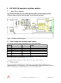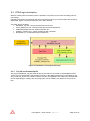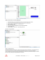
1
PA72 series User Manual Revision 1.10 February 2015 APPLICOS bv, Veldkampseweg 1, 8181LN, Heerde, The Netherlands Table of Contents Table of Contents .......................................................................................................... 2 1 Terminology ............................................................................................................ 5 2 Introduction ............................................................................................................. 6 3 PA72 Base board .................................................................................................... 7 3.1 Base board block diagram ........................................................................................................ 7 3.2 Clock sources ........................................................................................................................... 8 3.3 Trigger ...................................................................................................................................... 9 3.3.1 Trigger timing................................................................................................................... 10 3.4 Calibration ADC ...................................................................................................................... 10 3.4.1 Module calibration ........................................................................................................... 11 3.5 4 5 6 7 8 Front panel channel LEDs ...................................................................................................... 11 General module memory structure and signal definition ................................. 12 4.1 Module Operational modes .................................................................................................... 12 4.2 Module Stimulus memory architecture ................................................................................... 12 4.3 Module Capture memory architecture .................................................................................... 13 4.4 Stimulus signal definition ........................................................................................................ 14 PA72G16400 waveform generator module ......................................................... 18 5.1 Board block diagram ............................................................................................................... 18 5.2 Output voltage and available signal ranges ........................................................................... 18 5.3 DC-Offset ................................................................................................................................ 18 5.4 Filter section ........................................................................................................................... 19 5.5 Clocks, trigger and stimulus ................................................................................................... 19 5.6 Memory ................................................................................................................................... 20 PA72D16180A Waveform digitizer module......................................................... 21 6.1 Board block diagram ............................................................................................................... 21 6.2 Input ranges and common-mode ranges................................................................................ 21 6.3 Filter section ........................................................................................................................... 22 6.4 Input connection configuration ................................................................................................ 23 6.5 DC-Offset source .................................................................................................................... 23 6.6 Clocks and trigger ................................................................................................................... 24 6.7 Memory ................................................................................................................................... 24 6.8 Module auto calibration .......................................................................................................... 25 PA72G14180 waveform generator module ......................................................... 26 7.1 Board block diagram ............................................................................................................... 26 7.2 Output voltage and available signal ranges ........................................................................... 26 7.3 DC offset ................................................................................................................................. 26 7.4 Filter section ........................................................................................................................... 27 7.5 Clocks, trigger and stimulus ................................................................................................... 27 PA72D14130 waveform digitizer module ............................................................ 29 8.1 Board block diagram ............................................................................................................... 29 8.2 Input voltage and available signal ranges .............................................................................. 29 8.3 Filter section ........................................................................................................................... 29 PA72 Series – User manual – Rev 1.10 Page 2 of 51 8.4 9 Clocks and trigger ................................................................................................................... 30 PA72DIOS6016 DIO module ................................................................................. 31 9.1 Board description .................................................................................................................... 31 9.2 Hardware description .............................................................................................................. 31 9.2.1 I/O voltage selection and clamping. ................................................................................ 31 9.2.2 Module Clocking .............................................................................................................. 32 9.2.3 Module Triggering ........................................................................................................... 32 9.2.4 I2C EEPROM .................................................................................................................. 32 9.2.5 On-board DDR2 SDRAM ................................................................................................ 33 9.2.6 SCSI connector in and output. ........................................................................................ 34 9.3 FPGA logic description ........................................................................................................... 35 9.3.1 Top file and Constraints file ............................................................................................. 35 9.3.2 Bus communication block ................................................................................................ 36 9.3.3 Accessing the on-board EEPROM .................................................................................. 38 9.3.4 Accessing the on-board DDR2 SDRAM .......................................................................... 38 9.4 FPGA logic development ........................................................................................................ 38 9.4.1 Programming file generation ........................................................................................... 38 9.4.2 In-system programming................................................................................................... 40 9.5 Software description ............................................................................................................... 40 9.5.1 Low-level communication ................................................................................................ 40 9.5.2 Instrument driver.............................................................................................................. 41 9.6 Example firmware and software ............................................................................................. 41 10 FPGA firmware update ......................................................................................... 42 11 Specifications........................................................................................................ 43 11.1 Specification PA72 base board .............................................................................................. 43 11.2 Specification PA72e base board ............................................................................................ 43 11.3 Specification PA72G16400 module ........................................................................................ 44 11.4 Specification PA72D16180A module ...................................................................................... 44 11.5 Specification PA72G14180 module ........................................................................................ 45 11.6 Specification PA72D14130 module ........................................................................................ 45 11.7 Specifications PA72DIOS6016 module .................................................................................. 46 Appendix A: Calibration procedure .......................................................................... 47 Appendix B: Module IDs ............................................................................................. 48 Appendix C: Module dimensions .............................................................................. 49 Appendix E: Cross reference ..................................................................................... 50 Appendix F: Document history.................................................................................. 51 PA72 Series – User manual – Rev 1.10 Page 3 of 51 LIABILITY DISCLAIMER The product described in this manual is warranted in accordance with the terms as set forward in applicable quotations or purchase orders. Product performance is affected by configuration, application, software control, and other factors. The suitability of this product for a specific application must be determined by the customer and is not warranted by APPLICOS. APPLICOS shall not be liable for any special, incidental or consequential damage. Information in this manual is intended to be accurate and reliable. However APPLICOS assumes no responsibility for any errors, which may appear in this document nor does it make any commitment to update the information contained herein. PA72 Series – User manual – Rev 1.10 Page 4 of 51 1 Terminology This chapter describes some of the abbreviations and terms that are used in this document. Baseboard The multi-purpose PXI board developed to carry two PA72 modules Module PA72 “Daughter board” mounted on the Baseboard . A module can either be a waveform digitizer or a waveform generator. Instrument A complete assembly of a Baseboard equipped with one or two modules. PA72 Series – User manual – Rev 1.10 Page 5 of 51 2 Introduction The PA72 is an integrated one slot PXI card consisting of main board carrying one or two modules. The choice of modules is user configurable. Waveform Digitizer and Generator modules are available. Also Multifunctional Programmable Digital I/O modules and Filter modules are available. Any combination of available modules is possible. The configuration of a PA72 module is determined as follows: PA72-nm n m represents module 1 (top position) represents module 2 (bottom position) for n and m the following module codes are available: 0 1 2 5 6 9 A F empty, no module placed PA72G16400, 16-bit /400Msps Analog Waveform Generator PA72G14180, 14-bit /180Msps AWG PA72D16180A, 16-bit /180Msps Digitizer PA72D14130, 14-bit /130Msps Digitizer PA72DIOS6016, Multifunctional programmable Digital I/O PA72DIOS6100, Multifunctional programmable Digital I/O PA72BPF Filter daughter board (specify filter requirements separately) For example, a PA72-15 is a PA72 base board with a 16-bit / 400Msps AWG in the top position and a 16-bit / 180Msps Digitizer in the bottom position The main board has an advanced PLL sample clock generator featuring less than 0.4ps jitter. The sample frequency is programmable from 2 kHz to 945 MHz and can be locked to the 10MHz PXI back plane clock or to an external reference clock. Also external clocking is possible via the front panel clock input. Triggering is possible by software, PXI triggers, PXI star trigger, panel trigger input, or edge triggering on the analog signal of one of the digitizers. This document provides guidelines to using the PA72 hardware. It contains some references to software driver functions, but is not intended as a full documentation of the driver. Please see “PA72 Driver Source Help” (pa72.chm) documentation for a reference on the driver functions. PA72 Series – User manual – Rev 1.10 Page 6 of 51 3 PA72 Base board In this section, the Base board of the PA72 is described in detail. 3.1 Base board block diagram As shown in the block diagram, the base board basically consists of the following : -PXI bus interface -Two module slots -Clock source and PLL management -Trigger selection and synchronisation -Precision reference voltage -Accurate DVM function for auto calibration and self-test purposes. The PXI bus is transferred to an on-board local bus controlling two module slots. Basically, a module operates in two states: In configuration mode, the module can be accessed from the PA72. Then it can be initialized and the stimulus or capture memory may be filled or read. To perform a measurement with a module, it is necessary to switch the module to the so called measurement mode. In measurement mode, the card memory cannot be accessed from the PA72 bus. Now, the memory address counter is clocked by the clock from the PA72 main board. Driver function pa72_SetInstrumentMode is used to switch between configuration and measurement mode. The composition of modules determine the ultimate function of the PA72 board. Before a module is addressed i.e. for initialization, the driver selects one of the two installed modules using driver function pa72_SetActiveModule. 2 The Eeprom and PLL clock logic is controlled by an I C serial bus. An on board eeprom carries calibration data for the reference and calibrator DVM. The PA72 carries the front trigger and clock connections and front LEDs. For a description of the modules, please refer to the appropriate section in this manual. PA72 Series – User manual – Rev 1.10 Page 7 of 51 3.2 Clock sources The figure shows a functional block diagram of the clock logic. The PA72 board carries an ultra-low jitter PLL clock multiplier, that can generate a clock in the range from 2kHz to 945MHz. The block containing the PLL, dividers and output clock skew control is actual a one chip device, controlled over a serial bus. Several PLL and divider settings are done over the i2c bus and are covered in the PA72 card driver. The desired PLL chip settings are calculated in the driver functions and programmed in the appropriate PLL device registers. The PLL clock frequency is set using the pa72_SetClockFrequency function: pa72_SetClockFrequency(vi, frequency1,frequency2, targetfrequency, waitforlock, locktimeout) Parameters: vi: frequency1 frequency2 targetfrequency waitforlock locktimeout visa session requested PLL output frequency (kHz) for daughter module 1 requested PLL output frequency (kHz) for daughter module 2 0: PLL is set to approach frequency1 as close as possible 1: PLL is set to approach frequency2 as close as possible wait until PLL is locked 0: don’t wait 1: wait maximum time to wait for lock (ms) The PLL circuit uses a 10MHz reference clock. As reference clock, the on board 10MHz precision clock can be chosen. When synchronisation with other cards is desired, the front clock or the 10MHz PXI clock can be chosen. The Front clock should be 10MHz when it is used as PLL reference clock. The Module clock can either be derived from a (divided) PLL clock or the bypassed front clock (Direct clocking). The selected clock source is chosen for both channels simultaneously. Only in PLL mode, the channel may work with different clock frequency and/or phase. pa72_SetClockSource (vi, source) Select the clock source for both daughter modules. Parameters: vi: Source: visa session module clock source: 0 PLL clock with 10MHz on board oscillator 1 PLL clock with 10MHz backplane clock 2 PLL clock with 10MHz front clock 3 Front clock (bypass PLL clock) PA72 Series – User manual – Rev 1.10 Page 8 of 51 Clock channel to channel skew When the PLL clock is used as clock source, the clock skew can be set with a minimum step size that ranges between 1ns and 2 ns, dependent of internal PLL frequency set an the several clock divider settings. A skew is set in fractions of that internal PLL clock period time. With driver function pa72_GetClockSkewResolution, the actual clock skew resolution step (in ns) can be retrieved. After setting a different PLL frequency, this resolution step may change. Now, to set a desired clock skew , the clock skew setting can be calculated: Skewphase Skewdesired (ns) SkewRe solution(ns) Driver function pa72_SetClockSkew programs the calculated skew phase value in the appropriate skew registers. For each channel, the value may be in the range from -128 to 127 pa72_SetClockSkew (vi, skew1, skew2) Set module input clock skew (phase offset) value range from -128 to +127. The front clock threshold level can be set to either 0V for AC, sine shaped clocks or 1V for TTL level clock sources. When two identical modules are placed on one main board, it can be important to have the output of the channels running perfectly in phase, when using the same clock frequency for both channels. To achieve this with the PA72G16400, see chapter 5.5 on page 19. 3.3 Trigger The Baseboard accepts several trigger sources. The module trigger can be switched to trigger signals from the front panel and from the PXI backplane, including PXI TRIGGER0..6 and PXI STAR TRIGGER. Alternatively, when trigger timing is not an issue, there is a software-initiated trigger. The diagram below illustrates the trigger circuit. The trigger signal coming from the trigger selection mux is then synchronized with the sample clock for module 1, to give more precise control over the trigger timing of both modules. The front panel trigger input uses normal TTL logic levels with a 1 volt threshold level with a 60mV input referred hysteresis. The hysteresis rejects noise and prevents oscillations on low slew input signals. The logic levels for PXI TRIGGER3..6 are inverted, and thus are low active. This is true for both the PXI and PXIExpress versions of the baseboard, except for PXI baseboard versions with PCB revision below 5. The software trigger is controlled with driver function pa72_SetSoftwareTrigger. Use driver pa72_SetTriggerSource to select the trigger source. PA72 Series – User manual – Rev 1.10 Page 9 of 51 Note: A digitizer can also generate a trigger from an edge on the input signal. This trigger is generated on the module, but can be routed to the mainboard’s trigger circuitry to simultaneously trigger the two channel. Use driver functionspa72_SetAnalogEdgeTriggerMode and pa72_SetAnalogTriggerLevel to setup analog edge triggering for digitizer modules. 3.3.1 Trigger timing The actual trigger timing is dependent of the clock source chosen. Due to trigger-to sample clock synchronisation, the actual trigger moment falls somewhere within one clock period time (tc) of the chosen clock frequency. When the PLL clock is used as clock source, this actual trigger delay time time tdb has a random value within tc. When the bypassed front clock is used in combination with the trigger, the actual trigger timing can be predicted. The internal front clock delay between the frontclock connector and trigger sync register should be anticipated when applying a trigger signal close to the rising edge of the applied clock. The daughter module adds an additional trigger latency, in time steps that equal the sample clock’s cycle period. The number of cycles for the trigger latency depends on the module type and programmed value for the trigger latency counter on that module. Refer to the appropriate section describing the triggering of the module. 3.4 Calibration ADC The PA72 base board has a 24 bit calibration ADC for auto calibration and self-test purposes. The ADC has an 8 input mux, from which 2 inputs are used to calibrate the ADC for offset and gain. The actual voltage level of this reference is measured externally with a calibrated high precision voltmeter and stored as calibration value in the module EEPROM. On the backside of the PA72 base board, there are two test points over which this reference voltage is measured. The measured voltage should be applied to the pa72_SetAdc24CalVoltage driver function. This function sets the measured voltage as calibration data and also starts an ADC auto calibration.. PA72 Series – User manual – Rev 1.10 Page 10 of 51 During an auto calibration, the ADC offset and gain are calibrated first, by measuring the known reference voltage level and the reference ground level. The ADC has a 24 bit resolution. The input range is from -4.167 to 8.333 Volt, resulting in a 0.754uV LSB voltage. The expected ADC Code at 0V = 0x555555 3.4.1 Module calibration Now, the calibration ADC can measure on three different nodes on each module: Board reference ground, Positive channel output, Negative channel output. To measure an output level, a relative measurement is done. Driver function pa72_Calibrate starts a complete module auto calibration, measuring several levels on the calibration nodes. After calibration, the calibration values and date can be stored using pa72_StoreCalibrationData and pa72_SetCalibrationDate. 3.5 Front panel channel LEDs The front panel LEDs reflect the channel status and connection: The Channel gate led: off green green, blinking (5Hz) red Channel is disconnected. Channel gate relay is connected. Channel is connected and running in measurement mode (trigger active) Remains red after an initialization error PA72 Series – User manual – Rev 1.10 Page 11 of 51 4 General module memory structure and signal definition In general, all modules described in the subsequent chapters have the same digital hardware (i.e. memory and trigger) structure and signal definition method. The 16 bit modules (PA72G16400 and PA72D16180A) are equipped with a 8M words SDRAM memory. The 14 bit modules have a larger 64M words DDR memory. Basically, the concept of operation and control for both memory types are the same. This section describes the operational concept, the general memory architecture, how to define stimulus signal and the way to prepare a capturing module (i.e. a digitizer module) for capturing a signal. 4.1 Module Operational modes Basically, a module has two operational modes. Configuration mode and Measurement mode. In configuration mode, the module can be configured. Configuration of stimulus memory contents, Memory counter parameters, clock and trigger configurations can be accessed. After complete configuration, the module can be switched to measurement mode. In this mode the module is ready to receive a trigger and start the measurement. While in measurement mode, the module memory cannot be accessed by driver functions. Once the measurement is completed, the instrument is switched back to configuration mode in order to read the capture memory or to setup another measurement. 4.2 Module Stimulus memory architecture A generating module, like the PA72G16400 contains 8M word stimulus memory, in which one or more stimulus signals may be stored. The stimulus signal is marked by defining a so called “return-to address” and “end address”. The stimulus signal definition in between these two markers is repeated (looped) a user defined number of times. The repetition of the stimulus is set with the function pa72_SetContinuousMode. When set to value 0, the stimulus signal is repeated by the sum of the settle loop and measurement loop counter value. When pa72_SetContinuousMode is set to 1, the stimulus is repeated continuously until the trigger is set inactive or the module is set back in configuration mode. Note that for the PA72G16400 the return-to address should always be a multiple of eight, and the number of signal steps should also be a multiple of eight. Consequently, the end address value is: End address = Return-to address + Number of signal steps – 1. Where “Return-to address” and “Number of signal steps” is always a multiple of eight. PA72 Series – User manual – Rev 1.10 Page 12 of 51 Example: Return-to address = address 0, Number of signal steps = 1024 , End address = 1023. Before setting the module in measurement mode, the address counter should be set to the position of stimulus signal start. This does not always have to be the same as the return-to address. Optionally, a leading and not repeated pattern may be programmed in the signal memory locations preceding the return-to address. Again, the address counter should be programmed to a multiple of eight positions from the return to address. Next the end address pointer should be set, the loop counters or “continuous mode” should be set. The stimulus signal is the repeated by either the sum of the settle loop and measurement loop counters, or it is repeated continuously until the measurement mode or trigger is reset. Next, when the module is set in measurement mode, the address counter clock is switched to the sample clock logic. After receipt of the trigger, the counter starts to increment and stimulus data is written to the DAC. The stimulus signal marked by “return-to address” and “end address” is repeated. For a stimuli memory, the following driver functions are available: pa72_SetMemoryAddress Configure instrument memory address counter position. pa72_SetMemoryEndAddress Configure instrument memory end address position. pa72_SetMemoryReturnToAddress Configure instrument memory return-to address. 4.3 Module Capture memory architecture A capturing module has a capture memory, in which during the measurement, the converted results are stored. The architecture is a bit different from the stimulus memory. The return address pointer is loaded immediately at the start of the measurement, when the module enters measurement mode. So, there is no need to assign the return-to address. It is simply equal to the address value at the start of the measurement. The end address should still be assigned. The converter results are stored between the start and end address. The capturing can be in two modes: Normal capturing mode and pre-triggered capturing mode. In normal capturing mode, the capturing stops when the address counter reaches the defined end address. A trigger event starts the capture. The trigger event may be delayed by a hold off counter. PA72 Series – User manual – Rev 1.10 Page 13 of 51 In pre-triggered capturing mode, the capturing starts immediately after the module is set in measurement mode. When the address counter has reached the end address, the address counter is reloaded with the start address. The contents of the memory is overwritten with new data. On a trigger event, the current address counter value is stored in a trigger address register. Now a pre-loaded pretrigger counter starts to count down. The Capturing stops when the pre-trigger counter has reached zero. For a capture memory, the following driver functions are available: pa72_SetMemoryAddress Configure instrument memory address counter position. pa72_SetMemoryEndAddress Configure instrument memory end address position. pa72_SetMemoryReturnToAddress Configure instrument memory return-to address. pa72_SetPreTriggerModeStatus Enable or disable pretrigger mode. pa72_SetPreTriggerPostCounter Configure the pretrigger counter. pa72_SetMemoryPointers Configure the pretrigger mode using the above functions. pa72_GetAnalogSignal Read captured signal from capture memory. pa72_GetAnalogSignalPretrig Read captured signal in pretrigger mode from capture memory. 4.4 Stimulus signal definition The stimulus signal definition is a result of a summation of one or more signal definitions. The figure shows the sequence to define a signal and load them in the module stimulus memory. First, the signal should be configured. Depending on the measurement type, the signal can be configured as a ramp, a sine, a triangle, or a square wave. A signal can also be the sum of up to ten separate signal definitions. A signal definition is a collection of parameters that define the type of signal, and accompanying signal properties like amplitude, phase, number of samples, etc. Driver function pa72_SignalConfigure is used configure the signal: pa72_SignalConfigure(vi, index, type, param1, param2, param3, param4, param5, param6 ) where index = ViInt32, type = ViUInt32, param1..6 = ViReal64 In this function, analog signals should be normalized between 0 and 1. Parameters: index The signal definition index number it selects the signal definition to be defined Value (0..9). : All signals configurations will be added. Value -1: Use value -1 to clear all 10 configurations PA72 Series – User manual – Rev 1.10 Page 14 of 51 type defines the signal type: 0: clear signal configuration for this index 1: 11: analog ramp, defined by endpoints and number of steps: digital ramp, defined by endpoints and number of steps:: param1 = start value of ramp param2 = end value of ramp param3 = number of ramp steps param4 = settle steps at start of ramp param5 = repeat ramps param6 = not used 2: 12: analog ramp defined by start point, increments and number of steps digital ramp defined by start point, increments and number of steps param1 = start value of ramp param2 = increment value param3 = number of ramp steps param4 = settle steps at start of ramp param5 = repeat ramps (total number of the ramps in this definition) param6 = not used 3: 13: analog sine wave: digital sine wave: param1 = amplitude (peak value, not peak-peak) param2 = offset param3 = number of samples param4 = number of periods param5 = phase (degrees) param6 = not used 4: 14: analog triangle wave: digital triangle wave: 5: 15: analog square wave: digital square wave: param1 = amplitude param2 = offset param3 = number of samples param4 = periods param5 = phase (degrees) param6 = symmetry (0..100%) To load the stimulus signal into the stimulus memory, the driver function pa72_SignalToModule can be used. In this function, the start address of the stimulus signal can be assigned. This way, more than one signal can be stored into one stimulus memory to eliminate memory load time during tests. The resulting stimulus signal after the stimulus memory is filled, is a summation of all indexed signals defined with the above described signal configuration function. For analog signal definitions, this summation results in a stimulus signal with an amplitude that is clipped at value 0.0 and 1.0. Value 0.0 corresponds to the minimum scale and 1.0 corresponds to the maximum scale of the stimulus signal DAC. In fact, an analog signal definition results in a multiplier, that is multiplied with the output range of the DAC. PA72 Series – User manual – Rev 1.10 Page 15 of 51 The frequency of a signal is determined by the total number of samples or array size (q), the number of periods (r) and the sample frequency fsample f sig f sample periods arraysize f sample r q or r q t sample Alternatively, the number of periods can calculated with: periods (r ) f signal arraysize f sample f signal q f sample or f signal q t sample The use of the signal definition command is best described following some examples. Example 1: Desired output signal on a PA72G16400: sine wave 3.84Vpp, 1kHz, fsamp=500kHz in 65536 samples. Used range : 2.56Vp The desired output stimulus signal is a sine wave 3.84Vpp, centred in the output range of the signal AWG signal DAC. Note that the DC offset DAC adds an extra offset, independent from the signal definition. The value of the dc offset Dac is therefore disregarded in this example. There is only one harmonic, so only one signal definition should be entered for this signal item. The generating module is a PA72G16400, set in the 2.56Vp range. In the sine definition, the amplitude is defined in Volts peak. The desired peak amplitude of a 3.48Vpp sine wave is 1.92V. Only one sine is defined, so use index number 0: index=0 The signal type is an analog sine: type=3 The amplitude parameter, param1, for the signal definition is calculated : param1 desiredAmplitude(Vp) 0.5 Amplitude(Vpp) DACrange DACrange param1 1.92 (Vp ) 0.75 2.56 The offset parameter , param2: Offset(Vo) ; [0 p 1] DACrange Offset(Vo) 0V param2 0.5 0.5 DACrange 2.56V param2 0.5 The frequency of the sine wave is determined by the total number of samples (param3), the number of periods (param4) and the sample frequency. f sig param4 param3 t sample To get a 1kHz sine wave with a sample freq. of 500kHz (tsample=2µs) using 65536 samples, the number of periods can be calculated: param4 f sig param3 t sample 1103 65536 2 106 131 When defining a sine wave, it is best to choose a prime number of periods. 131 happens to be a prime number. Otherwise, param4 could be replaced with the nearest prime number resulting in a slightly different signal frequency. PA72 Series – User manual – Rev 1.10 Page 16 of 51 Summary: index=0; type=3; param1=0.75; param2=0.5; param3 = 65536; param4=131 Example 2: Sine wave with amplitude VPP 60% of full scale around midscale, 1kHz, added sine wave of 10% of full scale, 10kHz fsamp = 500kHz, 65536 samples used. First, the 1kHz is defined Then define the signal parameters for the 1kHz sine: Index=0 type=3 for analog sine param1=0,3 (amplitude peak is 30% of full scale) param2=0,5 (sine should be located around halve) param3=65536 (number of samples) param4 =131 (131 periods in 65536 samples and fs=500khz result in 0.99945kHz ) Then define the signal parameters for the 10kHz sine in signal configure index1: Index=0 type=3 for analog sine param1=0,05 (amplitude peak is 5% of full scale) param2=0,5 (sine should be located around halve) param3=65536 (number of samples) param4 =1307 (1307 periods in 65536 samples and fs=500khz result in 9.97162kHz ) To load a custom stimulus signal into the stimulus memory, the driver function pa72_SetDigitalSignal or pa72_SetAnalogSignal can be used. pa72_SetDigitalSignal accepts digital codes (main DAC codes), where pa72_SetAnalogSignal accepts a signal normalized between 0.0 (minimum output voltage of range) and 1.0 (maximum output voltage of range). PA72 Series – User manual – Rev 1.10 Page 17 of 51 5 PA72G16400 waveform generator module 5.1 Board block diagram The PA72G16400 module is a 16-bit, 400MSps Arbitrary Waveform Generator for high frequency waveform generation. It features differential outputs. Clock and trigger are sourced by the main board. 5.2 Output voltage and available signal ranges The output voltage range is -5.12V to +5.12V for each output. The output signal range (Signal DAC voltage swing relative to ground) can be set to: 320mV, 425mV, 640mV, 850mV, 1.28V, 2.56V (ranges are VP, single ended). The range is set with the software driver function pa72_SetRange : Range number 0 1 2 3 4 5 Output range (VP, single ended) 2.56V 1.28V 850mV 640mV 425mV 320mV Output range (VP, differential) 5.12V 2.56V 1.70V 1.28V 850mV 640mV The voltage difference between the outputs is twice the programmed output voltage. 5.3 DC-Offset The DC offset is added by a so called DC-Offset DAC. The voltage range is from -2.56V to 2.56V, programmable in a 78.125 µV resolution. The offset is always connected to the signal path. The output voltage is composed as follows: Voutpos Vsignal VDCOffset Voutneg Vsignal VDCOffset Voutpos is the output voltage relative to ground on the positive force output. Voutneg is the output voltage relative to ground on the negative force output. Vsignal is the voltage programmed to the 16 bit signal DAC VDC-Offset is the voltage programmed to the 16 bit DC-Offset DAC. PA72 Series – User manual – Rev 1.10 Page 18 of 51 VDC-Offset is programmed using driver function pa72_SetOffsetVoltage. The DAC output voltage (Vsignal) is either set by the contents of the stimulus memory or, when the module operates in configuration mode, directly with driver function pa72_SetVoltage. 5.4 Filter section One of the two third order Butterworth low pass filters can be switched into the signal path .The available filters have a cut off frequency of resp. 30MHz and 60MHz. A filter-bypass path may also be chosen. The filter path is configured with the pa72_SetFilter driver function. 5.5 Clocks, trigger and stimulus In configuration mode, the module can accessed from the PA72 mainboard. The Address counters and memory logic run on a local 33Mhz clock then. The DAC however is always connected to the PA72 sample clock! When a single voltage is programmed to the signal DAC using pa72_SetVoltage, there should be a valid sample clock running at the PA72G16400 clock input. Be sure that the PLL clock is initialized. In case of direct clocking modus, a valid clock source should be present at the PA72 front clock input. In measurement mode, the card memory cannot be accessed from the PA72 bus. Now, the memory address counter is clocked by the clock from the PA72 main board. The actual clock source selection is set on the main board. The clock will be used as sample clock and as clock for the stimulus address counter. It will not be divided on the PA72G16400 module. The applied clock frequency is equal to the sample frequency. When two identical modules are placed on one main board, it can be important to have the output of the channels running perfectly in phase, when using the same clock frequency for both channels. To achieve this with the PA72G16400, the clock on both modules have to be synchronized using driver function pa72_SyncClock after changing the clock frequency. There are however a few limitations to this synchronization. In the following cases, clock syncing will not be successful, or will not be reliable: Module PCB revision older than 2 Module PCB revision 2, with FPGA revision older than 5 Module PCB revision 2, with FPGA revision 5 or above, using a sample clock between 92 MHz and 93 MHz or between 267 MHz and 288 MHz. In these cases, the driver function will return a warning. This warning message is based on the programmed PLL frequency. When using an external clock directly as sample clock (i.e. not as 10 MHz PLL reference), the driver does not know the clock PA72 Series – User manual – Rev 1.10 Page 19 of 51 frequency, and might five a false warning. To avoid this, program the PLL to the same frequency as the sample clock. The trigger signal is synchronized on the PA72 main board on the positive edge of the sample clock. Once the card is triggered, it will keep running until it has finished it’s pattern, or when the Instrument Mode is returned to Configuration mode. If the Continuous Mode (pa72_SetContinuousMode) is enabled, setting the Instrument Mode to Configuration Mode is the only way to stop the card from generating. There is a trigger latency between trigger active and actual DAC update. This latency is divided in a fixed latency and a variable latency. The fixed latency n =26 and is caused by a couple of register stages in the stimulus signal logic. The variable latency h is programmed in a hold off counter. The hold off counter is set with driver function pa72_SetHoldOffCounter. Note that the hold off delay h appears only the first trigger event after measurement , at start of the stimulus generation. When the trigger is set inactive, only the fixed n latency is applied. In measurement mode, the stimulus signal repetition is determined by the setting of the running mode. In the so called continues mode, the stimulus signal is repeated until the trigger is disabled or the module is set in configuration mode. In “Counter mode”, the stimulus is repeated by the sum of values set in the settle- measurement- loop counters. The following driver functions control this repetition: pa72_SetContinuousMode : Set module continuous mode. When set to value 0, the loop counters determine the stimulus repetition (counter mode). When set to value 1, the stimulus is repeated until trigger is inactive or the module is set back in configuration mode. pa72_SetSettleLoopCounter : Set module settle loop counter value. pa72_SetMeasurementLoopCounter : Set module settle loop counter value. 5.6 Memory The memory of the PA72G16400 works with block sizes of 8 words. So, the start address and return-to address should always be a multiple of eight. The number of signal steps should also be a multiple of eight. PA72 Series – User manual – Rev 1.10 Page 20 of 51 6 PA72D16180A Waveform digitizer module The PA72D16180A module is a 16-bit, up to 180MSps Waveform Digitizer for high frequency waveform digitizing. It succeeds the PA72D16180, but adds a 1MΩ input selection, and has significantly improved bandwidth. Some of the information in this chapter may not be applicable for the PA72D16180. Contact Applicos for details. 6.1 Board block diagram 6.2 Input ranges and common-mode ranges The input range is selected with the software driver function pa72_SetRange. The available input ranges and the common-mode input ranges are dependent on the selected input impedance. These ranges can be found in the tables below: 50Ω DC-coupled input: Range nr. Input range (VIN+ - VIN-) 0 6.144 VPP 1 4.096 VPP 2 3.072 VPP 3 2.048 VPP 4 1.536 VPP 5 1.024 VPP 6 0.768 VPP 7 0.512 VPP Allowable common-mode offset -0.220V .. + 0.550V -0.220V .. + 0.550V -0.440V .. + 1.100V -0.440V .. + 1.100V -0.880V .. + 2.200V -0.880V .. + 2.200V -1.760V .. + 4.400V -1.760V .. + 4.400V 1MΩ DC-coupled input: Range nr. Input range (VIN+ - VIN-) 0 30.720 VPP 1 20.480 VPP 2 15.360 VPP 3 10.240 VPP 4 7.680 VPP 5 5.120 VPP 6 3.072 VPP 7 2.048 VPP 8 1.536 VPP Allowable common-mode offset -0.220V .. + 0.550V -0.220V .. + 0.550V -0.440V .. + 1.100V -0.440V .. + 1.100V -0.880V .. + 2.200V -0.880V .. + 2.200V -2.200V .. + 5.500V -2.200V .. + 5.500V -4.400V .. + 11.000V PA72 Series – User manual – Rev 1.10 Page 21 of 51 9 10 11 1.024 VPP 0.768 VPP 0.512 VPP -4.400V .. + 11.000V -8.800V .. + 22.000V -8.800V .. + 22.000V The input range is specified as the voltage between the In+ and the In- inputs, VIN+ - VIN-. This means that for an rangeof 4.096VPP, this can be: a ±2.048V signal on the In+ input with a single-ended connection but also: a ±1.024V signal on both the In+ and the In- inputs with a differential connection Example: The figure below shows the maximum possible signal amplitude for the 4.096 V PP range, for both a single ended connection and a differential connection mode. The allowable common-mode offset is the average value between the two inputs: VCM VIN VIN 2 When the differential-mode input signal is 100% of the input range, the common-mode level can still be varied between the specified limits. Example: In the case of the 4.096VPP range (available in the 50Ω connection mode), the common-mode offset level of the signal should remain between -1.76V and +4.40V. This could be for example: A single-ended sinewave signal with an amplitude of 4.096VPP and an offset of 8.8V: VCM VIN VIN 0.0V 8.8V 4.4V 2 2 But also: A differential sinewave signal with an amplitude of 4.096VPP and an offset of 4.4V: VCM VIN VIN 4.4V 4.4V 4.4V 2 2 6.3 Filter section To reduce the bandwidth of the input signal, one of the two third-order Butterworth low pass filters can be selected. These filters have a cut off frequency of 30MHz and 60MHz. A filter bypass selection is also available, which is the default configuration. The filter path is configured with the driver function pa72_SetFilter. PA72 Series – User manual – Rev 1.10 Page 22 of 51 6.4 Input connection configuration The connection of each input can be set separately to one of the following input configurations: The pa72_SetConnection driver function selects the input configuration: pa72_SetConnection (vi, connect ) Parameters: vi connect visa session see table Connect can be seen as an 8-bit value of which the least significant nibble represents the P input configuration. The highest nibble represents the N input configuration (Value shifted 4 bits to the left, which is a 16x multiplication) Nibble value 0x0 0x1 0x2 0x3 0x4 0x5 0x6 Connect Value N input 0DEC (=0x00) 16DEC (=0x10) 32DEC (=0x20) 48DEC (=0x30) 64DEC (=0x40) 80DEC (=0x50) 96DEC (=0x60) Connect Value P input 0DEC (=0x00) 1DEC (=0x01) 2DEC (=0x02) 3DEC (=0x03) 4DEC (=0x04) 5DEC (=0x05) 6DEC (=0x06) Input configuration Open (input is loaded 1MΩ AC-coupled) 50Ω DC coupled 50Ω AC coupled Input connected to DC-Offset DAC Input internally connected to GND 1MΩ DC-coupled 1MΩ AC-coupled Examples: 1. 2. 3. To connect input N to the DC-Offset DAC and input P 50Ohms DC : Connection = 48DEC + 1DEC = 49DEC, or: 0x30 logically OR-ed with 0x1 = 0x31. To connect input N and input P 50Ohms AC Coupled : Connection = 32DEC + 2DEC = 34DEC, or : 0x20 logically OR-ed with 0x2 = 0x22. To connect input N to GND and input P 50Ohms DC Coupled : Connection = 64DEC + 1DEC = 65DEC, or : 0x40 logically OR-ed with 0x1 = 0x41. Because the available input ranges are dependent on the input impedance selection, the range selection is reset to 0 every time the driver function pa72_SetConnection is called for the PA72D16180A. Therefore, it is advisable to set the range using the pa72_SetRange function every time after the connection mode is set! In the PA72 Soft Front Panel application, some of this is done automatically, but it is not always possible to preserve the range selection. When for instance switching from the 50Ω/6.144 VPP range to a 1MΩ connection, the 6.144VPP range is not available. Here the soft front panel will switch over to range 0, 30.72VPP, to make sure the input circuitry is not damaged. Please note that when selecting “disconnected” input selection, the input circuitry is not fully disconnected; a 1MΩ AC-coupled load remains at the cards input terminal. 6.5 DC-Offset source The DC-Offset source is a 16-bit DAC which can be programmed and internally connected to either one of the inputs to compensate for a common-mode level on the other input. The programmable range is depending on the selected input range. PA72 Series – User manual – Rev 1.10 Page 23 of 51 The table below describes the voltage ranges for the DC-Offset DAC: Input impedance 1MΩ 1MΩ 50Ω Range nr. Range voltage DC-Offset range Range 0..5 Range 6..12 Range 0..7 30.72VPP .. 5.12VPP 3.072VPP .. 0.512VPP 6.144VPP .. 0.512VPP -25.6V .. +25.6V -2.56V .. +2.56V -2.56V .. +2.56V Although it is in most cases possible to program the DC-Offset DAC outside of the input operating range, the input operating range of the selected input range should still be observed. The DC-Offset DAC is programmed using the function pa72_SetOffsetVoltage. 6.6 Clocks and trigger In configuration mode, the module can accessed from the PA72 mainboard. The address counters and memory logic run on the 33MHz PCI clock. The ADC however is always connected to the PA72 sample clock! When a single voltage is measured with the ADC using pa72_GetVoltage, there should be a valid clock running at the PA72D16180A clock input pins. Be sure that the PLL clock is initialized. In case of direct clocking modus, a valid clock signal should be present at the PA72 front clock input. In measurement mode, the card memory cannot be accessed from the PA72 bus. Now, the memory address counter is clocked by the clock from the PA72 main board. The actual clock source selection is set on the main board. The applied clock signal from the Base board will be used as sample clock and as a clock for the capture memory address counter, and will not be divided on this module. The applied clock frequency is equal to the sample frequency. The trigger signal comes from the base board, where it is synchronized with the sample clock of module 1 before being distributed to both modules. 6.7 Memory The module contains a 8 M word capture memory. The capture memory array size must be a multiple of two. For more information about the memory operation, please see section 4.3. PA72 Series – User manual – Rev 1.10 Page 24 of 51 6.8 Module auto calibration For optimum performance, it is recommended to observe a warming-up period of at least one hour after power up. The module auto calibration should be run at least every 3 months. An auto calibration can be started with the driver function pa72_Calibrate or using the calibration software tool. PA72 Series – User manual – Rev 1.10 Page 25 of 51 7 PA72G14180 waveform generator module 7.1 Board block diagram The PA72G14180 module is a 14-bit, 180MSps Arbitrary Waveform Generator for high frequency waveform generation. It features differential outputs with independently configurable output offsets. The module has four proportional ranges. Clock and trigger are sourced by the main board. 7.2 Output voltage and available signal ranges The common mode output voltage covers the maximum signal range plus the ±2.56V offset voltage range for each output. In hardware, there are 4 switched signal ranges: 3.2768Vp, 1.6384Vp, 819.2mVp and 409.6mVp (single ended values) but the range can be set proportionally, by adjusting the signal DAC reference voltage. Depending on the desired range, the most DAC efficient switch setting and reference DAC combination is set by the driver. The range is set with the appropriate software driver function pa72_SetRange: The prompted voltage is the voltage single ended Voltage peak value. Example: pa72_SetRange(vi, 3.10)sets a voltage range of 3.10 VP, single ended. This is equal to 6.20VPP single ended (measured between one output and GND) and 12.4 VPP differential, (measured between the two outputs) The voltage difference between the outputs is twice the programmed output voltage. Note: mentioned range voltages apply to an open output. 7.3 DC offset The DC offset is added by a so called DC-offset DAC. Each output has an DC offset DAC that can be set independently. The voltage range is from -2.56V to 2.56V, programmable in a 78.125 µV resolution. The offset is always connected to the signal path. The output voltage is composed as follows: Voutpos Vsignal Vdcbase1 Voutneg Vsignal Vdcbasse2 PA72 Series – User manual – Rev 1.10 Page 26 of 51 Voutpos is the output voltage relative to ground on the positive force output. Voutneg is the output voltage relative to ground on the negative force output. Vsignal is the voltage programmed to the 14 bit signal DAC Vdcbase1 is the voltage programmed to the 16 bit dc offset DAC connected to the positive output buffer Vdcbase2 is the voltage programmed to the 16 bit dc offset DAC connected to the negative output buffer Vdcbase is programmed using driver function pa72_SetOffsetVoltage or pa72_SetOffsetVoltages. The DAC output voltage (Vsignal) is either set by the contents of the stimulus memory or , when the module operates in configuration mode, directly with driver function pa72_SetVoltage. 7.4 Filter section One of the two third order Butterworth low pass filters can be switched into the signal path. The available filters have a cut off frequency of resp. 15MHz and 30MHz. A filter-bypass path may also be chosen. The filter path is configured with the pa72_SetFilter driver function. 7.5 Clocks, trigger and stimulus In configuration mode, the module can be accessed from the PA72 mainboard. The address counters and memory logic run on the 33MHz PCI clock. The DAC however is always connected to the PA72 clock! When a single voltage is programmed to the signal DAC using pa72_SetVoltage , there should be a valid clock running at the PA72G14150 clock input. Be sure that the PLL clock is initialized. In case of direct clocking modus, a valid clock source should be present at the PA72 front clock input. In measurement mode, the card memory cannot be accessed from the PA72 bus. Now, the memory address counter is clocked by the clock from the PA72 main board. The actual clock source selection is set on the main board. The clock will be used as sample clock and stimulus address counter clock and will not be divided on the PA72G14150 module. The applied clock frequency is equal to the sample frequency. The trigger signal is synchronized on the PA72 main board on the positive edge of the chosen sample clock. The triggering is level sensitive. This means that, in measurement mode, the stimulus address counter and the DAC start to update after the trigger signal is set(logic high). When the trigger level is set low again, the DAC and stimulus address counter stop. There is an trigger latency between trigger active and actual DAC update. This latency is divided in a fixed latency and a variable latency. PA72 Series – User manual – Rev 1.10 Page 27 of 51 The fixed latency n = 4 and is caused by a couple of register stages in the stimulus signal logic. The variable latency h is programmed in a hold off counter. The hold off counter is set with driver function pa72_SetHoldOffCounter. Note that the hold off delay h appears only the first trigger event after measurement , at start of the stimulus generation. When the trigger is set inactive, only the fixed n latency is applied. In measurement mode, the stimulus signal repetition is determined by the setting of the running mode. In the so called continues mode, the stimulus signal is repeated until the trigger is disabled or the module is set in configuration mode. In “Counter mode”, the stimulus is repeated by value set in the measurement loop counter. The following driver functions control this repetition: pa72_SetContinuousMode : Set module continuous mode. When set to value 0, the loop counters determine the stimulus repetition (counter mode). When set to value 1, the stimulus is repeated until trigger is inactive or the module is set back in configuration mode. pa72_SetMeasurementLoopCounter : Set module settle loop counter value. PA72 Series – User manual – Rev 1.10 Page 28 of 51 8 PA72D14130 waveform digitizer module 8.1 Board block diagram The PA72D14130 module is a 14-bit, 130MSps Waveform Digitizer for high frequency waveform digitizing. It features differential inputs with a programmable DC offset on the negative input. The module has eight input ranges. Clock and trigger are sourced by the main board. Figure 1 PA72D14130 block diagram. 8.2 Input voltage and available signal ranges The common mode input voltage independent of the chosen signal range. Range Input Range (VPP) Range (VP) Common mode input voltage number range 0 7.2 VPP 3.6 VP +/-3.6V DC 1 5.4 VPP 2.7 VP +/-3.6V DC 2 3.6 VPP 1.8 VP +/-3.6V DC 3 2.7 VPP 1.35 VP +/-3.6V DC 4 1.8 VPP 0.90 VP +/-3.6V DC 5 1.35 VPP 0.675 VP +/-3.6V DC 6 0.90 VPP 0.450 VP +/-3.6V DC 7 0.675 VPP 0.3375 VP +/-3.6V DC The range is set with the driver function pa72_SetRange. The voltage difference between the inputs can be +/- the given input range in VP. 8.3 Filter section One of the two third order Butterworth low pass filters can be switched into the signal path .The available filters have a cut off frequency of resp. 15MHz and 30MHz. A filter-bypass path may also be chosen. The filter path is configured with the pa72_SetFilter driver function. PA72 Series – User manual – Rev 1.10 Page 29 of 51 8.4 Clocks and trigger In configuration mode, the module can accessed from the PA72 mainboard. The address counters and memory logic run on the 33MHz PCI bus clock. The ADC however is always connected to the PA72 sample clock! When a single voltage is measured with the ADC using pa72_GetVoltage, there should be a valid clock running at the PA72D14130 clock input. Be sure that the PLL clock is initialized. In case of direct clocking modus, a valid clock source should be present at the PA72 front clock input. In measurement mode, the card memory cannot be accessed from the PA72 bus. Now, the memory address counter is clocked by the clock from the PA72 main board. The actual clock source selection is set on the main board. The applied clock signal from the Base board will be used as sample clock and as a clock for the capture memory address counter, and will not be divided on this module. The applied clock frequency is equal to the sample frequency. The trigger signal comes from the base board, where it is synchronized with the sample clock of module 1 before being distributed to both modules. PA72 Series – User manual – Rev 1.10 Page 30 of 51 9 PA72DIOS6016 DIO module 9.1 Board description The PA72DIOS6016 is a multifunctional digital design core. The FPGA allows for implementing many different custom applications. The connector has 64 Input/Output pins which can be assigned as TTL I/O or as differential inputs. 20 of these pins also support differential output mode. 128 MByte of DDR2 memory is available to the FPGA, and an onboard EEPROM allows for storing values in nonvolatile memory. The I/O bank voltage can be FPGA-selected between 2.5 and 3.3 Volt. Figure 2 PA72DIOS6016 block diagram. 9.2 Hardware description 9.2.1 I/O voltage selection and clamping. The PS72DIOS6016 module supports multiple I/O standards, such as LVTTL, LVCMOS, PCI, SSTL, (B)LVDS and LVPECL. When the I/Os are configured as output, the differential I/O standards are not available for all pins. The FPGA I/O bank voltage can be programmed to 2.5V or 3.3V; this is controlled by a line from the FPGA. Although the maximum I/O voltage for the FPGA is 3.3V, the front inputs can accept 5V TTL levels, thanks to the internal input protection/clamping circuit. Please note that, when selecting 2.5V I/O levels for the FPGA, the levels applied at the front are not clamped down to 2.5V, but should match the selected standard. PA72 Series – User manual – Rev 1.10 Page 31 of 51 9.2.2 Module Clocking There are multiple clock inputs that can be used to clock the logic from the FPGA. The PA72 baseboard drives two clocks to the DIOS6016: the 33 MHz local bus communication clock and a lowjitter module clock, that can be programmed up to 900MHz. This clock is connected to the FPGA and also has a direct connection to the front SCSI connector (see Figure 2). On the DIOS6016 module there is a 200MHz LVPECL oscillator that can be used for the DDR2 memory clocking or other nonsynchronized functions. Some pins on the front SCSI connector can also be used as a clock input for the FPGA, to be used as data clock i.e. when an ADC is connected. All FPGA global clock inputs and their origins are listed in the table below. Description PA72 Bus Clock PA72 module clock On-board oscillator SCSI XIO1_P SCSI XIO1_N SCSI XIO14_P SCSI XIO14_N SCSI XIO25_P SCSI XIO25_N Clock freq. 33 MHz 0 – 900 MHz 200 MHz 0 – 200 MHz 0 – 200 MHz 0 – 200 MHz 0 – 200 MHz 0 – 200 MHz 0 – 200 MHz FPGA GCLK input GCLK12 GCLK19 / GCLK18 GCLK17 / GCLK16 GCLK15 GCLK14 GCLK5 GCLK4 GCLK9 GCLK8 FPGA pin loc A10 D9 / C9 B9 / A9 D11 C11 H17 H18 K15 K16 IO standard PCI33 LVPECL LVPECL Diff or single programmable Diff or single programmable Diff or single programmable Table 1 Clocking FPGA pin locations. 9.2.3 Module Triggering The cards on the PA72 board are triggered with a trigger signal coming from the PA72 baseboard. On the baseboard, this module trigger signal is synchronized with the module clock for the upper daughter card position (see block diagram in paragraph 3.1). For a stable trigger design, the trigger needs re-synchronization with the module clock at the FPGA input block. The trigger source is selectable on the PA72 baseboard. Figure 3 Trigger timing Description PA72 Module trigger FPGA pin location B4 / A4 IO standard LVPECL Table 2 Trigger FPGA pin locations 9.2.4 I2C EEPROM The DIOS6016 module has an on-board I2C EEPROM for the storage of calibration data or other parameters. The I2C device address for the EEPROM on this board is: bin 1010 000. EEPROM pin I2C SCL I2C SDA Write Protect FPGA pin location B3 A2 A3 IO standard LVCMOS LVCMOS LVCMOS Table 3 EEPROM FPGA pin locations DIOS6016 two wire serial EEPROM(I2C) Manufacturer Type Atmel AT24C512B Size 512kbit PA72 Series – User manual – Rev 1.10 organization 65k x 8bits Page 32 of 51 9.2.5 On-board DDR2 SDRAM On the DIOS6016 board, a DDR2 memory is available for volatile storage of large amounts of data. The DDR2 memory is connected to FPGA bank3. The FPGA has a dedicated embedded memory controller block (MCB) connected to this port. Table 4 shows the DDR2 to FPGA pin locations. DIOS6016 DDR2 Memory type Manufacturer Type Elpida EDE1116AEBG DDR2 pin A0 A1 A2 A3 A4 A5 A6 A7 A8 A9 A10 A11 A12 BA0 BA1 BA2 DQ0 DQ1 DQ2 DQ3 DQ4 DQ5 DQ6 FPGA pin location J7 J6 H5 L7 F3 H4 H3 H6 D2 D1 F4 D3 G6 F2 F1 E1 L2 L1 K2 K1 H2 H1 J3 Size 1 Gbit IO standard DDR2 pin SSTL18_II SSTL18_II SSTL18_II SSTL18_II SSTL18_II SSTL18_II SSTL18_II SSTL18_II SSTL18_II SSTL18_II SSTL18_II SSTL18_II SSTL18_II SSTL18_II SSTL18_II SSTL18_II SSTL18_II SSTL18_II SSTL18_II SSTL18_II SSTL18_II SSTL18_II SSTL18_II DQ7 DQ8 DQ9 DQ10 DQ11 DQ12 DQ13 DQ14 DQ15 LDQS LDQS# UDQS UDQS# LDM UDM WE# RAS# CAS# CKE ODT CLK CLK# organization 64M x 16bits FPGA pin location J1 M3 M1 N2 N1 T2 T1 U2 U1 L4 L3 P2 P1 K3 K4 E3 L5 K5 H7 K6 G3 G1 IO standard SSTL18_II SSTL18_II SSTL18_II SSTL18_II SSTL18_II SSTL18_II SSTL18_II SSTL18_II SSTL18_II DIFF_SSTL18_II DIFF_SSTL18_II DIFF_SSTL18_II DIFF_SSTL18_II SSTL18_II SSTL18_II SSTL18_II SSTL18_II SSTL18_II SSTL18_II SSTL18_II DIFF_SSTL18_II DIFF_SSTL18_II Table 4 DDR2 FPGA pin locations PA72 Series – User manual – Rev 1.10 Page 33 of 51 9.2.6 SCSI connector in and output. The FPGA has 32 differential pairs routed to the SCSI connector. They are connected to FPGA Bank0 and Bank1. The IOs are programmable in the FPGA firmware as in- or outputs and as well single or differential bus standards. Due to IO resource limitations in the FPGA, bank 1 does not support differential output standards. The IOs that are connected to bank 0 (indicated in purple) are the only lines that can also be used as a differential output, such as LVDS. Pin 1 2 3 4 5 6 7 8 9 10 11 12 13 14 15 16 17 18 19 20 21 22 23 24 25 26 27 28 29 30 31 32 33 34 Description D0_P (I/O) D1_P (I/O) D2_P (I/O) D3_P (I/O) D4_P (I/O) D5_P (I/O) D6_P (I/O) D7_P (I/O) D8_P (I/O) D9_P (I/O) D10_P (I/O) D11_P (I/O) D12_P (I/O) D13_P (I/O) D14_P (I/O) D15_P (I/O) D16_P (I/O) D17_P (I/O) D18_P (I/O) D19_P (I/O) D20_P (I/O) D21_P (I/O) D22_P (I/O) D23_P (I/O) D24_P (I/O) D25_P (I/O) D26_P (I/O) D27_P (I/O) D28_P (I/O) D29_P (I/O) D30_P (I/O) D31_P (I/O) GND Clock Out_P FPGA pin location C15 D11 B16 F11 C17 G11 D17 B11 E16 B12 F17 B14 G16 D12 H17 D14 J16 F15 K17 F14 L17 H13 M16 H15 N17 K15 P17 L14 T17 M14 U17 N15 - Pin 35 36 37 38 39 40 41 42 43 44 45 46 47 48 49 50 51 52 53 54 55 56 57 58 59 60 61 62 63 64 65 66 67 68 Description D0_N (I/O) D1_N (I/O) D2_N (I/O) D3_N (I/O) D4_N (I/O) D5_N (I/O) D6_N (I/O) D7_N (I/O) D8_N (I/O) D9_N (I/O) D10_N (I/O) D11_N (I/O) D12_N (I/O) D13_N (I/O) D14_N (I/O) D15_N (I/O) D16_N (I/O) D17_N (I/O) D18_N (I/O) D19_N (I/O) D20_N (I/O) D21_N (I/O) D22_N (I/O) D23_N (I/O) D24_N (I/O) D25_N (I/O) D26_N (I/O) D27_N (I/O) D28_N (I/O) D29_N (I/O) D30_N (I/O) D31_N (I/O) GND Clock Out_N FPGA pin location A15 C11 A16 E11 C18 F10 D18 A11 E18 A12 F18 A14 G18 C12 H18 C14 J18 F16 K18 G14 L18 H14 M18 H16 N18 K16 P18 M13 T18 N14 U18 N16 - Table 5 Connector pinning and FPGA pin location Bank 0 Bank1 PA72 Series – User manual – Rev 1.10 Page 34 of 51 9.3 FPGA logic description With this card a basic FPGA start project is provided. This project can be used as starting point for your design. It already locks all the pin positions and has a bus interface block for communication with the PA72 Baseboard. Figure 4 shows the hierarchy of the basic start file. This basic project includes: DIOS6016_top.vhd - The top file with all the board IO’s PA72_Module_IO.vhd - Communicates with the PA72 Baseboard. AddressDecoderV100.vhd - Address decoder file. PXIMain_Package.vhd – VHDL package file with constants DIOS6016.ucf – Constraints and pin location file. Figure 4 FPGA basic start project hierarchy. 9.3.1 Top file and Constraints file The top file (DIOS6016_top.vhd) holds all the IO pins that are connected on the DIOS6016 board. These pins are constrained in the DIOS6016.ucf file. In the design phase the pin constraints for the XIO_P and XIO_N pins to the SCSI connector needs to be adjusted to the used IO pin standard with the corresponding pin voltage. The user project files can be added to this top file to access the IO pins. PA72 Series – User manual – Rev 1.10 Page 35 of 51 9.3.2 Bus communication block The bus communication block (PA72_Module_IO.vhd) handles all the board write and read actions from the PA72-baseboard and converts them to a simple internal read and write bus. The PA72 baseboard uses two types of data transport: single read/write and DMA read and write. If the read data is not available on the next clock edge, the read actions can be delayed with the wait value input signal. Figure 5 PA72 Module IO 9.3.2.1 Single read and write actions The following pictures show the single write and read timing. All FPGA actions are rising edge clocked. 0ns 25ns 50ns 75ns 100ns 125ns 150ns PA72_Module_IO.vhd single write action clk wr_en DATA wr_data ADDRESS addr_dec Figure 6 Internal single write action 0ns 25ns 50ns 75ns 100ns 125ns 150ns 175ns 200ns 175ns 200ns 225ns 250ns PA72_Module_IO.vhd single read action wait 0x00 clk rd_en RD_DATA rd_data 0x00 wait_v alue ADDRESS addr_dec Figure 7 Internal single read action 0ns 25ns 50ns 75ns 100ns 125ns 150ns 225ns PA72_Module_IO.vhd single read action with latency of 2 clk rd_en RD_DATA rd_data 0x02 wait_v alue addr_dec ADDRESS Figure 8 Internal single read action with latency 2 PA72 Series – User manual – Rev 1.10 Page 36 of 51 9.3.2.2 Burst read and write actions Beside the single read and write actions, the PA72-mainboard can also setup a DMA transfer to the host. The DMA transfer is completely done by the PA72-mainboard and the daughter cards only sees a multiple read action or burst transfer. A burst transfer is setup to one address. For example: During the burst transfer to a memory a counter needs to count the memory address. The following pictures showing the burst write and read timing. All FPGA actions are rising edge clocked. 0ns 50ns 100ns 150ns 200ns 250ns 300ns 350ns PA72_Module_IO.vhd burst write action DMA start DMA end clk wr_en DATA0 wr_data DATA1 DATA2 DATA3 DATA4 Destination address written ADDRESS address_dec rd_en Figure 9 Internal burst write action 0ns 50ns 100ns 150ns 200ns 250ns 300ns 350ns 400ns PA72_Module_IO.vhd PA72 burst read action clk rd_en D0 rd_data D1 D2 D3 D4 D6 0x00 wait_v alue D7 D8 0x00 ADDRESS addr_dec Figure 10 Internal burst read action 0ns 50ns 100ns 150ns 200ns 250ns 300ns PA72_Module_IO.vhd PA72 burst read action with latency 2 clk rd_en rd_data D0 wait_v alue 0x02 addr_dec ADDRESS D1 D2 D3 D4 Figure 11 Internal burst read action with latency 2 PA72 Series – User manual – Rev 1.10 Page 37 of 51 9.3.3 Accessing the on-board EEPROM Connected to the FPGA there is a Two-Wire serial EEPROM. To access this non-volatile memory, an I2C core is needed that converts the parallel interface to a I2C communication bus. In the example files a working example core is used to access this device. 9.3.4 Accessing the on-board DDR2 SDRAM On the PA72DIOS6016 board a DDR2 memory available. To access the DDR2 memory this FPGA uses the Xilinx Spartan6 dedicated embedded memory controller block (MCB). The MCB block is configured and enabled by the ISE core generator. A generated MCB Block for the on-board memory is available in the basic start file folder, under the coregen folder. The memory block is not implemented in the example files because the use and control of this block is very application dependent. For more information see the Memory controller user guide from Xilinx (UG388) 9.4 FPGA logic development The FPGA program development can be done with any FPGA development tool that can output a bit file. It is recommended to use a tool that supports Xilinx Spartan6 because of the use of specific Xilinx building blocks. With the PA72DIOS6016 board several examples and a basic start file are included. The supplied examples and basic start file are written in VHDL using Xilinx ISE Project navigator 14.7 9.4.1 Programming file generation The PA72 baseboard is equipped with an ACE file programmer (as in Xilinx Application Note XAPP424), that allows you to upload and program your firmware to the FPGA loading PROM. This programmer can be accessed using a PA72 driver function, or using the “PA72 tools” application. Step 1: Generate bit file Generating the bit file for the spartan6 XC6SLX16-3CSG324 with Xilinx ISE, Xilinx Vivado or another tool. Step 2: Generate PROM file Generate the PROM file for a XCF04S device with the PROM File Formatter in Xilinx ISE impact. PA72 Series – User manual – Rev 1.10 Page 38 of 51 Step3: Create .SVF file in Xilinx ISE Impact 1. 2. 3. 4. 5. 6. 7. Select Boundary scan and add Xilinx device in the boundary Scan window. Select the generated MCS file and select the right prom (XCF04S). Select: output => SVF File => Create SVF file. Give SVF file a name. Select the PROM and program. Do not check load FPGA File is written now. Select Output => SVF file => stop writing SVF file. SVF file is now generated. Step 4: Create ACE File The .SVF file can be converted to an .ACE file using the Xilinx tool SVF2ACE. The download link for this tool can be found in the Xilinx Application Note XAPP424 (found on the Xilinx website). On the software disc delivered with the PA72DIOS6xxx, a batch file (“Generate Ace.bat”) is included that can help in passing the right parameters to this tool. PA72 Series – User manual – Rev 1.10 Page 39 of 51 9.4.2 In-system programming On the PA72 Baseboard an ACE file programmer is available so the file can be programmed in the PROM by software. See chapter 10: “FPGA firmware update” for details. 9.5 Software description 9.5.1 Low-level communication When the PA72 driver is installed to your system, the operating system matches the found hardware (PA72 baseboard) to a VISA driver. The PA72 daughter cards do not need a separate driver. To interface the PA72DIOS6016 module on register level, a tool like NI VISA Interactive Control can be used. The following Bus Address Ranges (BAR) are in use: BAR0 – Access PA72 baseboard registers BAR2 – Access PA72 daughter card registers. For module position 1, the address range is 0x00 - 0x0F For module position 2, the address range is 0x10 - 0x1F (an offset of 0x10) PA72 Series – User manual – Rev 1.10 Page 40 of 51 9.5.2 Instrument driver Because the functionality of the PA72DIOS6016 module is not fixed by Applicos, it can be used for a broad range of applications. The instrument driver provided by Applicos covers the basic functionality such as register-based read and write functions. Although the source code of the PA72 driver is provided, it is not recommended to make firmware-specific adjustments in the PA72 driver. Instead a separate driver could be created which uses the PA72 driver register access functions, and wraps this to the functionality matching the firmware in use. Figure 12 Suggested driver topology 9.6 Example firmware and software On the disc that is provided with your PA72DIOS6016 are some example firmware + software applications. The examples have very basic functionality, and are intended to provide some guidance in developing firmware and software by showing how to achieve tasks like writing module registers, generating or capturing data to or from the front SCSI connector, accessing the EEPROM, etc. Each example is accompanied with a descriptive document. PA72 Series – User manual – Rev 1.10 Page 41 of 51 10 FPGA firmware update The PA72 daughter boards FPGA firmware can be updated in the field. The PA72 instrument driver exports the function “pa72_ProgramFPGA”, which accepts a path to an .ACE file to upload to the daughter card FPGA loading EEPROM. A more convenient way of updating the FPGA firmware is using the PA72 tools application (pictured below). The steps are easy: 1. Start the “PA72 Tools” application. 2. Click “Refresh” to search for installed PA72 cards. 3. Select the tab “FPGA update” 4. Enter the path to the .ACE file, or find it using the “Browse” button. 5. Click the “Start update” button to start the FPGA firmware update. The output window shows the progress of the FPGA updating process. The FPGA is loaded with the new content of the loading EEPROM after a power down. Therefore, once the updating process is finished, the system needs to be powered off before changes will become active. PA72 Series – User manual – Rev 1.10 Page 42 of 51 11 Specifications All specifications @ Ta=25C 11.1 Specification PA72 base board Clock generator Clock sources Output frequency Sync possibilities PLL lock time Jitter Front clock input impedance Front clock threshold level Front clock input hysteresis Front clock input frequency Triggering Trigger sources Front trigger impedance Front trigger threshold level Front trigger hysteresis Max. input level : Front clock, PLL clock on base board. : 2kHz..945MHz : 10MHz backplane or 10MHz external clock : 250ms..1s (depending on loop filter BW) : 0.5ps, typical : 50 Ω DC : 1.02 Volt +/- 5% : 60mV, typical : As direct clocking: 0Hz...945MHz : As PLL reference: 10MHz only : : : : : PXI trigger 0..7, PXI star trigger, Front trig, Software trigger 1 kΩ DC 1.02 Volt +/- 5% 60mV, typical -0.5V to +5.5V Power requirements: Typical power consumption +3.3 Volt 720mA PXI +5 Volt 120mA +12V 10mA -12V 10mA Note: for each module, an additional supply current should be added, refer to appropriate module power consumption specification. 11.2 Specification PA72e base board Clock generator Clock sources Output frequency Sync possibilities PLL lock time Jitter Front clock input impedance Front clock threshold level Front clock input hysteresis Front clock input frequency Triggering Trigger sources Front trigger impedance Front trigger threshold level Front trigger hysteresis Max. input level : Front clock, PLL clock on base board. : 2kHz..945MHz : 10MHz backplane or 10MHz external clock : 250ms..1s (depending on loop filter BW) : 0.5ps, typical : 50 Ω DC : 1.02 Volt +/- 5% : 60mV, typical : As direct clocking: 0Hz...945MHz : As PLL reference: 10MHz only : : : : : PXI trigger 0..6, PXI star trigger, Front trig, Software trigger 1 kΩ DC 1.02 Volt +/- 5% 60mV, typical -0.5V to +5.5V Power requirements: Typical power consumption PXIexpress +3.3 Volt 750 mA +12V 165 mA Note: for each module, an additional supply current should be added, refer to appropriate module power consumption specification. PA72 Series – User manual – Rev 1.10 Page 43 of 51 11.3 Specification PA72G16400 module Channels Resolution Update rate with internal clock : 1 (for each module) : 16-bit : 2kHz to 400MHz (PLL clock with backplane 10MHz sync. capability) : DC to 400MHz : 8M-words : 0.32VP, 0.425VP, 0.64VP, 0.85VP, 1,28VP, 2.56VP : 0.64VP, 0.85VP, 1,28VP, 1.9VP, 2.56VP, 5.12VP : -2.56 to +2.56V (>14-bit resolution) : 50Ω, Single Ended or Differential : DC to 80-140MHz (depending on range) : Bypass, 30MHz, 60MHz : (250V+0.1% of range + 0.1% of value) : 0.006% : 69dB @ f-out = 1MHz (BW: 0-80MHz) : 67dB @ f-out = 10MHz (BW: 0-80MHz) : 84dB @ f-out = 1MHz : 73dB @ f-out = 10MHz : 82dB @ f-out = 1MHz Update rate with external clock Pattern depth Output ranges Single ended Output ranges Differential DC-Offset voltage Output configuration Bandwidth Output filters Absolute accuracy, diff Relative accuracy SNR (200Msps, 5Vpp diff.) SNR (200Msps, 5Vpp diff.) THD (200Msps, 5Vpp diff.) THD (200Msps, 5Vpp diff.) SFDR (200Msps, 5Vpp diff.) Additional power requirement for a single module: +3.3 Volt 980 mA PXI +5 Volt 610 mA +12V 55 mA -12V 55 mA 11.4 Specification PA72D16180A module Channels Resolution Sample rate Pattern depth Input configurations Input ranges (VP) : : : : : : DC-offset voltage Input bandwidth Input filters Absolute accuracy Relative accuracy SNR (180Msps, 50Ω, 4VPP diff) SNR (180Msps, 50Ω, 4VPP diff) THD (180Msps, 50Ω, 4VPP diff) THD (180Msps, 50Ω, 4VPP diff) SFDR (180Msps, 50Ω,4VPP diff) : : : : : : : : : : 1 (for each module) 16-bit 1MHz to180MHz 64M-words 50Ω or 1MΩ, AC or DC coupled, Differential or Single Ended 50Ω: 0.256, 0.384, 0.512, 0.768 1.024, 1.536, 2.048, 3.072 1MΩ: 0.256, 0.384, 0.512, 0.768 1.024, 1.536, 2.048, 3.072, 5.12, 7.86, 10.24,15.36 ± the input range (16-bit resolution) DC to 95-175MHz (typical, depending on range) Bypass, 60MHz, 30MHz (250V+0.1% of range + 0.2% of value) 0.006% 69dB @ f-in = 1MHz (BW: DC to 80MHz) 67dB @ f-in = 10MHz (BW: DC to 80MHz) 85dB @ f-in = 1MHz 81dB @ f-in = 10MHz 83dB @ f-in = 1MHz Additional power requirement for a single module: PXI +3.3 Volt 535 mA +5 Volt 1090 mA PA72 Series – User manual – Rev 1.10 +12V 0 mA -12V 50 mA Page 44 of 51 11.5 Specification PA72G14180 module Channels Resolution Update rate with PA72 clock Update rate external clock Pattern depth Output ranges (VP, single ended) : : : : : : DC-offset voltage Output configuration Bandwidth Output filters Absolute accuracy Relative accuracy (INL) SNR (180Msps, 3.2VP diff.) SNR (180Msps, 3.2VP diff.) THD (180Msps, 2.0VP diff.) THD (180Msps, 2.0VP diff.) SFDR (180Msps, 2.0VP diff.) : : : : : : : : : : : 1(for each module) 14-bit 2kHz to 180MHz DC to 180MHz 64M-words Four proportional ranges: 409.6mV, 819.2mV, 1.6384V and 3.2768 V -2.56V to +2.56V 50Ω, Single ended or Differential DC to 90MHz Bypass, 30MHz, 15MHz ±(250µV+0.1% of range + 0.1% of value) ±0.025% of range 68dB @ f-out=1MHz (BW: 0-70MHz) 64dB @ f-out=10MHz (BW: 0-70MHz) 81dB @ f-out = 1MHz 70dB @ f-out = 10MHz 82dB @ f-out = 1MHz Additional power requirement for a single module: +3.3 Volt 605 mA PXI +5 Volt 285 mA +12V 40 mA -12V 40 mA 11.6 Specification PA72D14130 module Channels Resolution Sample rate Memory depth Input ranges (span) Input operating area Input configurations Input impedance DC-offset voltage Input bandwidth Input filters Absolute accuracy Relative accuracy (INL) SNR (130Msps, 3.2VPP diff) SNR (130Msps, 3.2VPP diff) THD (130Msps, 3.2VPP diff.) THD (130Msps, 3.2VPP diff.) SFDR (130Msps, 3.2VPP diff.) : : : : : : : : : : : : : : : : : : 1 (for each module) 14-bit 1MHz to 130MHz 64M-Words 0.3375VP to 3.6VP in 8 ranges -3.6V to +3.6V Differential or single ended 10kΩ or 50Ω, DC or AC -3.6V to +3.6V 65MHz (typical) Bypass, 30MHz, 15MHz ±(250µV+0.05% of range + 0.1% of value) ±0.025% of range 66dB @ f-in=1MHz (BW: 0-60MHz) 64dB @ f-in=10MHz (BW: 0-60MHz) 78dB @ f-in = 1MHz 74dB @ f-in = 10MHz 80dB @ f-in = 1MHz PA72 Series – User manual – Rev 1.10 Page 45 of 51 11.7 Specifications PA72DIOS6016 module FPGA Logic cells CLB Flip-Flops Front connector Max. TTL/LVCMOS I/Os Max. differential inputs Max. differential outputs I/O voltages I/O configurations DDR Memory size DDR Memory frequency Total block RAM Block RAM max. frequency Xilinx Spartan6 XC6SLX16 14579 18224 VHDCI SCSI-5 32 32 10 2.5V and 3.3V LVTTL, LVCMOS, PCI, SSTL, (B)LVDS*, LVPECL*, and more. 1Gbit 800MHz 576kBit 320MHz * Differential signals as input only PA72 Series – User manual – Rev 1.10 Page 46 of 51 Appendix A: Calibration procedure The actual voltage level of the PA72 board reference is measured externally with a calibrated high precision voltmeter and stored as calibration value in the module EEPROM. On the backside of the PA72 card, there are two test points over which this reference voltage is measured. Once this voltage is stored, the PA72 calibration ADC auto calibration can be started. During an auto calibration, the ADC offset and gain are calibrated first, by measuring the known reference voltage level and the reference ground level. Now, the calibration ADC can measure three different voltage levels on each module: Board reference ground, Positive channel output, Negative channel output. To measure an output level, a relative measurement is done. Module driver functions are available to start the module auto calibration. (Driver function pa72_Calibrate) Note: the PA72D16180A and PA72D14130 digitizer modules require a connection between the positive input and the negative input for calibration. This connection is not on the board, so before calling the calibration function, connect both inputs together with a short coaxial cable. Calibration interval table Calibration Type of cal PA72 reference voltage PA72 mainboard AD converter PA72D16180A PA72D14130 PA72G16400 PA72G14180 Manual Auto cal Auto cal Auto cal Auto cal Auto cal Recommended interval Every year Every three months Every three months Every three months Every three months Every three months Calibration time / effort Approx. 5 minutes 5 seconds Approx. 10 minutes Approx. 1 minute All calibrations should be started at least halve an hour after power up. PA72 Series – User manual – Rev 1.10 Page 47 of 51 Appendix B: Module IDs The PA72 baseboard modules and daughter cards all have an ID register at offset address 0x0. The description of the bits in this register is explained below. PA72(e) baseboard ID register: Bit Description 31-29 28-24 b000 for PA72 Geographical address b001 for PA72e in PXI chassis* * PA72 PCB revision 5 or above, or PA72e only 23-16 Printed Wire Board revision 15-0 FPGA revision PA72 daughter card ID registers: Bit Description 31 0 = 24-bit bus 1 = 32-bit bus 30-24 reserved 23-16 FPGA revision 15-12 Printed Wire Board revision 11-8 reserved 7-0 Module type** ** ID register bits 7-0 can be a value from the table below: ID register bits 7-0 Module type 0x01 PA72DIOS6016 0x02 PA72DIOS6100 0x12 PA72G14180 0x13 PA72G16400 0x22 PA72D14130 0x23 PA72D16180 0x51, 0x52 PA72BPF Example: ID 0x800A2022: 32-bit data bus FPGA revision 0x0A = 10 PWB revision 0x2 = 2 Module type 0x22 = D14130 PA72 Series – User manual – Rev 1.10 Page 48 of 51 Appendix C: Module dimensions Module side view Module front panel view PA72 Series – User manual – Rev 1.10 Page 49 of 51 Appendix E: Cross reference A address counter analog edge triggering auto calibration I 7, 13, 14, 19, 24, 27, 30 10 25, 47 5, 7 40 C calibration 10, 25, 47 calibration ADC 10, 11, 47 calibration procedure 47 capture memory 7, 12, 13, 14, 24, 30 channel phase 19 clock skew 8, 9 clock sources 8 clock synchronization 9, 19 common-mode 21, 22, 23 configuration mode 7, 12, 19, 20, 24, 27, 28, 30 continuous mode 12 custom signal 17 D DC-offset DAC 18, 23, 24, 26 digitizer 14 bit 29 digitizer 16 bit 21 DMA transfer 37 driver 6, 7, 8, 9, 10, 12, 13, 14, 15, 17, 18, 19, 20, 21, 22, 23, 25, 26, 27, 28, 29, 38, 40, 41, 47 E end address external clock 12, 13, 14 24, 30 filters 6, 19, 27, 29 firmware 34, 38, 41 FPGA 19, 31, 32, 33, 34, 35, 36, 37, 38, 39, 46, 48 front clock 8, 43 G 26 18 H hold off delay 11 M measurement mode 7, 11, 12, 13, 14, 19, 20, 24, 27, 28, 30 memory 7, 12, 13, 14, 15, 17, 19, 20, 24, 27, 30, 31, 32, 33, 37, 38 module 5, 7 O operation mode 12 P pa72d14130 29 pa72d16180 21 pa72d16180a 21 PA72DIOS6016 6, 31, 40, 41, 46, 48 pa72g14150 26 pa72g16400 18 PLL 6, 7, 8, 9, 10, 19, 24, 27, 30, 43, 44 pre-triggering 14 R reference clock return address return-to address 6, 8 13 12, 13, 14, 20 S F generator 14 bit generator 16 bit 5 L LED front B baseboard Bus Address Range instrument signal custom signal definition software specifications stimulus memory stimulus signal definition storage 17 14 40 43 12 14 32, 33 T trigger input trigger latency trigger sources trigger timing 6, 9 10, 20, 27 9 10 20, 28 PA72 Series – User manual – Rev 1.10 Page 50 of 51 Appendix F: Document history Version 1.0 Date Editor Changes Initial version. 1.09 1.09 10-11-2014 26-11-2014 JvW JvW/JvdV 1.10 16-02-2015 JvdV PXIe added in the power consumption list Added PA72DIOS016 chapter Expanded cross reference Added chapter on FPGA firmware update. Fixed incorrect description of availability of differential I/Os in 9.1 and 9.2.1. PA72 Series – User manual – Rev 1.10 Page 51 of 51