1
Preliminary User’s Manual
ERTEC 200
Enhanced Real-Time Ethernet Controller
32-Bit RISC CPU Core
Hardware
µPD800261F1-523-HN2
Document No. A17988EE1V1UM00
Date Published August 2007
© NEC Electronics Corporation 2007
Printed in Germany
NOTES FOR CMOS DEVICES
1
VOLTAGE APPLICATION WAVEFORM AT INPUT PIN
Waveform distortion due to input noise or a reflected wave may cause malfunction. If the input of the
CMOS device stays in the area between VIL (MAX) and VIH (MIN) due to noise, etc., the device may
malfunction. Take care to prevent chattering noise from entering the device when the input level is fixed,
and also in the transition period when the input level passes through the area between VIL (MAX) and
VIH (MIN).
2
HANDLING OF UNUSED INPUT PINS
Unconnected CMOS device inputs can be cause of malfunction. If an input pin is unconnected, it is
possible that an internal input level may be generated due to noise, etc., causing malfunction. CMOS
devices behave differently than Bipolar or NMOS devices. Input levels of CMOS devices must be fixed
high or low by using pull-up or pull-down circuitry. Each unused pin should be connected to VDD or GND
via a resistor if there is a possibility that it will be an output pin. All handling related to unused pins must
be judged separately for each device and according to related specifications governing the device.
3
PRECAUTION AGAINST ESD
A strong electric field, when exposed to a MOS device, can cause destruction of the gate oxide and
ultimately degrade the device operation. Steps must be taken to stop generation of static electricity as
much as possible, and quickly dissipate it when it has occurred. Environmental control must be
adequate. When it is dry, a humidifier should be used. It is recommended to avoid using insulators that
easily build up static electricity. Semiconductor devices must be stored and transported in an anti-static
container, static shielding bag or conductive material. All test and measurement tools including work
benches and floors should be grounded. The operator should be grounded using a wrist strap.
Semiconductor devices must not be touched with bare hands. Similar precautions need to be taken for
PW boards with mounted semiconductor devices.
4
STATUS BEFORE INITIALIZATION
Power-on does not necessarily define the initial status of a MOS device. Immediately after the power
source is turned ON, devices with reset functions have not yet been initialized. Hence, power-on does
not guarantee output pin levels, I/O settings or contents of registers. A device is not initialized until the
reset signal is received. A reset operation must be executed immediately after power-on for devices
with reset functions.
5
INPUT OF SIGNAL DURING POWER OFF STATE
Do not input signals or an I/O pull-up power supply while the device is not powered. The current
injection that results from input of such a signal or I/O pull-up power supply may cause malfunction and
the abnormal current that passes in the device at this time may cause degradation of internal elements.
Input of signals during the power off state must be judged separately for each device and according to
related specifications governing the device.
All other product, brand, or trade names used in this publication are the trademarks
or registered trademarks of their respective trademark owners.
Product specifications are subject to change without notice. To ensure that you have the latest
product data, please contact your local NEC Electronics sales office.
2
Preliminary User’s Manual A17988EE1V1UM00
• The information in this document is current as of August, 2007. The information is subject to
change without notice. For actual design-in, refer to the latest publications of NEC Electronics data
sheets or data books, etc., for the most up-to-date specifications of NEC Electronics products. Not
all products and/or types are available in every country. Please check with an NEC Electronics sales
representative for availability and additional information.
• No part of this document may be copied or reproduced in any form or by any means without the prior
written consent of NEC Electronics. NEC Electronics assumes no responsibility for any errors that may
appear in this document.
• NEC Electronics does not assume any liability for infringement of patents, copyrights or other intellectual property
rights of third parties by or arising from the use of NEC Electronics products listed in this document or any
other liability arising from the use of such products. No license, express, implied or otherwise, is granted under
any patents, copyrights or other intellectual property rights of NEC Electronics or others.
• Descriptions of circuits, software and other related information in this document are provided for illustrative
purposes in semiconductor product operation and application examples. The incorporation of these
circuits, software and information in the design of a customer's equipment shall be done under the full
responsibility of the customer. NEC Electronics assumes no responsibility for any losses incurred by
customers or third parties arising from the use of these circuits, software and information.
• While NEC Electronics endeavors to enhance the quality, reliability and safety of NEC Electronics products,
customers agree and acknowledge that the possibility of defects thereof cannot be eliminated entirely. To
minimize risks of damage to property or injury (including death) to persons arising from defects in NEC
Electronics products, customers must incorporate sufficient safety measures in their design, such as
redundancy, fire-containment and anti-failure features.
• NEC Electronics products are classified into the following three quality grades: "Standard", "Special" and
"Specific".
The "Specific" quality grade applies only to NEC Electronics products developed based on a
customer-designated "quality assurance program" for a specific application. The recommended applications of
an NEC Electronics product depend on its quality grade, as indicated below. Customers must check the quality
grade of each NEC Electronics product before using it in a particular application.
"Standard": Computers, office equipment, communications equipment, test and measurement equipment, audio
and visual equipment, home electronic appliances, machine tools, personal electronic equipment
and industrial robots.
"Special": Transportation equipment (automobiles, trains, ships, etc.), traffic control systems, anti-disaster
systems, anti-crime systems, safety equipment and medical equipment (not specifically designed
for life support).
"Specific": Aircraft, aerospace equipment, submersible repeaters, nuclear reactor control systems, life
support systems and medical equipment for life support, etc.
The quality grade of NEC Electronics products is "Standard" unless otherwise expressly specified in NEC
Electronics data sheets or data books, etc. If customers wish to use NEC Electronics products in applications
not intended by NEC Electronics, they must contact an NEC Electronics sales representative in advance to
determine NEC Electronics' willingness to support a given application.
(Note)
(1) "NEC Electronics" as used in this statement means NEC Electronics Corporation and also includes its
majority-owned subsidiaries.
(2) "NEC Electronics products" means any product developed or manufactured by or for NEC Electronics (as
defined above).
M8E 02. 11-1
Preliminary User’s Manual A17988EE1V1UM00
3
For further information,
please contact:
NEC Electronics Corporation
1753, Shimonumabe, Nakahara-ku,
Kawasaki, Kanagawa 211-8668,
Japan
Tel: 044-435-5111
http://www.necel.com/
[America]
[Europe]
[Asia & Oceania]
NEC Electronics America, Inc.
2880 Scott Blvd.
Santa Clara, CA 95050-2554, U.S.A.
Tel: 408-588-6000
800-366-9782
http://www.am.necel.com/
NEC Electronics (Europe) GmbH
Arcadiastrasse 10
40472 Düsseldorf, Germany
Tel: 0211-65030
http://www.eu.necel.com/
NEC Electronics (China) Co., Ltd
7th Floor, Quantum Plaza, No. 27 ZhiChunLu Haidian
District, Beijing 100083, P.R.China
Tel: 010-8235-1155
http://www.cn.necel.com/
Hanover Office
Podbielskistrasse 166 B
30177 Hannover
Tel: 0 511 33 40 2-0
Munich Office
Werner-Eckert-Strasse 9
81829 München
Tel: 0 89 92 10 03-0
Stuttgart Office
Industriestrasse 3
70565 Stuttgart
Tel: 0 711 99 01 0-0
United Kingdom Branch
Cygnus House, Sunrise Parkway
Linford Wood, Milton Keynes
MK14 6NP, U.K.
Tel: 01908-691-133
Succursale Française
9, rue Paul Dautier, B.P. 52
78142 Velizy-Villacoublay Cédex
France
Tel: 01-3067-5800
Sucursal en España
Juan Esplandiu, 15
28007 Madrid, Spain
Tel: 091-504-2787
Tyskland Filial
Täby Centrum
Entrance S (7th floor)
18322 Täby, Sweden
Tel: 08 638 72 00
Filiale Italiana
Via Fabio Filzi, 25/A
20124 Milano, Italy
Tel: 02-667541
Shanghai Branch
Room 2509-2510, Bank of China Tower,
200 Yincheng Road Central,
Pudong New Area, Shanghai, P.R.China P.C:200120
Tel:021-5888-5400
http://www.cn.necel.com/
Shenzhen Branch
Unit 01, 39/F, Excellence Times Square Building,
No. 4068 Yi Tian Road, Futian District, Shenzhen,
P.R.China P.C:518048
Tel:0755-8282-9800
http://www.cn.necel.com/
NEC Electronics Hong Kong Ltd.
Unit 1601-1613, 16/F., Tower 2, Grand Century Place,
193 Prince Edward Road West, Mongkok, Kowloon, Hong Kong
Tel: 2886-9318
http://www.hk.necel.com/
NEC Electronics Taiwan Ltd.
7F, No. 363 Fu Shing North Road
Taipei, Taiwan, R. O. C.
Tel: 02-8175-9600
http://www.tw.necel.com/
NEC Electronics Singapore Pte. Ltd.
238A Thomson Road,
#12-08 Novena Square,
Singapore 307684
Tel: 6253-8311
http://www.sg.necel.com/
NEC Electronics Korea Ltd.
11F., Samik Lavied’or Bldg., 720-2,
Yeoksam-Dong, Kangnam-Ku,
Seoul, 135-080, Korea
Tel: 02-558-3737
http://www.kr.necel.com/
Branch The Netherlands
Steijgerweg 6
5616 HS Eindhoven
The Netherlands
Tel: 040 265 40 10
G0705
4
Preliminary User’s Manual A17988EE1V1UM00
Preface
Readers
This manual is intended for users who want to understand the functions of the
ERTEC 200.
Purpose
This manual presents the hardware manual of ERTEC 200.
Organization
This user’s manual describes the following sections:
Legend
•
Pin function
•
CPU function
•
Internal peripheral function
•
Test function
Symbols and notation are used as follows:
Weight in data notation : Left is high-order column, right is low order column
Active low notation
: N (capital letter N before or after signal name)
Memory map address: : High order at high stage and low order at low stage
Note
: Explanation of (Note) in the text
Caution
: Item deserving extra attention
Remark
: Supplementary explanation to the text
Numeric notation
: Binary... XXXb
Decimal... XXXX
Hexadecimal... XXXXH or 0x XXXX
Prefixes representing powers of 2 (address space, memory capacity)
k (kilo): 210 = 1024
M (mega): 220 = 10242 = 1.048.576
G (giga): 230 = 10243 = 1.073.741.824
Data Type:
Word... 32 bits
Halfword... 16 bits
Byte... 8 bits
Preliminary User’s Manual A17988EE1V1UM00
5
Related Documents
The related documents indicated in this publication may include preliminary
versions. However, preliminary versions are not marked as such.
Document Name
Document No.
ERTEC 200 Preliminary Data Sheet
A17989EE1V1DS00
ERTEC 200 Preliminary User’s Manual - Boot Mode Description
TPS-HE-A-1066
CB-12 Family L/M Type Block Library
A15353EJ4V0BL00
CB-12 Family L/M Type Product Data
A14937EJ3V0DM00
ARM946E-S Technical Reference Manual
DDI0201CNote
ARM9E-S (Rev. 1) Technical Reference Manual
DDI0165BNote
ARM AMBA Specification Rev. 2.0
IHI0011ANote
ARM PrimeCellTM UART (PL010) Technical Reference Manual
DDI0139BNote
ARM PrimeCellTM Synchronous Serial Port (PL021) Technical Reference Manual
DDI0171BNote
ARM Embedded Trace Macrocell Architecture Specification
IHI0014JNote
ARM Multi ICE System Design Considerations Application Note 72
DAI0072ANote
Note: These documents are available from ARM Limited (www.arm.com).
6
Preliminary User’s Manual A17988EE1V1UM00
Table of Contents
Chapter 1
Introduction. . . . . . . . . . . . . . . . . . . . . . . . . . . . . . . . . . . . . . . . . . . . . . . . . . . 17
1.1
1.2
1.3
1.4
1.5
1.6
General . . . . . . . . . . . . . . . . . . . . . . . . . . . . . . . . . . . . . . . . . . . . . . . . . . . . . . . . . . . . . . 17
Device Features . . . . . . . . . . . . . . . . . . . . . . . . . . . . . . . . . . . . . . . . . . . . . . . . . . . . . . . 19
Ordering Information . . . . . . . . . . . . . . . . . . . . . . . . . . . . . . . . . . . . . . . . . . . . . . . . . . 21
Pin Configuration . . . . . . . . . . . . . . . . . . . . . . . . . . . . . . . . . . . . . . . . . . . . . . . . . . . . . . 22
Pin Identification . . . . . . . . . . . . . . . . . . . . . . . . . . . . . . . . . . . . . . . . . . . . . . . . . . . . . . 27
Configuration of Functional Blocks . . . . . . . . . . . . . . . . . . . . . . . . . . . . . . . . . . . . . . . 29
1.6.1
Block Diagram of ERTEC 200 . . . . . . . . . . . . . . . . . . . . . . . . . . . . . . . . . . . . . . 29
1.6.2
On-chip Units . . . . . . . . . . . . . . . . . . . . . . . . . . . . . . . . . . . . . . . . . . . . . . . . . . . 30
2.1
2.2
2.3
List of Pin Functions . . . . . . . . . . . . . . . . . . . . . . . . . . . . . . . . . . . . . . . . . . . . . . . . . . 33
Pin Characteristics . . . . . . . . . . . . . . . . . . . . . . . . . . . . . . . . . . . . . . . . . . . . . . . . . . . . 43
Pin Status and Drive Characteristics . . . . . . . . . . . . . . . . . . . . . . . . . . . . . . . . . . . . . 45
2.
Pin Functions . . . . . . . . . . . . . . . . . . . . . . . . . . . . . . . . . . . . . . . . . . . . . . . . . 33
Chapter 3
3.1
3.2
3.3
3.4
3.5
3.6
3.7
Chapter 4
4.1
4.2
Chapter 5
5.1
5.2
5.3
Chapter 6
6.1
6.2
6.3
6.4
6.5
Chapter 7
7.1
7.2
Chapter 8
8.1
8.2
8.3
8.4
8.5
8.6
8.7
8.8
8.9
CPU Function . . . . . . . . . . . . . . . . . . . . . . . . . . . . . . . . . . . . . . . . . . . . . . . . . 49
Structure of The ARM946E-S Processor System . . . . . . . . . . . . . . . . . . . . . . . . . . . . 49
Cache Structure of ARM946E-S . . . . . . . . . . . . . . . . . . . . . . . . . . . . . . . . . . . . . . . . . . 50
Tightly Coupled Memories . . . . . . . . . . . . . . . . . . . . . . . . . . . . . . . . . . . . . . . . . . . . . . 50
Memory Protection Unit (MPU) . . . . . . . . . . . . . . . . . . . . . . . . . . . . . . . . . . . . . . . . . . . 51
Bus Interface of ARM946E-S. . . . . . . . . . . . . . . . . . . . . . . . . . . . . . . . . . . . . . . . . . . . . 51
ARM946E-S Embedded Trace Macrocell (ETM9) . . . . . . . . . . . . . . . . . . . . . . . . . . . . 52
ARM946E-S Registers . . . . . . . . . . . . . . . . . . . . . . . . . . . . . . . . . . . . . . . . . . . . . . . . . . 53
ERTEC 200 Bus System. . . . . . . . . . . . . . . . . . . . . . . . . . . . . . . . . . . . . . . . . 55
Multilayer AHB Bus . . . . . . . . . . . . . . . . . . . . . . . . . . . . . . . . . . . . . . . . . . . . . . . . . . . . 55
APB I/O Bus . . . . . . . . . . . . . . . . . . . . . . . . . . . . . . . . . . . . . . . . . . . . . . . . . . . . . . . . . . 56
ERTEC 200 Memory Map . . . . . . . . . . . . . . . . . . . . . . . . . . . . . . . . . . . . . . . . 57
Memory Partitioning of ERTEC 200 . . . . . . . . . . . . . . . . . . . . . . . . . . . . . . . . . . . . . . . 57
Detailed Memory Map Description . . . . . . . . . . . . . . . . . . . . . . . . . . . . . . . . . . . . . . . . 58
Memory Map Example . . . . . . . . . . . . . . . . . . . . . . . . . . . . . . . . . . . . . . . . . . . . . . . . . . 60
External Memory Interface (EMIF). . . . . . . . . . . . . . . . . . . . . . . . . . . . . . . . . 63
Address Assignment of EMIF Registers . . . . . . . . . . . . . . . . . . . . . . . . . . . . . . . . . . . 65
Detailed EMIF Register Description . . . . . . . . . . . . . . . . . . . . . . . . . . . . . . . . . . . . . . . 65
Asynchronous Access Timing Examples . . . . . . . . . . . . . . . . . . . . . . . . . . . . . . . . . . 74
External Memory Connection Example . . . . . . . . . . . . . . . . . . . . . . . . . . . . . . . . . . . . 76
Hints for Setting the EMIF Registers . . . . . . . . . . . . . . . . . . . . . . . . . . . . . . . . . . . . . . 77
DMA Controller . . . . . . . . . . . . . . . . . . . . . . . . . . . . . . . . . . . . . . . . . . . . . . . . 79
Address Assignment of DMA Controller Registers . . . . . . . . . . . . . . . . . . . . . . . . . . 80
Detailed DMA Controller Register Description . . . . . . . . . . . . . . . . . . . . . . . . . . . . . . 81
Interrupt Controller. . . . . . . . . . . . . . . . . . . . . . . . . . . . . . . . . . . . . . . . . . . . . 87
Prioritization of Interrupts . . . . . . . . . . . . . . . . . . . . . . . . . . . . . . . . . . . . . . . . . . . . . . . 88
Trigger Modes . . . . . . . . . . . . . . . . . . . . . . . . . . . . . . . . . . . . . . . . . . . . . . . . . . . . . . . . 89
Masking the Interrupt Inputs. . . . . . . . . . . . . . . . . . . . . . . . . . . . . . . . . . . . . . . . . . . . . 89
Software Interrupts for IRQ . . . . . . . . . . . . . . . . . . . . . . . . . . . . . . . . . . . . . . . . . . . . . . 89
Nested Interrupt Structure . . . . . . . . . . . . . . . . . . . . . . . . . . . . . . . . . . . . . . . . . . . . . . 89
EOI End-Of-Interrupt . . . . . . . . . . . . . . . . . . . . . . . . . . . . . . . . . . . . . . . . . . . . . . . . . . . 90
IRQ Interrupts as FIQ Interrupt Sources . . . . . . . . . . . . . . . . . . . . . . . . . . . . . . . . . . . 90
Interrupt Control Register Summary . . . . . . . . . . . . . . . . . . . . . . . . . . . . . . . . . . . . . . 91
Detailed ICU Register Description . . . . . . . . . . . . . . . . . . . . . . . . . . . . . . . . . . . . . . . . 93
Preliminary User’s Manual A17988EE1V1UM00
7
Chapter 9
9.1
9.2
9.3
9.4
9.5
9.6
9.7
9.8
Local Bus Unit (LBU) . . . . . . . . . . . . . . . . . . . . . . . . . . . . . . . . . . . . . . . . . . 109
Page Size Setting . . . . . . . . . . . . . . . . . . . . . . . . . . . . . . . . . . . . . . . . . . . . . . . . . . . . . 111
Page Offset Setting . . . . . . . . . . . . . . . . . . . . . . . . . . . . . . . . . . . . . . . . . . . . . . . . . . . 112
Local Bus Unit Address Mapping Example . . . . . . . . . . . . . . . . . . . . . . . . . . . . . . . . 113
Page Control Setting . . . . . . . . . . . . . . . . . . . . . . . . . . . . . . . . . . . . . . . . . . . . . . . . . . 115
Host Accesses to ERTEC 200 . . . . . . . . . . . . . . . . . . . . . . . . . . . . . . . . . . . . . . . . . . . 116
Host Interrupt Handling . . . . . . . . . . . . . . . . . . . . . . . . . . . . . . . . . . . . . . . . . . . . . . . . 119
Address Assignment of LBU Registers . . . . . . . . . . . . . . . . . . . . . . . . . . . . . . . . . . . 119
Detailed LBU Register Description. . . . . . . . . . . . . . . . . . . . . . . . . . . . . . . . . . . . . . . 120
Chapter 10 Boot ROM . . . . . . . . . . . . . . . . . . . . . . . . . . . . . . . . . . . . . . . . . . . . . . . . . . . 123
10.1
10.2
10.3
10.4
10.5
Booting from External ROM . . . . . . . . . . . . . . . . . . . . . . . . . . . . . . . . . . . . . . . . . . . . 124
Booting via SPI. . . . . . . . . . . . . . . . . . . . . . . . . . . . . . . . . . . . . . . . . . . . . . . . . . . . . . . 124
Booting via UART. . . . . . . . . . . . . . . . . . . . . . . . . . . . . . . . . . . . . . . . . . . . . . . . . . . . . 124
Booting via LBU . . . . . . . . . . . . . . . . . . . . . . . . . . . . . . . . . . . . . . . . . . . . . . . . . . . . . . 124
Memory Swapping . . . . . . . . . . . . . . . . . . . . . . . . . . . . . . . . . . . . . . . . . . . . . . . . . . . . 124
Chapter 11 General Purpose I/O (GPIO) . . . . . . . . . . . . . . . . . . . . . . . . . . . . . . . . . . . . 125
11.1
11.2
Address Assignment of GPIO Registers . . . . . . . . . . . . . . . . . . . . . . . . . . . . . . . . . . 127
Detailed GPIO Register Description . . . . . . . . . . . . . . . . . . . . . . . . . . . . . . . . . . . . . . 128
Chapter 12 Asynchronous Serial Interface UART . . . . . . . . . . . . . . . . . . . . . . . . . . . . 137
12.1
12.2
12.3
Address Assignment of UART Registers . . . . . . . . . . . . . . . . . . . . . . . . . . . . . . . . . 140
Detailed UART Register Description . . . . . . . . . . . . . . . . . . . . . . . . . . . . . . . . . . . . . 141
GPIO Register Initialization for UART Usage . . . . . . . . . . . . . . . . . . . . . . . . . . . . . . 150
Chapter 13 Synchronous Serial Interface SPI1. . . . . . . . . . . . . . . . . . . . . . . . . . . . . . . 151
13.1
13.2
13.3
Address Assignment of SPI1 Registers. . . . . . . . . . . . . . . . . . . . . . . . . . . . . . . . . . . 153
Detailed SPI1 Register Description . . . . . . . . . . . . . . . . . . . . . . . . . . . . . . . . . . . . . . 154
[GPIO Register Initialization for SPI1 Usage . . . . . . . . . . . . . . . . . . . . . . . . . . . . . . . 160
Chapter 14 ERTEC 200 Timers . . . . . . . . . . . . . . . . . . . . . . . . . . . . . . . . . . . . . . . . . . . . 161
14.1
Timer 0 and Timer 1 . . . . . . . . . . . . . . . . . . . . . . . . . . . . . . . . . . . . . . . . . . . . . . . . . . . 161
14.1.1
Operation mode of Timer 0 and Timer 1. . . . . . . . . . . . . . . . . . . . . . . . . . . . . . 162
14.1.2
Timer interrupts. . . . . . . . . . . . . . . . . . . . . . . . . . . . . . . . . . . . . . . . . . . . . . . . . 162
14.1.3
Timer prescaler . . . . . . . . . . . . . . . . . . . . . . . . . . . . . . . . . . . . . . . . . . . . . . . . . 162
14.1.4
Cascading of timers . . . . . . . . . . . . . . . . . . . . . . . . . . . . . . . . . . . . . . . . . . . . . 162
14.1.5
Address assignment of Timer 0/1 registers . . . . . . . . . . . . . . . . . . . . . . . . . . . 163
14.1.6
Detailed description of Timer 0/1 registers . . . . . . . . . . . . . . . . . . . . . . . . . . . . 163
14.2 Timer 2 . . . . . . . . . . . . . . . . . . . . . . . . . . . . . . . . . . . . . . . . . . . . . . . . . . . . . . . . . . . . . 171
14.2.1
Address assignment of Timer 2 registers . . . . . . . . . . . . . . . . . . . . . . . . . . . . . 171
14.2.2
Detailed description of Timer 2 registers . . . . . . . . . . . . . . . . . . . . . . . . . . . . . 172
14.3 F-Timer . . . . . . . . . . . . . . . . . . . . . . . . . . . . . . . . . . . . . . . . . . . . . . . . . . . . . . . . . . . . . 174
14.3.1
Functional description of the F-Timer . . . . . . . . . . . . . . . . . . . . . . . . . . . . . . . . 174
14.3.2
Address assignment of F-Timer registers . . . . . . . . . . . . . . . . . . . . . . . . . . . . . 175
14.3.3
Detailed F-Timer register description . . . . . . . . . . . . . . . . . . . . . . . . . . . . . . . . 175
Chapter 15 Watchdog Timers . . . . . . . . . . . . . . . . . . . . . . . . . . . . . . . . . . . . . . . . . . . . . 177
15.1
15.2
15.3
Watchdog Timer Function. . . . . . . . . . . . . . . . . . . . . . . . . . . . . . . . . . . . . . . . . . . . . . 177
Address Assignment of Watchdog Registers . . . . . . . . . . . . . . . . . . . . . . . . . . . . . . 179
Detailed Watchdog Register Description. . . . . . . . . . . . . . . . . . . . . . . . . . . . . . . . . . 180
Chapter 16 Multiport Ethernet PHY . . . . . . . . . . . . . . . . . . . . . . . . . . . . . . . . . . . . . . . . 185
16.1
8
Functional Description . . . . . . . . . . . . . . . . . . . . . . . . . . . . . . . . . . . . . . . . . . . . . . . . 187
16.1.1
10BASE-T Operation . . . . . . . . . . . . . . . . . . . . . . . . . . . . . . . . . . . . . . . . . . . . 187
16.1.2
100BASE-TX Operation . . . . . . . . . . . . . . . . . . . . . . . . . . . . . . . . . . . . . . . . . . 189
16.1.3
100BASE-FX Operation . . . . . . . . . . . . . . . . . . . . . . . . . . . . . . . . . . . . . . . . . . 192
16.1.4
Auto-Negotiation . . . . . . . . . . . . . . . . . . . . . . . . . . . . . . . . . . . . . . . . . . . . . . . . 193
Preliminary User’s Manual A17988EE1V1UM00
16.2
16.3
16.4
16.1.5
Miscellaneous Function . . . . . . . . . . . . . . . . . . . . . . . . . . . . . . . . . . . . . . . . . . 195
PHY Related Interfaces . . . . . . . . . . . . . . . . . . . . . . . . . . . . . . . . . . . . . . . . . . . . . . . . 202
PHY Register Description . . . . . . . . . . . . . . . . . . . . . . . . . . . . . . . . . . . . . . . . . . . . . . 206
Board Design Recommendations . . . . . . . . . . . . . . . . . . . . . . . . . . . . . . . . . . . . . . . 236
16.4.1
Supply Voltage Circuitry . . . . . . . . . . . . . . . . . . . . . . . . . . . . . . . . . . . . . . . . . . 236
16.4.2
10BASE-T and 100BASE-TX Mode Circuitry . . . . . . . . . . . . . . . . . . . . . . . . . . 237
16.4.3
100BASE-FX Circuitry . . . . . . . . . . . . . . . . . . . . . . . . . . . . . . . . . . . . . . . . . . . 239
Chapter 17 System Control Registers . . . . . . . . . . . . . . . . . . . . . . . . . . . . . . . . . . . . . . 241
17.1
17.2
Address Assignment of System Control Registers . . . . . . . . . . . . . . . . . . . . . . . . . 241
Detailed System Control Register Description . . . . . . . . . . . . . . . . . . . . . . . . . . . . . 242
Chapter 18 ERTEC 200 Clock Supply. . . . . . . . . . . . . . . . . . . . . . . . . . . . . . . . . . . . . . . 263
18.1
18.2
Clock Supply in ERTEC 200 . . . . . . . . . . . . . . . . . . . . . . . . . . . . . . . . . . . . . . . . . . . . 263
Specific Clock Supplies . . . . . . . . . . . . . . . . . . . . . . . . . . . . . . . . . . . . . . . . . . . . . . . 265
Chapter 19 Reset Logic of ERTEC 200. . . . . . . . . . . . . . . . . . . . . . . . . . . . . . . . . . . . . . 267
19.1
19.2
19.3
19.4
19.5
19.6
PowerOn Reset . . . . . . . . . . . . . . . . . . . . . . . . . . . . . . . . . . . . . . . . . . . . . . . . . . . . . . 267
Hardware Reset . . . . . . . . . . . . . . . . . . . . . . . . . . . . . . . . . . . . . . . . . . . . . . . . . . . . . . 268
Watchdog Reset . . . . . . . . . . . . . . . . . . . . . . . . . . . . . . . . . . . . . . . . . . . . . . . . . . . . . . 268
Software Reset . . . . . . . . . . . . . . . . . . . . . . . . . . . . . . . . . . . . . . . . . . . . . . . . . . . . . . . 268
IRT Switch Reset . . . . . . . . . . . . . . . . . . . . . . . . . . . . . . . . . . . . . . . . . . . . . . . . . . . . . 268
Actions when HW Reset is Active . . . . . . . . . . . . . . . . . . . . . . . . . . . . . . . . . . . . . . . 269
Chapter 20 Address Space and Timeout Monitoring . . . . . . . . . . . . . . . . . . . . . . . . . . 271
20.1
20.2
20.3
AHB Bus Monitoring . . . . . . . . . . . . . . . . . . . . . . . . . . . . . . . . . . . . . . . . . . . . . . . . . . 271
APB Bus Monitoring . . . . . . . . . . . . . . . . . . . . . . . . . . . . . . . . . . . . . . . . . . . . . . . . . . 271
External Memory Interface Monitoring . . . . . . . . . . . . . . . . . . . . . . . . . . . . . . . . . . . 272
Chapter 21 Test and Debugging . . . . . . . . . . . . . . . . . . . . . . . . . . . . . . . . . . . . . . . . . . . 273
21.1
21.2
21.3
21.4
21.5
ETM9 Embedded Trace Macrocell . . . . . . . . . . . . . . . . . . . . . . . . . . . . . . . . . . . . . . . 273
ETM9 Registers . . . . . . . . . . . . . . . . . . . . . . . . . . . . . . . . . . . . . . . . . . . . . . . . . . . . . . 274
Trace Interface . . . . . . . . . . . . . . . . . . . . . . . . . . . . . . . . . . . . . . . . . . . . . . . . . . . . . . . 274
JTAG Interface . . . . . . . . . . . . . . . . . . . . . . . . . . . . . . . . . . . . . . . . . . . . . . . . . . . . . . . 275
Debugging via UART . . . . . . . . . . . . . . . . . . . . . . . . . . . . . . . . . . . . . . . . . . . . . . . . . . 276
Preliminary User’s Manual A17988EE1V1UM00
9
10
Preliminary User’s Manual A17988EE1V1UM00
List of Figures
Figure 1-1:
Figure 1-2:
Figure 3-1:
Figure 6-1:
Figure 6-2:
Figure 6-3:
Figure 6-4:
Figure 6-5:
Figure 6-6:
Figure 6-7:
Figure 6-8:
Figure 6-9:
Figure 6-10:
Figure 6-11:
Figure 7-1:
Figure 7-2:
Figure 7-3:
Figure 7-4:
Figure 8-1:
Figure 8-2:
Figure 8-3:
Figure 8-4:
Figure 8-5:
Figure 8-6:
Figure 8-7:
Figure 8-8:
Figure 8-9:
Figure 8-10:
Figure 8-11:
Figure 8-12:
Figure 8-13:
Figure 8-14:
Figure 8-15:
Figure 8-16:
Figure 8-17:
Figure 8-18:
Figure 8-19:
Figure 8-20:
Figure 8-21:
Figure 8-22:
Figure 9-1:
Figure 9-2:
Figure 9-3:
Figure 9-4:
Figure 9-5:
Figure 9-6:
Figure 9-7:
Figure 9-8:
Figure 9-9:
Figure 9-10:
Figure 11-1:
Figure 11-2:
Figure 11-3:
Figure 11-4:
Figure 11-5:
Pin Configuration of ERTEC 200 - 304-Pin Plastic FBGA (19 mm × 19 mm)............. 22
Internal Block Diagram ................................................................................................ 29
ARM 946E-S Processor System in ERTEC 200 ......................................................... 49
Revision_Code_and_Status Register ........................................................................ 65
Async_Wait_Cycle_Config Register ........................................................................... 66
SDRAM_Bank_Config Register (1/2) ......................................................................... 67
SDRAM_Refresh_Control Register ............................................................................ 69
Async_Bank(3:0)_Config Registers (1/2) ................................................................... 70
Extended_Config Register (1/2) ................................................................................. 72
Write to External Device („Active Data Bus“)............................................................... 74
Read from External Device („Active Data Bus“) .......................................................... 74
Write to External Device Using RDY_PER_N („Active Data Bus“).............................. 75
32-bit Write to External 8-bit Device („Active Data Bus“)............................................. 75
External Memory Connection Example ....................................................................... 76
DMAC0_SRC_ADDR_REG DMA Source Address Register ..................................... 81
DMAC0_DEST_ADDR_REG DMA Destination Address Register ............................. 81
DMAC0_CONTR_REG DMA Control Register .......................................................... 82
DMAC0_CONF_REG DMA Configuration Register (1/4) ........................................... 83
IRVEC IRQ Interrupt Vector Register ......................................................................... 93
FIVEC FIQ Interrupt Vector Register .......................................................................... 94
LOCKREG IRQ Interrupt Priority Lock Register ......................................................... 95
FIQ1SREG Interrupt Select Register ......................................................................... 96
FIQ2SREG Interrupt Select Register ......................................................................... 97
IRQACK IRQ Interrupt Acknowledge Register ........................................................... 98
FIQACK FIQ Interrupt Acknowledge Register ............................................................ 99
IRCLVEC IRQ Interrupt Request Clear Register ...................................................... 100
MASKALL Mask All IRQ Interrupt Request Register ................................................ 100
IRQEND End of IRQ Interrupt Signaling Register .................................................... 101
FIQEND End of FIQ Interrupt Signaling Register ..................................................... 101
FIQPR0...7 FIQ Interrupt Priority Register ................................................................ 102
FIQISR FIQ Interrupt In-Service Register ................................................................. 102
FIQIRR FIQ Interrupt Request Register ................................................................... 103
FIQ_MASKREG FIQ Interrupt Mask Register .......................................................... 103
IRREG IRQ Interrupt Request Register ................................................................... 104
MASKREG IRQ Interrupt Mask Register .................................................................. 104
ISREG IRQ Interrupt In-Service Register ................................................................. 105
TRIGREG IRQ Trigger Mode Select Register .......................................................... 105
EDGEREG IRQ Trigger Edge Select Register ......................................................... 106
SWIRREG Software IRQ Interrupt Register ............................................................. 106
PRIOREG0-15 IRQ Interrupt Priority Register ......................................................... 107
Example for LBU Address Line Connection .............................................................. 114
LBU Read from ERTEC 400 with Separate Read Control Line................................. 116
LBU Write to ERTEC 400 with Separate Write Control Line ..................................... 117
LBU Read from ERTEC 400 with Common Read/Write Control Line ....................... 117
LBU Write to ERTEC 400 with Common Read/Write Control Line............................ 118
LBU Page Range Register Low (LBU_Pn_RG_L) ................................................... 120
LBU Page Range Register High (LBU_Pn_RG_H) .................................................. 120
LBU Page Offset Register Low (LBU_Pn_OF_L) ..................................................... 121
LBU Page Offset Register High (LBU_Pn_OF_H) ................................................... 121
LBU Page Configuration Register (LBU_Pn_CFG) .................................................. 122
GPIO Cells of ERTEC 200 for GPIO(31:0)................................................................ 126
GPIO_IOCTRL Register ........................................................................................... 128
GPIO_OUT Register ................................................................................................ 128
GPIO_IN Register .................................................................................................... 129
GPIO_PORT_MODE_L Register ............................................................................. 130
Preliminary User’s Manual A17988EE1V1UM00
11
Figure 11-6:
Figure 11-7:
Figure 11-8:
Figure 11-9:
Figure 11-10:
Figure 12-1:
Figure 12-2:
Figure 12-3:
Figure 12-4:
Figure 12-5:
Figure 12-6:
Figure 12-7:
Figure 12-8:
Figure 12-9:
Figure 13-1:
Figure 13-2:
Figure 13-3:
Figure 13-4:
Figure 13-5:
Figure 13-6:
Figure 13-7:
Figure 13-8:
Figure 14-1:
Figure 14-2:
Figure 14-3:
Figure 14-4:
Figure 14-5:
Figure 14-6:
Figure 14-7:
Figure 14-8:
Figure 14-9:
Figure 14-10:
Figure 14-11:
Figure 14-12:
Figure 14-13:
Figure 14-14:
Figure 15-1:
Figure 15-2:
Figure 15-3:
Figure 15-4:
Figure 15-5:
Figure 15-6:
Figure 15-7:
Figure 15-8:
Figure 15-9:
Figure 16-1:
Figure 16-2:
Figure 16-3:
Figure 16-4:
Figure 16-5:
Figure 16-6:
Figure 16-6:
Figure 16-7:
Figure 16-7:
Figure 16-7:
Figure 16-8:
Figure 16-9:
Figure 16-10:
12
GPIO_PORT_MODE_H Register ............................................................................. 131
GPIO_POLSEL Register .......................................................................................... 132
GPIO2_IOCTRL Register ......................................................................................... 133
GPIO2_OUT Register ............................................................................................... 133
GPIO2_IN Register ................................................................................................... 134
UART Macro Block Diagram ..................................................................................... 138
UARTDR Data Register ............................................................................................ 141
UARTRSR/UARTECR Registers .............................................................................. 142
UARTLCR_H Register (1/2) ..................................................................................... 143
UARTLCR_M Register ............................................................................................. 144
UARTLCR_L Register .............................................................................................. 145
UARTCR Register (1/2) ............................................................................................ 145
UARTFR Register (1/2) ............................................................................................ 147
UARTIIR/UARTICR Register .................................................................................... 149
Block Diagram of SPI1 Interface ............................................................................... 152
SSPCR0 SPI1 Control Register 0 (1/2) .................................................................... 154
SSPCR1 SPI1 Control Register 1 (1/2) .................................................................... 156
SSPDR SPI1 Rx/Tx FIFO Data Register .................................................................. 157
SSPSR SPI1 Status Register ................................................................................... 158
SSPCPSR SPI1 Clock Prescale Register ................................................................ 159
SSPIIR/SSPICR SPI1 Interrupt Identification and Clear Register ............................ 159
Connection of Serial Flash Memory to ERTEC 200 SPI Interface ............................ 160
Simplified Block Diagram of Timers 0 and 1.............................................................. 161
Control/Status Register 0 (CTRL_STAT0) (1/2) ....................................................... 163
Control/Status Register 1 (CTRL_STAT1) (1/2) ....................................................... 165
Reload Register for Timer 0 (RELD0) ...................................................................... 167
Reload Register for Timer 1 (RELD1) ...................................................................... 167
Control Register for Prescaler 0 and 1 (CTRL_PREDIV) (1/2) ................................. 168
Reload Register for Prescaler 0 and 1 (RELD_PREDIV) ......................................... 169
Current Timer Value Register for Timer 0 (TIM0) ..................................................... 170
Current Timer Value Register for Timer 1 (TIM1) ..................................................... 170
Control Register for Timer 2 (TIM2_CTRL) (1/2) ...................................................... 172
Current Timer Value Register for Timer 2 (TIM2) ..................................................... 173
F-Timer Block Diagram.............................................................................................. 174
F-Timer Value Register (F-COUNTER-VAL) ............................................................ 175
F-Timer Reset Register (F-COUNTER-RES) ........................................................... 175
Watchdog Timer Block Diagram................................................................................ 177
Watchdog Timer Output Timing................................................................................. 178
Watchdog Control/Status Register (CTRL/STATUS) (1/2) ....................................... 180
Reload Register Low for Watchdog 0 (RELD0_LOW) .............................................. 181
Reload Register High for Watchdog 0 (RELD0_HIGH) ............................................ 182
Reload Register Low for Watchdog 1 (RELD1_LOW) .............................................. 182
Reload Register High for Watchdog 1 (RELD1_HIGH) ............................................ 183
Counter Register for Watchdog 0 (WDOG0) ............................................................ 183
Counter Register for Watchdog 1 (WDOG1) ............................................................ 183
PHY Block Diagram................................................................................................... 187
MLT-3 Encoding Example ......................................................................................... 191
Internal and Remote Loopback Modes...................................................................... 196
Phase Offset Indicator Function ................................................................................ 201
PHY Related Interfaces ............................................................................................. 202
Basic Control Register (1/2) ..................................................................................... 208
Basic Control Register (2/2) ..................................................................................... 209
Basic Status Register (1/3) ....................................................................................... 210
Basic Status Register (2/3)........................................................................................ 211
Basic Status Register (3/3)........................................................................................ 212
PHY Identifier Register REG2OUIIN ......................................................................... 214
PHY Identifier Register REG3OUIIN ......................................................................... 214
Auto-Negotiation Advertisement Register (1/3) ........................................................ 215
Preliminary User’s Manual A17988EE1V1UM00
Figure 16-10:
Figure 16-10:
Figure 16-11:
Figure 16-11:
Figure 16-12:
Figure 16-12:
Figure 16-13:
Figure 16-14:
Figure 16-15:
Figure 16-16:
Figure 16-16:
Figure 16-16:
Figure 16-17:
Figure 16-17:
Figure 16-18:
Figure 16-19:
Figure 16-19:
Figure 16-20:
Figure 16-21:
Figure 16-21:
Figure 16-22:
Figure 16-23:
Figure 16-24:
Figure 16-25:
Figure 16-26:
Figure 17-1:
Figure 17-2:
Figure 17-3:
Figure 17-4:
Figure 17-5:
Figure 17-6:
Figure 17-7:
Figure 17-8:
Figure 17-9:
Figure 17-10:
Figure 17-11:
Figure 17-12:
Figure 17-13:
Figure 17-14:
Figure 17-15:
Figure 17-16:
Figure 17-17:
Figure 17-17:
Figure 17-17:
Figure 17-17:
Figure 17-18:
Figure 17-19:
Figure 18-1:
Figure 18-2:
Figure 19-1:
Figure 21-1:
Auto-Negotiation Advertisement Register (2/3) ........................................................ 216
Auto-Negotiation Advertisement Register (3/3) ........................................................ 217
Auto-Negotiation Link Partner Ability Register (Base Page, 1/2) ............................. 218
Auto-Negotiation Link Partner Ability Register (Base Page, 2/2) .............................. 219
Auto-Negotiation Link Partner Ability Register (Next Page, 1/2) .............................. 220
Auto-Negotiation Link Partner Ability Register (Next Page, 2/2) ............................... 221
Auto-Negotiation Expansion Register ....................................................................... 222
Auto-Negotiation Next Page Transmit Register ........................................................ 223
Silicon Revision Register .......................................................................................... 224
Mode Control/Status Register (1/3) ........................................................................... 225
Mode Control/Status Register (2/3) ........................................................................... 226
Mode Control/Status Register (3/3) ........................................................................... 227
Special Mode Register (1/2) ...................................................................................... 228
Special Mode Register (2/2) ...................................................................................... 229
Special Control/Status Indication Registerr ............................................................... 230
Interrupt Source Flag Register (1/2) .......................................................................... 231
Interrupt Source Flag Register (2/2) .......................................................................... 232
Interrupt Mask Register ............................................................................................. 233
PHY Special Control/Status Register (1/2)................................................................ 234
PHY Special Control/Status Register (2/2)................................................................ 235
Decoupling Capacitor Usage..................................................................................... 237
10BASE-T and 100BASE-TX Interface Circuit Example 1 ........................................ 237
10BASE-T and 100BASE-TX Interface Circuit Example 2 ........................................ 238
Circuit for Unused 100BASE-FX Mode ..................................................................... 238
100BASE-FX Interface Example ............................................................................... 239
Device Identification Register (ID_REG) .................................................................. 242
Boot Mode Pin Register (BOOT_REG) .................................................................... 242
Config Pin Register (CONFIG_REG) ....................................................................... 243
Reset Control Register (RES_CTRL_REG) (1/2) ..................................................... 244
Reset Status Register (RES_STAT_REG) ............................................................... 245
PLL Status Register (PLL_STAT_REG) (1/2) .......................................................... 246
AHB Timeout Address Register (QVZ_AHB_ADR) .................................................. 248
AHB Timeout Control Signal Register (QVZ_AHB_CTRL) ....................................... 248
AHB Timeout Master Register (QVZ_AHB_M) ......................................................... 249
APB Timeout Address Register (QVZ_APB_ADR) .................................................. 250
EMIF Timeout Address Register (QVZ_EMIF_ADR) ............................................... 250
Memory Swap Register (MEM_SWAP) .................................................................... 251
AHB Master Lock Control Register (M_LOCK_CTRL) ............................................. 252
ARM9 Control Register (ARM9_CTRL) (1/2) ........................................................... 253
ARM9 Control Write Enable Register (ARM9_WE) .................................................. 254
ERTEC 200 TAG Identification Register (ERTEC200_TAG) ................................... 255
PHY1/2 Configuration Register (PHY_CONFIG) (1/4) ............................................. 256
PHY1/2 Configuration Register (PHY_CONFIG) (2/4)) ............................................. 257
PHY1/2 Configuration Register (PHY_CONFIG) (3/4)) ............................................. 258
PHY1/2 Configuration Register (PHY_CONFIG) (4/4)) ............................................. 259
PHY1/2 Status Register (PHY_STATUS) ................................................................. 260
UART Clock Section Register (UART_CLK) ............................................................ 261
Detailed Representation of Clock Unit ...................................................................... 264
Clock Supply of Ethernet Interface ............................................................................ 265
PLL Power-up Phase ................................................................................................ 267
JTAG Connector Pin Assignment.............................................................................. 276
Preliminary User’s Manual A17988EE1V1UM00
13
14
Preliminary User’s Manual A17988EE1V1UM00
List of Tables
Table 1-1:
Table 1-2:
Table 2-1:
Table 2-2:
Table 2-3:
Table 2-4:
Table 2-5:
Table 2-6:
Table 2-7:
Table 2-8:
Table 2-9:
Table 2-10:
Table 2-11:
Table 2-12:
Table 2-13:
Table 2-14:
Table 2-15:
Table 2-16:
Table 3-1:
Table 4-1:
Table 5-1:
Table 5-2:
Table 5-3:
Table 6-1:
Table 6-2:
Table 7-1:
Table 7-2:
Table 7-3:
Table 8-1:
Table 8-2:
Table 8-3:
Table 9-1:
Table 9-2:
Table 9-3:
Table 9-4:
Table 9-5:
Table 9-6:
Table 9-7:
Table 9-8:
Table 10-1:
Table 11-1:
Table 11-2:
Table 11-3:
Table 11-4:
Table 12-1:
Table 12-2:
Table 12-3:
Table 12-4:
Table 12-5:
Table 13-1:
Table 13-2:
Table 13-3:
Table 14-1:
Table 14-2:
Table 14-3:
Pin Configuration of ERTEC 200.................................................................................... 22
Pin Identification ............................................................................................................. 27
External Memory Interface Pin Functions....................................................................... 33
Local Bus Interface Pin Functions .................................................................................. 34
MII/SMI Diagnosis Interface Pin Functions..................................................................... 36
PHY Interface Pin Functions .......................................................................................... 37
General Purpose I/O Pin Functions................................................................................ 38
UART Pin Functions ....................................................................................................... 39
SPI1 Pin Functions ......................................................................................................... 39
MC_PLL Pin Functions................................................................................................... 39
Clock and Reset Pin Functions ...................................................................................... 40
JTAG and Debug Interface Pin Functions ...................................................................... 40
Trace Port Pin Functions ................................................................................................ 41
Power Supply Pin Functions........................................................................................... 41
Alternative Functions of GPIO(31:0) Pins....................................................................... 42
Pin Characteristics.......................................................................................................... 43
Pin Status During Reset and Recommended Connections............................................ 45
Alternative Functions of LBU Interface Pins ................................................................... 47
CP15 Coprocessor Registers ......................................................................................... 53
Possible AHB Master/Slave Combinations..................................................................... 56
Memory Area Partitioning ............................................................................................... 57
Detailed Description of Memory Segments .................................................................... 58
Memory Map and Used Address Range Example ......................................................... 60
External Memory Interface Pin Functions....................................................................... 63
External Memory Interface Control Registers................................................................. 65
DMA Transfer Modes ..................................................................................................... 79
DMA Synchronization Signals ........................................................................................ 79
DMA Controller Registers............................................................................................... 80
FIQ Interrupt Sources .................................................................................................... 87
IRQ Interrupt Sources..................................................................................................... 88
Interrupt Control Registers ........................................................................................... 91
Local Bus Interface Pin Functions ................................................................................ 109
Page Size Settings ....................................................................................................... 111
Page Offset Setting Examples...................................................................................... 112
Local Bus Unit Address Mapping Example .................................................................. 113
LBU Register Initialization Example ............................................................................. 114
32-bit Accesses in Various Address Ranges................................................................ 115
Possible Host Accesses to ERTEC 200 ....................................................................... 116
Address Assignment of LBU Registers ........................................................................ 119
Supported Download Modes ........................................................................................ 123
GPIO Pin and Related Drive Capabiliy......................................................................... 125
Address Assignment of GPIO Registers ...................................................................... 127
Alternative Functions of GPIO(31:0) pins ..................................................................... 135
Alternative Functions of GPIO(44:32) pins ................................................................... 136
UART Pin Functions ..................................................................................................... 137
Baud Rates and Tolerances for 50 MHz UART Operation Clock................................. 139
Address Assignment of UART Registers...................................................................... 140
GPIO Register Initialization Example for Two-wire UART............................................ 150
GPIO Register Initialization Example for Five-wire UART............................................ 150
SPI1 Pin Functions ....................................................................................................... 151
Address Assignment of SPI1 Registers........................................................................ 153
GPIO Register Initialization Example for External Serial Flash Memory ...................... 160
Address Assignment of Timer 0 and Timer 1 Registers ............................................... 163
Address Assignment of Timer 2 Registers ................................................................... 171
F-Timer Pin Functions .................................................................................................. 174
Preliminary User’s Manual A17988EE1V1UM00
15
Table 14-4:
Table 15-1:
Table 16-1:
Table 16-2:
Table 16-3:
Table 16-4:
Table 16-5:
Table 16-6:
Table 16-7:
Table 16-8:
Table 16-9:
Table 16-10:
Table 16-11:
Table 16-12:
Table 16-13:
Table 16-14:
Table 17-1:
Table 18-1:
Table 19-1:
Table 19-2:
Table 21-1:
Table 21-2:
Table 21-3:
16
Address Assignment of F-Timer Registers................................................................... 175
Address Assignment of Watchdog Registers ............................................................... 179
PHY Interface Pin Functions ........................................................................................ 186
4B/5B Code Table ........................................................................................................ 190
Assignment of LED Signals to GPIO Pins .................................................................... 195
PHY Interrupt Events.................................................................................................... 199
MII (Diagnosis) Interface Signals.................................................................................. 203
SMI (Diagnosis) Interface Signals ................................................................................ 204
MDI Interface Signals ................................................................................................... 204
Other PHY Related Signals .......................................................................................... 205
PHY-internal Registers ................................................................................................. 206
Initial Parameter Settings for PHYs .............................................................................. 207
NEC OUI Composition.................................................................................................. 213
PHY ID Number Composition....................................................................................... 213
Generation of PHY-specific Supply Voltages ............................................................... 236
Examples for Magnetics Selection ............................................................................... 238
Address Assignment of System Control Registers....................................................... 241
Overview of ERTEC 200 Clocks................................................................................... 263
BOOT(3:0) Pin Functions ............................................................................................. 269
CONFIG(6:1) Pin Functions ......................................................................................... 270
Memory Map Decode Regions in ETM9 on ERTEC 200 ............................................. 273
Trace Port Pin Functions .............................................................................................. 274
JTAG and Debug Interface Pin Functions .................................................................... 275
Preliminary User’s Manual A17988EE1V1UM00
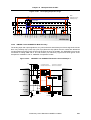
Chapter 1
Introduction
1.1 General
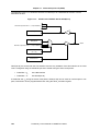
ERTEC 200 is a powerful communication block for development of industrial Ethernet devices with hard
real-time capabilities. ERTEC 200 contains a 32-bit RISC processor, an external memory interface with
SDRAM and SRAM controller, a local bus interface, a 2-channel real-time Ethernet interface with integrated PHYs, synchronous and asynchronous serial ports, and general purpose I/Os. Its robust construction, specific automation functions, and openness to the IT world are distinguishing features. The
ERTEC 200 is housed in a 304-pin plastic FBGA package (19 mm × 19 mm).
(1)
ARM946E-S Processor
ERTEC 200 uses an ARM946E-S processor with configurable clock frequencies of 50, 100 or
150 MHz. This processor however, is based on the ARM9E-S core that supports the ARM5vTE
instruction set architecture with 32-bit wide normal instructions and the 16-bit wide THUMB
instruction set.
It includes support for separate instruction and data caches as well as tightly coupled memory. In
case of ERTEC 200 8 kBytes of instruction cache (I-cache) and 4 kBytes of data cache (D-cache)
are available. The tightly coupled memory (TCM) has a size of 4 kBytes and can be accessed with
full CPU speed.
An integrated memory protection unit (MPU) allows to restrict access permission to eight programmable portions of the ERTEC 200 address space.
The processor core is extended with two on-chip interrupt controllers, one of which is connected to
the core’s FIQ input while the other one is connected to the IRQ input. The IRQ interrupt controller
handles up to 16 interrupt sources that can be prioritized; the FIQ interrupt controller can handle
up to 8 sources. Most interrupt sources are assigned to internal peripheral units, however GPIO
pins can be used as interrupt sources as well.
For easy debugging, ERTEC 200 is equipped with an ETM9 debug and trace module. In addition
to the on-chip debug capabilities of the ARM946E-S core, the ETM9 module allows instruction and
data trace. The ETM9 cell can be operated in full rate mode, as long as the CPU core frequency is
50 or 100 MHz; otherwise, half-rate mode must be selected.
(2)
Bus System
ERTEC 200’s internal bus structure is made up of a multilayer AHB bus and an APB bus. Both run
at a maximum speed of 50 MHz.
The multilayer AHB bus offers multimaster capability and up to four simultaneous bus communication processes between masters and slaves. Thus a very high availability of the AHB bus is
achieved. Potential bus masters are the ARM core, the LBU interface, the DMA controller and the
IRT switch; slaves are the external memory interface, the DMA controller, the IRT switch, the interrupt controller and the AHB-to-APB bridge.
The APB bus connects to the less demanding peripherals like UARTs, SPI, GPIOs etc.
(3)
On-chip Memories
ERTEC 200 has two categories of on-chip memories: the caches and the data TCM that are
regarded as belonging to the core, and a ROM area that is on-chip, but off-core. The on-chip ROM
has a size of 8 kBytes and is implemented as an APB peripheral. The boot ROM content is predefined and cannot be altered by the user. It contains a boot loader program with the ability to
choose among various other boot sources, if desired.
Preliminary User’s Manual A17988EE1V1UM00
17
Chapter 1 Introduction
(4)
External Memory Interface
The memory controller on ERTEC 200 supports synchronous DRAM as well as static memories
like SRAM or Flash. Additionally, static peripherals can be connected.
For SDRAM a data bus width of 16 or 32 bits can be configured; the addressing capabilities allow
connection of up to 128 MBytes of SDRAM. SDRAM is accessed with the clock speed of the
multilayer AHB bus, therefore the maximum SDRAM speed is 50 MHz with a CAS-latency of 2.
For static devices 4 chip selects with an address range of 16 MBytes each are prepared. They are
independently configurable to 8-, 16- or 32-bit bus width and to individual access timings. Slow
peripherals are supported with a ready signal input and a timeout function. Static chip select 0 can
be used for an external boot device - typically a flash memory - as an alternative to using the boot
loader in the on-chip ROM.
(5)
IRT Switch
The IRT switch block provides two Ethernet channels for 10 or 100 Mbps respectively half or full
duplex operation. The IRT switch is coupled to the multilayer AHB bus as a master and a slave and
to the external world via two integrated PHYs allowing direct connection to magnetics or optical
transceivers. For the use of external PHYs, the IRT switch can be re-configured to 2-channel MII
operation. A large internal Communication SRAM with 64 kBytes in size helps to support RT and
IRT data communication over Ethernet.
(6)
Local Bus Unit
The Local Bus unit (LBU) allows to run ERTEC 200 as a peripheral to an external host controller.
The LBU is a master to the multilayer AHB bus and has separate address (21-bit) and data (16-bit)
buses to the external world. Seen with the eyes of the external host, the LBU opens a total of four
configurable windows into the ERTEC 200, that allow to configure ERTEC 200 and to access all
internal resources.
(7)
DMA Controller
ERTEC 200 has a one-channel DMA controller for data transfers between peripherals, between
memories and between peripheral and memory. The DMA controller supports programmable
transfer sizes and auto-increment and address hold functions for data source and target. A set of
control registers can be accessed from the ARM946E-S core to set up transfers as required. The
completion of a DMA transfer is signalled with an interrupt or with a status bit.
(8)
Other Peripherals
The ERTEC 200 has several additional communication interfaces that can be accessed over the
AHB-to-APB bridge and the subsequent APB bus. These are a widely 16550-compatible UART, an
SPI channel, three timers, a watchdog, an additional fail-safe timer (F-timer) and a GPIO block
with up to 45 individually configurable I/Os. The interfaces share their pins with the GPIOs, so that
depending on the selected configuration a reduced number of GPIOs is available. 4 GPIOs can be
used as interrupt sources.
(9)
Clock and Power Supply
The ERTEC 200 can be operated with a single, external 25 MHz crystal. An internal oscillator and
PLL generate all required clocks for the ARM946E-S, the IRT block, the internal buses and other
peripherals. Alternatively, an external clock of 25 MHz can be supplied.
Two supply voltage levels are required for operation of ERTEC 200: The internal logic is running at
1.5 V; the I/Os and parts of the integrated PHYs are operating at 3.3 V.
18
Preliminary User’s Manual A17988EE1V1UM00
Chapter 1
Introduction
1.2 Device Features
• ARM946E-S Processor
-
Adjustable operating frequency (50/100/150 MHz)
System control coprocessor (CP15)
4 kBytes of Data-TCM
Interface with “Write buffer” on 32-bit multilayer AHB bus
8 kBytes I-cache and 4 kBytes D-cache with lock functionality
Memory Protection Unit
Cacheability attribute setting for regions
Read/write access rights for certain modes only
2 interrupt controllers with 16 inputs for IRQ and 8 inputs for FIQ
Debug/trace functionality by ETM9 module via JTAG interface
Trace in full rate mode at operating frequencies of 50 and 100 MHz
Trace in half rate mode at an operating frequency of 150 MHz
4-/8-bit trace data width selectable
Trace can be restricted to selected address ranges and memory regions
• External Memory Interface (EMIF)
• SDRAM memory controller
- Adjustable 16-/32-bit data bus width
- PC100 SDRAM-compatible (50 MHz clock frequency)
- Maximum of 128 MBytes/32-bit or 64 Mbytes/16-bit SDRAM
- Adjustable RAS/CAS latency (2, 3 for Write; 1, 2 for Read)
- 2-bit bank address (1/2/4 banks) via address bits A(1:0)
- 8-/9/-10-/11-bit column address A13, A(11:2)
- Maximum 13-bit row address A(14:2)
• Asynchronous memory controller for SRAM, Flash, I/O
- Adjustable 8-/16-/32-bit data bus width
- 4 chip selects with individual timing control
- Default setting for boot operation timing is “slow”
- Maximum of 16 Mbytes can be addressed for each chip select
- Chip select CS_PER0_N can be used for boot memory
- Data bus width of boot ROM at CS_PER0_N is selectable via BOOT(3:0) pins
- Adjustable timeout monitoring
- DTR_N (direction) and OE_DRIVER_N (enable) control signals for direct control of an
external driver for chip select signals CS_PER(3:0)_N
• IRT Switch
-
Two Fast Ethernet ports with integrated PHYs
10BASE-T and 100BASE-TX/FX support
Full duplex/half duplex mode support
Supports RT and IRT data traffic
Autonegotiation
Broadcast filter
IEEE 1588 time stamping
64 kBytes of Communication SRAM
• Local Bus Unit (LBU)
-
16-bit data bus width, 21-bit address bus width
Host access to LBU paging registers via chip select signal LBU_CS_R_N
Host access to any address area of ERTEC 200 via chip select signal LBU_CS_M_N
Maximum of 4 pages can be addressed
Adjustable page-range and page-offset for each page; reconfigurable at any time
Preliminary User’s Manual A17988EE1V1UM00
19
Chapter 1 Introduction
• DMA Controller
-
One-channel DMA controller
Supports data transfers between internal and external memories
Supports data transfers between peripherals and internal memory
Selectable transfer width (8/16/32 bits) and block size
4 request inputs for synchronization with peripherals
Change/hold address modes selectable
DMA control via hard- or software
End of transfer can be signalled with an interrupt
• Other I/O Interfaces
• 45-bit General Purpose I/O (GPIO)
- Input/outputs GPIO(31:0) can be assigned on a bit-by-bit basis
- Input/outputs GPIO(44:32) can be used alternatively to LBU interface
- All GPIOs equipped with internal pull-up resistor
- 4 GPIO inputs are interruptible (active Low level is not a supported interrupt level)
- GPIO(31:0) can be assigned up to 4 different functions (see Table 11-3)
- 8-/16-/32-bit access to registers is possible
• UART
- Based on ARM PrimeCellTM UART PL010 and widely 16550 compatible
• SPI
- Supports Motorola SPI, TI SSI and National Instruments microwire modes
- Programmable data frame size and bit rate
- Master and slave mode capability
- Send and Receive FIFOs with 8 16-bit entries
- Group and overrun error interrupts
• Timers
- Two 32-bit down counters with load/reload capability (T0/1)
- Start, stop, continue functions and interrupts
- Cascadable to a 64-bit timer and additional 8-bit prescaler selectable
- Timers run on 50 MHz internal clock
- Single 16-bit up counter with load/reload capability (T2)
- Start, stop functions and interrupts
- Timer runs on 50 MHz internal clock
- Additional 32-bit fail-safe F-Timer
- Runs from external clock F_CLK
• Watchdog
- 32-bit count-down watchdog 0 with output pin WD_WDOUT0_N
- 36-bit count-down watchdog 1
- Load/reload function
- Write protection for watchdog
- Watchdog interrupt on the FIQ interrupt controller
20
Preliminary User’s Manual A17988EE1V1UM00
Chapter 1
Introduction
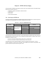
1.3 Ordering Information
Device
Part Number
µPD800261F1-523-HN2
ERTEC 200
µPD800261F1-523-HN2-A
Remark:
Package
P-FBGA304, 19 × 19 mm
Products with -A at the end of the part number are lead-free products.
Preliminary User’s Manual A17988EE1V1UM00
21
Chapter 1 Introduction
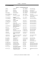
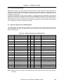
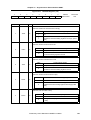
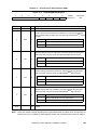
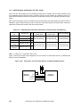
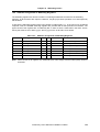
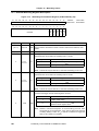
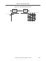
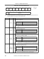
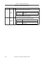
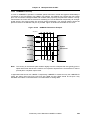
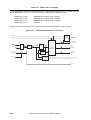
1.4 Pin Configuration
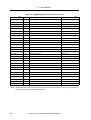
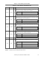
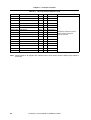
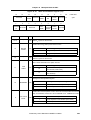
Figure 1-1:
Pin Configuration of ERTEC 200 - 304-Pin Plastic FBGA (19 mm × 19 mm)
22
21
20
19
18
17
16
15
14
13
12
11
10
9
8
7
6
5
4
3
2
1
INDEX MARK
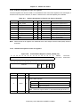
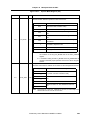
Table 1-1:
Pin
Number
Pin Name
AA W U R N L J G E C A
AB Y V T P M K H F D B
Pin Configuration of ERTEC 200 (1/5)
Pin
Number
Pin Name
A2
VDD IO
A21
GND Core
A3
A1
B1
GND IO
A4
WR_N
B2
A3
A5
CS_PER1_N
B3
A2
A6
CS_PER2_N
B4
A0
A7
GPIO26
B5
RD_N
A8
GND IO
B6
CS_PER3_N
A9
VDD IO
B7
RESET_N
A10
VDD IO
B8
GPIO30
A11
GPIO21/SPI1_SFRMOUT
B9
GPIO25/TGEN_OUT1_N
A12
GND IO
B10
GPIO27
A13
GPIO16/SPI1_SSPCTLOE
B11
GPIO24/PLL_EXT_IN_N
A14
VDD IO
B12
GPIO18/SPI1_SSPRXD
A15
REF_CLK
B13
F_CLK
A16
GPIO12/UART-CTS-N
B14
CLKP_A
A17
GPIO9/UART-RXD
B15
GPIO13
A18
VDD IO
B16
GPIO10/UART-DCD-N
A19
GPIO4/P1-LINK-LED_N
B17
GPIO8/UART-TXD
A20
GND IO
B18
GPIO6/P1-RX-LED_N/P1-TX-LED_N/P1-ACTIVE-LED_N
22
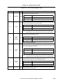
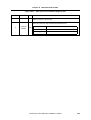
Preliminary User’s Manual A17988EE1V1UM00
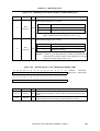
Chapter 1
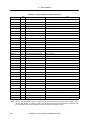
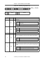
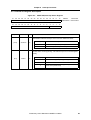
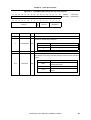
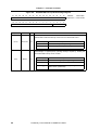
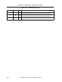
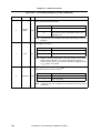
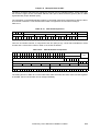
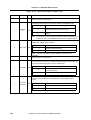
Table 1-1:
Pin
Number
Introduction
Pin Configuration of ERTEC 200 (2/5)
Pin Name
Pin
Number
Pin Name
B19
GPIO3/P2-SPEED-100LED_N/P2-SPEED-10LED_N
E13
VDD Core
B20
GPIO1/P2 -DUPLEX-LED_N
E14
GPIO15/WD_WDOUT0_N
B21
GND IO
E15
GPIO14/DBGACK
B22
VDD IO
E16
GPIO11/UART-DSR-N
C1
A6
E17
GND Core
C2
A5
E18
VDD Core
C21
P1TDxP
E19
GNDNote
C22
P1TDxN
E21
P1RDxN
D1
A8
E22
P1RDxP
D2
A7
F1
A12
D4
A4
F2
A11
D5
CS_PER0_N
F4
A20/CONFIG3
D6
VDD Core
F5
GND Core
D7
RDY_PER_N
F6
VDD Core
D8
OE_DRIVER_N
F7
GND Core
D9
VDD Core
F8
GND IO
D10
GPIO23/SPI1_SCLKIN
F9
GPIO28
D11
GPIO20/SPI1_SCLKOUT
F10
GPIO22/SPI1_SFRMIN/DBGACK
D12
VDD Core
F13
PLL_AGND
D13
GPIO19/SPI1_SSPTXD
F14
GPIO17/SPI1_SSPOE
D14
CLKP_B
F15
GND IO
D15
GPIO7/P2-RX-LED_N/P2-TX-LED_N/P2-ACTIVE-LED_N
F16
GND Core
D16
GPIO5/P2-LINK-LED_N
F17
VDD Core
D17
GPIO2/P1-SPEED-100LED_N/P1-SPEED-10LED_N
F18
GND (PECL)
D18
VDD Core
F19
P1SDxN
D19
GPIO0/P1-DUPLEX-LED_N
F21
GNDNote
D21
VDDQ (PECL)
F22
VDD33ESD
D22
VDDQ (PECL)
G1
A14
E1
A10
G2
A13
E2
A9
G4
A21/CONFIG4
E4
A19/CONFIG2
G5
GND IO
E5
VDD Core
G6
GND Core
E6
GND Core
G17
DGND2
E7
DTR_N/BOOT0
G18
DVDD1
E8
GPIO31/DBGREQ
G19
P1SDxP
E9
GPIO29
G21
P1RxP
E10
GND IO
G22
P1RxN
E11
GND Core
H1
VDD IO
E12
PLL_AVDD
H2
A15/BOOT1
Note: Connect to GND to improve heat dissipation; pins may as well be left open.
Preliminary User’s Manual A17988EE1V1UM00
23
Chapter 1 Introduction
Table 1-1:
Pin
Number
Pin Name
Pin Configuration of ERTEC 200 (3/5)
Pin
Number
Pin Name
H4
A23/CONFIG6
M4
WE_SDRAM_N
H5
A22/CONFIG5
M5
RAS_SDRAM_N
H6
GND IO
M18
P2VSSATX1
H17
GNDNote
M19
GNDNote
H18
GND33ESD
M21
P2TxN
H19
DVDD2
M22
P2TxP
H21
DGND1
N1
VDD IO
H22
VDDACB
N2
D1
J1
GND IO
N4
BE0_DQM0_N
J2
A16/BOOT2
N5
D20
J4
BE2_DQM2_N
N6
D21
J5
leave open
N17
P2VSSARX
J6
D18
N18
P2VDDARXTX
J17
P1VSSARX
N19
GNDNote
J18
GNDNote
N21
GNDNote
J19
P1VDDARXTX
N22
GNDNote
J21
P1TxN
P1
D2
J22
P1TxP
P2
D3
K1
A18/CONFIG1
P4
D25
K2
A17/BOOT3
P5
BE3_DQM3_N
K4
D16
P6
D22
K5
D17
P17
GNDNote
K6
D19
P18
GNDNote
K17
P1VSSATX1
P19
GNDNote
K18
P1VSSATX2
P21
P2RxP
K19
VDDAPLL
P22
P2RxN
K21
GNDNote
R1
D4
K22
GNDNote
R2
VDD Core
L1
CS_SDRAM_N
R4
D26
L2
CAS_SDRAM_N
R5
D23
L4
VDD Core
R6
D24
L5
GND Core
R17
DGND3
L18
VSSAPLLCB
R18
GNDNote
L19
P2VSSATX2
R19
VDDQ (PECL)
L21
EXTRES
R21
DVDD4
L22
leave open
R22
DVDD3
M1
CLK_SDRAM
T1
GND IO
M2
D0
T2
D5
Note: Connect to GND to improve heat dissipation; pins may as well be left open.
24
Preliminary User’s Manual A17988EE1V1UM00
Chapter 1
Table 1-1:
Pin
Number
Pin Name
Introduction
Pin Configuration of ERTEC 200 (4/5)
Pin
Number
Pin Name
T4
D27
V15
LBU_D13/SMI_MDIO
T5
leave open
V16
LBU_D14/RES_PHY_N
T6
GND Core
V17
GND IO
T17
DGND4
V18
VDD Core
T18
GND (PECL)
V19
P2SDxP
T19
GND (PECL)
V21
VDDQ (PECL)
T21
VDD Core
V22
GNDNote
T22
GNDNote
W1
D9
U1
D6
W2
D10
U2
D7
W4
D29
U4
D28
W5
D30
U5
GND IO
W6
D31
U6
VDD Core
W7
TCK
U7
GND IO
W8
TAP_SEL
U8
VDD Core
W9
LBU_A16/GPIO32
U9
TDI
W10
LBU_A17/GPIO33
U10
TRST_N
W11
LBU_A15/COL_P2
U13
LBU_SEG_1/GPIO38
W12
LBU_A19/GPIO35
U14
LBU_CS_M_N/GPIO40
W13
VDD Core
U15
GND IO
W14
LBU_D12/SMI_MDC
U16
GND Core
W15
LBU_D1/TXD_P11
U17
VDD Core
W16
LBU_D15/GPIO41
U18
P2SDxN
W17
VDD Core
U19
leave open
W18
LBU_IRQ1_N/GPIO44
U21
P2RDxN
W19
LBU_RDY_N/GPIO42
U22
P2RDxP
W21
P2TDxN
V1
BE1_DQM1_N
W22
VDD IO
V2
D8
Y1
VDD IO
V4
VDD Core
Y2
D11
V5
VDD Core
Y21
P2TDxP
V6
GND Core
Y22
VDD IO
V7
TMS
AA1
D12
V8
SRST_N
AA2
D13
V9
TDO
AA3
D15
V10
LBU_A18/GPIO34
AA4
LBU_A1/RXD_P11/ETMEXTIN1
V11
GND Core
AA5
LBU_A2/RXD_P12/TRACEPKT7
V12
LBU_A20/GPIO36
AA6
LBU_A4/CRS_P1/TRACEPKT5
V13
LBU_SEG_0/GPIO37
AA7
LBU_A6/RX_DV_P1/TRACEPKT3
V14
GND Core
AA8
LBU_A8/RXD_P20/TRACEPKT1
Note: Connect to GND to improve heat dissipation; pins may as well be left open.
Preliminary User’s Manual A17988EE1V1UM00
25
Chapter 1 Introduction
Table 1-1:
Pin
Number
Pin Configuration of ERTEC 200 (5/5)
Pin Name
Pin
Number
Pin Name
AA9
LBU_A10/RXD_P22/TRACESYNC
AB5
LBU_A3/RXD_P13/TRACEPKT6
AA10
LBU_A11/RXD_P23/PIPESTA2
AB6
LBU_A5/RX_ER_P1/TRACEPKT4
AA11
LBU_A13/RX_ER_P2/PIPESTA0
AB7
LBU_A7/COL_P1/TRACEPKT2
AA12
LBU_WR_N/TX_CLK_P1
AB8
LBU_A9/RXD_P21/TRACEPKT0
AA13
LBU_BE1_N/RX_CLK_P2
AB9
VDD IO
AA14
LBU_D0/TXD_P10
AB10
LBU_A12/CRS_P2/PIPESTA1
AA15
VDD Core
AB11
LBU_A14/RX_DV_P2
AA16
LBU_D3/TXD_P13
AB12
LBU_CS_R_N/GPIO39
AA17
LBU_D5/TX_ERR_P1
AB13
LBU_RD_N/TX_CLK_P2
AA18
LBU_D7/TXD_P21
AB14
LBU_BE0_N/RX_CLK_P1
AA19
LBU_D9/TXD_P23
AB15
VDD IO
AA20
LBU_D10/TX_EN_P2
AB16
LBU_D2/TXD_P12
AA21
LBU_IRQ0_N/GPIO43
AB17
LBU_D4/TX_EN_P1
AA22
GND Core
AB18
LBU_D6/TXD_P20
AB2
D14
AB19
LBU_D8/TXD_P22
AB3
LBU_A0/RXD_P10/ETMEXTOUT
AB20
VDD IO
AB4
TRACECLK
AB21
LBU_D11/TX_ERR_P2
26
Preliminary User’s Manual A17988EE1V1UM00
Chapter 1
Introduction
1.5 Pin Identification
Table 1-2:
Pin Identification (1/2)
A(23:0)
: Address bus
SPI1_SSPRXD
: SPI receive data
D(31:0)
: Data bus
SPI1_SSPTXD
: SPI transmit data
WR_N
: Write strobe
SPI1_SCLKOUT
: SPI clock out
RD_N
: Read strobe
SPI1_SFRMOUT
: SPI serial frame output
CLK_SDRAM
: Clock to SDRAM
SPI1_SFRMIN
: SPI serial frame input
BE(3:0)_DQM(3:0)_N
: Byte enable
SPI1_SCLKIN
: SPI clock in
CS_SDRAM_N
: Chip select to SDRAM
SPI1_SSPCTLOE
: SPI clock and serial frame
output enable
RAS_SDRAM_N
: Row address strobe to
SDRAM
SPI1_SSPOE
: SPI output enable
CAS_SDRAM_N
: Column address strobe to
SDRAM
TXD_P(2:1) 0
: MII transmit data bit 0
WE_SDRAM_N
: RD/WR SDRAM
TXD_P(2:1) 1
: MII transmit data bit 1
CS_PER(3:0)_N
: Chip select
TXD_P(2:1) 2
: MII transmit data bit 2
RDY_PER_N
: Ready signal
TXD_P(2:1) 3
: MII transmit data bit 3
DTR_N
: Direction signal for external
driver or scan clock
RXD_P(2:1) 0
: MII receive data bit 0
OE_DRIVER_N
: Enable signal for external
driver or scan clock
RXD_P(2:1) 1
: MII receive data bit 1
BOOT(3:0)
: Boot mode
RXD_P(2:1) 2
: MII receive data bit 2
CONFIG(6:1)
: System configuration
RXD_P(2:1) 3
: MII receive data bit 3
GPIO(44:0)
: GPIO pins
TX_EN_P(2:1)
: MII transmit enable
UART-TXD
: UART transmit data output
TX_ERR_P(2:1)
: MII transmit error
UART-RXD
: UART receive data input
RX_ER_P(2:1)
: MII receive error
UART-DCD_N
: UART carrier detection
signal
CRS_P(2:1)
: MII carrier sense
UART-DSR_N
: UART data set ready signal
RX_DV_P(2:1)
: MII receive data valid
UART-CTS_N
: UART transmit enable
signal
COL_P(2:1)
: MII collision
LBU_A(20:0)
: LBU address bus
RX_CLK_P(2:1)
: MII receive clock
LBU_D(15:0)
: LBU data bus
TX_CLK_P(2:1)
: MII transmit clock
LBU_WR_N
: LBU write control
SMI_MDC
: MII SMI clock
LBU_RD_N
: LBU read control
SMI_MDIO
: MII SMI input/output
LBU_BE(1:0)_N
: LBU byte enable
RES_PHY_N
: Reset to PHY
LBU_SEG_(1:0)
: LBU page selection
P(2:1)TxP
: Differential transmit output
LBU_IRQ_(1:0)_N
: LBU interrupt request
P(2:1)TxN
: Differential transmit output
LBU_RDY_N
: LBU ready signal
P(2:1)RxP
: Differential receive input
LBU_CS_M_N
: LBU chip select to ERTEC
200 internal resources
P(2:1)RxN
: Differential receive input
LBU_CS_R_N
: LBU chip select to page
configuration registers
P(2:1)TDxP
: FX differential transmit output
Preliminary User’s Manual A17988EE1V1UM00
27
Chapter 1 Introduction
Table 1-2:
Pin Identification (2/2)
P(2:1)TDxN
: FX differential transmit output
DBGREQ
: Debug request to ARM9
P(2:1)RDxP
: FX differential receive input
DBGACK
: Debug acknowledge
P(2:1)RDxN
: FX differential receive input
TAP_SEL
: Select TAP controller
P(2:1)SDxP
: FX differential SD input
CLKP_A
: Quartz connection
P(2:1)SDxN
: FX differential SD input
CLKP_B
: Quartz connection
EXTRES
: Reference resistor 12.4 kΩ
REF_CLK
: Reference clock output
P(2:1)DUPLEX-LED_N
: PHY LED
F_CLK
: Clock for F-counter
P(2:1)LINK-LED_N
: PHY LED
RESET_N
: Power On reset
P(2:1)-SPEED-100LED_N
(TX/FX)
: PHY LED
WD_WDOUT0_N
: Watchdog output
: PHY LED
VDD Core
: Power supply for core,
1.5 V
P(2:1)-RX-LED_N
: PHY LED
GND Core
: GND for core
P(2:1)-TX-LED_N
: PHY LED
VDD IO
: Power supply for IO, 3.3 V
P(2:1)-ACTIVE-LED_N
: PHY LED
GND IO
: GND for IO
PLL_EXT_IN_N
: MC_PLL input signal
PLL_AVDD
: Analog power supply for
PLL, 1.5 V
TGEN_OUT1_N
: MC_PLL output signal
PLL_AGND
: Analog GND for PLL
TRACEPKT(7:0)
: Trace pins of ETM
VDDQ (PECL)
: Power supply for PECL
buffers, 3.3 V
ETMEXTOUT
: ETM output signal
GND (PECL)
: GND for PECL buffers
ETMEXTIN1
: ETM input signal
DVDD(4:1)
: Digital power supply for
PHYs, 1.5 V
PIPESTA(2:0)
: Trace pipeline status
DGND(4:1)
: Digital GND for PHYs
TRACESYNC
: Trace sync signal
P(2:1)VDDARXTX
: Analog port Tx/Rx power
supply, 1.5 V
TRACECLK
: ETM trace or scan clock
P(2:1)VSSARX
: Analog port GND
TRST_N
: JTAG reset
P(2:1)VSSATX(2:1)
: Analog port GND
TCK
: JTAG clock
VDDAPLL
: Analog central power supply, 1.5 V
TDI
: JTAG data in
VDDACB
: Analog central power supply, 3.3 V
TMS
: JTAG test mode select
VSSAPLLCB
: Analog central GND
TDO
: JTAG data out
VDD33ESD
: Analog test power supply,
3.3 V
SRST_N
: Hardware reset for debug
usage
GND33ESD
: Analog test GND
P(2:1)-SPEED-10LED_N
28
Preliminary User’s Manual A17988EE1V1UM00
Chapter 1
Introduction
1.6 Configuration of Functional Blocks
1.6.1 Block Diagram of ERTEC 200
Figure 1-2:
Internal Block Diagram
%XTERNAL-EMORY)NTERFACE
4RACE
0ORT
*4!'$EBUG
-(Z
2%&?#,+
%-)&
-ASTER
3LAVE
3LAVE
%4!0"
-ASTER
3LAVE
-(Z
-(Z
)#ACHEK"YTES
$#ACHEK"YTES
$4#-K"YTES
-(Z
3LAVE
$-!
#ONTROLLER
!2)NTERRUPT
#ONTROLLER
!2-
#LOCK
"3
4!0
WITH
%XTERNAL
-EMORY
)NTERFACE
2ESET
#LOCK
5NIT
"OOT
2/K"YTES
3LAVE
!2-%3
'0)/
BIT-(Z
!("
7RAPPER
3LAVE
-ASTER
-#"USBIT-(Z
-ASTER
,OCAL
"US5NIT
3#"USBIT-(Z
#OMMUNI
CATION
32!-
3WITCH#ONTROL
K"YTES
,"5
BIT
-58
,OCAL"US
'0)/%4--))
%THERNET
#HANNEL
%THERNET
#HANNEL
0ORT
0ORT
0(9
0(9
0ORT
0ORT
-$)0ORT
-$)0ORT
30)
)NTERFACE
X4IMER
7ATCHDOG
&4IMER
3YSTEM
#ONTROL
2EGISTERS
0ERIPHERAL0ORTS
3LAVE
!("
7RAPPER
3LAVE
-ASTER
5!24
3LAVE
-58!RB
3LAVE
-ULTILAYER!("
BIT-(Z
)NPUT
STAGE
3LAVE
)NPUT
STAGE
!("!0"
"RIDGE
-ASTER
)NPUT
STAGE
$ECODE
-58!RB
$ECODE
3LAVE
)NPUT
STAGE
-58!RB
'0)/
5!24
30)
4IMER
7ATCHDOG
-#?0,,
)24
3WITCH
-ACRO
Preliminary User’s Manual A17988EE1V1UM00
29
Chapter 1 Introduction
1.6.2 On-chip Units
(1)
CPU (ARM946E-S)
ERTEC 200 uses an ARM946E-S 32-bit RISC processor core running at a maximum speed of
150 MHz. This core processes 32-bit instructions according to the ARM5v5TE instruction set
architecture as well as 16-bit wide THUMB instructions. Instruction throughput is increased using
a five-stage pipeline, 8 kBytes of I-cache, 4 kBytes of D-cache and 4 kBytes of D-TCM.
(2)
Multilayer AHB Bus
The Multilayer AHB bus is the data highway within ERTEC 200. It connects all major functional
blocks with a 32-bit, 50 MHz segmented bus structure, that is able to run four bus transfers in parallel without blocking.
(3)
External Memory Interface
Access to external memories is provided with a double memory controller that supports
128 MBytes of standard SDRAM with an access speed of 50 MHz and a total of 64 MBytes of
static memory with one dynamic and four static chip select signals. The static chip select signals
can be used for SRAM, Flash and peripheral devices. External bus width is configurable to
16-/32-bit for SDRAM and 8-/16-/32-bit for the static portion of the interface. Access timings are
individually selectable for each chip select.
(4)
Interrupt Controller
The ARM processor core on ERTEC 200 has a “normal” interrupt input (IRQ) and a fast interrupt
input (FIQ). With the on-chip interrupt controller, the interrupt processing capabilities are extended
to 16 IRQs and 8 FIQs with prioritization and vectorization. These interrupts are partly assigned to
internal resources and partly accessible to the external world via GPIO pins.
(5)
IRT Switch
The IRT switch block on ERTEC 200 provides two 10/100 Mbps Ethernet channels; due to special
control features and the large Communication SRAM of 64 kBytes, all channels support real-time
and isochronous real-time communication. Connection to an Ethernet network is realized with
integrated PHYs that support 10BASE-T and 100BASE-TX/FX modes. The internal MII interface
between MACs and PHYs can be made available for diagnosis purposes.
(6)
Local Bus Interface
ERTEC 200 has a local bus interface (LBU) to an external host controller; it offers 21 address bits
and 16 data bits. ERTEC 200 is a slave with respect to this interface. The external host can look
through four configurable (in size and position) windows into ERTEC 200’s address space. Read/
write control is either done with separate read and write lines or with a common read/write line.
(7)
DMA Controller
The integrated DMA controller reduces CPU load for data transfers between memory and memory
respectively between memory and peripheral. Address increment/hold modes as well as soft- or
hardware handshake between the DMA transfer and the CPU are supported.
(8)
AHB to APB Bridge
The slower peripherals of ERTEC 200 are connected to an internal 32-bit/50 MHz APB bus that
can be accessed via an AHB-to-APB bridge from the AHB side. From the programmers point of
view, these peripherals are memory mapped like any other.
30
Preliminary User’s Manual A17988EE1V1UM00
Chapter 1
(9)
Introduction
Boot ROM
ERTEC 200 has 8 kBytes of 32-bit wide boot ROM; it is pre-defined with a boot-loader program
that supports various external boot sources: external Flash via EMIF, serial Flash or EEPROM via
SPI, LBU with an external host and UART. Selection of boot sources is done via the BOOT(3:0)
configuration pins.
(10) GPIO Block
ERTEC 200 has a total of 45 GPIO pins that are individually programmable as input or output.
Four of these GPIOs can be used as interrupts. 38 of these GPIOs are shared with other interfaces like UART, SPI and LBU.
(11) UART
The integrated UART can be used for asynchronous, serial communication. It is based on the
ARM PrimeCellTM PL010 and is widely 16550-compatible. 2 data lines and 3 handshake lines are
used. The internal 50 MHz clock is used for the UART operation and with a baud rate generator
standard baud rates up to 115 kbps can be selected.
(12) SPI
The SPI is used for synchronous serial communication according to Motorola, TI and National
quasi-standards. Frame size, protocol and speed are software programmable. The maximum
transmission speed is 25 MHz in master mode and 4.16 MHz in slave mode. The SPI is based on
the ARM PrimeCellTM PL021.
(13) Timers, Watchdog
ERTEC 200 has four timers and two watchdogs. Three of the timers are driven with the internal
50 MHz clock and based on 32-bit respectively 36-bit down counters that are cascadable and that
can be configured with an additional 8-bit prescaler, and an additional 16-bit up counter. The
fourth timer, the F-timer, runs under the control of an external clock.
The watchdog timers are also based on 32-bit and 36-bit down-counters. Watchdog 0 (32-bit) is
generating an output signal on the WD_WDOUT0_N pin; watchdog 1 (36-bit) generates a reset.
(14) System Control Registers
A bundle of specific system control registers help to configure the processor and to analyse
internal problems like access right and/or address range violations or timeouts.
Preliminary User’s Manual A17988EE1V1UM00
31
[MEMO]
32
Preliminary User’s Manual A17988EE1V1UM00
2. Pin Functions
2.1 List of Pin Functions
Table 2-1:
Pin Name
External Memory Interface Pin Functions
I/O
Function
Alternate Function
A(23:18)
I/ONote External memory address bus (23:18)
CONFIG(6:1)Note
A(17:15)
I/ONote External memory address bus (17:15)
BOOT(3:1)Note
A(14:0)
O
External memory address bus (14:0)
-
D(31:0)
I/O
External memory data bus (31:0)
-
WR_N
O
Write strobe signal
-
RD_N
O
Read strobe signal
-
CLK_SDRAM
O
Clock to SDRAM
-
CS_SDRAM_N
O
Chip select to SDRAM
-
RAS_SDRAM_N
O
Row address strobe SDRAM
-
CAS_SDRAM_N
O
Column address strobe to SDRAM
-
WE_SDRAM_N
O
RD/WR signal to SDRAM
-
CS_PER(3:0)_N
O
Chip select to static memories and peripherals
-
BE(3:0)_DQM(3:0)_N
O
Byte enable signal
-
I
Ready signal
-
Direction signal for external driver or scan clock
BOOT0Note
Enable signal for external driver or scan clock
-
RDY_PER_N
DTR_N
OE_DRIVER_N
I/ONote
O
Note: The BOOT(3:0) and CONFIG(6:1) pins are used as inputs and read into the BOOT_REG respectively
CONFIG_REG system configuration registers during the active Power On reset phase. After a reset,
these pins are available as normal function pins and used as outputs.
Preliminary User’s Manual A17988EE1V1UM00
33
2. Pin Functions
Table 2-2:
Pin Name
Local Bus Interface Pin Functions (1/2)
I/ONote
Alternate FunctionNote
Function
LBU_A(20:16)
I
LBU address bits
GPIO(36:32)
LBU_A15
I
LBU address bit 15
COL_P2
LBU_A14
I
LBU address bit 14
RX_DV_P2
LBU_A13
I
LBU address bits 13
RX_ER_P2/PIPESTA0
LBU_A12
I
LBU address bit 12
CRS_P2/PIPESTA1
LBU_A11
I
LBU address bit 11
RXD_P23/PIPESTA2
LBU_A10
I
LBU address bit 10
RXD_P22/TRACESYNC
LBU_A9
I
LBU address bit 9
RXD_P21/TRACEPKT0
LBU_A8
I
LBU address bit 8
RXD_P20/TRACEPKT1
LBU_A7
I
LBU address bit 7
COL_P1/TRACEPKT2
LBU_A6
I
LBU address bit 6
RX_DV_P1/TRACEPKT3
LBU_A5
I
LBU address bit 5
RX_ER_P1/TRACEPKT4
LBU_A4
I
LBU address bit 4
CRS_P1/TRACEPKT5
LBU_A3
I
LBU address bit 3
RXD_P13/TRACEPKT6
LBU_A2
I
LBU address bit 2
RXD_P12/TRACEPKT7
LBU_A1
I
LBU address bit 1
RXD_P11/ETMEXTIN1
LBU_A0
I
LBU address bit 0
RXD_P10/ETMEXTOUT
LBU_D15
I/O
LBU data bit 15
GPIO41
LBU_D14
I/O
LBU data bit 14
RES_PHY_N
LBU_D13
I/O
LBU data bit 13
SMI_MDIO
LBU_D12
I/O
LBU data bit 12
SMI_MDC
LBU_D11
I/O
LBU data bit 11
TX_ERR_P2
LBU_D10
I/O
LBU data bit 10
TX_EN_P2
LBU_D9
I/O
LBU data bit 9
TXD_P23
LBU_D8
I/O
LBU data bit 8
TXD_P22
LBU_D7
I/O
LBU data bit 7
TXD_P21
LBU_D6
I/O
LBU data bit 6
TXD_P20
LBU_D5
I/O
LBU data bit 5
TX_ERR_P1
LBU_D4
I/O
LBU data bit 4
TX_EN_P1
LBU_D3
I/O
LBU data bit 3
TXD_P13
LBU_D2
I/O
LBU data bit 2
TXD_P12
LBU_D1
I/O
LBU data bit 1
TXD_P11
LBU_D0
I/O
LBU data bit 0
TXD_P10
LBU_WR_N
I
LBU write control signal
TX_CLK_P1
LBU_RD_N
I
LBU read control signal
TX_CLK_P2
LBU_BE(1:0)_N
I
LBU byte enable
RX_CLK_P(2:1)
LBU_SEG_1
I
LBU page selection signal
GPIO38
LBU_SEG_0
I
LBU page selection signal
GPIO37
LBU_IRQ_1_N
O
LBU interrupt request signal
GPIO44
LBU_IRQ_0_N
O
LBU interrupt request signal
GPIO43
34
Preliminary User’s Manual A17988EE1V1UM00
2.
Table 2-2:
Pin Name
Pin Functions
Local Bus Interface Pin Functions (2/2)
I/ONote
Alternate FunctionNote
Function
LBU_RDY_N
O
LBU ready signal
GPIO42
LBU_CS_M_N
I
LBU chip select for ERTEC 200 internal resources GPIO40
LBU_CS_R_N
I
LBU chip select for page configuration registers
GPIO39
Note: Local bus interface pins are alternatively used as MII diagnosis, trace or GPIO pins; in this table the I/O
type is listed for the local bus function.
Preliminary User’s Manual A17988EE1V1UM00
35
2. Pin Functions
Table 2-3: MII/SMI Diagnosis Interface Pin Functions
Pin NameNote
I/O
Function
Alternate FunctionNote
SMI_MDC
O
Serial management interface clock
LBU_D12
SMI_MDIO
O
Serial management interface data input/output
LBU_D13
RES_PHY_N
O
Reset signal to PHYs
LBU_D14
TXD_P2(3:0)
O
Transmit data port 2 bits
LBU_D(9:6)
RXD_P23
O
Receive data port 2 bit 3
LBU_A11/PIPESTA2
RXD_P22
O
Receive data port 2 bit 2
LBU_A10/TRACESYNC
RXD_P21
O
Receive data port 2 bit 1
LBU_A9/TRACEPKT0
RXD_P20
O
Receive data port 2 bit 0
LBU_A8/TRACEPKT1
TX_EN_P2
O
Transmit enable port 2
LBU_D10
CRS_P2
O
Carrier sense port 2
LBU_A12
RX_ER_P2
O
Receive error port 2
PIPESTA0
TX_ERR_P2
O
Transmit error port 2
LBU_D11
RX_DV_P2
O
Receive data valid port 2
LBU_A14
COL_P2
O
Collision port 2
LBU_A15
RX_CLK_P2
O
Receive clock port 2
LBU_BE1_N
TX_CLK_P2
O
Transmit clock port 2
LBU_RD_N
TXD_P1(3:0)
O
Transmit data port 1 bits
LBU_D(3:0)
RXD_P13
O
Receive data port 1 bit 3
LBU_A3/TRACEPKT6
RXD_P12
O
Receive data port 1 bit 2
LBU_A2/TRACEPKT7
RXD_P11
O
Receive data port 1 bit 1
LBU_A1/ETMEXTIN1
RXD_P10
O
Receive data port 1 bit 0
LBU_A0/ETMEXTOUT
TX_EN_P1
O
Transmit enable port 1
LBU_D4
CRS_P1
O
Carrier sense port 1
LBU_A4/TRACEPKT5
RX_ER_P1
O
Receive error port 1
LBU_A5/TRACEPKT4
TX_ERR_P1
O
Transmit error port 1
LBU_D5
RX_DV_P1
O
Receive data valid port 1
LBU_A6/TRACEPKT3
COL_P1
O
Collision port 1
LBU_A7/TRACEPKT2
RX_CLK_P1
O
Receive clock port 1
LBU_BE0_N
TX_CLK_P1
O
Transmit clock port 1
LBU_WR_N
Note: MII/SMI diagnosis interface pins are alternatively used as local bus interface or trace pins; in this table the
I/O type is listed for the MII/SMI diagnosis function
36
Preliminary User’s Manual A17988EE1V1UM00
2.
Pin Functions
Table 2-4: PHY Interface Pin Functions
Pin Name
I/O
Function
Alternate Function
P(2:1)TxN
O
Differential transmit data output
-
P(2:1)TxP
O
Differential transmit data output
-
P(2:1)TDxN
O
Differential FX transmit data output
-
P(2:1)TDxP
O
Differential FX transmit data output
-
P(2:1)RxN
I
Differential receive data input
-
P(2:1)RxP
I
Differential receive data input
-
P(2:1)RDxN
I
Differential FX receive data input
-
P(2:1)RDxP
I
Differential FX receive data input
-
P(2:1)SDxN
I
Differential FX signal detect input
-
P(2:1)SDxP
I
Differential FX signal detect input
-
External reference resistor (12.4 kΩ) Note
-
EXTRES
I/O
DVDD(4:1)
I
Digital power supply, 1.5 V
-
DGND(4:1)
I
Digital GND
-
P(2:1)VSSATX(2:1)
I
Analog port GND
-
P(2:1)VDDARXTX
I
Analog port RX/TX power supply, 1.5 V
-
P(2:1)VSSARX
I
Analog port GND
-
VDDAPLL
I
Analog central power supply, 1.5 V
-
VDDACB
I
Analog central power supply, 3.3 V
-
VSSAPLLCB
I
Analog central GND
-
VDD33ESD
I
Analog test power supply, 3.3 V
-
VSS33ESD
I
Analog test GND
-
Note: The external resistor must have a maximum tolerance of 1%.
Preliminary User’s Manual A17988EE1V1UM00
37
2. Pin Functions
Table 2-5: General Purpose I/O Pin Functions
Pin Name
I/ONote
Alternate FunctionNote
GPIO(44:43)
I/O
General purpose I/O signal
LBU_IRQ(1:0)_N
GPIO42
I/O
General purpose I/O signal
LBU_RDY_N
GPIO41
I/O
General purpose I/O signal
LBU_D15
GPIO40
I/O
General purpose I/O signal
LBU_CS_M_N
GPIO39
I/O
General purpose I/O signal
LBU_CS_R_N
GPIO(38:37)
I/O
General purpose I/O signal
LBU_SEG(1:0)_N
GPIO(36:32)
I/O
General purpose I/O signal
LBU_A(20:16)
GPIO31
I/O
General purpose I/O signal
DBGREQ
GPIO(30:26)
I/O
General purpose I/O signal
-
GPIO25
I/O
General purpose I/O signal
TGEN_OUT1_N
GPIO24
I/O
General purpose I/O signal
PLL_EXT_IN_N
GPIO23
I/O
General purpose I/O signal
SPI1_SCLKIN
GPIO22
I/O
General purpose I/O signal
SPI1_SFRMIN/DBGACK
GPIO21
I/O
General purpose I/O signal
SPI1_SFRMOUT
GPIO20
I/O
General purpose I/O signal
SPI1_CLKOUT
GPIO19
I/O
General purpose I/O signal
SPI1_SSPTXD
GPIO18
I/O
General purpose I/O signal
SPI1_SSPRXD
GPIO17
I/O
General purpose I/O signal
SPI1_SSPOE
GPIO16
I/O
General purpose I/O signal
SPI1_SSPCTLOE
GPIO15
I/O
General purpose I/O signal
WD_WDOUT0_N
GPIO14
I/O
General purpose I/O signal
DBGACK
GPIO13
I/O
General purpose I/O signal
-
GPIO12
I/O
General purpose I/O signal
UART-CTS_N
GPIO11
I/O
General purpose I/O signal
UART-DSR_N
GPIO10
I/O
General purpose I/O signal
UART-DCD_N
GPIO9
I/O
General purpose I/O signal
UART-RXD
GPIO8
I/O
General purpose I/O signal
UART-TXD
GPIO7
I/O
General purpose I/O signal
P2-RX-LED_N/P2-TX-LED_N/P2-ACTIVE-LED_N
GPIO6
I/O
General purpose I/O signal
P1-RX-LED_N/P1-TX-LED_N/P1-ACTIVE-LED_N
GPIO5
I/O
General purpose I/O signal
P2-LINK-LED_N
GPIO4
I/O
General purpose I/O signal
P1-LINK-LED_N
GPIO3
I/O
General purpose I/O signal
P2-SPEED-100LED_N (TX/FX)/P2-SPEED-10LED_N
GPIO2
I/O
General purpose I/O signal
P1-SPEED-100LED_N (TX/FX)/P1-SPEED-10LED_N
GPIO1
I/O
General purpose I/O signal
P2-DUPLEX-LED_N
GPIO0
I/O
General purpose I/O signal
P1-DUPLEX-LED_N
Function
Note: Primary and alternative functions for GPIO(31:0) are selected with the GPIO_PORT_MODE_H and
GPIO_PORT_MODE_L registers; primary and alternative functions for GPIO(44:32) are selected with
the configuration pins. In this table the I/O types are listed for the GPIO function.
38
Preliminary User’s Manual A17988EE1V1UM00
2.
Pin Functions
Table 2-6: UART Pin Functions
Pin Name
I/ONote
Alternate FunctionNote
Function
UART-TXD
O
UART transmit data output
GPIO8
UART-RXD
I
UART receive data input
GPIO9
UART-DCD_N
I
UART carrier detection signal
GPIO10
UART-DSR_N
I
UART data set ready signal
GPIO11
UART-CTS_N
I
UART transmit enable signal
GPIO12
Note: Primary and alternative functions are selected with the GPIO_PORT_MODE_H
GPIO_PORT_MODE_L registers. In this table the I/O types are listed for the UART function.
and
Table 2-7: SPI1 Pin Functions
Pin Name
I/ONote
Alternate FunctionNote
Function
SPI1_SSPRXD
I
SPI1 receive data input
GPIO18
SPI1_SSPTXD
O
SPI1 transmit data output
GPIO19
SPI1_SCLKOUT
O
SPI1 clock output
GPIO20
SPI1_SFRMOUT
O
SPI1 serial frame input signal
GPIO21
SPI1_SFRMIN
I
SPI1 serial frame output signal
GPIO22, DBGACK
SPI1_SCLKIN
I
SPI1 clock input
GPIO23
SPI1_SSPCTLOE
O
SPI1 clock and serial frame output enable
GPIO16
SPI1_SSPOE
O
SPI1 output enable
GPIO17
Note: Function and alternative functions are selected with the GPIO_PORT_MODE_H
GPIO_PORT_MODE_L registers. In this table the I/O types are listed for the SPI1 function.
and
Table 2-8: MC_PLL Pin Functions
Pin Name
PLL_EXT_IN_N
TGEN_OUT1_N
I/ONote 1
I
O
Function
MC_PLL input signal
MC_PLL output
signalNote 2
Alternate FunctionNote 1
GPIO24
GPIO25
Notes: 1. Function and alternative functions are selected with the GPIO_PORT_MODE_H register. In this table
the I/O types are listed for the MC_PLL function.
2. For a PROFINET IRT application, GPIO25 must be configured as TGEN_OUT1_N output pin. A synchronous clock signal is then output at this pin; during certification of a PROFINET IO device with
IRT support this signal must be accessible from the outside.
Preliminary User’s Manual A17988EE1V1UM00
39
2. Pin Functions
Table 2-9: Clock and Reset Pin Functions
Pin Name
I/O
Function
TRACECLK
O
ETM trace or scan clock
CLKP_A
I
Quartz connection
CLKP_B
O
Quartz connection
F_CLK
I
F_CLK for F-counter
REF_CLK
I/O
Reference clock
RESET_N
I
Power On reset
Alternate Function
Table 2-10: JTAG and Debug Interface Pin Functions
Pin Name
I/ONote
Alternate FunctionNote
Function
TRST_N
I
JTAG reset signal
TCK
I
JTAG clock signal
TDI
I
JTAG data input signal
TMS
I
JTAG test mode select signal
TDO
O
JTAG data output signal
SRST_N
I/O
Hardware reset for debug usage
DBGREQ
I
Debug request signal
GPIO31
DBGACK
O
Debug acknowledge signal
GPIO14/GPIO22/SPI1_SFRMIN
TAP_SEL
I
TAP controller select signal
Note: The DBGREQ (DBGACK) pin is alternatively used as GPIO (GPIO or SPI1) pin; the function is selected
with the GPIO_PORT_MODE_H and GPIO_PORT_MODE_L registers. In this table the I/O type is listed
for the DBGREQ (DBGACK) function.
40
Preliminary User’s Manual A17988EE1V1UM00
2.
Pin Functions
Table 2-11: Trace Port Pin Functions
Pin Name
I/ONote
Alternate FunctionNote
Function
TRACEPKT7
O
Trace packet bit 7
LBU_A2, RXD_P12
TRACEPKT6
O
Trace packet bit 6
LBU_A3, RXD_P13
TRACEPKT5
O
Trace packet bit 5
LBU_A4, CRS_P1
TRACEPKT4
O
Trace packet bit 4
LBU_A5, RX_ER_P1
TRACEPKT3
O
Trace packet bit 3
LBU_A6, RX_DV_P1
TRACEPKT2
O
Trace packet bit 2
LBU_A7, COL_P1
TRACEPKT1
O
Trace packet bit 1
LBU_A8, RXD_P20
TRACEPKT0
O
Trace packet bit 0
LBU_A9, RXD_P21
PIPESTA2
O
CPU pipeline status, bit 2
LBU_A11, RXD_P23
PIPESTA1
O
CPU pipeline status, bit 1
LBU_A12, CRS_P2
PIPESTA0
O
CPU pipeline status, bit 0
LBU_A13, RX_ER_P2
TRACESYNC
O
Trace sync signal
LBU_A10, RXD_P22
ETMEXTIN1
I
External input to the ETM
LBU_A1, RXD_P11
ETMEXTOUT
O
Output signal from the ETM
LBU_A0, RXD_P10
Note: Trace port pins are alternatively used as local bus or MII diagnosis pins; the function is selected with the
GPIO_PORT_MODE_H and GPIO_PORT_MODE_L registers. In this table the I/O types are listed for
the trace port pin functions.
Table 2-12: Power Supply Pin Functions
Pin Name
Function
VDD Core
Power supply for core, 1.5 V
GND Core
GND CORE
VDD IO
Power supply for IO, 3.3 V
GND IO
GND for IO
PLL_AVDD
Analog power supply for PLL, 1.5 V
PLL_AGND
Analog GND for PLL
VDDQ (PECL)
Power supply for PECL buffers, 3.3 V
GND (PECL)
GND for PECL buffers
Preliminary User’s Manual A17988EE1V1UM00
41
2. Pin Functions
Table 2-13:
Alternative Functions of GPIO(31:0) Pins
FunctionNote
GPIO pin
0
1
2
3
after Reset
GPIO0
GPIO0
P1-DUPLEX-LED_N
-
-
GPIO0
GPIO1
GPIO1
P2-DUPLEX-LED_N
-
-
GPIO1
GPIO2
GPIO2
P1-SPEED-100LED_N (TX/FX) P1-SPEED-10LED_N
-
GPIO2
GPIO3
GPIO3
P2-SPEED-100LED_N (TX/FX) P2-SPEED-10LED_N
-
GPIO3
GPIO4
GPIO4
P1-LINK-LED_N
-
-
GPIO4
GPIO5
GPIO5
P2-LINK-LED_N
-
-
GPIO5
GPIO6
GPIO6
P1-RX-LED_N
P1-TX-LED_N
P1-ACTIVE-LED_N GPIO6
GPIO7
GPIO7
P2-RX-LED_N
P2-TX-LED_N
P2-ACTIVE-LED_N GPIO7
GPIO8
GPIO8
UART-TXD
-
-
GPIO8
GPIO9
GPIO9
UART-RXD
-
-
GPIO9
GPIO10
GPIO10
UART-DCD_N
-
-
GPIO10
GPIO11
GPIO11
UART-DSR_N
-
-
GPIO11
GPIO12
GPIO12
UART-CTS_N
-
-
GPIO12
GPIO13
GPIO13
Reserved
-
-
GPIO13
GPIO14
GPIO14
DBGACK
-
-
GPIO14
GPIO15
GPIO15
WD_WDOUT_N
-
-
GPIO15
GPIO16
GPIO16
SPI1_SSPCTLOE
-
-
GPIO16
GPIO17
GPIO17
SPI1_SSPOE
-
-
GPIO17
GPIO18
GPIO18
SPI1_SSPRXD
-
-
GPIO18
GPIO19
GPIO19
SPI1_SSPTXD
-
-
GPIO19
GPIO20
GPIO20
SPI1_SCLKOUT
-
-
GPIO20
GPIO21
GPIO21
SPI1_SFRMOUT
-
-
GPIO21
GPIO22
GPIO22
SPI1_SFRMIN
DBGACK
-
GPIO22
GPIO23
GPIO23
SPI1_SCLKIN
Reserved
-
GPIO23
GPIO24
GPIO24
TGEN_OUT1_N
-
-
GPIO24
GPIO25
GPIO25
PLL_EXT_IN_N
-
-
GPIO25
GPIO(30:26) GPIO(30:26) Reserved
-
-
GPIO(30:26)
GPIO31
-
-
GPIO31
GPIO31
DBGREQ
Note: Alternative functions are software configurable using the GPIO_PORT_MODE_L/H registers.
42
Preliminary User’s Manual A17988EE1V1UM00
2.
Pin Functions
2.2 Pin Characteristics
Table 2-14:
Pin Characteristics (1/2)
Input type
Output type
Internal pull
up/down
Drive capability
I/O
IOH
IOL
A23
I/ONote 1
SchmittNote 1
3.3 V CMOS
50 kΩ pull up
9 mA
9 mA
A22
I/ONote 1
Schmitt
Note 1
3.3 V CMOS
50 kΩ pull down
9 mA
9 mA
A21
I/ONote 1
SchmittNote 1
3.3 V CMOS
50 kΩ pull up
9 mA
9 mA
A20
I/ONote 1
Schmitt
Note 1
3.3 V CMOS
50 kΩ pull down
9 mA
9 mA
A(19:17)
I/ONote 1
Schmitt
Note 1
3.3 V CMOS
50 kΩ pull up
9 mA
9 mA
A(16:15)
I/ONote 1
SchmittNote 1
3.3 V CMOS
50 kΩ pull down
9 mA
9 mA
A(14:0)
O
-
3.3 V CMOS
-
9 mA
9 mA
D(31:0)
I/O
Schmitt
3.3 V CMOS
50 kΩ pull up
9 mA
9 mA
WR_N
O
-
3.3 V CMOS
-
9 mA
9 mA
Pin Name
RD_N
O
-
3.3 V CMOS
-
9 mA
9 mA
CLK_SDRAM
O
-
3.3 V CMOS
-
9 mA
9 mA
CS_SDRAM_N
O
-
3.3 V CMOS
-
9 mA
9 mA
RAS_SDRAM_N
O
-
3.3 V CMOS
-
9 mA
9 mA
CAS_SDRAM_N
O
-
3.3 V CMOS
-
9 mA
9 mA
WE_SDRAM_N
O
-
3.3 V CMOS
-
9 mA
9 mA
CS_PER(3:0)_N
O
-
3.3 V CMOS
-
6 mA
6 mA
BE(3:0)_DQM(3:0)_N
O
-
3.3 V CMOS
-
9 mA
9 mA
I
Schmitt
-
50 kΩ pull up
-
-
SchmittNote 1
3.3 V CMOS
50 kΩ pull up
9 mA
9 mA
RDY_PER_N
Note 1
DTR_N
I/O
OE_DRIVER_N
O
-
3.3 V CMOS
-
9 mA
9 mA
LBU_A(20:0)Note 2
I/O
Schmitt
3.3 V CMOS
50 kΩ pull up
6 mA
6 mA
LBU_D(15:0) Note 2
I/O
Schmitt
3.3 V CMOS
50 kΩ pull up
9 mA
9 mA
LBU_WR_N Note 2
I/O
Schmitt
3.3 V CMOS
50 kΩ pull up
6 mA
6 mA
Note 2
I/O
Schmitt
3.3 V CMOS
50 kΩ pull up
6 mA
6 mA
LBU_BE(1:0)_NNote 2
I/O
Schmitt
3.3 V CMOS
50 kΩ pull up
6 mA
6 mA
LBU_SEG_(1:0) Note 2
I/O
Schmitt
3.3 V CMOS
50 kΩ pull up
6 mA
6 mA
I/O
Schmitt
3.3 V CMOS
50 kΩ pull up
6 mA
6 mA
LBU_RD_N
LBU_IRQ_(1:0)_N
Note 2
LBU_RDY_N Note 2
I/O
Schmitt
3.3 V CMOS
50 kΩ pull up
6 mA
6 mA
LBU_CS_M_N
Note 2
I/O
Schmitt
3.3 V CMOS
50 kΩ pull up
6 mA
6 mA
LBU_CS_R_N
Note 2
I/O
Schmitt
3.3 V CMOS
50 kΩ pull up
6 mA
6 mA
GPIO(31:30) Note 2
I/O
Schmitt
3.3 V CMOS
50 kΩ pull up
6 mA
6 mA
Note 2
I/O
Schmitt
3.3 V CMOS
50 kΩ pull up
24 mA
24 mA
I/O
Schmitt
3.3 V CMOS
50 kΩ pull up
6 mA
6 mA
GPIO(29:27)
GPIO(26:8)
Note 2
GPIO(7:0) Note 2
I/O
Schmitt
3.3 V CMOS
50 kΩ pull up
9 mA
9 mA
CLKP_A
I
Osc. in
-
-
-
-
CLKP_B
O
-
Osc. out
-
6 mA
6 mA
TRACECLK
O
-
3.3 V CMOS
-
18 mA
18 mA
Preliminary User’s Manual A17988EE1V1UM00
43
2. Pin Functions
Table 2-14:
Pin Name
Pin Characteristics (2/2)
Internal pull
up/down
3.3 V CMOS
-
-
-
-
-
3.3 V CMOS
-
6 mA
6 mA
I
Schmitt
-
50 kΩ pull up
-
-
I/O
Analog
Analog
-
-
-
Input type
F_CLK
I
REF_CLK
O
RESET_N
P(2:1)TxN
P(2:1)TxP
Drive capability
Output type
I/O
IOH
IOL
I/O
Analog
Analog
-
-
-
P(2:1)TDxN
Note 3
O
-
3.3 V CMOS
-
12 mA
12 mA
P(2:1)TDxP
Note 3
O
-
3.3 V CMOS
-
12 mA
12 mA
P(2:1)RxN
I/O
Analog
Analog
-
-
-
P(2:1)RxP
I/O
Analog
Analog
-
-
-
P(2:1)RDxN
I
PECL
-
-
-
-
P(2:1)RDxP
I
PECL
-
-
-
-
P(2:1)SDxN
I
PECL
-
-
-
-
P(2:1)SDxP
I
PECL
-
-
-
-
EXTRES
I/O
Analog
Analog
-
-
-
TRST_N
I
Schmitt
-
-
-
-
TCK
I
Schmitt
-
50 kΩ pull up
-
-
TDI
I
Schmitt
-
50 kΩ pull up
-
-
TMS
I
Schmitt
-
50 kΩ pull up
-
-
TDO
O
-
3.3 V CMOS
-
6 mA
6 mA
SRST_N
I/O
Schmitt
3.3 V CMOS
50 kΩ pull up
6 mA
6 mA
TAP_SEL
I
Schmitt
-
50 kΩ pull up
-
-
Notes: 1. The address pins A(23:15) and the DTR_N pin are used as inputs only during the active reset phase.
2. These pins have alternative functions, to which the pin characteristics apply as well. Note that the I/O
type given in Table 2-14 applies to the pin. I/O types that apply to one of the shared functions of a
specific pin are found in Tables 2-1 to 2-12.
3. These pins require external circuitry in order to provide PECL compliant output levels.
Remark:
44
Shared pins are not listed with all possible pin names. Please check Tables 2-1 to 2-11 for possible
pin names first, before looking up pin characteristics in Table 2-14.
Preliminary User’s Manual A17988EE1V1UM00
2.
Pin Functions
2.3 Pin Status and Drive Characteristics
Table 2-15:
Pin Status During Reset and Recommended Connections (1/2)
I/O
Internal pull
up/down
I/O during
reset
Level
during reset
External pull
up/down required
A23
I/ONote 1
50 kΩ pull up
INote 1
HNote 1
Note 1
A22
I/ONote 1
50 kΩ pull down
INote 1
LNote 1
Note 1
A21
I/ONote 1
50 kΩ pull up
INote 1
HNote 1
Note 1
A20
Note 1
50 kΩ pull down
I
Note 1
Note 1
Note 1
I
Note 1
Note 1
H
Note 1
Pin Name
I/O
Note 1
50 kΩ pull up
L
A(19:17)
I/O
A(16:15)
I/ONote 1
50 kΩ pull down
INote 1
LNote 1
Note 1
A(14:0)
O
-
O
-
-
D(31:0)
I/O
50 kΩ pull up
I
H
-
WR_N
O
-
O
H
-
RD_N
O
-
O
H
-
CLK_SDRAM
O
-
O
L
-
CS_SDRAM_N
O
-
O
H
-
RAS_SDRAM_N
O
-
O
H
-
CAS_SDRAM_N
O
-
O
H
-
WE_SDRAM_N
O
-
O
H
-
CS_PER(3:0)_N
O
-
O
H
-
BE(3:0)_DQM(3:0)_N
O
-
O
H
-
I
RDY_PER_N
DTR_N
OE_DRIVER_N
ETMEXTOUTNote 2
50 kΩ pull up
I
H
-
I/ONote 1
50 kΩ pull up
INote 1
HNote 1
Note 1
O
-
H
-
H
-
I/O
50 kΩ pull up
INote 7
ETMEXTIN1
I/O
50 kΩ pull up
I
H
-
TRACEPKT(7:0)Note 2
I/O
50 kΩ pull up
INote 7
H
-
PIPESTA(2:0)Note 2
I/O
50 kΩ pull up
INote 7
H
-
Note 2
I/O
50 kΩ pull up
I
H
-
GPIO(31:30)Note 2
I/O
50 kΩ pull up
I
H
-
Note 2
I/O
50 kΩ pull up
I
H
-
GPIO(28:8)Note 2
I/O
50 kΩ pull up
I
H
-
GPIO(7:0)Note 2
Note 2
GPIO(44:32)
GPIO(29:27)
I/O
50 kΩ pull up
I
H
-
CLKP_A
I
-
I
-
-
CLKP_B
O
-
O
-
-
TRACECLK
O
-
O
L
F_CLK
I
-
I
-
-
I/O
-
tri-stateNote 3
-
-
I
LNote 4
Pull up
REF_CLK
RESET_N
I
50 kΩ pull up
I
-
I
HNote 5
TCK
I
50 kΩ pull up
I
H
-
TDINote 6
I
50 kΩ pull up
I
H
-
TMSNote 6
I
50 kΩ pull up
I
H
-
TRST_N
Note 6
Preliminary User’s Manual A17988EE1V1UM00
45
Table 2-15:
Pin Name
Pin Status During Reset and Recommended Connections (2/2)
I/O
Internal pull
up/down
I/O during
reset
Level
during reset
External pull
up/down required
TDONote 6
O
-
O
L
-
SRST_N
I/O
50 kΩ pull up
O
L
-
TAP_SEL
I
50 kΩ pull up
I
H
-
Notes: 1. These pins are used as inputs only during the active reset phase. The levels during reset shown in
Table 2-15 refer to the default configuration without external pull-up/down resistors connected to
BOOT(3:0) and CONFIG(6:1)
2. These pins have alternative functions, to which the pin characteristics apply as well. Note that the I/O
type given in Table 2-14 applies to the pin. I/O types that apply to one of the shared functions of a
specific pin are found in Tables 2-1 to 2-12.
3. The reset behaviour of this pin is determined by the CONFIG1 signal.
4. RESET_N must be externally driven low in order to reset the device.
5. High level is generated from external pull up resistor and not by internal device circuitry.
6. The reset signal, that affects these signals, is TRST_N.
7. All trace interface pins are configured as inputs in the default configuration that is determined by the
internal pull-up/down resistors at the CONFIG(6:5) and CONFIG1 pins.
Remarks: 1. Shared pins are not listed with all possible pin names. Please check Tables 2-1 to 2-11 for possible
pin names first, before looking up reset characteristics and recommended connections in
Table 2-15.
Remarks: 2. I/O and level during reset are given for the default configuration that is determined by the internal
pull-up/down resistors at the CONFIG(6:5) and CONFIG1 pins.
46
Preliminary User’s Manual A17988EE1V1UM00
2.
Table 2-16:
Pin Functions
Alternative Functions of LBU Interface Pins (1/2)
LBU active
MII diagnosis mode
Trace interface active
CONFIG(6:5) = xxb
CONFIG2= 0b
CONFIG(6:5) = 01b
CONFIG2= 1b
CONFIG(6:5) = 10b
CONFIG2= 1b
Function 1
during reset
Function 2
during reset
Function 3
during reset
LBU_A20
I
GPIO36
I
GPIO36
I
LBU_A19
I
GPIO35
I
GPIO35
I
LBU_A18
I
GPIO34
I
GPIO34
I
LBU_A17
I
GPIO33
I
GPIO33
I
LBU_A16
I
GPIO32
I
GPIO32
I
LBU_A15
I
COL_P2
O
-
-
LBU_A14
I
RX_DV_P2
O
-
-
LBU_A13
I
RX_ER_P2
O
PIPESTA0
I
LBU_A12
I
CRS_P2
O
PIPESTA1
I
LBU_A11
I
RXD_P23
O
PIPESTA2
I
LBU_A10
I
RXD_P22
O
TRACESYNC
I
LBU_A9
I
RXD_P21
O
TRACEPKT0
I
LBU_A8
I
RXD_P20
O
TRACEPKT1
I
LBU_A7
I
COL_P1
O
TRACEPKT2
I
LBU_A6
I
RX_DV_P1
O
TRACEPKT3
I
LBU_A5
I
RX_ER_P1
O
TRACEPKT4
I
LBU_A4
I
CRS_P1
O
TRACEPKT5
I
LBU_A3
I
RXD_P13
O
TRACEPKT6
I
LBU_A2
I
RXD_P12
O
TRACEPKT7
I
LBU_A1
I
RXD_P11
O
ETMEXTIN1
I
LBU_A0
I
RXD_P10
O
ETMEXTOUT
I
LBU_D15
I
GPIO41
I
GPIO41
I
LBU_D14
I
RES_PHY_N
O
-
-
LBU_D13
I
SMI_MDIO
O
-
-
LBU_D12
I
SMI_MDC
O
-
-
LBU_D11
I
TX_ERR_P2
O
-
-
LBU_D10
I
TX_EN_P2
O
-
-
LBU_D9
I
TXD_P23
O
-
-
LBU_D8
I
TXD_P22
O
-
-
LBU_D7
I
TXD_P21
O
-
-
LBU_D6
I
TXD_P20
O
-
-
LBU_D5
I
TX_ERR_P1
O
-
-
LBU_D4
I
TX_EN_P1
O
-
-
LBU_D3
I
TXD_P13
O
-
-
LBU_D2
I
TXD_P12
O
-
-
LBU_D1
I
TXD_P11
O
-
-
LBU_D0
I
TXD_P10
O
-
-
Preliminary User’s Manual A17988EE1V1UM00
47
2. Pin Functions
Table 2-16:
Alternative Functions of LBU Interface Pins (2/2)
LBU active
MII diagnosis mode
Trace interface active
CONFIG(6:5) = xxb
CONFIG2= 0b
CONFIG(6:5) = 01b
CONFIG2= 1b
CONFIG(6:5) = 10b
CONFIG2= 1b
Function 1
during reset
Function 2
during reset
Function 3
during reset
LBU_WR_N
I
TX_CLK_P1
O
-
-
LBU_RD_N
I
TX_CLK_P2
O
-
-
LBU_BE1_N
I
RX_CLK_P2
O
-
-
LBU_BE0_N
I
RX_CLK_P1
O
-
-
LBU_SEG_1
I
GPIO38
I
GPIO38
I
LBU_SEG_0
I
GPIO37
I
GPIO37
I
LBU_IRQ_1_N
O
GPIO44
I
GPIO44
I
LBU_IRQ_0_N
O
GPIO43
I
GPIO43
I
LBU_RDY_N
O
GPIO42
I
GPIO42
I
LBU_CS_M_N
I
GPIO40
I
GPIO40
I
LBU_CS_R_N
I
GPIO39
I
GPIO39
I
48
Preliminary User’s Manual A17988EE1V1UM00
Chapter 3
CPU Function
3.1 Structure of The ARM946E-S Processor System
An ARM946E-S processor system is used in ERTEC 200. Figure 3-1 shows the structure of the processor. In addition to the ARM9E-S processor core, the system contains a data cache, an instruction
cache, a memory protection unit (MPU), a system control coprocessor, and a tightly coupled data memory. The processor system has an interface to the integrated AHB bus.
Figure 3-1:
ARM 946E-S Processor System in ERTEC 200
ARM946E-S
I-Cache
D-Cache
D-TCM
I-Cache
control
D-Cache
control
TCM
control
Addr
{
IA
Dout
To/from AHB bus
system
AHB I/F
Din
ETM
I/F
DA
To/from
ETM
WData
Instr
ARM9E-S
RData
MPU
System
control
System control
coprocessor
(CP15)
External
coprocessor
I/F
To/from external
coprocessors
The ARM946E-S processor system is a member of the ARM9 Thumb family. It has a processor core
with Harvard architecture. Compared to the standard ARM9 family, the ARM946E-S has an enhanced
5vTE architecture permitting faster switching between ARM and Thumb code segments and an
enhanced multiplier structure. In addition, the processor has an integrated JTAG interface.
The processor can be operated at 50 MHz, 100 MHz or 150 MHz. The operating frequency is set during
the reset phase via the CONFIG3 and CONFIG4 configuration pins. Communication with the components of the ERTEC 200 takes place via the AHB bus at a frequency of 50 MHz.
Preliminary User’s Manual A17988EE1V1UM00
49
Chapter 3 CPU Function
3.2 Cache Structure of ARM946E-S
The following caches are integrated in the ARM946E-S processor system:
• 8 kBytes of instruction cache (I-cache) with lock function
• 4 kBytes of data cache (D-cache) with lock function
Both caches are 4-way set associative and have 1-kByte segments. Each segment consists of 32 lines
with 32 Bytes (8 x 4 Bytes). The D-cache has a write buffer with write-back function.
The lock function enables the user to “freeze” the contents of the cache segments. This function allows
the code for fast routines to be kept permanently in the I-cache. This mechanism can only be implemented on a segment-specific basis in the ARM946E-S.
Both caches are locked after a reset. The caches can be enabled only if the memory protection unit is
enabled at the same time. The I-cache can be enabled by setting Bit 12 of the CP15 control register;
the D-cache can be enabled by setting Bit 2 of the CP15 control register. Access to this area is blocked
if the cache is not enabled. When enabled, the caches can be accessed with the full CPU speed, i.e.
with a maximum of 150 MHz.
3.3 Tightly Coupled Memories
A 4-kBytes data TCM (D-TCM) is implemented in the ARM946E-S processor of ERTEC 200. A TCM is
a (mostly) small portion of memory that is close to the core, that can be accessed with full CPU speed,
but that is not subjected to automatic control mechanisms like a cache. It is typically used to keep the
data for time-critical routines.
The D-TCM is locked after a reset; it can be mapped to various positions in the address space of the
ARM946E-S and must be used together with a region of the memory protection unit. The D-TCM can
be enabled by setting Bit 16 of the CP15 control register. In addition, the address position of the D-TCM
must be set in the Tightly-Coupled Memory Region register.
50
Preliminary User’s Manual A17988EE1V1UM00
Chapter 3
CPU Function
3.4 Memory Protection Unit (MPU)
The memory protection unit enables the user to partition the address space of the ARM946E-S processor into several regions and to assign various attributes to these regions.
A maximum of 8 regions of variable size can be set. If regions overlap, the attributes of the higher
region number apply. The possible settings for each region are as follows:
• Base address of region
• Size of region
• Cache and “write buffer” configuration
• Read/write access enable for privileged users/users
They have to be made in the following registers of the ARM946E-S:
• Register 2: Cache configuration register
• Register 3: Write buffer control register
• Register 5: Access permission register
• Register 6: Protection region/base size register
The base address defines the start address of the region. It must always be a multiple of the size of the
region.
Example: The region size is 4 kBytes. The starting address is then always a multiple of 4 kBytes.
Before the MPU is enabled, at least one region must have been specified. Otherwise, the ARM946E-S
can enter a state that can only be cancelled by a reset. The MPU can be enabled by setting Bit 0 of the
CP15 control register. If the MPU is locked, neither the I-cache nor the D-cache can be accessed even
if they are enabled.
3.5 Bus Interface of ARM946E-S
The ARM946E-S uses an AHB bus master interface to the multilayer AHB bus for opcode fetches and
data transfers. The interface operates at a fixed frequency of 50 MHz, independently of the CPU
frequency. The two uni-directional data buses and the address bus each have a width of 32 bits. The
AHB bus supports burst transfers that are typically used during cache operations.
To improve system performance, the AHB bus master interface contains a write buffer that reduces
CPU stall times during data cache misses. The write buffer operation is normally transparent, however
there is indirect control over the write buffer using the MPU. If a memory region is specified as noncacheable and non-bufferable in the MPU, the write buffer is effectively bypassed.
Preliminary User’s Manual A17988EE1V1UM00
51
Chapter 3 CPU Function
3.6 ARM946E-S Embedded Trace Macrocell (ETM9)
An ETM9 module is connected at the ARM946E-S. This module permits debugging support for data
and instruction traces in the ERTEC 200. The module contains all signals required by the processor for
the data and instruction traces. The ETM9 module is operated by means of the JTAG interface. The
trace information is provided outwards to the trace port via a FIFO memory. A more detailed description
is provided in section 21.1.
Remark:
52
Details about the ARM946E-S processor system and its components can be found in the
related ARM documents (see page 6).
Preliminary User’s Manual A17988EE1V1UM00
Chapter 3
CPU Function
3.7 ARM946E-S Registers
Beside the working registers that are part of the ARM9E-S core architecture, the ARM946E-S processor system includes a CP15 coprocessor with a register set for system control. These registers are
used for functions like
• Cache type and cache memory area configuration
• Tightly coupled memory area configuration
• Memory protection unit setting for various regions and memory types
• Assignment of system option parameters
• Configuration of “Little Endian” or “Big Endian” operation
Table 3-1 summarizes the function of the CP15 coprocessor registers and their access options.
Table 3-1:
CP15 Coprocessor Registers
Register
Access type
Comment
0
R
1
R/W
Control register
2
R/W
Cache configuration register
3
R/W
Write buffer control register
4
-
5
ID code register
Cache type register
Tightly coupled memory size register
Notes
1
2
Reserved
3
R/W
Access permission register
2
6
R/W
Protection region base/size register
1
7
W
Cache operation register
8
-
Reserved
3
9
R/W
Cache lock-down register
Tightly coupled memory region
1,2
10
-
Reserved
3
11
-
Reserved
3
12
-
Reserved
3
13
R/W
14
-
15
R/W
Trace process ID register
Reserved
3
RAM/TAG-BIST test register
Test state register
Cache debug index register
Trace control register
1
Notes: 1. These register locations provide access to several registers that are selected with the
“opcode 2” or “CRm” field of the ARM register access instructions.
2. Separate registers implemented for instruction and data.
3. Undefined, when read; do not write!
Preliminary User’s Manual A17988EE1V1UM00
53
[MEMO]
54
Preliminary User’s Manual A17988EE1V1UM00
Chapter 4
ERTEC 200 Bus System
ERTEC 200 has two internal buses respectively bus systems:
• High-performance communication bus (multilayer AHB bus)
• I/O bus (APB bus)
The following functional blocks are directly connected to the multilayer AHB bus:
• ARM946E-S processor system (Master interface)
• IRT switch (Master/Slave interface)
• Local bus unit (Master interface)
• Interrupt controller (Slave interface)
• DMA controller (Master/Slave interface)
• External memory interface (Slave interface)
• AHB-to-APB bridge (Slave interface)
The current AHB master can access the remaining I/O devices that are connected to the APB bus via
the AHB-to-APB bridge.
4.1 Multilayer AHB Bus
The multilayer AHB bus in ERTEC 200 is characterized by high bus availability and data throughput.
The multilayer AHB bus is a 32-bit wide bus with multiple master capability. It runs at a frequency of
50 MHz and has the functionality of the ARM AHB bus (see documents listed on page 6). By combination of multiple AHB segments to the multilayer AHB bus, four AHB masters can access various AHB
slaves simultaneously.
(1)
AHB Arbiters
Arbiters control the access when multiple AHB masters try to access a slave simultaneously. Each
of the AHB arbiters uses the same “round robin” arbitration scheme. The round robin arbitration
scheme prevents mutual blocking of the AHB masters over a long period on the multilayer AHB
bus. A fixed priority scheme as shown in Table 4-1 can be configured, but it is not recommended to
do so, because the AHB bus can potentially be blocked by a high-priority master.
Preliminary User’s Manual A17988EE1V1UM00
55
Chapter 4 ERTEC 200 Bus System
(2)
AHB Master-Slave Coupling
As can be seen in the block diagram in Figure 1-2, not every AHB master is connected to an arbitrary AHB slave. Table 4-1 shows the possible AHB masters/slave communication combinations.
Table 4-1:
Possible AHB Master/Slave Combinations
AHB slaves
AHB
master
priority
ARM
AHB
masters
IRT
DMA
LBU
Remark:
high
.
.
.
low
AHB-toAPB
External
memory
interface
DMA
IRT
Interrupt
controller
x
x
x
x
x
-
x
-
-
-
x
x
-
-
-
x
x
-
x
-
“x” stands for “possible; “-” stands for “impossible”
For closed-loop control applications, attention must be paid that AHB masters do not block each other
over a long period. This would be possible if, for example, a IRT master and ARM master want to
access the same EMIF slave with a time lag. In this case, the ARM master would have to pause in a
“Wait” until the IRT master enables the EMIF slave again. To prevent this situation, monitoring is integrated into the AHB master interface of the IRT switch, which enables the slave momentarily via an
IDLE state after 8 consecutive data transfers (burst or single access). In this phase, another AHB master can access this slave.
In case of simultaneous accesses of two AHB masters to the same address, the characteristics of the
higher priority master’s access are stored in several system control registers (see section 20.1 for
details).
4.2 APB I/O Bus
All less demanding peripherals are connected to the ARM946E-S processor system via the multilayer
AHB bus, an AHB-to-APB bridge and an APB bus. The APB bus itself has a width of 32 bits and
operates at a frequency of 50 MHz. All registers in the peripheral I/O blocks are memory mapped into
the address space of the ARM946E-S processor system.
Remark:
56
A detailed specification of the internal bus systems of ERTEC 200 can be found in the
related ARM documents (see page 6).
Preliminary User’s Manual A17988EE1V1UM00
Chapter 5
ERTEC 200 Memory Map
This section presents a detailed description of the memory areas of all integrated function blocks. The
memory map depends partly on the device configuration selected during reset and partly on the block
that actually accesses the memory.
5.1 Memory Partitioning of ERTEC 200
The memory partitioning is explained from the position of the multilayer AHB bus. Basically, the AHB
bus has an 32-bit address range that corresponds to 4 GBytes of memory. Every potential master on
the multilayer AHB bus has its own perception of the memory range. These different perceptions are
summarized in Table 5-1.
Table 5-1:
Start address
End address
Segment
ARM946E-S
IRT Switch
LBU
DMA
0
Internal boot ROM
(0-8 kBytes)
SDRAM
(0-128 MBytes)
Static memory
(0-64 MBytes)
D-TCM
(4 kBytes)
Locked I-cache
(2/4/6 kBytes)
Internal boot ROM
(0-8 kBytes)
SDRAM
(0-128 MBytes)
Static memory
(0-64 MBytes)
Internal boot ROM
(0-8 kBytes)
SDRAM
(0-128 MBytes)
Static memory
(0-64 MBytes)
Internal boot ROM
(0-8 kBytes)
SDRAM
(0-128 MBytes)
Static memory
(0-64 MBytes)
1
IRT Switch
IRT Switch
IRT Switch
Not used
2
External memory
interface
(CS_SDRAM_N)
External memory
interface
(CS_SDRAM_N)
External memory
interface
(CS_SDRAM_N)
External memory
interface
(CS_SDRAM_N)
3
External memory
interface
(CS_PER(3:0)_N)
External memory
interface
(CS_PER(3:0)_N)
External memory
interface
(CS_PER(3:0)_N)
External memory
interface
(CS_PER(3:0)_N)
4
AHB-to-APB
bridge
Not used
AHB-to-APB
bridge
AHB-to-APB
bridge
5
Interrupt controller
Not used
Not used
Not used
6
Not used
Not used
Not used
Not used
7
External memory
interface registers
Not used
External memory
interface registers
Not used
8
DMA
Not used
Not used
Not used
Not used
Not used
Not used
Not used
0000 0000H
0FFF FFFFH
1000 0000H
1FFF FFFFH
2000 0000H
2FFF FFFFH
3000 0000H
3FFF FFFFH
4000 0000H
4FFF FFFFH
5000 0000H
5FFF FFFFH
6000 0000H
6FFF FFFFH
7000 0000H
7FFF FFFFH
8000 0000H
8FFF FFFFH
9000 0000H
FFFF FFFFH
Memory Area Partitioning
9-15
Preliminary User’s Manual A17988EE1V1UM00
57
Chapter 5
ERTEC 200 Memory Map
5.2 Detailed Memory Map Description
Table 5-2 below presents a more detailed description of the memory segments. Memories in address
ranges, that are handled by external chip select signals, are mirrored over the complete address range
of the respective chip select. However mirrored segments should not be used for addressing to ensure
compatibility in case of future memory expansions.
When a locked I-cache or D-cache and D-TCM are used, they can only be addressed by the
ARM946E-S and not by the IRT. When the I-cache is used, it cross-fades the first 4 kBytes (addresses
0000 0000H to 0000 0FFFH) of the memory area. The D-TCM memory can be positioned flexibly in the
address space of the ARM946E-S with the Tightly-Coupled Memory Region register of the CP15 system control coprocessor.
Table 5-2:
Segment
Contents
Detailed Description of Memory Segments (1/2)
Size
Address range
After reset: Boot ROM (8 kBytes,
physical)Note 1
Boot ROM
0
SDRAM
Static memory
D-TCM
Locked I-cache
Comment
256 MBytes
0000 0000H - 0FFF FFFFH After memory swap using
MEM_SWAP register: Internal SRAM
(8 kBytes, physical)Note 1
1000 0000H - 100F FFFFH for
registersNote 2
1
IRT switch
256 MBytes
2
External memory
interface
(SDRAM)
256 MBytes
Maximum 128 MBytes
2000 0000H - 2FFF FFFFH Smaller external memories are mirrored over the entire range.
I/O Bank 0
16 MBytes
3000 0000H - 30FF FFFFH
I/O Bank 1
16 MBytes
3100 0000H - 31FF FFFFH
I/O Bank 2
16 MBytes
3200 0000H - 32FF FFFFH
I/O Bank 3
16 MBytes
3300 0000H - 33FF FFFFH
Not used
192 MBytes
3400 0000H - 3FFF FFFFH
Internal boot
ROM
8 kBytes
4000 0000H - 4000 1FFFH
8 kBytes, physical
Timers
256 Bytes
4000 2000H - 4000 20FFH
32 Bytes, physicalNote 1
Watchdog
256 Bytes
4000 2100H - 4000 21FFH
28 Bytes, physicalNote 1
SPI
256 Bytes
4000 2200H - 4000 22FFH
256 Bytes, physical
UART
256 Bytes
4000 2300H - 4000 23FFH
256 Bytes, physical
Reserved
256 Bytes
4000 2400H - 4000 24FFH
256 Bytes, physical
GPIO
256 Bytes
4000 2500H - 4000 25FFH
32 Bytes, physicalNote 1
System Control
Registers
256 Bytes
4000 2600H - 4000 26FFH
164 Bytes, physical
General register blockNote 1
F-Counter
256 Bytes
4000 2700H - 4000 27FFH
8 Bytes, physicalNote 1
3
4
Not used
58
1000 0000H - 1FFF FFFFH 1010 0000H - 1010 FFFFH for
Communication SRAM
(64 kBytes, physical)Note 2
Smaller external memory ranges are
mirrored over the entire
16 MByte range.
4000 2800H - 4FFF FFFFH
5
Interrupt
controller
256 MBytes
5000 0000H - 5FFF FFFFH
6
Reserved
256 MBytes
6000 0000H - 6FFF FFFFH
ARM interrupt controller 128 Bytes,
physicalNote 1
Preliminary User’s Manual A17988EE1V1UM00
Chapter 5 ERTEC 200 Memory Map
Table 5-2:
Detailed Description of Memory Segments (2/2)
Segment
Contents
Size
Address range
Comment
7
External memory
interface register
256 MBytes
7000 0000H - 7FFF FFFFH
Control registers for external memory
interface 64 Bytes, physicalNote 1
8
DMA controller
256 MBytes
8000 0000H - 8FFF FFFFH
Control registers for DMA 16 Bytes,
physicalNote 1
Not used
1,75 GBytes
9000 0000H - FFFF FFFFH
9-15
Notes: 1. Memories respectively register sets are mirrored over the complete partial segment size;
the address distance of the mirrored blocks corresponds to an integer power of two, that is
greater or equal to the physically implemented size. For example for the watchdog timers,
28 Bytes are physically implemented. The next higher power of two is 32 Bytes and thus,
the watchdog registers are mirrored every 32 Bytes over a 256 Byte range.
Accesses to the gaps in this address area do not activate the bus monitoring circuitry, that is
described in section 20.1; read and write accesses to these addresses result in undefined
data.
2. IRT registers and Communication SRAM may only be accessed at the first 2 MBytes of
memory segment 1. Accesses to the gaps in this address area do not activate the bus
monitoring circuitry, that is described in section 20.1; read and write accesses to these
addresses result in undefined data.
These 2 MBytes are mirrored every 8 MByte over the complete 256 MByte range of
segment 1.
Preliminary User’s Manual A17988EE1V1UM00
59
5.3 Memory Map Example
In this chapter a memory map example for a stripped down memory system consisting of 64 MBytes of
external SDRAM and 4 MBytes of external parallel Flash memory connected to chip select
CS_PER0_N is shown. The representation in Table 5-3 is somewhat different than in the previous
tables, as the last two columns illustrate the actually used address ranges, to which programmers
should limit their addressing operations. Users are discouraged from using mirrors of the addressing
ranges shown in Table 5-3 in order to avoid the risk of future software compatibiliy problems.
Table 5-3:
Segment
0
1
2
3
Contents
Boot ROM
60
Available
Used
Address range
Size
Address range
Size
0000 0000H 0FFF FFFFH
256 MBytes
0000 0000H 0000 1FFFH
8 kBytes
1000 0000H 100F FFFFH
1 MBytes
Not used
IRT switch
Not disclosed
Not disclosed
Not used
1010 0000H 1010 FFFFH
64 kBytes
1010 0000H 1FFF FFFFH
255 MBytes
2000 0000H 2FFF FFFFH
256 MBytes
3000 0000H 3FFF FFFFH
256 MBytes
Internal boot
ROM
4000 0000H 4000 1FFFH
8 kBytes
Timers
4000 2000H 4000 20FFH
256 Bytes
4000 2100H 4000 21FFH
256 Bytes
SPI1
4000 2200H 4000 22FFH
256 Bytes
4000 2200H 4000 22FFH
256 Bytes
UART1
4000 2300H 4000 23FFH
256 Bytes
4000 2300H 4000 23FFH
256 Bytes
Reserved
4000 2400H 4000 24FFH
256 Bytes
4000 2400H 4000 24FFH
256 Bytes
GPIO
4000 2500H 4000 25FFH
256 Bytes
4000 2500H 4000 251FH
32 Bytes
SDRAM
Parallel Flash
Watchdog
4
Memory Map and Used Address Range Example (1/2)
Not used
2000 0000H 23FF FFFFH
64 MBytes
Not used
3000 0000H 303F FFFF
4 MBytes
Not used
4000 0000H 4000 1FFFH
8 kBytes
4000 2000H 4000 201FH
32 Bytes
Not used
4000 2100H 4000 211BH
28 Bytes
Not used
Preliminary User’s Manual A17988EE1V1UM00
Not used
Chapter 5 ERTEC 200 Memory Map
Table 5-3:
Segment
4 (cntd.)
5
6
7
8
9-15
Contents
Memory Map and Used Address Range Example (2/2)
Available
Used
Address range
Size
Address range
Size
System Control
Registers
4000 2600H 4000 26FFH
256 Bytes
4000 2600H 4000 26A3H
164 Bytes
F-Counter
4000 2700H 4000 27FFH
256 Bytes
Not used
4000 2800H 4FFF FFFFH
(almost)
256 MBytes
Interrupt
controller
5000 0000H 5FFF FFFFH
256 MBytes
Internal SRAM
6000 0000H 6FFF FFFFH
256 MBytes
External memory
interface register
7000 0000H 7FFF FFFFH
256 MBytes
DMA
8000 0000H 8FFF FFFFH
256 MByte
9000 0000H FFFF FFFFH
1,75 GBytes
Not used
Not used
4000 2700H 4000 2707H
8 Bytes
Not used
Not used
5000 0000H 5000 007F
128 Bytes
Not used
6000 0000H 6000 1FFFH
8 kBytes
Not used
7000 0000H 7000 003FH
64 Bytes
Not used
8000 0000H 8000 000FH
16 Bytes
Not used
Preliminary User’s Manual A17988EE1V1UM00
Not used
61
Chapter 5
ERTEC 200 Memory Map
[MEMO]
62
Preliminary User’s Manual A17988EE1V1UM00
Chapter 6 External Memory Interface (EMIF)
In order to access external memory areas, an External Memory Interface (EMIF) is incorporated in
ERTEC 200. The interface contains an SDRAM memory controller for standard SDRAM and an SRAM
memory controller for asynchronous memories and peripherals. Both interfaces can be configured
separately as “active interfaces”. That is, the data bus is driven actively to high level at the end of each
access. The internal pull-up resistors keep the data bus actively at high level; external pull-up resistors
are not required. When writing, this occurs after the end of the strobe phase. When reading, this occurs
after a specified time has elapsed after the end of the strobe phase to avoid driving against the
externally read block. For the SDRAM controller, this time is equivalent to one AHB bus cycle. For the
asynchronous controller, the time is equivalent to the time required for the hold phase to elapse, which
corresponds to the time from the rising edge of RD_N to the rising edge of the chip select signal. By
default, the active interface is switched on.
The following signal pins are available for the EMIF on ERTEC 200:
Table 6-1:
Pin Name
External Memory Interface Pin Functions
I/O
Function
Number of pins
A(23:15)
I/ONote
External memory address bus (23:15)
9
A(14:0)
O
External memory address bus (14:0)
15
D(31:0)
I/O
External memory data bus (31:0)
32
WR_N
O
Write strobe signal
1
RD_N
O
Read strobe signal
1
CLK_SDRAM
O
Clock to SDRAM
1
CS_SDRAM_N
O
Chip select to SDRAM
1
RAS_SDRAM_N
O
Row address strobe SDRAM
1
CAS_SDRAM_N
O
Column address strobe to SDRAM
1
WE_SDRAM_N
O
RD/WR signal to SDRAM
1
CS_PER(3:0)_N
O
Chip select
4
BE(3:0)_DQM(3:0)_N
O
Byte enable
4
I
Ready signal
1
Direction signal for external driver or scan clock
1
Enable signal for external driver or scan clock
1
RDY_PER_N
DTR_N
OE_DRIVER_N
I/ONote
O
total
74
Note: The pins A(23:15) and DTR_N are used as inputs BOOT(3:0) and CONFIG(6:1) and read into
the BOOT_REG respectively CONFIG_REG system configuration registers during the active
RESET phase. After a reset, these pins are available as normal function pins and used as outputs.
The external memory interface supports all transfer types, transfer sizes, and burst operations as
described in the ARM AMBA specification (see page 6), except for the “Split” and “Retry” functions.
All AHB burst accesses to asynchronous blocks are divided into individual accesses on the external
bus. All AHB burst accesses with a non-specified length to the SDRAM controller are divided into
8-beat burst accesses on the external bus.
Preliminary User’s Manual A17988EE1V1UM00
63
Chapter 6
External Memory Interface (EMIF)
The SDRAM controller has the following features:
• 16-bit or 32-bit data bus width selectable
• PC100 SDRAM-compatible (at 50 MHz SDRAM clock frequency)
• Up to 128 MBytes of SDRAM for 32-bit data bus width configured as
- 1 bank of 128 MBytes
- 2 banks of 64 MBytes
- 4 banks of 32 MBytes
• Supports various SDRAMs with the following properties:
- CAS latency 2 or 3 clock cycles
- 1/2/4 internal banks can be addressed via A(1:0)
- 8-/9-/10-/11-bit column address A13, A(11:2)
- Maximum of 13-bit row address A(14:2)
SDRAMs with a maximum of 4 banks are supported. The SDRAM controller can keep all 4 banks open
simultaneously. In terms of addresses, these four banks correspond to one quarter of the SDRAM
address area on the AHB bus. As long as the alternating accesses are in the respective page, no page
miss can occur.
The asynchronous memory controller has the following features:
• 8-bit, 16-bit, or 32-bit data bus width can be selected
• 4 chip select signals
• Maximum of 16 MBytes per chip select can be addressed
• Different access timing can be configured for each chip select
• Ready signal can be configured differently for each chip select
• Chip select CS_PER0_N can be used for boot operations from external memory
• Data bus width of the external boot memory selected via the BOOT(3:0) input pins
• Default register setting “Slow timing” for boot operation
• Timeout monitoring can be selected
• Supports the following asynchronous devices
- SRAM
- Flash memory
- ROM
- External I/O devices
Care must be taken when configuring the asynchronous access timing: The maximum asynchronous
access duration must not exceed the time between two refresh cycles, because otherwise an SDRAM
refresh may get lost. It must also be taken into account that a 32-bit access to an 8-bit external device
requires four sequential accesses that are not interruptible for an SDRAM refresh.
64
Preliminary User’s Manual A17988EE1V1UM00
Chapter 6
External Memory Interface (EMIF)
6.1 Address Assignment of EMIF Registers
The EMIF registers are 32-bits wide. The registers can be written to with 32-bit accesses only.
Table 6-2 gives an overview of all external memory interface control registers.
Table 6-2:
Address
External Memory Interface Control Registers
Register Name
Size
R/W
Initial value
Description
7000 0000H
Revision_Code_and_Status
32-bit
R
0000 0100H
Contains revision code and status
register information
7000 0004H
Async_Wait_Cycle_Config
32-bit
R/W
4000 0080H
Configures number of wait cycles
for asynchronous accesses
7000 0008H
SDRAM_Bank_Config
32-bit
R/W
0000 20A0H
Sets SDRAM bank configuration,
number of row and column
addresses and latency
7000 000CH
SDRAM_Refresh_Control
32-bit
R/W
0000 0190H
Sets refresh rate, indication for
timeout
7000 0010H
Async_BANK0_Config
32-bit
R/W
3FFF FFF2H
7000 0014H
Async_BANK1_Config
32-bit
R/W
3FFF FFF2H
7000 0018H
Async_BANK2_Config
32-bit
R/W
3FFF FFF2H
7000 001CH
Async_BANK3_Config
32-bit
R/W
3FFF FFF2H
7000 0020H
Extended_Config
32-bit
R/W
0303 0000H
Configures access timing and
data bus width for asynchronous
chip selects CS_PER(3:0)_N
individually
Sets miscellaneous other
functionalities
Note: Reserved bits in all registers are undefined when read; always write the initial (reset) values to
these bits.
6.2 Detailed EMIF Register Description
31
30
29
28
27
Figure 6-1:
Revision_Code_and_Status Register
26
23
25
24
22
21
20
19
18
17
16
reserved
15
14
13
12
11
10
9
8
7
MAJOR_REVISION(7:0)
6
5
4
3
2
1
Address
Initial value
7000 0000H
0000 0100H
0
MINOR_REVISION(7:0)
Bit position
Bit name
R/W
Function
(31:16)
-
-
Reserved
(15:8)
MAJOR_
REVISION
R
Major revision code (initial value: 01H)
(7:0)
MINOR_
REVISION
R
Minor revision code (initial value: 00H)
Preliminary User’s Manual A17988EE1V1UM00
65
Chapter 6
31
30
29
28
27
Figure 6-2:
Async_Wait_Cycle_Config Register
26
23
25
24
res. WP
15
14
External Memory Interface (EMIF)
22
21
20
19
18
17
16
reserved
13
12
11
10
9
8
7
6
reserved
5
4
3
2
1
Address
Initial value
7000 0004H
4000 0080H
0
MAX_EXT_WAIT
Bit position
Bit name
R/W
31
-
-
Function
Reserved
WP, wait polarity
Selects if RDY_PER_N signal is interpreted as active high or active low.
30
(29:8)
WP
-
R/W
-
WP
Wait polarity
0b
Wait, if RDY_PER_N is low
1b
Wait, if RDY_PER_N is high (initial value)
Reserved
MAX_EXT_WAIT(7:0)
Determines the number of AHB cycles before termination of an asynchronous
memory or peripheral access with an IRQ.
(7:0)
66
MAX_EXT_
WAIT
MAX_EXT_WAIT(7:0)
Wait cycle setting
n = 0H... FFH
This value multiplied by 16 is equivalent to the
number of AHB clock cycles that the asynchronous controller waits for RDY_PER_N before
access is terminated with timeout IRQ. The initial
setting is 80H, corresponding to 2048 AHB
cycles or 40.96 µs in case of 50 MHz AHB clock.
R/W
Preliminary User’s Manual A17988EE1V1UM00
Chapter 6
31
30
29
28
27
External Memory Interface (EMIF)
Figure 6-3:
SDRAM_Bank_Config Register (1/2)
26
23
25
24
22
21
20
19
18
17
16
reserved
15
14
13
12
11
reserved CL reserved
10
9
8
ROWS
Bit position
Bit name
R/W
(31:14)
-
-
7
6
res.
5
4
IBANK
3
res.
2
1
Address
Initial value
7000 0008H
0000 20A0H
0
PAGESIZE
Function
Reserved
CL, CAS latency
13Note
(12:11)
CL
-
R/W
-
CL
CAS latency
0b
CAS latency 2
1b
CAS latency 3 (initial value)
Reserved
ROWS(2:0), row address select
Configures the number of used row address lines
ROWS(2:0)
(10:8)Note
ROWS
R/W
000b
8 row address lines (initial value)
001b
9 row address lines
010b
10 row address lines
011b
11 row address lines
100b
12 row address lines
101b
13 row address lines
others
7
-
-
Number of used row address lines
Reserved
Reserved
Note: Writing to the SDRAM_Bank_Config register executes the Mode Register Set command on the
SDRAM if Bit 29 (INIT_DONE) is set in the SDRAM_Refresh_Control register (i.e., the SDRAM
power-up sequence has been executed).
Preliminary User’s Manual A17988EE1V1UM00
67
Chapter 6
Figure 6-3:
Bit position
Bit name
External Memory Interface (EMIF)
SDRAM_Bank_Config Register (2/2)
R/W
Function
IBANK(2:0), internal SDRAM bank setup
IBANK(2:0)
(6:4)
IBANK
R/W
000b
1 bank
001b
2 banks
010b
4 banks (initial value)
others
3
-
-
Number of internal SDRAM banks
Reserved
Reserved
PAGESIZE(2:0), page size
Configures the SDRAM page size by selection of the number of column
address lines
PAGESIZE(2:0)
(2:0)
PAGESIZE
R/W
000b
8 column address lines (initial value)
001b
9 column address lines
010b
10 column address lines
011b
11 column address lines
others
68
Number of column address lines
Reserved
Preliminary User’s Manual A17988EE1V1UM00
31
30
29
28
27
Chapter 6
External Memory Interface (EMIF)
Figure 6-4:
SDRAM_Refresh_Control Register
26
25
24
23
INIT_
res. AT DON
E
15
14
13
22
21
20
19
18
17
16
reserved
12
11
10
9
reserved
8
7
6
5
4
3
2
1
Address
Initial value
7000 000CH
0000 0190H
0
REFRESH_RATE
Bit position
Bit name
R/W
31
-
-
Function
Reserved
AT, asynchronous timeout
Indicates whether the interval, that is specified with the Async_Wait_Cycle_
Control register has elapsed
AT
30
AT
R
Asynchronous timeout
0b
Interval, that is specified with the Async_Wait_Cycle_
Control register has not yet elapsed (initial value)
1b
Interval, that is specified with the Async_Wait_Cycle_
Control register has elapsed
INIT_DONE, SDRAM initialization done
Indicates, if the SDRAM initialization sequence is completed.
INIT_DONE
29
INIT_DONE
(28:13)
-
(12:0)
REFRESH_
RATE
R
-
R/W
SDRAM initialization done
0b
SDRAM initialization sequence is not completed
(initial value)
1b
SDRAM initialization sequence is completed
Reserved
REFRESH_RATE, refresh rate
Specifies the number of AHB clock cycles between 2 SDRAM refresh cycles;
the initial setting of 190H corresponds to a refresh cycle of 8µs (with 50 MHz
SDRAM clock)
Note: The refresh counter is always active, even if no SDRAM is used at all. In this case,
REFRESH_RATE should be set to its maximum value, in order to keep the additional bus load
as low as possible.
Preliminary User’s Manual A17988EE1V1UM00
69
Chapter 6
Figure 6-5:
31
30
29
EWS
EW
_XAS
15
14
28
27
26
25
Async_Bank(3:0)_Config Registers (1/2)
24
W_SU
13
12
Bit position
23
22
21
20
W_STROBE
11
R_SU
External Memory Interface (EMIF)
10
9
8
7
6
R_STROBE
Bit name
19
18
17
W_HOLD
5
4
R_HOLD
R/W
3
2
16
R_SU 7000 001xH
1
reserved
Address
Initial value
3FFF FFF2H
0
ASIZE
Function
EWS_XAS, extended wait timing mode
Selects, if RDY_PER_N signal is treated synchronously or not
31
EWS_XAS
R/W
EWS_XAS
Extended wait timing mode
0b
treat RDY_PER_N asynchronously (initial value)
1b
treat RDY_PER_N synchronously
EW, extended wait mode
Decides, if the RDY_PER_N signal is ignored or not.
EW
30
EW
R/W
Extended wait mode
0b
ignore RDY_PER_N signal (initial value)
1b
Check timeout condition based on Async_Wait_Cycle
_Config register setting and generate IRQ if required
W_SU(3:0), write strobe setup cycles
Determines the number of AHB clock cycles between valid address, data,
and chip select and falling edge of the write signal WR_N.
(29:26)
W_SU
R/W
W_SU(3:0)
n = 0H...EH
FH
Write strobe setup cycles
(n+1) AHB cycles
16 AHB cycles (initial value)
W_STROBE(5:0), write strobe duration cycles
Determines the number of AHB clock cycles between falling and rising edges
of the write signal WR_N.
(25:20)
W_STROBE
R/W
W_STROBE(5:0)
n = 0H...3EH
3FH
70
Write strobe duration cycles
(n+1) AHB cycles
64 AHB cycles (initial value)
Preliminary User’s Manual A17988EE1V1UM00
Chapter 6
Figure 6-5:
Bit position
Bit name
External Memory Interface (EMIF)
Async_Bank(3:0)_Config Registers (2/2)
R/W
Function
W_HOLD(2:0), write strobe hold cycles
Determines the number of AHB clock cycles between rising edge of the write
signal WR_N and change of address, data and chip select.
(19:17)
W_HOLD
R/W
W_HOLD(2:0)
n = 0H...6H
7H
Write strobe hold cycles
(n+1) AHB cycles
8 AHB cycles (initial value)
R_SU(3:0), read strobe setup cycles
Determines the number of AHB clock cycles between valid address and chip
select and falling edge of the read signal RD_N.
(16:13)
R_SU
R/W
R_SU(3:0)
n = 0H...EH
FH
Read strobe setup cycles
(n+1) AHB cycles
16 AHB cycles (initial value)
R_STROBE(5:0), read strobe duration cycles
Determines the number of AHB clock cycles between falling and rising edges
of the read signal RD_N.
(12:7)
R_STROBE
R/W
R_STROBE(5:0)
n = 0H...3EH
3FH
Read strobe duration cycles
(n+1) AHB cycles
64 AHB cycles (initial value)
R_HOLD(2:0), read strobe hold cycles
Determines the number of AHB clock cycles between rising edge of the read
signal RD_N and change of address and chip select.
(6:4)
R_HOLD
R/W
R_HOLD(2:0)
n = 0H...6H
7H
(3:2)
-
-
Read strobe hold cycles
(n+1) AHB cycles
8 AHB cycles (initial value)
Reserved
ASIZE(1:0), data bus width
Defines the assumed width of the data bus for each chip select individually.
(1:0)
Remark:
ASIZE
R/W
ASIZE(1:0)
Data bus width
00b
8-bit data bus
01b
16-bit data bus
10b
32-bit data bus (initial value)
11b
32-bit data bus
An AHB clock cycle normally has a length of 20 ns.
Preliminary User’s Manual A17988EE1V1UM00
71
Chapter 6
External Memory Interface (EMIF)
Figure 6-6:
31
res.
15
30
29
TEST_ TEST_
1
2
14
13
TRC
res. D/
TCD
28
27
26
reserved
12
11
25
24
ADB
ASD
B
9
8
10
Extended_Config Register (1/2)
23
22
Bit position
Bit name
R/W
31
-
-
20
7
6
5
19
18
17
16
Address
TEST_
BURST_LEN
res.
7000 0020H
3
GTH
reserved
SDS ATI
IZE RQ
reserved
21
4
3
2
1
Initial value
0303 0000H
0
reserved
Function
Reserved
Test mode 1
TEST_1
30
TEST_1
R/W
Test mode 1
0b
200 µs delay after system reset (SDRAM power-up)
(initial value)
1b
Delay after system reset is immediately terminated
Test mode 2
TEST_2
29
(28:26)
TEST_2
-
R/W
-
Test mode 2
0b
Normal function (initial value)
1b
All SDRAM accesses are misses.
Reserved
ADS, active data bus (for SDRAM accesses)
With an active data bus, the data bus is driven actively to high level after each
access to the SDRAM in order to support the integrated pull-up resistors.
25
ADS
R/W
ADB
Active data bus (for SDRAM)
0b
No active data bus after SDRAM accesses
1b
Active data bus after SDRAM accesses (initial value)
ASDB, active data bus (for asynchronous accesses)
With an active data bus, the data bus is driven actively to high level after each
access to an asynchronous device in order to support the integrated pull-up
resistors.
24
72
ASDB
R/W
ASDB
Active data bus (for asynchronous accesses)
0b
No active data bus after asynchronous accesses
1b
Active data bus after asynchronous accesses (initial value)
Preliminary User’s Manual A17988EE1V1UM00
Chapter 6
External Memory Interface (EMIF)
Figure 6-6:
Bit position
Bit name
R/W
(23:20)
-
-
Extended_Config Register (2/2)
Function
Reserved
Test mode 3
TEST_3
19
18
TEST_3
-
R/W
-
Test mode 3
0b
Normal function (initial value)
1b
DTR_N is test output
Reserved
BURST_LENGTH(1:0), SDRAM burst length
BURST_LENGTH(1:0)
(17:16)
15
BURST_
LENGTH
-
R/W
-
SDRAM burst length
00b
1
01b
2
10b
Full Page, Read INCR_S burst length = 4
11b
Full Page, Read INCR_S burst length = 8
(initial value)
Reserved
TRCD/TCD, time between the SDRAM commands
Activate and read/write, pre-charge and activate
TRCD/TCD
14
(13:9)
TRCD/TCD
-
R/W
-
Time between two SDRAM commands
0b
2 AHB clocks between SDRAM commands (initial value)
1b
1 AHB clock between SDRAM commands
Reserved
SDSIZE, SDRAM bank size
SDSIZE
8
SDSIZE
R/W
SDRAM bank size
0b
32-bit data bus (initial value)
1b
16-bit data bus
ATIRQ, asynchronous access timeout enable
After the watchdog expires (256 AHB clock cycles), an interrupt is triggered.
Setting Bit 7 to 0 deletes the interrupt request.
7
(6:0)
ATIRQ
-
R/W
-
ATIRQ
Asynchronous access timeout enable
0b
Timeout watchdog for asynchronous accesses disabled
(initial value)
1b
Timeout watchdog for asynchronous accesses enabled
Reserved
Preliminary User’s Manual A17988EE1V1UM00
73
Chapter 6
External Memory Interface (EMIF)
6.3 Asynchronous Access Timing Examples
The following Figures 6-7 to 6-10 illustrate the access timing for asynchronous devices like SRAM that
are connected to the ERTEC 200 external memory interface. The accesses, that are asynchronous
from the external viewpoint are internally synchronized to the 50 MHz clock signal CLK_50 that is
shown in the subsequent timing diagrams for reference.
Below timings are based on a specific setting of the Async_Bank(3:0)_Config registers and vary of
course on the individual setting of these registers.
Figure 6-7:
Write to External Device („Active Data Bus“)
&/.BLQW
$
YDOLGDGGUHVV
'
YDOLGGDWD
&6B3(5B1
:B68 E
:B6752%( E
:B+2/' E
:5B1
Figure 6-8:
Read from External Device („Active Data Bus“)
&/.BLQW
YDOLGDGGUHVV
$
YDOLGGDWD
'
WLPLQJGHWHUPLQHGE\
H[WHUQDOGHYLFH
&6B3(5B1
5B68 E
5B6752%( E
5B+2/' E
5'B1
74
Preliminary User’s Manual A17988EE1V1UM00
Chapter 6
Figure 6-9:
External Memory Interface (EMIF)
Write to External Device Using RDY_PER_N („Active Data Bus“)
&/.BLQW
$
YDOLGDGGUHVV
'
YDOLGGDWD
&6B3(5B1
:B68 E :B6752%( E
PD[[7&/.B
:B+2/' E
:5B1
5'<B3(5B1
Figure 6-10:
32-bit Write to External 8-bit Device („Active Data Bus“)
&/.BLQW
$
YDOLGDGGUHVV
'
OHDVWVLJQLILFDQWE\WH
YDOLGDGGUHVV
YDOLGDGGUHVV
YDOLGDGGUHVV
PRVWVLJQLILFDQWE\WH
&6B3(5B1
:B68 :B6752%( :B+2/' E
:B+2/' E
:5B1
Preliminary User’s Manual A17988EE1V1UM00
75
(57(&
3'
5
'
' $
&/.B6'5$0
5
5
5
5
5
5
5
5
5
5
&6B6'5$ 0B 1
%(B'40B1
%(B'40B1
%(B'40B1
%(B'40B1
:(B6'5$0B1
&$ 6B 6'5$0 B1
5$6 B6 '5$0B 1
5
5
5
5'B1
& 6 B3(5 B 1
5
:5B1
' 5
5
5
' ' ' 5
5
5
5
' ' ' ' 5
5
5
' $
5
' 5
' 5
$
5
5
$
$
5
5
' $
5
5
' 5
' $
5
' 5
'
' $
5
5
5
' $
$
5
5
5
5
5
5
5
5
' $
'
$
5
5
'
$
5
'
'
$
5
' '
$
5
$
'
$
5
$
5
'
$
5
5
'
$
5
5
5
'
$
5
5
5
5
5
'
$
5
&6 B1
5$6B1
8' 40
/'40
&.(
&/.
WR 9
$
:(B1
&$6B1
5$6B1
&6B1
$ ' ' %$
' ' %$
'
$
$
'
$
' '
$
$
'
$
'
'
$
'
'
$
'
$
'
$
$
6'5$0
0[ELW
'
'
$
$
&/.
&.(
WR 9
$
8'4 0
/'40
:(B1
&$6B1
' ' 6'5$0
0[ELW
' ' ' $
%$
%$
' $
'
$
'
'
$
' '
$
$
'
$
$
'
'
'
'
'
$
$
$
$
$
$
N
$
$ '
'
N
76
)ODVK
0[ELW
' $
&(B1
2(B1
:(B1
$
$
$
$
$
$
$
'
$
5<%<B1
%<7(
:3B1$&&
'
'
'
'
$
'
'
$
$
'
'
$
'
$
'
'
$
$
'
$
$
'
$
'
$
$
'
N
N
N
S
WR 9
N
Figure 6-11:
Preliminary User’s Manual A17988EE1V1UM00
5
Chapter 6
External Memory Interface (EMIF)
6.4 External Memory Connection Example
Figure 6-11 shows an example for a memory system consisting of two external SDRAMs with 16M x 16
bit organization and an additional parallel boot Flash memory of 2M x 16 bit. In a typical application the
code is copied from the boot Flash memory to SDRAM during the system startup phase and subsequently executed from SDRAM for optimized system performance.
External Memory Connection Example
Chapter 6
External Memory Interface (EMIF)
6.5 Hints for Setting the EMIF Registers
For proper operation of an SDRAM in conjunction with ERTEC 200, the bits BURST_LENGTH(1:0) and
SDSIZE must be set carefully. The bits must be set before the Mode-Register-Set command is issued
to the SDRAM; otherwise the new settings are not transferred.
The Mode-Register-Set command is triggered by writing to the SDRAM_Bank_Config register, while
the INIT_DONE bit (bit 29) in the SDRAM_Refresh_Control register is 1b.
Possible settings for BURST_LENGTH(1:0) and SDSIZE are shown below:
• If SDSIZE = 0b (32-bit data bus)
- BURST_LENGTH = 11b Full Page, Read INCR_S burst length = 8
- BURST_LENGTH = 10b Full Page, Read INCR_S burst length = 4
- BURST_LENGTH = 00b Burst length = 1
• If SDSIZE = 1b (16-bit data bus)
- BURST_LENGTH = 11b Full Page, Read INCR_S burst length = 8
- BURST_LENGTH = 10b Full Page, Read INCR_S burst length = 4
- BURST_LENGTH = 01b Burst length = 2
Other settings than the ones shown above lead to malfunction of the memory controller.
Preliminary User’s Manual A17988EE1V1UM00
77
Chapter 6
External Memory Interface (EMIF)
[MEMO]
78
Preliminary User’s Manual A17988EE1V1UM00
Chapter 7
DMA Controller
ERTEC 200 has a one-channel DMA controller integrated. This enables data to be transferred without
placing an additional load on the ARM946E-S core. The supported transfer modes are summarized in
Table 7-1.
Table 7-1:
Source
DMA Transfer Modes
Target
Synchronisation
PeripheralNote
Memory
Source
Memory
PeripheralNote
Target
PeripheralNote
PeripheralNote
Source and target
Memory
Memory
None
Note: Due to the single-channel structure the DMA controller can handle only one direction (transmit
or receive) of a peripheral. For full-duplex operation the other direction must be serviced by software.
The characteristics of the DMA controller are listed below:
• AHB master interface for data transfers
• AHB slave interface for access of the ARM946E-S CPU to the DMA control registers
• 4 request inputs for synchronisation of the DMA controller with peripherals like UART or SPI
• Source and destination address must be 4-Byte aligned (address bits (1:0) are ignored)
• Transfer width can be specified independently for source and target; transfer width may be
smaller than the width of source or target.
• DMA block size is specified in Bytes and must be aligned to the transfer width (if a DMA transfer
is configured to 32 bit transfer width, the block size must be 4-Byte aligned).
• Change-address and hold-address modes must be specified separately for source and target.
UART and SPI provide synchronisation signals to the DMA controller that can be selected in the
DMAC0_CONF_REG register; these signals are listed in Table 7-2.
Table 7-2:
Peripheral
SPI
UART
DMA Synchronization Signals
Source
Description
SPI1_SSPRXDMA
RX-FIFO not empty
SPI1_SSPTXDMA
TX-FIFO empty
UART_UARTRXINTR
UART receive interrupt
UART_UARTTXINTR
UART transmit interrupt
Preliminary User’s Manual A17988EE1V1UM00
79
Chapter 7 DMA Controller
In order to be able to deal with memories as well as with FIFOs, the DMA controller supports different
addressing modes that are described below.
(1)
Change-Address-Mode
Increments or decrements the target and/or source address after each transfer (8/16/32-bit). The
byte counter is incremented or decremented in accordance with the number of transferred bytes.
(2)
Hold-Address-Mode
In this mode, the target or source addressed is fixed. The DMA transfer can be initiated by software via the DMAC0_CONF_REG register or by a hardware signal.
(a) Software control:
The transfer can be started or stopped by writing to the Start/Abort DMA configuration register bit.
(b) Hardware control:
The data transfer is controlled by activating the synchronisation signal (see Table 7-2). As soon as
the sync signal is deactivated, the DMA controller stops the transfer. With the next activation of the
sync signal, the data transfer is resumed by the DMA controller.
When the DMA transfer is complete, a DMA_INT interrupt takes place that is routed to the IRQ15 input
of the IRQ interrupt controller. In the case of a transfer to the UART or SPI, the interrupt takes place
after the last byte is transferred.
7.1 Address Assignment of DMA Controller Registers
The DMA registers are 32 bits in width. The registers can be written to with 32-bit accesses only. Only
the ARM946E-S processor can access the registers.
Table 7-3:
Address
Register Name
DMA Controller Registers
Size
R/W
Initial value
Description
8000 0000H
DMAC0_SRC_ADDR_REG
32-bit
R/W
0000 0000H
DMA source address register
8000 0004H
DMAC0_DEST_ADDR_REG
32-bit
R/W
0000 0000H
DMA destination address register
8000 0008H
DMAC0_CONTR_REG
32-bit
R/W
0000 0000H
DMA control register
8000 000CH
DMAC0_CONF_REG
32-bit
R/W
0000 0000H
DMA configuration register
80
Preliminary User’s Manual A17988EE1V1UM00
Chapter 7 DMA Controller
7.2 Detailed DMA Controller Register Description
Figure 7-1:
31
30
29
28
27
DMAC0_SRC_ADDR_REG DMA Source Address Register
26
25
24
23
22
21
20
19
18
17
16
START_ADDRESS
15
14
13
12
11
10
9
8
7
6
5
4
3
2
1
Address
Initial value
8000 0000H
0000 0000H
0
START_ADDRESS
Bit position
Bit name
R/W
Function
(31:0)
START_
ADDRESS
R/W
START_ADDRESS(31:0)
Specifies the address of the first data to be transferred from the source. Only
addresses with 4-Byte alignment are permitted; bits (1:0) are ignored.
31
30
Figure 7-2:
DMAC0_DEST_ADDR_REG DMA Destination Address Register
29
26
28
27
25
24
23
22
21
20
19
18
17
16
DESTINATION_ADDRESS
15
14
13
12
11
10
9
8
7
6
5
4
3
2
1
Address
Initial value
8000 0004H
0000 0000H
0
DESTINATION_ADDRESS
Bit position
Bit name
R/W
(31:0)
DESTINATION
_ADDRESS
R/W
Function
DESTINATION_ADDRESS(31:0)
Specifies the address to which the first data is to be transferred. Only
addresses with 4-Byte alignment are permitted; bits (1:0) are ignored.
Preliminary User’s Manual A17988EE1V1UM00
81
Chapter 7 DMA Controller
31
30
29
28
Figure 7-3:
DMAC0_CONTR_REG DMA Control Register
27
24
26
25
14
13
12
11
22
21
20
19
18
17
16
Address
D_DELAY_EX
S_DELAY_EXTENSION 8000 0008H
TENSION
reserved
15
23
10
9
8
7
6
5
4
3
2
1
Initial value
0000 0000H
0
BYTE_COUNT
Bit position
Bit name
R/W
(31:24)
-
-
(23:21)
D_DELAY_
EXTENSION
(20:16)
S_DELAY_
EXTENSION
(15:0)
BYTE_
COUNT
82
Function
Reserved
R/W
D_DELAY_EXTENSION(2:0)
Extends the D_DELAY (delay between two write accesses to the DMA destination, that can be specified in the DMAC0_CONF_REG register) in number
of 50 MHz clocks. The resulting delay is given by addition of the parameters
D_DELAY and D_DELAY_EXTENSION.
R/W
S_DELAY_EXTENSION(4:0)
Extends the S_DELAY (delay between two read accesses from the DMA
source, that can be specified in the DMAC0_CONF_REG register) in number
of 50 MHz clocks. The resulting delay is given by addition of the parameters
S_DELAY and S_DELAY_EXTENSION
R/W
BYTE_COUNT(15:0)
Number of bytes to be transferred via DMA. The byte count must be aligned
with the configured bus width; that is, if a 32-bit transfer width is set for the target or source, only one 4-byte aligned byte count can be used.
Preliminary User’s Manual A17988EE1V1UM00
Chapter 7 DMA Controller
31
30
29
Figure 7-4:
DMAC0_CONF_REG DMA Configuration Register (1/4)
28
25
27
STA
INTR_
RT/
SYCHRONI
res. ENAABO
ZATION
BLE
RT
15
14
13
D_ADDR
_MODE
Bit position
12
11
D_DMA_REQ
Bit name
26
24
9
22
21
20
19
S_ADDR
S_DMA_REQ
_MODE
reserved
10
23
8
7
D_WIDTH
6
5
D_DELAY
R/W
4
3
18
17
16
S_WIDTH
2
1
Address
Initial value
8000 000CH
0000 0000H
0
S_DELAY
Function
START/ABORT
Starts or stops the DMA transferNote 1
START/
ABORT
START/
ABORT
31
30
-
R/W
-
DMA transfer start/stop
0b
Write: stops the DMA transfer
Read: DMA transfer completed or stopped (initial value)
1b
Write: starts the DMA transfer
Read: DMA transfer ongoing
Reserved
INTR_ENABLE
Enables the interrupt after DMA transfer completionNote 2
INTR_
ENABLE
29
R/W
INTR_
ENABLE
DMA interrupt enable
0b
DMA interrupt disabled (initial value)
1b
DMA interrupt enabled
SYNCHRONIZATION(1:0)
Determines which synchronization scheme is used for DMA source and destination
(28:27)
SYNCHRONIZATION
SYNCHRONIZATION(1:0)
R/W
DMA synchronization scheme
00b
No synchronization (initial value)
01b
Synchronization to destination
10b
Synchronization to source
11b
Synchronization to source and destination
Notes: 1. The DMA is started with START/ABORT = 1b and stopped during operation with START/ABORT = 0b.
The remaining bits are locked while the DMA is in operation. If the DMA has been stopped, it requires
at least 2 clocks (50 MHz) before it can be restarted
2. When synchronization is used, the interrupt takes place only after the target request has been activated again. When D_Delay is used, the interrupt takes place only after the delay of the last write
access.
Preliminary User’s Manual A17988EE1V1UM00
83
Chapter 7 DMA Controller
Figure 7-4:
DMAC0_CONF_REG DMA Configuration Register (2/4)
Bit position
Bit name
R/W
(26:24)
-
-
Function
Reserved
S_ADDR_MODE(1:0)
Configures how the data source address is modified during the DMA transfer
S_ADDR_
MODE(1:0)
(23:22)
S_ADDR_
MODE
R/W
DMA source address modification
00b
Increment source address (initial value)
01b
Decrement source address
10b
Hold source address
11b
Reserved
S_DMA_REQ(2:0)
Selects the internal hardware handshake signal for DMA transfer synchronization on the source side
S_DMA_
REQ(2:0)
(21:19)
S_DMA_REQ
R/W
DMA synchronization scheme
000b
Internal SPI1_SPI1RXDMA signal used for DMA transfer
synchronization (initial value)
001b
Internal SPI1_SPI1TXDMA signal used for DMA transfer
synchronization
010b
Internal UART_UARTRXINTR signal used for DMA transfer
synchronization
011b
Internal UART_UARTTXINTR signal used for DMA transfer
synchronization
others
Reserved
S_WIDTH(2:0)
Determines the width of the data elements to be transferred from the DMA
source
S_WIDT
H(2:0)
(18:16)
S_WIDTH
R/W
000b
use 8-bit transfers from DMA source (initial value)
001b
use 16-bit transfers from DMA source
010b
use 32-bit transfers from DMA source
others
84
DMA data element width
Reserved
Preliminary User’s Manual A17988EE1V1UM00
Chapter 7 DMA Controller
Figure 7-4:
Bit position
Bit name
DMAC0_CONF_REG DMA Configuration Register (3/4)
R/W
Function
D_ADDR_MODE(1:0)
Configures how the data destination address is modified during the DMA
transfer
D_ADDR_
MODE(1:0)
(15:14)
D_ADDR_
MODE
R/W
DMA destination address modification
00b
Increment destination address (initial value)
01b
Decrement destination address
10b
Hold destination address
11b
Reserved
D_DMA_REQ(2:0)
Selects the internal hardware handshake signal for DMA transfer synchronization on the destination side
D_DMA_
REQ(2:0)
(13:11)
D_DMA_REQ
R/W
DMA synchronization scheme
000b
Internal SPI1_SPI1RXDMA signal used for DMA transfer
synchronization on the destination side (initial value)
001b
Internal SPI1_SPI1TXDMA signal used for DMA transfer
synchronization on the destination side
010b
Internal UART_UARTRXINTR signal used for DMA transfer
synchronization on the destination side
011b
Internal UART_UARTTXINTR signal used for DMA transfer
synchronization on the destination side
others
Reserved
D_WIDTH(2:0)
Determines the width of the data elements to be transferred to the DMA destinationNote
D_WIDT
H(2:0)
(10:8)
D_WIDTH
R/W
DMA data element width
000b
use 8-bit transfers to DMA destination (initial value)
001b
use 16-bit transfers to DMA destination
010b
use 32-bit transfers to DMA destination
others
Reserved
Note: Byte count and destination width (D_WIDTH) must match up. If Halfword is selected in D_WIDTH, then bit 0 is ignored by byte count
(considered to be 0b). If Word is selected in D_WIDTH, then bits (1:0)
are ignored by byte count (considered to be 00b)
Preliminary User’s Manual A17988EE1V1UM00
85
Chapter 7 DMA Controller
Figure 7-4:
Bit position
Bit name
DMAC0_CONF_REG DMA Configuration Register (4/4)
R/W
Function
D_DELAY(3:0)
Sets the write inactive delay counter: The DMA controller puts the specified
number of clocks (50 MHz) in between two write accesses to the DMA destination.
(7:4)
D_DELAY
R/W
D_DELAY(3:0)
0H
n = 1H...FH
Write inactive delay counter
Do not insert delay clocks in between two write
accesses to the DMA destination (initial value)
Insert n delay clocks in between two write accesses
to the DMA destinationNote
S_DELAY(3:0)
Sets the read inactive delay counter: The DMA controller puts the specified
number of clocks (50 MHz) in between two read accesses to the DMA
source.
(3:0)
S_DELAY
R/W
S_DELAY(3:0)
0H
n = 1H...FH
Read inactive delay counter
Do not insert delay clocks in between two read
accesses to the DMA source (initial value)
Insert n delay clocks in between two read accesses
to the DMA sourceNote
Note: With the delay counter, there is a wait time until the next request if the target (UART, SPI1) is too
slow. With the following settings, the specified delay values for UART and SPI1 are obligatory;
otherwise, the DMA will incorrectly process the relevant request signal and will access the corresponding I/O module too soon:
Synchronization = Destination + D_DMA_Requ = SPI1_SPI1TXDMA ==>
Synchronization = Destination + D_DMA_Requ = UART_UARTTXINTR ==>
Synchronization = Source + S_DMA_Requ = SPI1_SPI1RXDMA ==>
Synchronization = Source + S_DMA_Requ = UART_UARTRXINTR ==>
86
Preliminary User’s Manual A17988EE1V1UM00
D_DELAY >= 4
D_DELAY >= 5
S_DELAY >= 0
S_DELAY >= 0
Chapter 8 Interrupt Controller
The interrupt controller (ICU) on ERTEC 200 supports the FIQ and IRQ interrupt levels of the
ARM946E-S processor. An interrupt controller with 8 interrupt inputs is implemented for FIQ. Six FIQ
interrupt inputs are assigned to internal peripherals respectively function blocks of the ERTEC 200, and
two interrupt inputs are available for external events. Table 8-1 summarizes the possible FIQ interrupt
sources.
Table 8-1:
FIQ Interrupt Sources
Int. No.
Function Block
Signal name
Default setting
Comment
0
Watchdog
Rising edge
1
APB bus
Rising edge
Access to a non-existing address
at the APB bus Note 1
2
Multilayer AHB
bus
Rising edge
Access to a non-existing address
at the AHB bus Note 1
Rising edge
Group interrupt of several
blocksNote 2
EMIF: I/O QVZ
PLL: Loss state
PLL: Lock state
3
PLL-StatusRegister
4
ARM-CPU
COMM_Rx
Rising edge
Debug receive communications
channel interrupt
5
ARM-CPU
COMM_Tx
Rising edge
Debug transmit communications
channel interrupt
6
Selectable
Configurable from IRQ
Rising edge
User-selectable from IRQ
7
Selectable
Configurable from IRQ
Rising edge
User-selectable from IRQs
Notes: 1. Access to a non-existing address is detected by the individual function blocks of
ERTEC 200 and triggers an interrupt pulse with duration TP = 2/50 MHz. For evaluation of
this interrupt, the connected FIQ input must be specified as an edge-triggered input.
2. See PLL_Stat_Reg register description in section 17.2.
Preliminary User’s Manual A17988EE1V1UM00
87
Chapter 8
Interrupt Controller
An interrupt controller for 16 interrupt inputs is implemented for IRQ. Of the 16 IRQ inputs, 2 IRQ
sources can be selected for processing as fast interrupt requests. The assignment is made by
specifying the IRQ number of the relevant interrupt input in the FIQ1REG / FIQ2REG register. The
interrupt inputs selected as FIQ must be disabled for the IRQ logic. All other interrupt inputs can
continue to be processed as IRQs.
Twelve IRQ interrupt inputs are assigned to internal peripherals of the ERTEC 200 and four IRQ
interrupt inputs are available for external events as they are routed to GPIO pins. Table 8-2 summarizes
the possible IRQ interrupt sources.
Table 8-2:
IRQ Interrupt Sources
Int. No.
Function Block
Signal name
Default setting
0
Timer
TIM_INT0
Rising edge
Timer 0 interrupt
1
Timer
TIM_INT1
Rising edge
Timer 1 interrupt
3:2
GPIO
GPIO(1:0)
Configurable
External input ERTEC 200
GPIO(1:0)
5:4
GPIO
GPIO(31:30)
Configurable
External input ERTEC 200
GPIO(31:30)
6
Timer
TIM_INT2
Rising edge
Timer 2 interrupt
7
-
-
-
Reserved
8
UART
UART_INTR
High level
Group interrupt UART
9
PHY0/1
P0/1_INTERP
High level
Interrupt from PHY0/1
10
SPI1
SSP_INTR
Rising edge
Group interrupt SPI1
11
SPI1
SSP_ROR_INTR
Rising edge
Receive overrun interrupt SPI1
12
IRT Switch
IRQ0_SP
Rising edge
High-priority IRT interrupt
13
IRT Switch
IRQ1_SP
Rising edge
Low-priority IRT interrupt
14
15
Comment
Reserved
DMA
DMA_INT
Rising edge
DMA transfer terminated
The interrupt controller is operated at a clock frequency of 50 MHz. Interrupt request signals that are
generated at a higher clock frequency must be extended accordingly for error-free detection.
8.1 Prioritization of Interrupts
It is possible to set priorities for the IRQ and FIQ interrupts. Priorities 0 to 15 can be assigned to IRQ
interrupts while priorities 0 to 7 can be assigned to FIQ interrupts. The highest priority is 0 for both
interrupt levels. After a reset, all IRQ interrupt inputs are set to priority 15 and all FIQ interrupt inputs
are set to priority 7. A priority register is associated with each interrupt input. PRIOREG0 to
PRIOREG15 are for the IRQ interrupts and FIQPR0 to FIQPR7 are for the FIQ interrupts. A priority
must not be assigned more than once. The interrupt control logic does not check for assignment of
identical priorities. All interrupt requests with a lower or equal priority can be blocked at any time in the
IRQ priority resolver by assigning a priority in the LOCKREG register. If an interrupt that is to be
blocked is requested at the same time as the write access to the LOCKREG register, an IRQ signal is
output. However, the signal is revoked after two clock cycles. If an acknowledgement is to be generated
nonetheless, the transferred interrupt vector is the default vector.
88
Preliminary User’s Manual A17988EE1V1UM00
Chapter 8
Interrupt Controller
8.2 Trigger Modes
Edge-trigger or level-trigger modes are available for each interrupt input. The trigger type is defined by
means of the assigned bit in the TRIGREG register. For the edge-trigger mode setting, differentiation
can be made between a positive and negative edge evaluation. This is set in the EDGEREG register.
Edge-trigger with positive edge is the default trigger mode assignment for all interrupts. The active level
in level-trigger mode is always “high”.
The interrupt input signal must be present for at least one clock cycle in edge-trigger mode. The input
signal must be present until confirmation by the ARM946E-S CPU in level-trigger mode. Shorter signals
result in loss of the event.
8.3 Masking the Interrupt Inputs
Each IRQ interrupt can be enabled or disabled individually. The MASKREG register is available for this
purpose. The interrupt mask acts only after the IRREG interrupt request register. That is, an interrupt is
entered in the IRREG register in spite of the block in the MASKREG register. After a reset, all mask bits
are set and, thus, all interrupts are disabled. At a higher level, all IRQ interrupts can be disabled globally
via a command. When IRQ interrupts are enabled globally via a command, only those IRQ interrupts
that are enabled by the corresponding mask bit in the MASKREG register are enabled.
For the FIQ interrupts, only selective masking by the mask bits in the FIQ_MASKREG register is
possible. After a reset, all FIQ interrupts are disabled. A detected FIQ interrupt request is entered in the
FIQ interrupt request register. If the interrupt is enabled in the mask register, processing takes place in
the priority logic. If the interrupt request is accepted by the ARM946E-S CPU and an entry is made in
the in-service request register (ISR), the corresponding bit is reset in the IRREG register. Each bit that
is set in the IRREG register can be deleted via software. For this purpose, the number of the bit to be
reset in the IRCLVEC register is transferred to the interrupt controller.
8.4 Software Interrupts for IRQ
Each IRQ interrupt request can be triggered by setting the bit corresponding to the input channel in the
SWIRREG software interrupt register. Multiple requests can also be entered in the 16-bit SWIRREG
register. The software interrupt requests are received directly in the IRREG register and, thus, treated
like a hardware IRQ. Software interrupts can only be triggered by the ARM946E-S processor because
only this processor has access rights to the interrupt controller.
8.5 Nested Interrupt Structure
When enabled by the interrupt priority logic, an IRQ interrupt request causes an IRQ signal to be
output. Similarly, an FIQ interrupt request causes the FIQ signal to be output to the CPU.
If the request is accepted by the CPU (in the IRQACK or FIQACK register), the bit corresponding to the
physical input is set in the ISREG or FIQISR register. The IRQ/FIQ signal is revoked. The ISR bit of the
accepted interrupt remains set until the CPU returns an “End-of-interrupt” command to the interrupt
controller. As long as the ISR bit is set, interrupts with lower priority in the priority logic of the interrupt
controller are disabled. Interrupts with a higher priority are allowed by the priority logic to pass and
generate an IRQ/FIQ signal to the CPU. As soon as the CPU accepts this interrupt, the corresponding
ISR bit in the ISREG or FIQISR register is also set. The CPU then interrupts the lower-priority interrupt
routine and executes the higher interrupt routine first. Lower-priority interrupts are not lost. They are
entered in the IRREG register and are processed at a later time when all higher-priority interrupt
routines have been executed.
Preliminary User’s Manual A17988EE1V1UM00
89
Chapter 8
Interrupt Controller
8.6 EOI End-Of-Interrupt
A set ISR bit is deleted by the End-of-Interrupt command. The CPU must use the EOI command to
communicate this to the interrupt controller after the corresponding interrupt service routine is
processed. To communicate the EOI command to the interrupt controller, the CPU writes any value to
the IRQEND/FIQEND register. The interrupt controller autonomously decides which ISR bit is reset with
the EOI command. If several ISR bits are set, the interrupt controller deletes the ISR bit of the interrupt
request with the highest priority at the time of the EOI command. The interrupt controller regards the
interrupt cycle as ended when all of the set ISR bits have been reset by the appropriate number of EOI
commands. Afterwards, low priority interrupts that occurred in the meantime and were entered in the
IRREG register can be processed in the priority logic.
During one or more accepted interrupts, the priority distribution of the IRQ/FIQ interrupt inputs must not
be changed because the ICU can otherwise no longer correctly assign the EOI commands.
An IRQ/FIQ request is accepted by the CPU by reading the IRVEC/FIVEQ register. This register
contains the binary-coded vector number of the highest priority interrupt request at the moment. Each
of the two interrupt vector registers can be referenced using two different addresses. The interrupt
controller interprets the reading of the vector register with the first address as an “interrupt
acknowledge”. This causes the sequences for this interrupt to be implemented in the ICU logic.
Reading of the vector register with the second address is not linked to the “acknowledge function”. This
is primarily useful for the debugging functions in order to read out the content of the interrupt vector
register without starting the acknowledge function of the interrupt controller.
8.7 IRQ Interrupts as FIQ Interrupt Sources
The interrupts of the FIQ interrupt controller are used for debugging, monitoring of address space
accesses, and for the watchdog. Additionally, two arbitrary IRQ interrupts can be re-routed to the FIQ
inputs FIQ6 and FIQ7.
FIQ interrupts No. 4 and 5 are the interrupts of embedded ICE RT communication. The UART can also
be used as a debugger instead of the ICE. An effective real-time debugging is possible if the IRQ
interrupt sources of the UART are mapped to the FIQs with numbers 6 or 7. This enables debugging of
interrupt routines.
90
Preliminary User’s Manual A17988EE1V1UM00
Chapter 8
Interrupt Controller
8.8 Interrupt Control Register Summary
The interrupt control registers are used to specify all aspects of control, prioritization, and masking of
the IRQ/FIQ interrupt controllers; they are located at address 5000 0000H and beyond in the 32-bit
AHB address space. Interrupt control registers can only be accessed by the ARM946E-S CPU;
table 8-3 summarizes these registers.
Table 8-3:
Address
Register Name
Interrupt Control Registers (1/2)
Size
R/W
Initial value
Description
5000 0000H
IRVEC
32 bit
R
FFFF FFFFH
Interrupt vector register
5000 0004H
FIVEC
32 bit
R
FFFF FFFFH
Fast interrupt vector register
5000 0008H
LOCKREG
32 bit
R/W
0000 0000H
Priority lock register
5000 000CH
FIQ1SREG
32 bit
R/W
0000 0000H
Fast int. request 1 select register
(FIQ6 on FIQ interrupt controller)
5000 0010H
FIQ2SREG
32 bit
R/W
0000 0000H
Fast int. request 2 select register
(FIQ7 on FIQ interrupt controller)
5000 0014H
IRQACK
32 bit
R
FFFF FFFFH
Interrupt vector register with IRQ
acknowledge
5000 0018H
FIQACK
32 bit
R
FFFF FFFFH
Fast interrupt vector register with
FIQ acknowledge
5000 001CH
IRCLVEC
32 bit
W
undefined
Interrupt request clear vector
5000 0020H
MASKALL
32 bit
R/W
0000 0001H
Mask for all interrupts
5000 0024
IRQEND
32 bit
W
0x----
End of IRQ interrupt
5000 0028H
FIQEND
32 bit
W
0x----
End of FIQ interrupt
5000 002CH
FIQPR0
32 bit
R/W
0000 0007H
5000 0030H
FIQPR1
32 bit
R/W
0000 0007H
5000 0034H
FIQPR2
32 bit
R/W
0000 0007H
5000 0038H
FIQPR3
32 bit
R/W
0000 0007H
5000 003CH
FIQPR4
32 bit
R/W
0000 0007H
5000 0040H
FIQPR5
32 bit
R/W
0000 0007H
5000 0044H
FIQPR6
32 bit
R/W
0000 0007H
5000 0048H
FIQPR7
32 bit
R/W
0000 0007H
5000 004CH
FIQISR
32 bit
R
0000 0000H
FIQ in-service register
5000 0050H
FIQIRR
32 bit
R
0000 0020H
FIQ request register
5000 0054H
FIQ_MASKREG
32 bit
R/W
0000 00FFH
FIQ interrupt mask register
5000 0058H
IRREG
32 bit
R
0000 01xxH
Interrupt request register
5000 005CH
MASKREG
32 bit
R/W
0000 FFFFH
Interrupt mask register
5000 0060H
ISREG
32 bit
R
0000 0000H
In-service register
5000 0064H
TRIGREG
32 bit
R/W
0000 0000H
Trigger select register
5000 0068H
EDGEREG
32 bit
R/W
0000 0000H
Edge select register
5000 006CH
SWIRREG
32 bit
R/W
0000 0000H
Software interrupt register
FIQ priority registers for inputs
FIQ0 to FIQ7 of the FIQ interrupt
controller
Preliminary User’s Manual A17988EE1V1UM00
91
Chapter 8
Table 8-3:
Address
Register Name
Interrupt Controller
Interrupt Control Registers (2/2)
Size
R/W
Initial value
5000 0070H
PRIOREG0
32 bit
R/W
0000 000FH
5000 0074H
PRIOREG1
32 bit
R/W
0000 000FH
5000 0078H
PRIOREG2
32 bit
R/W
0000 000FH
5000 007CH
PRIOREG3
32 bit
R/W
0000 000FH
5000 0080H
PRIOREG4
32 bit
R/W
0000 000FH
5000 0084H
PRIOREG5
32 bit
R/W
0000 000FH
5000 0088H
PRIOREG6
32 bit
R/W
0000 000FH
5000 008CH
PRIOREG7
32 bit
R/W
0000 000FH
5000 0090H
PRIOREG8
32 bit
R/W
0000 000FH
5000 0094H
PRIOREG9
32 bit
R/W
0000 000FH
5000 0098H
PRIOREG10
32 bit
R/W
0000 000FH
5000 009CH
PRIOREG11
32 bit
R/W
0000 000FH
5000 00A0H
PRIOREG12
32 bit
R/W
0000 000FH
5000 00A4H
PRIOREG13
32 bit
R/W
0000 000FH
5000 00A8H
PRIOREG14
32 bit
R/W
0000 000FH
5000 00ACH PRIOREG15
32 bit
R/W
0000000FH
Description
IRQ priority registers for inputs
IRQ0 to IRQ15 of the IRQ
interrupt controller
Note: Reserved bits in all registers are undefined when read; always write the initial (reset) values to
these bits.
92
Preliminary User’s Manual A17988EE1V1UM00
Chapter 8
Interrupt Controller
8.9 Detailed ICU Register Description
31
30
29
28
27
Figure 8-1:
IRVEC IRQ Interrupt Vector Register
26
23
25
24
22
21
20
19
18
17
16
Vector ID
15
14
13
12
11
10
9
8
7
6
5
4
Vector ID
Bit position
Bit name
3
2
1
Address
Initial value
5000 0000H
FFFF FFFFH
0
IRVEC
R/W
Function
Vector ID(27:0)
Differentiates valid IRQ interrupt vectors from the default IRQ vector.
(31:4)
Vector ID
R
Vector ID(27:0)
IRQ interrupt vector identification
000 0000H
Valid IRQ interrupt vector pending
FFF FFFFH
Default interrupt vector (initial value)
IRVEC(3:0)
Number of the currently pending, valid IRQ interrupt vector with the highest
priority
IRVEC(3:0)
(3:0)
IRVEC
R
0000b
...
1111b
Interrupt vector number
Valid IRQ0 with highest priority pending
...
Valid IRQ15 with highest priority pending or
default vector (initial value)
Preliminary User’s Manual A17988EE1V1UM00
93
Chapter 8
31
30
29
28
27
Interrupt Controller
Figure 8-2:
FIVEC FIQ Interrupt Vector Register
26
23
25
24
22
21
20
19
18
17
16
Vector ID
15
14
13
12
11
10
9
8
7
6
5
4
Vector ID
Bit position
Bit name
3
2
1
Address
Initial value
5000 0004H
FFFF FFFFH
0
FIVEC
R/W
Function
Vector ID(28:0)
Differentiates valid FIQ interrupt vectors from the default FIQ vector.
(31:3)
Vector ID
R
Vector ID(28:0)
FIQ interrupt vector identification
0000 0000H
Valid FIQ interrupt vector pending
1FFF FFFFH
Default interrupt vector (initial value)
FIVEC(2:0)
Number of the currently pending valid FIQ interrupt vector with the highest
priority
FIVEC(2:0)
(2:0)
FIVEC
R
000b
...
111b
94
Interrupt vector number
Valid FIQ0 with highest priority pending
...
Valid FIQ7 with highest priority pending or default
vector (initial value)
Preliminary User’s Manual A17988EE1V1UM00
Chapter 8
Figure 8-3:
31
30
29
28
27
26
Interrupt Controller
LOCKREG IRQ Interrupt Priority Lock Register
25
24
23
22
21
20
19
18
17
16
reserved
15
14
13
12
11
10
9
8
7
6
LOCK
ENABLE
reserved
Bit position
Bit name
R/W
(31:8)
-
-
5
4
reserved
3
2
1
Address
Initial value
5000 0008H
0000 0000H
0
LOCKPRIO
Function
Reserved
LOCKENABLE
Enables or disables lock mechanism
7
(6:4)
LOCKENABLE
-
R/W
-
LOCKENABLE
Interrupt locking mechanism enable
0b
Interrupt locking disabled (initial value)
1b
Interrupt locking enabled
Reserved
LOCKPRIO(3:0)
Specification of a priority for blocking interrupt requests of lower and equal
priority.
LOCKPRIO(3:0)
(3:0)
LOCKPRIO
R/W
0000b
...
1111b
Blocked interrupt priority
Interrupts with priority 0 or lower can be
blocked (initial value)
...
Interrupts with priority 15 or lower can be
blocked
Preliminary User’s Manual A17988EE1V1UM00
95
Chapter 8
31
30
29
28
27
Interrupt Controller
Figure 8-4:
FIQ1SREG Interrupt Select Register
26
23
25
24
22
21
20
19
18
17
16
reserved
15
14
13
12
11
10
9
8
7
6
FIQ1S
ENABLE
reserved
Bit position
Bit name
R/W
(31:8)
-
-
5
4
3
reserved
2
1
Address
Initial value
5000 000CH
0000 0000H
0
FIQ1SREG
Function
Reserved
FIQ1SENABLE
Enables or disables the re-routing of an IRQ interrupt to FIQ6
7
(6:4)
FIQ1SENABLE
-
R/W
-
FIQ1SENABLE
Interrupt re-routing mechanism enable
0b
Interrupt re-routing to FIQ6 disabled (initial value)
1b
Interrupt re-routing to FIQ6 enabled
Reserved
FIQ1SREG(3:0)
Declaration of an IRQ interrupt as FIQ (input FIQ6 on FIQ interrupt
controller).
FIQ1SREG(3:0)
(3:0)
FIQ1SREG
R/W
0000b
...
1111b
96
Interrupt number selection
IRQ0 interrupt request can be re-routed to FIQ6
(initial value)
...
IRQ15 interrupt request can be re-routed to FIQ6
Preliminary User’s Manual A17988EE1V1UM00
Chapter 8
31
30
29
28
27
Interrupt Controller
Figure 8-5:
FIQ2SREG Interrupt Select Register
26
23
25
24
22
21
20
19
18
17
16
reserved
15
14
13
12
11
10
9
8
7
6
FIQ2S
ENABLE
reserved
Bit position
Bit name
R/W
(31:8)
-
-
5
4
3
reserved
2
1
Address
Initial value
5000 0010H
0000 0000H
0
FIQ2SREG
Function
Reserved
FIQ2SENABLE
Enables or disables the re-routing of an IRQ interrupt to FIQ7
7
(6:4)
FIQ2SENABLE
-
R/W
-
FIQ2SENABLE
Interrupt re-routing mechanism enable
0b
Interrupt re-routing to FIQ7 disabled (initial value)
1b
Interrupt re-routing to FIQ7 enabled
Reserved
FIQ2SREG(3:0)
Declaration of an IRQ interrupt as FIQ (input FIQ7 on FIQ interrupt
controller).
FIQ2SREG(3:0)
(3:0)
FIQ2SREG
R/W
0000b
...
1111b
Interrupt number selection
IRQ0 interrupt request can be re-routed to FIQ7
(initial value)
...
IRQ15 interrupt request can be re-routed to FIQ7
Preliminary User’s Manual A17988EE1V1UM00
97
Chapter 8
31
30
29
28
Interrupt Controller
Figure 8-6:
IRQACK IRQ Interrupt Acknowledge Register
27
24
26
25
23
22
21
20
19
18
17
16
Vector ID
15
14
13
12
11
10
9
8
7
6
5
4
Vector ID
Bit position
Bit name
3
2
1
Address
Initial value
5000 0014H
FFFF FFFFH
0
IRVEC
R/W
Function
Vector ID(27:0)
Differentiates valid IRQ interrupt vectors from the default IRQ vector.
(31:4)
Vector ID
R
Vector ID(27:0)
IRQ interrupt vector identification
000 0000H
Valid IRQ interrupt vector pending
FFF FFFFH
Default interrupt vector (initial value)
IRVEC(3:0)
Acknowledge of highest-priority pending interrupt request by reading the
associated IRQ interrupt vector number
IRVEC(3:0)
(3:0)
IRVEC
R
0000b
...
1111b
98
IRQ Interrupt vector number
Valid IRQ0 with highest priority pending
...
Valid IRQ15 with highest priority pending or
default vector (initial value)
Preliminary User’s Manual A17988EE1V1UM00
Chapter 8
31
30
29
28
Interrupt Controller
Figure 8-7:
FIQACK FIQ Interrupt Acknowledge Register
27
24
26
25
23
22
21
20
19
18
17
16
Vector ID
15
14
13
12
11
10
9
8
7
6
5
4
Vector ID
Bit position
Bit name
3
2
1
Address
Initial value
5000 0018H
FFFF FFFFH
0
FIVEC
R/W
Function
Vector ID(28:0)
Differentiates valid FIQ interrupt vectors from the default FIQ vector.
(31:3)
Vector ID
R
Vector ID(28:0)
FIQ interrupt vector identification
0000 0000H
Valid FIQ interrupt vector pending
1FFF FFFFH
Default interrupt vector (initial value)
FIVEC(2:0)
Acknowledge of highest-priority fast interrupt request by reading the
associated FIQ interrupt vector number
FIVEC(2:0)
(2:0)
FIVEC
R
000b
...
111b
FIQ Interrupt vector number
Valid FIQ0 with highest priority pending
...
Valid FIQ7 with highest priority pending or
default vector (initial value)
Preliminary User’s Manual A17988EE1V1UM00
99
Chapter 8
Figure 8-8:
31
30
29
28
27
26
Interrupt Controller
IRCLVEC IRQ Interrupt Request Clear Register
25
24
23
22
21
20
19
18
17
16
reserved
15
14
13
12
11
10
9
8
7
6
5
4
3
reserved
Bit position
Bit name
R/W
(31:4)
-
-
2
1
Address
Initial value
5000 001CH
undefined
0
IRCLVEC
Function
Reserved
IRCLVEC(3:0)
Writing an IRQ interrupt vector number to these bits clears the respective
request the interrupt request register (IRREG).
(3:0)
IRCLVEC
IRCLVEC(3:0)
W
0000b
clears IRQ0 in interrupt request register (IRREG)
...
...
1111b
Figure 8-9:
31
30
29
28
27
26
IRQ Interrupt vector number to be cleared
clears IRQ15 in interrupt request register (IRREG)
MASKALL Mask All IRQ Interrupt Request Register
25
24
23
22
21
20
19
18
17
16
reserved
15
14
13
12
11
10
9
8
7
6
Bit name
R/W
(31:1)
-
-
4
3
2
1
Initial value
0000 0001H
0
MAS
KALL
reserved
Bit position
5
Address
5000 0020H
Function
Reserved
MASKALL
Masks all pending IRQ interrupt requests independent of their individual
mask bit setting in MASKREG register
MASKALL
0
100
MASKALL
R/W
IRQ interrupt request masking
0b
Enable all IRQ interrupt requests that are not
individually masked in MASKREG
1b
Mask all IRQ interrupt requests independent of their
individual mask bit setting in MASKREG register (initial value)
Preliminary User’s Manual A17988EE1V1UM00
Chapter 8
Figure 8-10:
31
30
29
28
27
26
25
Interrupt Controller
IRQEND End of IRQ Interrupt Signaling Register
24
23
22
21
20
19
18
17
16
don’t care
15
14
13
12
11
10
9
8
7
6
5
4
3
2
1
Address
Initial value
5000 0024H
undefined
0
don’t care
Bit position
Bit name
(31:0)
R/W
Function
W
Don’t care
A write to this register indicates the completion of the interrupt service routine
associated with the current IRQ request to the IRQ interrupt controller; the
value that is written to this register does not matter.
-
Figure 8-11:
31
30
29
28
27
26
25
FIQEND End of FIQ Interrupt Signaling Register
24
23
22
21
20
19
18
17
16
don’t care
15
14
13
12
11
10
9
8
7
6
5
4
3
2
1
Address
Initial value
5000 0028H
undefined
0
don’t care
Bit position
(31:0)
Bit name
-
R/W
Function
W
Don’t care
A write to this register indicates the completion of the interrupt service routine
associated with the current FIQ request to the FIQ interrupt controller; the
value that is written to this register does not matter.
Preliminary User’s Manual A17988EE1V1UM00
101
Chapter 8
Figure 8-12:
31
30
29
28
27
26
25
Interrupt Controller
FIQPR0...7 FIQ Interrupt Priority Register
24
23
22
21
20
19
18
17
16
reserved
15
14
13
12
11
10
9
8
7
6
5
4
3
2
1
FIQPR0...7
Function
Bit name
R/W
(31:3)
-
-
Initial value
5000 00xxH
0000 0007H
0
reserved
Bit position
Address
Reserved
FIQPR0...7(2:0)
Sets priority of the fast interrupt request at inputs FIQ0 to FIQ7 of the FIQ
interrupt controller
FIQPRn(2:0)
(2:0)
FIQPR0...7
R/W
FIQ Interrupt request priority
000b
Assigns priority 0 (highest) to FIQ interrupt FIQn
...
...
Assigns priority 7 (lowest) to FIQ interrupt FIQn
(initial value)
111b
Figure 8-13:
31
30
29
28
27
26
25
FIQISR FIQ Interrupt In-Service Register
24
23
22
21
20
19
18
17
16
reserved
15
14
13
12
11
10
9
8
7
6
reserved
5
4
3
2
1
Address
Initial value
5000 004CH
0000 0000H
0
FIQISR
Bit position
Bit name
R/W
(31:8)
-
-
Function
Reserved
FIQISR(7:0)
Individual indication of fast interrupt requests that have been confirmed by
the CPU. Bit 0 corresponds to FIQ0 etc.
(7:0)
102
FIQISR
R
FIQISRn (n = 0,..., 7)
Confirmation of FIQ interrupt request
0b
Fast interrupt request FIQn not confirmed (initial
value)
1b
Fast interrupt request FIQn has been confirmed
Preliminary User’s Manual A17988EE1V1UM00
Chapter 8
Figure 8-14:
31
30
29
28
27
26
25
24
Interrupt Controller
FIQIRR FIQ Interrupt Request Register
23
22
21
20
19
18
17
16
reserved
15
14
13
12
11
10
9
8
7
6
5
reserved
4
3
2
1
Address
Initial value
5000 0050H
0000 0020H
0
FIQIRR
Bit position
Bit name
R/W
(31:8)
-
-
Function
Reserved
FIQIRR(7:0)
Individual indication of fast interrupt requests that have been recognized by
the ICU. Bit 0 corresponds to FIQ0 etc.
FIQIRRn (n = 0,..., 7)
(7:0)
FIQIRR
R
Figure 8-15:
31
30
29
28
27
26
25
Recognition of FIQ interrupt request
0b
Fast interrupt request FIQn not recognized by
ICU (initial value for bits FIQIRR(7:6) and
FIQIRR(4:0))
1b
Fast interrupt request FIQn has been
recognized by ICU (initial value for bit FIQIRR5)
FIQ_MASKREG FIQ Interrupt Mask Register
24
23
22
21
20
19
18
17
16
reserved
15
14
13
12
11
10
9
8
7
reserved
6
5
4
3
2
1
Address
Initial value
5000 0054H
0000 00FFH
0
FIQ_MASKREG
Bit position
Bit name
R/W
(31:8)
-
-
Function
Reserved
FIQ_MASKREG(7:0)
Individual masking of fast interrupt inputs. Bit 0 corresponds to FIQ0 etc.
(7:0)
FIQ_MASK
REG
FIQ_MASKREGn (n = 0,..., 7)
R/W
Masking of fast interrupt inputs
0b
Fast interrupt request FIQn enabled
1b
Fast interrupt request FIQn masked
(initial value)
Preliminary User’s Manual A17988EE1V1UM00
103
Chapter 8
Figure 8-16:
31
30
29
28
27
26
25
24
Interrupt Controller
IRREG IRQ Interrupt Request Register
23
22
21
20
19
18
17
16
reserved
15
14
13
12
11
10
9
8
7
6
5
4
3
2
1
Address
Initial value
5000 0058H
0000 01xxH
0
IRREG
Bit position
Bit name
R/W
(31:16)
-
-
Function
Reserved
IRREG(15:0)
Individual indication of IRQ interrupt requests that have been recognized by
the ICU. Bit 0 corresponds to IRQ0 etc.
IRREGn (n = 0,..., 15)
(15:0)
IRREG
R
Remark:
Figure 8-17:
31
30
29
28
27
26
25
24
Recognition of IRQ interrupt request
0b
Interrupt request IRQn not recognized by ICU
1b
Interrupt request IRQn has been recognized by
ICU
The initial value of 0000 01xxH for this register is caused by
GPIO(31:30) and GPIO(1:0), that are by default configured as
interrupt inputs with internal pull-up resistors and that can though
be pulled down externally. Thus IRQ requests, that are masked
due to the default setting of the MASKALL register, may automatically be generated during reset.
MASKREG IRQ Interrupt Mask Register
23
22
21
20
19
18
17
16
reserved
15
14
13
12
11
10
9
8
7
6
5
4
3
2
1
Address
Initial value
5000 005CH
0000 FFFFH
0
MASKREG
Bit position
Bit name
R/W
(31:16)
-
-
Function
Reserved
MASKREG(15:0)
Individual masking of IRQ interrupt inputs. Bit 0 corresponds to IRQ0 etc.
MASKREGn (n = 0,..., 15)
(15:0)
104
MASKREG
R/W
Masking of IRQ interrupt inputs
0b
Interrupt request IRQn enabled
1b
Interrupt request IRQn masked (initial
value)
Preliminary User’s Manual A17988EE1V1UM00
Chapter 8
Figure 8-18:
31
30
29
28
27
26
25
Interrupt Controller
ISREG IRQ Interrupt In-Service Register
24
23
22
21
20
19
18
17
16
reserved
15
14
13
12
11
10
9
8
7
6
5
4
3
2
1
Address
Initial value
5000 0060H
0000 0000H
0
ISREG
Bit position
Bit name
R/W
(31:16)
-
-
Function
Reserved
ISREG(15:0)
Individual indication of IRQ interrupt requests that have been confirmed by
the CPU. Bit 0 corresponds to IRQ0 etc.
(15:0)
ISREG
ISREGn (n = 0,..., 15)
R
Figure 8-19:
31
30
29
28
27
26
25
Confirmation of IRQ interrupt request
0b
Interrupt request IRQn not confirmed (initial
value)
1b
Interrupt request IRQn has been confirmed
TRIGREG IRQ Trigger Mode Select Register
24
23
22
21
20
19
18
17
16
reserved
15
14
13
12
11
10
9
8
7
6
5
4
3
2
1
Address
Initial value
5000 0064H
0000 0000H
0
TRIGREG
Bit position
Bit name
R/W
(31:16)
-
-
Function
Reserved
TRIGREG(15:0)
Individual selection of edge or level trigger mode for each IRQ interrupt input.
Bit 0 corresponds to IRQ0 etc.
(15:0)
TRIGREG
R/W
TRIGREGn (n = 0,..., 15)
Selection of IRQ trigger mode
0b
Edge trigger mode for IRQn (initial value)
1b
Level trigger mode for IRQn
Preliminary User’s Manual A17988EE1V1UM00
105
Chapter 8
Figure 8-20:
31
30
29
28
27
26
Interrupt Controller
EDGEREG IRQ Trigger Edge Select Register
25
24
23
22
21
20
19
18
17
16
reserved
15
14
13
12
11
10
9
8
7
6
5
4
3
2
1
Address
Initial value
5000 0068H
0000 0000H
0
EDGEREG
Bit position
Bit name
R/W
(31:16)
-
-
Function
Reserved
EDGEREG(15:0)
Individual selection of positive or negative trigger edge for each IRQ interrupt
input. The setting of this bit is only relevant, if edge trigger mode has been set
for the respective IRQ input using the TRIGREG register. Bit 0 corresponds to
IRQ0 etc.
(15:0)
EDGEREG
R/W
EDGEREGn (n = 0,..., 15)
Selection of IRQ trigger edge
0b
Positive edge trigger for IRQn (initial value)
1b
Negative edge trigger for IRQn
Figure 8-21:
31
30
29
28
27
26
25
SWIRREG Software IRQ Interrupt Register
24
23
22
21
20
19
18
17
16
reserved
15
14
13
12
11
10
9
8
7
6
5
4
3
2
1
Address
Initial value
5000 006CH
0000 0000H
0
SWIRREG
Bit position
Bit name
R/W
(31:16)
-
-
Function
Reserved
SWIRREG(15:0)
Generation of individual IRQ interrupts by software. This register is primarily
used for debugging purposes.
(15:0)
106
SWIRREG
R/W
SWIRREGn (n = 0,..., 15)
Generation of IRQ interrupts
0b
Do not generate interrupt request for IRQn
(initial value)
1b
Generate interrupt request for IRQn
Preliminary User’s Manual A17988EE1V1UM00
Chapter 8
Figure 8-22:
31
30
29
28
27
26
25
Interrupt Controller
PRIOREG0-15 IRQ Interrupt Priority Register
24
23
22
21
20
19
18
17
16
reserved
15
14
13
12
11
10
9
8
7
6
5
4
3
reserved
Bit position
Bit name
R/W
(31:4)
-
-
2
1
Address
Initial value
5000 00xxH
0000 000FH
0
PRIOREG0...15
Function
Reserved
PRIOREG0...15(3:0)
Specifies priority for individual IRQ interrupt requests. PRIOREG0
corresponds to IRQ0 etc. It is not allowed to assign equal priorities to more
than one IRQ interrupt request.
(3:0)
PRIOREG0
...15
PRIOREGn(3:0)
R/W
0000b
...
1111b
IRQn interrupt request priority
Assigns priority 0 (highest) to IRQ interrupt IRQn
...
Assigns priority 15 (lowest) to IRQ interrupt IRQn
(initial value)
Preliminary User’s Manual A17988EE1V1UM00
107
[MEMO]
108
Preliminary User’s Manual A17988EE1V1UM00
Chapter 9
Local Bus Unit (LBU)
ERTEC 200 can be operated from an external host processor via a local bus interface. The local bus
interface is selected using the CONFIG2 input pin.
CONFIG2 = 0b
CONFIG2 = 1b
LBU bus system is active
LBU bus system is inactive (alternative functions like MII diagnosis, ETM
trace and GPIOs can be used instead)
The LBU interface uses a 16-bit data bus and a 21-bit address bus. The externally connected µC is
always the master with respect to this interface. All registers of the LBU are 16-bits wide; write
accesses to these registers must be 16-bit wide.
Table 9-1:
Pin Name
Local Bus Interface Pin Functions
I/O
LBU_A(20:0)
I
LBU_D(15:0)
I/O
LBU_WR_N
Function
Number of pins
LBU address bits
21
LBU data bits
16
I
LBU write control signal
1
LBU_RD_N
I
LBU read control signal
1
LBU_BE(1:0)_N
I
LBU byte enable
2
LBU_SEG(1:0)
I
LBU page selection signals
2
LBU_IRQ(1:0)_N
O
LBU interrupt request signals
2
LBU_RDY_N
I
LBU ready signal
1
LBU_CS_M_N
I
LBU chip select for ERTEC 200 internal resources
1
LBU_CS_R_N
I
LBU chip select for page configuration registers
1
total
48
Four different pages within ERTEC 200 can be accessed via the LBU. Each page can be set individually. The settings for the four pages are made via the LBU page registers. Five registers are available
per page. These registers are used for the size, offset, and access width settings of the page. The
LBU_CS_R_N chip select signal can be used to access the page registers.
The following settings are possible for each page:
• Access size of a page between 256 Bytes and 2 MBytes with two page range registers
(LBU_Pn_RG_H and LBU_Pn_RG_L with n = 0, 1, 2, 3)
• Offset (segment) of page in 4-GBytes address area with two page offset registers
(LBU_Pn_OF_H and LBU_Pn_OF_L with n = 0, 1, 2, 3)
• Access type (data bit width) with a page control register (LBU_Pn_CFG with n = 0, 1, 2, 3)
The ERTEC 200-internal address area is accessed via the LBU_CS_M_N chip select signal. The LBU
supports accesses to the address area with two separate read and write lines or with a common read/
write line. The access type is selected via the CONFIG5 input level during the active reset phase.
CONFIG5 = 0b
CONFIG5 = 1b
separate LBU_RD_N and LBU_WR_N lines
LBU_WR_N serves as common RD/WR line
Preliminary User’s Manual A17988EE1V1UM00
109
Chapter 9
Local Bus Unit (LBU)
The polarity of the ready signal is selected via the CONFIG6 input level during the active reset phase.
CONFIG6 = 0b
CONFIG6 = 1b
LBU_RDY_N active low
LBU_RDY_N active high
LBU_RDY_N is a tri-state output and must be pulled to its "normally ready" level by an external pulldown or pull-up resistor. During an access from an external host via the LBU-interface to ERTEC 200,
the LBU_RDY_N output is first driven to its inactive level first. When ERTEC 200 is ready to take or to
provide data, LBU_RDY_N will be active for approximately 20 ns (50 MHz internal clock period). After
that LBU_RDY_N is switched back to tri-state and the external pull-down or pull-up generates the ready
state again.
The four pages, that were defined using the page registers, are addressed via the LBU_SEG(1:0)
inputs.
LBU_SEG(1:0) = 00b
LBU_SEG(1:0) = 01b
LBU_SEG(1:0) = 10b
LBU_SEG(1:0) = 11b
110
LBU_PAGE0 addressed
LBU_PAGE1 addressed
LBU_PAGE2 addressed
LBU_PAGE3 addressed
Preliminary User’s Manual A17988EE1V1UM00
Chapter 9
Local Bus Unit (LBU)
9.1 Page Size Setting
The page size of each page is set in the LBU_Pn_RG_H and LBU_Pn_RG_L range registers
(n = 0 to 3). Together, the two page range registers yield a 32-bit address register. The size of the page
varies between 256 Bytes and 2 MBytes. Therefore, Bits (7:0) and (31:22) of the PAGEn_RANGE
register remain unchanged at a value of 0b even if a value of 1b is written. If no bit at all is set in one of
the page size registers, the size of this page is set to 256 Bytes, by default. If several bits are set to 1b in
one of the page range registers, the size is always calculated based on the most significant bit, that is
set to 1b.Table 9-2 summarizes the possible settings.
Table 9-2:
LBU_Pn_RG_H
Bit
(31:22)Note
Page Size Settings
LBU_Pn_RG_L
Bit (21:16)
Note
Bit (15:8)
Bit (7:0)
Page size
(of page n)
Required
address lines
0000 0000 00b
00 0000b
0000 0001b
0000 0000b
256 Bytes
LBU_A(7:0)
0000 0000 00b
00 0000b
0000 001xb
0000 0000b
512 Bytes
LBU_A(8:0)
0000 0000 00b
00 0000b
0000 01xxb
0000 0000b
1 kByte
LBU_A(9:0)
0000 0000 00b
00 0000b
0000 1xxxb
0000 0000b
2 kBytes
LBU_A(10:0)
0000 0000 00b
00 0000b
0001 xxxxb
0000 0000b
4 kBytes
LBU_A(11:0)
0000 0000 00b
00 0000b
001x xxxxb
0000 0000b
8 kBytes
LBU_A(12:0)
0000 0000 00b
00 0000b
01xx xxxxb
0000 0000b
16 kBytes
LBU_A(13:0)
0000 0000 00b
00 0000b
1xxx xxxxb
0000 0000b
32 kBytes
LBU_A(14:0)
0000 0000 00b
00 0001b
xxxx xxxxb
0000 0000b
64 kBytes
LBU_A(15:0)
0000 0000 00b
00 001xb
xxxx xxxxb
0000 0000b
128 kBytes
LBU_A(16:0)
0000 0000 00b
00 01xxb
xxxx xxxxb
0000 0000b
256 kBytes
LBU_A(17:0)
0000 0000 00b
00 1xxxb
xxxx xxxxb
0000 0000b
512 kBytes
LBU_A(18:0)
0000 0000 00b
01 xxxxb
xxxx xxxxb
0000 0000b
1 MByte
LBU_A(19:0)
0000 0000 00b
1x xxxxb
xxxx xxxxb
0000 0000b
2 MBytes
LBU_A(20:0)
Note: Bit numbers in the table refer to the complete 32-bit address that is formed by concatenating
LBU_Pn_RG_H and LBU_Pn_RG_L registers.
Remark:
“x” stands for “don’t care’
The largest of all configured pages determines the number of address lines that have to be connected
to the LBU. In Table 9-2 above, the largest page is 2 Mbyte and the most significant bit, that is set to 1b,
is Bit 21. In this case the number of required address lines is calculated from Amax = 21 - 1 = 20.
Therefore, address lines LBU_A(20:0) are required. This addressing mechanism results in a mirroring
of the specified page size in the total segment.
Preliminary User’s Manual A17988EE1V1UM00
111
Chapter 9
Local Bus Unit (LBU)
9.2 Page Offset Setting
The page offset of each page is set in the LBU_Pn_OF_H and LBU_Pn_OF_L registers (n = 0 to 3).
Bit (7:0) of LBU_Pn_OF_L are hardwired to 0b.Together, the two page offset registers yield a 32-bit
address register. The register is evaluated in such a way that the offset is evaluated only down to the
most significant bit of the associated page range register that is set to 1b. These bits are then put on the
AHB bus as the upper part of the address. This mechanism guarantees that the offset is always an
integer multiple of the selected page size. The following Table 9-3 shows some examples for offset
calculations for various page sizes.
Table 9-3:
Page size
(of page n)
Page Offset Setting Examples
LBU_Pn_OF_H
Bit (31:24)
Note
Bit
(23:16)Note
LBU_Pn_OF_L
Bit (15:8)
Bit (7:0)
Resulting offset
256 Bytes
0000 0000b
0000 0000b
0000 0001b
0000 0000b
256 Bytes
256 Bytes
0000 0000b
0000 0000b
0001 0000b
0000 0000b
4 kBytes
2 MBytes
0100 0000b
0000 0000b
0000 0000b
0000 0000b
1 GByte
512 kBytes
0001 0000b
0000 0000b
0000 0000b
0000 0000b
256 MBytes
8 kBytes
0000 0000b
0000 0001b
0000 0000b
0000 0000b
64 kBytes
8 kBytes
0000 0000b
0000 0001b
0100 0000b
0000 0000b
80 kBytes
Note: Bit numbers in the table refer to the complete 32-bit address that is formed by concatenating
LBU_Pn_RG_H and LBU_Pn_RG_L registers.
Because the host computer can always access the page registers, the pages can be reassigned at any
time. This is useful, for example, if a page is to be used to initialize the I/O. If access to this address
area is no longer required after the initialization, the page can then be reassigned in order to access
other address areas of ERTEC 200.
112
Preliminary User’s Manual A17988EE1V1UM00
Chapter 9
Local Bus Unit (LBU)
9.3 Local Bus Unit Address Mapping Example
The following Table 9-4 illustrates, how an external host processor looks into the ERTEC 200 memory
space for a specific page range and offset register setting. The example is based on the initial register
values after reset and the full 2 MByte segment size, which can be achieved by connecting all LBU
address lines of the external host processor to ERTEC 200 as shown in Figure 9-1. Selection of the
segment is done by connecting the host address lines A(22:21) to the segment select inputs
LBU_SEG(1:0) of ERTEC 200.
Table 9-4:
Setting
Range: 0001 0000H
Offset: 1010 0000H
Range: 0010 0000H
Offset: 1000 0000H
Range: 0020 0000H
Offset: 3000 0000H
Range: 0000 0800H
Offset: 4000 2000H
Local Bus Unit Address Mapping Example
Host address
LBU_SEG(1:0)
LBU_A(20:0)
ERTEC 200
internal address
00b
00 0000H
1010 0000H
00b
...
...
00b
00 FFFFH
1010 FFFFH
00b
01 0000H
1010 0000H
00b
...
...
00b
1F FFFFH
1010 FFFFH
01b
00 0000H
1000 0000H
01b
...
...
01b
0F FFFFH
100F FFFFH
01b
10 0000H
1000 0000H
01b
...
...
01b
1F FFFFH
100F FFFFH
10b
00 0000H
3000 0000H
10b
...
...
10b
1F FFFFH
301F FFFFH
11b
00 0000H
4000 2000H
11b
...
...
11b
00 07FFH
4000 27FFH
11b
00 0800H
4000 2000H
11b
...
...
11b
1F FFFFH
4000 27FFH
Memory area seen
by external host
64 kBytes of Communication
SRAM
Mirrors of 64 kBytes of Communication SRAM
Lower 1 MByte of IRT Switch
internal registers
Mirror of lower 1 MByte of IRT
Switch internal registers
Lower 2 MBytes of external
memory connected to
CS_PER0_N
2 kBytes of APB peripherals
(above internal boot ROM)
Mirrors of 2 kBytes of APB
peripherals (above internal
boot ROM)
Preliminary User’s Manual A17988EE1V1UM00
113
Chapter 9
Figure 9-1:
Example for LBU Address Line Connection
!
(OST
Local Bus Unit (LBU)
,"5?!
!
,"5?3%'
!
,"5?3%'
%24%#
In order to program an address mapping according to Table 9-4, the LBU registers must be set as
shown in Table 9-5; these values are the initial values of the LBU registers after ERTEC 200 has been
reset.
Table 9-5:
Register
114
LBU Register Initialization Example
n=0
n=1
n=2
n=3
LBU_Pn_RG_L
0000H
0000H
0000H
0800H
LBU_Pn_RG_H
001H
0010H
0020H
0000H
LBU_Pn_OF_L
0000H
0000H
0000H
2000H
LBU_Pn_OF_H
1010H
1000H
3000H
4000H
Preliminary User’s Manual A17988EE1V1UM00
Chapter 9
Local Bus Unit (LBU)
9.4 Page Control Setting
The user can program the page control register to set the type of access to the relevant page. Certain
areas of ERTEC 200 must be accessed 32-bit wide in order to ensure data consistency. For other
areas, an 8-bit or 16-bit data access is permitted or even required. Table 9-6 lists the areas where 32-bit
accesses are allowed respectively obligatory.
Table 9-6:
32-bit Accesses in Various Address Ranges
ERTEC 200 address range
32-bit access required
System control registers
x
Timer 0 / 1 / 2
x
F-counter
x
Watchdog
x
IRT register
x
other access (than
32-bit) allowed
SDRAM
x
Communication SRAM (as User-RAM)
x
Communication SRAM (as Switch-RAM)
x
Remaining APB I/O (UART, SPI1, GPIOs)
x
A setting is made in the page control registers to indicate whether the relevant page area is addressed
according to a 16-bit or 32-bit organization. In case of a page with 16-bit organization, each 8-bit or
16-bit access is forwarded to the AHB bus. In case of a page with 32-bit organization, a 32-bit read
access is implemented on the AHB bus when the LOW word is read. In addition, the LOW word is forwarded and the HIGH word is stored temporarily in the LBU. A subsequent read access to the HIGH
word address outputs the temporarily stored value. This ensures consistent reading of 32-bit data on a
16-bit bus. In the case of a 32-bit write access, the LOW word is first stored temporarily in the LBU area.
When the HIGH word is write accessed, a 32-bit access to the AHB bus is implemented. Eight bit
accesses are forwarded directly to the AHB bus and are therefore not useful for a 32-bit page.
Preliminary User’s Manual A17988EE1V1UM00
115
Chapter 9
Local Bus Unit (LBU)
9.5 Host Accesses to ERTEC 200
When the host µC accesses address areas of the ERTEC 200, a distinction must be made between
16-bit and 32-bit host processors. The data width of the variables is defined for a 16-bit host processor.
The various compilers implement the accesses in any order. In case of a 32-bit access by the user
software, it must be ensured that the lower 16-bit half-word access to the 32-bit address area precedes
the upper 16-bit half-word access. In case of a 32-bit host processor, the access order is defined by
setting the “external bus controller” of the host processor. In this case, the address area access must be
assigned as “Little Endian access”.
If an external host accesses ERTEC 200, ERTEC 200 behaves like 16-bit little endian device with 8-bit
and 16-bit access possibilities. Table 9-7 lists all allowed access types.
Table 9-7:
Possible Host Accesses to ERTEC 200
LBU_BE1_N
LBU_BE0_N
LBU_A0
1b
0b
0b
8-bit (low byte)
0b
1b
1b
8-bit (high byte)
0b
0b
0b
16-bit
Others
Internal AHB access
Not allowed
Accesses from the external host are typically asynchronous to the ERTEC 200 internal AHB clock;
therefore they are synchronized to the internal AHB clock. Figures 9-2 and 9-3 show typical read and
write sequences.
Figure 9-2:
LBU Read from ERTEC 400 with Separate Read Control Line
/%8B&6B5B1
/%8B&6B0B1
/%8B5'B1
/%8B$
/%8B6(*
/%8B%(B1
9DOLGDGGUHVV
/%8B5'<B1
/%8B'
116
9DOLGGDWD
Preliminary User’s Manual A17988EE1V1UM00
Chapter 9
Figure 9-3:
Local Bus Unit (LBU)
LBU Write to ERTEC 400 with Separate Write Control Line
/%8B&6B5B1
/%8B&'B0B1
/%8B:5B1
/%8B$
/%8B6(*
/%8B%(B1
9DOLGDGGUHVV
/%8B5'<B1
/%8B'
Figure 9-4:
9DOLGGDWD
LBU Read from ERTEC 400 with Common Read/Write Control Line
/%8B&6B5B1
/%8B&6B0B1
/%8B: 5B1
/%8B$
/%8B6(*
/%8B%(B1
9DOLGDGGUHVV
/%8B5'<B1
/%8B'
9DOLGGDWD
Preliminary User’s Manual A17988EE1V1UM00
117
Chapter 9
Figure 9-5:
Local Bus Unit (LBU)
LBU Write to ERTEC 400 with Common Read/Write Control Line
/%8B&6B5B1
/%8B&6B0B1
/%8B:5B1
/%8B$
/%8B6(*
/%8B%(B1
9DOLGDGGUHVV
/%8B5'<B1
/%8B'
118
9DOLGGDWD
Preliminary User’s Manual A17988EE1V1UM00
Chapter 9
Local Bus Unit (LBU)
9.6 Host Interrupt Handling
ERTEC 200 is a pure slave with respect to the LBU interface. In order to be able to issue requests to an
external host, ERTEC 200 can generate the two interrupt signals LBU_IRQ(1:0)_N. Both interrupts are
generated in the IRT switch and by default configured as active low. However this configuration can be
changed in the IRT switch.
A mailbox communication, going via the IRT switch, is possible between the ARM946E-S core and the
external host processor. An interrupt request from the ARM946E-S processor to the external host is
triggered by writing to the Activate_HP_Interrupt register. An interrupt request from the external host to
the ARM946E-S processor is triggered by writing to the Activate_SP_Interrupt register. Both registers
are only writeable; the written value does not matter.
9.7 Address Assignment of LBU Registers
The LBU registers are 16-bit wide; the registers can be written to with 16-bit accesses only. The LBU
page configuration registers are addressed via the LBU_CS_R_N signal. Table 9-8 summarizes the
implemented registers.
Table 9-8:
Address
Register Name
Address Assignment of LBU Registers
Size
R/W
Initial value
Description
00 0000H
LBU_P0_RG_L
16 bit
R/W
0000H
LBU page 0 range register low
00 0002H
LBU_P0_RG_H
16 bit
R/W
0001H
LBU page 0 range register high
00 0004H
LBU_P0_OF_L
16 bit
R/W
0000H
LBU page 0 offset register low
00 0006H
LBU_P0_OF_H
16 bit
R/W
1010H
LBU page 0 offset register high
00 0008H
LBU_P0_CFG
16 bit
R/W
0000H
LBU page 0 configuration register
00 0010H
LBU_P1_RG_L
16 bit
R/W
0000H
LBU page 1 range register low
00 0012H
LBU_P1_RG_H
16 bit
R/W
0010H
LBU page 1 range register high
00 0014H
LBU_P1_OF_L
16 bit
R/W
0000H
LBU page 1 offset register low
00 0016H
LBU_P1_OF_H
16 bit
R/W
1000H
LBU page 1 offset register high
00 0018H
LBU_P1_CFG
16 bit
R/W
0001H
LBU page 1 configuration register
00 0020H
LBU_P2_RG_L
16 bit
R/W
0000H
LBU page 2 range register low
00 0022H
LBU_P2_RG_H
16 bit
R/W
0020H
LBU page 2 range register high
00 0024H
LBU_P2_OF_L
16 bit
R/W
0000H
LBU page 2 offset register low
00 0026H
LBU_P2_OF_H
16 bit
R/W
3000H
LBU page 2 offset register high
00 0028H
LBU_P2_CFG
16 bit
R/W
0000H
LBU page 2 configuration register
00 0030H
LBU_P3_RG_L
16 bit
R/W
0800H
LBU page 3 range register low
00 0032H
LBU_P3_RG_H
16 bit
R/W
0000H
LBU page 3 range register high
00 0034H
LBU_P3_OF_L
16 bit
R/W
2000H
LBU page 3 offset register low
00 0036H
LBU_P3_OF_H
16 bit
R/W
4000H
LBU page 3 offset register high
00 0038H
LBU_P3_CFG
16 bit
R/W
0001H
LBU page 3 configuration register
Note: Reserved bits in all registers are undefined when read; always write the initial (reset) values to
these bits.
Preliminary User’s Manual A17988EE1V1UM00
119
9.8 Detailed LBU Register Description
This chapter gives a detailed description of the LBU register bit functions. As there is an identical set of
five LBU registers for each configurable page, only one set will be described as representative.
The initial values of the LBU registers result in a frequently usable view into the ERTEC 200 internal
resources
• Page 0
64 kBytes view into Communication SRAM from 1010 0000H onwards,
16-bit page
• Page 1
1 MByte view into the IRT switch internal registers from 1000 0000H onwards,
32-bit page
• Page 2
2 MBytes view into external memory connected to CS_PER0_N from
3000 0000H onwards, 16-bit page
• Page 3
2 kBytes view into APB peripherals from 4000 2000H onwards (above internal
boot ROM), 32-bit page
Figure 9-6:
15
14
13
12
11
10
9
LBU Page Range Register Low (LBU_Pn_RG_L)
8
7
6
5
LBU_Pn_RG_L
Bit position
Bit name
R/W
15:8
LBU_Pn_RG_L
R/W
7:0
-
R
Figure 9-7:
15
14
13
12
11
3
2
1
0
10
9
Address
Initial value
00 0000H
0000H
00 0010H
0000H
00 0020H
0000H
00 0030H
0800H
Function
Bit (15:8) of the LBU page n size setting
Always 0b; writing has no effect
LBU Page Range Register High (LBU_Pn_RG_H)
8
always 0b
7
6
5
4
3
2
1
0
LBU_Pn_RG_H
Bit position
Bit name
R/W
15:6
-
R
5:0
LBU_Pn_RG_H
R/W
120
4
always 0b
Function
Always 0b; writing has no effect
Bit (21:16) of the LBU page n size setting
Preliminary User’s Manual A17988EE1V1UM00
Address
Initial value
00 0002H
0001H
00 0012H
0010H
00 0022H
0020H
00 0032H
0000H
Chapter 9
Figure 9-8:
15
14
13
12
11
10
9
Local Bus Unit (LBU)
LBU Page Offset Register Low (LBU_Pn_OF_L)
8
7
6
5
Bit position
Bit name
R/W
15:8
LBU_Pn_OF_L
R/W
7:0
-
R
Figure 9-9:
14
13
12
11
3
2
1
0
always 0b
LBU_Pn_OF_L
15
4
10
Address
Initial value
00 0004H
0000H
00 0014H
0000H
00 0024H
0000H
00 0034H
2000H
Function
Bit (15:8) of the LBU page n offset setting
Always 0b; writing has no effect
LBU Page Offset Register High (LBU_Pn_OF_H)
9
8
7
6
5
4
3
2
1
0
LBU_Pn_OF_H
Bit position
Bit name
R/W
15:0
LBU_Pn_OF_H
R/W
Address
Initial value
00 0006H
1010H
00 0016H
1000H
00 0026H
3000H
00 0036H
4000H
Function
Bit (31:16) of the LBU page n offset setting
Preliminary User’s Manual A17988EE1V1UM00
121
Chapter 9
Figure 9-10:
15
14
13
12
11
10
9
Local Bus Unit (LBU)
LBU Page Configuration Register (LBU_Pn_CFG)
8
7
6
5
4
3
2
1
reserved
Bit position
Bit name
R/W
15:1
-
-
0
Address
Initial value
Pag
e_n
_32
00 0008H
0000H
00 0018H
0001H
00 0028H
0000H
00 0038H
0001H
Function
Reserved
Page_n_32
Configures 32-bit or 16-bit pages
0
122
Page_n_32
R/W
Page_n_32
Page width configuration
0b
16-bit page width
1b
32-bit page width
Preliminary User’s Manual A17988EE1V1UM00
Chapter 10
Boot ROM
ERTEC 200 is equipped with a pre-programmed boot ROM that allows software to be downloaded from
an external storage medium. The boot ROM has a size of 2 k × 32 bits = 8 kBytes and may only be read
with 32-bit accesses. Various routines are available for the different boot and download modes. In order
to select the boot source and mode, four BOOT(3:0) inputs are available on ERTEC 200.
During the active reset phase, the boot pins are read in and stored in the BOOT_REG register in the
system control register area.
After start-up of the processor, the system branches to the appropriate boot routine based on the previously read boot mode selection, and the download is performed. After the download is complete, the
newly loaded functions are executed. When reset has become inactive, the pins BOOT(3:0) can be
used as normal external memory interface pins.
The following actions lead to a boot operation:
• HW reset
• Watchdog reset
• Software reset caused by setting the XRES_SOFT bit in the reset control register (SCR area).
Table 10-1 summarizes the supported download modes; the shaded area shows the default boot mode
that is used when only the internal pull-up/down resistors at the BOOT(3:0) pins are effective:
Table 10-1:
Supported Download Modes
BOOT3
BOOT2
BOOT1
BOOT0
0b
0b
0b
0b
Via external ROM/NOR flash with 8-bit width
0b
0b
0b
1b
Via external ROM/NOR flash with 16-bit width
0b
0b
1b
0b
Via external ROM/NOR flash with 32-bit width
1b
0b
0b
0b
Fast boot via external ROM/NOR flash with 8-bit width
1b
0b
0b
1b
Fast boot via external ROM/NOR flash with 16-bit width
1b
0b
1b
0b
Fast boot via external ROM/NOR flash with 32-bit width
0b
1b
0b
1b
SPI1 (e.g. for use with EEPROMs with serial interface)
0b
1b
1b
0b
UART (bootstrap method)
0b
1b
1b
1b
LBU (from external host)
All others
Selected download mode
Reserved
• Booting from NOR Flash or EEPROM with 8-/16-/32-bit data width via EMIF I/O Bank 0
(CS_PER0_N).
• Booting from serial EEPROMs/Flashes via the SPI1 interface. The GPIO22 control line is then
used as the chip select for the serial boot ROM. The storage medium (Flash or EEPROM) is
selected by means of the GPIO23 control line.
• Booting from an external host processor system via the LBU interface.
• Booting from UART; with the bootstrap method, a routine for operation of the serial interface is
executed first. This routine then controls the actual program download.
Note: A more detailed description of the boot modes and the operation of the related program parts is
given in the documentation that is listed on page 6.
Preliminary User’s Manual A17988EE1V1UM00
123
Chapter 10 Boot ROM
10.1 Booting from External ROM
This boot mode is provided for applications for which the majority of the user firmware runs on the
ARM946E-S. The boot process is completely determined be the external image and it can be started
with a minimum initialisation.
10.2 Booting via SPI
SPI-compatible EEPROMs as well as SPI-compatible Data Flash memories can be used as an SPI
source. GPIO23 is used to select the type.
GPIO23 = 0b
GPIO23 = 1b
SPI-compatible Data Flash e.g., AT45DB011B
SPI-compatible EEPROM e.g., AT25HP256
GPIO22 is used as chip select output for the boot device. The serial protocols by Motorola, Texas
Instruments, and NSC are in principle supported.
10.3 Booting via UART
When booting via the UART, a bootstrap methodology is used, that first downloads a routine for operation of the serial interface to ERTEC 200. This routine then takes care of the actual download of the program to be executed.
After the boot process is finished, the UART can be used for other purposes.
10.4 Booting via LBU
Booting of user software via LBU must be actively performed by an external host processor. The LBU
host can then transfer the user code into the ERTEC 200 memories.
The boot software for boot via LBU does not read any device identification information from the ERTEC
200 system. If required, such device ID must be stored in a storage medium (for example EEPROM
connected to SPI1), that the host processor reads via the LBU interface. The host processor can then
decide based on the device ID, which user code is to be downloaded to the LBU.
10.5 Memory Swapping
The reset vector of the ARM946E-S core points to the address 0000 0000H and consequently to the
boot ROM. Additionally, the boot ROM can be accessed in its mirror area (see Table 5-1). After completion of the boot process, SRAM or SDRAM can be swapped to address 0000 0000H, in order to implement the exception vector table for the ARM946E-S from this address onwards. The original memory
positions of boot ROM, SRAM or SDRAM are not affected by memory swapping.
Memory swapping is controlled by the register MEM_SWAP in the system control register area.
124
Preliminary User’s Manual A17988EE1V1UM00
Chapter 11 General Purpose I/O (GPIO)
A maximum of 45 general purpose inputs/outputs is available in ERTEC 200; these can be divided into
two groups:
• GPIO(31:0)
32 pins shared with other peripherals that are connected to the internal ABP bus
• GPIO(44:32) 13 pins as alternative function of the LBU interface
GPIO(31:0) can be used as follows:
• as inputs
• as outputs
• as one of maximum 3 alternative functions (watchdog, F-counter, UART, SPI1 or the ETM)
Depending on the internal circuitry, the GPIOs may have different current drive capabilities. ERTEC 200
users drives with 6, 9 or 24 mA capability; the relation between GPIO pin number and drive capability is
summarized in Table 11-1.
Table 11-1:
GPIO Pin and Related Drive Capabiliy
GPIO pin number
Drive capability
GPIO(44:42), GPIO(40:32), GPIO(31:30), GPIO(26:8)
6 mA
GPIO41, GPIO(7:0)
9 mA
GPIO(29:27)
24 mA
Input values are stored in the GPIO_IN register; output values must be written to the GPIO_OUT
register. The direction of the I/O can be programmed bit-by-bit in the GPIO_IOCTRL register.
The special I/O function selection can be programmed in the GPIO_PORT_MODE_L and
GPIO_PORT_MODE_H registers and the direction (input or output) in the GPIO_IOCTRL register.
GPIO(1:0) and GPIO(31:30) can also be used as external interrupt inputs. They are connected to the
IRQ interrupt controller of the ARM946E-S. An interrupt can be generated only with an active High input
level, rising edge, or falling edge (for configuration, refer to Chapter 8.9).
Preliminary User’s Manual A17988EE1V1UM00
125
Chapter 11
General Purpose I/O (GPIO)
The following Figure 11-1 shows the structure of a GPIO pin as a standard I/O function or as an
alternative function.
Figure 11-1:
GPIO Cells of ERTEC 200 for GPIO(31:0)
Alternate input function 1, 2, 3 (if available)
GPIO_INn
GPIO_OUTn
GPIOn
Alternate output function 1, 2, 3 (if available)
GPIO_PORT_MODE_L/H
(2n+1, 2n)
GPIO IOCTRLn
GPIO(44:32) are shared with the LBU interface and are only available, if the LBU interface is not used.
This is configured using the CONFIG2 pin that is tested during the active reset phase.
• CONFIG2 = 0b
Use LBU interface
• CONFIG2 = 1b
Use GPIO(45:32)
If CONFIG2 was 1b during the active reset phase, GPIO(44:32) can be used as normal inputs or outputs; I/O direction can be programmed bit-wise using the GPIO_IOCTRL2 register.
126
Preliminary User’s Manual A17988EE1V1UM00
Chapter 11
General Purpose I/O (GPIO)
11.1 Address Assignment of GPIO Registers
The GPIO registers are 32-bits wide. However, the registers can be read or written to with 8-bit, 16-bit,
or 32-bit accesses. In case of accesses with less than 32 bits note, that the ERTEC 200 memory
organization is Little Endian.
Table 11-2:
Address
Register Name
Address Assignment of GPIO Registers
Size
R/W
Initial value
Description
4000 2500H
GPIO_IOCTRL
32 bit
R/W
FFFF FFFFH
Configuration register for
GPIO(31:0)
4000 2504H
GPIO_OUT
32 bit
R/W
0000 0000H
Data output register for GPIO(31:0)
4000 2508H
GPIO_IN
32 bit
R
xxxx xxxxHNote
Data input register for GPIO(31:0)
4000 250CH
GPIO_PORT_MODE_L
32 bit
R/W
0000 0000H
Function selection for GPIO(15:0)
4000 2510H
GPIO_PORT_MODE_H
32 bit
R/W
0000 0000H
Function selection for GPIO(31:16)
4000 2514H
GPIO_POLSEL
32 bit
R/W
0000 0000H
Polarity of GPIO interrupts
4000 2520H
GPIO2_IOCTRL
32 bit
R/W
0000 1FFFH
Configuration register for
GPIO(44:32)
4000 2524H
GPIO2_OUT
32 bit
R/W
0000 0000H
Data output register for
GPIO(44:32)
4000 2528H
GPIO2_IN
32 bit
R
0000 xxxxHNote
Data input register for GPIO(44:32)
Note: During reset, all GPIO pins are configured as input port pins. Thus, the content of the GPIO_IN
register reflects the logical level of the GPIO(31:0) pins during reset. Additionally, the content of
the GPIO2_IN register reflects the logical level of the GPIO(44:32) pins during reset, if the LBU
pins are configured as GPIOs with the CONFIG2 signal.
Remark:
Reserved bits in all registers are undefined when read; always write the initial (reset) values
to these bits.
Preliminary User’s Manual A17988EE1V1UM00
127
Chapter 11
General Purpose I/O (GPIO)
11.2 Detailed GPIO Register Description
Figure 11-2:
31
30
29
28
27
26
25
24
23
GPIO_IOCTRL Register
22
21
20
19
18
17
16
GPIO_IOCTRL
15
14
13
12
11
10
9
8
7
6
5
4
3
2
1
Address
Initial value
4000 2500H
FFFF FFFFH
0
GPIO_IOCTRL
Bit position
Bit name
R/W
Function
GPIO_IOCTRL(31:0)
Controls if GPIO pin is used as input or output pin.
(31:0)
GPIO_IOCTRL
GPIO_IOCTRLn
R/W
0b
GPIOn is used as output
1b
GPIOn is used as input (initial value)
Figure 11-3:
31
30
29
28
27
26
25
24
23
GPIO pin direction control
22
GPIO_OUT Register
21
20
19
18
17
16
GPIO_OUT
15
14
13
12
11
10
9
8
7
6
5
4
3
2
1
Address
Initial value
4000 2504H
0000 0000H
0
GPIO_OUT
Bit position
Bit name
R/W
Function
GPIO_OUT(31:0)
Data written into this register is output at the GPIO pins on a bit-by-bit basis
(under the assumption that the pin is actually configured as output).
(31:0)
128
GPIO_OUT
R/W
GPIO_OUTn
GPIO output data
0b
Output low level at GPIOn pin (initial value)
1b
Output high level at GPIOn pin.
Preliminary User’s Manual A17988EE1V1UM00
Chapter 11
General Purpose I/O (GPIO)
Figure 11-4:
31
30
29
28
27
26
25
24
23
22
GPIO_IN Register
21
20
19
18
17
16
GPIO_IN
15
14
13
12
11
10
9
8
7
6
5
4
3
2
1
Address
Initial value
4000 2508H
xxxx xxxxH
0
GPIO_IN
Bit position
Bit name
R/W
Function
GPIO_IN(31:0)
This register reflects the logical level at the GPIO pins on a bit-by-bit basis
(under the assumption that the pin is actually configured as input).
(31:0)
GPIO_IN
R
GPIO_INn
GPIO input data
0b
Low level is applied to GPIOn pin
1b
High level is applied to GPIOn pin
Preliminary User’s Manual A17988EE1V1UM00
129
Chapter 11
Figure 11-5:
31
30
29
28
27
26
25
24
General Purpose I/O (GPIO)
GPIO_PORT_MODE_L Register
23
22
21
20
19
18
17
16
Address
GPIO15_
GPIO14_
GPIO13_
GPIO12_
GPIO11_
GPIO10_
GPIO9_
GPIO8_
4000 250CH
PORT_MODE PORT_MODE PORT_MODE PORT_MODE PORT_MODE PORT_MODE PORT_MODE PORT_MODE
15
14
13
12
11
10
9
8
7
6
5
4
3
2
1
Initial value
0000 0000H
0
GPIO7_
GPIO6_
GPIO5_
GPIO4_
GPIO3_
GPIO2_
GPIO1_
GPIO0_
PORT_MODE PORT_MODE PORT_MODE PORT_MODE PORT_MODE PORT_MODE PORT_MODE PORT_MODE
Bit position
Bit name
R/W
Function
GPIO15_PORT_MODE(1:0)
Selects one of max. four different functions for pin GPIO15.
(31:30)
...
GPIO15_PORT_
MODE
...
GPIO15_PORT_MODE
GPIO15 function selection
00b
Select function 0 for pin GPIO15 (initial value)
01b
Select function 1 for pin GPIO15 (if available)
10b
Select function 2 for pin GPIO15 (if available)
11b
Select function 3 for pin GPIO15 (if available)
R/W
...
...
GPIO0_PORT_MODE(1:0)
Selects one of max. four different functions for pin GPIO0.
(1:0)
130
GPIO0_PORT_
MODE
R/W
GPIO0_PORT_MODE
GPIO0 function selection
00b
Select function 0 for pin GPIO0 (initial value)
01b
Select function 1 for pin GPIO0 (if available)
10b
Select function 2 for pin GPIO0 (if available)
11b
Select function 3 for pin GPIO0 (if available)
Preliminary User’s Manual A17988EE1V1UM00
Chapter 11
Figure 11-6:
31
30
29
28
27
26
25
24
General Purpose I/O (GPIO)
GPIO_PORT_MODE_H Register
23
22
21
20
19
18
17
16
Address
GPIO31_
GPIO30_
GPIO29_
GPIO28_
GPIO27_
GPIO26_
GPIO25_
GPIO24_
4000 2510H
PORT_MODE PORT_MODE PORT_MODE PORT_MODE PORT_MODE PORT_MODE PORT_MODE PORT_MODE
15
14
13
12
11
10
9
8
7
6
5
4
3
2
1
Initial value
0000 0000H
0
GPIO23_
GPIO22_
GPIO21_
GPIO20_
GPIO19_
GPIO18_
GPIO17_
GPIO16_
PORT_MODE PORT_MODE PORT_MODE PORT_MODE PORT_MODE PORT_MODE PORT_MODE PORT_MODE
Bit position
Bit name
R/W
Function
GPIO31_PORT_MODE(1:0)
Selects one of max. four different functions for pin GPIO31.
(31:30)
...
GPIO31_PORT_
MODE
...
GPIO31_PORT_MODE
GPIO31 function selection
00b
Select function 0 for pin GPIO31 (initial value)
01b
Select function 1 for pin GPIO31 (if available)
10b
Select function 2 for pin GPIO31 (if available)
11b
Select function 3 for pin GPIO31 (if available)
R/W
...
...
GPIO16_PORT_MODE(1:0)
Selects one of max. four different functions for pin GPIO16.
(1:0)
GPIO16_PORT_
MODE
R/W
GPIO16_PORT_MODE
GPIO16 function selection
00b
Select function 0 for pin GPIO16 (initial value)
01b
Select function 1 for pin GPIO16 (if available)
10b
Select function 2 for pin GPIO16 (if available)
11b
Select function 3 for pin GPIO16 (if available)
Preliminary User’s Manual A17988EE1V1UM00
131
Chapter 11
General Purpose I/O (GPIO)
Figure 11-7:
31
30
29
28
27
26
25
24
23
GPIO_POLSEL Register
22
21
20
19
18
17
16
reserved
15
14
13
12
11
10
9
8
7
6
5
4
reserved
Bit position
Bit name
R/W
(31:4)
-
-
3
2
1
Address
Initial value
4000 2514H
0000 0000H
0
GPIO_POLSEL
Function
Reserved
POLSEL_GPIO31
Controls if GPIO31 input signal is inverted before interrupt controller input.
3
POLSEL_
GPIO31
POLSEL_GPIO31
R/W
GPIO input inversion
0b
GPIO31 is not inverted before IRQ5 input to
ICU (initial value)
1b
GPIO31 is inverted before IRQ5 input to ICU
POLSEL_GPIO30
Controls if GPIO30 input signal is inverted before interrupt controller input.
2
POLSEL_
GPIO30
POLSEL_GPIO30
R/W
GPIO input inversion
0b
GPIO30 is not inverted before IRQ4 input to
ICU (initial value)
1b
GPIO30 is inverted before IRQ4 input to ICU
POLSEL_GPIO1
Controls if GPIO1 input signal is inverted before interrupt controller input.
1
POLSEL_
GPIO1
POLSEL_GPIO1
R/W
GPIO input inversion
0b
GPIO1 is not inverted before IRQ3 input to
ICU (initial value)
1b
GPIO1 is inverted before IRQ3 input to ICU
POLSEL_GPIO0
Controls if GPIO0 input signal is inverted before interrupt controller input.
0
132
POLSEL_
GPIO0
POLSEL_GPIO0
R/W
GPIO input inversion
0b
GPIO0 is not inverted before IRQ2 input to
ICU (initial value)
1b
GPIO0 is inverted before IRQ2 input to ICU
Preliminary User’s Manual A17988EE1V1UM00
Chapter 11
General Purpose I/O (GPIO)
Figure 11-8:
31
30
29
28
27
26
25
24
23
GPIO2_IOCTRL Register
22
21
20
19
18
17
16
reserved
15
14
13
12
11
10
9
8
reserved
7
6
5
4
3
2
1
Address
Initial value
4000 2520H
0000 1FFFH
0
GPIO2_IOCTRL
Bit position
Bit name
R/W
(31:13)
-
-
Function
Reserved
GPIO2_IOCTRL(12:0)
Controls if GPIO pin is used as input or output pin.
GPIO2_IOCTRLn
GPIO2_
IOCTRL
(12:0)
R/W
0b
GPIOn is used as output
1b
GPIOn is used as input (initial value)
Figure 11-9:
31
30
29
28
27
26
25
24
23
GPIO pin direction control
22
GPIO2_OUT Register
21
20
19
18
17
16
reserved
15
14
13
12
11
10
9
reserved
8
7
6
5
4
3
2
1
Address
Initial value
4000 2524H
0000 0000H
0
GPIO2_OUT
Bit position
Bit name
R/W
(31:13)
-
-
Function
Reserved
GPIO2_OUT(12:0)
Data written into this register is output at the GPIO pins on a bit-by-bit basis
(under the assumption that the pin is actually configured as output).
(12:0)
GPIO2_
OUT
R/W
GPIO2_OUTn
GPIO output data
0b
Output low level at GPIOn pin (initial value)
1b
Output high level at GPIOn pin.
Preliminary User’s Manual A17988EE1V1UM00
133
Chapter 11
General Purpose I/O (GPIO)
Figure 11-10:
31
30
29
28
27
26
25
24
23
22
GPIO2_IN Register
21
20
19
18
17
16
reserved
15
14
13
12
11
10
9
reserved
8
7
6
5
4
3
2
1
Address
Initial value
4000 2528H
0000 xxxxH
0
GPIO2_IN
Bit position
Bit name
R/W
(31:13)
-
-
Function
Reserved
GPIO2_IN(12:0)
This register reflects the logical level at the GPIO pins on a bit-by-bit basis
(under the assumption that the pin is actually configured as input).
(12:0)
134
GPIO2_IN
R
GPIO2_INn
GPIO input data
0b
Low level is applied to GPIOn pin
1b
High level is applied to GPIOn pin
Preliminary User’s Manual A17988EE1V1UM00
Chapter 11
General Purpose I/O (GPIO)
The following Table 11-3 describes the GPIO(31:0) pins and their alternative functions that are configurable with the GPIO_PORT_MODE_L/H registers.
Table 11-3:
GPIO pin
Alternative Functions of GPIO(31:0) pins
Function
0
1
2
3
GPIO0
GPIO0
P1-DUPLEX-LED_N
-
-
GPIO1
GPIO1
P2-DUPLEX-LED_N
-
-
GPIO2
GPIO2
P1-SPEED-100LED_N
(TX/FX)
P1-SPEED-10LED_N
-
GPIO3
GPIO3
P2-SPEED-100LED_N
(TX/FX)
P2-SPEED-10LED_N
-
GPIO4
GPIO4
P1-LINK-LED_N
-
-
GPIO5
GPIO5
P2-LINK-LED_N
-
-
GPIO6
GPIO6
P1-RX-LED_N
P1-TX-LED_N
P1-ACTIVE-LED_N
GPIO7
GPIO7
P2-RX-LED_N
P2-TX-LED_N
P2-ACTIVE-LED_N
GPIO8
GPIO8
UART-TXD
-
-
GPIO9
GPIO9
UART-RXD
-
-
GPIO10
GPIO10
UART-DCD_N
-
-
GPIO11
GPIO11
UART-DSR_N
-
-
GPIO12
GPIO12
UART-CTS_N
-
-
GPIO13
GPIO13
Reserved
-
-
GPIO14
GPIO14
DBGACK
-
-
GPIO15
GPIO15
WD_WDOUT_N
-
-
GPIO16
GPIO16
SPI1_SSPCTLOE
-
-
GPIO17
GPIO17
SPI1_SSPOE
-
-
GPIO18
GPIO18
SPI1_SSPRXD
-
-
GPIO19
GPIO19
SPI1_SSPTXD
-
-
GPIO20
GPIO20
SPI1_SCLKOUT
-
-
GPIO21
GPIO21
SPI1_SFRMOUT
-
-
GPIO22
GPIO22
SPI1_SFRMIN
DBGACK
-
GPIO23
GPIO23
SPI1_SCLKIN
Reserved
-
GPIO24
GPIO24
PLL_EXT_IN_N
GPIO25
GPIO25
TGEN_OUT1_N
GPIO(30:26)
GPIO(30:26)
Reserved
-
-
GPIO31
GPIO31
DBGREQ
-
-
Remark:
There is no protection against the selection of non-existing alternative GPIO functions
implemented; in this case the behaviour of ERTEC 200 is unpredictable.
Preliminary User’s Manual A17988EE1V1UM00
135
The function of the GPIO(44:32) pins is selected using the configuration pins CONFIG(6:5) and
CONFIG2; the function of these pins cannot be re-configured dynamically. The primary function of
these pins is dedicated to the LBU interface; in this context the GPIO function must be regarded as an
“alternative” function. Table 11-4 summarizes all possible functions for GPIO(44:32).
Table 11-4:
Alternative Functions of GPIO(44:32) pins
Function
0
1
2
CONFIG(6:5) = xxb
CONFIG2 = 0b
CONFIG(6:5) = 01b
CONFIG2 = 1b
CONFIG(6:5) = 10b
CONFIG2 = 1b
GPIO32
LBU_A16
GPIO32
GPIO32
GPIO33
LBU_A17
GPIO33
GPIO33
GPIO34
LBU_A18
GPIO34
GPIO34
GPIO35
LBU_A19
GPIO35
GPIO35
GPIO36
LBU_A20
GPIO36
GPIO36
GPIO37
LBU_SEG_0
GPIO37
GPIO37
GPIO38
LBU_SEG_1
GPIO38
GPIO38
GPIO39
LBU_CS_R_N
GPIO39
GPIO39
GPIO40
LBU_CS_M_N
GPIO40
GPIO40
GPIO41
LBU_D15
GPIO41
GPIO41
GPIO42
LBU_RDY
GPIO42
GPIO42
GPIO43
LBU_IRQ0_N
GPIO43
GPIO43
GPIO44
LBU_IRQ1_N
GPIO44
GPIO44
GPIO pin
136
Preliminary User’s Manual A17988EE1V1UM00
Chapter 12 Asynchronous Serial Interface UART
A UART is implemented in ERTEC 200. The inputs and outputs of the UART are available as an alternative function at GPIO(12:8). To use the UART, it is required
• to set input/output direction accordingly for the affected pins using the GPIO_IOCTRL register
• to configure alternative function 1 for the affected pins using the GPIO_PORT_MODE_L/H
registers
Note that after reset, GPIO(31:0) pins are configured as GPIO inputs; an eventually configured UART is
“lost”. If the UART is used, the affected pins are no longer available as standard I/O. The baud rate generation is derived from the internal 50 MHz APB clock or a dedicated 6 MHz clock. The data bit width for
read/write accesses to UART registers on the APB bus is 8 bits.
The following signal pins are available for the UART on ERTEC 200.
Table 12-1:
Pin Name
UART Pin Functions
I/O
Function
Number of pins
UART-TXD
O
UART transmit data output
1
UART-RXD
I
UART receive data input
1
UART-DCD_N
I
UART carrier detection signal
1
UART-DSR_N
I
UART data set ready signal
1
UART-CTS_N
I
UART transmit enable signal
1
total
5
The UART is implemented as an ARM PrimeCellTM (PL010) macro. This is similar to the standard
UART 16C550; the functional differences between the PL010 macro and a 16C550 are as follows:
• Receive FIFO trigger level is set permanently to 8 bytes.
• Receive errors are stored in the FIFO.
• Receive errors do not generate an interrupt.
• The internal register address mapping and the register bit functions are different.
• 1.5 Stop bits are not supported.
• “Forcing stick parity” function is not supported.
• An independent receive clock is not possible.
• Modem signals DTR, RTS and RI are not supported.
For a detailed description of the PL010 macro, please refer to the list of documents on page 6.
Preliminary User’s Manual A17988EE1V1UM00
137
Chapter 12 Asynchronous Serial Interface UART
Figure 12-1 below shows the structure of the UART.
Figure 12-1:
UART Macro Block Diagram
read data[10:0]
write data[7:0]
rxd[10:0]
RxFIFO
(16 × 8 bit)
TxFIFO
(16 × 8 bit)
Internal Reset
txd[7:0]
Control & status
Baud rate divisor
APB bus
AMBA
APB
interface
and
register
block
Baud rate
Generator
Transmit FIFO
status
UART_CLK
Operation clock
(50 MHz or 6 MHz)
Transmitter
UART-TXD
Receiver
UART-RXD
Baud16
Receive FIFO
status
FIFO Flags
UART_INTR
UART-CTS_N
FIFO status
and interrupt
generation
UART-DSR_N
UART-DCD_N
The UART has a single interrupt source that is wired to the IRQ interrupt controller (see Table 8-2):
UART_INTR
UART - group interrupt
wired to IRQ8
Data transfer to and from the UART can either be controlled by the ARM946E-S core or alternatively by
the DMA controller. In DMA-mode, the FIFO must be switched off, because it does not indicate the
“watermark” level. As the DMA controller supports only one channel, it can control either send or
receive direction; control of the other direction must then be implemented in software.
The baud rate and the divisor are calculated according to the following formulas:
f UART_CLK
BR = -----------------------------------------------------( BAUDDIV + 1 ) × 16
f UART_CLK
BAUDDIV = ------------------------–1
BR × 16
This yields the following error tolerance calculation:
BR – BRI
E p = ----------------------- × 100 %
BRI
with BRI being the ideal bit rate.
138
Preliminary User’s Manual A17988EE1V1UM00
Chapter 12
Asynchronous Serial Interface UART
The following Table 12-2 shows the baud rate values to be set and the deviations from the standard
baud rates. The associated error percentages are within the baud rate tolerance range.
Table 12-2:
Baud Rates and Tolerances for 50 MHz UART Operation Clock
BRI
BAUDDIV
BR
Ep
115200
26
115740
+0.47
76800
40
76219
-0.76
57600
53
57870
+0.47
38400
80
38580
+0.47
19200
162
19171
-0.15
14400
216
14400.9
+0.006
9600
325
9585.9
-0.15
2400
1301
2400.15
+0.006
1200
2603
1200.077
+0.006
110
28408
110.0004
+0.0003
The UART can also be used as a BOOT medium if, for example, functions from an external PC are to
be loaded to ERTEC 200 and executed. The BOOT medium is selected by the BOOT(3:0) inputs during
the active reset phase (see section 10.3). The BOOT loader then takes over setting of the UART signal
pins and loading of the program code. The “Boot strap loader” functionality is also used. If the UART is
not utilized as boot source or for normal communication, it can also be used as a debugging interface.
Preliminary User’s Manual A17988EE1V1UM00
139
Chapter 12 Asynchronous Serial Interface UART
12.1 Address Assignment of UART Registers
The UART registers are 8 bits in width. When they are accessed with 16- or 32-bit read operations, the
upper bits are undefined. The following Table 12-3 gives an overview of the address assignment for the
UART registers.
Table 12-3:
Address
Register Name
Address Assignment of UART Registers
Size
R/W
Initial value
Description
4000 2300H
UARTDR
8 bit
R/W
xxH
Read/write data from interface
4000 2304H
UARTRSR/UARTECR
8 bit
R/W
00H
Receive status register (when
read) - error clear register (when
written)
4000 2308H
UARTLCR_H
8 bit
R/W
00H
Line control register high byte
4000 230CH
UARTLCR_M
8 bit
R/W
00H
Line control register middle byte
4000 2310H
UARTLCR_L
8 bit
R/W
00H
Line control register low byte
4000 2314H
UARTCR
8 bit
R/W
00H
Control register
4000 2318H
UARTFR
8 bit
R
9xH
Flag register
4000 231CH
UARTIIR/UARTICR
8 bit
R/W
00H
Interrupt identification register
(read), Interrupt clear register
(write)
-
-
-
4000 2320H
4000 23FFH
-
Reserved
Remarks: 1. During reset, pins GPIO(31:0) are configured as input port pins. Thus, I/O direction and
alternative pin function usage have to be configured first before using the UART.
2. Reserved bits in all registers are undefined when read; always write the initial (reset)
values to these bits.
140
Preliminary User’s Manual A17988EE1V1UM00
Chapter 12
Asynchronous Serial Interface UART
12.2 Detailed UART Register Description
Figure 12-2:
7
6
5
4
3
UARTDR Data Register
2
1
0
UARTDR
Bit position
(7:0)
Bit name
UARTDR
R/W
R/W
Address
Initial value
4000 2300H
xxH
Function
UARTDR(7:0)
Write access:
If FIFO is enabled, the written data are entered in the FIFO.
If FIFO is disabled, the written data are entered in the transmit holding
register (the first word of the transmit FIFO).
Read access:
If FIFO is enabled, the received data are entered in the FIFO.
If FIFO is disabled, the received data are entered in the receive holding
register (the first word of the receive FIFO).
Note: When data are received, the UARTDR data register must be read
out first and then the UARTRSR/UARTECR error register
Preliminary User’s Manual A17988EE1V1UM00
141
Chapter 12 Asynchronous Serial Interface UART
Figure 12-3:
7
6
5
4
reserved
Bit position
Bit name
R/W
(7:4)
-
R
UARTRSR/UARTECR Registers
3
2
1
0
Address
Initial value
OE
BE
PE
FE
4000 2304H
00H
Function
Reserved, undefined when read
OE
Overrun error is detected, when the FIFO is full and a new character is
received.
3
OE
R
OE
Overrun error
0b
No overrun error detected (initial value)
1b
Overrun error detected
BE
A break error is detected when the received data are at low for longer than a
standard character with all control bits lasts.
2
BE
R
BE
Break error
0b
No break error detected (initial value)
1b
Break error detected
PE
A parity error is detected when the parity of received character does not
match the parity that is configured in the EPS bit.
1
PE
R
PE
Parity error
0b
No parity error detected (initial value)
1b
Parity error detected
FE
A framing error is detected, when the received character does not have a
valid stop bit.
0
(7:0)
FE
-
R
W
FE
Framing error
0b
No framing error detected (initial value)
1b
Framing error detected
UARTECR(7:0)
All error flags are cleared when a write access is performed to this register
Note: When new data are displayed, the UARTDR data register must be read out first and then the
UARTRSR/UARTECR error register. The error register is not updated until the data register is
read.
142
Preliminary User’s Manual A17988EE1V1UM00
Chapter 12
Asynchronous Serial Interface UART
The UART line control register UARTLCR consists of 3 Bytes, that are distributed over the registers
UARTLCR_H, UARTLCR_M and UARTLCR_L. Writing the UARTLCR register is complete when
UARTLCR_H has been written. If one of the first two bytes is to be changed, UARTLCR_H must be written at the end following the change.
Example:
Write UARTLCR_L and/or UARTLCR_M; then write UARTLCR_H to accept the changes.
Write UARTLCR_H only means write and accept UARTLCR_H bits.
Figure 12-4:
7
6
reserved
5
WLEN
Bit position
Bit name
R/W
7
-
-
UARTLCR_H Register (1/2)
4
3
2
1
0
Address
Initial value
FEN
STP2
EPS
PEN
BRK
4000 2308H
00H
Function
Reserved
WLEN(1:0)
The word length indicates the number of data bits within a frame.
WLEN
(6:5)
WLEN
R/W
Word length
00b
5-bit data (initial value)
01b
6-bit data
10b
7-bit data
11b
8-bit data
FEN
FIFO modes for sending and receiving data are enabled or disabled. If the
FIFOs are disabled, sending/receiving is performed via 1-Byte holding
registers (actually the first elements of the FIFOs).
4
FEN
R/W
FEN
FIFO enable
0b
FIFO disable (initial value)
1b
FIFO enable
STP2
Two stop bits are appended at the end of the frame when sending. The
receive logic does not check the received character for two stop bits.
3
STP2
R/W
STP2
Two stop bit select
0b
Insert one stop bit (initial value)
1b
Insert two stop bits
Preliminary User’s Manual A17988EE1V1UM00
143
Chapter 12 Asynchronous Serial Interface UART
Figure 12-4:
Bit position
Bit name
UARTLCR_H Register (2/2)
R/W
Function
EPS
Selects even or odd parity for check and generation. The setting of this bit is
irrelevant, when parity is disabled with the PEN bit.
2
EPS
R/W
EPS
Parity type selection
0b
Odd parity selected (initial value)
1b
Even parity selected
PEN
Enables or disables parity checking and generation.
1
PEN
PEN
R/W
Parity checking/generation enable bit
0b
Parity checking/generation disabled (initial value)
1b
Parity checking/generation enabled
BRK
Selects, if a low level is sent continuously at the transmit output.
0
BRK
BRK
R/W
0b
Do not send break (initial value)
1b
Send break (continuous low level)
Figure 12-5:
7
6
5
4
Send break bit
3
UARTLCR_M Register
2
1
0
BAUD DIVMS
Bit position
Bit name
R/W
Function
(7:0)
BAUD
DIVMS
R/W
BAUD DIVMS(7:0)
Higher byte of 16-bit wide baud rate divisor
144
Preliminary User’s Manual A17988EE1V1UM00
Address
Initial value
4000 230CH
00H
Chapter 12
Asynchronous Serial Interface UART
Figure 12-6:
7
6
5
4
3
UARTLCR_L Register
2
1
0
BAUD DIVLS
Bit position
Bit name
R/W
Function
(7:0)
BAUD
DIVLS
R/W
BAUD DIVLS(7:0)
Lower byte of 16-bit wide baud rate divisor
Address
Initial value
4000 2310H
00H
Note: The baud rate divisor is calculated according to the following formula:
f UART_CLK
BAUDDIVLS = ------------------------–1
BR × 16
Zero is not a valid divisor; in this case sending or receiving is not possible.
Figure 12-7:
7
6
5
4
3
LBE
RTIE
TIE
RIE
MSIE
Bit position
Bit name
UARTCR Register (1/2)
2
R/W
1
reserved
0
Address
Initial value
UARTEN 4000 2314H
00H
Function
LBE
Activates loop back mode for testing purposes.
7
LBE
R/W
LBE
Loop back mode enable bit
0b
Loop back mode disabled (initial value)
1b
Loop back mode enabled
RTIE
Enables receive timeout interrupt enable
6
RTIE
R/W
RTIE
Receive timeout interrupt enable bit
0b
Receive timeout interrupt disabled (initial value)
1b
Receive timeout interrupt enabled
Preliminary User’s Manual A17988EE1V1UM00
145
Chapter 12 Asynchronous Serial Interface UART
Figure 12-7:
Bit position
Bit name
UARTCR Register (2/2)
R/W
Function
TIE
Transmit interrupt enable bit
5
TIE
R/W
TIE
Transmit interrupt enable bit
0b
Transmit interrupt disabled (initial value)
1b
Transmit interrupt enabled
RIE
Receive interrupt enable bit
4
RIE
RIE
R/W
Receive interrupt enable bit
0b
Receive interrupt disabled (initial value)
1b
Receive interrupt enabled
MSIE
Modem status interrupt enable bit
3
(2:1)
MSIE
-
MSIE
R/W
-
Modem status interrupt enable bit
0b
Modem status interrupt disabled (initial value)
1b
Modem status interrupt enabled
Reserved
UARTEN
UART enable bit
UARTEN
0
146
UARTEN
R/W
UART enable bit
0b
UART disabled (initial value)
1b
UART enabled; reception and transmission of data
is possible
Preliminary User’s Manual A17988EE1V1UM00
Chapter 12
Asynchronous Serial Interface UART
Figure 12-8:
UARTFR Register (1/2)
7
6
5
4
3
2
1
0
Address
Initial value
TXFE
RXFF
TXFF
RXFE
BUSY
DCD
DSR
CTS
4000 2318H
9xH
Bit position
Bit name
R/W
Function
TXFE
Indicates whether the transmit FIFO is empty.
TXFE
7
TXFE
R
Transmit FIFO empty flag
0b
Else
1b
Transmit FIFOs are enabled and empty or FIFOs are
disabled and transmit holding registers are empty (initial
value)
RXFF
Indicates, whether receive FIFO is full.
6
RXFF
R
RXFF
Receive FIFO full flag
0b
Else (initial value)
1b
Receive FIFOs are enabled and full or FIFOs are disabled
and receive holding registers are full
TXFF
Indicates, whether transmit FIFO is full.
5
TXFF
R
TXFF
Transmit FIFO full flag
0b
Else (initial value)
1b
Transmit FIFOs are enabled and full or FIFOs are
disabled and transmit holding registers are full
RXFE
Indicates, whether receive FIFO is empty.
RXFE
4
RXFE
R
Receive FIFO empty flag
0b
Else
1b
Receive FIFOs are enabled and empty or FIFOs are
disabled and receive holding registers are empty (initial
value)
BUSY
Indicates, that the UART is busy.
BUSY
3
BUSY
R
UART busy flag
0b
Else
1b
Sending data is in progress or transmit FIFO is not empty
(or both)
Preliminary User’s Manual A17988EE1V1UM00
147
Chapter 12 Asynchronous Serial Interface UART
Figure 12-8:
UARTFR Register (2/2)
Bit position
Bit name
R/W
2
DCD
R
DCD
This flag reflects the inverse logical level of the UART-DCD_N input pin.
1
DSR
R
DSR
This flag reflects the inverse logical level of the UART-DSR_N input pin.
0
CTS
R
CTS
This flag reflects the inverse logical level of the UART-CTS_N input pin.
148
Function
Preliminary User’s Manual A17988EE1V1UM00
Chapter 12
Asynchronous Serial Interface UART
Figure 12-9:
7
6
5
4
reserved
Bit position
Bit name
R/W
(7:4)
-
R
UARTIIR/UARTICR Register
3
2
1
0
Address
Initial value
RTIS
TIS
RIS
MIS
4000 231CH
00H
Function
Reserved, undefined when read
RTIS
Receive timeout interrupt status bit; indicates if a receive timeout interrupt
was generated within the UART and if the (internal) UARTRTINTRNote signal
is active.
3
RTIS
R
RTIS
Receive timeout interrupt status bit
0b
Receive timeout interrupt did not occur (initial value)
1b
Receive timeout interrupt occurred
TIS
Transmit interrupt status bit; indicates if a transmit interrupt was generated
within the UART and if the (internal) UARTTXINTRNote signal is active.
2
TIS
R
TIS
Transmit interrupt status bit
0b
Transmit interrupt did not occur (initial value)
1b
Transmit interrupt occurred
RIS
Receive interrupt status bit; indicates if a receive interrupt was generated
within the UART and if the (internal) UARTRXINTRNote signal is active.
1
RIS
R
RIS
Receive interrupt status bit
0b
Receive interrupt did not occur (initial value)
1b
Receive interrupt occurred
MIS
Modem interrupt status bit; indicates if a modem interrupt was generated
within the UART and if the (internal) UARTMSINTRNote signal is active.
0
(7:0)
MIS
-
R
W
MIS
Modem interrupt status bit
0b
Modem interrupt did not occur (initial value)
1b
Modem interrupt occurred
MIS bit is cleared when a write access with any value is performed to this
register.
Note: These are internal interrupt signals that are generated within the UART block and that are not
routed to the ICU. For details on these signals, please refer to the list of documents on page 6.
Preliminary User’s Manual A17988EE1V1UM00
149
12.3 GPIO Register Initialization for UART Usage
Due to the fact, that all UART pins are shared with GPIO pins on ERTEC 200, the GPIO registers need
to be initialized properly before any of the UARTs on ERTEC 200 can be used. Below, two examples
are given for a two-wire UART and a five-wire UART.
Table 12-4: GPIO Register Initialization Example for Two-wire UART
UART pin
function
Realized with
I/O
UART-TXD
GPIO8, function 1
O
UART-RXD
GPIO9, function 1
I
GPIO_PORT_
MODE_HNote
GPIO_PORT_
MODE_LNote
GPIO_IOCTRLNote
xxxx xxxx xxxx xxxx
xxxx xxxx xxxx xxxxb
xxxx xxxx xxxx 0101
xxxx xxxx xxxx xxxxb
xxxx xxxx xxxx xxxx
xxxx xx10 xxxx xxxxb
Table 12-5: GPIO Register Initialization Example for Five-wire UART
UART pin
function
Realized with
I/O
UART-TXD
GPIO8, function 1
O
UART-RXD
GPIO9, function 1
I
UART-DCD_N GPIO10, function 1
I
UART-DSR_N GPIO11, function 1
I
UART-CTS_N
I
GPIO12, function 1
GPIO_PORT_
MODE_HNote
GPIO_PORT_
MODE_LNote
xxxx xxxx xxxx xxxx xxxx xx01 0101 0101 xxxx xxxx xxxx xxxx
xxxx xxxx xxxx xxxxb xxxx xxxx xxxx xxxxb xxx1 1110 xxxx xxxxb
Note: In Table 12-4 and 12-5 “x” stands for “don’t care”.
150
GPIO_IOCTRLNote
Preliminary User’s Manual A17988EE1V1UM00
Chapter 13
Synchronous Serial Interface SPI1
A synchronous, serial interface is implemented in ERTEC 200; it is referred to as SPI1. The inputs and
outputs of the SPI1 interface are available as an alternative function at GPIO(23:16). To use SPI1, it is
required:
• to set input/output direction accordingly for the affected pins using the GPIO_IOCTRL register
• to configure alternative function 1 for the affected pins using the GPIO_PORT_MODE_H
register.
Note that after reset, all GPIO pins are configured as GPIO inputs; an eventually configured SPI1 is
“lost”. If the SPI1 is used, the affected pins are no longer available as standard I/O. The base frequency
for the internal bit rate generation is the 50 MHz APB clock. The data bit width for read/write accesses
to the SPI1 registers is 16 bits.
The following signal pins are available for the SPI1 interface on the ERTEC 200.
Table 13-1:
SPI1 Pin Functions
Pin Name
I/O
Function
SPI1-SSPTXD
O
SPI transmit data output
1
SPI1-SSPRXD
I
SPI receive data input
1
SPI1-SCLKIN
I
SPI clock input
1
SPI1-SCLKOUT
O
SPI clock output
1
SPI1-SSPCTLOE
O
SPI clock and serial frame output enable
1
SPI1-SSPOE
O
SPI output enable
1
SPI1-SFRMIN
I
SPI serial frame input signal
1
SPI1-SFRMOUT
O
SPI serial frame output signal
1
total
Number of pins
8
The SPI1 interface is implemented as ARM PrimeCellTM (PL021) macro. For a detailed description,
please refer to the list of documents on page 6. Figure 13-1 shows the structure of the SPI1 macro.
In order to support a wide range of connectable devices, the SPI1 interface provides several operation
modes:
• Motorola SPI-compatible mode
• Texas Instruments synchronous serial interface compatible mode
• National Semiconductor microwire interface compatible mode
The operation mode is software configurable in the SSPCR0 register. Furthermore, the SPI1 interface
has the following features:
• Separate send and receive FIFOs for 8 entries with 16-bit data width
• Data frame sizes of 4 to 16 bits can be selected (in steps of 1 bit).
• Master and slave mode operation
• Bit rate from 769 Hz to 25 MHz in master mode
• Maximum bit rate of 4.16 MHz in slave mode
Preliminary User’s Manual A17988EE1V1UM00
151
Chapter 13
Figure 13-1:
Synchronous Serial Interface SPI1
Block Diagram of SPI1 Interface
SPI1-SSPOE
TxFIFO
(16 × 8 bit) SSP_TX_INTR
APB bus
AMBA
APB
interface
SPI1-SSPTXD
SPI1-SFRMOUT
Transmit/
receive
logic
RxFRd
Data
[15:0]
SPI1-SSPRXD
APB Clock
Tx/Rx
parameters
Register
block
Clock
prescaler
Internal Reset
SPI1-SSPCTLOE
SPI1-SCLKIN
SPI1-SFRMIN
RxFIFO
(16 × 8 bit)
CLK_50
SPI1-SCLKOUT
SSP_TX_INTR
SSP_RX_INTR
Interrupt
Logic
SSP_ROR_INTR
Divided Clock
SSP_INTR
SSP_ROR_INTR
The SPI1 interface talks to the rest of ERTEC 200 via the APB bus and via two interrupt lines that are
connected to the IRQ interrupt controller of the ARM946E-S CPU; these are:
SSP_INTR
SPI1 group interrupt
SSP_ROR_INTR SPI1 receive overrun error interrupt
wired to IRQ10
wired to IRQ11
Data transfers from and to the SPI1 interface can be operated under control of the ARM946E-S core or
the DMA controller.
For the synchronous clock output of the SPI1 interface, the SPI1 has an internal clock divider. Clock
division is performed in two steps and must be programmed in two registers. The prescaler is
configured in the SSPCPSR register and the serial clock rate parameter SCR is configured in the
SSPCR0 register. The resulting frequency is calculated according to the assigned SPI registers. Based
on the settings made in the respective fields of these registers, the output clock frequency is calculated
as follows:
50MHz
f SCLKOUT = ----------------------------------------------------------CPSDVSR × ( 1 + SCR )
The SPI1 parameters can be set to the following values:
CPSDVSR
SCR
from 2 to 254
from 0 to 255
This results in an overall frequency range of
769 Hz
25 MHz
for CPSDVSR = 254, SCR = 255
for CPSDVSR = 2, SCR = 0
The SPI1 interface can also be used as a BOOT medium if, for example, functions from a serial
EEPROM are to be loaded to ERTEC 200 and executed. The boot medium is selected by the
BOOT(3:0) inputs during the active reset phase (see section 10.2). The boot loader then takes care of
setting the SPI1 signal pins and loading the program code. In the boot mode via the SPI1 interface, the
pin GPIO22 is used as a chip select signal.
152
Preliminary User’s Manual A17988EE1V1UM00
Chapter 13
Synchronous Serial Interface SPI1
13.1 Address Assignment of SPI1 Registers
The SPI1 registers are 16 bits in width. For meaningful read/write accesses to the SPI1 registers 16-bit
accesses are required. However, a byte-by-byte write operation is not intercepted by the hardware.
Table 13-2:
Address
Register Name
Address Assignment of SPI1 Registers
Size
R/W
Initial value
Description
4000 2200H
SSPCR0
16 bit
R/W
0000H
SPI1 control register 0
4000 2204H
SSPCR1
16 bit
R/W
0000H
SPI1 control register 1
4000 2208H
SSPDR
16 bit
R/W
xxxxH
Rx/Tx FIFO data register
4000 220CH SSPSR
16 bit
R
0000H
SPI1 status register
4000 2210H
SSPCPSR
16 bit
R/W
0000H
SPI1 clock prescale register
4000 2214H
SSPIIR/SSPICR
16 bit
R/W
0000H
Interrupt identification register
(read)/Interrupt clear register
(write)
-
-
-
4000 2218H
4000 22FFH
Reserved
Note: Reserved bits in all registers are undefined when read; always write the initial (reset) values to
these bits.
Preliminary User’s Manual A17988EE1V1UM00
153
Chapter 13
Synchronous Serial Interface SPI1
13.2 Detailed SPI1 Register Description
Figure 13-2:
15
14
13
12
11
10
9
SCR
Bit position
Bit name
8
SSPCR0 SPI1 Control Register 0 (1/2)
7
6
5
SPH SPO
4
FRF
R/W
3
2
1
0
DSS
Address
Initial value
4000 2200H
0000H
Function
SCR(7:0)
Selects serial transmission speed for master mode. The value that has been
programmed in this field determines transmission speed via the following
formula:
(15:8)
SCR
R/W
50MHz
f SCLKOUT = ----------------------------------------------------------CPSDVSR × ( 1 + SCR )
SPH
Selects phase of transmitted bits. This bit is only applicable to Motorola SPI
frame format.
7
SPH
SPH
Serial transmission phase
0b
Received MSB is expected immediately after frame signal
goes low (initial value)
1b
Received MSB is expected half a clock period after frame
signal goes low.
R/W
SPO
Selects serial clock output polarity. This bit is only applicable to Motorola SPI
frame format.
SPO
6
SPO
R/W
Serial clock output polarity
0b
Received bits are latched on the rising edge of SCLKIN/
OUT; outgoing bits are switched on the falling edge of
SCLKIN/OUT (initial value)
1b
Received bits are latched on the falling edge of SCLKIN/
OUT; outgoing bits are switched on the rising edge of
SCLKIN/OUT
FRF(1:0)
Selects one of the possible operation modes.
FRF(1:0)
(5:4)
154
FRF
R/W
Frame format
00b
Motorola SPI frame format (initial value)
01b
TI synchronous serial frame format
10b
National Microwire frame format
11b
Reserved
Preliminary User’s Manual A17988EE1V1UM00
Chapter 13
Figure 13-2:
Bit position
Bit name
Synchronous Serial Interface SPI1
SSPCR0 SPI1 Control Register 0 (2/2)
R/W
Function
DSS(3:0)
Selects data word size for serial transmission /reception
DSS(3:0)
(3:0)
DSS
R/W
Data size select
0000b
Reserved (initial value)
0001b
Reserved
0010b
Reserved
0011b
4-bit data words
0100b
5-bit data words
....
....
1111b
16-bit data words
Preliminary User’s Manual A17988EE1V1UM00
155
Chapter 13
Figure 13-3:
15
14
13
12
11
10
9
8
Synchronous Serial Interface SPI1
SSPCR1 SPI1 Control Register 1 (1/2)
7
reserved
6
5
4
3
2
SOD MS SSE LBM
Bit position
Bit name
R/W
(15:7)
-
-
1
0
Address
RO
TIE RIE 4000 2204H
RIE
Initial value
0000H
Function
Reserved
SOD
The slave mode output enable bit. This bit is only relevant in slave mode. In
“Multiple slave systems,” the master can send a broadcast message to all
slaves in the system in order to ensure that only one slave drives data at its
transmit output.
6
SOD
R/W
SOD
Slave mode output enable bit
0b
SPI1 operates the SSPTXD output in slave mode (initial
value)
1b
SPI1 does not have to operate the SSPTXD output in
slave mode.
MS
Master /slave mode selection
5
MS
R/W
MS
Master/slave mode selection
0b
Device is master (initial value)
1b
Device is slave.
SSE
Synchronous serial port enable bit
SSE
4
SSE
R/W
Synchronous serial port enable
0b
SPI1 is disabled (initial value)
1b
SPI1 is enabled.
LBM
Activates the loop-back mode
LBM
3
156
LBM
R/W
Loop-back mode activation
0b
Loop-back mode is disabled (initial value)
1b
Loop-back mode is enabled; the output of the transmit
shift register is internally connected to the input of the
receive shift-register
Preliminary User’s Manual A17988EE1V1UM00
Chapter 13
Figure 13-3:
Bit position
Bit name
Synchronous Serial Interface SPI1
SSPCR1 SPI1 Control Register 1 (2/2)
R/W
Function
RORIE
Receive FIFO overrun interrupt enable
2
RORIE
RORIE
Receive FIFO overrun interrupt enable
0b
FIFO overrun display interrupt SSP_ROR_INTRNote 1 is
disabled; when this bit is deleted, the SSP_ROR_INTR
interrupt is also deleted if this interrupt was currently
being enabled (initial value)
1b
FIFO overrun display interrupt SSP_ROR_INTR is
enabled
R/W
TIE
Transmit FIFO interrupt enable
TIE
1
TIE
R/W
Transmit FIFO interrupt enable
0b
Transmit FIFO half full or less interrupt,
SSP_TX_INTRNote 2 is disabled (initial value)
1b
Transmit FIFO half full or less interrupt SSP_TX_INTR is
enabled
RIE
Receive FIFO interrupt enable
RIE
0
RIE
R/W
Receive FIFO interrupt enable
0b
Receive FIFO half full or less interrupt,
SSP_RX_INTRNote 2 is disabled (initial value)
1b
Receive FIFO half full or less interrupt SSP_RX_INTR is
enabled
Notes: 1. The SSP_ROR_INTR interrupt is mapped to the IRQ11 input of the IRQ interrupt controller.
2. The interrupts SSP_TX_INTR and SSP_RX_INTR are combined (wired OR) to the
SSP_INTR interrupt, that is wired to the IRQ10 input of the IRQ interrupt controller.
Figure 13-4:
15
14
13
12
11
10
9
8
SSPDR SPI1 Rx/Tx FIFO Data Register
7
6
5
4
3
2
1
0
Data
Bit position
Bit name
R/W
(15:0)
Data
R/W
Address
Initial value
4000 2208H
xxxxH
Function
Data
Accesses the first position of the transmit/receive FIFOs; when read, the
receive FIFO is accessed; when written, the transmit FIFO is accessed.Note
Note: If data with less than 16 bits width is used, the user must write the data to the Transmit FIFO in
the proper format. When data are read, they are read out correctly from the Receive FIFO
Preliminary User’s Manual A17988EE1V1UM00
157
Chapter 13
Synchronous Serial Interface SPI1
Figure 13-5:
15
14
13
12
11
10
9
8
7
reserved
Bit position
Bit name
R/W
(15:5)
-
-
SSPSR SPI1 Status Register
6
5
4
3
2
1
0
Address
BSY RFF RNE TNF TFE 4000 220CH
Initial value
0000H
Function
Reserved
BSY
SPI1 busy status indication
BSY
4
BSY
R
Busy status indication
0b
SPI1 is not busy (initial value)
1b
SPI1 is sending and/or receiving a frame or the transmit
FIFO is not empty.
RFF
Receive FIFO full indication
3
RFF
R
RFF
Receive FIFO full indication
0b
Receive FIFO is not full (initial value)
1b
Receive FIFO is full
RNE
Receive FIFO not empty indication
2
RNE
R
RNE
Receive FIFO not empty indication
0b
Receive FIFO is empty (initial value)
1b
Receive FIFO is not empty
TNF
Transmit FIFO not full indication
1
TNF
R
TNF
Transmit FIFO not full indication
0b
Transmit FIFO is full (initial value)
1b
Transmit FIFO is not full
TFE
Transmit FIFO empty indication
0
158
TFE
R
TFE
Transmit FIFO empty indication
0b
Transmit FIFO is not empty (initial value)
1b
Transmit FIFO is empty
Preliminary User’s Manual A17988EE1V1UM00
Chapter 13
Figure 13-6:
15
14
13
12
11
10
9
8
Synchronous Serial Interface SPI1
SSPCPSR SPI1 Clock Prescale Register
7
6
5
reserved
Bit name
R/W
(15:8)
-
-
CPSDVSR
Figure 13-7:
15
14
13
12
11
3
2
1
0
CPSDVSR
Bit position
(7:0)
4
Address
Initial value
4000 2210H
0000H
Function
Reserved
R/W
CPSDVSR(7:0)
Sets the divisor for the SPI1 clock prescaler; CPSDVSR is always an even
number - even when this field is written with an odd number, bit 0 returns a 0.
The resulting SPI1 clock frequency can be calculated with the formula in
Figure 13-2.
SSPIIR/SSPICR SPI1 Interrupt Identification and Clear Register
10
9
8
7
6
Bit name
R/W
(15:3)
-
R
4
3
2
1
0
Address
RO
TIS RIS 4000 2214H
RIS
reserved
Bit position
5
Initial value
0000H
Function
Reserved
RORIS
SPI1 receive FIFO overrun interrupt status
2
RORIS
R
RORIS
SSP_ROR_INTR status indication
0b
SSP_ROR_INTR not active (initial value)
1b
SSP_ROR_INTR active
TIS
SPI1 transmit FIFO service request interrupt status
1
TIS
R
TIS
SSP_TX_INTR status indication
0b
SSP_TX_INTR not active (initial value)
1b
SSP_TX_INTR active
RIS
SPI1 receive FIFO service request interrupt status
0
(15:0)
RIS
-
R
W
RIS
SSP_RX_INTR status indication
0b
SSP_RX_INTR not active (initial value)
1b
SSP_RX_INTR active
With any write access to this register the SPI1 receive FIFO overrun interrupt
SSP_ROR_INTR is deleted without checking whether data are currently
being written.
Preliminary User’s Manual A17988EE1V1UM00
159
13.3 [GPIO Register Initialization for SPI1 Usage
Due to the fact, that all SPI1 pins are shared with GPIO pins on ERTEC 200, the GPIO registers need
to be initialized properly before the SPI1 on ERTEC 200 can be used. Below, an example is given for a
simple three-wire SPI connection to an external, serial Flash memory as it is typically used for boot purposes.
Note, that in the specific case of a serial Flash for boot purposes two extra GPIOs are used in order to
identify the type of external memory and to control the chip select signal of the serial Flash. These two
GPIOs are not directly involved in the SPI communication.
Table 13-3: GPIO Register Initialization Example for External Serial Flash Memory
SPI1 pin function
Realized with
SPI1-SSPRXD GPIO18, function 1
I
SPI1- SSPTXD GPIO19, function 1
O
SPI1-SCLKOUT GPIO20, function 1
O
Chip select
control
GPIO22, function 0
O
Memory
detection
GPIO23, function 0
I
GPIO_PORT_
MODE_LNote
GPIO_PORT_
MODE_HNote
I/O
GPIO_IOCTRLNote
xxxx xxxx xxxx xxxx xxxx xxxx xxxx xxxx xxxx xxxx xxx0 01xx
xxxx xx01 0101xxxxb xxxx xxxx xxxx xxxxb xxxx xxxx xxxx xxxxb
xxxx xxxx xxxx xxxx xxxx xxxx xxxx xxxx xxxx xxxx 01xx xxxx
0000 xxxx xxxx xxxxb xxxx xxxx xxxx xxxxb xxxx xxxx xxxx xxxxb
Note: In Table 13-3 “x” stands for “don’t care”.
Figure 13-8 shows a simple circuit diagram for the connection of a serial Flash memory to ERTEC 200
based on above initialization.
Figure 13-8:
Connection of Serial Flash Memory to ERTEC 200 SPI Interface
*3,2
N
N
WR9
5(6(7B1
:3B1
(57(&
3'
160
*3,2
&6B1
63,B6637;'
6,
63,B6635;'
62
63,B6&/.287
6&.
6HULDO )ODVK
$ 7 ' % Preliminary User’s Manual A17988EE1V1UM00
Chapter 14 ERTEC 200 Timers
ERTEC 200 has two types of timers integrated: Timer 0 and Timer 1 are two almost identical, but
cascadable timers that work with an internal clock; Timer 2 is a self-contained block but also working
from an internal clock. Timer F however works from an external clock source. All timers can interrupt
the processor.
14.1 Timer 0 and Timer 1
Timer 0 and Timer 1 are two independent timers integrated in ERTEC 200. They can be used for internal monitoring of diverse software routines. Each timer has an interrupt output that is connected to the
IRQ interrupt controller of the ARM946E-S CPU. Access to the timer registers is always 32 bits in width.
Both timers have the following functionality:
• 32-bit count register
• Input clock can be switched to:
- 50 MHz clock (default setting)
- 8-bit prescaler per timer (can be assigned separately)
• Down-counting
• Load/reload function
• Start, stop and continue functions
• Interrupt when counter state 0 is reached
• Count register can be read/write-accessed
Figure 14-1 shows a simplified block diagram of Timers 0 and 1.
Figure 14-1:
CLK_50
Simplified Block Diagram of Timers 0 and 1
Prescaler 0
Prescaler 1
Timer 0
IRQ0
Timer 1
IRQ1
Control / Status
Preliminary User’s Manual A17988EE1V1UM00
161
Chapter 14
ERTEC 200 Timers
14.1.1 Operation mode of Timer 0 and Timer 1
Both timers are deactivated after a reset. The timers are enabled by setting the Run/xStop bit in the
status/control register of the respective timer. The timer then counts downwards from its loaded 32-bit
starting value. When the timer value reaches 0, a timer interrupt is generated. The interrupt can then be
evaluated by the IRQ interrupt controller. The interrupt generated by Timer 0 is connected to the IRQ0
input of the IRQ interrupt controller; the interrupt from Timer 1 is connected to IRQ1.
If the Reload-Mode bit is set to 0b, the timer stops when 0 is reached; if the Reload Mode bit is 1b, the
timer is reloaded with the 32-bit reload value and automatically restarted. The timer can also be
reloaded with the reload value during normal timer function (count value ≠ 0). This happens by setting
the LOAD bit in the status/control register of the timer.
Normally, the timer clock operates at 50 MHz, which is generated by the internal PLL. Each timer can
also be operated with an 8-bit prescaler, that can be used to increase the timer period accordingly.
14.1.2 Timer interrupts
The timer interrupt is active (High) starting from the point at which the timer value is counted down to 0.
The timer interrupt is deactivated (Low) when the reload value is automatically reloaded or the “LOAD”
bit is set by the user. The interrupt is not reset if the loaded reload value is 0. If the timer is deactivated
(Run/XStop bit set to 0b), the interrupt is also deactivated.
If the timer operates in reload mode without a prescaler, the interrupt is present for only one 50 MHz
cycle. This must be taken into account when assigning the relevant interrupt input (level/edge
evaluation).
14.1.3 Timer prescaler
An 8-bit prescaler is available for each timer. Both prescalers are inactive after reset and are started
setting the Run/xStop_V bit to 1b. Settings can be made independently for each prescaler. Each prescaler has its own 8-bit reload register. If the reload value or starting value of the prescaler is 0, prescaling does not occur. The current prescaler value cannot be read out. In addition, there are no status bits
for the prescalers. The prescalers always operate in reload mode.
14.1.4 Cascading of timers
If the cascading bit is set, both 32-bit timers can be cascaded to a 64-bit timer. This cascaded timer is
enabled via the status/control register of Timer 1. The interrupt of Timer 1 is active. The interrupt of
Timer 0 must be disabled when the timers are cascaded. When prescalers are specified additionally,
only the prescaler of Timer 1 is used.
The user must ensure data consistency in the user software when initialising or reading out the
64-bit timer.
162
Preliminary User’s Manual A17988EE1V1UM00
Chapter 14
ERTEC 200 Timers
14.1.5 Address assignment of Timer 0/1 registers
The timer registers are 32 bits in width. For read/write access of the timer registers to be meaningful, a
32-bit access is required. However, an 8-bit or 16-bit access is not intercepted by the hardware.
Table 14-1:
Address
Address Assignment of Timer 0 and Timer 1 Registers
Register Name
Size
R/W
Initial value
Description
4000 2000H
CTRL_STAT0
32 bit
R/W
0000 0000H
Control/status register timer 0
4000 2004H
CTRL_STAT1
32 bit
R/W
0000 0000H
Control/status register timer 1
4000 2008H
RELD0
32 bit
R/W
0000 0000H
Reload register timer 0
4000 200CH RELD1
32 bit
R/W
0000 0000H
Reload register timer 1
4000 2010H
CTRL_PREDIV
32 bit
R/W
0000 0000H
Control register for both prescalers
4000 2014H
RELD_PREDIV
32 bit
R/W
0000 0000H
Reload register for both prescalers
4000 2018H
TIM0
32 bit
R
0000 0000H
Timer 0 value register
4000 201CH TIM1
32 bit
R
0000 0000H
Timer 1 value register
Note: Reserved bits in all registers are undefined when read; always write the initial (reset) values to
these bits.
14.1.6 Detailed description of Timer 0/1 registers
Figure 14-2:
31
30
29
28
27
26
25
Control/Status Register 0 (CTRL_STAT0) (1/2)
24
23
22
21
20
19
18
17
16
reserved
15
14
13
12
11
10
9
8
7
6
5
Status
reserved
Bit position
Bit name
R/W
(31:6)
-
-
4
3
res.
2
1
Address
Initial value
4000 2000H
0000 0000H
0
Relo
Run/
ad- Load
xStop
Mode
Function
Reserved
Status
Timer 0 status indication
Status
5
Status
R
Timer 0 status indication
0b
Timer 0 has not expired (initial value).
1b
Timer 0 has expired.Note
Note: This bit can only be read as 1b, when the Run/xStop bit is set to 1b.
(4:3)
-
-
Reserved
Preliminary User’s Manual A17988EE1V1UM00
163
Chapter 14
Figure 14-2:
Bit position
Bit name
ERTEC 200 Timers
Control/Status Register 0 (CTRL_STAT0) (2/2)
R/W
Function
Reload-Mode
Timer 0 reload-mode selectionNote
Reload-Mode
2
ReloadMode
R/W
Timer 0 reload-mode selection
0b
Timer 0 stops at value 0000 0000h (initial value).
1b
Timer 0 is loaded with the reload register value
when the timer value is 0000 0000h and the timer
continues to run.
Note: If Timers 0 and 1 are cascaded, the reload-mode setting of Timer 0 is
irrelevant.
Load
Load trigger for Timer 0
Load
1
Load
W
Reload Timer 0
0b
No effect (initial value)
1b
Timer is loaded with the reload register value.Note
Note: Reload is executed irrespective of the Run/xStop bit. Even though
this bit can be read back, it only has an effect at the instance of
writing. Writing a value of 1b to this bit is sufficient to trigger the timer;
a 0b/1b edge is not needed.
Run/xStop
Starts and stops the counter in Timer 0Note
Run/xStop
0
Run/xStop
R/W
Timer 0 start/stop
0b
Timer 0 is stopped (initial value).
1b
Timer 0 is running.Note
Note: If Timers 0 and 1 are cascaded, the Run/xStop bit setting of Timer 0
is irrelevant.
164
Preliminary User’s Manual A17988EE1V1UM00
Chapter 14
Figure 14-3:
31
30
29
28
27
26
25
ERTEC 200 Timers
Control/Status Register 1 (CTRL_STAT1) (1/2)
24
23
22
21
20
19
18
17
16
reserved
15
14
13
12
11
10
9
8
7
6
5
CasStacadtus
ing
reserved
Bit position
Bit name
R/W
(31:7)
-
-
4
3
res.
2
1
Address
Initial value
4000 2004H
0000 0000H
0
Relo
Run/
ad- Load
xStop
Mode
Function
Reserved
Cascading
Selects, if Timers 0 and 1 are cascaded
6
Cascading
R/W
Cascading
Cascading of Timers 0 and 1
0b
Timers 0 and 1 are not cascaded (initial value).
1b
Timers 0 and 1 are cascaded.
Status
Timer 1 status indication
Status
5
Status
R
Timer 1 status indication
0b
Timer 1 has not expired (initial value).
1b
Timer 1 has expired.Note
Note: This bit can only be read as 1b, when the Run/xStop bit is set to 1b
(4:3)
-
-
Reserved
Reload-Mode
Timer 1 Reload-mode selectionNote
Reload-Mode
2
ReloadMode
R/W
Timer 1 Reload-mode
0b
Timer 1 stops at value 0000 0000h (initial value).
1b
Timer 1 is loaded with the reload register value
when the timer value is 0000 0000h and the timer
continues to run.
Note: If Timers 0 and 1 are cascaded, this setting applies to both timers.
Preliminary User’s Manual A17988EE1V1UM00
165
Chapter 14
Figure 14-3:
Bit position
Bit name
ERTEC 200 Timers
Control/Status Register 1 (CTRL_STAT1) (2/2)
R/W
Function
Load
Load trigger for Timer 1
Load
1
Load
W
Reload Timer 1
0b
No effect (initial value)
1b
Timer 1 is loaded with the reload register
value.Note
Note: Reload is executed irrespective of the Run/xStop bit. Even though
this bit can be read back, it only has an effect at the instance of
writing. Writing a value of 1b to this bit is sufficient to trigger the timer;
a 0b/1b edge is not needed.
Run/xStop
Starts and stops the counter in Timer 1Note
Run/xStop
0
Run/xStop
R/W
Timer 1 start/stop
0b
Timer 1 is stopped (initial value).
1b
Timer 1 is running.
Note: If Timers 0 and 1 are cascaded, this setting applies to both timers.
166
Preliminary User’s Manual A17988EE1V1UM00
Chapter 14
Figure 14-4:
31
30
29
28
27
26
25
24
ERTEC 200 Timers
Reload Register for Timer 0 (RELD0)
23
22
21
20
19
18
17
16
Reload
15
14
13
12
11
10
9
8
7
6
5
4
3
2
1
Address
Initial value
4000 2008H
0000 0000H
0
Reload
Bit position
Bit name
R/W
(31:0)
Reload
R/W
Function
Reload(31:0)
This register holds the 32-bit reload value for Timer 0.
Figure 14-5:
31
30
29
28
27
26
25
24
Reload Register for Timer 1 (RELD1)
23
22
21
20
19
18
17
16
Reload
15
14
13
12
11
10
9
8
7
6
5
4
3
2
1
Address
Initial value
4000 200CH
0000 0000H
0
Reload
Bit position
Bit name
R/W
(31:0)
Reload
R/W
Function
Reload(31:0)
This register holds the 32-bit reload value for Timer 1.
Preliminary User’s Manual A17988EE1V1UM00
167
Chapter 14
Figure 14-6:
31
30
29
28
27
ERTEC 200 Timers
Control Register for Prescaler 0 and 1 (CTRL_PREDIV) (1/2)
26
25
24
23
22
21
20
19
18
17
16
Reserved
15
14
13
12
11
10
9
8
7
6
5
Bit name
R/W
(31:4)
-
-
3
2
1
Initial value
4000 2010H
0000 0000H
0
Run/
Run/
Load
Load
xStop
xStop
_V1
_V0
_V1
_V0
reserved
Bit position
4
Address
Function
Reserved
Load_V1
Load trigger for Prescaler 1
Load_V1
3
Load_V1
R/W
Reload for Prescaler 1
0b
No effect (initial value)
1b
Prescaler 1 is loaded with the prescaler reload
register value.Note
Note: Reload is executed irrespective of the Run/xStop_V1 bit. Even though
this bit can be read back, it only has an effect at the instance of
writing. Writing a value of 1b to this bit is sufficient to trigger the timer;
a 0b/1b edge is not needed.
Run/xStop_V1
Starts and stops Prescaler 1 for Timer 1
2
Run/
xStop_V1
R/W
Run/xStop_V1
Prescaler 1 start/stop
0b
Prescaler 1 is stopped (initial value)
1b
Prescaler 1 is running
Load_V0
Load trigger for Prescaler 0
Load_V0
1
Load_V0
R/W
Reload for Prescaler 0
0b
No effect (initial value)
1b
Prescaler 0 is loaded with the prescaler reload
register value.Note
Note: Reload is executed irrespective of the Run/xStop_V0 bit. Even though
this bit can be read back, it only has an effect at the instance of
writing. Writing a value of 1b to this bit is sufficient to trigger the timer;
a 0b/1b edge is not needed.
168
Preliminary User’s Manual A17988EE1V1UM00
Chapter 14
Figure 14-6:
Bit position
Bit name
ERTEC 200 Timers
Control Register for Prescaler 0 and 1 (CTRL_PREDIV) (2/2)
R/W
Function
Run/xStop_V0
Starts and stops Prescaler 0 for Timer 0
Run/
xStop_V0
0
Remark:
30
Prescaler 0 start/stop
0b
Prescaler 0 is stopped (initial value)
1b
Prescaler 0 is running
The current counter value of the prescalers cannot be read. In addition, there are no status
bits for the prescalers indicating when the counter state is 0. The prescalers always run
continuously (in Reload mode) after they have been started.
Figure 14-7:
31
Run/xStop_V0
R/W
29
28
27
26
Reload Register for Prescaler 0 and 1 (RELD_PREDIV)
25
24
23
22
21
20
19
18
17
16
reserved
15
14
13
12
11
10
9
8
7
Prediv_V1
Bit position
Bit name
6
5
4
3
2
1
Address
Initial value
4000 2014H
0000 0000H
0
Prediv_V0
R/W
(31:16)
Function
Reserved
(15:8)
Prediv_V1
R/W
Prediv_V1(7:0)
This register holds the 8-bit reload value for Prescaler 1.
(7:0)
Prediv_V0
R/W
Prediv_V0(7:0)
This register holds the 8-bit reload value for Prescaler 0.
Preliminary User’s Manual A17988EE1V1UM00
169
Chapter 14
Figure 14-8:
31
30
29
28
27
26
25
ERTEC 200 Timers
Current Timer Value Register for Timer 0 (TIM0)
24
23
22
21
20
19
18
17
16
Timer
15
14
13
12
11
10
9
8
7
6
5
4
3
2
1
Address
Initial value
4000 2018H
0000 0000H
0
Timer
Bit position
Bit name
R/W
(31:0)
Timer
R
Timer(31:0)
This register holds the current counter value for Timer 0.
Figure 14-9:
31
30
29
28
27
26
Function
25
Current Timer Value Register for Timer 1 (TIM1)
24
23
22
21
20
19
18
17
16
Timer
15
14
13
12
11
10
9
8
7
6
5
4
3
2
1
Address
Initial value
4000 201CH
0000 0000H
0
Timer
Bit position
Bit name
R/W
(31:0)
Timer
R
170
Function
Timer(31:0)
This register holds the current counter value for Timer 1.
Preliminary User’s Manual A17988EE1V1UM00
Chapter 14
ERTEC 200 Timers
14.2 Timer 2
Timer 2 is a simple 16-bit up-counter that can be used for all kinds of supervision functions. Timer 2 has
an interrupt output that is connected to the IRQ6 input of the interrupt controller of the ARM946E-S
CPU. Access to the timer registers is always 32 bits in width.
Timer 2 has the following functionality:
• 16-bit count register
• Input clock hardwired to 50 MHz clock
• Up-counting
• Load/reload function
• Start, stop functions
• Interrupt when counter state 0 is reached (IRQ6)
• Support of different counter modes
- One-shot mode: Timer 2 is started by setting Run/xStop_T2 to 1b. Timer 2 counts up from
0H until the reload value is reached. Timer 2 then stops at the reload value and an interrupt
is generated at IRQ6. Setting Run/xStop_T2 to 0b will reset the count register TIM2 and reset
the interrupt request.
- Circular mode: Timer 2 is started by setting Run/xStop_T2 to 1b. Timer 2 counts up from 0H
until the reload value is reached. Then an interrupt is generated at IRQ6, the timer is
automatically reset and re-starts counting from 0H. Setting Run/xStop_T2 to 0b will stop the
counter, reset the count register TIM2 and reset the interrupt request (if active).
- Retrigger mode: Timer 2 is started by setting Run/xStop_T2 to 1b. Timer 2 counts up from
0H, if the UART-RXD pin is at high level. If UART-RXD goes to low level, the timer register
TIM2 is reset to zero and re-starts counting, when UARD-RXD goes back to high level. If
Timer 2 reaches the reload value, before UART-RXD goes to low level, an interrupt is
generated at IRQ6.
14.2.1 Address assignment of Timer 2 registers
The timer registers are 32 bits in width. For read/write access of the timer registers to be meaningful, a
32-bit access is required. However, an 8-bit or 16-bit access is not intercepted by the hardware.
Table 14-2:
Address
Register Name
Address Assignment of Timer 2 Registers
Size
R/W
Initial value
Description
4000 2020H
TIM2_CTRL
32 bit
R/W
0000 0000H
Control register timer 2
4000 2024H
TIM2
32 bit
R
0000 0000H
Timer 2 value register
Note: Reserved bits in all registers are undefined when read; always write the initial (reset) values to
these bits.
Preliminary User’s Manual A17988EE1V1UM00
171
Chapter 14
ERTEC 200 Timers
14.2.2 Detailed description of Timer 2 registers
Figure 14-10:
31
30
29
28
27
26
25
Control Register for Timer 2 (TIM2_CTRL) (1/2)
24
23
22
21
20
19
14
13
12
11
10
9
17
16
Address
One Run/
Timer
Shot_ xStop 4000 2020H
_Mode
Mode _T2
reserved
15
18
8
7
6
5
4
3
2
1
Initial value
0000 0000H
0
Reload
Bit position
Bit name
R/W
(31:19)
-
-
Function
Reserved
Timer_Mode
Selects trigger mode for Timer 2.
18
Timer_Mode
R/W
Timer_Mode
Timer 2 trigger mode selection
0b
Timer 2 is “free running” (initial value).
1b
Timer 2 is re-triggered, if UART-RXD pin goes to 0b
OneShot_Mode
Selects between one-shot mode and reload mode for Timer 2.
17
OneShot_
Mode
R/W
OneShot_Mode
Timer 2 one shot mode selection
0b
Timer 2 is automatically set to 0H when the reload
value is reached and continues counting (reload
mode, initial value)
1b
Timer 2 stops when the timer value equals the
reload value (one shot mode)
Run/xStop_T2
Starts and stops Timer 2
16
(15:0)
172
Run/
xStop_T2
Reload
Run/xStop_T2
Timer 2 start/stop
0b
Stops Timer 2, resets timer value register and deactivates Timer 2 interrupt request (initial value)
1b
Starts Timer 2
R/W
R/W
Reload(15:0)
This register holds the 16-bit reload value for Timer 2.
Preliminary User’s Manual A17988EE1V1UM00
Chapter 14
Figure 14-11:
31
30
29
28
27
26
25
ERTEC 200 Timers
Current Timer Value Register for Timer 2 (TIM2)
24
23
22
21
20
19
18
17
16
reserved
15
14
13
12
11
10
9
8
7
6
5
4
3
2
1
Address
Initial value
4000 2024H
0000 0000H
0
Timer
Bit position
Bit name
R/W
Function
(31:16)
-
-
Reserved
(15:0)
Timer
R
Timer(15:0)
This register holds the current counter value for Timer 2.
Preliminary User’s Manual A17988EE1V1UM00
173
Chapter 14
ERTEC 200 Timers
14.3 F-Timer
An F-timer is integrated in ERTEC 200 in addition to the system timers. This timer works independently
of the system clock and can be used for fail-safe applications, for example. The F-timer is operated with
an external clock, that is supplied via the F_CLK input pin.
The following signal pins are available for the F-timer on ERTEC 200.
Table 14-3:
Pin Name
F-Timer Pin Functions
I/O
F_CLK
Function
I
Number of pins
F_CLK for F-timer
1
total
1
14.3.1 Functional description of the F-Timer
The asynchronous input signal of the external independent time base is applied at a synchronization
stage via the F_CLK input pin. To prevent occurrences of metastable states at the counter input, the
synchronization stage is implemented with three flip-flop stages. The count pulses are generated in a
series-connected edge detection. All flip-flops run at the APB clock of 50 MHz.
The F-COUNTER-VAL register is reset using an asynchronous block reset or by writing the value
xxxx 55AAH (“x” means “don't care) to the F-counter register F-COUNTER-RES. The next count pulse
sets the counter to FFFF FFFFH and the counter is decremented at each additional count pulse. The
F-COUNTER_RES register is cleared again at the next clock cycle.
The current count value can be read out by a 32-bit read access. While an 8-bit or 16-bit read access is
possible, it is not useful because it can result in an inconsistency in the read count values.
Note: The maximum input frequency for the F_CLK pin is one-quarter of the APB clock. In the event of
a quartz failure on ERTEC 200, a minimum output frequency between 40 and 90 MHz is set at
the PLL. This results in a minimum APB clock frequency of 40 MHz / 6 = 6.6666 MHz. To
prevent a malfunction in the edge evaluation, the F_CLK frequency must not exceed a quarter
of the minimum APB clock frequency, thus 6.66 MHz/4 = 1.6666 MHz
The figure below shows the function blocks of the F-timer.
Figure 14-12:
CONFIG[4:3]
F_CLK
F-Timer Block Diagram
CLK_50
32-bit Down Counter
Sync
F-COUNTER-EN
Reset
F-COUNTER-RES
EN F-COUNTER-VAL
Read: F-COUNTER-VAL
to APB-Bus
174
Preliminary User’s Manual A17988EE1V1UM00
xxxx55AAH
Chapter 14
ERTEC 200 Timers
14.3.2 Address assignment of F-Timer registers
The F-timer registers are 32 bits wide. The registers should be read or written to with 32-bit accesses
only in order to avoid inconsistencies.
Table 14-4:
Address
Address Assignment of F-Timer Registers
Register Name
Size
R/W
Initial value
Description
4000 2700H
F-COUNTER-VAL
32 bit
R
0000 0000H
F-timer value
4000 2704H
F-COUNTER-RES
32 bit
W
0000 0000H
F-timer reset register
14.3.3 Detailed F-Timer register description
Figure 14-13:
31
30
29
28
27
26
25
24
F-Timer Value Register (F-COUNTER-VAL)
23
22
21
20
19
18
17
16
F-CNT-VAL
15
14
13
12
11
10
9
8
7
6
5
4
3
2
1
Address
Initial value
4000 2700H
0000 0000H
0
F-CNT-VAL
Bit position
Bit name
R/W
(31:0)
F-CNT-VAL
R
Function
F-CNT-VAL(31:0)
This register contains the current value of the F-timer’s counter register.
Figure 14-14:
31
30
29
28
27
26
25
F-Timer Reset Register (F-COUNTER-RES)
24
23
22
21
20
19
18
17
16
reserved
15
14
13
12
11
10
9
8
7
6
5
4
3
2
1
Address
Initial value
4000 2704H
0000 0000H
0
F-CNT-RES
Bit position
Bit name
R/W
(31:16)
-
W
Reserved
Write arbitrary data
W
F-CNT-RES(15:0)
Reset value for F-timer; a reset of the F-timer is only performed if the pattern
55AAH is written to the lower 16 bits of the F-timer reset register. Consequently, an F-timer reset could as well be performed with a 16-bit write
access.
(15:0)
F-CNTRES
Function
Preliminary User’s Manual A17988EE1V1UM00
175
[MEMO]
176
Preliminary User’s Manual A17988EE1V1UM00
Chapter 15
Watchdog Timers
Two watchdog timers are integrated in ERTEC 200. The watchdog timers are intended for stand-alone
monitoring of processes. Like the processor clock, their working clock of 50 MHz is derived from the
PLL. Figure 15-1 shows a simplified block diagram of the watchdog timers.
Figure 15-1:
Watchdog Timer Block Diagram
CLK_50
Watchdog Timer 0
Watchdog Timer 1
WDOG 0
WDOG 1
WDOUT1_N (to reset controller)
WDOUT0_N
(to FIQ0 input of ICU and GPIO15)
RELD 1
RELD 0
Control / Status
15.1 Watchdog Timer Function
Watchdog timer 0 is a 32-bit down-counter to which the WD_WDOUT0_N output is assigned. This output can be used as an alternative function 2 of the GPIO15-pin (see section 11.2). The timer is locked
after a reset. It is started by setting the Run/xStop_Z0 bit in the CTRL/STATUS watchdog register. A
maximum monitoring time of 85.89 s (with a resolution of 20 ns) can be programmed.
Watchdog timer 1 is a 36-bit down-counter in which only the upper 32 bits can be programmed. The
WDOUT1_N output signal is assigned to watchdog timer 1. This output signal is not routed to the
outside; it triggers a hardware reset internally. The timer is locked after a reset. It is started by setting
the Run/xStop_Z1 bit in the CTRL/STATUS watchdog register. A maximum monitoring time of 1374.3 s
(with a resolution of 320 ns) can be programmed.
When the Load bit is set in the CTRL/STATUS watchdog register, both watchdog timers are
simultaneously reloaded with the applicable reload values of their reload registers. In the case of
watchdog timer 1, bits (35:4) are loaded with the reload value; bits (3:0) are set to 0.
The count values of the watchdog timers can also be read. When watchdog timer 1 is read, bits (35:4)
are read out. The status of the two watchdog timers can be checked by reading the CTRL/STATUS
register.
The output of watchdog timer 0 is routed to the input FIQ0 of the FIQ interrupt controller. The interrupt is
only active (High), if watchdog timer 0 is in RUN mode and if watchdog timer 0 has reached zero. The
exception to this is a load operation with reload value = 0.
Preliminary User’s Manual A17988EE1V1UM00
177
Chapter 15 Watchdog Timers
The WD_WDOUT0_N output is at Low after a reset. If watchdog timer 0 is set in RUN mode and the
timer value does not equal zero, the output changes to High. The output changes to Low again when
the count has reached zero. The output can also be reset by stopping and then restarting watchdog
timer 0. The signal can be used as an external output signal at the GPIO15 port, if the alternative function 2 is configured for this pin. The output can thus inform an external host about an imminent watchdog event.
The (internal) WDOUT1_N signal is at high (inactive) level after a reset when watchdog timer 1 goes to
Stop. If watchdog timer 1 is started, WDOUT1_N changes to Low when the timer reaches zero. It
remains Low until watchdog timer 1 is loaded with the reset value again by setting the LOAD bit. The
exception is, when reload value = 0 is loaded. A hardware reset is triggered internally with WDOUT1_N.
Figure 15-2 below shows the time sequence of the watchdog interrupt and the two watchdog signals:
Figure 15-2:
Watchdog Timer Output Timing
xRESET_N
Run/xStop_Z1
(internal)
Run/xStop_Z0
(internal)
WDOUT0_N
WDINT
(internal)
WDOUT1_N
(internal,
generates
reset)
Counter 0=0
Counters start
178
Trigger
Counter 1=0
WDOUT0_N deleted
by Run/xStop_Z0 → Stop → Start
Preliminary User’s Manual A17988EE1V1UM00
Chapter 15 Watchdog Timers
15.2 Address Assignment of Watchdog Registers
The watchdog registers are 32 bits in width. For meaningful read/write accesses to the watchdog
registers, 32-bit accesses are required. However, a byte-by-byte write operation is not intercepted by
the hardware.
To prevent the watchdog registers from being written to inadvertently, e.g., in the event of an undefined
computer crash, the writable watchdog registers are provided with a write protection mechanism. The
upper 16 bits of the registers are so-called key bits. In order to write a valid value in the lower 16 bits,
the key bits must be set to 9876 yyyyH, where yyyyH is the 16-bit value to be written.
Table 15-1:
Address
Register Name
Address Assignment of Watchdog Registers
Size
R/W
Initial value
Description
4000 2100H
CTRL/STATUS
32 bit
R/W
0000 0000H
Control/status register watchdog
4000 2104H
RELD0_LOW
32 bit
R/W
0000 FFFFH
Reload register 0 low
4000 2108H
RELD0_HIGH
32 bit
R/W
0000 FFFFH
Reload register 0 high
4000 210CH RELD1_LOW
32 bit
R/W
0000 FFFFH
Reload register 1 low
4000 2110H
RELD1_HIGH
32 bit
R/W
0000 FFFFH
Reload register 1 high
4000 2114H
WDOG0
32 bit
R
FFFF FFFFH
Watchdog timer 0 counter register
4000 2118H
WDOG1
32 bit
R
FFFF FFFFH
Watchdog timer 1 counter register
Note: Reserved bits in all registers are undefined when read; always write the initial (reset) values to
these bits.
Preliminary User’s Manual A17988EE1V1UM00
179
Chapter 15 Watchdog Timers
15.3 Detailed Watchdog Register Description
Figure 15-3:
31
30
29
28
27
Watchdog Control/Status Register (CTRL/STATUS) (1/2)
26
25
24
23
22
21
20
19
18
17
16
Key bits
15
14
13
12
11
10
9
8
7
6
5
Bit name
R/W
(31:16)
Key bits
R/W
(15:5)
3
2
1
Initial value
4000 2100H
0000 0000H
0
Statu Statu
Run/ Run/
s_Co s_Co Loa xSto xSto
unter unter d p_Z p_Z
1
0
1
0
reserved
Bit position
4
Address
Function
Key bits
Must be written with 9876H in order to make a write access effective; read
0000H.
Reserved
Status_Counter 1
Represents the current status of watchdog timer 1 counter
Status_Counter 1
4
Status_
Counter 1
R
Watchdog timer 1 counter status
0b
Watchdog 1 has not expired (initial value)
1b
Watchdog 1 has expiredNote
Note: This bit can only be read as 1b, when the Run/xStop_Z1 bit is set.
Status_Counter 0
Represents the current status of watchdog timer 0 counter
Status_Counter 0
3
Status_
Counter 0
R
Watchdog timer 0 counter status
0b
Watchdog 0 has not expired (initial value)
1b
Watchdog 0 has expiredNote
Note: This bit can only be read as 1b, when the Run/xStop_Z0 bit is set.
Load
Common load trigger for both watchdog timer counters.
Load
2
Load
R/W
Reload for watchdog timer counters
0b
No effect (initial value)
1b
Watchdog counters 0 and 1 are loaded with their
respective reload register values.Note
Note: Reload is executed irrespective of the Run/xStop_Z1/0 bits. Even
though this bit can be read back, it only has an effect at the instance
of writing. Writing a value of 1b to this bit is sufficient to trigger the
timer; a 0b/1b edge is not needed.
180
Preliminary User’s Manual A17988EE1V1UM00
Chapter 15 Watchdog Timers
Figure 15-3:
Bit position
Bit name
Watchdog Control/Status Register (CTRL/STATUS) (2/2)
R/W
Function
Run/xStop_Z1
Starts/stops watchdog timer 1 counter
Run/xStop_Z1
Run/
xStop_Z1
1
R/W
Remark:
Watchdog 1 start/stop
0b
Watchdog 1 is stopped (initial value)
1b
Watchdog 1 is running
If this bit is 0b, the watchdog output to the reset controller inactive
(high) and the status bit of the watchdog counter 1 is 0b.
Run/xStop_Z0
Starts/stops watchdog timer 0 counter
Run/xStop_Z0
Run/
xStop_Z0
0
R/W
Remark:
Figure 15-4:
31
30
29
28
27
26
Watchdog 0 start/stop
0b
Watchdog 0 is stopped (initial value)
1b
Watchdog 0 is running
If this bit is 0b, the WD_WDOUT0_N output of the ERTEC 200 is
active (low), the interrupt request of the watchdog is 0b and the
status bit of the watchdog counter 1 is 0b.
Reload Register Low for Watchdog 0 (RELD0_LOW)
25
24
23
22
21
20
19
18
17
16
Key bits
15
14
13
12
11
10
9
8
7
6
5
4
3
2
1
Address
Initial value
4000 2104H
0000 FFFFH
0
Reload0
Bit position
Bit name
R/W
Function
(31:16)
Key bits
R/W
Key bits(15:0)
Must be written with 9876H in order to make a write access effective; read
0000H.
(15:0)
Reload0
R/W
Reload0(15:0)
Holds the reload value for bits (15:0) of watchdog timer 0 counter.
Preliminary User’s Manual A17988EE1V1UM00
181
Chapter 15 Watchdog Timers
Figure 15-5:
31
30
29
28
27
26
Reload Register High for Watchdog 0 (RELD0_HIGH)
25
24
23
22
21
20
19
18
17
16
Key bits
15
14
13
12
11
10
9
8
7
6
5
4
3
2
1
Address
Initial value
4000 2108H
0000 FFFFH
0
Reload0
Bit position
Bit name
R/W
(31:16)
Key bits
R/W
Key bits(15:0)
Must be written with 9876H in order to make a write access effective; read
0000H.
(15:0)
Reload0
R/W
Reload0(15:0)
Holds the reload value for bits (31:16) of watchdog timer 0 counter.
Figure 15-6:
31
30
29
28
27
26
Function
Reload Register Low for Watchdog 1 (RELD1_LOW)
25
24
23
22
21
20
19
18
17
16
Key bits
15
14
13
12
11
10
9
8
7
6
5
4
3
2
1
Address
Initial value
4000 210CH
0000 FFFFH
0
Reload1
Bit position
Bit name
R/W
(31:16)
Key bits
R/W
Key bits(15:0)
Must be written with 9876H in order to make a write access effective; read
0000H.
(15:0)
Reload1
R/W
Reload1(15:0)
Holds the reload value for bits (19:4) of watchdog timer 1 counter; bits (3:0)
are always reloaded to 0000b.
182
Function
Preliminary User’s Manual A17988EE1V1UM00
Chapter 15 Watchdog Timers
Figure 15-7:
31
30
29
28
27
26
Reload Register High for Watchdog 1 (RELD1_HIGH)
25
24
23
22
21
20
19
18
17
16
Key bits
15
14
13
12
11
10
9
8
7
6
5
4
3
2
1
Address
Initial value
4000 2110H
0000 FFFFH
0
Reload1
Bit position
Bit name
R/W
Function
(31:16)
Key bits
R/W
Key bits(15:0)
Must be written with 9876H in order to make a write access effective; read
0000H
(15:0)
Reload1
R/W
Reload1(15:0)
Holds the reload value for bits (35:20) of watchdog timer 1 counter.
Figure 15-8:
31
30
29
28
27
26
25
Counter Register for Watchdog 0 (WDOG0)
24
23
22
21
20
19
18
17
16
WDOG0
15
14
13
12
11
10
9
8
7
6
5
4
3
2
1
Address
Initial value
4000 2114H
FFFF FFFFH
0
WDOG0
Bit position
Bit name
R/W
(31:0)
WDOG0
R
Function
WDOG0(31:0)
Holds the current counter value for watchdog timer 0.
Figure 15-9:
31
30
29
28
27
26
25
Counter Register for Watchdog 1 (WDOG1)
24
23
22
21
20
19
18
17
16
WDOG1
15
14
13
12
11
10
9
8
7
6
5
4
3
2
1
Address
Initial value
4000 2118H
FFFF FFFFH
0
WDOG1
Bit position
Bit name
R/W
Function
(31:0)
WDOG1
R
WDOG1(31:0)
Holds bit (35:4) of the current counter value for watchdog timer 1; bits (3:0) of
the current counter value cannot be read.
Preliminary User’s Manual A17988EE1V1UM00
183
[MEMO]
184
Preliminary User’s Manual A17988EE1V1UM00
Chapter 16 Multiport Ethernet PHY
ERTEC 200 has a multiport Ethernet PHY (Physical Layer Transceiver) for 2 channels integrated, that
supports the following transmission modes:
• 10BASE-T
• 100BASE-TX
• 100BASE-FX
It can be connected to unshielded twisted-pair (UTP) cable via external magnetics or to optical fiber via
fiber PMD modules. Internally on the ERTEC 200 it interfaces to the MAC layer through the IEEE 802.3
Standard Media Independent Interface (MII).
The core has a DSP-based architecture for signal equalization and baseline wander correction. This
helps to achieve high noise immunity and to extend UTP cable lengths.The transmission modes can be
configured for each port individually. Beside these basic modes, the following (configurable) features
are supported as well:
• Auto-negotiation
• Auto-MDI/MDIX detection
• Auto polarity
The PHYs comply to the following standards:
• IEEE802.3
• IEEE802.3u
• ANSI X3.263-1995
• ISO/IEC9314
Communication between the integrated PHYs and the integrated Ethernet MACs is realized with onchip MII interfaces. Internal registers of the PHYs can be accessed via the common (on-chip) serial
management interface (SMI). Furthermore certain set-ups for the PHYs can be programmed using the
system control registers that are described in Chapter 17. A couple of output signals per channel is
available to reflect the connection status via LEDs; these signals are shared with GPIO pins. The PHYs
need a 25 MHz clock that can be provided on two alternative ways:
• connect a 25 MHz quartz to the CLKP_A and CLKP_B pins
• connect a 25 MHz oscillator to the CLKP_A pin.
In order to reduce power consumption, the PHYs can be driven to a power down mode either manually
or automatically, if there is no activity on the Ethernet line.
Preliminary User’s Manual A17988EE1V1UM00
185
Chapter 16
Multiport Ethernet PHY
The on-chip PHYs of ERTEC 200 use the following pins:
Table 16-1:
Pin Name
PHY Interface Pin Functions
I/O
Function
Number of pins
P(2:1)TxN
O
Differential transmit data output
2
P(2:1)TxP
O
Differential transmit data output
2
P(2:1)TDxN
O
Differential FX transmit data output
2
P(2:1)TDxP
O
Differential FX transmit data output
2
P(2:1)RxN
I
Differential receive data input
2
P(2:1)RxP
I
Differential receive data input
2
P(2:1)RDxN
I
Differential FX receive data input
2
P(2:1)RDxP
I
Differential FX receive data input
2
P(2:1)SDxN
I
Differential FX signal detect input
2
P(2:1)SDxP
I
Differential FX signal detect input
2
External reference resistor (12.4 kΩ) Note
1
EXTRES
I/O
DVDD(4:1)
I
Digital power supply, 1.5 V
4
DGND(4:1)
I
Digital GND
4
P(2:1)VSSATX(2:1)
I
Analog port GND
4
P(2:1)VDDARXTX
I
Analog port RX/TX power supply, 1.5 V
2
P(2:1)VSSARX
I
Analog port GND
2
VDDAPLL
I
Analog central power supply, 1.5 V
1
VDDACB
I
Analog central power supply, 3.3 V
1
VSSAPLLCB
I
Analog central GND
1
VDD33ESD
I
Analog test power supply, 3.3 V
1
VSS33ESD
I
Analog test GND
1
total
42
Note that Table 16-1 includes the specific power supply pins that are needed for operation of the PHYs,
however it does not include the status indication signals that are shared with GPIO pins.
186
Preliminary User’s Manual A17988EE1V1UM00
Chapter 16 Multiport Ethernet PHY
16.1 Functional Description
This chapter gives a functional description of the integrated PHYs on ERTEC 200 based on the block
diagram shown in Figure 16-1. Figure 16-1 shows a single channel; both channels have identical structure. The subsequent chapters will frequently refer to signals that are present on the MII interface
between on-chip PHY and on-chip MAC. In these cases the signal names that have been introduced in
Table 2-3 will be used. Note that these signals can be externally monitored when ERTEC 200 has been
configured to MII diagnosis mode with the CONFIG(6:1) pins.
Figure 16-1:
PHY Block Diagram
%$6();
%%
HQFRGLQJ
6FUDPEOHU
15=WR15=,
FRQYHUWHU
0/7
HQFRGLQJ
'$
FRQYHUWHU
%$6(7;
OLQHGULYHU
%$6(7
ILOWHU
%$6(7
OLQHGULYHU
7UDQVPLW
0DQFKHVWHU
HQFRGLQJ
%$6(7
%$6(7;
0,,
0DQFKHVWHU
GHFRGLQJ
%$6(7
UHFHLYHUILOWHU
5HFHLYH
%%
GHFRGLQJ
'HVFUDPEOHU
15=,WR15=
FRQYHUWHU
0/7
GHFRGLQJ
'63%/:
FRUUHFWLRQ
DGDSW(TX
%$6(
7;
%$6();
60,6HULDO0DQDJHPHQWLQWHUIDFH
&RQWURO
$XWRQHJRWLDWLRQ
16.1.1 10BASE-T Operation
A 10BASE-T transceiver is implemented for a 10 Mbps CSMA/CD LAN over two pairs of twisted-pair
wires according to the specifications given in clause 14 of the IEEE 802.3 standard. During transmission, 4-bit nibble data comes from the MII interface at a rate of 2.5 MHz and is converted into a 10 Mbps
serial data stream. The data stream is then Manchester-encoded and sent to the analog transmitter
which drives a signal to the twisted pair cable via external magnetics.
In order to comply with legacy 10BASE-T MAC/Controllers, the transmitted data is looped back to the
receive path, if the PHY is configured to work in half-duplex mode.
On the receiver side, the receive clock is recovered from the incoming signal. The received Manchester-encoded analog signal from the cable is recovered to the NRZI data stream using the clock. Then
the 10 Mbps serial data stream is again converted to 4-bit data that are passed to the MAC across the
MII interface at a rate of 2.5 MHz.
Preliminary User’s Manual A17988EE1V1UM00
187
Chapter 16
Multiport Ethernet PHY
The PHY realizes a complete 10BASE-T transceiver function. It includes the receiver, transmitter and
the following functions.
<1>
<2>
<3>
<4>
<5>
<6>
Filter and squelch
Jabber detection
Signal quality error (SQE) message test function
Timing recovery from received data
Manchester encoding/decoding
Full-duplex or half-duplex mode
In half-duplex mode, the PHY transmits and simultaneously receives in order to provide
loopback of the transmitted signal. (Refer to section 14.2.1.3 of IEEE802.3 )
<7> Collision presence function (half duplex mode only)
<8> Carrier sense detection
CRS is asserted only to receive activity for Full-Duplex mode. CRS is asserted
during either packet transmission or reception for half-duplex mode.
(1)
Filter and Squelch
The Manchester encoded signal from the cable is fed into the transceiver’s receive path via 1:1 ratio
magnetics (see Chapter for details of the circuit). It is first filtered to reduce any out-of-band noise. It
then passes through a squelch circuit - a set of amplitude and timing comparators that normally reject
differential voltage levels below 300 mV and detect and recognize differential voltages above 585 mV.
(2)
Jabber detection
Jabber is a condition in which a station transmits for a period of time longer than the maximum permissible packet length - usually due to a fault condition - that results in holding the TX_EN_P(2:1) signal
active for a long period. Special logic is used to detect the jabber state and to abort the transmission to
the line within 45 ms. The maximum time of of unjab is 350 ms. Once TX_EN_P(2:1) is deasserted, the
logic resets the jabber condition. Basic status register 1 indicates that a jabber condition was detected;
details about the register functions are given in Chapter 16.3.
(3)
SQE test function
The PHYs on ERTEC 200 support a signal quality error (SQE) test function. This function controls if
data transmission is successful; successful transmission is indicated by activating the COL_P(2:1) signal for 1 µs, 2 µs after TX_EN_P(2:1) has been deasserted. This signal is also referred to as “heartbeat” signal.
If desired, the SQE test function can be disabled by setting the SQEOFF bit in control/status register 27
to 1b. The setting of the SQEOFF bit is irrelevant when the PHY is working in 100BASE-TX or -FX
modes.
(4)
Manchester encoding/decoding
When encoding, the 4-bit nibble data, that is coming from the MII interface, is converted to a 10 Mbps
serial NRZI data stream. The 10M PLL locks onto the external clock and produces a 20 MHz clock signal. which is used to Manchester encode the NRZ data stream.
When no data is being transmitted, normal link pulses (NLPs) are output to maintain communications
with the remote link partner.
When decoding, the 10M PLL is locked onto the received Manchester signal and from this, the internal
20 MHz receive clock is generated. Using this clock, the Manchester encoded data is extracted and
converted to a 10 MHz NRZI data stream. This stream is then converted from serial to 4-bit nibble data.
188
Preliminary User’s Manual A17988EE1V1UM00
Chapter 16 Multiport Ethernet PHY
16.1.2 100BASE-TX Operation
100BASE-TX specifies operation over two copper media: two pairs of shielded twisted-pair cable (STP)
and two pairs of unshielded twisted-pair cable (Category 5 UTP). 100BASE-TX function includes the
physical coding sub-layer (PCS), the physical medium attachment (PMA) and physical medium dependent sub-layer (PMD).
When transmitting, 4-bit data nibbles come from the MII interface at a rate of 25 MHz and are converted
to 5-bit encoded data. The data is then serialized and scrambled, subsequently converted to a NRZI
data stream and MLT-3 encoded.
In the receive path the ADC samples the incoming MLT-3 signal at a sapling frequency of 125 MHz. The
resulting MLT-3 signal is reconverted to the NRZI data stream, and then the descrambler performs the
inverse function of the scrambler in the transmit path and parallelizes the data. The 4B/5B decoder
completes the processing and supplies the data ready for transmission over the MII interface.
This section describes the main functions of the 100BASE-TX portion of the PHYs.
<1>
<2>
<3>
<4>
<5>
<6>
<7>
<8>
<9>
<10>
(1)
Full-duplex or Half-duplex mode
Collision detect indication
Carrier Sense detection
MLT-3 to (from) NRZ Decoding/Encoding
4B/5B Encoding/Decoding
Scrambler/Descrambler
Adaptive Equalization(DSP)
Baseline Wander Correction
Timing recovery from received data
Support MII, RMII and Symbol interface
Timing recovery
The 125M PLL locks onto the 25 MHz reference clock and generates an internal 125 MHz clock used to
drive the 125 MHz logic and the 100BASE-TX transmitter. The PLL generates multiple phases of the
125 MHz clock. A multiplexer, controlled by the timing unit of the DSP block, selects the optimum phase
for sampling the data. This is used as the recovered receive clock, which is then used to extract the
serial data from the received signal.
(2)
Adaptive equalizer
The adaptive equalizer compensates phase and amplitude distortion caused by the physical transmission channel consisting of magnetics, connectors, and CAT-5 cable. Thus, the supported cable length is
increased.
(3)
Baseline wander correction
If the DC content of the signal is such that the low-frequency components fall below the low frequency
pole of the isolation transformer, then the droop characteristics of the transformer will become significant and baseline wander (BLW) on the received signal will result. To prevent corruption of the received
data, the PHY corrects the baseline wander effects using DSP algorithms.
(4)
4B/5B encoding/decoding
In 100BASE-TX mode, 4B/5B coding is used. The 4B/5B encoder converts 4-bit nibbles coming from
the MII interface to 5-bit symbols that are referred to as “code-groups”. The relation between original
and encoded data is shown in Table 16-2.
For testing purposes the encoder and decoder can be bypassed with the Enable 4B5B bit in the PHY
special control/status register. In this case the 5th bit of the output pattern reflects the current level of
the TX_ERR_P(2:1) signal of the MII interface.
Preliminary User’s Manual A17988EE1V1UM00
189
Table 16-2:
Code group
Name
11110
Transmitter
Receiver
from MAC via MII
Interpretation
Interpretation
to MAC via MII
0
0000
Data 0
Data 0
0000
01001
1
0001
Data 1
Data 1
0001
10100
2
0010
Data 2
Data 2
0010
10101
3
0011
Data 3
Data 3
0011
01010
4
0100
Data 4
Data 4
0100
01011
5
0101
Data 5
Data 5
0101
01110
6
0110
Data 6
Data 6
0110
01111
7
0111
Data 7
Data 7
0111
10010
8
1000
Data 8
Data 8
1000
10011
9
1001
Data 9
Data 9
1001
10110
A
1010
Data A
Data A
1010
10111
B
1011
Data B
Data B
1011
11010
C
1100
Data C
Data C
1100
11011
D
1101
Data D
Data D
1101
11100
E
1110
Data E
Data E
1110
11101
F
1111
Data F
Data F
1111
11111
I
Sent after /T and /R (end of stream)
until TX_EN_P(2:1) is asserted again
Idle
11000
J
Sent, when TX_EN_P(2:1) is
asserted
1st nibble of start of stream data
(SSD); translates to 0101 if received
after “idle”; otherwise
RX_ERR_P(2:1) is asserted
10001
K
Sent after /J
2nd nibble of SSD; translates to 0101
if received after /J; otherwise
RX_ERR_P(2:1) is asserted
Sent when TX_EN_P(2:1) is deasserted
1st nibble of end of stream data
(ESD); translates to 1010 and causes
deassertion of CRS_P(2:1) when followed by /R; otherwise
RX_ERR_P(2:1) is asserted
01101
190
4B/5B Code Table
T
00111
R
Sent after /T
2st nibble of ESD; translates to 1010
and causes deassertion of
CRS_P(2:1) when preceded by /T;
otherwise RX_ERR_P(2:1) is
asserted
00100
H
Sent when TX_ERR_P(2:1) is
asserted
Transmit error
all others
V
Invalid code
Undefined
Invalid code; RX_ERR_P(2:1) is
asserted if received while
RX_DV_P(2:1) is active
Preliminary User’s Manual A17988EE1V1UM00
Chapter 16 Multiport Ethernet PHY
(5)
Scrambling/Descrambling
Scrambling the data before transmission helps to eliminate large narrow-band signal power peaks for
repeated data patterns, and spreads the signal power more uniformly over the entire channel bandwidth.
The scrambler encodes a plaintext NRZ bit stream by addition (modulo 2) of 2047 bits generated by the
recursive linear function X[n]= X[n-11] + X[n-9] (modulo 2). The scrambler generates the specified nonzero key stream whenever the active output interface is required to transmit a scrambled data stream.
The seed for the scrambler is generated from the PHY address, ensuring that in multiple-PHY applications each PHY will have its individual scrambler sequence.
The descrambler descrambles the NRZ ciphertext bit stream coming from the MLT-3 decoder by addition (modulo 2) of a key stream to re-produce a plaintext bit stream. During the reception of IDLE symbols, the descrambler synchronizes its descrambler key to the incoming stream. Once synchronization
is achieved, the descrambler locks on this key and is able to descramble incoming data.
Special logic in the descrambler ensures synchronization with the remote PHY by searching for IDLE
symbols within a window of 4000 bytes (40us). This window ensures that a maximum packet size of
1514 bytes, allowed by the IEEE 802.3 standard, can be received with no interference.
This core has a scrambler and descrambler bypass mode for testing purposes.
(6)
MLT3 Encoding/Decoding
In the transmit direction, the serial 125 MHz NRZI data stream is encoded to MLT-3. MLT-3 is a trilevel
code where a change in the logic level represents a code bit “1” and the logic output remaining at the
same level represents a code bit “0”.
In the receive direction, the MLT-3 code is converted to an NRZI data stream. The NRZI to MLT-3 conversion is illustrated in Figure 16-2.
Figure 16-2:
' DWD
MLT-3 Encoding Example
0 /7 H Q F R G H G G D W D
Preliminary User’s Manual A17988EE1V1UM00
191
Chapter 16
(7)
Multiport Ethernet PHY
Receive Data Valid / Receive Error
The receive data valid signal RX_DV_P(2:1) indicates that recovered and decoded nibbles are being
presented on the RXD_P1(3:0) respectively RXD_P2(3:0) outputs synchronous to RX_CLK_P(2:1).
RX_DV_P(2:1) becomes active after the /J/K/ delimiter has been recognized and RXD_P(2:1) is aligned
to nibble boundaries. It remains active until either the /T/R/ delimiter is recognized or link test indicates
failure or CRS_P(2:1) becomes false.
RXDV is asserted when the first nibble of translated /J/K/ is ready for transfer over the Media Independent Interface (MII).
During a frame, unexpected code-groups are considered as receive errors. Expected code groups are
the data set (0H through FH), and the /T/R/(ESD) symbol pair. When a receive error occurs, the
RX_ERR_P(2:1) signal is asserted and arbitrary data is driven onto the RXD lines. Should an error be
detected during the time that the /J/K/ delimiter is being decoded (bad SSD error), RX_ERR(2:1) is
asserted true and the value 1110b is driven onto the RXD_P(2:1) lines. Note that the valid vata signal is
not yet asserted when the bad SSD error occurs.
16.1.3 100BASE-FX Operation
This section describes main functions within the PHY in 100BASE-FX operation.
<1>
<2>
<3>
<4>
NRZI to(from) NRZ converter
Far End Fault Indication
Timing recovery from received data
Support MII,RMII, SMII and Symbol interface
The 100BASE-FX shares logic with 100BASE-TX; the differences between 100BASE-FX mode and
100BASE-TX mode are following,
<1>
<2>
<3>
<4>
<5>
<6>
(1)
Transmit output/receive input is not scrambled or MLT3 encoded.
All analog circuits except for the PLL are powered-down.
Auto-Negotiation is disabled.
The transmit data is output to a FX transmitter.
The receive data is input to the FX ECL level detector instead of the equalizer.
The FX interface has a signal detect input.
Signal Detect
The signal detect signals P(2:1)SDxP/N are input signals to the PHY from the PMD FX transceiver.
Assertion of P(2:1)SDxP/N indicates a valid FX signal on the fiber. When SD is deactivated, the LINK
goes down and no data is sent to the controller.
(2)
Far End Fault indication
Far End fault indication (FEFI) is a mechanism used to communicate physical status across a fiber link.
Each PHY monitors the status of its receive link using the Signal Detect input. If the PHY detects a
problem with its receive link, it communicates that to its link partner using the FEFI mechanism.
FEFI consists of a modification to the IDLE code patterns. In this mode, every 16 IDLE code groups are
followed by a data-0 code group. If the PHY detects a FEFI pattern in its receive stream, it de-asserts its
link status and transmits only IDLE patterns (not FEFI) on its transmit stream.
A full description of the Far End Fault Function is given in Section 24.3.2.1 in the 802.3 standard.
The objective of the Auto-Negotiation function is to provide the means to exchange information
between two devices that share a link segment and to automatically configure both devices to take
maximum advantage of their abilities.
192
Preliminary User’s Manual A17988EE1V1UM00
Chapter 16 Multiport Ethernet PHY
16.1.4 Auto-Negotiation
The auto-negotiation protocol is a purely physical layer activity and proceeds independently of the MAC
controller. The auto-negotiation function sends fast link pulse (FLP) bursts for exchanging information
with its link partner. A FLP burst consists of 33 pulse positions. The 17 odd-numbered pulse positions
shall contain a link pulse and represent clock information. The 16 even-numbered pulse positions represent data information. The data transmitted by an FLP burst is known as a "Link Code Word". These are
fully defined in clause 28 of the IEEE 802.3 specification.
This core supports auto-negotiation and implements the “Base page”, defined by IEEE 802.3. It
also supports the optional “Next page” function to get the remote fault number code.
(1)
Parallel detection
The parallel detection function allows detection of Link Partners that support 100BASE-TX and/or
10BASE-T, but do not support Auto-Negotiation. The PHY is able to determine the speed of the link
based on either 100M MLT-3 symbols or 10M Normal Link Pulses. If the PHY detects either mode, it
automatically reverts to the corresponding operating mode. In this case the link is presumed to be half
duplex.
If a link is established via parallel detection, then Bit 0 of the Auto-Negotiation Expansion register is
cleared to indicate that the link partner is not capable of auto-negotiation. The controller has access to
this information via the management interface. If a fault occurs during parallel detection, bit 4 of the
Auto-Negotiation Expansion register is set.
The Auto-Negotiation Link Partner Ability register is used to store the link partner ability information,
which is coded in the received FLPs. If the link partner is not auto-negotiation capable, then the AutoNegotiation Link Partner Ability register is updated after completion of parallel detection to reflect the
speed capabilities of the link partner.
(2)
Re-negotiation
Auto-negotiation is started by one of the following events:
<1> H/W reset
<2> S/W reset
<3> setting the Auto-Negotiation Enable bit in the Basic Control register from low to high
When auto-negotiation is enabled, it is re-started by one of the following events:
<1> Link status is down.
<2> Setting the Auto-Negotiation Restart bit in the Basic Control register to high.
(3)
Priority Resolution
If two Ethernet communication partners negotiate their capabilities, there are four possible matches of
the technology abilities. In the order of priority these are:
• 100M full Duplex (highest priority)
• 100M Half Duplex
• 10M full Duplex
• 10M Half Duplex (lowest priority)
Since two devices (local device and remote device) may have multiple abilities in common, a prioritization scheme exists to ensure that the highest common denominator ability is chosen. Full duplex solutions are always higher in priority than their half duplex counterparts. 10BASE-T is the lowest common
denominator and therefore has the lowest priority.
Preliminary User’s Manual A17988EE1V1UM00
193
Chapter 16
Multiport Ethernet PHY
If a link is formed via parallel detection, then the Link Partner Auto-negotiation Able bit in the Auto
Negotiation Expansion register is cleared to indicate that the link partner is not capable of auto-negotiation. The controller has access to this information via the management interface. If a fault occurs during
parallel detection, the Parallel Detection Fault bit in the same register is set. The Auto-Negotiation Link
Partner Ability register 5 is used to store the link partner’s ability information, which was decoded from
the received FLPs. If the link partner is not auto-negotiation capable, then register is updated after
completion of parallel detection to reflect the speed capability of the link partner.
(4)
Next Page function
Additional information, exceeding that required by base page exchange, is also sent via “Next Pages”;
this PHY supports the optional “Next page” function. Next page exchange occurs after the base page
has been exchanged. Next page exchange consists of using the normal Auto-Negotiation arbitration
process to send next page messages. Two kinds of message encodings are defined: Message Pages,
which contain predefined 11 bit codes, and unformatted pages .
Next page transmission ends when both ends of a link segment set their Next Page bits to logic zero,
indicating that neither has anything additional to transmit. It is possible for one device to have more
pages to transmit than the other device. Once a device has completed transmission of its next page
information, it shall transmit message pages with Null message codes and the NP bit set to logic zero
while its link partner continues to transmit valid next pages.
Devices, that are able of auto-negotiation, shall recognize reception of message pages with Null message codes as the end of its link partner’s next page information. The default value of the next page
support is disable (Next Page bit in Auto-Negotiation Advertisement register). To enable next page support, the Next Page bit should be set to 1b. Auto-Negotiation should be restarted and the message code
to be transmitted to the remote link partner should be written to bit(10:0) of the Auto-Negotiation Next
Page Transmit register .
(5)
Disabling Auto-Negotiation
Auto-negotiation can be disabled by setting the Auto-Negotiation Enable bit in the Basic Control register. When Auto-negotiation is disabled, the speed and duplex mode settings are configured via the
serial management interface.
194
Preliminary User’s Manual A17988EE1V1UM00
Chapter 16 Multiport Ethernet PHY
16.1.5 Miscellaneous Function
This chapter summarizes some additional functions of the PHYs.
(1)
LED indicators
Six LED signals are provided per PHY. These provide a convenient means to determine the operation
mode of the PHYs. All LED signals are active low. The LED signals are made available through the
GPIO pins of the ERTEC 200. The functions of the LED signals are as follows:
• 100BASE-TX/FX status
This signal shows, that operation speed is 100Mbps or during Auto-Negotiation; this signal will
go inactive when the operating speed is 10Mbps or during line isolation.
• 10BASE-T status
This signal shows, that operation speed is 10Mbps; this signal will go inactive when the
operating speed is 100Mbps or during line isolation.
• Link status
This signal shows, that the PHY detects a valid link. The use of the 10Mbps or 100Mbps link
test status is determined by the condition of the internally determined speed selection.
• Full/Half Duplex
This signal shows, whether the established link is operating in full or half duplex mode; it is
active in full duplex mode.
• Transmit Activity
This signal shows, that CRS_P(2:1) is active (high) at transmit. When CRS becomes inactive,
the transmit activity LED output is extended by 128ms in order to improve visibility.
• Receive Activity
This signal shows, that CRS_P(2:1) is active (high) at receive. When CRS becomes inactive,
the receive activity LED output is extended by 128ms in order to improve visibility. In loopback
mode, this LED is not active.
Table 16-3 illustrates how the LED signals are made available at the GPIO pins.
Table 16-3:
GPIO pin
Assignment of LED Signals to GPIO Pins
Function
1
2
3
GPIO0
P1-DUPLEX-LED_N
-
-
GPIO0
P1-DUPLEX-LED_N
-
-
GPIO1
P2-DUPLEX-LED_N
-
-
GPIO2
P1-SPEED-100LED_N (TX/FX)
P1-SPEED-10LED_N
-
GPIO3
P2-SPEED-100LED_N (TX/FX)
P2-SPEED-10LED_N
-
GPIO4
P1-LINK-LED_N
-
-
GPIO5
P2-LINK-LED_N
-
-
GPIO6
P1-RX-LED_N
P1-TX-LED_N
P1-ACTIVE-LED_N
GPIO7
P2-RX-LED_N
P2-TX-LED_N
P2-ACTIVE-LED_N
Preliminary User’s Manual A17988EE1V1UM00
195
Chapter 16
(2)
Multiport Ethernet PHY
MDI/MDI-X crossover detection
The PHYs automatically detect and correct MDI/MDI-X crossover. This function can be disabled by setting the AutoMDIX_en bit in the Mode Control/Status register to 0b. When it is disabled, crossover is
corrected manually by setting the MDI mode bit in the same register accordingly.
(3)
Polarity
This core automatically detects and corrects polarity reversal in wiring in 10BASE-T mode. The result of
polarity detection is indicated by the XPOL bit in the Special Control/Status Indications register. Polarity
is checked at end of packets in 10BASE-T. When a packet is corrupted by noise, the PHY may misinterprete information inside the packet as end of packet. In this case, the PHY may invert the polarity
and a maximum of three packets is be needed to detect the valid polarity again.
(4)
Loopback mode
This ERTEC 200 PHYs support two loopback modes: internal loopback and remote loopback.
Figure 16-3 illustrates the differences between these two modes.
Figure 16-3:
Internal and Remote Loopback Modes
%$6();
%%
HQFRGLQJ
6FUDPEOHU
15=WR15=,
FRQYHUWHU
0/7
HQFRGLQJ
'$
FRQYHUWHU
%$6(7;
OLQHGULYHU
%$6(7
ILOWHU
%$6(7
OLQHGULYHU
5HPRWHORRSEDFN
7UDQVPLW
0DQFKHVWHU
HQFRGLQJ
%$6(7
%$6(7;
0,,
0DQFKHVWHU
GHFRGLQJ
%$6(7
UHFHLYHUILOWHU
5HFHLYH
/RFDOORRSEDFN
%%
GHFRGLQJ
'HVFUDPEOHU
15=,WR15=
FRQYHUWHU
0/7
GHFRGLQJ
'63%/:
FRUUHFWLRQ
DGDSW(TX
%$6(
7;
%$6();
60,6HULDO0DQDJHPHQWLQWHUIDFH
&RQWURO
$XWRQHJRWLDWLRQ
(a) Internal loopback
This loopback mode is defined in the IEEE802.3 specification; it is enabled by setting the Loopback bit in the Basic Control register to1b. In this mode, the scrambled transmit data is looped into
the receive logic. The COL_P(2:1) signal will be inactive in this mode, unless the Collision Test bit
in the Basic control register is active.
When the internal loopback mode is active, the receive circuitry should be isolated from the network medium. In this mode, the assertion of TX_EN_P(2:1) at the MII interface does not result in
the transmission of data on the network medium, and transmitters are powered down.
(b) Remote loopback
This mode is enabled by setting the FARLOOP BACK bit in the Mode Control/Status register to 1b.
This mode can be used only when the PHYs are in 100BASE-TX or 100BASE-FX mode. In this
mode, packets that arrive at the receiver are looped back out to the transmitter. In 100BASE-TX
mode, the data path includes the ADC, DSP, PCS circuits; in 100BASE-FX mode, the data path
includes the PECL logic, clock recovery and PCS logic. As long as no data is received, IDLE symbols are transmitted.
In this mode, the complete preamble, SFD and EFD are re-generated by the PHY so that always
complete packets are transmitted, even if received packets lack part of the preamble. The Isolate
bit in the Basic Control register needs to be cleared to work in remote loopback mode.
196
Preliminary User’s Manual A17988EE1V1UM00
Chapter 16 Multiport Ethernet PHY
(5)
Power Down Modes
(a) Hardware power down
This state is entered after a hardware reset of ERTEC 200. The PHYs are switched off and their
power consumption is almost 0 W. This state is left by setting the P1/2_PHY_ENB bits in the
PHY_CONFIG register. All analog and digital blocks in the PHYs are initialized and the predefined configuration in the PHY_CONFIG register is copied to the PHYs. Then, the PHY-internal
registers can be configured as well.
Setting the P1/2_PHY_ENB bits extends the internal reset signal in the PHYs to 5.2 ms in order to
stabilize the PLL and all analog and digital blocks. When the PHYs are ready to operate, this is
automatically indicated in the PHY_STATUS registers with the P1/2_PWRUPRST bits (set to 1b).
(b) Software power down
This state is entered by writing a 1b into the PowerDown bit of the Basic Control register of the
PHYs. The affected PHY will then go into a low power state, where the MDIO interface is still
active, but where no activity is possible on the MII interface. The power consumption of the PHYs
in low power state is around 15 mW per PHY.
The low power mode is left by writing a 0b into the PowerDown bit. The digital parts of the circuitry
are re-initialised, however the start-up configuration, that is stored in the PHY_CONFIG register, is
not copied again into the PHYs and the PHY registers are not set to their initial values. Leaving the
low power state generates an internal reset for the PHYs with a duration of 256 µs for PLL stabilization.
(c) Automatic power down
The PHYs support an automatic power down mode, that is entered, if there is no activity on the
Ethernet line. To enable this mode, a 1b must be written into the EDPWRDOWN bit of the Mode
Control/Status register of the PHYs. No activity on the line will then automatically drive the PHY
into the low power mode with approximately 15 mW power consumption per PHY. If link pulses or
data packets are detected, the low power mode is automatically left with an internal reset of 256 µs
and re-initialization of the circuitry. The first and possibly the second packet may be lost during the
energy detection process. No configuration data is copied from the PHY_CONFIG register to the
PHY at this point.
Automatic power down cannot be used as long as Auto-negotiation is enabled; therefore the AutoNegotiation Enable bit in the Basic Control register must be set to 0b for automatic power down.
Preliminary User’s Manual A17988EE1V1UM00
197
Chapter 16
(6)
Multiport Ethernet PHY
Resetting the PHYs
(a) Hardware reset
There are two methods to issue a hardware reset to the ERTEC 200 on-chip PHYs; the reset
source can be selected using the PHY_RES_SEL bit in the PHY_CONFIG register:
PHY_RES_SEL = 0bPowerOn reset via RESET_N input resets the PHYs
PHY_RES_SEL = 1bInternal RES_PHY_N signal from IRT switch resets the PHYs
If the PowerOn reset is used, the PHYs are active after reset; if RES_PHY_N is used, the PHYs
remain in power down mode after reset and must subsequently be activated with the PowerDown
bit in the Basic Control register. The HW reset must be present for at least 100 µs. These reset signals are internally extended by 5.2ms to ensure that the PHY is properly reset. All analog circuits
and all digital logic including management registers are initialized. After initialization, the respective PWRUPRST signal in the PHY_STATUS register is set.
Notes: 1. During the hardware reset and its extension, the clock signal for the PHYs must be
supplied.
2. A hardware reset is commonly issued to both PHYs.
(b) Software reset
Resetting the PHYs core can also be accomplished by setting the Reset bit in the respective Basic
Control register to 1b. This signal is self-clearing. After the register has been written, the internal
software reset is extended by 256us for PLL stabilization before the logic is released from reset. A
software reset affects the PHY registers and resets them to their initial values except where noted.
Note: A software reset can be issued separately for each PHY.
(c) Reset by software and energy detect power down
When the PHYs come out of software and energy detect power down, they are automatically activated. After exiting the power down mode, the PHY-internal power-down reset is extended by
256us for PLL stabilization before logic is released from reset.
Note: This PHY-internal power down reset does not affect the PHY management registers.
198
Preliminary User’s Manual A17988EE1V1UM00
Chapter 16 Multiport Ethernet PHY
(7)
Half/Full Duplex
In half duplex mode, stations contend for the use of the physical medium, using the CSMA/CD algorithms specified. Half duplex mode is required on those media that are not capable of supporting simultaneous transmission and reception without interference like 10BASE-2 and 100BASE-T4.
The full duplex operation mode can be used when all of the following conditions are fulfilled:
<1> The physical medium is capable of supporting simultaneous transmission and reception without interference.
<2> There are exactly two stations on the LAN. This allows the physical medium to be
treated as a full duplex point-to-point link between the stations.
<3> Both stations on the LAN are capable of and have been configured to use full duplex
operation.
(8)
Interrupt handling
Each PHY can generate a collective interrupt that can be triggered by several PHY-internal events;
these two interrupts are routed with a wired-OR to the common IRQ9 input of the ERTEC 200 interrupt
controller. Table 16-4 shows the events that can generate an interrupt from the PHYs:
Table 16-4:
Interrupt
number
PHY Interrupt Events
Interrupt Event
INT8
not used
INT7
ENERGYON generated
INT6
Auto-negotiation complete
INT5
Remote fault detected
INT4
Link down
INT3
Auto-negotiation LP acknowledge
INT2
Parallel detection fault
INT1
Auto-negotiation page received
Each of the interrupt events above is described in the protocol of the Interrupt Source Flag register in
the PHYs; it can as well be masked or unmasked individually in the Interrupt Mask register in the PHYs
(see Table 16-9).
Preliminary User’s Manual A17988EE1V1UM00
199
Chapter 16
(9)
Multiport Ethernet PHY
Isolate Mode
The PHY data path may be electrically isolated from the MII by setting the Isolate bit in the Basic Control register to 1b. In isolate mode, in internal MII interface of the respective PHY is made inactive. However the PHYs still respond to management transactions. Isolation provides a means for multiple PHYs
to be connected to the same MII without contention occurring and it is not really required to use
onERTEC 200. The PHYs are not in isolate mode on power-up.
(10) Link integrity Test
The PHYs perform a link integrity test as outlined in the IEEE 802.3 Link Monitor state diagram. The link
status is multiplexed with the 10Mbps link status to form the reportable Link Status bit in the Basic Control register 1, and is driven to the P(2:1)-LINK-LED_N output.
The DSP block indicates a valid MLT-3 waveform present on the P(2:1)RxP and P(2:1)RxN inputs as
defined by the ANSI X3.263 TP-PMD standard, to the link monitor state-machine, using an internal signal called DATA_VALID. When it is asserted the control logic moves into a link-ready state, and waits for
an enable from the auto-negotiation block. When received, the link-up state is entered, and the transmit
and receive logic blocks become active.Should auto-negotiation be disabled, the link integrity logic
moves immediately to the link-up state, when the DATA_VALID signal is asserted.
Note that to allow the link to stabilize, the link integrity logic will wait a minimum of 330 usec from the
time DATA_VALID is asserted until the link-ready state is entered. Should the DATA_VALID input be
negated at any time, this logic will immediately negate the link signal and enter the link-down state.
When the 10/100 digital block is in 10BASE-T mode, the link status generated from the 10Base-T
receiver logic.
(11) Link Lockup Protection
During the reception of 10BASE-T data, the link partner may switch to 100BASE-TX without starting
auto-negotiation. In this case, the PHY must recognize this, de-assert the link status, and switch to
100BASE-TX mode.
To achieve this, a counter is activated at the beginning of every 10BASE-T packet. When the counter
reaches the count of 157 msec and no end of packet was recognized, then the link will be de-asserted
and the PHY will restart either auto-negotiation (if enabled) or try to achieve a 10 BASE-T link again.
(12) Phase Offset Indicator
The latency between transmitter and receiver can lead to 5 different phase variations of 125Mbps
received packets against the 25Mbps data on the MII interface (only in 100BASE-TX/FX mode). It corresponds to the system latency between MII TX_EN_P(2:1) and MII RX_DV_P(2:1) and it is measured
based on the first packet after link-up. This value is then stored in the PHASE_OFFSET field of the Special Controls/Status Indications register. Figure 16-4 illustrates this function.
200
Preliminary User’s Manual A17988EE1V1UM00
Chapter 16 Multiport Ethernet PHY
Figure 16-4:
0 ,,
3+<RQ
WUDQVPLWVLGH
Phase Offset Indicator Function
( W KH U Q H W OL Q H
3+<RQ
UHFHLYHVLGH
0,,
5 H V X O W L Q J S K D V H R I I V H W
/D WHQF\
7 ; B( 1 B 3 5;B'9B3
Preliminary User’s Manual A17988EE1V1UM00
201
Chapter 16
Multiport Ethernet PHY
16.2 PHY Related Interfaces
Like any other peripheral on the ERTEC 200 the PHYs have internal registers that allow control over
their behaviour and that reflect their operation status; however in contrast to the other peripherals, the
PHY control registrs are not memory mapped and not directly accessible for the ARM CPU core or any
other AHB master within ERTEC 200. This is due to the standardized MII/SMI interface between the
PHYs and the MACs that are integrated in the IRT switch. Figure 16-5 shows the different paths into the
PHYs.
$ + % W R $ 3 % EULGJH
6\VWHP
FRQWURO
UHJLVWHUV
PHY Related Interfaces
(57(&
*3,2ORJLF
6 W D W X V / ( ' V
0,,
0DVWHU
,QWHUQDOPXOWLOD\HU$+%EXV
Figure 16-5:
0$&
3+<
0',
3+<
0',
6ODYH
60,
0$& 0,,
,57VZLWFK
The control and communication paths into and out of the PHYs can be categorized in four respectively
five groups.
(1)
MII Interface
The media independent interface (MII) is the data communication interface between MAC and PHY;
each PHY (respectively each MAC) has its own MII interface. The two MII interfaces on ERTEC 200 are
on-chip interfaces however they can be externally monitored, if ERTEC 200 is configured to MII diagnosis mode. LBU interface pins are used for this purpose.
Table 16-5 lists the signals that belong to the MII diagnosis interface and the “normal” usage of the
same pins for LBU signals.
202
Preliminary User’s Manual A17988EE1V1UM00
Chapter 16 Multiport Ethernet PHY
Table 16-5:
PHY
PHY 2
PHY1
Pin NameNote
I/O
MII (Diagnosis) Interface Signals
Function
Alternate FunctionNote
TXD_P2(3:0)
O
Transmit data port 2 bits
LBU_D(9:6)
RXD_P23
O
Receive data port 2 bit 3
LBU_A11/PIPESTA2
RXD_P22
O
Receive data port 2 bit 2
LBU_A10/TRACESYNC
RXD_P21
O
Receive data port 2 bit 1
LBU_A9/TRACEPKT0
RXD_P20
O
Receive data port 2 bit 0
LBU_A8/TRACEPKT1
TX_EN_P2
O
Transmit enable port 2
LBU_D10
CRS_P2
O
Carrier sense port 2
LBU_A12
RX_ER_P2
O
Receive error port 2
PIPESTA0
TX_ERR_P2
O
Transmit error port 2
LBU_D11
RX_DV_P2
O
Receive data valid port 2
LBU_A14
COL_P2
O
Collision port 2
LBU_A15
RX_CLK_P2
O
Receive clock port 2
LBU_BE1_N
TX_CLK_P2
O
Transmit clock port 2
LBU_RD_N
TXD_P1(3:0)
O
Transmit data port 1 bits
LBU_D(3:0)
RXD_P13
O
Receive data port 1 bit 3
LBU_A3/TRACEPKT6
RXD_P12
O
Receive data port 1 bit 2
LBU_A2/TRACEPKT7
RXD_P11
O
Receive data port 1 bit 1
LBU_A1/ETMEXTIN1
RXD_P10
O
Receive data port 1 bit 0
LBU_A0/ETMEXTOUT
TX_EN_P1
O
Transmit enable port 1
LBU_D4
CRS_P1
O
Carrier sense port 1
LBU_A4/TRACEPKT5
RX_ER_P1
O
Receive error port 1
LBU_A5/TRACEPKT4
TX_ERR_P1
O
Transmit error port 1
LBU_D5
RX_DV_P1
O
Receive data valid port 1
LBU_A6/TRACEPKT3
COL_P1
O
Collision port 1
LBU_A7/TRACEPKT2
RX_CLK_P1
O
Receive clock port 1
LBU_BE0_N
TX_CLK_P1
O
Transmit clock port 1
LBU_WR_N
Note: MII diagnosis interface pins are alternatively used as local bus interface or trace pins; in this table
the
I/O type is listed for the MII diagnosis function
(2)
SMI Interface
The serial management interface (SMI) between MAC and PHY gives access to the PHY’s internal control registers. There is a common SMI interface for both PHYs; the two PHYs have hardwired
addresses, that are part of the protocol over the SMI interface. The SMI signals can as well be monitored together with the MII signals in MII diagnosis mode.
Table 16-6 lists the signals that belong to the SMI (diagnosis) interface and the “normal” usage of the
same pins for LBU signals.
Preliminary User’s Manual A17988EE1V1UM00
203
Chapter 16
Table 16-6:
Pin NameNote
Multiport Ethernet PHY
SMI (Diagnosis) Interface Signals
I/O
Function
Alternate FunctionNote
SMI_MDC
O
Serial management interface clock
LBU_D12
SMI_MDIO
O
Serial management interface data input/output
LBU_D13
Note: SMI diagnosis interface pins are alternatively used as local bus interface or trace pins; in this table the
I/O type is listed for the SMI diagnosis function
(3)
MDI Interface
The media dependent interface (MDI) is the PHY’s data communication interface to the Ethenet network in 10BASE-T, 100BASE-TX or 100BAE-FX mode. It is partly analog and partly digital; the circuitry
that is connected to the MDI interfaces must be carefully selected. Proposals can be found in
Chapter 16.4.
Table 16-7 shows the MDI interface signals arranged for the various supported operation modes.
Table 16-7:
Pin Name
(4)
I/O
MDI Interface Signals
Function
P(2:1)TxN
O
Differential transmit data output
P(2:1)TxP
O
Differential transmit data output
P(2:1)RxN
I
Differential receive data input
P(2:1)RxP
I
Differential receive data input
P(2:1)TDxN
O
Differential FX transmit data output
P(2:1)TDxP
O
Differential FX transmit data output
P(2:1)RDxN
I
Differential FX receive data input
P(2:1)RDxP
I
Differential FX receive data input
P(2:1)SDxN
I
Differential FX signal detect input
P(2:1)SDxP
I
Differential FX signal detect input
Operation mode
10BASE-TX
100BASE-TX
100BASE-FX
System control register interface
A few general controls for the PHYs can be directly set via a subset of the system control registers that
are described in Chapter 17.2.
• select the reset source for the PHYs
• enable auto-MDIX mode
• select the initial start up mode of the PHY, after they have been reset
• enable 100BASE-FX mode
• enable PHYs and release them from power down mode
• check operation status of PHYs
204
Preliminary User’s Manual A17988EE1V1UM00
Chapter 16 Multiport Ethernet PHY
(5)
Status LED Outputs
Each PHY provides six status LED outputs; four of these can be made simultaneously available on
GPIO(7:0). The following status can be visualized in parallel:
P1/2_DUPLEX_N
P1/2_SPEED_N
P1/2_LINK_STATUS_N
P1/2_ACTIVITY_N
Half duplex, full duplex
10BASE-T, 100BASE-TX, 100BASE-FX
Link up, link down
Receive activity, transmit activity, no activity
Table 11-3 shows the assignment of GPIO pins to these status informations.
(6)
Other Signals
There are a few other signals - mainly supply voltages - related to the PHYs summarized in Table 16-8.
Table 16-8:
Pin NameNote
Other PHY Related Signals
I/O
Alternate FunctionNote
Function
RES_PHY_N
O
Reset signal to PHYs
LBU_D14
EXTRES
I/O
External reference resistor (12.4 kΩ) Note
-
DVDD(4:1)
I
Digital power supply, 1.5 V
-
DGND(4:1)
I
Digital GND
-
P(2:1)VSSATX(2:1)
I
Analog port GND
-
P(2:1)VDDARXTX
I
Analog port RX/TX power supply, 1.5 V
-
P(2:1)VSSARX
I
Analog port GND
-
VDDAPLL
I
Analog central power supply, 1.5 V
-
VDDACB
I
Analog central power supply, 3.3 V
-
VSSAPLLCB
I
Analog central GND
-
VDD33ESD
I
Analog test power supply, 3.3 V
-
VSS33ESD
I
Analog test GND
-
Note: The external resistor must have a maximum tolerance of 1%.
Preliminary User’s Manual A17988EE1V1UM00
205
Chapter 16
Multiport Ethernet PHY
16.3 PHY Register Description
Via the SMI interface access is given to the internal registers listed in Table 16-9. Note that these registers are implemented for each PHY. During write or read accesses the registers are selected using their
register number as an address. The PHY internal registers are not memory mapped.
Table 16-9:
PHY-internal Registers
Register
number
Description
0
Basic control register
1
Basic status register
2
PHY identifier 1
3
PHY identifier 2
4
Auto negotiation advertisement register
5
Auto negotiation link partner ability register (base page)
Group
Basic
Extended
Auto negotiation link partner ability register (next page)
6
Auto negotiation expansion register
7
Next page transmit register
8-15
Reserved
16
Silicon revision register
17
Mode control/status register
18
Special modes
19-26
Reserved
27
Control/status indication register
28
Reserved
29
Interrupt source register
30
Interrupt mask register
31
PHY special control/status register
-
Vendor specific
During a hardware reset or when the PHYs are driven out of the power down state (by setting the
P1/2_PHY_ENB bits in the PHY_CONFIG register to 1b), a pre-defined configuration is set in the registers. This configuration is partly hardwired and affects the initial settings of PHY-internal registers.
Table 16-10 shows these settings; the initial configuration can be altered later by writing to the PHYinternal registers.
206
Preliminary User’s Manual A17988EE1V1UM00
Chapter 16 Multiport Ethernet PHY
Table 16-10:
Name
Initial Parameter Settings for PHYs
Description
Port 1
00000b
Port 2
00001b
P1/2_PHYADDRESS(4:0)
PHY address
P1/2_PHYMODE(2:0)
PHY mode
depends on PHY_CONFIG register setting
P1/2_MIIMODE(1:0)
Interface mode of PHY
permanently set to MII mode
P1/2_SMIISOURCESYNC SMII source mode
permanently set to normal mode
P1/2_FXMODE
100BASE-FX mode
depends on PHY_CONFIG register setting
P1/2_AUTOMDIXEN
Enable AutoMDIX state machine
depends on PHY_CONFIG register setting
P1/2_NPMSGCODE(2:0)
Test of next page function
permanently set to 000b
P1/2_PHYENABLE
Enables the PHYs
depends on PHY_CONFIG register setting
REG2OUIIN(15:0)
Default value for SMII register 2
0033H
REG3OUIIN(15:0)
Default value for SMII register 3
2001H
Preliminary User’s Manual A17988EE1V1UM00
207
Chapter 16
Figure 16-6:
15
14
Reset
Loopback
7
6
13
Basic Control Register (1/2)
12
AutoSpeed
Negotiation
selection
Enable
5
Multiport Ethernet PHY
11
10
9
8
No.
Initial value
PowerDown
Isolate
Restart
AutoNegotiation
Duplex
Mode
0
xxxxHNote
3
2
1
0
4
Collision
Test
Reserved
Note: The initial value depends on the setting of the P(2:1)_PHY_MODE(2:0) bits in the PHY1/2 Configuration Register in the System Control Register block.
Bit position
Bit name
R/W
Function
Reset
Resets the complete PHY
Reset
15
Reset
R/W
Software reset
0b
Normal operation (initial value)
1b
Execute a software reset for the affected PHY
Note: This bit is self-clearing; it is automatically set to 0b by the reset process.
Loopback
Controls internal loopback mode
Loopback
14
Loopback
R/W
Internal loopback mode
0b
Disable internal loopback mode (initial value)
1b
Enable internal loopback mode
Speed selection
Selects either 10 or 100Mbps transmission speed; the setting of this bit is
irrelevant, if auto-negotiation is enabled.
Speed selection
13
Speed
selection
R/W
Speed selection function
0b
Select 10Mbps mode (initial value after device
reset)
1b
Select 100Mbps mode
Note: The initial value, after only the PHY has been reset, is selected by the
contents of the Pn_PHY_MODE field in the PHY_CONFIG register.
Auto-Negotiation Enable
Controls the auto-negotiation process
12
AutoNegotiation
Enable
R/W
Auto-Negotiation Enable
Auto-negotiation enable selection
0b
Disable auto-negotiation (initial value after device
reset)
1b
Enable auto-negotiation
The initial value, after only the PHY has been reset, is selected by the contents of the Pn_PHY_MODE field in the PHY_CONFIG register.
208
Preliminary User’s Manual A17988EE1V1UM00
Chapter 16 Multiport Ethernet PHY
Figure 16-6:
Bit position
Bit name
Basic Control Register (2/2)
R/W
Function
PowerDown
Puts the PHYs into power down mode
11
PowerDown
R/W
PowerDown
Power down mode control
0b
Normal operation (initial value)
1b
Enter general power down mode
Isolate
Isolates the PHY electrically from MII interface.
Isolate
10
Isolate
R/W
Isolate mode control
0b
Normal operation (initial value after device reset)
1b
Puts PHY into isolate mode
Note: The initial value, after only the PHY has been reset, is selected by the
contents of the Pn_PHY_MODE field in the PHY_CONFIG register.
Restart Auto-Negotiation
Restarts the auto-negotiation process.
9
Restart
AutoNegotiation
Restart Auto-Negotiation
R/W
Auto-negotiation restart control
0b
Normal operation (initial value)
1b
Restarts the auto-negotiation process
Note: This bit is self-clearing.
Duplex Mode
Configures the PHY to half or full duplex mode; the setting of this bit is irrelevant, if auto-negotiation is enabled.
Duplex Mode
8
Duplex
Mode
R/W
Duplex mode control
0b
Select half duplex mode (inital value after device
reset)
1b
Select full duplex mode
Note: The initial value, after only the PHY has been reset, is selected by the
contents of the Pn_PHY_MODE field in the PHY_CONFIG register.
Collision Test
Activates collision signal test (on internal MII interface)
7
6:0
Collision
Test
-
R/W
R
Collison Test
Collision signal test control
0b
Disable collision signal test (initial value)
1b
Enable collision signal test
Reserved
Write 0b; ignore on read access
Preliminary User’s Manual A17988EE1V1UM00
209
Chapter 16
Figure 16-7:
15
14
13
6
Reserved
Bit position
5
Basic Status Register (1/3)
12
100BASE 100BASE 10Mb/s
100BASE
-TX Full -TX Half
Full
-T4
Duplex
Duplex
Duplex
7
Multiport Ethernet PHY
11
10
9
10Mb/s
Half
Duplex
4
3
Reserved
2
AutoAutoRemote
Link StaNegotiation
Negotiation
Fault
tus
Complete
Ability
Bit name
R/W
8
1
0
Jabber
Detect
Extended
Capability
N0.
Initial value
1
7809H
Function
100BASE-T4
Indicates ability to support 100BASE-T4 mode
15
100BASET4
R
100BASE-T4
100BASE-T4 ability indication
0b
No 100BASE-T4 ability (initial value)
1b
100BASE-T4 ability supported
100BASE-TX Full Duplex
Indicates ability to support 100BASE-TX full duplex mode
14
100BASETX Full
Duplex
R
100BASE-TX Full Duplex
100BASE-TX full duplex ability indication
0b
100BASE-TX full duplex ability
1b
100BASE-TX full duplex supported (initial value)
100BASE-TX Half Duplex
Indicates ability to support 100BASE-TX half duplex mode
13
100BASETX Half
Duplex
R
100BASE-TX Half Duplex
100BASE-TX half duplex ability indication
0b
100BASE-TX half duplex ability
1b
100BASE-TX half duplex supported (initial value)
10Mb/s Full Duplex
Indicates ability to support 10Mb/s full duplex mode
12
10Mb/s Full
Duplex
R
10Mb/s Full Duplex
10Mb/s full duplex ability indication
0b
10Mb/s full duplex ability
1b
10Mb/s full duplex supported (initial value)
10Mb/s Half Duplex
Indicates ability to support 10Mb/s half duplex mode
11
210
10Mb/s Half
Duplex
R
10Mb/s Half Duplex
10Mb/s half duplex ability indication
0b
10Mb/s half duplex ability
1b
10Mb/s half duplex supported (initial value)
Preliminary User’s Manual A17988EE1V1UM00
Chapter 16 Multiport Ethernet PHY
Figure 16-7:
Bit position
Bit name
R/W
10:6
-
R
Basic Status Register (2/3)
Function
Reserved
Auto-Negotiation Complete
Indicates, if auto-negotiation process has been completed
5
AutoNegotiation
Complete
Auto-Negotiation Complete
R
Auto-negotiation completion indication
0b
Auto-negotiation has not been completed
(initial value)
1b
Auto-negotiation has been completed
Remote Fault
Indicates, if a remote fault has been detected
Remote Fault
4
Remote
Fault
R
Remote fault detection indication
0b
No remote fault condition has been detected
(initial value)
1b
Remote fault condition has been detected
Note: This bit is cleared, when it has been read.
Auto-Negotiation Ability
Indicates ability to perform auto-negotiation
3
Auto
Negotiation
Ability
R
Auto-Negotiation Ability
Auto-negotiation ability indication
0b
Unable to perform auto-negotiation
1b
Able to perform auto-negotiation (initial value)
Link Status
Indicates, if a valid link has been established
Link Status
2
Link Status
R
Link status indication
0b
Link status is down (initial value)
1b
Link status is up
Note: This bit is cleared, when it has been read.
Preliminary User’s Manual A17988EE1V1UM00
211
Chapter 16
Figure 16-7:
Bit position
Bit name
Multiport Ethernet PHY
Basic Status Register (3/3)
R/W
Function
Jabber Detect
Indicates, if a jabber condition has been detected
Jabber Detect
1
Jabber
Detect
R
Jabber condition detection indication
0b
No jabber condition has been detected
(initial value)
1b
Jabber condition has been detected
Note: This bit is cleared, when it has been read.
Extended Capability
Indicates. if the PHY supports extended register capabilities
0
212
Extended
Capability
Extended Capability
R
Extended register capabilities indication
0b
Only basic register capabilities supported
1b
Extended register capabilities supported
(initial value)
Preliminary User’s Manual A17988EE1V1UM00
Chapter 16 Multiport Ethernet PHY
The PHYs on ERTEC 200 have two registers for storage of a PHY identifier pattern; a part of this pattern forms the upper 24 bits of the MAC address and a part of these 24 bits is given by the so-called
organizationally unique identifier (OUI).
The information in the REG2/3OUIIN registers is composed respectively interpreted as follows: NEC’s
OUI number is 003013H. This hexadecimal number is mapped into OUI format according to
Table 16-11.
Table 16-11:
1
2
3
4
-----
0
0b
0b
NEC OUI Composition
0
0b
0b
0b
0b
0
0b
0b
0b
0b
23
3
0b
0b
1b
1b
3
0b
0b
1b
1b
24
Bit
1
0b
0b
1b
0b
Hex format
0b
0 b OUI format
THe PHY ID number however, is composed of the OUI (bits (24:3)), a 6-bit wide manufacturer model
number and a 4-bit revision number. Table 16-12 shows the details.
Table 16-12:
3
4
5
6
7
8
PHY ID Number Composition
9 10 11 12 13 14 15 16 17 18 19 20 21 22 23 24 Bits
OUI
0b 0b 0b 0b 0b 0b 0b 0b 0b 0b 1b 1b 0b 0b 1b 1b 0b 0b 1b 0b 0b 0b Values
Manufacturer model number(5:0) 0b 0b 0b 0b 0b 0b
Revision number (3:0) 0b 0b 0b 1b
0
0
3
3
2
REG2OUIIN
15 14 13 12 11 10 9
8
7
6
0
0
1
REG3OUIIN
5
4
3
2
1
0
15 14 13 12 11 10 9
8
7
6
5
4
3
2
1
0
The setting shown in Table 16-12 is the initial value, after the PHYs have been reset. As both registers
as writable, the PHY ID number can be changed arbitrarily.
Preliminary User’s Manual A17988EE1V1UM00
213
Chapter 16
Figure 16-8:
15
14
13
12
Multiport Ethernet PHY
PHY Identifier Register REG2OUIIN
11
10
9
8
PHY ID Number
7
6
5
4
3
2
1
No.
Initial value
2
0033H
0
PHY IOD Number
Bit position
Bit name
R/W
15:0
PHY ID
Number
R/W
Function
PHY ID Number(15:0)
Reflects bits (18:3) of the organizationally unique identifier (OUI) for the
ERTEC 200 (see Table 16-12 for exact bit assignment)
Figure 16-9:
15
14
13
12
PHY Identifier Register REG3OUIIN
11
10
PHY ID Number
7
6
5
4
Model Number
Bit position
15:10
214
Bit name
R/W
REG3OUIIN R/W
9
8
Model Number
3
2
1
N0.
Initial value
3
2001H
0
Revision Number
Function
REG3OUIIN(15:0)
Reflects bits (24:19) of the organizationally unique identifier (OUI) for the
ERTEC 200 (see Table 16-12 for exact bit assignment)
9:4
Model
Number
R/W
Model Number(5:0)
Reflects a manufacturer depending revision number; initial value is 00H
3:0
Revision
number
R/W
Revision number(3:0)
Reflects a manufacturer depending revision number; initial value is 1H
Preliminary User’s Manual A17988EE1V1UM00
Chapter 16 Multiport Ethernet PHY
Figure 16-10:
15
14
13
Next Page Reserved
7
Auto-Negotiation Advertisement Register (1/3)
12
11
Remote
Reserved
Fault
6
5
10
Pause Operation
4
3
10BASE10BASE100BASE
T Full
T
-TX
Duplex
9
8
No.
Initial value
100BASET4
100BASE
-TX Full
duplex
4
xxxxHNote
1
0
2
Selector Field
Note: The initial value depends on the setting of the P(2:1)_PHY_MODE(2:0) bits in the PHY1/2 Configuration Register in the System Control Register block.
Bit position
Bit name
R/W
Function
Next Page
Selects, if next page capablility is indicated to the link partner
Next Page
15
14
Next Page
-
R/W
R
Next page capability indication
0b
No next page capability is indicated
(initial value)
1b
Next page capability is indicated
Reserved
Write 0b; ignore on read access
Remote Fault
Indicates, if a remote fault has been detected
13
12
Remote
Fault
-
Remote Fault
R/W
R
Remote fault detection indication
0b
No remote fault condition has been detected
(initial value)
1b
Remote fault condition has been detected
Reserved
Write 0b; ignore on read access
Pause Operation
Indicates the supported pause operation functions to the link partner
Pause Operation
11:10
Pause
Operation
R/W
Pause operation support indication
00b
No pause operation supported (initial value)
01b
Asymmetric pause operation towards link partner
supported
10b
Symmetric pause operation supported
11b
Symmetric pause operation and asymmetric
pause operation towards local device supported
Preliminary User’s Manual A17988EE1V1UM00
215
Chapter 16
Figure 16-10:
Bit position
Bit name
Multiport Ethernet PHY
Auto-Negotiation Advertisement Register (2/3)
R/W
Function
100BASE-T4
Indicates, if 100BASE-T4 operation is supported
100BASE-T4
9
100BASET4
R
100BASE-T4 operation support indication
0b
No 100BASE-T4 operation support (initial value
after device reset)
1b
100BASE-T4 operation support
Note: The initial value, after only the PHY has been reset, is selected by the
contents of the Pn_PHY_MODE field in the PHY_CONFIG register.
100BASE-TX Full Duplex
Indicates, if 100BASE-TX full duplex operation is supported
100BASE-TX Full Duplex
8
100BASETX Full
Duplex
R
100BASE-TX full duplex operation support
0b
No 100BASE-TX full duplex operation support
(initial value after device reset)
1b
100BASE-TX full duplex operation support
Note: The initial value, after only the PHY has been reset, is selected by the
contents of the Pn_PHY_MODE field in the PHY_CONFIG register.
100BASE-TX
Indicates, if 100BASE-TX operation mode is supported
100BASE-TX
7
100BASETX
R/W
100BASE-TX operation support indication
0b
No 100BASE-TX operation support (initial value
after device reset)
1b
100BASE-TX operation support
Note: The initial value, after only the PHY has been reset, is selected by the
contents of the Pn_PHY_MODE field in the PHY_CONFIG register.
10BASE-T Full Duplex
Indicates, if 10BASE-T full duplex operation mode is supported
10BASE-T Full Duplex
6
10BASE-T
Full Duplex
R/W
10BASE-T full duplex operation support
0b
No 10BASE-T full duplex operation support
(initial value after device reset)
1b
10BASE-T full duplex operation support
Note: The initial value, after only the PHY has been reset, is selected by the
contents of the Pn_PHY_MODE field in the PHY_CONFIG register.
216
Preliminary User’s Manual A17988EE1V1UM00
Chapter 16 Multiport Ethernet PHY
Figure 16-10:
Bit position
Bit name
Auto-Negotiation Advertisement Register (3/3)
R/W
Function
10BASE-T
Indicates, if 10BASE-T operation mode is supported
5
10BASE-T
R/W
10BASE-T
10BASE-T operation support
0b
No 10BASE-T operation support (initial value after
device reset)
1b
10BASE-T operation support
Note: The initial value, after only the PHY has been reset, is selected by the
contents of the Pn_PHY_MODE field in the PHY_CONFIG register.
4:0
Selector
Field
R/W
Selector Field
Indicates basic capabilities according to the IEEE802.3 specification
Preliminary User’s Manual A17988EE1V1UM00
217
Chapter 16
Figure 16-11:
15
Next Page
7
14
Auto-Negotiation Link Partner Ability Register (Base Page, 1/2)
13
Acknowl- Remote
edge
Fault
6
Multiport Ethernet PHY
5
12
11
4
Bit name
9
Pause 100BASET4
Operation
Reserved
3
10BASE10BASE100BASE
T Full
T
-TX
Duplex
Bit position
10
2
8
No.
Initial value
100BASE
-TX Full
duplex
5
0001H
1
0
Selector Field
R/W
Function
Next Page
Indicates if additional next page with link information will follow.
15
Next Page
R
Next Page
Next page indication
0b
No additional next page will follow (initial value)
1b
Additional next page will follow
Acknowledge
Indicates if the link partner’s link code word has been successfully received
14
Acknowledge
Acknowledge
R
Next page indication
0b
Not successfully received the link partner’s link
code word (initial value)
1b
Successfully received the link partner’s link code
word
Remote Fault
Indicates, if a remote fault has been detected
13
12:11
Remote
Fault
-
Remote Fault
R
R
Remote fault detection indication
0b
No remote fault condition has been detected
(initial value)
1b
Remote fault condition has been detected
Reserved
Ignore on read access
Pause Operation
Indicates, if pause operation functions is supported by the remore link partner
10
218
Pause
Operation
R
Pause Operation
Pause operation support indication
0b
No pause operation supported by remote link partner (initial value)
1b
Pause operation supported by remote link partner
Preliminary User’s Manual A17988EE1V1UM00
Chapter 16 Multiport Ethernet PHY
Figure 16-11:
Bit position
Bit name
Auto-Negotiation Link Partner Ability Register (Base Page, 2/2)
R/W
Function
100BASE-T4
Indicates, if 100BASE-T4 operation is supported by the link partner
9
100BASET4
100BASE-T4
R
100BASE-T4 operation support indication
0b
100BASE-T4 operation not supported by the link
partner (initial value)
1b
100BASE-T4 operation supported by the link
partner
100BASE-TX Full Duplex
Indicates, if 100BASE-TX full duplex operation is supported by the link
partner
8
100BASETX Full
Duplex
100BASE-TX Full Duplex
R
100BASE-TX full duplex operation support
0b
100BASE-TX full duplex operation not supported
by the link partner (initial value)
1b
100BASE-TX full duplex operation supported by
the link partner
100BASE-TX
Indicates, if 100BASE-TX operation is supported by the link partner
100BASE-TX
7
100BASETX
R
100BASE-TX operation support indication
0b
No 100BASE-TX operation not supported by the
link partner (initial value)
1b
100BASE-TX operation supported by the link
partner
10BASE-T Full Duplex
Indicates, if 10BASE-T full duplex operation is supported by the link partner
6
10BASE-T
Full Duplex
R
10BASE-T Full Duplex
10BASE-T full duplex operation support
0b
10BASE-T full duplex operation not supported by
the link partner (initial value)
1b
10BASE-T full duplex operation supported by the
link partner
10BASE-T
Indicates, if 10BASE-T operation mode is supported
10BASE-T
5
4:0
10BASE-T
Selector
Field
R
R
10BASE-T operation support
0b
10BASE-T operation not supported by the link
partner (initial value)
1b
10BASE-T operation supported by the link partner
Selector Field
Indicates basic capabilities of the link partner according to the IEEE802.3
specification
Preliminary User’s Manual A17988EE1V1UM00
219
Chapter 16
Figure 16-12:
15
14
Next Page Acknowledge
7
Auto-Negotiation Link Partner Ability Register (Next Page, 1/2)
13
12
11
Message
Acknowledge 2
Page
6
Multiport Ethernet PHY
5
Toggle
4
3
10
9
8
Message/Unformatted Code field
2
1
No.
Initial value
5
0000H
0
Message/Unformatted Code field
Bit position
Bit name
R/W
Function
Next Page
Indicates if additional next page with link information will follow.
15
Next Page
R
Next Page
Next page indication
0b
No additional next page will follow (initial value)
1b
Additional next page will follow
Acknowledge
Indicates if the link partner’s link code word has been successfully received
Acknowledge
14
Acknowledge
R
Next page indication
0b
Not successfully received the link partner’s link
code word (initial value)
1b
Successfully received the link partner’s link code
word
Message Page
Page type indication
13
Message
Page
R
Message Page
Page type indication
0b
Next page is an unformatted page (initial value)
1b
Next page is a message page
Acknowledge 2
Indicates if device complies to message
12
220
Acknowledge 2
R
Acknowledge 2
Message compliance indication
0b
Device does not comply to message (initial value)
1b
Device complies to message
Preliminary User’s Manual A17988EE1V1UM00
Chapter 16 Multiport Ethernet PHY
Figure 16-12:
Bit position
Bit name
Auto-Negotiation Link Partner Ability Register (Next Page, 2/2)
R/W
Function
Toggle
Indicates, if the toggle bit of the previous page equalled 0b or 1b; this function
is used by the next page arbitration protocol.
11
10:1
Toggle
Message/
Unformatted
Code field
R
R
Toggle
Toggle bit indication
0b
Toggle bit in the previously transmitted link code
word has been 1b (initial value)
1b
Toggle bit in the previously transmitted link code
word has been 0b
Message/Unformatted Code field
Contains a message or unformatted 11-bit code word from the link partner
depending on the setting of the Message Page bit
Preliminary User’s Manual A17988EE1V1UM00
221
Chapter 16
Figure 16-13:
15
14
13
Multiport Ethernet PHY
Auto-Negotiation Expansion Register
12
11
10
9
8
Reserved
7
6
5
4
3
2
1
No.
Initial value
6
0000H
0
Link Partner
Parallel Link Partner
Next Page Page
Auto-NegotiaDetection Next Page
Able
Received
Able
tion Able
Fault
Reserved
Bit position
Bit name
R/W
15:5
Reserved
R
Function
Reserved
Ignore on read access
Parallel Detection Fault
Indicates if a fault occured during parallel detection
4
Parallel
Detection
Fault
Parallel Detection Fault
Parallel detection fault indication
0b
No fault has occured during parallel detection (initial value)
1b
A fault has occured during parallel detection
R
Link Partner Next Page Able
Indicates, if the link partner is next page able or not
3
Link Partner Next
Page Able
R
Link Partner Next Page Able
Link partner next page ability indication
0b
Link partner is not next page able (initial value)
1b
Link partner is next page able
Next Page Able
Indicates if the local device is next page able or not
2
Next Page
Able
R
Next Page Able
Next page ability indication
0b
Local device is not next page able
1b
Local device is next page able (initial value)
Page Received
Indicates, if a new page has been received
1
Page
Received
R
Page Received
Page received indication
0b
No new page has been received (initial value)
1b
A new page has been received
Link Partner Auto-Negotiation Able
Indicates if the link partner is auto-negotiation able or not
0
222
Link Partner AutoNegotiation
Able
R
Link Partner AutoNegotiation Able
Link partner auto-negotiation ability indication
0b
Link partner is not auto-negotiation able (initial
value)
1b
Link partner is auto-negotiation able
Preliminary User’s Manual A17988EE1V1UM00
Chapter 16 Multiport Ethernet PHY
Figure 16-14:
15
14
13
Next Page Reserved
7
Auto-Negotiation Next Page Transmit Register
12
11
Message
Acknowledge 2
Page
6
5
Toggle
4
3
10
9
8
Message/Unformatted Code field
2
1
No.
Initial value
7
2001H
0
Message/Unformatted Code field
Bit position
Bit name
R/W
Function
Next Page
Indicates if next page with link information exists.
15
14
Next Page
-
R/W
R
Next Page
Next page indication
0b
No next page exists (initial value)
1b
Next page exists
Reserved
Write 0b; ignore on read access
Message Page
Page type indication
13
Message
Page
Message Page
R/W
Page type indication
0b
Next page is an unformatted page
1b
Next page is a message page (initial value)
Acknowledge 2
Indicates if device complies to message
12
Acknowledge 2
R/W
Acknowledge 2
Message compliance indication
0b
Device does not comply to message (initial value)
1b
Device complies to message
Toggle
Indicates, if the toggle bit of the previous page equalled 0b or 1b; this function
is used by the next page arbitration protocol.
Toggle
11
10:1
Toggle
Message/
Unformatted
Code field
R
R/W
Toggle bit indication
0b
Toggle bit in the previously transmitted link code
word has been 1b (initial value)
1b
Toggle bit in the previously transmitted link code
word has been 0b
Message/Unformatted Code field
Contains a message or unformatted 11-bit code word to be transmitted to the
link partner. The default message, that is stored in this field after reset, is the
Null message (001H).
Preliminary User’s Manual A17988EE1V1UM00
223
Chapter 16
Figure 16-15:
15
14
13
12
Multiport Ethernet PHY
Silicon Revision Register
11
10
Reserved
7
6
5
4
Silicon Revision
9
8
Silicon Revision
3
2
1
No.
Initial value
16
0040H
0
Reserved
Bit position
Bit name
R/W
15:10
-
R
Reserved
Ignore on read access
9:6
Silicon
Revision
R
Silicon Revision
A 4-bit silicon revision identifier, that is hardwired to 1H
5:0
-
R
Reserved
Ignore on read access
224
Function
Preliminary User’s Manual A17988EE1V1UM00
Chapter 16 Multiport Ethernet PHY
Figure 16-16:
15
14
13
7
12
EDPWR
Reserved
DOWN
Reserved
6
5
AutoMDIX
MDI mode
_en
Mode Control/Status Register (1/3)
11
10
9
8
No.
Initial value
LOW
SQEN
MDPRE
BP
FAR
LOOP
BACK
Reserved
17
xyzH
3
2
1
0
PHYADBP
Force
Good Link
Status
ENERGYON
Reserved
4
Reserved
Bit position
Bit name
R/W
15:14
-
R/W
Function
Reserved
Write 0b; ignore on read access
EDPWRDOWN
Enables the energy detect power down function
13
12
EDPWR
DOWN
-
R/W
R/W
EDPWRDOWN
Energy detect power down enable
0b
Energy detect power down disabled (initial value)
1b
Energy detect power down enabled
Reserved
Write 0b; ignore on read access
LOWSQEN
Sets a lower threshold for the sqelch function
LOWSQEN
11
LOW
SQEN
R/W
Energy detect power down enable
0b
Higher threshold for squelch function set
(less sensitive, initial value)
1b
Lower threshold for squelch function enabled
(more sensitive)
MDPREBP
Management data preamble bypass
10
MDPREBP
R/W
MDPREBP
Management data preamble bypass enable
0b
Ignore SMI packets without preamble (initial value)
1b
Detect SMI packets without preamble
FARLOOPBACK
Enables the remote loopback mode in which all received packets are immediately re-transmitted, if the PHY is set to 100BASE-TX or 100BASE-FX mode.
9
FAR LOOP
BACK
R/W
FARLOOPBACK
Remote loopback mode enable
0b
Remote loopback mode disabled (initial value)
1b
Remote loopback mode enabled
Preliminary User’s Manual A17988EE1V1UM00
225
Chapter 16
Figure 16-16:
Bit position
Bit name
R/W
8
-
R/W
Multiport Ethernet PHY
Mode Control/Status Register (2/3)
Function
Reserved
Write 0b; ignore on read access
AutoMDIX_en
Enables the state machine for automatic detection of MDI/MDIX mode
AutoMDIX_en
7
AutoMDIX_
en
R/W
Automatic MDI/MDIX detection enable
0b
State machine for automatic MDI/MDIX detection
disabled (initial value after device reset)
1b
State machine for automatic MDI/MDIX detection
enabled
Note: The initial value, after only the PHY has been reset, is selected by the
contents of the Pn_AUTOMDIXEN bit in the PHY_CONFIG register.
MDI mode
Selects MDI or MDIX mode manually
MDI mode
6
MDI mode
R/W
Manual MDI/MDIX setting
0b
Set MDI mode (initial value)
1b
Set MDIX mode
Note: This bit is only relevant, if the AutoMDIX_en bit is set to 0b.
5:4
-
R/W
Reserved
Write 0b; ignore on read access
PHYADBP
Causes the PHY to ignore PHY address during SMI write access; this bit can
be used for simultaneous write access to several PHYs
3
PHYADBP
R/W
PHYADBP
PHY address bypass enable
0b
Do not ignore PHY address during SMI write
access (initial value)
1b
Ignore PHY address during SMI write access
Force Good Link Status
Forces an active 100BASE-X link irrespective of what is happening on
the line
2
Force Good
Link Status
R/W
Force Good Link Status
Force active 100BASE-X link
0b
Normal operation (initial value)
1b
Force an active 100BASE-X link
Note: This bit should only be used during laboratory testing
226
Preliminary User’s Manual A17988EE1V1UM00
Chapter 16 Multiport Ethernet PHY
Figure 16-16:
Bit position
Bit name
Mode Control/Status Register (3/3)
R/W
Function
ENERGYON
Indicates wheter energy is detected on the line. If no (respetively too little)
energy is detected for 256ms, this bit automatically goes to 0b.
1
0
ENERGYON
-
R
R/W
ENERGYON
Energy detected indication
0b
No sufficient energy level detected (initial value)
1b
Sufficient energy level detected
Reserved
Write 0b; ignore on read access
Preliminary User’s Manual A17988EE1V1UM00
227
Chapter 16
Figure 16-17:
15
14
13
MIIMODE
7
12
Multiport Ethernet PHY
Special Mode Register (1/2)
11
FX_MODE
Reserved
6
5
4
3
PHY_MODE
Bit position
Bit name
10
2
9
8
Reserved
1
No.
Initial value
18
000xH
0
PHY_ADD
R/W
Function
MIIMODE
Selects different interface types between PHY and MAC.
15:13
MIIMODE
R/W
MIIMODE
00b
others
13
-
R
12:11
-
R/W
MIIMODE selection
MII interface (initial value)
Reserved
Reserved
Ignore on read access
Reserved
Write 0b; ignore on read access
FX_MODE
Enables the 100BASE-FX mode
FX_MODE
10
FX_MODE
R/W
100BASE-TX mode enable
0b
FX_MODE disabled (initial value after hardware
reset)
1b
FX_MODE enabled
Notes: 1. The initial value after a software reset of the PHYs, is selected by
the contents of the Pn_FX_MODE field in the PHY_CONFIG register.
2. When FX_MODE is set to 1b, the PHY_MODE field must be set to
either 011b or 010b. A consistent setting of both fields is required;
otherwise proper operation of the PHYs cannot be guaranteed.
9:8
228
-
R/W
Reserved
Write 0b; ignore on read access
Preliminary User’s Manual A17988EE1V1UM00
Chapter 16 Multiport Ethernet PHY
Figure 16-17:
Bit position
Bit name
Special Mode Register (2/2)
R/W
Function
PHY_MODE
Selects between different operation modes of the PHYs.
PHY_MODE
7:5
PHY_MODE
R/W
PHY operation mode
000b
Select 10BASE-T HD, Auto-negotiate disabled,
(initial value after hardware reset)
001b
Select 10BASE-T FD, Auto-negotiate disabled
010b
Select 100BASE-TX/FX HD, Auto-negotiate disabled
011b
Select 100BASE-TX/FX FD, Auto-negotiate disabled
100b
Select 100BASE-TX, HD advertised, Auto-negotiate enabled
101b
Select 100BASE-TX, HD advertised, Auto-negotiate enabled, repeater mode
110b
PHY starts in power down mode
111b
Auto-negotiate enabled, AutoMDIX enabled
Notes: 1. The initial value after a software reset of the PHYs, is selected by
the contents of the Pn_PHY_MODE field in the PHY_CONFIG
register.
2. A consistent setting of both FX_MODE and PHY_MODE fields is
required; otherwise proper operation of the PHYs cannot be guaranteed
PHY_ADD
Selects the internal PHY address for accesses via the management interface.
PHY_ADD
00000b
00001b
4:0
PHY_ADD
R/W
00010b
00011b
...
11110b
11111b
PHY address setting
Address for PHY 1 is 00H, address for PHY2 is
01H (initial value after hardware reset)
Address for PHY 1 is 02H, address for PHY2 is
03H
...
Address for PHY 1 is 1EH, address for PHY2 is
1FH
Note: The lowest bit of the PHY_ADD fiels is ignored; it is internally hardwired to 0b for PHY1 and to 1b for PHY2
Preliminary User’s Manual A17988EE1V1UM00
229
Chapter 16
Figure 16-18:
15
14
13
6
Reserved
Special Control/Status Indication Registerr
12
11
10
9
SWRST_
SQEOFF
FAST
Reserved
7
Multiport Ethernet PHY
5
4
FEFIEN
XPOL
Bit position
Bit name
R/W
15:13
-
R/W
8
Reserved
3
2
1
No.
Initial value
27
xyzH
0
Reserved
Function
Reserved
Write 000b; ignore on read access
SWRST_FAST
Accelerates software reset extension from 256µs to 10µs for production test
12
SWRST_
FAST
R/W
SWRST_FAST
Software reset extension acceleration
0b
Software reset is extended to 256µs (initial value)
1b
Software reset is extended to 10µs (initial value)
SQEOFF
Disables the SQE (“heartbeat”) test
SQEOFF
11
SQEOFF
R/W
SQE test disable
0b
SQE test is enabled (initial value after hardware
reset)
1b
SQE test is disabled
Note: The value is unchanged after a software reset of the PHYs.
10:6
-
R/W
Reserved
Write 00H; ignore on read access
FEFIEN
Enables far end fault indication.
FEFIEN
5
FEFIEN
R/W
Far end fault indication enable
0b
Far end fault indication is disabled (initial value,
when FX_MODE bit is 1b during reset)
1b
Far end fault indication is enabled (initial value,
when FX_MODE bit is 0b during reset)
XPOL
Indicates polarity state of a 10BASE-T link
4
3:0
230
XPOL
-
R
R
XPOL
10BASE-T link polarity indication
0b
Normal polarity (initial value)
1b
Reversed polarity
Reserved
Ignore on read access
Preliminary User’s Manual A17988EE1V1UM00
Chapter 16 Multiport Ethernet PHY
Figure 16-19:
15
14
13
Interrupt Source Flag Register (1/2)
12
11
10
9
8
Reserved
7
6
5
4
3
2
1
0
INT7
INT6
INT5
INT4
INT3
INT2
INT1
Reserved
Bit position
Bit name
R/W
15:8
-
R
No.
Initial value
29
0H
Function
Reserved
Ignore on read access
INT7
Indicates, if the ENERGYON bit has been set
7
INT7
R
INT7
Energy detection interrupt
0b
No sufficient energy level detected (initial value)
1b
Sufficient energy level detected
INT6
Indicates, if auto-negotiation process has been completed
INT6
6
INT6
R
Auto-negotiation completion interrupt
0b
Auto-negotiation has not been completed
(initial value)
1b
Auto-negotiation has been completed
INT5
Indicates, if a remote fault condition has been detected
INT5
5
INT5
R
Remore fault detection interrupt
0b
No remote fault condition has been detected
(initial value)
1b
Remote fault condition has been detected
INT4
Indicates, if the ENERGYON bit has been set
INT4
4
INT4
R
Link down interrupt
0b
No link down interrupt has been generated
(initial value)
1b
Link down interrupt has been generated
Preliminary User’s Manual A17988EE1V1UM00
231
Chapter 16
Figure 16-19:
Bit position
Bit name
Multiport Ethernet PHY
Interrupt Source Flag Register (2/2)
R/W
Function
INT3
Indicates, if a link partner acknowledge has been received during the autonegotiation process
INT3
3
INT3
R
Link partner acknowledge interrupt
0b
No link partner acknowledge interrupt has been
generated (initial value)
1b
Link partner acknowledge interrupt has been
generated
INT2
Indicates, if a parallel detection fault has occurred
2
INT2
R
INT2
Parallel detection fault interrupt
0b
No parallel detection fault interrupt has been generated (initial value)
1b
Parallel detection fault interrupt has been generated
INT1
Indicated, if an auto-negotiation page has been received
INT1
1
0
232
INT1
-
R
R
Auto-negotiation page receive interrupt
0b
No auto-negotiation page receive interrupt has
been generated (initial value)
1b
Auto-negotiation page receive interrupt has been
generated
Reserved
Ignore on read access
Preliminary User’s Manual A17988EE1V1UM00
Chapter 16 Multiport Ethernet PHY
Figure 16-20:
15
14
13
12
Interrupt Mask Register
11
10
9
8
Reserved
7
6
5
4
3
2
Mask bits
Bit position
Bit name
R/W
15:8
-
R
1
No.
Initial value
30
0H
0
Reserved
Function
Reserved
Write 0b; ignore on read access
Mask bits
Mask each interrupt from interrupt flag register separately
Mask bit n (n=1,..., 7)
71
0
Mask bits
-
R/W
R
Interrupt n masking (n=1,..., 7)
0b
Interrupt source n from interrupt flag register is
masked (initial value)
1b
Interrupt source n from interrupt flag register is
enabled
Reserved
Write 0b; ignore on read access
Preliminary User’s Manual A17988EE1V1UM00
233
Chapter 16
Figure 16-21:
15
14
13
Reserved
Multiport Ethernet PHY
PHY Special Control/Status Register (1/2)
12
11
10
Autodone
7
6
5
Reserved
Enable
4B5B
Reserved
Bit name
R/W
15:12
-
R/W
8
Reserved
4
Bit position
9
3
2
Speed indication
1
0
Reserved
Scramble
Disable
No.
Initial value
31
0040H
Function
Reserved
Write 000b; ignore on read access
Autodone
Indicates, if auto-negotiation is done
Autodone
11
11:7
Autodone
-
R
R/W
Auto-negotiation done indication
0b
Auto-negotiation is not done or disabled (initial
value)
1b
Auto-negotiation is done
Reserved
Write 00H; ignore on read access
Enable 4B5B
Allows to bypass the 4B/5B encoder/decoder.
6
5
Enable
4B5B
-
R/W
R/W
Enable 4B/5B
4B/5B encoder/decoder bypass selection
0b
4B/5B encoder/decoder is bypassed
1b
4B/5B encoder/decoder is enabled (initial value)
Reserved
Write 000b; ignore on read access
Speed Indication
Indicates Speed and HD/FD mode of the currently established link
Speed Indication
4:2
Speed
Indication
R
000b
No link (initial value)
001b
10BASE-T half duplex
010b
100BASE-TX half duplex
101b
10BASE-T full duplex
110b
100BASE-TX full duplex
others
234
Current link speed indication
Reserved
Preliminary User’s Manual A17988EE1V1UM00
Chapter 16 Multiport Ethernet PHY
Figure 16-21:
Bit position
Bit name
R/W
1
-
R/W
PHY Special Control/Status Register (2/2)
Function
Reserved
Write 0b; ignore on read access
Scramble Disable
Allows to bypass the data scrambler/descrambler blocks.
0
Scramble
Disable
R/W
Scramble disable
Data scrambler/descrambler bypass selection
0b
Data scrambler/descrambler enabled (initial value)
1b
Data scrambler/descrambler disabled
Preliminary User’s Manual A17988EE1V1UM00
235
Chapter 16
Multiport Ethernet PHY
16.4 Board Design Recommendations
In this chapter some board design recommendations will be given with respect to
• supply voltage circuitry
• “line” interfaces for 10BASE-T, 100BASE-TX and 100BASE-FX
• unused “line” interfaces
16.4.1 Supply Voltage Circuitry
ERTEC 200 works with two operating voltages: VDD Core (1.5 V) and VDD IO (3.3 V). Additionally the
on-chip PLL for the device clock generation requires a supply voltage called PLL_AVDD of 1.5 V, that is
typically a filtered version of VDD Core.
The on-chip PHYs of ERTEC 200 require additional filtered operating voltages as shown in Table 2-4.
The subsequent Table 16-13 illustrates, how these supply voltage are related to the “normal” VDD Core
and VDD IO.
Table 16-13:
Generation of PHY-specific Supply Voltages
Pin Name
Function
P(2:1)VDDARXTX
Analog port RX/TX power supply, 1.5 V
VDDAPLL
Analog central power supply, 1.5 V
VDDACB
Analog central power supply, 3.3 V
VDD33ESD
Analog test power supply, 3.3 V
DVDD(4:1)
Digital power supply, 1.5 V
P(2:1)VSSARX
Analog port GND
P(2:1)VSSATX(2:1)
Analog port GND
VSSAPLLCB
Analog central GND
VSS33ESD
Analog test GND
DGND(4:1)
Digital GND
Supply Voltage Generation
Must be generated from VDD
Core (1.5 V) via a filter.
Must be generated from VDD
IO (3.3 V) via a filter.
No filter required; just capacitive
decoupling from VDD Core
Must be generated from GND
Core /IO via a filter or connected
to GND Core/IO at the far end
from ERTEC 200.
No filter required; just capacitive
decoupling from GND Core
Beside filtering, the PHY-specific supply voltages should be equipped with pairs of decoupling capacitors: 10nF and 22 nF capacitors should be used for DVDD(3:2), VDDESD, VDDAPLL, VDDACB and
P(2:1)VDDARXTX; they should be placed as close as possible to the chip. Additonally pairs of 0.1 and
22µF capacitors should be applied to DVDD4 , DVDD1, VDD3ESD and P(2:1)VDDARXTX.
Figure 16-22 shows the proposed circuit.
236
Preliminary User’s Manual A17988EE1V1UM00
Chapter 16 Multiport Ethernet PHY
Figure 16-22:
Decoupling Capacitor Usage
*1'
9''&RUH9
9'',29
3RZHUILOWHUV
'HFRXSOLQJZLWK)DQG)
'9''
'*1'
'9''
'*1'
39''$5;7;
3966$5;
3966$7;
3966$7;
966$3//&%
9''$&%
9''$3//
3966$7;
3966$5;
3966$7;
39''$5;7;
9''(6'
*1'(6'
'9''
'*1'
'9''
'*1'
'HFRXSOLQJZLWKQ)DQGQ)DVFORVHWR
SLQVDVSRVVLEOH
(57(&
16.4.2 10BASE-T and 100BASE-TX Mode Circuitry
The analog input and output signals are very noise sensitive and PCB layout of these signals should be
done very carefully. P(2:1)TxN, P(2:1)TxP, P(2:1)RxN and P(2:1)RxP must be routed with differential
100 Ω impedance and the trace length must be kept as short as possible. The EXTRES input must be
connected to analog GND with a 12.4 kΩ resistor (1% tolerance). Figures and show typical circuit
examples for 10BASE-T and /or 100BASE-TX operation modes.
Figure 16-23:
10BASE-T and 100BASE-TX Interface Circuit Example 1
8QPDUNHGUHVLVWRUV
:DQGWROHUDQFH
5HVLVWRUVPDUNHGZLWKij :DQGWROHUDQFH
9
37[3
37[1
Q)
$*1'
(57(&
6HH7DEOH
5-
35[1
37[3
(;75(6
Q)
N
$*1'
$*1'
Q)N9
&DVH*1'
Preliminary User’s Manual A17988EE1V1UM00
237
Chapter 16
Figure 16-24:
Multiport Ethernet PHY
10BASE-T and 100BASE-TX Interface Circuit Example 2
8QPDUNHGUHVLVWRUV
:DQGWROHUDQFH
5HVLVWRUVPDUNHGZLWKij :DQGWROHUDQFH
9
37[3
37[1
Q)
(57(&
$*1'
6HH7DEOH
5-
35[1
37[3
(;75(6
Q)
N
$*1'
Q)N9
&DVH*1'
$*1'
Table 16-14 shows some alternatives for the magnetics used in the previous circuits.
Table 16-14: Examples for Magnetics Selection
Manufacturer
Type
Pulse Engineering
H1102
Pulse Engineering
HX1188
Pulse Engineering
H1270
Pulse Engineering
HX1294
Remarks
single channel, 0...70°C operating temperature
single channel, -40...85°C operating temperature
dual channel, 0...70°C operating temperature
dual channel, -40...85°C operating temperature
In applications that do not use the 100BASE-FX mode, the related inputs P(2:1)RDxN, P(2:1)RDxP,
P(2:1)SDxN and P(2:1)SDxP should be connected to analog GND, while the related outputs
P(2:1)TDxN and P(2:1)TDxP should be left open. Figure 16-25 shows the circuit for this case.
Figure 16-25:
Circuit for Unused 100BASE-FX Mode
37'[3
RSHQ
37'[1
RSHQ
35'[1
(57(&
35'[3
36'[1
36'[3
*1'3(&/
238
Preliminary User’s Manual A17988EE1V1UM00
Chapter 16 Multiport Ethernet PHY
16.4.3 100BASE-FX Circuitry
In case of 100BASE-FX operation a standard optical transceiver module like (Agilent HFBR-5803) is
connected to the P(2:1)RDxN, P(2:1)RDxP, P(2:1)SDxN, P(2:1)SDxP, P(2:1)TDxN and P(2:1)TDxP
pins. The connection is straight forward and consists mainly of pull-up and pull-down resistors. The signals between the PHYs and the transceiver module(s) are 100 Ω differential respectively 50 Ω singleended signals. This must be taken into account during PCB design. The external resistors should be
placed as close to the ERTEC 200 pins as possible. Figure 16-26 shows the details of the circuit.
Figure 16-26:
100BASE-FX Interface Example
9''3(&/
37'[1
7'
37'[3
7'
35'[1
(57(&
5'
5'
35'[3
2SWLFDO
WUDQVFHLYHU
6'
36'[1
36'[3
95HI
*1'3(&/
Note: The circuitry in the transmit path deviates slightly from the examples that are typically given in
optical transceiver data sheets. However it is required to implement the circuit above in order to
provide pECL-compliant output levels.
In applications that do not use 10BASE-T respectively 100BASE-TX modes, but only the 100BASE-FX
mode, the analog I/Os P(2:1)TxN, P(2:1)TxP, P(2:1)RxN and P(2:1)RxP should be left open. Only
EXTRES must still be connected with the 12.4 kΩ resistor to analog GND.
Preliminary User’s Manual A17988EE1V1UM00
239
Chapter 16
Multiport Ethernet PHY
[MEMO]
240
Preliminary User’s Manual A17988EE1V1UM00
Chapter 17
System Control Registers
The system control registers are no peripheral in the original sense, but rather an ERTEC 200-specific
register set that can be read and written to from the various AHB masters via the AHB-to-APB bridge.
The system control registers provide a certain level of self-diagnosis and configuration capabilities. A
listing of all system control registers and their address assignments as well as a detailed description are
included in the following sections.
17.1 Address Assignment of System Control Registers
The system control registers are 32 bits wide; they are summarized in Table 17-1 below.
Table 17-1:
Address
Address Assignment of System Control Registers
Register Name
Size
R/W
Initial value
Description
ID_REG
32 bit
R
4027 0100H
Device identification register ERTEC 200
4000 2604H
BOOT_REG
32 bit
R
---- ----H
Boot mode pin register
4000 2608H
CONFIG_REG
32 bit
R
---- ----H
Config pin register
4000 260CH RES_CTRL_REG
32 bit
R/W
0000 0004H
Control register for ERTEC 200 reset
4000 2610H
RES_STAT_REG
32 bit
R
0000 0004H
Status register for ERTEC 200 reset
4000 2614H
PLL_STAT_REG
32 bit
R/W
0007 0005H
Status register for PLL/FIQ3
4000 2628H
QVZ_AHB_ADR
32 bit
R
0000 0000H
Address of incorrect addressing on
multilayer AHB
4000 262CH QVZ_AHB_CTRL
32 bit
R
0000 0000H
Control signals of incorrect addressing
on multilayer AHB
4000 2630H
QVZ_AHB_M
32 bit
R
0000 0000H
Master detection of incorrect addressing
on multilayer AHB
4000 2634H
QVZ_APB_ADR
32 bit
R
0000 0000H
Address of incorrect addressing on APB
4000 2638H
QVZ_EMIF_ADR
32 bit
R
0000 0000H
Address that leads to timeout on EMIF
4000 2644H
MEM_SWAP
32 bit
R/W
0000 0000H
Memory swapping in Segment 0
between ROM and RAM
4000 264CH M_LOCK_CTRL
32 bit
R/W
0000 0000H
AHB master lock enable. Master-selective enable of AHB lock functionality
4000 2650H
ARM9_CTRL
32 bit
R/W
0000 1939H
Control of ARM9 and ETM inputs
4000 2654H
ARM9_WE
32 bit
R/W
0000 0000H
Write protection register for
ARM9_CTRL
4000 2658H
ERTEC 200_TAG
4000 2600H
32 bit
R
0001 0118H
Tag number of current switching status
4000 265CH PHY_CONFIG
32 bit
R/W
0000 0000H
PHY1/2 configuration register
4000 2660H
PHY_STATUS
32 bit
R
0000 0000H
PHY1/2 status register
4000 2670H
UART_CLK
32 bit
R/W
0000 0000H
UART Clock selection
Remark:
Reserved bits in all registers are undefined when read; always write the initial (reset) values
to these bits.
Preliminary User’s Manual A17988EE1V1UM00
241
Chapter 17
System Control Registers
17.2 Detailed System Control Register Description
Figure 17-1:
31
30
29
28
27
26
25
24
Device Identification Register (ID_REG)
23
22
21
20
19
18
17
16
ERTEC200-ID
15
14
13
12
11
10
9
8
7
6
5
HW-RELEASE
4
3
2
1
Address
Initial value
4000 2600H
4027 0100H
0
METAL-FIX
Bit position
Bit name
R/W
Function
(31:16)
ERTEC200
-ID
R
ERTEC200-ID(15:0)
Holds an ERTEC 200 identification pattern: 4027H
(15:8)
HWRELEASE
R
HW-RELEASE(7:0)
Holds a number representing the HW release step: currently 01H
(7:0)
METAL-FIX
R
METAL-FIX(7:0)
Holds a number representing the metal fix step: currently 00H
Figure 17-2:
31
30
29
28
27
26
25
24
Boot Mode Pin Register (BOOT_REG)
23
22
21
20
19
18
17
16
reserved
15
14
13
12
11
10
9
8
7
reserved
6
5
4
3
2
1
Address
Initial value
4000 2604H
---- ----H
0
BOOT
Bit position
Bit name
R/W
(31:4)
-
R
Reserved
R
BOOT(3:0)
Reflect the logical level of the BOOT(3:0) pins during the active reset phase
(see Table 19-1 for possible settings). Note that the boot mode cannot be
changed using this register, as it is a read-only register.
(3:0)
242
BOOT
Function
Preliminary User’s Manual A17988EE1V1UM00
Chapter 17 System Control Registers
Figure 17-3:
31
30
29
28
27
26
25
24
Config Pin Register (CONFIG_REG)
23
22
21
20
19
18
17
16
reserved
15
14
13
12
11
10
9
8
7
reserved
6
5
4
3
CONFIG
Bit position
Bit name
R/W
(31:7)
-
R
Reserved
2
1
Address
Initial value
4000 2608H
---- ----H
0
res.
Function
(6:1)
CONFIG
R
CONFIG(6:1)
Reflect the logical level of the CONFIG(6:1) pins during the active reset
phase (see Table 19-2 for possible settings). Note that the configuration
cannot be changed using this register, as it is a read-only register.
0
-
R
Reserved
Preliminary User’s Manual A17988EE1V1UM00
243
Chapter 17
Figure 17-4:
31
30
29
28
27
26
25
System Control Registers
Reset Control Register (RES_CTRL_REG) (1/2)
24
23
22
21
20
19
18
17
16
reserved
15
14
13
12
11
10
9
reserved
8
7
6
5
Bit name
R/W
(31:13)
-
R
3
2
1
Initial value
4000 260CH
0000 0004H
0
EN_W
D_SO XRES WD_
FT_RE _SOF RES_
S_IRT T FREI
E
PULSE_DUR
Bit position
4
Address
Function
Reserved
PULSE_DUR(9:0)
Extends the duration of a software or a watchdog reset (generated by
watchdog timer 1) in multiples of the AHB clock period. With TCLK being the
AHB clock period (typically 20 ns) the resulting pulse duration is given by:
(12:3)
PULSE_DUR
R/W
T RES_PULSE = 8 × ( PULSE_DUR + 1 ) × T CLK
Remark:
As the integrated PHYs need a reset pulse duration of more than
100µs, PULSE_DUR must be set to values greater than 625.
EN_WD_SOFT_RES_IRTE
Selects, if watchdog and soft resets include resetting the IRT switch.
EN_WD_SOFT_RES_IRTE
2
EN_WD_SOFT_
RES_IRTE
R/W
Software reset
0b
Do not reset IRT switch with watchdog and soft
resets
1b
Reset IRT switch with watchdog and soft resets
(initial value)
XRES_SOFT
Allows to trigger a reset under software control. This bit is not “stored”, as the
reset, that is initiated by writing 1b to this bit, automatically resets the bit
again.
1
XRES_SOFT
R/W
XRES_SOFT
Software reset
0b
Do not trigger software reset (initial value)
1b
Trigger software reset
WD_RES_FREI
Enables/disables a reset triggered by watchdog timer 1
0
244
WD_RES_
FREI
R/W
WD_RES_FREI
Watchdog reset enable
0b
Disable watchdog reset (initial value)
1b
Enable watchdog reset
Preliminary User’s Manual A17988EE1V1UM00
Chapter 17 System Control Registers
Figure 17-5:
31
30
29
28
27
26
25
24
Reset Status Register (RES_STAT_REG)
23
22
21
20
19
18
17
16
reserved
15
14
13
12
11
10
9
8
7
6
5
Bit name
R/W
(31:3)
-
-
3
2
1
Initial value
4000 2610H
0000 0004H
0
HW_ SW_ WD_
RES RES RES
ET ET ET
reserved
Bit position
4
Address
Function
Reserved
HW_RESET
Indicates, if the last reset event was a hardware reset or PowerOn reset. Note
2
HW_RESET
R
HW_RESET
Hardware reset status
0b
Last reset event was no hardware reset
1b
Last reset event was a hardware reset or
PowerOn reset (initial value)
SW_RESET
Indicates, if the last reset event was a software reset. Note
1
SW_RESET
R
SW_RESET
Software reset status
0b
Last reset event was no software reset (initial
value)
1b
Last reset event was a software reset
WD_RESET
Indicates, if the last reset event was a watchdog reset (triggered by watchdog
timer 1). Note
0
WD_RESET
R
WD_RESET
Watchdog reset status
0b
Last reset event was no watchdog reset (initial
value)
1b
Last reset event was a watchdog reset
Note: Only the bit of the most recent reset event is set; the other two bits are reset.
Preliminary User’s Manual A17988EE1V1UM00
245
Chapter 17
Figure 17-6:
31
30
29
28
27
26
25
System Control Registers
PLL Status Register (PLL_STAT_REG) (1/2)
24
23
22
21
20
19
18
14
13
12
11
10
9
8
7
6
5
4
3
2
INT_
INT_ INT_
QVZ_
LOSS LOC
EMIF res.
_STA K_ST
_STA
TE ATE
TE
reserved
Bit position
Bit name
R/W
(31:18)
-
-
16
Address
INT_ INT_
MAS MAS
4000 2614H
K_LO K_LO
SS CK
reserved
15
17
1
Initial value
0007 0005H
0
PLL
INPT PLL_
U_CL LOC
K_LO K
SS
Function
Reserved
INT_MASK_LOSS
Interrupt masking for INT_LOSS_STATE interrupt.
17
INT_MASK
_ LOSS
R/W
INT_MASK_LOSS
INT_LOSS_STATE interrupt masking
0b
Interrupt is enabled
1b
Interrupt is masked (initial value)
INT_MASK_LOCK
Interrupt masking for INT_LOCK_STATE interrupt.
16
(15:6)
INT_MASK
_ LOCK
-
R/W
-
INT_MASK_LOCK
INT_LOCK_STATE interrupt masking
0b
Interrupt is enabled
1b
Interrupt is masked (initial value)
Reserved
INT_QVZ_EMIF_STATE
External memory interface timeout interrupt status. This bit corresponds to bit
7 of the Extended Config register in the EMIF. Note
5
INT_QVZ_
EMIF_
STATE
R
INT_QVZ_EMIF_
STATE
INT_QVZ_EMIF_STATE interrupt status
0b
Interrupt request is not active (initial value)
1b
Interrupt request is active
Note: These interrupts are connected via wired-OR and then routed to the FIQ3 input of the FIQ
interrupt controller.
246
Preliminary User’s Manual A17988EE1V1UM00
Chapter 17 System Control Registers
Figure 17-6:
Bit position
Bit name
R/W
4
-
-
PLL Status Register (PLL_STAT_REG) (2/2)
Function
Reserved
INT_LOSS_STATE
Indicates, if the PLL input clock has once been lost. This bit is not reset, when
the PLL input clock returns. Once set, it can only be reset by overriding itNote.
3
INT_LOSS
_STATE
R/W
INT_LOSS_STATE
INT_LOSS_STATE interrupt status
0b
Interrupt request is not active (initial value)
1b
Interrupt request is active
INT_LOCK_STATE
Indicates, if the PLL has once been unlocked. This bit is not reset, when the
PLL locks again. Once set, it can only be reset by overriding itNote.
2
INT_LOCK
_STATE
R/W
INT_LOCK_STATE
INT_LOCK_STATE interrupt status
0b
Interrupt request is not active
1b
Interrupt request is active (initial value)
PLL_INPUT_CLK_LOSS
Represents the current monitoring status of the PLL input clock.
1
PLL_
INPUT_
CLK_LOSS
R
PLL_INPUT_
CLOCK_LOSS
PLL input clock monitoring status
0b
PLL input clock present (initial value)
1b
No PLL input clock present
PLL_LOCK
Indicates, if the PLL is currently locked.
0
PLL_LOCK
R
PLL_LOCK
PLL locking status
0b
PLL is not locked
1b
PLL is locked (initial value)
Note: These interrupts are connected via wired-OR and then routed to the FIQ3 input of the FIQ
interrupt controller.
Preliminary User’s Manual A17988EE1V1UM00
247
Chapter 17
Figure 17-7:
31
30
29
28
27
26
25
System Control Registers
AHB Timeout Address Register (QVZ_AHB_ADR)
24
23
22
21
20
19
18
17
16
QVZ_AHB_ADR
15
14
13
12
11
10
9
8
7
6
5
4
3
2
1
Address
Initial value
4000 2628H
0000 0000H
0
QVZ_AHB_ADR
Bit position
Bit name
R/W
(31:0)
QVZ_AHB_ADR
R
Figure 17-8:
31
30
29
28
27
26
Function
QVZ_AHB_ADR(31:0)
Holds the address in case of an incorrect multilayer AHB access.
AHB Timeout Control Signal Register (QVZ_AHB_CTRL)
25
24
23
22
21
20
19
18
17
16
reserved
15
14
13
12
11
10
9
8
reserved
Bit position
Bit name
7
6
5
4
HBURST
R/W
(31:7)
3
2
1
HSIZE
Address
Initial value
4000 262CH
0000 0000H
0
HW
RIT
E
Function
Reserved
(6:4)
HBURST
R
HBURST(2:0)
Holds the logical level of the HBURST(2:0) signals in case of an
incorrect multilayer AHB access.
(3:1)
HSIZE
R
HSIZE(2:0)
Holds the logical level of the HSIZE(2:0) signals in case of an incorrect
multilayer AHB access.
HWRITE
Holds the logical level of the HWRITE signal in case of an incorrect
multilayer AHB access.
0
248
HWRITE
R
HWRITE
HWRITE status of incorrect access
0b
Incorrect access was a read access (initial
value).
1b
Incorrect access was a write access.
Preliminary User’s Manual A17988EE1V1UM00
Chapter 17 System Control Registers
Figure 17-9:
31
30
29
28
27
26
25
AHB Timeout Master Register (QVZ_AHB_M)
24
23
22
21
20
19
18
17
16
reserved
15
14
13
12
11
10
9
8
7
6
5
4
3
2
1
Address
Initial value
4000 2630H
0000 0000H
0
QVZ_
QVZ_ QVZ_ QVZ_
AHB_
AHB_ AHB_ AHB_
ARM
DMA IRT LBU
946
reserved
Bit position
Bit name
R/W
(31:4)
-
-
Function
Reserved
QVZ_AHB_DMA
Indicates, whether the DMA controller was master during the incorrect
multilayer AHB access.
3
QVZ_AHB_DMA
R
QVZ_AHB_DMA
DMA bus mastership
0b
DMA controller was not bus master (initial
value).
1b
DMA controller switch was bus master.
QVZ_AHB_IRT
Indicates, whether the IRT switch was master during the incorrect
multilayer AHB access.
2
QVZ_AHB_IRT
R
QVZ_AHB_IRT
IRT bus mastership
0b
IRT switch was not bus master (initial value).
1b
IRT switch was bus master.
QVZ_AHB_LBU
Indicates, whether the LBU block was master during the incorrect multilayer AHB access.
1
QVZ_AHB_LBU
R
QVZ_AHB_LBU
LBU block bus mastership
0b
LBU block was not bus master (initial value).
1b
LBU block was bus master.
QVZ_AHB_ARM946
Indicates, whether the ARM946E-S CPU core was master during the
incorrect multilayer AHB access.
0
QVZ_AHB_
ARM946
R
QVZ_AHB_
ARM946
ARM946E-S bus mastership
0b
ARM946E-S was not bus master (initial
value).
1b
ARM946E-S was bus master.
Preliminary User’s Manual A17988EE1V1UM00
249
Chapter 17
Figure 17-10:
31
30
29
28
27
26
25
System Control Registers
APB Timeout Address Register (QVZ_APB_ADR)
24
23
22
21
20
19
18
17
16
QVZ_APB_ADR
15
14
13
12
11
10
9
8
7
6
5
4
3
2
1
Address
Initial value
4000 2634H
0000 0000H
0
QVZ_APB_ADR
Bit position
Bit name
R/W
(31:0)
QVZ_APB_ADR
R
Figure 17-11:
31
30
29
28
27
26
25
Function
QVZ_APB_ADR(31:0)
Holds the address in case of an incorrect APB access.
EMIF Timeout Address Register (QVZ_EMIF_ADR)
24
23
22
21
20
19
18
17
16
QVZ_EMIF_ADR
15
14
13
12
11
10
9
8
7
6
5
4
3
2
1
Address
Initial value
4000 2638H
0000 0000H
0
QVZ_EMIF_ADR
Bit position
Bit name
R/W
Function
(31:0)
QVZ_EMIF_ADR
R
QVZ_EMIF_ADR(31:0)
Holds the address in case of an external memory access that caused
a timeout.
250
Preliminary User’s Manual A17988EE1V1UM00
Chapter 17 System Control Registers
Figure 17-12:
31
30
29
28
27
26
25
24
Memory Swap Register (MEM_SWAP)
23
22
21
20
19
18
17
16
reserved
15
14
13
12
11
10
9
8
7
6
5
Bit name
R/W
(31:2)
-
-
3
2
1
Initial value
4000 2644H
0000 0000H
0
MEM_
SWAP
reserved
Bit position
4
Address
Function
Reserved
MEM_SWAP(1:0)
Re-maps alternative memories to the original internal ROM address location.
(1:0)
MEM_SWAP
MEM_SWAP
Memory mapping
00b
Internal boot ROM at address 0000 0000H (initial
value)
01b
External SDRAM at address 0000 0000H
10b
External static memory (connected to
CS_PER0_N) at address 0000 0000H
11b
No memory at address 0000 0000H; locked Icache can be mapped to 0000 0000H
R/W
Preliminary User’s Manual A17988EE1V1UM00
251
Chapter 17
Figure 17-13:
31
30
29
28
27
26
System Control Registers
AHB Master Lock Control Register (M_LOCK_CTRL)
25
24
23
22
21
20
19
18
17
16
reserved
15
14
13
12
11
10
9
8
7
6
5
Bit name
R/W
(31:3)
-
-
3
2
1
Initial value
4000 264CH
0000 0000H
0
M_LOCK_
CTRL
reserved
Bit position
4
Address
Function
Reserved
M_LOCK_CTRL(2:0)
Enables AHB master bus locking for each AHB master
Bit
2
(2:0)
M_LOCK_CTRL
R/W
1
0
252
Setting
AHB master bus locking selection
0b
AHB master bus locking disabled for IRT (initial
value)
1b
AHB master bus locking enabled for IRT
0b
AHB master bus locking disabled for LBU
(initial value)
1b
AHB master bus locking enabled for LBU
0b
AHB master bus locking disabled for ARM946E-S
(initial value)
1b
AHB master bus locking enabled for ARM946E-S
Preliminary User’s Manual A17988EE1V1UM00
Chapter 17 System Control Registers
Figure 17-14:
31
30
29
28
27
26
25
ARM9 Control Register (ARM9_CTRL) (1/2)
24
23
22
21
20
19
18
17
16
reserved
15
14
13
12
11
10
9
8
7
6
5
DisMIC
BIG able
INIDBG EBY
reserved END Gate
TRA
EN PAS
IAN TheM
S
Clk
4
3
2
1
Address
Initial value
4000 2650H
0000 1939H
0
SYSOPT
Bit position
Bit name
R/W
(31:14)
-
-
Function
Reserved
BIGENDIAN
Indicates whether the processor is running in big endian mode
BIGENDIAN
13
BIGENDIAN
R
Big Endian mode
0b
Processor is running in little Endian mode
(initial value)
1b
Processor is running in big Endian mode
DISABLE_GATE_THE_CLK
Determines, if ARM9 CPU clock runs freely or not
12
DISABLE_GATE_
THE_CLK
R/W
DISABLE_GATE_THE_CLK
CPU clock run mode
0b
ARM9 processor clock is paused by a Waitfor-Interrupt
1b
ARM9 processor clock runs freely (initial
value)
DBGEN
Enables embedded ARM9 debugger
11
DBGEN
R/W
DBGEN
Embedded debugger enable
0b
Embedded debugger disabled
1b
Embedded debugger enabled (initial value)
MICEBYPASS
Allows to bypass TCK synchronisation to ARM9 clock
MICEBYPASS
10
MICEBYPASS
R/W
TCK synchronization mode
0b
TCK is synchronized to ARM9 clock (initial
value)
1b
TCK is not synchronized to ARM9 clock
Preliminary User’s Manual A17988EE1V1UM00
253
Chapter 17
Figure 17-14:
Bit position
Bit name
System Control Registers
ARM9 Control Register (ARM9_CTRL) (2/2)
R/W
Function
INITRAM
Indicates whether the TCMs are enabled to useNote
INITRAM
9
INITRAM
R/W
TCM enable
0b
TCMs disabled (initial value)
1b
TCMs enabled
Note: This bit is not affected by soft or watchdog reset; it is only
affected by a hardware reset via RESET_N.
(8:0)
SYSOPT
Remark:
R
This register may only be changed for debug purposes. Writing to this register must be
enabled in the ARM9_WE register prior to accessing this register.
Figure 17-15:
31
30
SYSOPT(8:0)
Displays the implemented ETM options; the default value of this field
is 139H. Details can be found in the documents listed on page 6.
29
28
27
26
ARM9 Control Write Enable Register (ARM9_WE)
25
24
23
22
21
20
19
18
17
16
reserved
15
14
13
12
11
10
9
8
7
6
5
Bit name
R/W
(31:1)
-
-
3
2
1
Initial value
4000 2654H
0000 0000H
0
WE_
ARM
9_CT
RL
reserved
Bit position
4
Address
Function
Reserved
WE_ARM9_CTRL
Enables to write to and change the ARM9_CTRL register.
0
254
WE_ARM9
_CTRL
R/W
ARM9_WE_CTRL
ARM9_CTRL register write enable
0b
ARM9_CTRL register write disabled (initial value)
1b
ARM9_CTRL register write enabled
Preliminary User’s Manual A17988EE1V1UM00
Chapter 17 System Control Registers
Figure 17-16:
31
30
29
28
27
ERTEC 200 TAG Identification Register (ERTEC200_TAG)
26
25
24
23
22
reserved
15
14
13
12
11
21
20
19
18
17
16
REVISION_ID
10
9
8
7
6
VERSION_ID
5
4
3
2
1
Address
Initial value
4000 2659H
0001 0118H
0
DEBUG_ID
Bit position
Bit name
R/W
Function
(31:24)
-
-
Reserved
(23:16)
REVISION_ID
R
REVISION_ID(7:0)
Reflects the revision ID of the current ERTEC switching state (01H)
(15:8)
VERSION_ID
R
VERSION_ID(7:0)
Reflects the version ID of the current ERTEC switching state (01H)
(7:0)
DEBUG_ID
R
DEBUG_ID(7:0)
Reflects the debug ID of the current ERTEC switching state (18H)
Preliminary User’s Manual A17988EE1V1UM00
255
Chapter 17
Figure 17-17:
31
30
29
28
27
26
System Control Registers
PHY1/2 Configuration Register (PHY_CONFIG) (1/4)
25
24
23
22
21
20
19
18
17
14
13
12
P2_
AUT
reserved
OMDI
XEN
11
10
P2_PHY_
MODE
9
8
7
6
5
P1_
P2_ P2_
AUT
FX_M PHY_ reserved
OMDI
ODE ENB
XEN
Bit position
Bit name
R/W
(31:17)
-
-
Address
PHY
_RE
4000 265CH
S_S
EL
reserved
15
16
4
3
2
P1_PHY_
MODE
1
Initial value
0000 0000H
0
P1_ P1_
FX_M PHY_
ODE ENB
Function
Reserved
PHY_RES_SEL
Selects reset source for PHY1 and PHY2
16
(15:14)
PHY_RES_SEL
-
PHY_RES_SEL
PHY reset source select
0b
PHYs are reset with the normal device reset
(like the IRT switch, initial value)
1b
PHYs are reset with the (internal) IRT output
“reset_phy_n”Note
R/W
-
Reserved
P2_AUTOMDIXEN
Enables AutoMDIX state machine for PHY2
13
P2_AUTOMDIXEN
P2_AUTOMDIXEN
AutoMDIX enable
0b
Disable AutoMDIX state machine for PHY2,
(initial value)
1b
Enable AutoMDIX state machine for PHY2
R/W
Note: If CONFIG(6:5) and CONFIG2 are set to 111b (reserved configuration), this bit cannot be written to; it is then fixed to the default value (0b).
256
Preliminary User’s Manual A17988EE1V1UM00
Chapter 17 System Control Registers
Figure 17-17:
Bit position
Bit name
PHY1/2 Configuration Register (PHY_CONFIG) (2/4))
R/W
Function
P2_PHY_MODE(2:0)
Select operation mode for PHY2
P2_PHY_MODE
(12:10)
P2_PHY_MODE
PHY2 operation mode
000b
Select 10BASE-T HD, Auto-negotiate disabled, (initial value)
001b
Select 10BASE-T FD, Auto-negotiate disabled
010b
Select 100BASE-TX/FX HD, Auto-negotiate
disabled
011b
Select 100BASE-TX/FX FD, Auto-negotiate
disabled
100b
Select 100BASE-TX, HD advertised, Autonegotiate enabled
101b
Select 100BASE-TX, HD advertised, Autonegotiate enabled, repeater mode
110b
Reserved
111b
Auto-negotiate enabled, AutoMDIX enabled
R/W
P2_FX_MODE
Enables 100BASE-FX interface
P2_FX_MODE
9
P2_FX_MODE
R/W
PHY FX-mode enable
0b
100BASE-FX interface disabled (initial
value)
1b
100BASE-FX interface enabledNote 2
P2_PHY_ENB
Enables PHY2
P2_PHY_ENB
8
P2_PHY_ENB
R/W
PHY enable
0b
PHY2 is disabled and in power-down mode
(initial value)Note 3
1b
PHY2 is enabledNotes 1, 3, 4
Notes: 1. If CONFIG(6:5) and CONFIG2 are set to 111b (reserved configuration), this bit cannot be
written to; it is then fixed to the default value (0b).
2. This setting is only meaningful for P1_PHY_MODE set to 010b or 011b.
3. If the PHY is disabled and subsequently re-enabled, a disable time of mode than 100 µs
must be maintained by the software.
4. If the PHY is enabled, a reset is extended internally in the PHY by 5.3 ms. During this time,
the PHY-internal PLL and all analog and digital components of the PHY are started up.The
completion of this start-up phase is signaled in the PHY_STATUS register with
P2_PWRUPRST=1b.
Preliminary User’s Manual A17988EE1V1UM00
257
Chapter 17
Figure 17-17:
System Control Registers
PHY1/2 Configuration Register (PHY_CONFIG) (3/4))
Bit position
Bit name
R/W
(7:6)
-
-
Function
Reserved
P1_AUTOMDIXEN
Enables AutoMDIX state machine for PHY1
5
P1_AUTOMDIXEN
R/W
P1_AUTOMDIXEN
AutoMDIX enable
0b
Disable AutoMDIX state machine for PHY1,
(initial value)
1b
Enable AutoMDIX state machine for PHY1
P1_PHY_MODE(2:0)
Select operation mode for PHY2
P1_PHY_MODE
(4:2)
P1_PHY_MODE
PHY1 operation mode
000b
Select 10BASE-T HD, Auto-negotiate disabled, (initial value)
001b
Select 10BASE-T FD, Auto-negotiate disabled
010b
Select 100BASE-TX/FX HD, Auto-negotiate
disabled
011b
Select 100BASE-TX/FX FD, Auto-negotiate
disabled
100b
Select 100BASE-TX, HD advertised, Autonegotiate enabled
101b
Select 100BASE-TX, HD advertised, Autonegotiate enabled, repeater mode
110b
Reserved
111b
Auto-negotiate enabled, AutoMDIX enabled
R/W
P1_FX_MODE
Enables 100BASE-FX interface
P1_FX_MODE
1
P1_FX_MODE
R/W
PHY FX-mode enable
0b
100BASE-FX interface disabled (initial
value)
1b
100BASE-FX interface enabledNote
Note: This setting is only meaningful for P1_PHY_MODE set to 010b or 011b.
258
Preliminary User’s Manual A17988EE1V1UM00
Chapter 17 System Control Registers
Figure 17-17:
Bit position
Bit name
PHY1/2 Configuration Register (PHY_CONFIG) (4/4))
R/W
Function
P1_PHY_ENB
Enables PHY1
P1_PHY_ENB
0
P1_PHY_ENB
R/W
PHY enable
0b
PHY1 is disabled and in power-down mode
(initial value)Note 1
1b
PHY1 is enabledNotes 1, 2
Notes: 1. If the PHY is disabled and subsequently re-enabled, a disable time of mode than 100 µs
must be maintained by the software.
2. If the PHY is enabled, a reset is extended internally in the PHY by 5.3 ms. During this time,
the PHY-internal PLL and all analog and digital components of the PHY are started up.The
completion of this start-up phase is signaled in the PHY_STATUS register with
P1_PWRUPRST=1b.
Preliminary User’s Manual A17988EE1V1UM00
259
Chapter 17
Figure 17-18:
31
30
29
28
27
26
25
24
System Control Registers
PHY1/2 Status Register (PHY_STATUS)
23
22
21
20
19
18
17
16
reserved
15
14
13
12
11
10
9
8
7
6
P2_P
WRU
PRST
reserved
Bit position
Bit name
R/W
(31:9)
-
-
5
4
3
reserved
2
1
Address
Initial value
4000 2660H
0000 0000H
0
P1_P
WRU
PRST
Function
Reserved
P2_PWRUPRST
Indicates, whether PHY2 is ready to operate
8
(7:1)
P2_PWRUPRST
-
P2_PWRUPRST
PHY operation status
0b
PHY2 is not ready to operate (i.e. in power
down mode or in start up phase, initial value)
1b
PHY2 is ready to operate
R
-
Reserved
P1_PWRUPRST
Indicates, whether PHY1 is ready to operate
0
260
P1_PWRUPRST
R
P1_PWRUPRST
PHY operation status
0b
PHY1 is not ready to operate (i.e. in power
down mode or in start up phase, initial value)
1b
PHY1 is ready to operate
Preliminary User’s Manual A17988EE1V1UM00
Chapter 17 System Control Registers
Figure 17-19:
31
30
29
28
27
26
25
UART Clock Section Register (UART_CLK)
24
23
22
21
20
19
18
17
16
reserved
15
14
13
12
11
10
9
8
7
6
5
4
3
2
1
Bit name
R/W
(31:1)
-
-
Initial value
4000 2670H
0000 0000H
0
UART
_TAK
T
reserved
Bit position
Address
Function
Reserved
UART_TAKT
Selects operation clock for UART
UART_TAKT
0
UART_TAKT
R/W
PHY operation status
0b
50 MHz APB clock is used as UART operation clock (initial value)
1b
6 MHz clock is used as UART operation
clock (allows setting of a baudrate of
187.5 kbps)
Preliminary User’s Manual A17988EE1V1UM00
261
[MEMO]
262
Preliminary User’s Manual A17988EE1V1UM00
Chapter 18
ERTEC 200 Clock Supply
The clock system of ERTEC 200 basically consists of four clock domains that are decoupled through
asynchronous transfers; these are:
• ARM946E-S together with AHB bus, APB bus and IRT
• JTAG interface
• LBU interface
• PHYs and Ethernet MACs
18.1 Clock Supply in ERTEC 200
The required clocks are generated in the ERTEC 200 by means of an internal PLL and/or through direct
clock supply. The following Table 18-1 provides a detailed list of the clocks:
Table 18-1:
Overview of ERTEC 200 Clocks
Clock generation
Module
Clock source
ARM946E-S
AHB/EMIF/ICU
IRT (except MII)
CLKP_A, CLKP_B and
subsequent PLL
APB
MII and PHYs
CLKP_A (, CLKP_B)
Frequency
Name
CLK_ARM (int.)
50/100/150 MHz (selectable)
CLK_50 (int.)
50 MHz
CLK_50, CLK_100
50 and 100 MHz
CLK_50 (int.)
50 MHz
PHY_CLK (int.)
25 MHz
F-Timer
F_CLK
F-Clock
0-1.6666 MHz
JTAG
TCK
JTAG clock
0-10 MHz
The synchronous clocks CLK_50 and CLK_100 are used primarily in ERTEC 200. These clocks are
generated with an internal PLL that is, in turn, supplied by a 25 MHz quartz or oscillator. There are two
possibilities for feeding the clock:
Input clock is fed with a 25 MHz quartz via the CLKP_A, CLKP_B pins.
Input clock is fed with an 25 MHz oscillator directly to the CLKP_A pin.
The 25 MHz input clock is internally divided by 2 and then supplied to the internal PLL. The PLL
however, generates an internal clock of 300 MHz, that is supplied to the internal clock generator. This
generator provides all required internal system clocks.
Preliminary User’s Manual A17988EE1V1UM00
263
Chapter 18 ERTEC 200 Clock Supply
The PLL generates the CLK_50 (50 MHz) and CLK_100 (100 MHz) system clocks as well as the clock
for the ARM946E-S. This clock can be selected the CONFIG(4:3) configuration pins.
CONFIG(4:3) = 00b
CONFIG(4:3) = 01b
CONFIG(4:3) = 10b
CONFIG(4:3) = 11b
ARM946E-S processor clock 50 MHz
ARM946E-S processor clock 100 MHz
ARM946E-S processor clock 150 MHz
reserved
Figure 18-1 shows the structure of the clock unit with the individual input and output clocks.
Figure 18-1:
Detailed Representation of Clock Unit
#/.&)'
(#,+%.
'ENERATOR
#/.&)'
(#,+%.
TO!2-%3
#,+?!2-(Z
#,+0?!
-(Z
/3#
#,+0?"
2%&?#,+
-(Z
$IVIDER
0,,?).
-(Z
0,,?/54
-(Z
!0,,
#,+?).
#LOCK
'ENERATION
,OCK4IMER
0OWERUP
S
,OCK
%NABLE
#,+?
-(Z
#,+?
-(Z
#/.&)'
,OCK-ONITOR
0,,?,/#+?34!4%
0(9?#,+
264
Preliminary User’s Manual A17988EE1V1UM00
Chapter 18
ERTEC 200 Clock Supply
18.2 Specific Clock Supplies
The clock supply for the JTAG interface is implemented using the JTAG_CLK pin. The frequency range
is between 0 and 10 MHz. The boundary scan and the ICE macro cell of the ARM946E-S are enabled
via the JTAG interface.
The connection between the integrated Ethernet MACs and the integrated PHYs is realized with onchip MII interfaces. The integrated PHYs are operated with the 25 MHz clock that is supplied via the
CLKP_A and CLKP_B pins (respectively via the CLKP_A pin only). This clock is then used by the PHYs
to generate the (normally internal) RX_CLK and TX_CLK clocks that are part of the MII interface to the
MACs (see Figure 18-2).
Figure 18-2:
Clock Supply of Ethernet Interface
Ethernet
Port 0
Ethernet
Port 1
Buffer
Buffer
MII
MII
PHY0
(MII)
TX_CLK_P2
RX_CLK_P2
TX_CLK_P1
RX_CLK_P1
ERTEC 200
PHY1
(MII)
from CLKP_A
(25 MHz)
The MII interface is also presented at the LBU interface pins for Ethernet interface debugging. In this
case, the LBU interface is not usable. The configuration is selected with the configuration pins
CONFIG(6:5) and CONFIG2;
CONFIG(6:5) = 01b, CONFIG2 = 1b
MII interface in diagnosis mode
Preliminary User’s Manual A17988EE1V1UM00
265
[MEMO]
266
Preliminary User’s Manual A17988EE1V1UM00
Chapter 19 Reset Logic of ERTEC 200
The reset logic resets the entire circuit of ERTEC 200. A reset of ERTEC 200 is activated by the following events:
• PowerOn reset via external RESET_N pin
• Software reset via XRES_SOFT bit in the reset control register
• Watchdog reset via watchdog timer overflow
The triggering reset event can be read out in the reset status register RES_STAT_REG.
19.1 PowerOn Reset
The PowerOn reset circuitry is connected to the RESET_N pin of ERTEC 200. If the PowerOn reset is
activated, the entire ERTEC 200 circuit is reset internally. The PowerOn reset must be present steadily
for at least 35 µs (see Figure 19-1). Afterwards, the PLL powers up within a lock time of tLock = 645 µs.
In ERTEC 200 the PowerOn reset phase is extended for this period and the rest of the clock system is
activated at the end of the PLL start up phase. During this period, no communication is possible with a
debugger using the JTAG interface.
Figure 19-1 shows the power-up phase of the PLL after a reset.
Figure 19-1:
PLL Power-up Phase
f PLL_OUT /MHz
t LOCK = 645 µs
300
Active
Reset
Power-up of PLL
35
t/µs
The lock status of the PLL is monitored. Loss of the input clock and the PLL unlock state are signalled
with the fast interrupt FIQ3. The state of the PLL can also be read out from the PLL_STAT_REG status
register. A filter is integrated at the RESET_N input, which suppresses spikes up to 5 ns.
In case of a PowerOn reset, bit 2 is set in the reset status register RES_STAT_REG. This bit remains
unaffected by the triggering reset function and can be evaluated after a restart.
An external debug tool is informed of a PowerOn reset with the SRST_N signal: SRST_N is activated
while RESET_N is active and while the internal RESET_N extension is working. This allows the external debugger to recognize the PowerOn reset phase.
Preliminary User’s Manual A17988EE1V1UM00
267
Chapter 19
Reset Logic of ERTEC 200
19.2 Hardware Reset
A hardware reset is activated using the bi-directional SRST_N pin (open drain); SRST_N is only used
by the debugger. While SRST_N is active, the complete internal logic is reset except
• the clock system and
• the BOOT and CONFIG pins are not read.
While SRST_N is active, the debugger can communicate via the JTAG interface with the embedded ICE
logic; this allows single-step debugging from the reset address onwards. As with the RESET_N input, a
5 ns anti-spike filter is implemented at the SRST_N input.
After a hardware reset with SRST_N, ERTEC 200 will boot in the same mode, that was stored during
the last PowerOn reset. PowerOn as well as hardware reset set the HW_RESET bit in the
RES_STAT_REG register. This register can be evaluated after restart of the processor.
19.3 Watchdog Reset
The watchdog reset involves software monitoring with hardware support. The monitoring process is
based on a time set in the watchdog timer reload registers. The time starts with activation of the watchdog timer. Re-triggering and thus reloading the timer with a specified reload value prevents the watchdog reset from being triggered. If the timer is not re-triggered, the watchdog reset is activated after the
timer expires, if the watchdog function is enabled with the WD_RES_FREI bit in the reset control register RES_CTRL_REG.
As the reset pulse, that is generated by the watchdog, is too short, the watchdog reset is extended in
ERTEC 200 by means of a programmable pulse stretching (PV). The maximum duration, that can be
programmed in the RES_CTRL_REG register, is approximately 2.05 ms in case of a 50 MHz APB
clock. The watchdog reset resets the same circuitry as the hardware reset, if the
EN_WD_SOFT_RES_IRTE bit is set in the RES_CTRL_REG. Otherwise, the IRT switch is not affected
by the watchdog reset. The watchdog event can be signalled to the host system via the GPIO15 pin, if
this pin was configured to be the WD_WDOUT0_N pin.
As in the case of a hardware reset, a bit is set in the reset status register RES_STAT_REG. This bit
remains unaffected by the triggering reset function. This register can be evaluated after a restart.
19.4 Software Reset
A software reset can be triggered in ERTEC 200 by setting the XRES_SOFT bit in the reset control
register RES_CTRL_REG; this bit is not stored. The subsequent reset will be extended in the same
way than the watchdog reset. The software reset resets the same circuitry as the hardware reset, if the
EN_WD_SOFT_RES_IRTE bit is set in the RES_CTRL_REG. Again, a bit is set in the reset status register RES_STAT_REG when the reset is triggered.
BOOT and CONFIG pins are not re-read after a software reset.
19.5 IRT Switch Reset
The IRT switch can be reset via a bit in an internal register. The reset will be active, until the bit is reset
again. The internal PHYs can either be reset using RESET_N or using the internal PHY_RES_N signal
via the switch controller. Selection between the two reset sources is done in the PHY_CONFIG register
with the PHY_RES_SEL bit. As long as the SMI interface in the IRT switch in not active, PHY_RES_N
is active and keeps the PHYs in power down mode in order to reduce power consumption.
268
Preliminary User’s Manual A17988EE1V1UM00
Chapter 19
Reset Logic of ERTEC 200
19.6 Actions when HW Reset is Active
During the active HW reset phase, the states of the 4 boot pins BOOT(3:0) are latched into the
BOOT_REG register and the states of the 6 config pins CONFIG(6:1) are latched into the
CONFIG_REG register. After the hardware reset phase, these pins are available as normal EMIF function pins. Tables 19-1 and 19-2 summarize the function of the BOOT and CONFIG pins. Note that
BOOT and CONFIG pins are only latched in case of a PowerOn reset; a hardware, watchdog or software reset do not have this effect.
Table 19-1:
BOOT(3:0) Pin Functions
BOOT3
BOOT2
BOOT1
BOOT0
0b
0b
0b
0b
Via external ROM/NOR flash with 8-bit width
0b
0b
0b
1b
Via external ROM/NOR flash with 16-bit width
0b
0b
1b
0b
Via external ROM/NOR flash with 32-bit width
1b
0b
0b
0b
Fast boot via external ROM/NOR flash with 8-bit width
1b
0b
0b
1b
Fast boot via external ROM/NOR flash with 16-bit width
1b
0b
1b
0b
Fast boot via external ROM/NOR flash with 32-bit width
0b
1b
0b
1b
SPI (e.g. for use with EEPROMs with serial interface)
0b
1b
1b
0b
UART (bootstrap method)
0b
1b
1b
1b
LBU (from external host)
All others
Selected download mode
Reserved
Preliminary User’s Manual A17988EE1V1UM00
269
CONFIG pin
CONFIG(6:5),
CONFIG2
CONFIG(4:3)
CONFIG1
270
Chapter 19
Reset Logic of ERTEC 200
Table 19-2:
CONFIG(6:1) Pin Functions
Setting
Function
11b, 0b
LBU on, LBU_WR_N used as read/write control signal,
LBU_RDY_N is active high
10b, 0b
LBU on, LBU_WR_N used as write control signal, LBU_RD_N
used as read control signal, LBU_RDY_N is active high
01b, 0b
LBU on, LBU_WR_N used as read/write control signal,
LBU_RDY_N is active low
00b, 0b
LBU on, LBU_WR_N used as write control signal, LBU_RD_N
used as read control signal, LBU_RDY_N is active low
10b, 1b
LBU off, GPIO(44:32) active, embedded trace on, MII interface
for diagnosis off
01b, 1b
LBU off, GPIO(44:32) active, embedded trace off, MII interface
for diagnosis on
others
Reserved
00b
50 MHz CPU core clock frequency
01b
100 MHz CPU core clock frequency
10b
150 MHz CPU core clock frequency
11b
Reserved
0b
Clock output via REF_CLK pin (25 MHz)
1b
REF_CLK pin in tri-state
Preliminary User’s Manual A17988EE1V1UM00
Chapter 20 Address Space and Timeout Monitoring
Several monitoring mechanisms are incorporated in ERTEC 200 for detection of incorrect addressing,
illegal accesses, and timeout. The following blocks are monitored:
• AHB bus
• APB bus
• EMIF
The monitoring mechanisms for these blocks will be described in detail in the subsequent chapters.
20.1 AHB Bus Monitoring
Separate address space monitoring is implemented for each of the four AHB masters. If an AHB
master addresses an unused address space, the access is acknowledged with an error response and
an FIQ interrupt is triggered at input FIQ2 of the ARM946E-S interrupt controller. The incorrect access
address is stored in the QVZ_AHB_ADR system control register and the associated access type
(HBURST, HSIZE, HWRITE) is stored in the QVZ_AHB_CTRL system control register. The master that
caused the access error is stored in the QVZ_AHB_M register.
In case of an access violation by the LBU as an AHB master, an interrupt request is also enabled and
stored in the IRT macro. Additionally an LBU_IRQ0 interrupt is issued to the external host.
If more than one AHB master causes an access violation simultaneously (within a single AHB clock
cycle), only the violation of the highest priority AHB master is protocoled in the registers (see Table
4-1). Diagnostic registers QVZ_AHB_ADR, QVZ_AHB_CTRL, and QVZ_AHB_M remain locked for
subsequent access violations until the QVZ_AHB_CTRL register has been read.
20.2 APB Bus Monitoring
The APB address space is monitored on the APB bus. If incorrect addressing is detected in the APB
address space, access to the APB side and AHB side is terminated with an “OKAY” response because
the APB bus does not recognize response-type signalling. An FIQ interrupt is triggered at input FIQ1 of
the ARM946E-S interrupt controller. The incorrect access address is placed in the QVZ_APB_ADR
system control register. The QVZ_APB_ADR system control register is locked for subsequent address
violations until it has been read.
Preliminary User’s Manual A17988EE1V1UM00
271
Chapter 20 Address Space and Timeout Monitoring
20.3 External Memory Interface Monitoring
In case of the EMIF, the external RDY_PER_N ready signal can be monitored. In order to enable
monitoring, the Extended_Wait_Mode bit must be switched on in the Async_BANK_0_Config to
Async_BANK_3_Config configuration registers. If one of the four memory areas, that are selected via
the CS_PER(3:0)_N chip select outputs, is addressed, the memory controller of the ERTEC 200 waits
for the RDY_PER_N input signal.
The monitoring duration is set in the Async_Wait_Cycle_Config register and it is active, if timeout
monitoring (Bit 7) is set in the Extended_Config register. The specified value (maximum of 255)
multiplied by 16 yields the monitoring time given in AHB clock cycles, i.e., the time that the memory
controller waits for the Ready signal. After this time elapses, an (internal) ready signal is generated for
the memory controller and an FIQ interrupt is generated at input FIQ3 of the ARM946E-S interrupt
controller. In addition, the address of the incorrect access is stored in the QVZ_EMIF_ADR system
control register. The QVZ_EMIF_ADR system control register is locked for subsequent address
violations until it has been read. The previously set FIQ3 interrupt is then removed if timeout monitoring
is reset.
272
Preliminary User’s Manual A17988EE1V1UM00
Chapter 21 Test and Debugging
21.1 ETM9 Embedded Trace Macrocell
An ETM9 module is integrated in the ARM946E-S of ERTEC 200 to enable instructions and data to be
traced. The ARM946E-S supplies the ETM module with the signals needed to carry out the trace
functions. The ETM9 module is operated by means of the trace interface or JTAG interface. The trace
information is stored in an internal FIFO and forwarded to the debugger via the interface. The trace
interface is shared with the LBU interface; selection is made with the CONFIG(6:5) and CONFIG2 pins.
The following trace modes are supported:
• Normal mode with 4- or 8-data bit width
• Transmission mode
- Full rate mode at 50 or 100 MHz CPU core clock frequency
- Half rate mode at 150 MHz CPU core clock frequency
The ETM9 embedded trace macrocell is available in different complexity levels; ERTEC 200 has the
“medium” complexity version of the ETM9 implemented. Thus the ETM9 provides the following
features:
• 4 address comparator pairs
• 2 data comparators with filter function
• 4 direct trigger inputs, one of which can be connected via GPIO16, if the alternative function
ETMEXTIN1 has been selected
• 1 trigger output that is also available at GPIO12 for external purposes, if the alternative function
ETMEXOUT has been selected
• 8 memory map decoders for decoding the physical address area of ERTEC 200
• 1 sequencer
• 2 counters
Supplemental to the ETM specification, 8 memory map decode (MMD) regions have been decoded out
via hardware; these regions are summarized in Table 21-1.
Table 21-1:
Segment
0
1
2
3
Memory Map Decode Regions in ETM9 on ERTEC 200
Range
Memory
0 - 4 kBytes
complete
Instruction and data access to I-cache
Instruction and data access to BOOT ROM / SDRAM / CS_PER0_N
0 - 1 MBytes
Data access to IRT register
1 - 2 MBytes
Instruction and data access to IRT internal communication SRAM
0 - 256 MBytes
Instruction and data access to external SDRAM
0 - 16 kBytes
Instruction and data access to external CS_PER0_N (typically Flash)
16 - 32 kBytes
Instruction and data access to external CS_PER1_N (typically SRAM)
4
5
6
complete
Data access to internal registers (APB, ICU, EMIF, DMA)
7
For more information on the ETM, refer to the additional documents listed on page 6.
Preliminary User’s Manual A17988EE1V1UM00
273
Chapter 21
Test and Debugging
21.2 ETM9 Registers
The ETM registers are not described in this document because they are handled differently according
to the ETM version being used. For a detailed description, the reader is referred to the documents listed
on page 6.
21.3 Trace Interface
In order to read out the trace information collected by the ETM9, a trace port is provided in ERTEC 200
for tracing internal processor states. The trace port is controlled, enabled and disabled using a suitable
hardware debugger that is connected to the JTAG interface. This trace port uses the following signals:
Table 21-2:
Pin Name
Trace Port Pin Functions
I/O
Function
Number of pins
PIPESTA(2:0)
O
CPU pipeline status
3
TRACESYNC
O
Trace sync signal
1
TRACECLK
O
ETM trace or scan clock
1
TRACEPKT(7:0)
O
Trace packet bits
8
total
13
All these signals except TRACECLK are alternative signal pins at the LBU interface. The trace interface
can be configured to a data width of 4 bits or 8 bits in the debugger. If a data width of 4 bits is selected,
the TRACEPKT(3:0) signals are automatically switched to the trace function. If a data width of 8 bits is
assigned, the TRACEPKT(7:4) signals are also switched to the trace function.
For connectors, pinning, and hardware circuitry for the trace interface, please consult the additional
documents listed on page 6.
274
Preliminary User’s Manual A17988EE1V1UM00
Chapter 21 Test and Debugging
21.4 JTAG Interface
ERTEC 200 has a serial debug interface that conforms to the JTAG standard. If this interface is made
accessible in a system, it can be used for the connection of hardware debuggers from different manufacturers. Table 21-3 summarizes the debug interface pins.
Table 21-3:
Pin Name
JTAG and Debug Interface Pin Functions
I/ONote
Function
Number of pins
TRST_N
I
JTAG reset signal
1
TCK
I
JTAG clock signal
1
TDI
I
JTAG data input signal
1
TMS
I
JTAG test mode select signal
1
TDO
O
JTAG data output signal
1
DBGREQ
I
Debug request signal
1
DBGACK
O
Debug acknowledge signal
1
TAP_SEL
I
TAP controller select signal
1
total
8
Besides the debug function, the JTAG interface is also used for the boundary scan function: selection
between these two functions is made with the TAP_SEL input pin:
TAP_SEL = 0b
TAP_SEL = 1b
Boundary scan function selected.
Debug function selected.
The TAP_SEL input is equipped with an internal pull-up resistor and must be at high level for normal
operation of the ERTEC 200.
In addition to the JTAG interface, the DBGREQ and DBGACK signals are available as alternative function pins. Due to the different debuggers, an internal pull-up resistor at the TRST_N JTAG pin is not
included. The user has to ensure the proper circuitry for the utilized debugger.
Preliminary User’s Manual A17988EE1V1UM00
275
The standard connector for JTAG interfaces is a low-cost 20-pin connector with a pin spacing of
0.1 inch. All JTAG pins and the two additional DBGREQ and DBGACK pins are connected here.
The connector pins are assigned as follows:
Figure 21-1:
JTAG Connector Pin Assignment
Pin
No.
Pin
No.
VCC-Sense
1
2
VCC
TRST_N
3
4
GND
TDI
5
6
GND
TMS
7
8
GND
TCK
9
10
GND
RTCKNote
11
12
GND
TDO
13
14
GND
SRST_N
15
16
GND
DBGREQ
17
18
GND
DBGACK
19
20
GND
Note: This optional pin is not supported on ERTEC 200.
For connectors, pinning, signal description, and hardware circuitry for a standard JTAG interface for the
ARM Multi-ICE debugger, for example, refer to the documents listed on page 6.
In addition to the standard JTAG connector, the pins can also be connected with the trace signals at a
single connector. For connectors, pinning, and hardware circuitry for JTAG signals at the Trace
interface, please refer to the documents listed on page 6.
21.5 Debugging via UART
If the UART is not used for user-specific tasks, it can also be used as a debugging interface. In this case
it is recommended to map the UART interrupt source to FIQ6 or FIQ7 in order to allow the debugging of
interrupt routines.
276
Preliminary User’s Manual A17988EE1V1UM00
Facsimile Message
From:
Name
Company
Tel.
Although NEC has taken all possible steps
to ensure that the documentation supplied
to our customers is complete, bug free
and up-to-date, we readily accept that
errors may occur. Despite all the care and
precautions we've taken, you may
encounter problems in the documentation.
Please complete this form whenever
you'd like to report errors or suggest
improvements to us.
FAX
Address
Thank you for your kind support.
North America
Hong Kong, Philippines, Oceania
NEC Electronics America Inc.
NEC Electronics Hong Kong Ltd.
Corporate Communications Dept. Fax: +852-2886-9022/9044
Fax: 1-800-729-9288
1-408-588-6130
Korea
Europe
NEC Electronics Hong Kong Ltd.
NEC Electronics (Europe) GmbH
Seoul Branch
Marketing Services & Publishing
Fax: 02-528-4411
Fax: +49(0)-211-6503-1344
Asian Nations except Philippines
NEC Electronics Singapore Pte. Ltd.
Fax: +65-6250-3583
Japan
NEC Semiconductor Technical Hotline
Fax: +81- 44-435-9608
Taiwan
NEC Electronics Taiwan Ltd.
Fax: 02-2719-5951
I would like to report the following error/make the following suggestion:
Document title:
Document number:
Page number:
If possible, please fax the referenced page or drawing.
Document Rating
Excellent
Good
Acceptable
Poor
Clarity
Technical Accuracy
Organization
CS 99.1