1
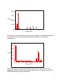
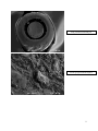
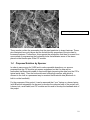
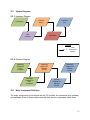
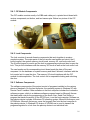
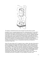
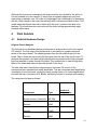
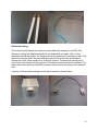
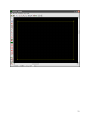
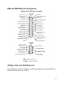
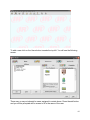
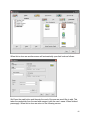
Vanderbilt Locknetics Upgrade
Sponsor: Vanderbilt University School of Engineering (VUSE)
VUSE Senior Design Project
April 22, 2009
Justin Gilstrap
Akin Olugbade
Lutalo Webb
Table of Contents
1 Introduction…………………………………………………………………………….3
1.1 Project Sponsor …………………………………………………………...…... 3
1.2 Executive Summary……………………………………………………..………4
1.3 Project Overview...........................................................................................5
1.3.1 Material Analysis of Banana Pins..………………………………………10
2 System Overview and Description………………………………………………..11
2.1 Background Information………………………………………………………….11
2.1.1 Lock Features………………………………………………………………11
2.2 System Requirements…………………………………………………………12
2.2.1 Hardware Requirements………………………………………………….13
2.2.2 Software Requirements…………………………………………………..13
2.3 System Diagrams………………………………………………………………15
2.3.1 Hardware Diagram………………………………………………………...15
2.3.2 Software Diagram………………………………………………………….15
2.4 Major Component Definition…………………………………………………15
2.4.1 CIP Components…………………………………………………………..16
2.4.2 Lock Components…………………………………………………………16
2.4.3 Software Components…………………………………………………….16
2.5 Current Interface Definition…………………………………………………..17
2.5.1 Card Reader to Host Computer………………………………………….17
2.5.2 Host Computer to Palmtop……………………………………………….17
2.5.3 Palmtop to CIP Module…………………………………………………...17
2.5.4 Host Computer to CIP Module…………………………………………...17
2.5.5 CIP Module to Lock………………………………………………………..17
2.6 Operational Concept…………..………………………………………………17
2.6.1 Operational Diagram………..…………………………………………….18
3 Proposed Solutions…………………...…….………………………………………18
3.1 Wireless RS 232 Connection……...…………………………………………19
3.1.1 Bluetooth……………………………..…………………………………….20
3.1.2 Infrared………………………………….………………………………….20
3.1.3 RF Transmission………………………………………………………..…21
3.2 Zero Insertion Force Pins………………………….…………………………...23
3.3 Re-designing Locks…………………………………….……………………….24
4 Final Solution…………………………………………………………………………24
4.1 Detailed Hardware Design……………………………………………………24
4.2 Detailed Software Overview………………………………………………….30
4.3 System Diagrams………………………………………………………………34
5 Testing…………………………………………………………………………………38
6 Conclusions…………………………………………………………………………...40
7 Suggestions for Future Work………………………………………………………40
8 Appendix…….…………………………………………………………………………42
2
1
Introduction
1.1
Project Sponsor
The Vanderbilt University School of Engineering (VUSE) is sponsoring this project.
Lewis Saettel, a manager of VUSE, is in charge of programming the locks so that
appropriate faculty, staff and students can access rooms within Featheringhill and
Jacobs Hall.
1.2
Executive Summary
Locknetics (Ingersoll Rand/Schlage) locks secure most areas of Featheringhill and
Jacobs Hall. The Computer Interface Programming (CIP) module is the device that is
used to program the door. Lewis Saettel, our project sponsor, and manager of facilities
at Vanderbilt University School of Engineering uses this module daily to grant (or
remove) students and faculty access to the doors in the engineering building. Because
the locks are reprogrammed on a frequent basis, the programming hardware
subsequently suffers damage over time. After multiple uses, the pins of the CIP module
break, or begin to break in such a way that they are no longer useable. About four new
modules are purchased yearly, totaling over $1000 of programming equipment
purchases.
Various issues were encountered as problems with the existing system. The banana
pins of the CIP module are unable to withstand stress of the CIP module and bulky
cable hanging from the module. An additional source of stress arises from the banana
pins being the same length, but the banana pin slots being inconsistent in depths. This
requires the user programming the locks to have to maneuver the module in a manner
that adds stress to the pins. In addition to the stress issues, common occurrences are
electrical connection problems between the CIP module and the lock due to the poor fit
of the pins. In many cases, this requires multiple attempts to program the locks.
These problems have made it necessary to produce a method for programming the
locks that will alleviate the hassle of frequently reordering CIP modules due to broken
pins and save money. The final solution that was implemented an entirely new design
for the CIP module. Circuit analysis was performed which consisted of tracing the
original circuit inside the CIP module using a high magnification microscope and lamp.
The components and their values were identified and ordered. Next, a PSpice
schematic of the existing circuit was formulated and the design was tested for its
functionality on an electric breadboard. Finally, a printed circuit board was ordered and
soldered. New casing, wiring, and pin handles were also created with the assistance of
a machine shop. The new model allowed for the depth of the banana pins to be
3
customized to fit each lock to reduce stress and increase electrical contact. It also
allowed for the banana pins to be unscrewed via the pin handles for easy replacement.
Furthermore, easy access to the module inside of the aluminum casing was ensured for
convenient replacement, if needed. As stated by our project sponsor, an average of
four of the old CIP modules were ordered per year in the past. Aside from the time and
effort required to fix or reorder damage pins, with each model costing $250 dollars, the
cost of ordering new CIP modules over a 5 year period totaled over $5000. The new
and improved design costs $28.76 per unit to construct. If four were needed to be
ordered each year, $4424.80 will be saved by Vanderbilt University School of
Engineering over a five year period.
Potential further steps in this project include additional research on wireless
communication. Possibly Bluetooth or infrared technology could be used to wireless
program the locks. The locks in the engineering building are offline so programming
would still have to be done door by door, however, a small device could be attached to
the lock in order to transmit programming data from a handheld PC to the lock circuitry.
Additionally, a more compact design that would cut down on wire length as well as
module size could be implemented.
1.3
Project Overview
Locknetics (Ingersoll Rand/Schlage) locks secure most areas of Featheringhill and
Jacobs Hall. There are over one hundred doors that use these particular locks
throughout Featheringhill and Jacobs Hall. The locks are considered “stand alone,”
meaning there is no central point that connects or wires them. Therefore, they are
powered by four industrial type AA batteries and one 3 volt button battery for memory
and date and time backup. The locks are designed with security as the utmost priority,
and with practicality as its second.
A database software program, which is based on Microsoft Access tracks and controls
the programming of the doors. A small program called UPLINK.EXE is used to bring
the programming data of a lock(s) from the host computer to an individual lock. A
handheld PC uses Microsoft Activesync to sync the program files from the host
computer to the handheld. The handheld has a Windows CE version of the
UPLINK.EXE software that allows one to carry the small handheld unit around to
program the individual locks. Locks are re-programmed on a daily basis and
subsequently the handheld and its programming hardware suffer damage over time.
The programming hardware includes a USB/Serial to Hewlett Packard handheld cable
and a programming module called a Computer Interface Programmer (CIP). The CIP
module is used to program the door and to read the ibutton credential. After multiple
uses, the pins of the CIP module break, or begin to break in such a way that they are no
longer useable. The pins on the CIP module that touch the lock are miniature banana
pins. Once the pins break, a new CIP module must be purchased. The cost of a CIP
module is approximately $200.00 to $275.00 each. The order time for a CIP can be
months since IR Locknetics offers no support for end users. One must go to a lock
4
company that is authorized to order parts for these locks in order to get spare parts.
The ability to program locks is only plausible when there is a CIP module.
Due to this problem of the miniature banana pins constantly breaking, causing the need
for more CIP modules, it is necessary to produce a method of programming locks that
will alleviate the burden of frequently re-ordering CIP modules and limiting the number
of broken pins.
1.3.1 Material Analysis of Banana Pins
One of the challenges that need to be addressed with the future solution is that of the
feeble banana pins. The miniature banana pins on the CIP module must be placed into
the lock to be programmed. After multiple uses, the pins begin to break due to the
weight of the CIP module attached to the handheld PC. A scanning electron microscope
and Energy-Dispersive X-Ray Spectroscopy were used to get a better understanding of
the effects of stress on the pins and the material makeup of the pins. Pins in various
states were studied. A pin that had been exposed to no stress was studied, a pin that
was worn and beginning to break was studied, and a pin that had suffered a fracture
from excessive use was studied. The pictures below show a CIP module with pins that
have not been used.
The following EDS Spectra diagram shows the material makeup of the outside layer of
the banana pins. Based on the diagram, it has been concluded that the pins are gold
plated.
5
4000
Au
3000
Counts
2000
1000
Au
Au
Ni Au Au
0
5
Au
Au
Au
Au
10
Energy (keV)
15
Next, the core of the outer section of the pins was analyzed. It was determined that the
core of the outer section was primarily a copper nickel alloy for solid solution
strengthening.
500
Cu
400
Cu
300
Counts
200
Ni
100
Cu
0
2
4
6
Energy (keV)
8
Finally, the middle core of the pin, where full fractures occur, were tested. It was
determined that there were traces of copper, lead, and zinc to form a brass core. The
EDS Spectra diagram can be seen below.
6
Counts
1000
Cu
800
600
Cu
400
200
Cu
Pb
Zn
Pb
PbPb
Ni
0
0
5
Cu
Pb
10
Energy (keV)
Pb
Pb
Pb
Pb
15
The next form of material analysis involved the use of the scanning electron
microscope. The following magnified images clearly show the state of the pins before
being worn down, while being worn down, and after being broken.
Image of banana pin that has not
been previously used
7
Image of banana pin that has been
worn out and the outer casing has
broken
Image of worn banana pin zoomed
in on fracture of outer casing
8
Fully fractured banana pin
Close up of fractured surface
9
Close up of fractured surface
These results confirm the assumption that the pins break due to stress fractures. These
pins illustrated low cycle fatigue and the limited ductility properties of the pins lead to
increased fractures. Furthermore, this supports the assumption that there is a need for a
new method of programming the Locknetics locks that alleviates some of the stress
placed on the banana pins of the CIP module.
1.4
Proposed Solution by Sponsor
In order to save money for VUSE and to reduce possible downtime, our sponsor
proposed that the CIP module get reverse engineered so that it’s data can be
transmitted via Bluetooth instead of direct serial data (assuming the data from the CIP is
typical serial data). Then the lock would need a Bluetooth receiver with which to
connect to the lock in a permanent way to received the Bluetooth data (Bluetooth is
built-in on the handheld)
For the purposes of this project, it can be assumed that “your” laptop or a loaner laptop
(with Bluetooth integrated) can be used to develop the computer side of the project and
a loaner lock, serial cable, and CIP module can be used to develop the hardware side of
the project.
10
2
System Overview and Description
2.1
Background Information
2.1.1 Lock Features
The lock consists of both hardware and software components. The features of the
hardware are listed below:
Built on proven, industry-leading heavy duty, ANSI Grade 1, Schlage lock
platform
Stand-alone electronic locking system - no hardwiring required
Open track 1 or 3 encoding allows the key card to carry access changes to doors
limiting the need to reprogram locks!
Magnetic Stripe card reader with metal 6 or 12 button PIN pad
Manages unlimited number of cards
Complete history of last 1000 door events, including authorized entry and
unauthorized access attempts
High-security mechanical key override (Schlage Everest cylinder)
Detects and stores event when an emergency override key is used
Privacy override available on specifically designated cards
60,000 to 80,000 cycles for minimal routine maintenance, utilizing four 4 standard
AA batteries
Available in cylindrical and mortise locks and exit device trim for the Von Duprin
98/99 series devices
Available in a variety of finishes and lever styles
Vandlgard® clutching lever design
Batteries and electronics are positioned on the secure side of door
The features of the software of the locks are listed below:
Integrates with all levels of security - from brass keys to biometrics
User friendly/intuitive software for day to day operations
Integrates the Ingersoll-Rand online and offline access control systems,
eliminating the need and inefficiency of having two separate databases
Manages an unlimited number of unique PIN codes, where card and PIN is
required for access
Single and multiple workstations (with client server) can be easily networked to
conveniently access a single database
Ability to specify gender and ADA when encoding cards
Easily integrates with other campus databases
Interfaces with leading “One Card” providers
11
2.2
System Requirements
The system requirements are seen in the table below.
I.D. Number
Requirement
1.0
System shall fulfill all hardware specifications.
2.0
System shall fulfill all software specifications.
3.0
System shall not conflict with pre-existing operational concept.
4.0
System shall not require more than two trials to update lock.
5.0
System shall detect electrical contact within five seconds of banana
pin insertion into lock.
6.0
System shall reduce the number of broken banana pins from
programming by fifty percent.
7.0
System should cost 30 percent less than the existing system.
The first two requirements relate to the hardware and software specifications. These are
vague, but explained in detail later. Requirement 3.0 is needed to ensure the project
sponsor can still easily use the new system with no additional training. This essentially
eliminates any transitional period between use of the old and new system to program
the locks. Because the previous system was unreliable in the number of trials needed to
program the locks, Requirement 4.0 was added to make certain the new system
effectively increased the success rate of programming locks. At times, the Locknetics
program would report that no data was being transmitted to it and this was commonly
due to poor electrical contact from the banana pins. Requirement 5.0 was added to
guarantee the electrical contact of our new system is actually an improvement.
Requirement 6.0 addresses the major concern of the project. The existing system
required banana pins to be replaced or repaired more than eight times in a school year.
Therefore, Requirement 6.0 to ensure the new system is in fact reducing the stress
placed on the banana pins which causes them to break so frequently. Lastly,
Requirement 7.0 was added as an incentive to make the new system more cost
effective. The project sponsor did not demand this requirement be fulfilled (hence, the
12
“should” statement), but it would be beneficial to both the sponsor and the school of
engineering for the cost of the new system to be less than the existing system.
2.2.1 Hardware Requirements
Since Requirement 1.0 was vague in its explanation of hardware specifications,
Requirements 1.1-1.7 were added to better describe the hardware requirement. The
table below shows these requirements.
I.D.
Number
Requirement
1.1
Host Computer shall process changes and stores database of access rules
1.2
Host Computer shall have standard keyboard, monitor, etc.
1.3
Card Reader shall acquire user information from cards for use to update
database on host computer
1.4
Palmtop Device shall store updated database while going from lock to lock
1.5
Transmission Medium shall send updated card access rules from the Host
Computer to the Palmtop Device
1.6
Transmission Medium shall send the updated card access rules from the
Palmtop Device to the Lock Interfacing Module
1.7
Lock Interfacing Module shall accept new data and places it in the lock
2.2.2 Software Requirements
Since Requirement 2.0 was vague in its explanation of software specifications,
Requirements 2.1-2.8 were added to better describe the software requirement. The
table below shows these requirements.
13
I.D. Number
2.1
Requirement
Operating System for Host Computer shall enable control of the host
computer
2.2
Database Program shall store and organize the card access rule for
each lock
2.3
Database Program shall keep an inventory of all the users that have
access to locks
2.4
Palmtop Synchronization Software shall synchronize the database on
the Palmtop Device with the database on the Host Computer
2.5
Palmtop Synchronization Software shall package and send data to
the IO Ports on the computer
2.6
Palmtop Operating System shall enable control of the Palmtop Device
2.7
Palmtop Database Software shall organize and store the card access
rules on the palmtop device
2.8
Lock Synchronization Software shall package and send information to
IO ports of the Palmtop device intended for the lock
14
2.3
System Diagrams
2.3.1 Hardware Diagram
Palmtop
Device
Card Reader
Host
Computer
Locknetics
Lock
CIP Module
Legend
=
Data
Transmission
Medium
2.3.2 Software Diagram
Operating
System for
Host
Computer
Operating
System for
Palmtop
Device
Database
Program on
Host
Computer
2.4
Uploading
Program on
Palmtop
Device
Syncing
Program on
Palmtop
Device
Major Component Definition
The major components of our project are the CIP module, the Locknetics lock, software,
and hardware. Each of these components also has various components within them.
15
2.4.1 CIP Module Components
The CIP module consists mostly of a DB9 male cable port, a printed circuit board with
various components, an ibutton, and two banana pins. Below is a picture of the CIP
module.
2.4.2 Lock Components
The lock consists of several discrete components that work together to create a
complete system. The major parts of the lock are the card reader and circuit, the 6
button keypad, the system memory circuit board, memory I/O, and lock control unit.
The 6 button keypad is used to put the lock in programming mode and also to open the
lock. This pin thus interfaces with the memory I/O circuit as well as the lock control unit.
The card reader and its corresponding circuit board reads the data off the card,
compares it to the database on system memory and then if allowed, interfaces with the
lock control unit to open the door. The memory I/O circuit interfaces with the CIP
module for data acquisition. The lock control unit is responsible locking and unlocking
the door.
2.4.3 Software Components
The software components of the project consist of programs installed on the various
pieces of hardware. On the host computer, the operating system is Windows XP with
Service Pack 3 installed. Other software on the host computer includes the Locknetics
software program, which is a database software program based on Microsoft Access
that tracks and controls the programming of the doors. Also, Serial Port Sniffer, a
program that tracks the activity of the RS 232 port, is on the host computer. Software on
the palmtop device includes a Windows CE operating system, Microsoft Activesync, and
UPLINK.exe. Microsoft Activesync syncs the program files from the host computer to
the palmtop device. A Windows CE version of UPLINK.exe is used to transmit the
programming data for a lock from the palmtop device to an individual lock.
16
2.5
Current Interface Definition
2.5.1 Card Reader to Host Computer
The computer interfaces with card reader via a USB cable. The card reader is used so
that manually typing in of the user’s social security number and name is not needed.
The cable used is a standard USB 2.0 cable that comes from the card reader and
connects to the USB port of the host computer.
2.5.2 Host Computer to Palmtop
The host computer connects with the palmtop device by a custom USB cable. This is
standard connection for most palmtop devices. The computer end of the USB cable is a
standard size USB interface. The palmtop end of the USB cable is custom serial
connection. Conversion from this custom styled serial port to USB occurs inside the
cable and full compatibility is maintained. As fitting with the USB standard,
communication is serial.
2.5.3 Palmtop to CIP Module
The palmtop device interfaces with the CIP module via a custom RS-232 cable. As the
palmtop devices serial port is not standard, a specialized cable is used to connect to the
CIP module. This cable converts the wiring from the custom port to standard RS-232.
The standard end of the cable is an RS-232 9 pin female. The CIP Module has a 9 pin
male connector to which plugs into the female RS-232 port. As fitting with the RS-232
standard, communication is serial.
2.5.4 Host Computer to CIP Module
At some times, it may be necessary to interface a host computer directly with the CIP
module. This is the case during testing with a laptop. This case requires a specific RS232 cable. This cable fits in the serial port of the computer and has a female connection.
The CIP module end of the cable also has a female 9 pin port and plugs into the 9pin
male RS-232 connection on the CIP module. Communication is serial.
2.5.5 CIP Module to Lock
The CIP module interfaces with the lock via two pins. These pins send data from the
CIP module to the lock by direct pin connection into two sockets of the lock.
Communication is serial.
2.6
Operational Concept
The operational concept is not the most difficult, but can be quite tedious. First, an
individual (faculty, staff, or student) request access to room in Featheringhill or Jacobs
Hall. Once approved, the Vanderbilt card of the individual is then swiped through a card
17
reader, which transmits credentials data of the individual to the host computer through a
transmission medium (i.e. USB cord). The data on the host computer is transferred to a
database program within the host computer. That data is transferred to a palmtop
device through a transmission medium. From the palmtop device the data is uploaded
onto a syncing program on the palmtop. An uploading program is then needed to enable
data transfer from the palmtop to the CIP module. Using this program, the data is sent
to the CIP module through a transmission medium. The lock is then placed in
“programming mode” via the keypad or a card swipe. Data is received by the lock by
way of two pins on the CIP module placed in contact with the lock. Once the lock
receives the data, the individual’s Vanderbilt card is swiped through the card reader on
the lock to verify whether lock was properly programmed. The lock light blinks green if
access to the individual is granted, thus the lock was programmed successfully. If
unsuccessful, the lock light blinks red and the process repeats until the lock is
successfully programmed. Below is the figure that displays the operational concept in a
block diagram.
2.6.1 Operational Diagram
3
Possible Solutions
It was made clear by our sponsor that it is preferred that the project entail a re-designing
of the CIP module to make use of wireless connection; however, it is still important to
confirm all other possible solutions are explored to assure the most effective and most
cost-efficient method is selected.
18
3.1
Wireless RS 232 Connection
The RS-232 standard, also known as EIA 232, is a communication standard for serial
binary communication between two devices. One of these devices is Data Terminal
Equipment and the other is the Data Circuit-terminating Equipment. These are
abbreviated as DTE and DCE respectively. RS-232 voltage levels for representing
binary information is different than that for CMOS or TTL logic. A binary “1” is
represented by a negative voltage and logic “0” is represented by a positive voltage.
Voltage levels near zero are invalid. Acceptable voltage levels are f plus or minus 3 to
15 volts. This wide voltage range compared to typical integrated circuits necessitates
the need for logic conversion circuits when interfacing the two.
There are standard cables and ports associated with the RS-232 standard. The most
common cables forms are the 25 pin and 9 pin versions. Each pin on a connecter has a
specific function and this function is standard for 25 and 9 pin male/female connectors.
An example RS-232 linked system can be seen below. Details of pin assignments for
the standard cables can be seen in the appendix.
The current lock programming system incorporates RS-232 into its design. Data is
transferred to the CIP module via a cable that conforms with the RS-232 standard. Data
transfer can happen using a computer’s or palmtop’s RS-232 serial port to the RS-232
port that exists on the CIP module. This allows us to confront the breakage problem by
considering several options that involve eliminating the cable between the transmitting
device and the CIP module. The general premise is to encode the RS-232 data coming
from the transmitting device into a wireless standard and then decode that data back to
RS-232 at the CIP module. Eliminating the cable would reduce much the rest stress
placed on the pins of the CIP module by eliminating the stress caused by the cable on
the CIP module. Next we will discuss the possible standards which we could use to
implement wireless RS-232.
19
3.1.1 Bluetooth
Another possible solution to the problem was to implment the transmission of data from
the data host to the lock via bluetooth. Bluetooth was actually actually conceived as a
wireless RS-232 solution. It is a lower power, medium range, wireless communication
protocol that has gained popularity over the years. There are currently three classes of
bluetooth with class 3 having the shortest range and consuming the lowest power, and
class 1 having the longest range and consuming the most power. These are seen
below.
Class
Maximum Permitted Power
mW (dBm)
Range
(approximate)
Class 1
100 mW (20 dBm)
~100 meters
Class 2
2.5 mW (4 dBm)
~10 meters
Class 3
1 mW (0 dBm)
~1 meter
Class three Bluetooth is what is used in cellular phone headsets that implement
Blutetooth. Considering the proximity that a person updating a lock would be, class
three would work well. It consumes the least amount of power and thus saves on
energy spent.
There are multiple ways that one could go about implementing via Bluetooh. If the
palmtop device that is used to uplink data to the lock has a Bluetooth interface, which
ours does, one could transmit data directly from the palmtop to the a Bluetooth to RS232 module. This, however, would require reverse engineering the proprietary software
which is used to send data from the database on the palmtop to the lock. While,
theoretically possible, it would require advanced software skills and would possibly be
illegal.
Another option would be to use a RS-232 to Bluetooth transmission module at the
palmtop device and then an Bluetooth to RS-232 receiver module at the CIP module.
Many stand alone RS-232/Bluetooth conversion pairs exists and can be found and
purchased failry easily.
3.1.2 Infrared
The use of the infrared portion of the electromagnetic spectrum for communication is
very common. Most remote controls use it to control TVs, DVDs, and other electronic
devices. It has also become popular on palmtops devices, including ours. For this
20
reason we could once again, attempt to reverse engineering the software that is used to
send data serially. The goal in this case would to purchase an infrared to RS-232
receiver module and configure the software on the palmtop such that data is sent via
the infrared port instead of the serial port. The problem with this approach remains the
fact that reverse engineering proprietary software would be extremely difficult and
possibly illegal.
Another option would be to use a RS-232 to infrared transmission module at the
palmtop device and then an infrared to RS-232 receiver module at the CIP module.
While not as prevelant as the modules for bluetooth, one can find the needed
components for sale. They are, however, generally cheaper than bluetooth devices of
similar kind.
3.1.3 Radio-Frequency Transmission
Yet another solution for wireless data transfer between the CIP module and the lock
was to use the radio spectrum to send data. Radio Frequency (RF) transmission is
common in several communication applications. Using this approach, one would have
to purchase a RS-232/RF conversion modules as the palmtop does not have an RF
transmitter, receiver, or transceiver. However, RS-232/RF transmission modules are
extremely prevelant and extremely cheap. RF is generally low power while still
providing a large range. In addition, typical RS-232 transmission rates are not as high
as what is provided by Bluetooth or infrared. As, such, RF would not provide excess,
uneeded bandwidth.
3.2
Zero Insertion Force Pins
Another potential solution was the incorporation of zero insertion force pins. This would
prevent the pins from breaking due to excessive force. Zero insertion force, a concept
used in the design of IC sockets, was invented to avoid problems caused by applying
force upon insertion and extraction. After extensive searching, it does not appear that
zero insertion force pins will be able to be found for use with our project. The closest
application found was that of a zero insertion force compliant pin contact and assembly
seen below. It describes a compliant pin contact and assembly in which the contact is
comprised of two layers, each of a different material and coefficient of thermal
expansion (CTE) than the other, to enable insertion within an opening in either a “cold”
or “hot” state to thereby expand and positively engage the opening's walls, thereby
securely holding the pin in position. Representative materials include Invar and
aluminum.
21
The majority of information found on zero insertion force pins was for use with
integrated circuits. A normal integrated circuit (IC) socket requires the IC to be pushed
into sprung contacts which then grip by friction. For an IC with hundreds of pins, the
total insertion force can be very large (tens of newtons), leading to a danger of damage
to the device or the PCB. Also even with relatively small pin counts each extraction is
fairly awkward and carries a significant risk of bending pins (particularly if the person
performing the extraction hasn't had much practice or the board is crowded), as can be
seen with the unpopular front-loading mechanism of the Nintendo Entertainment
System. Low insertion force (LIF) sockets reduce the issues of insertion and extraction
but the lower the insertion force of a conventional socket, the less reliable the
connection is likely to be.
With a ZIF socket, before the IC is inserted, a lever or slider on the side of the socket is
moved, pushing all the sprung contacts apart so that the IC can be inserted with very
little force (generally the weight of the IC itself is sufficient with no external downward
force required). The lever is then moved back, allowing the contacts to close and grip
the pins of the IC. ZIF sockets are much more expensive than standard IC sockets and
also tend to take up a larger board area. Such a technique has disadvantages that the
connector will occupy a large volume since it adds the space of the drawbars and the
slide-able space thereof. Therefore, the technique is not useful in the future
development of the chips with a high density and large number of pins. Further, the
connecting construction of the patent is not good enough to provide a close
22
engagement between the pins and the drawbars. There are only two engagement
points between the pins and the drawbars which will probably result in a poor
connection in a short time. Also they are known to bend the IC pins at times. Therefore
they are only used when there is a good reason to do so.
Large ZIF sockets are commonly mounted on PC motherboards (from about the mid
1990s forward). These CPU sockets are designed to support a particular range of
CPUs, allowing computer retailers and consumers to assemble motherboard/CPU
combinations based on individual budget and requirements. CPUs may also be
upgraded or replaced during the lifetime of the motherboard socket. Personal
computers are among the few applications expensive enough to justify elaborate socket
systems. Smaller ZIF sockets are also commonly used in chip-testing and programming
equipment.
3.3
Re-designing Locks
An additional solution suggestion was to redesign the circuitry within the lock so that no
pins would be required to program each lock. This would mean implementing a mini
wireless CIP module and installing this on the inside of each lock. This way, there would
be a direct connection from the mini CIP module to the back side of the two pins on the
locks. Once the lock was put into programming mode, it could be reprogrammed without
the insertion of pins.
Mini CIP module would be placed within the lock above
23
Although the outcome of redesigning the locks would be very desirable, this option is
not very feasible for a few reasons. It would it be an extreme hassle and very time
consuming to redesign over 100 locks in Featheringhill Hall. Additionally, by tampering
with the circuit design in the locks, the warranty with Locknetics would be broken. This
would mean that if there was ever a defect with the lock, it would not be able to be
replaced. This could become very costly with the locks costing approximately eight
hundred dollars each.
4
Final Solution
4.1
Detailed Hardware Design
Original Circuit Analysis
The first step in our hardware design process was to analyze the circuit in the original
CIP module. The first step in this process was to accurately do a paper and pencil
sketch of the circuit board. The challenge came from the two sided property of the
board. That is, there are traces on both the bottom and the top of the circuit board. To
deal with this problem, we used a high magnification microscope with a high powered
light that was able to shine through the board. This enabled one to view through both
sides of the board and make an accurate sketch of the circuit.
The next step was to identify the components on the board. All but one of the
components were standard and easily identifiable. The last component was identified by
unsoldering it from the board, viewing the party number listed on it under magnification,
and with the help of professor A.B. Bonds, identifying the part in an electronics catalog.
The component list was as follows:
Component
Type
Number of
Components
Bipolar Junction Transistor
2N 3904
2
Resistor
22kΩ
1
Resistor
2.2kΩ
2
Resistor
10kΩ
2
24
Resistor
120Ω
1
Diode
1N4148
3
Diode
1N5232
1
Capacitor
10μF
1
Circuit Simulation
The next step in the design process was to simulate the circuit which was sketched. To
do this PSpice was used to layout our sketched circuit as a PSpice schematic.
The circuit was then simulated by applying a several inputs to both the RS-232 and twopin side of it. There were 4 pins on the RS-232 side that could be asserted or
unasserted. Thus there were 16 combinations of inputs to apply to it on the RS-232
side.
This was done and it was noted that the output on the lock interfacing side was either
close to 0v or close 5v. This enabled us to determine that the output was not some form
of RS-232 and was instead closer to the logic levels used in many common electronics
(TTL). This is significant because we originally believed that the CIP module still
communicated with the lock using RS-232 levels and hoped that this would allow us to
use a wireless RS-232 standard. We rejalized that since the lock was using TTL logic
levels, we could not do this.
An example of the circuit simulation is given below:
25
Breadboarding
Once the simulation was completed, the next step was to demonstrate that the circuit
that we simulated was indeed correct and would work as expected. This was done
through the process of breadboarding. We laid out a version of the circuit on a
breadboard with inputs being interfaced with the lock and the RS-232 cable. An
updating process of a lock was then done through the breadboard to verify the validity
of the circuit.
PCB Design
The next step was to design the circuit for custom fabrication. This was done using
software called ExpressPCB. ExpressPCB had a large component library that helped
not only because of its size but also because the components were scaled to size. That
is, they took up the same relative size in the software layout as they would on the
physical PCB.
We started at the default PCB size of 3.8x2.5 inches. This made it easy to simply layout
the circuit without confusion or errors. As on the original CIP module circuit, we placed
traces on both sides of the board. This is done when traces would otherwise cross
26
each other and it helps avoid making very convoluted. Once this was done, we went
through two additional iterations in order to shrink the size of the PCB down to a
reasonable size.
Pictures of the iterations and the final design are shown below.
3.8x 2.5 in.
1.8x1.725 in
1.475x1.4 in.
After we designed the PCB, it was relatively simply to order it due to the integration of
the ordering process with the software. Forms were filled out regarding shipping, billing,
quantity, and board type. After the this was all determined the design file was sent
directly to the ExpressPCB servers. An example of an ordering form is shown below.
27
When we received the board we immediately noted a design error. Our inexperience
with designing PCBs caused confusion with the nature of two sided boards. As such a
trace came in contact with a through-hole that it was not intended to touch. This made
the boards ordered invalid. A picture of a zoomed in portion of the board with the error is
shown below. The error is in the white box.
This error was corrected by simply moving the trace upwards slightly so that it no longer
came in contact with the through-hole.
PCB Construction
Once the board was received we began the process of constructing it. Using the design
file as a guide, we soldered the components in their respective places. We used rosin
core solder. This has flux in the core of the solder and makes better solder joints. In
addition to the components, we placed a male DE9 connector that was previously
ordered on the board. We soldered the pins to the pin holes to complete the DE9
connection. Lastly, we soldered two 18 gauge wires to wire holes meant to interface
with the lock.
28
A picture of the constructed PCB is shown below.
Pin Handles and Wiring
We enlisted the machine shop associated with the Vanderbilt Physics Department to
help us with several parts of our final hardware design. The first of these parts was the
custom handles that we now have. One problem that the design of the original is that
pins were fixed in relation to one another. This coupled with the fact that the holes with
which the pins interface were not leveled but the pins were led to extra stress being
placed on the pins when trying to make a good electrical contact.
In order to combat this problem we wanted to make the interface with the lock as free as
possible. To accomplish this we made the pins connected to handles which were in
turn connected to two separate wires. This allowed for a great deal of freedom.
The pin handles themselves were custom made at the machine shop. They were
molded from plastic and made to fit our banana pins in terms of threading and pin
diameter. The pins are simply screwed into the handles due to the custom threading
inside of the handles.
The pins had holes drilled into them bottom of them. The 18 gauge wire was placed in
these holes. The pins were heated up with a high power soldering iron and rosin core
solder was placed in the pin hole with the wire and melted to the exposed copper wire
that composed the wire. This wire was then run through the pin handle and the pin was
screwed into the handle. This made electrical connection with the pin/pin handle and the
wire.
The wires that extended from the pins were connected on the other end to the PCB. To
make a cleaner design we put the two individual wires inside a heat shrink tubing. The
heat shrink tubing was made to shrink using a novel idea of a paint stripping tool.
Pictures of the pin handles and wiring are shown below.
29
Aluminum Casing
The machine shop helped us develop a custom aluminum casing for our PCB. The
Aluminum casing was fitted specifically for our board and our needs. Some of the
requirements that we had for our design was that the case must be strong and light. The
aluminum casing is both. We also wanted to ensure that in the case we needed to
access the circuit, there would not be a difficult process. The aluminum casing has a
cover that is secured by only four screws. This makes it secure as well as modular. The
casing also had a space for the DE9 connector and a hole for the wires on the opposite
side.
A picture of the aluminum casing and the whole system is shown below.
30
4.2
Detailed Software Overview
Overview
The primary programs used during our project were PSpice, LockLink, and
ExpressPCB. PSpice was used for constructing circuit schematics and simulation of
circuits. LockLink was used to manage card access rules, and Express PCB was used
to design and order our custom PCB.
PSpice
PSpice (Personal Simulation Program with Integrated Circuit Emphasis) is an analog
circuit and digital Logic simulation software. It can be used for simply generating circuit
schematics but its main use is reliably simulating integrated circuits before going
through the expensive manufacturing process. Integrated circuits, unlike circuits
composed of discrete components cannot be breadboarded before actual manufacture.
As such SPICE programs are used as a way to test them virtually before going through
the expensive photolithography process.
In our project, we used PSpice to make an important discovery which determined the
trajectory of our project significantly. We used PSpice to create a schematic of the CIP
circuit and simulate it. PSpice has a large library of common components. We were able
to identify all the components in the CIP circuit and construct it in PSPice. PSpice
enabled us to perform extensive simulations to the circuit and determine the expected
behavior of the circuit. This enabled us to determine that the CIP circuit converted RS232 logic levels to 5v/0v logic levels and vice versa.
LockLink
LockLink is an access control management software developed by Ingersoll Rand
meant to be used with their with their Locknetics Lock system. It manages all the locks
in the system, the users in the system, and the access rules.
The LockLink software allows for the mapping of multiple facilities, each which may
have multiple buildings. The buildings in the facilities may (and typically do) have
multiple doors.
The management of users in Lock Link is extremely robust. In the basic use, one can
add a user and set an array of access privileges and credentialing. Each user can have
more than one method of credentialing (Magnetic Card, Keypad, iButton, etc.) as well
as a specific kind of access. This can be normal access, or special privileges such as
the ability to access a lock even in the case of a lockdown of a building.
To simplify the process of setting user access rules LockLink supports user groups. This
is useful in situations when a certain set of users will have the same access privileges to
a large number of doors. One first sets the rules for that user group and then any user
who must be added to the system who fits the profile for a user group can simply be
added to that user group and the access rules will automatically be applied. After being
31
added to a user group, a user can still gain additional access rules by having them
added manually.
LockLink also can set rules to individual locks themselves. This includes the “smart
time” function which can dictate how the lock works depending on the time of day. This
can enable locks to be unlocked for a certain time of day and then only allow card
access for a certain time of day.
The last major function of the LockLink software is the ability to interface directly with
the locks in order to send access rules to the locks as well as well receive access logs
from the locks. This was a function that we used repeatedly when testing our circuit. We
used the uplink function to send card access rules to the lock to ensure communication
was working correctly. We also were able to read the credentials from cards into our
database by swiping a card through the lock. These two combined showed that we were
interfacing in a bidirectional manner.
The version of the software we used during our project was 7.3.5.
ExpressPCB
ExpressPCB is the free software that we used to layout our custom PCB. The software
allowed for the layout and easy ordering of custom PCBs. The software enabled double
sided PCBs as well as ground and power planes.
A very useful property of the software was its large collection of common components
that when placed on the layout represented their size accurately. This helped one
placing traces on the board as size considerations are extremely important when
making a PCB.
Lastly, the ordering service was integrated into the software. When ready to order, one
can determine the board type, quality, and quantity. The shipping and billing information
is entered and the design file is then sent directly to the ExpressPCB servers.
A screen shot of the software is below.
32
33
4.3 System Diagrams
External Lock Makeup
The diagram above shows the external components of the Ingersoll Rand locks. The
card swipe is the main component used for gaining access to rooms in Featheringhill
and Jacobs Hall. We used this component of the lock to verify whether the CIP module
successfully updated credentials to the lock interface and Locklink software. The LED
lights indicate whether card access, iButton access, or keypad code entry was granted
or denied. They also blink and turn different colors depending on the programming
stage on the lock that is being utilized. The iButton slot enables a device referred to as
an iButton to transfer stored information into the lock’s memory. The iButton is a 16
millimeter computer chip encased in a water tight stainless steel container smaller than
a dime. The container is attached to a plastic keyfob designed to fit on a keychain. Each
iButton has a unique ID number which is detected by the lock when the user taps his or
her iButton to it. The iButton is unaffected by magnetic fields, metal detectors, water and
most chemicals. To store information, the iButton is connected into a receptor and
software transfers the lock access data to the iButton. The iButton is then unsnapped
from its receptor and can be touched to each lock. The iButton setup information is
transferred to the lock’s memory. This device is seldom used in the engineering
building. Next, the keylock is the traditional way of opening locks and requires a key for
entry into the room. A master key is provided to the facilities manager and there are
individual keys for each door, however, these are not distributed for use by students or
34
faculty. Moving on, each door has a distinct five digit code that can be inputted onto the
keypad for entry. If the code is incorrect, the LED light flashes red and if it is correct, the
LED light flashes green and unlocks the door for about three seconds. This is the
second most common way that faculty and staff use to gain entry into various rooms
within the engineering building. The pin connectors labeled in the diagram above serve
as the slots for the banana pins of the CIP module to be inserted. They are at different
depths to compensate for the iButton functionality. This depth inconsistency was one of
the problems leading to stress and electrical contact problems between the door and
the lock. The left side of the pin is the negative terminal for the banana pins and the
right side is the positive terminal. Finally, the door knob is the part of the lock that is
rotated downwards for entry into the rooms.
Lock Block Diagram
The lock block diagram above is a general representation of the broad components
needed to reprogram the locks. As can be seen, the card reader, or card swipe
component, connects to the numerical keypad. The keypad circuit connects to lock
circuit located inside the back capsule of the lock. Inside the back of the lock is also, a
source of battery power. The lock is powered by four industrial type AA batteries and
one 3 volt button battery for memory and date/ time backup. The lock circuit is
multilayered, sends out a signal to unlock/lock door, and then the LED lights, which are
a part of the keypad assembly, respond to the signal received. The only component of
the lock block diagram that is not connected to the lock itself is the computer interface
programming module. This module is inserted into the pin connections located on the
keypad assembly and was the main focus of the project. Data is transmitted to the CIP
module via a handheld PC.
35
The pictures below show a “real world” representation of the lock block diagram as
previously discussed.
Front Interior of Lock
Back Interior of Lock
36
“IDF” Model
The system diagram above shows the IDF model (increased degrees of freedom model)
that was implemented as the final solution. In this model, the Palmtop device is
connected to the newly design CIP module with custom aluminum casing via a cable.
Next, the smart cable that consists of two 18 gauge wires is combined via 1/8” heat
shrink tubing. This cable is solder-connected to the banana pins and threaded through
the banana pin handles. As seen in the model above, the pins connect into the pin slots
on the keypad assembly of the lock. This model lowers cost, places less stress on
banana pins, can be implemented in a reasonable amount of time, and is a simple
design as compared to the wireless alternative discussed in the possible solutions
section.
Clamp Attachment Model
The clamp attachment model pictured above is an optional add-on that was created to
program the locks without having to hold the individual banana pins into the slots. On
the back side, there are two screws that allow the model to open for the pins to be
37
clamped in at different depths for a custom, snug fit into the lock. This machine shop
addition provides more stability, is adjustable, improves electrical contact, and is
removable if its use is not desired by the lock programmer.
5
Testing
PCB Design
Prior to ordering the PCB from Express PCB, verification that the circuit design was
correct was needed. To ensure this the circuit was replicated using a breadboard,
wiring, and the same components specified within the PCB design. Wires were soldered
into a DB9 connector/cable to enable testing of the circuit. The process of programming
the lock was then performed and a lock was successfully programmed. This validated
the PCB design layout and allowed the circuit board to be ordered in bulk.
CIP Module Upgrade.
In order to verify the effectiveness and efficiency of our system, fifty attempts were
made to update the lock using the new system. At the start of each trial, the credentials
of a student were read into the database by swiping their Vanderbilt card through the
lock. The user was granted access to the trial lock on the database within the
Locknetics software on the laptop used. Then the new system was used to program the
lock and the card was swiped afterwards to verify the lock was programmed correctly.
The results are seen in the table below.
Trial
Number
1
2
3
4
5
6
7
8
9
10
11
12
13
14
15
16
17
Results
Successful
Successful
Successful
Successful
Successful
Successful
Successful
Successful
Failed
Successful
Successful
Successful
Successful
Successful
Successful
Successful
Failed
38
18
19
20
21
22
23
24
25
26
27
28
29
30
31
32
33
34
35
36
37
38
39
40
41
42
43
44
45
46
47
48
49
50
Successful
Successful
Successful
Successful
Successful
Successful
Successful
Successful
Successful
Successful
Successful
Successful
Successful
Successful
Successful
Successful
Successful
Successful
Successful
Failed
Successful
Successful
Successful
Successful
Successful
Successful
Failed
Successful
Successful
Successful
Successful
Successful
Successful
Trials were successful if the lock light blinked green when the card was swiped after
programming the lock. Trials were unsuccessful if the lock light blinked red when the
card was swiped after programming the lock. This was mainly due to poor electrical
contact from the banana pins when programming the lock. Notification of this was seen
through the Locknetics program alerting the user that the lock was not properly updated.
Of the fifty trials, four trials failed and resulted in an unsuccessfully programmed lock.
Therefore, 92% of the trials were successful, which is a significant improvement from
the previous system as described by the project sponsor.
39
6
Conclusions
There were three goals for this project: (1) to minimize the amount of stress on the
banana pins when programming the lock module; (2) to increase the electrical contact
between the banana pins and the lock when programming the lock with the CIP module;
and (3) to reduce the price of the CIP module. All of these were successfully completely
by then end of the project. The new system allowed for the minimizing of stress on the
banana pins by increasing the degrees of freedom through allowing pins to move
independently of one another. The new system increases the electrical contact between
the banana pins firstly by allowing each pin to adjust the depth at which it is inserted into
the lock and secondly by the additional clamp that increases the stability of the pins
once inserted. Lastly, the system reduced the cost of the CIP module greatly since the
circuit board was replicated and purchased separate of buying a complete CIP module.
The ability to construct the new CIP module system in-house greatly reduced the price
of the system also.
Outside of the goals set for the project, specific requirements were placed on the project
also. All system requirements were fulfilled, some aspects of the project performing far
greater than the required specifications. For example, it was suggested that the new
system cost 30% less than the existing system. The existing CIP module cost
approximately $250.00, however, our new system, after subtracting the one-time cost of
the casing and the adjustable clamp, was only $28.76. As seen in the five year cost
analysis, our new system reduced the cost by far more than 30% when comparing to
the existing system.
In conclusion, this project proved to be extremely beneficial to all group members, the
project sponsor, and the Vanderbilt University School of Engineering. The project
allowed team member to implement theories and practices learned throughout
undergraduate education into a practical application/project. The project sponsor
benefited because he now has a new system that reduces the amount of time spent
previously on updating locks and also thoroughly reduces the time spent repairing
banana pins. Lastly, the Vanderbilt University School of Engineering benefits from the
cost-effectiveness of the new system. Given the current state of the economy, saving
close to five thousand dollars over the next five years is more meaningful now than ever
before.
7
Suggestions for Future Work
Future projects on this topic would benefit from extensive research in the area of
wireless communication. A more optimally solution would be to remove the need for
cables between the palm top and the lock. Some possible methods of wireless
communication include RF and IR.
Another place for future improvement is a more compact design. This could be
accomplished by reducing the size of the PCB further. This would, however, require
40
better soldering skills than most students gain while at Vanderbilt. Practice soldering
would be extremely beneficial in reducing board size.
41
8
Appendix
DB9 and DB25 Female Pin Assignment
42
DB9 and DB25 Male Pin Assignment
Adding a User and Updating Lock
Upon opening the LockLink 7 Software, you will be prompted for a password. After it is
entered this is the screen you will see.
43
To add a user click on the Users button towards the top left. You will see the following
screen.
There may or may not already be users assigned to certain doors. Press the add button
and you will be prompted with a screen to fill in the name of the user.
44
After filling that out press okay and we return to a familiar screen. Except this time the
user we added will be among the names.
Next we drag the MagCard from the Possible Credentials box to the User credentials
box.
45
When this is done we another screen will automatically open that looks as follows:
We Press the read button and the swip the card of the user we would like to add. This
takes the credentials from the card and merges it with the user’s name. When finished
press apply. When this is done we return to the following screen:
46
Now we want to specify what door the user has access too. We do this by clicking on
the Assign Access tab. The result looks like this.
We then drag the doors we would like the user to have access to into the Current
Access pane. We can close after this is done. This returns us to the main door where
47
we now want to program the doors with the new access rules. Click on the program
doors button which brings up the following screen.
We only have the option of pressing the Offline Doors button and so do so. This brings
up the following screen.
48
We press Select All and then Export. Next we press the picture of the CIP module at the
top of the screen in order uplink the information. It brings up the following prompt.
After this we press the Re-Program Lock by Retrieving Name button. Press Okay at the
prompt after this and the lock will begin updating.
49
Design Sketches
Printed Circuit Board
1.475 inches
1.4 inches
DE9 Connector
50
Physical Interface
Pin Handles
77.45
mm
Bottom View
Top View
8mm*
2.5 mm*
2.5 mm*
Casing**
5.5 mm*
52 mm
26 mm
8 mm*
52 mm
**Slot on opposite side of casing is a rectangle (30 mm x 10mm) for the DE9 connector
to fit through at the same height as the hole.
51
Aluminum Clamp Attachment
7.5 mm*
8.1 mm*
36 mm
30 mm
*For each circular object, the diameter is recorded.
Banana Pins
52
53
54
Installation Instructions
How to Trace a Circuit and Design Schematic
1) Place original printed circuit under 5x magnification.
2) Identify a single lead of the first component.
3) Identify and label all other component leads that share a trace with the lead
identified in step two (this is a node).
4) Check to see if this node has already been labeled. If so, lead tracing and
labeling of this node is not necessary. If not, labeling and tracing of this node
is necessary.
5) Repeat the previous steps for each lead of each component.
6) Construct an engineering sketch from this information.
7) Use this paper and pencil sketch to construct a schematic in PSpice.
How to Test Functionality
1) Obtain each component present in PSpice schematic.
2) Configure the components on a breadboard in accordance with the wiring
configuration and components in the schematic.
3) Connect appropriate wiring to pins via alligator clips.
4) Ensure that correct wires are connected to the corresponding DE9 pins.
5) Connect the DE9 port to host laptop via RS232 cable.
6) Test functionality of Locklink program by using the breadboard components
as a CIP module and adding and removing a user’s access to a sample lock.
How to Use PCB Express
1) Go to www.expresspcb.com.
2) Download the Free PCB layout software.
3) Configure the components and tracing to correspond with the PSpice
schematic.
4) Make sure to add connections for the DE9 connector and the banana pin
wiring on the printed circuit board layout.
5) Pay careful attention to the dimensions of the layout and make sure they are
within specifications.
6) Ensure that there are no ninety degree angles present in the wire traces and
that there are no components or traces touching.
7) Be sure to leave reasonable space for solder joints.
How to Construct a Printed Circuit Board
1) Place the appropriate component through the corresponding slot of the
printed circuit board (refer to final design on PCB Express).
55
2) Bend the wires coming out of the components so that they are adjacent to the
board. Make sure the component is as close to the printed circuit board as
possible.
3) Use rosin core solder and a soldering iron to create solder joints where the
wire traces come through the circuit board. Make sure the soldering creates a
clean connection and does not overlap onto any other slots or traces on the
board.
4) Repeat this process for every component on the printed circuit board.
5) Strip an ¼” off two 18 gauge wires and solder these into the two holes
denoted for them on the board. Make sure they are long enough to attach to
the banana pins outside of the CIP module.
6) Lastly, attach the DE9 connector to the board. This part should snap into
place.
How to Assemble Physical Interface of Module
1) The aluminum casing and pin clamp attachment were made at the physics
machine shop. Refer to the design sketches included in the report to have
these constructed.
2) Place the circuit board into the casing so that the DE9 connector sticks out of
its appropriate slot.
3) Screw the nuts of the DE9 connector in via the outside of the casing so that it
is securely built into the casing.
4) On the back side of the casing (opposite the DE9 slot), thread both 18 gauge
wires through the hole that has been lined with a rubber piece (machine shop
addition).
5) Screw the top of the casing into place via a phillips head screw driver.
6) Heat-shrink the wires leaving the casing together with 1/8” heat shrink tubing
and a paint stripper providing the heat. Allow six inches of the 18 gauge wire
to remain exposed on the end designated for banana pin attachment.
7) Slide the banana pin handles over the exposed 18 gauge wires.
8) Strip a half inch of wire off the ends of the 18 gauge wiring.
9) Solder these into the holes drilled into the end of the banana pins (machine
shop assistance). Be careful not to get solder onto the threads of the banana
pins.
10) Screw the banana pins into the pin handles, which have been threaded by the
machine shop.
11) Optional: Attach the pin handles into each slot of clamp attachment made by
the machine shop at the appropriate depths and fasten the screws into the
holes via a Phillips head screwdriver.
12) The programming equipment is now ready for operation. For instructions on
how to operate the programming equipment, refer to the user’s manual.
56
Quotes/Cost Analysis of Materials
Part Type
Part Number
Rating
Quantity
Price
Total
Vendor
Banana Pins
3276
N/A
2
$1.94
$3.88
Pomona
Resistors
22kΩ
.25 Watts
1
$0.25
$0.25
Randolph & Rice
2.2kΩ
.25 Watts
2
$0.25
$0.50
Randolph & Rice
10kΩ
.25 Watts
2
$0.25
$0.50
Randolph & Rice
120Ω
.25 Watts
1
$0.25
$0.25
Randolph & Rice
1N4148
NA
3
$0.10
$0.30
Randolph & Rice
1N5232
NA
1
$0.22
$0.22
Randolph & Rice
10μF
100V (63V)
1
$.86
$0.86
Randolph & Rice
Diodes
Capacitor
(Axial
Leaded)
57
Heat Shrink
Tubing
1/8”
NA
1 (14”)
BJT
Transistor
2N3904
NA
2
$0.45
DE9 Male
Connector
EBY-DS09P
NA
1
$1.32
Printed
Circuit Board
Custom
NA
1
$18.56
$18.56
PCB Express
18 Gauge
NA
2 (18”)
$0.21
$0.42
Randolph & Rice
$150.00
VU Physics
Machine Shop
Wiring
Machine
Shop
Additions
(casing,
clamp, pin
handles,
holes through
pins)
$1.22
$1.22
Randolph & Rice
$0.90
Randolph & Rice
$1.32
Refer to
Design
sketches
NA
NA
1
Randolph & Rice
58
Component Data Sheets
59
60
61