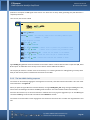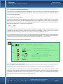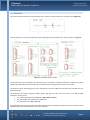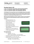
1
C3Synapse SRAM Expansion Board for PropC3 Unit Programming and User Manual Version 1.0 07/12/2012 Author: Francesco de Simone (Digimorf) (Native Italian, forgive my English ) By André LaMothe (Nurve Network LLC) and Francesco de Simone (Digimorf) C3Synapse Manual Version 1.0 By Francesco de Simone SRAM expansion board for PropC3 unit C3Synapse - User Manual v1.0 Copyright © 2012 Nurve Networks LLC, Digimorf Author Francesco de Simone. All rights reserved. No part of this user manual shall be reproduced, stored in a retrieval system, or transmitted by any means, electronic, mechanical, photocopying, recording, or otherwise, without written permission from the publisher. No patent liability is assumed with respect to the user of the information contained herein. Although every precaution has been taken in the preparation of this user manual, the publisher and authors assume no responsibility for errors or omissions. Neither is any liability assumed for damages resulting from the use of the information contained herein. Trademarks All terms mentioned in this user manual those are known to be trademarks or service marks have been appropriately capitalized. Nurve Networks LLC and Digimorf cannot attest to the accuracy of this information. Use of a term in this user manual should not be regarded as affecting the validity of any trademark or service mark. Warning and Disclaimer Every effort has been made to make this user manual as complete and as accurate as possible, but no warranty or fitness is implied. The information provided is on an “as is” basis. The authors and the publisher shall have neither liability nor any responsibility to any person or entity with respect to any loss or damages arising from the information contained in this user manual. The example companies, organizations, products, domain names, e-mail addresses, logos, people, places, and events depicted herein are fictitious. No association with any real company, organization, product, domain name, e-mail address, logo, person, place, or event is intended or should be inferred. eBook License This electronic user manual may be printed for personal use and (1) copy may be made for archival purposes, but may not be distributed by any means whatsoever, sold, resold, in any form, in whole, or in parts. Additionally, the contents of the DVD this electronic user manual came on relating to the design, development, imagery, or any and all related subject matter pertaining to the C3Synapse board are copyrighted as well and may not be distributed in any way whatsoever in whole or in part. Individual programs are copyrighted by their respective owners and may require separate licensing. By André LaMothe (Nurve Network LLC) and Francesco de Simone (Digimorf) Page 1 C3Synapse Manual Version 1.0 By Francesco de Simone SRAM expansion board for PropC3 unit Licensing, Terms & Conditions NURVE NETWORKS LLC, . END-USER LICENSE AGREEMENT FOR C3SYNAPSE HARDWARE, SOFTWARE, EBOOKS, AND USER MANUALS YOU SHOULD CAREFULLY READ THE FOLLOWING TERMS AND CONDITIONS BEFORE USING THIS PRODUCT. IT CONTAINS SOFTWARE, THE USE OF WHICH IS LICENSED BY NURVE NETWORKS LLC, INC., TO ITS CUSTOMERS FOR THEIR USE ONLY AS SET FORTH BELOW. IF YOU DO NOT AGREE TO THE TERMS AND CONDITIONS OF THIS AGREEMENT, DO NOT USE THE SOFTWARE OR HARDWARE. USING ANY PART OF THE SOFTWARE OR HARDWARE INDICATES THAT YOU ACCEPT THESE TERMS. GRANT OF LICENSE: NURVE NETWORKS LLC (the "Licensor") grants to you this personal, limited, non-exclusive, nontransferable, non-assignable license solely to use in a single copy of the Licensed Works on a single computer for use by a single concurrent user only and solely provided that you adhere to all of the terms and conditions of this Agreement. The foregoing is an express limited use license and not an assignment, sale, or other transfer of the Licensed Works or any Intellectual Property Rights of Licensor. ASSENT: By opening the files and or packaging containing this software and or hardware, you agree that this Agreement is a legally binding and valid contract, agree to abide by the intellectual property laws and all of the terms and conditions of this Agreement, and further agree to take all necessary steps to ensure that the terms and conditions of this Agreement are not violated by any person or entity under your control or in your service. OWNERSHIP OF SOFTWARE AND HARDWARE: The Licensor and/or its affiliates or subsidiaries own certain rights that may exist from time to time in this or any other jurisdiction, whether foreign or domestic, under patent law, copyright law, publicity rights law, moral rights law, trade secret law, trademark law, unfair competition law or other similar protections, regardless of whether or not such rights or protections are registered or perfected (the "Intellectual Property Rights"), in the computer software and hardware, together with any related documentation (including design, systems and user) and other materials for use in connection with such computer software and hardware in this package (collectively, the "Licensed Works"). ALL INTELLECTUAL PROPERTY RIGHTS IN AND TO THE LICENSED WORKS ARE AND SHALL REMAIN IN LICENSOR. RESTRICTIONS: (a) You are expressly prohibited from copying, modifying, merging, selling, leasing, redistributing, assigning, or transferring in any matter, Licensed Works or any portion thereof. (b) You may make a single copy of software materials within the package or otherwise related to Licensed Works only as required for backup purposes. (c) You are also expressly prohibited from reverse engineering, decompiling, translating, disassembling, deciphering, decrypting, or otherwise attempting to discover the source code of the Licensed Works as the Licensed Works contain proprietary material of Licensor. You may not otherwise modify, alter, adapt, port, or merge the Licensed Works. (d) You may not remove, alter, deface, overprint or otherwise obscure Licensor patent, trademark, service mark or copyright notices. (e) You agree that the Licensed Works will not be shipped, transferred or exported into any other country, or used in any manner prohibited by any government agency or any export laws, restrictions or regulations. (f) You may not publish or distribute in any form of electronic or printed communication the materials within or otherwise related to Licensed Works, including but not limited to the object code, documentation, help files, examples, and benchmarks. TERM: This Agreement is effective until terminated. You may terminate this Agreement at any time by uninstalling the Licensed Works and destroying all copies of the Licensed Works both HARDWARE and SOFTWARE. Upon any termination, you agree to uninstall the Licensed Works and return or destroy all copies of the Licensed Works, any accompanying documentation, and all other associated materials. By André LaMothe (Nurve Network LLC) and Francesco de Simone (Digimorf) Page 2 C3Synapse Manual Version 1.0 By Francesco de Simone SRAM expansion board for PropC3 unit WARRANTIES AND DISCLAIMER: EXCEPT AS EXPRESSLY PROVIDED OTHERWISE IN A WRITTEN AGREEMENT BETWEEN LICENSOR AND YOU, THE LICENSED WORKS ARE NOW PROVIDED "AS IS" WITHOUT WARRANTY OF ANY KIND, EITHER EXPRESS OR IMPLIED, INCLUDING, BUT NOT LIMITED TO, THE IMPLIED WARRANTIES OF MERCHANTABILITY OR FITNESS FOR A PARTICULAR PURPOSE, OR THE WARRANTY OF NON-INFRINGEMENT. WITHOUT LIMITING THE FOREGOING, LICENSOR MAKES NO WARRANTY THAT (i) THE LICENSED WORKS WILL MEET YOUR REQUIREMENTS, (ii) THE USE OF THE LICENSED WORKS WILL BE UNINTERRUPTED, TIMELY, SECURE, OR ERROR-FREE, (iii) THE RESULTS THAT MAY BE OBTAINED FROM THE USE OF THE LICENSED WORKS WILL BE ACCURATE OR RELIABLE, (iv) THE QUALITY OF THE LICENSED WORKS WILL MEET YOUR EXPECTATIONS, (v) ANY ERRORS IN THE LICENSED WORKS WILL BE CORRECTED, AND/OR (vi) YOU MAY USE, PRACTICE, EXECUTE, OR ACCESS THE LICENSED WORKS WITHOUT VIOLATING THE INTELLECTUAL PROPERTY RIGHTS OF OTHERS. SOME STATES OR JURISDICTIONS DO NOT ALLOW THE EXCLUSION OF IMPLIED WARRANTIES OR LIMITATIONS ON HOW LONG AN IMPLIED WARRANTY MAY LAST, SO THE ABOVE LIMITATIONS MAY NOT APPLY TO YOU. IF CALIFORNIA LAW IS NOT HELD TO APPLY TO THIS AGREEMENT FOR ANY REASON, THEN IN JURISDICTIONS WHERE WARRANTIES, GUARANTEES, REPRESENTATIONS, AND/OR CONDITIONS OF ANY TYPE MAY NOT BE DISCLAIMED, ANY SUCH WARRANTY, GUARANTEE, REPRESENATION AND/OR WARRANTY IS: (1) HEREBY LIMITED TO THE PERIOD OF EITHER (A) Five (5) DAYS FROM THE DATE OF OPENING THE PACKAGE CONTAINING THE LICENSED WORKS OR (B) THE SHORTEST PERIOD ALLOWED BY LAW IN THE APPLICABLE JURISDICTION IF A FIVE (5) DAY LIMITATION WOULD BE UNENFORCEABLE; AND (2) LICENSOR'S SOLE LIABILITY FOR ANY BREACH OF ANY SUCH WARRANTY, GUARANTEE, REPRESENTATION, AND/OR CONDITION SHALL BE TO PROVIDE YOU WITH A NEW COPY OF THE LICENSED WORKS. IN NO EVENT SHALL LICENSOR OR ITS SUPPLIERS BE LIABLE TO YOU OR ANY THIRD PARTY FOR ANY SPECIAL, INCIDENTAL, INDIRECT OR CONSEQUENTIAL DAMAGES OF ANY KIND, OR ANY DAMAGES WHATSOEVER, INCLUDING, WITHOUT LIMITATION, THOSE RESULTING FROM LOSS OF USE, DATA OR PROFITS, WHETHER OR NOT LICENSOR HAD BEEN ADVISED OF THE POSSIBILITY OF SUCH DAMAGES, AND ON ANY THEORY OF LIABILITY, ARISING OUT OF OR IN CONNECTION WITH THE USE OF THE LICENSED WORKS. SOME JURISDICTIONS PROHIBIT THE EXCLUSION OR LIMITATION OF LIABILITY FOR CONSEQUENTIAL OR INCIDENTAL DAMAGES, SO THE ABOVE LIMITATIONS MAY NOT APPLY TO YOU. THESE LIMITATIONS SHALL APPLY NOTWITHSTANDING ANY FAILURE OF ESSENTIAL PURPOSE OF ANY LIMITED REMEDY. SEVERABILITY: In the event any provision of this License Agreement is found to be invalid, illegal or unenforceable, the validity, legality and enforceability of any of the remaining provisions shall not in any way be affected or impaired and a valid, legal and enforceable provision of similar intent and economic impact shall be substituted therefore. ENTIRE AGREEMENT: This License Agreement sets forth the entire understanding and agreement between you and NURVE NETWORKS LLC, supersedes all prior agreements, whether written or oral, with respect to the Software, and may be amended only in a writing signed by both parties. NURVE NETWORKS LLC 12724 Rush Creek Lane Austin, TX 78732 [email protected] www.xgamestation.com Support contacts: [email protected], [email protected] By André LaMothe (Nurve Network LLC) and Francesco de Simone (Digimorf) Page 3 C3Synapse Manual Version 1.0 By Francesco de Simone SRAM expansion board for PropC3 unit A. TABLES OF CONTENT Index B INTRODUCTION ....................................................................................................................................................... 7 C. CONTENT OF THE C3SYNAPSE KIT ............................................................................................................................ 8 Software CD with firmware, drivers and tools ................................................................................................................ 8 The DVD-ROM contains everything you need to learn to use your brand new C3Synapse. ........................................... 8 C3Synapse board ............................................................................................................................................................. 8 D. QUICK START GUIDE ................................................................................................................................................ 9 D.1. Mounting the C3Synapse on the PropC3.............................................................................................................. 11 D.2. The first test of the C3Synapse: setup phase ....................................................................................................... 13 D.3. The first test of the C3Synapse: execution phase................................................................................................. 14 E. INSIDE THE C3SYNAPSE .......................................................................................................................................... 21 E.1. The interface of the C3Synapse ............................................................................................................................ 21 E.2. The command decoder ......................................................................................................................................... 22 E.3. The core of the C3Synapse: the 512Kbytes SRAM chip ........................................................................................ 25 E.4. The memory addressing system ........................................................................................................................... 26 E.4.1.The address low nibble latch ................................................................................................................................ 27 E.4.2.The low nibble clocking sequence ........................................................................................................................ 29 E.4.3.The middle and high nibble latch ......................................................................................................................... 31 E.4.4.The memory reading and writing procedure ....................................................................................................... 33 F. PROGRAMMING THE C3SYNAPSE .......................................................................................................................... 36 F.1. Initializing the C3Synapse ..................................................................................................................................... 36 F.2. The status LED routine .......................................................................................................................................... 37 F.3. Set the memory address routine .......................................................................................................................... 38 F.4. Write byte routine ................................................................................................................................................ 39 F.5. Read byte routine ................................................................................................................................................. 40 F.6. Write block of bytes routine ................................................................................................................................. 41 F.7. Read block of bytes routine .................................................................................................................................. 42 F.8. C3Synapse advanced programming ..................................................................................................................... 43 F.9. C3Synapse and PropellerGCC ............................................................................................................................... 43 G. C3SYNAPSE DEMOS ............................................................................................................................................... 44 G.1. VGM player demo ................................................................................................................................................. 45 By André LaMothe (Nurve Network LLC) and Francesco de Simone (Digimorf) Page 4 C3Synapse Manual Version 1.0 By Francesco de Simone SRAM expansion board for PropC3 unit G.2. Photo frame demo ............................................................................................................................................... 46 G.3. Font demo ............................................................................................................................................................ 48 G.4. TV driver demo ..................................................................................................................................................... 49 H. EXPANDING THE C3SYNAPSE ................................................................................................................................. 50 H.1. Expansion examples ............................................................................................................................................. 51 H.2. C3Synapse and other microcontroller boards ...................................................................................................... 52 I. C3SYNAPSE DRIVERS .............................................................................................................................................. 53 J. APPENDICES AND BONUS MATERIAL ..................................................................................................................... 54 J.1. How to create the micro SD card for test and demos .......................................................................................... 54 J.1. Support stuff ......................................................................................................................................................... 55 J.2. C3Synapse TV driver color chart ........................................................................................................................... 56 J.1. Conversion table ................................................................................................................................................... 57 J.1. Schematics ............................................................................................................................................................ 63 J.2. LED Tester ............................................................................................................................................................. 68 Table of figures Figure 1: DVD-ROM. ................................................................................................................................................................. 8 Figure 2: C3Synapse Board. ...................................................................................................................................................... 8 Figure 3: The C3Synapse Board. ............................................................................................................................................... 9 Figure 4: C3Synapse board. .................................................................................................................................................... 10 Figure 5: Annotated PropC3. .................................................................................................................................................. 11 Figure 6: Bottom side of C3Synapse. ..................................................................................................................................... 12 Figure 7: Views of the C3Synapse stacked on top of the PropC3 . ........................................................................................ 12 Figure 8: Parallax Serial Terminal program. ........................................................................................................................... 14 Figure 9: Power LED when PropC3 powers up. ...................................................................................................................... 14 Figure 10: C3Synapse test program main menu. ................................................................................................................... 15 Figure 11: Virtual keyboard function. .................................................................................................................................... 15 Figure 12: First memory write/read test. ............................................................................................................................... 16 Figure 13: Third Memory write/read test. ............................................................................................................................. 16 Figure 14: The system header of the C3Synapseboard. ......................................................................................................... 17 Figure 15: The OUT lines test. ................................................................................................................................................ 17 Figure 16: The Status LED on the C3Synapse board............................................................................................................... 18 Figure 17: The Status LED test screen. ................................................................................................................................... 18 Figure 18: The test pattern picture showed on the screen. ................................................................................................... 19 Figure 19: Insert SD Card message. ........................................................................................................................................ 19 Figure 20: The C3Synapse headers. ....................................................................................................................................... 21 Figure 21: The C3Synapse/PropC3 header. ............................................................................................................................ 21 Figure 22: C3Synapse command decoder stage. ................................................................................................................... 22 Figure 23: Decoder stage. ...................................................................................................................................................... 23 By André LaMothe (Nurve Network LLC) and Francesco de Simone (Digimorf) Page 5 C3Synapse Manual Version 1.0 By Francesco de Simone SRAM expansion board for PropC3 unit Figure 24: Status LED circuit. .................................................................................................................................................. 24 Figure 25: SRAM IC. ................................................................................................................................................................ 25 Figure 26: “6T” SRAM Cell (6 Transistors). ............................................................................................................................. 25 Figure 27: IS61LV5128AL pins configuration. ......................................................................................................................... 26 Figure 28: Low nibble addressing circuit (latch)..................................................................................................................... 27 Figure 29: Low nibble addressing circuit. ............................................................................................................................... 28 Figure 30: Low nibble addressing circuit (sequential action). ................................................................................................ 30 Figure 31: Middle and high nibble addressing circuit (latch). ................................................................................................ 31 Figure 32: Middle and high nibble addressing circuit. ........................................................................................................... 32 Figure 33: SRAM circuit. ......................................................................................................................................................... 34 Figure 35: VGM music player demo music loader. ................................................................................................................ 45 Figure 36: VGM music player demo playing screen. .............................................................................................................. 45 Figure 37: VGM music player demo start screen. .................................................................................................................. 45 Figure 39: Photo frame demo, art picture. ............................................................................................................................ 46 Figure 40: Photo frame demo, Iron man 2 picture. ............................................................................................................... 46 Figure 41: Photo frame demo, Transformers 2 picture. ........................................................................................................ 46 Figure 42: Photo frame demo, Wolverine picture. ................................................................................................................ 47 Figure 43: Photo frame demo, tropical picture...................................................................................................................... 47 Figure 44: Photo frame demo, Airwolf picture. ..................................................................................................................... 47 Figure 45: Photo frame demo, Megan Fox picture. ............................................................................................................... 47 Figure 47: Font demo, example. ............................................................................................................................................ 48 Figure 50: Middle and high nibble addressing circuit (latch). ................................................................................................ 50 Figure 52: Arduino IDE with a blink program. ........................................................................................................................ 52 Figure 53: PropC3 Micro SD card slot. ................................................................................................................................... 54 Figure 54: 2GB Micro SD card (SanDisk, Kingston, etc. 1GB-2GB is fine). .............................................................................. 54 Figure 55: C3Synapse TV driver color palette. ....................................................................................................................... 56 Figure 56: Power LED circuit. ................................................................................................................................................. 63 Figure 57: C3Synapse headers circuits. .................................................................................................................................. 63 Figure 58: Command decoder IC1 SN74ACT138D circuit. ...................................................................................................... 64 Figure 59: STATUS LED Circuit. ............................................................................................................................................... 64 Figure 60: Low nibble address circuit. .................................................................................................................................... 65 Figure 61: Middle and high nibble latching system. .............................................................................................................. 66 Figure 62: SRAM interface circuit........................................................................................................................................... 66 Figure 63: LED tester on a little breadboard. ......................................................................................................................... 68 Figure 64: LED tester connected to the C3Synapse. .............................................................................................................. 68 Figure 65: LED tester connected to the C3Synapse. .............................................................................................................. 69 Figure 66: Custom LED Tester for the C3Synapse. ................................................................................................................. 69 By André LaMothe (Nurve Network LLC) and Francesco de Simone (Digimorf) Page 6 C3Synapse Manual Version 1.0 By Francesco de Simone SRAM expansion board for PropC3 unit B. INTRODUCTION Welcome to “C3Synapse Expansion Board”. C3Synapse is an expansion board designed for PARALLAX PropC3 Unit. It adds extra 512Kb of fast static RAM to PropC3 and gives to PropC3 the control of 5 extra output lines. This hands-on guide covers the design and hardware of the C3Synapse as well as demos and tutorials to get you going fast. First and foremost the C3Synapse is an expansion board designed for PropC3 unit. PropC3 is a Propeller-based product, so everything you know about the PropC3 and multicore Propeller microcontroller applies. If you’re a seasoned expert then you might just want to skim this manual focusing on the schematic and the main routines to access the board since that’s all you need to get started. This manual does not teach you Spin, assembly language, graphics, or how to write drivers for the Propeller chip. This manual only covers the C3Synapse hardware and software demos that come with it. If there is particular material that is beyond the scope of this manual, I will refer you to one of the books above in many cases. Of course, I hope you by default read the Propeller Reference Manual itself! Otherwise you should start here at the Parallax Propeller site to see what’s available online: www.parallax.com/propeller Specifically be sure to review these documents especially: Propeller Manual (from the Propeller Downloads link). Propeller Datasheet (from the Propeller Downloads link). Propeller Questions & Answers system (from the Propeller Q&A link). Also, there are a number of printed books about the Propeller you might want to pick up and read: Programming and Customizing the Multicore Propeller Microcontroller, Parallax. Game Programming for the Propeller Powered HYDRA, André LaMothe. Programming the Propeller with Spin, A Beginners Guide to Parallel Processing, Harprit Sandhu. When you have familiarized with the Propeller microcontroller, you should read carefully the manual “Unleashing the TM Propeller C3” by André LaMothe: http://www.parallax.com/Portals/0/Downloads/docs/prod/prop/UnleashingPropellerC3v1.0.pdf Which will guide you in mastering PropC3, and then you will want to read this manual carefully. Now you are ready to see what’s included in the kit! By André LaMothe (Nurve Network LLC) and Francesco de Simone (Digimorf) Page 7 C3Synapse Manual Version 1.0 By Francesco de Simone SRAM expansion board for PropC3 unit C. CONTENT OF THE C3SYNAPSE KIT Software CD with firmware, drivers and tools The DVD-ROM contains everything you need to learn to use your brand new C3Synapse. DVD-ROM Contents: Figure 1: DVD-ROM. FTDI USB Windows drivers. PARALLAX Propeller IDE v1.3. Test Firmware for PropC3 unit. Files needed by the firmware during tests. SPIN/Assembly Drivers. Demos. Manuals. Schematics. Goodies. C3Synapse board This is the memory expansion board to be stacked on your PropC3, see the Figure 2 below. Figure 2: C3Synapse Board. By André LaMothe (Nurve Network LLC) and Francesco de Simone (Digimorf) Page 8 C3Synapse Manual Version 1.0 By Francesco de Simone SRAM expansion board for PropC3 unit D. QUICK-START GUIDE In this brief quick-start guide we are going to review the C3Synapse briefly, mount it on a PropC3, power it up, and run the test demo. This will confirm everything is working properly as well as familiarize you with the C3Synapse board itself. First off, take a look at Figure 3 which is your C3Synapse board. Figure 3: The C3Synapse Board. Take a detailed look at the C3Synapse by looking at Figure 4, which is an annotated image of the board. Review all the interfaces and location of various components. Later we will drill down closer and each of the I/O headers and chips used by the C3Synapse will be illustrated, but for now, just get a birds-eye view of the board. By André LaMothe (Nurve Network LLC) and Francesco de Simone (Digimorf) Page 9 C3Synapse Manual Version 1.0 By Francesco de Simone SRAM expansion board for PropC3 unit (1) Power LED . (3) Expansion header . (4) Interface header . (2) Status LED . (6) Tri-Ports headers . (5) Analogue header . Figure 4: C3Synapse board. (1) Power LED. It shows you when the board receives power from the PropC3. (2) Status LED. It turns on when you activate its line. You can use it for debugging purposes. (3) Expansion header. Here there are 5 out lines, 3 system lines (Read, Write and Clock) and power lines (3.3v, 5v and GND) that you can use to expand your C3Synapse. (4) Interface header. Here all the PropC3 bus lines are available for future use. Refer to PropC3 docs. (5) Analogue header. C3Synapse doesn’t use these lines. They are only carried on top of the C3Synapse for an easy use. (6) Tri-Ports header. C3Synapse doesn’t use these lines. They are only carried on top of the C3Synapse for an easy use. C3Synapse has been designed with stackable pass-through headers to let you take advantage of the other resources of the PropC3. As you will learn later in this manual, you will be able to take the best from both boards for other projects. Now, take a look at Figure 5 below, which is an annotated image of the PropC3 board. Take a moment to review all the interfaces and connectors. You probably already know the PropC3, but you should notice that the C3Synapse board has the same form factor and position of headers of the PropC3 and can be stacked perfectly on top. By André LaMothe (Nurve Network LLC) and Francesco de Simone (Digimorf) Page 10 C3Synapse Manual Version 1.0 By Francesco de Simone SRAM expansion board for PropC3 unit Figure 5: Annotated PropC3. Now that you have an idea of what goes where, let’s move on and follow the next section to setup the C3Synapse and the PropC3 for the first time. D.1. Mounting the C3Synapse on the PropC3 The following steps will guide you in mounting the C3Synapse on top of the PropC3 in order to work with it. Follow them carefully. STEP 1: Make sure you follow these simple anti-static precautions before handling the C3Synapse board: Touch a metal window-frame or similar with your finger before handling the PCB. Only handle the edges of the PCB and avoid touching microchips with your fingers. STEP 2: Prepare your PropC3 on the table and take your C3Synapse out from the plastic anti-static envelope. You should see the interface pins on the bottom side of the board. These pins have their corresponding headers on the PropC3 (Figure 6). By André LaMothe (Nurve Network LLC) and Francesco de Simone (Digimorf) Page 11 C3Synapse Manual Version 1.0 By Francesco de Simone SRAM expansion board for PropC3 unit Figure 6: Bottom side of C3Synapse. STEP 3: Once you have understood the correct orientation, carefully position the C3Synapse on top of the PropC3. As you perform this operation be sure that all corresponding headers and pins are aligned, then gently insert the board until the pins are all seated, if the pins don’t insert easily try “rocking” the board a little to get the pins to slide in. Take a moment to inspect all sides of the board to assure that all pins are perfectly inserted on their header. See Figure 7 below. Figure 7: Views of the C3Synapse stacked on top of the PropC3. There you go! Nothing difficult really, but every time you mount/unmount the C3Synapse on/from the PropC3 you should take care, so that you won’t damage pins or the boards. The C3Synpase board mounts on top of the PropC3, however, due to the tight clearance, make sure to inspect the area above the PS/2 connector. Its metal housing may come in contact with the underside of the C3Synapse PCB. A simple safeguard it to place a piece of electrical tape under the C3Synpase or on top of the PS/2's metal connector, as show in Figure 7(a-c). Figure 7(a-c): Details of the PS2 connector and the piece of electric tape. By André LaMothe (Nurve Network LLC) and Francesco de Simone (Digimorf) Page 12 C3Synapse Manual Version 1.0 By Francesco de Simone SRAM expansion board for PropC3 unit D.2. The first test of the C3Synapse: setup phase You are going to have your first test with the C3Synapse. To accomplish this task you need a TV video monitor that can catch the NTSC signal and of course the PC you use to program the PropC3. Let’s see how to do it quickly. Plug the video composite cable to “Video out” port of PropC3 to your NTSC monitor/TV “Video in” port. Confirm that the power switch of the PropC3 is in the OFF position (to the right). Now you can plug the USB mini cable to PropC3 USB port and to a free PC USB port. I assume that if you have a PropC3 you should have already used the Propeller Tool also. Otherwise, take some time to get familiar with it by reading some books/docs on Propeller. When you are familiar with uploading a binary file or a SPIN program on PropC3, you can move on. It’s time now to burn the test firmware on PropC3 unit. Open the Propeller Tool and navigate to the main menu [“File”] [Open...]. Or simply press [CTRL+O] keys. Next, locate the firmware file on DVD-ROM. C3Synapse Test Suite Firmware [C3SYNAPSE DVD-ROM Root] C3Synapse/Tools/PropC3 _Firmware.eeprom After the load option is confirmed, the “Object Info” window appears. You can ignore all technical information about this file and simply click on the [load EEPROM] button. The firmware will start burning into the PropC3 unit - easy! Before starting the full test session, you need to activate the Serial Terminal program from the Propeller Tool. It allows you to control the PropC3 via the PC keyboard over the USB serial connection. In this way you won’t need an extra PS2 keyboard connected to the PropC3! To open the Serial Terminal program select the menu [“Run”] [Parallax Serial Terminal...] from Propeller Tool, or simply press [F12] key on the PC keyboard. This opens the PARALLAX “Serial Terminal program” window. The PropC3 firmware handles serial communications at 115,200 Baud, so verify this value is set correctly, and otherwise change it. Also verify that the COM port number is the same you are using to program your PropC3. Basically the Parallax Serial Terminal window should look similar to Figure 8 shown below. Verify that you have the same settings you see here for Baud Rate, check boxes, and echo on (your COM port will be different of course). By André LaMothe (Nurve Network LLC) and Francesco de Simone (Digimorf) Page 13 C3Synapse Manual Version 1.0 By Francesco de Simone SRAM expansion board for PropC3 unit Figure 8: Parallax Serial Terminal program. If you focus on another window, or switch to another application running on Windows, the terminal will be “disabled” and put in stand-by mode. To re-enable it, just go back to the terminal application (usually ALT+TAB keys) and click on [Enable] button. Now you can click inside the “yellow” input area on top of the window to enable keyboard input. Perfect, you are ready! D.3. The first test of the C3Synapse: execution phase In this section you will perform the Full Test to check if C3Synapse is working properly. This will give you a first overview of the features of C3Synapse. Turn on your TV monitor and select the correct video source that came from the PropC3. Turn on the unit also and you will see the power green LED of the C3Synapse board turning on. See Figure 9 below. Figure 9: Power LED when PropC3 powers up. As soon as the program on the PropC3 starts, the main menu should appear on your TV monitor screen (Figure 10): By André LaMothe (Nurve Network LLC) and Francesco de Simone (Digimorf) Page 14 C3Synapse Manual Version 1.0 By Francesco de Simone SRAM expansion board for PropC3 unit Figure 10: C3Synapse test program main menu. Option [1] performs a full test, while options from [2] to [10] perform single tests and should be used when you want to test each single feature. To start the full test you need to activate the Serial Terminal program and type “1” in the yellow input area and “a-ha”, on the TV monitor you should see “1” near the text “Selection >” (Figure 11)! Figure 11: Virtual keyboard function. Now press the “ENTER” key on terminal to confirm the option, exactly as if you had a keyboard plugged to the PropC3 unit. The full test starts and automatically performs all checks to verify that the C3Synapse board works properly. It starts with three memory writing/reading cycles. The first cycle writes the byte “0x00” along the entire memory space. For each write, it reads the byte back to check if the written value is the same (Figure 12). By André LaMothe (Nurve Network LLC) and Francesco de Simone (Digimorf) Page 15 C3Synapse Manual Version 1.0 By Francesco de Simone SRAM expansion board for PropC3 unit Figure 12: First memory write/read test. The second cycle tries to write a byte “0xAA” along the entire memory space while the third one tries to write the byte “0xFF”. If something goes wrong in any of these tests, you will see an error message that tells you the read byte is not the byte just written. Figure 13 illustrates an example of a possible error. Figure 13: Third Memory write/read test. If something doesn’t work correctly inside the C3Synapse’s memory access test it means that the byte read doesn’t correspond to the byte written, so press “ESC” key and repeat the test. If you see the error message again, then turn off the PropC3 and inspect the assembly to see if every pin is inserted in its header hole properly. If everything is ok, then maybe the board may be damaged in some way. Follow the warranty section for any problems. By André LaMothe (Nurve Network LLC) and Francesco de Simone (Digimorf) Page 16 C3Synapse Manual Version 1.0 By Francesco de Simone SRAM expansion board for PropC3 unit The full test program now continues by testing the output lines, which are located on the system header of the C3Synapse board (Figure 14). Figure 14: The system header of the C3Synapseboard. There’s no way for the software to get any feedback if these lines work properly (Figure 15). Actually, they have been already tested during manufacturing process, so if you want to visually verify them, you can plug some LEDs or use a special LED tester (shown in section J.2 LED tester). If you are going to develop software that uses the C3Synapse you might want to have a visual feedback of what you are doing. Figure 15: The OUT lines test. There are 5 OUT lines that are checked following a binary counter-up sequence. If you had LEDs connected to these lines, you would see this sequence: 00000 00001 00010 00011 00100 00101 00110 00111 … 11111 After this test, the program will drive the system lines following this sequence: Write Read Clock. By André LaMothe (Nurve Network LLC) and Francesco de Simone (Digimorf) Page 17 C3Synapse Manual Version 1.0 By Francesco de Simone SRAM expansion board for PropC3 unit The last test is the Status LED test. This LED is located on the right side of the C3Synapse near the middle of the board/right header. Figure 16 shows where this LED is. Figure 16: The Status LED on the C3Synapse board. In this test this LED will rapidly blink 10 times. The screen will show you only that the test is performed (Figure 17). You must check if the LED lights up. No problem if you can’t count how many times it lights up, the important is that it does! Figure 17: The Status LED test screen. At the end of the initial memory tests, an image from the SD card is loaded into the C3Synapse memory and displayed on the NTSC monitor; this will give you a “visual” test to verify if the memory is working properly. If the memory isn’t working, you will “see” problems visually very quickly. Make sure you have a test SD card inserted into the SD card slot of the PropC3. You should see the “Test” image on TV monitor as shown below (Figure 18). By André LaMothe (Nurve Network LLC) and Francesco de Simone (Digimorf) Page 18 C3Synapse Manual Version 1.0 By Francesco de Simone SRAM expansion board for PropC3 unit Figure 18: The test pattern picture showed on the screen. Note: if you haven’t inserted a SD card in the PropC3 SD card slot, the program will prompt you to insert one to continue with the test (Figure 19). Figure 19: Insert SD Card message. This phase of the test is important as well as the previous tests. If the program can’t find a test SD card in the slot, it will retry to read the slot until you insert an SD card. Additionally, try ejecting and reinserting the SD card if there are read problems. By André LaMothe (Nurve Network LLC) and Francesco de Simone (Digimorf) Page 19 C3Synapse Manual Version 1.0 By Francesco de Simone SRAM expansion board for PropC3 unit To build the test SD card, refer to “Section J.1 How to create the micro SD card for test and demos”. The bitmap image showed on the screen is useful to quickly check if the overall function of the C3Synapse is correct. In fact, pixel data are stored in the C3Synapse’s SRAM frame buffer and then read in real time and sent to the TV monitor. This final test uses all features of the C3Synapse as fast as possible to really test it and make sure its 100%! While the C3Synapse shows the image on the screen, the system control lines (Write, Read and Clock) are continuously accessed, so if you had some LEDs connected to these lines you should see them still. The test is now complete and we can go deeper in C3Synapse functions. In the next section you will learn how it works. By André LaMothe (Nurve Network LLC) and Francesco de Simone (Digimorf) Page 20 C3Synapse Manual Version 1.0 By Francesco de Simone SRAM expansion board for PropC3 unit E. INSIDE THE C3SYNAPSE This section shows you how actually the C3Synapse works. You will learn the functions of each IC and how it interfaces to the PropC3. At the end you will be ready to develop some programs that use your C3Synapse! E.1. The interface of the C3Synapse The C3Synapse board interfaces to the PropC3 with some lines of the bus. Have a look at Figure 20. (1) (3) (2) Figure 20: The C3Synapse headers. Headers (2) and (3) are not used by the C3Synapse. They are only carried on top for an easy use of them. C3Synapse shares the same signals of the PropC3 Bus through Header (1) instead. In particular it uses lines from [P7:P0] as an 8-bit data bus, while lines from [P18:P16] are used to select all functions of the C3Synapse. Figure 21 highlights these shared lines. Figure 21: The C3Synapse/PropC3 header. If you are familiar with SPIN the following code can be used to access to the data lines, and keep in mind that data bus is bi-directional. By André LaMothe (Nurve Network LLC) and Francesco de Simone (Digimorf) Page 21 C3Synapse Manual Version 1.0 By Francesco de Simone SRAM expansion board for PropC3 unit DIRA [7..0] := %11111111 OUTA [7..0] := Byte to send DIRA [7..0] := %00000000 Byte to read := INA [7..0] You should do in the same way for control lines also, but only in output direction. DIRA [18..16] := %111 OUTA [18..16] := bits to send In this case you will have 3 bits only for the range of values between 0 and 7. Thus you will have 8 commands that can be sent to the C3Synapse, cool! We will come back to this later on in the manual, in the programming section. E.2. The command decoder In order to control all functions of the C3Synapse you have to access to the command decoder with control lines associated to the pins [P18:P16]. Look at the schematic in Figure 22, the circuit is very simple. Figure 22: C3Synapse command decoder stage. Decoding the 3 address lines is accomplished by the 3 8 bit decoder (IC1 – 74*138 family chips). According to the binary value read on “CTRL_#” lines, IC1 will enable one of the n outputs (active LOW). These outputs are directly connected to the active LOW chip select line of each IC that drives the Static RAM IC. By André LaMothe (Nurve Network LLC) and Francesco de Simone (Digimorf) Page 22 C3Synapse Manual Version 1.0 By Francesco de Simone SRAM expansion board for PropC3 unit 74 * 138 family datasheet [C3SYNAPSE DVD-ROM Root] C3Synapse\Hardware\Components_Datasheets\Integrated_Circuits\74LV138.pdf As you can see from the picture below (Figure 23), you can find the IC1 on PCB near the bus. Figure 23: Decoder stage. The Propeller feeds the 3 bits labeled [CTRL_2:CTRL_0] into the decoder IC1 at inputs A, B, C on pins 1, 2, 3 respectively. Thus, the binary value sent selects lines [Y7:Y0] to assert (active LOW) on the decoder. These signals are referred in the schematic with the name of their function discussed later on in this manual. Therefore, to select any of these lines the SPIN algorithm is very simple, you need to send the command using the value of Yn, and then 0 (which corresponds to Y0 non connected) to reset the decoder. { Let's say we want to enable the CMD_WR to send a Byte, we need to activate the line Y1. Thus we need to send value "1" } OUTA [18..16] := %001 { It's a good habit to reset the decoder after any command has been sent. If you send the value "0" the line Y0 will be selected, but since it's not connected to anything every other lines Y will be reset. } OUTA [18..16] := %000 As you should have noticed, the line Y7 of the decoder is connected to the Status LED circuit (Figure 24). When the line is asserted (active LOW) it makes the LED turn on. By André LaMothe (Nurve Network LLC) and Francesco de Simone (Digimorf) Page 23 C3Synapse Manual Version 1.0 By Francesco de Simone SRAM expansion board for PropC3 unit Figure 24: Status LED circuit. You already saw this LED at work during the full test, now you know how to drive it, and use it as a debug tool. Let’s see how: DIRA [18..16] := %111 repeat 10 { We will active the line Y7 by sending the value "7" to the decoder, then we will wait for a second ( assuming the main clock is set to 80Mhz ) } OUTA [18..16] := %111 waitcnt( cnt + 80_000_000 ) { Then we will active the line Y0 by sending the value "0" to the decoder, this will turn off the LED. Then we will wait for another second } OUTA [18..16] := %000 waitcnt( cnt + 80_000_000 ) { If you send this in a loop you will see Status LED blinking with a pause of 1 second each. } Now if you put this example in a SPIN template you should have a program like the following one: CON _CLKmode = xtal1 + pll16x _xinfreq = 5_000_000 PUB main DIRA [18..16] := %111 repeat 10 { We will active the line Y7 by sending the value "7" to the decoder, then we will wait for a second ( assuming the main clock is set to 80Mhz ) } OUTA [18..16] := %111 waitcnt( cnt + 80_000_000 ) { Then we will active the line Y0 by sending the value "0" to the decoder, this will turn off the LED. Then we will wait for another second } OUTA [18..16] := %000 waitcnt( cnt + 80_000_000 ) { If you send this in a loop you will see Status LED blinking with a pause of 1 second each. } By André LaMothe (Nurve Network LLC) and Francesco de Simone (Digimorf) Page 24 C3Synapse Manual Version 1.0 By Francesco de Simone SRAM expansion board for PropC3 unit This is pretty cool, right? At this point you know how to send a command to the C3Synapse. Now you can try making changes to this program to see how fast the LED can blink, or try setting different delay values for “OFF” and “ON” status of the LED. E.3. The core of the C3Synapse: the 512Kbytes SRAM chip The core of this board is a parallel Static RAM chip that can store up to 512Kbytes of data. You can see it in Figure 25. Figure 25: SRAM IC. Since the C3Synapse is designed around this IC, it’s important that we really understand how it works at a high level as well as a low level, so let's take a look at a single SRAM memory cell. Static Random Access Memory (SRAM) is a type of semiconductor memory that uses bistable latching circuitry to store each bit. The Figure 26 below shows a typical static cell circuit that stores one bit. Figure 26: “6T” SRAM Cell (6 Transistors). Each bit in an SRAM cell is stored using four transistors (M1, M2, M3 and M4) that form two cross-coupled inverters. This storage cell has two stable states which are used to denote “0” and “1”. Two additional access transistors serve to control the access to a storage cell during read and write operations. A typical SRAM uses six MOSFETs (Metal Oxide Semiconductor Field Effect Transistor) to store each memory bit. The C3Synapse uses 10 Transistors cells technology (10T) instead. By André LaMothe (Nurve Network LLC) and Francesco de Simone (Digimorf) Page 25 C3Synapse Manual Version 1.0 By Francesco de Simone SRAM expansion board for PropC3 unit Semiconductor theory is quite complex! There are numerous types of “transistors”, but they fall into two major categories: Junction transistors and field effect transistors. Junction transistors are constructed by creating N and P type materials and then literally placing them in contact with each other to create the transistor action. Field effect transistors operate on a different premise where an electric field causes a “channel” of positive or negative charge to accumulate which is then used as the transistor action. Most modern chips use the later type of transistor due to its lower power and cost. The term static differentiates it from Dynamic RAM (DRAM) which must be periodically refreshed. This makes them faster and lets them reach higher speed. C3Synapse mounts an IS61LV5128AL-10TLI (IC7). This IC has 512 K * 8 memory cells (512 Kb) and has an access time of 10ns, which lets you reach the maximum speed of 100Mhz. More than enough required for a Propeller based system. IS61LV5128AL-10TLI Datasheet [C3SYNAPSE DVD-ROM Root] C3Synapse\Hardware\Components_Datasheets\Integrated_Circuits\IS61LV5128AL-10TLI.pdf As all SRAMs do, also this chip exhibits data permanence, but it is still volatile in the conventional sense that data is eventually lost when the memory is not powered. If you store data, it will still remain unless you disconnect the USB cable from the PropC3. Data still remain there even if you turn off power switch on the PropC3. This is useful for debugging purposes, because when you store data with one SPIN program, then you can upload another program that let you check memory locations and see if values were correctly stored. Not bad! E.4. The memory addressing system At this point, we can see how this memory works inside the C3Synapse. First of all have a look at the pin configuration of IS61LV5128AL-10TLI in Figure 27. Pins [A7:A0] are active high address lines, pins from [I/O7:I/O0] are active high data lines while the chip control lines are CE, OE and WE active low. It’s very simple to use this memory! Figure 27: IS61LV5128AL pins configuration. By André LaMothe (Nurve Network LLC) and Francesco de Simone (Digimorf) Page 26 C3Synapse Manual Version 1.0 By Francesco de Simone SRAM expansion board for PropC3 unit Address lines have been divided in 3 groups so that it is possible to control them with only 8 lines (3 * 8 = 24). Thus we have 3 nibbles to set for a complete address setup procedure. LOW Nibble: MIDDLE Nibble: HIGH Nibble: [A7:A0] [A15:A8] [A18:A16] (8-bits) (8-bits) (3-bits) We can setup the address in three times by sending 3 values to the C3Synapse through the data bus. To build the whole address there is a different latch system for each nibble, which must be activated to store each value. The algorithm to setup the memory address is: Step 1, Send low nibble value, latch low nibble Step 2, Send middle nibble value, latch middle nibble Step 3, Send high nibble value, latch high nibble After this procedure the whole address is setup and a memory location can be accessed for reading or writing. That said, let’s see how each latch system works. E.4.1. The address low nibble latch Low nibble [A7:A0] is handled by two 4-bits latch/counters (IC2, IC3) that not only store a value, but even has an internal counter. This lets you setup the value and then you simply have to feed the counter with a clock pulse to advance in the address space. Let’s have a look at the schematic in the Figure 28 below. Figure 28: Low nibble addressing circuit (latch). By André LaMothe (Nurve Network LLC) and Francesco de Simone (Digimorf) Page 27 C3Synapse Manual Version 1.0 By Francesco de Simone SRAM expansion board for PropC3 unit The 74HC161D is a latch/counter IC that can store a 4-bit value in parallel using the Latch signal, and then count sequentially using the Count signal. 74HC161D Datasheet [C3SYNAPSE DVD-ROM Root] C3Synapse\Hardware\Components_Datasheets\Integrated_Circuits\74HC161D.pdf These two ICs are located on the left of the SRAM IC, see Figure 29 below. Figure 29: Low nibble addressing circuit. It’s time now to see how this stage works. To latch a value into the counter we first need to provide a 4-bit value on the data lines A, B, C, and D. When these signals "settle" the signal LD (LOAD, active LOW) must be asserted to store the value in the internal buffer of the counter IC. When dealing with integrated circuits, they operate very fast, but not infnitely fast, thus it takes a finite amount of time, usually measure in nanoseconds before signals stablize and or propagate in the chip. These values are listed in the chip's data sheet, under names such as "holding time" or "settling time". In this case the two ICs share the same LD line, in this way the value in data lines is stored in two halves at the same time. This signal is labeled SRAM_A0-7_CS and connects both LD signals of IC2 and IC3 to the command decoder IC1 port Y6. These ICs need also to be clocked once to buffer the value, that’s why the LD signal goes through some NAND gates that delay it, and then it arrives to the NAND gate connected to the CLK signal (which is always HIGH in this kind of access) and By André LaMothe (Nurve Network LLC) and Francesco de Simone (Digimorf) Page 28 C3Synapse Manual Version 1.0 By Francesco de Simone SRAM expansion board for PropC3 unit produces a clock pulse on CLK signal of IC2 and IC3. You don’t have to worry about generating this pulse because it’s completely automatic. Let’s see now, how to do it in SPIN. CON _CLKmode = xtal1 + pll16x _xinfreq = 5_000_000 PUB main | Address Address := $12ACF ' An arbitrary value within the memory address space ' $00000 .. $7FFFF ' Setup direction of lines DIRA [18..16] := %111 DIRA [7..0] := %11111111 OUTA [7..0] := %00000000 ' Resets lines to prevent any accidental value OUTA [18..16] := %000 ' Resets lines to prevent any accidental value OUTA [7..0] := Address & $FF ' Sends the low nibble of the address OUTA [18..16] := %110 ' Sends the value "6",Y6 of command decoder OUTA [18..16] := %000 ' Resets and finalizes the command on latch Signal SRAM_A0-7_CS needs to be asserted then de-asserted to make IC1 and IC2 latch the value in input lines A, B, C and D like a pulse. As said before this is the way to set a value for the first nibble of the address. This step may be used for a random access to the memory or as a starting location for reading/writing a memory block. Now you will see how perform a clocked auto-increment on low nibble. E.4.2. The low nibble clocking sequence IC2 and IC3 can be clocked by trigging the clock signal to increment by 1 the value stored in their buffer. Let’s have a look at the schematic in the Figure 30. When you pulse the signal Y3 of the command decoder, the signal SRAM_A0-7_CNT will go through a NAND gate of IC4, which returns an HIGH signal and drives the CLK signal of IC2 and IC3. The value in buffer will be incremented by 1. Once this value reaches 15, on the next increment it overflows and a carry signal is triggered on pin 15. This RCO signal connected to ENT signal can be used to activate another 74HC161 in cascade. IC2 and IC3 are used to buffer a value ranging from 0 to 255 and to count from n0 to n1 within the range between 0 and 255. By André LaMothe (Nurve Network LLC) and Francesco de Simone (Digimorf) Page 29 C3Synapse Manual Version 1.0 By Francesco de Simone SRAM expansion board for PropC3 unit Figure 30: Low nibble addressing circuit (sequential action). Let’s see how to do this in SPIN: CON _CLKmode = xtal1 + pll16x _xinfreq = 5_000_000 PUB main | Address Address := $12ACF ' An arbitrary value within the memory address space ' $00000 .. $7FFFF ' Setup direction of lines DIRA [18..16] := %111 DIRA [7..0] := %11111111 OUTA [7..0] := %00000000 ' Resets lines to prevent any accidental value OUTA [18..16] := %000 ' Resets lines to prevent any accidental value OUTA [7..0] := Address & $FF ' Sends the low nibble of the address OUTA [18..16] := %110 ' Sends the value "6",Y6 of command decoder OUTA [18..16] := %000 ' Resets and finalizes the command on latch By André LaMothe (Nurve Network LLC) and Francesco de Simone (Digimorf) Page 30 C3Synapse Manual Version 1.0 By Francesco de Simone SRAM expansion board for PropC3 unit ' This first step has setup the Low nibble to $CF, now we can start from this value to increment the location of memory. repeat 16 OUTA [18..16] := %011 ' Sends the value "6",Y6 of command decoder OUTA [18..16] := %000 ' Resets and finalizes the command on latch Very Simple! Later on in the manual you will learn how to write/read a value on SRAM. E.4.3. The middle and high nibble latch Middle and High nibbles are handled by two 8-bits that store a value by asserting the CLK signal of the chip. Let’s have a look at the schematic in the Figure 31 shown below. Figure 31: Middle and high nibble addressing circuit (latch). As you can see from the schematic above, there are two buffers 74HC374 (IC5, IC6) used to handle the two nibbles of the memory address. By André LaMothe (Nurve Network LLC) and Francesco de Simone (Digimorf) Page 31 C3Synapse Manual Version 1.0 By Francesco de Simone SRAM expansion board for PropC3 unit 74HC374 Datasheet [C3SYNAPSE DVD-ROM Root] C3Synapse\Hardware\Components_Datasheets\Integrated_Circuits\74HC374.pdf These two chips are located below the expansion header, see Figure 32 below. Figure 32: Middle and high nibble addressing circuit. The first (IC6) handles the middle nibble [A15:A8], while the second (IC5) handles the three bits of the High nibble. To latch a value on these chips is really simple; you need only to send a value to the C3Synapse and pulse the SRAM_A815_CS and SRAM_A16-18_CS signal. These signals are driven by Y4 and Y5 of the command decoder. Easy! Let’s see how to this in SPIN. CON _CLKmode = xtal1 + pll16x _xinfreq = 5_000_000 By André LaMothe (Nurve Network LLC) and Francesco de Simone (Digimorf) Page 32 C3Synapse Manual Version 1.0 By Francesco de Simone SRAM expansion board for PropC3 unit PUB main | Address Address := $12ACF ' An arbitrary value within the memory address space ' $00000 .. $7FFFF ' Setup direction of lines DIRA [18..16] := %111 DIRA [7..0] := %11111111 OUTA [7..0] := %00000000 ' Resets lines to prevent any accidental value OUTA [18..16] := %000 ' Resets lines to prevent any accidental value ' Sends value $2A to C3Synapse and pulse the control signal OUTA [7..0] := (Address>>8)&$FF 'Sends the middle nibble of the address OUTA [18..16] := %100 ' Sends the value "4",Y4 of command decoder OUTA [18..16] := %000 ' Resets and finalizes the command on latch ' Sends value $1 to C3Synapse and pulse the control signal OUTA [7..0] := (Address>>16)&$7 ' Sends the high nibble of the address OUTA [18..16] := %101 ' Sends the value "5",Y5 of command decoder OUTA [18..16] := %000 ' Resets and finalizes the command on latch Very Simple! E.4.4. The memory reading and writing procedure I have already introduced the Static RAM IC used by the C3Synapse. It’s necessary to understand how to setup the address before reading and writing a value from/into memory, so if something is not clear go back in this section and read it again. Now that you know how to setup an address in memory it’s time now to learn how to actually access to memory for reading or writing. IC7 has only 2 functions that can be controlled: Write and Read. As you can see from the schematic in Figure 33 below, this chip is always enabled (CE signal is active LOW), so its use is extremely easy. If you want to perform a write or a read action, you simply have to pulse the corresponding signal. Read and write lines are driven by signal Y1 and Y2 of the command decoder. As well as you do with other signals driven by IC1, you need to send the correct value to it, and then reset it to finalize the command. By André LaMothe (Nurve Network LLC) and Francesco de Simone (Digimorf) Page 33 C3Synapse Manual Version 1.0 By Francesco de Simone SRAM expansion board for PropC3 unit Figure 33: SRAM circuit. Now I will show you how to perform the access to the C3Synapse for writing or reading 1) Write a byte to the C3Synapse: CON _CLKmode = xtal1 + pll16x _xinfreq = 5_000_000 PUB main | Byte_value Byte_value := $08 ' Setup direction of control lines DIRA [18..16] := %111 ' Write a byte DIRA [7..0] := %11111111 ' Output direction for the data bus ( OUTPUT ) OUTA [7..0] := %00000000 ' Resets lines to prevent any accidental value OUTA [18..16] := %000 ' Resets lines to prevent any accidental value By André LaMothe (Nurve Network LLC) and Francesco de Simone (Digimorf) Page 34 C3Synapse Manual Version 1.0 By Francesco de Simone SRAM expansion board for PropC3 unit OUTA [7..0] := Byte_value ' Prepare the byte value on the BUS OUTA [18..16] := %001 ' Sends the value "1",Y1 of command decoder OUTA [18..16] := %000 ' Resets and finalizes the command on latch 2) Read a byte from the C3Synapse : CON _CLKmode = xtal1 + pll16x _xinfreq = 5_000_000 PUB main | Byte_value Byte_value := $0 'Setup direction of control lines DIRA [18..16] := %111 'Write a byte DIRA [7..0] := %00000000 ' Output direction for the data bus ( INPUT ) OUTA [18..16] := %000 ' Resets lines to prevent any accidental value OUTA [18..16] := %010 ' Sends the value "2",Y2 of command decoder OUTA [18..16] := %000 ' Resets and finalizes the command on latch Byte_value := INA [7..0] ' Get the byte value from the BUS The use of the C3Synapse is really easy. As soon as you have mastered the access to the C3Synapse you can experiment different techniques. For example, if you want to read a byte you can even omit the reset of command lines, because if you read the datasheet of the SRAM chip, you will learn that as soon as you assert the OE line the resulting data from memory is already available on the data bus. This chip also has a buffer on the data bus, that’s why if you de-assert OE, it’s still possible to get data from the bus. Even though, I have shown you some shortcuts, I suggest that initially when you are writing your first C3Synapse programs that you follow all the steps even if they aren't required. Doing this, makes cleaner code and less bugs. Then once you feel comfortable with the C3Synapse’s operation, then you can start optimizing and using these tricks. By André LaMothe (Nurve Network LLC) and Francesco de Simone (Digimorf) Page 35 C3Synapse Manual Version 1.0 By Francesco de Simone SRAM expansion board for PropC3 unit F. PROGRAMMING THE C3SYNAPSE This section will show you basic demos on how to use the C3Synapse! At the end you will be able to develop your own driver for your applications. Before starting our trip in programming the C3Synapse, I want you to have a look at some tutorials I’ve coded for you: C3Synapse Demos [C3SYNAPSE DVD-ROM Root] C3Synapse\Software\Tutorials\*.* F.1. Initializing the C3Synapse When you develop a driver that uses the C3Synapse it is a good idea to create constants that represent direction of pins used by the C3Synapse. So you will define all possible commands for the command decoder, for data and command direction, and other useful temporary variables. CON ' Data pins (7..0) direction definitions DATA_DIR_OUT = %11111111 ' out direction for data bus DATA_DIR_IN = %00000000 ' in direction for data bus CMD_DIR = %111 ' out direction for sending commands to ' C3Synapse ' Commands pins (18..16) CMD_Null = %000 CMD_WE = %001 CMD_OE = %010 CMD_CNT = %011 CMD_SetMd = %100 CMD_SetHi = %101 CMD_SetLo = %110 CMD_Led = %111 to ' ' ' ' ' ' ' ' drive 74HC138 (Y0) null (Y1) write enable (Y2) output enable (Y3) increment counter (Y4) set middle nibble of address (Y5) set high nibble of address (Y6) set low nibble of address (Y7) turn on status led VAR long Addr byte LowByte, MidByte, HighByte byte MemBuffer[256] PUB start 'Setup direction of control and data lines DIRA [18..16] := CMD_DIR DIRA [7..0] := DATA_DIR_OUT By André LaMothe (Nurve Network LLC) and Francesco de Simone (Digimorf) Page 36 C3Synapse Manual Version 1.0 By Francesco de Simone SRAM expansion board for PropC3 unit The code is really easy to understand. The variable section sets some temporary variable to store values for address nibble and a buffer. This is useful when we need to implement the write/read block routine. More on this later on. F.2. The status LED routine As discussed before, the Status LED was added to the C3Synapse for debugging purposes. You can blink on and off the Status LED when you need a visual feed-back on what’s going on within the program. PUB _StatusLED_On OUTA [18..16] := CMD_Led 'This command will turn on the Status LED This routine only turns on the Status LED. You can use this as is or within another routine that will blink the led a certain number of times. If you need a routine to turn it off, the following one will be for you. program. PUB _Null OUTA [18..16] := CMD_Null 'This command will turn off the Status LED Another possible use of the Status LED as a debugging tool is that you can also blink it n times to represent a number when needed. Of course, unless you are a cyborg, trying to count an LED blinking 100-200 times isn't going to be easy! Otherwise, the blinking routine can be helpful to show a number by blinking the LED n times, for example if you need to know the value of a byte. PUB _StatusBlinks ( times, pause, duration ) | n repeat n from 0 to times - 1 if duration > 0 ' turn on led only if the period is greater ' than 5 msec which seems to hang Propeller OUTA[18..16] := CMD_Led ' sends "7" to 74HC138 to activate line #7 waitcnt(cnt+((clkfreq/1000)*duration)) ' waits for milliseconds OUTA[18..16] := CMD_Null 'sends "0" to 74HC138 to activate line #0 N.C. waitcnt(cnt+((clkfreq/1000)*pause)) ' waits for milliseconds This routine blinks the Status LED n times where each blink has a delay of duration milliseconds and between blinks there is a delay of pause milliseconds. In this example, clkfreq is divided by 1000 to compute milliseconds, thus you can have any value for frequency. By André LaMothe (Nurve Network LLC) and Francesco de Simone (Digimorf) Page 37 C3Synapse Manual Version 1.0 By Francesco de Simone SRAM expansion board for PropC3 unit F.3. Set the memory address routine A typical routine to setup a memory address sets each nibble of the address value, but this isn’t mandatory, it depends on your application. Eventhough the code below illustrates how to set all the nibbles, and we have been doing this thru out the manual, you are free to experiment and optimize to save space and speed up your code. PUB _SetAddress ( Address ) Addr := Address LowByte := Address & $FF MidByte := ( Address >> 8 ) & $FF HighByte := ( Address >> 16 ) & $7 ' Sends the low nibble of the address OUTA [7..0] := LowByte OUTA [18..16] := CMD_SetLo ' Sends the value "6",Y6 of command decoder OUTA [18..16] := CMD_Null ' Resets and finalizes the command on latch ' Sends the middle nibble of the address OUTA [7..0] := MidByte OUTA [18..16] := CMD_SetMd ' Sends the value "4",Y4 of command decoder OUTA [18..16] := CMD_Null ' Resets and finalizes the command on latch ' Sends the high nibble of the address OUTA [7..0] := HighByte OUTA [18..16] := CMD_SetHi ' Sends the value "5",Y5 of command decoder OUTA [18..16] := CMD_Null ' Resets and finalizes the command on latch This routine sets the hardware logic that drives the SRAM and stores each single value in separate variables for future use within the driver. In fact, you may see drivers that function in completely different ways; there are always different ways to do the same thing. You can also split this routine to three different modules giving you the control over each individual nibble. PUB _SetLowAddress ( LowByte ) ' Sends the low nibble of the address OUTA [7..0] := Address & $FF OUTA [18..16] := CMD_SetLo ' Sends the value "6",Y6 of command decoder OUTA [18..16] := CMD_Null ' Resets and finalizes the command on latch For example, the routine above sets only the low nibble of the address. It’s up to you! Cool! By André LaMothe (Nurve Network LLC) and Francesco de Simone (Digimorf) Page 38 C3Synapse Manual Version 1.0 By Francesco de Simone SRAM expansion board for PropC3 unit F.4. Write byte routine A byte can be written in two ways: random access and sequential access. Method 1: Randomly writing a byte routine: PUB _wrByteRnd ( Address, data ) _SetAddress ( Address ) OUTA [7..0] := data ' Prepare the byte value on the BUS OUTA [18..16] := CMD_WE ' Sends the value "1",Y1 of command decoder OUTA [18..16] := CMD_Null ' Resets and finalizes the command on latch This routine sets the address by calling a function previously defined. Of course this will waste some cog time, but if you want to optimize performance you can embed the _SetAddress function. Method 2: Sequentially writing byte routine: PUB _wrByteSeq ( data ) OUTA [7..0] := data ' Prepare the byte value on the BUS OUTA [18..16] := CMD_WE ' Sends the value "1",Y1 of command decoder OUTA [18..16] := CMD_Null ' Resets and finalizes the command on latch Let's take a moment to clarify the code above. It writes data at the last location loaded into the address latch buffers, it does nothing more. Therefore, you need to make sure that you have previously set them to the correct starting address you want to write at. Furthermore, after you write the data, then typically you will want to update the address and continue the sequential data access which is discussed below. If you need to increment the address, instead of incrementing the internal variable linked to the address, you can feed a clock pulse to the command decoder IC1. PUB _wrByte ( Address, data ) OUTA [7..0] := data ' Prepare the byte value on the BUS OUTA [18..16] := CMD_WE ' Sends the value "1",Y1 of command decoder OUTA [18..16] := CMD_Null ' Resets and finalizes the command on latch ' Sends a clock pulse OUTA [18..16] := CMD_CNT ' Sends the value "6",Y6 of command decoder OUTA [18..16] := CMD_Null ' Resets and finalizes the command on latch This approach is useful to handle blocks of memory. Very cool! By André LaMothe (Nurve Network LLC) and Francesco de Simone (Digimorf) Page 39 C3Synapse Manual Version 1.0 By Francesco de Simone SRAM expansion board for PropC3 unit F.5. Read byte routine A byte can be read in two ways: Random access and sequential access. 1) Randomly read byte SPIN routine: PUB _rdByteRnd ( Address ) : data _SetAddress ( Address ) DIRA [7..0] := DATA_DIR_IN ' Sets BUS direction to input OUTA [18..16] := CMD_OE ' Sends the value "1",Y1 of command decoder data := INA [7..0] OUTA [18..16] := CMD_Null ' Resets and finalizes the command on latch DIRA [7..0] := DATA_DIR_OUT ' Reset the direction to output return data This routine sets the address by calling a function previously defined. Of course this will waste some cog time, but if you want to optimize performance you can embed the _SetAddress function. 2) Sequentially read byte SPIN routine: PUB _rdByteSeq : data DIRA [7..0] := DATA_DIR_IN ' Sets BUS direction to input OUTA [18..16] := CMD_OE ' Sends the value "1",Y1 of command decoder data := INA [7..0] OUTA [18..16] := CMD_Null ' Resets and finalizes the command on latch DIRA [7..0] := DATA_DIR_OUT ' Reset the direction to output return data This routine only accesses to the memory for reading a byte. If you need to increment the address, instead of incrementing the internal variable linked to the address, you can feed a clock pulse to the command decoder IC1. PUB _rdByte ( Address ) : data DIRA [7..0] := DATA_DIR_IN ' Sets BUS direction to input OUTA [18..16] := CMD_OE ' Sends the value "1",Y1 of command decoder data := INA [7..0] OUTA [18..16] := CMD_Null ' Resets and finalizes the command on latch DIRA [7..0] := DATA_DIR_OUT ' Reset the direction to output ' Sends a clock pulse OUTA [18..16] := CMD_CNT ' Sends the value "6",Y6 of command decoder OUTA [18..16] := CMD_Null ' Resets and finalizes the command on latch return data As well as the write procedures this approach is useful to handle blocks of memory. By André LaMothe (Nurve Network LLC) and Francesco de Simone (Digimorf) Page 40 C3Synapse Manual Version 1.0 By Francesco de Simone SRAM expansion board for PropC3 unit F.6. Write block of bytes routine Let’s say you want to handle the memory in chunks of 256 bytes. You can implement a routine to read or write in sequence 256 bytes using the sequential access. The SRAM chip has 512Kb, so 2048 chunks of 256 bytes. You can use the number of the chunk multiplied by 256 as address. PUB _wrBlock256 ( Chunk ) | index index := 0 _SetAddress ( Chunk * 256 ) repeat OUTA OUTA '(*) 256 [7..0] := MemBuffer[index++] ' Prepare the byte value on BUS [18..16] := CMD_WE ' Sends the value "1",Y1 of command decoder OUTA [18..16] := CMD_Null this can be commented ' Sends a clock pulse OUTA [18..16] := CMD_CNT ' Sends the value "6",Y6 of command decoder '(*) OUTA [18..16] := CMD_Null this can be commented In the code above, notice that I commented out some extra states that aren't needed. Referring to the lines with the (*), these code fragments between each sub-state, put the decoder into "neutral" state where it’s selecting no devices. However, since the decoder can only select one device at one time, and the outputs are mutually exclusive, we can skip the Null state and transition from the Write command, immediately to the Count command without any problems or glitches. After the command Write Enable, you use the “Count” command which doesn’t drive directly the SRAM chip read/write features. Thus, you automatically finalize the command on SRAM! This is really cool because we can save a lot of processor cycles. The same thing happens when the repeat cycle continue to the next byte. Using this technique you saved a lot of time! Now let's review the final optimized routine: PUB _wrBlock256 ( Chunk ) | index index := 0 _SetAddress ( Chunk * 256 ) repeat OUTA OUTA OUTA 256 [7..0] := MemBuffer[index++] ' Prepare the byte value on BUS [18..16] := CMD_WE ' Sends the value "1",Y1 of command decoder [18..16] := CMD_CNT ' Sends the value "6",Y6 of command decoder This is fast, but if you convert it to assembly language it will run about 50-100 times faster. However, we can still optimize the algorithm itself by taking advantage of the Propeller's internal counters to do some of the work for us. I leave it as an exercise for you advanced programmers to figure it out! By André LaMothe (Nurve Network LLC) and Francesco de Simone (Digimorf) Page 41 C3Synapse Manual Version 1.0 By Francesco de Simone SRAM expansion board for PropC3 unit F.7. Read block of bytes routine Keeping in mind the previous section you can code the same kind of routine for reading a chunk . PUB _rdBlock256 ( Chunk ) | index index := 0 _SetAddress ( Chunk * 256 ) DIRA [7..0] := DATA_DIR_IN ' Set direction of data BUS to input repeat 256 OUTA [18..16] := CMD_OE ' Sends the value "1",Y1 of command decoder MemBuffer[index++] := INA [7..0] ' Get the byte value from BUS '(*) OUTA [18..16] := CMD_Null this can be commented ' Sends a clock pulse OUTA [18..16] := CMD_CNT ' Sends the value "6",Y6 of command decoder '(*) OUTA [18..16] := CMD_Null this can be commented DIRA [7..0] := DATA_DIR_OUT ' Reset the direction to output As well as described in the previous sections lines marked with (*) can be commented. After the command Output Enable, you use the “Count” command which doesn’t drive directly the SRAM chip read/write features. Thus, you automatically finalize the command on SRAM after having stored the value from the bus! Even the read block routine is really fast! The same happens when the repeat cycle will continue to the next byte. In this way you have saved a lot of time! Let’s have a look at the “condensed” routine: PUB _rdBlock256 ( Chunk ) | index index := 0 _SetAddress ( Chunk * 256 ) DIRA [7..0] := DATA_DIR_IN ' Set direction of data BUS to input repeat 256 OUTA [18..16] := CMD_OE ' Sends the value "1",Y1 of command decoder MemBuffer[index++] := INA [7..0] ' Get the byte value from BUS OUTA [18..16] := CMD_CNT ' Sends the value "6",Y6 of command decoder DIRA [7..0] := DATA_DIR_OUT ' Reset the direction to output This routine is fast, but when you implement this algorithm in Propeller Assembly, you will have a SUPER FAST block writing routine! By André LaMothe (Nurve Network LLC) and Francesco de Simone (Digimorf) Page 42 C3Synapse Manual Version 1.0 By Francesco de Simone SRAM expansion board for PropC3 unit F.8. C3Synapse advanced programming The control lines of the C3Synapse have been configured so that you can use them at full speed by using COG’s internal counters to drive each signal. One example is used in the TV driver that uses 256x192 resolution. You can find it inside the Driver folder of the DVD ROM. Let’s see quickly how it can be done. The most powerful feature of the C3Synapse is the sequential access for writing or reading bytes. You can speed up drastically the access by driving the CNT and Read/Write lines with the full speed of a counter. Since you can associate a pin to a counter you can trig one of the control signals with high frequencies. Now I will show you how to read bytes at full speed from C3Synapse. Let’s look at control signals PINs: Read: %010 Counter: %011 You will have certainly noticed that these two commands have both bit number 1set. So you can alternate bit 0 to trig repeatedly the Read and the Counter command. That said you have to configure a counter to drive the bit 0, which is associated to P16 of the Propeller, while you can keep the bit 1 ( P17 of the Propeller ) always set. This is an advanced technique and you need to master Propeller Assembly language and the COG’s counters configuration because the access to control lines must be synchronized with the INA operation, so you should calculate the amount clock cycles used by the byte reading loop iteration and the period of the frequency set for the counter. Basically the sequence in pasm code is the following one: DAT movi movs :read CTRB, #%00110_111 CTRB, #16 ' counter b set to duty cycle mode ' on pin 16, connected to "Write" control line ( %001 ) mov mov mov c, #256 frqb, FreqSynapse phsb, #0 ' setup the amount of iterations ' starts the counter with the proper frequency ' reset the phase to align the period to the loop mov wrbyte add djnz data, ina data, memPtr memPtr, #1 c, #:read ' ' ' ' mov frqb, #0 ' stops the counter catch the ina value from C3Synapse write the byte to the shared memory advance the pointer in the shared memory decrement and jump back to loop F.9. C3Synapse and PropellerGCC The Propeller chip can be programmed also with C/C++ language thanks to the release of the PropGCC compiler. In the actual date, June 2012, the beta version of the SimpleIDE application has been released, and it lets you to write program for several propeller based boards, PropC3 and C3Synapse included. In the section “Tutorials” of the DVD ROM, you will find all tutorials seen before in this manual, written in C++ code. You need only to download and install Propeller GCC, /load project files and run each program by pressing “F8” key. By André LaMothe (Nurve Network LLC) and Francesco de Simone (Digimorf) Page 43 C3Synapse Manual Version 1.0 By Francesco de Simone SRAM expansion board for PropC3 unit G. C3SYNAPSE DEMOS This section will show you how the expansion header works and some possible ideas to take advantage from it. We have developed a number a demos to show off the C3Synapse and its capabilities, you can find them here: C3Synapse Demos [C3SYNAPSE DVD-ROM Root] C3Synapse\Software\Demos\* Each demo is heavily commented and hopefully you won’t have any problems figuring out what is going on there. Since this book focuses on the C3Synapse only, and programming, we haven't had time to discuss topics like graphics, sounds, game development, etc. If you want to know more about these topics, read "Game Programming for the Propeller Powered HYDRA" which can be downloaded for free from the link below: http://www.parallax.com/Portals/0/Downloads/docs/prod/prop/HydraGameDevManual-v1.0.1.pdf That will guide you in mastering the Propeller. Then you should read the manual “Unleashing the Propeller André LaMothe: TM C3” by http://www.parallax.com/Portals/0/Downloads/docs/prod/prop/UnleashingPropellerC3v1.0.pdf That will help you in mastering the PropC3 and its devices. Let's take a quick look at each demo and how they all work. By André LaMothe (Nurve Network LLC) and Francesco de Simone (Digimorf) Page 44 C3Synapse Manual Version 1.0 By Francesco de Simone SRAM expansion board for PropC3 unit G.1. VGM player demo C3Synapse Demos [C3SYNAPSE DVD-ROM Root] C3Synapse\Software\Demos\C3Synapse_VGM_Player\*.* This is a music player that plays SEGA MASTER SYSTEM VGM (Video Game Music) music files. This demo loads a list of files from the root folder of the SD card. Then it plays all music files in sequence. By using a PS2 keyboard connected to the PropC3 you can select previous and next track, pause/play the music and exit from application. In this demo the C3Synapse is used to cache VGM music files and later read in real time during playback. Figure 34: VGM music player demo start screen. Figure 35: VGM music player demo music loader. Figure 36: VGM music player demo playing screen. Figure 37: VGM music player demo start screen. You can find more information about VGM music in the support folder of this demo, and at this link: http://www.smspower.org/Music/VGMs By André LaMothe (Nurve Network LLC) and Francesco de Simone (Digimorf) Page 45 C3Synapse Manual Version 1.0 By Francesco de Simone SRAM expansion board for PropC3 unit G.2. Photo frame demo C3Synapse Demos [C3SYNAPSE DVD-ROM Root] C3Synapse\Software\Demos\C3Synapse_Photoframe\*.* This is basically a slideshow. It loads bmp 8-bit indexed images from the SD card and show them on screen following a random sequence or the order read from the directory. There are two transitions implemented: Wipe and Immediate. The first reveals the next image over the previous one like a wipe. The second simply shows the next image all at once over the previous one. This demo uses the C3Synapse as a multiple page frame buffer, and just interleaves the access to SRAM chip between the TV driver and the main application that loads images from SD card. You can find some useful color palettes within the support folder. These color palettes are useful to convert images into the correct optimized palette. Figure 38: Photo frame demo, cover. Figure 39: Photo frame demo, art picture. Figure 40: Photo frame demo, Iron man 2 picture. Figure 41: Photo frame demo, Transformers 2 picture. By André LaMothe (Nurve Network LLC) and Francesco de Simone (Digimorf) Page 46 C3Synapse Manual Version 1.0 By Francesco de Simone SRAM expansion board for PropC3 unit Figure 42: Photo frame demo, Wolverine picture. Figure 43: Photo frame demo, tropical picture. Figure 44: Photo frame demo, Airwolf picture. Figure 45: Photo frame demo, Megan Fox picture. The TV driver has a resolution of 180*224 pixels and it reads bytes from SRAM pages in real time. Colors correspond to pixels at 1:1; this means that you can show all possible colors in the same line without color artifacts. You can learn more on how the Propeller handles NTSC color in the section “J.1. C3Synapse TV driver color chart” By André LaMothe (Nurve Network LLC) and Francesco de Simone (Digimorf) Page 47 C3Synapse Manual Version 1.0 By Francesco de Simone SRAM expansion board for PropC3 unit G.3. Font demo This demo illustrates how to put tiles into the C3Synapseframe buffer. To help develop this demo, I implemented some simple functions that let you load a font and use it, print a string or a character at x, y coordinates. You must convert them into bmp 8-bit Propeller indexed format. C3Synapse Demos [C3SYNAPSE DVD-ROM Root] C3Synapse\Software\Demos\C3Synapse_Font_demo\*.* When you decide to change the tile set or the font bitmap, the program simply loads it in and caches it in the Propeller’s shared memory. That tile set will be used until a new one is loaded. Figure 46: Font demo, 1 font set each character. Figure 47: Font demo, example. This demo only loads 95 tiles (characters from 32 to 127 inclusive) but you can easily modify the code to load more tiles from a bitmap. In the “Goodies” directory on the DVD you will find a number of arcade bitmap font samples. To use them you must convert them into bmp 8-bit Propeller indexed format. C3Synapse Bonus Material [C3SYNAPSE DVD-ROM Root] C3Synapse\Bonus_Material\Arcade_bitmap_fonts\*.* C3fonts\*.* By André LaMothe (Nurve Network LLC) and Francesco de Simone (Digimorf) Page 48 C3Synapse Manual Version 1.0 By Francesco de Simone SRAM expansion board for PropC3 unit G.4. TV driver demo This TV driver is a small NTSC video driver optimized for the C3Synapse. It can display video at a resolution of 180x224 with full color 8bpp, see Figure 48 below. When drawing a scanline it simply reads the C3Synapse pages. C3Synapse Demos [C3SYNAPSE DVD-ROM Root] C3Synapse\Software\Demos\C3Synapse_TV\*.* A page is 256x256 bytes, this let you treat the first byte of the address as x columns of pixels, and the second byte as y rows of pixels. The third byte of the address can be used as an index for pages, for a page flipping method, which is used also in Photo frame demo. As soon as the driver has drawn the last line (in this case the 224th) it trigs an interrupt that is used to interleave operation on the frame buffer. In this way you can access the frame buffer without interfering the TV screen active period. The interleaved time left for the user will increase if you reduce the active area scanlines. For a typical resolution of videogames you can set the height of the screen to 192 pixels. This will leave you more time for drawing on the frame buffer. This driver source is heavily commented to help you in figuring out how it works. Figure 48: The Test pattern picture showing on the screen. You will find other TV drivers in the folder Drivers: C3Synapse Drivers [C3SYNAPSE DVD-ROM Root] C3Synapse\Software\Drivers\C3Synapse_TVOUT*.* These drivers will let you learn how to use different techniques to use C3Synapse for Video generation. They are enough commented to let you figure out its use. By André LaMothe (Nurve Network LLC) and Francesco de Simone (Digimorf) Page 49 C3Synapse Manual Version 1.0 By Francesco de Simone SRAM expansion board for PropC3 unit H. EXPANDING THE C3SYNAPSE This section will show you how the expansion header works and some possible ideas to take advantage from it. Now It’s time to talk about the expansion header located on top of the C3Synapse board. On this header, you will find a number of signals used by the C3Synpase and multiplexed out to the header. These signals can be used to facilitate additional expansion of the Synpase board. (Figure 49). Figure 49: Expansion header. As you can see from the picture above, there are 3 groups of signals: System, Outputs and Power. System lines are those lines that drive directly the SRAM chip: Write, Read and Clock. These lines are driven as you can imagine by the command decoder, so are handled as you saw before in the manual. ' Commands pins (18..16) to drive 74HC138 CMD_Null = %000 ' (Y0) null CMD_WE CMD_OE CMD_CNT = %001 = %010 = %011 ' (Y1) write enable ' (Y2) output enable ' (Y3) increment counter Output lines are driven by IC5 (Figure 50), but this time you need to handle bits [7:3]. You will have a combination of 32 values you can send with these lines, so they are useful for activating some external device. Figure 50: Middle and high nibble addressing circuit (latch). By André LaMothe (Nurve Network LLC) and Francesco de Simone (Digimorf) Page 50 C3Synapse Manual Version 1.0 By Francesco de Simone SRAM expansion board for PropC3 unit In the following example you can send a value from 0 to 31 to the C3Synapse to activate one of the 5 OUT lines. PUB _SetOutLines ( Value ) OUTA [7..0] := ( Value & $1F ) << 3 OUTA [18..16] := CMD_SetHi ' Sends the value "5",Y5 of command decoder OUTA [18..16] := CMD_Null ' Resets and finalizes the command on latch It’s very simple! Last but not least, there are extra power lines that can be use for your expansion: Gnd, +3.3v and +5v. Be careful when using the extra power lines! In order to use them safely and not overload the USB port make sure you have the PropC3 plugged to an external power supply or a powered USB Hub. This ensures the PropC3 has enough power to supply the C3Synapse and anything else you might connect to it. Keep in mind that you still have all the PropC3 headers free so you can still use the data bus shared with the PropC3 and the C3Synapse. H.1. Expansion examples We have Data bus to use, system lines to drive the SRAM and some OUT lines. Let’s imagine you would like to have a second VGA port! You can use the data bus [P7:P0] to drive signals for your external DAC, then with system lines you can drive a latch that as soon as a Clock or Read signals occur put in its buffer the byte. In this case you don’t have do anything else than driving the C3Synapse counter to fetch bytes as if you were reading a frame buffer! You will update then the frame buffer in some interleaving mode during blank time of the video frame. How you can use the OUT lines? Hum you can multiply your VGA outs to 32! Do you like the idea to have 32 monitor connected to your PropC3? Well not impossible since with OUT lines you can drive a buffer, to which is connected a multiplexing system which selects each DAC buffer for each VGA monitor. Not bad, the only problem would be the speed in handling 32 monitor! Of course, this is an absurd but a potential example on what you could do. Maybe a more realistic example would be to drive dot matrix display circuitry that would access directly to SRAM and would be driven with its own Cog. You can do whatever you want with the C3Synapse! So, have fun, release your imagination and ENJOY! By André LaMothe (Nurve Network LLC) and Francesco de Simone (Digimorf) Page 51 C3Synapse Manual Version 1.0 By Francesco de Simone SRAM expansion board for PropC3 unit H.2. C3Synapse and other microcontroller boards The C3Synapse has been designed on PropC3 format factor, but it’s not mandatory that you use it only with the PropC3. Signals can be handled perfectly with other MCU such as Arduino, Basic STAMP, AVR etc. You can use it with CPLD and FPGA too. If you want for example to use it on an Arduino board (Figure 51), you need some wires to connect the PropC3 data bus [P7:P0] to a port of Arduino, let’s say PORT D [0:7]. Then the three control lines to other three digital ports, i.e. PORT B [10:8]. Figure 51: C3Synapse and Arduino Duemilanove board. Lastly, you need to power up the C3Synapse with the three power lines: Gnd, 3.3v, 5v. Figure 52 illustrates a short example that blink the Status LED of the C3Synapse using Arduino Duemilanove and Arduino IDE. Figure 52: Arduino IDE with a blink program. By André LaMothe (Nurve Network LLC) and Francesco de Simone (Digimorf) Page 52 C3Synapse Manual Version 1.0 By Francesco de Simone SRAM expansion board for PropC3 unit I. C3SYNAPSE DRIVERS This section will show you how the expansion header works and some possible ideas to take advantage from it. You can find two drivers inside the DVD-ROM. One is written in SPIN Language, the other is in PASM language, and of course is faster than the previous. C3Synapse Drivers [C3SYNAPSE DVD-ROM Root] C3Synapse\Software\Drivers\* Both are heavily commented and I’m sure you won’t have problems in reading them. Here I include a summary of their functions. These are the functions for both drivers; you can see some “dummy” parameters for methods because both drivers are the same for compatibility reason: 'Object "C3Synapse_SRAM_010" Interface: PUB PUB PUB PUB PUB PUB PUB PUB PUB PUB PUB PUB PUB PUB PUB start : okay init SRAM_SetAddress SRAM_SetOUT SRAM_SetLow SRAM_SetMid SRAM_SetHigh SRAM_FillByte SRAM_Write_Block SRAM_Read_Block SRAM_WrByte SRAM_RdByte _StatusBlinks _StatusLED _Null (Address, dummy0, dummy1) (OutAddress, dummy0, dummy1) (Nibble, dummy0, dummy1) (Nibble, dummy0, dummy1) (Nibble, dummy0, dummy1) (Address, data, length) (Address, length, memPtr) (Address, length, memPtr) (Address, data, dummy0) (Address, dummy0, dummy1) (num, duration, pause) (dummy0, dummy1, dummy2) (dummy0, dummy1, dummy2) The only difference between the SPIN code and the PASM one is that the second runs on a separate COG so that it can take advantage of having full speed. By André LaMothe (Nurve Network LLC) and Francesco de Simone (Digimorf) Page 53 C3Synapse Manual Version 1.0 By Francesco de Simone SRAM expansion board for PropC3 unit J. APPENDICES AND GOODIES This provides you some useful information for your work with the C3Synapse and the PropC3, charts, tables, etc. Have fun! J.1. How to create the micro SD card for test and demos The automated “Full test” program reads some files from an SD card (Figure 54) which needs to be inserted in the PropC3 micro SD slot (Figure 53) during the test procedure. Figure 53: PropC3 Micro SD card slot. The test micro SD card must be less than or equal to 4GB. This version of the PropC3 firmware doesn’t support larger cards (Figure 54). Figure 54: 2GB Micro SD card (SanDisk, Kingston, etc. 1GB-2GB is fine). Inside the DVD you can find the files needed by the test program and demos. You can locate them inside each program folder under: SD Card files for each demo [C3SYNAPSE DVD-ROM Root] C3Synapse\Software\Drivers\ * \SD_CARD_CONTENT By André LaMothe (Nurve Network LLC) and Francesco de Simone (Digimorf) Page 54 C3Synapse Manual Version 1.0 By Francesco de Simone SRAM expansion board for PropC3 unit J.1. Support stuff Each demo has its support stuff. That will let you better understand what is the demo about and eventually how to use that demo as a starting point for some other applications. Demos support stuff [C3SYNAPSE DVD-ROM Root] C3Synapse\Software\Drivers\ * \Support So you can find some music files, players, some useful support files to use with Photoshop etc. but you should focus on the use of the C3Synapse for each demo. This manual does not teach you how to make graphics or how to create music for these demos. This manual only covers the C3Synapse hardware and software demos that come with it. You will find some link where to start from. By André LaMothe (Nurve Network LLC) and Francesco de Simone (Digimorf) Page 55 C3Synapse Manual Version 1.0 By Francesco de Simone SRAM expansion board for PropC3 unit J.2. C3Synapse TV driver color chart The C3Synapse TV driver was coded to use a color burst control signal $02_8A. This will give you the following color palette made by 96 colors plus 6 shades (Figure 55): Figure 55: C3Synapse TV driver color palette. These colors are for demonstration purposes only since every TV monitor have its color settings. However if you want to have a reference for sending color bytes to my C3Synapse TV driver you should use this chart. As you probably know, the Propeller generates color by adding luma to chroma information. Luma varies from $2 to $7 and chroma varies from $0 to $F. You need to build a color byte in this way: $ ( Chroma << 4 ) + ( Is_color << 3 ) + ( Luma ) Where Chroma is a value taken from a range between 0 and 15. Is_color is a bit set if the byte carries color information. Luma is a value taken from a range between 2 and 7. By André LaMothe (Nurve Network LLC) and Francesco de Simone (Digimorf) Page 56 C3Synapse Manual Version 1.0 By Francesco de Simone SRAM expansion board for PropC3 unit J.1. Conversion table This table will provide you a quick conversion chart between these formats: Decimal, Hexadecimal, Binary, Octal, ASCII value, char code and HTML code. Dec 00 01 02 03 04 05 06 07 08 09 10 11 12 13 14 15 16 17 18 19 20 21 22 23 24 25 26 27 28 29 30 Oct 00 01 02 03 04 05 06 07 10 11 12 13 14 15 16 17 20 21 22 23 24 25 26 27 30 31 32 33 34 35 36 Hex 00 01 02 03 04 05 06 07 08 09 0A 0B 0C 0D 0E 0F 10 11 12 13 14 15 16 17 18 19 1A 1B 1C 1D 1E Binary 00000000 00000001 00000010 00000011 00000100 00000101 00000110 00000111 00001000 00001001 00001010 00001011 00001100 00001101 00001110 00001111 00010000 00010001 00010010 00010011 00010100 00010101 00010110 00010111 00011000 00011001 00011010 00011011 00011100 00011101 00011110 Value NUL SOH STX ETX EOT ENQ ACK BEL BS HT LF VT FF CR SO SI DLE DC1 DC2 DC3 DC4 NAK SYN ETB CAN EM SUB ESC FS GS RS 31 32 33 34 35 36 37 38 39 40 37 40 41 42 43 44 45 46 47 50 1F 20 21 22 23 24 25 26 27 28 00011111 00100000 00100001 00100010 00100011 00100100 00100101 00100110 00100111 00101000 US SP ! " # $ % & ' ( Description Null character Start of Header Start of Text End of Text End of Transmission Enquiry Acknowledgment Bell Backspace Horizontal Tab Line Feed Vertical Tab Form Feed Carriage Return Shift Out Shift In Data Link Escape XON Device Control 1 Device Control 2 XOFFDevice Control 3 Device Control 4 Negative Acknowledgement Synchronous Idle End of Transmission Block Cancel End of Medium Substitute Escape File Separator Group Separator Request to Send - Record Separator Unit Separator Space exclamation mark (double) quotation mark number sign dollar sign percent sign ampersand apostrophe, single quote mark left/opening parenthesis Char Entity 	   ! " # $ % & ' ( By André LaMothe (Nurve Network LLC) and Francesco de Simone (Digimorf) &sp; ! " # $ % & ' ( Page 57 C3Synapse Manual Version 1.0 By Francesco de Simone SRAM expansion board for PropC3 unit 41 42 43 44 45 51 52 53 54 55 29 2A 2B 2C 2D 00101001 00101010 00101011 00101100 00101101 ) * + , - right/closing parenthesis asterisk plus sign comma minus sign, dash, hyphen ) * + , - 46 56 2E 00101110 . . 47 48 49 50 51 52 53 54 55 56 57 58 59 60 61 62 63 64 65 66 67 68 69 70 71 72 73 74 75 76 77 78 79 80 81 82 83 84 85 86 87 57 60 61 62 63 64 65 66 67 70 71 72 73 74 75 76 77 100 101 102 103 104 105 106 107 110 111 112 113 114 115 116 117 120 121 122 123 124 125 126 127 2F 30 31 32 33 34 35 36 37 38 39 3A 3B 3C 3D 3E 3F 40 41 42 43 44 45 46 47 48 49 4A 4B 4C 4D 4E 4F 50 51 52 53 54 55 56 57 00101111 00110000 00110001 00110010 00110011 00110100 00110101 00110110 00110111 00111000 00111001 00111010 00111011 00111100 00111101 00111110 00111111 01000000 01000001 01000010 01000011 01000100 01000101 01000110 01000111 01001000 01001001 01001010 01001011 01001100 01001101 01001110 01001111 01010000 01010001 01010010 01010011 01010100 01010101 01010110 01010111 / 0 1 2 3 4 5 6 7 8 9 : ; < = > ? @ A B C D E F G H I J K L M N O P Q R S T U V W period, decimal point, full stop, dot forward slash, virgule, solidus digit 0 digit 1 digit 2 digit 3 digit 4 digit 5 digit 6 digit 7 digit 8 digit 9 colon semi-colon less than sign equal sign greater than sign question mark AT symbol, commercial at sign capital A capital B capital C capital D capital E capital F capital G capital H capital I capital J capital K capital L capital M capital N capital O capital P capital Q capital R capital S capital T capital U capital V capital W / 0 1 2 3 4 5 6 7 8 9 : ; < = > ? @ A B C D E F G H I J K L M N O P Q R S T U V W By André LaMothe (Nurve Network LLC) and Francesco de Simone (Digimorf) ) * + , ‐ − . / : ; < = > ? @ Page 58 C3Synapse Manual Version 1.0 By Francesco de Simone SRAM expansion board for PropC3 unit 88 89 90 91 92 93 94 95 96 130 131 132 133 134 135 136 137 140 58 59 5A 5B 5C 5D 5E 5F 60 01011000 01011001 01011010 01011011 01011100 01011101 01011110 01011111 01100000 X Y Z [ \ ] ^ _ ` 97 98 99 100 101 102 103 104 105 106 107 108 109 110 111 112 113 114 115 116 117 118 119 120 121 122 123 124 125 141 142 143 144 145 146 147 150 151 152 153 154 155 156 157 160 161 162 163 164 165 166 167 170 171 172 173 174 175 61 62 63 64 65 66 67 68 69 6A 6B 6C 6D 6E 6F 70 71 72 73 74 75 76 77 78 79 7A 7B 7C 7D 01100001 01100010 01100011 01100100 01100101 01100110 01100111 01101000 01101001 01101010 01101011 01101100 01101101 01101110 01101111 01110000 01110001 01110010 01110011 01110100 01110101 01110110 01110111 01111000 01111001 01111010 01111011 01111100 01111101 a b c d e f g h i j k l m n o p q r s t u v w x y z { | } 126 127 128 129 130 131 176 177 200 201 202 203 7E 7F 80 81 82 83 01111110 01111111 10000000 10000001 10000010 10000011 .. DEL € • ‚ ƒ 132 133 204 205 84 85 10000100 10000101 „ … capital X capital Y capital Z left/opening square bracket back slash, reverse solidus right/closing square bracket caret, spacing circumflex, accent spacing underscore, low line, spacing grave accent, back apostrophe small a small b small c small d small e small f small g small h small i small j small k small l small m small n small o small p small q small r small s small t small u small v small w small x small y small z left/opening brace, curly bracket vertical bar right/closing brace, curly bracket tilde accent delete, DEL Euro low left rising single quote small italic f, function symbol, florin low left rising double quote low horizontal ellipsis X Y Z [ \ ] ^ _ ` [ \ ] ˆ _ ` a b c d e f g h i j k l m n o p q r s t u v w x y z { | } { | } ~  €  ‚ ƒ ˜ „ … „ … &ldots; By André LaMothe (Nurve Network LLC) and Francesco de Simone (Digimorf) ‚ ƒ Page 59 C3Synapse Manual Version 1.0 By Francesco de Simone SRAM expansion board for PropC3 unit 134 135 136 137 138 139 206 207 210 211 212 213 86 87 88 89 8A 8B 10000110 10000111 10001000 10001001 10001010 10001011 † ‡ 140 141 142 143 144 145 214 215 216 217 220 221 8C 8D 8E 8F 90 91 10001100 10001101 10001110 10001111 10010000 10010001 Œ dagger mark double dagger mark letter modifying circumflex per thousand (mille) sign capital S, caron, hacek left single angle quote mark (guillemet) capital OE ligature • Ž capital ž 146 147 222 223 92 93 10010010 10010011 ’ “ 148 149 150 224 225 226 94 95 96 10010100 10010101 10010110 ” • – left single/hi- right rising single quotation mark right single quotation mark left double/hi- right rising double quotat'n mark right double quotation mark round filled bullet en dash 151 227 97 10010111 — em dash — 152 153 154 155 230 231 232 233 98 99 9A 9B 10011000 10011001 10011010 10011011 ˜ ™ š › ˜ ™ š › 156 157 158 159 160 161 162 163 164 165 166 234 235 236 237 240 241 242 243 244 245 246 9C 9D 9E 9F A0 A1 A2 A3 A4 A5 A6 10011100 10011101 10011110 10011111 10100000 10100001 10100010 10100011 10100100 10100101 10100110 œ small spacing tilde accent trademark sign small s, caron, hacek right single angle quote mark (guillemet) small oe ligature 167 168 169 170 171 247 250 251 252 253 A7 A8 A9 AA AB 10100111 10101000 10101001 10101010 10101011 § 172 173 174 175 254 255 256 257 AC AD AE AF 10101100 10101101 10101110 10101111 ¬ 176 177 260 261 B0 B1 10110000 10110001 ˆ ‰ Š ‹ • • ‘ • ž Ÿ A0 ¡ ¢ £ ¤ ¥ ¦ small ž capital Y dieresis or umlaut non-breaking space inverted exclamation mark cent sign pound sterling sign general currency sign yen sign broken vertical bar † ‡ ˆ ‰ Š ‹ † ‡ Œ  Ž   ‘ Œ ’ “ ” • – œ  ž Ÿ   ¡ ¢ £ ¤ ¥ ¦ § ¨ © ª « ® ¯ section sign spacing dieresis, umlaut copyright sign feminine ordinal indicator left (double) angle quote (guillemet) logical not sign soft hyphen registered trademark sign spacing macron (long) accent, ° ± degree sign plus-or-minus sign ° ± ¨ © ª « ¬ ­ ® ¯ By André LaMothe (Nurve Network LLC) and Francesco de Simone (Digimorf) ‰ Š ‹ ‘ ’ ’ “ ” ” • – &endash; — &emdash; ˜ ™ š › œ Ÿ ¡ ¢ £ ¤ ¥ ¦ &brkbar; § ¨ ¨ © ª « ¬ ­ ® ¯ &hibar; ° ± Page 60 C3Synapse Manual Version 1.0 By Francesco de Simone SRAM expansion board for PropC3 unit 178 179 180 181 182 183 184 185 186 187 262 263 264 265 266 267 270 271 272 273 B2 B3 B4 B5 B6 B7 B8 B9 BA BB 10110010 10110011 10110100 10110101 10110110 10110111 10111000 10111001 10111010 10111011 ² ³ ´ µ ¶ · 188 189 274 275 BC BD 10111100 10111101 ¼ ½ 190 191 192 193 194 195 196 197 198 199 200 201 202 203 204 205 206 207 208 209 210 211 212 213 214 215 216 217 218 219 220 221 222 223 224 276 277 300 301 302 303 304 305 306 307 310 311 312 313 314 315 316 317 320 321 322 323 324 325 326 327 330 331 332 333 334 335 336 337 340 BE BF C0 C1 C2 C3 C4 C5 C6 C7 C8 C9 CA CB CC CD CE CF D0 D1 D2 D3 D4 D5 D6 D7 D8 D9 DA DB DC DD DE DF E0 10111110 10111111 11000000 11000001 11000010 11000011 11000100 11000101 11000110 11000111 11001000 11001001 11001010 11001011 11001100 11001101 11001110 11001111 11010000 11010001 11010010 11010011 11010100 11010101 11010110 11010111 11011000 11011001 11011010 11011011 11011100 11011101 11011110 11011111 11100000 ¾ ¸ ¹ º » ¿ À Á Â Ã Ä Å Æ Ç È É Ê Ë Ì Í Î Ï Ð Ñ Ò Ó Ô Õ Ö × Ø Ù Ú Û Ü Ý Þ ß à superscript 2 superscript 3 spacing acute accent micro sign paragraph sign, pilcrow sign middle dot, centered dot spacing cedilla superscript 1 masculine ordinal indicator right (double) angle quote (guillemet) fraction 1/4 fraction 1/2 ² ³ ´ µ ¶ · ¸ ¹ º » ² ³ ´ µ ¶ · ¸ ¹ º » ¼ ½ fraction 3/4 inverted question mark capital A grave capital A acute capital A circumflex capital A tilde capital A dieresis or umlaut capital A ring capital AE ligature capital C cedilla capital E grave capital E acute capital E circumflex capital E dieresis or umlaut capital I grave capital I acute capital I circumflex capital I dieresis or umlaut capital ETH capital N tilde capital O grave capital O acute capital O circumflex capital O tilde capital O dieresis or umlaut multiplication sign capital O slash capital U grave capital U acute capital U circumflex capital U dieresis or umlaut capital Y acute capital THORN small sharp s, sz ligature small a grave ¾ ¿ À Á Â Ã Ä Å Æ Ç È É Ê Ë Ì Í Î Ï Ð Ñ Ò Ó Ô Õ Ö × Ø Ù Ú Û Ü Ý Þ ß à ¼ ½ ½ ¾ ¿ À Á Â Ã Ä Å Æ Ç È É Ê Ë Ì Í Î Ï Ð Ñ Ò Ó Ô Õ Ö × Ø Ù Ú Û Ü Ý Þ ß à By André LaMothe (Nurve Network LLC) and Francesco de Simone (Digimorf) Page 61 C3Synapse Manual Version 1.0 By Francesco de Simone SRAM expansion board for PropC3 unit 225 226 227 228 229 230 231 232 233 234 235 236 237 238 239 240 241 242 243 244 245 246 247 248 249 250 251 252 253 254 255 341 342 343 344 345 346 347 350 351 352 353 354 355 356 357 360 361 362 363 364 365 366 367 370 371 372 373 374 375 376 377 E1 E2 E3 E4 E5 E6 E7 E8 E9 EA EB EC ED EE EF F0 F1 F2 F3 F4 F5 F6 F7 F8 F9 FA FB FC FD FE FF 11100001 11100010 11100011 11100100 11100101 11100110 11100111 11101000 11101001 11101010 11101011 11101100 11101101 11101110 11101111 11110000 11110001 11110010 11110011 11110100 11110101 11110110 11110111 11111000 11111001 11111010 11111011 11111100 11111101 11111110 11111111 á â ã ä å æ ç è é ê ë ì í î ï ð ñ ò ó ô õ ö ÷ ø ù ú û ü ý þ ÿ small a acute small a circumflex small a tilde small a dieresis or small a ring small ae ligature small c cedilla small e grave small e acute small e circumflex small e dieresis or small i grave small i acute small i circumflex small i dieresis or small eth small n tilde small o grave small o acute small o circumflex small o tilde small o dieresis or division sign small o slash small u grave small u acute small u circumflex small u dieresis or small y acute small thorn small y dieresis or umlaut umlaut umlaut umlaut umlaut umlaut á â ã ä å æ ç è é ê ë ì í î ï ð ñ ò ó ô õ ö ÷ ø ù ú û ü ý þ ÿ By André LaMothe (Nurve Network LLC) and Francesco de Simone (Digimorf) á â ã ä å æ ç è é ê ë ì í î ï ð ñ ò ó ô õ ö ÷ ø ù ú û ü ý þ ÿ Page 62 C3Synapse Manual Version 1.0 By Francesco de Simone SRAM expansion board for PropC3 unit J.1. Schematics This section includes schematics of the C3Synapse circuit. First let’s see the Power LED, a very basic circuit (Figure 56). Figure 56: Power LED circuit. The first stage is the connection between the PropC3, C3Synapse and the expansion port. The Schematic is in Figure 57. Figure 57: C3Synapse headers circuits. The PropC3 Port A carries Propeller’s pins [P7:P0], and it’s connected to C3Synapse Data BUS. PropC3 Port B carries Propeller pins [P23:P16] and connects only P16, P17 and P18 to the C3Synapse and is used as a control bus. The PropC3 Tri-ports and Analog port are pass through only and were added to leave these ports available over the C3Synapse board. The C3Synapse has another expansion header JP4+JP5 that gives the user some extra lines to use with possible expansions. These lines are: The system lines that drive the SRAM chip: Write, Read and Clock. The extra address lines unused by the SRAM chip. The three power lines: Gnd, +3.3v, +5v. The C3Synapse is very easy to program, and it takes advantage from the PropC3 unit using only 11 lines to drive the whole 512Kbytes space of Static RAM and 5 extra lines for expansion. By André LaMothe (Nurve Network LLC) and Francesco de Simone (Digimorf) Page 63 C3Synapse Manual Version 1.0 By Francesco de Simone SRAM expansion board for PropC3 unit The 7-bits data lines used to carry information are used to setup the address of the SRAM chip in three separate times, and are used obviously to carry actual bytes that go to and come from SRAM. There is also a special feature on the first nibble of the address [A7:A0]. The address here can be incremented by sending a clock pulse. In this way you haven’t to set all the address but simply clock it to increase the position in the SRAM chip. In order to manage how to setup the address or data there is a “Command decoder” that multiplexes the control lines to drive 8 different actions in the C3Synapse. The following is the command decoder stage (Figure 58). Figure 58: Command decoder IC1 SN74ACT138D circuit. The three control lines can code a value from [7:0]. The multiplexer selects the corresponding out line. This chip has active low out lines to make easier the access to SRAM chip which already has active low control lines. So we can examine each “command” selected by the multiplexer. The line Y7 is named STATUS_LED and connects directly to a led circuit (Figure 59). This led is used for debug purposes. Figure 59: STATUS LED Circuit. Then we have Y9, Y11, Y10 which drive the latching systems to setup the address nibbles. Y8 connected to some logic gates is used to clock the first latching system to make the value increment. The following is the first nibble latching/control circuit (Figure 60). By André LaMothe (Nurve Network LLC) and Francesco de Simone (Digimorf) Page 64 C3Synapse Manual Version 1.0 By Francesco de Simone SRAM expansion board for PropC3 unit Figure 60: Low nibble address circuit. There are two counters/buffers that handle 4 bits each; they are connected in cascade so that the counting feature will send a carry bit to the second when the first overflows. The Clock signal SRAM_A0-7_CNT is inverted through a NAND gate so that it becomes active HIGH and drive correctly the counter circuitry of counters. The latch trigger instead remains active LOW, but it also passes through 3 NAND gates and it’s delayed a little (it takes advantage of the time propagation inside the logic chip). After some nanoseconds it trigs also the clock of counter. This procedure makes the value in [DATA_7:DATA_0] to store in the buffer correctly. The output lines of these two chips will configure according the internal value of the buffer and the counter configuration. Then we have the other two nibbles of the address that are handled by two 8bit buffers. The following is the schematic of this stage (Figure 61). By André LaMothe (Nurve Network LLC) and Francesco de Simone (Digimorf) Page 65 C3Synapse Manual Version 1.0 By Francesco de Simone SRAM expansion board for PropC3 unit Figure 61: Middle and high nibble latching system. This is very simple; the bits present in the data bus are stored in each buffer when the clock line is triggered by the command decoder. IC6 handles the address nibble [A15:A8], while IC5 handles the remaining 3 bits of the address (512Kb = 19 bits). The remaining 5 lines of this IC are still addressable but aren’t connected to the SRAM IC. They are used as extra output lines for the C3Synapse. In this way you can use those lines to latch some other external system. You need to pay attention in setting up these lines because you may risk to interfere with the SRAM address, so you should logically “OR” these lines with the address or use them while the address system is not used. Last least but not least, there is the SRAM chip. Figure 62: SRAM interface circuit. By André LaMothe (Nurve Network LLC) and Francesco de Simone (Digimorf) Page 66 C3Synapse Manual Version 1.0 By Francesco de Simone SRAM expansion board for PropC3 unit This IC has 512Kbytes of memory and is controlled by only 3 lines: Write Enable Output Enable Chip Select Let’s see the schematic in Figure 62. As you can see the line CS is always active, in this way the chip is always selected. No need to be inactive in the C3Synapse since it’s the only memory chip present. The other two lines when active low just store/read the value present in the data bus at the actual address present in the address lines. These lines need to be reset after each read write operation so that you don't risk corrupting up data when changing the address. If you want to go deeper and learn how all ICs present in the C3Synapse work, you can find all datasheets in the DVDROM: Datasheets [C3 SYNAPSE DVD Root] C3Synapse\Hardware\Components_Datasheets\*.* Inside the Hardware folder you will find also everything concerning the hardware of the C3Synapse: Gerber files, Eagle projects, schematics and LED tester data. All the stuff present there is ruled by copyright laws and GNU license agreement. By André LaMothe (Nurve Network LLC) and Francesco de Simone (Digimorf) Page 67 C3Synapse Manual Version 1.0 By Francesco de Simone SRAM expansion board for PropC3 unit J.2. LED Tester If you would like to have a cheap but useful tool to debug your programs for the C3Synapse, you can build a LED tester (Figure 63). You just need few LEDs and resistors, wires and a breadboard. Figure 63: LED tester on a little breadboard. This circuit needs to be connected to the expansion header of the C3Synapse. You can follow the circuit diagram in Figure 65 to build your own. Figure 64: LED tester connected to the C3Synapse. This circuit is very basic and shouldn’t need any explanation except for the values of the components used. All resistors from R1 to R10 are 330 Ohm; the LEDs are common 3mm round LEDs (Figure 64). You can choose the colors you prefer. By André LaMothe (Nurve Network LLC) and Francesco de Simone (Digimorf) Page 68 C3Synapse Manual Version 1.0 By Francesco de Simone SRAM expansion board for PropC3 unit Figure 65: LED tester connected to the C3Synapse. I have built a tiny LED tester (Figure 66) which uses SMD components. You can find inside the DVD ROM a PCB bitmap I have used to build mine. You will find also a sticker you can print on adhesive paper and put on top of the assembled LED tester PCB C3Synapse LED tester [C3 SYNAPSE DVD Root] C3Synapse\Hardware\LED_Tester\C3-C3Synapse_LED_Tester_PCB.png \C3-C3Synapse_LED_Tester_Sticker.jpg Figure 66: Custom LED Tester for the C3Synapse. By André LaMothe (Nurve Network LLC) and Francesco de Simone (Digimorf) Page 69