1
Fat-Free HDL
ABSTRACT
The Fat-Free HDL white paper has been written to provide coding guidelines to help
produce re-useable, uniform, and synthesis friendly code. The paper covers issues
such as uniform code, clocks and resets, coding for synthesis, partitioning for synthesis,
and LEDA. Topics range from naming conventions to isolating special functions.
Checklists are provided to aid a team in deciding which guidelines to follow. It is
assumed by the author, readers of the paper are familiar with VHDL and/or Verilog.
1
Table of Contents
PURPOSE ..................................................................................................................................... 4
INTRODUCTION.......................................................................................................................... 4
CHECKLISTS ............................................................................................................................... 4
UNIFORM CODE........................................................................................................................... 5
CLOCK AND RESETS ................................................................................................................... 5
CODING FOR SYNTHESIS ............................................................................................................ 5
SYNTHESIS PARTITIONING .......................................................................................................... 6
LEDA .......................................................................................................................................... 6
HDL GUIDELINES....................................................................................................................... 7
UNIFORM CODE........................................................................................................................... 7
Naming Conventions ........................................................................................................... 7
File Headers........................................................................................................................ 10
File Comments.................................................................................................................... 11
Line Length.......................................................................................................................... 12
VHDL- Entity, Architecture, and Configuration................................................................... 12
CLOCK AND RESETS ................................................................................................................. 12
Mixed Clock Edges ............................................................................................................ 12
Clock buffers ....................................................................................................................... 13
Gated clocks ....................................................................................................................... 13
Internally generated clocks ............................................................................................... 13
Internally generated resets ............................................................................................... 13
CODING FOR SYNTHESIS .......................................................................................................... 14
Sequential Logic ................................................................................................................. 14
Synchronous vs. Asynchronous Reset........................................................................... 18
Combinatorial Logic ........................................................................................................... 19
Sensitivity Lists ................................................................................................................... 20
Block vs. Non-blocking ...................................................................................................... 21
Signal vs. variable .............................................................................................................. 22
Case vs. if-then-else .......................................................................................................... 22
Case sensitivity................................................................................................................... 22
Bus Widths .......................................................................................................................... 22
Wait Until vs. If vs. Rising Edge ....................................................................................... 23
PARTITIONING FOR SYNTHESIS ................................................................................................. 23
Design Reuse ..................................................................................................................... 24
Related Combinatorial Logic ............................................................................................ 24
Register Block Outputs...................................................................................................... 24
Design goals ....................................................................................................................... 25
Sharable Resources .......................................................................................................... 25
Isolating Special Functions ............................................................................................... 25
LEDA ........................................................................................................................................ 25
What is LEDA? ................................................................................................................... 25
2
How does LEDA Work? .................................................................................................... 26
LEDA Guidelines ................................................................................................................ 26
3
Purpose
Would you like to have HDL guidelines that help produce re-useable code? Wouldn’t it
be nice to see a team develop code that not only is functionally correct, but readable,
and looks professional? What about having guidelines that may help reduce schedules,
and improve synthesis? Providing you these guidelines is the purpose of this paper.
Why fat-free you ask? Because the goal is to give you the information you’re looking for
without all the extra stuff you’ll never need or use.
Introduction
Okay, so you’ve been assigned a new project and the goal is to have functionally
correct and re-useable code. And the same old same old speech: schedule is tight,
work smarter not harder, and do it right the first time. Where do we start? I suggest
with a meeting.
The goal of the meeting is to introduce the project and set the expectations: Re-useable
code and schedule. Now in order to have re-useable code, HDL coding guidelines need
to be established. If you can’t read the code then how is someone else going to use it?
Not to mention that poorly written or elaborate written code causes unnecessary
synthesis headaches and schedule increases.
The entire team needs to be together at the meeting. This ensures that everyone has an
opportunity to provide input to the guidelines. Rest assured that if guidelines are
dictated someone will decide not to follow them. There’s no guarantee this won’t
happen anyway but at least you can reduced the odds.
To help steer the meeting, checklists can be helpful. The checklists can be used to
determine what guidelines you want to follow and ones you don’t. Collecting and
documenting these guidelines holds everyone accountable while producing uniform and
professional looking code.
Checklists
There are several books, articles, web pages, and etc. around that contain information
on HDL coding guidelines. Most designers don’t have the luxury of time to read the
overwhelming amounts of material available. If you only have time to review a limited
amount of material the HDL Compiler for Verilog and VHDL Reference Manuals come
highly recommended. For this paper the areas that will be concentrated on are shown
below:
1. Uniform Code
4
2. Clock and Reset
3. Coding for Synthesis
4. Synthesis Partitioning
5. LEDA
Uniform Code
If you’ve ever had to pick up someone else’s code and modify it or have been in lab
trouble shooting cards with an ASIC on board then you have a good idea of the
importance of coding conventions. There is nothing worse then looking at code where
signal names are a single letter, and that letter changes throughout the hierarchy, or in
lab, the schematic signal name doesn’t match the name in the ASIC. Not to mention
how annoying it is to have code with lines too long to read, no comments to tell you
what the code does, or even a header to tell you what the file name is and who wrote
the code. This can all be avoided by setting up some guidelines in the beginning of the
program.
Clock and Resets
Why guidelines for clocks and resets? Because a complicated clocking structure is
harder to understand, analyze, and maintain. Using a simplified clocking scheme
consistently produces better synthesis results. In this paper a simplified clocking
scheme is defined as a single global clock and positive edge-triggered flops as the only
sequential devices.
Decide early, before any code is written, what the reset methodology is going to be.
Things to consider may include:
1. Is the reset synchronous or asynchronous?
2. Is there an internal or external power-on reset?
3. Is there more than one reset (hard vs. soft reset)?
4. Is each macro individually re-settable for debug purposes?
Coding for Synthesis
Did you know that coding styles that are functionally equivalent might synthesize into
hardware that has different timing and area results? Did you know that it is never a
good idea to rely solely on the synthesis tool to fix a poorly coded design? This is why
coding style plays a key role in generating the final synthesized hardware. The reason
that coding styles need to be defined up front is because the coding style determines
5
the initial starting point for synthesis algorithms. Spending the time developing synthesis
guidelines now can allow you to consistently generate better hardware results.
Synthesis Partitioning
Design partitioning can help or hurt the time spent in synthesis. Thinking about how to
break up the design in hierarchical blocks, how to register all the outputs, and where to
place combinatorial logic now, before the design begins, can help produce better
synthesis results and reduce run time.
LEDA
In addition to developing HDL coding guidelines, the team needs to decide if LEDA is
going to be used. LEDA is an HDL Specifier and checker, which contain sets of rules
that you can use to check your HDL designs against coding standards that are
important in the design and verification flow. Using LEDA or not decision needs to be
made early since time and resources will be required to get LEDA ready to crunch prior
to HDL being finished. Here are some items to be considered.
1. Use prepackaged rules that in general will meet most hardware design needs.
2. Use the Specifier to create your own custom rules.
3. Use the Specifier to configure prepackaged rules to meet your design teams
needs.
6
HDL Guidelines
Now that the team is together and checklists are at hand lets go deeper and develop
guidelines to be used. The guidelines presented here are just that "guidelines." Every
program and team needs to develop their own coding style to fit the requirements and
goals of that particular program. Once the guidelines have been developed you’ll be on
your way to writing code that can be easily understood, looks professional, and
synthesis friendly.
Uniform Code
Naming Conventions
In all programming languages including VHDL and Verilog it is important to use a
specific naming style. Develop and document the naming style to be used for the entire
design. This will produce consistent names throughout all the HDL and increase
readability of the code.
1. Use lowercase letters for all signal names, variable names, and port names.
a. data_in
2. Use uppercase letters for names of constants and user-defined type.
a. VHDL
i. generic (WIDTH : integer);
b. Verilog
i. parameter WIDTH = 5;
3. Use an underscore ("_") to separate parts of a name. But don’t use the
underscore as a first or last character.
a. data_out
4. Meaningful user defined names improve readability.
a. Do not use di for a data input.
b. Instead use data_input.
5. Write compound names consistently to improve readability.
a. Ram_Adder Mixed upper and lower case not recommended.
b. RamAdder
Harder to read without underscore.
7
c. ram_adder
Preferred method.
6. Choose to use either a noun-verb or verb-noun convention but not both.
a. Noun-verb format
i. data_requested
b. Verb-noun format
i. requested_data
7. Use the name clk for the clock signal. If there is more than one clock in the
design, use clk as the prefix for all clock signals.
a. clk1
b. ck2
c. clk_10mhz
8. Use the same name for all clock signals that are driven from the same source.
9. For active low signals, use the suffix “_n”. Using the same suffix letter will allow
someone to quickly identify signals that are active low.
a. rst_n
10. Use the name rst_n for reset signals. If the reset signal is active low, use the
suffix “_n” as shown above.
11. When describing multi-bit buses, use a consistent order of bits. The preference in
this paper is for VHDL (y downto x) and Verilog (x:0). The recommendation is to
establish a standard, and thus achieve some consistency across multiple design
and design teams.
a. VHDL
i. (y downto x)
ii. (x to y)
b. Verilog
i. (y : 0)
ii. (0 : x)
8
12. Instead of using hard-coded numeric values use constants, generics for VHDL,
and parameters for Verilog.
a. VHDL
constant CHIP_ID :std_logic_vector (7 downto 0) := “11110000”;
...
if (decoded_addr == CHIP_ID)
b. Verilog
parameter CHIP_ID = 8’b11110000;
...
if (decoded_addr == CHIP_ID)
13. If the algorithm modeled by a VHDL entity or Verilog module can be generalized
for arbitrary input and output bandwidths, then the ports may be declared with
index ranges that are bounded by generic parameters for VHDL or use defined
parameter for Verilog.
a. VHDL
entity interface is
generic (WIDTH : integer);
port (clk : in std_logic;
data_in : in std_logic_vector(WIDTH – 1 downto 0);
data_out : out std_logic_vector(WIDTH – 1 downto 0));
end interface;
b. Verilog
module interface (clk, data_in, data_out);
parameter WIDTH = 5;
input clk;
input [WIDTH –1 :0] data_in;
output [WIDTH –1 :0] data_out;
14. Ports should be listed in a specific order, alphabetized, and declared one port per
line.
a. Inputs
i. Clocks alphabetized
ii. Resets alphabetized
9
iii. Enables alphabetized
iv. Other control signals alphabetized
v. Data and address lines alphabetized
b. Output
i. Clocks alphabetized
ii. Resets alphabetized
iii. Enables alphabetized
iv. Other control signals alphabetized
v. Data and address lines alphabetized
c. Bi-directional
i. Alphabetized ports
15. Always us explicit mapping for ports, and generics, using named association
rather than positional association.
a. VHDL
ram_addr => ram_addr;
data_in => data_in,
b. Verilog
.ram_addr (ram_addr),
.data_in (data_in),
16. Consistent and well-defined indentation improves the visual understanding of a
designs logic flow.
a. Use indentation of 2 spaces.
b. Avoid using tabs. Differences in editors and user setups make the
positioning of tabs unpredictable and can corrupt the intended indentation.
File Headers
A descriptive header should be written for every source file and script. Having a uniform
header provides information about the file, and generates profession looking code. This
is especially important if the HDL code is going to be release to a customer. The header
should include the following.
10
1. Company’s copyright notification
2. Filename
3. Author
4. Date
5. Version number
6. Description of function
7. Modification history
a. Date
b. Modifier
i. Version number
ii. Modification description
File Comments
One of the hardest tasks in designing is trying to reuse code from someone else. Why
is this your manager wants to know? One reason is improper use of comments.
Without the use of comments to describe the functionality it is sometimes impossible to
figure out the contents of a program or module. The correct use of comments can help
remove this problem and is useful for your own purposes.
1. Place comments logically near the code that they describe. Comments should
be brief, concise, and explanatory.
2. Use comments appropriately to explain all process, functions, and declarations of
types and subtypes.
--Create subtype INTEGER_256 for built-in error
--checking of legal values
subtype INTEGER_256 is type integer range 0 to 255;
3. Use comments to explain ports, signals, and variables, or groups of signals or
variables.
11
Line Length
Have you ever looked at someone’s code and had to keep scrolling to see the entire
line? How annoying is that? Oh, lets not forget about those who like to have multiple
commands on one line. These two habits make the code harder to read and maintain.
Guidelines need to be established to prevent this from happening.
1. Use a separate line for each HDL statement.
2. For HDL code, use carriage returns to divide lines that exceed 72 characters and
indent the next line to show that it is a continuation of the previous line.
3. Add blank lines when needed to improve readability. For example between input
and output ports.
VHDL- Entity, Architecture, and Configuration
VHDL gives you the flexibility to place entities, architectures and configurations in
separate files. Splitting these up can make the code harder to read, understand, and
maintain.
1. Place the entity, architecture, and configuration sections in the same file.
Clock and Resets
The easier you can make your clocking scheme the happier you are going to be. A
complicated clocking scheme makes everything more difficult: test insertion, writing
constraints, static timing analysis, and simulations just to name a few. Here are some
guidelines to consider.
Mixed Clock Edges
If at all possible avoid using both positive and negative clock edges. Using both edges
just makes life harder: design, functional simulations, writing timing constraints, DFT,
and synthesis. If this can’t be avoided, here are a couple of things to keep in mind.
1. Allow enough time in the schedule to thoroughly examine the timing using mixed
clock edges.
2. For synthesis and timing analysis use the worst -case duty cycle.
3. Document the duty cycle.
4. Consider putting negative edge and positive edge flops into separate modules.
12
Clock buffers
There is no need to worry about adding clock buffers during the initial design phase and
synthesis. Adding clock buffers just adds fat to the code. Besides, clock buffers are
normally taken care of during physical design and synthesis treats clocks as ideal nets.
1. Clocks are treated as ideal nets. Buffers are not needed.
Gated clocks
Be careful using gated clocks. Improper timing of a gated clock can generate a glitch
causing a flop to clock in the wrong data. In addition, testability can be limited because
the logic clocked by the gated clock can’t be made part of the scan chain. Here are
some items to think about when using a gated clock.
1. Keep the gated clock generation in a separate module at the top level of the
design.
2. Partition design so that all logic in a single module uses a single clock.
3. If possible add test circuitry to allow controllability of the gated clock.
Internally generated clocks
Internally generated clocks can cause testability issues to rise. The reason is because
the logic driven by the internally generated clock can’t be made part of the scan chain.
Writing timing constraints for generated clocks becomes more difficult as well. However
in almost every design an internally generated clock is needed.
1. Add in test circuitry to bypass the internally generated clock. For example, if you
have a divide-by-two, add in a mux to select a primary input clock over the
internally generated one for test. The mux select line should be test_mode signal
coming from a primary input.
2. Autofix can be used during scan insertion to fix test violations for internally
generated clock automatically. However for re-usable and test friendly code, go
ahead and add the control yourself since the script enabling autofix may not be
reused.
Internally generated resets
Just like internally generated clocks, internally generated resets can cause test
problems as well. But, I don’t think I’ve seen a design that didn’t require an internally
generated reset so lets document a couple things to consider.
1. Add in test circuitry to bypass the internally generated reset.
13
2. Autofix can be used during synthesis to fix test violations for internally generated
resets automatically.
3. If possible, have all registers in the macro be reset at the same time. By using
this approach it makes analysis and design simpler and easier.
4. If a conditional reset is required, create a separate signal for the reset and isolate
the reset logic into a separate module. This approach produces more readable
code and improves synthesis results.
Coding for Synthesis
When you start writing HDL think about the hardware you wish to produce. Draw a
picture and sketch out a timing diagram so you’ll know exactly what the hardware
should look like when the HDL is synthesized.
1. When writing HDL code keep in mind the hardware intent.
Sequential Logic
Latches
1. If possible, avoid using latches in your design. Using latches can be more
difficult to design correctly and to verify.
2. If latches are used, partition the logic in a separate module.
3. You can avoid inferred latches by using any of the following coding techniques.
Assign default values at the beginning of a process
a. Assign outputs for all input conditions
b. Use else (instead of elseif) for the final priority branch
4. In VHDL, a latch is inferred during synthesis whenever an if statement satisfies
all of the following conditions.
a. Conditional expressions are not completely specified
i. An else clause is omitted.
b. Objects conditionally assigned in an if statement are not assigned a value
before this if statement.
c. The VHDL attribute ‘event is not present in the conditional if expression.
14
d. VHDL examples.
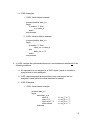
i. VHDL- latch inferred example
process (enable, data_in)
begin
If enable = ‘1’ then
q <= data_in;
end if;
end process;
ii. VHDL- latch avoidance example
process (enable, data_in)
begin
If enable = ‘1’ then
data_out <= data_in;
else
data_out <= ‘0’;
end if;
end process;
5. In VHDL, latches are synthesized whenever a case statement satisfies all of the
following conditions.
a. An expression is not assigned to a VHDL object (signal or variable) in
every branch of case statement.
b. VHDL objects assigned an expression in any case branch are not
assigned a value before the case statement is entered.
c. VHDL Examples.
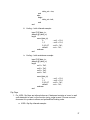
i. VHDL- latch inferred example
process (data_in)
begin
case data _in is
when 0
when 1 | 3
when 4 to 7 | 2
when others
end case;
=> out_1 <= ‘1’;
=> out_2 <= ‘1’;
=> out_3 <= ‘1’;
=> out_4 <= ‘1’;
15
end process;
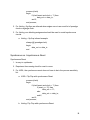
ii. VHDL- latch avoidance example
process (data_in)
begin
out_1 <= ‘0’;
out_2 <= ‘0’;
out_3 <= ‘0’;
out_4 <= ‘0’;
case data _in is
when 0
when 1 | 3
when 4 to 7 | 2
when others
end case;
end process;
=> out_1 <= ‘1’;
=> out_2 <= ‘1’;
=> out_3 <= ‘1’;
=> out_4 <= ‘1’;
6. In Verilog, latches are synthesized for a variable when all the following
statements are true.
a. Assignment to the variable occurs in at least one but not all of the
branches of a Verilog control statement.
b. Assignment to the variable does not occur on a clock’s edge.
c. Verilog Examples.
i. Verilog – latch inferred example
always @ (enable or data)
begin
if (enable)
begin
Q= data;
end
end
ii. Verilog – latch avoidance example
always @ (enable or ina or inb)
begin
if (enable)
begin
16
data_out = ina;
end
else
begin
data_out =inb;
end
end
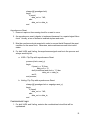
iii. Verilog – latch inferred example
input [3:0] data_in;
always @ (data_in)
begin
case (data_in)
0
1,3
2,4,5,6,7
default
endcase
end
: out1 = 1’b1;
: out2 = 1’b1;
:out3 = 1’b1;
:out = 1’b1;
iv. Verilog – latch avoidance example
input [3:0] data_in;
always @ (data_in)
begin
out1 = 1’b0;
out2 = 1’b0;
out3 = 1’b0;
out4 = 1’b0;
case (data_in)
0
1,3
2,4,5,6,7
default
endcase
: out1 = 1’b1;
: out2 = 1’b1;
:out3 = 1’b1;
:out = 1’b1;
end
Flip-Flops
1. For VHDL, flip-flops are inferred when an if statement contains a ‘event, a wait
until statement is used, or the function rising_edge is used. Choose one and
document it to produce uniform and professional looking code.
a. VHDL- flip-flop inferred example
17
process (clock)
begin
if (clock’event and clock = ‘1’) then
data_out <= data_in;
end if;
end process;
2. For Verilog , flip-flops are inferred when edges occur in an event list of posedge
clock or negedge clock.
3. For Verilog, non-blocking assignments should be used to model synchronous
circuits.
a. Verilog – flip flop inferred example
always @ (posedge clock)
begin
data_out <= data_in
end
Synchronous vs. Asynchronous Reset
Synchronous Reset
1. Is easy to synthesize.
2. Requires a free-running clock for reset to occur.
3. For VHDL, the synchronous reset does not have to be in the process sensitivity
list.
a. VHDL- Flip Flop with synchronous Reset
process (clock)
begin
if (clock’event and clock = ‘1’) then
if (reset_n = ‘0’) then
data_out <= ‘0’;
else
data_out <= data_in;
end if;
end if;
end process;
b. Verilog- Flip Flop with synchronous Reset
18
always @ (posedge clock)
begin
if (reset)
data_out <= 1’b0;
else
data_out <= data_in;
end
Asynchronous Reset
1. Does not require a free-running clock for a reset to occur
2. An asynchronous reset is harder to implement because it is a special signal like a
clock. Usually, a tree of buffers is inserted at place and route.
3. Must be synchronously de-asserted in order to ensure that all flops exit the reset
condition on the same clock. Otherwise, state machines can reset into invalid
states.
4. For both VHDL and Verilog, the asynchronous signal must be in the process and
always sensitivity list.
a. VHDL- Flip Flop with asynchronous Reset
process (clock, reset_n)
begin
if (reset_n = ‘0’) then
data_out <= ‘0’;
elsif (clock’event and clock = ‘1’) then
data_out <= data_in;
end if;
end process;
b. Verilog- Flip Flop with asynchronous Reset
always @ (posedge clock or negedge reset_n)
begin
if (!reset)
data_out <= 1’b0;
else
data_out <= data_in;
end
Combinatorial Logic
1. For both VHDL and Verilog, envision the combinational circuit that will be
synthesized.
19
2. For both VHDL and Verilog, avoid combinational feedback that is the looping of
combinational processes.
3. For both VHDL and Verilog, when modeling purely combinational logic, ensure
signals are assigned in every branch of conditional signal assignments.
4. For both VHDL and Verilog, ensure the sensitivity list of process statements in
VHDL and the event list of always statements in Verilog are complete.
5. For VHDL, do not include the after clause in a signal assignment. This clutters
the code and makes it harder to read.
a. VHDL – after clause used
C <= a and b after 10ns;
b. VHDL – after clause removed
C <= a and b;
6. For Verilog, do not include delays in assignment statements.
a. Verilog – Delay used
assign #10 c = a & b;
b. Verilog – Delay not included
assign c = a & b;
7. For Verilog, the always statement is supported by synthesis. The initial
statement is not.
Sensitivity Lists
1. Specify complete sensitivity lists in each of your process VHDL statements and
Verilog always blocks. If you don’t use a complete sensitivity list, the behavior of
the pre-synthesis design may differ from the post-synthesis netlist.
2. For sequential blocks, the sensitivity list must include the clock signal that is read
by the block. If the sequential block uses a reset signal, include the reset signal
in the sensitivity list.
a. VHDL example
seq_example: process (clk)
20
begin
if (clk’event and clk = ‘1’) then
a <= d;
end if ;
b. Verilog example
always @ (posedge clk)
begin
q <= d;
end
3. For combinational blocks, the sensitivity list must include every signal that is read
by the process.
a. VHDL example
comb_ex: process (a, b)
begin
if (b = ‘0’) then
sum <= a + 1;
else
sum <= a –1;
end if;
end process;
b. Verilog example
always @ (a or b)
begin
if (b == 0)
sum = a + 1;
else
sum = a – 1;
end
4. Verify that your process sensitivity lists contain only the necessary signals. Extra
signals add fat to the code, makes the code harder to read, and can slow down
simulations.
Block vs. Non-blocking
1. Verilog only. Blocking assignments execute in sequential order, non-blocking
assignments execute concurrently. When writing synthesizable code use non-
21
blocking assignments in always @ (posedge clock) blocks. Otherwise, the
simulation behavior of the HDL and gate_level designs may differ.
Signal vs. variable
1. VHDL only. During simulations, signal assignments are scheduled for execution
in the next simulation cycle. Variable assignments take effect immediately, and
they take place in the order in which they appear in code. When writing
synthesizeable code, use signals instead of variables to ensure that the
simulation behavior of the pre-synthesis design matches post-synthesis netlist.
Case vs. if-then-else
1. For VHDL and Verilog, a case statement infers a single-level multiplexer while an
if-then-else statement infers a priority-encoded, cascaded combination of
multiplexers. A mux is a faster circuit. If the priority-encoding structure is not
required use the case statement rather than if-then-else statement.
2. For VHDL and Verilog, for combinational logic from a case statement, ensure
that either default outputs are assigned immediately before the case statement or
that the outputs are always assigned regardless of which branch is taken through
the case statement. This will avoid latches being inferred. The others in VHDL
default case branch are optional to ensure all branch values are covered. The
default in Verilog case branch is essential to ensure all branch values are
covered and avoid inferring latches.
3. For VHDL, use case statements in preference to if statements containing else-if
clauses where applicable for efficient synthesized circuits. The if statement
operates on a priority encoded basis.
Case sensitivity
1. Remember, Verilog is case sensitive while VHDL is not. So in Verilog “A” and “a”
are different, while in VHDL they are treated as the same.
Bus Widths
1. In Verilog you have the freedom of assigning signals of different width to each
other. Therefore, be diligent to check this since Verilog compilers can’t detect
unintentional bit width mismatches. If widths do not match, either bits are
chopped off or extra bits are filed with logic 0.
22
Wait Until vs. If vs. Rising Edge
1. In VHDL, both the ‘if’’ and ‘wait until’ statements will infer flops. The ‘wait’
statement delays the execution of the whole process until its expression
becomes true. This means that all other signal assignments in the process will
infer one or more flops depending on the signal’s bit width. The ‘if’ statement
does not stop the execution of the whole process so it does not prohibit separate
purely combinational logic from also being modeled in the same process. For this
reason the ‘if ‘statement is preferred over the wait statement. In addition, using
the ‘if’ statement provides greater control over the inferred registers.
a. VHDL Example
wait until (clock’event and clock = ‘1’);
if (clock’event and clock = ‘1’) then
2. In VHDL, if you are using the IEEE std_logic_1164 package, you can use the
functions rising_edge and falling_edge to infer a flip-flop. The use of function
calls can simplify a model slightly especially if you’re using multi-valued data
types, like for example std_logic, that has nine possible values, (U, X, 0, 1, Z, W,
L, H, -). The reason the model is simplified is that in order to detect a rising edge
(logic 0 to 1 transition) for a signal type of std_logic, it is necessary to ensure
transitions like X to 1 are not detected.
a. VHDL Example
Clock is of type std_logic.
-- Attribute ‘event detects X to 0 and X to 1 transitions
if (clock’event and clock =’1’) then
-- Detects X to 1 transition
-- Detects only logic 0 to logic 1 transition
if rising_edge(clock) then
Partitioning for synthesis
I bet you’re already partitioning your design and may not know it. Lets say you’re
getting ready for a design review. You start drawing block diagrams. You may have a
top-level block showing all the I/O and inside the top-level block smaller blocks. These
smaller blocks may represent design functions for example an interface to a processor,
a clock generation block, or an encoding block. This is great for a design reviews. Each
sub-block might represent a particular design requirement. As you start describing each
block, the requirements as you have interpreted them are presented and perhaps
modified. Most reviewers like this methodology because they are only interested in
23
knowing that you understand the requirements and how are you going to meet the
requirements.
However, for synthesis, you might need to combine or break up these smaller blocks.
This combining or breaking up of blocks is what I’m calling partitioning for synthesis.
Correct design partitioning can enhance the synthesis results, reduce compile time,
and simplify the constraint and script files. Partitioning affects block size. If you make
blocks too small, you can create artificial boundaries that restrict effective optimization.
If you create very large blocks, compile runtimes can be lengthy. The following sections
cover guidelines to help improve optimization and runtimes.
Design Reuse
If you know some of your design may need to be reused consider the following items
when you start partitioning the design.
1. Thoroughly define and document the design interface.
2. Standardize interfaces whenever possible.
3. Parameterize the HDL code.
Related Combinatorial Logic
By default, Design Compiler can’t move logic across hierarchical boundaries during
compile. So if you separate related logic into different blocks you’ll create artificial
barriers that restrict logic optimization. By keeping related logic together Design
Compiler will have more flexibility in optimizing the design. Follow these suggestions
when partitioning your combinatorial logic.
1. Group related combinational logic and its destination register together.
2. Eliminate glue logic.
Register Block Outputs
Take the time to think about the outputs of each of your blocks. If an output can’t be
registered consider moving the logic into the block so that it can be registered.
Registering the output signals from each block simplifies the synthesis process.
1. For each block of a hierarchical design, register all output signals from the block.
24
Design goals
If at all possible, separate modules that have different design goals (speed, area, etc).
By doing so, Design Compiler can optimize critical path’s logic for speed, while
optimizing the non-critical path for logic area.
1. Keep critical path logic in a separate module from non-critical path logic.
Sharable Resources
Design compiler has the capability to share resources. To take advantage of this
feature, consider the following.
1. Place sharable resources in the same block. Design Compiler can share these
resources but only if the resources belong to the same VHDL process or Verilog
always block.
Isolating Special Functions
Try to isolate different function like I/O pads, asynchronous logic, and clock generation
circuitry. Isolation of the clock generation circuitry enables instantiation and careful
simulation of this module. Isolation of the asynchronous logic helps confine testability
problems and static timing analysis problems to a small area.
1. Isolate special functions (such as I/O pads, clock generation circuitry, boundaryscan logic, and asynchronous logic) from the core logic.
LEDA
The program has decided to use LEDA. Now what! The first step is to get a copy of the
LEDA user manual. This manual spells out in detail how to use LEDA. In this paper, I’ll
briefly describe what LEDA is, how does it work, and guidelines.
What is LEDA?
The LEDA tool is a programmable HDL checker that verifies that HDL code complies
with design rule and coding-style guidelines. By using the tool you can quickly verify
that the team has followed all the guidelines you’ve put into place.
LEDA consists of two separate tools: Specifier and Checker. The Specifier tool is used
to program/compile rules and exports policies to configure checkers. The checker tool
is used to verify code against different policies and generate error reports.
25
How does LEDA Work?
There are three types of rules in LEDA: language based, hardware based, and chiplevel rules. The Language-based rules constrain different HDL constructs by ensuring
that they correspond to acceptable values, ranges, or templates.
The hardware-based rules control the hardware semantics of VHDL and Verilog. Using
hardware-based rules, you can check for the proper use of clocks, and inferred
hardware such as latches, flip-flops, and finite state machines.
The chip-level rules work on the entire design hierarchy. For chip-level rules to work,
you must specify a top module in the design hierarchy. You can write chip-level rules
using templates (design, connectivity, test signal, and etc,).
Once you have programmed a set of rules, the LEDA Specifier compiles the rule source
code into an object format readable by the LEDA Checker. The Checker then compares
the input HDL code to the rules contained within the object files and outputs error
messages depending on whether the comparisons pass or fail.
LEDA Guidelines
Getting Started
1. There are three flows available for using LEDA. Determine which flow best suits
your team needs.
a. Configure the prepackage rules to meet all your needs.
b. Find a prepackage rule that is close to your needs. Copy the rules and
modify them.
c. Write all new rules because none of the prepackage rules meet your
needs.
2. Now that the flow has been selected you need to read in the design. For a
VHDL design, you can specify the location of the design files and the checker will
automatically figure out design dependencies and read the files in the right order.
For a Verilog design, you can use your simulation setup file with some very minor
changes.
3. If you need to modify the rules, the LEDA checkers include a rule-configuration
wizard to aid in selecting and configuring the different rules you want to check.
By using the GUI, you can turn rules on/off, set the severity-level, and configure
different rule-parameters.
26
4. Before you can use LEDA to test your HDL source code against the prepackaged
rules or new rules that you built, you must first create a project file. A project file
organizes your VHDL or Verilog source files into easily managed units.
5. To execute the checker, all you have to do is click of a button in the GUI, or use a
single command in the command-line.
6. After the checker is done you’ll get a list of violations. Decide how you want to
review the violations by complete design or individual units in the design. Once
you have isolated the list of violations that you intend to work on, the checker’s
cross-linked browser will enable you to easily jump from error to the
Verilog/VHDL code causing the violation or from the code back to the error.
General Guidelines
1. VHDL code must respect one of two standards: VHDL 87 or VHDL 93.
2. For both VHDL and Verilog, make sure you can analyze or compile the code.
3. For mixed-language designs make sure to resolve naming issues, since VHDL is
not case-sensitive and Verilog is case-sensitive. For example,
a. VHDL stores identifiers in upper case.
b. Verilog stores identifiers exactly as they appear in the source code,
regardless of case.
4. You can instantiate a Verilog module inside a VHDL architecture using a
component instantiation statement.
5. You can instantiate a VHDL entity, VHDL design entity, or VHDL configuration in
a Verilog module using a module instantiation statement.
6. LEDA supports Verilog 2001 constructs. See the user guide for the constructs
supported.
7. Be aware of the naming conventions for rule sets for VHDL and Verilog. Rule
sets are stored as ASCII text in ruleset.rl files for VHDL or ruleset.sl files for
Verilog.
27