1
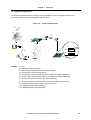
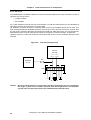
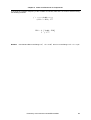
Preliminary User’s Manual IE-703242-G1-EM1 In-Circuit Emulator Option Board for V850ES/GB1 Hardware Document No. U16345EE1V0UM00 Date Published July 2002 NEC Corporation 2002 Printed in Germany NOTES FOR CMOS DEVICES 1 PRECAUTION AGAINST ESD FOR SEMICONDUCTORS Note: Strong electric field, when exposed to a MOS device, can cause destruction of the gate oxide and ultimately degrade the device operation. Steps must be taken to stop generation of static electricity as much as possible, and quickly dissipate it once, when it has occurred. Environmental control must be adequate. When it is dry, humidifier should be used. It is recommended to avoid using insulators that easily build static electricity. Semiconductor devices must be stored and transported in an anti-static container, static shielding bag or conductive material. All test and measurement tools including work bench and floor should be grounded. The operator should be grounded using wrist strap. Semiconductor devices must not be touched with bare hands. Similar precautions need to be taken for PW boards with semiconductor devices on it. 2 HANDLING OF UNUSED INPUT PINS FOR CMOS Note: No connection for CMOS device inputs can be cause of malfunction. If no connection is provided to the input pins, it is possible that an internal input level may be generated due to noise, etc., hence causing malfunction. CMOS devices behave differently than Bipolar or NMOS devices. Input levels of CMOS devices must be fixed high or low by using a pull-up or pull-down circuitry. Each unused pin should be connected to V DD or GND with a resistor, if it is considered to have a possibility of being an output pin. All handling related to the unused pins must be judged device by device and related specifications governing the devices. 3 STATUS BEFORE INITIALIZATION OF MOS DEVICES Note: Power-on does not necessarily define initial status of MOS device. Production process of MOS does not define the initial operation status of the device. Immediately after the power source is turned ON, the devices with reset function have not yet been initialized. Hence, power-on does not guarantee out-pin levels, I/O settings or contents of registers. Device is not initialized until the reset signal is received. Reset operation must be executed immediately after power-on for devices having reset function. 2 Preliminary User’s Manual U16345EE1V0UM00 MS-DOS and MS-Windows are either registered trademarks or trademarks of Microsoft Corporation in the United States and/or other countries. PC/AT and PC DOS are trademarks of IBM Corp. The related documents in this publication may include preliminary versions. However, preliminary versions are not marked as such. The export of this product from Japan is regulated by the Japanese government. To export this product may be prohibited without governmental license, the need for which must be judged by th customer. The export or re-export of this product from a country other than Japan may also be prohibited without a license from that country. Please call an NEC sales representative. The information in this document is current as of 30.07.2002. The information is subject to change without notice. For actual design-in, refer to the latest publications of NEC’s data sheets or data books, etc., for the most up-to-date specifications of NEC semiconductor products. Not all products and/or types are available in every country. Please check with an NEC sales representative for availability and additional information. No part of this document may be copied or reproduced in any form or by any means without prior written consent of NEC. NEC assumes no responsibility for any errors that may appear in this document. NEC does not assume any liability for infringement of patents, copyrights or other intellectual property rights of third parties by or arising from the use of NEC semiconductor products listed in this document or any other liability arising from the use of such products. No license, express, implied or otherwise, is granted under any patents, copyrights or other intellectual property rights of NEC or others. Descriptions of circuits, software and other related information in this document are provided for illustrative purposes in semiconductor product operation and application examples. The incorporation of these circuits, software and information in the design of customer’s equipment shall be done under the full responsibility of customer. NEC assumes no responsibility for any losses incurred by customers or third parties arising from the use of these circuits, software and information. While NEC endeavours to enhance the quality, reliability and safety of NEC semiconductor products, customers agree and acknowledge that the possibility of defects thereof cannot be eliminated entirely. To minimize risks of damage to property or injury (including death) to persons arising from defects in NEC semiconductor products, customers must incorporate sufficient safety measures in their design, such as redundancy, fire-containment and antifailure features. NEC semiconductor products are classified into the following three quality grades: “Standard”, “Special” and “Specific”. The “Specific” quality grade applies only to semiconductor products developed based on a customer-designated “quality assurance program” for a specific application. The recommended applications of a semiconductor product depend on its quality grade, as indicated below. Customers must check the quality grade of each semiconductor product before using it in a particular application. "Standard": Computers, office equipment, communications equipment, test and measurement equipment, audio and visual equipment, home electronic appliances, machine tools, personal electronic equipment and industrial robots. "Special": Transportation equipment (automobiles, trains, ships, etc.), traffic control systems, antidisaster systems, anti-crime systems, safety equipment and medical equipment (not specifically designed for life support). "Specific": Aircrafts, aerospace equipment, submersible repeaters, nuclear reactor control systems, life support systems or medical equipment for life support, etc. The quality grade of NEC semiconductor products is “Standard“ unless otherwise expressly specified in NEC's data sheets or data books, etc. If customers wish to use NEC semiconductor products in applications not intended by NEC, they must contact an NEC sales representative in advance to determine NEC's willingness to support a given application. Notes: (1) “NEC” as used in this statement means NEC Corporation and also includes its majority-owned subsidiaries. (2) “NEC semiconductor products” means any semiconductor product developed or manufactured by or for NEC (as defined above). M5 2000.03 Preliminary User’s Manual U16345EE1V0UM00 3 Regional Information Some information contained in this document may vary from country to country. Before using any NEC product in your application, please contact the NEC office in your country to obtain a list of authorized representatives and distributors. They will verify: • Device availability • Ordering information • Product release schedule • Availability of related technical literature • Development environment specifications (for example, specifications for third-party tools and components, host computers, power plugs, AC supply voltages, and so forth) • Network requirements In addition, trademarks, registered trademarks, export restrictions, and other legal issues may also vary from country to country. NEC Electronics Inc. (U.S.) Santa Clara, California Tel: 408-588-6000 800-366-9782 Fax: 408-588-6130 800-729-9288 NEC Electronics (Europe) GmbH Duesseldorf, Germany Tel: 0211-65 03 01 Fax: 0211-65 03 327 Sucursal en España Madrid, Spain Tel: 091- 504 27 87 Fax: 091- 504 28 60 Succursale Française Vélizy-Villacoublay, France Tel: 01-30-67 58 00 Fax: 01-30-67 58 99 Filiale Italiana Milano, Italy Tel: 02-66 75 41 Fax: 02-66 75 42 99 NEC Electronics Hong Kong Ltd. Hong Kong Tel: 2886-9318 Fax: 2886-9022/9044 Branch The Netherlands Eindhoven, The Netherlands Tel: 040-244 58 45 Fax: 040-244 45 80 NEC Electronics Hong Kong Ltd. Seoul Branch Seoul, Korea Tel: 02-528-0303 Fax: 02-528-4411 Branch Sweden Taeby, Sweden Tel: 08-63 80 820 Fax: 08-63 80 388 United Kingdom Branch Milton Keynes, UK Tel: 01908-691-133 Fax: 01908-670-290 NEC Electronics Singapore Pte. Ltd. Singapore Tel: 65-253-8311 Fax: 65-250-3583 NEC Electronics Taiwan Ltd. Taipei, Taiwan Tel: 02-2719-2377 Fax: 02-2719-5951 NEC do Brasil S.A. Electron Devices Division Guarulhos, Brasil Tel: 55-11-6465-6810 Fax: 55-11-6465-6829 4 Preliminary User’s Manual U16345EE1V0UM00 Table of Contents Chapter 1 1.1 1.2 1.3 1.4 1.5 1.6 1.7 1.8 Chapter 2 Overview . . . . . . . . . . . . . . . . . . . . . . . . . . . . . . . . . . . . . . . . . . . . . . . . . . . . . 11 Hardware Configuration . . . . . . . . . . . . . . . . . . . . . . . . . . . . . . . . . . . . . . . . . . . . . . . . . 11 Components of the Emulation System . . . . . . . . . . . . . . . . . . . . . . . . . . . . . . . . . . . . . 12 Features (When Connected to IE-V850ES-G1) . . . . . . . . . . . . . . . . . . . . . . . . . . . . . . . 13 Function Specifications (When Connected to IE-V850ES-G1) . . . . . . . . . . . . . . . . . . 14 System Configuration. . . . . . . . . . . . . . . . . . . . . . . . . . . . . . . . . . . . . . . . . . . . . . . . . . . 15 Package Contents . . . . . . . . . . . . . . . . . . . . . . . . . . . . . . . . . . . . . . . . . . . . . . . . . . . . . . 16 Connection between IE-V850ES-G1 and IE-703242-G1-EM1. . . . . . . . . . . . . . . . . . . . 17 Power up sequence . . . . . . . . . . . . . . . . . . . . . . . . . . . . . . . . . . . . . . . . . . . . . . . . . . . . 17 Name and Functions of Components. . . . . . . . . . . . . . . . . . . . . . . . . . . . . . 19 2.1 2.2 2.3 Name and Functions of IE-703242-G1-EM1 Components . . . . . . . . . . . . . . . . . . . . . . 19 Status LEDs . . . . . . . . . . . . . . . . . . . . . . . . . . . . . . . . . . . . . . . . . . . . . . . . . . . . . . . . . . . 21 Jumper Settings . . . . . . . . . . . . . . . . . . . . . . . . . . . . . . . . . . . . . . . . . . . . . . . . . . . . . . . 22 2.3.1 Overview . . . . . . . . . . . . . . . . . . . . . . . . . . . . . . . . . . . . . . . . . . . . . . . . . . . . . . . . . 22 2.3.2 Jumper JP2: AVDD selection. . . . . . . . . . . . . . . . . . . . . . . . . . . . . . . . . . . . . . . . . . 22 2.3.3 Jumper JP3: AVSS selection. . . . . . . . . . . . . . . . . . . . . . . . . . . . . . . . . . . . . . . . . . 23 2.4 Main Sockets and Connectors. . . . . . . . . . . . . . . . . . . . . . . . . . . . . . . . . . . . . . . . . . . . 24 2.4.1 Main Sockets . . . . . . . . . . . . . . . . . . . . . . . . . . . . . . . . . . . . . . . . . . . . . . . . . . . . . 24 2.4.2 Clock Connectors . . . . . . . . . . . . . . . . . . . . . . . . . . . . . . . . . . . . . . . . . . . . . . . . . . 24 2.4.3 Other Components . . . . . . . . . . . . . . . . . . . . . . . . . . . . . . . . . . . . . . . . . . . . . . . . . 24 2.5 Clock Operation . . . . . . . . . . . . . . . . . . . . . . . . . . . . . . . . . . . . . . . . . . . . . . . . . . . . . . . 25 2.5.1 Main Clock . . . . . . . . . . . . . . . . . . . . . . . . . . . . . . . . . . . . . . . . . . . . . . . . . . . . . . . 25 2.5.2 Sub Clock . . . . . . . . . . . . . . . . . . . . . . . . . . . . . . . . . . . . . . . . . . . . . . . . . . . . . . . . 26 Chapter 3 3.1 3.2 3.3 3.4 3.5 Chapter 4 4.1 4.2 4.3 4.4 4.5 4.6 4.7 Operating Precautions . . . . . . . . . . . . . . . . . . . . . . . . . . . . . . . . . . . . . . . . . . 29 Reset source monitor flag . . . . . . . . . . . . . . . . . . . . . . . . . . . . . . . . . . . . . . . . . . . . . . . 29 Standby release . . . . . . . . . . . . . . . . . . . . . . . . . . . . . . . . . . . . . . . . . . . . . . . . . . . . . . . 29 Port direction setting for peripheral function. . . . . . . . . . . . . . . . . . . . . . . . . . . . . . . . 29 Programmable peripheral area . . . . . . . . . . . . . . . . . . . . . . . . . . . . . . . . . . . . . . . . . . . 29 Other precautions . . . . . . . . . . . . . . . . . . . . . . . . . . . . . . . . . . . . . . . . . . . . . . . . . . . . . . 29 Differences between Target Device and Emulation Board. . . . . . . . . . . . . 31 BCU (bus control unit) . . . . . . . . . . . . . . . . . . . . . . . . . . . . . . . . . . . . . . . . . . . . . . . . . . 31 Load on voltage supply pins . . . . . . . . . . . . . . . . . . . . . . . . . . . . . . . . . . . . . . . . . . . . . 31 Reset input . . . . . . . . . . . . . . . . . . . . . . . . . . . . . . . . . . . . . . . . . . . . . . . . . . . . . . . . . . . 31 REGC pin . . . . . . . . . . . . . . . . . . . . . . . . . . . . . . . . . . . . . . . . . . . . . . . . . . . . . . . . . . . . . 31 Clock oscillator inputs . . . . . . . . . . . . . . . . . . . . . . . . . . . . . . . . . . . . . . . . . . . . . . . . . . 31 VPP pin . . . . . . . . . . . . . . . . . . . . . . . . . . . . . . . . . . . . . . . . . . . . . . . . . . . . . . . . . . . . . . . 31 AVDD, AVSS pins . . . . . . . . . . . . . . . . . . . . . . . . . . . . . . . . . . . . . . . . . . . . . . . . . . . . . . . 32 Appendix A Mechanical Data . . . . . . . . . . . . . . . . . . . . . . . . . . . . . . . . . . . . . . . . . . . . . . . 35 Appendix B Index . . . . . . . . . . . . . . . . . . . . . . . . . . . . . . . . . . . . . . . . . . . . . . . . . . . . . . . . 37 Preliminary User’s Manual U16345EE1V0UM00 5 6 Preliminary User’s Manual U16345EE1V0UM00 List of Figures Figure 1-1: Figure 1-2: Figure 2-1: Figure 2-2: Figure 2-3: Figure 2-4: Figure 2-5: Figure A-1: IE-703242-G1-EM1 hardware configuration................................................................ 11 System Configuration .................................................................................................. 15 IE-703242-G1-EM1 (top view)..................................................................................... 19 IE-703242-G1-EM1 (bottom view)............................................................................... 20 LEDs controlled by IE-703242-G1-EM1 ...................................................................... 21 Main Clock Configuration ............................................................................................ 25 Sub Clock Configuration.............................................................................................. 26 Mechanical Data.......................................................................................................... 35 Preliminary User’s Manual U16345EE1V0UM00 7 8 Preliminary User’s Manual U16345EE1V0UM00 List of Tables Table 1-1: Table 1-2: Table 1-3: Table 2-1: Table 2-2: Table 2-3: Table 2-4: Table 2-5: Table 2-6: Table 4-1: Components of Emulation System ................................................................................ 12 Features of IE-703242-G1-EM1 ..................................................................................... 13 Functional Specifications of IIE-703242-G1-EM1........................................................... 14 LEDs controlled by IE-703242-G1-EM1 ......................................................................... 21 Component Overview .................................................................................................... 22 Jumper JP2 - AVDD selection ........................................................................................ 22 Jumper JP3 - AVSS selection ........................................................................................ 23 Main Sockets ................................................................................................................. 24 Clock Connectors .......................................................................................................... 24 Pin list according to their emulation location .................................................................. 32 Preliminary User’s Manual U16345EE1V0UM00 9 10 Preliminary User’s Manual U16345EE1V0UM00 Chapter 1 Overview The IE-703242-G1-EM1 is an option board for the IE-V850ES-G1 in circuit emulator. Using the IE-703242-G1-EM1 in conjunction with the IE-V850ES-G1, hardware and software developed for V850ES/GB1 can be debugged efficiently. This manual describes the basic setup procedure and configuration settings of the IE-V850ES-G1 when used together with IE-703242-G1-EM1. 1.1 Hardware Configuration Figure 1-1: IE-703242-G1-EM1 hardware configuration Additional Hardware Probe cable (SWEX-100SD1) General purpose extension probe cable for target connection Emulation board IE-703242-G1-EM1 For use as emulation system for V850ES/GB1 connect this board to the In-Circuit-Emulator IE-V850ES-G1 Additional Hardware In-Circuit-Emulator (IE-V850ES-G1) PC-Interface Card IE-70000-PCI-IF-A IE-70000-CD-IF-A For connection of the IE-V850ES-G1 to a PC. Insert to the respective expansion slot of the PC IE-70000-PCI-IF-A: for PCI socket IE-70000-CD-IF-A: for PCMCIA socket Preliminary User’s Manual U16345EE1V0UM00 11 Chapter 1 Overview 1.2 Components of the Emulation System For order codes of the components that may be used in an emulation system for V850ES/GB1 refer to the following table: Table 1-1: Component Components of Emulation System Order Code Comment In-Circuit-Emulator IE-V850ES-G1 Main board for CPU emulation and trace Notes 1, 2 Emulation board IE-703242-G1-EM1 Emulation board for V850ES/GB1 Notes 1, 2 Probe cable SWEX-100SD1 Probe cable for target connection Note 2 Probe to target connector NQPACK100SD Board socket for target connection (soldered on target board) Note 2 Probe to target connector YQPACK100SD Probe connection (fixed on NQPACK100SD) Note 2 Probe to target connector YQSOCKET100SDF Distance socket (optional) PC interface card IE-70000-PCI-IF-A PCI interface card for host connection Note 3 PC interface card IE-70000-CD-IF-A PCMCIA interface card for host connection Note 3 Network interface IE-70000-MC-SV3 Network interface for host connection Note 3 Notes: 1. Required for stand alone operation (no target connection) 2. Required for operation with target hardware 3. The interfaces are alternative, one is mandatory 12 Preliminary User’s Manual U16345EE1V0UM00 Chapter 1 Overview 1.3 Features (When Connected to IE-V850ES-G1) Table 1-2: Features of IE-703242-G1-EM1 Parameter Value Operation frequency max. 16 MHz (Main clock) Operation Temperature range 0 to +40°C Storage temperature range -15 to +60°C Environmental humidity range 10 - 80% RH Supply voltage +4.5 V to +5.5 V ± 5% Supply current < 300 mA Power dissipation < 1 W (@ 16 MHz) Weight < 300 g Dimensions Note 205 mm x 140 mm x 20 mm Note: Please refer to the appendix “Mechanical data”. Preliminary User’s Manual U16345EE1V0UM00 13 Chapter 1 Overview 1.4 Function Specifications (When Connected to IE-V850ES-G1) Table 1-3: Functional Specifications of IIE-703242-G1-EM1 Parameter Emulation memory capacity Coverage memory capacity for execution/pass detection Coverage memory capacity for memory access detection Coverage memory capacity for branching entry number counting Specification Internal ROM 1 MB User memory 4 MB Internal ROM 256 KB External memory 1 MB External memory 1 MB Internal ROM 256 KB External memory 1 MB Trace memory capacity 168 bits × 32 K frames Time measurement function On-chip timer: 3 External logic probe 8-bit external trace possible Event setting for trace/break possible Event break Step execute break Forced break Break function Caution: 14 Fail safe break • Illegal access to peripheral I/O • Access to guard space • Write to the ROM space Some of the functions may not be supported, depending on the debugger used. Preliminary User’s Manual U16345EE1V0UM00 Chapter 1 Overview 1.5 System Configuration The system configuration when connecting the IE-V850ES-G1 to the IE-703242-G1-EM1 and a personal computer (PC/AT or compatible) is shown below. Figure 1-2: <2> System Configuration <3> <1> <9> <8> <4> <10> Target system <5> <11> Target system <6> <7> Remark: <1>: PC <2>: Debugger (Sold separately) <3>: Device file (Included with the IE-703242-G1-EM1) <4>: PC interface board (Sold separately) <5>: PC interface cable (Included with the IE-V850ES-G1 [Sold separately]) <6>: Power supply cable (Included with the IE-V850ES-G1 [Sold separately]) <7>: In-circuit emulator (IE-V850ES-G1: Sold separately) <8>: In-circuit emulator emulation board (IE-703242-G1-EM1: This product) <9>: Extension probe (SWEX-100SD1: Sold separately) <10>: YQPACK100SD (Sold separately) <11>: NQPACK100SD (Sold separately) Preliminary User’s Manual U16345EE1V0UM00 15 Chapter 1 Overview 1.6 Package Contents The packing box contains the following items: (1) Hardware: 1 pcs. IE-703242-G1-EM1 1 pcs. Antistatic bag 6 sets Screws/washers (2) Documentation: 1 pcs. Read me IE-703242-G1-EM1 1 pcs. Operating precautions 1 pcs. Hardware tool registration card 1 pcs. Notification on internet software update provision 1 pcs. Read me first 1 pcs. User’s manual (3) Software: Device Files on Floppy Disk 16 Preliminary User’s Manual U16345EE1V0UM00 Chapter 1 Overview 1.7 Connection between IE-V850ES-G1 and IE-703242-G1-EM1 The procedure for connecting the IE-V850ES-G1 and the IE-703242-G1-EM1 is shown below. 1. 2. 3. 4. Disconnect the power from IE-V850-ES-G1. Remove the cover of the IE-V850ES-G1. Make jumper settings on main board of IE-V850ES-G1 as described in 2.3 Jumper Settings. Place the IE-703242-G1-EM1 over the main board of IE-V850ES-G1 so that the board connectors are in the correct position. 5. Press IE-703242-G1-EM1 carefully so that the connection to the main board is secured. 6. Fix the IE-703242-G1-EM1 to the main board using the screws delivered with the board. 7. If the tool is used with a target board for emulation connect the probe adapter (SWEX-100SD1) to the appropriate socket (SO2) of IE-703242-G1-EM1. 8. Close the cover of the IE-V850ES-G1. 9. Reconnect the power to the IE-V850ES-G1. 10. If the tool is used with a target board for emulation connect the target socket probe adapter to the emulation target (emulation target powered off). Cautions: 1. Connect carefully so as not to break or bend connector pins. 2. Take care to match pin 1 when connecting the probe adapter to the probe socket of IE-703242-G1-EM1. 1.8 Power up sequence Power on the emulation system first, then power on the target system. Preliminary User’s Manual U16345EE1V0UM00 17 [MEMO] 18 Preliminary User’s Manual U16345EE1V0UM00 Chapter 2 Name and Functions of Components This chapter describes the names and functions of the components of IE-703242-G1-EM1. Also jumpers and switches used for configuration of the tool are described here. 2.1 Name and Functions of IE-703242-G1-EM1 Components Figure 2-1: IE-703242-G1-EM1 (top view) Preliminary User’s Manual U16345EE1V0UM00 19 Chapter 2 Name and Functions of Components Figure 2-2: 20 IE-703242-G1-EM1 (bottom view) Preliminary User’s Manual U16345EE1V0UM00 Chapter 2 Name and Functions of Components 2.2 Status LEDs Some of the LEDs of IE-V850ES-G1 are controlled by IE-703242-G1-EM1 to output status information. Refer to the IE-V850ES-G1 User’s Manual for information on the LEDs controlled by the IE-V850ES-G1 itself. Figure 2-3: EXTD TRG 1 2 Remark: LEDs controlled by IE-703242-G1-EM1 LED1 LED2 LED3 LED4 LED5 12 1 For information about external trigger inputs and output refer to IE-V850ES-G1 User’s Manual. Table 2-1: LEDs controlled by IE-703242-G1-EM1 LED Colour Function 1 green Target reset 2 green Don’t care (internal use only) 3 green Don’t care (internal use only) 4 yellow Target power on Note 5 red Main Power on Note: See 2.4 Main Sockets and Connectors for target power switching. Preliminary User’s Manual U16345EE1V0UM00 21 Chapter 2 Name and Functions of Components 2.3 Jumper Settings This chapter describes the function of the jumpers used to configure the IE-703242-G1-EM1. 2.3.1 Overview The following table sums up the jumpers and connectors used to configure the IE-703242-G1-EM1 for the desired operation. Table 2-2: Component Component Overview Function Described in JP1 Select sub clock signal generated by timer circuit 2.4.2 Clock Connectors JP2 AVDD input voltage selection 2.3.2 Jumper JP2: AVDD selection JP3 AVSS input voltage selection 2.3.3 Jumper JP3: AVSS selection SO1 Socket for alternative main clock oscillator 2.4.2 Clock Connectors SO2 Socket for target connection 2.4.1 Main Sockets CN1, CN2, CN3 Connection to IE-V850ES-G1 emulator 2.4.1 Main Sockets CN6 Socket for main clock crystal and capacitors 2.4.2 Clock Connectors CN9 Socket for sub clock crystal and capacitors 2.4.2 Clock Connectors SW2 Internal use (don’t press) - SW3 Internal use (don’t press) - 2.3.2 Jumper JP2: AVDD selection This function is used to select the input signal for the AVDD pin of the I/O chip on the IE-703242-G1-EM1 emulation board. Table 2-3: Position 22 Jumper JP2 - AVDD selection Function 1-2 (default) Connect AVDD to target 2-3 Connect AVDD to internal buffered 5 V supply Preliminary User’s Manual U16345EE1V0UM00 Chapter 2 Name and Functions of Components 2.3.3 Jumper JP3: AVSS selection This function is used to select the input signal for the AVSS pin of the I/O chip on the IE-703242-G1-EM1 emulation board. Table 2-4: Jumper JP3 - AVSS selection Position Function 1-2 (default) Connect AVSS to target 2-3 Connect AVSS to GND Preliminary User’s Manual U16345EE1V0UM00 23 Chapter 2 Name and Functions of Components 2.4 Main Sockets and Connectors This chapter describes the main sockets and connectors of the IE-703242-G1-EM1. This includes sockets for connection to the IE-V850ES-G1 emulator and connections to a target board as well as connectors used for clock selection and configuration. 2.4.1 Main Sockets The main sockets described here are used for proper installation of the IE-703242-G1-EM1 in the IE-V850ES-G1 emulator and for connection of a target board when the emulator is connected to external hardware. Table 2-5: Socket Main Sockets Function SO2 Socket is used to connect probe adapter (SWEX-100SD1) when the In-Circuit-Emulator is connected to external target hardware CN1, CN2, CN3 Connection between the IE-703242-G1-EM1 and the IE-V850ES-G1 emulator 2.4.2 Clock Connectors These are used to configure clock oscillators of the IE-703226-G1-MC to run at the desired operation frequency. Table 2-6: Connector / Socket Clock Connectors Function CN6 Socket for main clock crystal and capacitors CN9 Socket for sub clock crystal and capacitors SO1 Socket for main clock oscillator to be used alternatively instead of CN6 JP1 Select sub clock signal generated by timer circuit (alternative to CN6) 2.4.3 Other Components Further connectors and test points are used for internal testing during production and maintenance and are not listed here. 24 Preliminary User’s Manual U16345EE1V0UM00 Chapter 2 Name and Functions of Components 2.5 Clock Operation This chapter describes the operation of the clock generation of IE-703242-G1-EM1. The V850ES/GB1 features two clock oscillators: a main clock oscillator for normal operation and a sub clock oscillator that allows to run the microcontroller at a slow operation speed to implement certain power save functions. 2.5.1 Main Clock The main clock oscillator of the V850ES/GB1 and also IE-703242-G1-EM1 operates at frequencies up to 16 MHz. On the emulation board the source for the main clock can either be a crystal or a dedicated C-MOS oscillator. By default a crystal is used which is assembled to the respective connector (CN6). Alternatively a dedicated C-MOS oscillator in DIL Package may be used. In this case the crystal and capacitors must be removed from CN6 and a crystal oscillator must be mounted to socket SO1. Figure 2-4: Main Clock Configuration Venus I/O chip X1 X2 SO1 CN6 Caution: Since the clock inputs X1 and X2 of the I/O chip are not connected to the target, crystal or oscillator operation from the target board is not possible. Crystal or Oscillator provided on the emulation board must be used. Preliminary User’s Manual U16345EE1V0UM00 25 Chapter 2 Name and Functions of Components 2.5.2 Sub Clock The V850ES/GB1 is available in different versions that feature different sub clock oscillators for device operation at low frequencies: • Crystal oscillator • RC oscillator If a crystal oscillator is used for the sub clock oscillator, a crystal of a fixed frequency of 32.768 KHz and capacitors must be connected to the connector CN9. For emulation of the RC oscillator a dedicated timer circuit on the emulation board can be used. This timer circuit generates an adjustable frequency in the range of 40 to 100 KHz. If the timer circuit is used the sub clock crystal and capacitors must be disconnected from CN9 and jumper JP1 must be shorted. By default the timer circuit is configured to operate at a frequency of about 100 KHz. To adjust the operating frequency of the sub clock timer circuit R28, R29 and C77 on the emulation board must be changed. Figure 2-5: Sub Clock Configuration Venus I/O chip CL1 (XT1) Oscillator Circuit CL2 (XT2) JP1 CN9 32.768 KHz Caution: 26 Since the clock inputs CL1 and CL2 (XT1 and XT2 respectively) are not connected to the target, crystal or RC oscillator operation from the target board is not possible. Crystal or RC oscillator provided on the emulation board must be used. Preliminary User’s Manual U16345EE1V0UM00 Chapter 2 Name and Functions of Components To change the operation frequency of the oscillator circuit R28, R29 and C77 must be selected using the following formulae: 1.44 f = ---------------------------------------------------( R28 + 2 ⋅ R29 ) ⋅ C77 1 1.44 - – R28 R29 = --- ⋅ -------------- 2 f ⋅ C77 Remark: Use R28 and R29 in the Range 1 KΩ < R < 10 MΩ and C77 in the Range 1 nF < C < 10 µF. Preliminary User’s Manual U16345EE1V0UM00 27 [MEMO] 28 Preliminary User’s Manual U16345EE1V0UM00 Chapter 3 Operating Precautions Be aware of the following operating precautions when using the IE-703242-G1-EM1. 3.1 Reset source monitor flag The reset source (reset caused by external reset input or watchdog timer) can not be distinguished by the RSM register of the clock controller during emulation mode. Oscillation stabilization time is skipped after a watchdog timer reset during sub watch mode. 3.2 Standby release The main oscillator of the V850ES/GB1 I/O chip on the emulation board is always running and can not be switched off. Therefore no oscillation stabilization time is required when stop mode or sub watch mode of V850ES/GB1 is released. As a consequence of this the V850ES/GB1 I/O chip on the ICE will wake up immediately from sub watch or stop mode whereas the V850ES/GB1 real chip always assures the oscillation stabilization time for the main oscillator when standby mode is released. 3.3 Port direction setting for peripheral function When a peripheral function is used the direction setting for the respective port bit of the V850ES/GB1 real chip is not set automatically. The port bit direction has to be programmed according to the requirement of the peripheral function by setting the port mode register. In the FPGA on the emulation board port mode setting is not necessary when a peripheral function is used. Therefore on the emulator ports emulated by the FPGA behave different from the real chip. This only affects bit 1 of port PCM, CLOCKOUT function. Therefore if the CLOCKOUT function is to be used the respective bit positions of registers PMCM and PMCCM have to be set accordingly. 3.4 Programmable peripheral area The usable settings for the BPC register limit usage to the first 32MB of the total address range. Therefore the programmable peripheral area must be set to an address range within the first 32 MB. 3.5 Other precautions Take note of the differences between the In-Circuit Emulator and the real chip described in Chapter 4 Differences between Target Device and Emulation Board. Preliminary User’s Manual U16345EE1V0UM00 29 [MEMO] 30 Preliminary User’s Manual U16345EE1V0UM00 Chapter 4 Differences between Target Device and Emulation Board When the In-Circuit-Emulator is connected to a target system for debugging, the V850ES/GB1 is emulated which means that the emulator behaves like the real chip in the target system. Small differences occur however. This chapter lists differences between the emulation system and the V850ES/GB1. 4.1 BCU (bus control unit) The BCU is established within an FPGA. Therefore this could be slightly different to the real chip. 4.2 Load on voltage supply pins The I/O chip is supplied by a power supply on the emulation board. Therefore the load on the power supply of the target board is very low compared to the real chip. 4.3 Reset input The reset pin of the target connector is not connected to the reset pin of the I/O chip directly. It also has got a 10 KΩ pull-up resistor connected to it. The input characteristic differs from the real chip. 4.4 REGC pin The REGC pin of the target connector is not connected to the corresponding pin of the I/O chip. On the emulation board a capacitor is connected to the REGC pin of the I/O chip internally. 4.5 Clock oscillator inputs The pins for main clock connection (X1 and X2) as well as the pins for sub clock connection (CL1, CL2 / XT1, XT2) of the I/O chip on the emulation board are not connected to the target connector. If a crystal is to be used for the clock generator it must be connected to the respective connector on the emulation board which is located electrically close to the I/O chip. Crystal operation from the target board is not possible. Alternatively a dedicated C-MOS oscillator can be used for the main clock and a timer circuit provided on the emulation board can be used for the sub clock (See also 2.5 Clock Operation). 4.6 VPP pin VPP pin of the I/O chip on the emulation board is connected to the target connector with a load of 10 KΩ (series resistor). On the emulation board it is only monitored and not used internally. Correct connection on the target board must be assured. Preliminary User’s Manual U16345EE1V0UM00 31 Chapter 4 Differences between Target Device and Emulation Board 4.7 AVDD, AVSS pins AVDD and AVSS pins of the I/O chip on the emulation board can be disconnected from the target connector. ADC values and the load on AVDD and AVSS pins may differ in that case. Table 4-1: 100 Pin 32 Top pin name Pin list according to their emulation location (1/3) Pin Function default I/O Emulated by single chip Venus chip Emulated by FPGA via Level Shifter Alternative connected to: 1 AVDD AVDD S Venus internal 2 AVSS AVSS S Venus internal 3 P00 P00/INTP0 I Venus 4 P01 P01/INTP1 I Venus 5 P02 P02/INTP2 I Venus 6 P03 P03/INTP3 I Venus 7 P04 P04/INTP4 I Venus 8 P05 P05/INTP5 I Venus 9 VDD50 VDD50 S buffered 10 REGC0 REGC0 S not connected 11 VSS30 VSS30 S Ground 12 X1 X1 I not connected 13 X2 X2 O not connected 14 RESET RESET I buffered 15 XT1 XT1 I not connected 16 XT2 XT2 O not connected 17 NMI NMI I Venus 18 P06 P06/INTP6 I Venus 19 P10 P10/SI00 I Venus 20 P11 P11/SO00 I Venus 21 P12 P12/SCK00 I Venus 22 P13 P13/RXD60/INTP7 I Venus 23 P14 P14/TXD60 I Venus 24 P15 P15 I Venus 25 P40 P40/KR0 I Venus 26 P41 P41/KR1/TIG00 I Venus 27 P42 P42/KR2/TIG01/TOG01 I Venus 28 P43 P43/KR3/TIG02/TOG02 I Venus 29 P44 P44/KR4/TIG03/TOG03 I Venus 30 P45 P45/KR5/TIG04/TOG04 I Venus 31 P46 P46/KR6/TIG05 I Venus 32 P47 P47/KR7 I Venus 33 P50 P50 I Venus Preliminary User’s Manual U16345EE1V0UM00 Chapter 4 Differences between Target Device and Emulation Board Table 4-1: 100 Pin Top pin name Pin list according to their emulation location (2/3) Pin Function default I/O Emulated by single chip Venus chip Emulated by FPGA via Level Shifter Alternative connected to: 34 P51 P51 I Venus 35 P52 P52 I Venus 36 P53 P53 I Venus 37 P54 P54/DCTXD0 I Venus 38 P55 P55/DCRXD0 I Venus 39 P56 P56 I Venus 40 P57 P57 I Venus 41 PCS0 PCS0 I FPGA via L/S 42 PCS1 PCS1 I FPGA via L/S 43 PDL0 PDL0 I FPGA via L/S 44 PDL1 PDL1 I FPGA via L/S 45 PDL2 PDL2 I FPGA via L/S 46 PDL3 PDL3 I FPGA via L/S 47 PDL4 PDL4 I FPGA via L/S 48 PDL5 PDL5 I FPGA via L/S 49 PDL6 PDL6 I FPGA via L/S 50 PDL7 PDL7 I FPGA via L/S 51 PDL8 PDL8 I FPGA via L/S 52 PDL9 PDL9 I FPGA via L/S 53 PDL10 PDL10 I FPGA via L/S 54 PDL11 PDL11 I FPGA via L/S 55 PDL12 PDL12 I FPGA via L/S 56 PDL13 PDL13 I FPGA via L/S 57 VPP VPP S 58 PDL14 PDL14 I FPGA via L/S 59 PDL15 PDL15 I FPGA via L/S 60 VDD51 VDD51 S buffered 61 VSS51 VSS51 S Ground 62 PCM0 PCM0 I FPGA via L/S 63 PCM1 PCM1, CLOCKOUT I FPGA via L/S 64 PCM2 PCM2 I FPGA via L/S 65 VSS31 VSS31 S Ground 66 REGC1 REGC1 S not connected 67 PCM3 PCM4 I FPGA via L/S 68 PDH0 PDH0 I FPGA via L/S 69 PDH1 PDH1 I FPGA via L/S 70 PDH2 PDH2 I FPGA via L/S 71 PDH3 PDH3 I FPGA via L/S 72 PDH4 PDH4 I FPGA via L/S not connected Preliminary User’s Manual U16345EE1V0UM00 33 Chapter 4 Differences between Target Device and Emulation Board Table 4-1: 100 Pin 34 Top pin name Pin list according to their emulation location (3/3) Pin Function default I/O Emulated by single chip Venus chip Emulated by FPGA via Level Shifter 73 PDH5 PDH5 I FPGA via L/S 74 PCT0 PCT0 I FPGA via L/S 75 PCT1 PCT1 I FPGA via L/S 76 PCT4 PCT4 I FPGA via L/S 77 PCT6 PCT6 I FPGA via L/S 78 P20 P20/RXD61/INTP8 I Venus 79 P21 P21/TXD61 I Venus 80 P22 P22/SI01 I Venus 81 P23 P23/SO01 I Venus 82 P24 P24/SCK01 I Venus 83 P25 P25 I Venus 84 P30 P30/TI50/TO50 I Venus 85 P31 P31/TI51/TO51 I Venus 86 P32 P32/TI52/TO52 I Venus 87 P33 P33/TIC00/TOC0 I Venus 88 P34 P34/TIC01 I Venus 89 P711 P711/ANI11 I Venus 90 P710 P710/ANI10 I Venus 91 P79 P79/ANI9 I Venus 92 P78 P78/ANI8 I Venus 93 P77 P77/ANI7 I Venus 94 P76 P76/ANI6 I Venus 95 P75 P75/ANI5 I Venus 96 P74 P74/ANI4 I Venus 97 P73 P73/ANI3 I Venus 98 P72 P72/ANI2 I Venus 99 P71 P71/ANI1 I Venus 100 P70 P70/ANI0 I Venus Preliminary User’s Manual U16345EE1V0UM00 Alternative connected to: Appendix A Figure A-1: Mechanical Data Mechanical Data Preliminary User’s Manual U16345EE1V0UM00 35 [MEMO] 36 Preliminary User’s Manual U16345EE1V0UM00 Appendix B Index A AVDD pin . . . . . . . . . . . . . . . . . . . . . . . . . . . . . . . . . . . . . . . . . . . . . . . . . . . . . . . . . . . . . . . . . . . . . . . 32 AVDD selection . . . . . . . . . . . . . . . . . . . . . . . . . . . . . . . . . . . . . . . . . . . . . . . . . . . . . . . . . . . . . . . . . . 22 AVSS pin . . . . . . . . . . . . . . . . . . . . . . . . . . . . . . . . . . . . . . . . . . . . . . . . . . . . . . . . . . . . . . . . . . . . . . . 32 AVSS selection . . . . . . . . . . . . . . . . . . . . . . . . . . . . . . . . . . . . . . . . . . . . . . . . . . . . . . . . . . . . . . . . . . 23 B BCU (bus control unit) . . . . . . . . . . . . . . . . . . . . . . . . . . . . . . . . . . . . . . . . . . . . . . . . . . . . . . . . . . . . . 31 BPC register . . . . . . . . . . . . . . . . . . . . . . . . . . . . . . . . . . . . . . . . . . . . . . . . . . . . . . . . . . . . . . . . . . . . . 29 C clock connectors . . . . . . . . . . . . . . . . . . . . . . . . . . . . . . . . . . . . . . . . . . . . . . . . . . . . . . . . . . . . . . . . . . . 24 main clock . . . . . . . . . . . . . . . . . . . . . . . . . . . . . . . . . . . . . . . . . . . . . . . . . . . . . . . . . . . . . . . . . . . 25 sub clock . . . . . . . . . . . . . . . . . . . . . . . . . . . . . . . . . . . . . . . . . . . . . . . . . . . . . . . . . . . . . . . . . . . . 26 clock oscillator inputs . . . . . . . . . . . . . . . . . . . . . . . . . . . . . . . . . . . . . . . . . . . . . . . . . . . . . . . . . . . . . . 31 CN1 . . . . . . . . . . . . . . . . . . . . . . . . . . . . . . . . . . . . . . . . . . . . . . . . . . . . . . . . . . . . . . . . . . . . . . . . . . . 24 CN2 . . . . . . . . . . . . . . . . . . . . . . . . . . . . . . . . . . . . . . . . . . . . . . . . . . . . . . . . . . . . . . . . . . . . . . . . . . . 24 CN3 . . . . . . . . . . . . . . . . . . . . . . . . . . . . . . . . . . . . . . . . . . . . . . . . . . . . . . . . . . . . . . . . . . . . . . . . . . . 24 CN6 . . . . . . . . . . . . . . . . . . . . . . . . . . . . . . . . . . . . . . . . . . . . . . . . . . . . . . . . . . . . . . . . . . . . . . . . . . . 24 CN9 . . . . . . . . . . . . . . . . . . . . . . . . . . . . . . . . . . . . . . . . . . . . . . . . . . . . . . . . . . . . . . . . . . . . . . . . . . . 24 configuration (hardware) . . . . . . . . . . . . . . . . . . . . . . . . . . . . . . . . . . . . . . . . . . . . . . . . . . . . . . . . . . . 11 connection emulation board to IE-V850ES-G1 . . . . . . . . . . . . . . . . . . . . . . . . . . . . . . . . . . . . . . . . . . . . . . . . 17 D differences . . . . . . . . . . . . . . . . . . . . . . . . . . . . . . . . . . . . . . . . . . . . . . . . . . . . . . . . . . . . . . . . . . . . . . 31 dimensions . . . . . . . . . . . . . . . . . . . . . . . . . . . . . . . . . . . . . . . . . . . . . . . . . . . . . . . . . . . . . . . . . . . . . . 13 E emulation board . . . . . . . . . . . . . . . . . . . . . . . . . . . . . . . . . . . . . . . . . . . . . . . . . . . . . . . . . . . . . . . . . . 12 F frequency (operation frequency) . . . . . . . . . . . . . . . . . . . . . . . . . . . . . . . . . . . . . . . . . . . . . . . . . . . . . 13 H humidity (environmental humidity) . . . . . . . . . . . . . . . . . . . . . . . . . . . . . . . . . . . . . . . . . . . . . . . . . . . . 13 I IE-70000-CD-IF-A . . . . . . . . . . . . . . . . . . . . . . . . . . . . . . . . . . . . . . . . . . . . . . . . . . . . . . . . . . . . . . . . 12 IE-70000-MC-SV3 . . . . . . . . . . . . . . . . . . . . . . . . . . . . . . . . . . . . . . . . . . . . . . . . . . . . . . . . . . . . . . . . 12 IE-70000-PCI-IF-A . . . . . . . . . . . . . . . . . . . . . . . . . . . . . . . . . . . . . . . . . . . . . . . . . . . . . . . . . . . . . . . . 12 IE-703242-G1-EM1 . . . . . . . . . . . . . . . . . . . . . . . . . . . . . . . . . . . . . . . . . . . . . . . . . . . . . . . . . . . . . . . 12 IE-V850ES-G1 . . . . . . . . . . . . . . . . . . . . . . . . . . . . . . . . . . . . . . . . . . . . . . . . . . . . . . . . . . . . . . . . . . . 12 In-Circuit-Emulator . . . . . . . . . . . . . . . . . . . . . . . . . . . . . . . . . . . . . . . . . . . . . . . . . . . . . . . . . . . . . . . . 12 interface network interface card . . . . . . . . . . . . . . . . . . . . . . . . . . . . . . . . . . . . . . . . . . . . . . . . . . . . . . . . . . 12 PC interface card . . . . . . . . . . . . . . . . . . . . . . . . . . . . . . . . . . . . . . . . . . . . . . . . . . . . . . . . . . . . . . 12 J JP1 . . . . . . . . . . . . . . . . . . . . . . . . . . . . . . . . . . . . . . . . . . . . . . . . . . . . . . . . . . . . . . . . . . . . . . . . . . . . 24 JP2 . . . . . . . . . . . . . . . . . . . . . . . . . . . . . . . . . . . . . . . . . . . . . . . . . . . . . . . . . . . . . . . . . . . . . . . . . . . . 22 JP3 . . . . . . . . . . . . . . . . . . . . . . . . . . . . . . . . . . . . . . . . . . . . . . . . . . . . . . . . . . . . . . . . . . . . . . . . . . . . 23 jumper settings . . . . . . . . . . . . . . . . . . . . . . . . . . . . . . . . . . . . . . . . . . . . . . . . . . . . . . . . . . . . . . . . . . . 22 Preliminary User’s Manual U16345EE1V0UM00 37 Appendix B Index L LED status . . . . . . . . . . . . . . . . . . . . . . . . . . . . . . . . . . . . . . . . . . . . . . . . . . . . . . . . . . . . . . . . . . . . . . . 21 M memory coverage . . . . . . . . . . . . . . . . . . . . . . . . . . . . . . . . . . . . . . . . . . . . . . . . . . . . . . . . . . . . . . . . . . . . 14 emulation . . . . . . . . . . . . . . . . . . . . . . . . . . . . . . . . . . . . . . . . . . . . . . . . . . . . . . . . . . . . . . . . . . . . 14 trace . . . . . . . . . . . . . . . . . . . . . . . . . . . . . . . . . . . . . . . . . . . . . . . . . . . . . . . . . . . . . . . . . . . . . . . . 14 N NQPACK100SD . . . . . . . . . . . . . . . . . . . . . . . . . . . . . . . . . . . . . . . . . . . . . . . . . . . . . . . . . . . . . . . . . . 12 O order code . . . . . . . . . . . . . . . . . . . . . . . . . . . . . . . . . . . . . . . . . . . . . . . . . . . . . . . . . . . . . . . . . . . . . . 12 oscillator crystal for sub clock . . . . . . . . . . . . . . . . . . . . . . . . . . . . . . . . . . . . . . . . . . . . . . . . . . . . . . . . . . . . 26 main clock . . . . . . . . . . . . . . . . . . . . . . . . . . . . . . . . . . . . . . . . . . . . . . . . . . . . . . . . . . . . . . . . . . . 25 RC for sub clock . . . . . . . . . . . . . . . . . . . . . . . . . . . . . . . . . . . . . . . . . . . . . . . . . . . . . . . . . . . . . . 26 P PCI interface card . . . . . . . . . . . . . . . . . . . . . . . . . . . . . . . . . . . . . . . . . . . . . . . . . . . . . . . . . . . . . . . . 12 PCMCIA interface card . . . . . . . . . . . . . . . . . . . . . . . . . . . . . . . . . . . . . . . . . . . . . . . . . . . . . . . . . . . . 12 pin list . . . . . . . . . . . . . . . . . . . . . . . . . . . . . . . . . . . . . . . . . . . . . . . . . . . . . . . . . . . . . . . . . . . . . . . . . . 32 precautions . . . . . . . . . . . . . . . . . . . . . . . . . . . . . . . . . . . . . . . . . . . . . . . . . . . . . . . . . . . . . . . . . . . . . 29 probe cable . . . . . . . . . . . . . . . . . . . . . . . . . . . . . . . . . . . . . . . . . . . . . . . . . . . . . . . . . . . . . . . . . . . . . 12 R REGC pin . . . . . . . . . . . . . . . . . . . . . . . . . . . . . . . . . . . . . . . . . . . . . . . . . . . . . . . . . . . . . . . . . . . . . . . 31 reset input pin . . . . . . . . . . . . . . . . . . . . . . . . . . . . . . . . . . . . . . . . . . . . . . . . . . . . . . . . . . . . . . . . . . . . . 31 RSM register . . . . . . . . . . . . . . . . . . . . . . . . . . . . . . . . . . . . . . . . . . . . . . . . . . . . . . . . . . . . . . . . . . . . 29 S settings clock settings . . . . . . . . . . . . . . . . . . . . . . . . . . . . . . . . . . . . . . . . . . . . . . . . . . . . . . . . . . . . . . . . . 25 jumper configuration . . . . . . . . . . . . . . . . . . . . . . . . . . . . . . . . . . . . . . . . . . . . . . . . . . . . . . . . . . . 22 SO1 . . . . . . . . . . . . . . . . . . . . . . . . . . . . . . . . . . . . . . . . . . . . . . . . . . . . . . . . . . . . . . . . . . . . . . . . . . . 24 SO2 . . . . . . . . . . . . . . . . . . . . . . . . . . . . . . . . . . . . . . . . . . . . . . . . . . . . . . . . . . . . . . . . . . . . . . . . . . . 24 specifications functional . . . . . . . . . . . . . . . . . . . . . . . . . . . . . . . . . . . . . . . . . . . . . . . . . . . . . . . . . . . . . . . . . . . . 14 standby release . . . . . . . . . . . . . . . . . . . . . . . . . . . . . . . . . . . . . . . . . . . . . . . . . . . . . . . . . . . . . . . . . . 29 status LED . . . . . . . . . . . . . . . . . . . . . . . . . . . . . . . . . . . . . . . . . . . . . . . . . . . . . . . . . . . . . . . . . . . . . . 21 supply current . . . . . . . . . . . . . . . . . . . . . . . . . . . . . . . . . . . . . . . . . . . . . . . . . . . . . . . . . . . . . . . . . . . . . . 13 voltage . . . . . . . . . . . . . . . . . . . . . . . . . . . . . . . . . . . . . . . . . . . . . . . . . . . . . . . . . . . . . . . . . . . . . . 13 SWEX-100SD1 . . . . . . . . . . . . . . . . . . . . . . . . . . . . . . . . . . . . . . . . . . . . . . . . . . . . . . . . . . . . . . . . . . 12 T temperature operation . . . . . . . . . . . . . . . . . . . . . . . . . . . . . . . . . . . . . . . . . . . . . . . . . . . . . . . . . . . . . . . . . . . . 13 storage . . . . . . . . . . . . . . . . . . . . . . . . . . . . . . . . . . . . . . . . . . . . . . . . . . . . . . . . . . . . . . . . . . . . . . 13 V view bottom view of emulation board . . . . . . . . . . . . . . . . . . . . . . . . . . . . . . . . . . . . . . . . . . . . . . . . . . . 20 top view of emulation board . . . . . . . . . . . . . . . . . . . . . . . . . . . . . . . . . . . . . . . . . . . . . . . . . . . . . . 19 VPP pin . . . . . . . . . . . . . . . . . . . . . . . . . . . . . . . . . . . . . . . . . . . . . . . . . . . . . . . . . . . . . . . . . . . . . . . . 31 38 Preliminary User’s Manual U16345EE1V0UM00 Appendix B Index W weight . . . . . . . . . . . . . . . . . . . . . . . . . . . . . . . . . . . . . . . . . . . . . . . . . . . . . . . . . . . . . . . . . . . . . . . . . . 13 Y YQPACK100SD . . . . . . . . . . . . . . . . . . . . . . . . . . . . . . . . . . . . . . . . . . . . . . . . . . . . . . . . . . . . . . . . . . 12 YQSOCKET100SD . . . . . . . . . . . . . . . . . . . . . . . . . . . . . . . . . . . . . . . . . . . . . . . . . . . . . . . . . . . . . . . 12 Preliminary User’s Manual U16345EE1V0UM00 39 40 Preliminary User’s Manual U16345EE1V0UM00 Facsimile Message From: Name Company Tel. Although NEC has taken all possible steps to ensure that the documentation supplied to our customers is complete, bug free and up-to-date, we readily accept that errors may occur. Despite all the care and precautions we've taken, you may encounter problems in the documentation. Please complete this form whenever you'd like to report errors or suggest improvements to us. FAX Address Thank you for your kind support. North America Hong Kong, Philippines, Oceania NEC Electronics Inc. NEC Electronics Hong Kong Ltd. Corporate Communications Dept. Fax: +852-2886-9022/9044 Fax: +1-800-729-9288 +1-408-588-6130 Korea Europe NEC Electronics Hong Kong Ltd. NEC Electronics (Europe) GmbH Seoul Branch Market Communication Dept. Fax: +82-2-528-4411 Fax: +49-211-6503-274 South America NEC do Brasil S.A. Fax: +55-11-6462-6829 Asian Nations except Philippines NEC Electronics Singapore Pte. Ltd. Fax: +65-250-3583 Japan NEC Semiconductor Technical Hotline Fax: +81- 44-435-9608 Taiwan NEC Electronics Taiwan Ltd. Fax: +886-2-2719-5951 I would like to report the following error/make the following suggestion: Document title: Document number: Page number: If possible, please fax the referenced page or drawing. Document Rating Excellent Good Acceptable Poor Clarity Technical Accuracy Organization CS 01.2