1
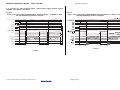
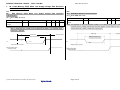
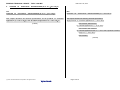
Date: Nov. 26, 2014 RENESAS TECHNICAL UPDATE 1753, Shimonumabe, Nakahara-ku, Kawasaki-shi, Kanagawa 211-8668 Japan Renesas Electronics Corporation Product Category Title MPU/MCU Document No. TN-RL*-A027B/E Correction for Incorrect Description Notice RL78/G12 Descriptions in the Hardware User’s Manual Rev. 2.00 Changed Information Category Technical Notification Reference Document RL78/G12 User’s Manual: Hardware Rev.2.00 R01UH0200EJ0200 (Aug. 2013) Rev. 2.00 Lot No. Applicable Product RL78/G12 R5F102xxx, R5F103xxx All lots This document describes misstatements found in the RL78/G12 User’s Manual: Hardware Rev.2.00 (R01UH0200EJ0200). Corrections Applicable Item CHAPTER 28 ELECTRICAL SPECIFICATIONS (A, D: TA = −40 to +85°C) CHAPTER 29 ELECTRICAL SPECIFICATIONS (G: TA = −40 to +105°C) Applicable Page Contents Page 732 Content change Page 778 Content change Document Improvement The above corrections will be made for the next revision of the User’s Manual: Hardware. (c) 2014. Renesas Electronics Corporation. All rights reserved. Page 1 of 16 RENESAS TECHNICAL UPDATE TN-RL*-$%(Date: Nov. 26, 2014 Corrections in the User’s Manual: Hardware No. 1 2 3 4 5 6 7 8 9 10 Corrections and Applicable Items Document No. English R01UH0200EJ0200 1.4 Pin Configuration (Top View) 1.4.2 24-pin products Pages 9 and 10 1.4.3 30-pin products 5.3.9 High-speed on-chip oscillator trimming Page 128 register (HIOTRM) 11.5.7 SNOOZE mode function Timing Chart of SNOOZE Mode Operation Pages 404 and 406 (Figure 11-71. and Figure 11-73.) 11.6.3 SNOOZE mode function Page 429 11.6.3 SNOOZE mode function Pages 431, 432 and Timing Chart of SNOOZE Mode Operation 434 (Figure 11-90., Figure 11-91. and Figure 11-93.) 19.2 Configuration of Power-on-reset Circuit Figure 19-2. Timing of Generation of Internal Page 639 Reset Signal by Power-on-reset Circuit and Voltage Detector (1) 28.7 Data Memory STOP Mode Low Supply Page 776 Voltage Data Retention Characteristics 29.7 Data Memory STOP Mode Low Supply Voltage Data Retention Characteristics CHAPTER 28 ELECTRICAL SPECIFICATIONS (A, D: TA = −40 to +85°C) CHAPTER 29 ELECTRICAL SPECIFICATIONS (G: TA = −40 to +105°C) Pages in this document for corrections Pages 3 and 4 Page 5 Pages 6 and 7 Page 8 Pages 9 to 11 Page 12 Page 13 Page 818 Page 14 Page 732 Page 15 Page 778 Page 16 Incorrect: Bold with underline; Correct: Gray hatched Revision History RL78/G12 User’s Manual: Hardware Rev.2.00 Correction for Incorrect Description Notice Document Number TN-RL*-A027A/E Date May. 12, 2014 TN-RL*-A027B/E Nov. 26, 2014 (c) 2014. Renesas Electronics Corporation. All rights reserved. Description First edition issued No.1 to 8 in corrections Second edition issued No.9 to 10 in corrections (This notice) Page 2 of 16 RENESAS TECHNICAL UPDATE TN-RL*-A%/E Date: Nov. 26, 2014 1. 1.4 Pin Configuration (Top View) 1.4.2 24-pin products, and 1.4.3 30-pin products (Pages 9 and 10) Incorrect: Correct: P61/KR5/SDAA0/(RxD0) (c) 2014. Renesas Electronics Corporation. All rights reserved. Page 3 of 16 RENESAS TECHNICAL UPDATE TN-RL*-A%/E Incorrect: Date: Nov. 26, 2014 Correct: P00/ANI17/TI00/TxD1Note (SCLA0)Note/(TI03/TO03) P51/INTP2/SO11Note P50/INTP1/SI11Note/SDA11Note (c) 2014. Renesas Electronics Corporation. All rights reserved. Page 4 of 16 RENESAS TECHNICAL UPDATE TN-RL*-A%E 2. Date: Nov. 26, 2014 5.3.9 High-speed on-chip oscillator trimming register (HIOTRM) (Page 128) Incorrect: 5.3.9 Correct: High-speed on-chip oscillator trimming register (HIOTRM) (omitted) Figure 5-10. Address: 5.3.9 Format of High-Speed On-Chip Oscillator Trimming Register (HIOTRM) F00A0H After reset: undefined Note R/W High-speed on-chip oscillator trimming register (HIOTRM) (omitted) Figure 5-10. Address: Format of High-Speed On-Chip Oscillator Trimming Register (HIOTRM) F00A0H After reset: undefined Note R/W Symbol 7 6 5 4 3 2 1 0 Symbol 7 6 5 4 3 2 1 0 HIOTRM 0 0 HIOTRM5 HIOTRM4 HIOTRM3 HIOTRM2 HIOTRM1 HIOTRM0 HIOTRM 0 0 HIOTRM5 HIOTRM4 HIOTRM3 HIOTRM2 HIOTRM1 HIOTRM0 HIOTRM5 HIOTRM4 HIOTRM3 HIOTRM2 HIOTRM1 HIOTRM0 High-speed on-chip HIOTRM5 HIOTRM4 HIOTRM3 HIOTRM2 HIOTRM1 HIOTRM0 oscillator Minimum speed oscillator 0 0 0 0 0 0 0 0 0 0 0 1 0 0 0 0 0 0 0 1 0 0 0 0 0 0 0 1 1 0 0 0 0 1 0 0 0 0 0 0 0 0 0 0 0 1 0 0 1 0 0 0 0 1 1 0 0 1 0 0 Minimum speed 1 1 1 1 1 0 1 1 1 1 1 1 Note High-speed on-chip Maximum speed The value after reset is the value adjusted at shipment. Remarks 1. The HIOTRM register can be used to adjust the high-speed on-chip oscillator clock to an accuracy within about 0.05%. 2. For the usage example of the HIOTRM register, see the application note for RL78 1 1 1 1 1 0 1 1 1 1 1 1 Note Maximum speed The value after reset is the value adjusted at shipment. Remarks 1. The HIOTRM register holds a six-bit value used to adjust the high-speed on-chip oscillator with an increment of 1 corresponding to an increase of frequency by about 0.05%. MCU series High-speed On-chip Oscillator (HOCO) Clock Frequency Correction 2. For the usage example of the HIOTRM register, see the application note for RL78 (R01AN0464). MCU series High-speed On-chip Oscillator (HOCO) Clock Frequency Correction (R01AN0464). (c) 2014. Renesas Electronics Corporation. All rights reserved. Page 5 of 16 RENESAS TECHNICAL UPDATE TN-RL*-A%/E 3. Date: Nov. 26, 2014 11.5.7 SNOOZE mode function Timing Chart of SNOOZE Mode Operation (Figure 11-71. and Figure 11-73.) (Pages 404 and 406) It is correction of “CPU operation status”, “INTCSI00” and “TSF00” in this Figure. Correct: Figure 11-71. Timing Chart of SNOOZE Mode Operation (once startup) (Type 1: DAP00 = 0, CKP00 = 0) Incorrect: Figure 11-71. Timing Chart of SNOOZE Mode Operation (once startup) (Type 1: DAP00 = 0, CKP00 = 0) CPU operation status SS00 Normal peration STOP mode <4> <3> SNOOZE mode Normal peration <11> ST00 <1> <9> SE00 SWC0 SSEC0 <2> <10> L Clock request signal (internal signal) Receive data 2 SDR00 Receive data 1 <8> SCK00 pin SI00 pin Shift register 00 Receive data 1 Read Note Receive data 2 Reception &shift operation Reception &shift operation Data reception Data reception INTCSI00 TSF00 <7> <5><6> (omitted) (c) 2014. Renesas Electronics Corporation. All rights reserved. (omitted) Page 6 of 16 RENESAS TECHNICAL UPDATE TN-RL*-A%/E Date: Nov. 26, 2014 It is correction of “CPU operation status”, “Clock request signal (internal signal)”, “INTCSI00” and “TSF00” in this Figure. Correct: Figure 11-73. Timing Chart of SNOOZE Mode Operation (continuous startup) (Type 1: DAP00 = 0, CKP00 = 0) Incorrect: Figure 11-73. Timing Chart of SNOOZE Mode Operation (continuous startup) (Type 1: DAP00 = 0, CKP00 = 0) CPU operation status Normal operation STOP mode <4> <3> SS00 SNOOZE mode Normal operation STOP mode <3> ST00 <1> SNOOZE mode <4> <9> SE00 <10> SWC0 SSEC0 L Clock request signal (internal signal) Receive data 2 Receive data 1 SDR00 <8> Read Note SCK00 pin Receive data 1 SI00 pin Shift register 00 INTCSI00 Receive data 2 Reception &shift operation Reception &shift operation Data reception Data reception TSF00 <2> <5><6> <7> <2> <5><6> (omitted) (omitted) (c) 2014. Renesas Electronics Corporation. All rights reserved. Page 7 of 16 RENESAS TECHNICAL UPDATE TN-RL*-A%/E 4. Date: Nov. 26, 2014 11.6.3 SNOOZE mode function (Page 429) Correct: Incorrect: 11.6.3 SNOOZE mode function SNOOZE mode makes UART operate reception by RxD0 pin input detection while the STOP mode. Normally the UART stops communication in the STOP mode. However, using the SNOOZE mode enables the UART to perform reception operations without CPU operation. Only UART0 can be set to the SNOOZE mode. 11.6.3 SNOOZE mode function SNOOZE mode makes UART operate reception by RxD0 pin input detection while the STOP mode. Normally the UART stops communication in the STOP mode. However, using the SNOOZE mode enables the UART to perform reception operations without CPU operation. Only UART0 can be set to the SNOOZE mode. (omitted) (omitted) Cautions 1. The SNOOZE mode can only be used when the high-speed on-chip Cautions 1. The SNOOZE mode can only be used when the high-speed on-chip oscillator clock (fIH) is selected for fCLK. oscillator clock (fIH) is selected for fCLK. (omitted) (omitted) 4. If a parity error, framing error, or overrun error occurs while the SSEC0 bit is set to 1, the PEF01, FEF01, or OVF01 flag is not set and an error interrupt (INTSRE0) is not generated. Therefore, when the setting of SSEC0 = 1 is made, clear the PEF01, FEF01, or OVF01 flag before setting the SWC0 bit to 1 and read the value in bits 7 to 0 (RxD0 register) of the SDR01 register. 4. If a parity error, framing error, or overrun error occurs while the SSEC0 bit is set to 1, the PEF01, FEF01, or OVF01 flag is not set and an error interrupt (INTSRE0) is not generated. Therefore, when the setting of SSEC0 = 1 is made, clear the PEF01, FEF01, or OVF01 flag before setting the SWC0 bit to 1 and read the value in bits 7 to 0 (RxD0 register) of the SDR01 register. 5. The CPU shifts from the STOP mode to the SNOOZE mode on detecting the valid edge of the RxD0 signal. Note, however, that transfer through the UART channel may not start and the CPU may remain in the SNOOZE mode if an input pulse on the RxD0 pin is too short to be detected as a start bit. In such cases, data may not be received correctly, and this may lead to a framing error or parity error in the next UART transfer. (c) 2014. Renesas Electronics Corporation. All rights reserved. Page 8 of 16 RENESAS TECHNICAL UPDATE TN-RL*-A%/E 5. Date: Nov. 26, 2014 11.6.3 SNOOZE mode function Timing Chart of SNOOZE Mode Operation (Figure 11-90., Figure 11-91. and Figure 11-93.) (Pages 431, 432 and 434) It is correction of “CPU operation status”, “Clock request signal (internal signal)”, “INTSR0” and “TSF01” in this Figure. Incorrect: Figure 11-90. Timing Chart of SNOOZE Mode Operation (EOC01 = 0, SSEC0 = 0/1) CPU operation status Normal operation <3> SS01 STOP mode Correct: Figure 11-90. Timing Chart of SNOOZE Mode Operation (EOC01 = 0, SSEC0 = 0/1) Normal operation SNOOZE mode <4> <12> ST01 <1> <10> SE01 <2> SWC0 EOC01 SSEC0 <11> L L Clock request signal (internal signal) Receive data 2 Receive data 1 SDR01 <9> RxD0 pin ST Shift register 01 Receive data 1 P SP Shift operation Read ST Receive data 2 P SP Shift operation INTSR0 Data reception INTSRE0 L <7> Data reception TSF01 <8> <5><6> (omitted) (omitted) (c) 2014. Renesas Electronics Corporation. All rights reserved. Page 9 of 16 RENESAS TECHNICAL UPDATE TN-RL*-$%/E Date: Nov. 26, 2014 It is correction of “CPU operation status”, “Clock request signal (internal signal)”, “INTSR0” and “TSF01” in this Figure. Incorrect: Figure 11-91. Timing Chart of SNOOZE Mode Operation (EOC01 = 1, SSEC0 = 0) CPU operation status Normal operation STOP mode <4> <3> SS01 Correct: Figure 11-91. Timing Chart of SNOOZE Mode Operation (EOC01 = 1, SSEC0 = 0) Normal operation SNOOZE mode <12> ST01 <1> <10> SE01 <2> SWC0 <11> EOC01 SSEC0 L Clock request signal (internal signal) Receive data 2 Receive data 1 SDR01 RxD0 pin ST Shift register 01 Receive data 1 P SP Shift operation ST Receive data 2 P SP Shift operation INTSR0 Data reception INTSRE0 L Data reception <7> TSF01 <5> <6> <8> (omitted) (omitted) (c) 2014. Renesas Electronics Corporation. All rights reserved. Page 10 of 16 RENESAS TECHNICAL UPDATE TN-RL*-A%/E Date: Nov. 26, 2014 It is correction of “CPU operation status”, “Clock request signal (internal signal)”, “INTSR0” and “TSF01” in this Figure. Incorrect: Figure 11-93. Timing Chart of SNOOZE Mode Operation (EOC01 = 1, SSEC0 = 1: Error interrupt (INTSRE0) generation is stopped) Correct: Figure 11-93. Timing Chart of SNOOZE Mode Operation (EOC01 = 1, SSEC0 = 1: Error interrupt (INTSRE0) generation is stopped) Normal operation CPU operation status Normal operation SS01 <3> STOP mode SNOOZE mode STOP mode SNOOZE mode <4> <10> ST01 <1> SE01 SWC0 <11> EOC01 <11> SSEC0 Clock request signal (internal signal) Receive data 2 Receive data 1 SDR01 ReadNote RxD0 pin ST Shift register 01 Receive data 1 P SP ST Shift operation Receive data 2 <9> P SP Shift operation INTSR0 Data reception Data reception INTSRE0 L TSF01 <2> <5><6> <7> <5> <6> <7>, <11> <8> (omitted) (omitted) (c) 2014. Renesas Electronics Corporation. All rights reserved. Page 11 of 16 RENESAS TECHNICAL UPDATE TN-RL*-$%/E 6. Date: Nov. 26, 2014 19.2 Configuration of Power-on-reset Circuit Figure 19-2. Timing of Generation of Internal Reset Signal by Power-on-reset Circuit and Voltage Detector (1) (Page 639) Incorrect: Figure 19-2. Timing of Generation of Internal Reset Signal by Power-on-reset Circuit and Voltage Detector (1/3) Correct: Figure 19-2. Timing of Generation of Internal Reset Signal by Power-on-reset Circuit and Voltage Detector (1/3) (1) When the external reset input via RESET pin is used (1) When the external reset input via RESET pin is used (omitted) Notes 3. The time until normal operation starts includes the following reset processing time when the external reset is released (after the first release (omitted) Notes 3. time when the external reset is released (release from the first external reset of POR) after the RESET signal is driven high (1) as well as the voltage following release from the POR state) after the RESET signal is driven high (1) stabilization wait time after VPOR (1.51 V, typ.) is reached. as well as the voltage stabilization wait time after VPOR (1.51 V, typ.) is Reset processing time when the external reset is released is shown below. reached. After the first release of POR: Reset processing time when the external reset is released is shown below. 0.672 ms (typ.), 0.832 ms (max.) (when the LVD is in use) Release from the first external reset following release from the POR state: 0.399 ms (typ.), 0.519 ms (max.) (when the LVD is off) 4. The time until normal operation starts includes the following reset processing 0.672 ms (typ.), 0.832 ms (max.) (when the LVD is in use) Reset processing time when the external reset is released after the second release of POR is shown below. After the second release of POR: 0.531 ms (typ.), 0.675 ms (max.) (when the LVD is in use) 0.259 ms (typ.), 0.362 ms (max.) (when the LVD is off) (omitted) (c) 2014. Renesas Electronics Corporation. All rights reserved. 0.399 ms (typ.), 0.519 ms (max.) (when the LVD is off) 4. Reset times in cases of release from an external reset other than the above are listed below. Release from the reset state for external resets other than the above case: 0.531 ms (typ.), 0.675 ms (max.) (when the LVD is in use) 0.259 ms (typ.), 0.362 ms (max.) (when the LVD is off) (omitted) Page 12 of 16 RENESAS TECHNICAL UPDATE TN-RL*-A%/E 7. Date: Nov. 26, 2014 28.7 Data Memory STOP Mode Low Supply Voltage Data Retention Characteristics (Page 776) Old: New: 28.7 Data Memory STOP Mode Low Supply Voltage Data Retention Characteristics 28.7 RAM Data Retention Characteristics (TA = 40 to +85C, VSS = 0 V) (TA = 40 to +85C, VSS = 0 V) Parameter Data retention supply Parameter Symbol Conditions MIN. Note VDDDR 1.46 TYP. MAX. 5.5 Unit V voltage Data retention supply Symbol Conditions VDDDR MIN. 1.46 Note TYP. MAX. Unit 5.5 V voltage Note This depends on the POR detection voltage. For a falling voltage, data in RAM are Note The value depends on the POR detection voltage. When the voltage drops, the data is retained before a POR reset is effected, but data is not retained when a retained until the voltage reaches the level that triggers a POR reset but not once it reaches the level at which a POR reset is generated. POR reset is affected. STOP mode Operation mode Data retention mode VDD VDDDR STOP instruction execution Standby release signal (interrupt request) (c) 2014. Renesas Electronics Corporation. All rights reserved. Page 13 of 16 RENESAS TECHNICAL UPDATE TN-RL*-A%/E 8. Date: Nov. 26, 2014 29.7 Data Memory STOP Mode Low Supply Voltage Data Retention Characteristics (Page 818) Old: New: 29.7 Data Memory STOP Mode Low Supply Voltage Data Retention Characteristics 29.7 RAM Data Retention Characteristics (TA = 40 to +105C, VSS = 0 V) (TA = 40 to +105C, VSS = 0 V) Parameter Data retention supply Parameter Symbol Conditions MIN. Note VDDDR 1.44 TYP. MAX. 5.5 Unit V voltage Data retention supply Symbol Conditions VDDDR MIN. Note 1.44 TYP. MAX. Unit 5.5 V voltage Note This depends on the POR detection voltage. For a falling voltage, data in RAM are Note The value depends on the POR detection voltage. When the voltage drops, the data is retained before a POR reset is affected, but data is not retained when a retained until the voltage reaches the level that triggers a POR reset but not once it reaches the level at which a POR reset is generated. POR reset is affected. STOP mode Operation mode Data retention mode VDD VDDDR STOP instruction execution Standby release signal (interrupt request) (c) 2014. Renesas Electronics Corporation. All rights reserved. Page 14 of 16 RENESAS TECHNICAL UPDATE TN-RL*-A027B/E 9. CHAPTER 28 ELECTRICAL SPECIFICATIONS (A, D: TA = 40 to +85C) New: Old: CHAPTER Date: Nov. 26, 2014 28 ELECTRICAL SPECIFICATIONS (A, D: TA = 40 to +85C) CHAPTER 28 ELECTRICAL SPECIFICATIONS (TA = 40 to +85C) This chapter describes the electrical specifications for the products "A: Consumer This chapter describes the following electrical specifications. applications (TA = -40 to +85C)" and "D: Industrial applications (TA = -40 to +85C)". Target products A: Consumer applications TA = −40 to +85°C (omitted) R5F102xxAxx, R5F103xxAxx D: Industrial applications TA = −40 to +85°C R5F102xxDxx, R5F103xxDxx G: Industrial applications when TA = −40 to +105°C products is used in the range of TA = −40 to +85°C R5F102xxGxx (omitted) (c) 2014. Renesas Electronics Corporation. All rights reserved. Page 15 of 16 RENESAS TECHNICAL UPDATE TN-RL*-A027B/E 10. CHAPTER 29 Date: Nov. 26, 2014 ELECTRICAL SPECIFICATIONS (G: TA = 40 to +105C) New: Old: CHAPTER 29 ELECTRICAL SPECIFICATIONS (G: TA = 40 to +105C) CHAPTER 29 ELECTRICAL SPECIFICATIONS (G: INDUSTRIAL APPLICATIONS TA = 40 to +105C) This chapter describes the electrical specifications for the products "G: Industrial applications This chapter describes the following electrical specifications. (TA = -40 to +105C)". Target products G: Industrial applications TA = −40 to +105°C R5F102xxGxx (omitted) (omitted) Remark When RL78/G14 is used in the range of TA = -40 to +85°C, see CHAPTER 28 ELECTRICAL SPECIFICATIONS (TA = -40 to +85°C). (omitted) There are following differences between the products "G: Industrial applications (TA = -40 to +105C)" and the products “A: Consumer applications, and D: Industrial applications”. Operation of products rated “G: Industrial applications (TA = -40 to + 105°C)” at ambient operating temperatures above 85°C differs from that of products rated “A: Consumer applications” and “D: Industrial applications” in the ways listed below. (omitted) (omitted) Remark The electrical characteristics of the products G: Industrial applications (TA = -40 to +105C) are different from those of the products “A: Consumer applications, and D: Industrial applications”. For details, refer to 29.1 to 29.10. (c) 2014. Renesas Electronics Corporation. All rights reserved. Remark The electrical characteristics of products rated “G: Industrial applications (TA = -40 to + 105°C)” at ambient operating temperatures above 85°C differ from those of products rated “A: Consumer applications” and “D: Industrial applications”. For details, refer to 29.1 to 29.10. Page 16 of 16