1
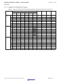
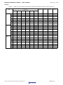
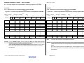
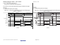
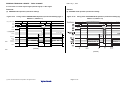
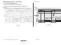
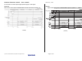
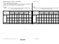
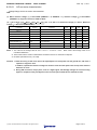
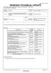
Date: July. 1, 2014 RENESAS TECHNICAL UPDATE 1753, Shimonumabe, Nakahara-ku, Kawasaki-shi, Kanagawa 211-8668 Japan Renesas Electronics Corporation Product Category Title MPU/MCU Document No. TN-RL*-A028A/E Notification of correction for Incorrect Description and Extended Specification RL78/G1A Descriptions in the Hardware User’s Manual Rev. 2.00 Changed Information Category Technical Notification Reference Document RL78/G1A User’s Manual: Hardware Rev.2.00 R01UH0305EJ0200 (Jul. 2013) Rev. 1.00 Lot No. Applicable Product RL78/G1A R5F10Exx All lots This document describes misstatements found and Extended Specification in the RL78/G1A User’s Manual: Hardware Rev.2.00 (R01UH0305EJ0200). Corrections Applicable Item 4.3 Registers Controlling Port Function 5.3.9 High-speed on-chip oscillator trimming register (HIOTRM) 12.5.7 SNOOZE mode function Timing Chart of SNOOZE Mode Operation (Figure12-70 , 12-72) 12.6.3 SNOOZE mode function 12.6.3 SNOOZE mode function Timing Chart of SNOOZE Mode Operation (Figure12-89 ,12-90 ,12-92) 16.4.3 Multiple interrupt servicing Table 16-5. Relationship Between Interrupt Requests Enabled for Multiple Interrupt Servicing During Interrupt Servicing 20.2 Configuration of Power-on-reset Circuit Figure 20-2. Timing of Generation of Internal Reset Signal by Power-on-reset Circuit and Voltage Detector (1/3) 29.6.1 A/D converter characteristics 29.7 Data Memory STOP Mode Low Supply Voltage Data Retention Characteristics 30.7 Data Memory STOP Mode Low Supply Voltage Data Retention Characteristics Applicable Page p.103 p.157 p.495 , p.497 p.522 p.524 , p.525 , p.527 Contents Incorrect descriptions revised Incorrect descriptions revised Incorrect descriptions revised attention added Incorrect descriptions revised Incorrect descriptions revised p.710 Incorrect descriptions revised p.751 p.896 p.904 p.950 Specifications extended content change content change Document Improvement The above corrections will be made for the next revision of the User’s Manual: Hardware. (c) 2014. Renesas Electronics Corporation. All rights reserved. Page 1 of 17 RENESAS TECHNICAL UPDATE TN-RL*-A028A/E Date: July. 1, 2014 Corrections in the User’s Manual: Hardware No. 1 2 3 4 5 6 7 8 9 10 Corrections and Applicable Items Document No. English R01UH0305EJ0200 4.3 Registers Controlling Port Function p.103 5.3.9 High-speed on-chip oscillator trimming p.157 register (HIOTRM) 12.5.7 SNOOZE mode function p.495 , p.497 12.6.3 SNOOZE mode function p.522 12.6.3 SNOOZE mode function p.524 , p.525 , p.527 Timing Chart of SNOOZE Mode Operation 16.4.3 Multiple interrupt servicing Table 16-5. Relationship Between Interrupt p.710 Requests Enabled for Multiple Interrupt Servicing During Interrupt Servicing 20.2 Configuration of Power-on-reset Circuit Figure 20-2. Timing of Generation of Internal p.751 Reset Signal by Power-on-reset Circuit and Voltage Detector (1/3) 29.6.1 A/D converter characteristics p.896 29.7 Data Memory STOP Mode Low Supply p.904 Voltage Data Retention Characteristics 30.7 Data Memory STOP Mode Low Supply p.950 Voltage Data Retention Characteristics Pages in this document for corrections Page 3 and Page 4 Page 5 Page 6 and 7 Page 8 Pages 9 to 11 Page 12 Page 13 Page 14 and 15 Page 16 Page 17 Incorrect: Bold with underline; Correct: Gray hatched Old: Bold with underline; New: Gray hatched Revision History RL78/G1A User’s Manual: Hardware Rev.2.00 Notification of correction for Incorrect Description and Extended Specification Document Number TN-RL*-A028A/E Date July.1.2014 (c) 2014. Renesas Electronics Corporation. All rights reserved. Description First edition issued No.1 to 10 in corrections (This notice) Page 2 of 17 RENESAS TECHNICAL UPDATE TN-RL*-A028A/E Date: July. 1, 2014 Incorrect: 1. 4.3 Registers Controlling Port Function Table 4-4. PMxx, Pxx, PUxx, PIMxx, POMxx, PMCxx registers and the bits mounted on each product (1/2) Port Port 0 Port 1 Port 2 Bit Name 64-pin 48-pin 32-pin 25-pin PMxx Pxx PUxx PIMxx POMxx PMCxx Register Register Register Register Register Register 0 PM00 P00 PU00 PIM00 1 PM01 P01 PU01 PIM01 2 PM02 P02 PU02 POM02 PMC02 3 PM03 P03 PU03 PIM03 POM03 PMC03 4 PM04 P04 PU04 PIM04 POM04 5 PM05 P05 PU05 6 PM06 P06 PU06 0 PM10 P10 PU10 PIM10 POM10 PMC00 1 PM11 P11 PU11 PIM11 POM11 PMC01 2 PM12 P12 PU12 POM12 PMC02 3 PM13 P13 PU13 POM13 PMC03 4 PM14 P14 PU14 PIM14 POM14 PMC04 5 PM15 P15 PU15 PIM15 POM15 PMC05 6 PM16 P16 PU16 PIM16 0 PM20 P20 1 PM21 P21 2 PM22 P22 3 PM23 P23 4 PM24 P24 5 PM25 P25 6 PM26 P26 7 PM27 P27 (c) 2014. Renesas Electronics Corporation. All rights reserved. Page 3 of 17 RENESAS TECHNICAL UPDATE TN-RL*-A028A/E Date: July. 1, 2014 Correct: Table 4-4. PMxx, Pxx, PUxx, PIMxx, POMxx, PMCxx registers and the bits mounted on each product (1/2) Port Port 0 Port 1 Port 2 Bit Name 64-pin 48-pin 32-pin 25-pin PMxx Pxx PUxx PIMxx POMxx PMCxx Register Register Register Register Register Register 0 PM00 P00 PU00 PIM00 1 PM01 P01 PU01 PIM01 2 PM02 P02 PU02 POM02 PMC02 3 PM03 P03 PU03 PIM03 POM03 PMC03 4 PM04 P04 PU04 PIM04 POM04 5 PM05 P05 PU05 6 PM06 P06 PU06 0 PM10 P10 PU10 PIM10 POM10 PMC10 1 PM11 P11 PU11 PIM11 POM11 PMC11 2 PM12 P12 PU12 POM12 PMC12 3 PM13 P13 PU13 POM13 PMC13 4 PM14 P14 PU14 PIM14 POM14 PMC14 5 PM15 P15 PU15 PIM15 POM15 PMC15 6 PM16 P16 PU16 PIM16 0 PM20 P20 1 PM21 P21 2 PM22 P22 3 PM23 P23 4 PM24 P24 5 PM25 P25 6 PM26 P26 7 PM27 P27 (c) 2014. Renesas Electronics Corporation. All rights reserved. Page 4 of 17 RENESAS TECHNICAL UPDATE TN-RL*-A028A/E Date: July. 1, 2014 2. 5.3.9 High-speed on-chip oscillator trimming register (HIOTRM) Incorrect: 5.3.9 Correct: High-speed on-chip oscillator trimming register (HIOTRM) (omitted) Figure 5-10. Address: 5.3.9 Format of High-Speed On-Chip Oscillator Trimming Register (HIOTRM) F00A0H After reset: undefined Note R/W High-speed on-chip oscillator trimming register (HIOTRM) (omitted) Figure 5-10. Address: Format of High-Speed On-Chip Oscillator Trimming Register (HIOTRM) F00A0H After reset: undefined Note R/W Symbol 7 6 5 4 3 2 1 0 Symbol 7 6 5 4 3 2 1 0 HIOTRM 0 0 HIOTRM5 HIOTRM4 HIOTRM3 HIOTRM2 HIOTRM1 HIOTRM0 HIOTRM 0 0 HIOTRM5 HIOTRM4 HIOTRM3 HIOTRM2 HIOTRM1 HIOTRM0 HIOTRM5 HIOTRM4 HIOTRM3 HIOTRM2 HIOTRM1 HIOTRM0 High-speed on-chip oscillator 0 0 0 0 0 0 0 0 0 0 0 0 1 0 0 0 0 0 0 0 1 0 0 0 1 0 HIOTRM4 HIOTRM3 HIOTRM2 HIOTRM1 HIOTRM0 0 0 0 0 0 1 0 0 0 0 0 1 0 0 0 0 0 1 0 1 0 0 0 0 1 1 0 0 0 0 1 0 0 1 1 1 1 0 1 1 1 1 1 1 Maximum speed The value after reset is the value adjusted at shipment. Remarks 1. The HIOTRM register can be used to adjust the high-speed on-chip oscillator clock to an accuracy within about 0.05%. High-speed on-chip oscillator 0 1 Note Minimum speed HIOTRM5 1 1 1 1 1 0 1 1 1 1 1 1 Note Minimum speed Maximum speed The value after reset is the value adjusted at shipment. Remarks 1. The HIOTRM register holds a six-bit value used to adjust the high-speed on-chip oscillator with an increment of 1 corresponding to an increase of frequency by about 2. For the usage example of the HIOTRM register, see the application note for RL78 0.05%. MCU series High-speed On-chip Oscillator (HOCO) Clock Frequency Correction 2. For the usage example of the HIOTRM register, see the application note for RL78 (R01AN0464). MCU series High-speed On-chip Oscillator (HOCO) Clock Frequency Correction (R01AN0464). (c) 2014. Renesas Electronics Corporation. All rights reserved. Page 5 of 17 RENESAS TECHNICAL UPDATE TN-RL*-A028A/E Date: July. 1, 2014 3. 12.5.7 SNOOZE mode function Timing Chart of SNOOZE Mode Operation It is correction of “Clock request signal (internal signal)” and TSF00 in this Figure. Correct: Incorrect: (1) SNOOZE mode operation (once startup) (1) SNOOZE mode operation (once startup) Figure 12-70. Timing Chart of SNOOZE Mode Operation (Once Startup) (Type 1: Figure 12-70. Timing Chart of SNOOZE Mode Operation (Once Startup) (Type 1: DAPmn = 0, CKPmn = 0) DAPmn = 0, CKPmn = 0) CPU operation status Normal operation STOP mode <4> <3> SS00 SNOOZE mode Normal operation <11> ST00 <1> <9> SE00 SWC0 SSEC0 <10> L Clock request signal (internal signal) Receive data 2 SDR00 Receive data 1 <8> Read Note SCK00 pin SI00 pin Receive data 1 Shift register 00 INTCSI00 Reception & shift operation Receive data 2 Reception & shift operation Data reception Data reception TSF00 <2> <7> <5><6> (omitted) (omitted) (c) 2014. Renesas Electronics Corporation. All rights reserved. Page 6 of 17 RENESAS TECHNICAL UPDATE TN-RL*-A028A/E Date: July. 1, 2014 It is correction of “Clock request signal (internal signal)” in this Figure. Incorrect: Correct: (2) SNOOZE mode operation (continuous startup) Figure 12-72. (2) SNOOZE mode operation (continuous startup) Timing Chart of SNOOZE Mode Operation (Continuous Startup) (Type 1: DAPmn = 0, CKPmn = 0) CPU operation status Normal operation <3> SS00 STOP mode SNOOZE mode ST00 <1> Timing Chart of SNOOZE Mode Operation (Continuous Startup) (Type 1: DAPmn = 0, CKPmn = 0) Normal operation STOP mode <4> <3> <4> Figure 12-72. SNOOZE mode <9> SE00 SWC0 SSEC0 <10> L Clock request signal (internal signal) Receive data 2 SDR00 Receive data 1 <8> ReadNote SCK00 pin <R> SI00 pin Shift register 00 INTCSI00 Receive data 1 Receive data 2 Reception & shift operation Reception & shift operation Data reception Data reception TSF00 <2> <R> <5><6> <7> <2> <5><6> (omitted) (omitted) (c) 2014. Renesas Electronics Corporation. All rights reserved. Page 7 of 17 RENESAS TECHNICAL UPDATE TN-RL*-A028A/E Date: July. 1, 2014 3. 12.6.3 Attention added of SNOOZE mode function 12.6.3 SNOOZE mode function Incorrect: Correct: 12.6.3 SNOOZE mode function The SNOOZE mode makes the UART perform reception operations upon RxDq pin input 12.6.3 SNOOZE mode function The SNOOZE mode makes the UART perform reception operations upon RxDq pin input detection while in the STOP mode. Normally the UART stops communication in the STOP detection while in the STOP mode. Normally the UART stops communication in the STOP mode. mode. However, using the SNOOZE mode enables the UART to perform reception operations without CPU operation. However, using the SNOOZE mode enables the UART to perform reception operations without CPU operation. (omitted) (omitted) Cautions 1. The SNOOZE mode can only be used when the high-speed on-chip Cautions 1. The SNOOZE mode can only be used when the high-speed on-chip oscillator clock (fIH) is selected for fCLK. oscillator clock (fIH) is selected for fCLK. (omitted) (omitted) 4. If a parity error, framing error, or overrun error occurs while the SSECm bit is set to 1, the PEFmn, FEFmn, or OVFmn flag is not set and an error interrupt (INTSREq) is not generated. Therefore, when the setting of SSECm = 1 is made, clear the PEFmn, FEFmn, or OVFmn flag before setting the SWC0 bit to 1 and read the value in bits 7 to 0 (RxDq register) of the SDRm1 register. (c) 2014. Renesas Electronics Corporation. All rights reserved. 4. If a parity error, framing error, or overrun error occurs while the SSECm bit is set to 1, the PEFmn, FEFmn, or OVFmn flag is not set and an error interrupt (INTSREq) is not generated. Therefore, when the setting of SSECm = 1 is made, clear the PEFmn, FEFmn, or OVFmn flag before setting the SWC0 bit to 1 and read the value in bits 7 to 0 (RxDq register) of the SDRm1 register. 5.The CPU shifts from the STOP mode to the SNOOZE mode on detecting the valid edge of the RxDq signal. Note, however, that transfer through the UART channel may not start and the CPU may remain in the SNOOZE mode if an input pulse on the RxDq pin is too short to be detected as a start bit. In such cases, data may not be received correctly, and this may lead to a framing error or parity error in the next UART transfer. Page 8 of 17 RENESAS TECHNICAL UPDATE TN-RL*-A028A/E Date: July. 1, 2014 3. 12.6.3 SNOOZE mode function Timing Chart of SNOOZE Mode Operation It is correction of “Clock request signal (internal signal)” in this Figure. Correct: Incorrect: Figure 12-89. Timing Chart of SNOOZE Mode Operation (EOCm1 = 0, SSECm = 0/1) Figure 12-89. Timing Chart of SNOOZE Mode Operation (EOCm1 = 0, SSECm = 0/1) (omitted) (omitted) (c) 2014. Renesas Electronics Corporation. All rights reserved. Page 9 of 17 RENESAS TECHNICAL UPDATE TN-RL*-A028A/E Date: July. 1, 2014 It is correction of “Clock request signal (internal signal)” in this Figure. Incorrect: Figure 12-90. Timing Chart of SNOOZE Mode Operation (EOCm1 = 1, SSECm = 0) Correct: Figure 12-90. Timing Chart of SNOOZE Mode Operation (EOCm1 = 1, SSECm = 0) (omitted) (omitted) (c) 2014. Renesas Electronics Corporation. All rights reserved. Page 10 of 17 RENESAS TECHNICAL UPDATE TN-RL*-A028A/E Date: July. 1, 2014 It is correction of “Clock request signal (internal signal)” in this Figure. Incorrect: Figure 12-92. Timing Chart of SNOOZE Mode Operation (Abnormal Operation <2>) Correct: Figure 12-92. Timing Chart of SNOOZE Mode Operation (EOCm1 = 1, SSECm = 1) (omitted) (c) 2014. Renesas Electronics Corporation. All rights reserved. (omitted) Page 11 of 17 RENESAS TECHNICAL UPDATE TN-RL*-A028A/E Date: July. 1, 2014 4. 16.4.3 Multiple interrupt servicing Table 16-5. Relationship Between Interrupt Requests Enabled for Multiple Interrupt Servicing During Interrupt Servicing Incorrect: Table 16-5. Correct: Relationship Between Interrupt Requests Enabled for Multiple Interrupt Table 16-5. Relationship Between Interrupt Requests Enabled for Multiple Interrupt Servicing During Interrupt Servicing Multiple Interrupt Request Servicing During Interrupt Servicing Maskable Interrupt Request Software Interrupt Request Interrupt Priority Level 0 (PR = 00) Priority Level 1 (PR = 01) Priority Level 2 (PR = 10) Priority Level 3 (PR = 11) Being Serviced IE = 1 IE = 0 IE = 1 IE = 0 IE = 1 IE = 0 IE = 1 IE = 0 ISP1 = 0 ISP0 = 0 ISP1 = 0 ISP0 = 1 ISP1 = 1 ISP0 = 0 ISP1 = 1 ISP0 = 1 Maskable interrupt Software interrupt Multiple Interrupt Request Software Interrupt Request Interrupt Priority Level 0 (PR = 00) Priority Level 1 (PR = 01) Priority Level 2 (PR = 10) Priority Level 3 (PR = 11) Being Serviced IE = 1 IE = 0 IE = 1 IE = 0 IE = 1 IE = 0 IE = 1 IE = 0 ISP1 = 0 ISP0 = 0 ISP1 = 0 ISP0 = 1 ISP1 = 1 ISP0 = 0 ISP1 = 1 ISP0 = 1 Maskable interrupt Software interrupt (omitted) (c) 2014. Renesas Electronics Corporation. All rights reserved. Maskable Interrupt Request (omitted) Page 12 of 17 RENESAS TECHNICAL UPDATE TN-RL*-A028A/E Date: July. 1, 2014 5. 20.2 Configuration of Power-on-reset Circuit Figure 20-2. Timing of Generation of Internal Reset Signal by Power-on-reset Circuit and Voltage Detector (1/3) Incorrect: Correct: Figure 20-2. Timing of Generation of Internal Reset Signal by Power-on-reset Circuit Figure 20-2. Timing of Generation of Internal Reset Signal by Power-on-reset Circuit and Voltage Detector (1/3) and Voltage Detector (1/3) (1) When the externally input reset signal on the RESET pin is used (1) When the externally input reset signal on the RESET pin is used (omitted) Notes 3. The time until normal operation starts includes the following reset (omitted) Notes 3. processing time when the external reset is released (after the first release time when the external reset is released (release from the first external reset of POR) after the RESET signal is driven high (1) as well as the voltage following release from the POR state) after the RESET signal is driven high (1) stabilization wait time after VPOR (1.51 V, typ.) is reached. as well as the voltage stabilization wait time after VPOR (1.51 V, typ.) is Reset processing time when the external reset is released is shown below. reached. After the first release of POR: Reset processing time when the external reset is released is shown below. 0.672 ms (typ.), 0.832 ms (max.) (when the LVD is in use) Release from the first external reset following release from the POR state: 0.399 ms (typ.), 0.519 ms (max.) (when the LVD is off) 4. The time until normal operation starts includes the following reset processing 0.672 ms (typ.), 0.832 ms (max.) (when the LVD is in use) Reset processing time when the external reset is released after the second release of POR is shown below. After the second release of POR: 0.531 ms (typ.), 0.675 ms (max.) (when the LVD is in use) 0.259 ms (typ.), 0.362 ms (max.) (when the LVD is off) (omitted) (c) 2014. Renesas Electronics Corporation. All rights reserved. 0.399 ms (typ.), 0.519 ms (max.) (when the LVD is off) 4. Reset times in cases of release from an external reset other than the above are listed below. Release from the reset state for external resets other than the above case: 0.531 ms (typ.), 0.675 ms (max.) (when the LVD is in use) 0.259 ms (typ.), 0.362 ms (max.) (when the LVD is off) (omitted) Page 13 of 17 RENESAS TECHNICAL UPDATE TN-RL*-A028A/E Date: July. 1, 2014 6. 29.6.1 A/D converter characteristics Voltage Range of A/D conversion was extended. Old: (1) When reference voltage (+) = AVREFP/ANI0 (ADREFP1 = 0, ADREFP0 = 1), reference voltage () = AVREFM/ANI1 (ADREFM = 1), target for conversion: ANI2 to ANI12 (TA = 40 to +85C, 2.7 V AVREFP AVDD VDD 3.6 V, VSS = 0 V, AVSS = 0 V, Reference voltage (+) = AVREFP, Reference voltage () = AVREFM = 0 V, HALT mode) Parameter Symbol Resolution Conditions MIN. TYP. MAX. Unit 12 bit 1.7 3.3 LSB RES Notes 1, 2, 3 Overall error AINL Conversion time Notes 1, 2, 3 Zero-scale error Notes 1, 2, 3 Full-scale error Integral linearity error Notes 1, 2, 3 Differential linearity error Notes 1, 2, 3 Analog input voltage 12-bit resolution s tCONV ADTYP = 0, 12-bit resolution EZS 12-bit resolution 1.3 3.2 LSB EFS 12-bit resolution 0.7 2.9 LSB ILE 12-bit resolution 1.0 1.4 LSB DLE 12-bit resolution 1.2 LSB AVREFP V VAIN 3.375 0.9 0 Notes 1. TYP. Value is the average value at AVDD = AVREFP = 3 V and TA = 25C. MAX. value is the average value 3 at normalized distribution. 2. These values are the results of characteristic evaluation and are not checked for shipment. 3. Excludes quantization error (1/2 LSB). Cautions 1. Route the wiring so that noise will not be superimposed on each power line and ground line, and insert a capacitor to suppress noise. In addition, separate the reference voltage line of AVREFP from the other power lines to keep it free from the influences of noise. 2. During A/D conversion, keep a pulse, such as a digital signal, that abruptly changes its level from being input to or output from the pins adjacent to the converter pins and P20 to P27 and P150 to P154. (c) 2014. Renesas Electronics Corporation. All rights reserved. Page 14 of 17 RENESAS TECHNICAL UPDATE TN-RL*-A028A/E Date: July. 1, 2014 New: (1) When reference voltage (+) = AVREFP/ANI0 (ADREFP1 = 0, ADREFP0 = 1), reference voltage () = AVREFM/ANI1 (ADREFM = 1), target for conversion: ANI2 to ANI12 (TA = 40 to +85C, 2.4 V AVREFP AVDD VDD 3.6 V, VSS = 0 V, AVSS = 0 V, Reference voltage (+) = AVREFP, Reference voltage () = AVREFM = 0 V, HALT mode) Parameter Symbol Resolution Conditions MIN. TYP. MAX. 12 bit 1.7 3.3 LSB RES Notes 1, 2, 3 Overall error Conversion time Notes 1, 2, 3 Zero-scale error Notes 1, 2, 3 Full-scale error Integral linearity error Notes 1, 2, 3 Differential linearity error Notes 1, 2, 3 Analog input voltage Unit AINL 12-bit resolution tCONV ADTYP = 0, 12-bit resolution EZS 12-bit resolution 1.3 3.2 LSB s 3.375 EFS 12-bit resolution 0.7 2.9 LSB ILE 12-bit resolution 1.0 1.4 LSB DLE 12-bit resolution 0.9 1.2 LSB AVREFP V VAIN 0 Notes 1. TYP. Value is the average value at AVDD = AVREFP = 3 V and TA = 25C. MAX. value is the average value 3 at normalized distribution. 2. These values are the results of characteristic evaluation and are not checked for shipment. 3. Excludes quantization error (1/2 LSB). Cautions 1. Route the wiring so that noise will not be superimposed on each power line and ground line, and insert a capacitor to suppress noise. In addition, separate the reference voltage line of AVREFP from the other power lines to keep it free from the influences of noise. 2. During A/D conversion, keep a pulse, such as a digital signal, that abruptly changes its level from being input to or output from the pins adjacent to the converter pins and P20 to P27 and P150 to P154. (c) 2014. Renesas Electronics Corporation. All rights reserved. Page 15 of 17 RENESAS TECHNICAL UPDATE TN-RL*-A028A/E Date: July. 1, 2014 7. 29.7 Data Memory STOP Mode Low Supply Voltage Data Retention Characteristics Old: 29.7 Data Memory STOP Mode Low Supply Voltage Data Retention Characteristics (TA = 40 to +85C, VSS = 0 V) Parameter Data retention supply New: 29.7 RAM Data Retention Characteristics (TA = 40 to +85C, VSS = 0 V) Parameter Symbol Conditions MIN. Note 1.46 VDDDR TYP. MAX. Unit 3.6 V voltage Note The value depends on the POR detection voltage. When the voltage drops, the data is retained before a POR reset is effected, but data is not retained when a Data retention supply 1.46 Note TYP. MAX. Unit 3.6 V retained until the voltage reaches the level that triggers a POR reset but not once it reaches the level at which a POR reset is generated. Operation mode VDDDR STOP instruction execution Standby release signal (interrupt request) (c) 2014. Renesas Electronics Corporation. All rights reserved. VDDDR MIN. Note This depends on the POR detection voltage. For a falling voltage, data in RAM are Data retention mode VDD Conditions voltage POR reset is effected. STOP mode Symbol Page 16 of 17 RENESAS TECHNICAL UPDATE TN-RL*-A028A/E Date: July. 1, 2014 8. 30.7 Data Memory STOP Mode Low Supply Voltage Data Retention Characteristics Old: New: 30.7 Data Memory STOP Mode Low Supply Voltage Data Retention Characteristics 30.7 RAM Data Retention Characteristics (TA = 40 to +105C, VSS = 0 V) Parameter Data retention supply (TA = 40 to +105C, VSS = 0 V) Symbol Conditions MIN. Note 1.44 VDDDR TYP. MAX. Unit 3.6 V voltage Parameter Data retention supply Symbol Conditions VDDDR MIN. Note 1.44 TYP. MAX. Unit 3.6 V voltage Note The value depends on the POR detection voltage. When the voltage drops, the data is retained before a POR reset is effected, but data is not retained when a POR reset is effected. STOP mode Note This depends on the POR detection voltage. For a falling voltage, data in RAM are retained until the voltage reaches the level that triggers a POR reset but not once it reaches the level at which a POR reset is generated. Operation mode Data hold mode VDD VDDDR STOP instruction execution Standby release signal (inerrupt request) (c) 2014. Renesas Electronics Corporation. All rights reserved. Page 17 of 17