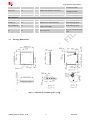
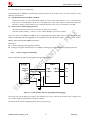
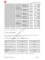
1
SIM968_Hardware Design_V1.00
Smart Machine Smart Decision
Document Title
SIM968 Hardware Design
Version
1.00
Date
2013-02-25
Status
Release
Document Control ID
SIM968_Hardware Design_V1.00
General Notes
SIMCom offers this information as a service to its customers, to support application and engineering efforts that
use the products designed by SIMCom. The information provided is based upon requirements specifically
provided to SIMCom by the customers. SIMCom has not undertaken any independent search for additional
relevant information, including any information that may be in the customer’s possession. Furthermore, system
validation of this product designed by SIMCom within a larger electronic system remains the responsibility of the
customer or the customer’s system integrator. All specifications supplied herein are subject to change.
Copyright
This document contains proprietary technical information which is the property of SIMCom Limited, copying of
this document and giving it to others and the using or communication of the contents thereof, are forbidden
without express authority. Offenders are liable to the payment of damages. All rights reserved in the event of grant
of a patent or the registration of a utility model or design. All specification supplied herein are subject to change
without notice at any time.
Copyright © Shanghai SIMCom Wireless Solutions Ltd. 2013
SIM968_Hardware Design_V1.00
2
2013.02.25
Smart Machine Smart Decision
Contents
Contents.................................................................................................................................................................... 3
Version History ........................................................................................................................................................ 7
1
Introduction....................................................................................................................................................... 8
2
SIM968 Overview ............................................................................................................................................. 8
2.1
SIM968 Key Features............................................................................................................................... 9
2.2
Operating Modes .....................................................................................................................................11
2.3
SIM968 Functional Diagram .................................................................................................................. 12
3
Package Information ...................................................................................................................................... 13
3.1
Pin out Diagram...................................................................................................................................... 13
3.2
Pin Description ....................................................................................................................................... 13
3.3
Package Dimensions............................................................................................................................... 16
4
GSM Application Interface ............................................................................................................................ 18
4.1
GSM Power Supply ................................................................................................................................ 18
4.1.1 Minimizing Voltage Drop of VBAT ................................................................................................... 19
4.1.2 Monitoring Power Supply ................................................................................................................... 19
4.2
Power on/down Scenarios ...................................................................................................................... 19
4.2.1 Power on SIM968 ............................................................................................................................... 19
4.2.2 Power down SIM968........................................................................................................................... 21
4.2.3 Restart SIM968 by PWRKEY Pin ...................................................................................................... 22
4.3
Power Saving Mode................................................................................................................................ 23
4.3.1 Minimum Functionality Mode ............................................................................................................ 23
4.3.2 Sleep Mode 1 (AT+CSCLK=1) .......................................................................................................... 23
4.3.3 Wake Up SIM968 from Sleep Mode 1 (AT+CSCLK=1) ................................................................... 23
4.3.4 Sleep Mode 2 (AT+CSCLK=2) .......................................................................................................... 24
4.3.5 Wake Up SIM968 from Sleep Mode 2 (AT+CSCLK=2) ................................................................... 24
4.4
Charging Interface .................................................................................................................................. 24
4.4.1 Battery Pack Characteristics................................................................................................................ 25
4.4.2 Recommended Battery Pack ............................................................................................................... 25
4.4.3 Implemented Charging Technique ...................................................................................................... 25
4.4.4 Operating Modes during Charging...................................................................................................... 26
4.4.5 Charger Requirements......................................................................................................................... 27
4.5
RTC Backup ........................................................................................................................................... 27
4.6
Serial Interfaces ...................................................................................................................................... 29
4.6.1 Function of Serial Port and Debug Port .............................................................................................. 29
4.6.2 Software Upgrade and Debug ............................................................................................................. 30
4.7
Audio Interfaces ..................................................................................................................................... 31
4.7.1 Speaker Interface Configuration ......................................................................................................... 31
4.7.2 Microphone Interfaces Configuration ................................................................................................. 32
4.7.3 Earphone Interface Configuration ....................................................................................................... 32
4.7.4 Audio Electronic Characteristics......................................................................................................... 32
4.8
SIM Card Interface ................................................................................................................................. 33
4.8.1 SIM Card Application ......................................................................................................................... 33
SIM968_Hardware Design_V1.00
3
2013.02.25
Smart Machine Smart Decision
4.8.2
4.9
4.10
4.11
4.12
4.13
4.14
4.15
4.16
4.17
4.18
Design Considerations for SIM Card Holder ...................................................................................... 34
LCD Display/SPI Interface..................................................................................................................... 36
Keypad Interface .................................................................................................................................... 36
ADC........................................................................................................................................................ 37
RI Behaviors........................................................................................................................................... 37
Network Status Indication ...................................................................................................................... 38
General Purpose Input/Output (GPIO) ................................................................................................... 39
External Reset......................................................................................................................................... 39
PWM ...................................................................................................................................................... 40
I2C Bus.................................................................................................................................................... 40
GSM Antenna Interface.......................................................................................................................... 40
5
GNSS Application Interface........................................................................................................................... 42
5.1
Power Management ................................................................................................................................ 42
5.1.1 GNSS Power Input.............................................................................................................................. 42
5.1.2 Starting GNSS Engine......................................................................................................................... 42
5.1.3 Verification of GNSS Engine Start...................................................................................................... 42
5.1.4 Power Saving Modes........................................................................................................................... 42
5.1.5 Operating Mode .................................................................................................................................. 42
5.1.6 GPS_VANT_OUT and GPS_VANT_IN............................................................................................ 43
5.2
UART Interface ...................................................................................................................................... 44
5.3
1PPS Output ........................................................................................................................................... 44
5.4
A-GPS .................................................................................................................................................... 44
5.4.1 EPO ..................................................................................................................................................... 44
5.4.2 EASY MODE...................................................................................................................................... 45
5.4.3 SBAS and RTCM................................................................................................................................ 45
5.5
GNSS Antenna Interface ........................................................................................................................ 45
5.5.1 GNSS Antenna Interface..................................................................................................................... 45
5.5.2 GNSS Antenna Choice Consideration ................................................................................................ 46
5.5.3 Active antenna supervisor ................................................................................................................... 47
6
Electrical, Reliability and Radio Characteristics......................................................................................... 49
6.1
Absolute Maximum Ratings................................................................................................................... 49
6.2
Recommended Operating Conditions..................................................................................................... 49
6.3
Digital Interface Characteristics ............................................................................................................. 49
6.4
SIM Card Interface Characteristics ........................................................................................................ 50
6.5
VDD_EXT Characteristics ..................................................................................................................... 50
6.6
SIM_VDD Characteristics...................................................................................................................... 51
6.7
VRTC Characteristics ............................................................................................................................. 51
6.8
Current Consumption (VBAT = 3.8V) ................................................................................................... 51
6.9
Electro-Static Discharge ......................................................................................................................... 52
6.10
Radio Characteristics.............................................................................................................................. 53
6.10.1
Module RF Output Power................................................................................................................ 53
6.10.2
Module RF Receive Sensitivity ....................................................................................................... 54
6.10.3
Module Operating Frequencies........................................................................................................ 54
6.11
Module label information ....................................................................................................................... 55
Appendix ................................................................................................................................................................ 56
A. Related Documents.......................................................................................................................................... 56
B. Terms and Abbreviations ................................................................................................................................. 57
SIM968_Hardware Design_V1.00
4
2013.02.25
Smart Machine Smart Decision
C. Safety Caution ................................................................................................................................................. 58
Table Index
TABLE 1: SIM968 GSM/GPRS ENGINE KEY FEATURES ........................................................................................... 9
TABLE 2: GNSS ENGINE PERFORMANCE ................................................................................................................ 10
TABLE 3: CODING SCHEMES AND MAXIMUM NET DATA RATES OVER AIR INTERFACE ............................ 11
TABLE 4: OVERVIEW OF OPERATING MODES........................................................................................................ 11
TABLE 5: PIN DESCRIPTION ....................................................................................................................................... 13
TABLE 6: THE CURRENT CONSUMPTION OF MINIMUM FUNCTIONALITY MODE ........................................ 23
TABLE 7: SPECIFICATION OF RECOMMENDED BATTERY PACK........................................................................ 25
TABLE 8: CHARGE OPERATING MODES .................................................................................................................. 26
TABLE 9: AT COMMAND USUALLY USED IN CHARGE-ONLY MODE ................................................................ 27
TABLE 10: MICROPHONE INPUT CHARACTERISTICS........................................................................................... 32
TABLE 11: AUDIO OUTPUT CHARACTERISTICS .................................................................................................... 33
TABLE 12: PIN DESCRIPTION (AMPHENOL SIM CARD HOLDER)....................................................................... 35
TABLE 13: PIN DESCRIPTION (MOLEX SIM CARD HOLDER) .............................................................................. 35
TABLE 14: PIN DEFINITION OF THE KEYPAD INTERFACE................................................................................... 36
TABLE 15: ADC SPECIFICATION ................................................................................................................................ 37
TABLE 16: RI BEHAVIORS ........................................................................................................................................... 37
TABLE 17: STATUS OF THE NETLIGHT PIN.............................................................................................................. 38
TABLE 18: PIN DEFINITION OF THE GPIO INTERFACE ......................................................................................... 39
TABLE 19: POWER SUPPLY AND CLOCK STATE ACCORDING TO OPERATION MODE................................... 42
TABLE 20: ABSOLUTE MAXIMUM RATINGS OF GSM ........................................................................................... 49
TABLE 21: ABSOLUTE MAXIMUM RATINGS OF GNSS.......................................................................................... 49
TABLE 22: RECOMMENDED OPERATING CONDITIONS ....................................................................................... 49
TABLE 23: DIGITAL INTERFACE CHARACTERISTICS OF GSM............................................................................ 49
TABLE 24: DIGITAL INTERFACE CHARACTERISTICS OF GNSS .......................................................................... 50
TABLE 25: SIM CARD INTERFACE CHARACTERISTICS........................................................................................ 50
TABLE 26: VDD_EXT CHARACTERISTICS ............................................................................................................... 50
TABLE 27: SIM_VDD CHARACTERISTICS................................................................................................................ 51
TABLE 28: VRTC CHARACTERISTICS ....................................................................................................................... 51
TABLE 29: GSM CURRENT CONSUMPTION*............................................................................................................ 51
TABLE 30: THE ESD CHARACTERISTICS (TEMPERATURE: 25℃, HUMIDITY: 45 %) ....................................... 52
TABLE 31: SIM968 GSM 900 AND GSM 850 CONDUCTED RF OUTPUT POWER ................................................ 53
TABLE 32: SIM968 DCS 1800 AND PCS 1900 CONDUCTED RF OUTPUT POWER............................................... 53
TABLE 33: SIM968 CONDUCTED RF RECEIVE SENSITIVITY ............................................................................... 54
TABLE 34: SIM968 OPERATING FREQUENCIES....................................................................................................... 54
TABLE 35: ILLUSTRATION OF MODULE LABEL .................................................................................................... 55
TABLE 36: RELATED DOCUMENTS ........................................................................................................................... 56
TABLE 37: TERMS AND ABBREVIATIONS................................................................................................................ 57
TABLE 38: SAFETY CAUTION..................................................................................................................................... 58
SIM968_Hardware Design_V1.00
5
2013.02.25
Smart Machine Smart Decision
Figure Index
FIGURE 1: SIM968 FUNCTIONAL DIAGRAM ........................................................................................................... 12
FIGURE 2: SIM968 PIN OUT DIAGRAM (TOP VIEW) ............................................................................................... 13
FIGURE 3: DIMENSIONS OF SIM968(UNIT: MM)................................................................................................ 16
FIGURE 4: RECOMMENDED PCB FOOTPRINT OUTLINE(UNIT: MM)............................................................ 17
FIGURE 5: REFERENCE CIRCUIT OF THE LDO POWER SUPPLY ......................................................................... 18
FIGURE 6: REFERENCE CIRCUIT OF THE DC-DC POWER SUPPLY..................................................................... 18
FIGURE 7: VBAT VOLTAGE DROP DURING TRANSMIT BURST........................................................................... 19
FIGURE 8: THE MINIMAL VBAT VOLTAGE REQUIREMENT AT VBAT DROP .................................................... 19
FIGURE 9: POWERED ON/DOWN MODULE USING TRANSISTOR....................................................................... 19
FIGURE 10: POWERED ON/DOWN MODULE USING BUTTON ............................................................................. 20
FIGURE 11: TIMING OF POWER ON MODULE......................................................................................................... 20
FIGURE 12: TIMING OF POWER DOWN SIM968 BY PWRKEY .............................................................................. 21
FIGURE 13: TIMING OF RESTART SIM968 ................................................................................................................ 22
FIGURE 14: SIM968 WITH BATTERY CHARGER AND PACK CONNECTION....................................................... 24
FIGURE 15: RTC SUPPLY FROM CAPACITOR........................................................................................................... 28
FIGURE 16: RTC SUPPLY FROM NON-CHARGEABLE BATTERY ......................................................................... 28
FIGURE 17: RTC SUPPLY FROM RECHARGEABLE BATTERY .............................................................................. 28
FIGURE 18: SEIKO XH414H-IV01E CHARGE-DISCHARGE CHARACTERISTIC ................................................. 28
FIGURE 19: CONNECTION OF THE SERIAL INTERFACES..................................................................................... 29
FIGURE 20: CONNECTION OF RXD AND TXD ONLY ............................................................................................. 29
FIGURE 21: CONNECTION FOR SOFTWARE UPGRADING AND DEBUGGING.................................................. 30
FIGURE 22: SPEAKER REFERENCE CIRCUIT .......................................................................................................... 31
FIGURE 23: SPEAKER WITH AMPLIFIER REFERENCE CIRCUIT ......................................................................... 31
FIGURE 24 : MICROPHONE REFERENCE CIRCUIT................................................................................................. 32
FIGURE 25: EARPHONE REFERENCE CIRCUIT....................................................................................................... 32
FIGURE 26: REFERENCE CIRCUIT OF THE 8-PIN SIM CARD HOLDER............................................................... 33
FIGURE 27: REFERENCE CIRCUIT OF THE 6-PIN SIM CARD HOLDER............................................................... 34
FIGURE 28: AMPHENOL C707 10M006 5122 SIM CARD HOLDER......................................................................... 34
FIGURE 29: MOLEX 91228 SIM CARD HOLDER ...................................................................................................... 35
FIGURE 30: REFERENCE CIRCUIT OF THE KEYPAD INTERFACE ....................................................................... 36
FIGURE 31: RI BEHAVIOUR OF VOICE CALLING AS A RECEIVER...................................................................... 37
FIGURE 32: RI BEHAVIOUR OF DATA CALLING AS A RECEIVER........................................................................ 38
FIGURE 33: RI BEHAVIOUR OF URC OR RECEIVE SMS ........................................................................................ 38
FIGURE 34: RI BEHAVIOUR AS A CALLER ............................................................................................................... 38
FIGURE 35: REFERENCE CIRCUIT OF NETLIGHT .................................................................................................. 39
FIGURE 36: RESET TIMING ......................................................................................................................................... 39
FIGURE 37: RESET REFERENCE DESIGN CIRCUIT ................................................................................................ 40
FIGURE 38: THE RF INTERFACE OF MODULE......................................................................................................... 41
FIGURE 39: GSM ANTENNA MATCHING CIRCUIT ................................................................................................. 41
FIGURE 40: INTERNAL SUPPLY ANTENNA BIAS VOLTAGE ................................................................................. 44
FIGURE 41: EXTERNAL SUPPLY ANTENNA BIAS VOLTAGE................................................................................ 44
FIGURE 42: GNSS ANTENNA MATCHING CIRCUIT ................................................................................................ 46
FIGURE 43: OPEN CIRCUIR DETECTION-A.............................................................................................................. 48
FIGURE 44: OPEN CIRCUIR DETECTION-B .............................................................................................................. 48
FIGURE 45: MODULE LABEL INFORMATION.......................................................................................................... 55
SIM968_Hardware Design_V1.00
6
2013.02.25
Smart Machine Smart Decision
Version History
Date
Version
Description of change
Author
2013-02-25
1.00
Origin
Shengwu.sun,
Xiaohan.jin
SIM968_Hardware Design_V1.00
7
2013.02.25
Smart Machine Smart Decision
1
Introduction
This document describes SIM968 hardware interface in great detail.
This document can help user to quickly understand SIM968 interface specifications, electrical and mechanical
details. With the help of this document and other SIM968 application notes, user guide, users can use SIM968 to
design various applications quickly.
2
SIM968 Overview
Designed for global market, SIM968 is integrated with a high performance GSM/GPRS engine and a GNSS
engine. They are independent with each other. The GSM/GPRS engine is a quad-band, GSM/GPRS module that
works on frequencies GSM 850MHz, EGSM 900MHz, DCS 1800MHz and PCS 1900MHz. SIM968 features
GPRS multi-slot class 10/ class 8 (optional) and supports the GPRS coding schemes CS-1, CS-2, CS-3 and CS-4.
The GNSS solution offers best- in-class acquisition and tracing sensitivity, Time-To-First-Fix (TTFF) and
accuracy.
With built-in LNA, SIM968 doesn’t need external LNA. SIM968 can track as low as -167dBm signal even
without network assistance. The SIM968 has excellent low power consumption characteristic (acquisition 34mA,
tracking 37mA). SIM968 supports various location and navigation applications, including autonomous GPS,
GLONASS, GALILEO,QZSS, SBAS (WAAS, EGNOS, GAGAN, MSAS), DGPS (RTCM), and A-GPS.
With a tiny configuration of 30*30*3mm, SIM968 can meet almost all the space requirements in user applications,
such as M2M, smart phone, PDA, tracker and other mobile devices.
SIM968 has 80 SMT pads, and provides all hardware interfaces between the module and customers’ boards.
z Serial port and debug port can help user develop their applications easily.
z GNSS Serial port.
z Audio channels include two inputs and two outputs. These can be easily configured by AT command.
z Charging interface.
z Programmable general purpose input and output.
z The keypad and SPI display interfaces will bring users convenience to develop customized applications.
z RF pad interface.
z Output navigation solution in NMEA protocol format.
z Supports FCC E911 compliance and A-GPS
z 33tracking/99 acquisition-channel GNSS receiver
z Accuracy <2.5m CEP
z RoHS compliant
z Active antenna supervisor
SIM968 is designed with power saving technique so that the current consumption is as low as 1.2mA in sleep
mode (GNSS engine is powered down).
SIM968 integrates TCP/IP protocol and extended TCP/IP AT commands which are very useful for data transfer
applications. For details about TCP/IP applications, please refer to document [2].
SIM968_Hardware Design_V1.00
8
2013.02.25
Smart Machine Smart Decision
2.1
SIM968 Key Features
Table 1: SIM968 GSM/GPRS engine key features
Feature
Implementation
Power supply
3.2V ~ 4.8V
Power saving
Typical power consumption in sleep mode is 1.2mA ( BS-PA-MFRMS=9, GNSS
engine is powered down )
Charging
Supports charging control for Li-Ion battery
z
z
SIM968 Quad-band: GSM 850, EGSM 900, DCS 1800, PCS 1900. SIM968
can search the 4 frequency bands automatically. The frequency bands also
can be set by AT command “AT+CBAND”. For details, please refer to
document [1].
Compliant to GSM Phase 2/2+
Transmitting power
z
z
Class 4 (2W) at GSM 850 and EGSM 900
Class 1 (1W) at DCS 1800 and PCS 1900
GPRS connectivity
z
z
GPRS multi-slot class 10(default)
GPRS multi-slot class 8 (option)
Temperature range
z
z
z
Normal operation: -30℃ ~ +80℃
Restricted operation: -40℃~ -30℃ and +80℃ ~ +85℃
Storage temperature -45℃~ +90℃
Data GPRS
z
z
z
z
z
GPRS data downlink transfer: max. 85.6 kbps
GPRS data uplink transfer: max. 42.8 kbps
Coding scheme: CS-1, CS-2, CS-3 and CS-4
Integrate the TCP/IP protocol.
Support Packet Broadcast Control Channel (PBCCH)
CSD
z
Support CSD transmission
USSD
z
Unstructured Supplementary Services Data (USSD) support
SMS
z
z
MT, MO, CB, Text and PDU mode
SMS storage: SIM card
FAX
Group 3 Class 1
SIM interface
Support SIM card: 1.8V, 3V
External antenna
Antenna pad
Audio features
Speech codec modes:
z Half Rate (ETS 06.20)
z Full Rate (ETS 06.10)
z Enhanced Full Rate (ETS 06.50 / 06.60 / 06.80)
z Adaptive multi rate (AMR)
z Echo Cancellation
z Noise Suppression
Frequency bands
Serial port and
debug port
SIM968_Hardware Design_V1.00
z
Serial port:
Full modem interface with status and control lines, unbalanced,
asynchronous.
9
2013.02.25
Smart Machine Smart Decision
z
z
z
z
z
z
z
*
1200bps to 115200bps.
Can be used for AT commands or data stream.
Support RTS/CTS hardware handshake and software ON/OFF flow control.
Multiplex ability according to GSM 07.10 Multiplexer Protocol.
Autobauding supports baud rate from 1200 bps to 57600bps.
Debug port:
Null modem interface DBG_TXD and DBG_RXD.
Can be used for debugging and upgrading firmware.
Phonebook management
Support phonebook types: SM, FD, LD, RC, ON, MC.
SIM application toolkit
GSM 11.14 Release 99
Real time clock
Support RTC
Physical characteristics
Size: 30*30*3mm
Weight: 5.3g
Firmware upgrade
Firmware upgradeable by debug port.
SIM968 does work at this temperature, but some radio frequency characteristics may deviate from the GSM specification.
Table 2: GNSS engine Performance
Parameter
Performance
Description
Min
Type
Max
Unit
Horizontal Position
Accuracy(1)
Autonomous
<2.5
m
Velocity
Accuracy(2)
Without Aid
0.1
m/s
DGPS
0.05
m/s
Acceleration
Accuracy
Without Aid
0.1
m/s2
DGPS
0.05
m/s2
10
nS
Timing Accuracy
Dynamic
Performance
Time To First Fix(3)
A-GPS TTFF(EPO
in flash mode)
Sensitivity
Receiver
Maximum Altitude
18000
m
Maximum Velocity
515
m/s
Maximum
Acceleration
4
G
Hot start
<1
s
Warm start
26
s
Cold start
28
s
Hot start
0.7
s
Warm start
1.5
s
Cold start
12.5
s
Autonomous
acquisition(cold start)
-148
dBm
Re-acquisition
-160
dBm
Tracking
-167
dBm
Channels
132
Update rate
1
10
Hz
Tracking L1, CA
SIM968_Hardware Design_V1.00
10
2013.02.25
Smart Machine Smart Decision
Code
Protocol support
NMEA,PMTK
Power
consumption(4)
Acquisition
34
mA
Continuous tracking
37
mA
Sleep current
440
uA
Backup current
14
uA
(1) 50% 24hr static, -130dBm
(2) 50% at 30m/s
(3) –130 dBm, GPS&GLONASS mode
(4) Single Power supply 3.3V under GPS+GLONASS signal
Table 3: Coding schemes and maximum net data rates over air interface
Coding scheme
1 timeslot
2 timeslot
4 timeslot
CS-1
9.05kbps
18.1kbps
36.2kbps
CS-2
13.4kbps
26.8kbps
53.6kbps
CS-3
15.6kbps
31.2kbps
62.4kbps
CS-4
21.4kbps
42.8kbps
85.6kbps
2.2
Operating Modes
The table below summarizes the various operating modes of SIM968.
Table 4: Overview of operating modes
Mode
Normal
operation
Function
GSM/GPRS
SLEEP
Module will automatically go into sleep mode if the conditions of sleep
mode are enabling and there is no on air and no hardware interrupt (such as
GPIO interrupt or data on serial port).
In this case, the current consumption of module will reduce to the minimal
level.
In sleep mode, the module can still receive paging message and SMS.
GSM
IDLE
Software is active. Module registered to the GSM network, and the module
is ready to communicate.
GSM
TALK
Connection between two subscribers is in progress. In this case, the power
consumption depends on network settings such as DTX off/on,
FR/EFR/HR, hopping sequences, antenna.
GPRS
STANDBY
Module is ready for GPRS data transfer, but no data is currently sent or
received. In this case, power consumption depends on network settings and
GPRS configuration.
GPRS
DATA
There is GPRS data transfer (PPP or TCP or UDP) in progress. In this case,
power consumption is related with network settings (e.g. power control
level); uplink/downlink data rates and GPRS configuration (e.g. used
multi-slot settings).
SIM968_Hardware Design_V1.00
11
2013.02.25
Smart Machine Smart Decision
Power down
Normal power down by sending the AT command “AT+CPOWD=1” or using the PWRKEY.
The power management unit shuts down the power supply for the baseband part of the
module, and only the power supply for the RTC is remained. Software is not active. The
serial port is not accessible. Power supply (connected to VBAT) remains applied.
Minimum
functionality
mode
AT command “AT+CFUN” can be used to set the module to a minimum functionality mode
without removing the power supply. In this mode, the RF part of the module will not work or
the SIM card will not be accessible, or both RF part and SIM card will be closed, and the
serial port is still accessible. The power consumption in this mode is lower than normal
mode.
Charge-only
mode
The module will enter Charge-only mode automatically when a charger and battery are
connected to a switched-off SIM968. In this mode, the module does not search for network
and has limited access to available AT commands available. The module can also enter
Charge-only mode from Charge mode during normal operation by normally powered down
the module.
Charge
mode
during normal
operation
The module will automatically go to this mode when a charger is connected to a Normal
operation mode module when battery voltage is not lower than 3.2V. Normal operation mode
includes: SLEEP, IDLE, TALK, GPRS IDLE and GPRS DATA.
2.3
SIM968 Functional Diagram
The following figure shows a functional diagram of SIM968:
z The GSM baseband engine
z The GNSS engine
z Flash
z The GSM radio frequency part
z The antenna interface
z The other interfaces
RTC
Power management unit
Power
supply
Power
supply
GNSS
engine
Radio
Frequency
Digital Interface
Analog Interface
Analog base
band
Digital base
band
SIM
UART
Keypad/
GPIOs
PWMs
Audio
I2C
LCD/SPI
ADC
GNSS
UART
FLASH
Figure 1: SIM968 functional diagram
SIM968_Hardware Design_V1.00
12
2013.02.25
Smart Machine Smart Decision
3
3.1
Package Information
Pin out Diagram
Figure 2: SIM968 pin out diagram (Top view)
3.2
Pin Description
Table 5: Pin description
SIM968_Hardware Design_V1.00
13
2013.02.25
Smart Machine Smart Decision
Pin name
Pin number
I/O
Description
Comment
62, 63
I
GSM power supply
3.2V ~ 4.8V
Power supply
VBAT
VRTC
42
I/O
Power supply for GSM RTC
It is recommended to
connect with a battery or
a capacitor (e.g. 4.7uF).
VDD_EXT
44
O
2.8V output power supply
If it is unused, keep open.
GPS_VCC
12
I
GNSS Power supply
2.8V~4.3V
V_BACKUP
13
I
Power supply for GNSS RTC
It is recommended to
connect with a battery or
LDO
GPS_VANT_OUT
75
O
2.8V output for GNSS active antenna
If it is unused, keep open.
GPS_VANT_IN
76
I
GNSS active antenna power supply
If it is unused, keep open.
GND
1, 2, 5, 10, 14, 37,
40, 41, 43, 57, 58,
60, 61, 64, 65, 77,
78, 80
Ground
Charge interface
VCHG
74
I
Charger input
TEMP_BAT
73
I
Battery temperature sensor
I
PWRKEY should be pulled low at
least 1 second and then released to
power on/down the module.
I
Differential audio input
O
Differential audio output
I
Differential audio input
O
Differential audio output
Power on/down
PWRKEY
3
Pulled up internally.
Audio interfaces
MIC1P
23
MIC1N
24
SPK1P
22
SPK1N
21
MIC2P
27
MIC2N
28
SPK2N
25
SPK2P
26
If these pins are unused,
keep open.
Status
STATUS
52
O
Power on status
NETLIGHT
51
O
Network status
1PPS
11
O
Time Mark outputs timing pulse
related to receiver time
DISP _CLK
6
O
Display interface
DISP_DATA
7
I/O
If these pins are unused,
keep open.
If unused, keep open.
LCD interface
SIM968_Hardware Design_V1.00
14
If these pins are unused,
keep open.
2013.02.25
Smart Machine Smart Decision
DISP _D/C
8
O
DISP _CS
9
O
56
O
I2C interface
I2C_SDA
I2C_SCL
55
I/O
I2C serial bus data
If these pins are unused,
keep open.
2
I C serial bus clock
Keypad interface / GPIOs
GPIO1/KBR0
31
GPIO1/keypad row 0
GPIO2/KBR1
32
GPIO2/keypad row 1
GPIO3/KBR2
33
GPIO3/keypad row 2
I/O
GPIO4/KBC0/
SIM_PRESENCE
GPIO4/keypad column 0/ SIM card
detection
34
GPIO5/KBC1
35
GPIO5/keypad column 1
GPIO6/KBC2
36
GPIO6/keypad column 3
If these pins are unused,
keep open.
GSM Serial port/ Debug interface
RXD
68
I
Receive data
TXD
71
O
Transmit data
RTS
66
O
Request to send
CTS
67
I
Clear to send
DCD
70
O
Data carrier detect
RI
69
O
Ring indicator
DTR
72
I
Data terminal ready
DBG_TXD
38
O
DBG_RXD
39
I
For debugging
firmware
GPS_TXD
15
O
GPS_RXD
16
I
GPS_TXD1
29
O
GPS_RXD1
30
I
SIM_VDD
20
O
Voltage supply for SIM card. Support
1.8V or 3V SIM card
SIM_DATA
17
I/O
SIM data input/output
SIM_CLK
19
O
SIM clock
SIM_RST
18
O
SIM reset
47
I
Input voltage range: 0V ~ 2.8V
If only TXD and RXD
are used, it is suggested
to pull down DTR, and
others pins can be kept
open.
and
upgrading
If these pins are unused,
keep open.
GNSS Serial port
For GNSS NMEA information output
If these pins are unused,
keep open.
Serial communication for RTCM
If these pins are unused,
keep open.
SIM interface
All signals of SIM
interface
should
be
protected against ESD
with a TVS diode array.
ADC
ADC
If it is unused, keep open.
Pulse width modulation( PWM )
PWM1
48
O
PWM
PWM2
49
O
PWM
PWM3
50
O
PWM
I/O
GSM radio antenna connection
If these pins are unused,
keep open.
GSM/GNSS RF interface
GSM_ANT
59
SIM968_Hardware Design_V1.00
15
Impendence
must
2013.02.25
be
Smart Machine Smart Decision
controlled to 50Ω.
GPS_ANT
79
I
GNSS radio antenna connection
Impendence must
controlled to 50Ω.
be
RF_SYNS
53
O
RF synchronization
If unused, keep open
RESET
4
I
GSM Reset input, active low
If unused, keep open.
AADET_N
46
I
GNSS Active Antenna Detect
If unused, keep open.
GPS_WAKEUP
54
I
GNSS engine wake up from Backup
mode, active High.
If unused, keep open.
NC
45
Not Connected
This pin should be kept
open.
Other interface
3.3
Package Dimensions
Figure 3: Dimensions of SIM968(Unit: mm)
SIM968_Hardware Design_V1.00
16
2013.02.25
Smart Machine Smart Decision
Figure 4: Recommended PCB footprint outline(Unit: mm)
SIM968_Hardware Design_V1.00
17
2013.02.25
Smart Machine Smart Decision
4
4.1
GSM Application Interface
GSM Power Supply
GND
The GSM power supply range of SIM968 is from 3.2V to 4.8V. The transmitting burst will cause voltage drop
and the power supply must be able to provide sufficient current up to 2A. For the VBAT input, a bypass capacitor
(low ESR) such as a 100 µF is strongly recommended; this capacitor should be placed as close as possible to
SIM968 VBAT pins. The following figure is the reference design of +5V input power supply. The designed output
for the power supply is 4.1V, thus a linear regulator can be used.
Figure 5: Reference circuit of the LDO power supply
If there is a high drop-out between the input and the desired output (VBAT), a DC-DC power supply will be
preferable because of its better efficiency especially with the 2A peak current in burst mode of the module. The
following figure is the reference circuit.
Figure 6: Reference circuit of the DC-DC power supply
The single 3.7V Li-ion cell battery can be connected to SIM968 VBAT pins directly. But the Ni-Cd or Ni-MH
battery must be used carefully, since their maximum voltage can rise over the absolute maximum voltage of the
module and damage it.
When battery is used, the total impedance between battery and VBAT pins should be less than 150mΩ.
The following figure shows the VBAT voltage drop at the maximum power transmit phase, and the test condition
is as following:
VBAT=4.0V,
A VBAT bypass capacitor CA=100µF tantalum capacitor (ESR=0.7Ω),
Another VBAT bypass capacitor CB=1µF.
SIM968_Hardware Design_V1.00
18
2013.02.25
Smart Machine Smart Decision
Figure 7: VBAT voltage drop during transmit burst
4.1.1
Minimizing Voltage Drop of VBAT
When designing the power supply in user’s application, pay special attention to power losses. Ensure that the
input voltage never drops below 3.1V even when current consumption rises to 2A in the transmit burst. If the
power voltage drops below 3.1V, the module may be shut down automatically. The PCB traces from the VBAT
pins to the power supply must be wide enough (at least 60mil) to decrease voltage drops in the transmit burst. The
power IC and the bypass capacitor should be placed to the module as close as possible.
Figure 8: The minimal VBAT voltage requirement at VBAT drop
4.1.2
Monitoring Power Supply
The AT command “AT+CBC” can be used to monitor the VBAT voltage. For detail, please refer to document [1].
4.2
Power on/down Scenarios
4.2.1
4.2.1.1
Power on SIM968
Turn on SIM968 Using the PWRKEY Pin (Power on)
User can power on SIM968 by pulling down the PWRKEY pin for at least 1 second and release. This pin is
already pulled up to 3V in the module internal, so external pull up is not necessary. Reference circuit is shown as
below.
Figure 9: Powered on/down module using transistor
SIM968_Hardware Design_V1.00
19
2013.02.25
Smart Machine Smart Decision
Figure 10: Powered on/down module using button
The power on scenarios is illustrated as following figure.
Figure 11: Timing of power on module
When power on procedure is completed, SIM968 will send following URC to indicate that the module is ready to
operate at fixed baud rate.
RDY
This URC does not appear when autobauding function is active.
Note: User can use AT command “AT+IPR=x” to set a fixed baud rate and save the configuration to non-volatile flash memory.
After the configuration is saved as fixed baud rate, the Code “RDY” should be received from the serial port every time when
SIM968 is powered on. For details, please refer to the chapter “AT+IPR” in document [1].
4.2.1.2
Turn on the SIM968 using the VCHG Signal
The SIM968 will be automatically turned on when a charger is connected to the switched-off SIM968 of which
VBAT pin voltage is greater than 3.2V. SIM968 will go into the Charge-only Mode. In this mode, the module
does not register to the network, and has only a few AT commands available.
When module is powered on using the VCHG signal, SIM968 sends out result code as following when fixed
baud rate set:
RDY
CHARGE-ONLY MODE
When user drives the PWRKEY of Charge-only mode SIM968 to a low level voltage for a period of time (please
refer to Figure 12 Timing of power on module), the SIM968 will power up and go into Charge mode during
normal operation. In this case, SIM968 sends out result code as following:
SIM968_Hardware Design_V1.00
20
2013.02.25
Smart Machine Smart Decision
From CHARGE-ONLY MODE to NORMAL MODE
In Charge mode during normal operation, all operations and AT commands are available.
4.2.2
Power down SIM968
SIM968 will be powered down in the following situations:
z Normal power down procedure: power down SIM968 by the PWRKEY pin.
z Normal power down procedure: power down SIM968 by AT command “AT+CPOWD=1”.
z Abnormal power down: over-voltage or under-voltage automatic power down.
z Abnormal power down: over-temperature or under-temperature automatic power down.
4.2.2.1
Power down SIM968 by the PWRKEY Pin
User can power down SIM968 by pulling down the PWRKEY pin for at least 1 second and release. Please refer to
the power on circuit. The power down scenario is illustrated in following figure.
Figure 12: Timing of power down SIM968 by PWRKEY
This procedure makes the module log off from the network and allows the software to enter into a secure state to
save data before completely shut down.
Before the completion of the power down procedure, the module will send URC:
NORMAL POWER DOWN
At this moment, AT commands can not be executed any more, and only the RTC is still active. Power down mode
can also be indicated by STATUS pin, which is at low level at this time.
4.2.2.2
Power down SIM968 by AT Command
SIM968 can be powered down by AT command “AT+CPOWD=1”. This procedure makes the module log off
from the network and allows the software to enter into a secure state to save data before completely shut down.
Before the completion of the power down procedure, the module will send URC:
NORMAL POWER DOWN
At this moment, AT commands can not be executed any more, and only the RTC is still active. Power down mode
can also be indicated by STATUS pin, which is at low level at this time.
For detail about the AT command “AT+CPOWD”, please refer to document [1]
SIM968_Hardware Design_V1.00
21
2013.02.25
Smart Machine Smart Decision
4.2.2.3
Over-voltage or Under-voltage Power down
The module software monitors the VBAT voltage constantly.
If the voltage ≤ 3.3V, the following URC will be reported:
UNDER-VOLTAGE WARNNING
If the voltage ≥ 4.7V, the following URC will be reported:
OVER-VOLTAGE WARNNING
If the voltage < 3.2V, the following URC will be reported, and the module will be automatically powered down.
UNDER-VOLTAGE POWER DOWN
If the voltage > 4.8V, the following URC will be reported, and the module will be automatically powered down.
OVER-VOLTAGE POWER DOWN
At this moment, AT commands can not be executed any more, and only the RTC is still active. Power down mode
can also be indicated by STATUS pin, which is at low level at this time.
4.2.2.4
Over-temperature or Under-temperature Power down
The module will constantly monitor the temperature of the module,
If the temperature > +80℃, the following URC will be reported:
+CMTE: 1
If the temperature < -30℃, the following URC will be reported:
+CMTE:-1
If the temperature > +85℃, the following URC will be reported, and the module will be automatically powered
down.
+CMTE: 2
If the temperature < -40℃, the following URC will be reported, and the module will be automatically powered
down.
+CMTE:-2
At this moment, AT commands can not be executed any more, and only the RTC is still active. Power down mode
can also be indicated by STATUS pin, which is at low level at this time.
The AT command “AT+CMTE” could be used to read the temperature when the module is running.
For details please refer to document [1].
4.2.3
Restart SIM968 by PWRKEY Pin
When the module works normally, if the user wants to restart the module, follow the procedure below:
1) Power down the module.
2) Wait for at least 800mS after STATUS pin changed to low level.
3) Power on the module.
Figure 13: Timing of restart SIM968
SIM968_Hardware Design_V1.00
22
2013.02.25
Smart Machine Smart Decision
4.3
Power Saving Mode
SIM968 have two sleep modes: sleep mode 1 is enabled by hardware pin DTR; sleep mode 2 is only enabled by
serial port regardless of the DTR. In sleep mode, the current of module is very low. The AT command
“AT+CFUN=<fun>” can be used to set SIM968 into minimum functionality. When SIM968 is in sleep mode and
minimum functionality, the current of module is lowest.
4.3.1
Minimum Functionality Mode
There are three functionality modes, which could be set by the AT command “AT+CFUN=<fun>”. The command
provides the choice of the functionality levels <fun>=0,1,4.
z AT+CFUN=0: minimum functionality.
z AT+CFUN=1: full functionality (default).
z AT+CFUN=4: flight mode (disable RF function).
Minimum functionality mode minimizes the current consumption to the lowest level. If SIM968 is set to
minimum functionality by “AT+CFUN=0”, the RF function and SIM card function will be disabled. In this case,
the serial port is still accessible, but all AT commands correlative with RF function and SIM card function will not
be accessible.
For detailed information about the AT Command “AT+CFUN=<fun>”, please refer to document [1].
Table 6: The current consumption of Minimum Functionality Mode
<fun>
Current consumption(uA) (sleep mode)
0
651
1
1500
4
715
4.3.2
Sleep Mode 1 (AT+CSCLK=1)
User can control SIM968 module to enter or exit the sleep mode 1 (AT+CSCLK=1) by DTR signal. When DTR is
in high level and without interrupt (on air and hardware such as GPIO interrupt or data in serial port), SIM968
will enter sleep mode 1 automatically. In this mode, SIM968 can still receive paging or SMS from network but the
serial port is not accessible.
Note: For SIM968, it requests to set AT command “AT+CSCLK=1” and ensure DTR at high level to enable the sleep mode 1; the
default value is 0, which can not make the module to enter sleep mode. For more details please refer to document [1].
4.3.3
Wake Up SIM968 from Sleep Mode 1 (AT+CSCLK=1)
When SIM968 is in sleep mode 1 (AT+CSCLK=1), the following methods can wake up the module:
z Pull down DTR pin.
The serial port will be active after DTR pin is pulled to low level for about 50ms.
SIM968_Hardware Design_V1.00
23
2013.02.25
Smart Machine Smart Decision
z
z
Receive a voice or data call from network.
Receive a SMS from network.
4.3.4
Sleep Mode 2 (AT+CSCLK=2)
AT+CSCLK=2 can set module to the sleep mode 2.
In this mode, SIM968 will continuously monitor the serial port data signal. When there is no data transfer over 5
seconds on the RXD signal and there is no on air and hardware interrupts (such as GPIO interrupt), SIM968 will
enter sleep mode 2 automatically. In this mode, SIM968 can still receive paging or SMS from network but the
serial port is not accessible.
Note: For SIM968, It is requested to set AT command “AT+CSCLK=2” to enable the sleep mode 2; the default value is 0, which
can not make the module to enter sleep mode. For more details please refer to document [1].
4.3.5
Wake Up SIM968 from Sleep Mode 2 (AT+CSCLK=2)
When SIM968 is in sleep mode 2 (AT+CSCLK=2), the following methods can wake up the module:
z Send data to SIM968 via main serial port. *
z Receive a voice or data call from network.
z Receive a SMS from network.
Note: The first byte of the user’s data will not be recognized.
4.4
Charging Interface
SIM968 has integrated a charging circuit inside the module for Li-Ion batteries charging control, which make it
very convenient for user’s applications that support battery charging. A common connection is shown in the
following figure:
5V
V CHG
V BAT
M o d u le
B attery P ack
T E M P_ B A T
R TEM P
T h erm isto r
Figure 14: SIM968 with battery charger and pack connection
Battery temperature measurement is a customization function which is supported by the software in the module.
In above figure, the RTEMP is a NTC thermistor, and it is recommended to use MURATA NCP15XH103F03RC.
Its impedance is 10Kohm at 25℃. Refer to the above figure for the reference circuit.
SIM968_Hardware Design_V1.00
24
2013.02.25
Smart Machine Smart Decision
4.4.1
Battery Pack Characteristics
SIM968 has optimized the charging algorithm for the Li-Ion battery that meets the characteristics listed below.
z The maximum charging voltage of the Li-Ion battery pack is 4.2V and the recommended capacity is
1100mAh. The Battery packs with more than 1100 mAh capacity will take more time for charging.
z The battery pack should have a protection circuit to avoid overcharging, deep discharging and over-current,
and the circuit should be insensitive to pulsed current.
z The internal resistance of the battery pack including protection circuit should be as low as possible. Its
recommended value does not exceed 150mΩ.
z The battery pack must be protected from reverse pole connection.
On the SIM968, the build-in circuit of the power management chipset monitors the supply voltage constantly.
Once the Under-voltage is detected, the SIM968 will be powered down automatically.
4.4.2
Recommended Battery Pack
Following is the specification of recommended battery pack:
Table 7: Specification of recommended battery pack
Items
Description
Battery type
Li-ion
Manufacturer
Jiade Energy Technology
Normal voltage
3.7V
Capacity
NORMAL 1100mAh
Charge Voltage
4.200±0.050V
Max Charge Current
1.0C
Charge Method
CC / CV (Constant Current / Constant Voltage)
Max Discharge Current
1.0C (for continuous discharging mode)
Discharge Cut-off Voltage
3.0V/ cell
Internal resistance
Initial≤130mΩ
4.4.3
Implemented Charging Technique
SIM968 has battery charging function. There are three pins related to the battery charging function: there are
VCHG, VBAT and TEMP_BAT/ADC0 pins. The VCHG Pin is driven by an external voltage, system can use this
Pin to detect a charger supply and provide most charging current through SIM968 module to battery when
charging is in fast charge state. VBAT pin gives charging current to external battery from SIM968 module.
TEMP_BAT Pin is for user to measure the battery temperature. Let this Pin open if battery temperature
measurement is not user’s design concern.
It is very simple to implement charging function, user just needs to connect the charger to the VCHG Pin and
connect the battery to the VBAT Pin.
SIM968 battery charging happens after detecting charger supply and the presence of battery. If there is no charger
SIM968_Hardware Design_V1.00
25
2013.02.25
Smart Machine Smart Decision
supply or no battery present, charging function will not be enabled.
Normally, there are three main states in the whole charging procedure.
z DDLO charge (Pull-up mode) and UVLO charge (Pre-charge mode);
z Fast charge;
DDLO charge and UVLO charge:
DDLO is the state of battery when its voltage is under 1.5V. And UVLO means the battery voltage is less than
3.3V and more than 1.5V. The battery is not suitable for fast charging when its condition is DDLO or UVLO. The
SIM968 provides a small constant current to the battery when the battery is between DDLO and UVLO. In DDLO
charging state, SIM968 gives out 1mA current to the battery. And in UVLO charging state, SIM968 provides
about less than 200mA current to the battery.
DDLO charging terminates when the battery voltage reaches 1.5V. UVLO charging terminates when the battery
voltage is up to 3.3V. Both DDLO and UVLO charge are controlled by the SIM968 hardware only.
Fast charge:
If there is a charger supply and battery present and the battery is not in DDLO and UVLO, SIM968 will enter fast
charge state. Fast charge is controlled by the software to make the current/voltage regulation. The charging
scheme for the Li-Ion battery is constant current (about 550mA) first, followed by constant voltage charging once
4.2V is reached. Charging is stopped when the charging current at constant voltage has decreased to the pre-set
current.
4.4.4
Operating Modes during Charging
The battery can be charged during various operating mode. That means that charging can be in progress while
SIM968 is in Normal mode (SLEEP, IDLE, TALK, GPRS IDLE or GPRS DATA mode). In this case the voltage
supply should be sufficient. Here Charging in Normal mode is named as Charge mode.
If the charger is connected to the module’s VCHG Pin and the battery is connected to the VBAT Pin while
SIM968 is in POWER DOWN mode, SIM968 will go into the Charge-only mode.
The following table gives the difference between Charge mode and Charge-only mode:
Charge Mode
Table 8: Charge operating modes
How to activate mode
Features
Connect charger to module’s VCHG Pin
and connect battery to VBAT Pin of
module while SIM968 is in Normal
operating mode, including:IDLE, TALK
mode; SLEEP mode etc;
z GSM remains operational and registers to GSM
network while charging is in progress;
z The serial interfaces are available in IDLE, TALK
mode, the AT command set can be used fully in this
case;
In SLEEP mode, the serial interfaces are not available.
Once the serial port is connected and there is data in
transferring. SIM968 will exit the SLEEP mode.
SIM968_Hardware Design_V1.00
26
2013.02.25
Charge-only Mode
Smart Machine Smart Decision
Connect charger to module’s VCHG Pin
while SIM968 is in POWER DOWN
mode.
IMPORTANT: Here Charge-only mode is
charging when power is down, it means
that not all software tasks are running.
z Battery can be charged when GSM engine is not
registered to GSM network;
z Only a few AT commands is available, as listed
below.
Note: VBAT can not provide more than 5mA current while SIM968 module is during the DDLO charge state. In other words it is
strongly recommended that VBAT should not be the main power supply in the application subsystem if SIM968 DDLO charging
state occurs.
Table 9: AT command usually used in Charge-only mode
AT command
Function
AT+CCLK
Set data and time of RTC
AT+CPOWD
Power down
AT+CBC
Indicated charge state and voltage
AT+CFUN
Start or close the protocol
Set AT command “AT+CFUN=1”, module can be
transferred from Charge-only mode to Charging in normal
mode. In Charge-only mode, the default value is 0.
4.4.5
Charger Requirements
Following is the requirements of charger for SIM968:
z Simple transformer power plug
z Output voltage: 5.0V~6V
z Minimum supply current: 750mA
z A 10V peak voltage is allowed for maximum 1ms when charging current is switched off.
z A 1.6A peak current is allowed for maximum 1ms when charging current is switched on.
4.5
RTC Backup
Current input for RTC when the VBAT is not supplied for the system. Current output for backup battery when
the VBAT power supply is in present and the backup battery is in low voltage state. The RTC power supply of
module can be provided by an external capacitor or a battery (non-chargeable or rechargeable) through the VRTC.
The following figures show various reference circuits for RTC back up.
z
External capacitor for RTC
SIM968_Hardware Design_V1.00
27
2013.02.25
Smart Machine Smart Decision
Figure 15: RTC supply from capacitor
z
Non-chargeable battery for RTC
Figure 16: RTC supply from non-chargeable battery
z
Rechargeable battery for RTC
Figure 17: RTC supply from rechargeable battery
Coin-type rechargeable battery is recommended, such as XH414H-IV01E from Seiko can be used.
Typical charge-discharge curves for this battery are shown in the following figure.
Figure 18: Seiko XH414H-IV01E charge-discharge characteristic
SIM968_Hardware Design_V1.00
28
2013.02.25
Smart Machine Smart Decision
4.6
Serial Interfaces
SIM968 provides two unbalanced asynchronous serial ports. One is the serial port and the other is the debug port.
The module is designed as a DCE (Data Communication Equipment). The following figure shows the connection
between module and client (DTE).
Figure 19: Connection of the serial interfaces
If only RXD and TXD are used in user’s application, other serial pins should be kept open. Please refer to
following figure.
MODULE (DCE)
CUSTOMER (DTE)
Serial port
Serial port1
TXD
TXD
RXD
RXD
RTS
RTS
CTS
CTS
DTR
DTR
DCD
DCD
RI
RING
Debug port
Serial port2
DBG_TXD
TXD
DBG_RXD
RXD
Figure 20: Connection of RXD and TXD only
Note: If user set sleep mode1, the DTR should be connected.
4.6.1
Function of Serial Port and Debug Port
Serial port:
z Full modem device.
z Contains data lines TXD and RXD, hardware flow control lines RTS and CTS, status lines DTR, DCD and
RI.
z Serial port can be used for CSD FAX, GPRS service and AT communication. It can also be used for
multiplexing function. For details about multiplexing function, please refer to document [3].
z Serial port supports the following baud rates:
1200, 2400, 4800, 9600, 19200, 38400, 57600 and 115200bps
z Autobauding only supports the following baud rates:
SIM968_Hardware Design_V1.00
29
2013.02.25
Smart Machine Smart Decision
z
1200, 2400, 4800, 9600, 19200, 38400 and 57600bps
The default setting is autobauding.
Autobauding allows SIM968 to automatically detect the baud rate of the host device. Pay more attention to the
following requirements:
z Synchronization between DTE and DCE:
When DCE powers on with autobauding enabled, user must firstly send character “A” to synchronize the
baud rate. It is recommended to send “AT” until DTE receives the “OK” response, which means DTE and
DCE are correctly synchronized. For more information please refer to the AT command “AT+IPR”.
z Restrictions of autobauding operation:
The DTE serial port must be set at 8 data bits, no parity and 1 stop bit.
The URC such as "RDY", "+CFUN: 1" and "+CPIN: READY” will not be reported.
Note: User can use AT command “AT+IPR=x” to set a fixed baud rate and the setting will be saved to non-volatile flash
memory automatically. After the configuration is set as fixed baud rate, the URC such as "RDY", "+CFUN: 1" and "+CPIN:
READY” will be reported when SIM968 is powered on.
Debug port:
z Used for debugging and upgrading firmware.
z Debug port supports the baud rate of 115200bps for debugging and 460800bps for upgrading firmware.
4.6.2
Software Upgrade and Debug
Refer to the following figure for debugging and upgrading software.
Figure 21: Connection for software upgrading and debugging
The serial port and the debug port support the CMOS level. If user connects the module to the computer, the
level shifter should be added between the DCE and DTE.
For details about software upgrading, please refer to document [4].
SIM968_Hardware Design_V1.00
30
2013.02.25
Smart Machine Smart Decision
4.7
Audio Interfaces
SIM968 provides two analog inputs, MIC1P/1N and MIC2P/2N, which could be used for electret microphone.
The module also provides two analog outputs, SPK1P/1N and SPK2P/2N. The output can directly drive 32Ω
receiver.
AT command “AT+CMIC” is used to adjust the input gain level of microphone. AT command “AT+SIDET” is
used to set the side-tone level. In addition, AT command “AT+CLVL” is used to adjust the output gain level. For
more details, please refer to document [1] and document [5].
In order to improve audio performance, the following reference circuits are recommended. The audio signals have
to be layout according to differential signal layout rules as shown in following figures. If user needs to use an
amplifier circuit for audio, National Semiconductor Company’s LM4890 is recommended.
4.7.1
Speaker Interface Configuration
These components should
be placed to speaker as
close as possible
The lines in bold type should
be accorded to differential
signal layout rules
10pF
33pF
10pF
33pF
10pF
33pF
ESD
ANTI
SPK1P
MODULE
SPK1N
ESD
ANTI
Figure 22: Speaker reference circuit
Figure 23: Speaker with amplifier reference circuit
SIM968_Hardware Design_V1.00
31
2013.02.25
Smart Machine Smart Decision
4.7.2
Microphone Interfaces Configuration
These components
should be placed to
microphone as close as
possible
ESD
ANTI
Electret
Microphone
10pF
33pF
10pF
33pF
The lines in bold type should
be accorded to differential
signal layout rules
MIC1P
MODULE
MIC1N
10pF
ESD
ANTI
33pF
Figure 24 : Microphone reference circuit
Microphone input also could be used to LINE-IN input. For details, please refer to document [6].
4.7.3
Earphone Interface Configuration
Figure 25: Earphone reference circuit
4.7.4
Audio Electronic Characteristics
Table 10: Microphone input characteristics
Parameter
Min
Typ
Max
Unit
Working Voltage
1.2
1.5
2.0
V
Working Current
200
500
uA
External Microphone Load Resistance
1.2
2.2
Internal biasing DC Characteristics
SIM968_Hardware Design_V1.00
kΩ
2.5
32
V
2013.02.25
Smart Machine Smart Decision
Differential input
voltage
THD <1% at F=1KHz;
pre-amp gain = 20 dB;
PGA gain = 14 dB
15.9
mVrms
THD <5% at F=1KHz;
pre-amp gain = 0 dB;
PGA gain = 0 dB
740
mVrms
Table 11: Audio output characteristics
Parameter
Normal
Output(SPK)
4.8
Conditions
Min
Typ
Max
Unit
RL=32Ω
THD=0.1%
-
91
-
mW
RL=32Ω
THD=1%
-
96
-
mW
Output swing voltage
(single ended)
1.1
Vpp
Output swing voltage
(differential)
2.2
Vpp
SIM Card Interface
4.8.1
SIM Card Application
The SIM interface complies with the GSM Phase 1 specification and the new GSM Phase 2+ specification for
FAST 64 kbps SIM card. Both 1.8V and 3.0V SIM card are supported. The SIM interface is powered from an
internal regulator in the module.
It is recommended to use an ESD protection component such as ST (www.st.com ) ESDA6V1W5 or ON SEMI
(www.onsemi.com ) SMF05C.The pull up resistor (15KΩ) on the SIM_DATA line is already added in the module
internal. Note that the SIM peripheral circuit should be close to the SIM card socket. The reference circuit of the
8-pin SIM card holder is illustrated in the following figure.
Figure 26: Reference circuit of the 8-pin SIM card holder
Note: The SIM_Presence pin is multiplexing with KBC0 (PIN 34).
SIM968_Hardware Design_V1.00
33
2013.02.25
Smart Machine Smart Decision
The SIM_PRESENCE pin is used for detection of the SIM card hot plug in. User can select the 8-pin SIM card
holder to implement SIM card detection function. AT command “AT+CSDT” is used to enable or disable SIM
card detection function. For details of this AT command, please refer to document [1].
If the SIM card detection function is not used, user can keep the SIM_PRESENCE pin open. The reference
circuit of 6-pin SIM card holder is illustrated in the following figure.
Figure 27: Reference circuit of the 6-pin SIM card holder
4.8.2
Design Considerations for SIM Card Holder
For 6-pin SIM card holder, SIMCom recommends to use Amphenol C707 10M006 5122 .User can visit
http://www.amphenol.com for more information about the holder.
Figure 28: Amphenol C707 10M006 5122 SIM card holder
SIM968_Hardware Design_V1.00
34
2013.02.25
Smart Machine Smart Decision
Table 12: Pin description (Amphenol SIM card holder)
Pin name
Signal
Description
C1
SIM_VDD
SIM card power supply
C2
SIM_RST
SIM card reset
C3
SIM_CLK
SIM card clock
C5
GND
Connect to GND
C6
VPP
Not connect
C7
SIM_DATA
SIM card data I/O
For 8 pins SIM card holder, SIMCom recommends to use Molex 91228.User can visit http://www.molex.com for
more information about the holder.
Figure 29: Molex 91228 SIM card holder
Table 13: Pin description (Molex SIM card holder)
Pin name
Signal
Description
C1
SIM_VDD
SIM card power supply
C2
SIM_RST
SIM card reset
C3
SIM_CLK
SIM card clock
C4
GND
Connect to GND
C5
GND
Connect to GND
C6
VPP
Not connect
SIM968_Hardware Design_V1.00
35
2013.02.25
Smart Machine Smart Decision
C7
SIM_DATA
SIM card data I/O
C8
SIM_PRESENCE
Detect SIM card presence
4.9
LCD Display/SPI Interface
SIM968 provides a serial LCD display interface. It could also be used as SPI interface in the embedded AT
application. For details about embedded AT application, please refer to document [7].
Note: This function is not supported in the standard firmware. If user wants this function, the firmware must be customized.
Please contact SIMCom for more details.
4.10 Keypad Interface
The keypad interface consists of 3 keypad column outputs and 3 keypad row inputs. The basic configuration is 3
keypad columns and 3 keypad rows, total 9 keys.
Table 14: Pin definition of the keypad interface
Pin name
Pin number
Default function
Second function
GPIO1/ KBR0
31
GPIO1
Output, Pull down
GPIO2/ KBR1
32
GPIO2
Output, Pull down
GPIO3/ KBR2
33
GPIO3
GPIO4/ KBC0
34
GPIO4
GPIO5/ KBC1
35
GPIO5
Output, Pull down
GPIO6/ KBC2
36
GPIO6
Output, Pull down
Keypad matrix
Default state
Output, Pull down
Output, Pull down
The keypad interface allows a direct external matrix connection. A typical recommended circuit of the keypad is
shown in the following figure.
Figure 30: Reference circuit of the keypad interface
Note: This function is not supported in the standard firmware. If user wants this function, the firmware must be customized.
Please contact SIMCom for more details.
SIM968_Hardware Design_V1.00
36
2013.02.25
Smart Machine Smart Decision
4.11 ADC
SIM968 provides an auxiliary ADC, which can be used to measure the voltage. User can use AT command
“AT+CADC” to read the voltage value. For details of this AT command, please refer to document [1].
Table 15: ADC specification
Parameter
Min
Typ
Max
Unit
Voltage range
0
-
2.8
V
ADC Resolution
-
10
-
bits
Sampling rate
-
-
200K
Hz
4.12 RI Behaviors
Table 16: RI behaviors
State
RI response
Standby
High
Voice call
The pin is changed to low. When any of the following events occur, the pin will be changed
to high:
(1)Establish the call
(2)Hang up the call
Data call
The pin is changed to low. When any of the following events occur, the pin will be changed
to high:
(1)Establish the call
(2)Hang up the call
SMS
The pin is changed to low, and kept low for 120ms when a SMS is received. Then it is
changed to high.
URC
The pin is changed to low, and kept low for 120ms when some URCs are reported. Then it is
changed to high. For more details, please refer to document [8].
The behavior of the RI pin is shown in the following figure when the module is used as a receiver.
Figure 31: RI behaviour of voice calling as a receiver
SIM968_Hardware Design_V1.00
37
2013.02.25
Smart Machine Smart Decision
HIGH
RI
Establish the call
Hang up the call
LOW
Idle
Ring
Figure 32: RI behaviour of data calling as a receiver
Figure 33: RI behaviour of URC or receive SMS
However, if the module is used as caller, the RI will remain high. Please refer to the following figure.
Figure 34: RI behaviour as a caller
4.13 Network Status Indication
The NETLIGHT pin can be used to drive a network status indication LED. The status of this pin is listed in
following table:
Table 17: Status of the NETLIGHT pin
Status
SIM968 behavior
Off
SIM968 is not running
64ms On/ 800ms Off
SIM968 not registered the network
64ms On/ 3000ms Off
SIM968 registered to the network
64ms On/ 300ms Off
PPP GPRS communication is established
A reference circuit is recommended in the following figure:
SIM968_Hardware Design_V1.00
38
2013.02.25
Smart Machine Smart Decision
Figure 35: Reference circuit of NETLIGHT
4.14 General Purpose Input/Output (GPIO)
SIM968 provides up to 6 GPIO pins. The output voltage level of the GPIO can be set by the AT command “AT+
SGPIO”. The input voltage level of the GPIO can also be read by the AT command “AT+ SGPIO”. For more
details, please refer to document [1].
Table 18: Pin definition of the GPIO interface
Pin name
Pin number
Default function
Second function
Default state
GPIO1/ KBR0
31
GPIO1
KBR0
Output, pull down
GPIO2/ KBR1
32
GPIO2
KBR1
Output, pull down
GPIO3/ KBR2
33
GPIO3
KBR2
Output, pull down
GPIO4/ KBC0
34
GPIO4
KBC0
Output, pull down
GPIO5/ KBC1
35
GPIO5
KBC1
Output, pull down
GPIO6/ KBC2
36
GPIO6
KBC2
Output, pull down
4.15 External Reset
The external NRESET pin is used to reset the module. This function is used as an emergency reset only when AT
command “AT+CPOWD=1” and the PWRKEY pin have no effect. The NRESET pin could be pulled down to
reset the module. The reset timing is illustrated in the following figure.
Figure 36: Reset timing
This pin is already pulled up in the module, so the external pull-up resistor is not necessary. A 100nF capacitor
SIM968_Hardware Design_V1.00
39
2013.02.25
Smart Machine Smart Decision
close to the NRESET pin is strongly recommended. A reference circuit is shown in the following figure.
Figure 37: Reset reference design circuit
NOTE: It is recommended to cut off the VBAT power supply directly instead of using external reset pin when SIM968 can not
respond to the AT command “AT+CPOWD=1” and PWRKEY pin.
4.16 PWM
SIM968 provides 3 PWMs which can be used to drive a vibrator, and a backlight LED for display or keyboard.
PWM1 and PWM2 output frequency varies from 25.6KHz to 3.25MHz.Two 7-bit unsigned binary parameters are
used for the output period and for the duty cycle. The PWM3 for the buzzer outputs a square wave at the desired
tone frequency. The tone frequencies are programmable from 200 Hz to 5 kHz and can be re-programmed
on-the-fly to generate monophonic audio ring tones or alert tones. The tone level can be adjusted over a 24 dB
range in 4 dB steps, or it can be muted.
The AT command “AT + SPWM” is used to set the output period and duty cycle of the PWM. For details, please
refer to document [1].
4.17 I2C Bus
The SIM968 provides an I2C interface which is only used in the embedded AT application.
Note: This function is not supported in the standard firmware. If user wants this function, the firmware must be customized.
Please contact SIMCom for more details.
4.18 GSM Antenna Interface
The RF interface has an impedance of 50Ω. To suit the physical design of individual applications, SIM968 offers
the interface as GSM_ANT PAD.
SIM968_Hardware Design_V1.00
40
2013.02.25
Smart Machine Smart Decision
GPS_ANT PAD (PIN 79)
GSM_ANT PAD
(PIN59)
Figure 38: The RF interface of module
The customer’s main board under the GSM_ANT pad should be copper keep out.
The customer’s GSM antenna can be located in the customer’s main board and connect to module’s GSM_ANT
pad through microstrip line or other type RF trace which impendence must be controlled in 50Ω. To facilitate the
antenna tuning and certification test, a RF connector and an antenna matching circuit should be added. The
following figure is the recommended circuit.
Figure 39: GSM antenna matching circuit
In this figure, the components R101,R102,C101 and C102 is used for antenna matching, the components’ value
only can be got after the antenna tuning. Usually, matching components’ value is provided by antenna vendor, the
default value of R101 and R102 are 0Ω, and reserve the place of C101 and C102 without soldering.
The RF test connector in figure 39 is used for conducted RF performance test, and should be placed as close as
possible to the module’s RF_ANT pad. The traces in bold type should be treated as 50Ω impedance controlled
line in PCB layout. For details about radio frequency trace layout, please refer to document [9].
SIM968_Hardware Design_V1.00
41
2013.02.25
Smart Machine Smart Decision
5
5.1
GNSS Application Interface
Power Management
5.1.1
GNSS Power Input
The GPS_VCC supply range is from 2.8V to 4.3V, and it should be able to provide sufficient current up to
100mA.
5.1.2
z
Starting GNSS Engine
When GNSS power is first applied, The GNSS Engine goes into operation mode.
5.1.3
Verification of GNSS Engine Start
System activity indication depends upon the chosen serial interface:
z When it is activated, SIM968 will output messages at the selected UART speed, and message types.
5.1.4
Power Saving Modes
SIM968 supports operating modes for reduced average power consumption like sleep mode, backup mode,
periodic mode, and AlwaysLocateTM mode.
z Sleep mode: In this mode the receiver stays at full on power state. When this mode that can be wake up by
the host sends the command through the communication interface or external interrupt.
z Backup mode: In this mode the SIM968 must be supplied by the backup and it can help to count down the
time for backup mode. Software on host side to send the command through the communication interface
into the backup mode.
z Periodic mode: In this mode the SIM968 enters tracking and sleep modes according to the interval
configured by users in the commands.
z AlwaysLocateTM mode: AlwaysLocateTM is an intelligent controller of SIM968 periodic mode. Depending
on the environment and motion conditions, SIM968 can adaptive adjust the on/off time to achieve balance
of positioning accuracy and power consumption.
Note: the modes mentioned above are operated by PMTK commands, users can refer to document [19] for more information.
SIM968 provides very low leakage battery back up memory, which contains all the necessary GNSS information
for quick start up and a small amount of user configuration variables. It needs a 3V power supply for V_BACKUP
pin, and the stable operation region ranges from very light load to about 3mA.
5.1.5
Operating Mode
Table 19: Power supply and clock state according to operation mode
SIM968_Hardware Design_V1.00
42
2013.02.25
Smart Machine Smart Decision
Mode
GPS_VCC
V_BACKUP
Internal LDO
Main clock
RTC clock
Full on
on
On
on
on
on
Sleep
on
On
on
off
on
Backup
on
On
off
off
on
5.1.5.1
Full on Mode
The module will enter full on mode after first power up with factory configuration settings. Power consumption
will vary depending on the amount of satellite acquisitions and number of satellites in track. This mode is also
referenced as Full on, Full Power or Navigation mode.
Navigation is available and any configuration settings are valid as long as the GPS_VCC power supply is active.
When the power supply is off, settings are reset to factory configuration and receiver performs a cold start on next
power up.
5.1.5.2
Sleep Mode
Sleep mode means a low quiescent (440uA type.) power state, non-volatile RTC, and backup RAM block is
powered on. Other internal blocks like digital baseband and RF are internally powered off. The power supply
input GPS_VCC shall be kept active all the time, even during sleep mode.
Entering into sleep mode is sent PMTK command through the communication interface by host side.
The GNSS engine can be waked up from sleep mode by sent any byte through the communication interface.
5.1.6
GPS_VANT_OUT and GPS_VANT_IN
GPS_VANT_OUT is a 2.8V output for active external antenna, if the active external antenna works at 2.8V
voltage supply domain, user can connect the GPS_VANT_OUT and GPS_VANT_IN through a resistor (for
example 10ohm) in the following picture. If the antenna’s power is not 2.8V, a proper voltage should be provided
to the pin GPS_VANT_IN through a resistor (for example 10ohm) and the pin GPS_VANT_OUT should be kept
open in the following picture.
For passive antennas, both the pin GPS_VANT_OUT and the pin GPS_VANT_IN should be kept open.
SIM968_Hardware Design_V1.00
43
2013.02.25
Smart Machine Smart Decision
Figure 40: Internal supply Antenna bias voltage
Figure 41: External supply Antenna bias voltage
5.2
UART Interface
SIM968 GNSS engine includes two UARTS (UART and UART1) interface for serial communication. The UART
is as NMEA output and PMTK command input. The receiver (GPS_RXD) and transmitter (GPS_TXD) side of
every port contains a 16-byte FIFO and has 256 bytes URAM. The baud rates are selectable and ranging from 4.8
to 921.6kbps through CoreBuilder tool. UART can provide the developers signal or message outputs.
UART1 is as RTCM input.
For details about CoreBuilder information, please refer to document [21]
5.3
1PPS Output
The 1PPS pin outputs pulse-per-second (1PPS) pulse signal for precise timing purposes. It will come out after
successfully positioning .The 1PPS signal can be provided through designated output pin for many external
applications.
5.4
A-GPS
A-GPS is the meaning of Assisted GPS, which is a system that can improve the startup performance, and
time-to-first-fix (TTFF) of a GPS satellite-based positioning under certain conditions . SIM928 module supports
EPO file, and SBAS/RTCM.
5.4.1
EPO
The SIM968 supports the EPO (Extended Prediction Orbit) data service. The EPO data service is supporting
7/14/30-day orbit predictions to customers. It needs occasional download from EPO server. Supply of aiding
information like ephemeris, almanac, rough last position and time and satellite status and an optional time
synchronization signal will reduce time to first fix significantly and improve the acquisition sensitivity.
SIM968_Hardware Design_V1.00
44
2013.02.25
Smart Machine Smart Decision
The user should update the EPO files from the EPO server daily through the internet. Then the EPO data should
send to the SIM968 by the HOST side. SIM68R has the short cold TTFF and warm TTFF, when the A-GPS is
used.
Note: For more information about EPO, please contact SIMCom sales. users can refer to document [20] for more information
5.4.2
EASY MODE
EASY is the abbreviation of Embedded Assist System, it works as embedded firmware which accelerates TTFF
by predicting satellite navigation messages from received ephemeris.
No additional computing interval for EASY task. EASY is efficiently scheduled and computed in free time of
every second after GNSS navigation solution.
EASY function is conceptually designed to automatically engage for predicting after first receiving the broadcast
ephemeris. After a while (generally tens of seconds), 3-day extensions will be completely generated then all
EASY functions will be maintained at a sleep condition. EASY assistance is going to be engaged when the
GNSS requests in new TTFF condition or re-generates again with another new received ephemeris. Meanwhile,
TTFF will be benefited by EASY assistance.
Note: EASY function is default open and can be closed by PMTK command.
5.4.3
SBAS and RTCM
SBAS is the abbreviation of Satellite Based Augmentation System. The SBAS concept is based on the
transmission of differential corrections and integrity messages for navigation satellites that are within sight of a
network of reference stations deployed across an entire continent. SBAS messages are broadcast via geostationary
satellites able to cover vast areas.
Several countries have implemented their own satellite-based augmentation system. Europe has the European
Geostationary Navigation Overlay Service (EGNOS) which covers Western Europe and beyond. The USA has
its Wide Area Augmentation System (WAAS). Japan is covered by its Multi-functional Satellite Augmentation
System (MSAS). India has launched its own SBAS program named GNSS and GEO Augmented Navigation
(GAGAN) to cover the Indian subcontinent.
SIM968 module supports SBAS and RTCM, but only one mode can be applied at one time, and SBAS is the
default feature, customers who want to apply RTCM in the design can contact SIMCom sales for supporting
5.5
GNSS Antenna Interface
5.5.1
GNSS Antenna Interface
The RF interface has an impedance of 50Ω. To suit the physical design of individual applications, SIM968 offers
the interface as GPS_ANT pad.
The customer’s GNSS antenna can be located in the customer’s main board and connect to module’s GPS_ANT
pad through microstrip line or other type RF trace, which impendence must be controlled in 50Ω. The customer’s
main board under the GPS_ANT pad should be copper keep out. To minimize the loss on the PCB RF path, it
SIM968_Hardware Design_V1.00
45
2013.02.25
Smart Machine Smart Decision
must be very careful in layout.
Figure 42: GNSS antenna matching circuit
In this figure, the components R101, C101 and C102 is used for antenna matching, the components’ value only
can be got after the antenna tuning. Usually, matching components’ value is provided by antenna vendor, the
default value of R101 is 0Ω, and users need to reserve the place of C101 and C102 without soldering.
The traces in bold type should be treated as 50Ω impedance controlled line in PCB layout.
5.5.2
GNSS Antenna Choice Consideration
To obtain excellent GNSS reception performance, a good antenna will always be required. The antenna is the
most critical item for successful GNSS reception in a weak signal environment. Proper choice and placement of
the antenna will ensure that satellites at all elevations can be seen, and therefore, accurate fix measurements are
obtained.
Most customers contract with antenna design houses to properly measure the radiation pattern of the final
mounted configuration in a plastic housing with associated components near the antenna. Linear antennas are
becoming more popular, and the gain is reasonable, since a smaller ground plane can be used.
User can consider following factors as:
z
Choose an antenna that can work both in GPS and GLONASS bands.
z
Choose a linear antenna with a reasonably uniform hemispherical gain pattern of >-4dBi.
z
Use of an antenna with lower gain then this will give less than desirable results. Please note that a RHCP
antenna with a gain of 3dBi, equates to a linear polarized antenna of 0dBi.
z
Proper ground plane sizing is a critical consideration for small GNSS antennas.
z
Proper placement of the GNSS antenna should always be the FIRST consideration in integrating the SIM968
GNSS Module.
If the customer’s design will allow for a ceramic RHCP patch antenna with an appropriately sized ground plane,
and the patch is normally oriented towards the sky, then that particular solution usually works the best. Note that
if the patch antenna ground plane is less than 60x60mm, then compromises to the beam width and gain pattern
could result. Usually the gain becomes very directional, and looses several dB of performance. Since results can
vary, measuring the antenna radiation pattern in the final housing in an appropriate anechoic chamber is required.
Some customers do not have the size availability to implement a patch antenna approach. In that instance, use of a
Linear Polarized (LP) antenna is the next best alternative. There are new ceramic LP antennas on the market that
exhibit reasonable gain characteristics once properly mounted in the housing, and when matched to an appropriate
sized ground. Generally the ground plane requirements are smaller for a LP antenna when compared to a patch,
SIM968_Hardware Design_V1.00
46
2013.02.25
Smart Machine Smart Decision
but once again, proper testing in an anechoic chamber is a mandatory requirement. These ceramic elements will
need to be located near the end of the ground plane, and will require several millimeters of clearance between the
closest component. It is important to note that use of a LP antenna will result in a minimum of 3dB of gain loss
when compared to a RHCP antenna at a defined elevation. This is due to the right hand gain rule of antenna
propagation.
Use of PIFA antenna is another LP possibility, but the PIFA usually exhibits a considerable amount of gain nulls,
or “holes” in the radiation pattern. This will be undesirable for obtaining a low circular error probability (CEP),
since the antenna may not allow the receiver to capture the desired satellite at the ideal orientation due to these
noted gain nulls. Once again, careful testing in an appropriate anechoic chamber is required.
If the customer’s design is for automotive applications, then an active antenna can be used and located on top of
the car in order for guarantee the best signal quality. GNSS antenna choice should be based on the designing
product and other conditions.
For detailed Antenna designing consideration, please refer to related antenna vendor’s design recommendation.
The antenna vendor will offer further technical support and tune their antenna characteristic to achieve successful
GNSS reception performance depending on the customer’s design.
5.5.3
Active antenna supervisor
SIM968 Technology provides the means to implement an active antenna supervisor with a minimal number of
parts. The antenna supervisor is highly configurable to suit various different applications.
Note: The standard firmware does not support active antenna supervisor. If user wants this function, the firmware must be
customized. Please contact SIMCom for more details.
5.5.3.1
Short circuit Detection
If a short circuit in the active antenna pulls GPS_VANT_IN to ground, then the module will detect it, and the
module will report $GPTXT,01,01,02,ANTSTATUS=SHORT*6D sentence through the serial port. The customer
should check short circuit.
NOTE: The antenna supply voltage is not derived from GPS_VANT_OUT.
5.5.3.2
Open circuit Detection
Firmware supports an active antenna supervisor circuit, which is connected to the pin AADET_N. An example of
an open circuit detection circuit is shown in Figure 11and Figure 12.
High (2.85V level) on AADET_N means that an external antenna is not connected, and the module will report
$GPTXT,01,01,02,ANTSTATUS=OPEN*2B sentence through the serial port. Low on AADET_N means that an
external antenna is connected, and the module will report $GPTXT,01,01,02,ANTSTATUS=OK*3B sentence
through the serial port.
SIM968_Hardware Design_V1.00
47
2013.02.25
Smart Machine Smart Decision
Figure 43: Open circuir detection-A
Figure 44: Open circuir detection-B
If the antenna supply voltage is not derived from GPS_VANT_OUT, do not exceed the maximum voltage rating
of AADET_N.(5V)
SIM968_Hardware Design_V1.00
48
2013.02.25
Smart Machine Smart Decision
6
Electrical, Reliability and Radio Characteristics
6.1
Absolute Maximum Ratings
The absolute maximum ratings stated in following table are stress ratings under non-operating conditions. Stresses
beyond any of these limits will cause permanent damage to SIM968.
Table 20: Absolute maximum ratings of GSM
*
Symbol
Parameter
Min
Typ
Max
Unit
VBAT
GSM Power supply voltage
-
-
5.5
V
VI*
Input voltage
-0.3
-
3.1
V
II
*
Input current
-
-
10
mA
IO*
Output current
-
-
10
mA
2
These parameters are for digital interface pins, such as keypad, GPIO, I C, UART, LCD, PWMs and DEBUG.
Table 21: Absolute maximum ratings of GNSS
Symbol
Parameter
Min
Typ
Max
Unit
GPS_VCC
GNSS Power supply voltage
-
-
4.3
V
GPS_VANT_IN
GNSS active
supply
-5.5V
+5.5
V
GPS_ANT
GNSS radio antenna connection
-
-
3.08
V
V_BACKUP
Power supply for GNSS RTC
-
-
4.6
V
II
I/O pin voltage
-
-
3.6
V
6.2
antenna
power
-
Recommended Operating Conditions
Table 22: Recommended operating conditions
Symbol
Parameter
Min
Typ
Max
Unit
VBAT
Power supply voltage
3.2
4.0
4.8
V
GPS_VCC
GNSS Power supply voltage
2.8
3.3
4.3
V
V_BACKUP
Power supply for GNSS RTC
2
2.8
4.6
V
TOPER
Operating temperature
-40
+25
+85
℃
TSTG
Storage temperature
-45
+90
℃
Note: Operation in the temperature range –40°C~ –30°C is allowed but Time-to-First-Fix performance and tracking sensitivity
may be degraded.
6.3
Digital Interface Characteristics
Table 23: Digital interface characteristics of GSM
SIM968_Hardware Design_V1.00
49
2013.02.25
Smart Machine Smart Decision
Symbol
Parameter
Min
Typ
Max
Unit
IIH
High-level input current
-10
-
10
uA
IIL
Low-level input current
-10
-
10
uA
VIH
High-level input voltage
2.4
-
-
V
VIL
Low-level input voltage
-
-
0.4
V
VOH
High-level output voltage
2.7
-
-
V
VOL
Low-level output voltage
-
-
0.1
V
z
2
These parameters are for digital interface pins, such as keypad, GPIO, I C, UART, LCD, PWMs and DEBUG.
Table 24: Digital interface characteristics of GNSS
Parameter
Symbol
Low level output voltage
Test conditions IOL = 2mA and 4.0mA
Vol
High level output voltage
Test conditions IOL = 2mA and 4.0mA
Voh
Low level input voltage
Max
Unit
-0.3
0.40
V
2.4
3.1
V
Vil
-0.3
0.8
V
High level input voltage
Vih
2.0
3.6
V
Input Pull-up resistance
RPU
40
190
KΩ
Input Pull-dowm resistance
RPD
40
190
KΩ
Input capacitance
Cin
Load capacitance
Cload
Tri-state leakage current
IOZ
6.4
Min
Typ
5
pF
-10
8
pF
10
uA
SIM Card Interface Characteristics
Table 25: SIM card interface characteristics
Symbol
Parameter
Min
Typ
Max
Unit
IIH
High-level input current
-10
-
10
uA
IIL
Low-level input current
-10
-
10
uA
VIH
High-level input voltage
1.4
-
-
V
2.4
-
-
V
VIL
Low-level input voltage
-
-
0.4
V
2.4
V
VOH
High-level output voltage
VOL
Low-level output voltage
6.5
1.7
-
-
V
2.7
-
-
V
-
-
0.1
V
-
-
0.1
V
VDD_EXT Characteristics
Table 26: VDD_EXT characteristics
SIM968_Hardware Design_V1.00
50
2013.02.25
Smart Machine Smart Decision
Symbol
Parameter
Min
Typ
Max
Unit
VO
Output voltage
2.70
2.80
2.95
V
IO
Output current
-
-
10
mA
Min
Typ
Max
Unit
2.75
2.9
3.00
1.65
1.80
1.95
-
-
10
mA
6.6
SIM_VDD Characteristics
Table 27: SIM_VDD characteristics
Symbol
Parameter
VO
Output voltage
IO
Output current
6.7
VRTC Characteristics
V
Table 28: VRTC characteristics
Symbol
Parameter
Min
Typ
Max
Unit
VRTC-IN
VRTC input voltage
2.00
3.00
3.15
V
IRTC-IN
VRTC input current
-
2
-
uA
VRTC-OUT
VRTC output voltage
-
3.00
-
V
IRTC-OUT
VRTC output current
-
10
-
uA
6.8
Current Consumption (VBAT = 3.8V)
Table 29: GSM current consumption*
Symbol
Parameter
Conditions
Value
Unit
IVRTC
VRTC current
VBAT disconnects. Backup battery is 3 V
2
uA
IVBAT
VBAT current
Power down mode
50
uA
Sleep mode
BS-PA-MFRMS=9
1.2
BS-PA-MFRMS=5
1.5
BS-PA-MFRMS=2
1.7
mA
GSM 850
Idle mode
EGSM 900
21
mA
PCL=5
240
mA
PCL=12
110
PCL=19
76
PCL=0
180
PCL=7
89
DCS 1800
PCS 1900
Voice call
GSM 850
EGSM 900
DCS 1800
PCS 1900
SIM968_Hardware Design_V1.00
51
2013.02.25
Smart Machine Smart Decision
Data mode
GPRS(1Rx,1Tx)
Data mode
GPRS(4Rx,1Tx)
Data mode
GPRS(3Rx,2Tx)
IVBAT-peak
Peak current
GSM 850
EGSM 900
DCS 1800
PCS 1900
GSM 850
EGSM 900
DCS 1800
PCS 1900
GSM 850
EGSM 900
DCS 1800
PCS 1900
During Tx burst
PCL=15
76
PCL=5
240
PCL=12
110
PCL=19
83
PCL=0
170
PCL=7
95
PCL=15
80
PCL=5
270
PCL=12
150
PCL=19
120
PCL=0
210
PCL=7
130
PCL=15
115
PCL=5
435
PCL=12
185
PCL=19
130
PCL=0
320
PCL=7
155
PCL=15
122
mA
mA
mA
mA
mA
mA
2
A
* In above table the current consumption value is the typical one of the module tested in laboratory. In the mass production stage,
there may be differences among each individual.
6.9
Electro-Static Discharge
SIM968 is an ESD sensitive component, so more attention should be paid to the procedure of handling and
packaging. The ESD test results are shown in the following table.
Table 30: The ESD characteristics (Temperature: 25℃, Humidity: 45 %)
Pin
Contact discharge
Air discharge
VBAT
±5KV
±10KV
GPS_VCC
±5KV
±10KV
GND
±5KV
±10KV
RXD, TXD
±4KV
±8KV
GPS_RXD,GPS_RXD
±4KV
±8KV
Antenna port
±5KV
±10KV
SPKP/ SPKN
MICP/ MICN
±4KV
±8KV
PWRKEY
±4KV
±8KV
Note: It is suggested that customers in serials with 100ohm resistances on UART lines for ESD consideration.
SIM968_Hardware Design_V1.00
52
2013.02.25
Smart Machine Smart Decision
6.10 Radio Characteristics
6.10.1 Module RF Output Power
The following table shows the module conducted output power, it is followed by the 3GPP TS 05.05 technical
specification requirement.
Table 31: SIM968 GSM 900 and GSM 850 conducted RF output power
GSM 900 and EGSM 850
PCL
Tolerance (dB) for conditions
Nominal output power (dBm)
Normal
Extreme
0-2
39
±2
±2.5
3
37
±3
±4
4
35
±3
±4
5
33
±3
±4
6
31
±3
±4
7
29
±3
±4
8
27
±3
±4
9
25
±3
±4
10
23
±3
±4
11
21
±3
±4
12
19
±3
±4
13
17
±3
±4
14
15
±3
±4
15
13
±3
±4
16
11
±5
±6
17
9
±5
±6
18
7
±5
±6
19-31
5
±5
±6
Table 32: SIM968 DCS 1800 and PCS 1900 conducted RF output power
DCS 1800 and PCS 1900
PCL
Tolerance (dB) for conditions
Nominal output power (dBm)
Normal
Extreme
29
36
±2
±2.5
30
34
±3
±4
31
32
±3
±4
0
30
±3
±4
1
28
±3
±4
2
26
±3
±4
SIM968_Hardware Design_V1.00
53
2013.02.25
Smart Machine Smart Decision
3
24
±3
±4
4
22
±3
±4
5
20
±3
±4
6
18
±3
±4
7
16
±3
±4
8
14
±3
±4
9
12
±4
±5
10
10
±4
±5
11
8
±4
±5
12
6
±4
±5
13
4
±4
±5
14
2
±5
±6
15-28
0
±5
±6
For the module’s output power, the following should be noted:
At GSM900 and GSM850 band, the module is a class 4 device, so the module’s output power should not exceed
33dBm, and at the maximum power level, the output power tolerance should not exceed +/-2dB under normal
condition and +/-2.5dB under extreme condition.
At DCS1800 and PCS1900 band, the module is a class 1 device, so the module’s output power should not exceed
30dBm, and at the maximum power level, the output power tolerance should not exceed +/-2dB under normal
condition and +/-2.5dB under extreme condition.
6.10.2 Module RF Receive Sensitivity
The following table shows the module’s conducted receive sensitivity, it is tested under static condition.
Table 33: SIM968 conducted RF receive sensitivity
Frequency
Receive sensitivity(Typical)
Receive sensitivity(Max)
GSM850
-109dBm
-107dBm
EGSM900
-109dBm
-107dBm
DCS1800
-109dBm
-107dBm
PCS1900
-109dBm
-107dBm
6.10.3 Module Operating Frequencies
The following table shows the module’s operating frequency range; it is followed by the 3GPP TS 05.05 technical
specification requirement.
Table 34: SIM968 operating frequencies
Frequency
SIM968_Hardware Design_V1.00
Receive
Transmit
54
2013.02.25
Smart Machine Smart Decision
GSM850
869 ~ 894MHz
824 ~ 849 MHz
EGSM900
925 ~ 960MHz
880 ~ 915MHz
DCS1800
1805 ~ 1880MHz
1710 ~ 1785MHz
PCS1900
1930 ~ 1990MHz
1850 ~ 1910MHz
6.11 Module label information
The following figure marked the information of SIM968 module.
Figure 45: Module label information
Table 35: illustration of module label
Item
Description
A
Logo of SIMCom
B
Module name
C
Module part number
Hardware number and software number included;
ex.S2-105E0 is hardware number
0901 is software number
D
Module serial number and bar code
E
Module IMEI and bar code
F
CE authenticated logo
SIM968_Hardware Design_V1.00
55
2013.02.25
Smart Machine Smart Decision
Appendix
A. Related Documents
Table 36: Related documents
SN
Document name
Remark
[1]
SIM908_AT
Manual
SIM908 AT Command Manual
[2]
AN_SIM900_TCPIP
TCP/IP Applications User Manual
[3]
SIM900_Multiplexer User
Manual_Application Note
SIM968 Multiplexer User Manual Application Note
[4]
AN_SIM900
Series_Update Tool_UGD
SIM968 Series Update Tool User Guide
[5]
AN_SIM900_AUDIO
Applications Note About SIM968 Audio
[6]
AN_SIM900_Audio
LINE-IN input
Applications Note About SIM968 LINE-IN Input
[7]
SIM900_Embedded
Application Note
[8]
AN_Serial Port
Application Note About Serial Port
[9]
AN_SIM900-TE PCB
Layout & Schematic for
Reference
Application Note About SIM968-TE PCB Layout & Schematic
[10]
Module
secondary-SMT-UGD
Module secondary SMT User Guide
[11]
ITU-T
Draft
new
recommendation V.25ter:
Serial asynchronous automatic dialing and control
[12]
GSM 07.07:
Digital cellular telecommunications (Phase 2+); AT command set for GSM
Mobile Equipment (ME)
[13]
GSM 07.10:
Support GSM 07.10 multiplexing protocol
[14]
GSM 07.05:
Digital cellular telecommunications (Phase 2+); Use of Data Terminal
Equipment – Data Circuit terminating Equipment (DTE – DCE) interface
for Short Message Service (SMS) and Cell Broadcast Service (CBS)
[15]
GSM 11.14:
Digital cellular telecommunications system (Phase 2+); Specification of
the SIM Application Toolkit for the Subscriber Identity Module – Mobile
Equipment (SIM – ME) interface
[16]
GSM 11.11:
Digital cellular telecommunications system (Phase 2+); Specification of
the Subscriber Identity Module – Mobile Equipment (SIM – ME) interface
[17]
GSM 03.38:
Digital cellular telecommunications system (Phase 2+); Alphabets and
language-specific information
[18]
GSM 11.10
Digital cellular telecommunications system (Phase 2); Mobile Station
(MS) conformance specification; Part 1: Conformance specification
[19]
SIM28 / 68R / 68V
Command
SIM968_Hardware Design_V1.00
AT
SIM968 Embedded AT Application Note
56
2013.02.25
Smart Machine Smart Decision
NMEA
Messages
SpecificationV1.00
[20]
EPO-II_Format_Protocol
_Customer
EPO-II_Format and Protocol
[21]
CoreBuilder_User_Manua
l_0_4
CoreBuilder User Manual
B. Terms and Abbreviations
Table 37: Terms and Abbreviations
Abbreviation
Description
ADC
Analog-to-Digital Converter
A-GPS
Assisted Global Positioning System
AMR
Adaptive Multi-Rate
CS
Coding Scheme
CSD
Circuit Switched Data
CTS
Clear to Send
DTE
Data Terminal Equipment (typically computer, terminal, printer)
DTR
Data Terminal Ready
DTX
Discontinuous Transmission
DGPS
Difference Global Positioning System
EFR
Enhanced Full Rate
EGSM
Enhanced GSM
ESD
Electrostatic Discharge
ETS
European Telecommunication Standard
EPO
Extended Prediction Orbit
EASY
Embedded Assist System
EGNOS
European Geostationary Navigation Overlay Service
FR
Full Rate
GPRS
General Packet Radio Service
GSM
Global Standard for Mobile Communications
GPS
Global Positioning System
GLONASS
Global Navigation Satellite System
GNSS
Global Navigation Satellite System
GAGAN
The GPS Aided Geo Augmented Navigation
HR
Half Rate
IMEI
International Mobile Equipment Identity
Li-ion
Lithium-Ion
MO
Mobile Originated
MS
Mobile Station (GSM engine), also referred to as TE
MT
Mobile Terminated
MSAS
Multi-Functional Satellite Augmentation System
SIM968_Hardware Design_V1.00
57
2013.02.25
Smart Machine Smart Decision
NMEA
National Marine Electronics Association
PAP
Password Authentication Protocol
PBCCH
Packet Broadcast Control Channel
PCB
Printed Circuit Board
PCL
Power Control Level
PCS
Personal Communication System, also referred to as GSM 1900
PDU
Protocol Data Unit
PPP
Point-to-point protocol
QZSS
Quasi-Zenith Satellites System
RF
Radio Frequency
RMS
Root Mean Square (value)
RTC
Real Time Clock
RX
Receive Direction
RTCM
Radio Technical Commission for Maritime services
SIM
Subscriber Identification Module
SMS
Short Message Service
SBAS
Satellite Based Augmentation Systems
TE
Terminal Equipment, also referred to as DTE
TX
Transmit Direction
UART
Universal Asynchronous Receiver & Transmitter
URC
Unsolicited Result Code
USSD
Unstructured Supplementary Service Data
WAAS
Wide Area Augmentation System
Phonebook abbreviations
FD
SIM fix dialing phonebook
LD
SIM last dialing phonebook (list of numbers most recently dialed)
MC
Mobile Equipment list of unanswered MT calls (missed calls)
ON
SIM (or ME) own numbers (MSISDNs) list
RC
Mobile Equipment list of received calls
SM
SIM phonebook
NC
Not connect
C. Safety Caution
Table 38: Safety caution
Marks
Requirements
When in a hospital or other health care facility, observe the restrictions about the use of mobiles.
Switch the cellular terminal or mobile off, medical equipment may be sensitive to not operate
normally for RF energy interference.
Switch off the cellular terminal or mobile before boarding an aircraft. Make sure it is switched off.
The operation of wireless appliances in an aircraft is forbidden to prevent interference with
communication systems. Forget to think much of these instructions may lead to the flight safety or
SIM968_Hardware Design_V1.00
58
2013.02.25
Smart Machine Smart Decision
offend against local legal action, or both.
Do not operate the cellular terminal or mobile in the presence of flammable gases or fumes. Switch
off the cellular terminal when you are near petrol stations, fuel depots, chemical plants or where
blasting operations are in progress. Operation of any electrical equipment in potentially explosive
atmospheres can constitute a safety hazard.
Your cellular terminal or mobile receives and transmits radio frequency energy while switched on.
RF interference can occur if it is used close to TV sets, radios, computers or other electric
equipment.
Road safety comes first! Do not use a hand-held cellular terminal or mobile when driving a
vehicle, unless it is securely mounted in a holder for hands free operation. Before making a call
with a hand-held terminal or mobile, park the vehicle.
GSM cellular terminals or mobiles operate over radio frequency signals and cellular networks and
cannot be guaranteed to connect in all conditions, for example no mobile fee or a invalid SIM card.
While you are in this condition and need emergent help, please remember using emergency calls.
In order to make or receive calls, the cellular terminal or mobile must be switched on and in a
service area with adequate cellular signal strength.
Some networks do not allow for emergency call if certain network services or phone features are in
use (e.g. lock functions, fixed dialing etc.). You may have to deactivate those features before you
can make an emergency call.
Also, some networks require that a valid SIM card be properly inserted in the cellular terminal or
mobile.
SIM968_Hardware Design_V1.00
59
2013.02.25
Smart Machine Smart Decision
Contact us:
Shanghai SIMCom Wireless Solutions Ltd.
Add: SIM Technology Building, No.633, Jinzhong Road,Changning District,Shanghai P.R. China
200335
Tel: +86 21 3252 3300
Fax: +86 21 3252 3301
URL: www.sim.com/wm
SIM968_Hardware Design_V1.00
60
2013.02.25