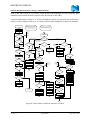
1
REFERENCE DESIGN
nRF24Z1 Headphone Reference
Design 1, nRF24Z1-HPR1
nRD24-02
GENERAL DESCRIPTION
The Nordic Semiconductor nRF24Z1 2.4GHz transceiver is the preferred device for use in
wireless CD quality audio streaming products like headphones for Compact Disk, MP3 and
Mini Disk.
To show the feasibility of nRF24Z1 in such products, a reference design system based on
nRF24Z1 has been designed featuring the same functions as one may expect to find in a
wireless portable headphone.
This document describes the nRF24Z1 Headphone Reference Design 1 (nRF24Z1-HPR1).
FEATURES
•
•
•
•
•
•
•
•
Audio transmitter (ATX) board with nRF24Z1, ADC, MCU, SMD antenna and
3.5mm jack female
Audio receiver (ARX) board with nRF24Z1, DAC, SMD antenna and 3.5mm jack
female
Six pushbutton user interface on ATX and ARX boards
ATX and ARX boards battery powered from two AAA cells
CD quality audio performance
10 meters line-of-sight range
Daughterboard featuring sockets for RS232 debugging, in-system programming of
MCU and updating nRF24Z1 EEPROM
All boards are manufactured on a 1.6mm thick, 2 layer FR4 substrate
Nordic Semiconductor ASA
Revision: 1.0
-
Vestre Rosten 81, N-7075 Tiller, Norway
Page 1 of 59
-
Phone +47 72 89 89 00
-
Fax +47 72 89 89 89
Date: January 2006
REFERENCE DESIGN
nRF24Z1 Headphone Reference Design 1, nRF24Z1-HPR1
TABLE OF CONTENTS
GENERAL DESCRIPTION .................................................................................................. 1
FEATURES............................................................................................................................ 1
1
Introduction .................................................................................................................... 4
2
Requirements.................................................................................................................. 5
3
Hardware system design................................................................................................. 6
3.1
ATX board.................................................................................................................. 6
3.2
ARX board ................................................................................................................. 6
3.3
Power supply and current consumption ..................................................................... 7
3.4
Power supply noise and audio quality considerations................................................ 7
3.5
Antenna considerations .............................................................................................. 8
3.6
Daughterboard .......................................................................................................... 10
4
Software system design ................................................................................................ 12
4.1
Look and Feel........................................................................................................... 12
4.2
Pairing, establishing a private address ..................................................................... 14
4.3
User Interface Buttons and LED .............................................................................. 16
4.4
Sleep Modes ............................................................................................................. 17
4.4.1
Automatic Power Down ................................................................................... 18
4.4.2
Wake-on-Interrupt ............................................................................................ 18
4.4.3
Wake-on-Timer ................................................................................................ 19
4.4.4
Interrupting MCU when Waking up ................................................................ 19
4.4.5
Audio Streaming Mode .................................................................................... 19
4.4.6
Wakeup from Automatic Power Down ............................................................ 19
4.5
User Interface Options ............................................................................................. 20
4.5.1
Full UI on ATX (User Interface Option 1) ...................................................... 20
4.5.2
Full UI on ARX (User Interface Option 2) ...................................................... 21
4.5.3
Full UI on ARX and ATX (User Interface Option 3) ...................................... 23
4.5.4
Identifying Sleep Modes in MCU Source Code............................................... 24
4.6
MCU Source Code ................................................................................................... 27
4.6.1
Definitions in hpref_defines.h............................................................... 28
4.6.2
Implementations in main.c and included files .............................................. 30
4.6.3
Implementations in z1slaveio.h and z1slaveio.c ............................. 30
4.6.4
Implementations in uartdebug.h and uartdebug.c ............................. 32
4.6.5
Implementations in adc.h and adc_wm8951.c ......................................... 33
4.6.6
Implementations in dac.h and dac_wm8711.c ......................................... 33
4.6.7
Implementations in mcu.h and mcu_atmega48_88.c ............................. 34
4.7
Setup of AVR Studio, STK500 and WinAVR......................................................... 36
4.8
Setup of EEPROM and z1config ............................................................................. 36
4.8.1
Full User Interface on ATX (User Option 1) ................................................... 37
4.8.2
Full User Interface on ARX (User Interface option 2)..................................... 37
4.8.3
Full User Interface on ATX and ARX (User Interface Option 3).................... 38
5
Reference design circuit schematics, PCB layout plots and BOM .............................. 40
5.1
ATX Board ............................................................................................................... 40
5.1.1
Schematics........................................................................................................ 40
5.1.2
Layout plots...................................................................................................... 44
5.1.3
Bill of Materials ............................................................................................... 45
5.2
ARX Board............................................................................................................... 48
Nordic Semiconductor ASA
Revision: 1.0
-
Vestre Rosten 81, N-7075 Tiller, Norway
Page 2 of 59
-
Phone +47 72 89 89 00
-
Fax +47 72 89 89 89
Date: January 2006
REFERENCE DESIGN
nRF24Z1 Headphone Reference Design 1, nRF24Z1-HPR1
5.2.1
Schematics........................................................................................................ 48
5.2.2
Layout plots...................................................................................................... 51
5.2.3
Bill of Materials ............................................................................................... 52
6
Daughterboard .............................................................................................................. 54
6.1
Daughterboard Schematic ........................................................................................ 54
6.2
Daughterboard Bill of Materials .............................................................................. 55
6.3
Small PCB with the Molex 53916-0208 connector Schematic................................ 55
7
References .................................................................................................................... 56
8
Your notes .................................................................................................................... 58
Nordic Semiconductor ASA
Revision: 1.0
-
Vestre Rosten 81, N-7075 Tiller, Norway
Page 3 of 59
-
Phone +47 72 89 89 00
-
Fax +47 72 89 89 89
Date: January 2006
REFERENCE DESIGN
nRF24Z1 Headphone Reference Design 1, nRF24Z1-HPR1
1
Introduction
This document describes the nRF24Z1-HPR1 reference design made by Nordic
Semiconductor to show the feasibility of the nRF24Z1 in wireless headphone applications.
Nordic Semiconductor provides the following for the reference design:
•
•
•
•
•
•
•
This document
Schematics in PDF and Altium Designer Protel 2004 format
PCB layout in Gerber and Altium Designer Protel 2004 format
Bill Of Material in PDF format
Microcontroller source code in C and as HEX file
z1config PC program
Hardware:
o Reference design audio transmitter (ATX) board
o Reference design audio receiver (ARX) board
o A Daughterboard used for in-system programming and debugging
o Flat Flexible Cable (FFC) with connector
o Nordic “EEPROM programmer USB dongle”
o USB cable
The first six items are available free of charge from Nordic Semiconductor’s web page,
http://www.nordicsemi.no
The design files and the hardware are intended as an aid to customers wanting to use the
nRF24Z1 in their own products. The published design files have been made so that only small
alternations (like form factor and placement of user interface buttons) are required to convert
them into production-ready files.
Nordic Semiconductor ASA
Revision: 1.0
-
Vestre Rosten 81, N-7075 Tiller, Norway
Page 4 of 59
-
Phone +47 72 89 89 00
-
Fax +47 72 89 89 89
Date: January 2006
REFERENCE DESIGN
nRF24Z1 Headphone Reference Design 1, nRF24Z1-HPR1
2
Requirements
In order to make full use of the Headphone Reference Design in your product development, a
certain level of knowledge and supporting programs and boards are required. These are listed
briefly here. Detailed setup information may be found in sections 4.7 and 4.8.
•
•
•
Knowledge of MCU programming in C is needed to perform modifications and
adoptions in the supplied source code. The source code is tested with the MCU and
user interface present on the reference design. If your hardware platform differs
significantly for this, modification of the C code is required.
The ADC and DAC chips used on the boards are supplied by Wolfson
Microelectronics. Nordic Semiconductor is not responsible for supporting Wolfson
products. Please consult the data sheets on
http://www.wolfsonmicro.com/products/digital_audio/dacs/WM8711/ and
http://www.wolfsonmicro.com/products/digital_audio/adcs/WM8951/.
If you choose to use the same MCU family (Atmel AVR), you will need to install
AVR Studio (http://www.atmel.com/dyn/products/tools_card.asp?tool_id=2725),
WinAVR (http://winavr.sourceforge.net/) and a terminal emulator, for example Tera
Term (http://www.ayera.com/teraterm/). All these programs are free of charge. You
will also need a means to do in-system programming of the MCU. For the Atmel AVR
family, use a STK500 development kit
(http://www.atmel.com/dyn/products/tools_card.asp?tool_id=2735) with an
atmega48V or atmega88V MCU. See section 4.7.
You will need a Nordic Semiconductor USB dongle to program the EEPROM. Download
files z1config_3_0_0.zip and nRF24Z1_firmware_2_0.hex from Nordic Semiconductor’s web
page (http://www/index.cfm?obj=product&act=display&pro=86). See section 4.8.
Nordic Semiconductor ASA
Revision: 1.0
-
Vestre Rosten 81, N-7075 Tiller, Norway
Page 5 of 59
-
Phone +47 72 89 89 00
-
Fax +47 72 89 89 89
Date: January 2006
REFERENCE DESIGN
nRF24Z1 Headphone Reference Design 1, nRF24Z1-HPR1
3
Hardware system design
The Headphone Reference Design consists of three parts; an audio transmitter (ATX) board;
an audio receiver (ARX) board; and a Daughterboard used for in-system programming and
debugging. The system is controlled by a microcontroller (MCU) located on the ATX board.
A user interface consisting of six pushbuttons and one LED is present on both ATX and ARX
boards. The design has been made in a way that allows easy modification of the user
interface.
All boards are manufactured on a 1.6mm thick, 2 layer FR4 substrate.
3.1
ATX board
The ATX board consists of a nRF24Z1 transceiver, a Fractus FR05-S1-N-0-102 chip antenna,
a Atmel Atmega48 MCU, a Wolfson WM8951L ADC, a configuration EEPROM, a
Daughterboard connector, user interface pushbuttons, user interface LED and two AAA
batteries. A 3.5mm female jack connects to an audio source, e.g CD or MP3 player. These
parts are all needed to implement the Headphone Reference Design, but in a finished product
several components may be omitted:
•
•
•
•
•
•
The Daughterboard connector is probably not needed because assembly will use preprogrammed MCU and EEPROM.
The MCU functionality may be executed on the host MCU of the audio source.
The contents of the configuration EEPROM may be offloaded to the MCU. This is a
matter of costs since the cost increase involved in a potential MCU upgrade might be
higher than the cost of the EEPROM chip.
The ADC is not needed if your source is digital.
The 3.5mm female jack connector may be replaced by a direct connection to an analog
audio source.
Not all 6 user interface pushbuttons may be required in your finished product.
The ATX board circuit schematics, PCB layout plots and Bill of Materials can be found in
chapter 5.1.
3.2
ARX board
The ARX board consists of a nRF24Z1 transceiver, a Fractus FR05-S1-N-0-102 chip antenna,
a WM8711L DAC, a configuration EEPROM, a Daughterboard connector, user interface
pushbuttons, user interface LED and two AAA batteries. A 3.5mm female jack is used for
connection to headphones or speakers. In the ARX board, cost and area reductions may
include:
•
The Daughterboard connector is probably not needed because the assembled
EEPROM will be pre-programmed.
Nordic Semiconductor ASA
Revision: 1.0
-
Vestre Rosten 81, N-7075 Tiller, Norway
Page 6 of 59
-
Phone +47 72 89 89 00
-
Fax +47 72 89 89 89
Date: January 2006
REFERENCE DESIGN
nRF24Z1 Headphone Reference Design 1, nRF24Z1-HPR1
•
•
The 3.5mm female jack connector may be replaced by a direct connection to
headphones.
Not all 6 user interface pushbuttons may be required in your finished product.
The ARX board circuit schematics, PCB layout plots and Bill of Materials can be found in
chapter 5.2.
3.3 Power supply and current consumption
The power supplies of the Headphone Reference Design ATX and ARX boards consist of
only two AAA batteries and linear regulators. ON/OFF switches have been added for “hard”
power on/off in addition to “soft” on/off in the user interface. A finished application may omit
the detachable AAA batteries and ON/OFF switch and rather use rechargeable batteries with
only “soft” power on/off. The power-on-reset effect of the ON/OFF switch may then be
replaced by a “reset” or “reconnect” button.
The Daughterboard is powered from the ATX or ARX board when it is connected. The USB
dongle output buffers receive its power supply from the same supply as the Daughterboard.
Table 3-1 below shows current (in mA) consumed from the two AAA batteries of the
complete ATX and ARX boards. The linear regulators are operating on 2.7V. For
explanations of Options 1, 2 and 3, please see section 4.5.
Option 1 ATX
ARX
Option 2 ATX
ARX
Option 3 ATX
ARX
On alone Streaming audio
1.5 mA
31.1 mA
2.9 mA
32.0 mA
2.9 mA
30.8 mA
2.6 mA
32.2 mA
4.3 mA
30.5 mA
5.0 mA
32.8 mA
User power down
1.1 mA
1.0 mA
2.1 mA
0.3 mA
3.2 mA
2.6 mA
Auto power down
0.9 mA
5.0 mA
1.5 mA
4.7 mA
2.8 mA
7.2 mA
Table 3-1 ARX and ATX boards current consumption
3.4
Power supply noise and audio quality considerations
Like in all electronic design the quality of the design is not only decided by the active devices
themselves, but also how they work together. Basically, there are two very important things to
look out for in a nRF24Z1 design:
•
•
Noise crosstalk through the power supply
Ground layout
The nRF24Z1 is a two-way package based radio, meaning it will constantly switch between
transmit-receive-transmit-receive and so on. In these two modes the current drawn will be
different, which may give rise to voltage ripple on the power supply. If this voltage ripple is
allowed to enter the analogue audio part of the design (ADC/DAC/CODEC), a constant 250430Hz tone might be present in the loudspeakers.
Nordic Semiconductor ASA
Revision: 1.0
-
Vestre Rosten 81, N-7075 Tiller, Norway
Page 7 of 59
-
Phone +47 72 89 89 00
-
Fax +47 72 89 89 89
Date: January 2006
REFERENCE DESIGN
nRF24Z1 Headphone Reference Design 1, nRF24Z1-HPR1
Hence, when nRF24Z1 is used in combination with ADC/DAC/CODECs, the nRF24Z1 must
be considered to belong to the digital domain. Because of this it is very important to avoid
power supply noise generated by nRF24Z1 (and other digital circuitry) from reaching the
analogue supply pins and reference voltage pins of the ADC/DAC/CODEC. Star-routing
directly from a low-noise supply source (e.g. a linear voltage regulator) is highly
recommended. The nRF24Z1 should have its own power supply line from the supply source.
The ADC/DAC/CODEC should also have their own separate digital and analogue supply
lines. In some designs an LC filter (serial inductor and shunt capacitor) on the analogue
supply line to the ADC/DAC/CODEC might also be required.
A power supply distribution strategy based on star-routing from a linear voltage regulator and
proper supply decoupling at the ADC/DAC/nRF24Z1 devices has been implemented on the
ATX and ARX boards of the Headphone Reference Design. Power supply distribution
strategy, supply decoupling, PCB layout and other important design issues for the nRF24Z1,
the Wolfson Microelectronics ADC (WM8951L) and DAC (WM8711L) have been carried
out as recommended in the datasheets and available application notes for each device:
•
•
•
“PCB layout and de-coupling guidelines” and “Application example” chapters in the
nRF24Z1 Product Specification
Application note nAN24-09 “nRF24Z1 RF layout” and the belonging RF layout
gerber files
Application notes from Wolfson microelectronics:
o WAN-0129, “Decoupling and Layout Methodology for Wolfson DACs, ADCs
and CODECs”
o WAN-0144, “Using Wolfson Audio DACs and CODECs with Noisy Supplies”
Good ground layout is just as important as the power supply distribution strategy to ensure the
best possible performance both from the nRF24Z1 and the ADC/DACs. In the Headphone
Reference Design ATX and ARX boards a PCB with two layers have been used. All available
areas on the top and bottom layers are flooded with ground plane. The top layer ground plane
areas are connected to the bottom layer ground plane areas through a large number of vias.
Please see the layout plots in chapter 5.1.2 and 5.2.2, and also the Headphone Reference
Design gerber files.
3.5
Antenna considerations
The antenna used on the ATX and ARX boards is the Fractus FR05-S1-N-0-102 chip SMD
antenna (http://www.fractus.com/img/ds_fr05_s1_n_0_102.pdf). The antenna has been placed
onto the ATX and ARX boards according to the recommendations given in the Fractus
antenna “User Manual” (document UM_FR05-S1-N-0-102) and application note “Wireless
Headsets” (document AN_FR05-S1-N-0-102). The Fractus User Manual and the application
note are available on request from Fractus (http://www.fractus.com).
Environmental factors that affect the antenna impedance and radiation properties are
parameters like shape of the PCB, size of available ground plane, proximity to housing,
housing material, proximity to human body etc.. Changing one or more of these parameters in
Nordic Semiconductor ASA
Revision: 1.0
-
Vestre Rosten 81, N-7075 Tiller, Norway
Page 8 of 59
-
Phone +47 72 89 89 00
-
Fax +47 72 89 89 89
Date: January 2006
REFERENCE DESIGN
nRF24Z1 Headphone Reference Design 1, nRF24Z1-HPR1
an application will change the antenna impedance and hence demand for a new matching
towards the antenna.
When designing with the Nordic nRF devices, the method to use is to initially base the
matching towards the antenna on the standard 50 ohm matching network as given in the nRF
device Product Specification. The antenna impedance is measured with the antenna placed in
the real application and with the application operating in its natural environments. If the
measured antenna impedance deviates significantly from 50 ohm, extra matching components
must be added in between our standard 50 ohm matching network and the antenna input to
make the antenna look like a 50 ohm load. In most situations you will be able to match
towards any antenna impedance by adding a PI-network (that is, shunt C or L - series C or L –
shunt C or L) in between our standard 50 ohm matching network and the antenna input.
Vector network analyzers are widely used for antenna impedance and VSWR (Voltage
Standing Wave Ratio) measurements. When measuring antenna impedance, the antenna must
be placed in the real application and the application must be operating in its natural
environments (e.g. hand-held, close to the ear etc.). After establishing the impedance value,
the graphical aid method of Smith chart is an effective way of designing the added impedance
matching network.
For the Headphone Reference Design ATX and ARX boards a 1.5pF shunt capacitor to
ground (C12 in the “RF Core” schematics, see Figure 5-1 and Figure 5-7) was needed for
optimal impedance matching towards the Fractus antenna in the 2.4GHz band. Figure 3-1
below shows the ATX board measured antenna impedance and VSWR with the board close to
the body and handheld for operation of the user interface push buttons. The measurements
were made with C12 = 1.5pF and with the rest of the matching network disconnected by
removing L3.
↑1 U
CH1 S11
1:
52.53
-j1.904 2.442 GHz
2:
33.30
1
j10.89
CH1 S11
LIN SWR 1 U/
REF 1 U
2.395125 GHz
0.5
3: 2 48.88
-j30.36
1:
1.092
2:
2.442
+400
MHzGHz
1.572 U
11 U
U
2.395125 GHz
3:
1.860
U
2.485125 GHz
2.485125 GHz
5
CAL
CAL
2
OFS
OFS
0
0.2
0.5
1
1
2
5
10
1 U/
CPL
CPL
3
-5
FIL
1k
FIL
1k
-2
-0.5
3
2
CENTER 2.442 GHz
Date:
29.NOV.05
1
1 U
-1
SPAN 1 GHz
100 MHz/
Date:
11:46:06
〈 1 U
CENTER 2.442 GHz
29.NOV.05
SPAN 1 GHz
11:47:00
VSWR
Antenna impedance
Figure 3-1 ATX board, measured antenna impedance and VSWR with two element matching
network
Due to the antenna radiation characteristics and to ensure sufficient harmonic suppression, a
change has been made in the matching network compared to what is given in the nRF24Z1
Nordic Semiconductor ASA
Revision: 1.0
-
Vestre Rosten 81, N-7075 Tiller, Norway
Page 9 of 59
-
Phone +47 72 89 89 00
-
Fax +47 72 89 89 89
Date: January 2006
REFERENCE DESIGN
nRF24Z1 Headphone Reference Design 1, nRF24Z1-HPR1
Product Specification. In the Headphone Reference Design capacitor C7 is changed from
1.5pF to 3.3pF. This increased value of C7 together with C12 = 0.8pF ensures good output
power at the fundamental, good harmonic suppression and at the same time good impedance
matching towards the antenna. Please see [3] and [4] and the “RF Core” schematics in Figure
5-1 and Figure 5-7.
Figure 3-2 below shows the ATX board measured antenna radiation patterns with horizontal
and vertical polarization. From these plots we can see that the radiation patterns are far from
omni-directional, and unfortunately this is often the situation in most practical designs.
Because of this, great care has to be taken when placing the antenna in a headphone design to
ensure that the direction of maximum radiation from both the ATX and ARX unit antennas is
pointing towards each other in most user situations. When using chip SMD antennas, please
follow the antenna manufacturers guidelines very closely as regards placement of the antenna
in the application and possible additional matching circuitry. Use the technical support
services available from the antenna manufacturer!
Horisontal Polarization
(Ref. Lev: +3.1dBm)
Vertical Polarization
(Ref. Lev: -1.7dBm)
Figure 3-2 ATX board, Antenna radiation patterns
3.6
Daughterboard
The Daughterboard features sockets for RS232 debugging, in-system programming of MCU
and updating nRF24Z1 EEPROM. In order to perform in-system programming and RS232
debugging, the Daughterboard has to be plugged onto either the ARX or ATX board. All
dongles and programming cables should be present in the Daughterboard during debugging
Nordic Semiconductor ASA
Revision: 1.0
-
Vestre Rosten 81, N-7075 Tiller, Norway
Page 10 of 59
-
Phone +47 72 89 89 00
-
Fax +47 72 89 89 89
Date: January 2006
REFERENCE DESIGN
nRF24Z1 Headphone Reference Design 1, nRF24Z1-HPR1
and programming. It also holds a RS232 level converter IC. An important thing to notice is
that the Daughterboard may not be used to read and write internal nRF24Z1 registers (like
z1config in conjunction with the nRF24Z1 Evaluation Boards). It only supports the EEPROM
features found under the “EEPROG” tab in z1config.
The Daughterboard consists of a printed circuit board (PCB) with RS232 and programming
headers. For connection between the Daughterboard Molex 52435-3072 connector (P1003)
and the ATX/ARX board Molex 54167-0208 connector (P501), a FFC (Flat Flexible Cable)
soldered to a small PCB with a Molex 53916-0208 connector (P1) has been made. The FFC
shall be inserted into the Daughterboard P1003 connector, and the P1 connector shall connect
to the ARX/ATX board P501 connector. When properly attached, the FFC points outwards
from the ARX and ATX boards. See the picture in Figure 3-3 below.
Figure 3-3 Daughterboard connection to ARX/ATX board
The Daughterboard circuit schematic and Bill of Materials can be found in chapter 6.
Schematic for the small PCB with the Molex 53916-0208 connector (P1) can also be found in
chapter 6.
Nordic Semiconductor ASA
Revision: 1.0
-
Vestre Rosten 81, N-7075 Tiller, Norway
Page 11 of 59
-
Phone +47 72 89 89 00
-
Fax +47 72 89 89 89
Date: January 2006
REFERENCE DESIGN
nRF24Z1 Headphone Reference Design 1, nRF24Z1-HPR1
4
4.1
Software system design
Look and Feel
When you first power on the Headphone Reference Design you will experience it from an end
user’s point of view. This section therefore explains what behavior to expect from the boards.
An audio source has to be plugged into the ATX board, and headphones into the ARX board.
Both the ATX and ARX boards have six pushbuttons and one power ON / OFF switch. In an
end application the power supply system would typically consist of a rechargeable battery and
charging electronics. But for simplicity the Headphone Reference Design ATX and ARX
boards are made with two AAA batteries and a power ON / OFF switch.
There are three different ways to implement a Soft Power ON button with the nRF24Z1.
These options are: 1) Soft Power ON at ATX only, not on ARX, 2) Soft Power ON at ARX
only, and 3) Soft Power ON at both ATX and ATX. The third option consumes more battery
power than the other options. It is important that you choose the option which is most suitable
for your design, as much of the Headphone Reference Design depends on this choice. Please
see section 4.5 for more detailed information about the three options.
Table 4-1 shows the placement of the user interface buttons on the ATX and ARX boards.
Volume
Up
Volume
Down
Play /
Soft Power ON
Stop /
Soft Power OFF
Next
Song
Previous
Song
Battery
ON / OFF
Table 4-1 Button placement on ARX and ATX board
When the boards are powered up (Battery ON / OFF switch), they broadcast on an initial
address. This address has to be chosen for your product or product family so that it will not
have any unwanted compatibility with a competitor’s product. Once the ATX and ARX are
both switched on and the user presses and holds the Play button, the ATX will generate a
random private address for the devices to use for the remaining time their battery power is
Nordic Semiconductor ASA
Revision: 1.0
-
Vestre Rosten 81, N-7075 Tiller, Norway
Page 12 of 59
-
Phone +47 72 89 89 00
-
Fax +47 72 89 89 89
Date: January 2006
REFERENCE DESIGN
nRF24Z1 Headphone Reference Design 1, nRF24Z1-HPR1
switched on.1 This means that at Battery power ON, any ATX may pair with any ARX within
a product family. (A product family is made up of ATX and ARX devices that all share a
common initial broadcast address, DAC chip, buttons definition and power saving scheme.)
After one set of ATX and ARX has paired on a private address, other devices in the same area
may be paired too. If you end up pairing with an unwanted device, simply switch off/on both
ARX and ATX to try again. If you want to create a new paired set within a product family,
simply switch off/on the two devices you want to pair up. All Headphone Reference Design
ATX units are produced equally. So are also all ARX units. (Please see section 4.2 for
flowcharts that illustrate the way pairing and the user interface works in the Headphone
Reference Design.
This dynamic pairing happening every time the units are turned on may be a feature in some
applications (product family, sharing an audio source with multiple headphones and HiFi
systems) and a problem in others (static systems). There are three other ways to perform
pairing:
•
•
•
Produce the ATX and ARX EEPROMs with equal and unique 40-bit addresses. This
will demand more from production and logistics. Also, if for example the ATX fails,
the ARX is useless to the consumer.
Produce all units with equal EEPROMs and perform pairing as the last stage of
production or as the first stage after the user powers the system on the first time. After
this the units will stay paired every time they are turned on. Without dynamic pairing,
units with this kind of pairing render both ATX and ARX useless if one of them fails.
This requires that the private address generated during pairing is programmed into the
EEPROM of the ARX. Information on how this is implemented is available from
Nordic Semiconductor support.
User intervention to choose address. Dip switches or digital selector wheels may be
used to select among a small selection of addresses. A microcontroller would be
needed to read the digital code and write it into the nRF24Z1 through its slave
interface.
The Headphone Reference Design uses dynamic pairing at every power up. So if you select
Battery OFF on one device, you must also select Battery OFF on the other one in order for
them to be paired again. The reason is that a device that was once paired and then had its
partner turned off will retain the private address it received and not go back to broadcasting
on the initial address before it is switched off/on. This is because it is hard for it to know
whether the partner was turned off or temporarily out of radio range. It is possible to add a
reset button to a nRF24Z1 device that will have the same effect as power cycling it. This,
however, has not been implemented on the Headphone Reference Design.
The Play and Stop buttons are inspired by those found on contemporary audio consumer
electronics products. There you typically see a CD player that powers down when the user
presses Stop. The CD player will power up and start playing again when the user presses Play.
In the Headphone Reference Design the Play button has to be pressed and held for some time
for the play command to be recognized across an RF link that is in power save mode. The
1
In one of the three user interface options (see section 4.5) the pairing will happen after
Battery power ON in both ATX and ARX without the user having to press the Play button.
Nordic Semiconductor ASA
Revision: 1.0
-
Vestre Rosten 81, N-7075 Tiller, Norway
Page 13 of 59
-
Phone +47 72 89 89 00
-
Fax +47 72 89 89 89
Date: January 2006
REFERENCE DESIGN
nRF24Z1 Headphone Reference Design 1, nRF24Z1-HPR1
Headphone Reference Design does not have a control link to the audio source. Therefore, all
buttons except Volume Up and Down will not affect the audio. However, the MCU source
code identifies insertion codes for audio source control sequences.
The Headphone Reference Design does not feature a control link to the audio source.
Therefore the music source must be activated manually. After the Play button has been
pressed and held to activate the ATX and ARX, subsequent use of the Play button will have
Pause functionality. When the audio is paused, the radio link is still active, and no power save
takes place. Pressing Play again will make the audio come back. Like a CD player, Play/Pause
have a shorter response time and higher power consumption than do Play/Stop. The Stop
button will put the ATX and ARX in sleep mode and cut off the music.
The Volume Up and Down buttons will increase or decrease the audio level. These buttons
may be held for continuous increase or decrease in audio level. The Next / Previous Song
buttons do not produce any result visible to the user. But the buttons are decoded in the MCU
source code, and may be used to control the audio source in an integrated product. All buttons
may be redefined in software. Every action that may need to control the audio source has been
identified in comments in the MCU source code. This may be turning on or pausing the audio
when Play is pressed, stopping it when Stop is pressed, moving forwards or backwards in the
music, etc.
4.2
Pairing, establishing a private address
The simplified flowcharts in Figure 4-1 and Figure 4-2 below illustrate the way pairing and
the user interface works in the Headphone Reference Design. As can be seen from the figures,
pairing (establishing a private address) only takes place once after a battery power off / on
cycle. That means that new audio connections can only be made between units that are
recently reset. User interface options 1 and 2 (see Figure 4-1) behave very similarly in that the
Play button must be pressed before the private address is established. It also needs the Play
button to be pressed in order to go back to audio streaming after the link is lost for a long
time. In option 1, only the ATX Play button will have the “Play***” effect on the figure. In
option 2, only the ARX Play button will have the “Play***” effect.
User interface option 3 (see Figure 4-2) finds a private address immediately after both ARX
and ATX are turned on. It automatically resumes playing music if a lost link is found again.
Both ATX and ARX Play buttons have full effect in option 3.
Nordic Semiconductor ASA
Revision: 1.0
-
Vestre Rosten 81, N-7075 Tiller, Norway
Page 14 of 59
-
Phone +47 72 89 89 00
-
Fax +47 72 89 89 89
Date: January 2006
REFERENCE DESIGN
nRF24Z1 Headphone Reference Design 1, nRF24Z1-HPR1
ATX
ARX
Insert
batteries
Insert
batteries
User: ON
User: Play***
User: ON
Establish
private
address
Receive
new private
address
Waiting
Link found
User: Volume up/down,
prev/next song etc.
Link found
User: Play***
Powerdown
Link lost
Awake
User: Stop
Receive
ATX
commands
Autodown
User: Play***
User: Play
User: Stop
Pause
=
mute
User: Volume up/down,
prev/next song etc.
Figure 4-1 Pairing, user interface options 1 and 2
Nordic Semiconductor ASA
Revision: 1.0
-
Vestre Rosten 81, N-7075 Tiller, Norway
Page 15 of 59
-
Phone +47 72 89 89 00
-
Fax +47 72 89 89 89
Date: January 2006
REFERENCE DESIGN
nRF24Z1 Headphone Reference Design 1, nRF24Z1-HPR1
ATX
ARX
Insert
batteries
Insert
batteries
User: ON
User: ON
Establish
private
address
Receive
new private
address
User: Volume up/down,
prev/next song etc.
Link found
User: Play
Powerdown
Link found
Link lost
Awake
Receive
ATX
commands
Autodown
Link found
User: Stop
User: Play
User: Stop
Pause
=
mute
User: Volume up/down,
prev/next song etc.
Figure 4-2 Pairing, user interface option 3
4.3
User Interface Buttons and LED
In the Headphone Reference Design 12 different buttons common in audio equipment have
been identified and supported in the MCU source code. These are: Play, Volume up, Volume
down, Stop, Skip forwards, Skip backwards, Scan forwards, Scan backwards, Bass boost,
Reconnect radio, Power, and Mute. Of these the following have been implemented on the
ATX and ARX PCBs:
•
Volume up: when pressed or held the DAC is instructed to increase the audio volume
Nordic Semiconductor ASA
Revision: 1.0
-
Vestre Rosten 81, N-7075 Tiller, Norway
Page 16 of 59
-
Phone +47 72 89 89 00
-
Fax +47 72 89 89 89
Date: January 2006
REFERENCE DESIGN
nRF24Z1 Headphone Reference Design 1, nRF24Z1-HPR1
•
•
•
•
•
Volume down: when pressed or held the DAC is instructed to decrease audio volume
Stop: brings the system into sleep mode
Play: when the system is in sleep mode, Play must be held for some time to wake the
system up. When the system is in audio streaming mode, Play may be used as a
play/pause/enter type button.
Skip forwards: may instruct audio source to go to next song
Skip backwards: may instruct audio source to go to previous song
All of this functionality is defined in software and may be redesigned for your product. As is
evident, the majority of the common control buttons are not supported on the ATX and ARX
PCBs. Also, the Headphone Reference Design has not been specified to pass commands onto
an audio source. For this the number of different audio sources is too large. However, the
MCU source code detects and decodes all 12 common audio buttons (and 3 more auxiliary
buttons) and lets you insert audio source control sequences for the buttons you choose to
include in your design. The power management source code also features comments stating
where audio source commands should be inserted.
Up to 15 buttons may easily be accommodated on an ARX PCB even without a
microcontroller on that side of the system. Please see schematic “ARX Board, RF Core” in
Figure 5-7 for an illustration of how diodes encode six buttons onto four pins in the
Headphone Reference Design. The button-to-input pin connections match the definitions
around line 64 in hpref_defines.h
If you choose to include fewer buttons than the Headphone Reference Design, simply omit
them from the schematics and comment out their function in the file included in main.c.
Unused input pins on the nRF24Z1 ARX should be grounded through resistors.
4.4
Sleep Modes
The nRF24Z1 features powerful mechanisms for power-control. This section describes the
available power modes and how they are selected for use in the Headphone Reference Design.
The ATX is put into sleep mode when the power down bit in TXMOD[6] is set to “1”.
Likewise, the ARX is put into sleep mode when the power down bit in RXMOD[7] is set to
“1”. Seen from the MCU or user, no attempt will be done to re-establish an audio link as long
as TXMOD[6] and RXMOD[7] are set. However, the status of ARX user interface buttons
will be forwarded to the ATX at whenever both are searching for a link at exactly the same
time.
To exit sleep mode, both TXMOD[6] and RXMOD[7] must be cleared. This must be done at
a point in time when the ATX nRF24Z1 is awake and ready to receive commands from the
MCU on its 2-wire or SPI slave interface. To exit sleep mode it is sufficient to update
TXMOD and RXMOD on the ATX side. No transfer registers (e.g. RXCSTATE) have to be
checked or set to exit sleep mode. RXMOD is sent from ATX to ARX whenever both are on
at the same time.
Nordic Semiconductor ASA
Revision: 1.0
-
Vestre Rosten 81, N-7075 Tiller, Norway
Page 17 of 59
-
Phone +47 72 89 89 00
-
Fax +47 72 89 89 89
Date: January 2006
REFERENCE DESIGN
nRF24Z1 Headphone Reference Design 1, nRF24Z1-HPR1
4.4.1
Automatic Power Down
In addition to the user setting the power down bits in TXMOD and RXMOD, the nRF24Z1
may automatically shut itself down when it looses its radio link for a certain time. This feature
is enabled in the ATX by writing a value ≠ 0x00 into TXWTI and in the ARX by writing a
value ≠ 0x00 into RXWTI. The power down bits in TXMOD and RXMOD will remain
cleared while in automatic power down. Therefore, the ATX and ARX will be able to reestablish a link any time they are within range and both searching for a link. The reason for
that the power down bits remain cleared is that they had to be cleared while streaming audio,
and when going to automatic power down, access to the nRF24Z1 control slave interface is
cut off.
The time that the devices will spend looking for a lost link before going to automatic power
down is specified by TXWTI · (TXLTI + 1) · 10ms in the ATX and RXWTI · (RXLTI + 1) ·
10ms in the ARX. The devices will only go to automatic power down from audio streaming
mode. When automatic power down is enabled, and after having lost its link for the specified
time, the devices will enter the sleep modes set by TXMOD, RXMOD, RXWAKE, TXWTI,
TXSTI, TXLTI, RXWTI, RXSTI and RXLTI. These registers may very well be set only once
in the EEPROM. They do not all need to be set by the MCU source code. The next two
sections will describe the two available sleep modes.
4.4.2
Wake-on-Interrupt
The nRF24Z1 may be programmed to stay in a low-power sleep mode until one or more of its
input pins change polarity. This is the sleep mode with the lowest current consumption. For
the ARX the interrupt source may be any combination of four general-purpose input pins. In
the Headphone Reference Design the input pin corresponding to the Play button is set as the
only interrupt source. General purpose input pins are available when the Slave Interface (SPI
or 2-wire connection to MCU) is disabled on the ARX.
For the ATX, only one input pin (DD[1]) is available as an interrupt source. On the
Headphone Reference Design this pin is an output from the MCU. That way the MCU may
poll (or be interrupted by) the user interface buttons on its own input pins and then consider
whether or not to interrupt and wake up the ATX. If the right button is pressed, the MCU may
interrupt the nRF24Z1 to wake it up. This is beneficial, as the MCU is better suited than a
user at maintaining DD[1] hold time.
Please note that both positive and negative edges on the selected input pins will trigger
interrupts in the nRF24Z1.
After waking from an interrupt, the ATX will try to establish a radio link for TXWTI ·
(TXLTI + 1) · 10ms. If this fails, the ATX will go back to sleep mode. Similarly, if a pin
change is detected on the selected pin(s), the ARX will try to establish a radio link for
RXWTI · (RXLTI + 1) · 10ms. If this fails, the ARX will go back to sleep mode.
Nordic Semiconductor ASA
Revision: 1.0
-
Vestre Rosten 81, N-7075 Tiller, Norway
Page 18 of 59
-
Phone +47 72 89 89 00
-
Fax +47 72 89 89 89
Date: January 2006
REFERENCE DESIGN
nRF24Z1 Headphone Reference Design 1, nRF24Z1-HPR1
4.4.3
Wake-on-Timer
An internal, low-power, timer in the nRF24Z1 may be used to make it try to establish a radio
link at regular intervals. While trying to establish a link, the SPI or 2-wire slave control
interface is active. During this time the MCU will be able to access nRF24Z1 registers.
The time spent trying to establish a radio link is TXWTI · 10ms for the ATX and RXWTI ·
10ms for the ARX. The time spent sleeping between such attempts is (TXSTI_1 · 256 +
TXSTI_0) · 10ms in the ATX and (RXSTI_1 · 256 + RXSTI_0) · 10ms in the ARX. The time
spent trying to establish a radio link is connected to the number of channels used for linkup
(NLCH). R/TXWTI < 0x02 should only be used with NLCH = 0x0F.
Wake-on-Timer may not be combined with Wake-on-Interrupt inside the same chip. The
sleep mode for the ATX is selected in TXMOD while the sleep mode for the ARX is selected
in RXMOD and RXWAKE.
4.4.4
Interrupting MCU when Waking up
The nRF24Z1 has several ways of interrupting an external MCU or other electronics. The
Headphone Reference Design only uses one interrupt, and it only uses it on the ATX. The
wakeup from power down interrupt is the only interrupt whose interrupt flag does not have to
be cleared in INTSTA. Enabling the wakeup from power down interrupt on the ATX makes
the nRF24Z1 IRQ output pin track the sleep modes of the nRF24Z1. An active low IRQ pin
will be low when the ATX nRF24Z1 is streaming audio or trying to establish a link. It will be
high when the ATX nRF24Z1 is waiting between attempts at establishing a link. Through
being interrupted by this pin (or polling it) the MCU will know when the SPI or 2-wire slave
control interface of the nRF24Z1 may be accessed.
This also means that if the ATX is Wake-on-Timer, the external MCU does not have to be in
charge of system timing while in sleep mode. Instead the MCU is interrupted by the ATX
nRF24Z1 whenever it wakes up and becomes ready to receive commands. However, since the
nRF24Z1 units may also wake up from automatic power down, or for some other reason cease
generating interrupts, it is important that the MCU has a backup clock that makes sure the
system does not hang if an expected interrupt should not occur.
4.4.5
Audio Streaming Mode
This is the normal operation of the system; audio content is streamed from the ATX to the
ARX. While in Audio Streaming Mode, the MCU in the Headphone Reference Design will
use its own watchdog interrupt in order to keep track of time. At regular intervals the MCU
polls the user interface buttons on the ARX and ATX. Depending on which button is pressed,
the MCU takes the appropriate action.
4.4.6
Wakeup from Automatic Power Down
Because automatic power down may put ATX and/or ARX into either wake-on-interrupt or
wake-on-timer, different mechanisms are needed to bring the devices out of automatic power
Nordic Semiconductor ASA
Revision: 1.0
-
Vestre Rosten 81, N-7075 Tiller, Norway
Page 19 of 59
-
Phone +47 72 89 89 00
-
Fax +47 72 89 89 89
Date: January 2006
REFERENCE DESIGN
nRF24Z1 Headphone Reference Design 1, nRF24Z1-HPR1
down. A device set to wake-on-interrupt has to be interrupted (i.e. Play button pressed) before
it starts trying to re-establish a link. A device set to wake-on-timer will check for a link on a
regular basis. If both ARX and ATX are wake-on-timer, and the sleep/wake times are set
correctly, they will automatically wakeup from automatic power down.
Please note that the power down bits in RXMOD and TXMOD must both be cleared for the
system to be able to wake up from automatic power down. However, as stated above, if the
user has chosen to power off the system, the power down bits in RXMOD and TXMOD will
be set, and the units will not power on even if they are both searching for a link at the same
time.
4.5
User Interface Options
There are three fundamental ways to design a user interface around the nRF24Z1. They differ
in the sleep modes they use. The three options are:
1. Full user interface on ATX, every UI function except power on at ARX
2. Full user interface on ARX, every UI function except power on at ATX
3. Full user interface on both ARX and ATX.
The options will be explained in more detail in the following sections. The three options are
implemented in main_option1.c, main_option2.c and main_option3.c. The
Headphone Reference Design is set up with User Interface Option 3. The other modes can be
tried out by changing main.c and reprogramming the EEPROMs according to the
description in the top of the main_optionX.c file. Please also see section 4.8 for more
information about reprogramming EEPROMs. When you change the user interface option, the
project will have to be recompiled, and the resulting main.hex must be programmed into
the ATX MCU by means of a STK500 (or similar device for your chosen MCU).
4.5.1
Full UI on ATX (User Interface Option 1)
With this option, ATX is wake-on-interrupt while ARX is wake-on-timer. This ensures very
low power consumption in the ATX. But the ATX will only wake up when the user presses
the Play button on ATX. There is thus no way to pass a command from ARX to ATX while
the system is in sleep mode. The ARX will occasionally try to establish a link. This will
succeed if the units are within range when the ATX is interrupted. Wakeup from automatic
power down requires user interaction on the ATX.
A typical application example is a wireless headphone with limited user interface. Today’s
wired headphones rarely have user interfaces on them. Figure 4-3 shows a flowchart of this
user interface option.
Nordic Semiconductor ASA
Revision: 1.0
-
Vestre Rosten 81, N-7075 Tiller, Norway
Page 20 of 59
-
Phone +47 72 89 89 00
-
Fax +47 72 89 89 89
Date: January 2006
REFERENCE DESIGN
nRF24Z1 Headphone Reference Design 1, nRF24Z1-HPR1
ARX is on, auto power down after
searching for a link for 500ms. It then
searches for a link for 10ms and sleeps
for 480ms on wake-on-timer, RXMOD
must not be changed for initial ARX
power on
MCU startup
ATX goes straight to power down with
wake-on-interrupt, TXMOD must be
altered for initialATX power on
Power down ADC
1
Play pressed on
MCU?
User must
press
Play on
ATX for
MCU to
exit loop
Yes
Wake ATX nRF24Z1
with interrupt from MCU
Wait for ATX interrupt or
MCU timeout
powermode = =
PMODE_AUTODOWN
PMODE_AWAKE
Alter TXMOD for power
up
PMODE_POWERDOWN
Wait for linkup
Play pressed on
MCU?
No
Link found?
Yes
No
Wake ATX nRF24Z1
with interrupt from MCU
Put ATX nRF24Z1 back
to wake-on-interrupt
Wait for linkup
User
wakes
system
from
automatic
sleep
mode
wakeup = =
WAKE_WAIT
Play pressed on
MCU?
wakeup = =
WAKE_Z1_INT
WAKE_Z1_INT
Not supposed to receive
interruptts from ATX
nRF24Z1
Not supposed to receive
interruptts from ATX
nRF24Z1
1
1
WAKE_WAIT
ATX nRF24Z1 shut
down?
No
Wait to poll again
Yes
Link found?
Yes
Button pressed on
ARX?
Yes
Wake ATX nRF24Z1
with interrupt from MCU
No
Run user
interface
Insert audio source off
sequence
No
1
Ready to receive
private address?
Yes
Yes
Set new private address
No
1
Insert audio source on
sequence
No
Wait for linkup
Wake up ADC
Disable ATX auto power
down
Automatic
power
down
detected
Power down ADC
Alter TXMOD for power
up
Yes
Consider ARX buttons
powermode =
PMODE_AUTODOWN
Alter RXMOD to attempt
power up
Consider ATX buttons
User puts
system
into sleep
mode
1
No
powermode =
PMODE_AWAKE
Link found?
Wait for linkup
User
bring
system
out of
sleep
mode
1
Yes
Power on remote DAC
Link found?
Stop pressed?
Yes
Volume up
pressed?
Insert audio source off
sequence
No
No
Yes
Power down ARX
Increase volume
DAC success?
Power down DAC
Power down ARX
No
No
Enable ATX auto power
down
Power down ATX
Yes
Wake up ADC
Power down ATX
Wake up DAC
1
Yes
Volume down
pressed?
Power down ADC
Yes
powermode =
PMODE_POWERDOWN
Decrease volume
DAC success?
No
No
Insert audio source on
sequence
Yes
MCU program
terminates
Unmute ARX
Other button
pressed?
Wake up ADC
Wake up DAC
Yes
powermode =
PMODE_AWAKE
No
powermode =
PMODE_AWAKE
Insert audio source
control sequence
1
Enable ATX auto power
down
Logical deboune
1
1
Figure 4-3 Flow chart of full user interface on ATX
4.5.2
Full UI on ARX (User Interface Option 2)
Very low power consumption in the ARX can be achieved if it is set to be wake-on-interrupt
while in sleep mode. The ATX is wake-on-timer. That means that the ARX will only wake up
when the user presses the Play button there. There is no way to pass information from the
Nordic Semiconductor ASA
Revision: 1.0
-
Vestre Rosten 81, N-7075 Tiller, Norway
Page 21 of 59
-
Phone +47 72 89 89 00
-
Fax +47 72 89 89 89
Date: January 2006
REFERENCE DESIGN
nRF24Z1 Headphone Reference Design 1, nRF24Z1-HPR1
ATX to the ARX while in sleep mode. (Only RXPIN and RXMOD are sent.) Wakeup from
automatic power down therefore requires user interaction on the ARX.
A typical application example is a wireless headphone which is worn while the audio source
(player) is not available to the user. A remote control on the headphone is therefore desirable.
MCU startup
ATX is wake-on-timer, it goes to
automatic power down after 1000ms
without link. During this time MCU has
access to ATX nRF24Z1.
Power down ADC
Prepare ARX to power
up
User must
press
Play on
ARX for
MCU to
exit loop
ATX nRF24Z1
active?
Yes
Link found?
ARX goes directly to wake-on-interrupt.
RXMOD must be set at a later stage in
order for it to be able to power up.
1
Wait for ATX interrupt or
MCU timeout
powermode = =
PMODE_AUTODOWN
PMODE_AWAKE
User presses Play on
ARX, wakes system PMODE_POWERDOWN
from auto sleep mode
No
ATX nRF24Z1
active?
No
wakeup = =
WAKE_Z1_INT
Wait to poll again
Yes
wakeup = =
WAKE_WAIT
Automatic
power down
detected
WAKE_Z1_INT
No
ATX is wake-on-timer,
something is wrong if an
entire MCU safety wait
period elapsed
1
Yes
Ready to receive
private address?
ATX nRF24Z1
active?
WAKE_WAIT
Insert audio source off
sequence
Run user
interface
No
Power down ADC
No
1
Link found?
Yes
Set new private address
1
powermode =
PMODE_AUTODOWN
Yes
No
Button pressed on
ARX?
No
Wait for linkup
1
1
Yes
Insert audio source on
sequence
Link found?
No
Button pressed on
ARX?
Consider ATX buttons
Yes
Yes
Consider ARX buttons
Yes
No
Power on remote DAC
powermode =
PMODE_AWAKE
Consider ARX buttons
User puts
system
into sleep
mode
User brings
system out of
sleep mode
Wake up ADC
Play pressed?
No
Stop pressed?
DAC success?
No
Yes
1
1
Yes
Wake up ADC
Yes
Volume up
pressed?
No
Disable ATX auto power
down
Wake up DAC
Insert audio source off
sequence
Yes
Power down DAC
Increase volume
Alter TXMOD for power
up
Power down ARX
No
DAC success?
Power down ATX
No
Yes
Unmute ARX
Alter RXMOD to attempt
power up
Yes
Volume down
pressed?
Power down ADC
Yes
powermode =
PMODE_POWERDOWN
Wait for linkup
Insert audio source on
sequence
powermode =
PMODE_AWAKE
Decrease volume
Link found?
Wake up ADC
No
1
No
MCU program
terminates
Wake up DAC
Other button
pressed?
Power down ARX
Enable ATX auto power
down
powermode =
PMODE_AWAKE
Yes
Power down ATX
Enable ATX auto power
down
1
1
No
Insert audio source
control sequence
Logical deboune
1
Figure 4-4 Flow chart of full user interface on ARX
Nordic Semiconductor ASA
Revision: 1.0
-
Vestre Rosten 81, N-7075 Tiller, Norway
Page 22 of 59
-
Phone +47 72 89 89 00
-
Fax +47 72 89 89 89
Date: January 2006
REFERENCE DESIGN
nRF24Z1 Headphone Reference Design 1, nRF24Z1-HPR1
4.5.3
Full UI on ARX and ATX (User Interface Option 3)
A full user interface on both ARX and ATX can be achieved at the cost of increased power
consumption in sleep mode. In order to pass information like power-on commands both ways
between ARX and ATX, both have to be wake-on-timer while in sleep mode. The timer
parameters are set so that one unit (typically the ARX) is looking for a link for a very short
time and then sleeps for a somewhat longer time before looking for a link again. The other
unit (typically the ATX) is slower and looks for a link for more than the duration of an
awake+asleep period of the faster unit. The sleep period of the slow unit will therefore
become rather long. A trade off exists between the power consumption while in sleep mode
and the time the user has to press and hold the Play button for music to appear. In the
Headphone Reference Design, both ARX and ATX use a 10% on-time while in sleep mode.
The user then has to hold the Play button for more than two seconds.
However, a benefit of both units being wake-on-timer is that recovery from auto power down
will be automatic and not require user intervention.
Nordic Semiconductor ASA
Revision: 1.0
-
Vestre Rosten 81, N-7075 Tiller, Norway
Page 23 of 59
-
Phone +47 72 89 89 00
-
Fax +47 72 89 89 89
Date: January 2006
REFERENCE DESIGN
nRF24Z1 Headphone Reference Design 1, nRF24Z1-HPR1
MCU startup
ATX is wake-on-timer, it goes to
automatic power down after 500ms
without link. ATX has a very sluggish
wake/sleep pattern
Power down ADC
ARX is wake-on-timer, it goes to
automatic power down after 520ms
without link. ARX has a very fast wake/
sleep pattern
No user
interaction
needed, devices
only have to be
in range
ATX nRF24Z1
active?
Y
e
s
Link found?
1
Wait for ATX interrupt or
MCU timeout
powermode = =
PMODE_AUTODOWN
No
Both units
are within
range
No
PMODE_AWAKE
PMODE_POWERDOWN
Wait to poll again
ATX nRF24Z1
active?
Yes
wakeup = =
WAKE_Z1_INT
wakeup = =
WAKE_WAIT
Automatic
power down
detected
WAKE_Z1_INT
No
Ready to receive
private address?
ATX is wake-on-timer,
something is wrong if an
entire MCU safety wait
period elapsed
1
Yes
ATX nRF24Z1
active?
WAKE_WAIT
Insert audio source off
sequence
Run user
interface
Yes
Power down ADC
Set new private address
No
No
1
Link found?
1
Wait for linkup
powermode =
PMODE_AUTODOWN
Yes
No
1
Link found?
1
Yes
Yes
No
Button pressed on
ARX?
No
No
Button pressed on
ARX?
Consider ATX buttons
Yes
Insert audio source on
sequence
Yes
Power on remote DAC
Consider ARX buttons
User puts
system to
sleep
mode
No
Wake up ADC
DAC success?
powermode =
PMODE_AWAKE
Power down DAC
No
Button pressed on
ATX?
Yes
Consider ARX buttons
Stop pressed?
Yes
1
Yes
Power down ARX
Consider ATX buttons
Volume up
pressed?
User brings
system out of
sleep mode
Insert audio source off
sequence
Power down ATX
Yes
Play pressed?
powermode =
PMODE_POWERDOW
N
1
Power down DAC
Increase volume
Power down ARX
No
No
No
Power down ATX
1
Yes
Insert audio source on
sequence
Disable ATX auto power
down
Volume down
pressed?
Power down ADC
Yes
powermode =
PMODE_POWERDOWN
Decrease volume
Yes
Alter TXMOD for power
up
Wake up ADC
No
Wake up DAC
MCU program
terminates
No
Power down ARX
Alter RXMOD to attempt
power up
Other button
pressed?
Unmute ARX
Wait for linkup
powermode =
PMODE_AWAKE
Enable ATX auto power
down
Yes
No
Insert audio source
control sequence
Link found?
Power down ATX
Enable ATX auto power
down
1
1
Logical deboune
1
Figure 4-5 Flow chart of full user interface on both ARX and ATX
4.5.4
Identifying Sleep Modes in MCU Source Code
In User Interface modes 2 and 3, the ATX nRF24Z1 is set up to use the Wake-on-Timer sleep
mode. Thus the MCU will receive an interrupt from the IRQ pin whenever the ATX nRF24Z1
wakes from sleep and tries to establish a link. An important thing to notice is that this will
Nordic Semiconductor ASA
Revision: 1.0
-
Vestre Rosten 81, N-7075 Tiller, Norway
Page 24 of 59
-
Phone +47 72 89 89 00
-
Fax +47 72 89 89 89
Date: January 2006
REFERENCE DESIGN
nRF24Z1 Headphone Reference Design 1, nRF24Z1-HPR1
happen both when the MCU actively put the ATX nRF24Z1 into Wake-on-Timer sleep mode
and when the ATX nRF24Z1 entered automatic power down.
The MCU program is of course able to know which commands it sent the ATX nRF24Z1, and
which mode the system is in. If the MCU receives an interrupt while being in Audio
Streaming mode, the ATX nRF24Z1 has gone into automatic power down. This is only the
case when the ATX nRF24Z1 goes to Wake-on-Timer when it automatically powers down.
When an automatic power down is detected, the MCU will power down the ADC (but not the
DAC because the control link is down). It will also power down itself.
In User Interface Option 1 the ATX nRF24Z1 does not generate interrupts to the MCU when
powering up. But the interrupt pin ceases to be active when the ATX nRF24Z1 goes to
automatic power down. Hence this is detected by the MCU by polling the ATX nRF24Z1
interrupt pin.
The opposite of entering automatic power down is coming out of automatic power down.
When this happens, the MCU will have noticed that the system went to automatic power
down at an earlier stage. The interrupts that occur in User Interface Options 2 and 3 during
wake-on-timer sleep mode will cease to occur. The MCU will therefore have to rely on
another wakeup source in addition to the external interrupt. This additional wakeup source is
its watchdog interrupt. If in sleep mode and a certain wait period ends before the MCU
receives the external interrupt, the MCU checks if the nRF24Z1 system did just establish a
link. If this is the case, the MCU will power up the ADC and itself.
In User Interface Option 1 the ATX is wake-on-interrupt. An interrupt is sent from the MCU
to the ATX nRF24Z1 when the MCU detects that the user is pressing the ATX Play button.
After receiving the interrupt, the ATX nRF24Z1 will try to establish a link for TXWTI ·
(TXLT1 + 1) · 10ms. During this time the MCU will figure out if the ATX and ARX were
able to establish a link. If they did, the system goes out of automatic power down.
The sleep mode (variable powermode) can be either PMODE_POWERDOWN,
PMODE_AUTODOWN or PMODE_AWAKE. The wakeup source (variable wakeup) can be
either WAKE_Z1_INT or WAKE_WAIT. Table 4-2 below shows the different combinations as
they are used in User Interface Options 2 and 3. Table 4-3 shows the meanings of the
combinations in User Interface Option 1.
powermode
PMODE_POWERDOWN
Nordic Semiconductor ASA
Revision: 1.0
-
wakeup
WAKE_Z1_INT
Sleep mode
Normal sleep mode; ATX nRF24Z1 is waking
up the MCU by means of an interrupt. The
MCU will then check if a power on command
(Play button) is received from the user
interface. If such a command is received, the
MCU powers on itself, the ADC, the ATX and
the ARX before setting
powermode=PMODE_AWAKE
Vestre Rosten 81, N-7075 Tiller, Norway
Page 25 of 59
-
Phone +47 72 89 89 00
-
Fax +47 72 89 89 89
Date: January 2006
REFERENCE DESIGN
nRF24Z1 Headphone Reference Design 1, nRF24Z1-HPR1
PMODE_POWERDOWN
WAKE_WAIT
PMODE_AUTODOWN
PMODE_AUTODOWN
WAKE_Z1_INT
WAKE_WAIT
PMODE_AWAKE
WAKE_Z1_INT
PMODE_AWAKE
WAKE_WAIT
System is asleep but no interrupt is received
from ATX nRF24Z1 before the MCU safety
period times out. This is a faulty condition if
ATX is Wake-on-Timer.
If the ATX is currently on (i.e. trying to or
succeeding in establishing a link), check if a
link is present. If it is, exit auto power down by
powering up the ADC and setting
powermode=PMODE_AWAKE
System is streaming audio but an interrupt is
received. This indicates that the ATX nRF24Z1
went to Wait-on-Timer sleep mode. I.e. the
ATX went to automatic power down. The MCU
subsequently puts into sleep mode the units it
can reach (ADC and itself). It then sets
powermode=PMODE_AUTODOWN
Normal audio streaming mode; both nRF24Z1
units are on. MCU wakes up periodically from
its internal watchdog timer interrupt to poll the
user interface for actions to be made. If the Stop
button is pressed, the MCU powers down the
system and sets
powermode=PMODE_POWERDOWN
Table 4-2 Combinations in User Interface Options 2 and 3
powermode
PMODE_POWERDOWN
wakeup
WAKE_Z1_INT
PMODE_POWERDOWN
WAKE_WAIT
PMODE_AUTODOWN
PMODE_AUTODOWN
WAKE_Z1_INT
WAKE_WAIT
PMODE_AWAKE
WAKE_Z1_INT
Nordic Semiconductor ASA
Revision: 1.0
-
Sleep mode
Faulty state as no interrupts should be sent from
ATX nRF24Z1 to MCU. ATX is wake-oninterrupt, i.e. it will receive an interrupt to wake
up, not generate one.
System is in sleep mode, MCU polls buttons for
wakeup command. If ATX Play button is
pressed, try to wake up system. If wakeup
succeeds, set powermode=PMODE_AWAKE
The system went to automatic power down.
Check if ATX Play button is being pressed. If it
is, try to establish a link and wake up system. In
the case of linkup success, set
powermode=PMODE_AWAKE
Faulty state as no interrupts should be sent from
ATX nRF24Z1 to MCU.
Vestre Rosten 81, N-7075 Tiller, Norway
Page 26 of 59
-
Phone +47 72 89 89 00
-
Fax +47 72 89 89 89
Date: January 2006
REFERENCE DESIGN
nRF24Z1 Headphone Reference Design 1, nRF24Z1-HPR1
PMODE_AWAKE
WAKE_WAIT
Normal audio streaming mode; both nRF24Z1
units are on. MCU wakes up periodically from
its internal watchdog timer interrupt to poll the
user interface for actions to be made. If the Stop
button is pressed, the MCU powers down the
system and sets
powermode=PMODE_POWERDOWN. But
before reading the remote and local buttons the
MCU checks whether or not the ATX nRF24Z1
went to automatic power down. If that was
detected, the MCU sets
powermode=PMODE_AUTODOWN.
Table 4-3 Combinations in User Interface Option1
Most of main.c deals with the different sleep modes. powermode is a local variable in
main.c. wakeup is a global variable written in mcu_wait_ms() and
SIGNAL(SIG_INTERRUPT0) in mcu_atmega48_88.c.
4.6
MCU Source Code
This section will describe the main features of the MCU source code. The MCU source code
is best understood if you start reading in the following order before making any alterations or
attempting to compile it:
1. This document
2. hpref_defines.h
3. main.c and the file included in it
The MCU source code is written in a modular fashion. Here is a brief description of what the
different files do:
•
•
•
•
•
•
hpref_defines.h: Top-level definitions for the entire MCU source code. All
preprocessor #define statements should be put in this file unless they are hardware
dependant or better understood in the context where they are used.
main.c: Top-level container for linkup and user interface. This file includes the code
that receives and decodes interaction with the user, power-down modes and pairing.
main_optionX.c: Power down modes, user interface, main program. X=1, 2, or 3.
z1slaveio.h and z1slaveio.c: Communication between the MCU and the
nRF24Z1 chips. Functions defined in z1slaveio.h provide low-level and midlevel read and write operations.
uartdebug.h and uartdebug.c: Debug information to be used while developing
the MCU source code. Functions declared in uartdebug.h are not used in code
compiled for production versions of the product.
adc.h: Declaration of functions that all ADCs must support. This file is hardware
independent.
Nordic Semiconductor ASA
Revision: 1.0
-
Vestre Rosten 81, N-7075 Tiller, Norway
Page 27 of 59
-
Phone +47 72 89 89 00
-
Fax +47 72 89 89 89
Date: January 2006
REFERENCE DESIGN
nRF24Z1 Headphone Reference Design 1, nRF24Z1-HPR1
•
•
•
•
•
•
4.6.1
adc_wm8951.c: Hardware-dependent implementation of the functions declared in
adc.h. This file is written for the Wolfson WM8951L ADC. It (and not adc.h)
must be ported if you choose to design with a different ADC.
dac.h: Declaration of functions that all DACs must support. This file is hardware
independent.
dac_wm8711.c: Hardware-dependent implementations of the functions declared in
dac.h. This file is written for the Wolfson WM8711 DAC. It (and not dac.h) must
be ported if you choose to design with a different DAC.
mcu.h: Declarations of functions that must be rewritten if a different MCU is used.
This file is hardware-independent.
mcu_atmega48_88.c: Implementation of hardware-dependent MCU functions for
the Atmel Atmega48 and Atmega88 ICs. (These ICs are identical except for the size of
their flash memory.) Architecture-dependent #include <…> statements are featured
at the top of mcu_atmega48_88.h. This file must be ported if you choose to
design with a different MCU.
makefile: Project-wide makefile for compilation with AVRGCC. You must rewrite
this file if you want to use a different compiler or MCU family. The processor type is
defined in the beginning of makefile.
Definitions in hpref_defines.h
For MCU speed, define one of the following:
//#define MCU_8000
//#define MCU_3686
#define MCU_1000
// Either 8MHz internal RC oscillator
// Or STK500 3.686MHz oscillator
// Or 8MHz RC osc. divided by 8, default in atmega48/88
If you use a development board to develop your application, and this board has differing logic
levels etc. from those of your finished product, choose your compilation target here. For the
Headphone Reference Design, the ATX and ARX boards have active high buttons and LEDs
and converters that need setup sequences. The nRF24Z1 evaluation board and the STK500
have active low buttons and LEDs combined with intant-on audio converters. Another
important difference is that the nRF24Z1 on the ATX evaluation board is I2S slave while it is
I2S master on the Headphone Reference Design. This must be set in the EEPROM.
//#define ATXDEVBOARD
//#define ARXDEVBOARD
// ATX is development board, not finished product
// ARX is development board, not finished product
The Headphone Reference Design uses the 2-wire slave interface of the ATX nRF24Z1.
When 2-wire is selected, certain other parameters may be defined as well.
#define Z12WDEVADR
0b00101001
//#define Z12WDEVADR
0b01101001
#define TERMINATE_ON_ERROR
// Either nRF24Z1 slave dev. adr, SADR=0
// Or nRF24Z1 slave dev. adr, SADR=1
// Halt program at unexpected state
The Headphone Reference Design has a built-in debugging system. Selecting to compile it in
will increase your compiled image size while offering you more control over your application
development. There are multiple levels of debugging which may be turned on and off at
compile time.
Nordic Semiconductor ASA
Revision: 1.0
-
Vestre Rosten 81, N-7075 Tiller, Norway
Page 28 of 59
-
Phone +47 72 89 89 00
-
Fax +47 72 89 89 89
Date: January 2006
REFERENCE DESIGN
nRF24Z1 Headphone Reference Design 1, nRF24Z1-HPR1
#define DEBUG
#ifdef DEBUG
#define DEBUG2W
//#define DEBUGIF
//#define DEBUGDAC
#define Z1UI
//#define ADCUI
//#define DACUI
#endif
//
//
//
//
//
//
//
//
Enable debug information to terminal with UART
If the debug system and...
Enable debug of 2-wire interface
Enter interactive debug interface at bootup
Report RXEXEC status from DAC writes
Either enable nRF24Z1 ATX r/w in debug interface
Or enable ADC write-only in debug interface
Or enable DAC write-only in debug interface
Global project defines let you choose which parts of this program to compile into your MCU.
Reducing the feature set will reduce the memory requirement. Different API functions may be
selectively included in your program. Please see explanation below.
#define Z1INTERRUPT
#define Z1ALTERADDRESS
// Enable interrupt from nRF24Z1 to MCU
// Enable address changes
The user interface (man-machine interface) may be configured by means of several defines.
The most important choice is which option to include in main.c.
#define USELED
#ifdef USELED
#define LEDON
#define LEDOFF
#define LED_INITIAL
#define LED_FAILURE
#define LED_AWAKE
#define LED_POWERDOWN
#define LED_AUTODOWN
#endif
// Use LEDs
// If LEDs are used, define some particulars:
0x01
// IO definition: turn LED on
0x00
// IO definition: turn LED off
0b1111111111111111; // Initial blink sequence
0b0001000100010001; // Blink if failure
0b1010000000000000; // Blink if awake
0b1000000010000000; // Blink if power down
0b1000000010000000; // Blink if automatic power down
User interface buttons are located on both ATX and ARX. The definitions below map out the
physical encoding of ARX buttons through DI[0..3] pins and into the RXPIN register. The
same encoding is used by the MCU to describe the buttons pressed on its GPIO pins. That
way the same code is processing both ATX and ARX buttons. In the Headphone Reference
design, all buttons are active high. In your design, tie unused ARX DI pins to ground by
means of resistors. Even though the Headphone Reference Design only uses six buttons, the
MCU source code is able to decode all the buttons listed here.
#define
#define
#define
#define
#define
#define
#define
#define
#define
#define
#define
#define
#define
#define
#define
#define
BTN_NOKEY
BTN_PLAY
BTN_VOLUP
BTN_VOLDN
BTN_STOP
BTN_SKIPF
BTN_SKIPB
BTN_SCANF
BTN_SCANB
BTN_BBOOST
BTN_RECON
BTN_POWER
BTN_MUTE
BTN_AUX1
BTN_AUX2
BTN_AUX3
Nordic Semiconductor ASA
Revision: 1.0
0b00000000
0b00000010
0b00001000
0b00000100
0b00000001
0b00000011
0b00000101
0b00001110
0b00000111
0b00001001
0b00001010
0b00001011
0b00001100
0b00001101
0b00000110
0b00001111
-
//
//
//
//
//
//
//
//
//
//
//
//
//
//
//
//
Vestre Rosten 81, N-7075 Tiller, Norway
Page 29 of 59
No button pressed
Play, pause, power on
Volume up button
Volume down button
Stop and turn power off
Skip forwards button
Skip backwards button
Scan forwards button
Scan backwards button
Bass boost button
Reconnect button
Power button
Mute audio output
AUX1 button
AUX2 button
AUX3 button
-
Phone +47 72 89 89 00
-
Fax +47 72 89 89 89
Date: January 2006
REFERENCE DESIGN
nRF24Z1 Headphone Reference Design 1, nRF24Z1-HPR1
In order to simplify function calls and constants, certain IO definitions have been made. These
are listed here:
#define
#define
#define
#define
#define
#define
#define
#define
#define
#define
#define
#define
#define
#define
#define
#define
#define
#define
#define
#define
#define
4.6.2
LINKFINDCOUNTER
LINKFINDPERIOD
MAXPOLLITER
POLLDURATION
FLAGREADY
Z1TIMEOUT
OKAY
TIMEOUT
LINKPRESENT
MUTEON
MUTEOFF
PMODE_AWAKE
PMODE_POWERDOWN
PMODE_AUTODOWN
INT_VOID
INT_LBROKEN
INT_LQUAL
INT_RTRANS
INT_RINPUT
INT_LERROR
INT_WAKE
32
32
100
4
0x00
0x02
0x00
0xFF
0x01
0x00
0x01
0x00
0x01
0x02
0x00
0x40
0x20
0x10
0x08
0x04
0x02
//
//
//
//
//
//
//
//
//
//
//
//
//
//
//
//
//
//
//
//
//
Max link locate attempts
Pause (ms) between link attempts
Max poll cycles before timeout
Pause between flag polls in ms
Transfer register ready
Transfer register nRF24Z1 timeout
Request went well
Request timed out
A link is present
Turn on nRF24Z1 ARX muting
Turn off nRF24Z1 ARX muting
Awake, streaming audio
Sleep / power down mode entered
ATX nRF24Z1 automatic power down
No interrupt
Int. if link is broken
Int. if link quality if poor
Int. if remote transfer done
Int. if remote input changed
Int. if link error is high
Int. if wake from power down
Implementations in main.c and included files
This file is used as a place holder that includes a file according to the chosen user interface
option (see section 4.5). It also holds global variables. Include either main_option1.c,
main_option2.c or main_option3.c. The flow charts in Figure 4-3, Figure 4-3 and
Figure 4-3, respectively, will make the code easier to understand.
4.6.3
Implementations in z1slaveio.h and z1slaveio.c
This is a nRF24Z1 API written by Nordic Semiconductor for use with the Headphone
Reference Design. It is important that you know these functions before changing the rest of
the program.
•
•
•
char z1_singleread (char adr);
Read and return an 8-bit value from nRF24Z1 internal register at address adr. The
function forwards the call to the 2-wire master interface of the MCU. It may be
rewritten for an MCU SPI call in another application than the Headphone Reference
design.
void z1_singlewrite (char adr, char data);
Write 8-bit value data into nRF24Z1 internal register at address adr. Relationship to
SPI and 2-wire is the same as for z1_singleread().
char z1_flagready(char flag);
Return OKAY if the nRF24Z1 transfer register at internal address flag is ready. Or
return TIMEOUT if the flag register was not ready in MAXPOLLITER polls, each
lasting POLLDURATION ms.
Nordic Semiconductor ASA
Revision: 1.0
-
Vestre Rosten 81, N-7075 Tiller, Norway
Page 30 of 59
-
Phone +47 72 89 89 00
-
Fax +47 72 89 89 89
Date: January 2006
REFERENCE DESIGN
nRF24Z1 Headphone Reference Design 1, nRF24Z1-HPR1
•
•
•
•
•
•
•
•
•
•
void z1_setflag(char flag);
Write 0x01 to the nRF24Z1 transfer register at internal address flag. This will
initiate a transfer of certain registers from ATX to ARX.
char z1_haslink(void);
Return 1 if the nRF24Z1 has found a link, 0 if it has not. To prevent false positives,
the function checks the internal LNKSTA register four times.
char z1_haslink_wait(void);
Check for a link repeatedly. The function returns 1 when the link is found. It returns 0
if no link is found after LINKFINDCOUNTER attempts, each with a pause of
LINKFINDPERIOD between them.
void z1_force_relink(void);
Re-establish the nRF24Z1 radio link. For some register updates, calling this function
is the only way to synchronize contents from ATX to ARX.
char z1_mute_arx(char muting);
Change the ARX mute setting. Calling the function with argument muting=MUTEON
will enable ARX muting (silencing it). Calling the function with argument
muting=MUTEOFF will disable ARX muting (enable sound). The function returns
the value of a call to z1_flagready(RXCSTATE) performed before transferring
new settings from ATX to ARX.
void z1_setprivateadr(void);
Set a new private address by calling the internal random generator
mcu_randombyte() for all the five address bytes. This function does no preceding
check of LNKCSTATE, nor does it write 0x01 to LNKCSTATE to actually transfer the
new address settings. This must be done in the function calling it.
z1_setprivateadr() may be selectively compiled into your program. For this it
requires Z1ALTERADDRESS to be defined.
void z1_setinitialadr(void);
Reset the initial (broadcast) address stored in ARX (and ATX) EEPROM. Remember
to update both your EEPROM settings and the initial address hard-coded into this
function. Like z1_setprivateadr(), this function does not access LNKCSTATE
in any way. It also requires Z1ALTERADDRESS to be defined.
void z1_arxled(char mode);
Turn the LED on the ARX on or off. This function is not very generic. It is used with
an active high LED on ARX general-purpose output pin DO[1]. The mode argument
has to be either LEDON or LEDOFF to turn the ARX led on or off. The function
performs z1_flagready(RXCSTATE) before writing to the ATX and
z1_setflag(RXCSTATE) afterwards. The function may be selectively compiled
into your program by defining USELED.
char z1_rotate_led(void);
The global 16-bit variable ledsequence is rotated left. (I.e. the MSB is moved to
the LSB in one rotate.) The function returns LEDON if the MSB shifted around is “1”
and LEDOFF if it is “0”. The function may be selectively compiled into your program
by defining USELED.
char z1_intstatus(void);
If an interrupt occurred, this function will report which one was detected. The interrupt
Nordic Semiconductor ASA
Revision: 1.0
-
Vestre Rosten 81, N-7075 Tiller, Norway
Page 31 of 59
-
Phone +47 72 89 89 00
-
Fax +47 72 89 89 89
Date: January 2006
REFERENCE DESIGN
nRF24Z1 Headphone Reference Design 1, nRF24Z1-HPR1
•
•
4.6.4
definitions are featured in hpref_defines.h. You must define Z1INTERRUPT to
use this function.
void z1_intinit(char interrupts);
This function is used to initiate the nRF24Z1 interrupts. The parameter is an OR’ing
together of the definitions of the interrupts to be used, for example
z1_intinit(INT_LBROKEN || INT_LQUAL); to receive interrupts if the link
is broken or if the link quality falls below the threshold. You must define
Z1INTERRUPT to use this function.
void z1_intdeactivate(void);
Disables all nRF24Z1 interrupts. You must define Z1INTERRUPT to use this
function. More interrupt functions are found in the MCU dependant code below.
Implementations in uartdebug.h and uartdebug.c
The debugging subsystem is not required in production versions of your product. It is only
compiled when DEBUG is defined. However, it has been included to aid developing a final
products and reprogramming the Headphone Reference Design. The debugging subsystem
uses an UART to communicate with the RS232 interface of a PC. The baud rates are listed in
the function mcu_uart_init(). The debugging subsystem is based on mcu_putchar()
and mcu_getchar() in the MCU dependant code. If you need to identify special places in
your code, the following code is useful:
#ifdef DEBUG
mcu_putchar(´X´);
#endif
// Only include if DEBUG is defined
// Print a single identifying letter
// End of selective compile
The functions are:
•
•
•
•
•
•
void db_singleread(char adr);
Reads a single byte from nRF24Z1 internal address adr and presents it on the UART.
void db_singlewrite(char adr, char data);
Writes a single byte (data) to a specific internal address (adr) of nRF24Z1, ADC or
DAC depending on the debug defines made in hpref_defines.h. The status is
reported on the UART.
void db_putenter(void);
Prints DOS compatible newline characters (“\r” “\n”).
void db_puthex(char c);
Prints the hex number c on the UART.
void db_hex(void);
This function starts an interactive debugging session with your terminal emulator
monitoring the UART. It lets you read and write single bytes into ATX nRF24Z1
internal registers. Please see the source code for more information on interactive
debugging. This function will run if DEBUG and DEBUGIF are both defined.
void db_showadr(void);
Prints the currently set 40-bit device address. This function is useful when monitoring
your pairing process.
Nordic Semiconductor ASA
Revision: 1.0
-
Vestre Rosten 81, N-7075 Tiller, Norway
Page 32 of 59
-
Phone +47 72 89 89 00
-
Fax +47 72 89 89 89
Date: January 2006
REFERENCE DESIGN
nRF24Z1 Headphone Reference Design 1, nRF24Z1-HPR1
4.6.5
Implementations in adc.h and adc_wm8951.c
Your choice of ADC may vary from the one chosen for the Headphone Reference Design.
There, adc_wm8951.c implements hardware dependant control sequences for the Wolfson
WM8951L chip. If you change the ADC you will have to make your own adc_zzzz.c file
for hardware dependant control sequences. However, you should not have to rewrite adc.h
which is made to hold general-purpose definitions of ADC functions.
•
•
•
•
void adc_init(void);
Initializes the ADC. This function will typically set up sampling frequency and IO. It
is therefore different from the functions that bring the ADC in and out of power down.
However, for the Wolfson WM8951L, entering sleep mode requires a chip reset. Thus
the init and wakeup functions are the same.
void adc_sleep(void);
Puts the ADC into power save mode.
void adc_wake(void);
Wakes up the ADC from power save mode.
void adc_singlewrite(char adr, char data);
Write a single data word (data) to a certain ADC internal address (adr).
Most ADCs have write-only control interfaces. This function is used internally by the other
ADC functions and directly from the interactive debugging interface. Beware that most
Wolfson chips use 7-bit address and 9-bit data. Thus the seven most significant bits of adr will
contain the internal address while the least significant bit of adr and all of data will contain
the nine bits of information to be written.
4.6.6
Implementations in dac.h and dac_wm8711.c
Your choice of DAC may vary from the one chosen for the Headphone Reference Design.
There, adc_wm8711.c implements hardware dependant control sequences for the Wolfson
WM8711L chip. If you change the DAC you will have to make your own dac_yyyy.c file
for hardware dependant control sequences. However, you should not have to rewrite dac.h
which is made to hold general-purpose definitions of DAC functions. Accessing the ARX
DAC from the ATX MCU employs the auxiliary data channel of the nRF24Z1. The functions
used for DAC access may therefore be useful if you plan to remote control various ARX
hardware from the ATX.
•
•
char dac_init(void);
Initializes the DAC. This function will typically set up sampling frequency, IO and
initial audio volume. It is therefore different from the functions that bring the DAC in
and out of power down. The function returns OKAY or TIMEOUT depending on the
state of RXEXEC that governs this part of the auxiliary data channel.
char dac_volume_up(void);
Increases ARX volume. Returns RXEXEC state.
Nordic Semiconductor ASA
Revision: 1.0
-
Vestre Rosten 81, N-7075 Tiller, Norway
Page 33 of 59
-
Phone +47 72 89 89 00
-
Fax +47 72 89 89 89
Date: January 2006
REFERENCE DESIGN
nRF24Z1 Headphone Reference Design 1, nRF24Z1-HPR1
•
•
•
•
•
4.6.7
char dac_volume_down(void);
Increases ARX volume. Returns RXEXEC state.
char dac_bass_boost(void);
The WM8711L does not feature any bass boost. However, this function is supported in
the general-purpose dac.h file for use with other DACs that may have bass boost.
char dac_sleep(void);
Puts the DAC into power save mode. Returns RXEXEC state.
char dac_wake(void);
Wakes the DAC from power save mode. Returns RXEXEC state.
char dac_singlewrite(char adr, char data);
This function is used by the other DAC functions to transmit control sequences. It is
also used by the interactive debugger to access individual DAC data. The address and
data formats are like those described for adc_singlewrite(). Returns RXEXEC
state.
Implementations in mcu.h and mcu_atmega48_88.c
The Headphone Reference Design has been designed with a Atmel Atmega48 MCU. The
Atmega88 is identical except for having 8kB of FLASH instead of the Atmega48’s 4kB.
While the smaller one fits in a finished product, a larger MCU is well suited for application
development and debugging. mcu.h features different functions that require hardwaredependant implementation in the MCU. These functions are called by other functions in the
program. If you choose to implement your product with a different MCU, you have to write
your own mcu_xxxx.c file. However, there should be limited need to rewrite mcu.h.
mcu_atmega48_88.c features hardware dependant register accesses and compiler
dependant #include statements. The top of the file describes the project’s use of MCU IO
pins.
•
•
•
•
•
void mcu_init(void);
Sets up the MCU with the right power save options. This function also configures the
MCU IO pins used.
void mcu_wait_ms(unsigned int time);
Waits the specified number of ms. Any multiple of 32ms wait is performed by means
of the watchdog interrupt. The function will wait until the specified time has passed,
or until an interrupt occurs. The function is employed for general-purpose waiting and
as a safety timer that strikes an alarm if an expected interrupt does not occur. The wait
time is terminated by the passing of time ms or by an arriving (enabled) interrupt.
char mcu_randombyte(void);
Returns a random byte. In the Headphones Reference Design the randomness is based
on the assumption that the MCU clock is asynchronous from the I2S bit clock. The bit
clock is used as an input to a linear shift feedback register.
void mcu_2w_master_init(void);
Sets up the MCU’s hardware 2-wire master interface that is used to access ATX
nRF24Z1 internal registers.
char mcu_2w_read(char devadr, char adr);
General-purpose 2-wire read command that returns the data found in internal address
Nordic Semiconductor ASA
Revision: 1.0
-
Vestre Rosten 81, N-7075 Tiller, Norway
Page 34 of 59
-
Phone +47 72 89 89 00
-
Fax +47 72 89 89 89
Date: January 2006
REFERENCE DESIGN
nRF24Z1 Headphone Reference Design 1, nRF24Z1-HPR1
•
•
•
•
•
•
•
•
•
•
•
adr of a device answering to hardware device address devadr. This function is used
both for the nRF24Z1 and the ATX ADC. Their hardware addresses are defined in the
calling code.
void mcu_2w_write(char devadr, char adr, char data);
General-purpose 2-wire write command that writes data to the internal address adr
of the device with hardware device address devadr.
void mcu_uart_init(void);
Initializes the debug UART. This function requires DEBUG to be defined. It sets the
debug baud rate.
int mcu_putchar(char c);
Writes a single character c to the UART. c may be a letter (‘A’, ‘\n’) or a hex number.
This function requires DEBUG to be defined.
int mcu_getchar(void);
Waits for a single character to arrive on the UART. This character is then returned by
the function. This function requires DEBUG to be defined.
char mcu_buttons(void);
This function reads the MCU IO pins associated with the ATX user interface. It then
returns a button code from the table in hpref_defines.h. The button code is
chosen to be equal to how the ARX buttons are reported in RXPIN.
void mcu_atxled(char mode);
Turns the ATX LED on (mode == LEDON) or off (mode == LEDOFF). This
function requires USELED to be defined.
void mcu_z1int_clear(void);
Resets the internal interrupts in the ATX nRF24Z1. Please note that when using this
function, the nRF24Z1 must be powered on and not going to sleep mode for the
required write accesses to be completed. This function requires Z1INTERRUPT to be
defined.
void mcu_z1int_enable(void);
Lets the MCU be interrupted by the interrupt output (IRQ pin) of the ATX nRF24Z1.
This function requires Z1INTERRUPT to be defined.
void mcu_z1int_disable(void);
Disables the ATX nRF24Z1 interrupt output pin (IRQ pin) from affecting the MCU.
This function requires Z1INTERRUPT to be defined.
char mcu_z1int_active(void);
This function is used to see if the ATX nRF24Z1 is currently awake and able to
receive commands on its slave interface. It returns “1” if the ATX nRF24Z1 is active
and “0” if it is inactive. The function requires the Wakeup from power down interrupt
to be enabled in the nRF24Z1 configuration EEPROM.
void mcu_z1wakeup_pin(void);
Sends a wakeup pulse to the ATX nRF24Z1 wakeup pin DD[1]. The MCU is able to
hold this signal for the specified hold time. In user interface option 1 the Headphone
Reference Design polls the ATX Play button attached to the MCU and then calls this
function when the button is pressed.
Nordic Semiconductor ASA
Revision: 1.0
-
Vestre Rosten 81, N-7075 Tiller, Norway
Page 35 of 59
-
Phone +47 72 89 89 00
-
Fax +47 72 89 89 89
Date: January 2006
REFERENCE DESIGN
nRF24Z1 Headphone Reference Design 1, nRF24Z1-HPR1
4.7
Setup of AVR Studio, STK500 and WinAVR
Two support tools from Atmel are required if you want to modify and update the compiled
microcontroller code residing on the ATX board. Download AVRstudio from
http://www.atmel.com/dyn/products/tools_card.asp?tool_id=2725. Install the program.
Connect a RS232 cable between your PC and the RS232 CTRL header on the STK500 board.
Power on the STK500 board (with no connection to the Nordic board yet). Click on the AVR
tab in AVRstudio. If asked to, select the PC RS232 port where the cable was just connected.
Go to the “Board” tab in the new window. Set the voltages to 3.0V. Select Write Voltages.
(No connection exists between VTG or VDD on the STK500 and the Nordic boards, and all
signals between STK500 and the boards are protected with series resistors on the
Daughterboard. Still, voltages must be set in order to make the logic levels compatible.)
When this is done, power off the STK500 and connect a 6-pin ribbon cable between the
header on the Daughterboard and the ISP6PIN header on the STK500. Mind the location of
pin 1. It is only marked as a square pad on the Daughterboard. Connect the Daughterboard to
the ATX and then power it on. In the “STK500” window, go to the Program tab. Select
Device=Atmega48 and Programming mode=ISP. Also select “Erase Device…” and “Verify
Device…” Under Flash, browse to the attached main.hex file. Click Program. This should
update the MCU flash.
The editor used in this project is called Programmers Notepad. It comes with the WinAVR
software package. Once WinAVR is installed, a link to Programmers Notepad should appear
on your desktop. After starting Programmers Notepad, open the relevant .c and .h files. To
compile the Headphone Reference Design MCU code, select Make All from the Tools menu.
This will generate the main.hex file described above.
4.8
Setup of EEPROM and z1config
You may use z1config to change the default parameters stored in the ATX and ARX
EEPROMs. If you make any alterations, the two EEPROMs should be programmed equally.
The setup in z1config depends on which user interface and power save option you choose.
With all three options, start z1config version 3.0.0.0 and choose “Restore factory default
values” from the Tools menu. Then follow the instructions of the subsections below.
It is important to note that the RXEXEC and Read/Write Transmitter/Receiver/Link Config
buttons in z1config should not be used with the Headphone Reference Design. These buttons
communicate with the nRF24Z1 SPI slave interface through the CPLD on the evaluation
boards. Such a CPLD is not required for audio purposes and thus not featured on the
Headphone Reference Design.
For development purposes, only use the Program/Read/Verify EEPROM buttons under the
EEPROG tab in z1config. These buttons communicate with the SPI EEPROM connected to
the nRF24Z1 master SPI ports by means of series resistors. The resistors are there to prevent
shorting between the master SPI port of nRF24Z1 and that of the Nordic USB dongle.
Nordic Semiconductor ASA
Revision: 1.0
-
Vestre Rosten 81, N-7075 Tiller, Norway
Page 36 of 59
-
Phone +47 72 89 89 00
-
Fax +47 72 89 89 89
Date: January 2006
REFERENCE DESIGN
nRF24Z1 Headphone Reference Design 1, nRF24Z1-HPR1
4.8.1
Full User Interface on ATX (User Option 1)
This setup puts the ATX in Wake-on-Interrupt sleep mode and the ARX in Wake-on-Timer
sleep mode. The ARX will listen occasionally using its initial address from EEPROM. Once
the user presses the Play button on ATX, the system will relink on a private address and start
playing music. During consecutive sleeps the units will try to relink on the private address
whenever Play is pressed on ATX.
Link tab in z1config:
• LNKETH=0x20
• LNKMOD=0x08, Mute when LNKERR>LNKETH
• NLCH=0x0F
• ADDR, use your preferred initial address. This address must match that of function
z1_setinitialadr().
Interrupts tab in z1config:
• INTCF=0x02, Enable wakeup from power down interrupt
Transmitter tab in z1config:
• I2SCNF_IN=0x80, Audio mode = Master mode
• TXLAT=0x04, Nominal, 20ms @ 48kHz
• TXWTI=0x01
• TXLTI=0x31
• TXSTI=0x0000
• TXMOD=0xE2, RF, I2S, TX pwr down, 44.1, wake@DD
Receiver tab in z1config:
• RXSTA=0x40, Disable serial slave interface
• RXWTI=0x01
• RXLTI=0x31
• RXSTI=0x0030
• RXWAKE=0x10, Wakeup on sleep timer
• I2SCNF_OUT=0x40, Mute sound
• RXMOD=0x20, RF, I2S
4.8.2
Full User Interface on ARX (User Interface option 2)
This setup puts the ARX in Wake-on-Interrupt sleep mode and the ATX in Wake-on-Timer
sleep mode. The ATX will listen occasionally using its initial address from EEPROM. Once
the user presses the Play button on ARX, the system will relink on a private address and start
playing music. During consecutive sleeps the units will try to relink on the private address
whenever Play is pressed on ARX.
Link tab in z1config:
• LNKETH=0x20
• LNKMOD=0x08, Mute when LNKERR>LNKETH
• NLCH=0x0F
Nordic Semiconductor ASA
Revision: 1.0
-
Vestre Rosten 81, N-7075 Tiller, Norway
Page 37 of 59
-
Phone +47 72 89 89 00
-
Fax +47 72 89 89 89
Date: January 2006
REFERENCE DESIGN
nRF24Z1 Headphone Reference Design 1, nRF24Z1-HPR1
•
ADDR, use your preferred initial address. This address must match that of function
z1_setinitialadr().
Interrupts tab in z1config:
• INTCF=0x02, Enable wakeup from power down interrupt
Transmitter tab in z1config:
• I2SCNF_IN=0x80, Audio mode = Master mode
• TXLAT=0x04, Nominal, 20ms @ 48kHz
• TXWTI=0x02
• TXLTI=0x4A
• TXSTI=0x0030
• TXMOD=0x82, RF, I2S, 44.1
Receiver tab in z1config:
• RXSTA=0x40, Disable serial slave interface
• RXWTI=0x02
• RXLTI=0x4A
• RXSTI=0x0000
• RXWAKE=0x02, Wakeup on DI[1] change
• I2SCNF_OUT=0x40, Mute sound
• RXMOD=0xA0, RF, I2S, RX power down
4.8.3
Full User Interface on ATX and ARX (User Interface Option 3)
With this setup any ATX or ARX unit will try to establish a link for a short time before going
to a wake-on-timer sleep mode. When one ATX and one ARX are turned on and within range
of each other, the MCU will power them on, relink them on a private address, and make them
enter sleep mode (both are wake-on-timer) before starting the user interface. The user must
then press and hold the Play button in order to bring the units out of sleep mode. This way a
unit is only operating on its initial address until its counterpart is turned on within its range.
Link tab in z1config:
• LNKETH=0x20
• LNKMOD=0x08, Mute when LNKERRLNKETH
• NLCH=0x0F
• ADDR, use your preferred initial address. This address must match that of function
z1_setinitialadr().
Interrupts tab in z1config:
• INTCF=0x02, Enable wakeup from power down interrupt
Transmitter tab in z1config:
• I2SCNF_IN=0x80, Audio mode = Master mode
• TXLAT=0x04, Nominal, 20ms @ 48kHz
• TXWTI=0x0D
• TXLTI=0x03
Nordic Semiconductor ASA
Revision: 1.0
-
Vestre Rosten 81, N-7075 Tiller, Norway
Page 38 of 59
-
Phone +47 72 89 89 00
-
Fax +47 72 89 89 89
Date: January 2006
REFERENCE DESIGN
nRF24Z1 Headphone Reference Design 1, nRF24Z1-HPR1
•
•
TXSTI=0x0075
TXMOD=0x82, RF, I2S, 44.1
Receiver tab in z1config:
• RXSTA=0x40, Disable serial slave interface
• RXWTI=0x01
• RXLTI=0x33
• RXSTI=0x0009
• RXWAKE=0x10, Wakeup on sleep timer
• I2SCNF_OUT=0x40, Mute sound
• RXMOD=0x20, RF, I2S
Nordic Semiconductor ASA
Revision: 1.0
-
Vestre Rosten 81, N-7075 Tiller, Norway
Page 39 of 59
-
Phone +47 72 89 89 00
-
Fax +47 72 89 89 89
Date: January 2006
Nordic Semiconductor ASA
Revision: 1.0
-
Vestre Rosten 81, N-7075 Tiller, Norway
Page 40 of 59
To ADC
To microcontroller
4.7uF
I2S_CLK
I2S_WS
I2S_DATA
I2S_MCLK
MCU_WAKE
C10
1nF
VDD_nRF
C14
MCU_INT0
MCU_SDA
MCU_SCL
EE_MOSI
EE_SCK
EE_MISO
EE_CSN
C9
10nF
VDD_nRF
1
2
3
4
5
6
7
8
9
1
2
3
4
SSEL/DO[2]
SMISO/SSDA/DO[1]
SSCK/SSCL/DO[0]
SCSN/SADR/DI[3]
VDD
SMOSI/DD[2]/DI[2]
DD[1]/DI[1]
DD[0]/DI[0]
REQ
U1
nRF24Z1
R4
10K
VCC
HOLD
SCK
SI
VDD_nRF
R3
10K
U2
25XX640
CS
SO
WP
VSS
36
35
34
33
32
31
30
29
28
R5
10K
QFN36 6x6
nRF24Z1
C11
33nF
Phone +47 72 89 89 00
C1
15pF
1M
16MHz
R1
X1
8
7
6
5
C2
15pF
MSDA
MODE
VSS
IREF
VSS_PA
ANT2
ANT1
VDD_PA
VDD
EE_SCK
EE_MOSI
27
26
25
24
23
22
21
20
19
VDD_nRF
VDD_nRF
22K
R2
C13
10nF
VDD_D
L1
3.3nH
C5
1pF
C6
1pF
C3
2.2nF
10nH
L2
3.3nH
L3
C4
4.7pF
C12
0.8pF
Fractus FR05-S1-N-0-102
ATX NOTE:
Due to the antenna characteristics, there is a
change in the matching network compared to
what is given in the nRF24Z1 Product
Specification. C7 is changed from 1.5pF to
3.3pF.
C8
Not Fitted
3.3pF
C7
E1
ATX NOTE:
R3-5 is only needed if in circuit programming
of EEPROM is needed.
5.1.1
IRQ/DO[3]/PWM
MSCK
VSS
VDD
VSS
MMOSI
MMISO
MCSN
MSCL
5.1
CLK
WS
DATA
SPDIO
MCLK
DVDD
VSS
XC2
XC1
5
10
11
12
13
14
15
16
17
18
To daughterboard
EE_CSN
EE_MISO
REFERENCE DESIGN
nRF24Z1 Headphone Reference Design 1, nRF24Z1-HPR1
Reference design circuit schematics, PCB layout plots and BOM
ATX Board
Schematics
Figure 5-1 to Figure 5-5 shows the ATX board schematics.
Figure 5-1 ATX Board, RF Core
-
Fax +47 72 89 89 89
Date: January 2006
Vestre Rosten 81, N-7075 Tiller, Norway
Page 41 of 59
-
MCU_RND
I2S_MCLK
I2S_WS
I2S_CLK
I2S_DATA
ADC_SCL
ADC_SDA
R301
10K
VDD_D
R302
10K
VDD_D
VDD_D
0.1uF
C314
10uF
C301
0.1uF
C302
0.1uF
C303
1
2
3
4
5
6
7
28
27
26
25
24
23
22
XTI/MCLK
XTO
DCVDD
DGND
DBVDD
CLKOUT
BCLK
SCLK
SDIN
CSB
MODE
LLINEIN
RLINEIN
MICIN
TP1
TP2
ADCDAT
ADCLRC
AVDD2
DNC
DNC
Nordic Semiconductor ASA
Revision: 1.0
Phone +47 72 89 89 00
10uF
0.1uF
C305
MICBIAS
VMID
AGND
AVDD
DNC
DNC
AGND2
C304
8
9
10
11
12
13
14
VDD_A
21
20
19
18
17
16
15
C307
10uF
C306
0.1uF
U301
WOLFSON WM8951L
1uF
C312
1uF
C310
0.1uF
C308
C309
VDD_A
5.6K
R306
5.6K
0.1uF
R305
5.6K
R303
5.6K
R304
C313
220pF
C311
220pF
4 J301
3
2
1
AUDIO_JACK_3.5
REFERENCE DESIGN
nRF24Z1 Headphone Reference Design 1, nRF24Z1-HPR1
Figure 5-2 ATX Board, Audio Front End with ADC
Fax +47 72 89 89 89
Date: January 2006
To ADC
To nRF24Z1
To daughterboard
ADC_SDA
ADC_SCL
C411
0.1uF
MCU_RND
MCU_INT0
MCU_SDA
MCU_SCL
MCU_WAKE
VDD_D
1
2
3
4
5
6
7
8
R408
10K
32
31
30
29
28
27
26
25
PD3 (INT1/OC2B)
PD4 (T0/XCK)
GND
VCC
GND
VCC
PB6 (XTAL1)
PB7 (XTAL2)
(INT0) PD2
(TXD) PD1
(RDX) PD0
(RESET) PC6
(ADC5) PC5
(ADC4) PC4
(ADC3) PC3
(ADC2) PC2
U401
ATMEGA48-24AI
PD5 (T1/OC0B)
PD6 (AIN0/OC0A)
PD7 (AIN1)
PB0 (ICP1/CLKO)
PB1 (OC1A)
PB2 (SS/OC1B)
PB3 (MOSI/OC2A)
PB4 (MISO)
Nordic Semiconductor ASA
Revision: 1.0
Vestre Rosten 81, N-7075 Tiller, Norway
Page 42 of 59
-
Phone +47 72 89 89 00
R401
22k
S403
SW-PB
VDD_D
(ADC1) PC1
(ADC0) PC0
ADC7
GND
AREF
ADC6
AVCC
(SCK) PB5
C401
0.1uF
9
10
11
12
13
14
15
16
MCU_MOSI
MCU_SCK
MCU_MISO
MCU_RST
TXD
RXD
VDD_D
R402
22k
S402
SW-PB
VDD_D
C402
0.1uF
24
23
22
21
20
19
18
17
VDD_D
C403
0.1uF
R403
22k
S401
SW-PB
VDD_D
C404
0.1uF
R404
22k
R405
22k
S405
SW-PB
VDD_D
C405
0.1uF
R407
1K
S406
SW-PB
VDD_D
C410
0.1uF
D401
LED
C406
0.1uF
R406
22k
S404
SW-PB
VDD_D
REFERENCE DESIGN
nRF24Z1 Headphone Reference Design 1, nRF24Z1-HPR1
Figure 5-3 ATX Board, MCU and user interface push buttons
-
Fax +47 72 89 89 89
Date: January 2006
REFERENCE DESIGN
nRF24Z1 Headphone Reference Design 1, nRF24Z1-HPR1
R101
VDD_nRF
nRF24Z1 supply
VDD_A
ADC / DAC analogue supply
VDD_D
ADC / DAC digital supply
0 ohm
1 S101
U101
2
1
3
OUT
GND
C102
1uF
LT1761ES5-BYP
BYP
ADJ
R102
5
3
C103
10nF
0 ohm
R104
270K
4
R103
C101
10uF
0 ohm
2
B101
Battery
IN
SW-SPDT
R105
220K
Figure 5-4 ATX Board, Power Supply
VDD_D
P501
EE_MOSI
EE_SCK
EE_MISO
EE_CSN
MCU_MOSI
MCU_SCK
MCU_MISO
MCU_RST
1
2
3
4
5
6
7
8
9
10
11
12
13
14
15
16
17
18
19
20
TXD
RXD
Molex 54167-0208
Figure 5-5 ATX Board, Daughterboard connector
Nordic Semiconductor ASA
Revision: 1.0
-
Vestre Rosten 81, N-7075 Tiller, Norway
Page 43 of 59
-
Phone +47 72 89 89 00
-
Fax +47 72 89 89 89
Date: January 2006
REFERENCE DESIGN
nRF24Z1 Headphone Reference Design 1, nRF24Z1-HPR1
5.1.2
Layout plots
Figure 5-6 shows the PCB layout and component placement for the ATX board.
Only battery holder (B101) on bottom side
Top Silkscreen
Top Layer
Bottom Layer seen from above
Figure 5-6 ATX Board, PCB layout
Nordic Semiconductor ASA
Revision: 1.0
-
Vestre Rosten 81, N-7075 Tiller, Norway
Page 44 of 59
-
Phone +47 72 89 89 00
-
Fax +47 72 89 89 89
Date: January 2006
REFERENCE DESIGN
nRF24Z1 Headphone Reference Design 1, nRF24Z1-HPR1
5.1.3
Bill of Materials
Designator
B101
C1
C2
C3
C4
C5
C6
C7
C8
C9
C10
C11
C12
C13
C14
C101
C102
C103
C301
C302
C303
C304
C305
C306
C307
C308
C309
C310
C311
C312
C313
C314
C401
C402
C403
C404
C405
C406
C410
C411
D401
E1
Value
Description
Plastic battery holder
Capacitor, NP0, +/- 5%, 50V
Capacitor, NP0, +/- 5%, 50V
Capacitor, X7R, +/- 10%, 50V
Capacitor, NP0, +/- 5%, 50V
Capacitor, NP0, +/- 0.1 pF, 50V
Capacitor, NP0, +/- 0.1 pF, 50V
Capacitor, NP0, +/- 0.1 pF, 50V
Not fitted
Capacitor, X7R, +/- 10%, 50V
Capacitor, X7R, +/- 10%, 50V
Capacitor, X7R, +/- 10%, 50V
Capacitor, NP0, +/- 0.1 pF, 50V
Capacitor, X7R, +/- 10%, 50V
Capacitor, Tantalum, +/- 20%, 6V
Capacitor, Tantalum, +/- 20%, 6V, ESR<3Ω
Capacitor, Tantalum, +/- 20%, 20V
Capacitor, X7R, +/- 10%, 50V
Capacitor, Tantalum, +/- 20%, 6V, ESR<3Ω
Capacitor, X7R, +/- 10%, 16V
Capacitor, X7R, +/- 10%, 16V
Capacitor, Tantalum, +/- 20%, 6V, ESR<3Ω
Capacitor, X7R, +/- 10%, 16V
Capacitor, X7R, +/- 10%, 16V
Capacitor, Tantalum, +/- 20%, 6V, ESR<3Ω
Capacitor, X7R, +/- 10%, 16V
Capacitor, X7R, +/- 10%, 16V
Capacitor, X7R, +/- 10%, 16V
Capacitor, NP0, +/- 5%, 50V
Capacitor, X7R, +/- 10%, 16V
Capacitor, NP0, +/- 5%, 50V
Capacitor, X7R, +/- 10%, 16V
Capacitor, X7R, +/- 10%, 16V
Capacitor, X7R, +/- 10%, 16V
Capacitor, X7R, +/- 10%, 16V
Capacitor, X7R, +/- 10%, 16V
Capacitor, X7R, +/- 10%, 16V
Capacitor, X7R, +/- 10%, 16V
Capacitor, X7R, +/- 10%, 16V
Capacitor, X7R, +/- 10%, 16V
LED, red
Antenna, Fractus FR05-S1-N-0-102
15pF
15pF
2.2nF
4.7pF
1.0pF
1.0pF
3.3pF
10nF
1nF
33nF
0.8pF
10nF
4.7µF
10µF
1µF
10nF
10µF
0.1µF
0.1µF
10µF
0.1µF
0.1µF
10µF
0.1µF
0.1µF
1µF
220pF
1µF
220pF
0.1µF
0.1µF
0.1µF
0.1µF
0.1µF
0.1µF
0.1µF
0.1µF
0.1µF
Nordic Semiconductor ASA
Revision: 1.0
Footprint
-
Vestre Rosten 81, N-7075 Tiller, Norway
Page 45 of 59
-
Phone +47 72 89 89 00
Axial
0603
0603
0603
0603
0603
0603
0603
0603
0603
0603
0603
0603
0603
1206
1206
1206
0603
1206
0603
0603
1206
0603
0603
1206
0603
0603
1206
0603
1206
0603
0603
0603
0603
0603
0603
0603
0603
0603
0603
1206
SMD
-
Fax +47 72 89 89 89
Date: January 2006
REFERENCE DESIGN
nRF24Z1 Headphone Reference Design 1, nRF24Z1-HPR1
Designator
Value
J301
L1
3.3nH
L2
L3
10nH
3.3nH
P501
R1
R2
R3
R4
R5
R101
R102
R103
R104
R105
R301
R302
R303
R304
R305
R306
R401
R402
R403
R404
R405
R406
R407
R408
S101
S401
S402
S403
S404
S405
S406
U1
U2
U101
1MΩ
22kΩ
10kΩ
10kΩ
10kΩ
0Ω
0Ω
0Ω
270kΩ
220kΩ
10kΩ
10kΩ
5.6kΩ
5.6kΩ
5.6kΩ
5.6kΩ
22kΩ
22kΩ
22kΩ
22kΩ
22kΩ
22kΩ
1kΩ
10kΩ
nRF24Z1
EEPROM
Voltage
regulator
Description
Footprint
Audio telejack, 3.5mm stereo
Chip inductor, +/- 0.3nH, TOKO LL1608FSL3N3S1
Chip Inductor, +/- 5%
Chip inductor, +/- 0.3nH, TOKO LL1608FSL3N3S1
Connector , Molex 54167-0208
Resistor, 10%
Resistor, 1 %
Resistor, 5%
Resistor, 5%
Resistor, 5%
Resistor
Resistor
Resistor
Resistor, 1 %
Resistor, 1 %
Resistor, 5%
Resistor, 5%
Resistor, 5%
Resistor, 5%
Resistor, 5%
Resistor, 5%
Resistor, 5 %
Resistor, 5 %
Resistor, 5 %
Resistor, 5 %
Resistor, 5 %
Resistor, 5 %
Resistor, 5 %
Resistor, 5 %
Power supply on/off switch
User interface push button, ALPS SKQMBBE010
User interface push button, ALPS SKQMBBE010
User interface push button, ALPS SKQMBBE010
User interface push button, ALPS SKQMBBE010
User interface push button, ALPS SKQMBBE010
User interface push button, ALPS SKQMBBE010
2.4GHz Transceiver for Audio Streaming
Microchip 25AA640-I/SN, 64K 1.8V SPI Bus
Serial EEPROM
Linear Technology LT1761ES5-BYP, 100mA
Low Noise LDO
Axial
0603
0603
0603
SMD
0603
0603
0603
0603
0603
0603
0603
0603
0603
0603
0603
0603
0603
0603
0603
0603
0603
0603
0603
0603
0603
0603
0603
0603
Axial
SMD
SMD
SMD
SMD
SMD
SMD
QFN36L/6x6
SO-8
SOT-23
1
Inductance vs. frequency may differ significantly in inductors with the same value but different part numbers and/or
vendors! Inductor value is usually characterized at 100-250 MHz, but the actual value at 2.4 GHz may vary significantly even
though the given inductance at 250 MHz is the same.
Inductors from other TOKO series and other vendors may well be used, but antenna matching network performance MUST
be verified as the inductor value may need to be changed.
Nordic Semiconductor ASA
Revision: 1.0
-
Vestre Rosten 81, N-7075 Tiller, Norway
Page 46 of 59
-
Phone +47 72 89 89 00
-
Fax +47 72 89 89 89
Date: January 2006
REFERENCE DESIGN
nRF24Z1 Headphone Reference Design 1, nRF24Z1-HPR1
Designator
U301
Value
ADC
U401
MCU
X1
16MHz
Description
Wolfson Microelectronics WM8951LGEFL,
Stereo ADC with Microphone Input and Clock
Generator
Atmel ATmega48V-10MI, 8 bit AVR
Microcontroller with 8K Bytes Flash
Crystal, CL = 9pF, C0 < 7pF, ESR < 100Ω,
Frequency tolerance + temperature stabillity < +/30 ppm
Footprint
QFN5x5-28
QFN5x5-32
SMD
Table 5-1 ATX BoM
Nordic Semiconductor ASA
Revision: 1.0
-
Vestre Rosten 81, N-7075 Tiller, Norway
Page 47 of 59
-
Phone +47 72 89 89 00
-
Fax +47 72 89 89 89
Date: January 2006
-
C13
0.1uF
R7
22K
R6
22K
C14
0.1uF
S2
SW-PB
VDD_D
S1
SW-PB
VDD_D
Vestre Rosten 81, N-7075 Tiller, Norway
Page 48 of 59
-
R8
22K
C16
0.1uF
22K
R9
S4
SW-PB
VDD_D
To DAC/amp
C15
0.1uF
S3
SW-PB
VDD_D
I2S_CLK
I2S_WS
I2S_DATA
I2S_MCLK
D2
BAW56
S5
SW-PB
VDD_D
EE_MOSI
EE_SCK
EE_MISO
EE_CSN
D3
BAW56
S6
SW-PB
VDD_D
1K
R10
D1
LED
VDD_nRF
1
2
3
4
5
6
7
8
9
1
2
3
4
SSEL/DO[2]
SMISO/SSDA/DO[1]
SSCK/SSCL/DO[0]
SCSN/SADR/DI[3]
VDD
SMOSI/DD[2]/DI[2]
DD[1]/DI[1]
DD[0]/DI[0]
REQ
U1
nRF24Z1
R4
47K
VCC
HOLD
SCK
SI
VDD_nRF
R3
47K
U2
25AA640
CS
SO
WP
VSS
36
35
34
33
32
31
30
29
28
Nordic Semiconductor ASA
Revision: 1.0
QFN36 6x6
nRF24Z1
C11
33nF
Phone +47 72 89 89 00
C1
15pF
1M
16MHz
R1
X1
8
7
6
5
R5
47K
IRQ/DO[3]/PWM
MSCK
VSS
VDD
VSS
MMOSI
MMISO
MCSN
MSCL
C2
15pF
MSDA
MODE
VSS
IREF
VSS_PA
ANT2
ANT1
VDD_PA
VDD
EE_SCK
EE_MOSI
VDD_nRF
22K
R2
C10
1nF
VDD_nRF
4.7uF
C18
27
26
25
24
23
22
21
20
19
C9
10nF
DAC_SCL
DAC_SDA
C17
10nF
VDD_D
L1
3.3nH
C3
2.2nF
10nH
L2
3.3nH
L3
C4
4.7pF
C8
Not Fitted
3.3pF
C7
C12
0.8pF
E1
Fractus FR05-S1-N-0-102
ARX NOTE:
Due to the antenna characteristics, there is a
change in the matching network compared to
what is given in the nRF24Z1 Product
Specification. C7 is changed from 1.5pF to
3.3pF.
C5
1pF
C6
1pF
To DAC/amp
ARX NOTE:
R3-5 is only needed if in circuit programming
of EEPROM is needed.
5.2.1
CLK
WS
DATA
SPDIO
MCLK
DVDD
VSS
XC2
XC1
5.2
10
11
12
13
14
15
16
17
18
To daughterboard
EE_CSN
EE_MISO
REFERENCE DESIGN
nRF24Z1 Headphone Reference Design 1, nRF24Z1-HPR1
ARX Board
Schematics
Figure 5-7 to Figure 5-10 shows the ARX board schematics.
Figure 5-7 ARX Board, RF Core
-
Fax +47 72 89 89 89
Date: January 2006
I2S_MCLK
I2S_WS
I2S_CLK
I2S_DATA
DAC_SCL
DAC_SDA
R301
10K
R302
10K
VDD_D
VDD_D
C302
0.1uF
C301
10uF
C303
0.1uF
1
2
3
4
5
6
7
28
27
26
25
24
23
22
XTI/MCLK
XTO
DCVDD
DGND
DBVDD
CLKOUT
BCLK
SCLK
SDIN
CSB
MODE
LLINEIN
RLINEIN
NC
DACDAT
DACLRC
NC
NC
HPVDD
LHPOUT
RHPOUT
Nordic Semiconductor ASA
Revision: 1.0
Vestre Rosten 81, N-7075 Tiller, Norway
Page 49 of 59
-
21
20
19
18
17
16
15
C305
0.1uF
10uF
VDD_A
NC
VMID
AGND
AVDD
ROUT
LOUT
HPGND
0.1uF
Phone +47 72 89 89 00
220uF
C310
220uF
C309
C307
0.1uF
C306
U301
WOLFSON WM8711L
C304
8
9
10
11
12
13
14
VDD_D
-
47K
R304
47K
R303
10uF
C308
VDD_A
C312
220pF
C311
220pF
4 J301
3
2
1
AUDIO_JACK_3.5
REFERENCE DESIGN
nRF24Z1 Headphone Reference Design 1, nRF24Z1-HPR1
Figure 5-8 ARX Board, Audio Output, DAC
Fax +47 72 89 89 89
Date: January 2006
REFERENCE DESIGN
nRF24Z1 Headphone Reference Design 1, nRF24Z1-HPR1
R101
VDD_nRF
nRF24Z1 supply
VDD_A
ADC / DAC analogue supply
VDD_D
ADC / DAC digital supply
0 ohm
1 S101
U101
2
1
3
OUT
GND
SW-SPDT
C102
1uF
LT1761ES5-BYP
BYP
ADJ
R102
5
3
C103
10nF
0 ohm
R104
270K
4
R103
C101
10uF
0 ohm
2
B101
Battery
IN
R105
220K
Figure 5-9 ARX Board, Power Supply
VDD_D
P501
1
2
3
4
5
6
7
8
9
10
EE_MOSI
EE_SCK
EE_MISO
EE_CSN
11
12
13
14
15
16
17
18
19
20
Molex 54167-0208
Figure 5-10 ARX Board, Daughterboard connector
Nordic Semiconductor ASA
Revision: 1.0
-
Vestre Rosten 81, N-7075 Tiller, Norway
Page 50 of 59
-
Phone +47 72 89 89 00
-
Fax +47 72 89 89 89
Date: January 2006
REFERENCE DESIGN
nRF24Z1 Headphone Reference Design 1, nRF24Z1-HPR1
5.2.2
Layout plots
Figure 5-11 shows the PCB layout and component placement for the ARX board.
Only battery holder (B101) on bottom side
Top Silkscreen
Top Layer
Bottom Layer seen from above
Figure 5-11 ARX Board, PCB layout
Nordic Semiconductor ASA
Revision: 1.0
-
Vestre Rosten 81, N-7075 Tiller, Norway
Page 51 of 59
-
Phone +47 72 89 89 00
-
Fax +47 72 89 89 89
Date: January 2006
REFERENCE DESIGN
nRF24Z1 Headphone Reference Design 1, nRF24Z1-HPR1
5.2.3
Bill of Materials
Designator
Value
B101
C1
C2
C3
C4
C5
C6
C7
C8
C9
C10
C11
C12
C13
C14
C15
C16
C17
C18
C101
C102
C103
C301
C302
C303
C304
C305
C306
C307
C308
C309
C310
C311
C312
L1
10nF
1nF
33nF
0.8pF
0.1µF
0.1µF
0.1µF
0.1µF
10nF
4.7µF
10µF
1µF
10nF
10µF
0.1µF
0.1µF
10µF
0.1µF
0.1µF
0.1µF
10µF
220µF
220µF
220pF
220pF
3.3nH
L2
L3
10nH
3.3nH
Description
Footprint
Plastic battery holder
Capacitor, NP0, +/- 5%, 50V
Capacitor, NP0, +/- 5%, 50V
Capacitor, X7R, +/- 10%, 50V
Capacitor, NP0, +/- 5%, 50V
Capacitor, NP0, +/- 0.1 pF, 50V
Capacitor, NP0, +/- 0.1 pF, 50V
Capacitor, NP0, +/- 0.1 pF, 50V
Not fitted
Capacitor, X7R, +/- 10%, 50V
Capacitor, X7R, +/- 10%, 50V
Capacitor, X7R, +/- 10%, 50V
Capacitor, NP0, +/- 0.1 pF, 50V
Capacitor, X7R, +/- 10%, 16V
Capacitor, X7R, +/- 10%, 16V
Capacitor, X7R, +/- 10%, 16V
Capacitor, X7R, +/- 10%, 16V
Capacitor, X7R, +/- 10%, 50V
Capacitor, Tantalum, +/- 20%, 6V
Capacitor, Tantalum, +/- 20%, 6V, ESR<3Ω
Capacitor, Tantalum, +/- 20%, 20V
Capacitor, X7R, +/- 10%, 50V
Capacitor, Tantalum, +/- 20%, 6V, ESR<3Ω
Capacitor, X7R, +/- 10%, 16V
Capacitor, X7R, +/- 10%, 16V
Capacitor, Tantalum, +/- 20%, 6V, ESR<3Ω
Capacitor, X7R, +/- 10%, 16V
Capacitor, X7R, +/- 10%, 16V
Capacitor, X7R, +/- 10%, 16V
Capacitor, Tantalum, +/- 20%, 6V, ESR<3Ω
Capacitor, Electrolytic, +/- 20%, 10V
Capacitor, Electrolytic, +/- 20%, 10V
Capacitor, NP0, +/- 5%, 50V
Capacitor, NP0, +/- 5%, 50V
Chip inductor, +/- 0.3nH, TOKO LL1608FSL3N3S1
Chip Inductor, +/- 5%
Chip inductor, +/- 0.3nH, TOKO LL1608FSL3N3S1
15pF
15pF
2.2nF
4.7pF
1.0pF
1.0pF
3.3pF
Axial
0603
0603
0603
0603
0603
0603
0603
0603
0603
0603
0603
0603
0603
0603
0603
0603
0603
1206
1206
1206
0603
1206
0603
0603
1206
0603
0603
0603
1206
SMD
SMD
0603
0603
0603
0603
0603
1
Inductance vs. frequency may differ significantly in inductors with the same value but different part numbers and/or
vendors! Inductor value is usually characterized at 100-250 MHz, but the actual value at 2.4 GHz may vary significantly even
though the given inductance at 250 MHz is the same.
Inductors from other TOKO series and other vendors may well be used, but antenna matching network performance MUST
be verified as the inductor value may need to be changed.
Nordic Semiconductor ASA
Revision: 1.0
-
Vestre Rosten 81, N-7075 Tiller, Norway
Page 52 of 59
-
Phone +47 72 89 89 00
-
Fax +47 72 89 89 89
Date: January 2006
REFERENCE DESIGN
nRF24Z1 Headphone Reference Design 1, nRF24Z1-HPR1
Designator
D1
D2
D3
E1
J301
P501
R1
R2
R3
R4
R5
R6
R7
R8
R9
R10
R101
R102
R103
R104
R105
R301
R302
R303
R304
S101
S1
S2
S3
S4
S5
S6
U1
U2
U101
Value
1MΩ
22kΩ
47kΩ
47kΩ
47kΩ
22kΩ
22kΩ
22kΩ
22kΩ
1kΩ
0Ω
0Ω
0Ω
270kΩ
220kΩ
10kΩ
10kΩ
47kΩ
47kΩ
nRF24Z1
EEPROM
U301
Voltage
regulator
DAC
X1
16MHz
Description
Footprint
LED, red
Philips Discrete Double Diode, BAW56
Philips Discrete Double Diode, BAW56
Antenna, Fractus FR05-S1-N-0-102
Audio telejack, 3.5mm stereo
Connector , Molex 54167-0208
Resistor, 10%
Resistor, 1 %
Resistor, 5%
Resistor, 5%
Resistor, 5%
Resistor, 5%
Resistor, 5%
Resistor, 5%
Resistor, 5%
Resistor, 5%
Resistor
Resistor
Resistor
Resistor, 1 %
Resistor, 1 %
Resistor, 5%
Resistor, 5%
Resistor, 5%
Resistor, 5%
Power supply on/off switch
User interface push button, ALPS SKQMBBE010
User interface push button, ALPS SKQMBBE010
User interface push button, ALPS SKQMBBE010
User interface push button, ALPS SKQMBBE010
User interface push button, ALPS SKQMBBE010
User interface push button, ALPS SKQMBBE010
2.4GHz Transceiver for Audio Streaming
Microchip 25AA640-I/SN, 64K 1.8V SPI Bus
Serial EEPROM
Linear Technology LT1761ES5-BYP, 100mA
Low Noise LDO
Wolfson Microelectronics WM8711LGEFL,
Internet Audio DAC with Integrated Headphone
Amplifier
Crystal, CL = 9pF, C0 < 7pF, ESR < 100Ω,
Frequency tolerance + temperature stabillity < +/30 ppm
1206
SOT-23
SOT-23
SMD
Axial
SMD
0603
0603
0603
0603
0603
0603
0603
0603
0603
0603
0603
0603
0603
0603
0603
0603
0603
0603
0603
Axial
SMD
SMD
SMD
SMD
SMD
SMD
QFN36L/6x6
SO-8
SOT-23
QFN5x5-28
SMD
Table 5-2 ARX BoM
Nordic Semiconductor ASA
Revision: 1.0
-
Vestre Rosten 81, N-7075 Tiller, Norway
Page 53 of 59
-
Phone +47 72 89 89 00
-
Fax +47 72 89 89 89
Date: January 2006
Nordic Semiconductor ASA
Revision: 1.0
-
VDD_D
Vestre Rosten 81, N-7075 Tiller, Norway
Page 54 of 59
-
NC
R1005
1
3
5
1K
1K
R1001
220
1K
C1005
1uF
R1002
R1003
R1004
ISP6PIN
of STK-500
MHDR2X3
2
4
6
P1001
MHDR2X5
1
3
5
7
9
VDD_D
1
2
3
4
5
6
7
8
9
10
11
12
13
14
15
16
17
18
19
20
21
22
23
24
25
26
27
28
29
30
xxx
P1003
Molex 52435-3072
FFC connector
15uH
L1001
VDD_D
VDD_D
C1004
1uF
VDD_D
1
2
3
4
5
6
7
8
9
10
GND
V+
C1+
GND
C1VT1OUT
T2OUT
R1IN
R2IN
BD6050
MAX3218CAP
LX
INVALID
FORCEON
FORCEOFF
GND
VCC
T1IN
T2IN
R1OUT
R2OUT
U1001
D1001
20
19
18
17
16
15
14
13
12
11
1
6
2
7
3
8
4
9
5
C1003
1uF
C1002
0.47uF
C1001
1uF
10
11
D Connector 9
J1001
6.1
2
4
6
8
10
VDD_D
6
P1002
Dongle
connector
REFERENCE DESIGN
nRF24Z1 Headphone Reference Design 1, nRF24Z1-HPR1
Daughterboard
Daughterboard Schematic
Figure 6-1 shows the Daughterboard circuit schematic.
Figure 6-1 Daughterboard schematic
Phone +47 72 89 89 00
-
Fax +47 72 89 89 89
Date: January 2006
REFERENCE DESIGN
nRF24Z1 Headphone Reference Design 1, nRF24Z1-HPR1
6.2
Daughterboard Bill of Materials
Designator
Value
C1001
C1002
C1003
C1004
C1005
1µF
0.47µF
1µF
1µF
1µF
L1001
D1001
J1001
P1001
P1002
P1003
R1001
R1002
R1003
R1004
R1005
U1001
15µH
Description
Footprint
Capacitor, Tantalum, +/- 20%, 20V
Capacitor, Tantalum, +/- 20%, 20V
Capacitor, Tantalum, +/- 20%, 20V
Capacitor, Tantalum, +/- 20%, 20V
Capacitor, Tantalum, +/- 20%, 20V
Switch mode inductor, saturation current >
350mA, resistance < 1 ohm
Silicon diode, Philips PMBD6050
Female D-SUB 9-pin RS232 connectvor
Header, 6-pin, dual row
Header, 10-pin, dual row
Connector, Molex 52435-3072
Resistor, 5%
Resistor, 5%
Resistor, 5%
Resistor, 5%
Not fitted
RS232 Transceiver, Maxim MAX3218CAP
1kΩ
1kΩ
220Ω
1kΩ
1206
1206
1206
1206
1206
1812
SOT-23
Axial
Axial
Axial
SMD
0603
0603
0603
0603
0603
SSOP20
Figure 6-2 Daughterboard BoM
6.3
Small PCB with the Molex 53916-0208 connector Schematic
Figure 6-3 shows the circuit schematic for the small PCB with the Molex 53916-0208
connector (P1). The Flat Flexible Cable is soldered to the P2 edge connector.
VDD_D
P2
FFC connection
1
2
3
4
5
6
7
8
9
10
11
12
13
14
15
16
17
18
19
20
21
22
23
24
25
26
27
28
29
30
ARX/ATX board
connection
VDD_D
P1
1
2
3
4
5
6
7
8
9
10
EE_MOSI
EE_SCK
EE_MISO
EE_CSN
MCU_MOSI
MCU_SCK
MCU_MISO
MCU_RST
11
12
13
14
15
16
17
18
19
20
TXD
RXD
Molex 53916-0208
Header 30
Figure 6-3 Small PCB with Molex 53916-0208 connector schematic
Nordic Semiconductor ASA
Revision: 1.0
-
Vestre Rosten 81, N-7075 Tiller, Norway
Page 55 of 59
-
Phone +47 72 89 89 00
-
Fax +47 72 89 89 89
Date: January 2006
REFERENCE DESIGN
nRF24Z1 Headphone Reference Design 1, nRF24Z1-HPR1
7
References
1. Datasheet, “nRF24Z1 Preliminary Product Specification, Rev. 3.0”, Nordic
Semiconductor ASA
2. Application Note, “nAN24-09, nRF24Z1 RF Layout, Rev. 1.0”, Nordic Semiconductor
ASA
3. Nemko Comlab AS, Test Report #: 57841-5, Tests according to FCC CFR 47 Part 15.247
and Industry Canada RSS-210 Issue 6
4. Nemko Comlab AS, Test Report #: 57841-6, Tests according to ETSI EN300
5. Datasheet, “WM8711 / WM8711L, Internet Audio DAC with Integrated Headphone
Amplifier, Rev. 4.2”, Wolfson microelectronics
6. Datasheet, “WM8951L, Stereo ADC with Microphone Input and Clock Generator, Rev.
4.0”, Wolfson microelectronics
7. Application Note, “WAN-0129, “Decoupling and Layout Methodology for Wolfson
DACs, ADCs and CODECs, Rev. 1.0”, Wolfson microelectronics
8. Application Note, “AN-0144, “Using Wolfson Audio DACs and CODECs with Noisy
Supplies, Rev. 1.3”, Wolfson microelectronics
9. Datasheet, “Compact Reach Xtend Chip Antenna FR05-S1-N-0-102, Ref: DS_FR05-S1N-0-102_v01”, Fractus
10. User Manual, “Compact Reach Xtend Chip Antenna FR05-S1-N-0-102, Ref: UM_FR05S1-N-0-102, September 2005”, Fractus
11. Application Note, “Compact Reach Xtend Chip Antenna FR05-S1-N-0-102, Ref:
AN_FR05-S1-N-0-102, January 2005”, Fractus
Nordic Semiconductor ASA
Revision: 1.0
-
Vestre Rosten 81, N-7075 Tiller, Norway
Page 56 of 59
-
Phone +47 72 89 89 00
-
Fax +47 72 89 89 89
Date: January 2006
REFERENCE DESIGN
nRF24Z1 Headphone Reference Design 1, nRF24Z1-HPR1
LIABILITY DISCLAIMER
Nordic Semiconductor ASA reserves the right to make changes without further notice to the
product to improve reliability, function or design. Nordic Semiconductor does not assume any
liability arising out of the application or use of any product or circuits described herein.
LIFE SUPPORT APPLICATIONS
These products are not designed for use in life support appliances, devices, or systems where
malfunction of these products can reasonably be expected to result in personal injury. Nordic
Semiconductor ASA customers using or selling these products for use in such applications do
so at their own risk and agree to fully indemnify Nordic Semiconductor ASA for any damages
resulting from such improper use or sale.
Reference Design, Revision: 1.0, Date: 2006-01-26.
Reference Design order code: nRD24-02
All rights reserved ®. Reproduction in whole or in part is prohibited without the prior written
permission of the copyright holder.
Nordic Semiconductor ASA
Revision: 1.0
-
Vestre Rosten 81, N-7075 Tiller, Norway
Page 57 of 59
-
Phone +47 72 89 89 00
-
Fax +47 72 89 89 89
Date: January 2006
REFERENCE DESIGN
nRF24Z1 Headphone Reference Design 1, nRF24Z1-HPR1
8
Your notes
Nordic Semiconductor ASA
Revision: 1.0
-
Vestre Rosten 81, N-7075 Tiller, Norway
Page 58 of 59
-
Phone +47 72 89 89 00
-
Fax +47 72 89 89 89
Date: January 2006
REFERENCE DESIGN
nRF24Z1 Headphone Reference Design 1, nRF24Z1-HPR1
Nordic Semiconductor ASA – World Wide Distributors
For Your nearest dealer, please see http://www.nordicsemi.no
Main Office:
Vestre Rosten 81, N-7075 Tiller, Norway
Phone: +47 72 89 89 00, Fax: +47 72 89 89 89
E-mail: [email protected]
Visit the Nordic Semiconductor ASA website at http://www.nordicsemi.no
Nordic Semiconductor ASA
Revision: 1.0
-
Vestre Rosten 81, N-7075 Tiller, Norway
Page 59 of 59
-
Phone +47 72 89 89 00
-
Fax +47 72 89 89 89
Date: January 2006