1
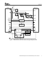
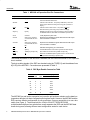
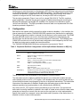
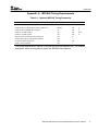
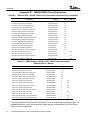
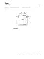
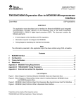
Application Report SPRA540B - August 2001 TMS320C6000 Expansion Bus to MPC860 Microprocessor Interface Zoran Nikolic DSP Applications ABSTRACT This application report describes how to interface the TMS320C6000 (C6000) digital signal processor (DSP) expansion bus to the Motorola MPC860 microprocessor. This document contains: • A block diagram of the interface and PAL equations • Information required for configuring the MPC680 • Timing diagrams illustrating the interface functionality Note: The information presented in this application report has been verified using VHDL simulation. Contents 1 MPC860 Interface . . . . . . . . . . . . . . . . . . . . . . . . . . . . . . . . . . . . . . . . . . . . . . . . . . . . . . . . . . . . . . . . . . . . 2 2 Configuration . . . . . . . . . . . . . . . . . . . . . . . . . . . . . . . . . . . . . . . . . . . . . . . . . . . . . . . . . . . . . . . . . . . . . . . 5 3 Timing Verification . . . . . . . . . . . . . . . . . . . . . . . . . . . . . . . . . . . . . . . . . . . . . . . . . . . . . . . . . . . . . . . . . . . 6 4 References . . . . . . . . . . . . . . . . . . . . . . . . . . . . . . . . . . . . . . . . . . . . . . . . . . . . . . . . . . . . . . . . . . . . . . . . . 10 Appendix A MPC860 Timing Requirements . . . . . . . . . . . . . . . . . . . . . . . . . . . . . . . . . . . . . . . . . . . . . . 11 Appendix B TMS320C6000 Timing Parameters . . . . . . . . . . . . . . . . . . . . . . . . . . . . . . . . . . . . . . . . . . . 12 Appendix C PAL Equations . . . . . . . . . . . . . . . . . . . . . . . . . . . . . . . . . . . . . . . . . . . . . . . . . . . . . . . . . . . . . 13 List of Figures Figure 1. TMS320C6202 to MPC860 Interface Using the Expansion Bus . . . . . . . . . . . . . . . . . . . . . . . . . 3 Figure 2. Burst Read by an External Master (MPC860) From Expansion Bus Synchronous Host Port . . . . . . . . . . . . . . . . . . . . . . . . . . . . . . . . . . . . . . . . . . . . . . . . . . . . . . . . 7 Figure 3. Burst Write by an External Master (MPC860) From Expansion Bus Synchronous Host Port . . . . . . . . . . . . . . . . . . . . . . . . . . . . . . . . . . . . . . . . . . . . . . . . . . . . . . . . 8 List of Tables Table 1. MPC860 to Expansion Bus Pin Connections . . . . . . . . . . . . . . . . . . . . . . . . . . . . . . . . . . . . . . . . . . 4 TMS320C6000 and C6000 are trademarks of Texas Instruments. Trademarks are the property of their respective owners. 1 SPRA540B Table 2. DSP Byte-Enable Conversion Table . . . . . . . . . . . . . . . . . . . . . . . . . . . . . . . . . . . . . . . . . . . . . . . . . 4 Table 3. Expansion Bus Boot Configuration via Pull-Up/Pull-Down Resistors on XD[31:0] . . . . . . . . . . 5 Table 4. Timing Requirements for TMS320C6000 (MPC860 Expansion Bus Master) . . . . . . . . . . . . . . . 9 Table 5. Timing Requirements for MPC860 (MPC860 Expansion Bus Master) . . . . . . . . . . . . . . . . . . . . 9 Table A–1. Motorola MPC860 Timing Parameters . . . . . . . . . . . . . . . . . . . . . . . . . . . . . . . . . . . . . . . . . . . . 11 Table B–1. TMS320C6202, C6202B, C6204 Timing Parameters (External Device is a Master) . . . . . 12 Table B–2. TMS320C6202, C6202B, C6203, C6204 Timing Parameters (TMS320C620x is a Master) . . . . . . . . . . . . . . . . . . . . . . . . . . . . . . . . . . . . . . . . . . . . . . . . . . . 12 1 MPC860 Interface The MPC860 integrates an embedded PowerPC core with a communications processor module (CPM) that uses a specialized RISC processor for communications. This two-processor architecture is more efficient than traditional architectures because the CPM offloads peripheral tasks from the embedded PowerPC core. Figure 1 illustrates the interface between the TMS320C6202 in synchronous host port mode and the MPC860. Note that the C6202 internal expansion bus arbiter is enabled. Although the C6202 is a slave in the following diagram, it still has the ability to arbitrate for the bus in order to use the asynchronous I/O port or FIFO interface of the expansion bus. If only these two devices share the bus, the internal arbiter of the MPC860 can be used. Although the C6202 device is used to illustrate the interface, the configuration for the C6202B, C6203, and C6204 devices should be similar. Table 1 lists the MPC860 to expansion bus pin connections. 2 TMS320C6000 Expansion Bus to MPC860 Microprocessor Interface SPRA540B +Vcc MPC860 TMS320C6202 BR BB D XHOLD Q BG D D Q D Q Q D XHOLDA Q CLKOUT XCLKIN TSIZE[1:0] Byte Enable Conversion A[31:30] 4 RD/WR TS XBE[3:0] XW/R XAS Address Decoder A[0:28] XCS XCNTL XRDY XBLAST A[29] TA BDIP 32 32 D[0:31] 1B 2X HRESET XBUS Boot Configuration SN74CBT16390 XD[31:0] RESET 32 2B Optional OE1 MPC860 Boot Configuration OE2 Reset Figure 1. TMS320C6202 to MPC860 Interface Using the Expansion Bus TMS320C6000 Expansion Bus to MPC860 Microprocessor Interface 3 SPRA540B Table 1. MPC860 to Expansion Bus Pin Connections Expansion Bus Pin MPC860 Pin Comments XCNTL A[29] Address bits of MPC860 are used as control signals. A31 is the LSB of the MPC860 address bus. XBLAST BDIP Indicates a burst transfer. The polarity of XBLAST (in this case active high) is determined during reset using pull-up resistor on XD[13]. XW/R RD/WR Indicates a read or write access. The polarity of XW/R is determined during reset using pull-up resistor on XD[12]. XD[31:0] D[0:31] MPC860 uses D[0:31] for 32-bit port interface. D0 is the MSB of the MPC860 data bus, while XD31 is the MSB of expansion bus. XCLK CLKOUT Local (Expansion) bus clock XHOLD Glue logic is needed to connect to BR, BG, and BB. Expansion bus arbitration signals. Note that internal expansion bus Arbiter is enabled. XHOLDA Glue logic is needed to connect to BR, BG, and BB. Expansion bus arbitration signals. Note that internal expansion bus arbiter is enabled. XAS TS Indicates the beginning of a new transfer XCS A[28:0] The MPC860 address is decoded to generate the XCS\ signals. XBE[3:0] TSIZE[1:0] and A[31:30] Byte enables are decoded using TSIZE and A[31:30] XRDY TA SETA bit in the MPC860 option register is set to 1 to indicate that TA is generated externally by expansion bus. The internal bus arbiter of the MPC860 is disabled and the internal bus arbiter of the expansion bus is enabled. The byte enables signals of the DSP are decoded using the TSIZE[1:0] and the address lines A[31:30] of the MPC860. Conversions are presented in Table 2. Table 2. DSP Byte-Enable Conversion Table TSIZE Address XBE[3:0] A30 A31 01 0 0 0111 01 0 1 1011 01 1 0 1101 01 1 1 1110 10 0 0 0011 10 1 0 1100 00 0 0 0000 The MPC860 (as well as the expansion bus) uses the pull-up/down resistors on the data bus (expansion data bus) for boot configuration during hard reset. However, the MPC860 and the DSP require a different configuration of pull-up resistors. One way around this is to use a bus switch (see Figure 1). The bus switch (two 16-bit to 32-bit FET SN74CBT16390 multiplexer/demultiplexer bus switches are used) separates the DSP and the MPC860 data buses during reset, allowing different reset configuration words for each device. 4 TMS320C6000 Expansion Bus to MPC860 Microprocessor Interface SPRA540B Another way to reset the system is to first bring the MPC860 from hard reset (pull-up/pull-downs on the XBUS are used to configure the MPC860 during reset). The DSP should come out from reset after the MPC860. During reset of the DSP, the MPC860 should actively drive values required to configure the DSP on the data bus; this way the DSP will be configured. The glue logic presented in Figure 1 can not fit in a single PALLV22V10. The PAL equations given in Appendix C describe only the glue required for address decoding and converting the MPC860 bus arbitration signals (BR, BG, and BB) to the expansion bus arbitration signals (XHOLD and XHOLDA). The DSP byte-enable conversion table is not implemented in the PAL equations provided in Appendix C. 2 Configuration Both devices can operate with the internal bus arbiter enabled or disabled. In this interface, the internal expansion bus arbiter (TMS320C6000 DSP expansion bus) handles the bus arbitration. The arbiter configuration (external or internal) for both devices is set at system reset. The ERAB bit of the MPC860 must be set to one in the hard reset configuration word sampled by the MPC860 from the data bus during reset (external arbitration is assumed). The XARB bit of the C6000 DSP must be set to one in the hard reset configuration word sampled by the DSP from the data bus during reset to enable the internal bus arbiter. The TMS320C6202(B)/C6203/C6204 boot configuration is presented in Table 3. Table 3. Expansion Bus Boot Configuration via Pull-Up/Pull-Down Resistors on XD[31:0] Field Description BLPOL Determines polarity of /XBLAST signal BLPOL = 1, XBLAST is active high. RWPOL Determines polarity of expansion bus read/write signal RWPOL = 1, XR/W_ HMOD Host mode (status in XB HPIC) HMOD = 1, external host interface is in synchronous master/slave Mode. XARB Expansion bus arbiter (status in XBGC) XARB = 1, internal expansion bus arbiter is enabled. FMOD FIFO mode (status in XBGC) LEND Little-endian mode LEND = 1, system operates in little-endian mode. BootMode[4:0] Dictates the boot mode of the device, including host port boot, ROM boot, memory map selection. For a complete list of boot modes, see the TMS320C6000 Peripherals Reference Guide (SPRU 190). The MPC860 cache must be disabled for the interface to function correctly. The data cache may be enabled or disabled through the use of data cache enable and data cache disable written to the DC_CST register. In the disabled state, the cache tag state bits are ignored and all accesses are propagated to the bus as single beat transactions. The default after reset state of the data cache is disabled. Disabling the data cache does not affect the data address translation logic and translation is still controlled by the MSRDR bit. Any write to the DC_CST register must be preceded by a sync instruction. This prevents the data cache from being disabled or enabled in the middle of a data access. When the data cache generates an interrupt as a result of the bus error on the copy-back or on the implementation specific flush cache line command, it enters the disable state. Operation of the cache when it is disabled is similar to cache-inhibit operation. TMS320C6000 Expansion Bus to MPC860 Microprocessor Interface 5 SPRA540B Each page can have different storage control attributes. The MPC860 supports cache inhibit (CI), write-through (WT), and guarded (G) attributes but not the memory coherence (M) attribute. A page that must be memory coherent must be programmed cache-inhibited. The G attribute is used to map I/O devices that are sensitive to speculative accesses. An attempt to access a page marked guarded (G bit asserted) forces the access to stall until either the access is non-speculative or is canceled by the core. Cacheable and non-cacheable regions must be defined and write-back or write-through mode for the cacheable region of main memory must be selected by initializing the MMU before enabling the data cache. 3 Timing Verification To verify proper operation, two functions have been examined: 1) an MPC860 write to the expansion bus and 2) an MPC860 read from the expansion bus. In each instance, timing requirements were compared for each of the devices and the results are shown in the following tables and timing diagrams. The interface was verified using VHDL simulation (Synopsys MPC860 SmartModel was used in the test bench). Diagrams presented are outputs from the simulation. The clock ratio between the operating frequency of the TMS320C6000 DSP and the XCLKIN frequency was set to 6.2. When the bus clocks speed is faster than 37 MHz, the MPC860 timing requirement B16 (setup time) is violated due to maximum data delay time Td(XCKIH-XRY) of the expansion bus. The numbers in Table 4 and Table 5 are based on an MPC860 (local bus is running at 36 MHz - Tcyc = 28 ns) and a TMS320C6000 DSP (the TMS320C6202 was used specifically for the simulations presented) device operating at any frequency ranging from 100 MHz-250 MHz. Note that the expansion bus timing parameters for the TMS320C6202, C6202B, C6203, and C6204 are similar for the specific frequency range. 6 TMS320C6000 Expansion Bus to MPC860 Microprocessor Interface .../xrdy .../xwnr .../xcntl .../xbe F F F 0 F .../xcs .../xhold .../xholda .../xas .../xblast .../xd .../mpc860_a FFFFFFFF 44444444 FFFFFFFF 55555555 66666666 77777777 00000008 .../mpc860_breq .../mpc860_bgnt .../mpc860_bb .../mpc860_ts .../mpc860_bdip 17900 ns Entity:chiptb Architecture:bhv 18 us 18100 ns Date: 18200 ns 18300 ns Mon Mar 15 15:04:36 1999 18400 ns 18500 ns 18600 ns Page 1 7 SPRA540B TMS320C6000 Expansion Bus to MPC860 Microprocessor Interface Figure 2. Burst Read by an External Master (MPC860) From Expansion Bus Synchronous Host Port .../xclkin Figure 3. Burst Write by an External Master (MPC860) From Expansion Bus Synchronous Host Port TMS320C6000 Expansion Bus to MPC860 Microprocessor Interface SPRA540B 8 .../xclkin .../xrdy .../xwnr .../xcntl .../xbe F F F 0 F .../xcs .../xhold .../xholda .../xas .../xblast .../xd .../mpc860_a FFFFFFFF FFFFFFFF 44444444 55555555 66666666 77777777 FFFFFFFF 00000008 FFFFFFFF .../mpc860_breq .../mpc860_bgnt .../mpc860_bb .../mpc860_ts .../mpc860_bdip 14900 ns Entity:chiptb Architecture:bhv 15 us Date: 15100 ns 15200 ns Mon Mar 15 15:07:19 1999 15300 ns Page 1 15400 ns SPRA540B Table 4. Timing Requirements for TMS320C6000 (MPC860 Expansion Bus Master) MPC860 Symbol C6000 Symbol Parameter MPC860 Min (ns) C6000* Min (ns) 10 3.5 Tcyc-B8-tPAL Tsu(XCSV-XCKIH) Chip-select (XCS) valid before XCLKIN high B12+tPAL Th(XCKIH -XCSV) Chip-select (XCS) valid after XCLKIN high 11.25 2.8 Tcyc-B11 Tsu(XASV-XCKIH) Address strobe (XAS) valid before XCLKIN high 15.75 3.5 B11 Th(XCKIH-XASV) Address strobe (XAS) valid after XCLKIN high 6.25 2.8 Tcyc-B8a Tsu(XBLTV-XCKIH) Burst last (XBLAST) valid before XCLKIN high 15 3.5 B8a Th(XCKIH-XBLTV) Burst last (XBLAST) valid after XCLKIN high 6.25 2.8 Tcyc-B8 Tsu(XD-XCKIH) Data (XD) valid before XCLKIN high (WRITE) 15 3.5 B7 Th(XCKIH-XD) Data (XD) valid after XCLKIN high (WRITE) 6.25 2.8 Tcyc-B8-tPAL Tsu(XBEV-XCKIH) Byte Enable (XBE[3:0]) valid before XCLKIN high 10 3.5 B7+tPAL Th(XCKIH-XBEV) Byte enable (XBE[3:0]) valid after XCLKIN high 11.25 2.8 Tcyc-B8 Tsu(XWR-XCKIH) Read/write (XR/W) valid before XCLKIN high 15 3.5 B7 Th(XCKIH-XWR) Read/write (XR/W) valid after XCLKIN high 6.25 2.8 * C6000 refers to the C6202, C6202B, C6203, and C6204 devices. Table 5. Timing Requirements for MPC860 (MPC860 Expansion Bus Master) MPC860 Symbol C6000 Symbol Parameter MPC860 Min (ns) C6000* Min (ns) B16 Tcyc-Td(XCKIH-XRY) Ready signal (XRDY) valid before XCLKIN high 9.75 11.5 B17 Td(XCKIH-XRY) Ready signal (XRDY) valid after XCLKIN high 1 5 B18 Tcyc-Td(XCKIH-XDV) Data (XD) valid before XCLKN high (READ) 6 11.5 B19 Td(XCKIH-XDIV) Data (XD) invalid after XCLKIN high (READ) * C6000 refers to the C6202, C6202B, C6203, and C6204 devices. 1 5 TMS320C6000 Expansion Bus to MPC860 Microprocessor Interface 9 SPRA540B 4 References 1. 2. 3. 4. 5. 10 TMS320C6000 Peripherals Reference Guide (SPRU190). TMS320C6202, TMS320C6202B Fixed-Point Digital Signal Processors (SPRS104). TMS320C6203, TMS320C6203B Fixed-Point Digital Signal Processor (SPRS086). TMS320C6204 Fixed-Point Digital Signal Processor (SPRS152). MPC860 User’s Manual, Motorola Inc. TMS320C6000 Expansion Bus to MPC860 Microprocessor Interface SPRA540B Appendix A MPC860 Timing Requirements Table A–1. Motorola MPC860 Timing Parameters Characteristic Symbol Min (ns) Max (ns) CLKOUT to A[0:31], RD/WR-,D(0:31), BDIP invalid B7, B7a 6.25 CLKOUT to A(0:31), RD/WR-,D(0:31),DP(0:3), BDIP valid B8, B8a 6.25 13 CLKOUT to A(0:31),RD/WR-,D(0:31) High-Z B9 6.25 13 CLKOUT to TS-,BB- assertion B11 6.25 12.25 13 CLKOUT to TS-,BB- negation B12 6.25 Data, DP valid to CLKOUT rising edge (setup time) B18 6 CLKOUT Rising edge to Data, DP valid (hold time) B19 1 TA- valid to CLKOUT (setup time) B16 9.75 CLKOUT to TA- (hold time) B17 1 The timing requirements in Table A–1 are provided for quick reference only. For detailed description, notes, and restrictions, please the MPC860 User’s Manual. TMS320C6000 Expansion Bus to MPC860 Microprocessor Interface 11 SPRA540B Appendix B TMS320C6000 Timing Parameters Table B–1. TMS320C6202, C6202B, C6204 Timing Parameters (External Device is a Master) Characteristic Symbol Min (ns) Setup time, XCS valid before XCLKIN high Tsu(XCSV-XCKIH) 3.5 Hold time, XCS valid after XCLKIN high Th(XCKIH-XCSV) 2.8 Setup time, XAS valid before XCLKIN high Tsu(XASV-XCKIH) 3.5 Hold time, XAS valid after XCLKIN high Th(XCKIH-XASV) 2.8 Setup time, XCNTL valid before XCLKIN high Tsu(XCTL-XCKIH) 3.5 Hold time, XCNTL valid after XCLKIN high Th(XCKIH-XCTL) 2.8 Setup time, XWR valid before XCLKIN high Tsu(XWR-XCKIH) 3.5 Hold time, XWR valid after XCLKIN high Th(XCKIH-XWR) 2.8 Setup time, XBLAST valid before XCLKIN high Tsu(XBLTV-XCKIH) 3.5 Hold time, XBLAST valid after XCLKIN high Th(XCKIH-XBLTV) 2.8 Setup time, XBE valid before XCLKIN high Tsu(XBEV-XCKIH) 3.5 Hold time, XBE valid after XCLKIN high Th(XCKIH-XBEV) 2.8 Setup time, XD valid before XCLKIN high Tsu(XD-XCKIH) 3.5 Hold time, XD valid after XCLKIN high Th(XCKIH-XD) 2.8 Delay time, XCLKIN high to XD low impedance Td(XCKIH-XDLZ) 0 Delay time, XCLKIN high to XD valid Td(XCKIH-XDV) Delay time, XCLKIN high to XD invalid Td(XCKIH-XDIV) Delay time, XCLKIN high XD high impedance Td(XCKIH-XDHZ) Delay time, XCLKIN high to XRDY valid Td(XCKIH-XRY) Max (ns) 16.5 5 4P 5 16.5 Table B–2. TMS320C6202, C6202B, C6203, C6204 Timing Parameters (TMS320C620x is a Master) Characteristic Symbol Min (ns) Setup time, XD valid before XCLKIN high Tsu(XDV-XCKIH) 3.5 Hold time, XD valid after XCLKIN high Th(XCKIH-XDV) 2.8 Setup time, XRDY valid before XCLKIN high Tsu(XRY-XCKIH) 3.5 Hold time, XRDY valid after XCLKIN high Th(XCKIH-XRY) 2.8 Setup time, XBOFF valid before XCLKIN high Tsu(XBFF-XCKIH) 3.5 Hold time, XBOFF valid after XCLKIN high Th(XCKIH-XBFF) 2.8 Max (ns) Delay time, XCLKIN high to XAS valid Td(XCKIH-XAS) 5 16.5 Delay time, XCLKIN high to XWR valid Td(XCKIH-XWR) 5 16.5 Delay time, XCLKIN high to XBLAST valid Td(XCKIH-XBLTV) 5 16.5 16.5 Delay time, XCLKIN high to XBE valid Td(XCKIH-XBEV) 5 Delay time, XCLKIN high to XD low impedance Td(XCKIH-XDLZ) 0 Delay time, XCLKIN high to XD valid Td(XCKIH-XDV) Delay time, XCLKIN high to XD invalid Td(XCKIH-XDIV) Delay time, XCLKIN high to XD high impedance Td(XCKIH-XDHZ) Delay time, XCLKIN high to XWE/XWAIT valid Td(XCKIH-XWTV) 16.5 5 4P 5 16.5 The timing requirements in Table B–1 and Table B–2 are provided for quick reference only. For detailed description, notes, and restrictions, please see the corresponding Fixed-Point Digital Signal Processor data sheet. 12 TMS320C6000 Expansion Bus to MPC860 Microprocessor Interface SPRA540B Appendix C Synario 3.10 – Device Utilization Chart PAL Equations Page 1 Fri Apr 09 15:19:35 1999 xbus860.bls –––––––––––––––––––––––––––––––––––––––––––––––––––––––––––––––––––––––––––––––– Module : ’xbus860’ –––––––––––––––––––––––––––––––––––––––––––––––––––––––––––––––––––––––––––––––– Input files: ABEL PLA file Device library : xbus860.tt3 : P22V10C.dev Output files: Report file : xbus860.rep Programmer load file : xbus860.jed –––––––––––––––––––––––––––––––––––––––––––––––––––––––––––––––––––––––––––––––– TMS320C6000 Expansion Bus to MPC860 Microprocessor Interface 13 SPRA540B Synario 3.10 – Device Utilization Chart Page 2 Fri Apr 09 15:19:35 1999 xbus860.bls P22V10C Programmed Logic: –––––––––––––––––––––––––––––––––––––––––––––––––––––––––––––––––––––––––––––––– BGn = !( N_7.Q & !N_3.Q ); XCSn = ( !TSn & !A2 & !A1 & A0 ); N_15.D N_15.C = ( = ( BBn & BRn ); ” ISTYPE ’BUFFER’ XCLIKIN ); N_11.D N_11.C = ( = ( XHOLDA ); ” ISTYPE ’BUFFER’ XCLIKIN ); N_3.D N_3.C = ( = ( N_11.Q & N_5.Q ); ” ISTYPE ’BUFFER’ XCLIKIN ); N_5.D N_5.C = ( = ( N_11.Q & N_7.Q ); ” ISTYPE ’BUFFER’ XCLIKIN ); N_7.D N_7.C = ( = ( N_11.Q ); ” ISTYPE ’BUFFER’ XCLIKIN ); XHOLD 14 = ( !N_15.Q ); TMS320C6000 Expansion Bus to MPC860 Microprocessor Interface SPRA540B Synario 3.10 – Page 3 Fri Apr 09 15:19:35 1999 Device Utilization Chart xbus860.bls XCLKIN 3 2 N5 BBn 4 XHOLD BRn P22V10C Chip Diagram: –––––––––––––––––––––––––––––––––––––––––––––––––––––––––––––––––––––––––––––––– 1 28 27 26 TSn 5 25 N11 A2 6 24 XCSn A1 7 23 P22V10C 8 XHOLDA A0 22 9 21 10 20 !BGn 11 19 N15 12 13 14 15 16 17 18 SIGNATURE: N/A TMS320C6000 Expansion Bus to MPC860 Microprocessor Interface 15 SPRA540B Synario 3.10 – Device Utilization Chart Page 4 Fri Apr 09 15:19:35 1999 xbus860.bls P22V10C Resource Allocations: –––––––––––––––––––––––––––––––––––––––––––––––––––––––––––––––––––––––––––––––– Device | Resource | Design | Resources | Available | Requirement | Unused ======================|===========|=============|============== | | | Input Pins: | | | | | | Input: | 12 | 8 | 4 ( 33 %) | | | Output Pins: | | | | | | In/Out: | 10 | 8 | 2 ( 20 %) Output: | – | – | – | | | Buried Nodes: | | | | | | Input Reg: | – | – | – Pin Reg: | 10 | 5 | 5 ( 50 %) Buried Reg: | – | – | – 16 TMS320C6000 Expansion Bus to MPC860 Microprocessor Interface SPRA540B Page 5 Synario 3.10 – Device Utilization Chart Fri Apr 09 15:19:36 1999 xbus860.bls P22V10C Product Terms Distribution: –––––––––––––––––––––––––––––––––––––––––––––––––––––––––––––––––––––––––––––––– Signal | Pin | Terms | Terms | Terms Name | Assigned | Used | Max | Unused =========================================|==========|=======|=======|======= BGn | 20 | 1 | 14 | 13 XCSn | 24 | 1 | 14 | 13 N_15.D | 19 | 1 | 12 | 11 N_11.D | 25 | 1 | 12 | 11 N_3.D | 18 | 1 | 10 | 9 N_5.D | 26 | 1 | 10 | 9 N_7.D | 17 | 1 | 8 | 7 XHOLD | 27 | 1 | 8 | 7 ==== List of Inputs/Feedbacks ==== Signal Name | Pin | Pin Type =========================================|==========|========= XCLIKIN | 2 | CLK/IN BBn | 3 | INPUT BRn | 4 | INPUT TSn | 5 | INPUT A2 | 6 | INPUT A1 | 7 | INPUT XHOLDA | 9 | INPUT A0 | 10 | INPUT TMS320C6000 Expansion Bus to MPC860 Microprocessor Interface 17 SPRA540B Synario 3.10 – Device Utilization Chart Page 6 Fri Apr 09 15:19:36 1999 xbus860.bls P22V10C Unused Resources: –––––––––––––––––––––––––––––––––––––––––––––––––––––––––––––––––––––––––––––––– Pin | Pin | Product | Flip–flop Number | Type | Terms | Type =======|========|=============|========== 11 | INPUT | – | – 12 | INPUT | – | – 13 | INPUT | – | – 16 | INPUT | – | – 21 | BIDIR | NORMAL 16 | D 23 | BIDIR | NORMAL 16 | D 18 TMS320C6000 Expansion Bus to MPC860 Microprocessor Interface SPRA540B Synario 3.10 – Page 7 Fri Apr 09 15:19:36 1999 Device Utilization Chart xbus860.bls P22V10C Fuse Map: –––––––––––––––––––––––––––––––––––––––––––––––––––––––––––––––––––––––––––––––– 44: 88: 440: 484: 924: 968: 1496: 1540: 3652: 3696: 4312: 4356: 4884: 4928: 5368: 5412: 0 –––––––––– –––––––––– –––––––––– –––––––––– –––––––––– –––––––––– –––––––––– –––––––––– –––––––––– –––––––––– –––––––––– ––––X–––X– –––––––––– –––––––X–– –––––––––– –––––––––– 0 10 –––––––––– –––––––––– –––––––––– –X–––––––– –––––––––– –––––––––– –––––––––– –––X–––X–– –––––––––– –––––––––– –––––––––– –––––––––– –––––––––– –X–––––––– –––––––––– –X–––––––– 10 20 –––––––––– –––––––––– –––––––––– –––––––––– –––––––––– ––––X––––– –––––––––– –X––––––X– –––––––––– –––––––––– –––––––––– –––––––––– –––––––––– –––––––––– –––––––––– –––––––––– 30 –––––––––– X––––––––– –––––––––– –––––––––X –––––––––– –––––––––– –––––––––– –––––––––– –––––––––– ––––X––––X –––––––––– –––––––––– –––––––––– –––––––––– –––––––––– –––––––––– 40 –––– –––– –––– –––– –––– –––– –––– –––– –––– –––– –––– –––– –––– –––– –––– –––– 5808: –––X–X––XX XXX––X–X–X TMS320C6000 Expansion Bus to MPC860 Microprocessor Interface 19 IMPORTANT NOTICE Texas Instruments and its subsidiaries (TI) reserve the right to make changes to their products or to discontinue any product or service without notice, and advise customers to obtain the latest version of relevant information to verify, before placing orders, that information being relied on is current and complete. All products are sold subject to the terms and conditions of sale supplied at the time of order acknowledgment, including those pertaining to warranty, patent infringement, and limitation of liability. TI warrants performance of its products to the specifications applicable at the time of sale in accordance with TI’s standard warranty. Testing and other quality control techniques are utilized to the extent TI deems necessary to support this warranty. Specific testing of all parameters of each device is not necessarily performed, except those mandated by government requirements. Customers are responsible for their applications using TI components. In order to minimize risks associated with the customer’s applications, adequate design and operating safeguards must be provided by the customer to minimize inherent or procedural hazards. TI assumes no liability for applications assistance or customer product design. TI does not warrant or represent that any license, either express or implied, is granted under any patent right, copyright, mask work right, or other intellectual property right of TI covering or relating to any combination, machine, or process in which such products or services might be or are used. TI’s publication of information regarding any third party’s products or services does not constitute TI’s approval, license, warranty or endorsement thereof. Reproduction of information in TI data books or data sheets is permissible only if reproduction is without alteration and is accompanied by all associated warranties, conditions, limitations and notices. Representation or reproduction of this information with alteration voids all warranties provided for an associated TI product or service, is an unfair and deceptive business practice, and TI is not responsible nor liable for any such use. Resale of TI’s products or services with statements different from or beyond the parameters stated by TI for that product or service voids all express and any implied warranties for the associated TI product or service, is an unfair and deceptive business practice, and TI is not responsible nor liable for any such use. Also see: Standard Terms and Conditions of Sale for Semiconductor Products. www.ti.com/sc/docs/stdterms.htm Mailing Address: Texas Instruments Post Office Box 655303 Dallas, Texas 75265 Copyright 2001, Texas Instruments Incorporated