Download 
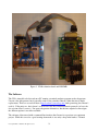
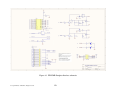
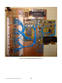
The KE0FF HC11 Programmer Interface

Transcript
The KE0FF 68HC711 PGMR Interface
By Joseph Haas, KEØFF
12/20/2013
The Motorola (now Freescale) 68HC11 processor was a workhorse in my repertoire for many years. It
features a robust peripheral compliment, along with on-board EEPROM and EPROM memory. As of
this writing, it appears that only the 711E20 parts are still available on the white market, but are in “Not
Recommended For New Design” status. The HC11 was a powerful and versatile microcontroller for its
time, but it has been supplanted by faster processors using FLASH memory that have an equal or better
compliment of peripherals, and much larger memory arrays. Still, I have several products using E9 and
D3 versions of this family, and I have a modest number of them to work with.
The HC11 features a couple of special bootstrap modes that allow the part to download short test
programs via the on-board asynchronous serial peripheral. Motorola provided free software and lowcost hardware solutions to allow for small-scale programming of the EPROM and EEPROM memories.
Unfortunately, the software solutions were written in the 80’s and maintained into the 90’s, but not
much beyond that. These DOS-era tools eventually succumbed to migration death as the PC operating
systems evolved beyond DOS compatibility. If you have an old computer, you could still run the
programs (PROG11 and PROG11D3), but keeping an old computer around and keeping it in good
working order becomes a great chore especially considering that it is only used infrequently for a single
purpose.
This project is targeted at bridging the gap between the old programmer tools and the newer computer
platforms so that I can continue to support my old 68HC11 designs without depending on a single, very
old computer. Since the application is relatively straightforward, it would make sense to simply write a
new PC application. However, I chose a microcontroller solution for two reasons: 1) It is what I know –
I have very little experience with PC application development and no development tools for that
purpose. 2) While most of the programming control takes place over a serial port, it is helpful to have
some digital control lines to drive power supply controls and the target Device Under Test (DUT) reset
input. Parallel ports are an option for these signals, but they are becoming increasingly difficult to find
as standard equipment on PCs, and USB alternatives are also rather rare and buggy. It made sense to
have an intermediate microcontroller that could provide these digital controls.
The Hardware
Since SiLabs is my latest processor of choice, I looked to their offering to see if I could find a suitable
candidate. Two serial ports and provision for expanded RAM were first on the list. Next was FLASH
capacity. From the outset, this application was intended to be a Command Line Interface (CLI) via a
terminal program running on the PC, so it was going to be very plain-text-intensive which helps eat up
processor memory. The F34x series has several parts with dual UARTs. Some of these parts also
support an external memory interface which allows for the addition of the RAM needed to hold the
programming data. They are in a small (48TQFP) package and were well under $10 each. I settled on
the C8051F34C since it had the fewest peripherals (meaning lower cost).
I managed to layout a small circuit board, but tabled that process just as it was completed due to budget
constraints. Luckily, I had an evaluation board for the F340 processor which was sufficient for the task
© Joseph M. Haas, 12/20/2013, all rights reserved
1
at hand. It has more analog peripherals than the F34C, but that didn’t impact this design. I was able to
re-purpose an existing daughter board and attach the 32K RAM, reset driver, and serial level translators.
This choice was bittersweet: on the one hand, there was very little cost involved since most of the parts
were in-hand. However, the circuit board layout was segmented with an eye towards other prototype
projects. Having a few copies on hand would mean that future projects would have the opportunity to
be quickly and neatly deployed.
I decided to run the target serial data as TTL level signals since the 7812.5 baud rate used by the HC11
is fairly low and the wire length is very short. The F340 inputs are 5V tolerant, but the serial output had
to be passed through a 74HCT device to bring it to the 5V levels needed by the HC11 DUT. This
allowed the serial connection to the DUT to be accomplished without the need for an RS-232 level
translator.
I considered making a new programming socket interface, but the offering for 52PLCC low-force
sockets has become quite limited, with the only ones I could find priced at over $200. So, for the
moment at least, I am relegated to using my old 68HC711E9PGMR and D3PGMR boards. Each was
modified to bring the serial TTL connections to unused DB-25 pins, along with 5V power, reset, and
DUT power control signals.
See Figure A1 for a schematic of the interface circuits. Target reset is driven by a simple NPN switch
while the Vdd_sw and Vpp_sw signals are driven by a modified push-pull FET switch. This switch
arrangement provides a low-resistance path between the regulators and the DUT when on, and a
medium-resistance path to GND when off. This allows the circuit to quickly discharge any bulk
capacitance on the PGMR board when in the off state, but not present an unnecessary load when in the
on state.
Figure 1 illustrates the typical assembly. Power is applied to the E9PGMR (or the D3PGMR, not
pictured) and the serial connection on the F340-DK evaluation board goes to the PC COM port (115.2
kbaud, N81, XON/XOFF handshaking enabled). My PGMR cards have been modified to provide oncard Vdd and Vpp voltage regulators. These voltages are provided to the F340 evaluation board via the
(modified) DSUB-25 connector. A single jumper on the F340-DK board brings the PGMR +5V power
from the mezzanine board the F340-DK +3.3V regulator input via an unused F340-DK header pin. This
allows the system to be powered from a single power connection to the PGMR board. The F340-DK
features a 3-position jumper for the Vin source which is removed to disable the F340-DK power
connector. This protects the 5V logic circuits and regulator from damage in case someone inadvertently
connects a power source to the F340-DK coaxial power jack. Because of the Vpp regulator
requirements, the input voltage must be at least 14.5V.
The re-purposed daughter card was embellished with a scrap of a 100TQFP protoboard that I used to
mount the 28TSSOP RAM chip. The pitch was a bit off, and there was a small gap on one side of the
RAM, but I was able to align the RAM pins without too much difficulty and apply some bare jumpers to
the other side of the 28TSSOP part to complete the connections. This provided a handy interface to the
point to point wiring that I used to connect the RAM to the processor. Another scrap of protoboard
holds the target PGMR connector (a 10 pin dual row connector) and SMD interface components. The
20 pin small-pitch ribbon connector is from a previous project and was abandoned in place.
© Joseph M. Haas, 12/20/2013, all rights reserved
2
Figure 1. F340 evaluation board and E9PGMR.
The Software
The CLI is intended to be driven from a PC running a terminal emulator program such as hyperterm.
I’m not a fan of hyperterm, but it generally works to the point that I haven’t taken the time to find a
replacement. There are several out there (http://realterm.sourceforge.net/ looks promising, but I haven’t
used it). I like putty.exe, but it doesn’t seem to have ASCII or Xmodem transfer protocols (at least, the
free version doesn’t seem to). I’m open to hyperterm alternatives, but the time required to investigate
the different options is not often available.
The software effort started with a command line interface that I wrote for a previous test equipment
project. While this served as a good starting framework, it was only a drop in the bucket. I wanted
© Joseph M. Haas, 12/20/2013, all rights reserved
3
Xmodem transfer capability, so I re-invested some time re-learning the inner workings of Xmodem so
that I could write a set of C driver-like routines for handling Xmodem transfers. I’ve performed this
task several times before, but not on a regular basis, so the details have to get re-learned each time I
deploy Xmodem anew.
So, why Xmodem? The short answer: packet size and simplicity. Ymodem, 1K Xmodem, Zmodem,
etc… all feature a 1K (or larger) packet size. This alone generally improves transfer efficiency, but with
MCU applications, memory can be scarce. For this application, scarcity isn’t too much of an issue, but I
didn’t know that going in (I have kept the 32K SRAM off-limits for system functions because it is
dedicated for device data storage). The other side of the coin is that Xmodem is relatively simple. This
has its drawbacks (hence the plethora of follow on protocols) but for a relatively noise-free channel
(such as a direct PC-MCU connection over a short run cable), these drawbacks are not generally an
issue. Two aspects of Xmodem that I really like are that the receiver regulates the data flow (within the
limits of the timeout timers) and the system can detect transfer errors AND recover from them (within
the limits of the checksum/crc and retry counters). These two subtleties make Xmodem very attractive
for device data transfers.
Once the Xmodem transfers were worked out, I started on the S-record transfer algorithms. I limited the
code to S19 transfers, since none of my assemblers can generate S28 or S37 records. Intel HEX records
are also supported if only because it was easy to do (the support is seamless, just send the data and the
software figures out what it is receiving). I also included support for S0 records by adding a feature that
I’m pretty pleased with. S0 records were originally intended to provide reference information, such as
file name, date, revision, etc… I have used them in the past to communicate bank information for
systems which utilized bank-switched program memory, which is a more limited relative of the feature
that I am building up to. The S0 feature I implemented here is a batch command interpreter. Batch
commands (bcmds) can be placed into the data field of an S0 record, and those commands can be
processed by the programmer interface during upload. This allows the device programming to be
largely automated, which greatly streamlines the process.
The supported bcmds are: PGM DUT, Verify DUT, Config register program, Blank check, BUlk erase,
Fill pgmr memory, pgmr CHecksum, address Offset, and DEvice select. These represent all of the
salient commands that might be employed to program a device (although, not all are required). This
would allow one to construct a single object file that would set the device, blank check memory,
program the CONFIG register, upload object data for EPROM and/or EEPROM, calculate and store
checksums (as many as are required), program EEPROM and/or EPROM memories, and then verify the
programmed data. The batch commands produce a cryptic but very low character count response set
that is buffered and displayed at the end of the transfer (thus, allowing for the batch feature to be used in
Xmodem transfers).
But first, I had a lot of other coding work to do. After the transfer protocols were coded and mostly
working, I turned my attention to the target processor. As mentioned earlier, the HC11 was designed to
be programmed via small test programs loaded via the serial port. There is a simple protocol for loading
the programs, but that still took several attempts to get working (even simple things can be complicated
when you don’t consider all of the subtleties involved).
© Joseph M. Haas, 12/20/2013, all rights reserved
4
The actual test programs also needed to be developed. I needed one for each function: EEPROM bulk
erase, CONFIG program, blank check, upload memory, program EEPROM, and program EPROM. I
also ended up coding a device query function that would read the contents of the bootrom identity
memory locations. This task was complicated by the fact that there are several variants of the 68HC711
(and one of the 68HC811) that I wanted to support AND I wanted one set of functions to work with all
processor variants.
All of the HC11 variants are similar, but each one has subtle differences that can complicate the
communication process. For example, most variants support a variable test program length such that
you only transfer the program data, and then the DUT will execute the program after more than 5 serial
byte times have expired. Other variants feature a fixed program transfer size. The following is a list of
the HC11 microcontroller variants (and whether the download is fixed or variable) supported by this
project:
MC68HC811E2 (fixed)
MC68HC711D3 (var)
MC68HC711E9 (var)
MC68HC711E20 (var)
MC68HC711E32 (var)
Additionally, there are several other devices that are also supported under the E9 device, such as the E0,
E1, and E2. However, these devices generally have limited or no internal memory.
Some of the devices (such as the HC811E2) have a fixed program size which is longer than the shortest
maximum program size allowed by variants such as the HC711D3. Also, most devices have the
peripheral registers located at address $1000 except for the HC711D3, which has the registers located at
address $0000. This particular difference further complicates matters in that the start of RAM, which is
normally at address $0000, is at address $0040 for the 711D3. All of these differences make it more
difficult to produce a single set of HC11 target functions to operate on all of the desired HC11 variants.
I was determined to keep the target functions the same for all of the HC11 variants. This would save
FLASH memory on the F34x processor and simplify the management of the target functions. I was able
to get around the D3 variant issues by making the object code run-time relocate-able so that the start,
end, and register address values that are transferred as part of the HC11 function code can be accessed
by the HC11 function. These values are “tacked” on to the end of the test code during the load process
which means that their addresses can be predicted only if the start address of the function is known. I
employed a novel technique for determining the start of code address, and then used this address to selfmodify the code to point to the desired memory locations. Generally, this is a dangerous practice, but in
this case, the application scope is very narrow and there are no other competing resources (such as
interrupts or other applications), so it was deemed an acceptable risk.
This took care of most of the issues, except for the device query code. This code needed to work for all
of the variants without knowing which one beforehand, since it was intended to verify the device that the
operator had selected (which could be wrong). The solution here was to assign a fixed length of 256
bytes (the length of the only fixed program-size device supported here) to the device interrogate function
transfer. This didn’t impact the devices that had a variable length at or greater than the 256 byte size.
For the shorter variable-length parts, the code was written such that it would continue to receive (and
return) data values until they stopped, after which, the code sends back the ROM readings. These
© Joseph M. Haas, 12/20/2013, all rights reserved
5
exceptions allowed a single set of HC11 test functions to be created that would work across all
supported HC11 devices.
Most of the code development followed the very informal specs I had neatly tucked away inside my
head, but there was some feature creep (as always). For example, the original list of batch commands
that were to be supported was much shorter. It was expanded after I started testing the batch commands
and began seriously considering how I would be using them in practice. Next, a couple of utilities to
allow the S0 batch commands to be generated and read (after embedding into an object file) to simplify
the process of creating the embedded batch commands, and maintaining them down the road (the data
field of an S-record is not generally human-readable). I added a memory read/modify command to
allow direct editing of the programmer memory – This was included to aid in system test during
development, but also provides limited object code edit access to support on-the fly code or data tweaks,
so I left the command in place.
Another creep was to add XON/XOFF handshaking. Originally, this was not envisioned since the
UART driver was interrupt driven and buffered. This along with the fact that the F34x is running at
48MHz meant that it should be able to keep up even at 115.2 kbaud. However, the bcmds that involve
programming and HC11 command operations introduce a considerable delay. The HC11 EEPROM
takes 10 ms to program a byte. HC11 EPROM is faster at around 3 ms, but even this is very slow
compared to the data that can be transferred at 115.2 kbaud. Also, HC11 commands are transferred at
7812.5 baud, which means that it takes about 64ms to send a 50-byte command function to the target
(plus another 100ms to toggle the target reset signal). All of these various delays meant that
handshaking was required to keep the host from over-running the programming interface.
During Xmodem transfers, the system is able to hold off the host by simply delaying the end of packet
AKN response. However, during ASCII transfers, one must use handshaking. Since the other phases of
the interface operation did not require handshaking, the F34x software only uses XON/XOFF during
upload procedures when the host is sending S-record data. An XOFF is sent at the end of the S-record
line and an XON is sent when the S-line processing has finished. For S1 data lines, this introduces
about 95us of delay (@115.2 kbaud) to each S-line transferred. For a typical transfer involving the
entire EPROM of an E9 part (12,288 object bytes) this would add a total of only about 72ms of time to
the transfer (well beyond the ability of a human operator to perceive, especially over the several seconds
that it takes to complete a transfer). XON/XOFF is disabled during Xmodem transfers.
Finally, I added an auto-baud-rate detection feature to allow other baud rates to be easily supported. The
feature depends on a specific user interaction that is only available after reset of the SiLabs processor.
Upon reset, the SiLabs processor initializes to 115.2 kb and sends the software version message. If a
carriage return (ASCII 0x0D) is issued from the host terminal at one of the supported baud rates (115.2,
57.6, 38.4, 19.2, or 9.6 kbaud), the processor will adjust to the new baud rate and lock-out further
changes (in the case of 115.2 kb, there is no adjustment, just lock-out). Once changes are locked-out,
the baud rate cannot be changed until the SiLabs processor is reset. This feature provides the flexibility
to support systems that do not have, or cannot reliably support, the faster baud rates.
© Joseph M. Haas, 12/20/2013, all rights reserved
6
Software Design Data
The project design including source code is contained within a zip archive available at
www.rollanet.org/~joeh/projects/archives/pgmr11.zip. The archive contains several folders, one of
which holds the Keil C project for the SiLabs C8051F340-DK evaluation board with memory and I/O
added. Another folder holds the assembly files for the HC11 target functions. Each HC11 assembly file
is stand-alone and does not require any include files. They were assembled using ASM11 from
ASPiSYS (www.aspisys.com/asm11.htm). A pair of batch files were employed to simplify the DOS
command line formatting and, additionally, a set of PERL scripts were written to convert the S-record
object code output to C-formatted arrays that could be included in the C code. The combination of batch
and PERL files allowed turnkey processing of ASM source files to C source files. This greatly
simplified the development process and makes it easy to maintain the system should changes be
implemented later. There is a perl_readme.txt file that describes how to obtain and use the PERL
interpreter. I’ve installed it twice and it is a relatively quick and painless endeavor.
Keil now offers a free license for the SiLabs 8 bit MCUs. It is unlimited in object size but works only
for the SiLabs 8-bit processors. Consult www.silabs.com and www.keil.com for more information
regarding their development tools.
The software is modularized into the following components/files:
main.c
initdevice.c
serial.c
srec.c
cmd_fn.c
version.c
typedef.h
power-on reset initialization, main polling loop, application timer interrupt
holds output from SiLabs ConfigWizard for processor initialization
serial I/O drivers and Xmodem drivers
S19 record I/O drivers
command-line-interface command functions and low-level subroutines
SW version and date
holds #define type definitions that are bit-size-centric. i.e., U8 is an unsigned byte
(unsigned char), S16 is a 16 bit signed type (int), etc… If you are trying to compile
this design on another processor, especially one that is 16-bit or larger, you may have
to spend some time in this header file to optimize the type defines.
In addition, there are several files titled “hc11_xxx.c” where “xxx” is the HC11 function name. These
files hold the object code for the corresponding HC11 function and also a C-function to return the size of
the function-code array. The length is important because the function code can not be characterterminated since all character values are valid object bytes. “hc11_fns.h” applies to all of the HC11
object includes. “hc11_fns_blank.h” is used by the PERL scripts as the kernel to generate the
“hc11_fns.h” file. Thus, this file is not directly compiled, but is needed by the PERL scripts as the basis
for the finished header file.
I have used the Raisonance compiler a few times and this has taught me that there are, in fact,
differences from one compiler suite to the next. The Keil standard libraries use “char” types for many of
the STDIO function return values. “int” is more typical and the Raisonance compiler complains about
this when trying to port Keil source to Raisonance. Additionally, the Rasionance compiler offers up
complaints about the interrupts and some functions requiring the deployment of a pragma to ensure that
the registers are properly handled during interrupt processing. I have a reasonable understanding of the
© Joseph M. Haas, 12/20/2013, all rights reserved
7
issue, but am unclear as to why the Keil tool doesn’t offer this complaint (and seems to work without
issue). I’ve not seen any configuration item that seems to correlate to the register handling for interrupts
and functions in the Keil tool and have not yet had the bandwidth to try to find out and answer as to why
the two tools might be different in this regard.
The F34x source is relatively free with XDATA memory – I made some effort to constrain RAM needs,
but didn’t fret over it too much. After all is said and done, there is plenty to spare. The F34C/F340 has
4K of internal XDATA and this application uses about half that. Ports of this code to other processors
should be relatively painless beyond the I/O drivers, as long as there is enough RAM available for the
functions.
Hardware Design Data
As mentioned earlier, the application-specific hardware was constructed on a mezzanine daughter card
(The schematic of which is in Appendix A). Another schematic is present in the design archive which
represents the PCB layout that is also contained in the archive. This schematic includes connectors,
power supplies for Vdd and Vpp, and the switching circuits for each. Wire jumpers are required for
many of the signals. This was done intentionally to simplify the design with an eye towards overall size
reduction, and to allow the sub-sections of the PWB to be “severable” – allowing them to be dissected
and deployed in other, as yet to be determined, projects. The jumper count is around a dozen wires,
which is rather modest considering the total number of component interconnects in the overall design.
Finally, there is a bill of materials (BOM) in “.xls” format that lists all of the soldered components on
the PCB design.
The mezzanine card featured pad-per-hole, 0.1” centers, double sided, plated-thru holes with dual row
connectors placed at the corresponding dual row port headers on the F340-DK board. A 96 pin euroDIN connector (right-angle, male) and a piece of protoboard could also be employed to equal effect.
The key hardware pieces are the 32K SRAM, the 74HCT1G08 level translator for the TXD1 output (the
“T” in “HCT” is important since this gate is operated at 5V and the “T” specifies TTL voltage levels for
the input – these levels provide more margin for 3.3V logic inputs than does a standard HC logic
device), and the NPN open-collector reset driver. The Vdd_sw and Vpp_sw circuits help streamline the
programming interface by placing the DUT socket in a swap-safe condition. However, these features
could also be provided by switches (such as are present on the E9PGMR board) for manual control.
The more difficult task in replicating this design lies in the Motorola PGMR board. If you have one that
is in good working order, you are home free. Otherwise, you are going to have to locate a 52PLCC low
or zero insertion force socket. These are likely available on the surplus market but you may need to
scrounge a bit to find one. A regular 52PLCC socket could be employed, but this option will have a
more limited useful life span due to the high volume of insert-remove cycles. A note regarding the
Motorola PGMR boards: These boards were designed to be daisy-chained to allow gang-programming
of up to 8 DUTs at a time. While the hardware as presented could accommodate this configuration, I
did not consider supporting this in the software. One would either have to reverse engineer the PROG11
software to see how this was originally accomplished, or devise a multi-programmer serial protocol
from scratch. I have neither needed nor wanted this, so it wasn’t even considered.
© Joseph M. Haas, 12/20/2013, all rights reserved
8
The PGMR board is little more than a socket and crystal. The factory-built PGMR features an RS-232
transceiver (which is bypassed for this application), a reset monitor IC, and some bypass capacitance.
Additionally, it is important to tie all of the unused HC11 inputs to ground or Vdd. I added Vpp and
+5V regulators to simplify the connection process. In truth, these regulators were added many years
ago. If I were to have built this project upon un-modified PGMR boards, it is likely that I would have
placed the voltage regulators on the mezzanine board which would limit the modifications needed to the
PGMR board. In fact, the PCB layout included in the design file contains the Vdd and Vpp power
supplies.
Conclusion
This project took about 2 linear months to complete – mostly evenings and weekends. A fair chunk of
time was devoted to the PCB layout. The early musings went back at least 12 months prior, although
there wasn’t any real design effort during this time. Overall, I am very pleased with the result. I would
like to add some verification capability to the DEvice status data so that the programmer could signal a
flag if the bootrom ID bytes don’t match the expected values. Other than that, I haven’t been able to
cook-up any new features to add (and I usually have no difficulty thinking up new features).
References
AN1060, M68HC11 Bootstrap Mode (appnote), Jim Sibigtroth (et. al), Freescale Semiconductor, Rev
1.1, July, 2005
EB422, Enhanced M68HC11 Bootstrap Mode (engineering bulletin), Steven McAslan, Freescale
Semiconductor, 2000
M68HC711E9PGMR Programmer Board User’s Manual, Motorola Semiconductor, May 1991
M68HC11E Family Data Sheet, Freescale Semiconductor, Rev 5.1, July, 2005
M68HC11 Reference Manual (M68HC11RM/D), Freescale Semiconductor, Rev 6.1, July, 2005
C8051F34x Family Data Sheet, Silicon Laboratories, Rev 1.4, September, 2009
C8051F34X Development Kit User’s Guide, Silicon Laboratories, Rev 0.2, 2006
© Joseph M. Haas, 12/20/2013, all rights reserved
9
Appendix A: Reference Data
Command Line Interface help message:
FF-PGMR11 Protocol Converter
Vers: 1.0, Date: 15-Dec-2013
FF-PGMR11 CMD List:
DEvice (dut) select
Upload/vfy host->pgmr
CHecksum object
Blank chk dut
BUlk erase EEPROM
PGM dut
Verify dut
Fill/vfy pgmr ram
dut Config reg
Download pgmr->host
COpy dut->pgmr
srec rx Offset
TEST1 run dut test
TEST2 run pgmr test
S0 bcmd parse
pgmr software VERSion
Syntax: <cmd> <arg1> <arg2> ... args are optional depending on cmd.
<arg> order is critical except for floaters.
"?" as first <arg> gives cmd help, "? ?" lists all cmd help lines. When
selectively entering <args>, use "-" for <args> that keep default value.
"=" must precede decimal values w/o spaces. Floating <args>: these non-number
<args> can appear anywhere in <arg> list: "X" = xmodem, "W" = wait for
operator, "EPROM" = eprom opr (EEPROM opr is default), "V" = verify modifier.
Note: XON/XOFF handshake required if ascii uploads are employed with bcmds.
Supports baud rates of 115.2, 57.6, 38.4, 19.2, and 9.6 kb. Press <Enter>
as first character after reset at the desired baud rate.
DEVice sel: ?/devid
Turns on DUT power (except NO DEVICE = power off) & Clears error LED.
68HC(7)11 devid: E2 (811), D3, E9, LE20, E20, E32, N (no dev).
E20 accesses 12K segment, LE20 accesses 8K segment.
Note: E9 selection will access E1, E2, and E9 parts.
COpy DUT->pgmr: ?/EPROM/start_addr/end_addr
Upload host->pgmr: ?/Xmodem/Verify/Response
Response: re-disp last bcmd responses.
Processes S0 bcmds as they are encountered during upload.
A fail of the Blank bcmd disables bcmds remaining in upload.
CHecksum: ?/S/C/start_addr/end_addr/stor_addr/initial/poly/EPROM
defaults:
DUTstart
DUTend <no store>
0
$1021
S = checksum (16b, uses init), C = crc (16b, uses init & poly).
Config: ?/reg_bits
BUlk erase DUT EEPROM: ?/
Blank check DUT: ?/start/end/EPROM
PGM pgmr->DUT: ?/EPROM/start_addr/end_addr
Download pgmr->host: ?/X/W/EPROM
TEST1 (DUT test): ?/Ram/X (loads user RAM pgm from host)
TEST2 (PGMR test): ?/ (pgmr ram test)
S0 cmd parse util: ?/U/"<bcmd> <args> .. <args>" (45 chrs max, quoted)
Valid bcmds = Fill, Pgm, Vfy, Dev, Blank, BUlk, CHks, Config, or Offs.
This command parses batch cmds (bcmds) without any error checking.
"U" un-parse: do file upload (ascii only, data ignored), displays bcmds.
Offset: ?/offset value
Signed <offset value> added to Srecord address during upload.
range is $0000 to $FFFF (or +$7FFF to -$8000 if signed numbers).
Fill/vfy pgmr ram: ?/data/start_addr/end_addr/V
'V' <arg> to verify pgmr memory data instead of fill.
pgmr Mem write: ?/addr/data
Verify DUT->pgmr: ?/EPROM/start_addr/end_addr
© Joseph M. Haas, 12/20/2013, all rights reserved
10
Example Programming Script:
S018000052454D005330005445535400534352495054000A0061
S00A000044004539000A0029
S007000042000A00AC
S00D000042004550524F4D000A0023
S00A000043003039000A003F
S007000046000A00A8
S013000046003000423630300042374646000A008F
S123FA608D0018381809180918ECA818ED7B18ECAA18ED8A18A6AC5F8F18CE000020021882
S123B600188F1F2E80FCA72F1F2E80FCE72F20FE188F1F2E80FCA72F1F2E80FCE72F20FEA0
S013000043480053002D002D0042374645000A00A6
S017000050004550524F4D00464136300046413746000A001A
S007000050000A009E
S9030000FC
The plain text of bcmds in example script (comments shown are not part of the script file):
bcmds
Comments
REM S0 TEST SCRIPT
D E9
B
B EPROM
C 09
F
F 0 B600 B7FF
CH S - - B7FE
P EPROM FA60 FA7F
P
Any non-bcmd will be ignored and can be treated as a comment
Set device = 711E9
Blank check EEPROM
Blank check EPROM
Set DUT CONFIG register = $09 (this also does a bulk erase of EEPROM)
Fill all programmer interface RAM with $FF bytes
Fill programmer interface EEPROM space with $00
Calculate checksum on EEPROM, store to EEPROM addr $B7FE
Program EPROM from address $FA60 to $FA7F
Program EEPROM
The plain text output is observed by issuing an “S0 U” command to the programmer interface command
line and then uploading the desired script file as an ASCII transfer (assuming your terminal emulator
allows you to view responses during the upload process, hyperterm does). S1 records represent data
uploaded to programmer interface. Note that the plain-text utility does not list any S1 records, only S0
records are extracted and displayed.
Note: since the Config command does a bulk EEPROM erase, it should precede any EEPROM
programming commands.
S-record downloads are set to a maximum of 32 bytes per line. Upload lengths are limited by the Srecord buffer length (currently set to 110 bytes, which translates to 50 S-record data bytes). S0 lines can
hold up to 45 data bytes (longer lines result in an error).
© Joseph M. Haas, 12/20/2013, all rights reserved
11
Figure A1. FF-PGMR Daughter Interface schematic
© Joseph M. Haas, 12/20/2013, all rights reserved
12
Figure A2. FF-PGMR Daughter Interface card
© Joseph M. Haas, 12/20/2013, all rights reserved
13