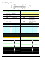
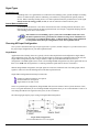
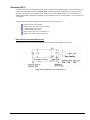
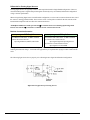
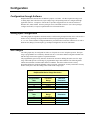
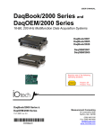
1
DaqBoard/500 Series User’s Manual
16-Bit PCI-bus Data Acquisition Boards
A Hardware Reference Manual for:
Requires one of the following
Operating Systems:
DaqBoard/500
DaqBoard/505
Windows 2000
Windows XP
IOtech, Inc.
25971 Cannon Road
Cleveland, OH 44146-1833
Phone: (440) 439-4091
Fax: (440) 439-4093
E-mail (Product Information): [email protected]
E-mail (Technical Support): [email protected]
Internet: www.iotech.com
DaqBoard/500 Series
User’s Manual
16-Bit PCI-bus
Data Acquisition Boards
p/n
1138-0901 Rev. 2.3
*324362B-01*
324362B-01
© 2006 by IOtech, Inc.
887293
ii
Warranty Information
Your IOtech warranty is as stated on the product warranty card. You may contact IOtech by phone,
fax machine, or e-mail in regard to warranty-related issues.
Phone: (440) 439-4091, fax: (440) 439-4093, e-mail: [email protected]
Limitation of Liability
IOtech, Inc. cannot be held liable for any damages resulting from the use or misuse of this product.
Copyright, Trademark, and Licensing Notice
All IOtech documentation, software, and hardware are copyright with all rights reserved. No part of this product may be
copied, reproduced or transmitted by any mechanical, photographic, electronic, or other method without IOtech’s prior
written consent. IOtech product names are trademarked; other product names, as applicable, are trademarks of their
respective holders. All supplied IOtech software (including miscellaneous support files, drivers, and sample programs)
may only be used on one installation. You may make archival backup copies.
CE Notice
Many IOtech products carry the CE marker indicating they comply with the safety and emissions standards of the
European Community. As applicable, we ship these products with a Declaration of Conformity stating which
specifications and operating conditions apply.
Warnings, Cautions, Notes, and Tips
Refer all service to qualified personnel. This caution symbol warns of possible personal injury or equipment damage
under noted conditions. Follow all safety standards of professional practice and the recommendations in this manual.
Using this equipment in ways other than described in this manual can present serious safety hazards or cause equipment
damage.
This warning symbol is used in this manual or on the equipment to warn of possible injury or death from electrical
shock under noted conditions.
This ESD caution symbol urges proper handling of equipment or components sensitive to damage from electrostatic
discharge. Proper handling guidelines include the use of grounded anti-static mats and wrist straps, ESD-protective
bags and cartons, and related procedures.
This symbol indicates the message is important, but is not of a Warning or Caution category. These notes can be of
great benefit to the user, and should be read.
In this manual, the book symbol always precedes the words “Reference Note.” This type of note identifies the location
of additional information that may prove helpful. References may be made to other chapters or other documentation.
Tips provide advice that may save time during a procedure, or help to clarify an issue. Tips may include additional
reference.
Specifications and Calibration
Specifications are subject to change without notice. Significant changes will be addressed in an addendum or revision to
the manual. As applicable, IOtech calibrates its hardware to published specifications. Periodic hardware calibration is
not covered under the warranty and must be performed by qualified personnel as specified in this manual. Improper
calibration procedures may void the warranty.
Quality Notice
IOtech has been an ISO 9001 registered firm since 1996. Prior to shipment, we thoroughly test our products and
review our documentation to assure the highest quality in all aspects. In a spirit of continuous improvement,
IOtech welcomes your suggestions.
DaqBoard/500 Series User’s Manual
iii
Your order was carefully inspected prior to shipment. When you receive your system, carefully
unpack all items from the shipping carton and check for physical signs of damage that may have
occurred during shipment. Promptly report any damage to the shipping agent and your sales
representative. Retain all shipping materials in case the unit needs returned to the factory.
CAUTION
Using this equipment in ways other than described in this manual can cause
personal injury or equipment damage. Before setting up and using your
equipment, you should read all documentation that covers your system.
Pay special attention to Warnings and Cautions.
Note:
During software installation, Adobe® PDF versions of user manuals will automatically
install onto your hard drive as a part of product support. The default location is in the
Programs group, which can be accessed from the Windows Desktop. Initial
navigation is as follows:
Start [Desktop “Start” pull-down menu]
⇒ Programs
⇒ IOtech DaqX Software
You can also access the PDF documents directly from the data acquisition CD by using
the <View PDFs> button located on the opening screen.
Refer to the PDF documentation for details regarding both hardware and software.
A copy of the Adobe Acrobat Reader® is included on your CD. The Reader provides
a means of reading and printing the PDF documents. Note that hardcopy versions of
the manuals can be ordered from the factory.
DaqBoard 500 Series.pdf p/n 1038-0901
Contains the DaqBoard/500 Series hardware-related information, including pinouts,
block diagrams, and specifications.
PDFs
DaqView.pdf
p/n 457-0909
Discusses how to install and use the DaqView “out-of-the-box” data acquisition
program.
ViewXL.pdf
p/n 457-0909
Discusses how to install and use ViewXL, an add-in which augments Microsoft Excel
with data acquisition capability.
PostAcquisition Analysis.pdf
p/n 1086-0926 and p/n 1086-0922
This pdf consists of two documents. The first discusses eZ-PostView, a post data
acquisition analysis program. The application is included free as a part of product
support. The second includes information regarding eZ-FrequencyView and eZTimeView. These two applications have more features than does eZ-PostView and are
available for purchase. They can; however, be used freely during a 30-day trial
period.
iv
989394
DaqBoard/500 Series User’s Manual
Table of Contents
DaqBoard/500 Series, Installation Guide (p/n 1138-0940)
1 – Introduction
Basic Information …… 1-1
Block Diagram …… 1-2
Board Features …… 1-3
2 – Connections and Pinouts
Overview …… 2-1
68-Pin SCSI Type III Connector …… 2-2
Signal Definitions …… 2-3
TB-100 Terminal Connector Option …… 2-6
External Connections …… 2-7
3 – Configuration
Configuration through Software …… 3-1
Analog Input Configuration …… 3-1
ADC Ranges …… 3-1
DAC Ranges …… 3-2
4 – Software and Board Operation
Overview …… 4-1
Out-of-the-Box Software ……4-1
Drivers for Third-Party, Icon Driven Software …… 4-2
DaqCOM Driver …… 4-2
Theory of Operation …… 4-3
5 – CE-Compliance
Overview …… 5-1
CE Standards and Directives …… 5-1
Safety Conditions …… 5-2
Emissions/Immunity Conditions …… 5-2
6 – Specifications
Glossary
DaqBoard/500 Series
989394
v
This page is intentionally blank.
vi
989394
DaqBoard/500 Series
DaqBoard/500 Series
Installation
This guide tells how to complete the following steps for a successful installation.
Step 1 –
Step 2 –
Step 3 –
Step 4 –
Install Software …… page 2
Install Boards in Available PCI Bus-Slots …… page 3
Configure Boards ….. page 5
Test Hardware ….. page 6
Reference Note:
After you have completed the installation you should refer to the electronic documents that
were automatically installed onto your hard drive as a part of product support. The default
location is in the Programs group, which can be accessed from the Windows Desktop.
You should keep your DaqBoard’s serial number and your DaqView/500 authorization code (if applicable)
with this document. Space is provided below for recording up to 4 board numbers and their PCI bus-slot
locations. The board serial number and board type (500 or 505) is located on the solder-side of the board.
Board Identity on “Solder-Side” of the Board
Board Type
(e.g. /500, /505)
Serial Number
PCI Bus-Slot Location
Board 1
Board 2
Board 3
Board 4
The host PC can support up to four Boards.
DaqView/500 Authorization Code ____________________________
Customers who ordered DaqView/500 can find their authorization code on the authorization
code sheet located inside the sleeve of the install CD.
Customers who did not order DaqView/500 can run a 30-day free trial version, as discussed
elsewhere in the User’s Manual.
CAUTION
Take ESD precautions (packaging, proper handling, grounded wrist strap, etc.)
Use care to avoid touching board surfaces and onboard components. Only handle boards
by their edges (or ORBs, if applicable). Ensure boards do not come into contact with
foreign elements such as oils, water, and industrial particulate.
© 2004, 2005 by IOtech, Inc.
947994
1138-0940, rev 1.1
IG-1
Reference Notes:
Each DaqBoard/500 Series plugs into a PCI bus-slot. Consult your PC owner’s manual as needed.
Reference Note: Adobe PDF versions of user manuals will
automatically install onto your hard drive as a part of
product support. The default location is in the Programs
group, which can be accessed from the Windows Desktop.
Refer to the PDF documentation for details regarding both
hardware and software. Note that hardcopy versions of the
manuals can be ordered from the factory.
Minimum System Requirements
•
•
•
•
PC system with Pentium® 3 Processor
500 MHz
128 M-byte RAM
Windows 2000 or XP Operating System
Installation, A Pictorial Overview
Step 1 – Install Software
IMPORTANT: Software must be installed before installing hardware.
1.
Remove previous version Daq drivers, if present.
You can do this through Microsoft’s Add/Remove Programs feature.
2.
Place the Data Acquisition CD into the CD-ROM drive. Wait for PC to auto-run the CD. This may
take a few moments, depending on your PC. If the CD does not auto-run, use the Desktop’s
Start/Run/Browse feature and run the Setup.exe file.
3.
After the intro-screen appears, follow the screen prompts.
Upon completing the software installation, continue with step 2, Install Boards in available
PCI Bus-slots.
IG-2
DaqBoard/500 Series Installation Guide
947994
1138-0940, rev 1.1
Step 2 – Install Boards in available PCI Bus-slots
IMPORTANT: Software must be installed before installing hardware.
CAUTION
Turn off power to, and UNPLUG the host PC and externally connected equipment prior to
removing the PC’s cover and installing the DaqBoard. Electric shock or damage to equipment
can result even under low-voltage conditions.
Take ESD precautions (packaging, proper handling, grounded wrist strap, etc.)
Use care to avoid touching board surfaces and onboard components. Only handle boards by their
edges (or ORBs, if applicable). Ensure boards do not come into contact with foreign elements such
as oils, water, and industrial particulate.
IMPORTANT: Bus Mastering DMA must be Enabled.
For a DaqBoard/500 Series board to operate properly, Bus Mastering DMA must be Enabled on
the PCI slot [for which the board is to be installed]. Prior to installation, verify that your
computer is capable of performing Bus Mastering DMA for the applicable PCI slot. Note that
some computers have BIOS settings that enable [or disable] Bus Mastering DMA. If your
computer has this BIOS option, ensure that Bus Mastering DMA is Enabled on the appropriate
PCI slot.
Refer to your PC Owner's Manual for additional information regarding your PC and enabling
Bus Mastering DMA for PCI slots.
1.
2.
3.
4.
5.
6.
Turn off power to, and UNPLUG the host PC and externally connected equipment.
Remove the PC’s cover. Refer to your PC Owner’s Manual as needed.
Choose an available PCI bus-slot.
Carefully remove the DaqBoard from its anti-static protective bag. If you have not already done so,
write down the serial number of your board at this time.
Refer to the figure at the right. Remove the screw that
secures the blank adapter plate, which is associated with the
PCI slot you will be using. Refer to your PC Owner’s
Manual if needed.
Remove the blank adapter plate.
Removing a Blank Adapter Plate
1138-0940, rev 1.1
947994
DaqBoard/500 Series Installation Guide IG-3
7.
8.
9.
10.
11.
12.
13.
Refer to the figure at the right. Align the groove in the
DaqBoard’s PCI edge-connector with the ridge of the
desired PCI slot, and with the PC’s corresponding rearpanel slot.
Push the board firmly into the PCI slot. The board will
snap into position.
Secure the board by inserting the rear-panel adapter-plate
screw.
Using the previous steps, install additional boards into
available PCI bus-slots, if applicable to your application.
Replace the computer’s cover.
Plug in all cords and cables that were removed in step 1.
Apply power to, and start up the PC.
Installing a DaqBoard/500 Series Board
Note: At this point some PCs may prompt you to insert an
installation disk. While this is rare, if you do receive such a
prompt simply place the install CD-ROM into the disk drive
and follow additional screen prompts.
IG-4
DaqBoard/500 Series Installation Guide
947994
1138-0940, rev 1.1
Step 3 – Configure Boards
DaqBoard/500 Series Boards have no jumpers or switches to set. Configuration is performed entirely
through software. Refer to the following figure and steps to complete the configuration. The numbers in
the figure correspond to the numbered steps.
1. Open the “Start” menu from the Windows desktop.
2. Select “Settings.”
3. Select “Control Panel.”
4. Double-click “Daq Configuration.” This opens the Daq Configuration window.
5. Double-click on the Device Inventory’s DaqBoard/500 Series icon. In the figure above the
DaqBoard/500 appears as “DaqBoard500_0.”
The DaqBoard’s Properties tab will appear (following figure).
Note: If the DaqBoard icon is not present, skip to the upcoming section, Using ‘Add Device.’
Accessing the DaqBoard/500 Properties Tab
6. Enter a “Device Name” in the text box, or use the default, e.g., DaqBoard500_0.
The Name is for identifying the specific DaqBoard, but actually refers to the PCI slot.
7. Verify that the “Device Type” shows the correct board, i.e., “DaqBoard/500 or
DaqBoard/505.” Other devices, if available can be viewed via the pull-down list.
8. Confirm that the DaqBoard’s text box shows a Bus #, Slot #, and Serial Number.
If this text box is empty, use its pull-down list and select the serial number that matches the
one for your board.
1138-0940, rev 1.1
947994
DaqBoard/500 Series Installation Guide IG-5
Using “Add Device”
This method is for users who have accessed the Daq
Configuration control panel applet, but have no DaqBoard/500
Series device icon.
1.
After accessing the Daq Configuration control panel applet,
click on the <Add Device> button (see figure, right). The
Select Device Type window will appear.
2.
Using the Device Type’s pull-down list, select the
applicable board. In the example at the right
DaqBoard/500 is selected.
3.
Click the <OK> button. The board’s Properties tab will
appear. The tab applies to all boards in the series.
At this point, complete steps 6 through 8 on page IG-5.
Using “Add Device”
Step 4 – Test Hardware
Use the following steps to test the DaqBoard. Note that these steps are continued from those listed under the
previous section, “Configure Board.”
1. Select the “Test Hardware” tab.
2. Click the <Resource Test> button.
3. After the test is complete, click <OK>.”
System capability is now tested for the DaqBoard and a list
of test results will appear.
Note: If you experience difficulties, please consult your user
documentation (included on your CD) before calling
for technical support.
Test Hardware Tab
(Condensed Screen Image)
At this point we are ready to connect signals. For DaqBoard/500 Series boards, connection is typically made via
a terminal board, such as the optional TB-100.
Reference Notes:
During software installation, Adobe® PDF versions of user manuals are automatically installed onto
your hard drive as a part of product support. The default location is in the Programs group, which can
be accessed from the Windows Desktop. A copy of the Adobe Acrobat Reader® is included on your
CD. The Reader provides a means of reading and printing the PDF documents. Note that hardcopy
versions of manuals can be ordered from the factory.
IG-6
DaqBoard/500 Series Installation Guide
947994
1138-0940, rev 1.1
Introduction
1
The DaqBoard/500 and DaqBoard/505 have 16 single-ended or 8 differential analog inputs multiplexed
to a 16-bit A/D converter with maximum throughput of 200 kHz, programmable gains of 1, 2, 4 or 8, one
counter input channel, two timer output channels, and 24 lines of digital I/O. In addition, DaqBoard/500
includes two clocked DACs.
The boards feature a DMA engine for optimum performance in supported Windows environments. Board
connections are terminated in a 68-pin “high density” SCSI III connector at the rear of the PC.
A digital calibration method is used for both analog-to-digital and digital-to-analog
conversions. Please contact the factory should you believe your board to be in need
of calibration.
Basic Information
Analog Inputs
16 Single-Ended or 8 Differential
Ranges
Unipolar
Bipolar
0 to10V
± 10V
0 to 5V
± 5V
0 to 2.5V
± 2.5V
0 to 1.25V
± 1.25V
Resolution
16-bit
A/D Sample Rate
200 kHz
Gains (Programmable)
x1, x2, x4, x8
D/A Outputs (16-Bit)*
2 Clocked DACs (DaqBoard/500 only)
Digital I/O
24
Counters (16-Bit)
1
Timers
2
Associated Terminal Board
TB-100 (optional)
Associated Cables
CA-G55:
68 Pin SCSI III Cable, 3 ft.
CA-G56:
68 Pin SCSI III Cable, Shielded, 3 ft.
CA-G56-6:
68 Pin SCSI III Cable, Shielded, 6 ft.
*D/A Outputs do not apply to DaqBoard/505.
DaqBoard/500 Series
947294
Introduction
1-1
Block Diagram
DaqBoard/500 Series Block Diagram
1-2
Introduction
947294
DaqBoard/500 Series User’s Manual
Board Features
Analog I/O
DaqBoard/500 Series boards support 16 single-ended or 8 differential analog inputs multiplexed to a 16-bit
A/D converter. The input multiplexer is supported by a 176 element channel gain RAM which allows the
board to select gain on a per channel basis and to access channels in any order. The 16-bit A/D has a
maximum throughput of 200 kHz. An A/D Pacer clock is provided to allow sampling rates from 0.0009 Hz
to 200 kHz. The DaqBoard/500 includes two DACs for analog output.*
Digital I/O
DaqBoard/500 Series boards have 24 lines of TTL level digital I/O programmable in three 8-bit ports as
either inputs or outputs. All 24 lines are brought out via the main 68-pin SCSI III connector.
Counter 1
Counter 1 (CNTR1) can provide either cumulative or incremental counting capabilities. The counter is
capable of counting 5 V LSTTL rising edges to a maximum count of 131071 decimal.
Timer 0 and Timer 1
Timer0 (TMR0) and Timer1 (TMR1) provide a 50% duty cycle square wave 5 V LSTTL output with an
output frequency range of 7.7 Hz to 500 kHz. The Timer’s output frequency is based on a 1 MHz
oscillation with a divisor of 1 to 65536 decimal.
PCI Interface
DaqBoard/500 Series boards communicate to the PCI bus through an interface controller. The boards are
fully plug-and-play and have no switches, potentiometers, or jumpers. The boards feature digitally
calibrated A/D and D/A’s, and plug-and-play compatibility to provide automatic integration into the PC’s
configuration when first installed.
The PCI interface provides access to all on-board registers for software configuration of all on-board
functions. For maximum performance, the boards feature a 32-bit bus-mastering DMA engine on the
ADC and DAC hardware to provide high-speed transfers between the board and system memory.
DMA Engine
Interrupt latency on the PCI bus can be extremely inefficient for high-speed data acquisition. For this
reason, DaqBoard/500 and DaqBoard/505 each use an onboard DMA engine. The engine [analogous to
the older ISA type DMA controller] supports scatter/gather (buffer chaining) with a pair of chain address
registers. These registers point to system memory for use in the buffered transfer.
The DMA controller is loaded with the previously allocated physical addresses of the buffers and only
generates interrupt requests when the current transfer buffer has been completed. This reduces the burden
of CPU interrupt intervention.
Both analog input and analog output channels* have on-board DMA engine support for high-speed data
transfers. The two analog output channels have individual DMA engines and clocking methods available.
The DAC1 clocking source may be set to the DAC0 clocking source to allow simultaneous DAC transfers.
All PCI bus transfers are 32-bit operations. Analog input and analog output transfers are each
independently software selectable to allow either 16-bit or 32-bit data transfers. An immediate
improvement of twice the memory bandwidth can be achieved by transferring two analog input data points
[or two analog output data points] into memory as a single 32-bit PCI transfer.
* The DAC analog output channels apply to DaqBoard/500 only.
DaqBoard/500 Series User’s Manual
947294
Daq Systems and Device Overviews 1-3
1-4
Introduction
947294
DaqBoard/500 Series User’s Manual
Connections and Pinouts
2
Overview …… 2-1
68-Pin SCSI Type III Connector …… 2-2
Signal Definitions …… 2-3
TB-100 Terminal Connector Option …… 2-6
External Connections …… 2-7
WARNING
Always turn the computer power OFF and unplug it before connecting or disconnecting a screw terminal panel or a cable to the PCI card. Failure to do so could
result in electric shock, or equipment damage.
CAUTION
The discharge of static electricity can damage some electronic components.
Semiconductor devices are especially susceptible to ESD damage. You should
always handle components carefully, and you should never touch connector pins or
circuit components unless you are following ESD guidelines in an appropriate ESD
controlled area. Such guidelines include the use of properly grounded mats and
wrist straps, ESD bags and cartons, and related procedures.
Overview
DaqBoard/500 Series boards communicate [external from the host PC] through a 68-pin SCSI III
connector. An optional TB-100 terminal board offers convenient screw-terminal connections for all
signal I/O.
Pinouts for both the DaqBoard/500 Series connector and the TB-100 follow.
The TB-100 option can be easily connected to a DaqBoard/500 or DaqBoard/505 via one of three
68-conductor cables. These are: CA-G55, a 3 ft. unshielded cable; CA-G56, a 3 ft. shielded cable;
and CA-G56-6, a 6 ft. shielded cable.
DaqBoard/500 Series User’s Manual
887293
Connections & Pinouts
2-1
68-Pin SCSI Type III Pinout
Standard 68-Pin SCSCI Type III, Socket (Female) Connector with Orb
Pin
1
2
3
Signal
Description / Comments
Pin
Signal
Description / Comments
DACLKIN/
CNTR1
See Pin 39 [Note
4]
ADCLKIN
See Pin 5 [Note 3]
External DAC Clock In or
Counter 1. Rising or Falling
Edge Sensitive.
35
DGND
Digital Ground
External ADC Clock In
36
DGND
Digital Ground
ADTRGOUT/
TMR0
Internal ADC Trigger Output/
Timer 0 Clock Output
37
ADCLKOUT/
TMR1
Internal ADC Clock Output/
Timer 1 Clock Output
Reserved
38
DATRGIN
4
--
5
ADCLKIN
See Pin 2 [Note 3]
External ADC Clock In
39
DACLKIN/
CNTR1
See Pin 1 [Note 4]
DAC0 External Gate
(Level Controlled), or
External Trigger (Edge Active).
External DAC Clock In, or
Counter 1. Rising or Falling
Edge Sensitive.
6
ADTRGIN
ADC Trigger
40
DGND
Digital Ground
7
C6
TTL Level Digital I/O Ch. C6
41
C7
TTL Level Digital I/O Ch. C7
8
C4
D
TTL Level Digital I/O Ch. C4
42
C5
TTL Level Digital I/O Ch. C5
9
C2
I
TTL Level Digital I/O Ch. C2
43
C3
TTL Level Digital I/O Ch. C3
I
10
C0
G
TTL Level Digital I/O Ch. C0
44
C1
TTL Level Digital I/O Ch. C1
G
11
B6
I
TTL Level Digital I/O Ch. B6
45
B7
TTL Level Digital I/O Ch. B7
I
12
B4
T
TTL Level Digital I/O Ch. B4
46
B5
TTL Level Digital I/O Ch. B5
T
13
B2
A
TTL Level Digital I/O Ch. B2
47
B3
TTL Level Digital I/O Ch. B3
A
14
B0
L
TTL Level Digital I/O Ch. B0
48
B1
TTL Level Digital I/O Ch. B1
L
15
A6
TTL Level Digital I/O Ch. A6
49
A7
TTL Level Digital I/O Ch. A7
16
A4
I
TTL Level Digital I/O Ch. A4
50
A5
TTL Level Digital I/O Ch. A5
I
17
A2
O
TTL Level Digital I/O Ch. A2
51
A3
TTL Level Digital I/O Ch. A3
O
18
A0
TTL Level Digital I/O Ch. A0
52
A1
TTL Level Digital I/O Ch. A1
19
+5 VDC
Power
53
DGND
Digital Ground
20
ARET 1
[Note 2]
Analog Return 1
54
ARET 0
21
AOUT 1
[Note 2]
DAC1, Analog Out 1
55
AGND
Analog Ground
22
AOUT 0
[Note 2]
DAC0, Analog Out 0
56
AGND
Analog Ground
ANALOG INPUTS
For Single Ended
For Differential
Ch. 15
Analog Ground
Ch. 7 Lo (-)
Analog Ground
57
58
[Note 2]
D
Analog Return 0
For Single Ended
For Differential
AIN 7
AIN 14
Ch. 7
Ch. 14
Ch. 3 Lo (-)
Ch. 7 Hi (+)
Analog Ground
ANALOG INPUTS
23
24
AIN 15
AGND
25
AIN 6
Ch. 6
Ch. 3 Hi (+)
59
AGND
Analog Ground
26
AIN 13
Ch. 13
Ch. 6 Lo (-)
60
AIN 5
Ch. 5
Ch. 2 Lo (-)
27
AGND
Analog Ground
Analog Ground
61
AIN 12
Ch. 12
Ch. 6 Hi (+)
28
AIN 4
Ch. 4
Ch. 2 Hi (+)
62
SGND
Signal Ground
Signal Ground
29
AGND
Analog Ground
Analog Ground
63
AIN 11
Ch. 11
Ch. 5 Lo (-)
30
AIN 3
Ch. 3
Ch. 1 Lo (-)
64
AGND
Analog Ground
Analog Ground
31
AIN 10
Ch. 10
Ch. 5 Hi (+)
65
AIN 2
Ch. 2
Ch. 1 Hi (+)
32
AGND
Analog Ground
Analog Ground
66
AIN 9
Ch. 9
Ch. 4 Lo (-)
33
AIN 1
Ch. 1
Ch. 0 Lo (-)
67
AGND
Analog Ground
Analog Ground
34
AIN 8
Ch. 8
Ch. 4 Hi (+)
68
AIN 0
Ch. 0
Ch. 0 Hi (+)
Notes to this table appear on the following page.
2-2
Connections & Pinouts
887293
DaqBoard/500 Series User’s Manual
SCSI III Pinout Notes (Apply to the preceding table.)
Note 1: AOUT 1 (DAC1) applies to DaqBoard/500 only. The clock source of the secondary DAC1 channel may
be software command, DAC1 Pacer clock, or Channel 0 clock source. Likewise, the return line (ARET 1)
only applies to the DaqBoard/500.
Note 2: AOUT 0 (DAC0) applies to DaqBoard/500 only. The clock source of the primary DAC0 channel may be
software command, DAC0 Pacer clock, or an external event (DACLKIN). Likewise, the return line
(ARET 0) only applies to the DaqBoard/500.
Note 3: Pins 2 and 5 (ADCLKIN) are redundant signal connections. Only one of these pins is to be used at time.
Note 4: Pins 1 and 39 (DACLKIN/CNTR1) are redundant signal connections. Only one of these pins is to be used
at time. Use must be for either External DAC Clock In or Counter 1.
Signal Definitions
The following is a description of each of the signals available at the 68-pin SCSCI Type III connector,
as indicated in the preceding pinout.
Analog Input Channels
These channel signals are over-voltage protected to 20 V above or below the ±15 V power supply. The channel
inputs can withstand input voltages of up to ±20 volts when the power to the system is off.
Differential Channels, Pin Reference
Ch 0
Ch 1
Ch 2
Ch 3
Ch 4
Ch 5
Ch 6
Ch 7
HI (+) Pin #
68
65
28
25
34
31
61
58
LO (-) Pin #
33
30
60
57
66
63
26
23
Analog Outputs (applicable to DaqBoard/500 only)
AOUT 0, AOUT 1 - These signals are the voltage output signals from DAC0 and DAC1, respectively.
ARET 0, ARET 1 - These signals are the return lines for the voltage outputs. These inputs are essentially
tied to AGND (Analog Ground) on the board.
Digital I/O Lines (24 total)
A total of 24 digital I/O lines exist in three groups of eight. The groups are:
o
o
o
A0 through A7
B0 through B7
C0 through C7
Each group of eight TTL level digital control lines (A, B, and C) is configurable as 8 bit input or output.
DaqBoard/500 Series User’s Manual
887293
Connections & Pinouts
2-3
Clocks, Triggers, Counters, and Timers
ADCLKIN – Uses pin #2 or pin #5. ADCLKIN is the ADC External Pacer Clock Input. This input
recognizes TTL level signals and is edge sensitive. The active edge is selectable as either rising or falling.
The ADCLKIN signal connection can be made at either pin #2 or pin #5,
but NOT both at the same time.
ADCLKOUT/TMR1 – Uses pin #37 for one of the following two functions.
ADCLKOUT is the ADC’s External Clock Output. Each time the ADC is clocked from any of the
available clocking sources the ADCLKOUT signal pulses high for a period of 1micro-second. This output
can be used to synchronize multiple A/D converters on different PCI cards allowing simultaneous A/D
conversions by connecting the ADCLKOUT to the ADCLKIN input of each PCI card.
TMR1 is an LSTTL output signal that provides a second clock source with characteristics identical to
TIMER0. The connection makes use of a separate [and independent] TMR1 internal software pacer clock.
The ADCLKOUT signal line is shared with the on-board TMR1 Clock Output signal, pin #37
on the 68-pin SCSCI III connector. Only one output signal may be generated to the ADCLKOUT
/ TMR1 pin (or associated terminal) at any given time. TIMER 1 is automatically disabled in
hardware when the ADCLKOUT is enabled.
ADTRGIN – Uses pin #6. ADTRGIN is the External ADC Trigger/Gate Input. This input recognizes
TTL level signals and is used to start or stop the ADC acquisition process. The input is selectable as either
rising/falling edge or active high/low level sensitivity.
ADTRGOUT/TMR0 – Uses pin #3 for one of the following two functions.
ADTRGOUT is the internal ADC’s Trigger Output. Each time the ADC is triggered from any of the
available triggering sources the ADTRGOUT signal pulses high for a period of 1 µs. This output can be
used to synchronize multiple A/D converters on different cards allowing simultaneous A/D triggering by
connecting the ADTRGOUT to the ADTRGIN input of each PCI card.
The TMR0 LSTTL output signal provides a 50% duty cycle square wave derived from an independent
TMR0 internal software pacer clock. The pacer clock period can be set from 1 us to 65535 us, producing
an output clock rate from 500 KHz down to approximately 7.6295 Hz.
The ADTRGOUT signal line is shared with the on-board TIMER 0 Clock Output signal
(TMR0) pin #3 on the 68-pin SCSI III connector. Therefore only one output signal may be
generated to the ADTRGOUT / TMR0 terminal at any given time. The TIMER 0 is
automatically disabled in hardware when the ADTRGOUT is enabled.
2-4
Connections & Pinouts
887293
DaqBoard/500 Series User’s Manual
DACLKIN/CNTR1 – Uses pin # 1 or pin # 39 for one of the following two functions.
DACLKIN is the External DAC Pacer clock input. This input recognizes TTL level signals and is edge
sensitive. The active edge is selectable as either rising or falling.
CNTR1 is the general purpose Counter 1 clock input. This input recognizes TTL level signals and is rising
edge sensitive. The input clock rate cannot exceed 500 kHz. The clock source must provide a minimum
pulse width of 100 ns.
The DACLKIN signal line is shared with the on-board COUNTER 1 Clock Input signal
(CNTR1). This is true for both pin #1 and pin # 39 on the 68-pin SCSCI III connector.
Only one input signal may be connected to the DACLKIN/CNTR1 pin (or associated
terminal) at any given time; and the signal can only be connected to pin # 1 or pin # 39,
NOT both.
Attempting to use COUNTER 1 when the DAC Pacer Clock Source is set for an External
Clock Input would not be possible unless COUNTER 1 was being used to count the DAC’s
External Clock Input signal.
DATRGIN – Uses pin # 38. DATGRIN is the External DAC0 Trigger/Gate Input. This input recognizes
TTL level signals and is used to start or stop the DAC acquisition process. The input is selectable as either
rising/falling active edge or active high/low level sensitivity.
Ground Lines
SGND - This signal is the reference ground used for A/D conversions. If you are measuring from a fully
floating source in differential mode, it would be beneficial to tie one of the channel inputs to this point.
This signal should not be used for sinking large amounts of current. This signal also acts as the common
reference line when the board is configured for single-ended inputs.
AGND - This signal can be used just like SGND. In some environments AGND can also be used for tying
cable shields to reduce analog noise.
DGND - This signal is the +5 V power return line. It is generally noisier than AGND and is a good logic
low reference point.
Power Line
+5 V This signal is sourced directly from the PCI Bus. These lines are fused @ 1 Amp.
DaqBoard/500 Series User’s Manual
887293
Connections & Pinouts
2-5
TB-100 Terminal Connector Option
The TB-100 Terminal Connector option can be used to connect all signal I/O lines that
are associated with a DaqBoard/500 or /505. TB-100 can connect to either board’s 68pin SCSI III connector via a 3 ft., 68-conductor cable (CA-55 or the shielded CA-56); or
via a 6 ft. shield cable (CA-56-6).
TB-100 Pinout
The “Pin” column refers to the pin no. on the 68-Pin SCSI III Connector.
Screw Terminals for TB2 Side
Pin
Screw Terminals for TB1 Side
+5V
Vcc (+5 VDC)
19
ACH0
Analog Input Channel 0
68
GND
Digital Common
Note 1
ACH8
Analog Input Channel 8
34
A0
Digital I/O Line A0
18
AGND
Analog Common
Note 2
A1
Digital I/O Line A1
52
ACH1
Analog Input Channel 1
33
A2
Digital I/O Line A2
17
ACH9
Analog Input Channel 9
66
A3
Digital I/O Line A3
51
AGND
Analog Common
Note 2
A4
Digital I/O Line A4
16
ACH2
Analog Input Channel 2
65
A5
Digital I/O Line A5
50
ACH10
Analog Input Channel 10
31
A6
Digital I/O Line A6
15
AGND
Analog Common
Note 2
A7
Digital I/O Line A7
49
ACH3
Analog Input Channel 3
30
B0
Digital I/O Line B0
14
ACH11
Analog Input Channel 11
63
B1
Digital I/O Line B1
48
AGND
Analog Common
Note 2
B2
Digital I/O Line B2
13
ACH4
Analog Input Channel 4
28
B3
Digital I/O Line B3
47
ACH12
Analog Input Channel 12
61
B4
Digital I/O Line B4
12
AGND
Analog Common
Note 2
B5
Digital I/O Line B5
46
ACH5
Analog Input Channel 5
60
B6
Digital I/O Line B6
11
ACH13
Analog Input Channel 13
26
B7
Digital I/O Line B7
45
AGND
Analog Common
Note 2
C0
Digital I/O Line C0
10
ACH6
Analog Input Channel 6
25
C1
Digital I/O Line C1
44
ACH14
Analog Input Channel 14
58
C2
Digital I/O Line C2
9
AGND
Analog Common
Note 2
C3
Digital I/O Line C3
43
ACH7
Analog Input Channel 7
57
C4
Digital I/O Line C4
8
ACH15
Analog Input Channel 15
23
C5
Digital I/O Line C5
42
XDAC3
Analog Output, DAC3
56
C6
Digital I/O Line C6
7
SGND
Low Level Sense Common
62
C7
Digital I/O Line C7
41
POSREF
+5 VDC Positive Reference
20
TTLTRG
6
XDAC2
Analog Output, DAC2
55
GND
ADTRGIN – External ADC
Trigger/Gate Input
Digital Common
Note 1
NEGREF
- 5 VDC Negative Reference
54
CNT0
ADCLKIN (ADC Clock)
5
AGND
Analog Common
Note 2
CNT1
39
XDAC0
Analog Output, DAC0
22
CNT2
DACLKIN (DAC Clock),
or CNTR1 (Counter 1)
----- Reserved -----
4
AGND
Analog Common
Note 2
CNT3
DATRGIN (DAC trigger/gate input)
38
XDAC1
Analog Output, DAC1
21
TMR0
ADTRGOUT (ADC Trigger Output),
or TMR0 (Timer Output 0)
ADCLKOUT (ADC Pacer Clock),
or TMR1 (Timer Output 1)
3
AGND
Analog Common
Note 2
37
XAPCR
ADCLKIN (A/D Pacer Clock)
2
DACLKIN (DAC Pacer Clock),
or CNTR1 (Counter 1)
Digital Common
1
GND
Digital Common
Note 1
Note 1
EGND
Earth Ground
N/A
TMR1
XDPCR
GND
Note 4
Note 5
Pin
Note 4
Note 5
Notes, including a table for Differential Analog Input, appear on the following page.
2-6
Connections & Pinouts
887293
DaqBoard/500 Series User’s Manual
TB-100 Notes
(Apply to the preceding table.)
Note 1: Digital Common Pins on the SCSI III connector are: 35, 36, and 40.
Note 2: Analog Common Pins on the SCSI III connector are: 24, 27, 29, 32, 59, 64, and 67.
Note 3: References are not provided for DaqBoard/500 Series devices. For this reason POSREF and NEGREF are
tied to the Analog Return signals. POSREF connects to ARET1 (Pin 20 on the DaqBoard) and NEGREF
connects to ARET0 (Pin 54 on the DaqBoard).
Note 4: In regard to DaqBoard/500 and DaqBoard/505: TB-100 connectors labeled “XAPCR” and “CNT0” are both
used for ADCLKIN (ADC Clock) and therefore cannot be used at the same time. The XAPCR connector is
assigned to SCSI-68 connector pin 2. The TB-100 connector labeled “CNT0” [used for ADCLKIN] is
assigned to SCSI-68 connector pin 5. Note that DaqBoard/500 Series devices have only one counter
implemented, i.e., Counter 1. Counter 0 is not implemented.
Note 5: In regard to DaqBoard/500 and DaqBoard/505: TB-100 connectors labeled “CNT1” and “XDPCR” are the
same dual-function signal (DACKLIN/CNTR1) and therefore cannot be independently driven. CNT1 is
assigned to SCSI-68 connector pin 39. XDPCR is assigned to SCSI-68 connector pin 1.
Note 6: The following table provides screw terminal reference for connecting analog channels differentially, as
opposed to single-ended.
Differential Channels,
Screw Terminal Reference
Ch 0
Ch 1
Ch 2
Ch 3
Ch 4
Ch 5
Ch 6
Ch 7
HI (+)
ACH0
ACH2
ACH4
ACH6
ACH8
ACH10
ACH12
ACH14
LO (-)
ACH1
ACH3
ACH5
ACH7
ACH9
ACH11
ACH13
ACH15
External Connections
WARNING
Always turn the computer power OFF and unplug it before connecting or disconnecting a screw terminal panel or a cable to the PCI card. Failure to do so could
result in electric shock, or equipment damage.
The DaqBoard/500 Series boards bring out +5 V to the main I/O connector [J1]. This power line is fused to
protect the boards. Connecting or disconnecting cables or screw terminal panels (as well as any user
connections to the power line) may blow a fuse, or worse, cause damage to the board. If you are getting
incorrect data readings check that the fuse is not blown.
The power line fuse for the +5V to J1 is designated as F3. It is a “Pico Fuse” with a 1.0A, 125V rating.
Connecting User Wiring
Incorrect connection of user wiring is one of the most common problems experienced by users of data
acquisition boards. To ensure proper results, you must first determine what type of signal source you are
measuring (Ground Referenced Source or Floating Source), and then choose the appropriate input
configuration on your data acquisition board (Differential or Single-Ended).
DaqBoard/500 Series User’s Manual
887293
Connections & Pinouts
2-7
Signal Types
Floating Sources
A Floating Source is a signal that has no connection to the building's power ground. Examples of Floating
Sources are thermocouples, batteries and battery powered devices, and signals from optically isolated
devices. When connecting Floating Sources to a data acquisition board, the ground reference of the signal
must be tied to the analog ground (AGND) in order to establish a common reference point.
Ground Referenced Sources
A Ground Referenced Source is one that is connected to the same common ground as the host PC, and
therefore has the same ground as the data acquisition boards. An example is equipment that plugs into the
same building power source as the host PC.
Due to differences in a building's power system, the Ground Referenced Source and
the data acquisition board's ground may be at different voltage levels. This difference
is referred to as a Common Mode Voltage. Common Mode Voltage can be eliminated
by using Differential (DI) input configurations on the data acquisition board.
Choosing A/D Input Configuration
Once you have determined what type of input signal source you have, and the voltage level, you then need to select
the proper input configuration on your data acquisition board.
Single-Ended
Applications with a Floating Source are typically wired to a data acquisition board configured for Single-Ended
(SE) configuration. Since only one wire from each input signal is connected to a multiplexed input of the A/D, the
Single-Ended configuration provides a larger number of inputs per board than Differential (see below)
configuration. Grounded Signal Sources can be wired in Single-Ended configuration only when signal leads are less
than 12 feet AND when all signals share a common ground (the signals must be local to one another).
With the Single-Ended configuration, the input signals are tied to the Channel Hi side of an analog input, and all
signal low sides are tied to the SGND ground on the data acquisition board.
Single-Ended configuration should only be used when:
Channel-to-channel isolation is not required
Ground isolation is not required
Signal leads are less than 12 feet
Of the two possible input configurations, Single-Ended offers the least amount of noise rejection. Because of this,
Low Level signals should only be wired in Single-Ended configuration when you are certain that there is little or no
noise being introduced to the signal from the system, or the environment.
The following figure depicts proper wiring for Single-Ended configuration.
Single-Ended Configuration
Not recommended for Low Level Signals
2-8
Connections & Pinouts
887293
DaqBoard/500 Series User’s Manual
Differential (DIFF)
In installations where each Ground Referenced Source signal has a local ground [signals located remote from one
another] the Differential configuration must be used. Since the Differential configuration only responds to the
difference in a signal between its high and low voltages, any Common Mode Voltage will be cancelled out. In
addition, Differential configuration provides the best performance of the two configurations in an electrically noisy
environment.
The Differential configuration should be used when any of the following exist:
Each source has a local ground
Signal sources are remote from one another
Common Mode Voltage exists
Common Mode Noise exists
Signal sources are low-level (less than 1 V)
Signal source leads are longer that 12 feet
Differential for Grounded Signal Sources
The following figure is an example of a Differential Configuration for grounded signal sources.
Differential Configuration for Grounded Sources
DaqBoard/500 Series User’s Manual
887293
Connections & Pinouts
2-9
Differential for Floating Signal Sources
Floating Signal Sources are typically wired to a data acquisition board in Single-Ended configuration. However,
when the Floating Source signal leads pass through an electrically noisy environment, Differential configuration
will give the best performance.
When wiring Floating Signal sources in Differential configuration, a resistor can be connected from the low side of
the sources to analog ground (AGND). These resistors create a return path to AGND for the bias currents of the
instrumentation amplifier and can reduce the common mode noise.
All DaqBoard/500 Series boards provide 10 MΩ of resistance between each analog input and ground.
In most cases the 10 MΩ of resistance is sufficient for the return of bias current.
Resistor Connection Scenarios
If the Input Signal is DC Coupled
If the Input Signal is AC Coupled
Use a Resistor Value from: 10 KΩ to 100 KΩ
Connect the resistor between:
Input Signal Return (ARET) and AGND
Use resistors with values from: 10 KΩ to 100 KΩ
(a) Connect one resistor between:
Input Signal High and Input Signal Low
(b) Connect a second resistor between:
Input Signal Low and AGND
Making resistor connections as indicated will significantly increase the load on the measurement source, possibly
reducing the measured voltage. A trial and error approach may be required when trying to reduce common mode
noise.
The following figure shows how to properly wire a Floating Source Signal in Differential configuration.
Differential Configuration for Floating Sources
2-10
Connections & Pinouts
887293
DaqBoard/500 Series User’s Manual
Configuration
3
Configuration through Software
DaqBoard/500 Series boards have no hardware jumpers or switches. All data-acquisition settings such
as analog input, data collection rates, input voltage range, and operating modes are configured through
application software. A DaqView software driver provides an application level software interface to
Windows NT, 2000, and XP. Software packages such as LabVIEW can also be used. These packages
configure and collect, or output, acquisition data in a GUI based interface.
Analog Input Configuration
The analog inputs are impedance buffered and drive a differential gain amplifier that can be referenced in a
number of ways allowing for Single-Ended or Differential programmable input configurations.
A “1 to 176” element channel configuration RAM is provided to allow each ADC channel to be set with a
different Gain, Range, Thermocouple Type and Input Configuration selection combination.
ADC Ranges
The analog inputs may be configured for either ±10 V bipolar or 0 to10 V unipolar operation. The input
range is programmable on a channel by channel basis in a 176-element channel configuration RAM. Note
that the range selection also applies to expansion channels.
The programmable gain circuitry must also be taken into account in defining the usable error free input
range. The boards provide a wide range of programmable ranges and resolutions. The following tables
indicate the maximum resolution under different conditions. Note that resolution is not accuracy.
Resolution defines the minimum definable voltage increment. Absolute DC accuracy and relative accuracy
defines exactly how close the reading will be to the actual voltage input.
ADC INPUT
DaqBoard/500 Series Range Resolution
Bipolar
Programmable
Gain
Full Scale
Range
Microvolt
Resolution
x1
x2
x4
x8
± 10.00 V
± 5.00 V
± 2.50 V
± 1.25 V
310.140 µV/bit
155.070 µV/bit
77.535 µV/bit
38.768 µV/bit
Programmable
Gain
Full Scale
Range
Microvolt
Resolution
x1
x2
x4
x8
0 to 10.00 V
0 to 5.00 V
0 to 2.50 V
0 to 1.25 V
155.070 µV/bit
77.535 µV/bit
38.768 µV/bit
19.384 µV/bit
Unipolar
DaqBoard/500 Series
879095
Configuration
3-1
DAC Ranges
The output range of the DaqBoard/500 DACs [DAC0 and DAC1] can be independently set to either
±10 V, or 0 to 10 V.
The following table indicates the maximum resolution for each range. Note that resolution is not accuracy.
Resolution defines the minimum definable voltage increment. Absolute DC accuracy and relative accuracy
define exactly how close the actual voltage output will be to the expected output.
DAC OUTPUT
DaqBoard/500 DAC Range Resolution
3-2
Configuration
Range
Configuration
Full Scale
Range
Microvolt
Resolution
BIPOLAR
± 10.00 V
305.600 µV/bit
UNIPOLAR
0 to 10.00 V
152.800 µV/bit
879095
DaqBoard/500 Series
Software and Board Operation
4
Overview …… 4-1
Out-of-the-BoxTM Software …… 4-1
Drivers for Third-party, Icon-driven Software …… 4-2
DaqCOM Driver …… 4-2
Theory of Operation …… 4-3
Overview
DaqBoard/500 Series boards have several software options. Three types of software are available:
Out-of the-box graphical programs, e.g., DaqView, ViewXL, and post acquisition data
analysis programs such as eZ-PostView, eZ-TimeView, and eZ-FrequencyView.
drivers for third-party, icon-driven software such as LabVIEW.
various language drivers to aid custom programming using API; includes
DaqCOMTM ActiveX/COM support.
Out-of-theBoxTM Software
Out-of-the-Box programs are convenient for fill-in-the-blank applications that do not require programming
for basic data acquisition and display:
DaqView is a Windows-based program for basic set-up and data acquisition. DaqView lets you
select desired channels, gains, and a host of other parameters with a click of a mouse. DaqView
lets you stream data to disk and display data in numerical or graphical formats.
ViewXL allows you to interface directly with Microsoft Excel to enhance data handling and
display. Within Excel you have a full-featured Daq control panel and all the data display
capabilities of Excel.
eZ-PostView provides a simple method of graphically viewing acquired data. Up to 8 windows
can be displayed on one screen, with up to 16 channels overlaid on each window. eZ-PostView
makes it simple to visually inspect acquired waveforms from multiple channels within seconds of
acquiring the data. Documentation, in Adobe PDF format, is provided on the CD. Refer to the
PostAcquisition Analysis.PDF.
eZ-TimeView & eZ-FrequencyView
eZ-TimeView and eZ-FrequencyView are optional post-acquisition analysis packages, which are
related to eZ-PostView, but include more features. eZ-TimeView is targeted at time-domain
analysis, including min/max, peak-peak, mean, RMS, plus a wide variety of plotting and
waveform viewing capabilities. eZ-FrequencyView is targeted at post-acquisition frequencydomain analysis, including FFT’s, octave analysis, plus dozens of other analysis features.
Documentation, in Adobe PDF format, is provided on the CD. Refer to the PostAcquisition
Analysis.PDF.
The Daq Configuration control panel allows for interface configuration, testing, and
troubleshooting.
DaqView can only be used with one DaqBoard at a time.
LabVIEW can be used with multiple boards.
For multiple board use (via custom programming) refer to the Using Multiple Devices
section of the Programmer’s Manual or to DaqCOM documentation.
DaqBoard/500 Series
989394
Software and Board Operation 4-1
Reference Notes:
The software documents: DaqView, ViewXL, and Post Acquisition Data Analysis User’s
Guide, are available in PDF version.
During software installation, Adobe® PDF versions of user manuals will automatically
install onto your hard drive as a part of product support. The default location is in the
Programs group, which can be accessed from the Windows Desktop. Refer to the PDF
documentation for details regarding both hardware and software.
Note that the PDF documents can be read directly from the CD by using the <View PDFs>
button located on the opening install screen.
A copy of the Adobe Acrobat Reader® is included on your CD. The Reader provides
a means of reading and printing the PDF documents. Note that hardcopy versions of the
manuals can be ordered from the factory.
Drivers for Third-party, Icon-driven Software
DaqView can only be used with one DaqBoard at a time.
LabVIEW can be used with multiple boards.
For multiple board use (via custom programming) refer to the Using Multiple Devices
section of the Programmer’s Manual or to DaqCOM documentation.
LabVIEW®
The DaqBoard/500 Series boards are fully supported by our data acquisition VIs for LabVIEW and include
engineering data conversion, data display and logging capabilities. Refer to our IOtech LabView VIs PDF
(p/n 471-0902) for details. All pertinent software and hardware manuals can be found on your data
acquisition CD or the tech-manuals download page of or web-site.
DaqCOM Driver
The DaqCOM™ suite of programming allows applications developers to rapidly develop and deploy
custom systems by leveraging COM (Component Object Model) technology. DaqCOM does this by
providing a powerful easy-to-use interface to most programming languages including, Visual Basic®,
VBA, C++, and J++. In addition, DaqCOM supports the new Windows.NET architecture and includes
examples for VisualBasic.NET and C++. Support for VisualStudio.NET is accomplished via the
COMInterop feature within VisualStudio.NET.
4-2
Software and Board Operation
988994
DaqBoard/500 Series
Theory of Operation
Process Definitions
In order to best understand how to operate the various board functions, it is important to first understand the
language that will be used to describe the board processes. The following is a list of pertinent terms and definitions
used in this document.
ADC Analog to Digital Converter, also referred to as A/D. This is the circuitry that samples the voltage present at
one of the inputs and translates that reading to a number that is representative of the input voltage. The number
supplied by the ADC is referred to as the ADC DATA or RAW DATA and its units are bits or binary digits.
DAC Digital to Analog Converter, also referred to as D/A. This is the circuitry that translates a binary data word
to a specific voltage level. The two DACs on the DaqBoard/500 are specified for DC accuracy. The DACs can be
clocked and triggered. The DAC outputs are updated as soon as they receive new data.
Note: DaqBoard/505 has no DACs.
ADC Channel One of 16 analog input channels (see ADC).
ADC [Raw] Data This is the unscaled number returned by the ADC. It will be in the range of 0 to +65536,
regardless of whether the data coding is for unipolar or bipolar inputs. The number is typically multiplied by a scale
factor to convert it to useful engineering units. For example: the bipolar ±10 V input uses a scale factor of
.005 V/bit. An ADC reading of +1000, when multiplied by .005 V, results in +5.000 V. Similarly, the 16-bit scale
factor for the ±10 V scale is .000130140 V/bit.
DAC [Raw] Data This is the unscaled number sent to each DAC channel. It will be in the range of 0 to +65536,
regardless of whether the data coding is for unipolar or bipolar inputs. The number is typically multiplied by a scale
factor to convert it to useful engineering units. For example: An input in the range of 0 to 10 V uses a scale factor of
0.000152800V/bit. A DAC DATA value of 32723, when multiplied by 0.00015280, results in 5.000044 V at the
DAC output line.
ADC Conversion This is the process of sampling a single input or transducer’s voltage and generating a
representative data value.
DAC Conversion This is the process of outputting a single voltage generated from representative data value.
ADC Acquisition This term refers to a series of A/D conversions. This series may consist of sampling a single
channel several times or sampling several channels sequentially one or more times. An acquisition has a clearly
defined Starting point and Ending point. Thus an acquisition may be STARTED and STOPPED.
DAC Acquisition This term is used to refer to a series of D/A conversions. This series may consist of outputting
a single DAC channel several times or outputting both channels simultaneously one or more times. An acquisition
has a clearly defined Starting point and Ending point. Thus an acquisition may be STARTED and STOPPED.
ADC and DAC Clock This is the signal or impetus that initiates an A/D or D/A conversion. To CLOCK the ADC
or DAC is to start an A/D conversion. The term clock is used for this process because typically a clock signal
consists of a series of pulses that are periodic or evenly timed. If the conversions are evenly spaced it is then
possible to digitally reconstruct the input waveform without distorting its component frequencies.
ADC and DAC PACER Clock This is a timed periodic signal that may either directly clock the ADC/DAC or
initiate a burst of ADC conversions. Thus the PACER clock is exclusive to both the ADC and DAC channels.
DaqBoard/500 Series
988994
Software and Board Operation
4-3
ADC and DAC Trigger This is the signal or impetus that initiates or terminates an Acquisition. Essentially the
Trigger Starts or Stops the ADC or DAC PACER Clock.
ADC Channel Configuration RAM This is the term used for the ADC’s Channel, Gain, Range, and Input
Configuration lookup table. The length of this table can be anywhere from 1 element to 176 elements. When an
ACQUISITION is in process, the board will sequentially go through this list to determine the channel and gain
setting for the next conversion. Thus, channels may be sampled in any order and at any gain. Note, however, that for
maximum performance, it is recommended that channels with like gains be grouped together in the sample
sequence.
ADC and DAC DMA Short for Direct Memory Access, DMA is the most self-sufficient of the Acquisition
Modes available over the PCI bus. In this mode, data from each conversion is automatically transferred directly
from the board to [or from] a pre-specified block of system memory. DMA allows the acquisition process to run in
the background with virtually no software overhead.
Clocking the ADC
The source of the ADC clock can be a Pacer Clock or an External Event (ADCLKIN).
ADC Pacer Clocking
A series of A/D conversions may be controlled by the on-board pacer clock. This timer can be programmed to
generate a periodic clock rate up to the ADC’s maximum rate or as slow as 4 samples per hour.
ADC External Event Clocking
Conversions may also be caused by an external event. ADCLKIN is an edge sensitive input that can be programmed
to cause conversions. The ADCLKIN is selectable as either rising or falling edge sensitive. Once an ADC clock is
received, the Analog input is immediately sampled. Converted data will become available within 5 microseconds
(max). Any attempt to clock the ADC while an A/D conversion is currently running will result in a Clock Error.
ADC Maximum Clock Rate
The maximum rate which the ADC should be clocked and retain optimal accuracy will vary depending on several
factors. These include ADC resolution (16-bits), gain setting, and sampling mode.
DaqBoard/500 Series boards use16-bit ADC chips. The chips sample at rates up to 200 kilo-samples per second.
These limits may not be exceeded. If the sample clock runs faster some of the clock pulses will be ignored by the
circuitry, and a clock error will be generated.
The second factor involves the front-end circuitry. The bandwidth of the front-end will vary depending on the gain
setting (and the required resolution). The bandwidth will limit the maximum signal frequency the board can pass.
Essentially, when sampling a single channel repeatedly, the ADC may be operated up to its maximum speed, but the
front-end will filter out any frequency components of the input signal that exceeds the bandwidth of the system.
When changing channels [even if the input signal is static] the front-end is required to respond to a changing input
each time the channel is changed. The net effect is that the maximum sampling speed of the ADC is limited to the
bandwidth of the front-end when changing channels.
Each time a conversion is initiated, the ADC goes into hold mode and the front-end begins to settle on the next
channel.
4-4
Software and Board Operation
988994
DaqBoard/500 Series
Starting (Triggering) an ADC Acquisition
There are several methods that can be used to initiate an acquisition, all of these are achieved by triggering or gating
the ADC clock as mentioned previously. Note that a trigger is an edge active event and a gate is a level controlled
enable.
An acquisition can be initiated via the following:
o
o
o
Software
External Gate (ADTRGIN)
External Trigger (ADTRGIN)
ADC Software
Software can be used to start and stop the on-board ADC pacer clock.
ADC External Gate
An ADC clock may be “switched On” (and Off) with the external ADTRGIN input. The input is level sensitive and
selectable as either active high or active low control. If the on-board pacer clock drives the ADC, the external gate
input is used to enable and disable the ADC’s pacer clock after being polarity conditioned. The ADC clock will be
enabled as long as the gate input is in the active state.
ADC External Trigger
The external gate/trig input (ADTRGIN) may also be configured as a rising or falling edge sensitive input to trigger
the start of the ADC clock. External triggers are ignored until the ADC is enabled. Once the ADC is enabled, the
next active edge signal on ADTRGIN will enable the ADC Clock source. To disable the clock, refer to the
following section, Stopping an ADC Acquisition (CLOCK).
DaqBoard/500 Series
988994
Software and Board Operation
4-5
Stopping an ADC Acquisition (CLOCK)
Typical ways of halting an acquisition involve use of one of the following:
o
o
o
Software
External Gate (ADTRGIN)
External Trigger (ADTRGIN)
ADC Software
The acquisition can be stopped by software control.
ADC External Gate
An ADC clock may also be “switched off” with the external trig/gate input (ADTRGIN).
Refer to the section entitled ADC External Gate (on page 4-5 ) for additional information about this mode.
ADC External Trigger
The external gate/trig input (ADTRGIN) may also be used to stop an acquisition. In this mode, referred to as
ABOUT Trigger Mode, the ADC is disabled after a certain number of conversions are performed following a
trigger. The number of conversions may be anywhere from 1 to 65,536, which represents the number of post trigger
conversions. Once triggered the ADC Conversion Counter immediately increments after each conversion until it
reaches 0, whereupon ADC conversions are automatically disabled. If the timer is loaded with a value of -1 the
ADC will be stopped after one valid clock. If this register is loaded with the value 0 the full count (65,536
conversions) will occur.
Note that the Software and External Gate modes described in the section entitled Starting (Triggering) an ADC
Acquisition (page 4-5 ) are ignored, i.e., the trigger source is always external when in the ABOUT Trigger Mode.
If the External Trigger input is disabled, conversions are enabled as soon as the ADC is enabled and the next valid
trigger will enable the internal counter to count conversions. If the External Trigger input is enabled, the first
external trigger will start the conversions and the next valid trigger will enable the internal counter to count
conversions.
ADC Clock and FIFO Errors
If the ADC is running in DMA operating modes the board will automatically interrupt if clock errors or FIFO
overflows become active.
4-6
Software and Board Operation
988994
DaqBoard/500 Series
Clocking the DAC
DaqBoard/500 Only
DaqBoard/500 Only
The DaqBoard/500 includes two DAC channels.
The clock source of the primary DAC0 channel may be any of the following:
o DAC0 Pacer Clock
o External Event (DACLKIN).
The clock source for the secondary DAC1 channel is limited to the following sources:
o DAC1 Pacer Clock
o Channel 0 Clock Source.
DAC Software Update
A single D/A conversion may be initiated by an asynchronous software update. The DAC will output the data
sample for the selected DAC channel.
DAC Pacer Clocking
A series of DAC conversions may be controlled by the on-board pacer clock. This timer may be programmed to
generate a periodic clock rate as high as 100 kHz or as slow as 4 samples per hour.
DAC External Event Clocking
Conversions may also be caused by an external event. DACLKIN is an edge sensitive input that can be programmed
to cause conversions. The DACLKIN is selectable as either rising or falling edge sensitive.
DAC Maximum Clock Rate
The maximum rate which the DAC should be clocked and retain optimal accuracy is limited by the DAC chip itself.
These limits may not be exceeded. If the pacer clock is run faster, some of the clock pulses will be ignored by the
circuitry, and the clock error flag will set.
Digital Acquisition
The boards support 24 bits of LSTTL compatible digital I/O. All ports are terminated to +5 V with 4.7 KΩ pull-up
resistors. The digital I/O ports operate with positive logic, in other words “0” represents TTL Low and “1”
represents TTL High.
Digital Input/Output -- Ports A, B, and C
The 24 digital I/O signals from three 8-bit ports [A, B, and C] are available at the main 68-pin I/O connector. The
port channel groupings are:
o
o
o
A0 through A7
B0 through B7
C0 through C7
For pin identities refer to the pinout in chapter 2.
Each of the three ports can be individually programmed as either an input or output.
DaqBoard/500 Series
988994
Software and Board Operation
4-7
4-8
Software and Board Operation
988994
DaqBoard/500 Series
CE-Compliance
5
Overview ……5-1
CE Standards and Directives …… 5-1
Safety Conditions ……5-2
Emissions/Immunity Conditions ……5-2
Overview
CE standards were developed by the European Union (EU) dating from 1985 and include specifications
both for safety and for EMI emissions and immunity. Now, all affected products sold in EU countries must
meet such standards. Although not required in the USA, these standards are considered good engineering
practice since they enhance safety while reducing noise and ESD problems.
In contracted and in-house testing, most Daq products met the required specifications. Those products not
originally in compliance were redesigned accordingly. In some cases, alternate product versions, shield
plates, edge guards, special connectors, or add-on kits are required to meet CE compliance.
CE-compliant products bear the “CE” mark and include a Declaration of Conformity
stating the particular specifications and conditions that apply. The test records and
supporting documentation that validate the compliance are kept on file at the factory.
CE Standards and Directives
The electromagnetic compatibility (EMC) directives specify two basic requirements:
1.
2.
The device must not interfere with radio or telecommunications.
The device must be immune from electromagnetic interference from RF transmitters, etc.
The standards are published in the Official Journal of European Union under direction of CENELEC
(European Committee for Electrotechnical Standardization). The specific standards relevant to Daq*
equipment are listed on the product’s Declaration of Conformity and include: CISPR22:1985;
EN55022:1988 (Information Technology Equipment, Class A for commercial/industrial use); and
EN50082-1:1992 for various categories of EMI immunity.
The safety standard that applies to Daq products is EN 61010-1 : 1993 (Safety Requirements for Electrical
Equipment for Measurement, Control, and Laboratory Use, Part 1: General Requirements).
Environmental conditions include the following:
•
indoor use
•
altitude up to 2000 m
•
temperature 5°C to 40°C (41°F to 104°F)
•
maximum relative humidity 80% for temperatures up to 31°C (87.8°F) decreasing linearly
to 50% relative humidity at 40°C (104°F)
•
mains supply voltage fluctuations not to exceed ±10% of the nominal voltage
•
other supply voltage fluctuations as stated by the manufacturer
•
transient overvoltage according to installation categories (overvoltage categories) I, II and III
For mains supply, the minimum and normal category is II
•
pollution degree I or II in accordance with IEC 664
DaqBoard/500 Series User’s Manual
888195
CE-Compliance
5-1
For clarification, terms used in some Declarations of Conformity include:
•
pollution degree: any addition of foreign matter, solid, liquid or gaseous (ionized gases) that may
produce a reduction of dielectric strength or surface resistivity. Pollution Degree I has no influence
on safety and implies: the equipment is at operating temperature with non-condensing humidity
conditions; no conductive particles are permitted in the atmosphere; warm-up time is sufficient to
avert any condensation or frost; no hazardous voltages are applied until completion of the warm-up
period. Pollution Degree II implies the expectation of occasional condensation.
•
overvoltage (installation) category: classification with limits for transient overvoltage, dependent
on the nominal line voltage to earth. Category I implies signals without high transient values.
Category II applies to typical mains power lines with some transients.
Safety Conditions
Users must comply with all relevant safety conditions in the user’s manual and the Declarations of
Conformity. This manual and Daq hardware make use of the following Warning and Caution symbols:
If you see either of these symbols on a product, carefully read the related information and be alert to the
possibility of personal injury.
This warning symbol is used in this manual or on the equipment to warn of possible
injury or death from electrical shock under noted conditions.
This warning/caution symbol is used to warn of possible personal injury or
equipment damage under noted conditions.
Take ESD precautions (packaging, proper handling, grounded wrist strap, etc.)
Use care to avoid touching board surfaces and onboard components. Only handle
boards by their edges (or ORBs, if applicable). Ensure boards do not come into
contact with foreign elements such as oils, water, and industrial particulate.
Daq products contain no user-serviceable parts; refer all service to qualified personnel. The specific
safety conditions for CE compliance vary by product; but general safety conditions include:
•
•
•
•
•
The operator must observe all safety cautions and operating conditions specified in the
documentation for all hardware used.
The host computer and all connected equipment must be CE compliant.
All power must be off to the device and externally connected equipment before internal access to the
device is permitted.
Isolation voltage ratings: do not exceed documented voltage limits for power and signal inputs.
All wire insulation and terminal blocks in the system must be rated for the isolation voltage in use.
Voltages above 30 Vrms or ±60 VDC must not be applied if any condensation has formed on the
device.
Current and power use must not exceed specifications. Do not defeat fuses or other over-current
protection.
Emissions/Immunity Conditions
The specific immunity conditions for CE compliance vary by product; but general immunity conditions
include:
• Cables must be shielded, braid-type with metal-shelled connectors. Input terminal connections are to
be made with shielded wire. The shield should be connected to the chassis ground with the hardware
provided.
• The host computer must be properly grounded.
• In low-level analog applications, some inaccuracy is to be expected when I/O leads are exposed to
RF fields or transients over 3 or 10 V/m as noted on the Declaration of Conformity.
5-2
CE-Compliance
888195
DaqBoard/500 Series User’s Manual
Specifications
6
A digital calibration method is used for both analog-to-digital and digital-to-analog
conversions. Please contact the factory should you believe your board to be in need
of calibration.
General
Function:
High speed, 16 channel multiplexed 16 Bit Analog-to-Digital converter (ADC)
with programmable gain, and 24 digital I/O lines for PC compatibles.
DaqBoard/500 includes two Digital-to-Analog Converters (DAC0 and DAC1)
Board
Configuration:
Completely software configurable: Host PC sets all Bus-related selections. All data
acquisition-related configuration is done by the user via software.
Analog Inputs
Number of
Inputs:
16 Single-ended or
8 Differential programmable on per channel basis
Resolution:
155.070 µV/bit on 0 to 10 V range
Acquisition
Rate:
200 kHz max
A/D Full Scale
Ranges:
±10 V; 0 to 10 V
Programmable
Gain:
x1, x2, x4, x8
ADC
Nonlinearity
(Integral):
± 1 LSB
ADC
Nonlinearity
(Differential):
± 3 LSB, no missing codes
Input Ranges
Range
Accuracy*
± 10 V
± 0.008 V
±5V
± 0.006 V
± 2.5 V
± 0.004 V
± 1.25V
± 0.0025V
0 to 10 V
± 0.006 V
Unipolar
0 to 5 V
± 0.004 V
0 to 2.5 V
± 0.0025 V
0 to 1.25 V
± 0.00125V
*Accuracy 1 year, 18 to 28°C, excluding noise.
Bipolar
Gain Drift:
± 7 ppm/ °C
Zero Drift:
± 2 ppm/ °C
Settling
Time
5µs
5µs
20µs
20µs
5µs
5µs
20µs
20µs
Note: Specifications subject to change without notice.
DaqBoard/500 Series User’s Manual
947294
Specifications
6-1
Note: Specifications subject to change without notice.
Signal to Noise
and Distortion:
S/(N+D) 73 dB min. @ gain = 1
Total Harmonic
Distortion:
80 dB (typical) @ gain = 1, measured to 5th harmonic
Full Power
Bandwidth:
1 MHz
Input Impedance
Shunt Res. to
Ground:
10 M ohm
Shunt
Capacitance:
28 pf
Overvoltage
Protection:
±25 V
Acceptable
Operating Limit:
Signal Plus Common Mode: ±12 V
Gain/Channel
Selection:
176 element
Analog Input Triggering/Clocking
Clock Sources:
External Clock
Input Latency:
o
o
on-board programmable pacer
user defined external TTL
o
5us max
Trigger Sources
o software command
o External (TTL)
o software Analog as follows:
•
•
•
•
•
•
6-2
Stop Sources
o software command
o software Analog as follows:
•
•
•
•
•
•
•
above level
below level
rising above level
falling below level
inside window
outside window
External TTL
Trigger Latency:
5us max
Software Analog
Trigger Latency
One scan period max
Specifications
947294
above level
below level
rising above level
falling below level
inside window
outside window
scan count
DaqBoard/500 Series
Note: Specifications subject to change without notice.
Analog Outputs DaqBoard/500 Only
Channels
2; two clocked DACs designated as DAC0 and DAC1
Resolution:
16 bit
Output Voltage Ranges:
±10 V
Settling time to 0.006%
of FSR:
10 µsec for 20 V step
Differential Linearity:
± 0.25 LSB @ 25° guaranteed monotonic
Accuracy:
± 0.001 V
Data Storage:
Internal FIFO/PC Memory
Clock/Update Sources:
o
o
o
Max update rate/channel
Asynchronous
Internal Pacer
External TTL
100khz
Software Command
External Trigger TTL
Waveform Triggering:
o
o
Output Current:
±5 mA
Digital Inputs / Outputs
Channels
Ports
I/O Direction Select:
24 accessible from main I/O connector
3x8-bit Ports
Software selectable per three 8-bit ports
(Ports A,B, and C)
Input Level:
5.0V/3.3V CMOS/LSTTL compatible
with 4.7 K ohm pull-up resistor
High Level Input Voltage:
2 V min.
Low Level Input Voltage:
0.8 V max.
High Level Output
Voltage:
2.4 V
Low Level Output
Voltage:
0.4 V
Maximum Output
Current:
Low: 12 mA (sinking)
High: 12 mA (sourcing)
DaqBoard/500 Series
969293
Specifications 6-3
Note: Specifications subject to change without notice.
Counter – 1 Counter designated as CNTR1
Channels
Pin Connections:
SCSI-68
TB-100 (Option)
1
CNTR1 – Pin 1 or Pin 39; Shared with DACLKIN
Connector – CNT1 or XDPCR; Shared with DACLKIN
Input Delay:
100ns max
Max. Count
65536
Max. Input Frequency:
900 Khz max
Input Levels:
5 V CMOS/TTL with 4.7 K ohm pull-up resistor
High Level Input Voltage:
2 V min. (High level input voltage)
Low Level Input Voltage:
0.8 V max. (Low level input voltage)
Timers (Frequency Pulse Generators) – 2 Timers designated as TMR0 and TMR1
Channels
Pin Connections:
TMR0
SCSI-68
TB-100 (Option)
TMR1
SCSI-68
TB-100 (Option)
2
Pin 3; Shared with ADTRGOUT
Connector TMR0 (Shared with ADTRGOUT)
Pin 37; Shared with ADCLKOUT
Connector TMR1 (Shared with ADCLKOUT)
Output Rates:
7.6 Hz to 500 Khz 50 % Duty Cycle Square Wave
Output Levels:
5 V CMOS/TTL with 4.7 K ohm pull-up resistor
High Level Output
Voltage:
2.4 V
Low Level Output
Voltage:
0.5 V
Maximum Output
Current:
Low: 24 mA (sinking)
High: 24 mA (sourcing)
Physical & Environmental
6-4
Size:
165 x 15x 108 mm (6.5 x 0.6 x 4.2 in.)
Connector:
68 pin standard "SCSI Type III" female connector
Operating
Temperature:
32°F to 140°F
Vibration:
MIL STD 810E Category 1 and 10
Specifications
947294
(0 °C to 60 °C)
DaqBoard/500 Series
Glossary
Acquisition
A collection of scans acquired at a specified rate as controlled by the sequencer.
Analog
A signal of varying voltage or current that communicates data.
Analog-to-Digital
Converter (ADC)
A circuit or device that converts analog values into digital values, such as binary bits, for use in
digital computer processing.
API
Application Program Interface. The interface program within the Daq system’s driver that
includes function calls specific to Daq hardware and can be used with user-written programs
(several languages supported).
Bipolar
A range of analog signals with positive and negative values (e.g., -5 to +5 V); see unipolar.
Buffer
Buffer refers to a circuit or device that allows a signal to pass through it, while providing
isolation, or another function, without altering the signal. Buffer usually refers to:
(a)
A device or circuit that allows for the temporary storage of data during data transfers.
Such storage can compensate for differences in data flow rates. In a FIFO (First In - First
Out) buffer, the data that is stored first is also the first data to leave the buffer.
(b)
A follower stage used to drive a number of gates without overloading the preceding stage.
(c)
An amplifier which accepts high source impedance input and results in low source
impedance output (effectively, an impedance buffer).
Buffer Amplifier
An amplifier used primarily to match two different impedance points, and isolate one stage from
a succeeding stage in order to prevent an undesirable interaction between the two stages.
(Also see, Buffer).
Channel
In reference to Daq devices, channel simply refers to a single input, or output entity.
In a broader sense, an input channel is a signal path between the transducer at the point of
measurement and the data acquisition system. A channel can go through various stages
(buffers, multiplexers, or signal conditioning amplifiers and filters). Input channels are
periodically sampled for readings.
An output channel from a device can be digital or analog. Outputs can vary in a programmed
way in response to an input channel signal.
Common mode
Common mode pertains to signals that are identical in amplitude and duration; also can be used
in reference to signal components.
Common mode
voltage
Common mode voltage refers to a voltage magnitude (referenced to a common point) that is
shared by two or more signals. Example: referenced to common, Signal 1 is +5 VDC and
Signal 2 is +6 VDC. The common mode voltage for the two signals is +5.5 VDC [(5 + 6)/2].
Crosstalk
An undesired transfer of signals between systems or system components. Crosstalk causes
signal interference, more commonly referred to as noise.
Digital
A digital signal is one of discrete value, in contrast to a varying signal. Combinations of binary
digits (0s and 1s) represent digital data.
Digital-to-Analog
Converter (DAC)
A circuit or device that converts digital values (binary bits), into analog signals.
DIP switch
A DIP switch is a group of miniature switches in a small Dual In-line Package (DIP). Typically,
users set these switches to configure their particular application.
Differential mode
The differential mode measures a voltage between 2 signal lines for a single channel. (Also see
single-ended mode).
Glossary
959395
G-1
Differential mode
voltage
Differential mode voltage refers to a voltage difference between two signals that are referenced
to a common point. Example: Signal 1 is +5 VDC referenced to common. Signal 2 is +6 VDC
referenced to common.
If the +5 VDC signal is used as the reference, the differential mode voltage is +1 VDC
(+ 6 VDC - +5 VDC = +1 VDC).
If the +6 VDC signal is used as the reference, the differential mode voltage is -1 VDC
(+ 5 VDC - +6 VDC = -1 VDC).
ESD
Electrostatic discharge (ESD) is the transfer of an electrostatic charge between bodies having
different electrostatic potentials. This transfer occurs during direct contact of the bodies, or
when induced by an electrostatic field. ESD energy can damage an integrated circuit (IC).
Excitation
Some transducers [e.g. strain gages, thermistors, and resistance temperature detectors
(RTDs)] require a known voltage or current. Typically, the variation of this signal through the
transducer corresponds to the condition measured.
Gain
The degree to which an input signal is amplified (or attenuated) to allow greater accuracy and
resolution; can be expressed as ×n or ±dB.
Isolation
The arrangement or operation of a circuit so that signals from another circuit or device do not
affect the isolated circuit.
In reference to Daq devices, isolation usually refers to a separation of the direct link between
the signal source and the analog-to-digital converter (ADC). Isolation is necessary when
measuring high common-mode voltage.
Linearization
Multiplexer (MUX)
Some transducers produce a voltage in linear proportion to the condition measured. Other
transducers (e.g., thermocouples) have a nonlinear response. To convert nonlinear signals
into accurate readings requires software to calibrate several points in the range used and then
interpolate values between these points.
A device that collects signals from several inputs and outputs them on a single channel.
Sample (reading)
The value of a signal on a channel at an instant in time. When triggered, the ADC reads the
channel and converts the sampled value into a 12- or 16-bit value.
Scan
A series of measurements across a pre-selected sequence of channels.
Sequencer
A programmable device that manages channels and channel-specific settings.
Simultaneous
Sample-and-Hold
An operation that gathers samples from multiple channels at the same instant and holds these
values until all are sequentially converted to digital values.
Single-ended mode
The single-ended mode measures a voltage between a signal line and a common reference that
may be shared with other channels. (Also see differential mode).
Trigger
An event to start a scan or mark an instant during an acquisition. The event can be defined in
various ways; e.g., a TTL signal, a specified voltage level in a monitored channel, a button
manually or mechanically engaged, a software command, etc. Some applications may use
pre- and post-triggers to gather data around an instant or based on signal counts.
TTL
Transistor-Transistor Logic (TTL) is a circuit in which a multiple-emitter transistor has replaced
the multiple diode cluster (of the diode-transistor logic circuit); typically used to communicate
logic signals at 5 V.
Unipolar
A range of analog signals that is always zero or positive (e.g., 0 to 10 V). Evaluating a signal in
the right range (unipolar or bipolar) allows greater resolution by using the full-range of the
corresponding digital value. See bipolar.
G-2
959395
Glossary