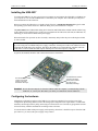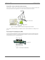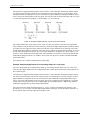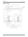
1
USB-2537 Multifunction Measurement and Control User's Guide Document Revision 6, January, 2011 © Copyright 2011, Measurement Computing Corporation Your new Measurement Computing product comes with a fantastic extra — Management committed to your satisfaction! Thank you for choosing a Measurement Computing product—and congratulations! You own the finest, and you can now enjoy the protection of the most comprehensive warranties and unmatched phone tech support. It’s the embodiment of our mission: To provide data acquisition hardware and software that will save time and save money. Simple installations minimize the time between setting up your system and actually making measurements. We offer quick and simple access to outstanding live FREE technical support to help integrate MCC products into a DAQ system. Limited Lifetime Warranty: Most MCC products are covered by a limited lifetime warranty against defects in materials or workmanship for the life of the product, to the original purchaser, unless otherwise noted. Any products found to be defective in material or workmanship will be repaired, replaced with same or similar device, or refunded at MCC’s discretion. For specific information, please refer to the terms and conditions of sale. Harsh Environment Program: Any Measurement Computing product that is damaged due to misuse, or any reason, may be eligible for replacement with the same or similar device for 50% of the current list price. I/O boards face some harsh environments, some harsher than the boards are designed to withstand. Contact MCC to determine your product’s eligibility for this program. 30 Day Money-Back Guarantee: Any Measurement Computing Corporation product may be returned within 30 days of purchase for a full refund of the price paid for the product being returned. If you are not satisfied, or chose the wrong product by mistake, you do not have to keep it. These warranties are in lieu of all other warranties, expressed or implied, including any implied warranty of merchantability or fitness for a particular application. The remedies provided herein are the buyer’s sole and exclusive remedies. Neither Measurement Computing Corporation, nor its employees shall be liable for any direct or indirect, special, incidental or consequential damage arising from the use of its products, even if Measurement Computing Corporation has been notified in advance of the possibility of such damages. Trademark and Copyright Information TracerDAQ, Universal Library, Measurement Computing Corporation, and the Measurement Computing logo are either trademarks or registered trademarks of Measurement Computing Corporation. Windows, Microsoft, and Visual Studio are either trademarks or registered trademarks of Microsoft Corporation LabVIEW is a trademark of National Instruments. CompactFlash is a registered trademark of SanDisk Corporation. XBee and XBee-PRO are trademarks of MaxStream, Inc. All other trademarks are the property of their respective owners. Information furnished by Measurement Computing Corporation is believed to be accurate and reliable. However, no responsibility is assumed by Measurement Computing Corporation neither for its use; nor for any infringements of patents or other rights of third parties, which may result from its use. No license is granted by implication or otherwise under any patent or copyrights of Measurement Computing Corporation. All rights reserved. No part of this publication may be reproduced, stored in a retrieval system, or transmitted, in any form by any means, electronic, mechanical, by photocopying, recording, or otherwise without the prior written permission of Measurement Computing Corporation. Notice Measurement Computing Corporation does not authorize any Measurement Computing Corporation product for use in life support systems and/or devices without prior written consent from Measurement Computing Corporation. Life support devices/systems are devices or systems which, a) are intended for surgical implantation into the body, or b) support or sustain life and whose failure to perform can be reasonably expected to result in injury. Measurement Computing Corporation products are not designed with the components required, and are not subject to the testing required to ensure a level of reliability suitable for the treatment and diagnosis of people. HM USB-2537.doc Table of Contents Preface About this User's Guide .......................................................................................................................6 What you will learn from this user's guide ......................................................................................................... 6 Conventions in this user's guide ......................................................................................................................... 6 Where to find more information ......................................................................................................................... 6 Chapter 1 Introducing the USB-2537 ....................................................................................................................7 Overview: USB-2537 features ............................................................................................................................ 7 Software features ................................................................................................................................................ 7 Chapter 2 Installing the USB-2537 ........................................................................................................................8 What comes with your USB-2537 shipment? ..................................................................................................... 8 Hardware .......................................................................................................................................................................... 8 Optional components ........................................................................................................................................................ 8 Signal conditioning accessories ........................................................................................................................................ 9 Additional documentation ................................................................................................................................................. 9 Unpacking the USB-2537 ................................................................................................................................... 9 Installing the software ........................................................................................................................................ 9 Installing the USB-2537 ................................................................................................................................... 10 Configuring the hardware ................................................................................................................................. 10 Connecting the board for I/O operations .......................................................................................................... 11 Connectors, cables – main I/O connector.........................................................................................................................11 68-pin SCSI connector differential and single-ended pin outs (P5) .................................................................................12 TB-100 terminal board connector to SCSI connector pin out ..........................................................................................14 40-pin header connector pin outs .....................................................................................................................................15 Four-channel TC terminal pin out (TB7) .........................................................................................................................18 Cabling ............................................................................................................................................................. 19 Field wiring and signal termination .................................................................................................................................20 Using multiple USB-2537s per PC ................................................................................................................... 20 Chapter 3 Functional Details ...............................................................................................................................21 USB-2537 components ..................................................................................................................................... 21 USB-2537 block diagram ................................................................................................................................. 23 Synchronous I/O – mixing analog, digital, and counter scanning .................................................................... 24 Analog input ..................................................................................................................................................... 24 Analog input scanning .....................................................................................................................................................24 Thermocouple input .......................................................................................................................................... 27 Tips for making accurate temperature measurements ......................................................................................................27 Analog output ................................................................................................................................................... 28 Digital I/O......................................................................................................................................................... 29 Digital input scanning ......................................................................................................................................................29 Digital outputs and pattern generation .............................................................................................................................30 Triggering ......................................................................................................................................................... 30 Hardware analog triggering .............................................................................................................................................30 Digital triggering..............................................................................................................................................................30 Software-based triggering ................................................................................................................................................31 Stop trigger modes ...........................................................................................................................................................31 Pre-triggering and post-triggering modes ........................................................................................................................31 4 USB-2537 User's Guide Counter inputs .................................................................................................................................................. 32 Mapped channels .............................................................................................................................................................32 Counter modes .................................................................................................................................................................33 Debounce modes ..............................................................................................................................................................34 Encoder mode ..................................................................................................................................................................37 Timer outputs.................................................................................................................................................... 41 Example: Timer outputs ...................................................................................................................................................41 Using detection setpoints for output control ..................................................................................................... 41 What are detection setpoints? ..........................................................................................................................................41 Setpoint configuration overview ......................................................................................................................................42 Setpoint configuration......................................................................................................................................................43 Using the setpoint status register......................................................................................................................................44 Examples of control outputs ............................................................................................................................................44 Detection setpoint details .................................................................................................................................................48 FIRSTPORTC, DAC, or timer update latency .................................................................................................................49 Mechanical drawing ......................................................................................................................................... 50 Chapter 4 Calibrating the USB-2537 ...................................................................................................................51 Chapter 5 Specifications ......................................................................................................................................52 Analog input ..................................................................................................................................................... 52 Accuracy ..........................................................................................................................................................................52 Thermocouples ................................................................................................................................................................53 Analog outputs.................................................................................................................................................. 53 Digital input/output........................................................................................................................................... 54 Counters............................................................................................................................................................ 54 Input sequencer ................................................................................................................................................. 55 Trigger sources and modes ............................................................................................................................... 56 Frequency/pulse generators .............................................................................................................................. 56 Power consumption .......................................................................................................................................... 56 External power.................................................................................................................................................. 57 USB specifications ........................................................................................................................................... 57 Environmental .................................................................................................................................................. 57 Mechanical ....................................................................................................................................................... 57 Signal I/O connectors and pin out .................................................................................................................... 57 68-pin SCSI connector pin outs .......................................................................................................................................58 40-pin header connector pin outs .....................................................................................................................................59 TC connector pin out (TB7) .............................................................................................................................................63 5 Preface About this User's Guide What you will learn from this user's guide This user's guide describes the Measurement Computing USB-2537 data acquisition device and lists the specifications. Conventions in this user's guide For more information on … Text presented in a box signifies additional information and helpful hints related to the subject matter you are reading. Caution! Shaded caution statements present information to help you avoid injuring yourself and others, damaging your hardware, or losing your data. bold text Bold text is used for the names of objects on a screen, such as buttons, text boxes, and check boxes. italic text Italic text is used for the names of manuals and help topic titles, and to emphasize a word or phrase. Where to find more information For additional information relevant to the operation of your hardware, refer to the Documents subdirectory where you installed the MCC DAQ software (C:\Program Files\Measurement Computing\DAQ by default), or search for your device on our website at www.mccdaq.com. 6 Chapter 1 Introducing the USB-2537 Overview: USB-2537 features The USB-2537 is supported under popular Microsoft® Windows® operating systems. The USB-2537 board is a multifunction measurement and control board designed for the USB bus. The USB-2537 provides either 32 differential or 64 single-ended analog inputs with 16-bit resolution from its 40-pin connectors. It offers seven software-selectable analog input ranges of ±10 V, ±5 V, ±2 V, ±1 V, ±0.5 V, ±0.2 V, and ±0.1V. You can configure up to four of the analog inputs as differential thermocouple (TC) inputs. The USB-2537 also has four 16-bit, 1 MHz analog output channels with an output range of -10 V to +10 V. The board has 24 high-speed lines of digital I/O, two timer outputs, and four 32-bit counters. It provides up to 4 MHz scanning on all digital input lines1. You can operate all analog I/O, digital I/O, and counter/timer I/O synchronously. Software features For information on the features of InstaCal and the other software included with your USB-2537, refer to the Quick Start Guide that shipped with your device. 1 Higher rates—up to 12 MHz—are possible depending on the platform and the amount of data being transferred. 7 Chapter 2 Installing the USB-2537 What comes with your USB-2537 shipment? As you unpack your USB-2537, verify that the following components are included. Hardware USB-2537 (with seven standoffs) USB cable (2-meter length) Optional components Cables and signal conditioning accessories that are compatible with the USB-2537 are not included with USB2537 orders, and must be ordered separately. If you ordered any of the following products with your board, they should be included with your shipment. 8 USB-2537 User's Guide Installing the USB-2537 PS-9V1AEPS-2500 power supply Cables CA-68-3R CA-68-6S (6-feet) CA-68-3S (3-feet) C40FF-x Signal conditioning accessories MCC provides signal termination products for use with the USB-2537. Refer to the "Field wiring and signal termination" section for a complete list of compatible accessory products. Additional documentation In addition to this hardware user's guide, you should also receive the Quick Start Guide (available in PDF at www.mccdaq.com/PDFmanuals/DAQ-Software-Quick-Start.pdf). This booklet supplies a brief description of the software you received with your USB-2537 and information regarding installation of that software. Please read this booklet completely before installing any software or hardware. Unpacking the USB-2537 As with any electronic device, you should take care while handling to avoid damage from static electricity. Before removing the USB-2537 from its packaging, ground yourself using a wrist strap or by simply touching the computer chassis or other grounded object to eliminate any stored static charge. If any components are missing or damaged, notify Measurement Computing Corporation immediately by phone, fax, or e-mail: Phone: 508-946-5100 and follow the instructions for reaching Tech Support. Fax: 508-946-9500 to the attention of Tech Support Email: [email protected] Installing the software Refer to the Quick Start Guide for instructions on installing the software on the Measurement Computing Data Acquisition Software CD. This booklet is available in PDF at www.mccdaq.com/PDFmanuals/DAQ-SoftwareQuick-Start.pdf. We recommend that you download the latest Windows Update onto your computer before installing and operating the USB-2537. 9 USB-2537 User's Guide Installing the USB-2537 Installing the USB-2537 To connect the USB-2537 to your system, turn your computer on, and connect the USB cable to a USB port on your computer or to an external USB hub that is connected to your computer. The USB cable provides power and communication to the USB-2537. When you connect the USB-2523 to a computer for the first time, a Found New Hardware dialog opens when the operating system detects the device. When the dialog closes, the installation is complete. The power LED (bottom LED) blinks during device detection and initialization, and then remains solid as long as the USB-2537 has sufficient power. If the power provided from the USB is not sufficient, the LED turns off, indicating you need a PS-9V1AEPS-2500 power supply. When the board is first powered on, there is usually a momentary delay before the power LED begins to blink, or come on solid. Connect external power, if used, before connecting the USB cable to the computer If you are using a PS-9V1AEPS-2500 power supply, connect the external power cable to the USB-2537 before connecting the USB cable to the computer. This allows the USB-2537 to inform the host computer (when the USB cable is connected) that the board requires minimal power from the computer’s USB port. In general, all standoffs should be used to mount the board to a metal frame. The standoff at this location connects to the USB2537’s internal chassis plane for shunting electrostatic discharge. The standoff at this location connects to the USB chassis for shunting electrostatic discharge. Caution! Do not disconnect any device from the USB bus while the computer is communicating with the USB-2537, or you may lose data and/or your ability to communicate with the USB-2537. Configuring the hardware All hardware configuration options on the USB-2537 are software-controlled. You can select some of the configuration options using InstaCal, such as the analog input configuration (64 single-ended or 32 differential channels), and the edge used for pacing when using an external clock. Once selected, any program that uses the Universal Library initializes the hardware according to these selections. You need a PS-9V1AEPS-2500 power supply (sold separately) when there is insufficient power from the USB port. However, you can use this power supply in any scenario. 10 USB-2537 User's Guide Installing the USB-2537 Caution! Avoid redundant connections. Ensure there is no signal conflict between SCSI pins and the associated header pin (J5 - J8). Also make sure there is no conflict between theTB7 TC connections and the SCSI and/or the 40-pin header connections. Failure to do so could possibly cause equipment damage and/or personal injury. Also, turn off power to all devices connected to the system before making connections. Electrical shock or damage to equipment can result even under low-voltage conditions. Information on signal connections General information regarding signal connection and configuration is available in the Guide to Signal Connections. This document is available on our web site at www.mccdaq.com/signals/signals.pdf. Caution! Always handle components carefully, and never touch connector pins or circuit components unless you are following ESD guidelines in an appropriate ESD-controlled area. These guidelines include using properly-grounded mats and wrist straps, ESD bags and cartons, and related procedures. Avoid touching board surfaces and onboard components. Only handle boards by their edges. Make sure the USB-2537 does not come into contact with foreign elements such as oils, water, and industrial particulate. The discharge of static electricity can damage some electronic components. Semiconductor devices are especially susceptible to ESD damage. Connecting the board for I/O operations Connectors, cables – main I/O connector The following table lists the board connectors, applicable cables, and compatible accessory products for the USB-2537. Board connectors, cables, and compatible hardware Parameter Specification Connector type Main connector: 68-pin standard "SCSI type III" female connector Auxiliary connectors: Four, 40-pin header connectors CA-68-3R — 68-pin ribbon cable; 3 feet. CA-68-3S — 68-pin shielded round cable; 3 feet. CA-68-6S — 68-pin shielded round cable; 6 feet C40FF-x TB-100 terminal connector Compatible cables — main connector Compatible cables — 40-pin connectors Compatible accessory products using the CA-68-3R, CA-68-3S, or CA-68-6S cables Compatible accessory products using the C40FF-x cable CIO-MINI40 11 USB-2537 User's Guide Installing the USB-2537 68-pin SCSI connector differential and single-ended pin outs (P5) The 68-pin SCSI connector—labeled P5 on the board—provides 16 single-ended analog channels or eight differential analog channels. Refer to the "40-pin header connector pin outs" section starting on page 15 to learn the pin outs for accessing up to 64 single-ended/32 differential analog channels using the P5 and P6 connectors. Caution! Avoid redundant connections. Make sure there is no signal conflict among the SCSI pins, the 40pin header connector pins (J5 - J8), and the TB7 TC connections. Failure to do so could possibly cause equipment damage and/or personal injury. 68-pin SCSI connector pin out (labeled P5 on the board) 16-channel single-ended mode Signal name ACH0 AGND ACH9 ACH2 AGND ACH11 SGND ACH12 ACH5 AGND ACH14 ACH7 XDAC3 XDAC2 NEGREF (reserved for self-calibration) GND A1 A3 A5 A7 B1 B3 B5 B7 C1 C3 C5 C7 GND CNT1 CNT3 TMR1 GND GND Pin Pin 68 67 66 65 64 63 62 61 60 59 58 57 56 55 54 53 52 51 50 49 48 47 46 45 44 43 42 41 40 39 38 37 36 35 34 33 32 31 30 29 28 27 26 25 24 23 22 21 20 19 18 17 16 15 14 13 12 11 10 9 8 7 6 5 4 3 2 1 12 Signal name ACH8 ACH1 AGND ACH10 ACH3 AGND ACH4 AGND ACH13 ACH6 AGND ACH15 XDAC0 XDAC1 POSREF (reserved for self-calibration) +5 V A0 A2 A4 A6 B0 B2 B4 B6 C0 C2 C4 C6 TTL TRG CNT0 CNT2 TMR0 XAPCR XDPCR USB-2537 User's Guide Installing the USB-2537 68-pin SCSI connector pin out (labeled P5 on the board) 8-channel differential mode Signal name ACH0 HI AGND ACH1 LO ACH2 HI AGND ACH3 LO SGND ACH4 LO ACH5 HI AGND ACH6 LO ACH7 HI XDAC3 XDAC2 NEGREF (reserved for self-calibration) GND A1 A3 A5 A7 B1 B3 B5 B7 C1 C3 C5 C7 GND CNT1 CNT3 TMR1 GND GND Pin Pin 68 67 66 65 64 63 62 61 60 59 58 57 56 55 54 53 52 51 50 49 48 47 46 45 44 43 42 41 40 39 38 37 36 35 34 33 32 31 30 29 28 27 26 25 24 23 22 21 20 19 18 17 16 15 14 13 12 11 10 9 8 7 6 5 4 3 2 1 13 Signal name ACH0 LO ACH1 HI AGND ACH2 LO ACH3 HI AGND ACH4 HI AGND ACH5 LO ACH6 HI AGND ACH7 LO XDAC0 XDAC1 POSREF (reserved for self-calibration) +5 V A0 A2 A4 A6 B0 B2 B4 B6 C0 C2 C4 C6 TTL TRG CNT0 CNT2 TMR0 XAPCR XDPCR USB-2537 User's Guide Installing the USB-2537 TB-100 terminal board connector to SCSI connector pin out SCSI connector pin out assignments for TB-7 terminal board connector (differential analog signals in parentheses) TB2 screw terminals +5V GND A0 A1 A2 A3 A4 A5 A6 A7 B0 B1 B2 B3 B4 B5 B6 B7 C0 C1 C2 C3 C4 C5 C6 C7 TTLTRG GND CNT0 CNT1 CNT2 CNT3 TMR0 TMR1 XDPCR GND SCSI pin TB1 screw terminal SCSI pin 19 ACH0 (ACH0 HI) ACH8 (ACH0 LO) AGND ACH1 (ACH1 HI) ACH9 (ACH1 LO) AGND ACH2 (ACH2 HI) ACH10 (ACH2 LO) AGND ACH3 (ACH3 HI) ACH11 (ACH3 LO) AGND ACH4 (ACH4 HI) ACH12 (ACH4 LO) AGND ACH5 (ACH5 HI) ACH13 (ACH5 LO) AGND ACH6 (ACH6 HI) ACH14 (ACH6 LO) AGND ACH7 (ACH7 HI) ACH15 (ACH7 LO) XDAC3 SGND POSREF (reserved for self-calibration) XDAC2 NEGREF (reserved for self-calibration) AGND XDAC0 AGND XDAC1 AGND XAPCR GND EGND 68 34 ** 33 66 ** 65 31 ** 30 63 ** 28 61 ** 60 26 ** 25 58 ** 57 23 56 62 20 55 54 ** 22 ** 21 ** 2 ** † * 18 52 17 51 16 50 15 49 14 48 13 47 12 46 11 45 10 44 9 43 8 42 7 41 6 * 5 39 4 38 3 37 1 * * Digital common ground pins on the SCSI connector are: 35, 36, and 40. ** Analog common ground pins on the SCSI connector are: 24, 27, 29, 32, 59, 64, and 67. † EGND is connected to the SCSI connector shell. 14 USB-2537 User's Guide Installing the USB-2537 40-pin header connector pin outs Analog channels pin out (J5 and J6) This edge of the header is closest to the center of the USB2537. Pins 2 and 40 are labeled on the board silkscreen. 40-pin header connectors pin out (labeled J5 and J6) 64-channel single-ended mode Analog channel Pin J5 Pin Analog channel Analog channel Pin J6 Pin Analog channel ACH27 1 2 ACH19 ACH43 1 2 ACH59 ACH26 3 4 ACH18 ACH35 3 4 ACH51 AGND 5 6 AGND AGND 5 6 ACH58 ACH3 7 8 ACH11 ACH42 7 8 ACH50 ACH2 9 10 ACH10 ACH34 9 10 ACH57 ACH17 11 12 ACH25 AGND 11 12 ACH49 ACH16 13 14 ACH24 ACH41 13 14 ACH56 ACH1 15 16 ACH9 ACH33 15 16 ACH48 ACH0 17 18 ACH8 ACH40 17 18 AGND AGND 19 20 AGND ACH32 19 20 ACH63 ACH23 21 22 ACH31 ACH47 21 22 ACH55 ACH22 23 24 ACH30 ACH39 23 24 AGND ACH7 25 26 ACH15 ACH46 25 26 ACH62 ACH6 27 28 ACH14 ACH38 27 28 ACH54 AGND 29 30 ACH21 AGND 29 30 ACH61 ACH29 31 32 ACH20 ACH45 31 32 ACH53 ACH28 33 34 ACH5 ACH37 33 34 ACH60 ACH13 35 36 ACH4 ACH44 35 36 ACH52 ACH12 37 38 AGND ACH36 37 38 AGND AGND 39 40 AGND AGND 39 40 AGND 15 USB-2537 User's Guide Installing the USB-2537 40-pin header connectors pin out (labeled J5 and J6) 32-channel differential mode Analog channel Pin J5 Pin Analog channel Analog channel Pin J6 Pin Analog channel ACH11 LO 1 2 ACH11 HI ACH19 LO 1 2 ACH27 LO ACH10 LO 3 4 ACH10 HI ACH19 HI 3 4 ACH27 HI AGND 5 6 AGND AGND 5 6 ACH26 LO ACH3 HI 7 8 ACH3 LO ACH18 LO 7 8 ACH26 HI ACH2 HI 9 10 ACH2 LO ACH18 HI 9 10 ACH25 LO ACH9 HI 11 12 ACH9 LO AGND 11 12 ACH25 HI ACH8 HI 13 14 ACH8 LO ACH17 LO 13 14 ACH24 LO ACH1 HI 15 16 ACH1 LO ACH17 HI 15 16 ACH24 HI ACH0 HI 17 18 ACH0 LO ACH16 LO 17 18 AGND AGND 19 20 AGND ACH16 HI 19 20 ACH31 LO ACH15 HI 21 22 ACH15 LO ACH23 LO 21 22 ACH31 HI ACH14 HI 23 24 ACH14 LO ACH23 HI 23 24 AGND ACH7 HI 25 26 ACH7 LO ACH22 LO 25 26 ACH30 LO ACH6 HI 27 28 ACH6 LO ACH22 HI 27 28 ACH30 HI AGND 29 30 ACH13 HI AGND 29 30 ACH29 LO ACH13 LO 31 32 ACH12 HI ACH21 LO 31 32 ACH29 HI ACH12 LO 33 34 ACH5 HI ACH21 HI 33 34 ACH28 LO ACH5 LO 35 36 ACH4 HI ACH20 LO 35 36 ACH28 HI ACH4 LO 37 38 AGND ACH20 HI 37 38 AGND AGND 39 40 AGND AGND 39 40 AGND 16 USB-2537 User's Guide Installing the USB-2537 Digital ports, counters, timers, DACs, triggers, and pacer clocks pin out (J7 and J8) You can use the 40-pin connector headers labeled J7 and J8 to connect digital ports, counters, timers, DACs, triggers, pacer clocks, and other signals. USB-2537 40-pin header connectors pin out (labeled J7 and J8) Digital channel Pin J7 Pin Digital channel Signal Pin +13 V 1 2 -13 V J8 Pin Signal GND 1 2 XAPCR A0 3 4 A4 NC 3 4 NC A1 5 6 A5 AGND 5 6 AGND A2 7 8 A6 XDAC0 7 8 XDAC2 A3 9 10 A7 XDAC1 9 10 XDAC3 GND 11 12 TTL TRG AGND 11 12 AGND B0 13 14 B4 SelfCal 13 14 SGND B1 15 16 B5 AGND 15 16 AGND B2 17 18 B6 TTL TRG 17 18 XDPCR B3 19 20 B7 XAPCR 19 20 GND (digital) GND 21 22 +5 V GND (digital) 21 22 GND (digital) C0 23 24 C4 NC 23 24 NC C1 25 26 C5 +5 V 25 26 AUX PWR C2 27 28 C6 NC 27 28 NC C3 29 30 C7 NC 29 30 NC GND 31 32 TMR1 NC 31 32 NC TMR0 33 34 CNT1 NC 33 34 NC CNT0 35 36 CNT3 NC 35 36 NC CNT2 37 38 GND NC 37 38 NC GND 39 40 GND NC 39 40 NC 17 USB-2537 User's Guide Installing the USB-2537 Using C40FF-x cables to obtain 40-pin female connectors In this example, a C40FF-x cable is connected to all of the 40-pin headers (J5, J6, J7, and J8). The result is four female 40-pin connectors that together have more signal connectivity than the SCSI connector. 40-pin female connectors C40FF-x header cables USB cable Figure 1. Four C40FF-x cables connected to J5 through J8 40-pin connectors In all scenarios, a USB cable (MCC p/n CA-USB2.0) is used to connect the USB-2537 to a USB port on the host PC. Four-channel TC terminal pin out (TB7) You can use the TB7 terminal block to connect up to four thermocouples. The first TC channel uses ACH0 (analog channel 0) for its positive (+) lead, and ACH8 for its negative (-) lead. The second TC channel uses ACH1 and ACH9, and so on, as indicated in Figure 2. TC CH 0 TC CH 1 TC CH 2 TC CH 3 Standoff AGND ACH0 + ACH8 (-) ACH1 + ACH9 (-) ACH2 + ACH10 (-) ACH3 + ACH11 (-) Figure 2. TC terminal pin out (labeled TB7) 18 USB-2537 User's Guide Installing the USB-2537 Cabling Use a CA-68-3R 68-pin ribbon expansion cable (Figure 3), or a CA-68-3S (3-foot) or CA-68-6S (6-foot) 68-pin shielded expansion cable (Figure 4) to connect signals to the USB-2537's 68-pin SCSI connector. 34 68 1 35 34 68 1 35 The stripe identifies pin # 1 Figure 3. CA-68-3R cable 34 68 1 35 34 68 1 35 Figure 4. CA-68-3S and CA-68-6S cable Use one or more C40FF-x- ribbon cable(s) (Figure 5) to connect signals to one or more of the USB-2537's 40pin header connectors. 2 40 The red stripe identifies pin # 1 1 2 40 39 40-pin Female IDC Connector 1 39 40-pin Female IDC Connector Figure 5. C40FF-x cable 19 USB-2537 User's Guide Installing the USB-2537 Field wiring and signal termination You can use the following Measurement Computing screw terminal board to terminate field signals and route them into the USB-2537 board using the CA-68-3R, CA-68-3S, or CA-68-6S cable: TB-100: Termination board with screw terminals. A 19-inch rack mount kit (RM-TB-100) for the TB-100 termination board is also available. You can use the following screw terminal board with the C40FF-x cable. CIO-MINI40: 40-pin screw terminal board. Details on these products are available on our web site. Using multiple USB-2537s per PC USB-2537 features can be replicated up to four times, as up to four devices can be connected a single host PC. The serial number on each USB-2537 distinguishes one from another. You can operate multiple USB-2537 boards synchronously. To do this, set up one USB-2537 with the pacer pin you want to use (XAPCR or XDPCR) configured for output. Set up the USB-2537 boards you want to synchronize to this board with the pacer pin you want to use (XAPCR or XDPCR) configured for input. Wire the pacer pin configured for output to each of the pacer input pins that you want to synchronize. 20 Chapter 3 Functional Details This chapter contains detailed information on all of the features available from the board, including: a diagram and explanations of physical board components a functional block diagram information on how to use the signals generated by the board diagrams of signals using default or conventional board settings USB-2537 components These USB-2537 components are shown in Figure 6. One USB port One external power connector One 68-pin SCSI connector Four 40-pin headers (J5, J6, J7, and J8) One four-channel TC screw terminal block Two LED indicators (USB and power) J6 TB7 J5 J7 J8 P5 External power supply connector USB 2.0 port USB LED Power LED Figure 6. USB-2537 components 21 USB-2537 User's Guide Functional Details SCSI - 68 pin (P5) connector The 68-pin SCSI connector includes pins for the following: 16 single-ended/eight differential analog inputs (64 single-ended/32 differential analog inputs available only from J5 and J6 40-pin connectors) Four analog outputs 24 digital I/O Four counter inputs Two timer outputs Input scan pacer clock I/O Output scan pacer clock I/O TTL trigger self calibration +5 VDC analog commons digital commons 40-pin headers (J5, J6, J7, J8) Four 40-pin headers (J5 through J8) provide alternative connections to the signals of the SCSI connector. Up to 64 single-ended/32 differential analog inputs are available from J5 and J6 connectors as well. You can get a female connector for each header by connecting a C40FF-x cable (40-pin header to female 40-pin header) to each header. 9-slot screw terminal (TB7) You can use the on-board screw terminal connector (TB7) to connect up to four TC inputs. TB7 uses the following analog channels to obtain its four differential channels: TC CH0: CH 0 (+); CH 8 (-) TC CH1: CH 1 (+); CH 9 (-) TC CH2: CH 2 (+); CH 10 (-) TC CH3: CH 3 (+); CH 11 (-) When using the thermocouple channels, do not connect signals to the associated channels on the SCSI connector or J5. External power connector Although the USB-2537 is powered by a USB port on a host PC, an external power connector is available when the host PC’s USB port cannot supply adequate power, or if you prefer to use a separate power source. Connect the optional PS-9V1AEPS-2500 power supply to the external power supply connector. This power supply plugs into a standard 120 VAC outlet and supplies 9 VDC, 1 A power to the USB-2537. 22 USB-2537 User's Guide Functional Details USB-2537 block diagram Figure 7 is a simplified block diagram of the USB-2537. This board provides all of the functional elements shown in the figure. Figure 7. USB-2537 functional block diagram 23 USB-2537 User's Guide Functional Details Synchronous I/O – mixing analog, digital, and counter scanning The USB-2537 can read analog, digital, and counter inputs, while generating up to four analog outputs and digital pattern outputs at the same time. Digital and counter inputs do not affect the overall A/D rate because these inputs use no time slot in the scanning sequencer. For example, one analog input channel can be scanned at the full 1 MHz A/D rate along with digital and counter input channels. Each analog channel can have a different gain, and counter and digital channels do not need additional scanning bandwidth as long as there is at least one analog channel in the scan group. Digital input channel sampling is not done during the "dead time" of the scan period where no analog sampling is being done either. Analog input The USB-2537 has a 16-bit, 1-MHz A/D coupled with 64 single-ended, or 32 differential analog inputs. Seven software programmable ranges provide inputs from ±10 V to ±100 mV full scale. Analog input scanning The USB-2537 has several scanning modes to address various applications. You can load the 512-location scan buffer with any combination of analog input channels. All analog input channels in the scan buffer are measured sequentially at 1 µs per channel by default. For example, in the fastest mode, with a 1 µs settling time for the acquisition of each channel, a single analog channel can be scanned continuously at 1 MS/s; two analog channels can be scanned at 500 kS/s each; 16 analog input channels can be scanned at 62.5 kS/s. Settling time For most applications, leave the settling time at its default of 1 µs. However, if you are scanning multiple channels, and one or more channels are connected to a high-impedance source, you may get better results by increasing the settling time. Remember that increasing the settling reduces the maximum acquisition rate. You can set the settling time to 1 µs, 5 µs, 10 µs, or 1 ms. Example: Analog channel scanning of voltage inputs Figure 8 shows a simple acquisition. The scan is programmed pre-acquisition and is made up of six analog channels (Ch0, Ch1, Ch3, Ch4, Ch6, and Ch7). Each of these analog channels can have a different gain. The acquisition is triggered and the samples stream to the PC. Using the default settling time, each analog channel requires one microsecond of scan time—therefore the scan period can be no shorter than 6 µs for this example. The scan period can be made much longer than 6 µs—up to 1 s. The maximum scan frequency is 1 divided by 6 µs, or 166,666 Hz. 24 USB-2537 User's Guide Functional Details Figure 8. Analog channel scan of voltage inputs example Example: Analog channel scanning of voltage and temperature inputs Figure 9 shows a programmed pre-acquisition scan made up of six analog channels (Ch0, Ch1, Ch5, Ch11, Ch12, Ch13). Each of these analog channels can have a different gain. You can program channels 0 and 1 to directly measure TCs. In this mode, oversampling is programmable up to 16384 oversamples per channel in the scan group. When oversampling is applied, it is applied to all analog channels in the scan group, including temperature and voltage channels. Digital channels are not oversampled. If you want 256 oversamples, then each analog channel in the scan group takes 256 µs, and the returned 16-bit value represents an average of 256 consecutive 1 µs samples of that channel. The acquisition is triggered and 16-bit values—each representing an average of 256—stream to the PC via the USB cable. Since two of the channels in the scan group are temperature channels, you need the acquisition engine to read a cold-junctioncompensation (CJC) temperature every scan. Figure 9. Analog channel scanning of voltage and temperature inputs example Since the targeted number of oversamples is 256 in this example, each analog channel in the scan group requires 256 microseconds to return one 16-bit value. The oversampling is also done for CJC temperature measurement channels, making the minimum scan period for this example 7 X 256 µs, or 1792 µs. The maximum scan frequency is the inverse of this number, 558 Hz. For accurate measurements, you must associate TC and CJC channels properly The TC channels must immediately follow their associated CJC channels in the channel array. For accurate TC readings, associate CJC0 with TC0, CJC1 with TC1 and TC2, and CJC2 with TC3. Example: Analog and digital scanning, once per scan mode The scan is programmed pre-acquisition and is made up of six analog channels (Ch0, Ch2, Ch5, Ch11, Ch13, Ch15) and four digital channels (16-bits of digital IO, three counter inputs.) Each of the analog channels can have a different gain. 25 USB-2537 User's Guide Functional Details The acquisition is triggered and the samples stream to the PC via the USB cable. Each analog channel requires one microsecond of scan time. Therefore, the scan period can be no shorter than 6 µs for this example. All of the digital channels are sampled at the start of scan and do not require additional scanning bandwidth as long as there is at least one analog channel in the scan group. The scan period can be made much longer than 6 µs, up to 1 second. The maximum scan frequency is one divided by 6 µs, or 166,666 Hz. Figure 10. Analog and digital scanning, once per scan mode example The counter channels may return only the lower 16-bits of count value if that is sufficient for the application. They could also return the full 32-bit result if necessary. Similarly, the digital input channel could be the full 24 bits if desired or only eight bits if that is sufficient. If the three counter channels are all returning 32-bit values and the digital input channel is returning a 16-bit value, then 13 samples are being returned to the PC every scan period, with each sample being 16-bits. The 32-bit counter channels are divided into two 16-bit samples—one for the low word, and the other for the high word. If the maximum scan frequency is 166,666 Hz, then the data bandwidth streaming into the PC is 2.167 MS/s. Some slower PCs may have a problem with data bandwidths greater than 6 MS/s. The USB-2537 has an onboard 1 MS buffer for acquired data. Example: Sampling digital inputs for every analog sample in a scan group The scan is programmed pre-acquisition and is made up of six analog channels (Ch0, Ch2, Ch5, Ch11, Ch13, Ch15) and four digital channels (16-bits of digital input, three counter inputs.) Each of the analog channels can have a different gain. The acquisition is triggered and the samples stream to the PC via the USB cable. Each analog channel requires one microsecond of scan time therefore the scan period can be no shorter than 6 µs for this example. All of the digital channels are sampled at the start of scan and do not require additional scanning bandwidth as long as there is at least one analog channel in the scan group. The 16-bits of digital input are sampled for every analog sample in the scan group. This allows up to 1 MHz digital input sampling while the 1 MHz analog sampling bandwidth is aggregated across many analog input channels. The scan period can be made much longer than 6 µs—up to 1 second. The maximum scan frequency is one divided by 6 µs, or 166,666 Hz. Note that digital input channel sampling is not done during the "dead time" of the scan period where no analog sampling is being done either. 26 USB-2537 User's Guide Functional Details Figure 11. Analog and digital scanning, once per scan mode example If the three counter channels are all returning 32-bit values and the digital input channel is returning a 1-bit value, then 18 samples are returned to the PC every scan period, with each sample being 16-bits. Each 32-bit counter channel is divided into two 16-bit samples—one for the low word and the other for the high word. If the maximum scan frequency is 166,666 Hz, then the data bandwidth streaming into the PC is 3 MS/s. Some slower PCs may have a problem with data bandwidths greater than 6 MS/s. The USB-2537 has an onboard 1 MS buffer for acquired data. Thermocouple input You can configure up to four analog inputs on the USB-2537 to accept a TC input. Built-in cold-junction sensors are provided for each of the screw-terminal connectors, and any TC type can be attached to any of the four thermocouple channels. When measuring TCs, the USB-2537 can operate in an averaging mode, taking multiple readings on each channel, applying digital filtering and cold-junction compensation, and then converting the readings to temperature. As a result, the USB-2537 measures channels with TCs attached at a rate from 50 Hz to 10 kHz, depending on how much over-sampling is selected. Additionally, a rejection frequency can be specified in which over sampling occurs during one cycle of either 50 Hz or 60 Hz, providing a high level of 50 Hz or 60 Hz rejection. Tips for making accurate temperature measurements Use as much oversampling as possible. Warm up the USB-2537 for 60 minutes—including TC wires—so that it is thermally stabilized. This warm-up time enables the CJC thermistors to more accurately measure the junction at the terminal block. Make sure the surrounding environment is thermally stabilized and ideally around 20 °C to 30 °C. If the board’s ambient temperature is changing due to a local heating or cooling source, then the TC junction temperature may be changing and the CJC thermistor will have a larger error. Use small-diameter, instrument-grade TC wire. Small diameter TC wire has less effect on the TC junction at the terminal block because less heat is transferred from the ambient environment to the junction. Use shielded TC wire (see "Shielding" on page 28) with the shield connected to analog common to reduce noise. The USB-2537 has several analog common pins on both the 68-pin connector and the 40-pin connectors, and the TB-7 has one analog common screw terminal. You can also minimize the effect of noise by averaging readings (see "Averaging" on page 28), or combining both shielding and averaging. Refer to "68-pin SCSI connector differential and single-ended pin outs (P5)" on page 12, "40-pin header connector pin outs" on page 15, and "Four-channel TC terminal pin out (TB7)" on page 18 for the locations of these analog common pins. 27 USB-2537 User's Guide Functional Details Make sure the USB-2537 is mounted on a flat surface. Be careful to avoid loading down the digital outputs too heavily (>1 mA). Heavy load down causes significant heat generation inside the unit and increase the CJC thermistor error. Shielding Use shielded TC wire with the shield connected to analog common to further reduce noise. The USB-2537 has one analog common screw-terminal on TB7 and several analog common pins on the headers (see "Connecting the board for I/O operations" starting on page 11). You can connect the shield of a shielded thermocouple to one of the analog commons. When this connection is made, leave the shield at the other end of the thermocouple unconnected. Caution! Connecting the shield to common at both ends results in a ground loop. Averaging Certain acquisition programs apply averaging after several samples have been collected. Depending on the nature of the noise, averaging can reduce noise by the square root of the number of averaged samples. Although averaging can be effective, it suffers from several drawbacks. Noise in measurements only decreases as the square root of the number of measurements—reducing RMS noise significantly may require many samples. Thus, averaging is suited to low-speed applications that can provide many samples. Only random noise is reduced or eliminated by averaging. Averaging does not reduce or eliminate periodic signals. Analog output The USB-2537 has four 16-bit, 1 MHz analog output channels. The channels have an output range of -10V to +10V. Each D/A output can continuously output a waveform at up to 1 MHz. In addition, a program can asynchronously output a value to any of the D/A channels for nonwaveform applications, assuming that the D/A is not already being used in the waveform output mode. When used to generate waveforms, you can clock the D/As in several different modes. Internal output scan clock: The on-board programmable clock can generate updates ranging from 1 Hz to 1 MHz. External output scan clock (XDPCR): A user-supplied external clock. Internal input scan pacer clock: The internal ADC pacer clock can pace both the D/A and the analog input. External input scan pacer clock (XAPCR): The external ADC pacer clock can pace both the D/A and the analog input. Example: Analog channel scanning of voltage inputs and streaming analog outputs The example shown in Figure 12 adds four DACs and a 16-bit digital pattern output paced by the input scan clock to the example presented in Figure 8. 28 USB-2537 User's Guide Functional Details Figure 12. Analog channel scan of voltage inputs and streaming analog outputs example This example updates all DACs and the 16-bits of digital I/O. These updates happen at the same time as the acquisition pacer clock—also called the input scan clock. All DACs and the 16-bits of pattern digital output are updated at the beginning of each scan. Due to the time it takes to shift the digital data out to the DACs, plus the actual settling time of the digital-toanalog conversion, the DACs actually take up to 4 µs after the start of scan to settle on the updated value. The data for the DACs and pattern digital output comes from a PC-based buffer. The data is streamed across the USB2 bus to the USB-2537. In this example, the outputs are updated by the input scan clock, but you can also update the DACs and pattern digital output with the output scan clock—either internally-generated or externally-applied. In this scenario, the acquisition input scans are not synchronized to the analog outputs or pattern digital outputs. Digital I/O Twenty-four TTL-level digital I/O lines are included in each USB-2537. You can program digital I/O in 8-bit groups as either inputs or outputs and scan them in several modes (see "Digital input scanning" below). You can access input ports asynchronously from the PC at any time, including when a scanned acquisition is occurring. Digital input scanning Digital input ports can be read asynchronously before, during, or after an analog input scan. Digital input ports can be part of the scan group and scanned along with analog input channels. Two synchronous modes are supported when digital inputs are scanned along with analog inputs. Refer to "Example 4: Sampling digital inputs for every analog sample in a scan group" on page 26 for more information. In both modes, adding digital input scans has no affect on the analog scan rate limitations. If no analog inputs are being scanned, the digital inputs can sustain rates up to 4 MHz. Higher rates—up to 12 MHz—are possible depending on the platform and the amount of data being transferred. 29 USB-2537 User's Guide Functional Details Digital outputs and pattern generation Digital outputs can be updated asynchronously at anytime before, during, or after an acquisition. You can use two of the 8-bit ports to generate a digital pattern at up to 4 MHz. The USB-2537 supports digital pattern generation. The digital pattern can be read from PC RAM. Higher rates—up to 12 MHz—are possible depending on the platform and the amount of data being transferred. Digital pattern generation is clocked using an internal clock. The on-board programmable clock generates updates ranging from once every 1 second to 1 MHz, independent of any acquisition rate. Triggering Triggering can be the most critical aspect of a data acquisition application. The USB-2537 supports the following trigger modes to accommodate certain measurement situations. Hardware analog triggering The USB-2537 uses true analog triggering in which the trigger level you program sets an analog DAC, which is then compared in hardware to the analog input level on the selected channel. This guarantees an analog trigger latency that is less than 1 µs. You can select any analog channel as the trigger channel, but the selected channel must be the first channel in the scan. You can program the trigger level, the rising or falling edge, and hysteresis. A note on the hardware analog level trigger and comparator change state When analog input voltage starts near the trigger level, and you are performing a rising or falling hardware analog level trigger, the analog level comparator may have already tripped before the sweep was enabled. If this is the case, the circuit waits for the comparator to change state. However, since the comparator has already changed state, the circuit does not see the transition. To resolve this problem, do the following: 1. Set the analog level trigger to the threshold you want. 2. Apply an analog input signal that is more than 2.5% of the full-scale range away from the desired threshold. This ensures that the comparator is in the proper state at the beginning of the acquisition. 3. Bring the analog input signal toward the desired threshold. When the input signal is at the threshold (± some tolerance) the sweep will be triggered. 4. Before re-arming the trigger, move the analog input signal to a level that is more than 2.5% of the full-scale range away from the desired threshold. For example, if you are using the ±2 V full-scale range (gain = 5), and you want to trigger at +1 V on the rising edge, you would set the analog input voltage to a start value that is less than +0.9 V (1 V – (2 V * 2 * 2.5%)). Digital triggering A separate digital trigger input line is provided (TTL TRG), allowing TTL-level triggering with latencies guaranteed to be less than 1 µs. You can program both of the logic levels (1 or 0) and the rising or falling edge for the discrete digital trigger input. 30 USB-2537 User's Guide Functional Details Software-based triggering The three software-based trigger modes differ from hardware analog triggering and digital triggering because the readings—analog, digital, or counter—are checked by the PC in order to detect the trigger event. Analog triggering You can select any analog channel in the scan as the trigger channel. You can program the trigger level, the rising or falling edge, and hysteresis. Pattern triggering You can select any scanned digital input channel pattern to trigger an acquisition, including the ability to mask or ignore specific bits. Counter triggering You can program triggering to occur when one of the counters meets or exceeds a set value, or is within a range of values. You can program any of the included counter channels as the trigger source. Software-based triggering usually results in a long period of inactivity between the trigger condition being detected and the data being acquired. However, the USB-2537 avoids this situation by using pre-trigger data. When software-based-triggering is used, and the PC detects the trigger condition—which may be thousands of readings after the actual occurrence of the signal—the USB-2537 driver automatically looks back to the location in memory where the actual trigger-causing measurement occurred, and presents the acquired data that begins at the point where the trigger-causing measurement occurs. The maximum inactive period in this mode equals one scan period. Set pre-trigger > 0 when using counter as trigger source When using a counter for a trigger source, you should use a pre-trigger with a value of at least 1. Since all counters start at zero with the first scan, there is no valid reference in regard to rising or falling edge. Setting a pre-trigger to 1 or more ensures that a valid reference value is present, and that the first trigger will be legitimate. Stop trigger modes You can use any of the software trigger modes explained previously to stop an acquisition. For example, you can program an acquisition to begin on one event—such as a voltage level—and then stop on another event—such as a digital pattern. Pre-triggering and post-triggering modes The USB-2537 supports four modes of pre-triggering and post-triggering, providing a wide-variety of options to accommodate any measurement requirement. When using pre-trigger, you must use software-based triggering to initiate an acquisition. No pre-trigger, post-trigger stop event In this simple mode, data acquisition starts when the trigger is received, and the acquisition stops when the stoptrigger event is received. 31 USB-2537 User's Guide Functional Details Fixed pre-trigger with post-trigger stop event In this mode, you set the number of pre-trigger readings to acquire. The acquisition continues until a stoptrigger event occurs. No pre-trigger, infinite post-trigger In this mode, no pre-trigger data is acquired. Instead, data is acquired beginning with the trigger event, and is terminated when you issue a command to halt the acquisition. Fixed pre-trigger with infinite post-trigger You set the amount of pre-trigger data to acquire. Then, the system continues to acquire data until the program issues a command to halt acquisition. Counter inputs Four 32-bit counters are built into the USB-2537. Each counter accepts frequency inputs up to 20 MHz. USB-2537 counter channels can be configured as standard counters or as multi-axis quadrature encoders. The counters can concurrently monitor time periods, frequencies, pulses, and other event driven incremental occurrences directly from pulse-generators, limit switches, proximity switches, and magnetic pick-ups. Counter inputs can be read asynchronously under program control, or synchronously as part of an analog or digital scan group. When reading synchronously, all counters are set to zero at the start of an acquisition. When reading asynchronously, counters may be cleared on each read, count up continually, or count until the 16 bit or 32 bit limit has been reached. See the counter mode descriptions below. Figure 13. Typical USB-2537 counter channel Mapped channels A mapped channel is one of four counter input signals that can get multiplexed into a counter module. The mapped channel can participate with the counter's input signal by gating the counter, latching the counter, and so on. The four possible choices for the mapped channel are the four counter input signals (post-debounce). A mapped channel can be used to: gate the counter decrement the counter latch the current count to the count register Usually, all counter outputs are latched at the beginning of each scan within the acquisition. However, you can use a second channel—known as the mapped channel—to latch the counter output. 32 USB-2537 User's Guide Functional Details Counter modes A counter can be asynchronously read with or without clear on read. The asynchronous read-signals strobe when the lower 16-bits of the counter are read by software. The software can read the counter's high 16-bits some time later after reading the lower 16-bits. The full 32-bit result reflects the timing of the first asynchronous read strobe. Totalize mode The Totalize mode allows basic use of a 32-bit counter. While in this mode, the channel's input can only increment the counter upward. When used as a 16-bit counter (counter low), one channel can be scanned at the 12 MHz rate. When used as a 32-bit counter (counter high), two sample times are used to return the full 32-bit result. Therefore a 32-bit counter can only be sampled at a 6 MHz maximum rate. If you only want the upper 16 bits of a 32-bit counter, then you can acquire that upper word at the 12 MHz rate. The counter counts up and does not clear on every new sample. However, it does clear at the start of a new scan command. The counter rolls over on the 16-bit (counter low) boundary, or on the 32-bit (counter high) boundary. Clear on read mode The counter counts up and is cleared after each read. By default, the counter counts up and only clears the counter at the start of a new scan command. The final value of the counter —the value just before it was cleared—is latched and returned to the USB-2537. Stop at the top mode The counter stops at the top of its count. The top of the count is FFFF hex (65,535) for the 16-bit mode, and FFFFFFFF hex (4,294,967,295) for the 32-bit mode. 32-bit or 16-bit Sets the counter type to either 16-bits or 32-bits. The type of counter only matters if the counter is using the stop at the top mode—otherwise, this option is ignored. Latch on map Sets the signal on the mapped counter input to latch the count. By default, the start of scan signal—a signal internal to the USB-2537 pulses once every scan period to indicate the start of a scan group—latches the count, so the count is updated each time a scan is started. Gating "on" mode Sets the gating option to "on" for the mapped channel, enabling the mapped channel to gate the counter. Any counter can be gated by the mapped channel. When the mapped channel is high, the counter is enabled. When the mapped channel is low, the counter is disabled (but holds the count value). The mapped channel can be any counter input channel other than the counter being gated. Decrement "on" mode Sets the counter decrement option to "on" for the mapped channel. The input channel for the counter increments the counter, and you can use the mapped channel to decrement the counter. 33 USB-2537 User's Guide Functional Details Debounce modes Each channel's output can be debounced with 16 programmable debounce times from 500 ns to 25.5 ms. The debounce circuitry eliminates switch-induced transients typically associated with electro-mechanical devices including relays, proximity switches, and encoders. There are two debounce modes, as well as a debounce bypass, as shown in Figure 14. In addition, the signal from the buffer can be inverted before it enters the debounce circuitry. The inverter is used to make the input rising-edge or falling-edge sensitive. Edge selection is available with or without debounce. In this case the debounce time setting is ignored and the input signal goes straight from the inverter or inverter bypass to the counter module. There are 16 different debounce times. In either debounce mode, the debounce time selected determines how fast the signal can change and still be recognized. The two debounce modes are trigger after stable and trigger before stable. A discussion of the two modes follows. Figure 14. Debounce model block diagram Trigger after stable mode In the trigger after stable mode, the output of the debounce module does not change state until a period of stability has been achieved. This means that the input has an edge, and then must be stable for a period of time equal to the debounce time. Figure 15. Debounce module – trigger after stable mode The following time periods (T1 through T5) pertain to Figure 15. In trigger after stable mode, the input signal to the debounce module is required to have a period of stability after an incoming edge, in order for that edge to be accepted (passed through to the counter module.) The debounce time for this example is equal to T2 and T5. T1 – In the example above, the input signal goes high at the beginning of time period T1, but never stays high for a period of time equal to the debounce time setting (equal to T2 for this example.) 34 USB-2537 User's Guide Functional Details T2 – At the end of time period T2, the input signal has transitioned high and stayed there for the required amount of time—therefore the output transitions high. If the input signal does not stabilize in the high state long enough, no transition would have appeared on the output and the entire disturbance on the input would have been rejected. T3 – During time period T3, the input signal remained steady. No change in output is seen. T4 – During time period T4, the input signal has more disturbances and does not stabilize in any state long enough. No change in the output is seen. T5 – At the end of time period T5, the input signal has transitioned low and stayed there for the required amount of time—therefore the output goes low. Trigger before stable mode In the trigger before stable mode, the output of the debounce module immediately changes state, but will not change state again until a period of stability has passed. For this reason the mode can be used to detect glitches. Figure 16. Debounce module – Trigger before stable mode The following time periods (T1 through T6) pertain to the above drawing. T1 – In the illustrated example, the input signal is low for the debounce time (equal to T1); therefore when the input edge arrives at the end of time period T1, it is accepted and the output (of the debounce module) goes high. Note that a period of stability must precede the edge in order for the edge to be accepted. T2 – During time period T2, the input signal is not stable for a length of time equal to T1 (the debounce time setting for this example.) Therefore, the output stays "high" and does not change state during time period T2. T3 – During time period T3, the input signal is stable for a time period equal to T1, meeting the debounce requirement. The output is held at the high state. This is the same state as the input. T4 – At anytime during time period T4, the input can change state. When this happens, the output will also change state. At the end of time period T4, the input changes state, going low, and the output follows this action [by going low]. T5 – During time period T5, the input signal again has disturbances that cause the input to not meet the debounce time requirement. The output does not change state. T6 – After time period T6, the input signal has been stable for the debounce time and therefore any edge on the input after time period T6 is immediately reflected in the output of the debounce module. Debounce mode comparisons Figure 17 shows how the two modes interpret the same input signal, which exhibits glitches. Notice that the trigger before stable mode recognizes more glitches than the trigger after stable mode. Use the bypass option to achieve maximum glitch recognition. 35 USB-2537 User's Guide Functional Details Figure 17. Example of two debounce modes interpreting the same signal Debounce times should be set according to the amount of instability expected in the input signal. Setting a debounce time that is too short may result in unwanted glitches clocking the counter. Setting a debounce time too long may result in an input signal being rejected entirely. Some experimentation may be required to find the appropriate debounce time for a particular application. To see the effects of different debounce time settings, simply view the analog waveform along with the counter output. This can be done by connecting the source to an analog input. Use trigger before stable mode when the input signal has groups of glitches and each group is to be counted as one. The trigger before stable mode recognizes and counts the first glitch within a group but rejects the subsequent glitches within the group if the debounce time is set accordingly. The debounce time should be set to encompass one entire group of glitches as shown in the following diagram. Figure 18.Optimal debounce time for trigger before stable mode Trigger after stable mode behaves more like a traditional debounce function: rejecting glitches and only passing state transitions after a required period of stability. Trigger after stable mode is used with electro-mechanical devices like encoders and mechanical switches to reject switch bounce and disturbances due to a vibrating encoder that is not otherwise moving. The debounce time should be set short enough to accept the desired input pulse but longer than the period of the undesired disturbance as shown in Figure 19. 36 USB-2537 User's Guide Functional Details Figure 19. Optimal debounce time for trigger after stable mode Encoder mode Rotary shaft encoders are frequently used with CNC equipment, metal-working machines, packaging equipment, elevators, valve control systems, and in a multitude of other applications in which rotary shafts are involved. The encoder mode allows the USB-2537 to make use of data from optical incremental quadrature encoders. In encoder mode, the USB-2537 accepts single-ended inputs. When reading phase A, phase B, and index Z signals, the USB-2537 provides positioning, direction, and velocity data. The USB-2537 can receive input from up to two encoders. The USB-2537 supports quadrature encoders with a 16-bit (counter low) or a 32-bit (counter high) counter, 20 MHz frequency, and X1, X2, and X4 count modes. With only phase A and phase B signals, two channels are supported; with phase A, phase B, and index Z signals, 1 channel is supported. Each input can be debounced from 500 ns to 25.5 ms (total of 16 selections) to eliminate extraneous noise or switch induced transients. Encoder input signals must be within -5 V to +10 V and the switching threshold is TTL (1.3V). Quadrature encoders generally have three outputs: A, B, and Z. The A and B signals are pulse trains driven by an optical sensor inside the encoder. As the encoder shaft rotates, a laminated optical shield rotates inside the encoder. The shield has three concentric circular patterns of alternating opaque and transparent windows through which an LED shines. There is one LED and one phototransistor for each of the concentric circular patterns. One phototransistor produces the A signal, another phototransistor produces the B signal and the last phototransistor produces the Z signal. The concentric pattern for A has 512 window pairs (or 1024, 4096, etc.) When using a counter for a trigger source, use a pre-trigger with a value of at least 1. Since all counters start at zero with the initial scan, there is no valid reference in regard to rising or falling edge. Setting a pre-trigger to 1 or more ensures that a valid reference value is present, and that the first trigger is legitimate. 37 USB-2537 User's Guide Functional Details The concentric pattern for B has the same number of window pairs as A—except that the entire pattern is rotated by 1/4 of a window-pair. Thus the B signal is always 90 degrees out of phase from the A signal. The A and B signals pulse 512 times (or 1024, 4096, etc.) per complete rotation of the encoder. The concentric pattern for the Z signal has only one transparent window and therefore pulses only once per complete rotation. Representative signals are shown in the following figure. A B Z Figure 20. Representation of quadrature encoder outputs: A, B, and Z As the encoder rotates, the A (or B) signal indicates the distance the encoder has traveled. The frequency of A (or B) indicates the velocity of rotation of the encoder. If the Z signal is used to zero a counter (that is clocked by A) then that counter gives the number of pulses the encoder has rotated from its reference. The Z signal is a reference marker for the encoder. It should be noted that when the encoder is rotating clockwise (as viewed from the back), A will lead B and when the encoder is rotating counterclockwise, A lags behind B. If the counter direction control logic is such that the counter counts upward when A leads B and counts downward when A lags B, then the counter gives direction control as well as distance from the reference. Maximizing encoder accuracy If there are 512 pulses on A, then the encoder position is accurate to within 360°/512. You can get even greater accuracy by counting not only rising edges on A but also falling edges on A, giving position accuracy to 360 degrees/1024. You get maximum accuracy counting rising and falling edges on A and on B (since B also has 512 pulses.) This gives a position accuracy of 360°/2048. These different modes are known as X1, X2, and X4. Connecting the USB-2537 to an encoder You can use up to two encoders with each USB-2537 in your acquisition system. Each A and B signal can be made as a single-ended connection with respect to common ground. 38 USB-2537 User's Guide Functional Details Differential applications are not supported. For single-ended applications: Connect signals A, B, and Z to the counter inputs on the USB-2537. Connect each encoder ground to GND. You can also connect external pull-up resistors to the USB-2537 counter input terminal blocks by placing a pull-up resistor between any input channel and the encoder power supply. Choose a pull-up resistor value based on the encoder's output drive capability and the input impedance of the USB-2537. Lower values of pull-up resistors cause less distortion, but also cause the encoder's output driver to pull down with more current. Connecting external pull-up resistors to the USB-2537 For open-collector outputs, you can connect external pull-up resistors to the USB-2537's counter input terminal blocks. You can place a pull-up resistor between any input channel and the provided +5 V power supply. Choose a pull-up resistor value based on the encoder's output drive capability and the input impedance of the USB-2537. Lower values of pull-up resistors cause less distortion but also cause the encoder's output driver to pull down with more current. Wiring to one encoder: Figure 21 shows the connections for one encoder to a module. The following figure illustrates connections for one encoder to a 68-pin SCSI connector on a USB-2537. The "A" signal must be connected to an even-numbered channel and the associated "B" signal must be connected to the next [higher] odd-numbered channel. For example, if "A" were connected to CTR0, "B" would be connected to CTR1. +5 VDC, pin 19 To ground (of external power source Ground (to Digital Common pin 35, 36, 40) Counter 0 (CNT0, pin 5) – To Encoder “A” Counter 1 (CNT1, pin 39) – To Encoder “B” Counter 2 (CNT2, pin 4) – To Encoder “Z” Figure 21. Encoder connections to pins on the SCSI connector* * Connections can instead be made to the associated screw-terminals of a connected TB-100 terminal connector option. The "A" signal must be connected to an even-numbered channel and the associated "B" signal must be connected to the next higher odd-numbered channel. For example, if "A" were connected to counter 0, then "B" would be connected to counter 1. If the encoder stops rotating, but is vibrating (due to it being mounted to a machine), you can use the debounce feature to eliminate false edges. Choose an appropriate debounce time and apply it to each encoder channel. Refer to the Debounce modes section in the Functional Details chapter in this manual for additional information regarding debounce times. You can get the relative position and velocity from the encoder. However, during an acquisition, you cannot get data that is relative to the Z-position until the encoder locates the Z-reference. 39 USB-2537 User's Guide Functional Details Note that the number of Z-reference crossings can be tabulated. If the encoder was turning in only one direction, then the Z-reference crossings equal the number of complete revolutions. This means that the data streaming to the PC is relative position, period = 1/velocity, and revolutions. A typical acquisition might take six readings off of the USB-2537 as illustrated below. The user determines the scan rate and the number of scans to take. Figure 22. USB-2537 acquisition of six readings per scan Digital channels do not take up analog channel scan time. In general, the output of each channel’s counter is latched at the beginning of each scan period (called the startof-scan.) Every time the USB-2537 receives a start-of-scan signal, the counter values are latched and are available to the USB-2537. The USB-2537 clears all counter channels at the beginning of the acquisition. This means that the values returned during scan period 1 are always zero. The values returned during scan period 2 reflect what happened during scan period 1. The scan period defines the timing resolution for the USB-2537. If you need a higher timing resolution, shorten the scan period. Wiring for two encoders: Figure 23 shows the single-ended connections for two encoders. Differential connections do not apply. +5 VDC, pin 19 Ground (to Digital Common) Pin 35, 36, or 40 Counter 0 (CNT0), pin 5 – To Encoder #1 “A” Counter 2 (CNT2), pin 4 – To Encoder #2 “A” Counter 1 (CNT1), pin 39 – To Encoder #1 “B” Counter 3 (CNT3), pin 38 – To Encoder #2 “B” Encoder #1 Encoder #2 Figure 23. Two encoders connected to pins on the SCSI connector* * Connections can instead be made to the associated screw-terminals of a connected TB-100 terminal connector option. 40 USB-2537 User's Guide Functional Details Each signal (A, B) can be connected as a single-ended connection with respect to the common digital ground (GND). Both encoders can draw their power from the +5 V power output (pin 19) on the 68-pin SCSI connector. Connect each encoder’s power input to +5 V power. Connect the return to digital common (GND) on the same connector. Make sure that the current output spec is not violated. With the encoders connected in this manner, there is no relative positioning information available on encoder #1 or #2 since there is no Z signal connection for either. Therefore only distance traveled and velocity can be measured for each encoder. Timer outputs Two 16-bit timer outputs are built into the USB-2537. Each timer is capable of generating a different square wave with a programmable frequency in the range of 16 Hz to 1 MHz. Figure 24. Typical USB-2537 timer channel Example: Timer outputs Timer outputs are programmable square waves. The period of the square wave can be as short as 1 µs or as long as 65535 µs. Refer to the table below for examples of timer output frequencies. Timer output frequency examples Divisor Timer output frequency 1 1 MHz 100 10 kHz 1000 1 kHz 10000 100 Hz 65535 15.259 Hz The two timer outputs can generate different square waves. The timer outputs can be updated asynchronously at any time. Using detection setpoints for output control What are detection setpoints? With the USB-2537's setpoint configuration feature, you can configure up to 16 detection setpoints associated with channels in a scan group. Each setpoint can update the following, allowing for real-time control based on acquisition data: FIRSTPORTC digital output port with a data byte and mask byte analog outputs (DACs) timers 41 USB-2537 User's Guide Functional Details Setpoint configuration overview You can program each detection setpoint as one of the following: Single point referenced – Above, below, or equal to the defined setpoint. Window (dual point) referenced – Inside or outside the window. Window (dual point) referenced, hysteresis mode – Outside the window high forces one output (designated Output 2; outside the window low-forces another output, designated as Output 1). A digital detect signal is used to indicate when a signal condition is True or False—for example, whether or not the signal has met the defined criteria. The detect signals can be part of the scan group and can be measured as any other input channel, thus allowing real time data analysis during an acquisition. The detection module looks at the 16-bit data being returned on a channel and generates another signal for each channel with a setpoint applied (Detect1 for Channel 1, Detect2 for Channel 2, and so on). These signals serve as data markers for each channel's data. It does not matter whether that data is volts, counts, or timing. A channel's detect signal shows a rising edge and is True (1) when the channel's data meets the setpoint criteria. The detect signal shows a falling edge and is False (0) when the channel's data does not meet the setpoint criteria. The True and False states for each setpoint criteria are explained in the "Using the setpoint status register" section on page 44. Criteria – input signal is equal to X Action - driven by condition Compare X to: Setpoint definition (choose one) Limit A or Limit B Equal to A (X = A) Below A (X < A) Above B (X > B) Window* (nonhysteresis mode) Inside (B < X < A) Outside: B > X; or, X > A Window* (hysteresis mode) Above A (X > A) Below (B X < B) (Both conditions are checked when in hysteresis mode Update conditions: True only: If True, then output value 1 If False, then perform no action True and False: If True, then output value 1 If False, then output value 2 True only If True, then output value 1 If False, then perform no action True and False If True, then output value 1 If False, then output value 2 Hysteresis mode (forced update) If X > A is True, then output value 2 until X < B is True, then output value 1. If X < B is True, then output value 1 until X > A is True, then output value 2. This is saying: (a) If the input signal is outside the window high, then output value 2 until the signal goes outside the window low, and (b) if the signal is outside the window low, then output value 1 until the signal goes outside the window high. There is no change to the detect signal while within the window. The detect signal has the timing resolution of the scan period as seen in the diagram below. The detect signal can change no faster than the scan frequency (1/scan period.) 42 USB-2537 User's Guide Functional Details Figure 25. Example diagram of detection signals for channels 1, 2, and 3 Each channel in the scan group can have one detection setpoint. There can be no more than 16 total setpoints total applied to channels within a scan group. Detection setpoints act on 16-bit data only. Since the USB-2537 has 32-bit counters, data is returned 16-bits at a time. The lower word, the higher word, or both lower and higher words can be part of the scan group. Each counter input channel can have one detection setpoint for the counter's lower 16-bit value and one detection setpoint for the counter's higher 16-bit value. Setpoint configuration You program all setpoints as part of the pre-acquisition setup, similar to setting up an external trigger. Since each setpoint acts on 16-bit data, each has two 16-bit compare values: a high limit (limit A) and a low limit (limit B). These limits define the setpoint window. There are several possible conditions (criteria) and effectively three update modes, as explained in the following configuration summary. Set high limit You can set the 16-bit high limit (limit A) when configuring the USB-2537 through software. Set low limit You can set the 16-bit low limit (limit B) when configuring the USB-2537 through software. Set criteria Inside window: Signal is below 16-bit high limit and above 16-bit low limit. Outside window: Signal is above 16-bit high limit, or below 16-bit low limit. Greater than value: Signal is above 16-bit low limit, so 16-bit high limit is not used. Less than value: Signal is below 16-bit high limit, so 16-bit low limit is not used. Equal to value: Signal is equal to 16-bit high limit, and limit B is not used. The equal to mode is intended for use when the counter or digital input channels are the source channel. You should only use the equal to16-bit high limit (limit A) mode with counter or digital input channels as the channel source. If you want similar functionality for analog channels, then use the inside window mode Hysteresis mode: Outside the window, high forces output 2 until an outside the window low condition exists, then output 1 is forced. Output 1 continues until an outside the window high condition exists. The cycle repeats as long as the acquisition is running in hysteresis mode. 43 USB-2537 User's Guide Functional Details Set output channel None Update FIRSTPORTC Update DAC Update timerx Update modes Update on True only Update on True and False Set values for output 16-bit DAC value, FIRSTPORTC* value, or timer value when input meets criteria. 16-bit DAC value, FIRSTPORTC* value, or timer value when does not meet criteria. * By default, FIRSTPORTC comes up as a digital input. You may want to initialize FIRSTPORTC to a known state before running the input scan to detect the setpoints. When using setpoints with triggers other than immediate, hardware analog, or TLL, the setpoint criteria evaluation begins immediately upon arming the acquisition. Using the setpoint status register You can use the setpoint status register to check the current state of the 16 possible setpoints. In the register, Setpoint 0 is the least-significant bit and Setpoint 15 is the most-significant bit. Each setpoint is assigned a value of 0 or 1. A value of 0 indicates that the setpoint criteria is not met—in other words, the condition is False. A value of 1 indicates that the criteria has been met—in other words, the condition is True. In the following example, the criteria for setpoints 0, 1, and 4 is satisfied (True), but the criteria for the other 13 setpoints has not been met. Setpoint # True (1) False (0) 15 0 14 0 13 0 12 0 11 0 10 0 9 0 8 0 7 0 6 0 5 0 <<< Most significant bit 4 1 3 0 2 0 1 1 0 1 Least significant bit >>> From the above table we have 10011 binary, or 19 decimal, derived as follows: Setpoint 0, having a True state, shows 1, giving us decimal 1. Setpoint 1, having a True state, shows 1, giving us decimal 2. Setpoint 4, having a True state, shows 1, giving us decimal 16. For proper operation, the setpoint status register must be the last channel in the scan list. Examples of control outputs Detecting on analog input, DAC, and FIRSTPORTC updates Update mode: Update on True and False Criteria: Channel 5 example: below limit; channel 4 example: inside window In this example, channel 5 is programmed with reference to one setpoint (limit A), defining a low limit. Channel 4 is programmed with reference to two setpoints (limit A and limit B) which define a window for that channel. 44 USB-2537 User's Guide Functional Details Channel Condition State of detect signal Action 5 Below limit A (for channel 5) True When channel 5 analog input voltage is below the limit A, update DAC1 with output value 0.0 V. When the above stated condition is false, update DAC1 with the Output Value of minus 1.0 V. When Channel 4's analog input voltage is within the window, update FIRSTPORTC with 70h. When the above stated condition is False (channel 4 analog input voltage is outside the window), update FIRSTPORTC with 30h. False 4 Within window (between limit A and limit B) for channel 4 True False Figure 26. Analog inputs with setpoints update on True and False In the channel 5 example, the setpoint placed on analog Channel 5 updated DAC1 with 0.0 V. The update occurred when channel 5's input was less than the setpoint (limit A). When the value of channel 5's input was above setpoint limit A, the condition of <A was false and DAC1 was then updated with minus1.0V. You can program control outputs programmed on each setpoint, and use the detection for channel 4 to update the FIRSTPORTC digital output port with one value (70 h in the example) when the analog input voltage is within the shaded region and a different value when the analog input voltage is outside the shaded region (30 h in the example). Detection on an analog input, timer output updates Update Mode: Update on True and False 45 USB-2537 User's Guide Functional Details Criteria Used: Inside window The figure below shows how a setpoint can be used to update a timer output. Channel 3 is an analog input channel. A setpoint is applied using update on True and False, with a criteria of inside-the-window, where the signal value is inside the window when simultaneously less than Limit A but greater than Limit B. Whenever the channel 3 analog input voltage is inside the setpoint window (condition True), Timer0 is updated with one value; and whenever the channel 3 analog input voltage is outside the setpoint window (condition False) timer0 will be updated with a second output value. Figure 27. Timer output update on True and False Using the hysteresis function Update mode: N/A, the hysteresis option has a forced update built into the function Criteria used: Window criteria for above and below the set limits The figure below shows analog input Channel 3 with a setpoint which defines two 16-bit limits, Limit A (High) and Limit B (Low). These are being applied in the hysteresis mode and DAC channel 0 is updated accordingly. In this example, Channel 3's analog input voltage is being used to update DAC0 as follows: When outside the window, low (below limit B) DAC0 is updated with 3.0 V. This update remains in effect until the analog input voltage goes above Limit A. When outside the window, high (above limit A), DAC0 is updated with 7.0 V. This update remains in effect until the analog input signal falls below limit B. At that time we are again outside the limit "low" and the update process repeats itself. Hysteresis mode can also be done with FIRSTPORTC digital output port, or a timer output, instead of a DAC. 46 USB-2537 User's Guide Functional Details Figure 28. Channel 3 in hysteresis mode Using multiple inputs to control one DAC output Update mode: Rising edge, for each of two channels Criteria used: Inside window, for each of two channels The figure below shows how multiple inputs can update one output. In the following figure, the DAC2 analog output is being updated. Analog input Channel 3 has an inside-the-window setpoint applied. Whenever Channel 3's input goes inside the programmed window, DAC2 will be updated with 3.0V. Analog input Channel 7 also has an inside-the-window setpoint applied. Whenever channel 7's input goes inside the programmed window, DAC2 is updated with - 7.0V. Figure 29. Using two criteria to control an output* The update on True only mode was selected, and therefore the updates for DAC2 only occur when the criteria is met. However, in the above figure we see that there are two setpoints acting on one DAC. We can also see that the two criteria can be met simultaneously. When both criteria are True at the same time, the DAC2 voltage is associated with the criteria that has been most recently met. 47 USB-2537 User's Guide Functional Details Detecting setpoints on a totalizing counter In the following figure, Channel 1 is a counter in totalize mode. Two setpoints define a point of change for Detect 1 as the counter counts upward. The detect output is high when inside the window (greater than Limit B (the low limit) but less than Limit A (the high limit). In this case, the Channel 1 setpoint is defined for the 16 lower bits of channel 1's 32-bit value. The FIRSTPORTC digital output port could be updated on a True condition (the rising edge of the detection signal). You can also update one of the DAC output channels or timer outputs with a value. At this point you can update FIRSTPORTC or DACs Figure 30. Channel 1 in totalizing counter mode, inside the window setpoint Detection setpoint details Controlling analog, digital, and timer outputs You can program each setpoint with an 8-bit digital output byte and corresponding 8-bit mask byte. When the setpoint criteria is met, the FIRSTPORTC digital output port can be updated with the given byte and mask. You can also program each setpoint with: a 16-bit DAC update value, and any one of the four DAC outputs can be updated in real time a timer update value In hysteresis mode, each setpoint has two forced update values. Each update value can drive one DAC, one timer, or the FIRSTPORTC digital output port. In hysteresis mode, the outputs do not change when the input values are inside the window. There is one update value that gets applied when the input values are less than the window and a different update value that gets applied when the input values are greater than the window. Update on True and False uses two update values. The update values can drive DACs, FIRSTPORTC, or timer outputs. FIRSTPORTC digital outputs can be updated immediately upon setpoint detection. This is not the case for analog outputs, as these incur another 3 µs delay. This is due to the shifting of the digital data out to the D/A converter which takes 1 µs, plus the actual conversion time of the D/A converter, i.e., another 2µs (worst case). Going back to the above example, if the setpoint for analog input Channel 2 required a DAC update it would occur 5µs after the ADC conversion for Channel 2, or 6µs after the start of the scan. When using setpoints to control any of the DAC outputs, increased latencies may occur if attempting to stream data to DACs or pattern digital output at the same time. The increased latency can be as long as the period of 48 USB-2537 User's Guide Functional Details the DAC pacer clock. For these reasons, avoid streaming outputs on any DAC or pattern digital output when using setpoints to control DACs. FIRSTPORTC, DAC, or timer update latency Setpoints allow analog outputs, DACs, timers, or FIRSTPORTC digital outputs to update very quickly. Exactly how fast an output can update is determined by these factors: scan rate synchronous sampling mode type of output to be updated For example, you set an acquisition to have a scan rate of 100 kHz, which means each scan period is 10 µs. Within the scan period you sample six analog input channels. These are shown in the following figure as channels 1 through 6. The ADC conversion occurs at the beginning of each channel's 1 µs time block. FIRSTPORTC Figure 31. Example of FIRSTPORTC or DAC latency By applying a setpoint on analog input channel 2, that setpoint gets evaluated every 10 µs with respect to the sampled data for channel 2. Due to the pipelined architecture of the analog-to-digital converter system, the setpoint cannot be evaluated until 2 µs after the ADC conversion. In the example above, the FIRSTPORTC digital output port can be updated no sooner than 2 µs after channel 2 has been sampled, or 3 µs after the start of the scan. This 2 µs delay is due to the pipelined ADC architecture. The setpoint is evaluated 2 µs after the ADC conversion and then FIRSTPORTC can be updated immediately. The detection circuit works on data that is put into the acquisition stream at the scan rate. This data is acquired according to the pre-acquisition setup (scan group, scan period, etc.) and returned to the PC. Counters are latched into the acquisition stream at the beginning of every scan. The actual counters may be counting much faster than the scan rate, and therefore only every 10th, 100th, or nth count shows up in the acquisition data. As a result, you can set a small detection window on a totalizing counter channel and have the detection setpoint "stepped over" since the scan period was too long. Even though the counter value stepped into and out of the detection window, the actual values going back to the PC may not. This is true no matter what mode the counter channel is in. When setting a detection window, keep a scan period in mind. This applies to analog inputs and counter inputs. Quickly changing analog input voltages can step over a setpoint window if not sampled often enough. There are three possible solutions for overcoming this problem: Shorten the scan period to give more timing resolution on the counter values or analog values. Widen the setpoint window by increasing limit A and/or lowering limit B. A combination of both solutions (1 and 2) could be made. 49 USB-2537 User's Guide Functional Details Mechanical drawing Figure 32. Circuit board dimensions 50 Chapter 4 Calibrating the USB-2537 Every range of a USB-2537 device is calibrated at the factory using a digital NIST traceable calibration method. This method works by storing a correction factor for each range on the unit at the time of calibration. For analog inputs, the user can adjust the calibration of the board while it is installed in the acquisition system. This does not destroy the factory calibration supplied with the board. This is accomplished by having two distinct calibration tables in the USB-2537 on-board EPROM—one which contains the factory calibration, and the other which is available for field calibration. You can perform field calibration automatically in seconds with InstaCal and without the use of external hardware or instruments. Field calibration derives its traceability through an on-board reference which has a stability of 0.005% per year. Note that a two-year calibration period is recommended for USB-2537 boards. You should calibrate the USB-2537 using InstaCal after the board has fully warmed up. The recommended warm-up time is 30 minutes. For best results, calibrate the board immediately before making critical measurements. The high resolution analog components on the board are somewhat sensitive to temperature. Pre-measurement calibration ensures that your board is operating at optimum calibration values. 51 Chapter 5 Specifications Typical for 25 °C unless otherwise specified. Specifications in italic text are guaranteed by design. Analog input Table 1. Analog input specifications A/D converter type Resolution Number of channels Input ranges (SW programmable) Maximum sample rate Nonlinearity (integral) Nonlinearity (differential) A/D pacing Trigger sources and modes Acquisition data buffer Configuration memory Maximum usable input voltage + common mode voltage (CMV + Vin) Signal to noise and distortion Total harmonic distortion Calibration CMRR @ 60 Hz Bias current Crosstalk Input impedance Absolute maximum input voltage Successive approximation 16 bits 64 single-ended/32 differential, software-selectable Bipolar: ±10 V, ±5 V, ±2 V, ±1 V , ±0.5 V, ±0.2 V, ±0.1 V 1 MHz ±2 LSB maximum ±1 LSB maximum Onboard input scan clock, external source (XAPCR) See Table 8 1 MSample Programmable I/O 10.5 V maximum Range: ±10 V, ±5 V, ±2 V, ±1 V , ±0.5 V Range: ±0.2 V, ±0.1 V 2.1 V maximum 72 dB typical for ±10 V range, 1 kHz fundamental -80 dB typical for ±10 V range, 1 kHz fundamental Auto-calibration, calibration factors for each range stored onboard in non-volatile RAM. -70 dB typical DC to 1 kHz 40 pA typical (0 °C to 35°C) -75 dB typical DC to 60Hz; -65 dB typical @ 10kHz 10 MΩ single-ended, 20 MΩ differential ±30 V Accuracy Table 2. Analog input accuracy specifications Voltage range Accuracy ±(% of reading + % range) 23°C ±10 °C, 1 year Temperature coefficient ±(ppm of reading + ppm range)/°C Noise (cts RMS) -10 V to 10 V -5 V to 5 V -2 V to 2 V -1 V to 1 V -500 mV to 500 mV -200 mV to 200 mV -100 mV to 100 mV 0.031% + 0.008% 0.031% + 0.009% 0.031% + 0.010% 0.031% + 0.02% 0.031% + 0.04% 0.036% + 0.075% 0.042% + 0.15% 14 + 8 14 + 9 14 +10 14 + 12 14 +18 14 +12 14 +18 2.0 3.0 2.0 3.5 5.5 8.0 14.0 Note 1 Note 1: Specifications assume differential input single-channel scan, 1 MHz scan rate, unfiltered, CMV=0.0 V, 30 minute warm-up, exclusive of noise, range is +FS to -FS. 52 Note 2 USB-2537 User's Guide Specifications Note 2: Noise reflects 10,000 samples at 1 MHz, typical, differential short. Thermocouples Table 3. TC types and accuracy (Note 3) TC type Temperature range (°C) Accuracy (±°C) Noise typical (±°C) J K T E R S N B -200 to + 760 -200 to + 1200 -200 to + 400 -270 to + 650 -50 to + 1768 -50 to + 1768 -270 to + 1300 +300 to + 1400 1.7 1.8 1.8 1.7 4.8 4.7 2.7 3.0 0.2 0.2 0.2 0.2 1.5 1.5 0.3 1.0 Note 3: Assumes 16384 oversampling applied, CMV = 0.0V, 60 minute warm-up, still environment, and 25 °C ambient temperature; excludes thermocouple error; TCin = 0 °C for all types except B (1000 °C), PS-9V1AEPS-2500 power supply for external power. Analog outputs Analog output channels can be updated synchronously relative to scanned inputs, and clocked from either an internal onboard clock, or an external clock source. Analog outputs can also be updated asynchronously, independent of any other scanning system. Table 4. Analog output specifications Channels Resolution Data buffer Output voltage range Output current Offset error Digital feed-through DAC analog glitch Gain error Coupling Update rate Settling time Pacer sources Trigger sources 4 16-bits PC-based memory ±10 V ±1 mA; sourcing more current (1 to 10 mA) may require a PS-9V1AEPS-2500 power supply option ±0.0045 V maximum <10 mV when updated <12 mV typical at major carry ±0.01% DC 1 MHz maximum, resolution 20.83 ns 2 µs to rated accuracy Four programmable sources: Onboard output scan clock, independent of scanning input clock Onboard input scan clock External output scan clock (XDPCR), independent of external input scan clock (XAPCR) External input scan clock (XAPCR) Start of input scan 53 USB-2537 User's Guide Specifications Digital input/output Table 5. Digital input/output specifications Number of I/O Ports Input scanning modes Input characteristics Logic keeper circuit Input protection Input high Input low Output high Output low Output current Digital input pacing Digital output pacing Digital input trigger sources and modes Digital output trigger sources Sampling/update rate Pattern generation output 24 Three banks of eight. Each port is programmable as input or output Two programmable Asynchronous, under program control at any time relative to input scanning Synchronous with input scanning 220 Ω series resistors, 20 pF to common Holds the logic value to 0 or 1 when there is no external driver ±15 kV ESD clamp diodes parallel +2.0 V to +5.0 V 0 to 0.8 V >2.0 V <0.8 V Output 1.0 mA per pin, sourcing more current may require a PS-9V1AEPS-2500 power supply option Onboard clock, external input scan clock (XAPCR) Four programmable sources: Onboard output scan clock, independent of input scan clock Onboard input scan clock External output scan clock (XDPCR), independent of external input scan clock (XAPCR) External input scan clock (XAPCR) See Table 8 Start of input scan 4 MHz maximum (rates up to 12 MHz are sustainable on some platforms) Two of the 8-bit ports can be configured for 16-bit pattern generation. The pattern can also be updated synchronously with an acquisition at up to 4 MHz. Counters Counter inputs can be scanned based on an internal programmable timer or an external clock source. Table 6. Counter specifications Channels Resolution Input frequency Input signal range Input characteristics Trigger level Minimum pulse width De-bounce times Time-base accuracy Counter read pacer Trigger sources and modes Programmable mode Counter mode options Four independent 32-bit 20 MHz maximum -5 V to 10 V 10 k pull-up, ±15 kV ESD protection TTL 25 ns high, 25 ns low 16 selections from 500 ns to 25.5 ms, positive or negative edge sensitive, glitch detect mode or de-bounce mode 50 ppm (0 ° to 50 °C) Onboard input scan clock, external input scan clock (XAPCR) See Table 8 Counter Totalize, clear on read, rollover, stop at all Fs, 16-bit or 32-bit, any other channel can gate the counter 54 USB-2537 User's Guide Specifications Input sequencer Analog, digital, and counter inputs can be scanned based on either an internal programmable timer or an external clock source. Table 7. Input sequencer specifications Input scan clock sources: two (see Note 4) Programmable parameters per scan: Depth Onboard channel to channel scan rate External input scan clock (XAPCR) maximum rate Clock signal range: Minimum pulse width Internal: Analog channels from 1 µs to 1 sec in 20.83 ns steps. Digital channels and counters from 250 ns to 1 sec in 20.83 ns steps. External. TTL level input (XAPCR): Analog channels down to 1 µs minimum Digital channels and counters down to 250 ns minimum Programmable channels (random order), programmable gain 512 locations Analog: 1 MHz maximum Digital: 4 MHz if no analog channels are enabled, 1 MHz with analog channels enabled Analog: 1MHz Digital: 4 MHz if no analog channels are enabled, 1 MHz with analog channels enabled Logical zero: 0 V to 0.8 V Logical one: 2.4 V to 5.0 V 50 ns high, 50 ns low Note 4: The maximum scan clock rate is the inverse of the minimum scan period. The minimum scan period is equal to 1 µs times the number of analog channels. If a scan contains only digital channels, then the minimum scan period is 250 ns. Some platforms can sustain scan rates up to 83.33 ns for digital-only scans. 55 USB-2537 User's Guide Specifications Trigger sources and modes Table 8. Trigger sources and modes Input scan trigger sources Input scan triggering modes Single channel analog hardware trigger Single channel analog software trigger External-single channel digital trigger (TTL TRG input) Digital Pattern Trigger Counter/Totalizer Trigger Single channel analog hardware trigger: The first analog input channel in the scan is the analog trigger channel Input signal range: -10 V to +10 V maximum Trigger level: Programmable (12-bit resolution) Latency: 350 ns typical Accuracy: ±0.5% of reading, ±2 mV offset maximum Noise: 2 mV RMS typical Single channel analog software trigger: The first analog input channel in the scan is the analog trigger channel Input signal range: Anywhere within range of the trigger channel Trigger level: Programmable (16-bit resolution) Latency: One scan period (maximum) External-single channel digital trigger (TTL trigger input): Input signal range: -15 V to +15 V maximum Trigger level: TTL level sensitive Minimum pulse width: 50 ns high, 50 ns low Latency: One scan period maximum Digital Pattern Triggering 8-bit or 16-bit pattern triggering on any of the digital ports. Programmable for trigger on equal, not equal, above, or below a value. Individual bits can be masked for ―don’t care‖ condition. Latency: One scan period, maximum Counter/Totalizer Triggering Counter/totalizer inputs can trigger an acquisition. User can select to trigger on a frequency or on total counts that are equal, not equal, above, or below a value, or within/outside of a window rising/falling edge. Latency: One scan period, maximum Frequency/pulse generators Table 9. Frequency/pulse generator specifications Channels Output waveform Output rate High-level output voltage Low-level output voltage 2 x 16-bit Square wave 1 MHz base rate divided by 1 to 65535 (programmable) 2.0 V minimum @ -1.0 mA, 2.9 V minimum @ -400 µA 0.4 V maximum @ 400 µA Power consumption Table 10. Power consumption specifications (Note 5) Power consumption (per board) 3400 mW 56 USB-2537 User's Guide Specifications External power Table 11. External power specifications (Note 5) Connector Power range Switchcraft # RAPC-712 6 to 16 VDC (used when USB port supplies insufficient power, or when an independent power supply is desired) 20 V for 10 seconds, maximum Over-voltage Note 5: An optional power supply (MCC p/n PS-9V1AEPS-2500) is required if the USB port cannot supply adequate power. USB 2.0 ports are, by USB 2.0 standards, required to supply 2500 mW (nominal at 5 V, 500 mA) USB specifications Table 12. USB specifications USB-device type USB 2.0 high-speed mode (480 Mbps) if available (recommended), otherwise, USB 1.1 full-speed mode (12 Mbps) USB 2.0 (recommended) or USB 1.1 Device compatibility Environmental Table 13. Environmental specifications Operating temperature range Storage temperature range Relative humidity -30 °C to +70 °C -40 °C to +80 °C 0 to 95% non-condensing Mechanical Table 14. Mechanical specifications Vibration Dimensions Weight MIL STD 810E cat 1 and 10 152.4 mm (W) x 150.62 mm (D) (6.0‖ x 5.93‖) 147 g (0.32 lbs) Signal I/O connectors and pin out Table 15. Main connector specifications Connector type Temperature measurement connector 68-pin standard "SCSI TYPE III" female connector (P5); four 40-pin headers (J5, J6, J7, J8), AMP# 2-103328-0 4-channel TC screw-terminal block (TB7); Phoenix # MPT 0.5/9-2.54 Compatible cables (for the 68-pin SCSI connector) CA-68-3R — 68-pin ribbon cable; 3 feet. CA-68-3S — 68-pin shielded round cable; 3 feet. CA-68-6S — 68-pin shielded round cable; 6 feet. Compatible cables (for the 40-pin header connectors) C40FF-# Compatible accessory products (for the 68-pin SCSI connector) Compatible accessory products (for the 40-pin header connectors) TB-100 termination board with screw terminals RM-TB-100, 19-inch rack mount kit for TB-100 CIO-MINI40 57 USB-2537 User's Guide Specifications 68-pin SCSI connector pin outs Table 16. 68-pin SCSI connector pin out (labeled P5 on the board) single-ended mode Pin 68 67 66 65 64 63 62 61 60 59 58 57 56 55 54 53 52 51 50 49 48 47 46 45 44 43 42 41 40 39 38 37 36 35 Function ACH0 AGND ACH9 ACH2 AGND ACH11 SGND (low level sense - not for general use) ACH12 ACH5 AGND ACH14 ACH7 XDAC3 XDAC2 NEGREF (reserved for self-calibration) GND A1 A3 A5 A7 B1 B3 B5 B7 C1 C3 C5 C7 GND CNT1 CNT3 TMR1 GND GND Pin 34 33 32 31 30 29 28 27 26 25 24 23 22 21 20 19 18 17 16 15 14 13 12 11 10 9 8 7 6 5 4 3 2 1 58 Function ACH8 ACH1 AGND ACH10 ACH3 AGND ACH4 AGND ACH13 ACH6 AGND ACH15 XDAC0 XDAC1 POSREF (reserved for self-calibration) +5 V (see Note 6) A0 A2 A4 A6 B0 B2 B4 B6 C0 C2 C4 C6 TTL TRG CNT0 CNT2 TMR0 XAPCR (input scan clock) XDPCR (output scan clock) USB-2537 User's Guide Specifications Table 17. 68-pin SCSI connector pin out (labeled P5 on the board) differential mode Pin 68 67 66 65 64 63 62 61 60 59 58 57 56 55 54 53 52 51 50 49 48 47 46 45 44 43 42 41 40 39 38 37 36 35 Function ACH0 HI AGND ACH1 LO ACH2 HI AGND ACH3 LO SGND (not for general use) ACH4 LO ACH5 HI AGND ACH6 LO ACH7 HI XDAC3 XDAC2 NEGREF (reserved for self-calibration) GND A1 A3 A5 A7 B1 B3 B5 B7 C1 C3 C5 C7 GND CNT1 CNT3 TMR1 GND GND Pin 34 33 32 31 30 29 28 27 26 25 24 23 22 21 20 19 18 17 16 15 14 13 12 11 10 9 8 7 6 5 4 3 2 1 Function ACH0 LO ACH1 HI AGND ACH2 LO ACH3 HI AGND ACH4 HI AGND ACH5 LO ACH6 HI AGND ACH7 LO XDAC0 XDAC1 POSREF (reserved for self-calibration) +5 V (see Note 6) A0 A2 A4 A6 B0 B2 B4 B6 C0 C2 C4 C6 TTL TRG CNT0 CNT2 TMR0 XAPCR (input scan clock) XDPCR (output scan clock) Note 6: 5 V output, ±20% tolerance, 2mA USB powered, 10mA using external power. 40-pin header connector pin outs This edge of the header is closest to the center of the USB-2537. Pins 2 and 40 are labeled on the board silkscreen. 59 USB-2537 User's Guide Specifications J5 Table 18. 40-pin header connector pinout (labeled J5 on the board) 64-channel single-ended mode Pin 1 3 5 7 9 11 13 15 17 19 21 23 25 27 29 31 33 35 37 39 Function ACH27 ACH26 AGND ACH3 ACH2 ACH17 ACH16 ACH1 ACH0 AGND ACH23 ACH22 ACH7 ACH6 AGND ACH29 ACH28 ACH13 ACH12 AGND Pin 2 4 6 8 10 12 14 16 18 20 22 24 26 28 30 32 34 36 38 40 Function ACH19 ACH18 AGND ACH11 ACH10 ACH25 ACH24 ACH9 ACH8 AGND ACH31 ACH30 ACH15 ACH14 ACH21 ACH20 ACH5 ACH4 AGND AGND Table 19. 40-pin header connector pinout (labeled J5 on the board) 32-channel differential mode Pin 1 3 5 7 9 11 13 15 17 19 21 23 25 27 29 31 33 35 37 39 Function ACH11 LO ACH10 LO AGND ACH3 HI ACH2 HI ACH9 HI ACH8 HI ACH1 HI ACH0 HI AGND ACH15 HI ACH14 HI ACH7 HI ACH6 HI AGND ACH13 LO ACH12 LO ACH5 LO ACH4 LO AGND Pin 2 4 6 8 10 12 14 16 18 20 22 24 26 28 30 32 34 36 38 40 60 Function ACH11 HI ACH10 HI AGND ACH3 LO ACH2 LO ACH9 LO ACH8 LO ACH1 LO ACH0 LO AGND ACH15 LO ACH14 LO ACH7 LO ACH6 LO ACH13 HI ACH12 HI ACH5 HI ACH4 HI AGND AGND USB-2537 User's Guide Specifications J6 Table 20. 40-pin header connector pinout (labeled J6 on the board) 64-channel single-ended mode Pin 1 3 5 7 9 11 13 15 17 19 21 23 25 27 29 31 33 35 37 39 Function ACH43 ACH35 AGND ACH42 ACH34 AGND ACH41 ACH33 ACH40 ACH32 ACH47 ACH39 ACH46 ACH38 AGND ACH45 ACH37 ACH44 ACH36 AGND Pin 2 4 6 8 10 12 14 16 18 20 22 24 26 28 30 32 34 36 38 40 Function ACH59 ACH51 ACH58 ACH50 ACH57 ACH49 ACH56 ACH48 AGND ACH63 ACH55 AGND ACH62 ACH54 ACH61 ACH53 ACH60 ACH52 AGND AGND Table 21. 40-pin header connector pinout (labeled J6 on the board) 32-channel differential mode Pin 1 3 5 7 9 11 13 15 17 19 21 23 25 27 29 31 33 35 37 39 Function ACH19 LO ACH19 HI AGND ACH18 LO ACH18 HI AGND ACH17 LO ACH17 HI ACH16 LO ACH16 HI ACH23 LO ACH23 HI ACH22 LO ACH22 HI AGND ACH21 LO ACH21 HI ACH20 LO ACH20 HI AGND Pin 2 4 6 8 10 12 14 16 18 20 22 24 26 28 30 32 34 36 38 40 61 Function ACH27 LO ACH27 HI ACH26 LO ACH26 HI ACH25 LO ACH25 HI ACH24 LO ACH24 HI AGND ACH31 LO ACH31 HI AGND ACH30 LO ACH30 HI ACH29 LO ACH29 HI ACH28 LO ACH28 HI AGND AGND USB-2537 User's Guide Specifications J7 Table 22. 40-pin header connector pin out (labeled J7 on the board) Pin 1 3 5 7 9 11 13 15 17 19 21 23 25 27 29 31 33 35 37 39 Function GND A0 A1 A2 A3 GND B0 B1 B2 B3 GND C0 C1 C2 C3 GND TMR0 CNT0 CNT2 GND Pin 2 4 6 8 10 12 14 16 18 20 22 24 26 28 30 32 34 36 38 40 Function XAPCR (input scan clock) A4 A5 A6 A7 TTL TRG B4 B5 B6 B7 +5 V (see Note 7) C4 C5 C6 C7 TMR1 CNT1 CNT3 GND GND J8 Table 23. 40-pin header connector pin out (labeled J8 on the board) Pin 1 3 5 7 9 11 13 15 17 19 21 23 25 27 29 31 33 35 37 39 Function +13 V (see Note 8) NC AGND XDAC0 XDAC1 AGND SelfCal AGND TTL TRG XAPCR (input scan clock) GND (digital) NC +5 V (see Note 7) NC NC NC NC NC NC NC Pin 2 4 6 8 10 12 14 16 18 20 22 24 26 28 30 32 34 36 38 40 Function -13 V (see Note 8) NC AGND XDAC2 XDAC3 AGND SGND (low level sense - not for general use) AGND XDPCR (output scan clock) GND (digital) GND (digital) NC AUX PWR (output - reserved) NC NC NC NC NC NC NC Note 7: 5 V output, ±20% tolerance, 2mA USB powered, 10mA using external power. Note 8: ±13 V outputs, ±10% tolerance, 1 mA USB powered, 5 mA using external power 62 USB-2537 User's Guide Specifications TC connector pin out (TB7) TC CH 0 TC CH 1 TC CH 2 TC CH 3 Standoff AGND ACH0 + ACH8 (-) ACH1 + ACH9 (-) ACH2 + ACH10 (-) ACH3 + ACH11 (-) Figure 33. TC terminal pin out (labeled TB7) 63 Measurement Computing Corporation 10 Commerce Way Suite 1008 Norton, Massachusetts 02766 (508) 946-5100 Fax: (508) 946-9500 E-mail: [email protected] www.mccdaq.com