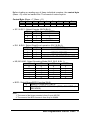
1
NuIPC / NuDAQ cPCI-7300A / PCI-7300A 80MB Ultra-High Speed 32-CH Digital I/O Boards User’s Guide @Copyright 1998~2000 ADLINK Technology Inc. All Rights Reserved. Manual Rev 2.20: August 24, 2000 The information in this document is subject to change without prior notice in order to improve reliability, design and function and does not represent a commitment on the part of the manufacturer. In no event will the manufacturer be liable for direct, indirect, special, incidental, or consequential damages arising out of the use or inability to use the product or documentation, even if advised of the possibility of such damages. This document contains proprietary information protected by copyright. All rights are reserved. No part of this manual may be reproduced by any mechanical, electronic, or other means in any form without prior written permission of the manufacturer. Trademarks NuDAQ , NuIPC , DAQBench are registered trademarks of ADLINK Technology Inc., Other product names mentioned herein are used for identification purposes only and may be trademarks and/or registered trademarks of their respective companies. Getting service from ADLINK Customer Satisfaction is always the most important thing for ADLINK Tech Inc. If you need any help or service, please contact us and get it. ADLINK Technology Inc. Web Site Sales & Service Technical Support TEL Address http://www.adlink.com.tw [email protected] NuDAQ [email protected] NuDAM [email protected] NuIPC [email protected] NuPRO [email protected] Software [email protected] AMB [email protected] +886-2-82265877 FAX +886-2-82265717 9F, No. 166, Jian Yi Road, Chungho City, Taipei, 235 Taiwan, R.O.C. Please inform or FAX us of your detailed information for a prompt, satisfactory and constant service. Detailed Company Information Company/Organization Contact Person E-mail Address Address Country TEL Web Site FAX Questions Product Model Environment to Use OS Computer Brand M/B: CPU: Chipset: Bios: Video Card: Network Interface Card: Other: Challenge Description Suggestions for ADLINK Contents Chapter 1 Introduction ........................................................... 1 1.1 1.2 1.3 1.4 APPLICATIONS .........................................................................................2 FEATURES .................................................................................................2 SPECIFICATIONS .....................................................................................3 SOFTWARE SUPPORTING....................................................................4 1.4.1 P R O G R A M M I N G L I B R A R Y ........................................................ 5 1.4.2 P C I S -L V I E W : L A B V I E W D R I V E R ............................................ 5 1.4.3 P C I S -VEE: HP -V E E D R I V E R ...................................................... 5 1.4.4 DAQBENCH ® TM : A C T I V E X C O N T R O L S .................................... 6 Chapter 2 Installation ............................................................. 7 2.1 2.2 2.3 2.4 2.5 2.6 2.7 2.8 WHAT YOU HAVE....................................................................................7 UNPACKING..............................................................................................8 DEVICE INSTALLATION FOR WINDOWS SYSTEMS ......................8 PCI-7300A'S LAYOUT .............................................................................9 HARDWARE INSTALLATION OUTLINE ...........................................11 CONNECTOR PIN ASSIGNMENT .......................................................12 WIRING AND TERMINATION..............................................................14 DAUGHTER BOARD SUPPORTING .................................................15 2.8.1 C O N N E C T W I T H D I N -1 0 0 S ....................................................... 15 2.8.2 C O N N E C T W I T H D I N -5 0 2 S ....................................................... 15 Chapter 3 Registers Format ................................................ 16 3.1 3.2 3.3 3.4 3.5 3.6 3.7 3.8 3.9 I/O PORT BASE ADDRESS ..................................................................17 DI_CSR: DI CONTROL & STATUS REGISTER................................18 DO_CSR: DO CONTROL & STATUS REGISTER............................19 AUXILIARY DIGITAL I/O REGISTER..................................................21 INT_CSR: INTERRUPT CONTROL AND STATUS REGISTER.....21 DI_FIFO: DI FIFO DIRECT ACCESS PORT ......................................22 DO_FIFO: DO EXTERNAL DATA FIFO DIRECT ACCESS PORT23 FIFO_CR: FIFO ALMOST EMPTY/FULL REGISTER ......................24 POL_CNTRL: CONTROL SIGNAL POLARITY CONTROL REGISTER ................................................................................................24 3.10 PLX PCI-9080 DMA CONTROL REGISTERS ..................................25 Contents · i Chapter 4 Operation Theorem............................................. 26 4.1 I/O CONFIGURATION............................................................................26 4.2 BLOCK DIAGRAM ..................................................................................27 4.3 DIGITAL I/O DATA FLOW .....................................................................28 4.4 INPUT FIFO AND OUTPUT FIFO .........................................................29 4.5 BUS-MASTERING DMA ........................................................................30 4.6 SCATTER/GATHER DMA .....................................................................31 4.7 CLOCKING MODE..................................................................................32 4.8 STARTING MODE...................................................................................33 4.9 ACTIVE TERMINATOR ..........................................................................34 4.10 DIGITAL INPUT OPERATION MODE................................................34 4.10.1 D I G I T A L I N P U T D M A I N I N T E R N A L C L O C K M O D E .......... 34 4.10.2 D I G I T A L I N P U T D M A I N E X T E R N A L C L O C K M O D E ......... 36 4.10.3 D I G I T A L I N P U T D M A I N H A N D S H A K I N G M O D E ................ 38 4.10.4 C O N T I N U O U S D I G I T A L I NPUT ............................................... 40 4.11 DIGITAL OUTPUT OPERATION MODE............................................41 4.11.1 D I G I T A L O U T P U T D M A I N I N T E R N A L C L O C K M O DE ...... 41 4.11.2 D I G I T A L O U T P U T D M A I N H A N D S H A K I N G M O D E ........... 42 4.11.3 DIGITAL OUTPUT DMA IN BURST HANDSHAKING MODE 4.11.4 P A T T E R N G E N E R A T O R ........................................................... 45 ........................................................................................................ 44 4.12 AUXILIARY DIO .....................................................................................46 Chapter 5 C/C++ Libraries.................................................... 47 5.1 LIBRARIES INSTALLATION ................................................................47 5.2 PROGRAMMING GUIDE .......................................................................48 5.2.1 N A M I N G C O N V E N T I O N ............................................................ 48 5.2.2 D A T A T Y P E S ............................................................................... 48 5.3 _7300_INITIAL .........................................................................................49 5.4 _7300_CLOSE .........................................................................................50 5.5 _7300_CONFIGURE...............................................................................50 5.6 _7300_DI_MODE.....................................................................................52 5.7 _7300_DO_MODE...................................................................................53 5.8 _7300_AUX_DI ........................................................................................54 5.9 _7300_AUX_DI_CHANNEL ...................................................................54 5.10 _7300_AUX_DO .....................................................................................55 5.11 _7300_AUX_DO_CHANNEL ...............................................................55 5.12 _7300_ALLOC_DMA_MEM .................................................................56 ii · Contents 5.13 5.14 5.15 5.16 5.17 5.18 5.19 5.20 5.21 5.22 5.23 5.24 5.25 5.26 5.27 5.28 _7300_FREE_DMA_MEM ....................................................................57 _7300_DI_DMA_START .......................................................................57 _7300_DI_DMA_STATUS ....................................................................60 _7300_DI_DMA_ABORT......................................................................60 _7300_GETOVERRUNSTATUS ..........................................................61 _7300_DO_DMA_START .....................................................................61 _7300_DO_DMA_STATUS ..................................................................63 _7300_DO_DMA_ABORT....................................................................63 _7300_DO_PG_START ........................................................................64 _7300_DO_PG_STOP...........................................................................65 _7300_DI_TIMER ...................................................................................65 _7300_DO_TIMER .................................................................................66 _7300_INT_TIMER.................................................................................66 _7300_GET_SAMPLE...........................................................................67 _7300_SET_SAMPLE...........................................................................68 _7300_GETUNDERRUNSTATUS .......................................................68 Appendix A 8254 Programmable Interval Timer ............... 70 A.1 THE INTEL (NEC) 8254 .........................................................................70 A.2 THE CONTROL BYTE............................................................................70 A.3 MODE DEFINITION.................................................................................72 Product Warranty/Service ..................................................... 74 Contents · iii How to Use This Manual This manual is designed to help you use the cPCI-7300 and PCI-7300A Rev.B. The manual describes how to modify various settings on the PCI-7300A card to meet your requirements. It is divided into five chapters: Ø Chapter 1, "Introduction", gives an overview of the product applications, and specifications. features, Ø Chapter 2, "Installation", describes how to install the PCI-7300A. The layout of PCI-7300A is shown, and the installation procedures, pin assignment of connectors, and timer pacer generation are specified. Ø Chapter 3, "Register Structure & Format", describes the low-level register structure and format of the PCI-7300A. Ø Chapter 4, "Operation Theorem", describes how to use the operations of digital input and output on the PCI-7300A. Ø Chapter 5, "C/C++ & DLL Library", describes the high level C and DLL library functions. It will help you to programming in DOS, Win 3.11, Win-95 and Win-NT environments. Ø Appendix A, "8254 Programmable Interval Timer“, describes the detailed structure and register format of 8254 timer/counter chip. 1 Introduction The cPCI/PCI-7300A is cPCI/PCI form factor ultra-high speed digital I/O card, it consists of 32 digital input or output channel. High performance designs and the state-of-the-art technology make this card to be ideal for high s peed digital input and output applications. The cPCI/PCI-7300A performs high-speed data transfers using bus mastering DMA and scatter/gather via 32-bit PCI bus architecture. The maximum data transfer rates can be up to 80MB per second. It is very suitable for interface between high speed peripherals and your computer system. The cPCI/PCI-7300A is configured as two ports, PORTA and PORTB, each port controls 16 digital I/O lines. The I/O can configure as either input or output, and 8-bit or 16-bit. According to outside device environment, users can configure cPCI/PCI-7300A to meet all high speed digital I/O data transfer. There are 4 different digital I/O operation modes are supported: 1. Internal Clock: the digital input and output operations are paced by internal clock and transferred by bus mastering DMA. 2. External Clock: the digital input operation is paced by external strobe signal ( DIREQ ) and transferred by bus mastering DMA. 3. Handshaking: through REQ signal and ACK signal, the digital I/O data can have simple handshaking data transfer. 4. Pattern Generation: You can output a digital pattern repeatedly at a predetermined rate. The transfer rate is controlled by internal timer. Introduction · 1 1.1 Applications Ø Interface to high-speed peripherals Ø High-speed data transfers from other computers Ø Automated test equipment (ATE) Ø Electronic and logic testing Ø Interface to external high-speed A/D and D/A converter Ø Digital pattern generator Ø Waveform and pulse generation Ø Parallel digital communication 1.2 Features The PCI-7300A Ultra-High Speed DIO card provides the following advanced features: Ø 32 digital input/output channels Ø Extra 4-bit TTL digital input and output channels Ø Transfer up to 80M Bytes per second Ø SCSI active terminator for high speed and long distance data transfer Ø 32-bit PCI bus Ø Plug and Play Ø Scatter/gatter DMA Ø On-board internal clock generator Ø Internal timer/external clock controls input sampling rate Ø Internal timer control digital output rate Ø ACK and REQ for handshaking Ø TRIG signal controls start of data acquisition/pattern generation Ø On-board 64KB FIFO Ø 100-pin SCSI style connector 2 · Introduction 1.3 Specifications Ø Digital I/O (DIO) l Numbers of Channel: 32 TTL compatible inputs and/or outputs l Device: IDT 74FCT373 l I/O Configurations: l ♦ 16 DI & 16 DO ♦ 32 DI ♦ 32 DO Input Voltage: l Low: Min. 0V; Max. 0.8V High: Min. +2.0V Input Load: l Terminator OFF: Low: +0.5V @ ±20 mA High: +2.7V @ ±1 mA max. Terminator ON: Termination resistor: 110 Ohms Termination voltage: 2.9V Low: +0.5V @ ±22.4mA High: +2.7V @ ± 1mA max. Output Voltage: l Low: Min. 0V; Max. 0.5V High: Min. +2.7V Driving Capacity: l Low: Max. +0.5V at 48mA (Sink) High: Min. 2.4V at -8 mA (Source) Hysteresis: 500mV Ø Transfer Characteristic l Mode: Bus Mastering DMA with Scatter/Gather l Data Transfers: 8/16/32-bit input or output (programmable) l DMA Transfer count: 2M double words (8M bytes) for non-chaining mode DMA No limitation for chaining mode (scatter/gather) DMA Introduction · 3 l Max. Transfer rate: DO: 80M Bytes/sec: 32-bit output @ 20 MHz DI: 80M Bytes/sec: 32-bit input @ 20 MHz Ø Programmable Counter l Device: 82C54-10 l Digital Input Pacer: 20MHz, 10MHz, or clock output of Timer #0 l Digital Output Pacer: 20MHz, 10MHz, or clock output of Timer #1 l General Purpose Timer: Output of Timer #2 Ø General Specifications l Connector: one 100-pin male SCSI-II style cable connector l Operating Temperature: 0° C ~ 60°C l Storage Temperature: -20° C ~ 80°C l Humidity: 5 ~ 95%, non-condensing l Dimension: Compact size only 179mm(L) X 102mm(H) l Power Consumption: +5 V @ 830 mA max. with on-board terminator off or +5 V @ 1.0A max. with on-board terminator on 1.4 Software Supporting ADLink provides versatile software drivers and packages for users’ different approach to built-up a system. We not only provide programming library such as DLL for many Windows systems, but also provide drivers for software ® TM TM TM packages such as LabVIEW , HP VEE , DASYLab , InTouch , TM TM InControl , ISaGRAF , and so on. All the software options are included in the ADLink CD. The non-free software drivers are protected with serial licensed code. Without the software serial number, you can still install them and run the demo version for two hours for demonstration purpose. Please contact with your dealer to purchase the formal license serial code. 4 · Introduction 1.4.1 Programming Library For customers who are writing their own programs, we provide function libraries for many different operating systems, including: u DOS Library: Borland C/C++ and Microsoft C++, the functions descriptions are included in this user’s guide. u Windows 95 DLL: For VB, VC++, Delphi, BC5, the functions descriptions are included in this user’s guide. u PCIS-DASK: Include device drivers and DLL for Windows 98, Windows NT and Windows 2000. DLL is binary compatible across Windows 98, Windows NT and Windows 2000. That means all applications developed with PCIS-DASK are compatible across Windows 98, Windows NT and Windows 2000. The developing environment can be VB, VC++, Delphi, BC5, or any Windows programming language that allows calls to a DLL. The user’s guide and function reference manual of PCIS-DASK are in the CD. Please refer the PDF manual files under \\Manual_PDF\Software\PCIS-DASK The above software drivers are shipped with the board. Please refer to the “Software Installation Guide” to install these drivers. 1.4.2 ® PCIS-LVIEW: LabVIEW Driver ® PCIS-LVIEW contains the VIs, which are used to interface with NI’s LabVIEW software package. The PCIS-LVIEW supports Windows 95/98/NT/2000. The ® LabVIEW drivers are free shipped with the board. You can install and use them without license. For detail information about PCIS-LVIEW, please refer to the user’s guide in the CD. (\\Manual_PDF\Software\PCIS-LVIEW) 1.4.3 PCIS-VEE: HP-VEE Driver The PCIS-VEE includes the user objects, which are used to interface with HP VEE software package. PCIS-VEE supports Windows 95/98/NT. The HP-VEE drivers are free shipped with the board. You can install and use them without license. For detail information about PCIS-VEE, please refer to the user’s guide in the CD. (\\Manual_PDF\Software\PCIS-VEE) Introduction · 5 1.4.4 TM DAQBench : ActiveX Controls We suggest the customers who are familiar with ActiveX controls and TM VB/VC++ programming use the DAQBench ActiveX Control components TM library for developing applications. The DAQBench is designed under Windows NT/98. For more detailed information about DAQBench, please refer to the user’s guide in the CD. (\\Manual_PDF\Software\DAQBench\DAQBench Manual.PDF) 6 · Introduction 2 Installation This chapter describes how to install the cPCI/PCI-7300A. At first, the contents in the package and unpacking information that you should be careful are described. Because the PCI-7300A is following the PCI design philosophy, it is no more jumpers and DIP switches setting for configuration. The Interrupt and I/O port address are the variables associated with automatic configuration, the resource allocation is managed by the system BIOS. Upon system power-on, the internal configuration registers on the board interact with the BIOS. 2.1 What You Have In addition to this User's Manual, the package includes the following items: Ø cPCI/PCI-7300A 80MB Ultra-High Speed 32-CH Digital I/O Card Ø ADLINK All-in-one CD Ø Software Installation Guide If any of these items is missing or damaged, contact the dealer from whom you purchased the product. Save the shipping materials and carton in case you want to ship or store the product in the future. Installation · 7 2.2 Unpacking Your cPCI/PCI-7300A card contains sensitive electronic components that can be easily damaged by static electricity. The card should be done on a grounded anti-static mat. The operator should be wearing an anti-static wristband, grounded at the same point as the anti-static mat. Inspect the card module carton for obvious damage. Shipping and handling may cause damage to your module. Be sure there are no shipping and handling damages on the module before processing. After opening the card module carton, extract the system module and place it only on a grounded anti-static surface component side up. Again inspect the module for damage. Press down on all the socketed IC's to make sure that they are properly seated. Do this only with the module place on a firm flat surface. Note: DO NOT APPLY POWER TO THE CARD IF IT HAS BEEN DAMAGED. You are now ready to install your cPCI/PCI-7300A. 2.3 Device Installation for Windows Systems Once Windows 95/98/2000 has started, the Plug and Play function of Windows system will find the new NuDAQ/NuIPC cards. If this is the first time to install NuDAQ/NuIPC cards in your Windows system , you will be informed to input the device information source. Please refer to the “Software Installation Guide ” for the steps of installing the device. 8 · Installation 2.4 PCI-7300A's Layout Figure 2.1 PCI-7300A Layout Diagram Installation · 9 Figure 2.2 cPCI-7300A Layout Diagram 10 · Installation 2.5 Hardware Installation Outline PCI configuration The PCI cards (or CompactPCI cards) are equipped with plug and play PCI controller, it can request base addresses and interrupt according to PCI standard. The system BIOS will install the system resource based on the PCI cards’ configuration registers and system parameters (which are set by system BIOS). Interrupt assignment and memory usage (I/O port locations) of the PCI cards can be assigned by system BIOS only. These system resource assignments are done on a board-by-board basis. It is not suggested to assign the system resource by any other methods. PCI slot selection Please note that the PCI slot must provide bus -mastering capability to operate this board well. Installation Procedures 1. Turn off your computer 2. Turn off all accessories (printer, modem, monitor, etc.) connected to your computer. 3. Remove the cover from your computer. 4. Select a 32-bit PCI slot. PCI slots are short than ISA or EISA slots, and are usually white or ivory. 5. Before handling the PCI cards, discharge any static buildup on your body by touching the metal case of the computer. Hold the edge and do not touch the components. 6. Position the board into the PCI slot you selected. 7. Secure the card in place at the rear panel of the system. Installation · 11 2.6 Connector Pin Assignment The PCI-7300A comes equipped with one 100-pin SCSI type connector (CN1) located on the rear mounting plate. The pin assignment of CN1 is illustrated in the figure 2.2. Legend: Pins Signal Name Signal Type Signal Direction 1…50 GND GND 51..66 PB15…PB0 DATA I/O 67 DOACK CONTR OL I 68 DOREQ CONTR OL O 69 DOTRIG CONTR OL I 70…73 AUXDO3…0 DATA O 85..100 PA15…PA0 DATA I/O 82 DIACK CONTR OL O 83 DIREQ CONTR OL I 12 · Installation Description Ground – these lines are the ground reference for all other signals PortB bidirectional data liness-PB15 is the MSB, and PB0 is the LSB. Digital output Acknowledge lines – In handshaking mode, DOACK carries handshaking status information from the peripheral. Request line – In handshaking mode, DOREQ carries handshaking control information to peripheral. DO TRIG- can be used to control the start of data output in all DO modes and to control the stop of pattern generation in pattern generation mode. AUX DO 3…0 – can be used as extra output data or can be used as extra control signals. PortA bidirectional data liness-PA15 is the MSB, and PA0 is the LSB. Digital output Acknowledge lines – In handshaking mode, DIACK carries handshaking status information to the peripheral. Request line – In handshaking mode, DIREQ carries handshaking control information from peripheral. In external clock mode, DIREQ carries the external clock input. 84 DITRIG CONTR OL I 78…81 AUXDI3…0 DATA I 74…77 TERMPWR POWER PA0 PA1 PA2 PA3 PA4 PA5 PA6 PA7 PA8 PA9 PA10 PA11 PA12 PA13 PA14 PA15 DI_TRG DI_REQ DI_ACK AUXI0 AUXI1 AUXI2 AUXI3 TERMPWR TERMPWR TERMPWR TERMPWR AUXO0 AUXO1 AUXO2 AUXO3 DO_TRG DO_REQ DO_ACK PB0 PB1 PB2 PB3 PB4 PB5 PB6 PB7 PB8 PB9 PB10 PB11 PB12 PB13 PB14 PB15 100 99 98 97 96 95 94 93 92 91 90 89 88 87 86 85 84 83 82 81 80 79 78 77 76 75 74 73 72 71 70 69 68 67 66 65 64 63 62 61 60 59 58 57 56 55 54 53 52 51 DI TRIG – can be used to control the start of data acquisition in all DI modes. AUX DI 3…0 – can be used as extra input data or can be used as extra control signals. TERMPWR -- 4.7V active terminator power output 50 49 48 47 46 45 44 43 42 41 40 39 38 37 36 35 34 33 32 31 30 29 28 27 26 25 24 23 22 21 20 19 18 17 16 15 14 13 12 11 10 9 8 7 6 5 4 3 2 1 GND GND GND GND GND GND GND GND GND GND GND GND GND GND GND GND GND GND GND GND GND GND GND GND GND GND GND GND GND GND GND GND GND GND GND GND GND GND GND GND GND GND GND GND GND GND GND GND GND GND Figure 2.2 CN1 Pin Assignment Installation · 13 2.7 Wiring and Termination Transmission line effects and environment noise, particularly on clock and control lines, can lead to incorrect data transfers if you do not take care when running signal wires to and from the devices. Take the following precautions to ensure a uniform transformation line and minimize noise pickup: 1. Use twisted-pair wires to connect digital I/O signals to the device. Twist each digital I/O signal with a GND line. In PCI-7300A, 50 signals are used as GND. 2. Place a shield around the wires connecting digital I/O signal to device. 3. Route signals to the devices carefully. Keep cabling away from noise sources, such as video monitor. For cPCI/PCI-7300A, it is important to terminate your cable properly to reduce or eliminate signal reflections in the cable. The PCI-7300A support active terminator on board, you can enable or disable the terminator by software selection. This is a good way to include termination on the signal transmission. Additional recommendations apply for all signal connection to your cPCI/PCI-7300A are listed as follows: 1. Separate cPCI/PCI-7300A device signal lines from high-current or high-voltage line. These lines are capable of inducing currents in or voltages on the cPCI/PCI-7300A if they run in parallel paths at a close distance. To reduce the magnetic coupling between lines, separate them by a reasonable distance if they run in parallel, or run the lines at right angles to each other. 2. Do not run signal lines through conducts that also contain power lines. 3. Protect signal lines from magnetic fields. 14 · Installation 2.8 Daughter Board Supporting The cPCI/PCI-7300A can be connected with two daughter boards: DIN-100S or DIN-502S. The functionality and connections are specified as follows. 2.8.1 Connect with DIN-100S The DIN-100S is a direct connection for the add-on card that is equipped with SCSI-100 connector. User can connect this daughter board by a 100-pin SCSI type cable (ACL-102100) to the cPCI/PCI-7300A. It is suitable for the applications of 32-bit digital input or 32-bit digital output. 2.8.2 Connect with DIN-502S The DIN-502S with the cable ACL-10252 separates the 100-pin SCSI connector into two 50-pin SCSI connectors. One 50 pin connector is for pin 1 ~ 25 and pin 51~75 of CN1 while the other one is for pin 26 ~ 50 and pin 76~100 of CN1. That means the DIN-502S and the ACL-10252 make users easy to connect the 16-bit digital inputs and 16-bit digital outputs by using two 50-pin daughter boards respectively. The independent wiring of 16-bit DI and 16-bit DO let users convenient to setup and maintain his systems. Installation · 15 3 Registers Format In this chapter, the registers’ format of the cPCI/PCI-7300A is described. Please note that the registers’ map of the PCI-7300A Rev.B is different from the PCI-7300A Rev.A This information is quite useful for the programmers who wish to handle the card by low-level programming. In addition, users can realize how to use software driver to manipulate this card after understanding the registers' structure of the cPCI/PCI-7300A The cPCI/PCI-7300A functions as a 32-bit PCI master device on the PCI bus. There are three types of registers on the cPCI/PCI-7300A: PCI Configuration Registers (PCR), Local Configuration Registers (LCR) and cPCI/PCI-7300A’s registers. The PCR, which compliant to the PCI-bus specifications, is initialized and controlled by the plug & play (PnP) PCI BIOS. User‘s can study the PCI BIOS specification to understand the operation of the PCR. Please contact with PCISIG to acquire the specifications of the PCI interface. The LCR is specified by the PCI bus controller PLX PCI-9080, which is provided by PLX technology Inc. (www.plxtech.com) . It is not necessary for users to understand the details of the LCR if you use the software library. The base address of the LCR is assigned by the PCI PnP BIOS. The assigned address is located at offset 14h of PCR. 16 · Registers Format 3.1 I/O Port Base Address The registers of the cPCI/PCI-7300A are shown in Table 3.1. The base address of these registers is also assigned by the PCI P&P BIOS. The assigned base address is stored at offset 18h of the PCR. Therefore, users can read the PCR to know the base address by using BIOS function call. Note that the cPCI/PCI-7300A registers are all 32 bits. Users should access these registers by 32 bits I/O instructions. The PCI-7300A occupies 8 consecutive 32-bit I/O addresses in the I/O address space. Table 3.1 shows the I/O Map of the PCI-7300A rev.B. Address Base + 0 Base + 4 Base + 8 Base + C Base + 10 Base + 14 Base + 18 Base + 1C Base + 20 Base + 24 Base + 28 Base + 2C Read DI_CSR DO_CSR AUX_DIO INT_CSR DI_FIFO DO_FIFO POL_CTRL 8254_COUNT0 8254_COUNT1 8254_COUNT2 8254_CONTROL Write DI_CSR DO_CSR AUX_DIO INT_CSR DI_FIFO DO_FIFO FIFO_CR POL_CTRL 8254_COUNT0 8254_COUNT1 8254_COUNT2 8254_CONTROL Legend: DI_CSR: Digital input control & status register DO_SCR: Digital output control & status register AUX_DIO: Auxiliary digital I/O port INT_CSR: Interrupt control and status register DI_FIFO: DI FIFO direct access port DO_FIFO: DO FIFO direct access port FIFO_CR: FIFO almost empty/full programming register POL_CTRL: Polarity control register for the control signals Caution: 1. I/O port is 32-bit width 2. 8-bit or 16-bit I/O access is not allowed. Registers Format · 17 3.2 DI_CSR: DI Control & Status Register Digital input control and status checking is done by this register. Address: BASE + 00 Attribute: READ/WRITE Data Format: Bit # 3~0 DI_HND_SHK Bit # 7~4 0 Bit # 11~8 Bit # 15~12 Bit # 31~16 DI_FIFO_FULL Don’t Cared DI_CLK_SEL PA_TERM_OF DI_WAIT_TRI F G DI_OVER DI_FIFO_CLR - DI_32 -- (1) DI_EN DI-FIFO_EMPTY (1) This bit is different between Rev.A and Rev.B. DI_32 (R/W) 0: Input port is not 32-bit wide (16-bit or 8-bit wide) 1: Input port is 32-bit wide, PORTB is configured as the extension of PORTA. That means PORTA is input lines 0…15, and PORTB is input lines 16…31. All the PORTB control signals are disabled. DI_CLK_SEL (R/W) 00: use timer0 output as input clock 01: use 20MHz clock as input clock 10: use 10MHz clock as input clock 11: use external clock (DI_REQ) as input clock DI_HND_SHK (R/W) 0: No handshaking 1: REQ/ACK handshaking mode DI_WAIT_TRIG (R/W) 0: delay input sampling until DITRIG is active 1: start input sampling immediately PA_TERM_OFF (R/W) 0: PORTA terminator ON 1: PORTA terminator OFF DI_EN (R/W) 0: Disable digital inputs 1: Enable digital inputs 18 · Registers Format DI_FIFO_CLR (R/W) 0: No effect 1: Clear digital input FIFO. If both PORTA and PORTB are configured as inputs, both FIFO will be cleared. Always get 0 when read. DI_OVER (R/W) 0: DI FIFO does not full during input sampling 1: DI FIFO full during input sampling, some input data was lost, write “1” to clear this bit DI_FIFO_FULL (RO) 0: DI FIFO is not full 1: DI FIFO is full DI_FIFO_EMPTY (RO) 0: DI FIFO is not empty 1: DI FIFO is empty 3.3 DO_CSR: DO Control & Status Register Digital input control and status checking is done by this register. Address: BASE + 04 Attribute: READ/WRITE Data Format: Bit # 3~0 Bit # 7~4 Bit # 11~8 Bit # 15~12 Bit # 31~16 DO_WAIT_NAE DO_MODE PG_STOP_TRIG PB_TERM_OFF DO_WAIT_TRG DO_32 PAT_GEN DO_FIFO_FULL DO_UNDER DO_FIFO_CLR DO_EN - - BURST_HNDSH (2) DO_FIFO_EMPTY Don’t Cared (2) This bit is different between Rev.A and Rev.B. DO_32 (R/W) 0: Output port is not 32-bit wide ( 16-bit or 8-bit wide) 1: Output port is 32-bit wide, PORTA is configured as the extension of PORTB. That means PORTB is output lines (0…15), and PORTA is output lines (16…31). All PORTA control signals are disabled. DO_MODE (R/W) 00: use timer1 output as output clock 01: use 20MHz clock as output clock 10: use 10MHz clock as output clock 11: REQ/ACK handshaking mode Registers Format · 19 DO_WAIT_NAE (R/W) 0: do not wait output FIFO not almost empty flag 1: delay output data until FIFO is not almost empty PAT_GEN(R/W) 0: pattern generation disable (FIFO data do not repeat during data output) 1: pattern generation enable (FIFO data repeat themselves during data output) DO_WAIT_TRIG (R/W) 0: delay output data until DOTRIG is actived 1: start output data immediately PB_TERM_OFF (R/W) 0: PORTB terminator ON 1: PORTB terminator OFF PG_STOP_TRIG (R/W) 0: no effect 1: Stop pattern generation when DOTRIG is deasserted DO_EN (R/W) 0: Disable digital outputs 1: Enabled digital outputs DO_FIFO_CLR (R/W) 0: No effect 1: Clear digital output FIFO. If both PORTA and PORTB are configured as outputs, both FIFO will be cleared. Always get 0 when read. DI_UNDER (R/W) 0: DO FIFO does not empty during data output 1: DO FIFO is empty during data output, some output data may be output twice. Write 1 to clear this bit DO_FIFO_FULL (RO) 0: DO FIFO is not full 1: DI FIFO is full DO_FIFO_EMPTY (RO) 0: DO FIFO is not empty 1: DO FIFO is empty 20 · Registers Format BURST_HNDSHK (R/W) 0: disable burst handshaking mode 1: enable burst handshake mode * Note: This bit is for Rev.B only. 3.4 Auxiliary Digital I/O Register Auxiliary 4-bit digital inputs and 4 -bit digital outputs Address: BASE + 08 Attribute: READ/WRITE Data Format: Bit # 3~0 DO_AUX_3 DO_AUX_2 Bit # 7~4 DI_AUX_3 DI_AUX_2 Bit # 31~8 Don’t Cared DO_AUX_1 DI_AUX_1 DO_AUX_0 DI_AUX_0 This auxiliary digital I/O is controlled by porgram I/O only. DO_AUX_3 ~ DO_AUX_0 (R/W) 4-bit auxiliary output port. Program I/O only. DI_AUX_3 ~ DI_AUX_0 (R) 4-bit auxiliary input port. Program I/O only 3.5 INT_CSR: Interrupt Control and Status Register The interrupt of PCI-7300A is controlled and status is checked through this register. Address: BASE + 0x0C Attribute: READ/WRITE Data Format: Bit # 3~0 Bit # 7~4 Bit # 31~8 T2_INT Don’t Cared AUXIO_INT - T2_EN Reserved AUXDI0_EN Reserved AUXDI_EN (R/W) 0: Disable AUXDI0 interrupt 1: Interrupt CPU on falling edge of AUXDI0 Registers Format · 21 T2_EN (R/W) 0: Disable Timer2 interrupt 1: Interrupt CPU on falling edge of Timer 2 output AUXDI0_INT (R/W) 0: AUXDI does not generate interrupt 1: AUXDI interrupt occurred. Write “1” to clear T2_EN (R/W) 0: Timer 2 does not generate interrupt 1: Timer 2 interrupt occurred. Write “1” to clear 3.6 DI_FIFO: DI FIFO direct access port The digital input FIFO data can be accessed through this port directly. Address: BASE + 0x10 Attribute: READ/WRITE Data Format: Bits Bit # 7~0 Bit # 15~8 Bit # 31_16 7 6 5 4 3 2 1 0 DI_FIFO_8 DI_FIFO_16 DI_FIFO_32 DI_FIFO_8 Bit 7 ~ Bit 0 of digital input FIFO DI_FIFO_16 Bit 15 ~ Bit 8 of digital input FIFO if the digital input is configured as 16-bit wide or 32-bit wide. DI_FIFO_32 Bit 31 ~ Bit 16 of digital input FIFO if the digital input is configured as 32-bit wide Note: Although this port is R/W port, write operation should be avoided in normal operation. If both PORT A and PORT B are configured as output ports, read/write to this port is meaningless. 22 · Registers Format 3.7 DO_FIFO: DO external data FIFO direct access port The digital output FIFO data can be accessed through this port directly. Address: BASE + 0x0C Attribute: READ/WRITE Data Format: Bits 7 6 Bit # 7~0 Bit # 15~8 Bit # 31_16 DO_FIFO_8 DO_FIFO_16 DO_FIFO_32 5 4 3 2 1 0 DO_FIFO_8 Bit 7 ~ Bit 0 of digital output FIFO DO_FIFO_16 Bit 15 ~ Bit 8 of digital output FIFO if the digital output is configured as 16-bit wide or 32-bit wide. DO_FIFO_32 Bit 31 ~ Bit 16 of digital output FIFO of the digital output is configured as 32-bit wide Note: Although this port is R/W port, read operation should be avoided in normal operation. If both PORTA and PORTB are configured as input ports, read/write to this port is meaningless. Registers Format · 23 3.8 FIFO_CR: FIFO almost empty/full register The register is used to control the FIFO programmable almost empty/full flag. Address: BASE + 0x018 Attribute: WRITE Only Data Format: Bits Bit 15~0 Bit 31_16 7 6 5 PB_PAE_PAF PA_PAE_PAF 4 3 2 1 0 PB_PAE_PAF (WO) Programmable almost empty/full threshold of PORTB FIFO, 2 consecutive writes are required to program PORTB FIFO. Programmable almost empty threshold first. PA_PAE_PAF(WO) Programmable almost empty/full threshold of PORTA FIFO, 2 consecutive writes are required to program PORTA FIFO. Programmable almost empty threshold first. 3.9 POL_CNTRL: Control Signal Polarity Control Register The register is used to control the control signals’ polarity. The control signals include DI_REQ, DI_ACK, DI_TRG, DO_REQ, DO_ACK and DO_TRG. Please note that this register is for PCI-7300A Rev.B and cPCI-7300 only. Address: BASE + 0x1C Attribute: READ/WRITE Data Format: Bit # 3~0 DO_REG_NEG DI_TRG_NEG DI_ACK_NEG DI_REQ_NEG Bit # 71~4 - - DO_TRG_NEG DO_ACK_NEG Bit # 31~8 Don’t Cared DI_REQ_NEQ (R/W) 0: DI_REQ is rising edge active 1: DI_REQ is falling edge active 24 · Registers Format DI_ACK_NEQ (R/W) 0: DI_ACK is rising edge active 1: DI_ACK is falling edge active DI_TRG_NEQ (R/W) 0: DI_TRG is rising edge active 1: DI_TRG is falling edge active DO_REQ_NEQ (R/W) 0: DO_REQ is rising edge active 1: DO_REQ is falling edge active DO_ACK_NEQ (R/W) 0: DO_ACK is rising edge active 1: DO_ACK is falling edge active DO_TRG_NEQ (R/W) 0: DO_TRG is rising edge active 1: DO_TRG is falling edge active 3.10 PLX PCI-9080 DMA Control Registers The registers of bus -mastering DMA as well as the control and status registers of PCI-bus interrupts are built in the PLX PCI-9080 ASIC. Users can refer to the manual of PLX PCI-9080 for detailed information. Registers Format · 25 4 Operation Theorem This chapter provides the detailed operation information for the cPCI/PCI-7300A, including I/O configuration, block diagram, input/output FIFO, bus -mastering DMA, scatter/gather, clocking mode, starting mode, termination, I/O transfer mode, and auxiliary digital I/O. 4.1 I/O Configuration The 32-bit I/O data path of PCI-7300A can be configured as 8-bit, 16-bit, or 32-bit, the possible configuration modes are listed as follows. Mode DI32 DO32 DI16DO16 (default mode) DI16DO8 DI8DO16 DI8DO8 26 · Operation Theorem Channel Description PORTA (DI0…DI15) Both PORTA and PORTB PORTB (DI16..DI31) are configured as input channel PORTA Both PORTA and PORTB (DO16…DO31) are configured as output PORTB channel (DO0…DO15) PORTA (DI0…DI15) PORTA is 16-CH input PORTB PORTB is 16-CH output (DO0…DO15) PORTA (DI0…DI15) PORTA is 16-CH input PORTB (DO0…DO7) PORTB is 8-CH output PORTA (DI0…DI7) PORTA is 8-CH input PORTB PORTB is 16-CH output (DO0…DO15) PORTA (DI0…DI7) PORTA is 8-CH input PORTB (DO0…DO7) PORTB is 8-CH output Notes: PORTA is default as Input channel; PORTB is default as output channel. In DI32 mode, the PORTB has to be configured as the extension of PORTA, that is, PORTB is the input port (DI16…DI31). PORTB control signals are disabled. In DO32 mode, the PORTA has to be configured as the extension of PORTB, that is, PORTA is the output port (DO16…DO31). PORTA control signals are disabled. DI0: input LSB, DI31: input MSB; DO0:output LSB, DO31:output MSB. LSB: Least Significant Bit, MSB: Most Significant Bit 4.2 Block Diagram Figure 4.1 shows the block diagram of the cPCI/PCI-7300A, it includes the I/O registers, two 16K FIFOs, auxiliary DIO, active terminators, and so on. Figure 4.1: Block diagram PORTA: PORTB: FIFO: AUX DO 3..0: AUX DI 3..0: 16 Digital I/O Port, it can be set as terminated mode or non-terminated mode 16 Digital I/O Port, it can be set as terminated mode or non-terminated mode Two 16K words FIFO for digital I/O data buffer Four auxiliary digital outputs Four auxiliary digital inputs Operation Theorem · 27 DITRIG: Digital input trigger line DIACK/DIREQ: Digital input handshaking signals DOTRIG: Digital output trigger line DOACK/DOREQ:Digital output handshaking signals 4.3 Digital I/O Data Flow When applying digital input functions, the data will be sampled into the input FIFO periodically as we configured and then transfer to the system memory by the bus mastering DMA of the PCI Bridge. Figure 4.2 show the data flow of the 16-bit digital input operation. Figure 4.2 Data flow of digital input On the other hand, Figure 4.3 shows the data flow of 16-bit digital output operation. After the bus mastering DMA of the PCI Bridge transfers the output data to the output FIFO, the cPCI/PCI-7300A will output the data to the external devices in a pre-assigned period. Figure 4.3 Data flow of digital output The width of local data bus on the cPCI/PCI-7300A can be programmable to be 8-bit, 16-bit or 32-bit. The default data width is 16-bit. Port A is default to be input port, and Port B is default to be output one. When 8-bit data width is applied, only the lower byte of the bus will be used. While we program the data width to be 32-bit, the two ports will operate in the same manner. 28 · Operation Theorem 4.4 Input FIFO and Output FIFO Due to the data transfer rate between external devices and the cPCI/PCI-7300A is independent from that between cPCI/PCI-7300A and PCI bus. Two 16K words FIFO are provided to be I/O buffers. For digital input operation, data is sampled and transferred to the input FIFO. When the input FIFO is non-empty, the PCI bridge will automatically transfer the data from the input FIFO to the system memory in the background when PCI bus is available. As the data transfer rate from external device to input FIFO (DI pre-transfer rate) is lower than that from input FIFO to system memory (DI post-transfer rate), the input FIFO is usually empty. On the contrary, when DI pre-transfer rate is higher than DI post-transfer rate, the FIFO becomes full and the overrun situation occurs if the data size is larger than the FIFO size, that is 16K samples. When DI overrun happens, the next input data will lose until the input FIFO becomes non-full once again. Users can check the overrun status by using the function _7300_GetOverrunStatus. For digital output operation, data is moved from system memory to the output FIFO by bus mastering DMA, assume the data transfer rate is DO pre-transfer rate. Then, the data will be transferred to the external devices periodically as we configured, assume the transfer rate is DO post-transfer rate. When the DO pre-transfer rate is higher than the DO post-transfer rate, the DMA transfer stops as the output FIFO becomes full. On the contrary, if DO pre-transfer rate is lower than DO post-transfer rate. The underrun situation occurs as the output FIFO becomes empty. The output data remains when underrun happens. User can check the underrun status by using the function _7300_GetUnderrunStatus. Notes: The max data length should be 16K instead of 32K. Users can send repetitive pattern of 8-/16-/32-bit width with a length of 16K samples, because of the FIFO depth is as it is no matter how wide the bus. Users should remember that the FIFO chip size is 32K bytes with 16-bits width. Therefore, for each bit, the depth is 16K. If you need more depth of data, the data have to be in the PC memory and chain the pattern memory circularly, and then do chaining mode DMA which will generate the desired pattern repetitively. Operation Theorem · 29 4.5 Bus-mastering DMA Digital I/O data transfer between PCI-7300A and PC’s system memory is through bus mastering DMA, which is controlled by PCI bridge chip PLX PCI-9080. The PCI bus master means the device requires fast access to the bus or high data throughput in order to achieve good performance. However, users should note that when more than one bus masters request the bus ownership, all masters will share the bandwidth of PCI bus and the performance of each master will unavoidably drop. Therefore, in order to obtain the maximum data throughput of the cPCI/PCI-7300A, it is recommended to remove or disable the bus mastering function of other bus masters, such as network, SCSI, modem adapters, and so on. The maximum data throughput of the cPCI/PCI-7300A is also limited by the data throughput of the bridge chipset (North Bridge: NB) between PCI bus and system memory. The typical data throughput of NB chipset is 120MB/s for input and 100MB/s for output. Please refer to the figure 4.6. User should check the specs of the chipset on your main-board to determine the cPCI/PCI-7300A‘s maximum data throughput. The 80MB/s data throughput of the cPCI/PCI-7300A is guaranteed in the pervious system setup by using the internal 20MHz-sampling rate. Figure 4.6: Maximum data throughput From figure 4.6, we can find that NB chipset is the bottleneck of the maximum data transfer rate as only one bus master exists. When the transfer rate users required is smaller than the maximum transfer rate, by using scatter/gather (see 4.6), users can transfer the maximum data size as they have on their system memory. However, if the data should be real-time saved to the hard-disk rather than memory, the bottleneck would be the data transfer rate of the hard-disk driver. 30 · Operation Theorem 4.6 Scatter/gather DMA The PCI Bridge also supports the function of scatter/gather bus mastering DMA, which helps the users to transfer a large amount of data by linking the all memory blocks into a continuous linked list. In the multi-user or multi-tasking OS, like Microsoft Windows, Linux, and so on. It is difficult to allocate a large continuous memory block to do the DMA transfer. Therefore, the PLX PCI-9080 provides the function of scatter/gather or chaining mode DMA to link the n on-continuous memory blocks into a linked list so that users can transfer a very large amount of data without limiting by the fragment of small size memory. Users can configure the linked list for the input DMA channel or the output DMA channel. The figure 4.7 shows the linked list that is constructed by three DMA descriptors. Each descriptor contains a PCI address, a local address, a transfer size, and the pointer to the next descriptor. Users can allocate many small size memory blocks and chain their associative DMA descriptors altogether by their application programs. The cPCI/PCI-7300A’s software driver provides the easy settings of the scatter/gather function, and some sample programs are also provided within the ADLink all-in-one CD. Users can refer to these sample programs and the function 5.14 and 5.18 for more detailed description. Figure 4.7: Scatter/gather DMA for digital output Operation Theorem · 31 In non-chaining mode, the maximum DMA data transfer size is 2M double words (8M bytes). However, by using chaining mode, scatter/gather, there is no limitation on DMA data transfer size. Users can also link the descriptor nodes circularly to achieve a double-buffered mode DMA. 4.7 Clocking Mode The data input to or output from the FIFO is operated in a specific rate. The specific sampling rate or the pacer rate can be programmable by software, by external clock, or by easy handshaking protocol. Four clocking modes are provided in the cPCI/PCI-7300A to sample input data to the FIFO or output date from FIFO to the external devices. They are: 1. Internal Clock : Three sources are available to activate both digital input and digital output. They are 20MHz, 10MHz, and programmable timer 82C54. There are three counters in 82C54, counter 0 is used to generate sampling clock for digital input, counter 1 is used timer pacer for digital output, and counter 2 is used for interrupt function. The configuration is illustrated as follows. Figure 4.8: Timer configuration 2. E x t e r n a l C l o c k: This mode is only applied for digital input. The digital inputs are handled by the external clock strobe (DI-REQ). The DI-ACK signal reflects the almost full status of the input FIFO. The DI-ACK is asserted when input FIFO is not almost full, which means the external device can input data. If the input FIFO is almost full, the DI-ACK is 32 · Operation Theorem de-asserted, then the external device should pause data transfer and wait for the assertion of DI-ACK. If the external device follows the rule, there would be no data lost due to FIFO overrun. 3. Handshaking: For the digital input, through DI-REQ input signal from external device and DI-ACK output signal to the external deviec, the digital input can have simple handshaking data transfer. For the digital output, through DO-REQ output signal to the dexternal device and DO-ACK input signal from external device, the digital output can have simple handshaking data transfer 4. Burst Handshaking: This mode is available for both digital output and digital input. If the digital output DMA use internal clock and the burst handshaking mode is enable, the cPCI/PCI-7300A output data only when DO-ACK is asserted. That is, the external device can control the data input from the cPCI/PCI-7300A by asserting the DO-ACK pin when it is ready to receive data. The software driver functions of 5.6 and 5.7 are provided to setup the clocking mode of digital input and digital output, respectively. Notes: Due to the internal clock is based on 10MHz clock, some specific sampling rate or pacer rate cannot be generated by software, such as 9MHz. For digital input, users can use the external clock source. However, for digital output, users should replace the default 40MHz oscillator because the current version of cPCI/PCI-7300A does not support external clock for digital output. The frequency of external input clock cannot exceed 40MHz due to the local bus timing requirement. When users replace the default oscillator on board, the corresponding frequency would be changed, for example, by replacement with 36Mhz oscillator, the internal clock selection would be changed to 18MHz, 9MHz, and 9MHz base timer output. 4.8 Starting Mode Users can also control the starting mode of digital input and output by external signals (DITRIG and DOTRIG) with the software programs. The trigger modes includes NoWait, WaitTRIG, WaitFIFO, and WaitBoth. 1. The data transfer is started immediately when a I/O transfer command is issued. NoWait: Operation Theorem · 33 The data transfer will not start until external trigger signal (DI-TRIG for digital input, DO-TRIG for digital output) is activated. 2. WaitTRIG: 3. WaitFIFO: 4. WaitBoth: This starting mode is only available for digital output. The data transfer is started until the output FIFO is not almost empty. The threshold of FIFO almost empty is software programmable. This starting mode is only available for digital output. The data transfer is started until the output FIFO is not almost empty and DO-TRIG signal is activated. The software driver functions of 5.6 and 5.7 are provided to setup the starting mode of digital input and digital output, respectively. 4.9 Active Terminator For cPCI/PCI-7300A, it is important to terminate your cable properly to reduce or eliminate signal reflections in the cable. The PCI-7300A support active terminator on board, you can enable or disable the terminator by software selection (Please refer to section 5.5 function _7300_config). The active terminator is the same as the one used in SCSI 2. When the terminator is ON, it presents a terminal 110-ohm impedance to the transmission line to match the line impedance. When it is OFF, it just add a few pF capacitance to the line 4.10 Digital Input Operation Mode 4.10.1 Digital Input DMA in Internal Clock Mode There are three sources to trigger digital input in the internal clock mode: 20MHz, 10MHz, and programmable timer 82C54. There are three counters in 82C54, where the counter 0 is used for sampling clock source for digital input. The operations sequence of digital input with internal clock are listed as follows: 1. Define the input configuration to be 32-bit, 16-bit or 8-bit data width. 2. Enable or disable the active terminators. 3. Define the input sampling rate to be 20MHz, 10MHz, or the output of 82C54 counter 0. 34 · Operation Theorem 4. Define the starting mode to be NoWait or WaitTRIG. 5. The digital input data are stored in the input FIFO after a DI command is issued and waiting for DI-TRIG signal if in WaitTRIG mode. 6. The data in the input FIFO will be transferred into system memory directly and automatically by bus mastering DMA. The operation flow is show as below: Operation Theorem · 35 Notes: When the DMA function of digital input starts, the input data will be stored in the FIFO of the cPCI/PCI-7300A. The data then transfer to system memory if PCI bus is available. If the speed of translation from external device to the FIFO on board is higher than that from FIFO to system memory or the PCI bus is busy for a long time, the FIFO become full and overrun situation occurs after the next data being written to the input FIFO. Users should check the overrun status to see whether the overrun occurs or not. Some input data will lost when the input FIFO is overrun. Notes: The overrun occurs when the DMA idle time (from the end of DMA transfer N to the start of DMA transfer N+1) is longer than the on-board FIFO buffer time. The FIFO size is 16K sample, so it has 1.6 ms buffer time for 10MHz sampling rate if the FIFO is empty when last DMA is complete. Users may try different DMA buffer size to see how the DMA buffer size affects the overall performance. Generally, the larger DMA size the less overhead, however, the process time required between DMAs also increases. 4.10.2 Digital Input DMA in External Clock Mode The digital input data transfer can be controlled by external strobe, which is from pin-83 DI-REQ of CN1. The operation sequence is very similar to Internal Clock. The only difference is the clock source comes from the outside peripheral devices. The operations sequence of digital input with external clock are listed: 1. Define the input configuration to be 32-bit, 16-bit or 8-bit data width. 2. Enable or disable the active terminators. 3. Define the input sampling rate as external clock. Connect the external clock to the input pin DI-REQ. 4. Define the starting mode to be NoWait or WaitTRIG. 5. The digital input data are stored in the input FIFO after a DI command is issued and waiting for DI-TRIG signal if in WaitTRIG mode.. 6. The data saved in FIFO will transfer to system memory of your computer directly and automatically by bus mastering DMA. 7. The DI-ACK signal indicates the status of the cPCI/PCI-7300A’s input FIFO is in external clock mode. When the digital input circuit of cPCI/PCI-7300A is enabled and its FIFO is not almost full, the DIACK signal will remain asserted. If the external device does not transfer data according to the status of DI-ACK, the on-board FIFO could be full and data could be lost. 36 · Operation Theorem The operation flow is show as below: The followings are timing diagrams of the DI-REQ and the input data. The active edge of DI-REQ can be programmed by the function 5.5. DIREQ as input data strobe (when Rising Edge Active) Operation Theorem · 37 DIREQ as input data strobe (when Falling Edge Active) Notes: From the timing diagram of external clock mode, the maximum frequency can be up to 40MHz. However, users should note that when the sampling frequency of digital input is higher than the PCI bus bandwidth (33Mhz), or the bandwidth of chipset (30Mhz typically) from PCI bus to system memory. Users should check the overrun status when the DMA block size is larger than 16K samples. If overrun always happens, users should reduce the DMA block size or slow down the sampling frequency. For example, the DMA block size should be smaller than 64K when the external clock is 40Mhz in the DOS Operation 4.10.3 Digital Input DMA in Handshaking Mode For digital input, through DI-REQ input signal and DI-ACK output signal, the digital input can have simple handshaking data transfer.The operations sequence of digital input with handshaking are listed: 1. Define the input configuration to be 32-bit, 16-bit or 8-bit data width. 2. Enable or disable the active terminators. 3. Define the input sampling rate as handshaking mode. Connect the handshaking signals of the external device to input pin DI-REQ and output pin DI-ACK. 4. Define the starting mode to be NoWait or WaitTRIG. 5. After digital input data is ready on device side, the peripheral device strobe data into the cPCI/PCI-7300A by asserting a DIREQ signal, 6. The DIREQ signal caused the PCI-7300A to latch digital input data and store it into FIFO 7. The PCI-7300A asserts a DIACK signal when it is ready for another input, the step 5 to step 7 will be repeated again. 8. The data saved in FIFO will transfer to system memory of your computer directly and automatically by bus mastering DMA. 38 · Operation Theorem The operation flow is show as below: The following figure shows the timing requirement of the handshaking mode digital input operation. DIREQ & DIACK Handshaking Note: DIREQ must be asserted until DIACK asserts, DIACK will be asserted until DIREQ de-asserted. Operation Theorem · 39 4.10.4 Continuous Digital Input If the digital input operation still active after the competition of the previous DMA transfer and do not clear the data in the input FIFO when the next DMA starts, the cPCI/PCI-7300A can achieve the continuous digital input function in a high-speed sampling rate. In this case, the input FIFO buffers the input data and waits for the next DMA to move the queued data to the system memory. To avoid the overrun of input FIFO causes the data lost of the continuous digital input, the latency time of the next DMA should be smaller than the time to overrun the input FIFO. There are some rules of thumb should be mentioned here: 1. The lower the sampling frequency is, the longer the time to overrun the input FIFO is. That means the fewer overrun situations will occur. 2. To reduce the latency time between two DMA transfers, please disable unnecessary PCI bus mastering devices, and remove the unnecessary processes in your application programs. 3. When high-speed sampling frequency is applied, the larger block size will improve the efficiency of DMA transferring, and probability of overrun in the DMA process will be reduced. 4. To apply the high-speed continuous digital input, it is recommended to execute your application programs in the non-multitask operation system to reduce the latency time between two DMA transfers. 40 · Operation Theorem Notes: The latency time between two DMA transfers is different from the PCI bus latency time mentioned in the previous section of “Bus Mastering”. The former means the time difference between two continuous DMA processes started by the software. And the latter means the time difference between two continuously hardware DMA requests on the PCI bus within a DMA process. 4.11 Digital Output Operation Mode 4.11.1 Digital Output DMA in Internal Clock Mode There are three sources to trigger digital output: 20MHz, 10MHz, and programmable timer 82C54. There are three counters in 82C54, where the counter 1 is used timer pacer for digital output. The operations sequence of digital output with internal clock are listed: 1. Define the input configuration to be 32-bit, 16-bit or 8-bit data width. 2. Enable or disable the active terminators. 3. Define the output timer pacer rate to be 20MHz, 10MHz, or the output 82C54 timer 1. The timer pacer controls the output rate. 4. Define the starting mode to be NoWait, WaitTRIG, WaitFIFO, or WaitBoth 5. The output data saved in the system memory will be transferred to output FIFO directly and automatically by bus mastering DMA. 6. The digital output data will be transferred to the external device after a DO command is issued and DO-TRIG signal is activated. The operation flow is show as below: Operation Theorem · 41 As the data output in the internal clock mode, the DOREQ signal could be use as the output strobe to indicate the output operation to the external device. The timing diagram of the DOREQ is shown as follows: DOREQ as output data strobe 4.11.2 Digital Output DMA in Handshaking Mode For digital output, through DO-REQ output signal and DO-ACK input signal, the digital output can have simple handshaking data transfer. The operations sequence of digital output in handshaking mode are listed: 1. Define the input configuration to be 32-bit, 16-bit or 8-bit data width. 2. Enable or disable the active terminators. 3. Define the output clock mode as handshaking mode. Connect the handshaking signals of the external device to output pin DO-REQ and input pin DO-ACK. 4. Define the starting mode to be NoWait, WaitTRIG, WaitFIFO, or WaitBoth 5. Digital output data is moved from PC’s system memory to output FIFO by using bus mastering DMA. 6. After output data is ready. A DO-REQ signal is generated and sent the output data to the external device. 7. After a DO-ACK signal is gotten, the step 6 and step 7 will be repeated again 42 · Operation Theorem The operation flow is show as below: The timing diagram of the DOREQ and DOACK in the DO handshaking mode is shown as follows: DOREQ & DOACK Handshaking Note: DOACK must be deserted before DOREQ asserts, DOACK can be asserted any time after DOREQ asserts, DOREQ will be reasserted after DOACK is asserted. Operation Theorem · 43 4.11.3 Digital Output DMA in Burst Handshaking Mode The burst handshaking mode is a fast and reliable data transfer protocol. It has both advantage of handshaking mode, which is reliable, and the advantage of internal clock mode, which is fast. When using this mode, the sender has to check the availability of receiver indicated by the DO-ACK signal before it starts to send data. Once the DO-ACK is asserted, the receiver has to keep the DO-ACK signal asserted before its input buffer becomes too small. When the DO-ACK is de-asserted, indicating the receiver’s buffer has not much space for new data, the sender is still allowed to send 4 data to the receiver, and the receiver has to receive these data. The following figure illustrates the operation of the burst handshaking mode: The operations sequence of digital output in burst handshaking mode are listed: 1. Define the input configuration to be 32-bit, 16-bit or 8-bit data width. 2. Enable or disable the active terminators. 3. Define the output clock as burst handshaking mode and decide the timer pacer rate to be 20Mhz, 10Mhz, or the output of 82C54 timer 1. 4. Connect the handshaking signals of the external device to output pin DO-REQ and input pin DO-ACK. 5. Define the starting mode to be NoWait, TrigWait, WaitFIFO, or WaitBoth 6. Digital output data is moved from PC’s system memory to output FIFO by using bus mastering DMA. 7. After output data is ready. DO-REQ signals are generated and sent the output data to the external device when the DO-ACK is asserted. 44 · Operation Theorem The operation flow is show as below: Notes: When the DMA function of digital output starts, the output data will transfer to the output FIFO of cPCI/PCI-7300A when PCI bus is available. If the speed of translation from the FIFO on board to the external device is higher than that from system memory to the output FIFO or the PCI bus is busy for a long time, the FIFO become empty and under-run situation occurs after the next data being read from the output FIFO. Users should check the under-run status to see whether the under-run occurs or not. Some output data will repeat when the output FIFO is under-run. Notes: To avoid the under-run of output FIFO when digital output starts and PCI bus is still busy, it is highly recommended to set the starting mode to be WaitFIFO. The higher the timer pacer rate is the larger amount of almost empty threshold should be set to prevent the under-run situation. 4.11.4 Pattern Generator The digital data is output to the peripheral device periodically based on the clock signals occur at a constant rate. The digital pattern are stored in the cPCI/PCI-7300A’s on-board FIFO with the length of pattern less than or equal to 16K samples. The operations sequence of pattern generator are listed: 1. Define the input configuration to be 32-bit, 16-bit or 8-bit data width. 2. Enable or disable the active terminators. 3. Define the output timer pacer rate to be 20MHz, 10MHz, or the output 82C54 timer 1. The timer pacer controls the output rate. 4. Set the output patterns into the output FIFO by direct FIFO access 5. Start the pattern generator function. 6. The pattern generator function will not stop until users stop the process Operation Theorem · 45 4.12 Auxiliary DIO The cPCI/PCI-7300A also includes four auxiliary digital inputs and four digital outputs, which can be applied to achieve the simple I/O functions. Users can refer to the functions 5.8 ~5.11 for the detailed information. 46 · Operation Theorem 5 C/C++ Libraries This chapter describes the software library for operating this card. Only the functions in DOS library and Windows 95 DLL are described. Please refer to the PCIS-DASK function reference manual, which included in ADLINK CD, for the descriptions of the Windows 98/NT/2000 DLL functions. The function prototypes and some useful constants are defined in the header files LIB directory (DOS) and INCLUDE directory (Windows 95). For Windows 95 DLL, the developing environment can be Visual Basic 4.0 or above, Visual C/C++ 4.0 or above, Borland C++ 5.0 or above, Borland Delphi 2.x (32-bit) or above, or any Windows programming language that allows calls to a DLL. It provides the C/C++, VB, and Delphi include files. 5.1 Libraries Installation Please refer to the “Software Installation Guide ” for the detail information about how to install the software libraries for DOS, or Windows 95 DLL, or PCIS-DASK for Windows 98/NT/2000. The device drivers and DLL functions of Windows 98/NT/2000 are included in the PCIS-DASK. Please refer the PCIS-DASK user’s guide and function reference, which included in the ADLINK CD, for detailed programming information. C/C++ Libraries · 47 5.2 Programming Guide 5.2.1 Naming Convention The functions of the NuDAQ PCI cards or NuIPC CompactPCI cards’ software driver are using full-names to represent the functions' real meaning. The naming convention rules are: In DOS Environment : _{hardware_model}_{action_name}. e.g. _7300_Initial(). All functions in PCI-7300A driver are with 7300 as {hardware_model}. But they can be used by PCI-7300A, cPCI-7300. In order to recognize the difference between DOS library and Windows 95 library, a capital "W" is put on the head of each function name of the Windows 95 DLL driver. e.g. W_7300_Initial(). 5.2.2 Data Types We defined some data type in Pci_7300.h (DOS) and Acl_pci.h (Windows 95). These data types are used by NuDAQ Cards’ library. We suggest you to use these data types in your application programs. The following table shows the data type names and their range. Type Name U8 I16 U16 I32 U32 F32 F64 Boolean 48 · C/C++ Libraries Description Range 8-bit ASCII character 0 to 255 16-bit signed integer -32768 to 32767 16-bit unsigned integer 0 to 65535 32-bit signed integer -2147483648 to 2147483647 32-bit single-precision 0 to 4294967295 floating-point 32-bit single-precision -3.402823E38 to 3.402823E38 floating-point 64-bit double-precision -1.797683134862315E308 to floating-point 1.797683134862315E309 Boolean logic value TRUE, FALSE 5.3 _7300_Initial @ Description A PCI-7300A card is initialized according to the card number. Because the cPCI/PCI-7300A is PCI bus architecture and meets the plug and play design, the IRQ and base address (pass-through address) are assigned by system BIOS directly. Every cPCI/PCI-7300A card has to be initialized by this function before calling other functions. Note: Because configuration of cPCI/PCI-7300A is handled by the system, there is no jumpers or DMA selection on the PCI boards that need to be set up by the users. @ Syntax Visual C/C++ (Windows 95) int W_7300_Initial (int card_number, int *pcic_base_addr, int *lb_base_addr, int *irq_no, int *pci_master) Visual C/C++ (Windows 95) W_7300_Initial (ByVal card_number As Long, pcic_base_addr As Long, lb_base_addr As Long, irq_no As Long, pci_master As Long) As Long C/C++ (DOS) int _7300_Initial (int card_number, int *pcic_base_addr, int *lb_base_addr, int *irq_no, int *pci_master) @ Argument card_number: the card number to be initialized, only four cards can be initialized, the card number must be CARD_1, CARD_2, CARD_3 or CARD_4. pcic_base_addr:the I/O port base address of the PCI controller on card, it is assigned by system BIOS. lb_base_addr: the I/O port base address of the card, it is assigned by system BIOS. irq_no: system will give an available interrupt number to this card automatically. pci_master: TRUE: BIOS enabled PCI bus mastering FALSE: BIOS did not enable PCI bus mastering @ Return Code NoError, PCIBiosNotExist PCIBaseAddrErr PCICardNumErr PCICardNotExist C/C++ Libraries · 49 5.4 _7300_Close @ Description Close a previously initialized PCI-7300A card. @ Syntax Visual C/C++ (Windows 95) int W_7300_Close (int card_number) Visual Basic (Windows 95) W_7300_Close (ByVal card_number As Long) As Long C/C++ (DOS) int _7300_Close (int card_number) @ Argument card_number: The card number of the PCI-7300A card. @ Return Code NoError PCICardNumErr PCICardNotInit 5.5 _7300_Configure @ Description Set the port DI/O configuration, terminator control, and control signal polarity for the PCI-7300A card. @ Syntax Visual C/C++ (Windows 95) int W_7300_Configure (int card_number, int dio_config, int term_cntrl, int cntrl_pol) Visual Basic (Windows 95) W_7300_Configure (ByVal card_number As Long, ByVal dio_config As Long, ByVal term_cntrl As Long, ByVal cntrl_pol As Long) As Long C/C++ (DOS) int _7300_Configure (int card_number, int dio_config, int term_cntrl, int cntrl_pol) @ Argument card_number: dio_config: 50 · C/C++ Libraries The card number of the PCI-7300A card. The port configuration DI32: input port is 32-bit wide, PORTB is configured as the extension of PORTA. DO32: output port is 32-bit wide, PORTA is configured as the extension of PORTB. term_cntrl: cntrl_pol: (1) DIREQ (2) DIACK (3) DITRIG (4) DOREQ (5) DOACK (6) DOTRIG DI8DO8: PORTA is 8-bit input and PORTB is 8-bit output DI8DO16: PORTA is 8 -bit input and PORTB is 16-bit output DI16DO8: PORTA is 16-bit input and PORTB is 8 -bit output DI16DO16: PORTA is 16-bit input and PORTB is 16-bit output the terminator control PAOFF_PBOFF: PORTA terminator OFF, PORTB terminator OFF PAOFF_PBON: PORTA terminator OFF, PORTB terminator ON PAON_PBOFF: PORTA terminator ON, PORTB terminator OFF PAON_PBON: PORTA terminator ON, PORTB terminator ON (note: term_cntrl is used to control the ON/OFF of the active terminators, not terminal power output: TERMPER) The polarity configuration. This argument is an integer expression formed from one or more of the manifest constants defined in 7300.h. There are six groups of constants: DIREQ_POS: DIREQ signal is rising edge active DIREQ_NEG: DIREQ signal is falling edge active DIACK_POS: DIACK signal is rising edge active DIACK_NEG: DIACK signal is falling edge active DITRIG_POS: DITRIG signal is rising edge active DITRIG_NEG: DITRIG signal is falling edge active DOREQ_POS: DOREQ signal is rising edge active DOREQ_NEG: DOREQ signal is falling edge active DOACK_POS: DOACK signal is rising edge active DOACK_NEG: DOACK signal is falling edge active DOTRIG_POS: DOTRIG signal is rising edge active DOTRIG_NEG: DOTRIG signal is falling edge active @ Return Code NoError PCICardNotInit PCICardNumErr InvalidDIOConfigure C/C++ Libraries · 51 5.6 _7300_DI_Mode @ Description Set the clock mode and start mode for the PCI-7300A DI operation. @ Syntax Visual C/C++ (Windows 95) int W_7300_DI_Mode (int card_number, start_mode) int clk_mode, int Visual Basic (Windows 95) W_7300_DI_Mode (ByVal card_number As Long, ByVal clk_mode As Long, ByVal start_mode As Long) As Long C/C++ (DOS) int _7300_DI_Mode (int card_number, start_mode) int clk_mode, int @ Argument card_number: The card number of the PCI-7300A card. clk_mode: DI_CLK_TIMER: use timer0 output as input clock DI_CLK_20M: use 20MHz clock as input clock DI_CLK_10M: use 10MHz clock as input clock DI_CLK_REQ: use external clock (DI_REQ) as input clock DI_CLK_REQACK: REQ/ACK handshaking mode DI_WAIT_TRIG: delay input sampling until DITRIG is active DI_NO_WAIT: start input sampling immediately start_mode: @ Return Code NoError PCICardNumErr PCICardNotInit InvalidDIOMode 52 · C/C++ Libraries 5.7 _7300_DO_Mode @ Description Set the clock mode and start mode for the PCI-7300A DO operation. @ Syntax Visual C/C++ (Windows 95) int W_7300_DO_Mode (int card_number, int clk_mode, start_mode, int fifo_threshold) int Visual Basic (Windows 95) W_7300_DO_Mode (ByVal card_number As Long, ByVal clk_mode As Long, ByVal start_mode As Long, ByVal fifo_threshold As Long) As Long C/C++ (DOS) int _7300_DO_Mode (int card_number, int clk_mode, int start_mode, int fifo_threshold) @ Argument card_number: clk_mode: The card number of the PCI-7300A card. DO_CLK_TIMER: use timer1 output as output clock DO_CLK_20M: use 20MHz clock as output clock DO_CLK_10M: use 10MHz clock as output clock DO_CLK_ACK: REQ/ACK handshaking DO_CLK_TIMER_ACK: burst handshaking mode by using timer1 output as output clock DO_CLK_10M_ACK: burst handshaking mode by using 10MHz clock as output clock DO_CLK_20M_ACK: burst handshaking mode by using 20MHz clock as output clock start_mode: DO_WAIT_TRIG: delay output data until DOTRIG is active DO_NO_WAIT: start output data immediately DO_WAIT_FIFO: delay output data until FIFO is not almost empty DO_WAIT_BOTH: delay output data until DOTRIG is active and FIFO is not almost empty. fifo_threshold:programmable almost empty threshold of both PORTB FIFO and PORTA FIFO (if PORTA is set as output). It is avaliavle only when start_mode is DO_WAIT_FIFO @ Return Code NoError PCICardNumErr PCICardNotInit InvalidDIOMode C/C++ Libraries · 53 5.8 _7300_AUX_DI @ Description Read data from auxiliary digital input port. You can get all 4 bits input data by using this function. @ Syntax Visual C/C++ (Windows 95) int W_7300_AUX_DI (int card_number, int *aux_di) Visual Basic (Windows 95) W_7300_AUX_DI (ByVal card_number As Long, aux_di As Long) As Long C/C++ (DOS) int _7300_AUX_DI (int card_number, int *aux_di) @ Argument card_number: aux_di: The card number of the PCI-7300A card. returns 4-bit value from auxiliary digital input port. @ Return Code NoError PCICardNumErr PCICardNotInit 5.9 _7300_AUX_DI_Channel @ Description Read data from auxiliary digital input channel. There are 4 digital input channels on the PCI-7300A auxiliary digital input port. When performs this function, the auxiliary digital input port is read and the value of the corresponding channel is returned. * channel means each bit of digital input port. @ Syntax Visual C/C++ (Windows 95) int W_7300_AUX_DI_Channel (int card_number, int di_ch_no, int *aux_di) Visual Basic (Windows 95) W_7300_AUX_DI_Channel (ByVal card_number As Long, ByVal di_ch_no As Long, aux_di As Long) As Long C/C++ (DOS) int _7300_AUX_DI_Channel (int card_number, int di_ch_no, int *aux_di) 54 · C/C++ Libraries @ Argument card_number: di_ch_no: aux_di: The card number of the PCI-7300A card. the DI channel number, the value has to be set within 0 and 3. return value, either 0 or 1. @ Return Code NoError PCICardNumErr PCICardNotInit InvalidDIOChNum 5.10 _7300_AUX_DO @ Description Write data to auxiliary digital output port. There are 4 auxiliary digital outputs on the PCI-7300A. @ Syntax Visual C/C++ (Windows 95) int W_7300_AUX_DI (int card_number, int do_data) Visual Basic (Windows 95) W_7300_AUX_DI (ByVal card_number As Long, ByVal do_data As Long) As Long C/C++ (DOS) int _7300_AUX_DI (int card_number, int do_data) @ Argument card_number: do_data: The card number of the PCI-7300A card. value will be written to auxiliary d igital output port @ Return Code NoError PCICardNumErr PCICardNotInit 5.11 _7300_AUX_DO_Channel @ Description Write data to auxiliary digital output channel (bit). There are 4 auxiliary digital output channels on the PCI-7300A. When performs this function, the digital output data is written to the corresponding channel. * channel means each bit of digital output port. C/C++ Libraries · 55 @ Syntax Visual C/C++ (Windows 95) int W_7300_AUX_DO_Channel (int card_number, int do_ch_no, int do_data) Visual Basic (Windows 95) W_7300_AUX_DO_Channel (ByVal card_number As Long, ByVal do_ch_no As Long, ByVal do_data As Long) As Long C/C++ (DOS) int _7300_AUX_DO_Channel (int card_number, int do_ch_no, int do_data) @ Argument card_number: do_ch_no: do_data: The card number of the PCI-7300A card. the DO channel number, the value has to be set within 0 and 3. either 0 (OFF) or 1 (ON). @ Return Code NoError PCICardNumErr PCICardNotInit InvalidDIOChNum InvalidDOData 5.12 _7300_Alloc_DMA_Mem @ Description Contact Windows 95 system to allocate a memory for DMA transfer. This function is only available in Windows 95 version. @ Syntax Visual C/C++ (Windows 95) int W_7300_Alloc_DMA_Mem (U32 buf_size, HANDLE *memID, U32 *linearAddr) Visual Basic (Windows 95) W_7300_Alloc_DMA_Mem (ByVal buf_size As Long, memID As Long, linearAddr As Long) As Long @ Argument buf_size: memID: linearAddr: 56 · C/C++ Libraries Bytes to allocate. Please be careful, the unit of this argument is BYTE, not SAMPLE. If the memory allocation is successful, driver returns the ID of that memory in this argument. Use this memory ID in W_7300_DI_DMA_Start or W_7300_DO_DMA_Start function call. The linear address of the allocated DMA memory. You can use this linear address as a pointer in C/C++ to access (read/write) the DMA data. @ Return Code NoError AllocDMAMemFailed 5.13 _7300_Free_DMA_Mem @ Description Deallocate a system DMA memory under Windows 95 environment. This function is only available in Windows 95 version. @ Syntax Visual C/C++ (Windows 95) int W_7300_Free_DMA_Mem (HANDLE memID) Visual Basic (Windows 95) W_7300_Free_DMA_Mem (ByVal memID As Long ) As Long @ Argument memID: The memory ID of the system DMA memory to deallocate. @ Return Code NoError 5.14 _7300_DI_DMA_Start @ Description The function will perform digital input by DMA data transfer. It will take place in the background which will not stop until the N-th input data is transferred or your program execute the _7300_DI_DMA_Abort function to stop the process. After executing this function, it is necessary to check the status of the operation by using the function _7300_DI_DMA_Status. The PCI-7300A Bus mastering DMA is different from traditional PC style DMA. Its description is as follows: Bus Mastering DMA mode of PCI-7300A: PCI bus mastering offers the highest possible speed available on the PCI-7300A. When the function _7300_DI_DMA_Start is executed, it will enable PCI bus master operation. This is conceptually similar to DMA (Direct Memory Access) transfers in a PC but is really PCI bus mastering. It does not C/C++ Libraries · 57 use an 8237-style DMA controller in the host computer and therefore it is not blocked in 64K maximal groups. PCI-7300A bus mastering works as follows: 1. To set up bus mastering, first do all normal PCI-7300A initialization necessary to control the board in status mode. This includes testing for the presence of the PCI BIOS, determining the base addresses, slot number, vendor and device ID's, I/O or memory, space allocation, etc. Please make sure your PCI-7300A is plug in a bus master slot, otherwise this function will not be workable. 2. Load the PCI controller with the count and 32-bit physical address of the start of previously allocated destination memory which will accept data. This count is the number of bytes (not longwords!) transferred during the bus master operation and can be a large number up to 8 million (2^23) bytes. Since the PCI-7300A transfers are always longwords, this is 2 million longwords (2^21). 3. After the input sampling is started, the input data is stored in the FIFO of PCI controller. Each bus mastering data transfer continually tests if any data in the FIFO and then blocks transfer, the system will continuously loop until the conditions are satisfied again but will not exit the block transfer cycle if the block count is not complete. If there is momentarily no input data, the PCI-7300A will relinquish the bus temporarily but returns immediately when more input data appear. This operation continues until the whole block is done. 4. This operation proceeds transparently until the PCI controller transfer byte count is reached. All normal PCI bus operation applies here such as a receiver which cannot accept the transfers, higher priority devices requesting the PCI bus, etc. Remember that only one PCI initiator can have bus mastering at any one time. However, review the PCI priority and "fairness" rules. Also study the effects of the Latency Timer. And be aware that the PCI priority strategy (round robin rotated, fixed priority, custom, etc.) is unique to your host PC and is explicitly not defined by the PCI standard. You must determine this priority scheme for your own PC (or replace it). 5. The interrupt request from the PCI controller can be optionally set up to indicate that this longword count is complete although this can also be determined by polling the PCI controller. 58 · C/C++ Libraries @ Syntax Visual C/C++ (Windows 95) int W_7300_DI_DMA_Start (int card_number, HANDLE memID, U32 count, int clear_fifo, int disable_di) Visual Basic (Windows 95) W_7300_DI_DMA_Start (ByVal card_number As Long, ByVal memID As Long, ByVal count As Long, ByVal clear_fifo As Long, ByVal disable_di As Long) As Long C/C++ (DOS) int _7300_DI_DMA_Start (int card_number, int mode, U32 *buffer, U32 count, int clear_fifo, int disable_di) @ Argument card_number: mode (DOS): The card number of the PCI-7300A card. CHAIN_DMA: chaining DMA mode. By using the scatter-gather capability of PCI-7300A, the input data is put to several buffers which chained together. NON_CHAIN_DMA: The input data is stored in a block of contiguous memory. memID (Win-95): the memory ID of the allocated system DMA memory. In Windows 95 environment, before calling W_7300_DI_DMA_Start, W_7300_Alloc_DMA_Mem must be called to allocate a DMA memory. W_7300_Alloc_DMA_Mem will return a memory ID for identifying the allocated DMA memory, as well as the linear address of the DMA memory for user to access the data. buffer (DOS): With non-chaining mode, this is the start address of the memory buffer to store the DI data. With chaining-mode (scatter-gather), this is the address (pointer) of first DMA descriptor node. **With non-chaining mode, this memory should be double-word alignment. With chaining-mode, this address should be 16-byte alignment. Also the pointer of all DMA descriptor nodes should be 16-byte alignment. count: With non-chaining mode, this is the number of digital input to transfer. The unit is double-word (4-byte). The value of count can not exceed 2^21 (about 2 million). With chaining mode, please set this argument to 0. The number of digital input is determined b y the information in DMA descriptor nodes. clear_fifo: 0: retain the FIFO data 1: clear FIFO data before perform digital input disable_di: 0: digital input operation still active after DMA transfer complete 1: disable digital input operation immediately when DMA transfer complete C/C++ Libraries · 59 @ Return Code NoError PCICardNumErr PCICardNotInit DMATransferNotAllowed InvalidDIOCount BufNotDWordAlign DMADscrBadAlign 5.15 _7300_DI_DMA_Status @ Description Since the _7300_DI_DMA_Start function is executed in background, you can issue this function to check its operation status. @ Syntax Visual C/C++ (Windows 95) int W_7300_DI_DMA_Status (int card_number, int *status) Visual Basic (Windows 95) W_7300_DI_DMA_Status (ByVal card_number As Long, status As Long) As Long C/C++ (DOS) int _7300_DI_DMA_Status (int card_number, int *status) @ Argument card_number: status: The card number of the PCI-7300A card. status of the DMA data transfer 0 (DMA_DONE): DMA is completed 1 (DMA_CONTINUE): DMA is not completed @ Return Code ERR_NoError PCICardNumErr PCICardNotInit 5.16 _7300_DI_DMA_Abort @ Description This function is used to stop the DMA DI operation. After executing this function, the DMA transfer operation is stopped. @ Syntax Visual C/C++ (Windows 95) int W_7300_DI_DMA_Abort (int card_number) Visual Basic (Windows 95) W_7300_DI_DMA_Abort (ByVal card_number As Long ) As Long 60 · C/C++ Libraries C/C++ (DOS) int _7300_DI_DMA_Stop (int card_number) @ Argument card_number: The card number of the PCI-7300A card. @ Return Code NoError PCICardNumErr PCICardNotInit 5.17 _7300_GetOverrunStatus @ Description When you use _7300_DI_DMA_Start to input data, the input data is stored in the FIFO of PCI controller. The data then transfer to memory through PCI-bus if PCI-bus is available. If the FIFO is full and next data is written to the FIFO, overrun situation occurs. Using this function to check overrun status. @ Syntax Visual C/C++ (Windows 95) int W_7300_GetOverrunStatus (int card_number, int *overrun) Visual Basic (Windows 95) int W_7300_GetOverrunStatus (ByVal card_number As Long, overrun As Long) As Long C/C++ (DOS) int _7300_GetOverrunStatus (int card_number, int *overrun) @ Argument card_number: overrun: The card number of the PCI-7300A card. 0: overrun sitation did not occur. 1: overrun situation occurred. @ Return Code NoError PCICardNumErr, PCICardNotInit 5.18 _7300_DO_DMA_Start @ Description The function will perform digital output N times with DMA data transfer. It will takes place in the background which will not be stop until the Nth conversion has been completed or your program execute _7300_DO_DMA_Abort function to stop the process. After executing this function, it is necessary to check the status of the operation by using the function _7300_DO_DMA_Status. C/C++ Libraries · 61 @ Syntax Visual C/C++ (Windows 95) int W_7300_DO_DMA_Start (int card_number, HANDLE memID, U32 count) Visual Basic (Windows 95) W_7300_DO_DMA_Start (ByVal card_number As Long, ByVal memID As Long, ByVal count As Long) As Long C/C++ (DOS) int _7300_DO_DMA_Start (int card_number, U32 *buff, U32 count, int repeat, DMA_DSCR *dma_dscr_ptr) @ Argument card_number: The card number of the PCI-7300A card. memID (Win-95): the memory ID of the allocated system DMA memory. In Windows 95 environment, before calling W_7300_DO_DMA_Start, W_7300_Alloc_DMA_Mem must be called to allocate a DMA memory. W_7300_Alloc_DMA_Mem will return a memory ID for identifying the allocated DMA memory, as well as the linear address of the DMA memory for user to access the data. So you should write the output data to this memory before calling W_7300_DO_DMA_Start. buff (DOS): If repeat is set as 0, this is the start address of the memory buffer to store the DO data. If repeat is set as 1, this argument is of no use. ** This memory should be double-word alignment count: For non-chaining mode, this is the total number of digital output data in double-words (4-byte). The value of count can not exceed 2^21 (about 2 million). For chaining mode, please set this argument as 0. The number of digital output is determined by the information in DMA descriptor nodes. repeat (DOS): 0: Use non-chaining mode DMA transfer. The digital output data is stored in buff . 1: Use chaining mode DMA transfer. The digital output data is stored in several buffers. The information of the buffers is stored in DMA description nodes. All description nodes are chained together. dma_dscr_ptr (DOS): the pointer to the first DMA description node. Since the DMA description nodes are chained together, with giving this pointer, data in all buffers will be transferred. @ Return Code NoError PCICardNumErr PCICardNotInit DMATransferNotAllowed InvalidDIOCount 62 · C/C++ Libraries BufNotDWordAlign DMADscrBadAlign 5.19 _7300_DO_DMA_Status @ Description Since the _7300_DO_DMA_Start function is executed in background, you can issue the function _7300_DO_DMA_Status to check its operation status. @ Syntax Visual C/C++ (Windows 95) int W_7300_DO_DMA_Status (int card_number, int *status) Visual Basic (Windows 95) W_7300_DO_DMA_Status (ByVal card_number As Long, status As Long) As Long C/C++ (DOS) int _7300_DO_DMA_Status (int card_number, int *status) @ Argument card_number: status: The card number of the PCI-7300A card. status of the DMA data transfer 0 (DMA_DONE): DMA is completed 1 (DMA_CONTINUE): DMA is not completed @ Return Code NoError PCICardNumErr PCICardNotInit 5.20 _7300_DO_DMA_Abort @ Description This function is used to stop the DMA DO operation. After executing this function, the _7300_DO_DMA_Start function is stopped. @ Syntax Visual C/C++ (Windows 95) int W_7300_DO_DMA_Abort (int card_number) Visual Basic (Windows 95) W_7300_DO_DMA_Abort (ByVal card_number As Long) As Long C/C++ (DOS) int _7300_DO_DMA_Abort (int card_number) C/C++ Libraries · 63 @ Argument card_number: The card number of the PCI-7300A card. @ Return Code NoError PCICardNumErr PCICardNotInit 5.21 _7300_DO_PG_Start @ Description The function will perform pattern generation with the data stored in buff_ptr. It will takes place in the background which will not be stop until your program execute _7300_DO_PG_Stop function to stop the process. @ Syntax Visual C/C++ (Windows 95) int W_7300_DO_PG_Start (int card_number, void *buff_ptr, U32 count) Visual Basic (Windows 95) W_7300_DO_PG_Start (ByVal card_number As Long, buff_ptr As Any, ByVal count As Long) As Long C/C++ (DOS) int _7300_DO_PG_Start (int card_number, void *buff_ptr, U32 count) @ Argument card_number: buff_ptr: count: The card number of the PCI-7300A card. the start address of the memory buffer to store the output data of pattern generation. ** This memory should be double-word alignment the total number of pattern generation samples. The size of the sample depends on the port configuration. For example, if port is set as DO32, each sample contains 4 bytes; if port is set as DI16DO8 or DI8DO8, each sample is 1 byte. @ Return Code NoError PCICardNumErr PCICardNotInit DMATransferNotAllowed InvalidDIOCount BufNotDWordAlign DMADscrBadAlign 64 · C/C++ Libraries 5.22 _7300_DO_PG_Stop @ Description This function is used to stop the pattern generation operation. After executing this function, the _7300_DO_PG_Start function is stopped. @ Syntax Visual C/C++ (Windows 95) int W_7300_DO_PG_Stop (int card_number) Visual Basic (Windows 95) W_7300_DO_PG_Stop (ByVal card_number As Long) As Long C/C++ (DOS) int _7300_DO_PG_Stop (int card_number) @ Argument card_number: The card number of the PCI-7300A card. @ Return Code NoError PCICardNumErr PCICardNotInit 5.23 _7300_DI_Timer @ Description This function is used to set the internal timer pacer for digital input. Timer pacer frequency = 10Mhz / C0. @ Syntax Visual C/C++ (Windows 95) int W_7300_DI_Timer (int card_number, U16 c0) Visual Basic (Windows 95) W_7300_DI_Timer (ByVal card_number As Long, ByVal c0 As Integer) As Long C/C++ (DOS) int _7300_DI_Timer (int card_number, U16 c0) @ Argument card_number: c0: The card number of the PCI-7300A card. frequency divider of Counter #0. Valid value ranges from 2 to 65535. Note: Since the Integer type in Visual Basic is signed integer. It’s range is within -32768 and 32767. In Visual Basic, if you want to set c0 as value larger than 32767, please set it as the intended value minus 65536. For example, if you want to set c0 as 40000, please set c0 as 40000-65536=-25536. C/C++ Libraries · 65 @ Return Code NoError PCICardNumErr PCICardNotInit 5.24 _7300_DO_Timer @ Description This function is used to set the internal timer pacer for digital output. Timer pacer frequency = 10Mhz / C1. @ Syntax Visual C/C++ (Windows 95) int W_7300_DO_Timer (int card_number, U16 c1) Visual Basic (Windows 95) W_7300_DO_Timer (ByVal card_number As Long, ByVal c1 As Integer) As Long C/C++ (DOS) int _7300_DO_Timer (int card_number, U16 c1) @ Argument card_number: c1: The card number of the PCI-7300A card. frequency divider of Counter #1. Valid value ranges from 2 to 65535. Note: Since the Integer type in Visual Basic is signed integer. It’s range is within -32768 and 32767. In Visual Basic, if you want to set c1 as value larger than 32767, please set it as the intended value minus 65536. For example, if you want to set c1 as 40000, please set c1 as 40000-65536 = -25536. @ Return Code NoError PCICardNumErr PCICardNotInit 5.25 _7300_Int_Timer @ Description This function is used to set Counter #2. @ Syntax Visual C/C++ (Windows 95) int W_7300_Int_Timer (int card_number, U16 c2) Visual Basic (Windows 95) 66 · C/C++ Libraries W_7300_Int_Timer (ByVal card_number As Long, ByVal c2 As Integer) As Long C/C++ (DOS) int _7300_Int_Timer (int card_number, U16 c2) @ Argument card_number: c2: The card number of the PCI-7300A card. frequency divider of Counter #2. Valid value ranges from 2 to 65535. Note: Since the Integer type in Visual Basic is signed integer. It’s range is within -32768 and 32767. In Visual Basic, if you want to set c2 as value larger than 32767, please set it as the intended value minus 65536. For example, if you want to set c1 as 40000, please set c1 as 40000-65536 = -25536. @ Return Code NoError PCICardNumErr PCICardNotInit 5.26 _7300_Get_Sample @ Description For the language without pointer support such as Visual Basic, programmer can use this function to access the index-th data in input DMA buffer. This function is only available in Windows 95 version. @ Syntax Visual C/C++ (Windows 95) int W_7300_Get_Sample (U32 linearAddr, U32 *data_value, U32 portWidth) index, U32 Visual Basic (Windows 95) W_7300_Get_Sample (ByVal linearAddr As Long, ByVal index As Long, data_value As Long, ByVal portWidth As Long) As Long @ Argument linearAddr: index: dataValue: portWidth: The linear address of the allocated DMA memory. The index of the sample. The first sample is with index 0. The sample retrieved. The width of retrieved data is different with the different portWidth value. The port width of the digital input port. The possible values are 8, 16, or 32. @ Return Code NoError C/C++ Libraries · 67 5.27 _7300_Set_Sample @ Description For the language without pointer support such as Visual Basic, programmer can use this function to write the output data to the index-th position in output DMA buffer. This function is only available in Windows 95 version. @ Syntax Visual C/C++ (Windows 95) int W_7300_Set_Sample (U32 linearAddr, U32 index, U32 data_value, U32 portWidth) Visual Basic (Windows 95) W_7300_Get_Sample (ByVal linearAddr As Long, ByVal index As Long, ByVal data_value As Long, ByVal portWidth As Long) As Long @ Argument linearAddr: index: dataValue: portWidth: The linear address of the allocated DMA memory. The position the data is written to. The first sample is with index 0. The data to put to output buffer. The data width is different with the different portWidth value. The port width of the digital output port. The possible values are 8, 16, or 32. @ Return Code NoError 5.28 _7300_GetUnderrunStatus @ Description When you use _7300_DO_DMA_Start to output data, the output data is read from the FIFO on the cPCI/PCI-7300A. If the FIFO becomes empty and next data is read from the FIFO, underrun situation occurs. Using this function to check underrun status. @ Syntax Visual C/C++ (Windows 95) int W_7300_GetUnderrunStatus (int card_number, int *underrun) Visual Basic (Windows 95) int W_7300_GetUnderrunStatus (ByVal card_number underrun As Long) As Long As Long, C/C++ (DOS) int _7300_GetUnderrunStatus (int card_number, int *underrun) 68 · C/C++ Libraries @ Argument card_number: underrun: The card number of the PCI-7300A card. 0: underrun sitation did not occur. 1: underrun situation occurred. @ Return Code NoError PCICardNumErr, PCICardNotInit C/C++ Libraries · 69 Appendix A 8254 Programmable Interval Timer Note: The material of this section is adopted from “Intel Microprocessor and Peripheral Handbook Vol. II --Peripheral” A.1 The Intel (NEC) 8254 The Intel (NEC) 8254 contains three independent, programmable, multi-mode 16 bit counter/timers. The three independent 16 bit counters can be clocked at rates from DC to 5 MHz. Each counter can be individually programmed with 6 different operating modes by appropriately formatted control words. The most commonly uses for the 8254 in microprocessor based system are: Ø programmable baud rate generator Ø event counter Ø binary rate multiplier Ø real-time clock Ø digital one-shot Ø motor control For more information about the 8254, please refer to the NEC Microprocessors and peripherals or Intel Microprocessor and Peripheral Handbook. A.2 The Control Byte The 8254 occupies 8 I/O address locations in the PCI-7300A I/O map. As shown in the following table: Base + 0 LSB OR MSB OF COUNTER 0 Base + 4 LSB OR MSB OF COUNTER 1 Base + 8 LSB OR MSB OF COUNTER 2 Base + C CONTROL BYTE for Chip 0 70 · 8254 Programmable Interval Timer Before loading or reading any of these individual counters, the control byte (Base + C) must be loaded first. The format of control byte is: Control Byte: (Base + 7, Base + 11) Bit 7 6 5 4 SC1 SC0 RL1 RL0 3 M2 2 M1 1 M0 0 BCD • SC1 & SC1 - Select Counter (Bit7 & Bit 6) SC1 0 0 1 1 SC0 0 1 0 1 COUNTER 0 1 2 ILLEGAL • RL1 & RL0 - Select Read/Load operation (Bit 5 & Bit 4) RL1 0 0 1 1 RL0 0 1 0 1 OPERATION COUNTER LATCH READ/LOAD LSB READ/LOAD MSB READ/LOAD LSB FIRST, THEN MSB • M2, M1 & M0 - Select Operating Mode (Bit 3, Bit 2, & Bit 1) M2 0 0 x x 1 1 M1 0 0 1 1 0 0 M0 0 1 0 1 0 1 MODE 0 1 2 3 4 5 • BCD - Select Binary/BCD Counting (Bit 0) 0 1 BINARY COUNTER 16-BITS BINARY CODED DECIMAL (BCD) COUNTER (4 DECADES) Note: 1. The count of the binary counter is from 0 up to 65,535. 2. The count of the BCD counter is from 0 up to 99,999. 8254 Programmable Interval Timer · 71 A.3 Mode Definition In 8254, there are six different operating modes can be selected. The they are: • Mode 0: Interrupt on terminal count The output will be initially low after the mode set operation. After the count is loaded into the selected count register, the output will remain low and the counter will count. When terminal count is reached, the output will go high and remain high until the selected count register is reloaded with the mode or a new count is loaded. The counter continues to decrement after terminal count has been reached. Rewriting a counter register during counting results in the following: (1) Write 1st byte stops the current counting. (2) Write 2nd byte starts the new count. • Mode 1: Programmable One-Shot. The output will go low on the count following the rising edge of the gate input. The output will go high on the terminal count. If a new count value is loaded while the output is low it will not affect the duration of the one-shot pulse until the succeeding trigger. The current count can be read at anytime without affecting the one-shot pulse. The one-shot is re-triggerable, hence the output will remain low for the full count after any rising edge of the gate input. • Mode 2: Rate Generator. Divided by N counter. The output will be low for one period of the input clock. The period from one output pulse to the next equals the number of input counts in the count register. If the count register is reloaded between output pulses the present period will not be affected, but the subsequent period will reflect the new value. The gate input when low, will force the output high. When the gate input goes high, the counter will start form the initial count. Thus, the gate input can be used to synchronized by software. When this mode is set, the output will remain high until after the count register is loaded. The output then can also be synchronized by software. 72 · 8254 Programmable Interval Timer • Mode 3: Square Wave Rate Generator. Similar to MODE 2 except that the output will remain high until one half the count has been completed (or even numbers) and go low for the other half of the count. This is accomplished by decrement the counter by two on the falling edge of each clock pulse. When the counter reaches terminal count, the state of the output is changed and the counter is reloaded with the full count and the whole process is repeated. If the count is odd and the output is high, the first clock pulse (after the count is loaded) decrements the count by 1. Subsequent clock pulses decrement the clock by 2 after time-out, the output goes low and the full count is reloaded. The first clock pulse (following the reload) decrements the counter by 3. Subsequent clock pulses decrement the count by 2 until time-out. Then the whole process is repeated. In this way, if the count is odd, the output will be high for (N + 1)/2 counts and low for (N - 1)/2 counts. In Modes 2 and 3, if a CLK source other then the system clock is used, GATE should be pulsed immediately following Way Rate of a new count value. • Mode 4: Software Triggered Strobe. After the mode is set, the output will be high. When the count is loaded, the counter will begin counting. On terminal count, the output will go low for one input clock period, then will go high again. If the count register is reloaded during counting, the new count will be loaded on the next CLK pulse. The count will be inhibited while the GATE input is low. • Mode 5: Hardware Triggered Strobe. The counter will start counting after the rising edge of the trigger input and will go low for one clock period when the terminal count is reached. The counter is re-triggerable. the output will not go low until the full count after the rising edge of any trigger. The detailed description of the mode of 8254, please refer to the Intel Microsystem Components Handbook. 8254 Programmable Interval Timer · 73 Product Warranty/Service Seller warrants that equipment furnished will be free form defects in material and workmanship for a period of one year from the confirmed date of purchase of the original buyer and that upon written notice of any such defect, Seller will, at its option, repair or replace the defective item under the terms of this warranty, subject to the provisions and specific exclusions listed herein. This warranty shall not apply to equipment that has been previously repaired or altered outside our plant in any way as to, in the judgment of the manufacturer, affect its reliability. Nor will it apply if the equipment has been used in a manner exceeding its specifications or if the serial number has been removed. Seller does not assume any liability for consequential damages as a result from our products uses, and in any event our liability shall not exceed the original selling price of the equipment. The equipment warranty shall constitute the sole and exclusive remedy of any Buyer of Seller equipment and the sole and exclusive liability of the Seller, its successors or assigns, in connection with equipment purchased and in lieu of all other warranties expressed implied or statutory, including, but not limited to, any implied warranty of merchant ability or fitness and all other obligations or liabilities of seller, its successors or assigns. The equipment must be returned postage-prepaid. Package it securely and insure it. You will be charged for parts and labor if you lack proof of date of purchase, or if the warranty period is expired. 74 · Product Warranty / Service