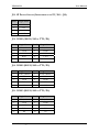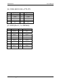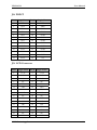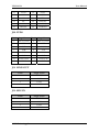
1
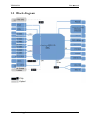
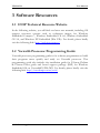
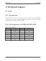
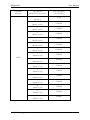
User Manual
VDX3-6754
with
DM&P Vortex86DX3
1GHz processor
Version 1.0
ICOP Technology Inc. VDX3-6754
User Manual
Copyright
The information in this manual is subject to change without notice for
continues improvement in the product. All rights are reserved. The
manufacturer assumes no reasonability for any inaccuracies that may be
contained in this document and makes no commitment to update or to keep
current the information contained in this manual.
No part of this manual may be reproduced, copied, translated or transmitted,
in whole or in part, in any form or by any means without the prior to written
permission of ICOP Technology Inc.
ⓒCopyright 2015 ICOP Technology Inc
Trademarks Acknowledgement
Vortex86DX3TM is the registered trademark of DM&P Electronics Inc.
Other brand names and product names that appear in this document are the
properties and registered trademarks of their respective owners. All names
mentioned herewith are served for identification purpose only.
ICOP Technology Inc.
I
VDX3-6754
User Manual
Revision History
Revision
1.0
Date
September, 2015
Remark
First version release
ICOP Technology Inc.
II
VDX3-6754
User Manual
Table of Contents
1 General Information ......................................................................................... 1 1.1 Overview .................................................................................................................................... 1 1.2 Block diagram ............................................................................................................................. 2 1.3 Specifications .............................................................................................................................. 3 1.4 Ordering Information ................................................................................................................. 5 1.4.1 VDX3-6754 ............................................................................................................................. 5 1.4.2 Cable Set .................................................................................................................................. 5 1.4.3 ICOP‐0096 .............................................................................................................................. 5 1.4.4 SATA DOM ............................................................................................................................ 6 2 Hardware Information ..................................................................................... 8 2.1 Dimension .................................................................................................................................. 8 2.2 Board Outline ............................................................................................................................. 9 2.3 Connector Location .................................................................................................................. 10 2.4 Connector and Jumper Summary .............................................................................................. 11 2.5 Pin Assignments & Jumper Settings .......................................................................................... 12 J1: JTAG ........................................................................................................................................ 12 J2: PS/2 Keyboard ......................................................................................................................... 12 J3: PS/2 Mouse .............................................................................................................................. 12 J4: SATA DOM ............................................................................................................................. 12 J5: SATA DOM Power .................................................................................................................. 13 J6: USB 0&1 ................................................................................................................................... 13 J7: LAN ......................................................................................................................................... 13 J8: VGA ......................................................................................................................................... 13 J9: Reset ......................................................................................................................................... 14 J10A: PC/104 Connector – 64 pin ................................................................................................. 14 ICOP Technology Inc.
III
VDX3-6754
User Manual
J10B: PC/104 Connector – 40 pin.................................................................................................. 15 J11: Buzzer ..................................................................................................................................... 15 J12: 4P Power Source (Interconnect to PC/104 – J10) ................................................................... 16 J13: COM1 (RS232/485 or TTL/P4) ............................................................................................. 16 J14: COM2 (RS232/485 or TTL/P5) ............................................................................................. 16 J15: COM3 (RS232/485 or TTL/P6) ............................................................................................. 16 J16: COM4 (RS232/485 or TTL/P7) ............................................................................................. 17 J17: GPIO (Port 0 / 1 or PWMx16) ............................................................................................... 17 J18: PRINT .................................................................................................................................... 18 J19: LCD Connector ...................................................................................................................... 18 J20: LVDS ...................................................................................................................................... 19 J21: LINE-OUT ............................................................................................................................ 19 J22: MIC-IN................................................................................................................................... 19 J23: Touchscreen Connector (Optional) ......................................................................................... 20 J24: Power Connector .................................................................................................................... 20 System Mapping ............................................................................................................................. 21 3 Software Resources ......................................................................................... 24 3.1 ICOP Technical Resource Website............................................................................................ 24 3.2 Vortex86 Processor Programming Guide .................................................................................. 24 4 Technical support ............................................................................................ 25 4.1 LCD ......................................................................................................................................... 25 4.1.1 Introduction ..................................................................................................................... 25 4.1.2 Pin Assignment of LVDS and TFT-LCD ......................................................................... 25 4.2 BIOS ........................................................................................................................................ 28 4.2.1 Introduction ..................................................................................................................... 28 4.2.2 CPU Clock Adjusting ....................................................................................................... 28 4.2.3 Console Redirection ......................................................................................................... 31 ICOP Technology Inc.
IV
VDX3-6754
User Manual
4.2.4 Serial ports Switching ....................................................................................................... 32 4.2.5 IDE Configuration ........................................................................................................... 33 4.2.6 Advanced PCI/PnP Setting .............................................................................................. 35 4.2.7 ACPI Enable .................................................................................................................... 36 4.2.8 LCD Panel setting ............................................................................................................ 37 Warranty ................................................................................................................... 39 ICOP Technology Inc.
V
VDX3-6754
User Manual
1 General Information
1.1 Overview
The VDX3-6754 PC/104 family of low-power x86 embedded controller is
designed to meet PC/104 specification with backward compatibility to
provide migration path for projects facing end-of-life challenges with their
existing x86 based PC/104 controller.
In addition, the VDX3-6754 family of controller is designed as a plug in
replacement, with backward compatibility to support legacy software to help
extend existing product life cycle without heavy re-engineering.
The VDX3-6754 is suitable for broad range of data-acquisition, industrial
automation, process control, automotive controller, AVL, intelligent vehicle
management device, medical device, human machine interface, robotics,
machinery control and more.
ICOP Technology Inc.
1
VDX3-6754
User Manual
1.2 Block diagraam
ICOP T
Technologyy Inc.
2
VDX3-6754
User Manual
1.3 Specifications
Processor
Cache
DM&P SoC CPU Vortex86DX3 1GHz
Real Time Clock with Lithium Battery Backup
L1:32K I-Cache, 32K D-Cache, L2 Cache:512KB
Bus
PC/104 Standard Compliant
System Memory
1GB/2GB DDR3 Onboard
Watchdog Timer
Software programmable from 30.5 us to 512 seconds x2
sets(Watchdog 1 fully compatible with M6117D)
VGA
Integrated 2D VGA chip with dual display support (VGA + TTL /
VGA + LVDS)
VGA: Maximum resolution up to 1920x1080 @ 60Hz
LVDS: Maximum resolution up to 1024x768 @ 60Hz
Single channel 24-bit LVDS
LAN
Integrated 10/100Mbps Ethernet x1
Audio
ALC262 (HD Audio)
Touch Controller PS/2 interface (Optional)
I/O Interface
SATA 7P Connector x1
RS-232/485 port x4
USB port (Ver. 2.0) x2
USB Hot SWAP x1(Optional)
Parallel port x1
16-bit GPIO port x1
10/100Mbps Ethernet port x1
ICOP Technology Inc.
3
VDX3-6754
User Manual
Connectors
SATA 7P for SATA x1
2.0mm 26-pin box header for Printer x1
20.mm 20-pin box header for 16-bit GPIO x1
2.0mm 10-pin box header for USB x1
2.0mm 10-pin box header for RS232 x4
2.0mm 44-pin box header for LCD x1
2.0mm 16-pin header for LVDS x1
2.0mm 8-pin header for Ethernet x1
2.0mm 10-pin box header for VGA x1
2.54mm 5-pin header for Keyboard x1
2.54mm 5-pin header for Mouse x1
2.54mm 4-pin header for -5V, -12V +12V, GND x1
2.54mm 2-pin header for Reset x1
1.25mm 6-pin wafer for JTAG x1
1.25mm 4-pin wafer for Line-out/MIC-in x2
1.25mm 4-pin wafer for Touch Screen x1
Power
Requirement
Single Voltage +5V @1.3A (Typical)
Weight
Dimensions
Operating
Temp.
80g
90mm x 96mm (3.54 x 3.77 inches)
-20oC ~ +70oC
-40oC ~ +85oC (Optional)
Free DOS, DOS 6.22, PCDOS 7.1, DR-DOS, x-DOS, OD/2, Windows 7,
Windows Embedded Standard 7, Windows Embedded Compact 7,
Operating
Windows Embedded Compact 6, Windows XP Professional, Windows
System Support
Embedded Standard(XPE), POS Ready(WePOS), Embedded Linux,
X-linux, QNX, Vxworks and FreeBSD.
ICOP Technology Inc.
4
VDX3-6754
User Manual
1.4 Ordering Information
1.4.1 VDX3-6754
Product Name
1GB DDR3 onboard
2GB DDR3 onboard
Touch function
VDX3-6754-1G
V
/
/
VDX3-6754-2G
/
V
/
VDX3-6754-1G-T
V
/
V
VDX3-6754-2G-T
/
V
V
1.4.2 Cable Set
Product Name
Cable-set-6754
Contents
NET4X2(2.0) x1
RS232(2.0) x4
USB(2.0) x1
PRINT(2.0) x1
VGA(2.0) x1
GPIO(2.0) x1
PS2KB(TEST) x2
CABLE-AUDIO-4P(1.25) x2
1.4.3ICOP‐0096
TFT to LVDS 18bits converter Product Name
ICOP-0096
Contents
ICOP-0096 x1
ICOP Technology Inc.
5
VDX3-6754
User Manual
1.4.4 SATA DOM
Product Name
MLC
SLC
0℃ ~ +70℃
-40℃ ~ +85℃
SDM-SST-2G-H-M
V
V
SDM-SST-4G-H-M
V
V
ISATA-8G-H-M
V
V
ISATA-16G-H-M
V
V
ISATA-32G-H-M
V
V
ISATA-4G-H-M-X
V
V
ISATA-8G-H-M-X
V
V
ISATA-16G-H-M-X
V
V
ISATA-32G-H-M-X
V
V
ISATA-1G-H-S
V
V
ISATA-2G-H-S
V
V
ISATA-4G-H-S
V
V
ISATA-8G-H-S
V
V
ISATA-16G-H-S
V
V
SDM-SST-2G-H-S-X
V
V
SDM-SST-4G-H-S-X
V
V
SDM-SST-8G-H-S-X
V
V
ISATA-16G-H-S-X
V
V
ICOP Technology Inc.
6
VDX3-6754
User Manual
Illustration of “SDM-SST” placed on VDX3-6754
(ISATA series illustration is the same)
The SATA DOM will be higher than the top of PC/104 connector 4
millimeter when the SATA DOM placed on VDX3-6754.
ICOP Technology Inc.
7
VDX3-6754
User Manual
2 Hardware Information
2.1 Dimension
ICOP Technology Inc.
8
VDX3-6754
User Manual
2.2 Board Outlin
ne
ICOP T
Technologyy Inc.
9
VDX3-6754
User Manual
2.3 Connector Location
ICOP Technology Inc.
10
VDX3-6754
User Manual
2.4 Connector and Jumper Summary
Nbr.
Name
Type of Connections
Pin Nbr
J1
JTAG
Wafer, 1.25mm, 1x6
6
J2
PS/2 Keyboard
Box Header, 2.54mm, 1x5
5
J3
PS/2 Mouse
Box Header, 2.54mm, 1x5
5
J4
SATA DOM
SATA 7P Connector, 7x1
7
J5
SATA DOM Power
Box Header, 2.0mm, 1x2
2
J6
USB
Pin Header, 2.54mm, 5x2
10
J7
LAN
Pin Header, 2.0mm, 4x2
8
J8
VGA
Pin Header, 2.0mm, 5x2
10
J9
Reset
Pin Header, 2.54mm, 1x2
2
J10A
PC/104 Connector – 64 pin
Box Header, 2.54mm, 32x2
64
J10B
PC/104 Connector – 40 pin
Box Header, 2.54mm, 20x2
40
J11
Buzzer
Pin Header, 2.54mm, 1x2
2
J12
4P Power Source (Interconnect to
PC/104 – J10)
Pin Header, 2.54mm, 4x1
4
J13
COM1(RS232/485 or TTL/P4)
Box Header, 2.0mm, 5x2
10
J14
COM2(RS232/485 or TTL/P5)
Box Header, 2.0mm, 5x2
10
J15
COM3(RS232/485 or TTL/P6)
Box Header, 2.0mm, 5x2
10
J16
COM4(RS232/485 or TTL/P7)
Box Header, 2.0mm, 5x2
10
J17
GPIO (Port 0 / 1 or PWMx16)
Box Header, 2.0mm, 10x2
20
J18
PRINT
Box Header, 2.0mm, 13x2
26
J19
LCD Connector
Box Header, 2.0mm, 22x2
44
J20
LVDS
Pin Header, 2.0mm, 8x2
16
J21
LINE-OUT
Wafer, 1.25mm , 4x1
4
J22
MIC-IN
Wafer, 1.25mm , 4x1
4
J23
Touchscreen Connector
(Optional)
Wafer, 1.25mm , 4x1
4
J24
Power Connector
Terminal Block 5.0mm, 2x1
2
PWR
LED
Power Active LED (Red)
SMD LED
LED 3
LAN LINK/Active LED (Green)
SMD LED
LED 4
LAN Duplex LDE (Yellow)
SMD LED
ICOP Technology Inc.
11
VDX3-6754
User Manual
2.5 Pin Assignments & Jumper Settings
J1: JTAG
Pin# Single Name Pin # Single Name
1.
VCC
2
GND
3
TCK
4
TDO
5
TDI
6
TMS
J2: PS/2 Keyboard
Pin# Single Name Pin # Single Name
1.
KBCLK
2
KBDATA
3
NC
4
GND
5
VCC
J3: PS/2 Mouse
Pin# Single Name Pin # Single Name
1.
MSCLK
2
MSDATA
3
NC
4
GND
5
VCC
J4: SATA DOM
Pin# Single Name Pin # Single Name
1.
GND
2
TX+
3
TX-
4
GND
5
RX-
6
RX+
7
GND
*The pin 7 supports +5V (Optional)
ICOP Technology Inc.
12
VDX3-6754
User Manual
J5: SATA DOM Power
Pin# Single Name Pin # Single Name
1.
VCC
2
GND
J6: USB 0&1
Pin# Single Name Pin # Single Name
1.
VCC
2
VCC
3
LUSBD0-
4
LUSBD1-
5
LUSBD0+
6
LUSBD1+
7
GND
8
GND
9
GGND
10
GGND
*USB1 supports USB hot SWAP (Optional)
J7: LAN
Pin# Single Name Pin #
Single Name
1.
LTX+
2
LTX-
3
LRX+
4
DUPLEX
5
LED0+
6
LRX-
7
LED1+
8
LINK/ACTIVE
J8: VGA
Pin# Single Name Pin # Single Name
1.
R OUT
2
GND
3
G OUT
4
GND
5
B OUT
6
GND
7
HSYNC_A
8
GND
9
VSYNC_A
10
GND
ICOP Technology Inc.
13
VDX3-6754
User Manual
J9: Reset
Pin# Single Name Pin # Single Name
1.
RST_SW
2
GND
J10A: PC/104 Connector – 64 pin
Pin# Single Name Pin # Single Name
1.
IOCHCHK*
2
GND
3
SD7
4
RESETDRV
5
SD6
6
VCC
7
SD5
8
IRQ9
9
SD4
10
-5V
11
SD3
12
RDQ2
13
SD2
14
-12V
15
SD1
16
OWS
17
SD0
18
+12V
19
IOCHRDY
20
GND
21
AEN
22
SMEMW*
23
SA19
24
SMEMR*
25
SA18
26
IOW*
27
SA17
28
IOR*
29
SA16
30
DACK3*
31
SA15
32
DRQ3
33
SA14
34
DACK1*
35
SA13
36
DRQ1*
37
SA12
38
REFRESH*
39
SA11
40
SYSCLK
41
SA10
42
IRQ7
43
SA9
44
IRQ6
45
SA8
46
IRQ5
47
SA7
48
IRQ4
49
SA6
50
IRQ3
51
SA5
52
DACK2*
53
SA4
54
TC
55
SA3
56
BALE
ICOP Technology Inc.
14
VDX3-6754
User Manual
57
SA2
58
VCC
59
SA1
60
OSC
61
SA0
62
GND
63
GND
64
GND
J10B: PC/104 Connector – 40 pin
Pin# Single Name Pin # Single Name
1.
GND
2
GND
3
MEMCS16*
4
SBHE*
5
IOCS16*
6
SA23
7
IRQ10
8
SA22
9
IRQ11
10
SA21
11
IRQ12
12
SA20
13
IRQ15
14
SA19
15
IRQ14
16
SA18
17
DACK0*
18
SA17
19
DRQ0
20
MEMR*
21
DACK5*
22
MEMW*
23
DRQ5
24
SD8
25
DACK6*
26
SD9
27
DRQ6
28
SD10
29
DACK7
30
SD11
31
DRQ7
32
SD12
33
VCC
34
SD13
35
MASTER*
36
SD14
37
GND
38
SD15
39
GND
40
NC
J11: Buzzer
Pin# Single Name Pin # Single Name
1.
Buzzer
2
VCC
ICOP Technology Inc.
15
VDX3-6754
User Manual
J12: 4P Power Source (Interconnect to PC/104 – J10)
Pin# Single Name
1.
-5V
2
-12V
3
+12V
4
GND
J13: COM1 (RS232/485 or TTL/P4)
Pin#
Single Name
Pin #
Single Name
1.
DCD1/1RS485-
2
RXD1/1RS485+
3
TXD1
4
DTR1
5
GND
6
DSR1
7
RTS1
8
CTS1
9
RI1
10
NC
J14: COM2 (RS232/485 or TTL/P5)
Pin#
Single Name
Pin #
Single Name
1.
DCD1/1RS485-
2
RXD1/1RS485+
3
TXD1
4
DTR1
5
GND
6
DSR1
7
RTS1
8
CTS1
9
RI1
10
NC
J15: COM3 (RS232/485 or TTL/P6)
Pin#
Single Name
Pin #
Single Name
1.
DCD1/1RS485-
2
RXD1/1RS485+
3
TXD1
4
DTR1
5
GND
6
DSR1
7
RTS1
8
CTS1
9
RI1
10
NC
ICOP Technology Inc.
16
VDX3-6754
User Manual
J16: COM4 (RS232/485 or TTL/P7)
Pin#
Single Name
Pin #
Single Name
1.
DCD1/1RS485-
2
RXD1/1RS485+
3
TXD1
4
DTR1
5
GND
6
DSR1
7
RTS1
8
CTS1
9
RI1
10
NC
J17: GPIO (Port 0 / 1 or PWMx16)
Pin# Single Name Pin #
Single Name
1.
GND
2
VCC
3
GP00
4
GP10
5
GP01
6
GP11
7
GP02
8
GP12
9
GP03
10
GP13
11
GP04
12
GP14
13
GP05
14
GP15
15
GP06
16
GP16
17
GP07
18
GP17
19
VCC
20
GND
ICOP Technology Inc.
17
VDX3-6754
User Manual
J18: PRINT
Pin# Single Name Pin #
Single Name
1.
STB-
14
AFD-
2
PD0
15
ERR-
3
PD1
16
INIT-
4
PD2
17
SLIN-
5
PD3
18
GND
6
PD4
19
GND
7
PD5
20
GND
8
PD6
21
GND
9
PD7
22
GND
10
ACK-
23
GND
11
BUSY
24
GND
12
PE
25
GND
13
SLCT
26
NC
J19: LCD Connector
Pin# Single Name Pin # Single Name
1.
+3.3V
2
+3.3V
3
LG2
4
LG3
5
LG4
6
LG5
7
NC
8
NC
9
LR0
10
LR1
11
LR2
12
LR3
13
LR4
14
LR5
15
GND
16
NC
17
NC
18
NC
19
NC
20
GND
21
NC
22
NC
23
LB0
24
LB1
25
LB2
26
LB3
27
LB4
28
LB5
29
NC
30
NC
31
LG0
32
LG1
ICOP Technology Inc.
18
VDX3-6754
User Manual
33
GND
34
GND
35
NC
36
LCLK
37
NC
38
LDE
39
NC
40
LHSYNC
41
NC
42
LVSYNC
43
LBACKL
44
LVDDEN
J20: LVDS
Pin#
Single Name
Pin #
Single Name
1.
VCC3 (+3.3V)
2
VCC3 (+3.3V)
3
GND
4
GND
5
Y0P
6
Y0M
7
Y1M
8
Y1P
9
Y2P
10
Y2M
11
GND
12
GND
13
CLKOUTM
14
CLKOUTP
15
Y3M
16
Y3P
J21: LINE-OUT
Pin#
Single Name
1
LOUTR
2
GND
3
GND
4
LOUTL
J22: MIC-IN
Pin#
Single Name
1
MICVREF
2
GND
3
GND
4
MIC-IN
ICOP Technology Inc.
19
VDX3-6754
User Manual
J23: Touchscreen Connector (Optional)
Pin#
Single Name
1
Y-
2
X-
3
Y+
4
X+
No PS/2 Mouse when Touch Screen is selected.
J24: Power Connector
Pin#
Single Name
1
+5V
2
GND
ICOP Technology Inc.
20
VDX3-6754
User Manual
System Mapping
Memory Mapping
Address
Description
Usage
00000000 – 0009FFFF
System RAM
*
000A0000 – 000AFFFF
EGA/VGA Video Memory
*
000B0000 – 000B7FFF
MDA RAM, Hercules graphics display RAM
*
000B8000 – 000BFFFF
CGA display RAM
*
000C0000 – 000C7FFF
EGA/VGA BIOS ROM
*
000C8000 – 000CFFFF
Boot ROM enable
000CC000 – 000CFFFF
Console Redirection enable
000D0000 – 000D7FFF
Expansion ROM space
000D8000 – 000D8FFF
SPI Flash Emulation Floppy A Enable
000DC000 – 000DFFFF
Expansion ROM Space
000E0000 – 000EFFFF
USB Legacy SCSI ROM space
000F0000 – 000FFFFF
Motherboard BBIOS
*
Standard OpenHCD USB Host Controller
*
FEFBB400 – FEFBB4FF
Onboard Ethernet Adapter
*
FEFDB800 – FEFDBFFF
Standard Enhanced PCI to USB Host Controller
*
FEFDBC00 – FEFDBCFF
ICOP Technology Inc.
21
VDX3-6754
User Manual
I/O Mapping
Address
Description
Usage
0000h – 000Fh
DMA 8237-1
*
0020h – 0021h
PIC 8259-1
*
0022h – 0023h
Indirect Access Registers (6117D configuration port)
*
0040h –0043h
Timer Counter 8254
*
0060h
Keyboard / Mouse data port
0061h
Port B + NMI control port
0062h – 0063h
*
8051 download 4k address counter
0064h
Keyboard/ Mouse status/ command port
0065h
WatchDog0 reload counter
0070h – 0071h
CMOS RAM port
*
0072h – 0075h
MTBF control register
*
0078h – 007Ch
GPIO port 0,1,2,3,4 default setup
*
0080h – 008Fh
DMA page register
0092h
System control register
*
0093h – 0097h
GPIO port 6,7,8,9,A direction control
*
0098h – 009Dh
GPIO port 0,1,2,3,4,5 direction control
*
00A0h – 00A1h
PIC 8259-2
*
00A8h – 00ADh
WatchDog1 control counter
*
00AEh
WatchDog1 reload counter
*
00C0h – 00DFh
DMA 8237-2
*
00E0h – 00EFh
DOS 4G Page access
*
0100h – 0105h
GPIO port 5,6,7,8,9,A default setup
*
0170h – 0177h
IDE 1(IRQ 15)
*
0278h – 027Fh
Printer port (IRQ7, DMA 0)
*
02E8h – 02EFh
COM4 (IRQ 11)
*
02F8h – 02EFh
COM2 (IRQ 3)
*
03E8h – 03EFh
COM3 (IRQ 10)
*
IDE1 ATAPI device control write only register
*
03F8h – 03FFh
COM1 (IRQ 4)
*
0480h – 048Fh
DMA High page register
*
0490h – 0499h
Instruction counter register
*
04D0h – 04D1h
8259 Edge / level control register
*
0CF8h – 0CFFh
PCI configuration port
*
DE00h – DEFFh
On board LAN
*
SPI Flash BIOS control register
*
03F6h
FC00h – FC05h
ICOP Technology Inc.
22
VDX3-6754
FC08h – FC0Dh
User Manual
External SPI BUS control register
*
IRQ Mapping
Address
Description
Usage
IRQ0
System Timer
*
IRQ1
Keyboard Controller
*
IRQ2
Cascade for IRQ8~15
IRQ3
Serial port 2
*
IRQ4
Serial port 1
*
IRQ5
USB
*
IRQ6
USB
IRQ7
Printer Port
*
IRQ8
Real Timer Clock
*
IRQ9
USB/ Ethernet 10/ 100M LAN
*
IRQ10
Serial Port 3
*
IRQ11
Serial Port 4
*
IRQ12
Mouse
*
IRQ13
Math Coprocessor
*
IRQ14
Multimedia Device
*
IRQ15
Hard Disk Controller #2
*
DMA Mapping
Address
Description
Usage
DMA0
DMA1
DMA2
DMA3
DMA4
DMA5
DMA6
DMA7
ICOP Technology Inc.
23
VDX3-6754
User Manual
3 Software Resources
3.1 ICOP Technical Resource Website
In the following website, you will find our latest user manuals, including OS
support resources systems such as evaluation images for Windows
Embedded Compact 7, Windows Embedded CE 6.0, Windows Embedded
CE 5.0, and Windows XP Embedded (Win XPe). For details, please kindly
visit the following link: http://tech.icop.com.tw/
3.2 Vortex86 Processor Programming Guide
Vortex86 processor programming guide is for software programmers to build
their programs more quickly and easily on Vortex86 processor. This
programming guide also includes the installation guide for X-Linux, Debian
& Ubuntu Linux guide and board support package (BSP) for Windows
Embedded OS on Vortex86SX/DX/MX. For details, please kindly visit the
following link: http://www.dmp.com.tw/tech/
ICOP Technology Inc.
24
VDX3-6754
User Manual
4 Technical support
4.1 LCD
4.1.1 Introduction
The VDX3-6754 offers two different interfaces which support maximum
resolution up to 1920 x 1080 (at 60MHz) connecting to LCD Flat Panel:
18-bit/24-bit TFT-LCD and 24-bit LVDS.
4.1.2 Pin Assignment of LVDS and TFT-LCD
LVDS Pin Assignment
LVDS Pin#
Pin Name
LVDS Pin#
Pin Name
1
VCC3 (+3.3V)
2
VCC3 (+3.3V)
3
GND
4
GND
5
Y0P
6
Y0M
7
Y1M
8
Y1P
9
Y2P
10
Y2M
11
GND
12
GND
13
CLKOUTM
14
CLKOUTP
15
Y3M
16
Y3P
ICOP Technology Inc.
25
VDX3-6754
User Manual
TFT Flat Panel Data Output
LCD Pin# Vortex86DX3 Pin Name
DIGITAL 18 bits
RGB 24 bits
1
LCDVCC (+3.3V)
VDD
VDD
2
LCDVCC (+3.3V)
VDD
VDD
3
FPD12
G2
G4
4
FPD13
G3
G5
5
FPD14
G4
G6
6
FPD15
G5
G7
7
FPD16
/
R0
8
FPD17
/
R1
9
FPD18
R0
R2
10
FPD19
R1
R3
11
FPD20
R2
R4
12
FPD21
R3
R5
13
FPD22
R4
R6
14
FPD23
R5
R7
15
GND
VSS
VSS
16
NC
/
/
17
NC
/
/
18
NC
/
/
19
NC
/
/
20
GND
VSS
VSS
21
PPD0
/
B0
22
PPD1
/
B1
23
PPD2
B0
B2
24
PPD3
B1
B3
25
PPD4
B2
B4
26
PPD5
B3
B5
27
PPD6
B4
B6
28
PPD7
B5
B7
29
PPD8
/
G0
30
PPD9
/
G1
31
PPD10
G0
G2
32
PPD11
G1
G3
33
GND
VSS
VSS
34
GND
VSS
VSS
35
NC
/
/
ICOP Technology Inc.
26
VDX3-6754
User Manual
36
FP1CLK
XCLK
XCLK
37
NC
/
/
38
FP1DE
DEN
DEN
39
NC
/
/
40
FP1HS
HSYNC
HSYNC
41
NC
/
/
42
FP1VS
VSYNC
VSYNC
43
FPENBLT
ADJ
ADJ
44
FPENVDD
VDDEN
VDDEN
ICOP Technology Inc.
27
VDX3-6754
User Manual
4.2 BIOS
4.2.1 Introduction
Featuring AMI BIOS, the VDX3-6754 is the one stable PC/104 computer
board for your application. In this section, we will introduce you some basic
AMI BIOS settings such as CPU speed adjusting, console redirection, and,
IDE Configuration etc.
4.2.2 CPU Clock Adjusting
Adjusting CPU clock frequency is available on VDX3-6754. In the BIOS
setup manual, you will find different options from 1 to F (please refer to the
table in next page) for CPU clock frequency.
For example, when you choose [1], the CPU clock frequency will be
1000MHz*(15/16) = 937MHz.
ICOP Technology Inc.
28
VDX3-6754
CPU Main
Frequency
1GHz
User Manual
CPU Divisor
MSR CFCFCF00 32:39
CPU Frequency
after dividing
0
(Divide 1)
1GHz
1
(Divide 15/16)
937MHz
2
(Divide 14/16)
875MHz
3
(Divide 13/16)
812MHz
4
(Divide 12/16)
750MHz
5
(Divide 11/16)
687MHz
6
(Divide 10/16)
625MHz
7
(Divide 9/16)
562MHz
8
(Divide 8/16)
500MHz
9
(Divide 7/16)
437MHz
A
(Divide 6/16)
375MHz
B
(Divide 5/16)
312MHz
C
(Divide 4/16)
250MHz
D
(Divide 3/16)
187MHz
E
(Divide 2/16)
125MHz
F
(Divide 1/16)
62MHz
ICOP Technology Inc.
29
VDX3-6754
User Manual
Path: Advanced >NorthBridge Configuration >CPU Configuration
>MSR CFCFCF00 32:39 >CPU Speed Divide By [
]
ICOP Technology Inc.
30
VDX3-6754
User Manual
4.2.3 Console Redirection
Access to computer board through serial port, you can work on VDX3-6754
without VGA display or monitor. The default access port is COM1 and
disabled. If you would like to use this function, please go to the path below
to enable Console Redirection.
Path: Advanced >Remote Access Configuration >Remote Access
[Enabled]
ICOP Technology Inc.
31
VDX3-6754
User Manual
4.2.4 Serial ports Switching
Serial ports on VDX3-6754 are set RS232 as default. If you need RS485 be
your default serial ports. Please contact your contact window directly or mail
[email protected].
And you can refer to the below instruction to select the IRQ mode according
to your demands.
Path: Advanced >Serial/Parallel Port Configuration
ICOP Technology Inc.
32
VDX3-6754
User Manual
4.2.5 IDE Configuration
The default IDE configuration is for Windows Operating System, and the
setting as below:
Onboard IDE Operate Mode: [Legacy Mode]
IDE Compatibility: [Disabled].
If you would like to use Linux on VDX3-6754, please follow below
instructions:
Onboard IDE Operate Mode: [Native Mode]
IDE Compatibility: [Enabled].
Path of Onboard IDE Operate Mode:
Advanced >IDE Configuration >Onboard IDE Operate Mode
[Native Mode]
ICOP Technology Inc.
33
VDX3-6754
User Manual
Path of IDE Compatibility:
Advanced > SouthBridge Configuration > MISC Configuration >
IDE Compatibility [Enabled]
ICOP Technology Inc.
34
VDX3-6754
User Manual
4.2.6 Advanced PCI/PnP Setting
Two statuses for IRQ setting:
[Reserved]: IRQ will be free to be allocated by ISA device, not PCI device.
[Available]: IRQ will be allocated by both ISA device and PCI device.
Path: PCIPnP >IRQ
ICOP Technology Inc.
35
VDX3-6754
User Manual
4.2.7 ACPI Enable
To install Windows 7 on ICOP computer boards, please enable ACPI as the
following instruction.
Path: Advanced >Power Management Configuration >
ACPI Configuration >ACPI Aware O/S
ICOP Technology Inc.
36
VDX3-6754
User Manual
4.2.8 LCD Panel setting
The default setting of Boot Display
[VBIOS] are for VGA signal.
Device [CRT] and the LCD Panel Index
If you need to use LCD panel with VDX3-6754, please follow below instructions:
Boot Display Device [IPD]
LCD Panel Index according to your LCD resolution from 1 to 5.
Options
Resolution of the LCD Panel
0
640 x 480
1
800 x 480
2
800 x 600
3
1024 x 600
4
1024 x 768
Path of Boot Display Device setting:
Boot >Boot Settings Configuration >Boot Display Device [IPD]
ICOP Technology Inc.
37
VDX3-6754
Path of LCD Panel Index setting:
Boot >Boot Settings Configuration >LCD Panel Index [
User Manual
]
ICOP Technology Inc.
38
VDX3-6754
User Manual
Warranty
This product is warranted to be in good working order for a period of one
year (12 months) from the date of purchase. Should this product fail to be in
good working order at any time during this period, we will, at our option,
replace or repair it without additional charge except as set forth in the
following terms. This warranty does not apply to products damaged by
misuse, modifications, accident or disaster. Vendor assumes no liability for
any damages, lost profits, lost savings or any other incidental or consequential
damage resulting from the use, misuse of, originality to use this product.
Vendor will not be liable for any claim made by any other related party.
Return authorization must be obtained from the vendor before returned
merchandise is accepted. Authorization can be obtained by calling or faxing
the vendor and requesting a Return Merchandise Authorization (RMA)
number. Returned goods should always be accompanied by a clear problem
description. Should you have questions about warranty and RMA service,
please contact us directly.
ICOP Technology Inc.
Address: No. 15 Wugong 5th Road, Xinzhuang Dist.
New Taipei City, Taiwan (R.O.C.) 24890
TEL: +886-2-8990-1933
FAX: +886-2-8990-2045
Mail: [email protected]
Website: http://www.icop.com.tw
ICOP Technology Inc.
39