1
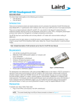
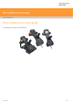
Laird Wireless Development Kit Application Note v1.0 Part # BISDK02BI-02 Applicable to the following Bluetooth module part numbers:TRBLU23-00200-0x, TRBLU23-00300-0x, BTM402-0x, BTM404-0x OVERVIEW Laird’s Wireless Development Kit provides a platform for rapid prototyping of wireless connectivity, providing options for the development of Bluetooth applications. This manual is for Rev. 03 of the development PCB. For Rev. 02 of the PCB, please refer to Version 1.0 of this application note. 1. INTRODUCTION The Laird Wireless Development Kit is designed to support the rapid development of applications and software for the Laird range of Bluetooth modules. It is applicable not only to the default module (TRBLU23-00200-0x), but also to TRBLU2300300-0x, BTM402-0x, and BTM404-0x. More information regarding these products is available from the Laird website. Package Contents All kits contain the following items: Development Board The motherboard is used to mount your chosen wireless module, providing the RS-232 interface and access to all the module interface pins. USB cable The USB cable can be used as one of the options to provide power for the Dev Kit via the onboard connector. Serial cable RS-232 interface cable to provide the communication between your host pc and your choice of wireless module. The serial cable can also be used as an option to power the motherboard and module from pin 9. Bluetooth USB adapter Development Kit includes a FREE USB Bluetooth adaptor, Laird part # BRBLU03-010A0. This robust, Class 1 Bluetooth Adapter has native support for Microsoft Bluetooth software stacks since Windows XP SP2. Three Mounting Spacers Mounting spacers for securing your Bluetooth module to the motherboard. EZURiO Terminal application PC-based terminal emulation software, specifically designed to help the development and diagnostics of applications on the Laird range of modules. Documentation Development Kit user guide, board design circuit diagrams, and quick start guide. Embedded Wireless Solutions Support Center: http://ews-support.lairdtech.com www.lairdtech.com/bluetooth Laird Technologies Americas: +1-800-492-2320 Europe: +44-1628-858-940 Hong Kong: +852-2268-6567 x026 Wireless Development Kit Application Note 2. Wireless Module Development Board The development board allows the Laird Bluetooth Module to be connected to a PC. The development board provides RS232 level conversion through a standard 9-way D type connector to all pins of the 40-way Hirose connectors used by the Bluetooth modules. A separate connector is provided for PCM audio use with the 40 way Laird Bluetooth modules. This 10 way PCM connector is provided for use with external codec boards (not supplied); reference design application notes are available from Laird but Laird does not guarantee the availability of any component mentioned within. 3. GETTING TO KNOW THE DEVELOPMENT BOARD Reset Switch 40-way connector PCM Output 9-way DEE PSU Options: USB 2.1mm Jack Screws or RS232 Pin 9 50-way connector (Not required for Bluetooth) modules) RS-232 Level Shifter Figure 1: Development Board 4. POWER SUPPLY Input Voltage Minimum Typical Maximum 3.6V 5V 6V The development board provides a number of options to provide power to the module: 5V Power from a USB port Power from an external power supply via screw terminals Power from an external mains power block via a 2.1 mm DC connector Power via Pin 9 of the RS232 adaptor The developer kit includes a USB cable to provide power to the development board. This should be plugged into a PC USB port, a USB hub, or a mains adaptor with a USB output. If a hub is used, it should be a powered USB hub to ensure that sufficient current is available at the port being used. The Bluetooth Intelligent Serial Module (BISMII) and BISM II PA modules can be driven by the current available at a USB port. Embedded Wireless Solutions Support Center: http://ews-support.lairdtech.com www.lairdtech.com/bluetooth Laird Technologies Americas: +1-800-492-2320 Europe: +44-1628-858-940 Hong Kong: +852-2268-6567 x026 Wireless Development Kit Application Note Jumper JP2 is used to select an external power source on the screw terminals. Figure 2: JP2 Settings SW1 (slide switch) provides the power on/off for the module but does not isolate the power from other components of the development board. S1 (push button TACT switch) provides a reset signal to both the 40- and 50-way connectors. Note that the reset polarity is different for the 40- and 50-way pinouts. This is accomplished by circuitry on the development board, providing an active HIGH reset for the 40-way connector and an active LOW for the 50-way connector. Users connecting a reset signal to the test points on the board should be aware that there is a 10kΩ pulldown on the 40-way reset pin and an open collector transistor connected to the 50-way reset pin. Refer to the schematics available on the CD. Note: The 50-way connector is not used for Bluetooth modules. An alternative method of powering the development kit is to supply power to Pin 9 of the RS-232 connector. If this method is used, no other power supplies should be connected to the board. Pins 2 and 3 of Jumper 8 on the development board need to be connected to allow power to be derived from pin 9 of the serial port. In this mode the ring indicator is not available from the RS-232 interface. Note that J8 is fitted with a wire link in the default position. This must be removed and replaced with a jumper or wire link to enable Pin 9 power. Pin 9 Power Standard Setting Figure 3: J8 Settings Embedded Wireless Solutions Support Center: http://ews-support.lairdtech.com www.lairdtech.com/bluetooth Laird Technologies Americas: +1-800-492-2320 Europe: +44-1628-858-940 Hong Kong: +852-2268-6567 x026 Wireless Development Kit Application Note 5. RS-232 SERIAL INTERFACE This provides a direct interface to any standard RS-232 port on a PC or peripheral. The 9-way D type connector can be plugged straight into a serial port on a PC or peripheral. If access to the serial port is restricted, the serial cable provided can be used to connect the development board to the PC. The development board contains a level shifter on the RX, TX, CTS, RTS, DTR, DSR, RI, and DCD signals that converts between the 3.3 V levels required on the module to the standard RS-232 levels. The level shifter can have its outputs permanently enabled or enabled only when the module is active (i.e., not in sleep mode). The latter is useful when a defined state is required at the RS-232 interface as the module enters and exits its low power modes. The behaviour is determined by the setting of J10 which is located behind the USB socket at the rear of the board. The normal setting is Always Enabled. Figure 4: J10 Settings If digital signal levels are required at the RS-232 connector, these can be achieved by removing the level shifter and populating the PCB pads that are then exposed with zero ohm links. 6. SOFTWARE The development board connects any Hirose connector based Laird Bluetooth Module to the serial port of a PC or other device. From a PC you can communicate with the module using any Terminal Emulator software such as HyperTerminal, Procomm, or the EZURiO Terminal application supplied. EZURiO Terminal is a terminal emulation application capable of running on Windows 98, Me, 2000, XP, and Windows 7operating systems. It was developed specifically to aid development and testing of Laird modules. It allows connection to serial devices using any combination of the communications parameters listed in Table 2. Table 1: Communication Parameters COM Port: 1 to 255 Baud rate: 300 to 921600 Parity: None, Odd, Even Data Bits: 7 or 8 Stop Bits: 1 or 2 Handshaking: None or CTS/RTS The benefits of using EZURiO Terminal are: Status of DSR, CTS, DCD, and RI are continuously displayed DTR on the host PC can be directly controlled via a check box Embedded Wireless Solutions Support Center: http://ews-support.lairdtech.com www.lairdtech.com/bluetooth Laird Technologies Americas: +1-800-492-2320 Europe: +44-1628-858-940 Hong Kong: +852-2268-6567 x026 Wireless Development Kit Application Note RTS can be directly controlled BREAK signals can be sent Scripts can be run to assist Additional built-in features speed development Laird includes a “Data Transfer Test” mode allowing data to be sent as fast as the handshaking permits. This feature is useful for testing the bit transfer rate of a Bluetooth connection. The EZURiO Terminal application is provided on the CD included with this kit; updates are also available from our website: http://www.lairdtech.com/Products/Wireless-M2M-and-Telematics-Solutions/Bluetooth-Module/ 7. INTERFACE SPECIFICATION 7.1 Serial port connector The pin-out for the 9-way D type connector is shown in Table 3. Note: The direction is as seen from the module’s perspective. Table 2: Pin Definitions Pin Description Signal Direction 1 Data Carrier Detect DCD Output 2 Transmit Data TD Output 3 Receive Data RD Input 4 Data Set Ready DSR Input 5 Ground GND --- 6 Data Terminal Ready DTR Output 7 Clear To Send CTS Input 8 Request To Send RTS Output 9 Board Power or Ring Indicator RI or Power Output 7.2 Module Breakout Connectors All of the pins from the 40- and 50-way connectors, with the exception of VCC, are available on each of two rows of plated through holes on the long sides of the board. These translate directly to the pin layout of the module receptacles, allowing access to all of the module pins. Pin 1 is indicated by an indent on the silk screen. The format of the holes allows the fitting of your choice of connectors, or they can be used for directly soldering test wires to the board. Both are laid out on a standard 2.54 mm (0.1 inch) pitch. 7.3 PCM Interface The Development board provides a dedicated audio interface for the Bluetooth modules. The pins provide the developer with access to the module’s PCM lines as well as providing power to allow additional audio hardware to be developed. Embedded Wireless Solutions Support Center: http://ews-support.lairdtech.com www.lairdtech.com/bluetooth Laird Technologies Americas: +1-800-492-2320 Europe: +44-1628-858-940 Hong Kong: +852-2268-6567 x026 Wireless Development Kit Application Note Laird has developed a range of audio codec application notes that can be used to develop boards that can be plugged directly onto this interface to support audio application development. More details of the PCM interface are available in the Audio Codec Board Applications Notes. J11 can be used to provide loopback capability when testing external audio codec. When the jumper is moved, it loops back the signal from PCM_OUT to PCM_IN. The default position disables loopback. Loopback Enabled Default Figure 5: J11 Settings 7.4 Board Configuration Jumpers Table 3: Jumpers Jumper Description JP1 Breaks the supply to the module for current measurements JP2 Selects external power supply for Siemens modules JP8 Selects pin 9 power (fitted as wire link) J10 Selects low power mode for RS-232 level shifter J11 PCM Loopback (not available on Rev 02 boards) Embedded Wireless Solutions Support Center: http://ews-support.lairdtech.com www.lairdtech.com/bluetooth Laird Technologies Americas: +1-800-492-2320 Europe: +44-1628-858-940 Hong Kong: +852-2268-6567 x026 Wireless Development Kit Application Note 8. OTHER FEATURES 8.1 Power Consumption Measurement A removable jumper JP1 is provided to break the supply line directly to the modules, allowing the current consumption to be measured. For normal operation JP1 must be fitted. Note: This only measures the current consumption of the module, and not of the level shifter or other peripheral circuitry. 8.2 USB Access USB access can be provided to allow a direct USB connection to a Bluetooth HCI module. To do this fit resistor pads R17 and R18 on the development kit with zero Ohm links. Note that if this is done and the unit is then connected to a USB host port, it will be powered from that same port. Do not attempt to use any other power source for the development kit when operating in this mode. This is not relevant for modules with a UART interface. 9. ADDITIONAL DOCUMENTATION For use with audio applications, application notes are available to describe optional audio codec boards that can be designed to connect to connector J5. These are: ACC-005 Winbond W61360 Audio Codec Board Manual ACC-006 OKI 7702 Audio Codec Board Manual ACC-007 OKI 7705 Multi-channel Audio Codec Board Manual The schematic of the board is available (B47DR-SC1C-03.pdf). Please request from your local FAE. REVISION HISTORY Revision Date 1.0 18 Apr 2013 Description Initial Release Embedded Wireless Solutions Support Center: http://ews-support.lairdtech.com www.lairdtech.com/bluetooth Initiated By Jonathan Kaye Laird Technologies Americas: +1-800-492-2320 Europe: +44-1628-858-940 Hong Kong: +852-2268-6567 x026