1
USER′S MANUAL
S3F401F
16/32-BIT RISC
MICROPROCESSOR
November, 2007
REV 1.00
Confidential Proprietary of Samsung Electronics Co., Ltd
Copyright © 2007 Samsung Electronics, Inc. All Rights Reserved
Important Notice
The information in this publication has been carefully
checked and is believed to be entirely accurate at
the time of publication. Samsung assumes no
responsibility, however, for possible errors or
omissions, or for any consequences resulting from
the use of the information contained herein.
Samsung reserves the right to make changes in its
products or product specifications with the intent to
improve function or design at any time and without
notice and is not required to update this
documentation to reflect such changes.
This publication does not convey to a purchaser of
semiconductor devices described herein any license
under the patent rights of Samsung or others.
Samsung makes no warranty, representation, or
guarantee regarding the suitability of its products for
any particular purpose, nor does Samsung assume
any liability arising out of the application or use of
any product or circuit and specifically disclaims any
and all liability, including without limitation any
consequential or incidental damages.
"Typical" parameters can and do vary in different
applications. All operating parameters, including
"Typicals" must be validated for each customer
application by the customer's technical experts.
Samsung products are not designed, intended, or
authorized for use as components in systems
intended for surgical implant into the body, for other
applications intended to support or sustain life, or for
any other application in which the failure of the
Samsung product could create a situation where
personal injury or death may occur.
Should the Buyer purchase or use a Samsung
product for any such unintended or unauthorized
application, the Buyer shall indemnify and hold
Samsung and its officers, employees, subsidiaries,
affiliates, and distributors harmless against all
claims, costs, damages, expenses, and reasonable
attorney fees arising out of, either directly or
indirectly, any claim of personal injury or death that
may be associated with such unintended or
unauthorized use, even if such claim alleges that
Samsung was negligent regarding the design or
manufacture of said product.
S3F401F 16/32-Bit RISC Microprocessor
User's Manual, Revision 1.00
Publication Number: 21-S3-F401F-112007
Copyright © 2007 Samsung Electronics Co., Ltd.
All rights reserved. No part of this publication may be reproduced, stored in a retrieval system, or transmitted in
any form or by any means, electric or mechanical, by photocopying, recording, or otherwise, without the prior
written consent of Samsung Electronics.
Samsung Electronics' microcontroller business has been awarded full ISO-14001
certification (BSI Certificate No. FM24653). All semiconductor products are designed
and manufactured in accordance with the highest quality standards and objectives.
Samsung Electronics Co., Ltd.
San #24 Nongseo-Dong, Giheung-Gu
Yongin-City, Gyunggi-Do, Korea
C.P.O. Box #37, Suwon 446-711
TEL: (82) (31) 209-4956
FAX: (82) (31) 209-3262
Home-Page URL: Http://www.samsungsemi.com
Printed in the Republic of Korea
NOTIFICATION OF REVISIONS
ORIGINATOR:
Samsung Electronics, LSI Development Group, Gi-Heung, South Korea
PRODUCT NAME:
S3F401F Microcontroller
DOCUMENT NAME:
S3F401F User's Manual, Revision 1.00
DOCUMENT NUMBER:
S3F401F-112007
EFFECTIVE DATE:
Nov, 2007
SUMMARY:
As a result of S3F410F development, designed with preliminary specification,
S3F401F User's Manual Revision 1.0 has been completed.
DIRECTIONS:
Please note the changes into the next page, if you find some to be changed in
your copy (copies) of the S3F401F User’s Manual, Revision 1.0.
REVISION HISTORY
Revision
0.00
1.00
Description of Change
Author(s)
Date
Preliminary Spec for internal release only.
Juil Kim
Nov, 2006
This Spec of S3F401F can be released officially.
Younghee Jin
Younghee Jin
Nov, 2007
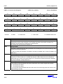
REVISION DESCRIPTIONS (REV 1.00)
Chapter
Chapter Name
−
Page
−
Subjects (Major changes comparing with last version)
−
Table of Contents
Chapter 1
Product Overview
1. Overview ..................................................................................................................................................1-1
1.1 Introduction .....................................................................................................................................1-1
2. Features ...................................................................................................................................................1-2
3. Block Diagram ..........................................................................................................................................1-3
4. Pin Assignments.......................................................................................................................................1-4
5. Pin Descriptions .......................................................................................................................................1-9
6. Memory Address ......................................................................................................................................1-12
Chapter 2
A/D Converter
1. Overview ..................................................................................................................................................2-1
1.1 Features..........................................................................................................................................2-1
2. Block Diagram ..........................................................................................................................................2-2
3. A/D Converter Operation..........................................................................................................................2-3
3.1 Function Description .......................................................................................................................2-3
4. Registers Description ...............................................................................................................................2-7
Chapter 3
Basic Timer & Watchdog Timer
1. Overview ..................................................................................................................................................3-1
2. Function Description.................................................................................................................................3-2
2.1 Interval Timer Function ...................................................................................................................3-2
2.2 Watchdog Timer Operation ............................................................................................................3-3
2.3 Timer Duration ................................................................................................................................3-4
2.4 Watch Dog Timer Duration .............................................................................................................3-5
3. Registers Description ...............................................................................................................................3-6
S3F401F_UM_REV1.00 MICROCONTROLLER
iii
Table of Contents (Continued)
Chapter 4
Encoder Counter
1. Overview.................................................................................................................................................. 4-1
2. Function Description ................................................................................................................................ 4-3
2.1 Position Counter Operation............................................................................................................ 4-3
3. Registers Description............................................................................................................................... 4-4
Chapter 5
Internal Flash ROM
1. Overview.................................................................................................................................................. 5-1
1.2 Features ......................................................................................................................................... 5-1
2. Block Diagram ......................................................................................................................................... 5-1
3. Flash Configuration.................................................................................................................................. 5-2
3.1 Flash ROM Configuration .............................................................................................................. 5-2
3.2 Address Alignment......................................................................................................................... 5-2
3.3 Working Mode ................................................................................................................................ 5-2
3.4 Program Mode ............................................................................................................................... 5-2
4. Programming Modes ............................................................................................................................... 5-3
4.1 User Program Mode....................................................................................................................... 5-3
4.2 Normal Program............................................................................................................................. 5-4
4.3 Option Program.............................................................................................................................. 5-5
4.4 Sector Erase .................................................................................................................................. 5-6
4.5 Chip Erase Flowchart..................................................................................................................... 5-7
4.6 Tool Program Mode ....................................................................................................................... 5-8
5. Data Protection ........................................................................................................................................ 5-9
5.1 Protection Option Configuration..................................................................................................... 5-9
5.2 Jtag Interface Protection Bit 8........................................................................................................ 5-10
5.3 Hardware Protection Bit 17 ............................................................................................................ 5-10
5.4 Read Protection Bit 27 ................................................................................................................... 5-11
6. Registers Description............................................................................................................................... 5-12
iv
S3F401F_UM_REV1.00 MICROCONTROLLER
Table of Contents (Continued)
Chapter 6
Inverter Motor Controller (IMC)
1. Overview ..................................................................................................................................................6-1
2. Block Diagram ..........................................................................................................................................6-2
3. Function Description.................................................................................................................................6-3
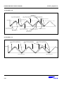
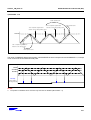
3.1 Tri-Angular Wave............................................................................................................................6-3
3.2 Saw-Tooth Wave ............................................................................................................................6-4
4. Phase Signal Generation .........................................................................................................................6-5
4.1 Tri-Angular Wave (IMMODE = 0) ...................................................................................................6-5
4.2 Tri-Angular Wave (IMMODE = 0) ...................................................................................................6-7
4.3 Tri-Angular Wave (IMMODE = 0) ...................................................................................................6-9
4.4 Tri-Angular Wave (IMMODE = 0) ...................................................................................................6-10
4.5 Tri-Angular Wave (IMMODE = 0) ...................................................................................................6-11
4.6 Tri-Angular Wave (IMMODE = 0) ...................................................................................................6-13
4.7 Tri-Angular Wave (IMMODE = 0) ...................................................................................................6-14
4.8 Tri-Angular Wave (IMMODE = 0) ...................................................................................................6-15
4.9 Saw-Tooth Wave (IMMODE = 1)....................................................................................................6-16
4.10 Saw-Tooth Wave (IMMODE = 1)..................................................................................................6-19
4.11 Saw-Tooth Wave (IMMODE = 1)..................................................................................................6-20
4.12 Saw-Tooth Wave (IMMODE = 1)..................................................................................................6-21
4.13 Saw-Tooth Wave (IMMODE = 1)..................................................................................................6-22
4.14 Saw-Tooth Wave (IMMODE = 1)..................................................................................................6-23
4.15 Saw-Tooth Wave (IMMODE = 1)..................................................................................................6-24
4.16 Saw-Tooth Wave (IMMODE = 1)..................................................................................................6-25
5. Inverter Motor Special Function Register.................................................................................................6-26
Chapter 7
Interrupt Controller
1. Overview ..................................................................................................................................................7-1
2. Functional Description..............................................................................................................................7-3
2.1 Configuring IRQ and FIQ Interrupt Service ....................................................................................7-3
2.2 Interrupt Registers ..........................................................................................................................7-3
2.3 Interrupt Sources ............................................................................................................................7-5
3. Registers Description ...............................................................................................................................7-8
S3F401F_UM_REV1.00 MICROCONTROLLER
v
Table of Contents (Continued)
Chapter 8
I/O Ports
1. Overview.................................................................................................................................................. 8-1
2. S3F401F Port Configuration Overview.................................................................................................... 8-2
3. I/O Port Control Registers ....................................................................................................................... 8-3
4. Registers Description............................................................................................................................... 8-4
Chapter 9
Clock & Power Management
1. Overview.................................................................................................................................................. 9-1
2. Phase Locked Loop................................................................................................................................. 9-4
2.1 PLL................................................................................................................................................. 9-4
2.2 PLL Value Change Steps............................................................................................................... 9-5
2.3 Capacitor for PLL Loop Filter ......................................................................................................... 9-5
3. Mode Change .......................................................................................................................................... 9-6
3.1 Changing clock speed from normal mode to highspeed mode [NORMAL Æ HIGHSPEED] ........ 9-6
3.2 Changing clock speed from highspeed mode to normal mode [HIGHSPEED Æ NORMAL] ........ 9-6
3.3 Entering the stop mode from high speed mode [HIGHSPEED Æ STOP] ..................................... 9-6
3.4 Exit From the STOP mode............................................................................................................. 9-6
3.5 Exit From the Clock fail mode ........................................................................................................ 9-6
3.6 IDLE Mode and Internal Flash ROM.............................................................................................. 9-6
4. Registers Description............................................................................................................................... 9-7
vi
S3F401F_UM_REV1.00 MICROCONTROLLER
Table of Contents (Continued)
Chapter 10
SSP (Synchronous Serial Port)
1. Overview ..................................................................................................................................................10-1
1.1 Features..........................................................................................................................................10-1
1.2 Programmable Parameters ............................................................................................................10-1
2. Block Diagram ..........................................................................................................................................10-2
2.1 SSP Functional Description............................................................................................................10-3
2.2 Frame Format .................................................................................................................................10-6
2.3 Interrupt ..........................................................................................................................................10-13
3. Registers Description ...............................................................................................................................10-14
Chapter 11
16-Bit Timers
1. Overview ..................................................................................................................................................11-1
2. Operation Description...............................................................................................................................11-3
2.1 Interval Mode Operation .................................................................................................................11-3
2.2 Match & Overflow Mode Operation ................................................................................................11-4
2.3 Capture Mode Operation ................................................................................................................11-5
2.4 PWM Mode Operation ....................................................................................................................11-6
S3F401F_UM_REV1.00 MICROCONTROLLER
vii
Table of Contents (Continued)
Chapter 12
UART
1. Overview.................................................................................................................................................. 12-1
1.1 The Uart Performs: ........................................................................................................................ 12-1
1.2 IrDA SIR Block ............................................................................................................................... 12-2
1.3 Features ......................................................................................................................................... 12-2
1.4 Programmable Parameters............................................................................................................ 12-3
1.5 Variations from the 16C550 Uart ................................................................................................... 12-4
2. Block Diagram ......................................................................................................................................... 12-5
3. Function Description ................................................................................................................................ 12-6
3.1 Baud Rate Generator..................................................................................................................... 12-6
3.2 Transmit FIFO ................................................................................................................................ 12-7
3.3 Transmit Logic................................................................................................................................ 12-7
3.4 Receive FIFO ................................................................................................................................. 12-7
3.5 Receive Logic................................................................................................................................. 12-7
3.6 Uart Operation................................................................................................................................ 12-7
3.7 IrDA SIR Operation ........................................................................................................................ 12-9
3.8 Interrupts ........................................................................................................................................ 12-11
4. Registers Description............................................................................................................................... 12-14
Chapter 13
Electrical Data
1. DC Electrical Characteristics ................................................................................................................... 13-1
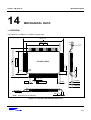
Chapter 14
Mechanical Data
1. Overview.................................................................................................................................................. 14-1
viii
S3F401F_UM_REV1.00 MICROCONTROLLER
List of Figures
Figure
Number
Title
Page
Number
1-1
1-2
S3F401F Block Diagram..............................................................................................1-3
S3F401F Package Pin Assignments (100-QFP-1420) ................................................1-4
2-1
2-2
A/D Converter Block Diagram......................................................................................2-2
ADC Operation Flow Chart ..........................................................................................2-6
3-1
Basic Timer Block Diagram..........................................................................................3-1
4-1
4-2
Encoder Counter Block Diagram .................................................................................4-2
Position Counter Operation..........................................................................................4-3
5-1
5-2
5-3
5-4
5-5
Flash Memory Controller Read/Write Block Diagram ..................................................5-1
Normal Program Flowchart ..........................................................................................5-4
Option Program Flowchart ...........................................................................................5-5
Sector Erase Flowchart................................................................................................5-6
Chip Erase Flowchart...................................................................................................5-7
6-1
6-2
6-3
6-4
Inverter Motor Controller (IMC) Block Diagram ...........................................................6-2
Inverter Motor Controller (IMC) Signal generation (Tri-angular wave) ........................6-3
Inverter Motor Controller (IMC) Signal generation (Saw-tooth wave)..........................6-4
Inverter Motor Controller (IMC) Signal generation (Tri-angular wave) ........................6-5
7-1
S3F401F Interrupt Structure ........................................................................................7-2
9-1
9-2
9-3
9-4
Clock State Machine Diagram .....................................................................................9-2
Clock Circuit Diagram ..................................................................................................9-3
PLL (Phase-Locked Loop) Block Diagram...................................................................9-5
Capacitor for PLL Loop Filter .......................................................................................9-5
S3F401F_UM_REV1.00 MICROCONTROLLER
ix
List of Figures (Continued)
Figure
Number
Title
Page
Number
10-1
10-2
10-3
10-4
10-5
10-6
10-7
10-8
10-9
10-10
SSP Block Diagram ..................................................................................................... 10-2
SUB Block Diagram..................................................................................................... 10-3
SSP frame format (single transfer) with SPO=0 and SPH=0...................................... 10-7
SSP frame format (continuous transfer) with SPO=0 and SPH=0.............................. 10-7
SSP frame format with SPO=0 and SPH=1 ................................................................ 10-8
SSP frame format (single transfer) with SPO=1 and SPH=0...................................... 10-9
SSP frame format (continuous transfer) with SPO=1 and SPH=0.............................. 10-9
SSP Frame Format with SPO=1 and SPH=1.............................................................. 10-10
PrimeCell SSP Master Coupled to Two Slaves .......................................................... 10-11
SPI master coupled to two PrimeCell SSP slaves ...................................................... 10-12
11-1
11-2
11-3
11-4
11-5
11-6
16-Bit Timer Block Diagram ........................................................................................ 11-2
Simplified Timer Function Diagram: Interval Timer Mode ........................................... 11-3
Simplified Timer Function Diagram: Match & Overflow Timer Mode .......................... 11-4
Simplified Timer Function Diagram: Capture Mode .................................................... 11-5
Simplified Timer Function Diagram: PWM Mode ........................................................ 11-6
PWM Signal Generation Diagram ............................................................................... 11-7
12-1
12-2
12-3
UART Block Diagram (with FIFO) ............................................................................... 12-5
UART character frame ................................................................................................ 12-7
IrDA data modulation................................................................................................... 12-10
13-1
13-2
ADC Offset Error ......................................................................................................... 13-6
ADC DLE, ILE.............................................................................................................. 13-7
14-1
100-QFP-1420 Package Dimensions.......................................................................... 14-1
x
S3F401F_UM_REV1.00 MICROCONTROLLER
List of Tables
Table
Number
Title
Page
Number
1-1
1-2
1-3
1-4
Pin Assignments − Pin Number Order .........................................................................1-5
S3F401F Pin Descriptions ...........................................................................................1-9
S3F401F Default Memory Map after Reset .................................................................1-12
The Base Address of Peripheral Special Registers.....................................................1-13
2-1
2-2
ADC Input & Output Range..........................................................................................2-3
ADC Control Special Function Registers .....................................................................2-7
3-1
Basic timer & WDT Special Function Registers...........................................................3-6
4-1
ENC Special Function Registers..................................................................................4-4
5-1
5-2
5-3
5-4
5-5
The Pins Used to Read/Write/Erase the Flash ROM in Tool Program Mode..............5-8
Protection Option Address and Protection Bits............................................................5-9
Smart Option Address Configuration ...........................................................................5-10
Hardware Protection Area............................................................................................5-11
Internal Flash Special Function Registers ...................................................................5-12
6-1
IMC Special Function Registers...................................................................................6-25
7-1
7-2
S3F401F Interrupt Sources..........................................................................................7-5
Interrupt Controller Special Function Registers ...........................................................7-8
8-1
8-2
S3F401F Port Configuration Overview ........................................................................8-2
Port Control Special Function Registers ......................................................................8-4
9-1
9-2
Clock & Power Management Special Function Register .............................................9-7
MDIV/PDIV/SDIV Allowed Values................................................................................9-11
10-1
10-2
UART Interrupts In Connection With FIFO ..................................................................10-13
Clock & Power Management Special Function Register .............................................10-14
11-1
TIMER Special Function Registers ..............................................................................11-8
12-1
UART Special Function Registers ...............................................................................12-14
13-1
13-2
13-3
13-4
13-5
13-6
13-7
13-8
Absolute Maximum Ratings .........................................................................................13-1
D.C. Electrical Characteristics .....................................................................................13-2
Timing Constants .........................................................................................................13-3
PLL Timing Constants..................................................................................................13-3
Internal RC Oscillation Characteristics ........................................................................13-4
AC Electrical Characteristics........................................................................................13-4
12-bit ADC Electrical Characteristics ...........................................................................13-5
AC Electrical Characteristics for Internal Flash ROM ..................................................13-8
S3F401F_UM_REV1.00 MICROCONTROLLER
xi
S3F401F_UM_REV1.00
1
PRODUCT OVERVIEW
PRODUCT OVERVIEW
1. OVERVIEW
1.1 INTRODUCTION
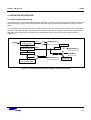
Samsung's S3F401F 16/32-bit RISC microcontroller is a cost-effective and high-performance microcontroller
solution for an inverter motor and a general-purpose application.
An outstanding feature of the S3F401F is its CPU core, a 16/32-bit RISC processor (ARM7TDMI-S) designed by
Advanced RISC Machines, Ltd. The ARM7TDMI-S core is a low-power, general purpose, microprocessor macrocell, which was developed for the use in application-specific and customer-specific integrated circuits. Its simple,
elegant, and fully static design is particularly suitable for cost-sensitive and power-sensitive application. Using the
ARM7TDMI-S core, CMOS standard cell, and a data path compiler has developed the S3F401F. Most of the onchip function blocks have been designed using an HDL synthesizer
The integrated on-chip functions, which are described in this document include:
• Built-in 256Kbyte NOR-Flash memory
• Internal 20Kbyte SRAM for stack, data memory, or code memory
• Interrupt controller: 90 interrupt sources, interrupt priority control logic and interrupt vector generation by H/W.
• Three programmable I/O port groups
• Two inverter timer, Two channel 16bit encoder counter, having PHASE A,B and Z
• Two-channel UART, Two-channel SSP
• Six-channel 16-bit timers with capture and PWM
• Fifteen-channel 12-bit ADC
• One-channel 8-bit basic timer and 3-bit watch-dog timer
• Crystal/Ceramic oscillator or external clock can be used as the clock source and PLL
• Power control: Normal, Idle, and Stop mode
• Clock monitor
1-1
PRODUCT OVERVIEW
S3F401F_UM_REV1.00
2. FEATURES
CPU
Two Channels UART
•
•
•
ARM7TDMI-S CPU Core
32-bit RISC architecture
Memory
•
•
•
256 Kbytes Internal Program Full Flash
20 Kbytes Internal SRAM
Only little-endian support
•
•
•
•
Programmable use of UART or IrDA SIR input
/output
Separate 16x8bit transmit and 16x12bit receive
FIFO
Programmable baud rate generator
Standard asynchronous communication bits
(start, stop, parity)
Auto generating parity bit
General purpose I/O Pins
Analog to Digital Converter
•
•
•
Max. 65 pins
31 external interrupts
•
•
15-channel analog inputs
12-bit resolution
Simultaneous Sampling of 3 Single-Ended
8-Bit Basic Timer
Interrupt Controller
•
•
•
Programmable interval timer
Watch-dog timer’s clock source, overflow of 8-bit
counter
Watchdog Timer
•
•
•
Supports normal or fast interrupt modes
(IRQ, FIQ)
Supports vectored interrupt
(Hard-wired Interrupt)
S/W programmable interrupt priority
System reset when 3-bit counter overflow
Two Power-Down Modes
Six 16-bit Timer/Counters (T/C0 - T/C5)
•
•
•
Programmable interval timer
External event counter function
PWM function and capture function
•
•
Clock Manager (CM)
•
Two Inverter Motor Controllers
•
•
•
3-Phase pairs’ PWM generation
Programmable dead time insertion
ADC conversion start signal generation
Idle: only CPU clock stops
Stop: selected system clock and CPU clock stop
CPU and peripherals can be deactivated
individually
Phase-Locked Loop (PLL)
•
Programmable clock synthesizer (Max 90MHz)
Two 16-Bit Encoder Counter
Operating Voltage Range
•
•
•
•
•
Support position counter and speed counter
Up/Down counter
3 inputs, Phase A,B and Z
Capture mode support
Two channel 16-Bit Synchronous Serial Port
•
•
•
•
1-2
Master or slave operation
Programmable clock bit rate and pre-scale
Separate 8x16bit transmit/receive FIFO
4 to 16-bit transmit/receive mode
3.0 V to 3.6 V at 4.0MHz − 90.0MHz
(external crystal: 4.0MHz − 8MHz)
Power-On Reset (POR)
•
Clock Monitor
Operating Temperature Range
•
−40°C to +85°C
Available in 100 QFP Package
S3F401F_UM_REV1.00
PRODUCT OVERVIEW
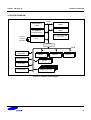
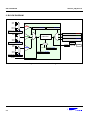
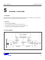
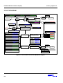
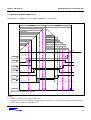
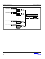
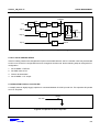
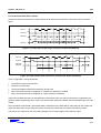
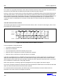
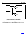
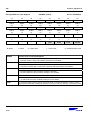
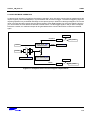
3. BLOCK DIAGRAM
AHB
FLASH-ROM
256KB
ARM7TDMI-S
CORE
SRAM
20KB
INTERRUPT
CONTROLLER
Crystal or
Ceramic
Oscillator
TAP CONTROLLER
For JTAG
PLL
BRIDGE
APB
CLOCK
MONITOR
I/O
CONTROLLER
IMC0/1
IMC0/1
ENC0/1
ENC0/1
UART0/1
UART0/1
SSP0/1
SSP0/1
BT & WDT
12-BIT ADC
Timer0/1/2/3/4/5
Timer0/1/2/3/4/5
Timer0/1/2/3/4/5
Timer0/1/2/3/4/5
TIMER 0/1/2/3/4/5
Figure 1-1. S3F401F Block Diagram
1-3
PRODUCT OVERVIEW
S3F401F_UM_REV1.00
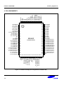
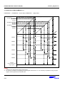
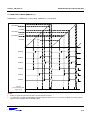
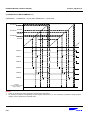
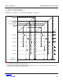
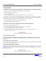
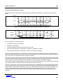
100
99
98
97
96
95
94
93
92
91
90
89
88
87
86
85
84
83
82
81
nRESET
RTCK
TMS
TDI
TCK
TDO
nTRST
VDDIO2
VSSIO2
PLLVSSIP
PLLVDDOUT
PLLVDDCORE
PLLCAP
PLLVSSCORE
ADCVSSCORE
ADCVDDCORE
ADCVSSIO
ADCVDDIO
P2.14/AIN14
P2.13/AIN13
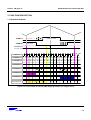
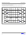
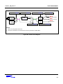
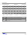
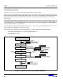
4. PIN ASSIGNMENTS
1
2
3
4
5
6
7
8
9
10
11
12
13
14
15
16
17
18
19
20
21
22
23
24
25
26
27
28
29
30
S3F401F
(100-QFP-1420C)
80
79
78
77
76
75
74
73
72
71
70
69
68
67
66
65
64
63
62
61
60
59
58
57
56
55
54
53
52
51
P2.12/AIN12
P2.11/AIN11
P2.10/AIN10
P2.9/AIN9
P2.8/AIN8
P2.7/AIN7
P2.6/AIN6
P2.5/AIN5
P2.4/AIN4
P2.3/AIN3
P2.2/AIN2
P2.1/AIN1
P2.0/AIN0
VSSCORE2
VDDCORE2
P1.30/PWM1D2/INT30
P1.29/PWM1U2/INT29
P1.28/PWM1D1/INT28
P1.27/PWM1U1/INT27
P1.26/PWM1D0/INT26
P1.25/PWM1U0/INT25
P1.24/PWM1OFF/INT24
P1.23/PHASEZ1/INT23
P1.22/PHASEB1/INT22
P1.21/PHASEA1/INT21
P1.20/SSPFSS1/INT20
P1.19/SSPCLK1/INT19
P1.18/SSPRXD1/INT18
P1.17/SSPTXD1/INT17
MD2
VSSIO0
VDDIO0
VSSIP
P1.7/T4CLK/INT7
P1.8/T4CAP/INT8
P1.9/T4PWM/INT9
P1.10/T5CLK/INT10
P1.11/P5CAP/INT11
P1.12/T5PWM/INT12
VDDOUT
VSSCORE1
VDDCORE1
VSSIO1
VDDIO1
P1.13/SSPTXD0/INT13
P1.14/SSPRXD0/INT14
P1.15/SSPCLK0/INT15
P1.16/SSPFSS0/INT16
MD0
MD1
31
32
33
34
35
36
37
38
39
40
41
42
43
44
45
46
47
48
49
50
P0.0/T0CLK
P0.1/T0CAP
P0.2/T0PWM
P0.3/T1CLK
P0.4/T1CAP
P0.5/T1PWM
P0.6/T2CLK
P0.7/T2CAP
P0.8/T2PWM/ADTRG
P0.9/PHASEA0
P0.10/PHASEB0
P0.11/PHASEZ0
Xin
Xout
VSSCORE0
VDDCORE0
P0.12/PWM0OFF
P0.13/PWM0U0
P0.14/PMW0D0
P0.15/PMW0U1
P0.16/PWM0D1
P0.17/PWM0U2
P0.18/PMW0D2
P1.0/UARTRXD0/INT0
P1.1/UARTTXD0/INT1
P1.2/UARTRXD1/INT2
P1.3/UARTTXD1/INT3
P1.4/T3CLK/INT4
P1.5/T3CAP/INT5
P1.6/T3PWM/INT6
Figure 1-2. S3F401F Package Pin Assignments (100-QFP-1420)
1-4
S3F401F_UM_REV1.00
PRODUCT OVERVIEW
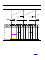
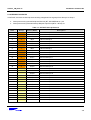
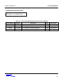
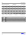
Table 1-1. Pin Assignments − Pin Number Order
No.
Pin Name
Default Function State
Flash Function
1
P0.0
T0CLK
−
P0.2
I/O
−
2
P0.1
T0CAP
−
P0.1
I/O
−
3
P0.2
T0PWM
−
P0.2
I/O
−
4
P0.3
T1CLK
−
P0.3
I/O
−
5
P0.4
T1CAP
−
P0.4
I/O
−
6
P0.5
T1PWM
−
P0.5
I/O
−
7
P0.6
T2CLK
−
P0.6
I/O
−
8
P0.7
T2CAP
−
P0.7
I/O
−
9
P0.8
T2PWM
ADTRG
P0.8
I/O
−
10
P0.9
PHASEA0
−
P0.9
I/O
−
11
P0.10
PHASEB0
−
P0.10
I/O
−
12
P0.11
PHASEZ0
−
P0.11
I/O
−
13
Xin
−
−
Xin
I
−
14
Xout
−
−
Xout
O
−
15
VSSCORE0
−
−
VSS
P
−
16
VDDCORE0
−
−
VDD
P
−
17
P0.12
PWM0OFF
−
P0.12
I/O
−
18
P0.13
PWM0U0
−
P0.13
I/O
−
19
P0.14
PMW0D0
−
P0.14
I/O
−
20
P0.15
PMW0U1
−
P0.15
I/O
−
21
P0.16
PWM0D1
−
P0.16
I/O
−
22
P0.17
PWM0U2
−
P0.17
I/O
−
23
P0.18
PMW0D2
−
P0.18
I/O
−
24
P1.0
UARTRXD0
INT0
P1.0
I/O
−
25
P1.1
UARTTXD0
INT1
P1.1
I/O
−
26
P1.2
UARTRXD1
INT2
P1.2
I/O
−
27
P1.3
UARTTXD1
INT3
P1.3
I/O
−
28
P1.4
T3CLK
INT4
P1.4
I/O
−
29
P1.5
T3CAP
INT5
P1.5
I/O
−
30
P1.6
T3PWM
INT6
P1.6
I/O
−
1-5
PRODUCT OVERVIEW
S3F401F_UM_REV1.00
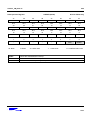
Table 1-1. Pin Assignments − Pin Number Order (Continued)
No.
1-6
Pin Name
Default Function State
Flash Function
31
VSSIO0
−
−
VSS
P
−
32
VDDIO0
−
−
VDD
P
−
33
VSSIP
−
−
VSS
P
−
34
P1.7
T4CLK
INT7
P1.7
I/O
−
35
P1.8
T4CAP
INT8
P1.8
I/O
−
36
P1.9
T4PWM
INT9
P1.9
I/O
−
37
P1.10
T5CLK
INT10
P1.10
I/O
−
38
P1.11
T5CAP
INT11
P1.11
I/O
−
39
P1.12
T5PWM
INT12
P1.12
I/O
−
40
VDDOUT
−
−
VDDOUT
P
−
41
VSSCORE1
−
−
VSS
P
−
42
VDDCORE1
−
−
VDD
P
−
43
VSSIO1
−
−
VSS
P
−
44
VDDIO1
−
−
VDD
P
−
45
P1.13
SSPTXD0
INT13
P1.13
I/O
−
46
P1.14
SSPRXD0
INT14
P1.14
I/O
−
47
P1.15
SSPCLK0
INT15
P1.15
I/O
SDAT (I/O)
48
P1.16
SSPFSS0
INT16
P1.16
I/O
SCLK (I)
49
MD0
−
−
MD0
I
MD0
50
MD1
−
−
MD1
I
MD1
S3F401F_UM_REV1.00
PRODUCT OVERVIEW
Table 1-1. Pin Assignments − Pin Number Order (Continued)
No.
Pin Name
Default Function State
Flash Function
51
MD2
−
−
MD2
I
MD2
52
P1.17
SSPTXD1
INT17
P1.17
I/O
−
53
P1.18
SSPRXD1
INT18
P1.18
I/O
−
54
P1.19
SSPCLK1
INT19
P1.19
I/O
−
55
P1.20
SSPFSS1
INT20
P1.20
I/O
−
56
P1.21/
PHASEA1
INT21
P1.21
I/O
−
57
P1.22
PHASEB1
INT22
P1.22
I/O
−
58
P1.23
PHASEZ1
INT23
P1.23
I/O
−
59
P1.24
PWM1OFF
INT24
P1.24
I/O
−
60
P1.25
PWM1U0
INT25
P1.25
I/O
−
61
P1.26
PWM1D0
INT26
P1.26
I/O
−
62
P1.27
PWM1U1
INT27
P1.27
I/O
−
63
P1.28/
PWM1D1
INT28
P1.28
I/O
−
64
P1.29
PWM1U2
INT29
P1.29
I/O
−
65
P1.30
PWM1D2
INT30
P1.30
I/O
−
66
VDDCORE2
−
−
VDD
P
−
67
VSSCORE2
−
−
VSS
P
−
68
P2.0
AIN0
−
P2.0
I/O
−
69
P2.1
AIN1
−
P2.1
I/O
−
70
P2.2
AIN2
−
P2.2
I/O
−
71
P2.3
AIN3
−
P2.3
I/O
−
72
P2.4
AIN4
−
P2.4
I/O
−
73
P2.5
AIN5
−
P2.5
I/O
−
74
P2.6
AIN6
−
P2.6
I/O
−
75
P2.7
AIN7
−
P2.7
I/O
−
76
P2.8
AIN8
−
P2.8
I/O
−
77
P2.9
AIN9
−
P2.9
I/O
−
78
P2.10
AIN10
−
P2.10
I/O
−
79
P2.11
AIN11
−
P2.11
I/O
−
80
P2.12
AIN12
−
P2.12
I/O
−
1-7
PRODUCT OVERVIEW
S3F401F_UM_REV1.00
Table 1-1. Pin Assignments − Pin Number Order (Continued)
No.
1-8
Pin Name
Default Function State
Flash Function
81
P2.13
AIN13
−
P2.13
I/O
–
82
P2.14
AIN14
−
P2.14
I/O
–
83
ADCVDDIO
−
−
VDD
P
–
84
ADCVSSIO
−
−
VSS
P
–
85
ADCVDDCORE
−
−
VDD
P
–
86
ADCVSSCORE
−
−
VSS
P
–
87
PLLVSSCORE
−
−
VSS
P
–
88
PLLCAP
−
−
PLLCAP
I
–
89
PLLVDDCORE
−
−
VDD
P
–
90
PLLVDDOUT
−
−
VDDPLLOUT
P
–
91
PLLVSSIP
−
−
VSS
P
–
92
VSSIO2
−
−
VSS
P
–
93
VDDIO2
−
−
VDD
P
–
94
nTRST
−
−
nTRST
I
–
95
TDO
−
−
TDO
O
–
96
TCK
−
−
TCK
I
–
97
TDI
−
−
TDI
I
–
98
TMS
−
−
TMS
I
–
99
RTCK
−
−
RTCK
O
–
100
nRESET
−
−
nRESET
I
nRESET
S3F401F_UM_REV1.00
PRODUCT OVERVIEW
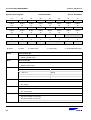
5. PIN DESCRIPTIONS
Table 1-2. S3F401F Pin Descriptions
Module
Pin Name
BUS
CONTROLLER
MD[2:0]
Description
The MD[2:0] can configure the operating mode of chip.
I/O
I
000 = Normal mode
001 = SPGM mode (Flash programming mode with writing tool)
Others = Test mode
Connect to GND through a 100nF capacitor with each mode
pin.
INTERRUPT
CLOCK &
RESET
INT[30:0]
Xin
Xout
PLLCAP
External interrupt request 31 to 0.
I
Crystal input of oscillator circuit for system clock.
I
Crystal output of oscillator circuit for system clock.
O
Capacitor for PLL loop filter.
I
Connect to GND through a 1200pF capacitor
nRESET
16-BIT TIMER
UART
SSP
ADC
Reset input: The global system reset input for the S3F401F.
For a system initialization, nRESET must be held to LOW level
for at least 1uSec. Connect to GND through 100nF and 10nF
capacitor.
I
T[5:0]CLK
External clock input for Timer
I
T[5:0]CAP
Capture input for Timer
I
T[5:0]PWM
PWM output for Timer
O
UARTRXD[1:0]
UART receive
I
UARTTXD[1:0]
UART transmit
O
SSPRXD[1:0]
SSP receive
I
SSPTXD[1:0]
SSP transmit
O
SSPCLK[1:0]
SSP clock
I/O
SSPFSS[1:0]
SSP frame input (for slave) / slave select output (for master)
I/O
ADC input
AI
AIN[14:0]
ADTRG
ADC trigger input
I
1-9
PRODUCT OVERVIEW
S3F401F_UM_REV1.00
Table 1-2. S3F401F Pin Descriptions (Continued)
Module
Pin Name
Description
TOOL Program
SDAT
Serial Data pin (Output when reading, Input when writing)
Input & Push-pull output port can be assigned.
SCLK
Serial Clock, input only
I/O
I/O
I
Writer speed : Max 250kHz, Read speed: Max 3MHz
JTAG
nTRST
nTRST (TAP Controller Reset) can reset the TAP controller at
power-up. A 200K pull-up resistor is connected to nTRST pin,
internally. If the debugger is not used, nTRST pin should be
"Low" level or low active pulse should be applied before CPU
running. For example, nRESET signal can be tied with
nTRST.
I
TMS
TMS (TAP Controller Mode Select) can control the sequence
of the state diagram of TAP controller. A 200K pull-up resistor
is connected to TMS pin, internally.
I
TCK
TCK (TAP Controller Clock) can provide the clock input for the
JTAG logic. This pin is floating pin. When reduced the current
and not debugging mode, connect to the VDD with pull-up
resistor.
I
RTCK (TAP Controller Retiming Clock) can provide the clock
output for the JTAG logic.
I
RTCK
Connect to GND through a 33pF capacitor.
INVERTER
MOTOR
CONTROLLER
ENCODER
GERNAL
PURPOSE
PORT
1-10
TDI
TDI (TAP Controller Data Input) is the serial input for JTAG
port. A 200K pull-up resistor is connected to TDI pin,
internally.
I
TDO
TDO (TAP Controller Data Output) is the serial output for
JTAG port.
O
PWM[1:0]U[2:0]
PWM output for inverter motor
O
PWM[1:0]D[2:0]
PWM output for inverter motor
O
PWM[1:0]OFF
Input pin for PWM output off
I
PHASEA[1:0]
Phase A input pin
I
PHASEB[1:0]
Phase B input pin
I
PHASEZ[1:0]
Phase Z input pin
I
P0.[18:0]
General input/output port 0
I/O
P1.[30:0]
General input/output port 1
I/O
P2.[14:0]
General input/output port 2
I/O
S3F401F_UM_REV1.00
PRODUCT OVERVIEW
Table 1-2. S3F401F Pin Descriptions (Continued)
Module
Pin Name
POWER
VDDCORE[2:0]
Core logic VDD (Typ. 3.3V)
P
VSSCORE[2:0]
Core logic VSS
P
I/O VDD (Typ. 3.3V)
P
VDDIO[2:0]
Description
I/O
Connect to GND through a 100nF capacitor.
I/O VSS
P
VSS
P
ADCVDDCORE
ADC Core logic VDD (Typ. 3.3V)
P
ADCVSSCORE
ADC Core logic VSS
P
ADCVDDIO
ADC I/O VDD (Typ. 3.3V)
P
ADCVSSIO
ADC I/O VSS
P
PLL Core logic VDD (Typ. 3.3V)
P
VSSIO[2:0]
VSSIP
PLLVDDCORE
Connect to GND through a 100nF capacitor.
PLL Core logic VSS
P
VSS
P
PLLVDDOUT
Connect to GND through a 1uF capacitor (From internal regulator)
P
VDDOUT
Connect to GND through a 1uF capacitor (From internal regulator)
P
PLLVSSCORE
PLLVSSIP
1-11
PRODUCT OVERVIEW
S3F401F_UM_REV1.00
6. MEMORY ADDRESS
When the reset of S3F401F micro-controller is asserted, the ARM core is in boot mode to access the internal flash
at address 0x00000000. The internal RAM is located at address 0x00400000.
Table 1-3. S3F401F Default Memory Map after Reset
1-12
Memory Space
Size
Application
Abort when Accessed
0xFFFFFFFF
−
0xFF000000
−
Peripheral devices
No
0xFEFFFFFF
−
0x00405000
−
Reserved
Yes
0x00404FFF
−
0x00400000
20Kbytes
Internal RAM
No
0x003FFFFF
−
0x00040000
−
Reserved
Yes
0x0003FFFF
−
0x00000000
256Kbytes
Internal flash
No
S3F401F_UM_REV1.00
PRODUCT OVERVIEW
Table 1-4. The Base Address of Peripheral Special Registers
Peripheral
Base Address
CM
0xFF00_0000
BT/WDT
0xFF00_4000
TC0
0xFF00_8000
TC1
0xFF00_C000
TC2
0xFF01_0000
TC3
0xFF01_4000
TC4
0xFF01_8000
TC5
0xFF01_C000
IMC0
0xFF02_0000
IMC1
0xFF02_4000
ENC0
0xFF02_8000
ENC1
0xFF02_C000
SSP0
0xFF03_0000
SSP1
0xFF03_4000
UART0
0xFF03_8000
UART1
0xFF03_C000
ADC
0xFF04_0000
IOPORT
0xFF04_4000
IFC
0xFFF0_0000
VIC
0xFFFF_FF00
1-13
S3F401F_UM_REV1.00
2
A/D CONVERTER
A/D CONVERTER
1. OVERVIEW
The S3F401F has a 12-bit ADC. It converts the analog input signal into 12-bit binary digital codes at a maximum
sampling rate of 4MHz. The device is a monolithic ADC with on-chip, which consists of three sample and hold
amplifiers, four multiplying DACs, five sub-ranging flash ADCs and current reference. Normal speed of input is
below 100kHz which can be quantized by 4MHz clock.
1.1 FEATURES
•
ADC Resolution: 12-bit
•
DLE (Differential Linearity Error): Max. ± 1.0 LSB (Least Bit)
•
ILE (Integral Linearity Error): Max. ± 3.2 LSB
•
Maximum Conversion Rate: 4MHz clock
•
Low Power Consumption
•
Power Supply Voltage: 3.3V
•
Analog Input Range: 0.0V ∼ 3.3V
2-1
A/D CONVERTER
S3F401F_UM_REV1.00
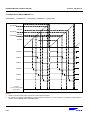
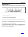
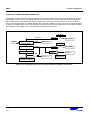
2. BLOCK DIAGRAM
AIN0
AIN1
SHA1
AIN13
AIN14
ADCCON.9-.8:MODESEL
ADCCON.9-.8:MODESEL
ADCCON.15-.12: SHA1SEL
ADCRESULT1.11-.0 : DATA1
AIN0
AIN1
SHA2
12bit ADC
ADCRESULT2.11-.0 : DATA2
ADCRESULT3.11-.0 : DATA3
AIN13
AIN14
INTMASK
ADCCON.19-.16:SHA2SEL
AIN0
AIN1
AIN13
AIN14
INTPND
SHA3
From IMC ADCCON.0:START
ADCCON.3-.2:TRIGSEL
ADCCON.23-.20:SHA3SEL
ADTRG
Figure 2-1. A/D Converter Block Diagram
2-2
INT_EOC
S3F401F_UM_REV1.00
A/D CONVERTER
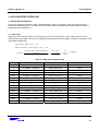
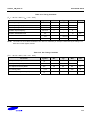
3. A/D CONVERTER OPERATION
3.1 FUNCTION DESCRIPTION
ADC has 3-analog input channels, SHA1, SHA2 and SHA3. After 3 conversion of ADC, the result of SHA1 is
pushed into the ADCRESULT1, the result of SHA2 is pushed into the ADCRESULT2 and the result of SHA3 is
pushed into the ADCRESULT3.
3.1.1 ADC Input
AIN[14:0] function pins are used for an analog input source to convert by ADC. ADC 3-input channels can be
selected one among AIN[14:0] inputs. Input signal range is followed by the boundary of reference, Reference TOP
and Reference BOTTOM.
Input Voltage Range: 0.0V ~ 3.3V
Reference Bottom = 0.0V, Reference Top = 3.3V
1 LSB
=
Reference Top - Reference Bottom
2
Resolution
=
3.3V - 0.0V
2
12
=
3.3V
4096
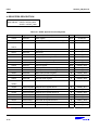
= 0.806mV
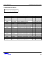
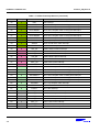
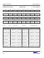
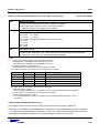
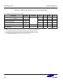
Table 2-1. ADC Input & Output Range
Index
SHA1, SHA2, SHA3 Input (V)
Digital Output (Binary)
Digital Output (HEX)
0
0.000000 ~ 0.000806
0000_0000_0000
0x000
1
0.000806 ~ 0.001612
0000_0000_0001
0x001
2
0.001612 ~ 0.002418
0000_0000_0010
0x002
•••
•••
•••
•••
1239
0.998634 ~ 0.999440
0100_1101_0111
0x4D7
1240
0.999440 ~ 1.000246
0100_1101_1000
0x4D8
1241
1.000246 ~ 1.001052
0100_1101_1001
0x4D9
•••
•••
•••
•••
2047
1.649194 ~ 1.650000
0111_1111_1111
0x7FF
2048
1.650000 ~ 1.650806
1000_0000_0000
0x800
2049
1.650806 ~ 1.651612
1000_0000_0001
0x801
•••
•••
•••
•••
4093
3.297582 ~ 3.298388
1111_1111_1101
0xFFD
4094
3.298388 ~ 3.299194
1111_1111_1110
0xFFE
4095
3.299194 ~ 3.300000
1111_1111_1111
0xFFF
2-3
A/D CONVERTER
S3F401F_UM_REV1.00
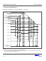
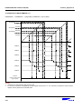
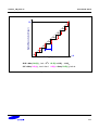
3.1.2 A/D Conversion
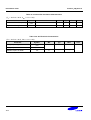
3.1.2.1 The Sampling Mode
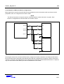
S3F401F′s ADC can get the result of maximum 3 converted digital data at one time. In other means, user can get
the AD conversion data one, two or three by one conversion. This is determined the ADC Mode Selection Bits in
ADCCON register.
MODESEL[1:0]
Description
Active Channel
0 0 ′b
3-point simultaneous sampling
SHA1
SHA2
SHA3
0 1 ′b
1-point sampling
SHA1
−
−
1 0 ′b
2-point simultaneous sampling
SHA1
SHA2
−
1 1 ′b
Reserved
−
−
−
3.1.2.2 The Conversion Start
The ADC conversion can be started by 3 triggered sources. Start trigger source is determined by TRIGSEL[1:0]
bits in ADCCON register. User should select the corresponding value each application.
a. Software Command
b. Inverter Motor Control Block (IMC) trigger signal
c. External Signal inserted into ADCTRG pin.
3.1.2.3 The End of Conversion
After finishing the conversion, user can catch the valid data by reading each result register. The end of conversion
is informed by the value of EOC bit in the interrupt pending register. So after ADC conversion, user should check
EOC pending bit and clear.
3.1.2.4 The Conversion Time
When the external/internal clock (Fin) frequency is 8MHz and the divider value is ‘1’ (Fin/2), total 12-bit conversion
time is as follows:
A/D converter clock = 8MHz / 2 = 4MHz
Conversion speed = 4MHz / 11cycles = 363.6 kHz → Conversion time = 2.75 us
NOTES:
1. This A/D converter was designed to operate at maximum 4MHz clock. If 1xchannel is selected for ADC conversion
(ADCCON.9-.8 = 01), maximum 9xclocks are needed for ADC conversion. If 2xchannels are selected for ADC conversion
(ADCCON.9-.8 = 10), maximum 10xclocks are needed for ADC conversion. If 3xchannels are selected for ADC
conversion (ADCCON.9-.8 = 00), maximum 11xclocks are needed for ADC conversion.
2. ADCCLK source is Fin, not PCLK. ADCCLK must be less than PCLK or equal.
2-4
S3F401F_UM_REV1.00
A/D CONVERTER
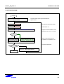
3.1.3 Standby Mode
Standby mode is activated when ADCCON.1 is set to '0'. In this mode, A/D conversion operation is halted and all
ADC result registers are set to ‘0’.
3.1.4 ADC Interrupt
The ADC generates an EOC interrupt when conversion is completed while ADC interrupt is enabled. You can
know if whether that interrupt occurs or not by reading the interrupt pending register. This interrupt bit can be
enabled or disabled using respectively the interrupt enable register and interrupt disable register.
NOTE
If you know whether an interrupt from ADC (EOC) occurs or not, read and check the EOC bit in the
interrupt pending register. It can cause the different result to read ADCSTATUS.0 (STATUS) bit to check
EOC interrupt.
2-5
A/D CONVERTER
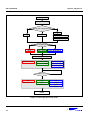
S3F401F_UM_REV1.00
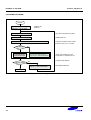
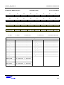
ADC Enable
ADC Clock Setting
Which ADC Trigger Source
ADCTRG
Software
IMC
ADCTRG Pin setting
EDGE Type Selection
Which Sampling Mode?
1-sampling
SHA1
2-sampling
SHA1, SHA2
3-sampling
SHA1,SHA2,SHA3
ADC START
Conversion SHA1
Conversion SHA1
Conversion SHA2
Conversion SHA1
Conversion SHA2
Conversion SHA3
EOC = '1' ?
read
ADCRESULT1
read
ADCRESULT1
read
ADCRESULT2
read
ADCRESULT1
read
ADCRESULT2
read
ADCRESULT3
STOP
Figure 2-2. ADC Operation Flow Chart
2-6
S3F401F_UM_REV1.00
A/D CONVERTER
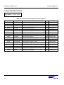
4. REGISTERS DESCRIPTION
Base Address − 0xFF04_0000
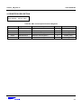
Table 2-2. ADC Control Special Function Registers
Offset Address
Register
0x000
ADCCON
0x004
Description
R/W
Reset Value
ADC control register
R/W
0x0000_0000
ADCSTATUS
ADC status register
R
0x0000_0000
0x008
ADCRESULT1
12bit ADC result register 1
R
0x0000_0000
0x00C
ADCRESULT2
12bit ADC result register 2
R
0x0000_0000
0x010
ADCRESULT3
12bit ADC result register 3
R
0x0000_0000
2-7
A/D CONVERTER
S3F401F_UM_REV1.00
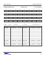
ADC Control Register
ADCCON (0x000)
Access: Read/Write
31
30
29
28
27
26
25
24
−
−
−
−
−
−
−
−
R/W-0
R/W-0
R/W-0
R/W-0
R/W-0
R/W-0
R/W-0
R/W-0
23
22
21
20
19
18
17
16
SHA3SEL [23:20]
SHA2SEL [17:16]
R/W-0
R/W-0
R/W-0
R/W-0
R/W-0
R/W-0
R/W-0
R/W-0
15
14
13
12
11
10
9
8
−
−
MODESEL[9:8]
SHA1SEL [15:12]
R/W-0
R/W-0
R/W-0
R/W-0
R/W-0
R/W-0
R/W-0
R/W-0
7
6
5
4
3
2
1
0
−
TRIGEDGESEL
EN
START
R/W-0
R/W-0
R/W-0
R/W-0
W: Write
R: Read
START
CLKSEL[5:4]
R/W-0
TRIGSEL[3:2]
R/W-0
-0: 0 After reset
R/W-0
-1: 1 After reset
R/W-0
-U: Undefined after reset
ADC Conversion Start Bit
0 = No effect
1 = Start
Note: This bit is auto-clear bit.
EN
ADC Block Enable Bit
0 = Disable
1 = Enable
TRIGSEL
ADC Start Trigger Signal Selection Field
00 = Software (By ADCCON.0)
01 = Inverter block
1x = ADCTRG pin
CLKSEL
ADC Clock (ADCCLK) Selection Field
000 = Fin
001 = Fin /2
010 = Fin /4
011 = Fin /8
Note: ADCCLK source is Fin, not PCLK, and ADCCLK is less than PCLK or equal.
TRIGEDGESEL
ADC Trigger Edge Selection Bit for ADTRG pin
0 = Falling edge
1 = Rising edge
2-8
S3F401F_UM_REV1.00
A/D CONVERTER
ADC Control Register (Continued)
MODESEL
ADCCON (0x000)
Access: Read/Write
ADC Mode Selection Field
00 = 3-point simultaneous sampling
01 = 1-point sampling
10 = 2-point simultaneous sampling
SHA1SEL
SHA2SEL
SHA3SEL
NOTE
ADC Input Selection Field for SHA1
0000 = AIN0
0101 = AIN5
1010 = AIN10
0001 = AIN1
0110 = AIN6
1011 = AIN11
0010 = AIN2
0111 = AIN7
1100 = AIN12
0011 = AIN3
1000 = AIN8
1101 = AIN13
0100 = AIN4
1001 = AIN9
1110 = AIN14
ADC Input Selection Field for SHA2
0000 = AIN0
0101 = AIN5
1010 = AIN10
0001 = AIN1
0110 = AIN6
1011 = AIN11
0010 = AIN2
0111 = AIN7
1100 = AIN12
0011 = AIN3
1000 = AIN8
1101 = AIN13
0100 = AIN4
1001 = AIN9
1110 = AIN14
ADC Input Selection Field for SHA3
0000 = AIN0
0101 = AIN5
1010 = AIN10
0001 = AIN1
0110 = AIN6
1011 = AIN11
0010 = AIN2
0111 = AIN7
1100 = AIN12
0011 = AIN3
1000 = AIN8
1101 = AIN13
0100 = AIN4
1001 = AIN9
1110 = AIN14
After ADC block is enabled (ADCEN==1), 40us stabilization time must be needed.
2-9
A/D CONVERTER
S3F401F_UM_REV1.00
ADC Status Register
ADCSTATUS (0x004)
Access: Read Only
31
30
29
28
27
26
25
24
−
−
−
−
−
−
−
−
R-0
R-0
R-0
R-0
R-0
R-0
R-0
R-0
23
22
21
20
19
18
17
16
−
−
−
−
−
−
−
−
R-0
R-0
R-0
R-0
R-0
R-0
R-0
R-0
15
14
13
12
11
10
9
8
−
−
−
−
−
−
−
−
R-0
R-0
R-0
R-0
R-0
R-0
R-0
R-0
7
6
5
4
3
2
1
0
−
−
−
−
−
−
−
STATUS
R-0
R-0
R-0
R-0
R-0
R-0
R-0
R-0
W: Write
R: Read
-0: 0 After reset
STATUS
ADC Status Monitoring Bit:
-1: 1 After reset
-U: Undefined after reset
This bit can notify the status of ADC.
0 = ADC is not on operating
1 = ADC is on operating
NOTE
2-10
To change the configuration of ADC, You must check ADCSTATUS (ADC Status Register)
S3F401F_UM_REV1.00
A/D CONVERTER
ADC Converter Data1 Register
ADCRESULT1 (0x008)
Access: Read Only
31
30
29
28
27
26
25
24
−
−
−
−
−
−
−
−
R-0
R-0
R-0
R-0
R-0
R-0
R-0
R-0
23
22
21
20
19
18
17
16
−
−
−
−
−
−
−
−
R-0
R-0
R-0
R-0
R-0
R-0
R-0
R-0
15
14
13
12
11
10
9
8
−
−
−
−
R-0
R-0
R-0
R-0
R-0
R-0
R-0
R-0
7
6
5
4
3
2
1
0
R-0
R-0
R-0
R-0
DATA1 [11:8]
DATA1 [7:0]
R-0
R-0
R-0
R-0
W: Write
R: Read
-0: 0 After reset
DATA1
A/D Converted Output Data Value
-1: 1 After reset
-U: Undefined after reset
0x000 − 0xFFF
NOTE
When A/D conversion is finished, the conversion result can be read from the ADCRESULT1/2/3 register.
The ADCRESULT1/2/3 register should be read after the conversion is finished.
2-11
A/D CONVERTER
S3F401F_UM_REV1.00
ADC Converter Data2 Register
ADCRESULT2 (0x00C)
Access: Read Only
31
30
29
28
27
26
25
24
−
−
−
−
−
−
−
−
R-0
R-0
R-0
R-0
R-0
R-0
R-0
R-0
23
22
21
20
19
18
17
16
−
−
−
−
−
−
−
−
R-0
R-0
R-0
R-0
R-0
R-0
R-0
R-0
15
14
13
12
11
10
9
8
−
−
−
−
R-0
R-0
R-0
R-0
R-0
R-0
R-0
R-0
7
6
5
4
3
2
1
0
R-0
R-0
R-0
R-0
DATA2 [11:8]
DATA2 [7:0]
R-0
R-0
R-0
R-0
W: Write
R: Read
-0: 0 After reset
DATA2
A/D Converted Output Data Value
-1: 1 After reset
-U: Undefined after reset
0x000 − 0xFFF
NOTE
2-12
When A/D conversion is finished, the conversion result can be read from the ADCRESULT1/2/3 register.
The ADCRESULT1/2/3 register should be read after the conversion is finished
S3F401F_UM_REV1.00
A/D CONVERTER
ADC Converter Data3 Register
ADCRESULT3 (0x010)
Access: Read Only
31
30
29
28
27
26
25
24
−
−
−
−
−
−
−
−
R-0
R-0
R-0
R-0
R-0
R-0
R-0
R-0
23
22
21
20
19
18
17
16
−
−
−
−
−
−
−
−
R-0
R-0
R-0
R-0
R-0
R-0
R-0
R-0
15
14
13
12
11
10
9
8
−
−
−
−
R-0
R-0
R-0
R-0
R-0
R-0
R-0
R-0
7
6
5
4
3
2
1
0
R-0
R-0
R-0
R-0
DATA3 [11:8]
DATA3 [7:0]
R-0
R-0
R-0
R-0
W: Write
R: Read
-0: 0 After reset
DATA3
A/D Converted Output Data Value
-1: 1 After reset
-U: Undefined after reset
0x000 − 0xFFF
NOTE
When A/D conversion is finished, the conversion result can be read from the ADCRESULT1/2/3 register.
The ADCRESULT1/2/3 register should be read after the conversion is finished
2-13
S3F401F_UM_REV1.00
3
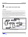
BASIC TIMER & WDT
BASIC TIMER & WATCHDOG TIMER
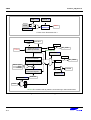
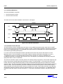
1. OVERVIEW
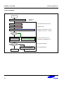
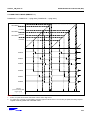
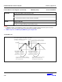
Basic Timer/Watch-Dog Timer can be used to resume the controller operation when it is disturbed due to noise,
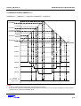
system error, or other kinds of malfunction.
To have a configuration on Watch-dog Timer, the overflow signal from 8-bit Basic Timer should be fed to the clock
input of 3-bit Watch-dog Timer as shown in below figure. User can enable or disable the Watch-dog Timer by
software, i.e., by controlling the configuration in BTCON register. If users do not want to use the configuration of
Watch-dog Timer, the 8-bit Basic Timer can only be used as a normal interval timer to request the interrupt service.
Also, it works to signal the end of the required oscillation interval after a reset or Stop mode release.
For example, the Basic Timer can give the overflow signal to necessary logic blocks after a reset or release from
Stop mode. In this case, the overflow signal from Basic Timer can guarantee the necessary time delay for stable
clock from external oscillator circuit.
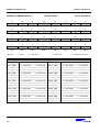
BTCON.0 : WDTC
BTCON.3-.2: CS
RESET or STOP or IDLE
BTCON.15-.8: WDTE
Clear
CLK DIV
Fin/212
Fin
4,6 or 8MHz
Fin/210
Fin/26
Fin/25
BTCNT.7-.0: BCV
8-Bit Basic Counter
BTCNT.11-.8: WCV
3-Bit WDTimer Counter
Clear
OVF
nRESET
INTMSK
INTPND
INT_BT
After releasing from RESET or STOP mode,
BTCON.1: BTC
RESET or STOP
when BTCNT.4 is set , CPU Start.
.
Figure 3-1. Basic Timer Block Diagram
NOTE: In the clock fail mode, the clock source of basic timer is internal oscillator.
3-1
BASIC TIMER & WDT
S3F401F_UM_REV1.00
2. FUNCTION DESCRIPTION
2.1 INTERVAL TIMER FUNCTION
The primary function of Basic Timer is to measure the elapsed time between events. The standard time interval is
equal to 256 basic timer clock pulses, which is an overflow signal from 8-bit Basic Timer.
The content of 8-bit counter register, BTCNT, is increased it content every when a clock signal is detected which
corresponds to the frequency selected by BTCON. The BTCNT continues its counting until an overflow occurs, i.e.,
the content reaches to 255. An overflow can cause the BT interrupt pending flag to be set, which signals that the
designated time interval has elapsed. In this case, when an interrupt request is generated, BTCNT is cleared to all
zero, and the counting continues from 0x00, again.
2.1.1 Oscillation Stabilization Using Interval Timer Function
You can use the Basic Timer to have programmable delay time, which is necessary for stabilizing the clock signal
from oscillator circuit after reset or Stop mode release.
When the S3F401F is in Stop mode, the reset or external interrupt request can wake up the S3F401F. Please
understand that the oscillator circuit is in disable state when the S3F401F is in Stop mode. In case of wake-up by
reset, the oscillator should start first. Because the default clock division ratio is Fin / 2^12, the Fin / 2^12 clock will be
fed to the 8-bit Basic Timer. When an overflow occurs from Bit 4 of BTCNT register(Not using 8-bit, but 4-bit of Basic
Timer), this kind of overflow signal can release the clock blocking to CPU. In other word, the normal clock can be fed
to S3F401F when an overflow of Bit 4 in Basic Timer. In case of wake-up by external interrupt request, the only
difference from reset, is clock division ratio. While we should use the default value of clock division ratio for the case
of wake-up by reset, we use the pre-defined value of clock division ratio before entering into Stop mode for the case
of wake-up by external interrupt request. In any case, the CPU can resume its operation when normal clock can be
fed to the blocks in S3F401F.
In summary, please take following sequence for releasing S3F401F from Stop mode:
1. When S3F401F is in Stop mode, the escape from Stop mode can be made by a power-on reset or an external
interrupt. At same time, the oscillator can start its oscillation.
2. In case of wake-up by power-on reset, the Basic Timer will increase its content(BTCNT) at the rate of Fin / 2^12,
which is the default rate of clock division ration. In case of wake-up by external interrupt request, the Basic Timer
will increase its content (BTCNT) at the rate of preset value, which is written before entering into Stop mode.
3. The normal clock from oscillator will be delayed to be fed to all logic blocks inside S3F401F until the 4th bit of
Basic Timer is generated. It means that you can use the Basic Timer to guarantee the stable clock from
oscillator, i.e., waiting up to stable oscillation.
4. When the normal clock can be fed to S3F401F, the S3F401F can resume the operation.
3-2
S3F401F_UM_REV1.00
BASIC TIMER & WDT
2.2 WATCHDOG TIMER OPERATION
The Basic Timer can also be used as a "Watch-Dog" Timer to recover the S3F401F from the unexpected program
sequence, that is, system or program operation error due to external factor. For example, the external noise can
cause this kind of situation, which means that the CPU is running the unexpected code sequence, i.e., malfunction
of CPU. To recover the CPU from the unexpected sequence, the Watch-Dog Timer should reset the CPU in case of
malfunction. But, during normal sequence, the instruction which clear the Watch-Dog Timer before the overflow of
Watch-Dog Timer (Within a given period) should be executed at the proper points in a program. If this instruction can
be executed in certain circumstance, it means the overflow of Watch-Dog Timer and it can generate the internal
reset signal generation to restart the CPU from the beginning. In summary, an operation of Watch-Dog Timer is as
follows:
•
Each time BTCNT overflows, an overflow signal should be sent to the Watch-Dog Timer Counter, WDTCNT.
•
If WDTCNT overflows, system reset should be generated.
NOTE
A reset signal can clear the BTCON as 0x0000. This value can enable the Watch-Dog Timer because it is
not 0xA5 (Please understand the Watch-Dog Timer can be disable when its content (WDTE field in
BTCON[15:8] register) is 0xA5). For normal program sequence, the application program should prevent the
overflow. To do this, the WDTCNT value should be cleared (by writing a "1" to WDTC bit of the Basic Timer
Control Register (BTCON[0])) before the overflow occurs.
3-3
BASIC TIMER & WDT
S3F401F_UM_REV1.00
2.3 TIMER DURATION
2.3.1 Basic Timer Duration
The Basic Timer Counter, BTCNT, can be used to specify the time-out duration, and is a free-running 8-bit counter.
Please keep below table as reference for duration of timer.
Clock Source
Interval Time
Fin = 4MHz
Fin / 2^5
8 us
2^5 * 2^8 / Fin = 2.048 ms
Fin = 4MHz
Fin / 2^6
16 us
2^6 * 2^8 / Fin = 4.098 ms
Fin = 4MHz
Fin / 2^10
256 us
2^10 * 2^8 / Fin = 65.536 ms
Fin = 4MHz
Fin / 2^12
1024 us
2^12 * 2^8 / Fin = 262.144 ms
Resolution
Interval Time
Clock Source
Fin = 6MHz
Fin / 2^5
5.33 us
2^5 * 2^8 / Fin = 1.364 ms
Fin = 6MHz
Fin / 2^6
10.66us
2^6 * 2^8 / Fin = 2.728 ms
Fin = 6MHz
Fin / 2^10
166.66 us
2^10 * 2^8 / Fin = 42.664 ms
Fin = 6MHz
Fin / 2^12
682.66 us
2^12 * 2^8 / Fin = 174.760 ms
Resolution
Interval Time
Clock Source
3-4
Resolution
Fin = 8MHz
Fin / 2^5
4 us
2^5 * 2^8 / Fin = 1.024 ms
Fin = 8MHz
Fin / 2^6
8 us
2^6 * 2^8 / Fin = 2.048 ms
Fin = 8MHz
Fin / 2^10
128 us
2^10 * 2^8 / Fin = 32.768 ms
Fin = 8MHz
Fin / 2^12
512 us
2^12 * 2^8 / Fin = 131.072 ms
S3F401F_UM_REV1.00
BASIC TIMER & WDT
2.4 WATCH DOG TIMER DURATION
The Watch-Dog Timer Counter, WTCNT, can be used to specify the time-out duration and is a free-running 3-bit
counter. To enable Watch-Dog Timer, you should write the data in BTCON[15:8] register except 0xA5. In case of
0xA5, it will disable the Watch-Dog Timer. After writing certain value in BTCON[15:8] except 0xA5, there will be a
system reset if the overflow occurs.
Clock Source
Resolution
Watch-Dog Timer Interval Time
Fin = 4MHz
Fin / 2^5* 2^8
2.048 ms
2^5 * 2^8 * 2^3 / Fin =16.384 ms
Fin = 4MHz
Fin / 2^6* 2^8
4.098 ms
2^6 * 2^8 * 2^3 / Fin = 32.784 ms
Fin = 4MHz
Fin / 2^10 * 2^8
65.536 ms
2^10 * 2^8 * 2^3 / Fin = 524.288 ms
Fin = 4MHz
Fin / 2^12 * 2^8
262.144 ms
2^12 * 2^8 *2^3 / Fin = 2.097 s
Resolution
Watch-Dog Timer Interval Time
Clock Source
Fin = 6MHz
Fin / 2^5* 2^8
1.364 ms
2^5 * 2^8 * 2^3 / Fin = 10.912 ms
Fin = 6MHz
Fin / 2^6* 2^8
2.728 ms
2^6 * 2^8 * 2^3 / Fin = 21.824 ms
Fin = 6MHz
Fin / 2^10 * 2^8
42.664 ms
2^10 * 2^8 * 2^3 / Fin = 341.312 ms
Fin = 6MHz
Fin / 2^12 * 2^8
174.760 ms
2^12 * 2^8 *2^3 / Fin = 1.398 s
Resolution
Watch-Dog Timer Interval Time
Clock Source
Fin = 8MHz
Fin / 2^5* 2^8
1.024 ms
2^5 * 2^8 * 2^3 / Fin = 8.192 ms
Fin = 8MHz
Fin / 2^6* 2^8
2.048 ms
2^6 * 2^8 * 2^3 / Fin = 16.384 ms
Fin = 8MHz
Fin / 2^10* 2^8
32.768 ms
2^10 * 2^8 * 2^3 / Fin = 262.144 ms
Fin = 8MHz
Fin / 2^12 * 2^8
131.072 ms
2^12 * 2^8 *2^3 / Fin = 1.048 s
3-5
BASIC TIMER & WDT
S3F401F_UM_REV1.00
3. REGISTERS DESCRIPTION
Base Address − 0xFF00_4000
Table 3-1. Basic timer & WDT Special Function Registers
Offset Address
3-6
Register
Description
0x000
BTCON
Basic timer control register
0x004
BTCNT
Basic timer count register
R/W
Reset Value
R/W
0x0000_0000
R
0x0000_0000
S3F401F_UM_REV1.00
BASIC TIMER & WDT
Basic Timer Control Register
BTCON (0x000)
Access: Read/Write
31
30
29
28
27
26
25
24
−
−
−
−
−
−
−
−
R/W-0
R/W-0
R/W-0
R/W-0
R/W-0
R/W-0
R/W-0
R/W-0
23
22
21
20
19
18
17
16
−
−
−
−
−
−
−
−
R/W-0
R/W-0
R/W-0
R/W-0
R/W-0
R/W-0
R/W-0
R/W-0
15
14
13
12
11
10
9
8
WDTE[15:8]
R/W-0
R/W-0
R/W-0
R/W-0
R/W-0
R/W-0
R/W-0
R/W-0
7
6
5
4
3
2
1
0
−
−
−
−
BTC
WDTC
R/W-0
R/W-0
R/W-0
R/W-0
R/W-0
R/W-0
W: Write
R: Read
-0: 0 After reset
WDTC
Watch-Dog Timer Clear Bit
CS[3:2]
R/W-0
R/W-0
-1: 1 After reset
-U: Undefined after reset
0 = No effect
1 = Watch-Dog Timer Counter will be cleared to all zero.
Note:
BTC
This bit is auto-clear bit.
Basic Timer Clear Bit
0 = No effect
1 = Basic Timer Counter will be cleared to all zero.
Note: This bit is auto-clear bit.
CS
Clock Source Select Field
00 = Fin / 2^12
01 = Fin / 2^10
10 = Fin / 2^6
11 = Fin / 2^5
WDTE
Watchdog Timer Enable Bit
0xA5 = Watchdog Timer Counter will be stopped
Others = Watchdog Timer Counter can enable, and make a system reset when overflow
DBGEN
Debug Enable Bit
0 = BT/WDT is halted during processor debug mode.
1 = BT/WDT is not halted during processor debug mode.
3-7
BASIC TIMER & WDT
S3F401F_UM_REV1.00
Basic Timer Count Register
BTCNT (0x004)
Access: Read Only
31
30
29
28
27
26
25
24
−
−
−
−
−
−
−
−
R-0
R-0
R-0
R-0
R-0
R-0
R-0
R-0
23
22
21
20
19
18
17
16
−
−
−
−
−
−
−
−
R-0
R-0
R-0
R-0
R-0
R-0
R-0
R-0
15
14
13
12
11
10
9
8
−
−
−
−
−
R-0
R-0
R-0
R-0
R-0
R-0
R-0
R-0
7
6
5
4
3
2
1
0
R-0
R-0
R-0
R-0
WCV[10:8]
BCV[7:0]
R-0
R-0
R-0
R-0
W: Write
R: Read
-0: 0 After reset
BCV
Basic Timer Count Value Field
0x00 ~ 0xFF
WCV
Watchdog Timer Count Value Field
0x0 ~ 0x7
3-8
-1: 1 After reset
-U: Undefined after reset
S3F401F_UM_REV1.00
4
ENCODER COUNTER
ENCODER COUNTER
1. OVERVIEW
The S3F401F has two encoder counter blocks. The encoder counter block can be used for measuring position and
speed.
The following list summarizes the main features of the encoder counter block:
•
Three input signals: PHASEA, PHASEB and PHASEZ
•
Two 16-bit up/down counters: PCNT, SCNT
•
Capture function supports for slow rotating: PACAP, PBCAP
•
Filter in the PHASEZ and edge selector of PHASEZ
4-1
ENCODER COUNTER
S3F401F_UM_REV1.00
ENCCON1.8:PACNTCL
ENCCON1.9: PAEN
ENCCON1.8:PACNTCL
Clear
Clear
INTMASK
4-bit
PACLK PACNT.15-.0:PACV
Prescaler
16-bit Up Counter
ENCCLK
INT_OVF_A
INTPND
INTMASK
Clear
INT_CAP_A
INTPND
PACAP.15-.0:PACAPDAT
ENCCON1.11-.10: ESELA
PA Capure Data Register
ENCCON1.0: PBCNTCL
ENCCON1.1: PBEN
ENCCON1.0: PBCNTCL
Clear
Clear
INTMASK
4-bit
PBCLK PBCNT.15-.0:PBCV
Prescaler
16-bit Up Counter
ENCCLK
INT_OVF_B
INTPND
INTMASK
Clear
INT_CAP_B
INTPND
ENCCON1.3-.2: ESELB
PBCAP.15-.0:PBCAPDAT
PB Capure Register
ENCCON0.7: PZCLEN
PHASEA
PHASEB
PHASEZ
Filter
Edge
selector
Clear
PCNT.15-.0: PCV
16-bit Up/Down
Position Counter
Clear
INTMASK
16-bit Comparator
ENCCON0.6-.4:ENCFILTER
ENCCON0.3:ESELZ
ENCCON0.0: PCNTCL
INTPND
PREF.15-.0:PREFDAT
16-bit Position Reference
SCNT.15-.0: SCV
16-bit Up/Down
Speed Counter
Clear
16-bit Comparator
SREF.15-.0:SREFDAT
16-bit Speed Reference
ENCCON0.1: SCNTCL
INTMASK
INTPND
INT_MAT_S
INTMASK
INTPND
Figure 4-1. Encoder Counter Block Diagram
4-2
INT_MAT_P
INT_PHASEZ
S3F401F_UM_REV1.00
ENCODER COUNTER
2. FUNCTION DESCRIPTION
PHASEA
PHASEB
PCNT
+1 +1 +1 +1 +1 +1 +1 +1 +1 +1 +1
ENCSTATUS.0 = DIRECTION
-1 -1 -1 -1 -1
0
1
Figure 4-2. Position Counter Operation
To measure position and speed the encoder counter has the three input signals, PHASEA, PHASEB and PHASEZ.
The difference of phase between phase A and phase B pulse is 90°. The input of PHASEZ is one-pulse signal to be
generated at specific position 1 cyclic.
2.1 POSITION COUNTER OPERATION
Direction of Rotation
When DIRECTIONT bit is ‘0’, the counter value of PCNT increases. On the other hands, when DIRECTION bit is ‘1’,
PCNT decreases. Position counter is an up and down counter. The DIRECTION bit status and counting direction are
decided which phase signal between PHASE A and PHASE B is leading.
NOTE
Although the PBEN and PAEN bit are ‘0’, disable, if inserted any signal into PHASE A, PHASE B input port
and CAP_A0/A1 and CAP_B0/B1 interrupt are unmask, those interrupts occur until interrupts mask or
non-signal.
4-3
ENCODER COUNTER
S3F401F_UM_REV1.00
3. REGISTERS DESCRIPTION
Base Address − ENC0: 0xFF02_8000
− ENC1: 0xFF02_C000
Table 4-1. ENC Special Function Registers
Offset Address
Register
Description
R/W
Reset value
0x000
ENCCON0
Encoder counter control register 0
R/W
0x0000_0000
0x004
ENCCON1
Encoder counter control register 1
R/W
0x0000_0000
0x008
ENCSTATUS
Encoder counter status register
R/W
0x0000_0000
0x00C
PCNT
16bit Position counter register
R/W
0x0000_0000
0x010
PREF
16bit Position reference register
R/W
0x0000_0000
0x014
SCNT
16bit Speed counter register
R/W
0x0000_0000
0x018
SREF
16bit Speed reference register
R/W
0x0000_0000
0x01C
PACNT
16bit Phase A capture counter register
R/W
0x0000_0000
0x020
PACAP
16bit Phase A capture data register
R/W
0x0000_0000
0x024
PBCNT
16bit Phase B capture counter register
R/W
0x0000_0000
0x028
PBCAP
16bit Phase B capture data register
R/W
0x0000_0000
NOTE: The PCNT, SCNT are 2’s complement. The range of PCNT and SCNT are -215 ~ (+215-1).
4-4
S3F401F_UM_REV1.00
ENCODER COUNTER
Encoder Counter Control Register 0
ENCCON0 (0x000)
Access: Read/Write
31
30
29
28
27
26
25
24
−
−
−
−
−
−
−
−
R/W-0
R/W-0
R/W-0
R/W-0
R/W-0
R/W-0
R/W-0
R/W-0
23
22
21
20
19
18
17
16
−
−
−
−
−
−
−
−
R/W-0
R/W-0
R/W-0
R/W-0
R/W-0
R/W-0
R/W-0
R/W-0
15
14
13
12
11
10
9
8
−
−
−
−
DBGEN
R/W-0
R/W-0
R/W-0
R/W-0
R/W-0
R/W-0
R/W-0
R/W-0
7
6
5
4
3
2
1
0
ESELZ
ENCEN
SCNTCL
PCNTCL
R/W-0
R/W-0
R/W-0
R/W-0
PZCLEN
R/W-0
ENCFILTER[6:4]
R/W-0
R/W-0
R/W-0
W: Write
R: Read
-0: 0 After reset
PCNTCL
Position Counter (PCNT) Clear Bit
ENCCLKSEL[10:8]
-1: 1 After reset
-U: Undefined after reset
0 = No effect
1 = Clear the counter register
Note: This bit is auto-clear bit.
SCNTCL
Speed Counter (SCNT) Clear Bit
0 = No effect
1 = Clear the counter register
Note: This bit is auto-clear bit.
ENCEN
Encoder Counter Block Enable Bit
0 = Disable encoder counter block
1 = Enable encoder counter block
ESELZ
Phase Z Edge Type Selection Field
0 = Falling edge is selected for PHASEZ
1 = Rising edge is selected for PHASEZ
ENCFILTER
Filter Clock Selection Field of Encoder Counter
000 = ENCCLK
100 = ENCCLK /16
001 = ENCCLK /2
101 = ENCCLK /32
010 = ENCCLK /4
110 = ENCCLK /64
011 = ENCCLK /8
111 = ENCCLK /128
Note: Only 5 times same level in a row is recognized as effective signal.
4-5
ENCODER COUNTER
Encoder Counter Control Register 0 (Continued)
PZCLEN
S3F401F_UM_REV1.00
ENCCON0 (0x000)
Access: Read/Write
PCNT Clear Enable by Phase Z.
0 = Enable
1 = Disable
ENCCLKSEL
DBGEN
Encoder Counter Clock (DECCLK) Selection Field
000 = ENCCLK
100 = ENCCLK /16
001 = ENCCLK /2
101 = ENCCLK /32
010 = ENCCLK /4
110 = ENCCLK /64
011 = ENCCLK /8
111 = ENCCLK /128
Debug Enable Bit
0 = ENC is halted during processor debug mode.
1 = ENC is not halted during processor debug mode. Although you break the debugger, you
can see count register and several bits of status register changing according to the operation
setting.
NOTE
4-6
Several bits of status - These bits are ENCSTATUS.0, ENCSTATUS.2 and ENCSTATUS.3. Because
these bits can a read-only bit.
S3F401F_UM_REV1.00
ENCODER COUNTER
Encoder Counter Status Register
ENCSTATUS (0x008)
Access: Read/Write
31
30
29
28
27
26
25
24
−
−
−
−
−
−
−
−
R/W-0
R/W-0
R/W-0
R/W-0
R/W-0
R/W-0
R/W-0
R/W-0
23
22
21
20
19
18
17
16
−
−
−
−
−
−
−
−
R/W-0
R/W-0
R/W-0
R/W-0
R/W-0
R/W-0
R/W-0
R/W-0
15
14
13
12
11
10
9
8
PAEN
PACNTCL
PRESCALEA[15:12]
ESELA[11:10]
R/W-0
R/W-0
R/W-0
R/W-0
R/W-0
R/W-0
R/W-0
R/W-0
7
6
5
4
3
2
1
0
−
−
−
−
PASTAT
PBSTAT
GLITCH
DIRECTION
R/W-0
R/W-0
R/W-0
R/W-0
R/W-0
R/W-0
R/W-0
R/W-0
W: Write
R: Read
-0: 0 After reset
DIRECTION
Direction of Motor Rotation Bit
-1: 1 After reset
-U: Undefined after reset
0 = Clockwise - The value of PCNT is increased.
1 = Counter-clockwise - The value of PCNT is decreased.
Note: This bit is read-only bit.
GLITCH
Glitch Detection Field of Phase A, Phase B and Phase Z
READ
0 = Glitch is not occurred
1 = Glitch is occurred
WRITE
0 = Glitch bit is cleared
1 = No effect
Note: Glitch is detected according to the checking whether if 5 times same level in a row is recognized as
effective signal.
PBSTAT
Phase B Status Bit
0 = Low level
1 = High level
Note: This bit is read only bit.
PASTAT
Phase A Status Bit
0 = Low level
1 = High level
Note:
This bit is read only bit.
4-7
ENCODER COUNTER
S3F401F_UM_REV1.00
Encoder Counter Status Register (Continued)
OFPCNT
ENCSTATUS (0x008)
Access: Read/Write
Overflow Detection of PCNT
READ
0 = Overflow is not occurred
1 = Overflow is occurred
WRITE
0 = OFPCNT bit is cleared.
1 = No effect
UFPCNT
Underflow Detection of PCNT
READ
0 = Underflow is not occurred
1 = Underflow is occurred
WRITE
0 = UFPCNT bit is cleared.
1 = No effect
OFSCNT
Overflow Detection of SCNT
READ
0 = Overflow is not occurred
1 = Overflow is occurred
WRITE
0 = OFSCNT bit is cleared.
1 = No effect
UFSCNT
Underflow Detection of SCNT
READ
0 = Underflow is not occurred
1 = Underflow is occurred
WRITE
0 = UFSCNT bit is cleared.
1 = No effect
NOTE
4-8
ENCSTATUS.4− .7 are cleared automatically by counter clear signal. (PHASEZ, ENCCON0.1− .0)
S3F401F_UM_REV1.00
ENCODER COUNTER
16 Bit Position Counter Register
PCNT (0x00C)
Access: Read/Write
31
30
29
28
27
26
25
24
−
−
−
−
−
−
−
−
R/W-0
R/W-0
R/W-0
R/W-0
R/W-0
R/W-0
R/W-0
R/W-0
23
22
21
20
19
18
17
16
−
−
−
−
−
−
−
−
R/W-0
R/W-0
R/W-0
R/W-0
R/W-0
R/W-0
R/W-0
R/W-0
15
14
13
12
11
10
9
8
PCV[15:8]
R/W-0
R/W-0
R/W-0
R/W-0
R/W-0
R/W-0
R/W-0
R/W-0
7
6
5
4
3
2
1
0
R/W-0
R/W-0
R/W-0
R/W-0
PCV[7:0]
R/W-0
R/W-0
R/W-0
R/W-0
W: Write
R: Read
-0: 0 After reset
-1: 1 After reset
PCV
The Current Position Counter Value Field
-U: Undefined after reset
0x0000 ~ 0xFFFF
16 Bit Position Reference Register
PREF (0x010)
Access: Read/Write
31
30
29
28
27
26
25
24
−
−
−
−
−
−
−
−
R/W-0
R/W-0
R/W-0
R/W-0
R/W-0
R/W-0
R/W-0
R/W-0
23
22
21
20
19
18
17
16
−
−
−
−
−
−
−
−
R/W-0
R/W-0
R/W-0
R/W-0
R/W-0
R/W-0
R/W-0
R/W-0
15
14
13
12
11
10
9
8
PREFDAT [15:8]
R/W-0
R/W-0
R/W-0
R/W-0
R/W-0
R/W-0
R/W-0
R/W-0
7
6
5
4
3
2
1
0
R/W-0
R/W-0
R/W-0
R/W-0
PREFDAT [7:0]
R/W-0
R/W-0
R/W-0
-0: 0 After reset
R/W-0
W: Write
R: Read
-1: 1 After reset
PREFDAT
The Reference Value for Position Counter
-U: Undefined after reset
0x0000 ~ 0xFFFF
4-9
ENCODER COUNTER
S3F401F_UM_REV1.00
16 Bit Speed Counter Register
SCNT (0x014)
Access: Read/Write
31
30
29
28
27
26
25
24
−
−
−
−
−
−
−
−
R/W-0
R/W-0
R/W-0
R/W-0
R/W-0
R/W-0
R/W-0
R/W-0
23
22
21
20
19
18
17
16
−
−
−
−
−
−
−
−
R/W-0
R/W-0
R/W-0
R/W-0
R/W-0
R/W-0
R/W-0
R/W-0
15
14
13
12
11
10
9
8
SCV [15:8]
R/W-0
R/W-0
R/W-0
R/W-0
R/W-0
R/W-0
R/W-0
R/W-0
7
6
5
4
3
2
1
0
R/W-0
R/W-0
R/W-0
R/W-0
SCV [7:0]
R/W-0
R/W-0
R/W-0
R/W-0
W: Write
R: Read
-0: 0 After reset
-1: 1 After reset
SCV
The Current Speed Counter Value Field
-U: Undefined after reset
0x0000 ~ 0xFFFF
16 Bit Speed Reference Register
SREF (0x018)
Access: Read/Write
31
30
29
28
27
26
25
24
−
−
−
−
−
−
−
−
R/W-0
R/W-0
R/W-0
R/W-0
R/W-0
R/W-0
R/W-0
R/W-0
23
22
21
20
19
18
17
16
−
−
−
−
−
−
−
−
R/W-0
R/W-0
R/W-0
R/W-0
R/W-0
R/W-0
R/W-0
R/W-0
15
14
13
12
11
10
9
8
SREFDAT [15:8]
R/W-0
R/W-0
R/W-0
R/W-0
R/W-0
R/W-0
R/W-0
R/W-0
7
6
5
4
3
2
1
0
R/W-0
R/W-0
R/W-0
R/W-0
SREFDAT [7:0]
R/W-0
R/W-0
R/W-0
-0: 0 After reset
R/W-0
W: Write
R: Read
SREFDAT
The Reference Value for Speed Counter
0x0000 ~ 0xFFFF
4-10
-1: 1 After reset
-U: Undefined after reset
S3F401F_UM_REV1.00
ENCODER COUNTER
16 Bit Phase A Capture Counter Register
PACNT (0x01C)
Access: Read/Write
31
30
29
28
27
26
25
24
−
−
−
−
−
−
−
−
R/W-0
R/W-0
R/W-0
R/W-0
R/W-0
R/W-0
R/W-0
R/W-0
23
22
21
20
19
18
17
16
−
−
−
−
−
−
−
−
R/W-0
R/W-0
R/W-0
R/W-0
R/W-0
R/W-0
R/W-0
R/W-0
15
14
13
12
11
10
9
8
PACV [15:8]
R/W-0
R/W-0
R/W-0
R/W-0
R/W-0
R/W-0
R/W-0
R/W-0
7
6
5
4
3
2
1
0
R/W-0
R/W-0
R/W-0
R/W-0
PACV [7:0]
R/W-0
R/W-0
R/W-0
R/W-0
W: Write
R: Read
-0: 0 After reset
-1: 1 After reset
PACV
The Phase A Capture Counter Value Field
-U: Undefined after reset
0x0000 ~ 0xFFFF
16 Bit Phase A Capture Data Register
PACAP (0x020)
Access: Read/Write
31
30
29
28
27
26
25
24
−
−
−
−
−
−
−
−
R/W-0
R/W-0
R/W-0
R/W-0
R/W-0
R/W-0
R/W-0
R/W-0
23
22
21
20
19
18
17
16
−
−
−
−
−
−
−
−
R/W-0
R/W-0
R/W-0
R/W-0
R/W-0
R/W-0
R/W-0
R/W-0
15
14
13
12
11
10
9
8
PACAPDAT [15:8]
R/W-0
R/W-0
R/W-0
R/W-0
R/W-0
R/W-0
R/W-0
R/W-0
7
6
5
4
3
2
1
0
R/W-0
R/W-0
R/W-0
R/W-0
PACAPDAT [7:0]
R/W-0
R/W-0
R/W-0
R/W-0
W: Write
R: Read
-0: 0 After reset
PACAPDAT
The Phase A Captured Value Field
-1: 1 After reset
-U: Undefined after reset
0x0000 ~ 0xFFFF
4-11
ENCODER COUNTER
S3F401F_UM_REV1.00
16 Bit t Phase B Capture Counter Register
PBCNT (0x024)
Access: Read/Write
31
30
29
28
27
26
25
24
−
−
−
−
−
−
−
−
R/W-0
R/W-0
R/W-0
R/W-0
R/W-0
R/W-0
R/W-0
R/W-0
23
22
21
20
19
18
17
16
−
−
−
−
−
−
−
−
R/W-0
R/W-0
R/W-0
R/W-0
R/W-0
R/W-0
R/W-0
R/W-0
15
14
13
12
11
10
9
8
PBCV [15:8]
R/W-0
R/W-0
R/W-0
R/W-0
R/W-0
R/W-0
R/W-0
R/W-0
7
6
5
4
3
2
1
0
R/W-0
R/W-0
R/W-0
R/W-0
PBCV [7:0]
R/W-0
R/W-0
R/W-0
R/W-0
W: Write
R: Read
-0: 0 After reset
-1: 1 After reset
PBCV
The Phase B Capture Counter Value Field
-U: Undefined after reset
0x0000 ~ 0xFFFF
16 Bit Phase B Capture Data Register
PBCAP (0x028)
Access: Read/Write
31
30
29
28
27
26
25
24
−
−
−
−
−
−
−
−
R/W-0
R/W-0
R/W-0
R/W-0
R/W-0
R/W-0
R/W-0
R/W-0
23
22
21
20
19
18
17
16
−
−
−
−
−
−
−
−
R/W-0
R/W-0
R/W-0
R/W-0
R/W-0
R/W-0
R/W-0
R/W-0
15
14
13
12
11
10
9
8
PBCAPDAT [15:8]
R/W-0
R/W-0
R/W-0
R/W-0
R/W-0
R/W-0
R/W-0
R/W-0
7
6
5
4
3
2
1
0
R/W-0
R/W-0
R/W-0
R/W-0
PBCAPDAT [7:0]
R/W-0
R/W-0
R/W-0
R/W-0
W: Write
R: Read
-0: 0 After reset
PBCAPDAT
The Phase B Captured Value Field
0x0000 ~ 0xFFFF
4-12
-1: 1 After reset
-U: Undefined after reset
S3F401F_UM_REV1.00
5
INTERNAL FLASH ROM
INTERNAL FLASH ROM
1. OVERVIEW
The S3F401F has an on-chip flash ROM, internally. The memory flash size is 256Kbytes. To improve operating
speed, the memory is composed of two interleaved flash memories.
1.2 FEATURES
•
Flash memory size: 256Kbytes
•
Two working modes: Non-interleave mode, Interleave mode
•
Two programming modes: User program mode, Tool program mode
•
Protection supports: Hardware protection, Read protection
2. BLOCK DIAGRAM
Figure 5-1. Flash Memory Controller Read/Write Block Diagram
5-1
INTERNAL FLASH ROM
S3F401F_UM_REV1.00
3. FLASH CONFIGURATION
3.1 FLASH ROM CONFIGURATION
The 256KBytes Flash ROM consists of 256 sectors. Each sector consists of 1024bytes. So, the total size of flash
ROM is 256(sector number) x 1024(each sector size) bytes (256Kbyte). You can erase the flash memory a
sector-unit at a time and write the data into the flash memory a word-unit at a time.
3.2 ADDRESS ALIGNMENT
To set an address value in FMADDR register, abide by the following rules.
♦
Sector Erase
When erasing a sector, the lower 10-bits of address should be ‘0’, because the size of a sector is 1024Bytes.
You can select one as the SECTOR_ORDER from 0 to 255, among 256 sectors.
− FMADDR [31:0] = (SECTOR_ ORDER << 10)
♦
Program
When programming Flash ROM, the lower 2-bits should be ‘0’, because data should be written to the Flash
ROM by a word-unit (4bytes). You can select one as the ADDRESS from 0x0000 to 0x3FFFF, in 256Kbytes
range. In the tool program mode, the low 2-bit address also should be 00b.
− FMADDR [31:0] = ADDRESS & 0xFFFFFFFC
3.3 WORKING MODE
There are two-different working modes following:
♦
NON-INTERLEAVE MODE
The flash memories are able to work at the system clock frequency (MCLK). In this case, all read accesses are
executed with no wait state.
♦
INTERLEAVE MODE
The flash memories work at the system clock frequency (MCLK) divided by 2. In this case, non-sequential read
accesses require one wait state and sequential read accesses are executed with no wait state. Thanks to a
cache buffer, fetch accesses at consecutive address are performed with no wait state.
3.4 PROGRAM MODE
For writing the data in flash ROM, you can access the flash ROM by a program or the external serial interface.
Because of the feature of NOR flash memory, you can program the data in any address and in any time. The size of
embedded flash memory in S3F401F is 256K-byte and it has the following features:
♦
User program mode (AHB Interface)
♦
Tool program mode (Use the dedicated serial interface)
♦
Protection mode: hardware protection and read protection
The S3F401F has several pins used for flash ROM writer to read/write/erase the flash memory (VDDIO[3:0],
VSSIO[3:0], nRESET, VDDCORE[3:0], VSSCORE[3:0], SDAT, SCLK), which is the programming by tool program
mode. These several pins are multiplexed with other functional pins.
5-2
S3F401F_UM_REV1.00
INTERNAL FLASH ROM
4. PROGRAMMING MODES
The Flash Memory Controller supports two kinds of program mode:
♦
User program mode
♦
Tool program mode
4.1 USER PROGRAM MODE
The user program mode for flash memory programming and sector erasing uses the internal high voltage generator,
which is necessary for flash memory programming and sector erasing. In other words, the Flash Memory Controller
has an internal high voltage pumping circuit. Therefore, high voltage to VPP pin is not needed. To program the data
into the flash ROM or sector erase in this mode, several control registers should be used, which will be explained
below.
4.1.1 The Program Procedure in the User Program Mode
In order to program to flash memory, you should write the address to be written into the address register (FMADDR)
and the data into the data register (FMDATA), respectively. As a next step, you should write the value 0x5A5A5A5A
into the FMKEY register. Before command bit set and start, you must enable flash counter clock
(FMUCON.7-UOSCEN bit Set). Finally, by writing the appropriate data into flash memory control register
(FMUCON). After the completion of the write operation, all registers except FMUCON.8bit (INTERLEAVE) will be
cleared. To perform the next writing operation, all register should be written again as before.
In order to perform sector erase procedure is the same as program procedure except not setting the data register
(FMDATA) in Flash Memory Controller.
In order to perform chip erase procedure will be enough to setting the key register (FMKEY) and control register
(FMUCON) in Flash Memory Controller.
5-3
INTERNAL FLASH ROM
S3F401F_UM_REV1.00
4.2 NORMAL PROGRAM
START
FMADDR 32-bit Address
FMDATA 32-bit Data
; Address set
; Data set
0x5A5A5A5A
FMKEY
; Key value set whenenver starts
FMUCON + UOSCEN Bit
; Enable flash osc
FMUCON + CommandBit + CPUStatus Bit + Start Bit
; Program command select & start
Command: FMUCON.2-UPGMR
CPUHOLD?
No
Yes
32-bit Data Writing
Command Bit Clear
COUNT=END?
Yes
+
Can be executed another
instruction in SRAM/SDRAM
; Check command bit to know
if operation is completed or not
; Compare End address
No
FMADDR New 32-bit Address
FMDATA New 32-bit Data
; Next address/data set
FINISH
Figure 5-2. Normal Program Flowchart
5-4
S3F401F_UM_REV1.00
INTERNAL FLASH ROM
4.3 OPTION PROGRAM
START
FMADDR 0x00000E38 or 0x00000E3C
FMDATA Option Bit Set
; Protection/Smart option register address set
; Option Bit set
0x5A5A5A5A
FMKEY
; Key value set whenenver starts
FMUCON + UOSCEN Bit
; Enable flash osc
FMUCON + CommandBit + CPUStatus Bit + Start Bit
; Program command select & start
Command: FMUCON.5-UOPGMR
CPUHOLD?
No
Yes
32-bit Data Writing
Command Bit Clear
COUNT=END?
+
Another instruction can be
executed in SRAM/SDRAM
; Check command bit to know
if operation is completed or not
; Compare End address
No
Yes
FMADDR 0x00000E38 or 0x00000E3C
FMDATA Other Option Bit Set
FINISH
Figure 5-3. Option Program Flowchart
5-5
INTERNAL FLASH ROM
S3F401F_UM_REV1.00
4.4 SECTOR ERASE
START
FMADDR Sector Base Address
FMKEY
; Address set
; Data set
0x5A5A5A5A
; Key value set whenenver starts
FMUCON + UOSCEN Bit
; Enable flash osc
FMUCON + CommandBit + CPUStatus Bit + Start Bit
; Program command select & start
Command: FMUCON.1 - USERSR
CPUHOLD?
No
Yes
32-bit Data Writing
Command Bit Clear
COUNT=END?
Another instruction can be
+ executed in SRAM/SDRAM
; Check command bit to know
if operation is completed or not
No
; Compare End address
FMADDR New 32-bit Address
FMDATA New 32-bit Data
; Next address/data set
Yes
FINISH
Figure 5-4. Sector Erase Flowchart
5-6
S3F401F_UM_REV1.00
INTERNAL FLASH ROM
4.5 CHIP ERASE FLOWCHART
START
FMKEY
0x5A5A5A5A
; Key value set whenenver starts
FMUCON + UOSCEN Bit
; Enable flash osc
FMUCON + CommandBit + CPUStatus Bit + Start Bit
; Program command select & start
Command: FMUCON.0 - UCERSR
CPUHOLD?
No
Yes
32-bit Data Writing
Command Bit Clear
Another instruction can be
+ executed in SRAM/SDRAM
; Check command bit to know
if operation is completed or not
FINISH
Figure 5-5. Chip Erase Flowchart
5-7
INTERNAL FLASH ROM
S3F401F_UM_REV1.00
4.6 TOOL PROGRAM MODE
The tool program mode is the flash memory program mode, which uses an equipment tool such as SPW2Plus Flash
ROM Writer or US-PRO Flash ROM Writer. If you want to make a dedicated Flash ROM writer for S3F401F, please
contact us for more detail document.
Table 5-1. The Pins Used to Read/Write/Erase the Flash ROM in Tool Program Mode
Pin No.
Pin Name
47
P1.15/SSPCLK0/INT15
SDAT
I/O
48
P1.16/SSPFSS0/INT16
SCLK
I
100
nRESET
RESET
I
Function
Serial bi-directional DATA pin(Output
when reading, Input when writing). Input &
push-pull output port can be assigned
Serial CLOCK input pin.
(Write speed: Max 200 KHz, Read speed :
Max 10 MHz)
Chip Initialization
VDD
P
3.3V Power supply pin for Flash block
16, 42, 66
VDDCORE[3:0]
32, 44, 93
VDDIO[3:0]
15, 41, 67
VSSCORE[3:0]
31, 43, 92
VSSIO[3:0]
Interface Signal
I/O
3.3V Power supply pin for I/O interface
VSS
P
GND Power supply pin for Flash block
GND Power supply pin for I/O interface
NOTE: More detail information about SPW2Plus and US-PRO is available in www.cnatech.com and www.seminix.com.
5-8
S3F401F_UM_REV1.00
INTERNAL FLASH ROM
5. DATA PROTECTION
The data programmed in flash memory need to be protected. For this situation, the Internal Flash Memory Controller
of S3F401F supports three kinds of protection mechanism.
♦
HARDWARE PROTECTION
Flash Full Region Protection or Selected Block Protection among total 16blocks
♦
READ PROTECTION
In the case of serial interface, Flash Read protection
♦
JTAG PROTECTION
These protection modes can be enabled by programming the protection option bits. The protection option bits can
be enabled or disabled with configuration at address 0x00000E38 and address 0x00000E3C.
5.1 PROTECTION OPTION CONFIGURATION
Table 5-2. Protection Option Address and Protection Bits
FMADDR
0x00000E3C
FMDATA
Description
Bit[7:0]
Not used
Bit[8]
0 : JTAG Protection Enable
Initial Value (at Fabrication)
Undefined
1
1 : JTAG Protection Disable
Bit[16:9]
Not used
Undefined
Bit[17]
0 : Hardware Protection Enable
1(Note 1)
1 : Hardware Protection Disable
Bit[26:18]
Not used
Bit[27]
0 : Serial Read Protection Enable
Undefined
1
1 : Serial Read Protection Disable
Bit[31:28]
Not used
Undefined
NOTE: For enabling Hardware Protection, you must set the Protection Option and Smart Option. That is, Protection Option is
used for enabling the Hardware Protection of selected group of sectors by Smart Option. Smart Option is used for
selecting the group of sectors for hardware protection. When you set the Smart Option, Hardware Protection bit in
Protection Option must be disabled. After you set the Smart Option, you should enable the hardware protection bit in
Protection Option.
5-9
INTERNAL FLASH ROM
S3F401F_UM_REV1.00
5.2 JTAG INTERFACE PROTECTION BIT 8
This Bit is used for JTAG Access enable or disable (If chip designers would like to debug through JTAG in initial chip
development state, JTAG Interface Protection Bit should be disabled, but, In final design development state, If chip
designers enable the JTAG interface Protection, other user can not access the flash memory data via JTAG
interface)
5.3 HARDWARE PROTECTION BIT 17
If Hardware Protection was enabled, user cannot write or erase the data in a flash memory area. In addition
Protection Option and Smart Option cannot be set or released. Hardware Protection function affects a tool program
mode as well as a user program mode. This protection can be released only by the chip erase execution.
Hardware Protection can be set in user program mode as follows. You should write 0x0E3C into the address and the
proper data (Refer to the above Protection Bit table) into the data register (FMDATA), respectively. As a next step,
you should write the values (0x5A5A5A5A) into key register(FMKEY). Finally, set FMUCON. Please refer to
figure3(Option Program Flowchart).
For enable to Hardware Protection, two Option registers, Protection Option(FMADDR: 0x0E3C) and Smart
Option(FMADDR: 0x0E38) are used. That is, Protection Option is used for enabling the hardware protection of the
selected group of sectors by Smart Option. Smart Option is used for selecting the group of sectors for hardware
protection. When you set the Smart Option, hardware protection bit in Protection Option must be disabled. After you
set the Smart Option, you should enable the hardware protection bit in Protection Option(FMADDR: 0x0E3C) On the
other way, you can set Hardware Protection in tool program mode by executing its functions and release Hardware
Protection by chip erase, which results in initializing all Protection bits, smart option bits and erasing internal Flash
ROM data,
5.3.1 SMART OPTION FMADDR - 0X0E38
In the Hardware protection function, the protection on certain block can be disabled by setting the corresponding
smart option bits. Four bits are allocated in the address of smart option (0x0E38) for this function.
To enable the protection function on a certain block,
> Configure the smart option bits in advance
> Configure the Hardware Protection Option (0x0E3C).
Table 5-3. Smart Option Address Configuration
FMADDR
FMDATA
Description
Reset Value
0x00000E38
Bit [15:0]
H/W protection is disable / enable : These bits are each mapped
to a corresponding group which is composed of 32 sectors(32KB). In
other word, the Bit[0] is mapped from sector 1 to sector 16. And the
Bit[1] is mapped from sector 17 to sector 32 and so on.
0xFFFF
Therefore, these 16 bits are used for 256KB internal Flash.
0 = Enable H/W protection of selected group
1 = Disable H/W protection of selected group
5-10
S3F401F_UM_REV1.00
INTERNAL FLASH ROM
Table 5-4. Hardware Protection Area
FMDATA[15:0]
Hardware Protection Area Sector
Protected Area Address
0xFFFE
Sector 000 ~ Sector 015
0x0000_0000 ~ 0x0000_3FFF
0xFFFD
Sector 016~ Sector 031
0x0000_4000 ~ 0x0000_7FFF
0xFFFB
Sector 032~ Sector 047
0x0000_8000 ~ 0x0000_BFFF
0xFFF7
Sector 048~ Sector 063
0x0000_C000 ~ 0x0000_FFFF
0xFFEF
Sector 064~ Sector 079
0x0001_0000 ~ 0x0001_3FFF
0xFFDF
Sector 080~ Sector 095
0x0001_4000 ~ 0x0001_7FFF
0xFFBF
Sector 096~ Sector 111
0x0001_8000 ~ 0x0001_BFFF
0xFF7F
Sector 112~ Sector 127
0x0001_C000 ~ 0x0001_FFFF
0xFEFF
Sector 128~ Sector 143
0x0002_0000 ~ 0x0002_3FFF
0xFDFF
Sector 144~ Sector 159
0x0002_4000 ~ 0x0002_7FFF
0xFBFF
Sector 160~ Sector 175
0x0002_8000 ~ 0x0002_BFFF
0xF7FF
Sector 176~ Sector 191
0x0002_C000 ~ 0x0002_FFFF
0xEFFF
Sector 192~ Sector 207
0x0003_0000 ~ 0x0003_3FFF
0xDFFF
Sector 208~ Sector 223
0x0003_4000 ~ 0x0003_7FFF
0xBFFF
Sector 224~ Sector 239
0x0003_8000 ~ 0x0003_BFFF
0x7FFF
Sector 240~ Sector 255
0x0003_C000 ~ 0x0003_FFFF
5.4 READ PROTECTION BIT 27
Most users want that their data and code in memory would not be read by others. Read Protection can give the
solution for it by preventing the flash data from being read serially in the tool program mode.
When this function is enabled, reading the flash data in the tool program mode will result in all zero read-out. You
should write the proper data (refer to the above Protection Bit table) into the address 0x00000E3C. The address
0x00000E3C should be written the register FMADDR. The data consisting of protection bit should be written the
register FMDATA. As a next step, you should write the values (0x5A5A5A5A) into key register (FMKEY). Finally, set
FMUCON. Please refer to figure3. (Option Sector Program Flowchart)
5-11
INTERNAL FLASH ROM
S3F401F_UM_REV1.00
6. REGISTERS DESCRIPTION
Base Address − 0xFFF0_0000
Table 5-5. Internal Flash Special Function Registers
Offset Address Register
Description
R/W
Reset Value
W
0x0000_0000
0x000
FMKEY
Flash program / erase Key register
0x004
FMADDR
Flash program / sector erase address register
R/W
0x0000_0000
0x008
FMDATA
Flash program data register
R/W
0x0000_0000
0x00C
FMUCON
Flash program/sector erase control register
R/W
0x0000_0000
0x010
FSO
Smart Option bits read register
R
0xXXXX
_FFFF
(PROT[15:0])
0x014
FPO
Protection Option bits read register
R
0bXXXX_1XXX_
(bit27:RDP)
XXXX_XX1X_
(bit17:HDP)
XXXX_XXX1_
(bit8:LDCP)
XXXX_ XXXX
5-12
S3F401F_UM_REV1.00
INTERNAL FLASH ROM
Flash Memory Key Register
31
30
FMKEY (0x000)
29
28
27
Access: Write Only
26
25
24
FMKEYDAT [31:24]
R/W-0
R/W-0
R/W-0
R/W-0
R/W-0
R/W-0
R/W-0
R/W-0
23
22
21
20
19
18
17
16
FMKEYDAT [23:16]
R/W-0
R/W-0
R/W-0
R/W-0
R/W-0
R/W-0
R/W-0
R/W-0
15
14
13
12
11
10
9
8
FMKEYDAT [15:8]
R/W-0
R/W-0
R/W-0
R/W-0
R/W-0
R/W-0
R/W-0
R/W-0
7
6
5
4
3
2
1
0
R/W-0
R/W-0
R/W-0
R/W-0
FMKEYDAT [7:0]
R/W-0
R/W-0
R/W-0
W: Write
R: Read
-0: 0 After reset
FMKEYDAT
Flash Memory Key
R/W-0
-1: 1 After reset
-U: Undefined after reset
Key register data to do program, erase, protection operation
To program any data into the flash memory by the user program mode, a specific key register
with 0x5A5A5A5A is required to prevent flash data from being destroyed under undesired
situations.
NOTE
The FMKEY register will be cleared automatically just after the completion of erase or program.
5-13
INTERNAL FLASH ROM
S3F401F_UM_REV1.00
Flash Memory Address Register
31
30
FMADDR (0x004)
29
28
27
Access: Read/Write
26
25
24
FMADDRDAT [31:24]
R/W-0
R/W-0
R/W-0
R/W-0
R/W-0
R/W-0
R/W-0
R/W-0
23
22
21
20
19
18
17
16
FMADDRDAT [23:16]
R/W-0
R/W-0
R/W-0
R/W-0
R/W-0
R/W-0
R/W-0
R/W-0
15
14
13
12
11
10
9
8
FMADDRDAT [15:8]
R/W-0
R/W-0
R/W-0
R/W-0
R/W-0
R/W-0
R/W-0
R/W-0
7
6
5
4
3
2
1
0
R/W-0
R/W-0
R/W-0
FMADDRDAT [7:0]
R/W-0
R/W-0
R/W-0
W: Write
R: Read
-0: 0 After reset
FMADDRDAT
Flash Memory Address
R/W-0
R/W-0
-1: 1 After reset
-U: Undefined after reset
Flash program / sector erase address register data
NOTE
In option programming, set FMADDR to 0x0E38 (Smart Option = Real Address “E”) or 0xE3C
(Protection Option = Real Address “F”) and FMDATA by the appropriate value and start the write
operation.
FMADDR [31:0] Å Address to be selected by user in flash memory range
FMADDR [31:0] Å 0x00000E38 on programming smart option for hardware protection
FMADDR [31:0] Å 0x00000E3C on programming protection option
5-14
S3F401F_UM_REV1.00
INTERNAL FLASH ROM
Flash Memory Data Register
31
30
FMDATA (0x008)
29
28
27
Access: Read/Write
26
25
24
FMDATADAT [31:24]
R/W-0
R/W-0
R/W-0
R/W-0
R/W-0
R/W-0
R/W-0
R/W-0
23
22
21
20
19
18
17
16
FMDATADAT [23:16]
R/W-0
R/W-0
R/W-0
R/W-0
R/W-0
R/W-0
R/W-0
R/W-0
15
14
13
12
11
10
9
8
FMDATADAT [15:8]
R/W-0
R/W-0
R/W-0
R/W-0
R/W-0
R/W-0
R/W-0
R/W-0
7
6
5
4
3
2
1
0
R/W-0
R/W-0
R/W-0
FMDATADAT [7:0]
R/W-0
R/W-0
R/W-0
W: Write
R: Read
FMDATADAT
Flash Memory Data
R/W-0
-0: 0 After reset
R/W-0
-1: 1 After reset
-U: Undefined after reset
Flash program data register data
NOTE
FMDATA [31:0]ÅSpecific word data (4bytes) selected by user to be written into the flash memory
FMDATA [31:0]ÅHardware protection group data in programming smart option for hardware protection
FMDATA [31:0]Å Protection option data in programming protection option
5-15
INTERNAL FLASH ROM
S3F401F_UM_REV1.00
Flash Memory Control Register
FMUCON (0x00C)
Access: Read/Write
31
30
29
28
27
26
25
24
−
−
−
−
−
−
−
−
R/W-0
R/W-0
R/W-0
R/W-0
R/W-0
R/W-0
R/W-0
R/W-0
23
22
21
20
19
18
17
16
−
−
−
−
−
−
−
−
R/W-0
R/W-0
R/W-0
R/W-0
R/W-0
R/W-0
R/W-0
R/W-0
15
14
13
12
11
10
9
8
−
−
−
−
−
−
−
INTERLEAVE
R/W-0
R/W-0
R/W-0
R/W-0
R/W-0
R/W-0
R/W-0
R/W-0
7
6
5
4
3
2
1
0
UOSCEN
USTRSTPT
UOPGMR
−
UCPUH
UPGMR
USERSR
UCERSR
R/W-0
R/W-0
R/W-0
R/W-0
R/W-0
R/W-0
R/W-0
R/W-0
W: Write
R: Read
-0: 0 After reset
UCERSR
Chip Erase Enable Bit
-1: 1 After reset
-U: Undefined after reset
0 = Disable
1 = Enable
USERSR
Sector Erase Enable Bit
0 = Disable
1 = Enable
Note: This bit can be used in only user program mode.
UPGMR
Normal Program Enable Bit
0 = Disable
1 = Enable
UCPUH
CPU Hold Control Bit
0 = CPU work during Flash programming/erasing.
In this case, the flash programming/erasing code should not be on the internal flash ROM. The
advantage is that CPU can perform other tasks until the completion of an operation.
1 = CPU hold during Flash programming / erasing
Note: This bit can be used user and tool program mode. This bit can be read written data in specific
sequence. That mean’s although you write the ‘1’, when you read the register, the data will be ‘0’. The
written data is affected at the time flash on-going, operation start bit is ‘1’.
UOPGMR
Option Program Enable Bit (For protection option setting)
0 = Disable
1 = Enable
Note: This bit can be used user and tool program mode.
5-16
S3F401F_UM_REV1.00
INTERNAL FLASH ROM
Flash Memory Control Register (Continued)
USTRSTPT
FMUCON (0x00C)
Access: Read/Write
Operation(note) Start Bit
0 = Stop
1 = Start
UOSCEN
Count Clock Enable Bit
0 = Disable
1 = Enable
INTERLEAVE
Flash Memory Operation Mode Bit
0 = Not interleave mode
1 = Interleave mode
Note:
NOTE
Interleave mode must be used for above 45MHz.
The FMUCON can determine the program / erase operation. In user program mode, the Flash Memory
Controller can support normal program, option program, sector erase and chip erase. Among operating
modes, only one operating mode can be selected.
S3F401F supports the following program type-Chip Erase, Sector Erase, Normal Program and Option
Program. Each command is UCERSR, USERSR, UPGMR and UOPGMR bit.
Important Note
UOSCEN must be enabled before starting erase/program operation.(Refer to the flow-chart)
5-17
INTERNAL FLASH ROM
S3F401F_UM_REV1.00
Smart Option Bits Read Register
31
30
FSO (0x010)
29
Access: Read Only
28
27
26
25
24
FSODAT [31:24]
R-U
R-U
R-U
R-U
R-U
R-U
R-U
R-U
23
22
21
20
19
18
17
16
FSODAT [23:16]
R-U
R-U
R-U
R-U
R-U
R-U
R-U
R-U
15
14
13
12
11
10
9
8
FSODAT [15:8]
R-1
R-1
R-1
R-1
R-1
R-1
R-1
R-1
7
6
5
4
3
2
1
0
R-1
R-1
R-1
R-1
FSODAT [7:0]
R-1
R-1
R-1
W: Write
R: Read
FSODAT
Smart Option
R-1
-0: 0 After reset
-1: 1 After reset
-U: Undefined after reset
Smart Option bits read register data
0xXXXX_FFFF(PROT[15:0])
NOTE
5-18
Reading the Smart Option Bits (PROT [15:0] which are port of Flash Memory) is possible only through
FSO Register, because the bits of Smart Option cannot be read like normal cell.
S3F401F_UM_REV1.00
INTERNAL FLASH ROM
Protection Option Bits Read Register
31
30
FPO (0x014)
29
28
27
Access: Read Only
26
25
24
FPODAT [31:24]
R-U
R-U
R-U
R-U
R-1
R-U
R-U
R-U
23
22
21
20
19
18
17
16
FPODAT [23:16]
R-U
R-U
R-U
R-U
R-U
R-U
R-1
R-U
15
14
13
12
11
10
9
8
FPODAT [15:8]
R-U
R-U
R-U
R-U
R-U
R-U
R-U
R-1
7
6
5
4
3
2
1
0
R-U
R-U
R-U
R-U
FPODAT [7:0]
R-U
R-U
R-U
W: Write
R: Read
FPODAT
Smart Option
R-U
-0: 0 After reset
-1: 1 After reset
-U: Undefined after reset
Protection Option bits read register data
0bXXXX_1XXX_(bit27:RDP)
XXXX_XX1X_(bit17:HDP)
XXXX_XXX1_(bit8:LDCP)
XXXX_ XXXX (at Fabrication)
NOTE
Reading the Protection Option Bits (LDCP(bit[8])/HDP(bit[17])/RDP(bit[27]) which are port of Flash
Memory) is possible only through the register FPO, because the bits of protection option cannot be read
like normal cell.
5-19
S3F401F_UM_REV1.00
6
INVERTER MOTOR CONTROLLER (IMC)
INVERTER MOTOR CONTROLLER (IMC)
1. OVERVIEW
This inverter motor controller can be used for 3-phase (U, V, W) inverter motor in the washing machine and air
conditioner application etc.
The main features on the inverter motor controller are summarized as the following:
•
3 Pair-PWM signal outputs
(PWMxU0, PWMxD0), (PWMxU1, PWMxD1), (PWMxU2, PWMxD2)
• Dead-time insertion of each PWM Signal
• 8 compare-registers to generate ADC start trigger signal and interrupt
• High-Z output generation by PWM output level control function
6-1
INVERTER MOTOR CONTROLLER (IMC)
S3F401F_UM_REV1.00
2. BLOCK DIAGRAM
IMCON0.12:PWMOFFEN IMCON0.10-.8:IMFILTER IMCON0.7-.6:ELESPWMOFF
INTMASK
INTPND
PWMxOFF
INT_FAULT
Filter
IMCON0.13:PWMOUTOFFEN
IMSTATUS.0:FAULTSTAT
IMCON0.14:PWMOUTEN
IMCON0.0:IMEN
IMSTATUS.1:UPDOWNSTAT
Clear
Clear
PCLK
3-bit
prescaler
IMCLK
IMCNT.15-.0: CV
16-bit Up/Down Counter
IMCON0.0:IMEN
IMCON0.18 -.16:IMCLKSEL
IMCON1.5-.0:PWMxDnEN
PACMPR.15-.0: PACMPRDAT
PWMxU0
PWMxD0
PWMxU1
PWMxD1
PWMxU2
PWMxD2
PACMPF.15-.0: PACMPFDAT
PBCMPR.15-.0: PBCMPRDAT
16-bit Comparator
MODE: POLARITY:
DEAD-TIME Controller
PBCMPF.15-.0: PBCMPFDAT
PCCMPR.15-.0: PCCMPRDAT
DTCMP : DTCMPDAT
IMCON0.1: IMMODE
IMCON0.3: PWMSWAP
IMCON0.4: PWMPOLU
IMCON0.5: PWMPOLD
PCCMPF.15-.0: PCCMPFDAT
TOPCMP.15-.0: TOPCMPDAT
ADCSTARTSEL.1: 0SEL
ADCCMPR0.15-.0:ADDCMPR0DAT
IMCON0.24-.20:NUMSKIP
INTMASK
ADCCMPF0.15-.0:ADDCMPF0DAT
ADCCMPR1.15-.0:ADDCMPR1DAT
16-bit Comparator
Interrupt Controller
INTPND
INTs (8EA)
ADCCMPF1.15-.0:ADDCMPF1DAT
ADCCMPR2.15-.0:ADDCMPR2DAT
ADC Start Trigger
ADCCMPF2.15-.0:ADDCMPF2DAT
ADCSTARTSEL.7-.0
Figure 6-1. Inverter Motor Controller (IMC) Block Diagram
6-2
ADC BLOCK
S3F401F_UM_REV1.00
INVERTER MOTOR CONTROLLER (IMC)
3. FUNCTION DESCRIPTION
3.1 TRI-ANGULAR WAVE
PWMxU0
Low Start
PWMxD0
High Start
Switch ON
INTERRUPT
can be used as ADC Trigger Signal
IMCLK
IMCNT
0
1
2
3
4
5
6
7
6
5
4
3
2
1
0
1
DTCNT
0
0
0
0
1
0
0
0
0
0
0
1
0
0
0
0
TOPCMP=7
7
DTCMP=2
2
PACMPR=3
3
PACMPF=4
4
ADCCMPR0=6
6
Figure 6-2. Inverter Motor Controller (IMC) Signal generation (Tri-angular wave)
6-3
INVERTER MOTOR CONTROLLER (IMC)
S3F401F_UM_REV1.00
3.2 SAW-TOOTH WAVE
PWMxU0
Low Start
Dead-Time High Start
PWMxD0
INTERRUPT
can be used as ADC Trigger Signal
IMCLK
IMCNT
0
1
2
3
4
5
6
0
1
2
3
4
5
6
0
1
DTCNT
0
0
0
0
1
0
0
0
1
0
0
1
0
0
0
0
TOPCMP=7
7
DTCMP=2
2
PACMPR=3
3
ADCCMPR0=6
6
Figure 6-3. Inverter Motor Controller (IMC) Signal generation (Saw-tooth wave)
6-4
S3F401F_UM_REV1.00
INVERTER MOTOR CONTROLLER (IMC)
4. PHASE SIGNAL GENERATION
4.1 TRI-ANGULAR WAVE (IMMODE = 0)
PWMSWAP = 0, PWMPOLU = 0 (Low start), PWMPOLD = 1 (High start)
These phase signals are used when switches of UP side and DOWN side are high active in inverter motor
application. That means one pair switches of UP side and DOWN side don’t have condition with high active at the
same time. So dead time is inserted the following that.
TOPCMP
TOPCMP
ADCCMPR2
ADCCMPR1
PCCMPR
PCCMPF
ADCCMPF1
PBCMPR
ADCCMPR0
PACMPR
PBCMPF
ADCCMPF2
PACMPF
ADCCMPF0
PWMxU0 Low start
PWMxD0 High start
PWMxU1 Low start
PWMxD1 High start
PWMxU2 Low start
PWMxD2 High start
Interrupt
(Can be used by ADC trigger signal)
Figure 6-4. Inverter Motor Controller (IMC) Signal generation (Tri-angular wave)
6-5
INVERTER MOTOR CONTROLLER (IMC)
S3F401F_UM_REV1.00
For 100% duty of upside, the rising/falling compare register must be set to ‘0’. For 0% duty of upside, the rising
compare register must be greater than TOPCMP value.
The signal of PWM is described in the below picture. (Assumption: Duration of deadtime is 2% duty.)
Upside 0% duty setting
Upside 33% duty setting
Upside 33% duty setting
Upside 100% duty setting
Upside 1% duty setting
Upside 33% duty setting
Upside 33% duty setting
Upside 99% duty setting
6-6
S3F401F_UM_REV1.00
INVERTER MOTOR CONTROLLER (IMC)
4.2 TRI-ANGULAR WAVE (IMMODE = 0)
PWMSWAP = 1, PWMPOLU = 0 (Low start), PWMPOLD = 1 (High start)
TOPCMP
TOPCMP
ADCCMPR2
ADCCMPR1
PCCMPR
PCCMPF
ADCCMPF1
PBCMPR
ADCCMPR0
PACMPR
PBCMPF
ADCCMPF2
PACMPF
ADCCMPF0
Low start swap
PWMxU0
High start swap
PWMxD0
PWMxU1 Low start swap
PWMxD1 High start swap
PWMxU2 Low start swap
PWMxD2
High start swap
Interrupt
(Can be used by ADC trigger signal)
NOTES:
1. Switches of up side and down side are high active.
2. For 0% duty of upside, the rising/falling compare register must be set to ‘0’. For 100% duty of upside, the rising compare
register must be greater than TOPCMP value.
6-7
INVERTER MOTOR CONTROLLER (IMC)
S3F401F_UM_REV1.00
The signal of PWM is described in the below picture. (Assumption: Duration of deadtime is 2% duty.)
Upside 0% duty setting
Upside 67% duty setting
Upside 100% duty setting
Upside 67% duty setting
Upside 1% duty setting
Upside 67% duty setting
Upside 99% duty setting
6-8
Upside 67% duty setting
S3F401F_UM_REV1.00
INVERTER MOTOR CONTROLLER (IMC)
4.3 TRI-ANGULAR WAVE (IMMODE = 0)
PWMSWAP = 0, PWMPOLU = 0 (Low start), PWMPOLD = 0 (Low start)
TOPCMP
TOPCMP
ADCCMPR2
ADCCMPR1
PCCMPR
PCCMPF
ADCCMPF1
PBCMPR
ADCCMPR0
PACMPR
PBCMPF
ADCCMPF2
PACMPF
ADCCMPF0
PWMxU0 Low start
PWMxD0 Low start
PWMxU1 Low start
PWMxD1 Low start
PWMxU2 Low start
PWMxD2 Low start
Interrupt
(Can be used by ADC trigger signal)
NOTES:
1. Switch of up side is high active and switch of down side is low active.
2. For 100% duty of upside, the rising/falling compare register must be set to ‘0’. For 0% duty of upside, the rising compare
register must be greater than TOPCMP value.
6-9
INVERTER MOTOR CONTROLLER (IMC)
S3F401F_UM_REV1.00
4.4 TRI-ANGULAR WAVE (IMMODE = 0)
PWMSWAP = 1, PWMPOLU = 0 (Low start), PWMPOLD = 0 (Low start)
TOPCMP
TOPCMP
ADCCMPR2
ADCCMPR1
PCCMPR
PCCMPF
ADCCMPF1
PBCMPR
ADCCMPR0
PACMPR
PBCMPF
ADCCMPF2
PACMPF
ADCCMPF0
PWMxU0
Low start
PWMxD0 Low start
PWMxU1
Low start
PWMxD1 Low start
PWMxU2
Low start
PWMxD2 Low start
Interrupt
(Can be used by ADC trigger signal)
NOTES:
1. Switch of up side is low active and switch of down side is high active.
2. For 0% duty of upside, the rising/falling compare register must be set to ‘0’. For 100% duty of upside, the rising compare
register must be greater than TOPCMP value.
6-10
S3F401F_UM_REV1.00
INVERTER MOTOR CONTROLLER (IMC)
4.5 TRI-ANGULAR WAVE (IMMODE = 0)
PWMSWAP = 0, PWMPOLU = 1 (High start), PWMPOLD = 0 (Low start)
TOPCMP
TOPCMP
ADCCMPR2
ADCCMPR1
PCCMPR
PCCMPF
ADCCMPF1
PBCMPR
ADCCMPR0
PACMPR
PBCMPF
ADCCMPF2
PACMPF
ADCCMPF0
PWMxU0 Low start
PWMxD0 High start
PWMxU1 Low start
PWMxD1 High start
PWMxU2 Low start
PWMxD2 High start
Interrupt
(Can be used by ADC trigger signal)
NOTES:
1. Switches of up side and down side are low active.
2. For 100% duty of upside, the rising/falling compare register must be set to ‘0’. For 0% duty of upside, the rising compare
register must be greater than TOPCMP value.
6-11
INVERTER MOTOR CONTROLLER (IMC)
S3F401F_UM_REV1.00
The signal of PWM is described in the below picture. (Assumption: Duration of dead-time is 2% duty.)
6-12
Upside
0% duty
setting
Upside
33% duty
setting
Upside
100% duty
setting
Upside
33% duty
setting
Upside
1% duty
setting
Upside
33% duty
setting
Upside
99% duty
setting
Upside
33% duty
setting
S3F401F_UM_REV1.00
INVERTER MOTOR CONTROLLER (IMC)
4.6 TRI-ANGULAR WAVE (IMMODE = 0)
PWMSWAP = 1, PWMPOLU = 1 (High start), PWMPOLD = 0 (Low start)
TOPCMP
ADCCMPR2
PCCMPR
ADCCMPR1
PCCMPF
ADCCMPF2 PBCMPR
ADCCMPR0
PBCMPF
PACMPR
ADCCMPF1
PACMPF
ADCCMPF0
PWMxU0
PWMxU1
PWMxU2
PWMxD0
PWMxD1
PWMxD2
Interrupt
(Can be used by ADC
trigger signal)
NOTES:
1. Switches of up side and down side are low active.
2. For 0% duty of upside, the rising/falling compare register must be set to ‘0’. For 100% duty of upside, the rising compare
register must be greater than TOPCMP value.
6-13
INVERTER MOTOR CONTROLLER (IMC)
S3F401F_UM_REV1.00
4.7 TRI-ANGULAR WAVE (IMMODE = 0)
PWMSWAP = 0, PWMPOLU = 1 (High start), PWMPOLD = 1 (High start)
TOPCMP
ADCCMPR2
PCCMPR
ADCCMPR1
PCCMPF
ADCCMPF2 PBCMPR
ADCCMPR0
PBCMPF
PACMPR
ADCCMPF1
PACMPF
ADCCMPF0
PWMxU0
PWMxU1
PWMxU2
PWMxD0
PWMxD1
PWMxD2
Interrupt
(Can be used by ADC
trigger signal)
NOTES:
1. Switch of up side is low active and switch of down side is high active.
2. For 100% duty of upside, the rising/falling compare register must be set to ‘0’. For 0% duty of upside, the rising compare
register must be greater than TOPCMP value.
6-14
S3F401F_UM_REV1.00
INVERTER MOTOR CONTROLLER (IMC)
4.8 TRI-ANGULAR WAVE (IMMODE = 0)
PWMSWAP = 1, PWMPOLU = 1 (High start), PWMPOLD = 1 (High start)
TOPCMP
ADCCMPR2
PCCMPR
ADCCMPR1
PCCMPF
ADCCMPF2 PBCMPR
ADCCMPR0
PBCMPF
PACMPR
ADCCMPF1
PACMPF
ADCCMPF0
PWMxU0
PWMxU1
PWMxU2
PWMxD0
PWMxD1
PWMxD2
Interrupt
(Can be used by ADC
trigger signal)
NOTES:
1. Switch of up side is high active and switch of down side is low active.
2. For 0% duty of upside, the rising/falling compare register must be set to ‘0’. For 100% duty of upside, the rising compare
register must be greater than TOPCMP value.
6-15
INVERTER MOTOR CONTROLLER (IMC)
S3F401F_UM_REV1.00
4.9 SAW-TOOTH WAVE (IMMODE = 1)
PWMSWAP = 0, PWMPOLU = 0 (Low start), PWMPOLD = 1 (High start)
TOPCMP
ADCCMPR2
PCCMPR
ADCCMPR1
PBCMPR
ADCCMPR0
PACMPR
PWMxU0
PWMxU1
PWMxU2
PWMxD0
PWMxD1
PWMxD2
Interrupt
(Can be used by ADC
trigger signal)
NOTES:
1. Switches of up side and down side are high active.
2. For 100% duty of upside, the rising/falling compare register must be set to ‘0’. For 0% duty of upside, the rising compare
register must be greater than TOPCMP value.
6-16
S3F401F_UM_REV1.00
INVERTER MOTOR CONTROLLER (IMC)
Upside
0% duty
setting
Upside
50% duty
setting
Upside
100% duty
setting
Upside
50% duty
setting
Upside
1% duty
setting
50% duty
setting
Upside
99% duty
setting
Upside
50% duty
setting
6-17
INVERTER MOTOR CONTROLLER (IMC)
S3F401F_UM_REV1.00
4.10 SAW-TOOTH WAVE (IMMODE = 1)
PWMSWAP = 1, PWMPOLU = 0 (Low start), PWMPOLD = 1 (High start)
TOPCMP
ADCCMPR2
PCCMPR
ADCCMPR1
PBCMPR
ADCCMPR0
PACMPR
PWMxU0
PWMxU1
PWMxU2
PWMxD0
PWMxD1
PWMxD2
Interrupt
(Can be used by ADC
trigger signal)
NOTES:
1. Switches of up side and down side are high active.
2. For 0% duty of upside, the rising/falling compare register must be set to ‘0’. For 100% duty of upside, the rising compare
register must be greater than TOPCMP value.
6-18
S3F401F_UM_REV1.00
INVERTER MOTOR CONTROLLER (IMC)
4.11 SAW-TOOTH WAVE (IMMODE = 1)
PWMSWAP = 0, PWMPOLU = 0 (Low start), PWMPOLD = 0 (Low start)
TOPCMP
ADCCMPR2
PCCMPR
ADCCMPR1
PBCMPR
ADCCMPR0
PACMPR
PWMxU0
PWMxU1
PWMxU2
PWMxD0
PWMxD1
PWMxD2
Interrupt
(Can be used by ADC
trigger signal)
NOTES:
1. Switch of up side is high active and switch of down side is low active.
2 For 100% duty of upside, the rising/falling compare register must be set to ‘0’. For 0% duty of upside, the rising compare
register must be greater than TOPCMP value.
6-19
INVERTER MOTOR CONTROLLER (IMC)
S3F401F_UM_REV1.00
4.12 SAW-TOOTH WAVE (IMMODE = 1)
PWMSWAP = 1, PWMPOLU = 0 (Low start), PWMPOLD = 0 (Low start)
TOPCMP
ADCCMPR2
PCCMPR
ADCCMPR1
PBCMPR
ADCCMPR0
PACMPR
PWMxU0
PWMxU1
PWMxU2
PWMxD0
PWMxD1
PWMxD2
Interrupt
(Can be used by ADC
trigger signal)
NOTES:
1. Switch of up side is low active and switch of down side is high active.
2. For 0% duty of upside, the rising/falling compare register must be set to ‘0’. For 100% duty of upside, the rising compare
register must be greater than TOPCMP value.
6-20
S3F401F_UM_REV1.00
INVERTER MOTOR CONTROLLER (IMC)
4.13 SAW-TOOTH WAVE (IMMODE = 1)
PWMSWAP = 0, PWMPOLU = 1 (High start), PWMPOLD = 0 (Low start)
TOPCMP
ADCCMPR2
PCCMPR
ADCCMPR1
PBCMPR
ADCCMPR0
PACMPR
PWMxU0
PWMxU1
PWMxU2
PWMxD0
PWMxD1
PWMxD2
Interrupt
(Can be used by ADC
trigger signal)
NOTES:
1. Switches of up side and down side are low active.
2. For 100% duty of upside, the rising/falling compare register must be set to ‘0’. For 0% duty of upside, the rising compare
register must be greater than TOPCMP value.
6-21
INVERTER MOTOR CONTROLLER (IMC)
S3F401F_UM_REV1.00
4.14 SAW-TOOTH WAVE (IMMODE = 1)
PWMSWAP = 1, PWMPOLU = 1 (High start), PWMPOLD = 0 (Low start)
TOPCMP
ADCCMPR2
PCCMPR
ADCCMPR1
PBCMPR
ADCCMPR0
PACMPR
PWMxU0
PWMxU1
PWMxU2
PWMxD0
PWMxD1
PWMxD2
Interrupt
(Can be used by ADC
trigger signal)
NOTES:
1. Switches of up side and down side are low active.
2. For 0% duty of upside, the rising/falling compare register must be set to ‘0’. For 100% duty of upside, the rising compare
register must be greater than TOPCMP value.
6-22
S3F401F_UM_REV1.00
INVERTER MOTOR CONTROLLER (IMC)
4.15 SAW-TOOTH WAVE (IMMODE = 1)
PWMSWAP = 0, PWMPOLU = 1 (High start), PWMPOLD = 1 (High start)
TOPCMP
ADCCMPR2
PCCMPR
ADCCMPR1
PBCMPR
ADCCMPR0
PACMPR
PWMxU0
PWMxU1
PWMxU2
PWMxD0
PWMxD1
PWMxD2
Interrupt
(Can be used by ADC
trigger signal)
NOTES:
1. Switch of up side is low active and switch of down side is high active.
2. For 100% duty of upside, the rising/falling compare register must be set to ‘0’. For 0% duty of upside, the rising compare
register must be greater than TOPCMP value.
6-23
INVERTER MOTOR CONTROLLER (IMC)
S3F401F_UM_REV1.00
4.16 SAW-TOOTH WAVE (IMMODE = 1)
PWMSWAP = 1, PWMPOLU = 1 (High start), PWMPOLD = 1 (High start)
TOPCMP
ADCCMPR2
PCCMPR
ADCCMPR1
PBCMPR
ADCCMPR0
PACMPR
PWMxU0
PWMxU1
PWMxU2
PWMxD0
PWMxD1
PWMxD2
Interrupt
(Can be used by ADC
trigger signal)
NOTES:
1. Switch of up side is high active and switch of down side is low active.
2. For 0% duty of upside, the rising/falling compare register must be set to ‘0’. For 100% duty of upside, the rising compare
register must be greater than TOPCMP value.
6-24
S3F401F_UM_REV1.00
INVERTER MOTOR CONTROLLER (IMC)
5. REGISTERS DESCRIPTION
Base Address − IMC0: 0xFF02_0000
− IMC1: 0xFF02_4000
Table 6-1. IMC Special Function Registers
Offset Address
Register
0x000
IMCON0
0x004
Description
R/W
Reset Value
Inverter motor control register 0
R/W
0x0000_0000
IMCON1
Inverter motor control register 1
R/W
0x0000_0000
0x008
IMSTATUS
Inverter motor status register
R/W
0x0000_0000
0x00C
ADCSTARTSEL
ADC start signal select register
R/W
0x0000_0000
0x010
IMCNT
16bit Inverter motor counter register
R
0x0000_0000
0x014
TOPCMP
16bit Top compare register
R/W
0x0000_0000
0x018
PACMPR
16bit Phase A compare register of rising
R/W
0x0000_0000
0x01C
PACMPF
16bit Phase A compare register of falling
R/W
0x0000_0000
0x020
PBCMPR
16bit Phase B compare register of rising
R/W
0x0000_0000
0x024
PBCMPF
16bit Phase B compare register of falling
R/W
0x0000_0000
0x028
PCCMPR
16bit Phase C compare register of rising
R/W
0x0000_0000
0x02C
PCCMPF
16bit Phase C compare register of falling
R/W
0x0000_0000
0x030
ADCCMPR0
16bit ADC start compare register of rising 0
R/W
0x0000_0000
0x034
ADCCMPF0
16bit ADC start compare register of falling 0
R/W
0x0000_0000
0x038
ADCCMPR1
16bit ADC start compare register of rising 1
R/W
0x0000_0000
0x03C
ADCCMPF1
16bit ADC start compare register of falling 1
R/W
0x0000_0000
0x040
ADCCMPR2
16bit ADC start compare register of rising 2
R/W
0x0000_0000
0x044
ADCCMPF2
16bit ADC start compare register of falling 2
R/W
0x0000_0000
0x048
DTCMP
16bit Dead-time compare register
R/W
0x0000_0000
6-25
INVERTER MOTOR CONTROLLER (IMC)
S3F401F_UM_REV1.00
Inverter Motor Control Register 0
IMCON0 (0x000)
Access: Read/Write
31
30
29
28
27
26
25
–
–
–
DBGEN
R/W-0
R/W-0
R/W-0
R/W-0
R/W-0
R/W-0
R/W-0
R/W-0
23
22
21
20
19
18
17
16
SYNCSEL[27:26]
NUMSKIP[23:21]
24
P25
IMCLKSEL[18:16]
–
R/W-0
R/W-0
R/W-0
R/W-0
R/W-0
R/W-0
R/W-0
R/W-0
15
14
13
12
11
10
9
8
–
PWMOUTEN
PWMOUTOFFEN
PWMOFFEN
–
R/W-0
R/W-0
R/W-0
R/W-0
R/W-0
R/W-0
R/W-0
R/W-0
7
6
5
4
3
2
1
0
PWMPOLD
PWMPOLU
PWMSWAP
WMODE
IMMODE
IMEN
R/W-0
R/W-0
R/W-0
R/W-0
R/W-0
R/W-0
ESELPWMOFF6[7:6]
R/W-0
R/W-0
W: Write
R: Read
IMEN
-0: 0 After reset
IMFILTER [10:8]
-1: 1 After reset
-U: Undefined after reset
Inverter Motor Block Enable/Disable Control Bit
0 = Disable IMC Block Æ IMCNT is cleared to 0 automatically
1 = Enable IMC Block
IMMODE
Inverter Motor Mode Selection Bit
0 = Tri-angular shape
1 = Saw-tooth shape
This bit can be changed only when IMCON.0 is 0.
If this bit is set to ‘1’, comparison with ‘0’ is no effect (INT_ZEROx will not be occurred.)
WMODE
Write Mode Selection of Compare Register
0 = Immediate write
1 = Synchronous write
Note: In the synchronous write, if IMCNT equals to 0 or TOPCMP, compare registers including
dead-time compare register which are written are updated simultaneously. Synchronous write is related
to NUMSKIP. For example, if NUMSKIP is 30, synchronous write happens only one time in every 30
times. ADC trigger signal is the same situation.
PWMSWAP
Swapping of PWMxUx and PWMxDx
0 = No Swap
1 = Swap
Note:
6-26
This bit can be changed only when IMCON.0 is 0.
S3F401F_UM_REV1.00
INVERTER MOTOR CONTROLLER (IMC)
Inverter Motor Control Register 0 (Continued)
PWMPOLU
IMCON0 (0x000)
PWMxU0/1/ 2 ‘s Polarity Selection Bit
0 = Low start
PWMPOLD
1 = High start
PWMxD0/1/2’s Polarity Selection Bit
0 = Low start
ESELPWMOFF
00 = Falling edge
10 = Low level
01 = Rising edge
11 = High level
These bits must be changed only when IMCON.0 is 0.
Filter Clock Selection of PWMxOFF pin
000 = PCLK
011 = PCLK /8
110 = PCLK /64
001 = PCLK /2
100 = PCLK /16
111 = PCLK /128
010 = PCLK /4
101 = PCLK /32
Note:
PWMOFFEN
1 = High start
PWMxOFF Active Type Selection Field
Note:
IMFILTER
Access: Read/Write
Only 6 times same level in a row is recognized as effective signal.
PWMxOFF Enable Bit
0 = Disable Fault Detection of PWMxOFF
1 = Enable Fault Detection of PWMxOFF
PWMOUTOFFEN
PWM Output Disable by PWMxOFF
0 = Disable PWM Output Disable by PWMxOFF
1 = Enable PWM Output Disable by PWMxOFF
Note:
PWMOUTEN
If this bit is set to ‘1’ and PWMxOFF condition is met, the PWM output goes to High-Z state.
PWM Output Enable Bit
0 = Enable PWM output signal
1 = Disable PWM output signal
The PWM output goes to High-Z state if this bit is set to 1. This bit can be used in the
debugging time.
IMCLKSEL
Inverter Clock (IMCLK) Selection Field
000 = PCLK
011 = PCLK /8
110 = PCLK /64
001 = PCLK /2
100 = PCLK /16
111 = PCLK /128
010 = PCLK /4
101 = PCLK /32
Note:
NUMSKIP
The clock source of dead-time compare register is IMCLK.
Numbers of Skip for Motor Match Interrupt Field
00000 : No skip
00011 : 3 times skip
11101 : 29 times skip
00001 : 1 time skip
….
11110 : 30 times skip
00010 : 2 times skip
11100 : 28 times skip
11111 : 31 times skip
This field can determine the number of skip for motor match interrupt and ADC trigger signal.
The unit of skip is PWM full cycle.
6-27
INVERTER MOTOR CONTROLLER (IMC)
S3F401F_UM_REV1.00
Inverter Motor Control Register 0 (Continued)
SYNCSEL
IMCON0 (0x000)
Access: Read/Write
Synchronous Write Time Selection Field
00 = Synchronous write at counter matches ZERO and TOPCMP.
01 = Synchronous write at counter matches ZERO.
10 = Synchronous write at counter matches TOPCMP.
11 = Should not be used.
DBGEN
Debug Enable Bit
0 = IMC is halted during processor debug mode.
1 = IMC is not halted during processor debug mode.
NOTES:
1. If WMODE is equal to 1 and NUMSKIP is equal to 0, the update of compare registers is like below picture. Because
NUMSKIP is 0, the written compare registers are updated every TOPCMP and 0 time.
2. If IMEN is equal to 0, all PWM output (PWMxU/Dx) goes to High-Z state.
1) SYNCSEL = 00
The compare registers (ADCCMPRx, ADCCMPFx,
PACMPR/F, PBCMPR/F, PCCMPR/F, DTCMP)
are written in the falling time.
All real update of written compare
registers is executed at the 0 time
simultaneously.
TOPCMP
The compare registers
(ADCCMPRx, ADCCMPFx,
PACMPR/F, PBCMPR/F,
PCCMPR/F, DTCMP) are
written in the rising time.
The compare registers
(ADCCMPRx, ADCCMPFx,
PACMPR/F, PBCMPR/F,
PCCMPR/F, DTCMP) are
written in the rising time.
All real update of written compare
registers is executed at the TOPCMP
time simultaneously.
6-28
All real update of written compare
registers is executed at the
TOPCMP time simultaneously.
S3F401F_UM_REV1.00
INVERTER MOTOR CONTROLLER (IMC)
2) SYNCSEL = 01
The compare registers(ADCCMPRx, ADCCMPFx,
PACMPR/F, PBCMPR/F, PCCMPR/F, DTCMP) are
written in the rising/falling time.
All real update of written compare
registers is executed at the 0 time
simultaneously.
TOPCMP
3) SYNCSEL = 10
The compare registers (ADCCMPRx, ADCCMPFx,
PACMPR/F, PBCMPR/F, PCCMPR/F, DTCMP) are
written in the rising/falling time.
All real update of
written compare
registers is executed at
the TOPCMP time
simultaneously.
TOPCMP
The compare registers
(ADCCMPRx, ADCCMPFx, PACMPR/F,
PBCMPR/F, PCCMPR/F, DTCMP) are
written in the rising time.
All real update of written compare registers is
executed at the TOPCMP time simultaneously.
NOTES:
2. If WMODE is equal to 1 and NUMSKIP is equal to 1, the update of compare registers is like below picture. Because
NUMSKIP is 1, the written compare registers are updated once per two TOPCMP and 0 time. Second and fourth pulse is the
skipped pulse.
6-29
INVERTER MOTOR CONTROLLER (IMC)
S3F401F_UM_REV1.00
1) SYNCSEL = 00
Real update time
The compare registersare
written in the falling time.
The compare registersare
written in the falling time.
The compare registersare
written in the falling time.
Real update time
Real update time
TOPCMP
The compare registers are
written in the rising time.
The compare registers are
written in the rising time.
The compare registers are
written in the rising time.
Real update time
Real update time
Real update time
2) SYNCSEL = 01
The compare registersare
written in the rising/falling
time.
The compare registersare
written in the rising/falling
time.
The compare registersare
written in the rising/falling
time.
TOPCMP
Real update time
6-30
Real update time
S3F401F_UM_REV1.00
INVERTER MOTOR CONTROLLER (IMC)
3) SYNCSEL = 10
Real update time
The compare registersare
written in the rising/falling time.
Real update time
The compare registersare
written in the rising/falling time.
TOPCMP
The compare registers are
written in the rising time.
Real update time
The value of NUMSKIP affects interrupt also. If ADCCMPR/F0 is set to interrupt source and NUMSKIP is 1, interrupt
is not occurred in the second and fourth pulse.
TOPCMP
ADCCMPR0
ADCCMPF0
Interrupt
(Can be used by
ADC trigger signal)
NOTES:
3. The update of TOPCMP can be executed only when IMC is disabled. (IMCCON0.0 = 0)
6-31
INVERTER MOTOR CONTROLLER (IMC)
S3F401F_UM_REV1.00
Inverter Motor Control Register 1
IMCON1 (0x000)
Access: Read/Write
31
30
29
28
27
26
25
24
−
−
−
−
−
−
−
−
R/W-0
R/W-0
R/W-0
R/W-0
R/W-0
R/W-0
R/W-0
R/W-0
23
22
21
20
19
18
17
16
−
−
PWMxU0DT
PWMxU1DT
PWMxU2DT
PWMxD0DT
PWMxD1DT
PWMxD2DT
R/W-0
R/W-0
R/W-0
R/W-0
R/W-0
R/W-0
R/W-0
R/W-0
15
14
13
12
11
10
9
8
−
PWMOUTEN PWMxD0 LEVEL PWMxD1 LEVEL PWMxU2LEVEL PWMxD0 LEVEL PWMxD1 LEVEL PWMxD2LEVEL
R/W-0
R/W-0
R/W-0
R/W-0
R/W-0
R/W-0
R/W-0
R/W-0
7
6
5
4
3
2
1
0
−
−
PWMxU0EN
PWMxU1EN
PWMxU2EN
PWMxD0EN
PWMxD1EN
PWMxD2EN
R/W-0
R/W-0
R/W-0
R/W-0
R/W-0
R/W-0
R/W-0
R/W-0
W: Write
R: Read
PWMxD2EN
-0: 0 After reset
-1: 1 After reset
-U: Undefined after reset
PWMxD2 PWM Output Enable Bit
0 = Enable PWM signal to PWMxD2
1 = Disable PWM signal to PWMxD2 Æ the level of PWMxD2 is determined by IMCON1.8
PWMxD1EN
PWMxD1 PWM Output Enable Bit
0 = Enable PWM signal to PWMxD1
1 = Disable PWM signal to PWMxD1 Æ level of PWMxD1 is determined by IMCON1.9
PWMxD0EN
PWMxD0 PWM Output Enable Bit
0 = Enable PWM signal to PWMxD0
1 = Disable PWM signal to PWMxD0 Æ the level of PWMxD2 is determined by IMCON1.10
PWMxU2EN
PWMxU2 PWM Output Enable Bit
0 = Enable PWM signal to PWMxU2
1 = Disable PWM signal to PWMxU2 Æ the level of PWMxU2 is determined by IMCON1.11
PWMxU1EN
PWMxU1 PWM Output Enable Bit
0 = Enable PWM signal to PWMxU1
1 = Disable PWM signal to PWMxU1 Æ the level of PWMxU1 is determined by IMCON1.12
PWMxU0EN
PWMxU0 PWM Output Enable Bit
0 = Enable PWM signal to PWMxU0
1 = Disable PWM signal to PWMxU0 Æ the level of PWMxU0 is determined by IMCON1.13
6-32
S3F401F_UM_REV1.00
INVERTER MOTOR CONTROLLER (IMC)
Inverter Motor Control Register 1 (Continued)
PWMxD2LEVEL
IMCON1 (0x000)
Access: Read/Write
PWMxD2 Output Level Selection Bit
0 = Low level
1 = High level
PWMxD1 LEVEL
PWMxD1 Output Level Selection Bit
0 = Low level
1 = High level
PWMxD0 LEVEL
PWMxD0 Output Level Selection Bit
0 = Low level
1 = High level
PWMxU2LEVEL
PWMxU2 Output Level Selection Bit
0 = Low level
1 = High level
PWMxU1LEVEL
PWMxU1 Output Level Selection Bit
0 = Low level
1 = High level
PWMxU0LEVEL
PWMxU0 Output Level Selection Bit
0 = Low level
1 = High level
PWMxD2DT
PWMxD2 Dead-time Insert Bit: before PWM output disable by setting PWMxD2EN
0 = No insertion
1 = Insertion
PWMxD1DT
PWMxD1 Dead-time Insert Bit: before PWM output disable by setting PWMxD1EN
0 = No insertion
1 = Insertion
PWMxD0DT
PWMxD0 Dead-time Insert Bit: before PWM output disable by setting PWMxD0EN
0 = No insertion
1 = Insertion
PWMxU2DT
PWMxU2 Dead-time Insert Bit: before PWM output disable by setting PWMxU2EN
0 = No insertion
1 = Insertion
PWMxU1DT
PWMxU1 Dead-time Insert Bit: before PWM output disable by setting PWMxU1EN
0 = No insertion
1 = Insertion
PWMxU0DT
PWMxU0 Dead-time Insert Bit: before PWM output disable by setting PWMxU0EN
0 = No insertion
1 = Insertion
6-33
INVERTER MOTOR CONTROLLER (IMC)
S3F401F_UM_REV1.00
Inverter Motor Status Register
IMSTATUS (0x008)
Access: Read/Write
31
30
29
28
27
26
25
24
−
−
−
−
−
−
−
−
R/W-0
R/W-0
R/W-0
R/W-0
R/W-0
R/W-0
R/W-0
R/W-0
23
22
21
20
19
18
17
16
−
−
−
−
−
−
−
−
R/W-0
R/W-0
R/W-0
R/W-0
R/W-0
R/W-0
R/W-0
R/W-0
15
14
13
12
11
10
9
8
−
−
−
−
−
−
−
−
R/W-0
R/W-0
R/W-0
R/W-0
R/W-0
R/W-0
R/W-0
R/W-0
7
6
5
4
3
2
1
0
−
−
−
−
−
−
UPDOWNSTAT
FAULTSTAT
R/W-0
R/W-0
R/W-0
R/W-0
R/W-0
R/W-0
R/W-0
R/W-0
W: Write
R: Read
FAULTSTAT
-0: 0 After reset
-1: 1 After reset
-U: Undefined after reset
Status of PWM Output Signal
0 = Normal operating
1 = High-Z (Inverter motor block is operating but the status of PWM signal is High-Z.
This bit can be set by fault detection of PWMxOFF pin or IMCON0.14.)
Note: If this bit is written to 0 and IMCON0.14 is 0, inverter motor control signal is output to PWM output.
UPDOWNSTAT
Status of PWM Counter
0 = Up counting Æ This bit is always ‘0’ in the saw-tooth mode.
1 = Down counting
6-34
S3F401F_UM_REV1.00
INVERTER MOTOR CONTROLLER (IMC)
ADC Start Signal Select Register
ADCSTARETSEL (0x00C)
Access: Read/Write
31
30
29
28
27
26
25
24
−
−
−
−
−
−
−
−
R/W-0
R/W-0
R/W-0
R/W-0
R/W-0
R/W-0
R/W-0
R/W-0
23
22
21
20
19
18
17
16
−
−
−
−
−
−
−
−
R/W-0
R/W-0
R/W-0
R/W-0
R/W-0
R/W-0
R/W-0
R/W-0
15
14
13
12
11
10
9
8
−
−
−
−
−
−
−
−
R/W-0
R/W-0
R/W-0
R/W-0
R/W-0
R/W-0
R/W-0
R/W-0
7
6
5
4
3
2
1
0
−
−
−
−
ADCCMPF0SEL
ADCCMPR0SEL
0SEL
TOPCMPSEL
R/W-0
R/W-0
R/W-0
R/W-0
R/W-0
R/W-0
R/W-0
R/W-0
W: Write
R: Read
TOPCMPSEL
-0: 0 After reset
-1: 1 After reset
-U: Undefined after reset
Enable ADC Start Trigger Signal by TOPCMP Match
0 = Not selected
1 = Selected
0SEL
Enable ADC Start Trigger Signal by Counter Zero Match
0 = Not selected
1 = Selected
ADCCMPR0SEL
Enable ADC Start Trigger Signal by ADCCMPR0 Match
0 = Not selected
1 = Selected
ADCCMPF0SEL
Enable ADC Start Trigger Signal by ADCCMPF0 Match
0 = Not selected
1 = Selected
ADCCMPR1SEL
Enable ADC Start Trigger Signal by ADCCMPR1 Match
0 = Not selected
1 = Selected
ADCCMPF1SEL
Enable ADC Start Trigger Signal by ADCCMPF1 Match
0 = Not selected
1 = Selected
ADCCMPR2SEL
Enable ADC Start Trigger Signal by ADCCMPR2 Match
0 = Not selected
1 = Selected
6-35
INVERTER MOTOR CONTROLLER (IMC)
ADC Start Signal Select Register (Continued)
ADCCMPF2SEL
S3F401F_UM_REV1.00
ADCSTARETSEL (0x00C)
Access: Read/Write
Enable ADC Start Trigger Signal by ADCCMPF2 Match
0 = Not selected
1 = Selected
NOTE1
ADC conversion must not be overlapped by setting appropriate value to each compare register.
NOTE2
The setting of this register bit doesn’t affect interrupt generation
NOTE3
When IMC is in a saw-tooth wave mode, the values of ADCCMPF0SEL, ADCCMPF1SEL and ADC
MPF2SEL bit do not effect in operation.
6-36
S3F401F_UM_REV1.00
INVERTER MOTOR CONTROLLER (IMC)
16-Bit Inverter Motor Counter Register
IMCNT (0x010)
Access: Read Only
31
30
29
28
27
26
25
24
−
−
−
−
−
−
−
−
R-0
R-0
R-0
R-0
R-0
R-0
R-0
R-0
23
22
21
20
19
18
17
16
−
−
−
−
−
−
−
−
R-0
R-0
R-0
R-0
R-0
R-0
R-0
R-0
15
14
13
12
11
10
9
8
CV [15:8]
R-0
R-0
R-0
R-0
R-0
R-0
R-0
R-0
7
6
5
4
3
2
1
0
R-0
R-0
R-0
R-0
CV [7:0]
R-0
R-0
R-0
R-0
W: Write
R: Read
-0: 0 After reset
CV
The Current IMC Count Value
-1: 1 After reset
-U: Undefined after reset
0x0000 ~ 0xFFFF
NOTE
PACMPR/F, PBCMPR/F and PCCMPR/F must be less than TOPCMP.
PxCMPR / PxCMPF <= TOPCMP
6-37
INVERTER MOTOR CONTROLLER (IMC)
S3F401F_UM_REV1.00
16-Bit Top Compare Register
TOPCMP (0x014)
Access: Read/Write
31
30
29
28
27
26
25
24
−
−
−
−
−
−
−
−
R/W-0
R/W-0
R/W-0
R/W-0
R/W-0
R/W-0
R/W-0
R/W-0
23
22
21
20
19
18
17
16
−
−
−
−
−
−
−
−
R/W-0
R/W-0
R/W-0
R/W-0
R/W-0
R/W-0
R/W-0
R/W-0
15
14
13
12
11
10
9
8
TOPCMPDAT [15:8]
R/W-0
R/W-0
R/W-0
R/W-0
R/W-0
R/W-0
R/W-0
R/W-0
7
6
5
4
3
2
1
0
R/W-0
R/W-0
R/W-0
TOPCMPDAT [7:0]
R/W-0
R/W-0
R/W-0
-0: 0 After reset
R/W-0
R/W-0
W: Write
R: Read
TOPCMPDAT
Determine the TOP Compare Register Value
0x0000 ~ 0xFFFF
6-38
-1: 1 After reset
-U: Undefined after reset
S3F401F_UM_REV1.00
INVERTER MOTOR CONTROLLER (IMC)
16-Bit Phase A Compare Register of Rising
PACMPR (0x018)
Access: Read/Write
31
30
29
28
27
26
25
24
−
−
−
−
−
−
−
−
R/W-0
R/W-0
R/W-0
R/W-0
R/W-0
R/W-0
R/W-0
R/W-0
23
22
21
20
19
18
17
16
−
−
−
−
−
−
−
−
R/W-0
R/W-0
R/W-0
R/W-0
R/W-0
R/W-0
R/W-0
R/W-0
15
14
13
12
11
10
9
8
PACMPRDAT [15:8]
R/W-0
R/W-0
R/W-0
R/W-0
R/W-0
R/W-0
R/W-0
R/W-0
7
6
5
4
3
2
1
0
R/W-0
R/W-0
R/W-0
PACMPRDAT [7:0]
R/W-0
R/W-0
R/W-0
R/W-0
-0: 0 After reset
R/W-0
W: Write
R: Read
-1: 1 After reset
-U: Undefined after reset
PACMPRDAT
Determine the Phase A Compare Register Value at Rising
0x0000 ~ 0xFFFF
16-Bit Phase A Compare Register of Falling
PACMPF (0x018)
Access: Read/Write
31
30
29
28
27
26
25
24
−
−
−
−
−
−
−
−
R/W-0
R/W-0
R/W-0
R/W-0
R/W-0
R/W-0
R/W-0
R/W-0
23
22
21
20
19
18
17
16
−
−
−
−
−
−
−
−
R/W-0
R/W-0
R/W-0
R/W-0
R/W-0
R/W-0
R/W-0
R/W-0
15
14
13
12
11
10
9
8
PACMPFDAT [15:8]
R/W-0
R/W-0
R/W-0
R/W-0
R/W-0
R/W-0
R/W-0
R/W-0
7
6
5
4
3
2
1
0
R/W-0
R/W-0
R/W-0
PACMPFDAT [7:0]
R/W-0
R/W-0
R/W-0
-0: 0 After reset
R/W-0
R/W-0
W: Write
R: Read
-1: 1 After reset
PACMPFDAT
Determine the Phase A Compare Register Value at Falling.
-U: Undefined after reset
0x0000 ~ 0xFFFF
6-39
INVERTER MOTOR CONTROLLER (IMC)
S3F401F_UM_REV1.00
16-Bit Phase B Compare Register of Rising
PBCMPR (0x020)
Access: Read/Write
31
30
29
28
27
26
25
24
−
−
−
−
−
−
−
−
R/W-0
R/W-0
R/W-0
R/W-0
R/W-0
R/W-0
R/W-0
R/W-0
23
22
21
20
19
18
17
16
−
−
−
−
−
−
−
−
R/W-0
R/W-0
R/W-0
R/W-0
R/W-0
R/W-0
R/W-0
R/W-0
15
14
13
12
11
10
9
8
PBCMPRDAT [15:8]
R/W-0
R/W-0
R/W-0
R/W-0
R/W-0
R/W-0
R/W-0
R/W-0
7
6
5
4
3
2
1
0
R/W-0
R/W-0
R/W-0
PBCMPRDAT [7:0]
R/W-0
R/W-0
R/W-0
R/W-0
-0: 0 After reset
R/W-0
W: Write
R: Read
-1: 1 After reset
-U: Undefined after reset
PBCMPRDAT
Determine the Phase B Compare Register Value at Rising.
0x0000 ~ 0xFFFF
16-Bit Phase B Compare Register of Falling
PBCMPR (0x024)
Access: Read/Write
31
30
29
28
27
26
25
24
−
−
−
−
−
−
−
−
R/W-0
R/W-0
R/W-0
R/W-0
R/W-0
R/W-0
R/W-0
R/W-0
23
22
21
20
19
18
17
16
−
−
−
−
−
−
−
−
R/W-0
R/W-0
R/W-0
R/W-0
R/W-0
R/W-0
R/W-0
R/W-0
15
14
13
12
11
10
9
8
PBCMPFDAT [15:8]
R/W-0
R/W-0
R/W-0
R/W-0
R/W-0
R/W-0
R/W-0
R/W-0
7
6
5
4
3
2
1
0
R/W-0
R/W-0
R/W-0
PBCMPFDAT [7:0]
R/W-0
R/W-0
R/W-0
-0: 0 After reset
R/W-0
R/W-0
W: Write
R: Read
PBCMPFDAT
Determine the Phase B Compare Register Value at Falling
0x0000 ~ 0xFFFF
6-40
-1: 1 After reset
-U: Undefined after reset
S3F401F_UM_REV1.00
INVERTER MOTOR CONTROLLER (IMC)
16-Bit Phase C Compare Register of Rising
PBCMPR (0x028)
Access: Read/Write
31
30
29
28
27
26
25
24
−
−
−
−
−
−
−
−
R/W-0
R/W-0
R/W-0
R/W-0
R/W-0
R/W-0
R/W-0
R/W-0
23
22
21
20
19
18
17
16
−
−
−
−
−
−
−
−
R/W-0
R/W-0
R/W-0
R/W-0
R/W-0
R/W-0
R/W-0
R/W-0
15
14
13
12
11
10
9
8
PCCMPRDAT [15:8]
R/W-0
R/W-0
R/W-0
R/W-0
R/W-0
R/W-0
R/W-0
R/W-0
7
6
5
4
3
2
1
0
R/W-0
R/W-0
R/W-0
PCCMPRDAT [7:0]
R/W-0
R/W-0
R/W-0
R/W-0
-0: 0 After reset
R/W-0
W: Write
R: Read
-1: 1 After reset
-U: Undefined after reset
PCCMPRDAT
Determine the Phase C Compare Register Value at Rising
0x0000 ~ 0xFFFF
16-Bit Phase C Compare Register of Falling
PCCMPR (0x02C)
Access: Read/Write
31
30
29
28
27
26
25
24
−
−
−
−
−
−
−
−
R/W-0
R/W-0
R/W-0
R/W-0
R/W-0
R/W-0
R/W-0
R/W-0
23
22
21
20
19
18
17
16
−
−
−
−
−
−
−
−
R/W-0
R/W-0
R/W-0
R/W-0
R/W-0
R/W-0
R/W-0
R/W-0
15
14
13
12
11
10
9
8
PCCMPFDAT [15:8]
R/W-0
R/W-0
R/W-0
R/W-0
R/W-0
R/W-0
R/W-0
R/W-0
7
6
5
4
3
2
1
0
R/W-0
R/W-0
R/W-0
PCCMPFDAT [7:0]
R/W-0
R/W-0
R/W-0
-0: 0 After reset
R/W-0
R/W-0
W: Write
R: Read
-1: 1 After reset
PCCMPFDAT
Determine the Phase C Compare Register Value at Falling
-U: Undefined after reset
0x0000 ~ 0xFFFF
6-41
INVERTER MOTOR CONTROLLER (IMC)
S3F401F_UM_REV1.00
16-Bit ADC Start Compare Register of Rising 0
ADCCMPR0 (0x030)
Access: Read/Write
31
30
29
28
27
26
25
24
−
−
−
−
−
−
−
−
R/W-0
R/W-0
R/W-0
R/W-0
R/W-0
R/W-0
R/W-0
R/W-0
23
22
21
20
19
18
17
16
−
−
−
−
−
−
−
−
R/W-0
R/W-0
R/W-0
R/W-0
R/W-0
R/W-0
R/W-0
R/W-0
15
14
13
12
11
10
9
8
ADCCMPR0DAT [15:8]
R/W-0
R/W-0
R/W-0
R/W-0
R/W-0
R/W-0
R/W-0
R/W-0
7
6
5
4
3
2
1
0
R/W-0
R/W-0
R/W-0
ADCCMPR0DAT [7:0]
R/W-0
R/W-0
R/W-0
R/W-0
-0: 0 After reset
R/W-0
W: Write
R: Read
-1: 1 After reset
-U: Undefined after reset
ADCCMPR0DAT
Determine the ADC0 Compare Register Value at Rising
0x0000 ~ 0xFFFF
16-Bit ADC Start Compare Register of Falling 0
ADCCMPF0 (0x034)
Access: Read/Write
31
30
29
28
27
26
25
24
−
−
−
−
−
−
−
−
R/W-0
R/W-0
R/W-0
R/W-0
R/W-0
R/W-0
R/W-0
R/W-0
23
22
21
20
19
18
17
16
−
−
−
−
−
−
−
−
R/W-0
R/W-0
R/W-0
R/W-0
R/W-0
R/W-0
R/W-0
R/W-0
15
14
13
12
11
10
9
8
ADCCMPF0DAT [15:8]
R/W-0
R/W-0
R/W-0
R/W-0
R/W-0
R/W-0
R/W-0
R/W-0
7
6
5
4
3
2
1
0
R/W-0
R/W-0
R/W-0
ADCCMPF0DAT [7:0]
R/W-0
R/W-0
R/W-0
-0: 0 After reset
R/W-0
R/W-0
W: Write
R: Read
ADCCMPF0DAT
Determine the ADC0 Compare Register Value at Falling
0x0000 ~ 0xFFFF
6-42
-1: 1 After reset
-U: Undefined after reset
S3F401F_UM_REV1.00
INVERTER MOTOR CONTROLLER (IMC)
16-Bit ADC Start Compare Register of Rising 1
ADCCMPR1 (0x038)
Access: Read/Write
31
30
29
28
27
26
25
24
−
−
−
−
−
−
−
−
R/W-0
R/W-0
R/W-0
R/W-0
R/W-0
R/W-0
R/W-0
R/W-0
23
22
21
20
19
18
17
16
−
−
−
−
−
−
−
−
R/W-0
R/W-0
R/W-0
R/W-0
R/W-0
R/W-0
R/W-0
R/W-0
15
14
13
12
11
10
9
8
ADCCMPR1DAT [15:8]
R/W-0
R/W-0
R/W-0
R/W-0
R/W-0
R/W-0
R/W-0
R/W-0
7
6
5
4
3
2
1
0
R/W-0
R/W-0
R/W-0
ADCCMPR1DAT [7:0]
R/W-0
R/W-0
R/W-0
R/W-0
-0: 0 After reset
R/W-0
W: Write
R: Read
-1: 1 After reset
-U: Undefined after reset
ADCCMPR1DAT
Determine the ADC1 Compare Register Value at Rising
0x0000 ~ 0xFFFF
16-Bit ADC Start Compare Register of Falling 1
ADCCMPF1 (0x03C)
Access: Read/Write
31
30
29
28
27
26
25
24
−
−
−
−
−
−
−
−
R/W-0
R/W-0
R/W-0
R/W-0
R/W-0
R/W-0
R/W-0
R/W-0
23
22
21
20
19
18
17
16
−
−
−
−
−
−
−
−
R/W-0
R/W-0
R/W-0
R/W-0
R/W-0
R/W-0
R/W-0
R/W-0
15
14
13
12
11
10
9
8
ADCCMPF1DAT [15:8]
R/W-0
R/W-0
R/W-0
R/W-0
R/W-0
R/W-0
R/W-0
R/W-0
7
6
5
4
3
2
1
0
R/W-0
R/W-0
R/W-0
ADCCMPF1DAT [7:0]
R/W-0
R/W-0
R/W-0
-0: 0 After reset
R/W-0
R/W-0
W: Write
R: Read
-1: 1 After reset
ADCCMPF1DAT
Determine the ADC1 Compare Register Value at Falling
-U: Undefined after reset
0x0000 ~ 0xFFFF
6-43
INVERTER MOTOR CONTROLLER (IMC)
S3F401F_UM_REV1.00
16-Bit ADC Start Compare Register of Rising 2
ADCCMPR2DAT (0x040)
Access: Read/Write
31
30
29
28
27
26
25
24
−
−
−
−
−
−
−
−
R/W-0
R/W-0
R/W-0
R/W-0
R/W-0
R/W-0
R/W-0
R/W-0
23
22
21
20
19
18
17
16
−
−
−
−
−
−
−
−
R/W-0
R/W-0
R/W-0
R/W-0
R/W-0
R/W-0
R/W-0
R/W-0
15
14
13
12
11
10
9
8
ADCCMPR1DAT [15:8]
R/W-0
R/W-0
R/W-0
R/W-0
R/W-0
R/W-0
R/W-0
R/W-0
7
6
5
4
3
2
1
0
R/W-0
R/W-0
R/W-0
ADCCMPR2DAT [7:0]
R/W-0
R/W-0
R/W-0
R/W-0
-0: 0 After reset
R/W-0
W: Write
R: Read
-1: 1 After reset
-U: Undefined after reset
ADCCMPR2DAT
Determine the ADC2 Compare Register Value at Rising
0x0000 ~ 0xFFFF
16-Bit ADC Start Compare Register of Falling 2
ADCCMPF2DAT (0x044)
Access: Read/Write
31
30
29
28
27
26
25
24
−
−
−
−
−
−
−
−
R/W-0
R/W-0
R/W-0
R/W-0
R/W-0
R/W-0
R/W-0
R/W-0
23
22
21
20
19
18
17
16
−
−
−
−
−
−
−
−
R/W-0
R/W-0
R/W-0
R/W-0
R/W-0
R/W-0
R/W-0
R/W-0
15
14
13
12
11
10
9
8
ADCCMPF2DAT [15:8]
R/W-0
R/W-0
R/W-0
R/W-0
R/W-0
R/W-0
R/W-0
R/W-0
7
6
5
4
3
2
1
0
R/W-0
R/W-0
R/W-0
ADCCMPF2DAT [7:0]
R/W-0
R/W-0
R/W-0
-0: 0 After reset
R/W-0
R/W-0
W: Write
R: Read
ADCCMPF2DAT
Determine the ADC2 Compare Register Value at Falling
0x0000 ~ 0xFFFF
6-44
-1: 1 After reset
-U: Undefined after reset
S3F401F_UM_REV1.00
INVERTER MOTOR CONTROLLER (IMC)
16-Bit Dead-time Compare Register
DTCMPDAT (0x048)
Access: Read/Write
31
30
29
28
27
26
25
24
−
−
−
−
−
−
−
−
R/W-0
R/W-0
R/W-0
R/W-0
R/W-0
R/W-0
R/W-0
R/W-0
23
22
21
20
19
18
17
16
−
−
−
−
−
−
−
−
R/W-0
R/W-0
R/W-0
R/W-0
R/W-0
R/W-0
R/W-0
R/W-0
15
14
13
12
11
10
9
8
DTCMPDAT [15:8]
R/W-0
R/W-0
R/W-0
R/W-0
R/W-0
R/W-0
R/W-0
R/W-0
7
6
5
4
3
2
1
0
R/W-0
R/W-0
R/W-0
DTCMPDAT [7:0]
R/W-0
R/W-0
R/W-0
R/W-0
-0: 0 After reset
R/W-0
W: Write
R: Read
-1: 1 After reset
DTCMPDAT
Determine the Dead-time Compare Register Value
-U: Undefined after reset
0x0000 ~ 0xFFFF
NOTE
If ADC compare interrupt is used, ADCCMPR/Fx must be set to from 1 to TOPCMP -1.
0 < ADCCMPR/Fx < TOPCMP
6-45
S3F401F_UM_REV1.00
7
INTERRUPT CONTROLLER
INTERRUPT CONTROLLER
1. OVERVIEW
Even if there are many interrupt request sources, the ARM7TDMI-S core can only recognize all interrupt as two
kinds of interrupt: IRQ (a normal Interrupt Request) and FIQ(a Fast Interrupt Request). Therefore, all interrupt
sources in S3F401F should be categorized as either IRQ or FIQ. The multiple interrupt sources should be
controlled by three kind of information in special registers in interrupt controller. These are INTMOD, INTPND, and
INTMSK register. The role of three registers in interrupt controller is as follow.
In S3F401F, the interrupt controller can support the interrupt vector base address as well as programmable
priority. To reduce the interrupt latency, the interrupt controller in S3F401F assigned the hard-wired vector
address according to each interrupt source for hard-wired base address branch, and also has the interrupt offset
register, INTOFFS which contains the interrupt offset address of the interrupt source for software base address
branch.
The total 90’s interrupt request sources to CPU can have the programmable priority. This feature of
programmable priority can make you to have more intelligent interrupt handling.
• INTMOD - Interrupt Mode Register: Defines the interrupt mode for each interrupt source, which is IRQ or
FIQ. By having the configuration for each interrupt source in this register, you can allocate all interrupt sources
as IRQ or FIQ mode interrupt.
• INTPND - Interrupt Pending Register: In CPU core, there is PSR (Processor Status Register) register, which
has several fields including I-Flag and F-Flag relating the interrupt. As mentioned above, the CPU can accept
two kinds of interrupt even if S3F401F has the total 90-interrupt sources. That is why all interrupt sources in
S3F401F should be categorized into two modes, which is IRQ mode and FIQ mode. In this case, if CPU is
running the service for a certain interrupt, and if the mode of interrupt is IRQ mode, the other interrupt sources
with IRQ mode can not be serviced until the current service is completed. These interrupts should be pending
in INTPND (Interrupt Pending Register). In case of FIQ mode, other FIQ interrupt request can not take CPU
while the current FIQ service is running as same as IRQ case. Therefore, the FIQ interrupt request should be
pending in INTPND as same as IRQ. If IRQ interrupt service is running, the FIQ interrupt can take the CPU for
service because FIQ has higher priority than IRQ in hardware. In other word, ARM CPU can support two levels
interrupt architecture. The pending interrupt service can start whenever the I-Flag or F-Flag should be cleared
to ‘0. The service routine should clear the pending bit, also.'
• INTMSK - Interrupt Mask Register: If this mask bit is set, the corresponding interrupt request should be
enabled. You can select the interrupt enable or disable by using this register. For masking (Disable the
interrupt), the corresponding mask bit should be ‘0’.
• INTOFFS - Interrupt Offset Register: This have the interrupt offset address of the interrupt source which has
the highest priority according to the interrupt priority setting among the pending interrupts, when interrupts
occur.
7-1
INTERRUPT CONTROLLER
Interrupt Source 1
S3F401F_UM_REV1.00
INTPND
INTMSK
INTMOD
Interrupt Source 2
INTPND
INTMSK
INTMOD
CSPR.7(IRQ)==0, CSPR.6(FIQ)==0
Global Interrupt Disable/Enable?
IRQ/FIQ
VECTOR
Interrupt Source 89
INTPND
INTMSK
INTMOD
Interrupt Source 90
INTPND
INTMSK
INTMOD
Figure 7-1. S3F401F Interrupt Structure
7-2
S3F401F_UM_REV1.00
INTERRUPT CONTROLLER
2. FUNCTIONAL DESCRIPTION
The interrupt controller of S3F401F has the following features:
♦
The number of interrupt sources: 90
♦
Supports an IRQ and FIQ
♦
Configurable IRQ and FIQ services for each interrupt sources dynamically
♦
Programmable the priority of each service
♦
Supports a pending register for all interrupt sources, INTPND
♦
Supports an index register, INTOFFSIRQ, INTOFFSFIQ
♦
Supports a masking/unmasking feature, INTMSK
2.1 CONFIGURING IRQ AND FIQ INTERRUPT SERVICE
The S3F401F has its own interrupt sources and these interrupt sources must be configured to the FIQ and IRQ
interrupt services of the ARM processor (default value is set to IRQ). Each peripheral module generates interrupt
signal and this is transferred to the INTPND register. INTPND register hold each interrupt signals until it is
cleared. During INTPND register holds each interrupt signal these signals are transferred to the FIQ and IRQ
services depending on the INTMOD and INTMSK register. For more details of each register, refer to the each
register description.
2.2 INTERRUPT REGISTERS
2.2.1 Interrupt Mode Register
Each bit in INTMODn register can determine the interrupt mode of each interrupt request. In case of FIQ mode,
this bit should be ‘1’. Otherwise, it means the IRQ mode interrupt. The FIQ mode has higher priority than IRQ
mode. During the service of IRQ, the FIQ mode interrupt can occupy the CPU for its service.
2.2.2 Interrupt Pending Register
In CPU core, there is PSR (Processor Status Register) register, which has several fields including the interrupt
relating I-Flag and F-Flag. As mentioned above, the CPU accepts two kinds of interrupt even if there are many
interrupt sources in S3F401F. That is why all interrupt sources in S3F401F are categorized into two modes, which
are IRQ mode and FIQ mode. In this case, if CPU is running the service for a certain interrupt, and if this interrupt
has IRQ mode, the other interrupt sources with IRQ mode can not be serviced until the completion of current
service. These interrupts should be pending in INTPND (Interrupt Pending Register). In case of FIQ mode, other
FIQ interrupt request can not take CPU while the current FIQ service is running as same as IRQ case. Therefore,
the FIQ interrupt request should be pending in INTPND as same as IRQ. If IRQ interrupt service is running, the
FIQ interrupt can take the CPU for service because FIQ has higher priority than IRQ. In other word, ARM CPU
supports two level’s interrupt architecture. The pending interrupt service starts whenever the I-Flag or F-Flag is
cleared to ‘0’.The service routine should clear the pending bit, also. Bit mapping of INTPND is same as INTMOD.
7-3
INTERRUPT CONTROLLER
S3F401F_UM_REV1.00
2.2.3 Interrupt Mask Register (INTMSK)
The interrupt mask register has interrupt mask bits for all interrupt sources. When an interrupt source mask bit is
"0", the corresponding interrupt can not be serviced by the CPU when the corresponding interrupt request is
generated. If the mask bit is "1", the interrupt service can be done. Bit mapping of INTMSKn is same as
INTMODn.
Offset Addr
Bit Name
0x018
0x01C
0x020
xxx_MSK
Description
Each bit can disable or enable the corresponding interrupt
request.
0 = Interrupt service is masked or disabled.
1 = Interrupt service is available
Reset Value
0x0000_0000
2.2.4 INTOFFSIRQ - Interrupt Offset Register for IRQ
The interrupt offset register, INTOFFSIRQ, contains the interrupt offset address of the interrupt source which has
the highest priority according to the interrupt priority setting among the pending interrupts.
2.2.5 INTOFFSFIQ - INTERRUPT Offset Register for FIQ
The interrupt offset register, INTOFFSFIQ, contains the interrupt offset address of the interrupt source which has
the highest priority according to the interrupt priority setting among the pending interrupts.
2.2.6 INTIRQADDR - INTERRUPT Vector Address Register for IRQ
The interrupt vector address register for IRQ, INTIRQADDR, contains the interrupt vector address of the IRQ
interrupt source which has the highest priority according to the interrupt priority setting among the pending
interrupts.
2.2.7 INTFIQADDR - Interrupt Vector Address Register for FIQ
The interrupt vector address register for FIQ, INTFIQADDR, contains the interrupt vector address of the FIQ
interrupt source which has the highest priority according to the interrupt priority setting among the pending
interrupts.
2.2.8 Hardwired Vectored Interrupt Mode
If the interrupt latency is critical in the system, it is recommended to select the interrupt vector mode. Without time
latency of going through IRQ or FIQ base address to the real start address of respective interrupt source, it will
directly go to its base address matching to the request interrupt source. The below shows the fixed start address
of corresponding interrupt request when it has interrupt vector mode, nor normal interrupt mode.
When interrupt vector mode is enabled, the most high priority interrupt source among the interrupt request
occurrence is serviced by CPU. The CPU will branch into its vector address as shown below, directly.
When interrupt occurs, ARM core is forced from a fixed memory address by hardware. And Interrupts that we can
have are IRQ & FIQ.
− If IRQ interrupt occurs, the CPU jumps address [0x18].
− If FIQ interrupt occurs, the CPU jump address [0x1C].
− In other way PC’s value set 0x18 /0x1C.
In a vectored interrupt mode address is calculated with being based on IRQ or FIQ memory address. Because
ARM core is recognized all Interrupt Service Routine (ISR) address based on 0x18 or 0x1C. So direct ISR
address for user to make the H/W interrupt vector table has to be added.
7-4
S3F401F_UM_REV1.00
INTERRUPT CONTROLLER
2.3 INTERRUPT SOURCES
In S3F401F, there are 90 interrupt sources being categorized into 9 groups from Group A to Group I.
♦
Interrupt sources by Internal Peripheral Devices (BT, ADCCMPR00 etc.): 59
♦
Interrupt sources by External Interrupt Request Input Pins (INT0 ~ INT30): 31
Table 7-1. S3F401F Interrupt Sources
Num
Group
Source Name
Description
1
A
INT0
External interrupt 0
2
A
INT1
External interrupt 1
3
A
INT2
External interrupt 2
4
A
INT3
External interrupt 3
5
A
INT4
External interrupt 4
6
A
INT5
External interrupt 5
7
A
INT6
External interrupt 6
8
A
INT7
External interrupt 7
9
A
INT8
External interrupt 8
10
A
INT9
External interrupt 9
11
A
INT10
External interrupt 10
12
A
INT11
External interrupt 11
13
A
INT12
External interrupt 12
14
A
INT13
External interrupt 13
15
A
INT14
External interrupt 14
16
A
INT15
External interrupt 15
17
B
INT16
External interrupt 16
18
B
INT17
External interrupt 17
19
B
INT18
External interrupt 18
20
B
INT19
External interrupt 19
21
B
INT20
External interrupt 20
22
B
INT21
External interrupt 21
23
B
INT22
External interrupt 22
24
B
INT23
External interrupt 23
25
B
INT24
External interrupt 24
26
B
INT25
External interrupt 25
27
B
INT26
External interrupt 26
28
B
INT27
External interrupt 27
29
B
INT28
External interrupt 28
30
B
INT29
External interrupt 29
31
B
INT30
External interrupt 30
7-5
INTERRUPT CONTROLLER
S3F401F_UM_REV1.00
Table 7-1. S3F401F Interrupt Sources (Continued)
7-6
Num
Group
Source Name
Description
32
C
EOC
33
C
ADCCMPR00
IMC 0 ADC compare match in rising time interrupt 0
34
C
ADCCMPF00
IMC 0 ADC compare match in falling time interrupt 0
35
C
ADCCMPR01
IMC 0 ADC compare match in rising time interrupt 1
36
C
ADCCMPF01
IMC 0 ADC compare match in falling time interrupt 1
37
C
ADCCMPR02
IMC 0 ADC compare match in rising time interrupt 2
38
C
ADCCMPF02
IMC 0 ADC compare match in falling time interrupt 2
39
C
TOPCMP0
IMC 0 top compare match interrupt
40
C
ZERO0
IMC 0 counter zero match interrupt
41
C
FAULT0
IMC 0 fault interrupt
42
D
OVF_A0
ENC0 PACNT overflow interrupt
43
D
CAP_A0
ENC0 PACAP capture interrupt
44
D
OVF_B0
ENC0 PBCNT overflow interrupt
45
D
CAP_B0
ENC0 PBCAP capture interrupt
46
D
MAT_P0
ENC0 PCNT match interrupt
47
D
MAT_S0
ENC0 SCNT match interrupt
48
D
PHASEZ0
49
E
ADCCMPR10
IMC 1 ADC compare match in rising time interrupt 0
50
E
ADCCMPF10
IMC 1 ADC compare match in falling time interrupt 0
51
E
ADCCMPR11
IMC 1 ADC compare match in rising time interrupt 1
52
E
ADCCMPF11
IMC 1 ADC compare match in falling time interrupt 1
53
E
ADCCMPR12
IMC 1 ADC compare match in rising time interrupt 2
54
E
ADCCMPF12
IMC 1 ADC compare match in falling time interrupt 2
55
E
TOPCMP1
IMC 1 top compare match interrupt
56
E
ZERO1
IMC 1 counter zero match interrupt
57
E
FAULT1
IMC 1 fault interrupt
58
F
OVF_A1
ENC1 PACNT overflow interrupt
59
F
CAP_A1
ENC1 PACAP capture interrupt
60
F
OVF_B1
ENC1 PBCNT overflow interrupt
61
F
CAP_B1
ENC1 PBCAP capture interrupt
62
F
MAT_P1
ENC1 PCNT match interrupt
63
F
MAT_S1
ENC1 SCNT match interrupt
64
F
PHASEZ1
ADC interrupt
ENC0 Phase Z interrupt
ENC1 Phase Z interrupt
S3F401F_UM_REV1.00
INTERRUPT CONTROLLER
Table 7-1. S3F401F Interrupt Sources Continued)
Num
Group
Source Name
Description
65
G
URX0
UART receive interrupt for channel 0
66
G
UTX0
UART transmit interrupt for channel 0
67
G
UERR0
68
G
URX1
UART receive interrupt for channel 1
69
G
UTX1
UART transmit interrupt for channel 1
70
G
UERR1
71
H
TOF0
Timer 0 overflow interrupt
72
H
TMC0
Timer 0 match/capture interrupt
73
H
TOF1
Timer 1 overflow interrupt
74
H
TMC1
Timer 1 match/capture interrupt
75
H
TOF2
Timer 2 overflow interrupt
76
H
TMC2
Timer 2 match/capture interrupt
77
H
TOF3
Timer 3 overflow interrupt
78
H
TMC3
Timer 3 match/capture interrupt
79
H
TOF4
Timer 4 overflow interrupt
80
H
TMC4
Timer 4 match/capture interrupt
81
H
TOF5
Timer 5 overflow interrupt
82
H
TMC5
Timer 5 match/capture interrupt
83
I
SSP_TX0
SSP0 TX interrupt
84
I
SSP_RX0
SSP0 RX interrupt
85
I
SSP_ERR0
86
I
SSP_TX1
SSP1 TX interrupt
87
I
SSP_RX1
SSP1 RX interrupt
88
I
SSP_ERR1
SSP1 error interrupt
89
I
BT
Basic Timer interrupt
90
I
SW0
Software interrupt 0
UART error interrupt for channel 0
UART error interrupt for channel 1
SSP0 error interrupt
7-7
INTERRUPT CONTROLLER
S3F401F_UM_REV1.00
3. REGISTERS DESCRIPTION
Base Address − 0xFFFF_FF00
Table 7-2. Interrupt Controller Special Function Registers
Offset Address
7-8
Register
Description
R/W
Reset Value
0x000
INTMOD0
Interrupt mode register 0
R/W
0x0000_0000
0x004
INTMOD1
Interrupt mode register 1
R/W
0x0000_0000
0x008
INTMOD2
Interrupt mode register 2
R/W
0x0000_0000
0x00C
INTPND0
Interrupt pending register 0
R/W
0x0000_0000
0x010
INTPND1
Interrupt pending register 1
R/W
0x0000_0000
0x014
INTPND2
Interrupt pending register 2
R/W
0x0000_0000
0x018
INTMSK0
Interrupt mask register 0
R/W
0x0000_0000
0x01C
INTMSK1
Interrupt mask register 1
R/W
0x0000_0000
0x020
INTMSK2
Interrupt mask register 2
R/W
0x0000_0000
0x024
INTOFFSIRQ
Interrupt offset register for IRQ.
R
0x0000_007F
0x028
INTOFFSFIQ
Interrupt offset register for FIQ.
R
0x0000_007F
0x02C
INTIRQADDR
Interrupt pointer register for IRQ.
R
0x0000_0000
0x030
INTFIQADDR
Interrupt pointer register for FIQ.
R
0x0000_0000
0x034
INTVECBASE
Vector Interrupt base address setting register
R/W
0x0000_0080
0x038
INTCON
Interrupt control register.
R/W
0x0000_0000
0x03C
INTPRI
Interrupt priority register
R/W
0x0000_0000
0x040
SWINT
Software Interrupt register
R/W
0x0000_0000
S3F401F_UM_REV1.00
INTERRUPT CONTROLLER
INTERRUPT MODE0 Register
INTMOD0 (0x000)
Access: Read/Write
31
30
29
28
27
26
25
24
INT31_MOD
INT30_MOD
INT29_MOD
INT28_MOD
INT27_MOD
INT26_MOD
INT25_MOD
INT24_MOD
R/W-0
R/W-0
R/W-0
R/W-0
R/W-0
R/W-0
R/W-0
R/W-0
23
22
21
20
19
18
17
16
INT23_MOD
INT22_MOD
INT21_MOD
INT20_MOD
INT19_MOD
INT18_MOD
INT17_MOD
INT16_MOD
R/W-0
R/W-0
R/W-0
R/W-0
R/W-0
R/W-0
R/W-0
R/W-0
15
14
13
12
11
10
9
8
INT15_MOD
INT14_MOD
INT13_MOD
INT12_MOD
INT11_MOD
INT10_MOD
INT9_MOD
INT8_MOD
R/W-0
R/W-0
R/W-0
R/W-0
R/W-0
R/W-0
R/W-0
R/W-0
7
6
5
4
3
2
1
0
INT7_MOD
INT6_MOD
INT5_MOD
INT4_MOD
INT3_MOD
INT2_MOD
INT1_MOD
INT0_MOD
R/W-0
R/W-0
R/W-0
R/W-0
R/W-0
R/W-0
R/W-0
R/W-0
W: Write
R: Read
-0: 0 After reset
-1: 1 After reset
-U: Undefined after reset
Each Interrupt Type Selection Bit
INT0_MOD
0 = IRQ mode
1 = FIQ mode
INT16_MOD
0 = IRQ mode
1 = FIQ mode
INT1_MOD
0 = IRQ mode
1 = FIQ mode
INT17_MOD
0 = IRQ mode
1 = FIQ mode
INT2_MOD
0 = IRQ mode
1 = FIQ mode
INT18_MOD
0 = IRQ mode
1 = FIQ mode
INT3_MOD
0 = IRQ mode
1 = FIQ mode
INT19_MOD
0 = IRQ mode
1 = FIQ mode
INT4_MOD
0 = IRQ mode
1 = FIQ mode
INT20_MOD
0 = IRQ mode
1 = FIQ mode
INT5_MOD
0 = IRQ mode
1 = FIQ mode
INT21_MOD
0 = IRQ mode
1 = FIQ mode
INT6_MOD
0 = IRQ mode
1 = FIQ mode
INT22_MOD
0 = IRQ mode
1 = FIQ mode
INT7_MOD
0 = IRQ mode
1 = FIQ mode
INT23_MOD
0 = IRQ mode
1 = FIQ mode
INT8_MOD
0 = IRQ mode
1 = FIQ mode
INT24_MOD
0 = IRQ mode
1 = FIQ mode
INT9_MOD
0 = IRQ mode
1 = FIQ mode
INT25_MOD
0 = IRQ mode
1 = FIQ mode
INT10_MOD
0 = IRQ mode
1 = FIQ mode
INT26_MOD
0 = IRQ mode
1 = FIQ mode
INT11_MOD
0 = IRQ mode
1 = FIQ mode
INT27_MOD
0 = IRQ mode
1 = FIQ mode
INT12_MOD
0 = IRQ mode
1 = FIQ mode
INT28_MOD
0 = IRQ mode
1 = FIQ mode
INT13_MOD
0 = IRQ mode
1 = FIQ mode
INT29_MOD
0 = IRQ mode
1 = FIQ mode
INT14_MOD
0 = IRQ mode
1 = FIQ mode
INT30_MOD
0 = IRQ mode
1 = FIQ mode
INT15_MOD
0 = IRQ mode
1 = FIQ mode
EOC_MOD
0 = IRQ mode
1 = FIQ mode
7-9
INTERRUPT CONTROLLER
S3F401F_UM_REV1.00
INTERRUPT MODE1 Register
31
30
PHASEZ1_MOD
INTMOD1 (0x004)
29
28
Access: Read/Write
27
26
25
MAT_S1_MOD MAT_P1_MOD CAP_B1_MOD OVF_B1_MOD CAP_A1_MOD OVF_A1_MOD
24
FAULT1_MOD
R/W-0
R/W-0
R/W-0
R/W-0
R/W-0
R/W-0
R/W-0
R/W-0
23
22
21
20
19
18
17
16
ZERO1_MOD
TOPCMP1_
ADCCMPF12_ ADCCMPR12_ ADCCMPF11_ ADCCMPR11_ ADCCMPF10_
ADCCMPR10_
MOD
MOD
MOD
MOD
MOD
MOD
MOD
R/W-0
R/W-0
R/W-0
R/W-0
R/W-0
R/W-0
R/W-0
R/W-0
15
14
13
12
11
10
9
8
PHASEZ0_MOD
MAT_S0_MOD MAT_P0_MOD CAP_B0_MOD OVF_B0_MOD CAP_A0_MOD OVF_A0_MOD
FAULT0_MOD
R/W-0
R/W-0
R/W-0
R/W-0
R/W-0
R/W-0
R/W-0
R/W-0
7
6
5
4
3
2
1
0
ZERO0_MOD
TOPCMP0_
R/W-0
W: Write
ADCCMPF02_ ADCCMPR02_ ADCCMPF01_ ADCCMPR01_ ADCCMPF00_
ADCCMPR00_
MOD
MOD
MOD
MOD
MOD
MOD
MOD
R/W-0
R/W-0
R/W-0
R/W-0
R/W-0
R/W-0
R/W-0
R: Read
-0: 0 After reset
-1: 1 After reset
-U: Undefined after reset
Each Interrupt Type Selection Bit
ADCCMPR00_MOD
0 = IRQ mode
1 = FIQ mode
ADCCMPR10_MOD
0 = IRQ mode
1 = FIQ mode
ADCCMPF00_MOD
0 = IRQ mode
1 = FIQ mode
ADCCMPF10_MOD
0 = IRQ mode
1 = FIQ mode
ADCCMPR01_MOD
0 = IRQ mode
1 = FIQ mode
ADCCMPR11_MOD
0 = IRQ mode
1 = FIQ mode
ADCCMPF01_MOD
0 = IRQ mode
1 = FIQ mode
ADCCMPF11_MOD
0 = IRQ mode
1 = FIQ mode
ADCCMPR02_MOD
0 = IRQ mode
1 = FIQ mode
ADCCMPR12_MOD
0 = IRQ mode
1 = FIQ mode
ADCCMPF02_MOD
0 = IRQ mode
1 = FIQ mode
ADCCMPF12_MOD
0 = IRQ mode
1 = FIQ mode
TOPCMP0_MOD
0 = IRQ mode
1 = FIQ mode
TOPCMP1_MOD
0 = IRQ mode
1 = FIQ mode
ZERO0_MOD
0 = IRQ mode
1 = FIQ mode
ZERO1_MOD
0 = IRQ mode
1 = FIQ mode
FAULT0_MOD
0 = IRQ mode
1 = FIQ mode
FAULT1_MOD
0 = IRQ mode
1 = FIQ mode
OVF_A0_MOD
0 = IRQ mode
1 = FIQ mode
OVF_A1_MOD
0 = IRQ mode
1 = FIQ mode
CAP_A0_MOD
0 = IRQ mode
1 = FIQ mode
CAP_A1_MOD
0 = IRQ mode
1 = FIQ mode
OVF_B0_MOD
0 = IRQ mode
1 = FIQ mode
OVF_B1_MOD
0 = IRQ mode
1 = FIQ mode
CAP_B0_MOD
0 = IRQ mode
1 = FIQ mode
CAP_B1_MOD
0 = IRQ mode
1 = FIQ mode
MAT_P0_MOD
0 = IRQ mode
1 = FIQ mode
MAT_P1_MOD
0 = IRQ mode
1 = FIQ mode
MAT_S0_MOD
0 = IRQ mode
1 = FIQ mode
MAT_S1_MOD
0 = IRQ mode
1 = FIQ mode
PHASEZ0_MOD
0 = IRQ mode
1 = FIQ mode
PHASEZ1_MOD
0 = IRQ mode
1 = FIQ mode
7-10
S3F401F_UM_REV1.00
INTERRUPT CONTROLLER
INTERRUPT MODE2 Register
INTMOD2 (0x008)
Access: Read/Write
31
30
29
28
27
26
25
24
−
−
−
−
−
−
SW0_MOD
BT_MOD
R/W-0
R/W-0
R/W-0
R/W-0
R/W-0
R/W-0
R/W-0
R/W-0
23
22
21
20
19
18
17
16
SSP_ERR1_MOD
SSP_RX1_MOD
SSP_TX1_MOD
SSP_TX0_MOD
TMC5_MOD
TOF5_MOD
R/W-0
R/W-0
R/W-0
R/W-0
R/W-0
R/W-0
R/W-0
R/W-0
15
14
13
12
11
10
9
8
TMC4_MOD
TOF4_MOD
TMC3_MOD
R/W-0
R/W-0
R/W-0
R/W-0
R/W-0
R/W-0
R/W-0
R/W-0
7
6
5
4
3
2
1
0
TMC0_MOD
SSP_ERR0_MOD SSP_RX0_MOD
TOF3_MOD TMC2_MOD
TOF0_MOD UERR1_MOD UTX1_MOD URX1_MOD
R/W-0
R/W-0
W: Write
R: Read
R/W-0
R/W-0
-0: 0 After reset
TOF2_MOD
TMC1_MOD TOF1_MOD
UERR0_MOD UTX0_MOD
R/W-0
R/W-0
-1: 1 After reset
R/W-0
URX0_MOD
R/W-0
-U: Undefined after reset
Each Interrupt Type Selection Bit
URX0_MOD
0 = IRQ mode
1 = FIQ mode
TOF5_MOD
0 = IRQ mode
1 = FIQ mode
UTX0_MOD
0 = IRQ mode
1 = FIQ mode
TMC5_MOD
0 = IRQ mode
1 = FIQ mode
UERR0_MOD
0 = IRQ mode
1 = FIQ mode
SSP_TX0_MOD
0 = IRQ mode
1 = FIQ mode
URX1_MOD
0 = IRQ mode
1 = FIQ mode
SSP_RX0_MOD
0 = IRQ mode
1 = FIQ mode
UTX1_MOD
0 = IRQ mode
1 = FIQ mode
SSP_ERR0_MOD
0 = IRQ mode
1 = FIQ mode
UERR1_MOD
0 = IRQ mode
1 = FIQ mode
SSP_TX1_MOD
0 = IRQ mode
1 = FIQ mode
TOF0_MOD
0 = IRQ mode
1 = FIQ mode
SSP_RX1_MOD
0 = IRQ mode
1 = FIQ mode
TMC0_MOD
0 = IRQ mode
1 = FIQ mode
SSP_ERR1_MOD
0 = IRQ mode
1 = FIQ mode
TOF1_MOD
0 = IRQ mode
1 = FIQ mode
BT_MOD
0 = IRQ mode
1 = FIQ mode
TMC1_MOD
0 = IRQ mode
1 = FIQ mode
SW0_MOD
0 = IRQ mode
1 = FIQ mode
TOF2_MOD
0 = IRQ mode
1 = FIQ mode
TMC2_MOD
0 = IRQ mode
1 = FIQ mode
TOF3_MOD
0 = IRQ mode
1 = FIQ mode
TMC3_MOD
0 = IRQ mode
1 = FIQ mode
TOF4_MOD
0 = IRQ mode
1 = FIQ mode
TMC4_MOD
0 = IRQ mode
1 = FIQ mode
7-11
INTERRUPT CONTROLLER
S3F401F_UM_REV1.00
INTERRUPT PENDING0 Register
INTPND0 (0x00C)
Access: Read/Write
31
30
29
28
27
26
25
24
INT31_PND
INT30_PND
INT29_PND
INT28_PND
INT27_PND
INT26_PND
INT25_PND
INT24_PND
R/W-0
R/W-0
R/W-0
R/W-0
R/W-0
R/W-0
R/W-0
R/W-0
23
22
21
20
19
18
17
16
INT23_PND
INT22_PND
INT21_PND
INT20_PND
INT19_PND
INT18_PND
INT17_PND
INT16_PND
R/W-0
R/W-0
R/W-0
R/W-0
R/W-0
R/W-0
R/W-0
R/W-0
15
14
13
12
11
10
9
8
INT15_PND
INT14_PND
INT13_PND
INT12_PND
INT11_PND
INT10_PND
INT9_PND
INT8_PND
R/W-0
R/W-0
R/W-0
R/W-0
R/W-0
R/W-0
R/W-0
R/W-0
7
6
5
4
3
2
1
0
INT7_PND
INT6_PND
INT5_PND
INT4_PND
INT3_PND
INT2_PND
INT1_PND
INT0_PND
R/W-0
R/W-0
R/W-0
R/W-0
R/W-0
R/W-0
R/W-0
R/W-0
W: Write
R: Read
-0: 0 After reset
-1: 1 After reset
-U: Undefined after reset
Each Interrupt Type Selection Bit
INT0_PND
0 = IRQ mode
1 = FIQ mode
INT16_PND
0 = IRQ mode
1 = FIQ mode
INT1_PND
0 = IRQ mode
1 = FIQ mode
INT17_PND
0 = IRQ mode
1 = FIQ mode
INT2_PND
0 = IRQ mode
1 = FIQ mode
INT18_PND
0 = IRQ mode
1 = FIQ mode
INT3_PND
0 = IRQ mode
1 = FIQ mode
INT19_PND
0 = IRQ mode
1 = FIQ mode
INT4_PND
0 = IRQ mode
1 = FIQ mode
INT20_PND
0 = IRQ mode
1 = FIQ mode
INT5_PND
0 = IRQ mode
1 = FIQ mode
INT21_PND
0 = IRQ mode
1 = FIQ mode
INT6_PND
0 = IRQ mode
1 = FIQ mode
INT22_PND
0 = IRQ mode
1 = FIQ mode
INT7_PND
0 = IRQ mode
1 = FIQ mode
INT23_PND
0 = IRQ mode
1 = FIQ mode
INT8_PND
0 = IRQ mode
1 = FIQ mode
INT24_PND
0 = IRQ mode
1 = FIQ mode
INT9_PND
0 = IRQ mode
1 = FIQ mode
INT25_PND
0 = IRQ mode
1 = FIQ mode
INT10_PND
0 = IRQ mode
1 = FIQ mode
INT26_PND
0 = IRQ mode
1 = FIQ mode
INT11_PND
0 = IRQ mode
1 = FIQ mode
INT27_PND
0 = IRQ mode
1 = FIQ mode
INT12_PND
0 = IRQ mode
1 = FIQ mode
INT28_PND
0 = IRQ mode
1 = FIQ mode
INT13_PND
0 = IRQ mode
1 = FIQ mode
INT29_PND
0 = IRQ mode
1 = FIQ mode
INT14_PND
0 = IRQ mode
1 = FIQ mode
INT30_PND
0 = IRQ mode
1 = FIQ mode
INT15_PND
0 = IRQ mode
1 = FIQ mode
EOC_PND
0 = IRQ mode
1 = FIQ mode
7-12
S3F401F_UM_REV1.00
INTERRUPT CONTROLLER
INTERRUPT PENDING1 Register
INTPND1 (0x010)
Access: Read/Write
31
30
29
28
27
26
25
24
PHASEZ1_PND
MAT_S1_PND
MAT_P1_PND
CAP_B1_PND
OVF_B1_PND
CAP_A1_PND
OVF_A1_PND
FAULT1_PND
R/W-0
R/W-0
R/W-0
R/W-0
R/W-0
R/W-0
R/W-0
R/W-0
23
22
21
20
19
18
17
16
ZERO1_PND
TOPCMP1_PND ADCCMPF12_PND ADCCMPR12_PND ADCCMPF11_PND ADCCMPR11_PND ADCCMPF10_PND ADCCMPR10_PND
R/W-0
R/W-0
R/W-0
R/W-0
R/W-0
R/W-0
R/W-0
R/W-0
15
14
13
12
11
10
9
8
PHASEZ0_PND
MAT_S0_PND
MAT_P0_PND
CAP_B0_PND
OVF_B0_PND
CAP_A0_PND
OVF_A0_PND
FAULT0_PND
R/W-0
R/W-0
R/W-0
R/W-0
R/W-0
R/W-0
R/W-0
R/W-0
7
6
5
4
3
2
1
0
ZERO0_PND
TOPCMP0_PND ADCCMPF02_PND ADCCMPR02_PND ADCCMPF01_PND ADCCMPR01_PND ADCCMPF00_PND ADCCMPR00_PND
R/W-0
W: Write
R/W-0
R: Read
R/W-0
R/W-0
-0: 0 After reset
R/W-0
R/W-0
-1: 1 After reset
R/W-0
R/W-0
-U: Undefined after reset
Interrupt Pending Register 1
READ
0 = The interrupt has not been requested
1 = The interrupt source has asserted the interrupt request
WRITE
0 = No effect, keeping current status
1 = Clear pending bit
ADCCMPR00_PND
0x0000_0001
ADCCMPR10_PND
0x0001_0000
ADCCMPF00_PND
0x0000_0002
ADCCMPF10_PND
0x0002_0000
ADCCMPR01_PND
0x0000_0004
ADCCMPR11_PND
0x0004_0000
ADCCMPF01_PND
0x0000_0008
ADCCMPF11_PND
0x0008_0000
ADCCMPR02_PND
0x0000_0010
ADCCMPR12_PND
0x0010_0000
ADCCMPF02_PND
0x0000_0020
ADCCMPF12_PND
0x0020_0000
TOPCMP0_PND
0x0000_0040
TOPCMP1_PND
0x0040_0000
ZERO0_PND
0x0000_0080
ZERO1_PND
0x0080_0000
FAULT0_PND
0x0000_0100
FAULT1_PND
0x0100_0000
OVF_A0_PND
0x0000_0200
OVF_A1_PND
0x0200_0000
CAP_A0_PND
0x0000_0400
CAP_A1_PND
0x0400_0000
OVF_B0_PND
0x0000_0800
OVF_B1_PND
0x0800_0000
CAP_B0_PND
0x0000_1000
CAP_B1_PND
0x1000_0000
MAT_P0_PND
0x0000_2000
MAT_P1_PND
0x2000_0000
MAT_S0_PND
0x0000_4000
MAT_S1_PND
0x4000_0000
PHASEZ0_PND
0x0000_8000
PHASEZ1_MOD
0x8000_0000
7-13
INTERRUPT CONTROLLER
S3F401F_UM_REV1.00
INTERRUPT PENDING2 Register
INTPND2 (0x014)
Access: Read/Write
31
30
29
28
27
26
25
24
−
−
−
−
−
−
SW0_PND
BT_PND
R/W-0
R/W-0
R/W-0
R/W-0
R/W-0
R/W-0
R/W-0
R/W-0
23
22
21
20
19
18
17
16
SSP_RX0_PND
SSP_TX0_PND
TMC5_PND
TOF5_PND
SSP_ERR1_PND
SSP_RX1_PND SSP_TX1_PND SSP_ERR0_PND
R/W-0
R/W-0
R/W-0
R/W-0
R/W-0
R/W-0
R/W-0
R/W-0
15
14
13
12
11
10
9
8
TMC4_PND
TOF4_PND
TMC3_PND
TOF3_PND
TMC2_PND
TOF2_PND
TMC1_PND
TOF1_PND
R/W-0
R/W-0
R/W-0
R/W-0
R/W-0
R/W-0
R/W-0
R/W-0
7
6
5
4
3
2
1
0
TMC0_PND
TOF0_PND
URX1_PND
UERR0_PND
UTX0_PND
URX0_PND
R/W-0
R/W-0
R/W-0
R/W-0
R/W-0
R/W-0
W: Write
R: Read
UERR1_PND UTX1_PND
R/W-0
R/W-0
-0: 0 After reset
-1: 1 After reset
-U: Undefined after reset
Interrupt Pending Register 2
READ
0 = The interrupt has not been requested
1 = The interrupt source has asserted the interrupt request
WRITE
0 = No effect, keeping current status
1 = Clear pending bit
URX0_PND
0x0000_0001
TOF5_PND
0x0001_0000
UTX0_PND
0x0000_0002
TMC5_PND
0x0002_0000
UERR0_PND
0x0000_0004
SSP_TX0_PND
0x0004_0000
URX1_PND
0x0000_0008
SSP_RX0_PND
0x0008_0000
UTX1_PND
0x0000_0010
SSP_ERR0_PND
0x0010_0000
UERR1_PND
0x0000_0020
SSP_TX1_PND
0x0020_0000
TOF0_PND
0x0000_0040
SSP_RX1_PND
0x0040_0000
TMC0_PND
0x0000_0080
SSP_ERR1_PND
0x0080_0000
TOF1_PND
0x0000_0100
BT_PND
0x0100_0000
TMC1_PND
0x0000_0200
SW0_PND
0x0200_0000
TOF2_PND
0x0000_0400
TMC2_PND
0x0000_0800
TOF3_PND
0x0000_1000
TMC3_PND
0x0000_2000
TOF4_PND
0x0000_4000
TMC4_PND
0x0000_8000
7-14
S3F401F_UM_REV1.00
INTERRUPT CONTROLLER
INTERRUPT MASK0 Register
INTMSK0 (0x018)
Access: Read/Write
31
30
29
28
27
26
25
24
INT31_MSK
INT30_MSK
INT29_MSK
INT28_MSK
INT27_MSK
INT26_MSK
INT25_MSK
INT24_MSK
R/W-0
R/W-0
R/W-0
R/W-0
R/W-0
R/W-0
R/W-0
R/W-0
23
22
21
20
19
18
17
16
INT23_MSK
INT22_MSK
INT21_MSK
INT20_MSK
INT19_MSK
INT18_MSK
INT17_MSK
INT16_MSK
R/W-0
R/W-0
R/W-0
R/W-0
R/W-0
R/W-0
R/W-0
R/W-0
15
14
13
12
11
10
9
8
INT15_MSK
INT14_MSK
INT13_MSK
INT12_MSK
INT11_MSK
INT10_MSK
INT9_MSK
INT8_MSK
R/W-0
R/W-0
R/W-0
R/W-0
R/W-0
R/W-0
R/W-0
R/W-0
7
6
5
4
3
2
1
0
INT7_MSK
INT6_MSK
INT5_MSK
INT4_MSK
INT1_MSK
INT0_MSK
R/W-0
R/W-0
R/W-0
R/W-0
R/W-0
R/W-0
W: Write
R: Read
-0: 0 After reset
INT3_MSK
R/W-0
-1: 1 After reset
INT2_MSK
R/W-0
-U: Undefined after reset
Interrupt Mask Register 0
INTMSK0
Each bit can disable or enable the corresponding interrupt request
0 = Interrupt service is masked or disabled.
1 = Interrupt service is available.(Unmasked)
INT0_MSK
0x0000_0001
INT16_MSK
0x0001_0000
INT1_MSK
0x0000_0002
INT17_MSK
0x0002_0000
INT2_MSK
0x0000_0004
INT18_MSK
0x0004_0000
INT3_MSK
0x0000_0008
INT19_MSK
0x0008_0000
INT4_MSK
0x0000_0010
INT20_MSK
0x0010_0000
INT5_MSK
0x0000_0020
INT21_MSK
0x0020_0000
INT6_MSK
0x0000_0040
INT22_MSK
0x0040_0000
INT7_MSK
0x0000_0080
INT23_MSK
0x0080_0000
INT8_MSK
0x0000_0100
INT24_MSK
0x0100_0000
INT9_MSK
0x0000_0200
INT25_MSK
0x0200_0000
INT10_MSK
0x0000_0400
INT26_MSK
0x0400_0000
INT11_MSK
0x0000_0800
INT27_MSK
0x0800_0000
INT12_MSK
0x0000_1000
INT28_MSK
0x1000_0000
INT13_MSK
0x0000_2000
INT29_MSK
0x2000_0000
INT14_MSK
0x0000_4000
INT30_MSK
0x4000_0000
INT15_MSK
0x0000_8000
EOC_MSK
0x8000_0000
7-15
INTERRUPT CONTROLLER
S3F401F_UM_REV1.00
INTERRUPT MASK1 Register
31
30
PHASEZ1_MSK MAT_S1_MSK
INTMSK1 (0x01C)
Access: Read/Write
29
28
27
26
25
24
MAT_P1_MSK
CAP_B1_MSK
OVF_B1_MSK
CAP_A1_MSK
OVF_A1_MSK
FAULT1_MSK
R/W-0
R/W-0
R/W-0
R/W-0
R/W-0
R/W-0
R/W-0
R/W-0
23
22
21
20
19
18
17
16
ZERO1_MSK
TOPCMP1_MSK ADCCMPF12_MSK ADCCMPR12_MSK ADCCMPF11_MSK ADCCMPR11_MSK ADCCMPF10_MSK ADCCMPR10_MSK
R/W-0
R/W-0
R/W-0
R/W-0
R/W-0
R/W-0
R/W-0
R/W-0
15
14
13
12
11
10
9
8
MAT_P0_MSK
CAP_B0_MSK
OVF_B0_MSK
CAP_A0_MSK
OVF_A0_MSK
FAULT0_MSK
PHASEZ0_MSK MAT_S0_MSK
R/W-0
R/W-0
R/W-0
R/W-0
R/W-0
R/W-0
R/W-0
R/W-0
7
6
5
4
3
2
1
0
ZERO0_MSK
TOPCMP0_MSK ADCCMPF02_MSK ADCCMPR02_MSK ADCCMPF01_MSK ADCCMPR01_MSK ADCCMPF00_MSK ADCCMPR00_MSK
R/W-0
W: Write
R/W-0
R: Read
R/W-0
R/W-0
-0: 0 After reset
R/W-0
R/W-0
-1: 1 After reset
R/W-0
R/W-0
-U: Undefined after reset
Interrupt Mask Register 1
INTMSK1
Each bit can disable or enable the corresponding interrupt request
0 = Interrupt service is masked or disabled.
1 = Interrupt service is available.(Unmasked)
ADCCMPR00_MSK
0x0000_0001
ADCCMPR10_MSK
0x0001_0000
ADCCMPF00_MSK
0x0000_0002
ADCCMPF10_MSK
0x0002_0000
ADCCMPR01_MSK
0x0000_0004
ADCCMPR11_MSK
0x0004_0000
ADCCMPF01_MSK
0x0000_0008
ADCCMPF11_MSK
0x0008_0000
ADCCMPR02_MSK
0x0000_0010
ADCCMPR12_MSK
0x0010_0000
ADCCMPF02_MSK
0x0000_0020
ADCCMPF12_MSK
0x0020_0000
TOPCMP0_MSK
0x0000_0040
TOPCMP1_MSK
0x0040_0000
ZERO0_MSK
0x0000_0080
ZERO1_MSK
0x0080_0000
FAULT0_MSK
0x0000_0100
FAULT1_MSK
0x0100_0000
OVF_A0_MSK
0x0000_0200
OVF_A1_MSK
0x0200_0000
CAP_A0_MSK
0x0000_0400
CAP_A1_MSK
0x0400_0000
OVF_B0_MSK
0x0000_0800
OVF_B1_MSK
0x0800_0000
CAP_B0_MSK
0x0000_1000
CAP_B1_MSK
0x1000_0000
MAT_P0_MSK
0x0000_2000
MAT_P1_MSK
0x2000_0000
MAT_S0_MSK
0x0000_4000
MAT_S1_MSK
0x4000_0000
PHASEZ0_MSK
0x0000_8000
PHASEZ1_MSK
0x8000_0000
7-16
S3F401F_UM_REV1.00
INTERRUPT CONTROLLER
INTERRUPT MASK 2 Register
INTMSK2 (0x020)
Access: Read/Write
31
30
29
28
27
26
25
24
−
−
−
−
−
−
SW0_MSK
BT_MSK
R/W
R/W
R/W
R/W
R/W
R/W
R/W-0
R/W-0
23
22
21
20
19
18
17
16
SSP_TX0_MSK
TMC5_MSK
TOF5_MSK
SSP_ERR1_MSK SSP_RX1_MSK
SSP_TX1_MSK SSP_ERR0_MSK SSP_RX0_MSK
R/W-0
R/W-0
R/W-0
R/W-0
R/W-0
R/W-0
R/W-0
R/W-0
15
14
13
12
11
10
9
8
TMC4_MSK
TOF4_MSK
TMC3_MSK
TOF3_MSK
TMC2_MSK
TOF2_MSK
TMC1_MSK
TOF1_MSK
R/W-0
R/W-0
R/W-0
R/W-0
R/W-0
R/W-0
R/W-0
R/W-0
7
6
5
4
3
2
1
0
TMC0_MSK
TOF0_MSK
UERR1_MSK
UTX1_MSK
URX1_MSK
UERR0_MSK
UTX0_MSK
URX0_MSK
R/W-0
R/W-0
R/W-0
R/W-0
R/W-0
R/W-0
R/W-0
R/W-0
W: Write
R: Read
-0: 0 After reset
-1: 1 After reset
-U: Undefined after reset
Interrupt Mask Register 2
INTMSK2
Each bit can disable or enable the corresponding interrupt request
0 = Interrupt service is masked or disabled.
1 = Interrupt service is available.(Unmasked)
URX0_MSK
0x0000_0001
TOF5_MSK
0x0001_0000
UTX0_MSK
0x0000_0002
TMC5_MSK
0x0002_0000
UERR0_MSK
0x0000_0004
SSP_TX0_MSK
0x0004_0000
URX1_MSK
0x0000_0008
SSP_RX0_MSK
0x0008_0000
UTX1_MSK
0x0000_0010
SSP_ERR0_MSK
0x0010_0000
UERR1_MSK
0x0000_0020
SSP_TX1_MSK
0x0020_0000
TOF0_MSK
0x0000_0040
SSP_RX1_MSK
0x0040_0000
TMC0_MSK
0x0000_0080
SSP_ERR1_MSK
0x0080_0000
TOF1_MSK
0x0000_0100
BT_MSK
0x0100_0000
TMC1_MSK
0x0000_0200
SW0_MSK
0x0200_0000
TOF2_MSK
0x0000_0400
TMC2_MSK
0x0000_0800
TOF3_MSK
0x0000_1000
TMC3_MSK
0x0000_2000
TOF4_MSK
0x0000_4000
TMC4_MSK
0x0000_8000
7-17
INTERRUPT CONTROLLER
S3F401F_UM_REV1.00
INTERRUPT OFFSET Register for IRQ
INTOFFSIRQ (0x024)
Access: Read/Write
31
30
29
28
27
26
25
24
−
−
−
−
−
−
−
−
R/W-0
R/W-0
R/W-0
R/W-0
R/W-0
R/W-0
R/W-0
R/W-0
23
22
21
20
19
18
17
16
−
−
−
−
−
−
−
−
R/W-0
R/W-0
R/W-0
R/W-0
R/W-0
R/W-0
R/W-0
R/W-0
15
14
13
12
11
10
9
8
−
−
−
−
−
−
−
−
R/W-0
R/W-0
R/W-0
R/W-0
R/W-0
R/W-0
R/W-0
R/W-0
7
6
5
4
3
2
1
0
R/W-1
R/W-1
R/W-1
−
R/W-0
W: Write
INTOFFSIRQDAT [6:0]
R/W-1
R: Read
INTOFFSIRQDAT
R/W-1
R/W-1
-0: 0 After reset
R/W-1
-1: 1 After reset
-U: Undefined after
reset
Each Interrupt Type Selection Bit
The value of this register represents the interrupt source number to be serviced which
was set to IRQ service in the INTMOD register. This register is set when the bit of
INTPND register is set to “1” and is cleared when the bit of INTPND register is set to “0”
Interrupt offset register for IRQ.
Indicates the interrupt offset address of interrupt source, which has the highest priority
among the pending interrupts.
7-18
S3F401F_UM_REV1.00
INTERRUPT CONTROLLER
INTERRUPT OFFSET Register for FIQ
INTOFFSFIQ (0x028)
Access: Read Only
31
30
29
28
27
26
25
24
−
−
−
−
−
−
−
−
R-0
R-0
R-0
R-0
R-0
R-0
R-0
R-0
23
22
21
20
19
18
17
16
−
−
−
−
−
−
−
−
R-0
R-0
R-0
R-0
R-0
R-0
R-0
R-0
15
14
13
12
11
10
9
8
−
−
−
−
−
−
−
−
R-0
R-0
R-0
R-0
R-0
R-0
R-0
R-0
7
6
5
4
3
2
1
0
R-1
R-1
R-1
−
INTOFFSFIQDAT [6:0]
R-0
W: Write
R-1
R: Read
INTOFFSFIQDAT
R-1
-0: 0 After reset
R-1
R-1
-1: 1 After reset
-U: Undefined after reset
Each Interrupt Type Selection Bit
The value of this register represents the interrupt source number to be serviced which
was set to FIQ service in the INTMOD register. This register is set when the bit of
INTPND register is set to “1” and is cleared when the bit of INTPND register is set to “0”
7-19
INTERRUPT CONTROLLER
S3F401F_UM_REV1.00
INTERRUPT VECTOR ADDRESS Register for IRQ
31
30
29
INTIRQADDR (0x028)
28
27
Access: Read Only
26
25
24
INTIRQADDR [31:24]
R-0
R-0
R-0
R-0
R-0
R-0
R-0
R-0
23
22
21
20
19
18
17
16
INTIRQADDR [23:16]
R-0
R-0
R-0
R-0
R-0
R-0
R-0
R-0
15
14
13
12
11
10
9
8
INTIRQADDR [15:8]
R-0
R-0
R-0
R-0
R-0
R-0
R-0
R-0
7
6
5
4
3
2
1
0
R-0
R-0
R-0
INTIRQADDR [7:0]
R-0
W: Write
INTIRQADDR
R-0
R-0
R: Read
R-0
-0: 0 After reset
R-0
-1: 1 After reset
-U: Undefined after reset
Each Interrupt Type Selection Bit
The value of this register represents the interrupt vector address of FIQ.
Interrupt vector address register for IRQ.
Indicates the interrupt vector address of interrupt IRQ source, which has the highest
priority among the pending interrupts.
7-20
S3F401F_UM_REV1.00
INTERRUPT CONTROLLER
INTERRUPT VECTOR ADDRESS Register for FIQ
31
30
29
INTFIQADDR (0x030)
28
27
Access: Read Only
26
25
24
INTIRQADDR [31:24]
R-0
R-0
R-0
R-0
R-0
R-0
R-0
R-0
23
22
21
20
19
18
17
16
INTIRQADDR [23:16]
R-0
R-0
R-0
R-0
R-0
R-0
R-0
R-0
15
14
13
12
11
10
9
8
INTIRQADDR [15:8]
R-0
R-0
R-0
R-0
R-0
R-0
R-0
R-0
7
6
5
4
3
2
1
0
R-0
R-0
R-0
INTIRQADDR [7:0]
R-0
W: Write
INTFIQADDR
R-0
R-0
R: Read
-0: 0 After reset
R-0
R-0
-1: 1 After reset
-U: Undefined after reset
The interrupt vector address value of FIQ
Interrupt vector address register for FIQ.
Indicates the interrupt vector address of interrupt FIQ source, which has the highest
priority among pending interrupt sources.
7-21
INTERRUPT CONTROLLER
S3F401F_UM_REV1.00
INTERRUPT VECTOR BASE ADDRESS Register
31
30
29
INTVECBASE (0x034)
28
27
Access: Read/Write
26
25
24
INTVECBASEDAT [31:24]
R/W-0
R/W-0
R/W-0
R/W-0
R/W-0
R/W-0
R/W-0
R/W-0
23
22
21
20
19
18
17
16
INTVECBASEDAT [23:16]
R/W-0
R/W-0
R/W-0
R/W-0
R/W-0
R/W-0
R/W-0
R/W-0
15
14
13
12
11
10
9
8
INTVECBASEDAT [15:8]
R/W-0
R/W-0
R/W-0
R/W-0
R/W-0
R/W-0
R/W-0
R/W-0
7
6
5
4
3
2
1
0
R/W-0
R/W-0
R/W-0
INTVECBASEDAT [7:0]
R/W-0
W: Write
R/W-0
R: Read
INTVECBASEDAT
R/W-0
-0: 0 After reset
R/W-0
R/W-0
-1: 1 After reset
-U: Undefined after reset
The Interrupt Vector Base Address
Vector Interrupt base address setting Register Setting the base address of ISR jumping
table. This register is used only for vectored interrupt mode.
7-22
S3F401F_UM_REV1.00
INTERRUPT CONTROLLER
INTERRUPT CONTROL Register
INTCNON (0x038)
Access: Read/Write
31
30
29
28
27
26
25
24
−
−
−
−
−
−
−
−
R/W-0
R/W-0
R/W-0
R/W-0
R/W-0
R/W-0
R/W-0
R/W-0
23
22
21
20
19
18
17
16
−
−
−
−
−
−
−
−
R/W-0
R/W-0
R/W-0
R/W-0
R/W-0
R/W-0
R/W-0
R/W-0
15
14
13
12
11
10
9
8
−
−
−
−
−
−
−
−
R/W-0
R/W-0
R/W-0
R/W-0
R/W-0
R/W-0
R/W-0
R/W-0
7
6
5
4
3
2
1
0
−
−
−
−
−
FIQ
IRQ
VEC
R/W-0
R/W-0
R/W-0
R/W-0
R/W-0
R/W-0
R/W-0
R/W-0
W: Write
VEC
R: Read
-0: 0 After reset
-1: 1 After reset
-U: Undefined after reset
Interrupt mode
0 = standard mode
1 = vectored mode
IRQ
IRQ Interrupt Global Mask Bit
0 = IRQ mode is serviced
1 = IRQ mode is not serviced.
FIQ
FQI Interrupt Global Mask Bit
0 = FIQ mode is serviced
1 = FIQ mode is not serviced.
7-23
INTERRUPT CONTROLLER
S3F401F_UM_REV1.00
INTERRUPT PRIORITY Register
INTPRI (0x03C)
31
30
29
28
27
26
25
24
−
−
−
−
−
−
−
−
R/W-0
R/W-0
R/W-0
R/W-0
R/W-0
R/W-0
R/W-0
R/W-0
23
22
21
20
19
18
17
16
−
−
−
−
−
−
−
−
R/W-0
R/W-0
R/W-0
R/W-0
R/W-0
R/W-0
R/W-0
R/W-0
15
14
13
12
11
10
9
8
−
−
PRIO_3 [14:12]
PRIO_2 [10:8]
R/W-0
R/W-0
R/W-0
R/W-0
R/W-0
R/W-0
R/W-0
R/W-0
7
6
5
4
3
2
1
0
−
R/W-0
−
PRIO_1 [6:4]
R/W-0
R/W-0
R/W-0
R/W-0
R: Read
PRIO_0
The Order of Interrupt Group Priority Selection Field
PRIO_1
PRIO_2
-0: 0 After reset
PRIO_0 [2:0]
W: Write
PRIO_3
NOTE
R/W-0
-1: 1 After reset
R/W-0
R/W-0
-U: Undefined after reset
000 : A, B, C > D, E, F > G, H, I
011 : D, E, F > G, H, I > A, B, C
001 : A, B, C > G, H, I > D, E, F
100 : G, H, I > A, B, C > D, E, F
010 : D, E, F > A, B, C > G, H, I
101 : G, H, I > D, E, F > A, B, C
The Order of Interrupt Group1 Priority Selection Field
000 : A > B > C
011 : B > C > A
001 : A > C > B
100 : C > A > B
010 : B > A > C
101 : C > B > A
The Order of Interrupt Group2 Priority Selection Field
000 : D > E > F
7-24
Access: Read/Write
011 : E > F > D
001 : D > F > E
100 : F > D > E
010 : E > D > F
101 : F > E > D
The Order of Interrupt Group3 Priority Selection Field
000 : G > H > I
011 : H > I > G
001 : G > I > H
100 : I > G > H
010 : H > G > I
101 : I > H > G
This register determines the priority of interrupt sources. There are 9 groups which are affected by interrupt
priority register. Priority of group is determined by INTPRI register. Priority in the same group is determined
by interrupt number. Lower interrupt number has the higher priority than the higher interrupt number in the
same group. For example, because interrupt number of INT0 is ‘0’ and interrupt number of INT1 is 1, INT0
has higher priority than INT1.This is interrupt priority control register, INTPRI, is used to assign hardwired
vector interrupt priority.
S3F401F_UM_REV1.00
INTERRUPT CONTROLLER
SOFTWARE INTERRUPT Register
SWINT (0x040)
Access: Read/Write
31
30
29
28
27
26
25
24
−
−
−
−
−
−
−
−
R/W-0
R/W-0
R/W-0
R/W-0
R/W-0
R/W-0
R/W-0
R/W-0
23
22
21
20
19
18
17
16
−
−
−
−
−
−
−
−
R/W-0
R/W-0
R/W-0
R/W-0
R/W-0
R/W-0
R/W-0
R/W-0
15
14
13
12
11
10
9
8
−
−
−
−
−
−
−
−
R/W-0
R/W-0
R/W-0
R/W-0
R/W-0
R/W-0
R/W-0
R/W-0
7
6
5
4
3
2
1
0
−
−
−
−
−
−
−
SW0
R/W-0
R/W-0
R/W-0
R/W-0
R/W-0
R/W-0
R/W-0
R/W-0
W: Write
R: Read
SW0
Software Interrupt Request Bit
WRITE
-0: 0 After reset
-1: 1 After reset
-U: Undefined after reset
0 = No effect, keeping current status
1 = Corresponding INTPND is set to 1
Note:
This bit is auto-clear bit.
7-25
S3F401F_UM_REV1.00
8
I/O PORTS
I/O PORTS
1. OVERVIEW
S3F401F has 65 multiplexed input/output port pins. These are 3 port groups:
•
Port 0 Group: 19 input/output ports, P0.0 ~ P0.18
•
Port 1 Group: 31 input/output ports, P1.0 ~ P1.30
•
Port 2 Group: 15 input/output ports, P2.0 ~ P2.14
Each port can be easily configured by software to meet the various configuration of target system and design
requirement. You should define the functionality of port before the start application program. If you do not want to
use the function for multiplexed pins, these pin can be configured as simple I/O port. For example the port 2 can
be used as analog input for ADC module or general input/output port.
8-1
I/O PORTS
S3F401F_UM_REV1.00
2. S3F401F PORT CONFIGURATION OVERVIEW
All three port groups have the identical function as shown in Table 8-1:
Table 8-1. S3F401F Port Configuration Overview
Port Group
Port 0.x
Configuration Options
General push-pull/open-drain I/O port with pull-up resistor assigned by software control:
The P0.0 to P0.8 can be used alternately as timer function pins.
The P0.8 can be used alternately as ADC trigger function pins.
The P0.9 to P0.11 can be used alternately as encoder function pins.
The P0.12 to P0.18 can be used alternately as inverter motor function pins.
Port 1.x
General push-pull/open-drain I/O port with pull-up resistor assigned by software control:
The P1.0 to P1.30 can be used alternately as external interrupt function pins.
The P1.0 to P1.3 can be used alternately as UART function pins.
The P1.4 to P1.12 can be used alternately as timer function pins.
The P1.13 to P1.20 can be used alternately as SSP function pins.
The P1.21 to P1.23 can be used alternately as encoder function pins.
The P1.24 to P0.30 can be used alternately as inverter motor function pins.
Port 2.x
General push-pull/open-drain I/O port with pull-up resistor assigned by software control:
The P2.0 to P2.14 can be used alternately as ADC input function pins.
8-2
S3F401F_UM_REV1.00
I/O PORTS
3. I/O PORT CONTROL REGISTERS
PORT CONTROL REGISTERS: PCON 0, PCON 1, PCON 2
In S3F401F, most pins are multiplexed pins. Therefore, the function for each pin should be selected before that
function is executed. The value of port control register (PCONn) determines which function is used for each pin.
PORT DATA SET REGISTERS: PDATS 0, PDATS 1, PDATS 2
If these ports are configured as output ports, data can be written to the corresponding bit of PDATSn.
PORT DATA RESET REGISTERS: PDATR 0, PDATR 1, PDATR 2
If these ports are configured as output ports, data can be written to the corresponding bit of PDATRn.
PORT DATA STATUS REGISTERS: PDATSTAT 0, PDATSTAT 1, PDATSTAT 2
If Ports are configured as input/output ports, the data can be read from the corresponding bit of PDATSTATn.
PORT PULL_UP REGISTERS: PUR 0, PUR 1, PUR 2
When the corresponding bit is 0, the pull-up resistor of the pin is disabled. When 1, the pull-up resistor is enabled.
PORT OPEN_DRAIN REGISTERS: OD 0, OD 1, OD 2
When the corresponding bit is 0, the output mode of the pin is push-pull mode. When 1, the output mode is opendrain mode.
EXTERNAL INTERRUPT CONTROL REGISTER: EXTINT 0, EXTINT 1, EXTINT 2
The 31 external interrupts are requested by various signaling methods. The EXTINT register configures the
signaling method among the low level trigger, high level trigger, falling edge trigger, rising edge trigger, and both
edge triggers for the external interrupt request.
8-3
I/O PORTS
S3F401F_UM_REV1.00
4. REGISTERS DESCRIPTION
Base Address − IOPORT: 0xFF04 4000
Table 8-2. Port Control Special Function Registers
Offset Address
Register
Description
R/W
Reset Value
0x000
PCON0H
Port 0 Control Register (High word)
R/W
0x0000_0000
0x004
PCON0L
Port 0 Control Register (Low word)
R/W
0x0000_0000
0x008
PCON1H
Port 1 Control Register (High word)
R/W
0x0000_0000
0x00C
PCON1L
Port 1 Control Register (Low word)
R/W
0x0000_0000
0x010
PCON2
Port 2 Control Register
R/W
0x0000_0000
0x014
PUR0
Port 0 Pull-up Control Register
R/W
0x0000_0000
0x018
PUR1
Port 1 Pull-up Control Register
R/W
0x0000_0000
0x01C
PUR2
Port 2 Pull-up Control Register
R/W
0x0000_0000
0x020
OD0
Port 0 Open-drain Control Register
R/W
0x0000_0000
0x024
OD1
Port 1 Open-drain Control Register
R/W
0x0000_0000
0x028
OD2
Port 2 Open-drain Control Register
R/W
0x0000_0000
0x02C
PDATS0
Port 0 Data Set Register
W
0x0000_0000
0x030
PDATR0
Port 0 Data Reset Register
W
0x0000_0000
0x034
PDATSTAT0
Port 0 Data Status Register
R
Undefined(note)
0x038
PDATS1
Port 1 Data Set Register
W
0x0000_0000
0x03C
PDATR1
Port 1 Data Reset Register
W
0x0000_0000
0x040
PDATSTAT1
Port 1 Data Status Register
R
Undefined(note)
0x044
PDATS2
Port 2 Data Set Register
W
0x0000_0000
0x048
PDATR2
Port 2 Data Reset Register
W
0x0000_0000
0x04C
PDATSTAT2
Port 2 Data Status Register
R
Undefined(note)
0x050
EXTINTH
External Interrupt Control Register (High word)
R/W
0x0000_0000
0x054
EXTINTL
External Interrupt Control Register (Low word)
R/W
0x0000_0000
0x058
EXTINTF0
External Interrupt Filter Control Register 0
R/W
0x0000_0000
0x05C
EXTINTF1
External Interrupt Filter Control Register 1
R/W
0x0000_0000
NOTE: After reset, IO ports are a general input port. PDATSTAT0, PDATSTAT1 and PDATSTAT2 can be changed
according to the condition of port connection on board and so on.
8-4
S3F401F_UM_REV1.00
I/O PORTS
PORT0 Control Register
PCON0H (0x000)
Access: Read/Write
31
30
29
28
27
26
25
24
−
−
−
−
−
−
−
−
R/W-0
R/W-0
R/W-0
R/W-0
R/W-0
R/W-0
R/W-0
R/W-0
23
22
21
20
19
18
17
16
−
−
−
−
−
−
−
−
R/W-0
R/W-0
R/W-0
R/W-0
R/W-0
R/W-0
R/W-0
R/W-0
15
14
13
12
11
10
9
8
−
−
−
−
−
−
−
−
R/W-0
R/W-0
R/W-0
R/W-0
R/W-0
R/W-0
R/W-0
R/W-0
7
6
5
4
3
2
1
0
−
−
R/W-0
R/W-0
W: Write
R: Read
P0.16
PORT 0.16
P0.17
P0.18
NOTE
P0.18 [5:4]
R/W-0
-0: 0 After reset
P0.17 [3:2]
R/W-0
R/W-0
P0.16[1:0]
R/W-0
R/W-0
-1: 1 After reset
R/W-0
-U: Undefined after reset
00 = Input Mode
General IO port
Schmitt-trigger
01 = Output Mode
General IO port
−
10 = PWM0D1
IMC Output port
−
00 = Input Mode
General IO port
Schmitt-trigger
01 = Output Mode
General IO port
−
10 = PWM0U2
IMC Output port
−
00 = Input Mode
General IO port
Schmitt-trigger
01 = Output Mode
General IO port
−
10 = PWM0D2
IMC Output port
−
PORT 0.17
PORT 0.18
Before changing inverter motor controller port, the value of PWMPOLU/D in the IMCON0 must be set to
appropriate value for preventing arm short. The level of PWM port is determined by PWMPOLU/D when
IMEN is equal to 0
8-5
I/O PORTS
S3F401F_UM_REV1.00
PORT0 Control Register
31
PCON0L (0x004)
30
29
P0.15[31:30]
27
P0.14[29:28]
26
25
P0.13[27:26]
24
P0.12[25:24]
R/W-0
R/W-0
R/W-0
R/W-0
R/W-0
R/W-0
R/W-0
R/W-0
23
22
21
20
19
18
17
16
P0.11[23:22]
P0.10[21:20]
P0.9[19:18]
P0.8[17:16]
R/W-0
R/W-0
R/W-0
R/W-0
R/W-0
R/W-0
R/W-0
R/W-0
15
14
13
12
11
10
9
8
P0.7[15:14]
P0.6[13:12]
P0.5[11:10]
P0.4[9:8]
R/W-0
R/W-0
R/W-0
R/W-0
R/W-0
R/W-0
R/W-0
R/W-0
7
6
5
4
3
2
1
0
P0.3[7:6]
R/W-0
W: Write
P0.0
P0.1
P0.2
P0.3
P0.4
8-6
28
Access: Read/Write
P0.2[4:5]
R/W-0
R: Read
R/W-0
-0: 0 After reset
P0.1[3:2]
R/W-0
R/W-0
P0.0 [1:0]
R/W-0
R/W-0
-1: 1 After reset
R/W-0
-U: Undefined after reset
PORT 0.0
00 = Input Mode
General IO port
Schmitt-trigger
01 = Output Mode
General IO port
−
10 = T0CLK
TIMER0 Clock Input port
−
00 = Input Mode
General IO port
Schmitt-trigger
01 = Output Mode
General IO port
−
10 = T0CAP
TIMER0 Capture port
−
00 = Input Mode
General IO port
Schmitt-trigger
01 = Output Mode
General IO port
−
10 = T0PWM
TIMER0 PWM output port
−
00 = Input Mode
General IO port
Schmitt-trigger
01 = Output Mode
General IO port
−
10 = T1CLK
TIMER1 Clock input port
−
00 = Input Mode
General IO port
Schmitt-trigger
01 = Output Mode
General IO port
−
10 = T1CAP
TIMER1 Capture port
−
PORT 0.1
PORT 0.2
PORT 0.3
PORT 0.4
S3F401F_UM_REV1.00
PORT0 Control Register (Continued)
P0.5
P0.6
P0.7
P0.8
P0.9
P0.10
P0.11
P0.12
P0.13
I/O PORTS
PCON0L (0x004)
Access: Read/Write
PORT 0.5
00 = Input Mode
General IO port
Schmitt-trigger
01 = Output Mode
General IO port
−
10 = T1PWM
TIMER1 PWM output port
−
00 = Input Mode
General IO port
Schmitt-trigger
01 = Output Mode
General IO port
−
10 = T2CLK
TIMER2 Clock input port
−
00 = Input Mode
General IO port
Schmitt-trigger
01 = Output Mode
General IO port
−
10 = T2CAP
TIMER2 Capture input port
−
00 = Input Mode
General IO port
Schmitt-trigger
01 = Output Mode
General IO port
−
10 = T2PWM
TIMER2 PWM output port
−
00 = Input Mode
General IO port
Schmitt-trigger
01 = Output Mode
General IO port
−
10 = PHASEA0
ENC0 input port
−
00 = Input Mode
General IO port
Schmitt-trigger
01 = Output Mode
General IO port
−
10 = PHASEB0
ENC0 input port
−
00 = Input Mode
General IO port
Schmitt-trigger
01 = Output Mode
General IO port
−
10 = PHASEZ0
ENC0 input port
−
00 = Input Mode
General IO port
Schmitt-trigger
01 = Output Mode
General IO port
−
10 = PWM0OFF
IMC0 Emergency input port
−
00 = Input Mode
General IO port
Schmitt-trigger
01 = Output Mode
General IO port
−
10 = PWM0U0
IMC0 PWM output port
−
PORT 0.6
PORT 0.7
PORT 0.8
PORT 0.9
PORT 0.10
PORT 0.11
PORT 0.12
PORT 0.13
8-7
I/O PORTS
S3F401F_UM_REV1.00
PORT0 Control Register (Continued)
P0.14
P0.15
NOTE
8-8
PCON0L (0x004)
Access: Read/Write
PORT 0.14
00 = Input Mode
General IO port
Schmitt-trigger
01 = Output Mode
General IO port
−
10 = PWM0D0
IMC0 PWM output port
−
00 = Input Mode
General IO port
Schmitt-trigger
01 = Output Mode
General IO port
−
10 = PWM0U1
IMC0 PWM output port
−
PORT 0.15
Before changing inverter motor controller port, the value of PWMPOLU/D in the IMCON0 must be set to
appropriate value for preventing arm short. The level of PWM port is determined by PWMPOLU/D when
IMEN is equal to 0.
S3F401F_UM_REV1.00
I/O PORTS
PORT1 Control Register
PCON1H (0x008)
29
28
Access: Read/Write
31
30
27
−
−
R/W-0
R/W-0
R/W-0
R/W-0
R/W-0
R/W-0
R/W-0
R/W-0
23
22
21
20
19
18
17
16
P1.30[29:28]
P1.27[23:22]
26
25
P1.29[27:26]
P1.26[21:20]
24
P1.28[25:24]
P1.25[19:18]
P1.24[17:16]
R/W-0
R/W-0
R/W-0
R/W-0
R/W-0
R/W-0
R/W-0
R/W-0
15
14
13
12
11
10
9
8
P1.23 [15:14]
P1.22[13:12]
P1.21[11:10]
P1.20[9:8]
R/W-0
R/W-0
R/W-0
R/W-0
R/W-0
R/W-0
R/W-0
R/W-0
7
6
5
4
3
2
1
0
P1.19 [7:6]
R/W-0
W: Write
P1.16
P1.17
P1.18
P1.19
R/W-0
R: Read
P1.18 [5:4]
R/W-0
-0: 0 After reset
P1.17 [3:2]
R/W-0
R/W-0
P1.16 [1:0]
R/W-0
R/W-0
-1: 1 After reset
R/W-0
-U: Undefined after reset
PORT 1.16
00 = Input Mode
General IO port
Schmitt-trigger
01 = Output Mode
General IO port
−
10 = SSPFSS0
SSP0 Selection output port
−
11 = INT16
Interrupt input port
−
00 = Input Mode
General IO port
Schmitt-trigger
01 = Output Mode
General IO port
−
10 = SSPTXD1
SSP1 data output port
−
11 = INT17
Interrupt input port
−
00 = Input Mode
General IO port
Schmitt-trigger
01 = Output Mode
General IO port
−
10 = SSPRXD1
SSP1 data input port
−
11 = INT18
Interrupt input port
−
00 = Input Mode
General IO port
Schmitt-trigger
01 = Output Mode
General IO port
−
10 = SSPCLK1
SSP1 Clock input port
−
11 = INT19
Interrupt input port
−
PORT 1.17
PORT 1.18
PORT 1.19
8-9
I/O PORTS
S3F401F_UM_REV1.00
PORT1 Control Register (Continued)
P1.20
P1.21
P1.22
P1.23
P1.24
P1.25
P1.26
8-10
PCON1H (0x008)
Access: Read/Write
PORT 1.20
00 = Input Mode
General IO port
Schmitt-trigger
01 = Output Mode
General IO port
−
10 = SSPFSS1
SSP1 Selection input port
−
11 = INT20
Interrupt input port
−
00 = Input Mode
General IO port
Schmitt-trigger
01 = Output Mode
General IO port
−
10 = PHAZEA1
ENC1 input port
−
11 = INT21
Interrupt input port
−
00 = Input Mode
General IO port
Schmitt-trigger
01 = Output Mode
General IO port
−
10 = PHAZEB1
ENC1 input port
−
11 = INT22
Interrupt input port
−
00 = Input Mode
General IO port
Schmitt-trigger
01 = Output Mode
General IO port
−
10 = PHAZEZ1
ENC1 input port
−
11 = INT23
Interrupt input port
−
00 = Input Mode
General IO port
Schmitt-trigger
01 = Output Mode
General IO port
−
10 = PWM1OFF
IMC1 Emergency input port
−
11 = INT24
Interrupt input port
−
00 = Input Mode
General IO port
Schmitt-trigger
01 = Output Mode
General IO port
−
10 = PWM1U0
IMC1 PWM output port
−
11 = INT25
Interrupt input port
−
00 = Input Mode
General IO port
Schmitt-trigger
01 = Output Mode
General IO port
−
10 = PWM1D0
IMC1 PWM output port
−
11 = INT26
Interrupt input port
−
PORT 1.21
PORT 1.22
PORT 1.23
PORT 1.24
PORT 1.25
PORT 1.26
S3F401F_UM_REV1.00
PORT1 Control Register (Continued)
P1.27
P1.28
P1.29
P1.30
I/O PORTS
PCON1H (0x008)
Access: Read/Write
PORT 1.27
00 = Input Mode
General IO port
Schmitt-trigger
01 = Output Mode
General IO port
−
10 = PWM1U1
IMC1 PWM output port
−
11 = INT27
Interrupt input port
−
00 = Input Mode
General IO port
Schmitt-trigger
01 = Output Mode
General IO port
−
10 = PWM1D1
IMC1 PWM output port
−
11 = INT28
Interrupt input port
−
00 = Input Mode
General IO port
Schmitt-trigger
01 = Output Mode
General IO port
−
10 = PWM1U2
IMC1 PWM output port
−
11 = INT29
Interrupt input port
−
00 = Input Mode
General IO port
Schmitt-trigger
01 = Output Mode
General IO port
−
10 = PWM1D2
IMC1 PWM output port
−
11 = INT30
Interrupt input port
−
PORT 1.28
PORT 1.29
PORT 1.30
8-11
I/O PORTS
S3F401F_UM_REV1.00
PORT1 Control Register
31
PCON1L (0x00C)
30
29
P1.15 [31:30]
P1.14[29:28]
27
26
25
P1.13[27:26]
24
P1.12[25:24]
R/W-0
R/W-0
R/W-0
R/W-0
R/W-0
R/W-0
R/W-0
R/W-0
23
22
21
20
19
18
17
16
P1.11[23:22]
P1.10[21:20]
P1.9[19:18]
P1.8[17:16]
R/W-0
R/W-0
R/W-0
R/W-0
R/W-0
R/W-0
R/W-0
R/W-0
15
14
13
12
11
10
9
8
P1.7[15:14]
P1.6[13:12]
P1.5[11:10]
P1.4[9:8]
R/W-0
R/W-0
R/W-0
R/W-0
R/W-0
R/W-0
R/W-0
R/W-0
7
6
5
4
3
2
1
0
P1.3[7:6]
R/W-0
W: Write
P1.0
P1.1
P1.2
P1.3
8-12
28
Access: Read/Write
P1.2[5:4]
R/W-0
R: Read
R/W-0
-0: 0 After reset
P1.1[3:2]
R/W-0
R/W-0
P1.0[1:0]
R/W-0
R/W-0
-1: 1 After reset
R/W-0
-U: Undefined after reset
PORT 1.0
00 = Input Mode
General IO port
Schmitt-trigger
01 = Output Mode
General IO port
−
10 = UARTRX0
UART0 Input port
−
11 = INT0
Interrupt Signal input port
−
00 = Input Mode
General IO port
Schmitt-trigger
01 = Output Mode
General IO port
−
10 = UARTTX0
UART0 output port
−
11 = INT1
Interrupt Signal input port
−
00 = Input Mode
General IO port
Schmitt-trigger
01 = Output Mode
General IO port
−
10 = UARTRX1
UART1 input port
−
11 = INT2
Interrupt Signal input port
−
00 = Input Mode
General IO port
Schmitt-trigger
01 = Output Mode
General IO port
−
10 = UARTTX1
UART1 output port
−
11 = INT3
Interrupt Signal input port
−
PORT 1.1
PORT 1.2
PORT 1.3
S3F401F_UM_REV1.00
PORT1 Control Register (Continued)
P1.4
P1.5
P1.6
P1.7
P1.8
P1.9
I/O PORTS
PCON1L (0x00C)
Access: Read/Write
PORT 1.4
00 = Input Mode
General IO port
Schmitt-trigger
01 = Output Mode
General IO port
−
10 = T3CLK
TIMER3 Clock input port
−
11 = INT4
Interrupt Signal input port
−
00 = Input Mode
General IO port
Schmitt-trigger
01 = Output Mode
General IO port
−
10 = T3CAP
TIMER3 Capture input port
−
11 = INT5
Interrupt Signal input port
−
00 = Input Mode
General IO port
Schmitt-trigger
01 = Output Mode
General IO port
−
10 = T3PWM
TIMER3 PWM output port
−
11 = INT6
Interrupt Signal input port
−
00 = Input Mode
General IO port
Schmitt-trigger
01 = Output Mode
General IO port
−
10 = T4CLK
TIMER4 Clock input port
−
11 = INT7
Interrupt Signal input port
−
00 = Input Mode
General IO port
Schmitt-trigger
01 = Output Mode
General IO port
−
10 = T4CAP
TIMER4 Capture intput port
−
11 = INT8
Interrupt Signal input port
−
00 = Input Mode
General IO port
Schmitt-trigger
01 = Output Mode
General IO port
−
10 = T4PWM
TIMER4 PWM output port
−
11 = INT9
Interrupt Signal input port
−
PORT 1.5
PORT 1.6
PORT 1.7
PORT 1.8
PORT 1.9
8-13
I/O PORTS
S3F401F_UM_REV1.00
PORT1 Control Register (Continued)
P1.10
P1.11
P1.12
P1.13
P1.14
P1.15
8-14
PCON1L (0x00C)
Access: Read/Write
PORT 1.10
00 = Input Mode
General IO port
Schmitt-trigger
01 = Output Mode
General IO port
−
10 = T5CLK
TIMER5 Clock input port
−
11 = INT10
Interrupt Signal input port
−
00 = Input Mode
General IO port
Schmitt-trigger
01 = Output Mode
General IO port
−
10 = T5CAP
TIMER5 Capture input port
−
11 = INT11
Interrupt Signal input port
−
00 = Input Mode
General IO port
Schmitt-trigger
01 = Output Mode
General IO port
−
10 = T5PWM
TIMER5 PWM output port
−
11 = INT12
Interrupt Signal input port
−
00 = Input Mode
General IO port
Schmitt-trigger
01 = Output Mode
General IO port
−
10 = SSPTXD0
SSP0 Output port
−
11 = INT13
Interrupt Signal input port
−
00 = Input Mode
General IO port
Schmitt-trigger
01 = Output Mode
General IO port
−
10 = SSPRXD0
SSP0 Input port
−
11 = INT14
Interrupt Signal input port
−
00 = Input Mode
General IO port
Schmitt-trigger
01 = Output Mode
General IO port
−
10 = SSPCLK0
SSP0 Clock input port
−
11 = INT15
Interrupt Signal input port
−
PORT 1.11
PORT 1.12
PORT 1.13
PORT 1.14
PORT 1.15
S3F401F_UM_REV1.00
I/O PORTS
PORT2 Control Register
PCON2 (0x010)
29
28
Access: Read/Write
31
30
−
−
R/W-0
R/W-0
R/W-0
R/W-0
R/W-0
R/W-0
R/W-0
R/W-0
23
22
21
20
19
18
17
16
P2.14[29:28]
P2.11[23:22]
27
26
25
P2.13[27:26]
P2.10[21:20]
24
P2.12[25:24]
P2.9[19:18]
P2.8[17:16]
R/W-0
R/W-0
R/W-0
R/W-0
R/W-0
R/W-0
R/W-0
R/W-0
15
14
13
12
11
10
9
8
P2.7[15:14]
P2.6[13:12]
P2.5[11:10]
P2.4[9:8]
R/W-0
R/W-0
R/W-0
R/W-0
R/W-0
R/W-0
R/W-0
R/W-0
7
6
5
4
3
2
1
0
P2.3 [7:6]
R/W-0
R/W-0
W: Write
R: Read
P2.0[1:0]
P2.1
P2.2
P2.3
P2.4
P2.2[5:4]
R/W-0
-0: 0 After reset
P2.1[3:2]
R/W-0
R/W-0
P2.0[1:0]
R/W-0
R/W-0
-1: 1 After reset
R/W-0
-U: Undefined after reset
PORT 2.0
00 = Input Mode
General IO port
Schmitt-trigger
01 = Output Mode
General IO port
−
10 = AIN0
ADC0 input port
−
00 = Input Mode
General IO port
Schmitt-trigger
01 = Output Mode
General IO port
−
10 = AIN1
ADC0 input port
−
00 = Input Mode
General IO port
Schmitt-trigger
01 = Output Mode
General IO port
−
10 = AIN2
ADC0 input port
−
00 = Input Mode
General IO port
Schmitt-trigger
01 = Output Mode
General IO port
−
10 = AIN3
ADC0 input port
−
00 = Input Mode
General IO port
Schmitt-trigger
01 = Output Mode
General IO port
−
10 = AIN4
ADC0 input port
−
PORT 2.1
PORT 2.2
PORT 2.3
PORT 2.4
8-15
I/O PORTS
S3F401F_UM_REV1.00
PORT2 Control Register (Continued)
P2.5
P2.6
P2.7
P2.8
P2.9
P2.10
P2.11
P2.12
P2.13
P2.14
8-16
PORT 2.5
00 = Input Mode
01 = Output Mode
10 = AIN5
PORT 2.6
00 = Input Mode
01 = Output Mode
10 = AIN6
PORT 2.7
00 = Input Mode
01 = Output Mode
10 = AIN7
PORT 2.8
00 = Input Mode
01 = Output Mode
10 = AIN8
PORT 2.9
00 = Input Mode
01 = Output Mode
10 = AIN9
PORT 2.10
00 = Input Mode
01 = Output Mode
10 = AIN10
PORT 2.11
00 = Input Mode
01 = Output Mode
10 = AIN11
PORT 2.12
00 = Input Mode
01 = Output Mode
10 = AIN12
PORT 2.13
00 = Input Mode
01 = Output Mode
10 = AIN13
PORT 2.14
00 = Input Mode
01 = Output Mode
10 = AIN14
PCON2 (0x010)
Access: Read/Write
General IO port
General IO port
ADC0 input port
Schmitt-trigger
−
−
General IO port
General IO port
ADC0 input port
Schmitt-trigger
−
−
General IO port
General IO port
ADC0 input port
Schmitt-trigger
−
−
General IO port
General IO port
ADC0 input port
Schmitt-trigger
−
−
General IO port
General IO port
ADC0 input port
Schmitt-trigger
−
−
General IO port
General IO port
ADC0 input port
Schmitt-trigger
−
−
General IO port
General IO port
ADC0 input port
Schmitt-trigger
−
−
General IO port
General IO port
ADC0 input port
Schmitt-trigger
−
−
General IO port
General IO port
ADC0 input port
Schmitt-trigger
−
−
General IO port
General IO port
ADC0 input port
Schmitt-trigger
−
−
S3F401F_UM_REV1.00
I/O PORTS
PORT0 Pull-Up Control Register
PUR0 (0x014)
Access: Read/Write
31
30
29
28
27
26
25
24
−
−
−
−
−
−
−
−
R/W-0
R/W-0
R/W-0
R/W-0
R/W-0
R/W-0
R/W-0
R/W-0
23
22
21
20
19
18
17
16
−
−
−
−
−
P0.18
P0.17
P0.16
R/W-0
R/W-0
R/W-0
R/W-0
R/W-0
R/W-0
R/W-0
R/W-0
15
14
13
12
11
10
9
8
P0.15
P0.14
P0.13
P0.12
P0.11
P0.10
P0.9
P0.8
R/W-0
R/W-0
R/W-0
R/W-0
R/W-0
R/W-0
R/W-0
R/W-0
7
6
5
4
3
2
1
0
P0.7
P0.6
P0.5
P0.4
P0.3
P0.2
P0.1
P0.0
R/W-0
R/W-0
R/W-0
R/W-0
R/W-0
R/W-0
R/W-0
R/W-0
W: Write
Port 0
R: Read
-0: 0 After reset
-1: 1 After reset
-U: Undefined after reset
Pull-up Resistor Selection Bit
P0.0
0 = Disable
1 = Enable
P0.1
0 = Disable
1 = Enable
P0.2
0 = Disable
1 = Enable
P0.3
0 = Disable
1 = Enable
P0.4
0 = Disable
1 = Enable
P0.5
0 = Disable
1 = Enable
P0.6
0 = Disable
1 = Enable
P0.7
0 = Disable
1 = Enable
P0.8
0 = Disable
1 = Enable
P0.9
0 = Disable
1 = Enable
P0.10
0 = Disable
1 = Enable
P0.11
0 = Disable
1 = Enable
P0.12
0 = Disable
1 = Enable
P0.13
0 = Disable
1 = Enable
P0.14
0 = Disable
1 = Enable
P0.15
0 = Disable
1 = Enable
P0.16
0 = Disable
1 = Enable
P0.17
0 = Disable
1 = Enable
P0.18
0 = Disable
1 = Enable
8-17
I/O PORTS
S3F401F_UM_REV1.00
PORT1 Pull-Up Control Register
PUR1 (0x018)
Access: Read/Write
31
30
29
28
27
26
25
24
−
P1.30
P1.29
P1.28
P1.27
P1.26
P1.25
P1.24
R/W-0
R/W-0
R/W-0
R/W-0
R/W-0
R/W-0
R/W-0
R/W-0
23
22
21
20
19
18
17
16
P1.23
P1.22
P1.21
P1.20
P1.18
P1.17
P1.16
R/W-0
R/W-0
R/W-0
R/W-0
R/W-0
R/W-0
R/W-0
R/W-0
15
14
13
12
11
10
9
8
P1.15
P1.14
P1.13
P1.12
P1.11
P1.10
P1.9
P1.8
R/W-0
R/W-0
R/W-0
R/W-0
R/W-0
R/W-0
R/W-0
R/W-0
7
6
5
4
3
2
1
0
P1.7
P1.6
P1.5
P1.4
P1.3
P1.2
P1.1
P1.0
R/W-0
R/W-0
R/W-0
R/W-0
R/W-0
R/W-0
R/W-0
R/W-0
W: Write
8-18
R: Read
-0: 0 After reset
P1.19
-1: 1 After reset
-U: Undefined after reset
Port1
Pull-up Resistor Selection Bit
P1.0
0 = Disable
1 = Enable
P1.21
0 = Disable
1 = Enable|
P1.1
0 = Disable
1 = Enable
P1.22
0 = Disable
1 = Enable
P1.2
0 = Disable
1 = Enable
P1.23
0 = Disable
1 = Enable
P1.3
0 = Disable
1 = Enable
P1.24
0 = Disable
1 = Enable
P1.4
0 = Disable
1 = Enable
P1.25
0 = Disable
1 = Enable
P1.5
0 = Disable
1 = Enable
P1.26
0 = Disable
1 = Enable
P1.6
0 = Disable
1 = Enable
P1.27
0 = Disable
1 = Enable
P1.7
0 = Disable
1 = Enable
P1.28
0 = Disable
1 = Enable
P1.8
0 = Disable
1 = Enable
P1.29
0 = Disable
1 = Enable
P1.9
0 = Disable
1 = Enable
P1.30
0 = Disable
1 = Enable
P1.10
0 = Disable
1 = Enable
P1.21
0 = Disable
1 = Enable
P1.11
0 = Disable
1 = Enable
P1.22
0 = Disable
1 = Enable
P1.12
0 = Disable
1 = Enable
P1.23
0 = Disable
1 = Enable
P1.13
0 = Disable
1 = Enable
P1.24
0 = Disable
1 = Enable
P1.14
0 = Disable
1 = Enable
P1.25
0 = Disable
1 = Enable
P1.15
0 = Disable
1 = Enable
P1.26
0 = Disable
1 = Enable
P1.17
0 = Disable
1 = Enable
P1.27
0 = Disable
1 = Enable
P1.18
0 = Disable
1 = Enable
P1.28
0 = Disable
1 = Enable
P1.19
0 = Disable
1 = Enable
P1.29
0 = Disable
1 = Enable
P1.20
0 = Disable
1 = Enable
P1.30
0 = Disable
1 = Enable
S3F401F_UM_REV1.00
I/O PORTS
PORT2 Pull-Up Control Register
PUR2 (0x01C)
Access: Read/Write
31
30
29
28
27
26
25
24
−
−
−
−
−
−
−
−
R/W-0
R/W-0
R/W-0
R/W-0
R/W-0
R/W-0
R/W-0
R/W-0
23
22
21
20
19
18
17
16
−
−
−
−
−
−
−
−
R/W-0
R/W-0
R/W-0
R/W-0
R/W-0
R/W-0
R/W-0
R/W-0
15
14
13
12
11
10
9
8
−
P2.14
P2.13
P2.12
P2.11
P2.10
P2.9
P2.8
R/W-0
R/W-0
R/W-0
R/W-0
R/W-0
R/W-0
R/W-0
R/W-0
7
6
5
4
3
2
1
0
P2.7
P2.6
P2.5
P2.4
P2.3
P2.2
P2.1
P2.0
R/W-0
R/W-0
R/W-0
R/W-0
R/W-0
R/W-0
R/W-0
R/W-0
W: Write
R: Read
-0: 0 After reset
-1: 1 After reset
Port2
Pull-up Resistor Selection Bit
P2.0
0 = Disable
1 = Enable
P2.1
0 = Disable
1 = Enable
P2.2
0 = Disable
1 = Enable
P2.3
0 = Disable
1 = Enable
P2.4
0 = Disable
1 = Enable
P2.5
0 = Disable
1 = Enable
P2.6
0 = Disable
1 = Enable
P2.7
0 = Disable
1 = Enable
P2.8
0 = Disable
1 = Enable
P2.9
0 = Disable
1 = Enable
P2.10
0 = Disable
1 = Enable
P2.11
0 = Disable
1 = Enable
P2.12
0 = Disable
1 = Enable
P2.13
0 = Disable
1 = Enable
P2.14
0 = Disable
1 = Enable
-U: Undefined after reset
8-19
I/O PORTS
S3F401F_UM_REV1.00
PORT0 Open-Drain Control Register
OD0 (0x020)
Access: Read/Write
31
30
29
28
27
26
25
24
−
−
−
−
−
−
−
−
R/W-0
R/W-0
R/W-0
R/W-0
R/W-0
R/W-0
R/W-0
R/W-0
23
22
21
20
19
18
17
16
−
−
−
−
−
P0.18
P0.17
P0.16
R/W-0
R/W-0
R/W-0
R/W-0
R/W-0
R/W-0
R/W-0
R/W-0
15
14
13
12
11
10
9
8
P0.15
P0.14
P0.13
P0.12
P0.11
P0.10
P0.9
P0.8
R/W-0
R/W-0
R/W-0
R/W-0
R/W-0
R/W-0
R/W-0
R/W-0
7
6
5
4
3
2
1
0
P0.7
P0.6
P0.5
P0.4
P0.3
P0.2
P0.1
P0.0
R/W-0
R/W-0
R/W-0
R/W-0
R/W-0
R/W-0
R/W-0
R/W-0
W: Write
8-20
R: Read
-0: 0 After reset
-1: 1 After reset
Port0
Open-Drain Selection Bit
P0.0
0 = Disable
1 = Enable
P0.1
0 = Disable
1 = Enable
P0.2
0 = Disable
1 = Enable
P0.3
0 = Disable
1 = Enable
P0.4
0 = Disable
1 = Enable
P0.5
0 = Disable
1 = Enable
P0.6
0 = Disable
1 = Enable
P0.7
0 = Disable
1 = Enable
P0.8
0 = Disable
1 = Enable
P0.9
0 = Disable
1 = Enable
P0.10
0 = Disable
1 = Enable
P0.11
0 = Disable
1 = Enable
P0.12
0 = Disable
1 = Enable
P0.13
0 = Disable
1 = Enable
P0.14
0 = Disable
1 = Enable
P0.15
0 = Disable
1 = Enable
P0.16
0 = Disable
1 = Enable
P0.17
0 = Disable
1 = Enable
P0.18
0 = Disable
1 = Enable
-U: Undefined after reset
S3F401F_UM_REV1.00
I/O PORTS
PORT1 Open-Drain Control Register
OD1 (0x024)
Access: Read/Write
31
30
29
28
27
26
25
24
−
P1.30
P1.29
P1.28
P1.27
P1.26
P1.25
P1.24
R/W-0
R/W-0
R/W-0
R/W-0
R/W-0
R/W-0
R/W-0
R/W-0
23
22
21
20
19
18
17
16
P1.23
P1.22
P1.21
P1.20
P1.18
P1.17
P1.16
R/W-0
R/W-0
R/W-0
R/W-0
R/W-0
R/W-0
R/W-0
R/W-0
15
14
13
12
11
10
9
8
P1.15
P1.14
P1.13
P1.12
P1.11
P1.10
P1.9
P1.8
R/W-0
R/W-0
R/W-0
R/W-0
R/W-0
R/W-0
R/W-0
R/W-0
7
6
5
4
3
2
1
0
P1.7
P1.6
P1.5
P1.4
P1.3
P1.2
P1.1
P1.0
R/W-0
R/W-0
R/W-0
R/W-0
R/W-0
R/W-0
R/W-0
R/W-0
W: Write
R: Read
-0: 0 After reset
P1.19
-1: 1 After reset
-U: Undefined after reset
Port1
Open-Drain Selection Bit
P1.0
0 = Disable
1 = Enable
P1.21
0 = Disable
1 = Enable|
P1.1
0 = Disable
1 = Enable
P1.22
0 = Disable
1 = Enable
P1.2
0 = Disable
1 = Enable
P1.23
0 = Disable
1 = Enable
P1.3
0 = Disable
1 = Enable
P1.24
0 = Disable
1 = Enable
P1.4
0 = Disable
1 = Enable
P1.25
0 = Disable
1 = Enable
P1.5
0 = Disable
1 = Enable
P1.26
0 = Disable
1 = Enable
P1.6
0 = Disable
1 = Enable
P1.27
0 = Disable
1 = Enable
P1.7
0 = Disable
1 = Enable
P1.28
0 = Disable
1 = Enable
P1.8
0 = Disable
1 = Enable
P1.29
0 = Disable
1 = Enable
P1.9
0 = Disable
1 = Enable
P1.30
0 = Disable
1 = Enable
P1.10
0 = Disable
1 = Enable
P1.21
0 = Disable
1 = Enable
P1.11
0 = Disable
1 = Enable
P1.22
0 = Disable
1 = Enable
P1.12
0 = Disable
1 = Enable
P1.23
0 = Disable
1 = Enable
P1.13
0 = Disable
1 = Enable
P1.24
0 = Disable
1 = Enable
P1.14
0 = Disable
1 = Enable
P1.25
0 = Disable
1 = Enable
P1.15
0 = Disable
1 = Enable
P1.26
0 = Disable
1 = Enable
P1.17
0 = Disable
1 = Enable
P1.27
0 = Disable
1 = Enable
P1.18
0 = Disable
1 = Enable
P1.28
0 = Disable
1 = Enable
P1.19
0 = Disable
1 = Enable
P1.29
0 = Disable
1 = Enable
P1.20
0 = Disable
1 = Enable
P1.30
0 = Disable
1 = Enable
8-21
I/O PORTS
S3F401F_UM_REV1.00
PORT2 Open-Drain Control Register
OD2 (0x028)
Access: Read/Write
31
30
29
28
27
26
25
24
−
−
−
−
−
−
−
−
R/W-0
R/W-0
R/W-0
R/W-0
R/W-0
R/W-0
R/W-0
R/W-0
23
22
21
20
19
18
17
16
−
−
−
−
−
−
−
−
R/W-0
R/W-0
R/W-0
R/W-0
R/W-0
R/W-0
R/W-0
R/W-0
15
14
13
12
11
10
9
8
−
P2.14
P2.13
P2.12
P2.11
P2.10
P2.9
P2.8
R/W-0
R/W-0
R/W-0
R/W-0
R/W-0
R/W-0
R/W-0
R/W-0
7
6
5
4
3
2
1
0
P2.7
P2.6
P2.5
P2.4
P2.3
P2.2
P2.1
P2.0
R/W-0
R/W-0
R/W-0
R/W-0
R/W-0
R/W-0
R/W-0
R/W-0
W: Write
8-22
R: Read
-0: 0 After reset
-1: 1 After reset
Port2
Open-Drain Selection Bit
P2.0
0 = Disable
1 = Enable
P2.1
0 = Disable
1 = Enable
P2.2
0 = Disable
1 = Enable
P2.3
0 = Disable
1 = Enable
P2.4
0 = Disable
1 = Enable
P2.5
0 = Disable
1 = Enable
P2.6
0 = Disable
1 = Enable
P2.7
0 = Disable
1 = Enable
P2.8
0 = Disable
1 = Enable
P2.9
0 = Disable
1 = Enable
P2.10
0 = Disable
1 = Enable
P2.11
0 = Disable
1 = Enable
P2.12
0 = Disable
1 = Enable
P2.13
0 = Disable
1 = Enable
P2.14
0 = Disable
1 = Enable
-U: Undefined after reset
S3F401F_UM_REV1.00
I/O PORTS
PORT0 Data Set Register
PDATS0 (0x02C)
Access: Write Only
31
30
29
28
27
26
25
24
−
−
−
−
−
−
−
−
W-0
W-0
W-0
W-0
W-0
W-0
W-0
W-0
23
22
21
20
19
18
17
16
−
−
−
−
−
P0.18
P0.17
P0.16
W-0
W-0
W-0
W-0
W-0
W-0
W-0
W-0
15
14
13
12
11
10
9
8
P0.15
P0.14
P0.13
P0.12
P0.11
P0.10
P0.9
P0.8
W-0
W-0
W-0
W-0
W-0
W-0
W-0
W-0
7
6
5
4
3
2
1
0
P0.7
P0.6
P0.5
P0.4
P0.3
P0.2
P0.1
P0.0
W-0
W-0
W-0
W-0
W-0
W-0
W-0
W-0
W: Write
Port 0
R: Read
-0: 0 After reset
-1: 1 After reset
-U: Undefined after reset
Output Data Set
P0.0
0 = No effect
1 = Output data set
P0.1
0 = No effect
1 = Output data set
P0.2
0 = No effect
1 = Output data set
P0.3
0 = No effect
1 = Output data set
P0.4
0 = No effect
1 = Output data set
P0.5
0 = No effect
1 = Output data set
P0.6
0 = No effect
1 = Output data set
P0.7
0 = No effect
1 = Output data set
P0.8
0 = No effect
1 = Output data set
P0.9
0 = No effect
1 = Output data set
P0.10
0 = No effect
1 = Output data set
P0.11
0 = No effect
1 = Output data set
P0.12
0 = No effect
1 = Output data set
P0.13
0 = No effect
1 = Output data set
P0.14
0 = No effect
1 = Output data set
P0.15
0 = No effect
1 = Output data set
P0.16
0 = No effect
1 = Output data set
P0.17
0 = No effect
1 = Output data set
P0.18
0 = No effect
1 = Output data set
8-23
I/O PORTS
S3F401F_UM_REV1.00
PORT0 Data Reset Register
Access: Write Only
31
30
29
28
27
26
25
24
−
−
−
−
−
−
−
−
W-0
W-0
W-0
W-0
W-0
W-0
W-0
W-0
23
22
21
20
19
18
17
16
−
−
−
−
−
P0.18
P0.17
P0.16
W-0
W-0
W-0
W-0
W-0
W-0
W-0
W-0
15
14
13
12
11
10
9
8
P0.15
P0.14
P0.13
P0.12
P0.11
P0.10
P0.9
P0.8
W-0
W-0
W-0
W-0
W-0
W-0
W-0
W-0
7
6
5
4
3
2
1
0
P0.7
P0.6
P0.5
P0.4
P0.3
P0.2
P0.1
P0.0
W-0
W-0
W-0
W-0
W-0
W-0
W-0
W-0
W: Write
Port 0
8-24
PDATR0 (0x030)
R: Read
-0: 0 After reset
-1: 1 After reset
Output Data Reset
P0.0
0 = No effect
1 = Output data reset
P0.1
0 = No effect
1 = Output data reset
P0.2
0 = No effect
1 = Output data reset
P0.3
0 = No effect
1 = Output data reset
P0.4
0 = No effect
1 = Output data reset
P0.5
0 = No effect
1 = Output data reset
P0.6
0 = No effect
1 = Output data reset
P0.7
0 = No effect
1 = Output data reset
P0.8
0 = No effect
1 = Output data reset
P0.9
0 = No effect
1 = Output data reset
P0.10
0 = No effect
1 = Output data reset
P0.11
0 = No effect
1 = Output data reset
P0.12
0 = No effect
1 = Output data reset
P0.13
0 = No effect
1 = Output data reset
P0.14
0 = No effect
1 = Output data reset
P0.15
0 = No effect
1 = Output data reset
P0.16
0 = No effect
1 = Output data reset
P0.17
0 = No effect
1 = Output data reset
P0.18
0 = No effect
1 = Output data reset
-U: Undefined after reset
S3F401F_UM_REV1.00
I/O PORTS
PORT0 Data Status Register
PDATSTAT0 (0x034)
Access: Read Only
31
30
29
28
27
26
25
24
−
−
−
−
−
−
−
−
R-U
R-U
R-U
R-U
R-U
R-U
R-U
R-U
23
22
21
20
19
18
17
16
−
−
−
−
−
P0.18
P0.17
P0.16
R-U
R-U
R-U
R-U
R-U
R-U
R-U
R-U
15
14
13
12
11
10
9
8
P0.15
P0.14
P0.13
P0.12
P0.11
P0.10
P0.9
P0.8
R-U
R-U
R-U
R-U
R-U
R-U
R-U
R-U
7
6
5
4
3
2
1
0
P0.7
P0.6
P0.5
P0.4
P0.3
P0.2
P0.1
P0.0
R-U
R-U
R-U
R-U
R-U
R-U
R-U
R-U
W: Write
P0.[18:0]
R: Read
-0: 0 After reset
-1: 1 After reset
: Undefined after reset
Port 0 Output Data Status Bit
Port 0 output data status:
0: The real level of corresponding pin is at logic 0.
1: The real level of corresponding pin is at logic 1.
Values read from the address of this register reflect the external state of port 0 not the value
written to this register. Even though the port is configured as a functional pin except ADC, user
can know the external state of port 0 by reading this register.
8-25
I/O PORTS
S3F401F_UM_REV1.00
PORT1 Data Set Register
PDATS1 (0x038)
Access: Write Only
31
30
29
28
27
26
25
24
−
P1.30
P1.29
P1.28
P1.27
P1.26
P1.25
P1.24
W-0
W-0
W-0
W-0
W-0
W-0
W-0
W-0
23
22
21
20
19
18
17
16
P1.23
P1.22
P1.21
P1.20
P1.18
P1.17
P1.16
W-0
W-0
W-0
W-0
W-0
W-0
W-0
W-0
15
14
13
12
11
10
9
8
P1.15
P1.14
P1.13
P1.12
P1.11
P1.10
P1.9
P1.8
W-0
W-0
W-0
W-0
W-0
W-0
W-0
W-0
7
6
5
4
3
2
1
0
P1.7
P1.6
P1.5
P1.4
P1.3
P1.2
P1.1
P1.0
W-0
W-0
W-0
W-0
W-0
W-0
W-0
W-0
W: Write
Port 1
R: Read
-0: 0 After reset
P1.19
-1: 1 After reset
-U: Undefined after reset
Output Data Set
P1.0
0 = No effect
1 = Output data set
P1.21
0 = No effect
1 = Output data set
P1.1
0 = No effect
1 = Output data set
P1.22
0 = No effect
1 = Output data set
P1.2
0 = No effect
1 = Output data set
P1.23
0 = No effect
1 = Output data set
P1.3
0 = No effect
1 = Output data set
P1.24
0 = No effect
1 = Output data set
P1.4
0 = No effect
1 = Output data set
P1.25
0 = No effect
1 = Output data set
P1.5
0 = No effect
1 = Output data set
P1.26
0 = No effect
1 = Output data set
P1.6
0 = No effect
1 = Output data set
P1.27
0 = No effect
1 = Output data set
P1.7
0 = No effect
1 = Output data set
P1.28
0 = No effect
1 = Output data set
P1.8
0 = No effect
1 = Output data set
P1.29
0 = No effect
1 = Output data set
P1.9
0 = No effect
1 = Output data set
P1.30
0 = No effect
1 = Output data set
P1.10
0 = No effect
1 = Output data set
P1.21
0 = No effect
1 = Output data set
P1.11
0 = No effect
1 = Output data set
P1.22
0 = No effect
1 = Output data set
P1.12
0 = No effect
1 = Output data set
P1.23
0 = No effect
1 = Output data set
P1.13
0 = No effect
1 = Output data set
P1.24
0 = No effect
1 = Output data set
P1.14
0 = No effect
1 = Output data set
P1.25
0 = No effect
1 = Output data set
P1.15
0 = No effect
1 = Output data set
P1.26
0 = No effect
1 = Output data set
P1.17
0 = No effect
1 = Output data set
P1.27
0 = No effect
1 = Output data set
P1.18
0 = No effect
1 = Output data set
P1.28
0 = No effect
1 = Output data set
P1.19
0 = No effect
1 = Output data set
P1.29
0 = No effect
1 = Output data set
P1.20
0 = No effect
1 = Output data set
P1.30
0 = No effect
1 = Output data set
8-26
S3F401F_UM_REV1.00
I/O PORTS
PORT1 Data Reset Register
PDATR1 (0x03C)
Access: Write Only
31
30
29
28
27
26
25
24
−
P1.30
P1.29
P1.28
P1.27
P1.26
P1.25
P1.24
W-0
W-0
W-0
W-0
W-0
W-0
W-0
W-0
23
22
21
20
19
18
17
16
P1.23
P1.22
P1.21
P1.20
P1.18
P1.17
P1.16
W-0
W-0
W-0
W-0
W-0
W-0
W-0
W-0
15
14
13
12
11
10
9
8
P1.15
P1.14
P1.13
P1.12
P1.11
P1.10
P1.9
P1.8
W-0
W-0
W-0
W-0
W-0
W-0
W-0
W-0
7
6
5
4
3
2
1
0
P1.7
P1.6
P1.5
P1.4
P1.3
P1.2
P1.1
P1.0
W-0
W-0
W-0
W-0
W-0
W-0
W-0
W-0
W: Write
Port 1
R: Read
-0: 0 After reset
P1.19
-1: 1 After reset
-U: Undefined after reset
Output Data Reset
P1.0
0 = No effect
1 = Output data reset
P1.21
0 = No effect
1 = Output data reset
P1.1
0 = No effect
1 = Output data reset
P1.22
0 = No effect
1 = Output data reset
P1.2
0 = No effect
1 = Output data reset
P1.23
0 = No effect
1 = Output data reset
P1.3
0 = No effect
1 = Output data reset
P1.24
0 = No effect
1 = Output data reset
P1.4
0 = No effect
1 = Output data reset
P1.25
0 = No effect
1 = Output data reset
P1.5
0 = No effect
1 = Output data reset
P1.26
0 = No effect
1 = Output data reset
P1.6
0 = No effect
1 = Output data reset
P1.27
0 = No effect
1 = Output data reset
P1.7
0 = No effect
1 = Output data reset
P1.28
0 = No effect
1 = Output data reset
P1.8
0 = No effect
1 = Output data reset
P1.29
0 = No effect
1 = Output data reset
P1.9
0 = No effect
1 = Output data reset
P1.30
0 = No effect
1 = Output data reset
P1.10
0 = No effect
1 = Output data reset
P1.21
0 = No effect
1 = Output data reset
P1.11
0 = No effect
1 = Output data reset
P1.22
0 = No effect
1 = Output data reset
P1.12
0 = No effect
1 = Output data reset
P1.23
0 = No effect
1 = Output data reset
P1.13
0 = No effect
1 = Output data reset
P1.24
0 = No effect
1 = Output data reset
P1.14
0 = No effect
1 = Output data reset
P1.25
0 = No effect
1 = Output data reset
P1.15
0 = No effect
1 = Output data reset
P1.26
0 = No effect
1 = Output data reset
P1.17
0 = No effect
1 = Output data reset
P1.27
0 = No effect
1 = Output data reset
P1.18
0 = No effect
1 = Output data reset
P1.28
0 = No effect
1 = Output data reset
P1.19
0 = No effect
1 = Output data reset
P1.29
0 = No effect
1 = Output data reset
P1.20
0 = No effect
1 = Output data reset
P1.30
0 = No effect
1 = Output data reset
8-27
I/O PORTS
S3F401F_UM_REV1.00
PORT1 Data Status Register
PDATSTAT1 (0x040)
Access: Read Only
31
30
29
28
27
26
25
24
−
P1.30
P1.29
P1.28
P1.27
P1.26
P1.25
P1.24
R-U
R-U
R-U
R-U
R-U
R-U
R-U
R-U
23
22
21
20
19
18
17
16
P1.23
P1.22
P1.21
P1.20
P1.18
P1.17
P1.16
R-U
R-U
R-U
R-U
R-U
R-U
R-U
R-U
15
14
13
12
11
10
9
8
P1.15
P1.14
P1.13
P1.12
P1.11
P1.10
P1.9
P1.8
R-U
R-U
R-U
R-U
R-U
R-U
R-U
R-U
7
6
5
4
3
2
1
0
P1.7
P1.6
P1.5
P1.4
P1.3
P1.2
P1.1
P1.0
R-U
R-U
R-U
R-U
R-U
R-U
R-U
R-U
W: Write
P1 [30:0]
R: Read
-0: 0 After reset
P1.19
-1: 1 After reset
-U: Undefined after reset
Port 1 Output Data Status Bit
0 = The real level of corresponding pin is at logic 0.
1 = The real level of corresponding pin is at logic 1.
Values read from the address of this register reflect the external state of port 1 not the value
written to this register. Even though the port is configured as a functional pin except ADC, user
can know the external state of port 1 by reading this register.
8-28
S3F401F_UM_REV1.00
I/O PORTS
PORT2 Data Set Register
PDATS2 (0x044)
Access: Write Only
31
30
29
28
27
26
25
24
−
−
−
−
−
−
−
−
W-0
W-0
W-0
W-0
W-0
W-0
W-0
W-0
23
22
21
20
19
18
17
16
−
−
−
−
−
−
−
−
W-0
W-0
W-0
W-0
W-0
W-0
W-0
W-0
15
14
13
12
11
10
9
8
−
P2.14
P2.13
P2.12
P2.11
P2.10
P2.9
P2.8
W-0
W-0
W-0
W-0
W-0
W-0
W-0
W-0
7
6
5
4
3
2
1
0
P2.7
P2.6
P2.5
P2.4
P2.3
P2.2
P2.1
P2.0
W-0
W-0
W-0
W-0
W-0
W-0
W-0
W-0
W: Write
Port 2
R: Read
-0: 0 After reset
-1: 1 After reset
-U: Undefined after reset
Output Data Set
P2.0
0 = No effect
1 = Output data set
P2.1
0 = No effect
1 = Output data set
P2.2
0 = No effect
1 = Output data set
P2.3
0 = No effect
1 = Output data set
P2.4
0 = No effect
1 = Output data set
P2.5
0 = No effect
1 = Output data set
P2.6
0 = No effect
1 = Output data set
P2.7
0 = No effect
1 = Output data set
P2.8
0 = No effect
1 = Output data set
P2.9
0 = No effect
1 = Output data set
P2.10
0 = No effect
1 = Output data set
P2.11
0 = No effect
1 = Output data set
P2.12
0 = No effect
1 = Output data set
P2.13
0 = No effect
1 = Output data set
P2.14
0 = No effect
1 = Output data set
8-29
I/O PORTS
S3F401F_UM_REV1.00
PORT2 Data Reset Register
Access: Write Only
31
30
29
28
27
26
25
24
−
−
−
−
−
−
−
−
W-0
W-0
W-0
W-0
W-0
W-0
W-0
W-0
23
22
21
20
19
18
17
16
−
−
−
−
−
−
−
−
W-0
W-0
W-0
W-0
W-0
W-0
W-0
W-0
15
14
13
12
11
10
9
8
−
P2.14
P2.13
P2.12
P2.11
P2.10
P2.9
P2.8
W-0
W-0
W-0
W-0
W-0
W-0
W-0
W-0
7
6
5
4
3
2
1
0
P2.7
P2.6
P2.5
P2.4
P2.3
P2.2
P2.1
P2.0
W-0
W-0
W-0
W-0
W-0
W-0
W-0
W-0
W: Write
Port 2
8-30
PDATR2 (0x048)
R: Read
-0: 0 After reset
-1: 1 After reset
Output Data Reset
P2.0
0 = No effect
1 = Output data reset
P2.1
0 = No effect
1 = Output data reset
P2.2
0 = No effect
1 = Output data reset
P2.3
0 = No effect
1 = Output data reset
P2.4
0 = No effect
1 = Output data reset
P2.5
0 = No effect
1 = Output data reset
P2.6
0 = No effect
1 = Output data reset
P2.7
0 = No effect
1 = Output data reset
P2.8
0 = No effect
1 = Output data reset
P2.9
0 = No effect
1 = Output data reset
P2.10
0 = No effect
1 = Output data reset
P2.11
0 = No effect
1 = Output data reset
P2.12
0 = No effect
1 = Output data reset
P2.13
0 = No effect
1 = Output data reset
P2.14
0 = No effect
1 = Output data reset
-U: Undefined after reset
S3F401F_UM_REV1.00
I/O PORTS
PORT2 Data Status Register
PDATSTAT2 (0x04C)
Access: Read Only
31
30
29
28
27
26
25
24
−
−
−
−
−
−
−
−
R-U
R-U
R-U
R-U
R-U
R-U
R-U
R-U
23
22
21
20
19
18
17
16
−
−
−
−
−
−
−
−
R-U
R-U
R-U
R-U
R-U
R-U
R-U
R-U
15
14
13
12
11
10
9
8
−
P2.14
P2.13
P2.12
P2.11
P2.10
P2.9
P2.8
R-U
R-U
R-U
R-U
R-U
R-U
R-U
R-U
7
6
5
4
3
2
1
0
P2.7
P2.6
P2.5
P2.4
P2.3
P2.2
P2.1
P2.0
R-U
R-U
R-U
R-U
R-U
R-U
R-U
R-U
W: Write
P2.[14:0]
R: Read
-0: 0 After reset
-1: 1 After reset
-U: Undefined after reset
Port 2 Output Data Status Bit
0 = The real level of corresponding pin is at logic 0.
1 = The real level of corresponding pin is at logic 1.
Values read from the address of this register reflect the external state of port 2 not the value
written to this register. Even though the port is configured as a functional pin except ADC, user
can know the external state of port 2 by reading this register.
8-31
I/O PORTS
S3F401F_UM_REV1.00
External Interrupt Control Register
EXTINTH (0x050)
29
28
31
30
–
–
R/W-0
R/W-0
R/W-0
R/W-0
R/W-0
R/W-0
R/W-0
R/W-0
23
22
21
20
19
18
17
16
P1.30[29:28]
P1.27[23:22]
P1.26[21:20]
27
26
P1.29[27:26]
P1.25[19:18]
25
24
P1.28[25:24]
P1.24[17:16]
R/W-0
R/W-0
R/W-0
R/W-0
R/W-0
R/W-0
R/W-0
R/W-0
15
14
13
12
11
10
9
8
P1.23[15:14]
P1.22[13:12]
P1.21[11:10]
P1.20[9:8]
R/W-0
R/W-0
R/W-0
R/W-0
R/W-0
R/W-0
R/W-0
R/W-0
7
6
5
4
3
2
1
0
P1.19[7:6]
R/W-0
W: Write
P1.16
P1.18[5:4]
R/W-0
R: Read
R/W-0
R/W-0
-0: 0 After reset
EXTINT 1.16 Edge Selection Field
00 = Falling edge
01 = Rising edge
10 = Both edge
P1.17
EXTINT 1.17 Edge Selection Field
00 = Falling edge
01 = Rising edge
10 = Both edge
P1.18
EXTINT 1.18 Edge Selection Field
00 = Falling edge
01 = Rising edge
10 = Both edge
P1.19
EXTINT 1.19 Edge Selection Field
00 = Falling edge
01 = Rising edge
10 = Both edge
P1.20
EXTINT 1.20 Edge Selection Field
00 = Falling edge
01 = Rising edge
10 = Both edge
8-32
Access: Read/Write
P1.17[3:2]
R/W-0
-1: 1 After reset
R/W-0
P1.16[1:0]
R/W-0
R/W-0
-U: Undefined after reset
S3F401F_UM_REV1.00
External Interrupt Control Register (Continued)
P1.21
P1.22
P1.23
P1.24
P1.25
P1.26
P1.27
P1.28
P1.29
P1.30
I/O PORTS
EXTINTH (0x050)
Access: Read/Write
EXTINT 1.21 Edge Selection Field
00 = Falling edge
01 = Rising edge
10 = Both edge
EXTINT 1.22 Edge Selection Field
00 = Falling edge
01 = Rising edge
10 = Both edge
EXTINT 1.23 Edge Selection Field
00 = Falling edge
01 = Rising edge
10 = Both edge
EXTINT 1.24 Edge Selection Field
00 = Falling edge
01 = Rising edge
10 = Both edge
EXTINT 1.25 Edge Selection Field
00 = Falling edge
01 = Rising edge
10 = Both edge
EXTINT 1.26 Edge Selection Field
00 = Falling edge
01 = Rising edge
10 = Both edge
EXTINT 1.27 Edge Selection Field
00 = Falling edge
01 = Rising edge
10 = Both edge
EXTINT 1.28 Edge Selection Field
00 = Falling edge
01 = Rising edge
10 = Both edge
EXTINT 1.29 Edge Selection Field
00 = Falling edge
01 = Rising edge
10 = Both edge
EXTINT 1.30 Edge Selection Field
00 = Falling edge
01 = Rising edge
10 = Both edge
8-33
I/O PORTS
S3F401F_UM_REV1.00
External Interrupt Control Register
31
30
EXTINTL (0x054)
29
P1.15[31:30]
28
P1.14[29:28]
27
26
P1.13[27:26]
25
24
P1.12[25:24]
R/W-0
R/W-0
R/W-0
R/W-0
R/W-0
R/W-0
R/W-0
R/W-0
23
22
21
20
19
18
17
16
P1.11[23:22]
P1.10[21:20]
P1.9[19:18]
P1.8[17:16]
R/W-0
R/W-0
R/W-0
R/W-0
R/W-0
R/W-0
R/W-0
R/W-0
15
14
13
12
11
10
9
8
P1.7[15:14]
P1.6[13:12]
P1.5[11:10]
P1.4[9:8]
R/W-0
R/W-0
R/W-0
R/W-0
R/W-0
R/W-0
R/W-0
R/W-0
7
6
5
4
3
2
1
0
P1.3[7:6]
R/W-0
W: Write
P1.0
P1.2[5:4]
R/W-0
R: Read
R/W-0
R/W-0
-0: 0 After reset
EXTINT 1.0 Edge Selection Field
00 = Falling edge
01 = Rising edge
10 = Both edge
P1.2
EXTINT 1.2 Edge Selection Field
00 = Falling edge
01 = Rising edge
10 = Both edge
P1.3
EXTINT 1.3 Edge Selection Field
00 = Falling edge
01 = Rising edge
10 = Both edge
P1.4
EXTINT 1.4 Edge Selection Field
00 = Falling edge
01 = Rising edge
10 = Both edge
P1.5
EXTINT 1.5 Edge Selection Field
00 = Falling edge
01 = Rising edge
10 = Both edge
8-34
Access: Read/Write
P1.1[3:2]
R/W-0
-1: 1 After reset
R/W-0
P1.0 [1:0]
R/W-0
R/W-0
-U: Undefined after reset
S3F401F_UM_REV1.00
External Interrupt Control Register (Continued)
P1.6
P1.7
P1.8
P1.9
P1.10
P1.11
P1.12
P1.13
P1.14
P1.15
I/O PORTS
EXTINTL (0x054)
Access: Read/Write
EXTINT 1.6 Edge Selection Field
00 = Falling edge
01 = Rising edge
10 = Both edge
EXTINT 1.7 Edge Selection Field
00 = Falling edge
01 = Rising edge
10 = Both edge
EXTINT 1.8 Edge Selection Field
00 = Falling edge
01 = Rising edge
10 = Both edge
EXTINT 1.9 Edge Selection Field
00 = Falling edge
01 = Rising edge
10 = Both edge
EXTINT 1.10 Edge Selection Field
00 = Falling edge
01 = Rising edge
10 = Both edge
EXTINT 1.11 Edge Selection Field
00 = Falling edge
01 = Rising edge
10 = Both edge
EXTINT 1.12 Edge Selection Field
00 = Falling edge
01 = Rising edge
10 = Both edge
EXTINT 1.13 Edge Selection Field
00 = Falling edge
01 = Rising edge
10 = Both edge
EXTINT 1.14 Edge Selection Field
00 = Falling edge
01 = Rising edge
10 = Both edge
EXTINT 1.15 Edge Selection Field
00 = Falling edge
01 = Rising edge
10 = Both edge
8-35
I/O PORTS
S3F401F_UM_REV1.00
External Interrupt Filter Control Register
EXTINTF0 (0x058)
31
30
29
−
−
EXTINTF3EN
R/W-0
R/W-0
R/W-0
R/W-0
R/W-0
23
22
21
20
19
−
−
EXTINTF2EN
R/W-0
R/W-0
R/W-0
R/W-0
R/W-0
15
14
13
12
11
−
−
EXTINTF1EN
R/W-0
R/W-0
R/W-0
R/W-0
R/W-0
7
6
5
4
3
−
−
EXTINTF0EN
R/W-0
R/W-0
R/W-0
W: Write
EXTINT0SEL
EXTINTF0EN
R: Read
28
Access: Read/Write
27
26
25
24
R/W-0
R/W-0
R/W-0
18
17
16
R/W-0
R/W-0
R/W-0
10
9
8
R/W-0
R/W-0
R/W-0
2
1
0
R/W-0
R/W-0
EXTINT3SEL[28:24]
EXTINT2SEL[20:16]
EXTINT1SEL[12:8]
EXTINT0SEL[4:0]
R/W-0
-0: 0 After reset
R/W-0
R/W-0
-1: 1 After reset
-U: Undefined after reset
External Interrupt with Filter Selection Field
00000 = INT0
01000 = INT8
10000 = INT16
11000 = INT24
00001 = INT1
01001 = INT9
10001 = INT17
11001 = INT25
00010 = INT2
01010 = INT10
10010 = INT18
11010 = INT26
00011 = INT3
01011 = INT11
10011 = INT19
11011 = INT27
00100 = INT4
01100 = INT12
10100 = INT20
11100 = INT28
00101 = INT5
01101 = INT13
10101 = INT21
11101 = INT29
00110 = INT6
01110 = INT14
10110 = INT22
11110 = INT30
00111 = INT7
01111 = INT15
10111 = INT23
−
External Interrupt Filter Selection Bit
0 = Disable
1 = Enable
EXTINT1SEL
8-36
External Interrupt with Filter Selection Field
00000 = INT0
01000 = INT8
10000 = INT16
11000 = INT24
00001 = INT1
01001 = INT9
10001 = INT17
11001 = INT25
00010 = INT2
01010 = INT10
10010 = INT18
11010 = INT26
00011 = INT3
01011 = INT11
10011 = INT19
11011 = INT27
00100 = INT4
01100 = INT12
10100 = INT20
11100 = INT28
00101 = INT5
01101 = INT13
10101 = INT21
11101 = INT29
00110 = INT6
01110 = INT14
10110 = INT22
11110 = INT30
00111 = INT7
01111 = INT15
10111 = INT23
−
S3F401F_UM_REV1.00
I/O PORTS
External Interrupt Filter Control Register (Continued)
EXTINTF1EN
EXTINTF0 (0x058)
Access: Read/Write
External Interrupt Filter Selection Bit
0 = Disable
1 = Enable
EXTINT2SEL
EXTINTF2EN
External Interrupt with Filter Selection Field
00000 = INT0
01000 = INT8
10000 = INT16
11000 = INT24
00001 = INT1
01001 = INT9
10001 = INT17
11001 = INT25
00010 = INT2
01010 = INT10
10010 = INT18
11010 = INT26
00011 = INT3
01011 = INT11
10011 = INT19
11011 = INT27
00100 = INT4
01100 = INT12
10100 = INT20
11100 = INT28
00101 = INT5
01101 = INT13
10101 = INT21
11101 = INT29
00110 = INT6
01110 = INT14
10110 = INT22
11110 = INT30
00111 = INT7
01111 = INT15
10111 = INT23
−
External Interrupt Filter Selection Bit
0 = Disable
1 = Enable
EXTINT3SEL
EXTINTF3EN
External Interrupt with Filter Selection Field
00000 = INT0
01000 = INT8
10000 = INT16
11000 = INT24
00001 = INT1
01001 = INT9
10001 = INT17
11001 = INT25
00010 = INT2
01010 = INT10
10010 = INT18
11010 = INT26
00011 = INT3
01011 = INT11
10011 = INT19
11011 = INT27
00100 = INT4
01100 = INT12
10100 = INT20
11100 = INT28
00101 = INT5
01101 = INT13
10101 = INT21
11101 = INT29
00110 = INT6
01110 = INT14
10110 = INT22
11110 = INT30
00111 = INT7
01111 = INT15
10111 = INT23
−
External Interrupt Filter
0 = Disable
1 = Enable
NOTE1
Maximum 8 external interrupt among 31 external interrupt can have filter(min. 500ns)
NOTE2
Before changing external interrupt using filter, special care must be needed. The procedure like below
must be kept. The example is that EXTINT0SEL is changed from 00000 to 00001.
1. The mask bit of INT1 must be cleared for preventing unwanted interrupt.
2. The value of EXTINT0SEL is changed to 00001.
3. The pending bit of INT1 must be cleared.
4. The mask bit of INT1 is set to 1.
8-37
I/O PORTS
S3F401F_UM_REV1.00
External Interrupt Filter Control Register
EXTINTF1 (0x05C)
31
30
29
−
−
EXTINTF7EN
R/W-0
R/W-0
R/W-0
R/W-0
R/W-0
23
22
21
20
19
−
−
EXTINTF6EN
R/W-0
R/W-0
R/W-0
R/W-0
R/W-0
15
14
13
12
11
−
−
EXTINTF5EN
R/W-0
R/W-0
R/W-0
R/W-0
R/W-0
7
6
5
4
3
−
−
EXTINTF4EN
R/W-0
R/W-0
R/W-0
W: Write
EXTINT4SEL
EXTINTF4EN
R: Read
28
Access: Read/Write
27
26
25
24
R/W-0
R/W-0
R/W-0
18
17
16
R/W-0
R/W-0
R/W-0
10
9
8
R/W-0
R/W-0
R/W-0
2
1
0
R/W-0
R/W-0
EXTINT7SEL[28:24]
EXTINT6SEL[20:16]
EXTINT5SEL[12:8]
EXTINT4SEL [4:0]
R/W-0
-0: 0 After reset
R/W-0
R/W-0
-1: 1 After reset
-U: Undefined after reset
External Interrupt with Filter Selection Field
00000 = INT0
01000 = INT8
10000 = INT16
11000 = INT24
00001 = INT1
01001 = INT9
10001 = INT17
11001 = INT25
00010 = INT2
01010 = INT10
10010 = INT18
11010 = INT26
00011 = INT3
01011 = INT11
10011 = INT19
11011 = INT27
00100 = INT4
01100 = INT12
10100 = INT20
11100 = INT28
00101 = INT5
01101 = INT13
10101 = INT21
11101 = INT29
00110 = INT6
01110 = INT14
10110 = INT22
11110 = INT30
00111 = INT7
01111 = INT15
10111 = INT23
−
External Interrupt Filter
0 = Disable
1 = Enable
EXTINT5SEL
8-38
External Interrupt with Filter Selection Field
00000 = INT0
01000 = INT8
10000 = INT16
11000 = INT24
00001 = INT1
01001 = INT9
10001 = INT17
11001 = INT25
00010 = INT2
01010 = INT10
10010 = INT18
11010 = INT26
00011 = INT3
01011 = INT11
10011 = INT19
11011 = INT27
00100 = INT4
01100 = INT12
10100 = INT20
11100 = INT28
00101 = INT5
01101 = INT13
10101 = INT21
11101 = INT29
00110 = INT6
01110 = INT14
10110 = INT22
11110 = INT30
00111 = INT7
01111 = INT15
10111 = INT23
−
S3F401F_UM_REV1.00
I/O PORTS
External Interrupt Filter Control Register (Continued)
EXTINTF5EN
EXTINTF1 (0x05C)
Access: Read/Write
External Interrupt Filter
0 = Disable
1 = Enable
EXTINT6SEL
EXTINTF6EN
External Interrupt with Filter Selection Field
00000 = INT0
01000 = INT8
10000 = INT16
11000 = INT24
00001 = INT1
01001 = INT9
10001 = INT17
11001 = INT25
00010 = INT2
01010 = INT10
10010 = INT18
11010 = INT26
00011 = INT3
01011 = INT11
10011 = INT19
11011 = INT27
00100 = INT4
01100 = INT12
10100 = INT20
11100 = INT28
00101 = INT5
01101 = INT13
10101 = INT21
11101 = INT29
00110 = INT6
01110 = INT14
10110 = INT22
11110 = INT30
00111 = INT7
01111 = INT15
10111 = INT23
−
External Interrupt Filter
0 = Disable
1 = Enable
EXTINT7SEL
EXTINTF7EN
External Interrupt with Filter Selection Field
00000 = INT0
01000 = INT8
10000 = INT16
11000 = INT24
00001 = INT1
01001 = INT9
10001 = INT17
11001 = INT25
00010 = INT2
01010 = INT10
10010 = INT18
11010 = INT26
00011 = INT3
01011 = INT11
10011 = INT19
11011 = INT27
00100 = INT4
01100 = INT12
10100 = INT20
11100 = INT28
00101 = INT5
01101 = INT13
10101 = INT21
11101 = INT29
00110 = INT6
01110 = INT14
10110 = INT22
11110 = INT30
00111 = INT7
01111 = INT15
10111 = INT23
−
External Interrupt Filter
0 = Disable
1 = Enable
NOTE1
Maximum 8 external interrupt among 31 external interrupt can have filter(min. 500ns)
NOTE2
Before changing external interrupt using filter, special care must be needed. The procedure
like below must be kept. The example is that EXTINT4SEL is changed from 00000 to 00001.
1. The mask bit of INT1 must be cleared for preventing unwanted interrupt.
2. The value of EXTINT0SEL is changed to 00001.
3. The pending bit of INT1 must be cleared.
4. The mask bit of INT1 is set to 1.
8-39
S3F401F_UM_REV1.00
9
CLOCK & POWER MANAGEMENT
CLOCK & POWER MANAGEMENT
1. OVERVIEW
In the power control logic, S3F401F has various power management schemes to keep optimal power consumption
for a given task. The power management in S3F401F consists of five modes: NORMAL mode, HIGHSPEED mode,
IDLE mode, STOP mode and CLOCK FAIL mode.
NORMAL mode is used to supply external clocks to CPU as well as all peripherals in S3F401F. In this case, the
power consumption will be increased when all peripherals are turned on.
HIGHSPEED mode is used to supply PLL output clocks to CPU as well as all peripherals in S3F401F. In this case,
the power consumption will be increased when all peripherals are turned on.
IDLE mode is invoked by the setting SYSCON.1 to ‘1’. In IDLE mode, disconnecting the clock to CPU and internal
flash ROM halts the operation while some peripherals remain active.
STOP mode, all logic including PLL will be stopped. The power consumption is only due to the leakage current in
S3F401F. The wake-up from STOP mode can be done by activating external interrupt or a system reset.
CLOCK FAIL mode is the special mode to be changed when clock monitor detects the failure of external oscillator.
If clock monitor circuit detects failure of external oscillator, clock monitor circuit makes chip reset with internal
oscillator. In the clock fail mode, the SYSCON.4 (CLKSRC) must be set to ‘0’. The external reset, watchdog timer
reset or software reset makes the chip escape from clock fail mode in working based on 1MHz internal oscillator and
enter the normal mode.
9-1
T
St
Re
Ts
e
Dr
We
,r
Ra
Ow
t
Pf
I
o
,
T
s
Er
rS
o
o
t
El
a
a
R
l
l
n
i
ng
c
;i
sr
s
oo
t
tu
la
a
lp
nl
i
r
n
ci
e
s
t
ot
n
e
i
ls
za
e
Hnr
r
l
Me
a
1tn
x
r
hee
t
t
i
z
x
w
He
tM,
e
t
s4p
ehr
u.
r
t t
riri
b
e
w
o
t
t
n
ti
N.
i
e
n
t
lOp
s
oe
a
Cu
mr
n
r
rSe
r
kneYt
t
Sn
cox
ope
ri
l
u,e
c
n
tto
ee
resp
g
r
s
a
a
eiu
e
w
r
wd
r
e
r
dr
r
g
e
r
a
a
nw
a
mi
l
hhi
d
o
r
r
yytt
a
bbgn
h
ddooy
d
e
c
el
h,
b
l
d
c
e
d
d
nntre
a
aaaw
l
hhwt
d
n
yyyfa
l
o
l
b
l
l
a
s
a
cdyh
ct
i
e l
y
i
b
t
t
a
l
a
s
a
m
edc
mo
uet
i
ot
qta
s
t
u
ee
u
aarum
nnqo
t
no
or
eu
oi
i
a
t
t
i
i
i
t
n
i
s
s
n
s
o
nni
o
na
ai
tt
i
ar
r
i
s
r
T
T
s
T
nn
:a
:)
:)
a
r
T
2
1
r
S*(
*TT
(
RT
:
T:T
MS
SWN
CRRSI
9-2
S3F401F_UM_REV1.00
CLOCK & POWER MANAGEMENT
RESET
(any kind)
SW
SW
INT
SW
NORMAL
STOP
No
CKFAIL
RST (*1)
T
RS
CM
CM_PMSTAT.0
Yes== 0
Yes
RST(*2)
INT
Figure 9-1. Clock State Machine Diagram
HIGH
SPEED
SW
IDLE
S3F401F_UM_REV1.00
POWER MANAGEMENT
PMSTAT.0:CMRST
External
Oscillator
Internal
Oscillator
Typ.1MHz
M
Fin
U
X
SYSCON.5:PLLON
PLL
SYSCON.3-.2:MCLKDIV
SYSCON.1:IDLE
MCLK
Fpllo
M
U
X
SCLK
SYSCON.4:CLKSRC
Clock
Divider
(CPU,Flash/SRAM)
ICLK
(interrupt controller)
Clock
Divider
PCLK
(peripherals)
SYSCON.9-.8:PCLKDIV
NOTES:
1. MCKL must be greater than PCLK.
2. PCLK,ICLK and MCLK can be slower than SCLK by PCLKDIV and MCLKDIV.
Figure 9-2. Clock Circuit Diagram
9-3
CLOCK & POWER MANAGEMENT
S3F401F_UM_REV1.00
2. PHASE LOCKED LOOP
2.1 PLL
The PLL within the clock generator is the circuit that synchronizes the output signal with a reference or input signal
in frequency as well as in phase. It is composed of the voltage controlled oscillator to generate the output frequency,
the divider P to divide the reference frequency by p, the divider M to divide the VCO output frequency by m, the
divider S to divide the VCO output frequency by s, the phase detector, charge pump, and loop filter. The output clock
frequency Fout is related to the reference input clock frequency Fin by the following equation:
Fpllo = (m * Fin) / (p * 2s)
m = M (the value for divider M) + 8, p = P (the value for divider P) + 2
The following sections describe the PLL operation that includes the phase detector, charge pump, VCO (Voltage
controlled oscillator), and loop filter.
Phase Detector
The phase detector monitors the phase difference between the Fref (the reference frequency) and Fvco (the output
frequency), and generates a control signal when it detects difference between the two.
Charge Pump
The charge pump converts the phase detector control signal to a charge in voltage across the external filter that
drives the VCO.
Loop Filter
The control signal that the phase detector generates for the charge pump may generate large excursions (ripples)
each time the VCO output is compared to the system clock. To avoid overloading the VCO, a low pass filter samples
and filters the high-frequency components out of the control signal. The filter is typically a single-pole RC filter
consisting of a resistor and capacitor.
A recommended external loop filter capacitance is 1200pF.
Voltage Controlled Oscillator (VCO)
The output voltage from the loop filter drives the VCO, causing its oscillation frequency to increase or decrease as a
function of variations in voltage. When the VCO output matches the system clock in frequency and phase, the phase
detector stops sending a control signal to the charge pump, which in turn stabilizes the input voltage to the loop filter.
The VCO frequency then remains constant, and the PLL remains locked onto the system clock.
9-4
S3F401F_UM_REV1.00
POWER MANAGEMENT
PWRDN
Fin
Divider
P
Fref
PFD
Loop Filter
PUMP
R
C
P[5:0]
Fvco
Divider
M
M[7:0]
PLLCAP
1200pF
VCO
Internal
External
Divider
S
S[1:0]
Fpllo
Figure 9-3. PLL (Phase-Locked Loop) Block Diagram
2.2 PLL VALUE CHANGE STEPS
If the PLL setting needs to be changed when Fpllo is used as MCLK/PCLK, the PLL transition noise may be asserted
to CPU core. So the PLL configuration has to be changed in SLOW mode. Do the following steps to change the PLL
configuration.
1. Set CLKSRC = EXTCLK
2. Set PMS value of PLL
3. Wait for at least 300us.
4. Set CLKSRC = PLL output
2.3 CAPACITOR FOR PLL LOOP FILTER
A 1200pF (same or slightly bigger) capacitor is connected between PLLCAP pin and Vss. This capacitor will operate
as a PLL loop filter.
1200pF
PLLCAP
Figure 9-4. Capacitor for PLL Loop Filter
9-5
CLOCK & POWER MANAGEMENT
S3F401F_UM_REV1.00
3. MODE CHANGE
3.1 CHANGING CLOCK SPEED FROM NORMAL MODE TO HIGHSPEED MODE [NORMAL Æ HIGHSPEED]
To change clock speed from normal to high speed mode, do the following steps.
1. Set the value of SYSPLLCON register.
2. Set SYSCON[5](PLLON) bit
3. Set the SYSCON[4] (CLKSRC) to change high speed mode after PLL stabilization time.
3.2 CHANGING CLOCK SPEED FROM HIGHSPEED MODE TO NORMAL MODE [HIGHSPEED Æ NORMAL]
To change clock speed from high speed to normal speed mode, do the following steps.
1. Clear the SYSCON[4] (CLKSRC) to change normal speed mode
2. Clear SYSCON[5](PLLON) bit to disable PLL
3.3 ENTERING THE STOP MODE FROM HIGH SPEED MODE [HIGHSPEED Æ STOP]
To enter the stop mode, do the following steps.
1. Set CLKSRC=EXTCLK (STOP mode can be entered only from normal mode.)
2. Set the SYSCON[0](STOP)bit to enter the STOP mode.
3. There has to be at least 4xNOP instructions following the instruction to enter the STOP mode.
4. S3F401F is in STOP mode now.
IMPORTANT NOTE
STOP mode can be entered only from normal mode.
3.4 EXIT FROM THE STOP MODE
To exit from the stop mode, the following steps should be executed. To configure the STOP exiting condition,
configure EINTMOD, EINTCON, INTMASK and SYSCON[7] registers. INT[30:0] will be issued to exit from the
STOP mode.
3.5 EXIT FROM THE CLOCK FAIL MODE
To exit from the clock fail mode, external reset or reset by watchdog timer can be used. PMSTAT[4] (CMSTAT)bit
can be used for external oscillator is not fail.
3.6 IDLE MODE AND INTERNAL FLASH ROM
In the IDLE mode, the internal flash ROM will be stopped together. Just after exiting the IDLE mode, the interval time
(32xMCLKs) for start-up time of the internal flash ROM should be available. This 32xMCLKs interval is inserted
automatically by H/W logic.
IMPORTANT NOTE
IDLE mode can be entered only from normal mode.
9-6
S3F401F_UM_REV1.00
POWER MANAGEMENT
4. REGISTERS DESCRIPTION
Base Address − CM: 0xFF00_0000
Table 9-1. Clock & Power Management Special Function Register
Offset Address
Register
0x000
SYSCON
0x004
Description
R/W
Reset Value
System Control register
R/W
0x0000_0040
PLLCON
PLL Configuration Register
R/W
0x0007_0013
0x008
PLLLOCK
PLL Locking Time Indication Register
R/W
0x0000_0960
0x00C
PMSTAT
Power Management Status Register
R
0x0000_00C6
9-7
CLOCK & POWER MANAGEMENT
S3F401F_UM_REV1.00
System Control Register
SYSCON (0x000)
Access: Read/Write
31
30
29
28
27
26
25
24
−
−
−
−
−
−
−
−
R/W-0
R/W-0
R/W-0
R/W-0
R/W-0
R/W-0
R/W-0
R/W-0
23
22
21
20
19
18
17
16
−
−
−
−
−
−
−
−
R/W-0
R/W-0
R/W-0
R/W-0
R/W-0
R/W-0
R/W-0
R/W-0
15
14
13
12
11
10
9
8
−
−
−
−
−
−
PCLKDIV [9:8]
R/W-0
R/W-0
R/W-0
R/W-0
R/W-0
R/W-0
R/W-0
R/W-0
7
6
5
4
3
2
1
0
SWRST
IOSCON
PLLON
CLKSRC
IDLE
STOP
R/W-0
R/W-1
R/W-0
R/W-0
R/W-0
R/W-0
W: Write
R: Read
-0: 0 After reset
STOP
STOP Control Bit
MCLKDIV [3:2]
R/W-0
R/W-0
-1: 1 After reset
0 = Normal operation
1 = Entering STOP mode
IDLE
IDLE Control Bit
0 = Normal operation
1 = Entering IDLE mode
MCLKDIV
CLKSRC
MCLK Clock Selection Field
00 = SCLK / 8
MCLK
10 = SCLK / 2
MCLK
01 = SCLK / 4
MCLK
11 = SCLK
MCLK
Clock Source Select Bit
0 = EXTCLK
1 = PLL output
PLLON
PLL (Phase Locked Loop) ON/OFF Control Bit
0 = PLL is turned off
1 = PLL is turned on
IOSCON
Internal Oscillator ON/OFF Control Bit
0 = Internal oscillator is turned off.
1 = Internal oscillator is turned on.
Note: Clock monitor is disabled automatically if this bit is set to ‘0’.
9-8
-U: Undefined after reset
S3F401F_UM_REV1.00
System Control Register (Continued)
SWRST
POWER MANAGEMENT
SYSCON (0x000)
Access: Read/Write
Software Reset Bit
0 = No effect
1 = The chip is reset
PCLKDIV
NOTE
PCLK Clock Selection Field
00 = SCLK / 8
PCLK
01 = SCLK / 4
PCLK
10 = SCLK / 2
PCLK
11 = SCLK
PCLK
To make CPU enter into STOP/IDLE mode perfectly, there have to be 4xNOP instructions after the
activation of the Stop or Idle mode. The register SYSCON, system control register, can be used to control
the system operation of chip.
9-9
CLOCK & POWER MANAGEMENT
S3F401F_UM_REV1.00
PLL Control Register
PLLCON (0x004)
Access: Read/Write
31
30
29
28
27
26
25
24
−
−
−
−
−
−
−
−
R/W-0
R/W-0
R/W-0
R/W-0
R/W-0
R/W-0
R/W-0
R/W-0
23
22
21
20
19
18
17
16
−
−
−
−
R/W-0
R/W-0
R/W-0
R/W-0
R/W-0
R/W-1
R/W-1
R/W-1
15
14
13
12
11
10
9
8
−
−
MDIV[15:12]
MDIV[19:16]
R/W-0
R/W-0
R/W-0
R/W-0
R/W-0
R/W-0
R/W-0
R/W-0
7
6
5
4
3
2
1
0
PDIV[7:2]
R/W-0
R/W-0
R/W-0
W: Write
R: Read
SDIV
Post Divider Control Field
-0: 0 After reset
0x0 ~ 0x3
PDIV
Pre Divider Control Field
0x00 ~ 0xFF
MDIV
Main Divider Control Field
0x00 ~ 0xFF
9-10
PDIV[9:8]
SDIV[1:0]
R/W-1
R/W-0
-1: 1 After reset
R/W-0
R/W-1
R/W-1
-U: Undefined after reset
S3F401F_UM_REV1.00
POWER MANAGEMENT
Table 9-2. MDIV/PDIV/SDIV Allowed Values
Fin (MHz)
Fout(MHz)
m
p
s
MDIV
PDIV
SDIV
4
20
120
3
3
112
1
3
40
120
3
2
112
1
2
45
135
3
2
127
1
2
60
90
3
1
82
1
1
80
120
3
1
112
1
1
90
135
3
1
127
1
1
20
80
3
3
72
1
3
40
160
3
3
152
1
3
45
90
3
2
82
1
2
60
120
3
2
112
1
2
80
160
3
2
152
1
2
90
90
3
1
82
1
1
20
60
3
3
52
1
3
40
120
3
3
112
1
3
45
135
3
3
127
1
3
60
90
3
2
82
1
2
80
120
3
2
112
1
2
90
135
3
2
127
1
2
6
8
Fpllo = (m * Fin) / (p * 2s)
m = M (the value for divider M) + 8, p = P (the value for divider P) + 2
9-11
CLOCK & POWER MANAGEMENT
S3F401F_UM_REV1.00
PLL Locking Timer Register
PLLLOCK (0x008)
Access: Read/Write
31
30
29
28
27
26
25
24
−
−
−
−
−
−
−
−
R/W-0
R/W-0
R/W-0
R/W-0
R/W-0
R/W-0
R/W-0
R/W-0
23
22
21
20
19
18
17
16
−
−
−
−
−
−
−
−
R/W-0
R/W-0
R/W-0
R/W-0
R/W-0
R/W-0
R/W-0
R/W-0
15
14
13
12
11
10
9
8
PLLLOCKIND[15:8]
R/W-0
R/W-0
R/W-0
R/W-0
R/W-1
R/W-0
R/W-0
R/W-1
7
6
5
4
3
2
1
0
R/W-0
R/W-0
R/W-0
R/W-0
PLLLOCKIND[7:0]
R/W-0
R/W-1
R/W-1
R/W-0
W: Write
R: Read
-0: 0 After reset
PLLLOCKIND
PLL Locking Time End Compare Value
-1: 1 After reset
-U: Undefined after reset
0x0000 ~ 0xFFFF
PMSTAT[5] is set to 1 if PLLLOCKIND is matched with PLL locking time counter(This register is
hidden for user.). PLL locking time counter with external clock is started when SYSCON[5] is set
to ‘1’. This register value must be set to appropriate value for 300us locking time. For example,
the external clock is 8MHz and PLLLOCKIND is set to 0x960, PMSTAT[5] is set to 1 after 300us.
(300us x 8MHz = 0x960) So, PLLLOCKIND must be set to value greater than 0x960 for 8MHz
external clock.
9-12
S3F401F_UM_REV1.00
POWER MANAGEMENT
Power Management Status Register
PMSTAT(0x00C)
Access: Read Only
31
30
29
28
27
26
25
24
−
−
−
−
−
−
−
−
R-0
R-0
R-0
R-0
R-0
R-0
R-0
R-0
23
22
21
20
19
18
17
16
−
−
−
−
−
−
−
−
R-0
R-0
R-0
R-0
R-0
R-0
R-0
R-0
15
14
13
12
11
10
9
8
−
−
−
−
−
−
−
−
R-0
R-0
R-0
R-0
R-0
R-0
R-0
R-0
7
6
5
4
3
2
1
0
− (NOTE)
IOSCSTAT
PLLSTAT
CMSTAT
WDTRST
PORRST
PINRST
CMRST
R-1
R-1
R-0
R-0
R-0
R-1
R-1
R-0
W: Write
R: Read
CMRST
Reset Source by Clock Monitor Bit
0 = The last reset is not caused by the clock monitor.
1 = The last reset is caused by the clock monitor.
Reset Source by External Reset Pin
0 = The last reset is not caused by the external reset pin.
1 = The last reset is caused by the external reset pin.
Reset Source by POR
0 = The last reset is not caused by the POR.
1 = The last reset is caused by the POR.
Reset Source by Watchdog time
0 = The last reset is not caused by the watchdog timer.
1 = The last reset is caused by the watchdog timer.
External oscillator status bit
0 = Clock monitor doesn’t detect failure of external oscillator.
1 = Clock monitor detect failure of external oscillator.
PLL stabilization status bit
0 = PLL locking timer counter is not matched with PLLLOCKIND.
1 = PLL locking timer counter is matched with PLLLOCKIND.
PINRST
PORRST
WDTRST
CMSTAT
PLLSTAT
-0: 0 After reset
-1: 1 After reset
-U: Undefined after reset
Note: By this bit, user can know whether the PLL is stabilized or not.
IOSCSTAT
Internal oscillator stabilization status bit
0 = Internal oscillator is not stabilized.
1 = Internal oscillator is stabilized.
The status register of clock & power management, PMSTAT, can be used to recognize reset
source and external clock failure.
NOTE
This bit is only for ‘TEST’.
9-13
S3F401F_UM_REV1.00
10
SSP
SSP (SYNCHRONOUS SERIAL PORT)
1. OVERVIEW
The S3F401F has two channels’ synchronous communication interface, SSP0 and SSP1, based on the prime-cell
PL022 of ARM. The SSP is a master or slave interface that enables synchronous serial communication with slave or
master peripherals that have Motorola SPI. The transmit and receive paths are buffered with internal FIFO
memories allowing up to eight 16-bit values to be stored independently in both transmit and receive modes. Serial
data is transmitted on SSPTXD and received on SSPRXD. The SSP includes a programmable bit rate clock divider
and prescaler to generate the serial output clock SSPCLK from the input clock FSSPCLK. Bit rates are supported to
2MHz and higher, subject to choice of frequency for SSPCLK and the maximum bit rate is determined by peripheral
devices. The SSP operating mode, frame format, and size are programmed through the control registers SSPCR0
and SSPCR1. Depending on the selected operating mode, the SSPFSS output operates as an active LOW slave
select for SPI.
1.1 FEATURES
•
Master or slave operation
•
Programmable clock bit rate and pre-scale
•
Separate transmit and receive first-in, first-out memory buffers, 16 bits wide, 8 locations deep.
•
Programmable data frame size from 4 to 16 bits.
•
Independent masking of transmit FIFO, receive FIFO, and receive overrun interrupts.
•
Internal loop-back test mode is available.
1.2 PROGRAMMABLE PARAMETERS
The following parameters are programmable:
•
Master or slave mode
•
Enabling of operation
•
Frame format
•
Communication baud rate
•
Clock phase and polarity
•
Data widths from 4 to 16 bits wide
•
Interrupt masking.
10-1
SSP
S3F401F_UM_REV1.00
2. BLOCK DIAGRAM
Peripheral BUS
Transmitter
Transmit FIFO
Register(16 bit x 8)
Transmit Buffer Register
(Transmit FIFO)
Transmit Shifter
Control
Unit
Clock
Prescaler
SSPTXn
Transmiter/
Receiver
Control Unit
PCLK
Receive Shifter
Receive FIFO
Register(16 bit x 8)
SSPCLKn
SSPRXn
Receive Buffer Register
(Receive FIFO)
Receiver
Figure 10-1. SSP Block Diagram
10-2
SSPFSSn
SSP
Bus Control Signal
PRDATA
PWDATA
PADDR
S3F401F_UM_REV1.00
RECEIVER
RXD
CLK_PRECALER
INTERFA
CE
CONTROL
UNIT
TXD
FSS
CLK
TRANSMITTER
DMA_INT_CON
Figure 10-2. SUB Block Diagram
2.1 SSP FUNCTIONAL DESCRIPTION
2.1.1 Clock Prescaler
When configured as a master, an internal prescaler, comprising two free-running re-loadable serially linked counters,
is used to provide the serial output clock SSPCLK.
You can program the clock prescaler, through the SSPCPSR register, to divide PCLK by a factor of 2 to 254 in steps
of two. By not utilizing the least significant bit of the SSPCPSR register, division by an odd number is not possible
and this ensures a symmetrical (equal mark space ratio) clock is generated.
The output of the prescaler is further divided by a factor of 1 to 256, through the programming of the SSPCR0 control
register, to give the final master output clock SSPCLK.
10-3
SSP
S3F401F_UM_REV1.00
2.1.2 Clock Ratios
In the slave mode of operation, the SSPCLK pin signal from the external master is double synchronized and then
delayed to detect an edge. It takes three PCLKs to detect an edge on SSPCLK. SSPTXD has less setup time to the
falling edge of SSPCLK on which the master is sampling the line. The setup and hold times on SSPRXD with
reference to SSPCLK must be more conservative to ensure that it is at the right value when the actual sampling
occurs within the SSPMS. To ensure correct device operation, PCLK must be at least 12 times faster than the
maximum expected frequency of SSPCLK.
The frequency selected for PCLK must accommodate the desired range of bit clock rates. The ratio of minimum
PCLK frequency to SSPCLK maximum frequency in the case of the slave mode is 12 and for the master mode it is
two.
To generate a maximum bit rate of 1.8432Mbps in the Master mode, the frequency of PCLK must be at least
3.6864MHz. With an PCLK frequency of 3.6864MHz, the SSPCPSR register has to be programmed with a value of
two and the SCR[7:0] field in the SSPCR0 register needs to be programmed as zero.
To work with a maximum bit rate of 1.8432Mbps in the slave mode, the frequency of PCLK must be at least
22.12MHz. With an PCLK frequency of 22.12MHz, the SSPCPSR register can be programmed with a value of 12
and the SCR[7:0] field in the SSPCR0 register can be programmed as zero. Similarly the ratio of PCLK maximum
frequency to SSPCLK minimum frequency is 254 x 256. The minimum frequency of PCLK is governed by the
following equations, both of which have to be satisfied:
FPCLK (min) >= 2 x FSSPCLK (max) [for master mode]
FPCLK (min) >= 12 x FSSPCLK (max) [for slave mode].
The maximum frequency of PCLK is governed by the following equations, both of which have to be satisfied:
FPCLK (max) <= 254 x 256 x FSSPCLK (min) [for master mode]
FPCLK (max) <= 254 x 256 x FSSPCLK (min) [for slave mode]
Bit rate generation
The serial bit rate is derived by dividing down the input clock PCLK. The clock is first divided by an even pre-scale
value CPSDVSR from 2 to 254, which is programmed in SSPCPSR. The clock is further divided by a value from 1 to
256, which is 1 + SCR, where SCR is the value programmed in SSPCR0.
The frequency of the output signal bit clock SSPCLK is defined below:
FSSPCLK = FPCLK / (CPSDVR x (1+SCR))
For example, if PCLK is 4MHz, and CPSDVSR = 2, then SSPCLK has a frequency range from 7.8KHz to 2MHz.
10-4
S3F401F_UM_REV1.00
SSP
2.1.3 Transmit and Receive Logic
To configure the SSP as a master, clear the SSPCR1 register master or slave selection bit (MS) to 0, which is the
default value on reset. Setting the SSPCR1 register MS bit to 1 configures the SSP as a slave. When configured as
a slave, enabling or disabling of the SSP SSPTXD signal is provided through the SSPCR1 slave mode SSPTXD
output disable bit (SOD). This can be used in some multi-slave environments where masters might parallel
broadcast.
To enable the operation of the SSP set the Synchronous Serial Port Enable (SSE) bit to 1.
When configured as a master, the clock to the attached slaves is derived from a divided down version of PCLK
through the prescaler operations described previously. The master transmit logic successively reads a value from its
transmit FIFO and performs parallel to serial conversion on it. Then the serial data stream and frame control signal,
synchronized to SSPCLK, are output through the SSPTXD to the attached slaves. The master receive logic
performs serial to parallel conversion on the incoming synchronous SSPRXD data stream, extracting and storing
values into its receive FIFO, for subsequent reading through the APB interface.
When configured as a slave, the SSPCLK clock is provided by an attached master and used to time its transmission
and reception sequences. The slave transmit logic, under control of the master clock, successively reads a value
from its transmit FIFO, performs parallel to serial conversion, then output the serial data stream and frame control
signal through the slave SSPTXD. The slave receive logic performs serial to parallel conversion on the incoming
SSPRXD data stream, extracting and storing values into its receive FIFO, for subsequent reading through the APB
interface.
2.1.4 Enable SSP Operation
You can either prime the transmit FIFO, by writing up to eight 16-bit values when the PrimeCell SSP is disabled, or
allow the transmit FIFO service request to interrupt the CPU. Once enabled, transmission or reception of data
begins on the transmit (SSPTXD) and receive (SSPRXD) pins.
2.1.5 Transmit FIFO
The common transmit FIFO is a 16-bit wide, 8-locations deep, first-in, first-out memory buffer. CPU data are stored
in the buffer until read out by the transmit logic.
When configured as a master or a slave parallel data is written into the transmit FIFO prior to serial conversion and
transmission to the attached slave or master respectively, through the SSPTXD.
2.1.6 Receive FIFO
The common receive FIFO is a 16-bit wide, 8-locations deep, first-in, first-out memory buffer. Received data from
the serial interface are stored in the buffer until read out by the CPU.
When configured as a master or slave, serial data received through the SSPRXD is registered prior to parallel
loading into the attached slave or master receive FIFO respectively.
10-5
SSP
S3F401F_UM_REV1.00
2.2 FRAME FORMAT
The frame format is programmed through the FRF bits and the data word size through the DSS bits. Bit phase and
polarity are programmed through the SPH and SPO bits.
The frame is between 4 and 16 bits long depending on the size of data programmed, and is transmitted starting with
the MSB.
The serial clock (SSPCLK) is held inactive while the SSP is idle, and transitions at the programmed frequency only
during active transmission or reception of data. The idle state of SSPCLK is utilized to provide a receive timeout
indication that occurs when the receive FIFO still contains data after a timeout period.
The serial frame (SSPFSS) pin is active LOW, and is asserted (pulled down) during the entire transmission of the
frame.
The SSP interface is a four-wire interface where the SSPFSS signal behaves as a slave select. The main feature of
the SSP format is that the inactive state and phase of the SSPCLK signal are programmable through the SPO and
SPH bits within the SSPSCR0 control register.
SPO: clock polarity
When the SPO clock polarity control bit is LOW, it produces a steady state low value on the SSPCLK. If the SPO
clock polarity control bit is HIGH, a steady state high value is placed on the SSPCLK when data is not being
transferred.
SPH: clock phase
The SPH control bit selects the clock edge that captures data and allows it to change state. It has the most impact on
the first bit transmitted by either allowing or not allowing a clock transition before the first data capture edge.
When the SPH phase control bit is LOW, data is captured on the first clock edge transition. If the SPH clock phase
control bit is HIGH, data is captured on the second clock edge transition.
10-6
S3F401F_UM_REV1.00
SSP
2.2.1 SSP format with SPO=0, SPH=0
Single and continuous transmission signal sequences for SSP format with SPO=0, SPH=0 are shown in below
figure.
SSPCLK
SSPFSS
SSPRXD
MSB
LSB
Q
4 to 16 bits
SSPTXD
MSB
LSB
Figure 10-3. SSP frame format (single transfer) with SPO=0 and SPH=0
SSPCLK
SSPFSS
SSPTXD/
SSPRXD
LSB
MSB
LSB
MSB
4 to 16 bits
Figure 10-4. SSP frame format (continuous transfer) with SPO=0 and SPH=0
In this configuration, during idle periods:
•
The SSPCLK signal is forced LOW
•
SSPFSS is forced HIGH
•
The transmit data line SSPTXD is arbitrarily forced LOW
•
When the PrimeCell SSP is configured as a master, the SSPCLK is enabled.
•
When the PrimeCell SSP is configured as a slave, SSPCLK is disabled.
If the SSP is enabled and there is valid data within the transmit FIFO, the start of transmission is signified by the
SSPFSS master signal being driven LOW. This causes slave data to be enabled onto the SSPRXD input line of the
master.
One half SSPCLK period later, valid master data is transferred to the SSPTXD pin. Now that both the master and
slave data have been set, the SSPCLK master clock pin goes HIGH after one further half SSPCLK period.
The data is now captured on the rising and propagated on the falling edges of the SSPCLK signal.
10-7
SSP
S3F401F_UM_REV1.00
In the case of a single word transmission, after all bits of the data word have been transferred, the SSPFSS line is
returned to its idle HIGH state one SSPCLK period after the last bit has been captured.
However, in the case of continuous back-to-back transmissions, the SSPFSS signal must be pulsed HIGH between
each data word transfer. This is because the slave select pin freezes the data in its serial peripheral register and
does not allow it to be altered if the SPH bit is logic zero. Therefore the master device must raise the SSPFSS pin of
the slave device between each data transfer to enable the serial peripheral data write. On completion of the
continuous transfer, the SSPFSS pin is returned to its idle state one SSPCLK period after the last bit has been
captured.
2.2.2 SSP format with SPO=0, SPH=1
The transfer signal sequence for Motorola SPI format with SPO=0, SPH=1 is shown in below figure, which covers
both single and continuous transfers.
SSPCLK
SSPFSS
Q
SSPRXD
MSB
LSB
Q
4 to 16 bits
MSB
SSPTXD
LSB
Figure 10-5. SSP frame format with SPO=0 and SPH=1
In this configuration, during idle periods:
•
The SSPCLK signal is forced LOW
•
SSPFSS is forced HIGH
•
The transmit data line SSPTXD is arbitrarily forced LOW
•
When the SSP is configured as a master, the SSPCLK is enabled.
•
When the SSP is configured as a slave the SSPCLK is disabled.
If the SSP is enabled and there is valid data within the transmit FIFO, the start of transmission is signified by the
SSPFSS master signal being driven LOW. The master SSPTXD output pad is enabled. After a further one half
SSPCLK period, both master and slave valid data is enabled onto their respective transmission lines. At the same
time, the SSPCLK is enabled with a rising edge transition.
Data is then captured on the falling edges and propagated on the rising edges of the SSPCLK signal.
In the case of a single word transfer, after all bits have been transferred, the SSPFSS line is returned to its idle HIGH
state one SSPCLK period after the last bit has been captured.
For continuous back-to-back transfers, the SSPFSS pin is held LOW between successive data words and
termination is the same as that of the single word transfer.
10-8
S3F401F_UM_REV1.00
SSP
2.2.3 SSP format with SPO=1, SPH=0
Single and continuous transmission signal sequences for SSP format with SPO=1, SPH=0 are shown in below
figure.
SSPCLK
SSPFSS
SSPRXD
MSB
LSB
Q
4 to 16 bits
SSPTXD
MSB
LSB
Figure 10-6. SSP frame format (single transfer) with SPO=1 and SPH=0
SSPCLK
SSPFSS
SSPTXD/
SSPRXD
LSB
MSB
LSB
MSB
4 to 16 bits
Figure 10-7. SSP frame format (continuous transfer) with SPO=1 and SPH=0
In this configuration, during idle periods
•
The SSPCLK signal is forced HIGH
•
SSPFSS is forced HIGH
•
The transmit data line SSPTXD is arbitrarily forced LOW
•
When the PrimeCell SSP is configured as a master, the SSPCLK is enabled.
•
When the PrimeCell SSP is configured as a slave, the SSPCLK is disabled.
If the SSP is enabled and there is valid data within the transmit FIFO, the start of transmission is signified by the
SSPFSS master signal being driven LOW, which causes slave data to be immediately transferred onto the SSPRXD
line of the master. The master SSPTXD output pad is enabled.
One half period later, valid master data is transferred to the SSPTXD line. Now that both the master and slave data
have been set, the SSPCLK master clock pin becomes LOW after one further half SSPCLK period. This means that
data is captured on the falling edges and be propagated on the rising edges of the SSPCLK signal.
In the case of a single word transmission, after all bits of the data word are transferred, the SSPFSS line is returned
to its idle HIGH state one SSPCLK period after the last bit has been captured.
However, in the case of continuous back-to-back transmissions, the SSPFSS signal must be pulsed HIGH between
each data word transfer. This is because the slave select pin freezes the data in its serial peripheral register and
does not allow it to be altered if the SPH bit is logic zero. Therefore the master device must raise the SSPFSS pin of
the slave device between each data transfer to enable the serial peripheral data write. On completion of the
continuous transfer, the SSPFSS pin is returned to its idle state one SSPCLK period after the last bit has been
captured.
10-9
SSP
S3F401F_UM_REV1.00
2.2.4 SSP Format with SPO=1, SPH=1
The transfer signal sequence for SSP format with SPO=1, SPH=1 is shown in below figure, which covers both single
and continuous transfers.
SSPCLK
SSPFSS
SSPRXD
Q
MSB
LSB
Q
4 to 16 bits
MSB
SSPTXD
LSB
Figure 10-8. SSP Frame Format with SPO=1 and SPH=1
In this configuration, during idle periods:
•
The SSPCLK signal is forced HIGH
•
SSPFSS is forced HIGH
•
The transmit data line SSPTXD is arbitrarily forced LOW
•
When the SSP is configured as a master, the SSPCLK is enabled.
•
When the SSP is configured as a slave, the SSPCLK is disabled.
If the SSP is enabled and there is valid data within the transmit FIFO, the start of transmission is signified by the
SSPFSS master signal being driven LOW. The master SSPTXD output pad is enabled.
After a further one half SSPCLK period, both master and slave data are enabled onto their respective transmission
lines. At the same time, the SSPCLK is enabled with a falling edge transition. Data is then captured on the rising
edges and propagated on the falling edges of the SSPCLK signal.
After all bits have been transferred, in the case of a single word transmission, the SSPFSS line is returned to its idle
HIGH state one SSPCLK period after the last bit has been captured.
For continuous back-to-back transmissions, the SSPFSS pins remains in its active LOW state, until the final bit of
the last word has been captured, and then returns to its idle state as described above.
For continuous back-to-back transfers, the SSPFSS pin is held LOW between successive data words and
termination is the same as that of the single word transfer.
10-10
S3F401F_UM_REV1.00
SSP
2.2.5 Examples of Master and Slave Configurations
Below figures show how the PrimeCell SSP (PL022) peripheral can be connected to other synchronous serial
peripherals, when it is configured as a master or slave.
NOTE
The SSP (PL022) does not support dynamic switching between master and slave in a system. Each
instance is configured and connected either as a master or slave.
SPI Slave
PL022 Configured as Master
SSPTXD
MOSI
SSPRXD
MISO
SSPFSS
SCK
SSPCLK
SS
0V
SPI Slave
MOSI
MISO
SCK
SS
0V
Figure 10-9. PrimeCell SSP Master Coupled to Two Slaves
Above figure shows how a PrimeCell SSP (PL022), configured as master, interfaces to two Motorola SPI slaves.
Each SPI Slave Select (SS) signal is permanently tied LOW and configures them as slaves. Similar to the above
operation, the master can broadcast to the two slaves through the master PrimeCell SSP SSPTXD line. In response,
only one slave drives its SPI MISO port onto the SSPRXD line of the master.
10-11
SSP
S3F401F_UM_REV1.00
PL022 Configured as Slave
SPI Master
SSPRXD
MOSI
SSPTXD
MISO
SSPFSS
0V
SSPCLK
SCK
SS
V DD
PL022 Configured as Slave
SSPRXD
SSPTXD
SSPFSS
0V
SSPCLK
Figure 10-10. SPI master coupled to two PrimeCell SSP slaves
Above figure shows a Motorola SPI configured as a master and interfaced to two instances of PrimeCell SSP
(PL022) configured as slaves. In this case the slave Select Signal (SS) is permanently tied HIGH and configures it
as a master. The master can broadcast to the two slaves through the master SPI MOSI line and in response, only
one slave drives its nSSPOE signal LOW. This enables its SSPTXD data onto the MISO line of the master.
10-12
S3F401F_UM_REV1.00
SSP
2.3 INTERRUPT
There are five interrupts generated by the SSP. Four of these are individual and maskable:
Interrupt
Description
SSPTXINTR
SSP transmit FIFO service interrupt
SSPRXINTR
SSP transmit FIFO service interrupt
SSPRORTINTR
SSPRTINTR
SSP receive overrun interrupt
SSP time out interrupt
2.3.1 Interrupt Generation Logic
The individual interrupt requests could also be used with a system interrupt controller that provides masking for the
outputs of each peripheral. In this way, a global interrupt controller service routine would be able to read the entire
set of sources from one wide register in the system interrupt controller. This is attractive where the time to read from
the peripheral registers is significant compared to the CPU clock speed in a real-time system.
Table 10-1. UART Interrupts In Connection With FIFO
Type
TXINTR
FIFO Mode
The transmit interrupt is asserted when there are four or less valid entries in the transmit FIFO.
The transmit interrupt SSPTXINTR is not qualified with the SSP enable signal, which allows
operation in one of two ways.
Data can be written to the transmit FIFO prior to enabling the PrimeCell SSP and interrupts.
Alternatively, the SSP and interrupts can be enabled so that data can be written to the transmit
FIFO by an interrupt service routine.
RXINTR
The receive interrupt is asserted when there are four or more valid entries in the receive FIFO.
OVERRUN
INTR
The receive overrun interrupt SSPORINTR is asserted when the FIFO is already full and an
additional data frame is received, causing an overrun of the FIFO. Data is over-written in the
receive shift register, but not the FIFO.
RECEIVE
The receive timeout interrupt is asserted when the receive FIFO is not empty and the PrimeCell
SSP has remained idle for a fixed 32 bit period. This mechanism ensures that the user is aware
that data is still present in the receive FIFO and requires servicing. This interrupt is deasserted if
the receive FIFO becomes empty by subsequent reads, or if new data is received on SSPRXD. It
can also be cleared by writing to the RTIC bit in the SSPICR register.
TIMEOUT
INTR
You can mask each of the four individual maskable interrupts by setting the appropriate bits in the SSPIMSC register.
Setting the appropriate mask bit HIGH enables the interrupt
Provision of the individual outputs as well as a combined interrupt output, allows use of either a global interrupt
service routine, or modular device drivers to handle interrupts.
The transmit and receive dynamic data-flow interrupts, SSPTXINTR and SSPRXINTR, are separated from the
status interrupts so that data can be read or written in response to the FIFO trigger levels.
The status of the individual interrupt sources can be read from SSPRIS and SSPMIS registers.
10-13
SSP
S3F401F_UM_REV1.00
3. REGISTERS DESCRIPTION
Base Address − SSP0: 0xFF03_0000
− SSP1: 0xFF03_4000
Table 10-2. Clock & Power Management Special Function Register
Offset Address
Register
Description
R/W
Reset Value
0x000
SSPCR0
Control register 0
R/W
0x0000_0000
0x004
SSPCR1
Control register 1
R/W
0x0000_0010
0x008
SSPDR
Receive FIFO data register (READ)
R/W
0x0000_0000
R
0x0000_0003
Transmit FIFO data register (WRITE)
0x00C
SSPSR
Status register
0x010
SSPCPSR
Clock prescale register
R/W
0x0000_0000
0x014
SSPIMSC
Interrupt mask set and clear register
R/W
0x0000_0000
0x018
SSPRIS
Raw interrupt status register
R
0x0000_0008
0x01C
SSPMIS
Masked interrupt status register
R
0x0000_0000
0x020
SSPICR
Interrupt clear register
W
0x0000_0000
0x024
Reserved
−
−
−
0xFE0
SSPPeriphID0
Peripheral identification register bits7:0
R
0x0000_0022
0xFE4
SSPPeriphID1
Peripheral identification register bits15:8
R
0x0000_0010
0xFE8
SSPPeriphID2
Peripheral identification register bits23:16
R
0x0000_0004
0xFEC
SSPPeriphID3
Peripheral identification register bits31:24
R
0x0000_0000
0xFF0
SSPPCellID0
PrimeCell identification register bits7:0
R
0x0000_000D
0xFF4
SSPPCellID1
PrimeCell identification register bits15:8
R
0x0000_00F0
0xFF8
SSPPCellID2
PrimeCell identification register bits23:16
R
0x0000_0005
0xFFC
SSPPCellID3
PrimeCell identification register bits31:24
R
0x0000_00B1
–
0xFDC
NOTE: ID register’s read-only values tell the prime-cell ID information. (SSPPeriphID0/1/2/3, SSPPCellID0/1/2/3)
10-14
S3F401F_UM_REV1.00
SSP
Control Register 0
SSPCR0 (0x000)
Access: Read/Write
31
30
29
28
27
26
25
24
−
−
−
−
−
−
−
−
R/W-0
R/W-0
R/W-0
R/W-0
R/W-0
R/W-0
R/W-0
R/W-0
23
22
21
20
19
18
17
16
−
−
−
−
−
−
−
−
R/W-0
R/W-0
R/W-0
R/W-0
R/W-0
R/W-0
R/W-0
R/W-0
15
14
13
12
11
10
9
8
SCR[15:8]
R/W-0
R/W-0
R/W-0
R/W-0
R/W-0
R/W-0
R/W-0
R/W-0
7
6
5
4
3
2
1
0
SPH
SPO
R/W-0
R/W-0
R/W-0
R/W-0
FRF[5:4]
R/W-0
W: Write
R: Read
DSS
Data Size Selection Field
FRF
DSS[3:0]
R/W-0
-0: 0 After reset
R/W-0
R/W-0
-1: 1 After reset
-U: Undefined after reset
0000~ 0010 = Reserved
0111 = 8-bit data
1100 = 13-bit data
0011 = 4-bit data
1000 = 9-bit data
1101 = 14-bit data
0100 = 5-bit data
1001 = 10-bit data
1110 = 15-bit data
0101 = 6-bit data
1010 = 11-bit data
1111 = 16-bit data
0110 = 7-bit data
1011 = 12-bit data
Frame Format Selection Field
Must be set to 00 for Motorola SPI frame format
SPO
SPH
SSPCLK Polarity Bit
0 = Data is captured on the first clock edge transition.
1 = Data is captured on the second clock edge transition.
SSPCLK Phase Selection Bit
0 = Data is captured on the first clock edge transition.
1 = Data is captured on the second clock edge transition
SCR
Serial Clock Rate Field
The value SCR is used to generate the transmit and receive bit rate.
The Bit Rate = FPCLK / (CPSDVR x (1 + SCR))
Where CPSDVSR is an even value from 2 to 254, programmed through the SSPCPSR register
and SCR is a value from 0 to 255.
10-15
SSP
S3F401F_UM_REV1.00
Control Register 1
SSPCR1 (0x004)
Access: Read/Write
31
30
29
28
27
26
25
24
−
−
−
−
−
−
−
−
R/W-0
R/W-0
R/W-0
R/W-0
R/W-0
R/W-0
R/W-0
R/W-0
23
22
21
20
19
18
17
16
−
−
−
−
−
−
−
−
R/W-0
R/W-0
R/W-0
R/W-0
R/W-0
R/W-0
R/W-0
R/W-0
15
14
13
12
11
10
9
8
−
−
−
−
−
−
−
−
R/W-0
R/W-0
R/W-0
R/W-0
R/W-0
R/W-0
R/W-0
R/W-0
7
6
5
4
3
2
1
0
SOD
MS
SSE
LBM
R/W-0
R/W-0
R/W-0
R/W-0
−
R/W-0
RXIFLSEL[6:4]
R/W-0
R/W-0
W: Write
R: Read
LBM
Loop-Back Mode Bit
R/W-1
-0: 0 After reset
-1: 1 After reset
-U: Undefined after reset
0 = Normal serial port operation enabled
1 = Output of transmit serial shifter is connected to input of receive serial shifter internally.
SSE
Synchronous Serial Port Enable Bit
0 = SSP operation disabled
1 = SSP operation enabled
MS
Master or Slave Mode Selection Bit
0 : Device configured as master
1 : Device configured as slave
SOD
Slave-mode Output Disable Bit
This bit is relevant only in the slave mode(MS=1). In multiple-slave systems, it is possible for a
PrimeCell SSP master to broadcast a message to all slaves in the system while ensuring that
only one slave drives data onto its serial output line. In such systems the RXD lines from
multiple slaves could be tied together. To operate in such systems, the SOD bit can be set if the
PrimeCell SSP slave is not supposed to drive the SSPTXD line.
0 = SSP can drive the SSPTXD output in slave mode.
1 = SSP must not drive the SSPTXD output in slave mode.
RXIFLSEL
Receive Interrupt FIFO Level Selection Field
001 = Trigger points
Receive FIFO becomes >= 1/8 (byte)
010 = Trigger points
Receive FIFO becomes >= 1/4 (half word)
100 = Trigger points
Receive FIFO becomes >= 1/2 (word)
Others = Reserved
10-16
S3F401F_UM_REV1.00
SSP
Data Register
SSPDR (0x008)
Access: Read/Write
31
30
29
28
27
26
25
24
−
−
−
−
−
−
−
−
R/W-0
R/W-0
R/W-0
R/W-0
R/W-0
R/W-0
R/W-0
R/W-0
23
22
21
20
19
18
17
16
−
−
−
−
−
−
−
−
R/W-0
R/W-0
R/W-0
R/W-0
R/W-0
R/W-0
R/W-0
R/W-0
15
14
13
12
11
10
9
8
DATA[15:8]
R/W-0
R/W-0
R/W-0
R/W-0
R/W-0
R/W-0
R/W-0
R/W-0
7
6
5
4
3
2
1
0
R/W-0
R/W-0
R/W-0
R/W-0
DATA[7:0]
R/W-0
R/W-0
R/W-0
W: Write
R: Read
-0: 0 After reset
DATA
Transmit/Receive FIFO
R/W-0
-1: 1 After reset
-U: Undefined after reset
Read = Receive FIFO
Write = Transmit FIFO
You must right-justify data when the PrimeCell SSP is programmed for a data size that is less
than 16 bits. Unused bits at the top are ignored by transmit logic. The receive logic automatically
right-justifies.
NOTE
When SSPDR is read, the entry in the receive FIFO (pointed to by the current FIFO read pointer) is
accessed. As data values are removed by the PrimeCell SSP receive logic from the incoming data frame,
they are placed into the entry in the receive FIFO (pointed to by the current FIFO write pointer).
When SSPDR is written to, the entry in the transmit FIFO (pointed to by the write pointer), is written to.
Data values are removed from the transmit FIFO one value at a time by the transmit logic. It is loaded into
the transmit serial shifter, then serially shifted out onto the SSPTXD pin at the programmed bit rate.
When a data size of less than 16 bits is selected, the user must right-justify data written to the transmit
FIFO. The transmit logic ignores the unused bits. Received data less than 16 bits is automatically
right-justified in their receive buffer.
10-17
SSP
S3F401F_UM_REV1.00
Status Register
SSPSR (0x00C)
Access: Read Only
31
30
29
28
27
26
25
24
−
−
−
−
−
−
−
−
R-0
R-0
R-0
R-0
R-0
R-0
R-0
R-0
23
22
21
20
19
18
17
16
−
−
−
−
−
−
−
−
R-0
R-0
R-0
R-0
R-0
R-0
R-0
R-0
15
14
13
12
11
10
9
8
−
−
−
−
−
−
−
−
R-0
R-0
R-0
R-0
R-0
R-0
R-0
R-0
7
6
5
4
3
2
1
0
−
−
−
BSY
RFF
RNE
TNF
TFE
R-0
R-0
R-0
R-0
R-0
R-0
R-1
R-1
W: Write
R: Read
TFE
-0: 0 After reset
-1: 1 After reset
-U: Undefined after reset
Transmit FIFO Empty Status Bit
0 = Transmit FIFO is not empty
1 = Transmit FIFO is empty
TNF
Transmit FIFO Full Status Bit
0 = Transmit FIFO is full
1 = Transmit FIFO is not full
RNE
Receive Empty Status Bit
0 = Receive FIFO is empty
1 = Receive FIFO is not empty
RFF
Receive FIFO Full Status Bit
0 = Receive FIFO is not full
1 = Receive is full
BSY
Prime-Cell SSP Busy Flag Bit
0 = SSP is idle
1 = SSP is currently transmitting and/or receiving a frame or the transmit FIFO is not empty.
10-18
S3F401F_UM_REV1.00
SSP
Clock Prescale Register
SSPCPSR (0x010)
Access: Read/Write
31
30
29
28
27
26
25
24
−
−
−
−
−
−
−
−
R/W-0
R/W-0
R/W-0
R/W-0
R/W-0
R/W-0
R/W-0
R/W-0
23
22
21
20
19
18
17
16
−
−
−
−
−
−
−
−
R/W-0
R/W-0
R/W-0
R/W-0
R/W-0
R/W-0
R/W-0
R/W-0
15
14
13
12
11
10
9
8
−
−
−
−
−
−
−
−
R/W-0
R/W-0
R/W-0
R/W-0
R/W-0
R/W-0
R/W-0
R/W-0
7
6
5
4
3
2
1
0
R/W-0
R/W-0
R/W-0
R/W-0
CPSDVSR[7:0]
R/W-0
W: Write
CPSDVSR
R/W-0
R: Read
R/W-0
R/W-0
-0: 0 After reset
-1: 1 After reset
-U: Undefined after reset
Clock Pre-scale Divisor Field
Must be an even number from 2 to 254, depending on the frequency of FSSPCLK. The least
significant bit always returns zero on reads.
NOTE
SSPCPSR is the clock pre-scale register and specifies the division factor by which the input FPCLK
must be internally divided before further use.
The value programmed into this register must be an even number between 2 to 254. The least
significant bit of the programmed number is hard-coded to zero. If an odd number is written to this
register, data read back from this register has the least significant bit as zero.
10-19
SSP
S3F401F_UM_REV1.00
Interrupt Mask Set /Clear Register
SSPIMSC (0x014)
Access: Read/Write
31
30
29
28
27
26
25
24
−
−
−
−
−
−
−
−
R/W-0
R/W-0
R/W-0
R/W-0
R/W-0
R/W-0
R/W-0
R/W-0
23
22
21
20
19
18
17
16
−
−
−
−
−
−
−
−
R/W-0
R/W-0
R/W-0
R/W-0
R/W-0
R/W-0
R/W-0
R/W-0
15
14
13
12
11
10
9
8
−
−
−
−
−
−
−
−
R/W-0
R/W-0
R/W-0
R/W-0
R/W-0
R/W-0
R/W-0
R/W-0
7
6
5
4
3
2
1
0
−
−
−
−
TXIM
RXIM
RTIM
RORIM
R/W-0
R/W-0
R/W-0
R/W-0
R/W-0
R/W-0
R/W-0
R/W-0
W: Write
R: Read
-0: 0 After reset
RORIM
Receive Overrun Interrupt Mask Bit
-1: 1 After reset
-U: Undefined after reset
0 = RxFIFO written to while full condition interrupt is masked.
1 = RxFIFO written to while full condition interrupt is not masked.
RTIM
Receive Timeout Interrupt Mask Bit
0 = RxFIFO not empty and no read prior to timeout period interrupt is masked.
1 = RxFIFO not empty and no read prior to timeout period interrupt is not masked.
RXIM
Receive FIFO Interrupt Mask Bit
0 = Rx FIFO half full or less condition interrupt is masked.
1 = Rx FIFO half full or less condition interrupt is not masked.
TXIM
Transmit FIFO Interrupt Mask Bit
0 = Tx FIFO half full or less condition interrupt is masked.
1 = Tx FIFO half full or less condition interrupt is not masked.
NOTE
10-20
On a read this register gives the current value of the mask on the relevant interrupt. A write of 1 to the
particular bit sets the mask, enabling the interrupt to be read. A write of 0 clears the corresponding mask.
S3F401F_UM_REV1.00
SSP
Raw Interrupt Status Register
SSPRIS (0x018)
Access: Read Only
31
30
29
28
27
26
25
24
−
−
−
−
−
−
−
−
R-0
R-0
R-0
R-0
R-0
R-0
R-0
R-0
23
22
21
20
19
18
17
16
−
−
−
−
−
−
−
−
R-0
R-0
R-0
R-0
R-0
R-0
R-0
R-0
15
14
13
12
11
10
9
8
−
−
−
−
−
−
−
−
R-0
R-0
R-0
R-0
R-0
R-0
R-0
R-0
7
6
5
4
3
2
1
0
−
−
−
−
TXIM
RXIM
RTIM
RORIM
R-0
R-0
R-0
R-0
R-1
R-0
R-0
R-0
W: Write
R: Read
-0: 0 After reset
-1: 1 After reset
-U: Undefined after reset
RORRIS
Gives the raw interrupt state(prior to masking) of the SSPRORINTR interrupt
RTRIS
Gives the raw interrupt state(prior to masking) of the SSPRTINTR interrupt
RXRIS
Gives the raw interrupt state(prior to masking) of the SSPRXINTR interrupt
TXRIS
Gives the raw interrupt state(prior to masking) of the SSPTXINTR interrupt
NOTE
On a read this register gives the current raw status value of the corresponding interrupt prior to masking.
A write has no effect.
10-21
SSP
S3F401F_UM_REV1.00
Masked Interrupt Status Register
SSPMIS (0x01C)
Access: Read Only
31
30
29
28
27
26
25
24
−
−
−
−
−
−
−
−
R-0
R-0
R-0
R-0
R-0
R-0
R-0
R-0
23
22
21
20
19
18
17
16
−
−
−
−
−
−
−
−
R-0
R-0
R-0
R-0
R-0
R-0
R-0
R-0
15
14
13
12
11
10
9
8
−
−
−
−
−
−
−
−
R-0
R-0
R-0
R-0
R-0
R-0
R-0
R-0
7
6
5
4
3
2
1
0
−
−
−
−
TXRIS
RXRIS
RTRIS
RORRIS
R-0
R-0
R-0
R-0
R-0
R-0
R-0
R-0
W: Write
R: Read
RORRIS
Gives the receive over run masked interrupt status(after masking) of the SSPRORINTR
interrupt
RTRIS
Gives the receive timeout masked interrupt state(after masking) of the SSPRTINTR interrupt
RXRIS
Gives the receive FIFO masked interrupt state(after masking) of the SSPRXINTR interrupt
TXRIS
Gives the transmit FIFO masked interrupt state(after masking) of the SSPTXINTR interrupt
NOTE
On a read this register gives the current masked status value of the corresponding interrupt. A write has no
effect.
10-22
-0: 0 After reset
-1: 1 After reset
-U: Undefined after reset
S3F401F_UM_REV1.00
SSP
Interrupt Clear Register
SSPICR (0x020)
Access: Write Only
31
30
29
28
27
26
25
24
−
−
−
−
−
−
−
−
W-0
W-0
W-0
W-0
W-0
W-0
W-0
W-0
23
22
21
20
19
18
17
16
−
−
−
−
−
−
−
−
W-0
W-0
W-0
W-0
W-0
W-0
W-0
W-0
15
14
13
12
11
10
9
8
−
−
−
−
−
−
−
−
W-0
W-0
W-0
W-0
W-0
W-0
W-0
W-0
7
6
5
4
3
2
1
0
−
−
−
−
−
−
RTIC
RORIC
W-0
W-0
W-0
W-0
W-0
W-0
W-0
W-0
W: Write
R: Read
-0: 0 After reset
-1: 1 After reset
-U: Undefined after reset
RORIC
Clears the SSPRORINTR interrupt
RTIC
Clears the SSPRTINTR interrupt
NOTE
On a write of 1, the corresponding interrupt is cleared. A write of 0 has no effect.
10-23
S3F401F_UM_REV1.00
11
TIMER
16-BIT TIMERS
1. OVERVIEW
The S3F401F has six 16-bit timers: TIMER0, TIMER1, TIMER2, TIMER3, TIMER4 and TIMER5. The 16-bit timer
can operate in Interval mode, Capture mode, Match & Overflow, or PWM mode. The clock source for timer can
be an internal or an external clock. You can enable or disable the timer by setting control bits in the corresponding
timer mode register.
The following list summarizes the main features of the general-purpose timers:
• Programmable clock source for timer, including an external clock
• Input capture capability with programmable trigger edge on input pin
• Operating mode : Interval mode, Capture mode, Match & Overflow mode, PWM mode
11-1
TIMER
S3F401F_UM_REV1.00
TCON.2: ICS
TCON.6: CL
Clear
TnCLK
PCLK
TPRE.7-.0:
TCLK
PRESCALE
TCON.7: TEN
< Timer Clock Generation Part >
TCON.6: CL
Data Bus
Clear
TCLK
TCNT.15-.0: CV
16-bit Up Counter
INTMASK
INTPND
INT_TOFn
Match (NOTE1)
TCON.5-.3: OMS
INTMASK
16-bit Comparator
INTPND
INT_TMCn
Timer n Buffer Register
Match signal
TnCL
TnOVF
TnPWM
TDAT.7-.0: DATA
Timer Data Register
TCON.1: IVT
TCON.5-.3: OMS
Data Bus
TnCAP
NOTE1:The counter clear by match is occurred only in the interval mode.
Figure 11-1. 16-Bit Timer Block Diagram
11-2
S3F401F_UM_REV1.00
TIMER
2. OPERATION DESCRIPTION
2.1 INTERVAL MODE OPERATION
In interval mode, a match signal should be generated when the counter value is identical to the value written to the
timer data register, TDATn. The match signal can generate a timer n match interrupt and auto-clear the counter
value.
If, for example, you write the value ‘0x10’ to TDATn, the counter will increment until it reaches ‘0x10’. At this point,
the Timer match interrupt (INT_TMCn) request is generated. And after the counter value is reset, count resumes.
With each match, the level of the signal at the TnPWM output pin is inverted, the period is equal to the tCLK *
(TDATA+1).
TCLK
TCNT.15-.0: CV
16-Bit Counter
16-Bit Comparator
Clear
TCON.6: CL
INTMASK
Match
INTPND
Buffer Register
INT_TMCn
TnPWM
TCON.6: CL
TCON.1: IVT
TDAT.15-.0: DATA
Timer Data Register
Figure 11-2. Simplified Timer Function Diagram: Interval Timer Mode
11-3
TIMER
S3F401F_UM_REV1.00
2.2 MATCH & OVERFLOW MODE OPERATION
In this mode, a match signal can be generated when the counter value is identical to the value written to the timer
data register. However, the match signal does not clear the counter even if it can generate a match interrupt as
same as the interval mode. Because it does not clear the counter value, the timer can run up to the overflow of
counter value and generate an overflow interrupt, also. After the overflow of counter value, the counter value will be
counted from 0x0000, again. As soon as starting this operation by start and CL signal, timer spends three-clocks for
synchronization with system clock. The timer starts counting after three-clock.
INTMASK
Overflow
TCNK
TCNT.15-.0: CNT
16-Bit Counter
16-Bit Comparator
Clear
INTPND
INT_TOFn
TCON.6: CL
INTMASK
Match
INTPND
Buffer Register
INT_TMCn
TnPWM
TCON.6: CL
TCON.1: IVT
TDAT.15-.0: DATA
Timer Data Register
Figure 11-3. Simplified Timer Function Diagram: Match & Overflow Timer Mode
11-4
S3F401F_UM_REV1.00
TIMER
2.3 CAPTURE MODE OPERATION
In capture mode, the timer can perform the capturing operation, which is that the counter value is transferred into the
capture register (Timer Data Register) in synchronization with an external trigger. The external triggering signal for
capturing operation is a pre-defined valid edge on the capture input pin. When this valid signal happens, the counter
value in process should be moved into the capture register (Timer Data Register). By using the capturing function,
you can measure the time difference between external events. If a valid trigger signal on the pin does not happen
before the overflow, an overflow interrupt will be generated and the counter value will be counted from 0x0000,
again.
INTMASK
Overflow
TCNT.15-.0: CNT
16-bit Counter
TCLK
Clear
INTPND
INT_TOFn
TCON.6: CL
TnCAP
TCON.5-.3: OMS
TDAT.15-.0: DATA
Timer Data Register
Match
INTMASK
INTPND
INT_TMCn
Figure 11-4. Simplified Timer Function Diagram: Capture Mode
11-5
TIMER
S3F401F_UM_REV1.00
2.4 PWM MODE OPERATION
The timer can be used for generating the PWM (Pulse Width Modulation) signal.
In this mode, a match signal should be generated when the counter value is identical to the written to the timer data
register. However, because the match signal dose not clear the counter, it can generate an overflow interrupt when
the counter value reaches to the TPDAT. After the overflow of counter value, the timer will count its value from
0x0000, again.
To generate the PWM signal, the PWM output should be "High" level as long as the counter value is less than(<) to
the value specified in Timer Buffer Register and "Low" level as long as the counter value is greater than or equal(> or
=) the value specified in Timer Buffer Register when TCON.1(IVT bit ) is equal to 0. Because it is 16-bit PWM timer,
the one period is equal to tCLK * (TPDAT+1).
One-shot PWM is supported also when OMS is equal to ‘111’. Only 1 cycle of PWM is generated. After 1 cycle, the
level of PWM is low regardless of TCON.1(IVT) value.
The pre-scale value can define the input clock frequency of Timer according to the following equation:
Timer input clock frequency (tCLK) = PCLK / (pre-scale value + 1)
pre-scale value = 0 - 255
TPDAT.15-.0: PDAT
Timer PWM Data Register
Match
TnCL
TnOVF_PWM
Buffer Register
INTMASK
16-bit Comparator
TnOVF_PWM
INTPND
INT_TOFn
TnPWM
TCLK
TCNT.15-9: CNT
16-bit Counter
Clear
TnCL
TCON.1: IVT
INTMASK
16-bit Comparator
Match
INTPND
INT_TMCn
Buffer Register
Match
TnCL
TnOVF_PWM
TDAT.15-0: DATA
Timer Data Register
Figure 11-5. Simplified Timer Function Diagram: PWM Mode
11-6
S3F401F_UM_REV1.00
TIMER
TCLK
TCNT
TDAT
8
TPDAT
9
0
1
2
3
4
5
6
7
8
9
10
0
1
2
3
4
5
6
7
8
9 10
0
1
2
3
4
5
6
7
8
9
10
0
1
2
3
4
5
6
7
8
9 10
0
1
2
INT_MATCH
INT_OVERFLOW
TnPWM
Period
Figure 11-6. PWM Signal Generation Diagram
PWM duty can be calculated with TPDAT and TDAT register value. In PWM mode, TPDAT is greater than TDAT. So
to generate 100% duty, you should set the same value in TPDAT and TDAT. For example figure 11-6, TDAT sets
8*TCK and TPDAT sets 9*TCLK.
PWM Duty = (TDAT / (TPDAT+1))* 100% when the value of TDAT register is not equal that of TPDAT.
PWM Duty = 100%
when the value of TDAT register is the same of TPDAT.
The start level is decided by TCON.1 bit. In case of ‘0’ (reset value), PWM signal starts form High level. The other
case, TCON.1=1, PWM signal starts from Low level.
In PWM mode, the value of TPDAT and TDAT register is updated at the time that happen match and overflow
interrupt. In other modes, Interval mode, Capture mode and Match & Overflow mode, that value is updated with
match interrupt.
In this mode, a match signal should be generated when the counter value is identical to the written to the timer data
register. However,
PWM have two operating mode, one-shot mode and continuous mode. In one-shot mode, when one pulse is
signaled through output port, a match interrupt occurs. After that, if timer becomes from enable to disable, timer
generate match and overflow interrupt repeatedly.
11-7
TIMER
S3F401F_UM_REV1.00
3. REGISTERS DESCRIPTION
Base Address − TIMER0: 0xFF00_8000
− TIMER1: 0xFF00_C000
− TIMER2: 0xFF01_0000
− TIMER3: 0xFF01_4000
− TIMER4: 0xFF01_8000
− TIMER5: 0xFF01_C000
Table 11-1. TIMER Special Function Registers
Offset Address
11-8
Register
Description
R/W
Initial Value
0x000
TCON
Timer control register
R/W
0x0000_0000
0x004
TPRE
Timer pre-scale register
R/W
0x0000_00FF
0x008
TDAT
Timer data register
R/W
0x0000_FFFF
0x00C
TPDAT
Timer data register for PWM
R/W
0x0000_FFFF
0x010
TCNT
Timer count register
R
0x0000_0000
S3F401F_UM_REV1.00
TIMER
Timer Control Register
TCON (0x000)
Access: Read/Write
31
30
29
28
27
26
25
24
−
−
−
−
−
−
−
−
R/W-0
R/W-0
R/W-0
R/W-0
R/W-0
R/W-0
R/W-0
R/W-0
23
22
21
20
19
18
17
16
−
−
−
−
−
−
−
−
R/W-0
R/W-0
R/W-0
R/W-0
R/W-0
R/W-0
R/W-0
R/W-0
15
14
13
12
11
10
9
8
−
−
−
−
−
−
T_CLKFTON
T_CAPFTON
R/W-0
R/W-0
R/W-0
R/W-0
R/W-0
R/W-0
R/W-0
R/W-0
7
6
5
4
3
2
1
0
TEN
CL
ICS
IVT
DBGEN
R/W-0
R/W-0
R/W-0
R/W-0
R/W-0
OMS[5:3]
R/W-0
W: Write
R: Read
DBGEN
Debug Enable Bit
R/W-0
-0: 0 After reset
R/W-0
-1: 1 After reset
-U: Undefined after reset
0 = Timer is halted during processor debug mode.
1 = Timer is not halted during processor debug mode.
IVT
Phase Inverting Selection for PWMn Bit
0 = Normal Phase
1 = Invert Phase
ICS
Timer Input Clock Selection Bit
0 = Internal Clock
1 = External Clock
OMS
Timer Operating Mode Selection Field
000 = Interval mode operation
001 = Match & overflow mode operation
010 = PWM mode operation (Continuous mode)
100 = Capture on falling edge of TxCAP
101 = Capture on rising edge of TxCAP
110 = Capture on both edges of TxCAP
111 = PWM mode operation (One shot mode)
CL
Timer Counter Clear Bit
0 = No effect
1 = Clearing the counter register
Note: This bit is auto-clear bit.
11-9
TIMER
S3F401F_UM_REV1.00
Timer Control Register (Continued)
TEN
T_CAPFTON
TCON (0x000)
Access: Read/Write
Timer Enable Bit
0 = Disable
Timer Stop
1 = Enable
Timer Start
Filter Enable Bit on for TCAP Input Control Bit
0 = Disable
1 = Enable
T_CLKFTON
Filter Enable Bit on for TCLK Input Control Bit
0 = Disable
1 = Enable
NOTE
The all bits of TCON except TEN and CL can be changed only when TEN is set to 0. (Timer stop)
If TEN is 0 and CL is set to 1, counter is cleared when TEN is set to 1.
The size of filter for TCLK input is 10ns. The size of filter for TCAP input is min {3x1/PCLK, 2x1/TCLK}.
Before TEN is set to 1 after reset, the output level of configured PWM port is low regardless of IVT. When
TEN is set to 0 after TEN is set to 1, the level of PWM is sustained previous level.
11-10
S3F401F_UM_REV1.00
TIMER
Timer Pre-Scale Register
TPRE (0x004)
Access: Read/Write
31
30
29
28
27
26
25
24
−
−
−
−
−
−
−
−
R/W-0
R/W-0
R/W-0
R/W-0
R/W-0
R/W-0
R/W-0
R/W-0
23
22
21
20
19
18
17
16
−
−
−
−
−
−
−
−
R/W-0
R/W-0
R/W-0
R/W-0
R/W-0
R/W-0
R/W-0
R/W-0
15
14
13
12
11
10
9
8
−
−
−
−
−
−
−
−
R/W-0
R/W-0
R/W-0
R/W-0
R/W-0
R/W-0
R/W-0
R/W-0
7
6
5
4
3
2
1
0
R/W-1
R/W-1
R/W-1
PRESCALE[7:0]
R/W-1
R/W-1
R/W-1
W: Write
R: Read
PRESCALE
Pre-scale Value for Timer
R/W-1
-0: 0 After reset
R/W-1
-1: 1 After reset
-U: Undefined after reset
0x00~ 0xFF
NOTE
The PRESCALE register can be changed only when TEN is set to 0, in other words timer should be stop.
Timer input clock frequency (tCLK) = PCLK / (pre-scale value + 1)
pre-scale value = 0 – 255
For example)
PCLK = 90MHz
PRESCALE = 11
11-11
TIMER
S3F401F_UM_REV1.00
Timer Data Register
TDAT (0x008)
Access: Read/Write
31
30
29
28
27
26
25
24
−
−
−
−
−
−
−
−
R/W-0
R/W-0
R/W-0
R/W-0
R/W-0
R/W-0
R/W-0
R/W-0
23
22
21
20
19
18
17
16
−
−
−
−
−
−
−
−
R/W-0
R/W-0
R/W-0
R/W-0
R/W-0
R/W-0
R/W-0
R/W-0
15
14
13
12
11
10
9
8
DATA [15:8]
R/W-1
R/W-1
R/W-1
R/W-1
R/W-1
R/W-1
R/W-1
R/W-1
7
6
5
4
3
2
1
0
R/W-1
R/W-1
R/W-1
R/W-1
DATA [7:0]
R/W-1
R/W-1
R/W-1
W: Write
R: Read
DATA
Pre-scale Value for Timer
R/W-1
-0: 0 After reset
0x0000 ~ 0xFFFF
NOTE
11-12
The value of TDAT must be greater than 4.
-1: 1 After reset
-U: Undefined after reset
S3F401F_UM_REV1.00
TIMER
Timer Data Register for PWM
TPDAT (0x00C)
Access: Read/Write
31
30
29
28
27
26
25
24
−
−
−
−
−
−
−
−
R/W-0
R/W-0
R/W-0
R/W-0
R/W-0
R/W-0
R/W-0
R/W-0
23
22
21
20
19
18
17
16
−
−
−
−
−
−
−
−
R/W-0
R/W-0
R/W-0
R/W-0
R/W-0
R/W-0
R/W-0
R/W-0
15
14
13
12
11
10
9
8
PDATA [15:8]
R/W-1
R/W-1
R/W-1
R/W-1
R/W-1
R/W-1
R/W-1
R/W-1
7
6
5
4
3
2
1
0
R/W-1
R/W-1
R/W-1
PDATA [7:0]
R/W-1
R/W-1
R/W-1
W: Write
R: Read
PDATA
Pre-scale Value for Timer
R/W-1
-0: 0 After reset
R/W-1
-1: 1 After reset
-U: Undefined after reset
0x0000 ~ 0xFFFF
NOTE
The value of TPDAT must be greater than 4.
11-13
TIMER
S3F401F_UM_REV1.00
Timer Count Register
TCNT (0x010)
Access: Read Only
31
30
29
28
27
26
25
24
−
−
−
−
−
−
−
−
R-0
R-0
R-0
R-0
R-0
R-0
R-0
R-0
23
22
21
20
19
18
17
16
−
−
−
−
−
−
−
−
R-0
R-0
R-0
R-0
R-0
R-0
R-0
R-0
15
14
13
12
11
10
9
8
CV [15:8]
R-0
R-0
R-0
R-0
R-0
R-0
R-0
R-0
7
6
5
4
3
2
1
0
R-0
R-0
R-0
R-0
CV [7:0]
R-0
R-0
R-0
-0: 0 After reset
R-0
W: Write
R: Read
-1: 1 After reset
CV
The current timer's count value during the normal operation
-U: Undefined after reset
0x0000 ~ 0xFFFF
IMPORTANT
NOTE
11-14
The following registers (TPRE, TDAT and TPDAT) load the setting value by CL bit signal (timer counter
clear).
S3F401F_UM_REV1.00
12
UART
UART
1. OVERVIEW
The S3F401F has two UART serial communication interface using the prime-cell PL011 of ARM. The S3F401F
UART includes programmable baud rates, infra-red (IR) transmit/receive, one or two stop-bit insertion, 5-bit, 6-bit,
7-bit or 8-bit data width and parity checking.
1.1 THE UART PERFORMS:
•
Serial-to-parallel conversion on data received from a peripheral device
•
Parallel-to-serial conversion on data transmitted to the peripheral device.
The UART:
•
Includes a programmable baud rate generator that generates a common transmit and receive internal clock
from the UART internal reference clock input, PCLK
•
Supports baud rates of up to 460.8Kbits/s, subject to PCLK reference clock frequency
The UART operation and baud rate values are controlled by the line control register (UARTLCR_H) and the baud
rate divisor registers (UARTIBRD and UARTFBRD).
The UART can generate:
•
Individually maskable interrupts from the receive (including timeout), transmit and error conditions
•
A single combined interrupt so that the output is asserted if any of the individual interrupts are asserted, and
unmasked
If a framing, parity, or break error occurs during reception, the appropriate error bit is set, and is stored in the
FIFO. If an overrun condition occurs, the overrun register bit is set immediately and FIFO data is prevented from
being overwritten.
You can program the FIFOs to be 1-byte deep providing a conventional double-buffered
12-1
UART
S3F401F_UM_REV1.00
1.2 IrDA SIR BLOCK
The IrDA SIR block contains an IrDA SIR protocol ENDEC. The SIR protocol ENDEC can be enabled for serial
communication through signals nSIROUT and SIRIN to an infrared transducer instead of using the UART signals
UARTTXD and UARTRXD.
If the SIR protocol ENDEC is enabled, the UARTTXD line is held in the passive state (HIGH) and transitions of the
modem status, or the UARTRXD line have no effect. The SIR protocol ENDEC can receive and transmit, but it is
half-duplex only, so it cannot receive while transmitting, or transmit while receiving.
The IrDA SIR physical layer specifies a minimum 10ms delay between transmission and reception.
1.3 FEATURES
•
RxD0, TxD0, RxD1 and TxD1 with interrupt-based operation
•
Two UART Channels: UART0 and UART1 with IrDA 1.0 & 16 bytes FIFO
•
UART1
•
Supports handshake transmit/receive
1.3.1 The UART Provides:
•
Programmable use of UART or IrDA SIR input/output.
•
Separate 16x8 transmit and 16x12 receive FIFOs (First-In, First-Out memory buffers) to reduce CPU
interrupts.
•
Programmable FIFO disabling for 1-byte depth
•
Programmable baud rate generator
•
Standard asynchronous communication bits (start, stop and parity)
•
Independent masking of transmit FIFO, receive FIFO, receive timeout and error condition interrupts.
•
False start bit detection.
•
Line break generation and detection.
•
Fully-programmable serial interface characteristics:
: Data can be 5, 6, 7, or 8 bits
: Even, odd, stick, or no-parity bit generation and detection
: 1 or 2 stop bit generation
: Baud rate generation, dc up to PCLK_max_freq/16
12-2
S3F401F_UM_REV1.00
UART
1.3.2 IrDA SIR ENDEC block providing:
: Programmable use of IrDA SIR or UART input/output
: Support of IrDA SIR ENDEC functions for data rates up to 115.2Kbits/second half-duplex
: Support of normal 3/16 and low-power (1.41–2.23µs) bit durations
: Programmable internal clock generator enabling division of reference clock by 1 to 256 for low-power mode
bit duration.
•
Identification registers that uniquely identify the UART. These can be used by an operating system to
automatically configure itself.
The S3F4101F UART (Universal Asynchronous Receiver and Transmitter) unit provides two independent
asynchronous serial I/O (SIO) ports, each of which can operate in interrupt-based or DMA-based mode. In other
words, UART can generate an interrupt or DMA request to transfer data between CPU and UART. It can support
bit rates of up to 115.2K bps. Each UART channel contains two 16-byte FIFOs for receive and transmit.
The S3F4101F UART includes programmable baud-rates, infra-red (IR) transmit/receive, one or two stop bit
insertion, 5-bit, 6-bit, 7-bit or 8-bit data width and parity checking.
Each UART contains a baud-rate generator, transmitter, receiver and control unit, as shown in Figure9-1. The
baud-rate generator can be clocked by PCLK. The transmitter and the receiver contain 16-byte FIFOs and data
shifters. Data, which is to be transmitted, is written to FIFO and then copied to the transmit shifter. It is then
shifted out by the transmit data pin (TxDn). The received data is shifted from the receive data pin (RxDn), and
then copied to FIFO from the shifter.
1.4 PROGRAMMABLE PARAMETERS
The following key parameters are programmable:
•
Communication baud rate, integer, and fractional parts
•
The number of data bits
•
The number of stop bits
•
Parity mode
•
FIFO Enable (16 deep) or disable (1 deep)
•
FIFO Trigger levels selectable between 1/8, 1/4, 1/2, 3/4, and 7/8.
•
Ιnternal nominal 1.8432MHz clock frequency (1.42–2.12MHz) to generate low-power mode shorter bit
duration
12-3
UART
1.5 VARIATIONS FROM THE 16C550 UART
The UART varies from the industry-standard 16C550 UART device as follows:
•
Receive FIFO trigger levels are 1/8, 1/4, 1/2, 3/4, and 7/8
•
The internal register map address space and the bit function of each register differ
•
The deltas of the modem status signals are not available.
The following 16C550 UART features are not supported:
•
1.5 Stop bits (1 or 2 stop bits only are supported)
•
Independent receive clock.
12-4
S3F401F_UM_REV1.00
S3F401F_UM_REV1.00
UART
2. BLOCK DIAGRAM
Peripheral BUS
Transmitter
Transmit Buffer Register
(Transmit FIFO and
Holding Register)
Transmit FIFO
Register(16 Byte)
Transmit Holding Register
(Non-FIFO mode only)
Transmit Shifter
Control
Unit
Buad-rate
Generator
TXn
PCLK
Receive Shifter
Receive FIFO
Register(16 Byte)
RXn
Receive Holding Register
(Non-FIFO mode only)
Receive Buffer Register
(Receive FIFO and
Holding Register)
Receiver
Figure 12-1. UART Block Diagram (with FIFO)
12-5
UART
S3F401F_UM_REV1.00
3. FUNCTION DESCRIPTION
3.1 BAUD RATE GENERATOR
The baud rate generator contains free-running counters that generate the internal x16 clocks, Baud16, and the
IrLPBaud16 signal. Baud16 provides timing information for UART transmit and receive control. Baud16 is a
stream of pulses with a width of one PCLK clock period and a frequency of 16 times the baud rate. IrLPBaud16
provides timing information to generate the pulse width of the IrDA encoded transmit bit stream when in lowpower mode.
3.1.1 Clock Signals
The frequency selected for PCLK must accommodate the desired range of baud rates:
PCLK (min) >= 16 x baud_rate (max)
PCLK (max) <= 16 x 65535 x baud_rate (min)
For example, for a range of baud rates from 110 baud to 460800 baud the PCLK frequency must be within the
range 7.3728MHz to 115MHz. The frequency of PCLK must also be within the required error limits for all baud
rates to be used.
3.1.2 Fractional Baud Rate Divider
The baud rate divisor is a 22-bit number consisting of a 16-bit integer and a 6-bit fractional part. This is used by
the baud rate generator to determine the bit period. The fractional baud rate divider enables the use of any clock
with a frequency >3.6864MHz to act as PCLK, while it is still possible to generate all the standard baud rates. The
16-bit integer is loaded through the UARTIBRD register. The 6-bit fractional part is loaded into the UARTFBRD
register. The Baud Rate Divisor has the following relationship to PCLK:
Baud Rate Divisor = PCLK/ (16xBaud Rate) = BRDI + BRDF
where BRDI is the integer part and BRDF is the fractional part separated by a decimal point
You can calculate the 6-bit number (m) by taking the fractional part of the required baud rate divisor and
multiplying it by 64 (that is, 2n, where n is the width of the UARTFBRD register) and adding 0.5 to account for
rounding errors:
m = integer (BRDF * 2n + 0.5)
An internal clock enable signal, Baud16, is generated, and is a stream of one PCLK wide pulses with an average
frequency of 16 times the desired baud rate. This signal is then divided by 16 to give the transmit clock. A low
number in the baud rate divisor gives a short bit period, and a high number in the baud rate divisor gives a long bit
period.
12-6
S3F401F_UM_REV1.00
UART
3.2 TRANSMIT FIFO
The transmit FIFO is an 8-bit wide, 16 location deep, FIFO memory buffer. CPU data written across the APB
interface is stored in the FIFO until read out by the transmit logic. You can disable the transmit FIFO to act like a
one-byte holding register.
3.3 TRANSMIT LOGIC
The transmit logic performs parallel-to-serial conversion on the data read from the transmit FIFO. Control logic
outputs the serial bit stream beginning with a start bit, data bits with the Least Significant Bit (LSB) first, followed
by the parity bit, and then the stop bits according to the programmed configuration in control registers.
3.4 RECEIVE FIFO
The receive FIFO is a 12-bit wide, 16 location deep, FIFO memory buffer. Received data and corresponding error
bits, are stored in the receive FIFO by the receive logic until read out by the CPU across the APB interface. The
receive FIFO can be disabled to act like a one-byte holding register.
3.5 RECEIVE LOGIC
The receive logic performs serial-to-parallel conversion on the received bit stream after a valid start pulse has
been detected. Overrun, parity, frame error checking, and line break detection are also performed, and their
status accompanies the data that is written to the receive FIFO.
3.6 UART OPERATION
3.6.1 UART Character Frame
The UART character frame is shown next Figure.
isb
1
msb
1-2
stop bits
5-8 data bits
0
n
Start
Parity bit if
enabled
Figure 12-2. UART character frame
12-7
UART
S3F401F_UM_REV1.00
3.6.2 Data Transmission or Reception
Data received or transmitted is stored in two 16-byte FIFOs, though the receive FIFO has an extra four bits per
character for status information. For transmission, data is written into the transmit FIFO. If the UART is enabled, it
causes a data frame to start transmitting with the parameters indicated in UARTLCR_H. Data continues to be
transmitted until there is no data left in the transmit FIFO. The BUSY signal goes HIGH as soon as data is written
to the transmit FIFO (that is, the FIFO is non-empty) and remains asserted HIGH while data is being transmitted.
BUSY is negated only when the transmit FIFO is empty, and the last character has been transmitted from the shift
register, including the stop bits. BUSY can be asserted HIGH even though the UART might no longer be enabled.
For each sample of data, three readings are taken and the majority value is kept. In the following paragraphs the
middle sampling point is defined, and one sample is taken either side of it.
When the receiver is idle (UARTRXD continuously 1, in the marking state) and a LOW is detected on the data
input (a start bit has been received), the receive counter, with the clock enabled by Baud16, begins running and
data is sampled on the eighth cycle of that counter in normal UART mode, or the fourth cycle of the counter in SIR
mode to allow for the shorter logic 0 pulses (half way through a bit period).
The start bit is valid if UARTRXD is still LOW on the eighth cycle of Baud16, otherwise a false start bit is detected
and it is ignored. If the start bit was valid, successive data bits are sampled on every 16th cycle of Baud16 (that is,
one bit period later) according to the programmed length of the data characters. The parity bit is then checked if
parity mode was enabled.
Lastly, a valid stop bit is confirmed if UARTRXD is HIGH, otherwise a framing error has occurred. When a full
word is received, the data is stored in the receive FIFO, with any error bits associated with that word
3.6.3 Error Bits
Three error bits are stored in bits [10:8] of the receive FIFO, and are associated with a particular character. There
is an additional error that indicates an overrun error and this is stored in bit 11 of the receive FIFO.
3.6.4 Overrun Bit
The overrun bit is not associated with the character in the receive FIFO. The overrun error is set when the FIFO is
full, and the next character is completely received in the shift register. The data in the shift register is overwritten,
but it is not written into the FIFO. When an empty location is available in the receive FIFO, and another character
is received, the state of the overrun bit is copied into the receive FIFO along with the received character. The
overrun state is then cleared.
FIFO bit
12-8
Function
11
Overrun indicator
10
Break error
9
Parity error
8
Framing error
7:0
Received data
S3F401F_UM_REV1.00
UART
3.6.5 Disabling the FIFOs
Additionally, you can disable the FIFOs. In this case, the transmit and receive sides of the UART have 1-byte
holding registers (the bottom entry of the FIFOs). The overrun bit is set when a word has been received, and the
previous one was not yet read. In this implementation, the FIFOs are not physically disabled, but the flags are
manipulated to give the illusion of a 1-byte register. When the FIFOs are disabled, a write to the data register
bypasses the holding register unless the transmit shift register is already in use.
3.6.6 Loop-Back Mode
System and diagnostic
You can perform loopback testing for UART data by setting the Loop Back Enable (LBE) bit to 1 in the control
register UARTCR (bit 7). Data transmitted on UARTTXD is received on the UARTRXD input.
3.7 IrDA SIR OPERATION
The IrDA SIR ENDEC provides functionality that converts between an asynchronous UART data stream, and halfduplex serial SIR interface. No analog processing is performed on-chip. The role of the SIR ENDEC is to provide
a digital encoded output, and decoded input to the UART. There are two modes of operation:
•
In normal IrDA mode, a zero logic level is transmitted as high pulse of 3/ 16th duration of the selected baud
rate bit period on the nSIROUT signal, while logic one levels are transmitted as a static LOW signal. These
levels control the driver of an infrared transmitter, sending a pulse of light for each zero. On the reception
side, the incoming light pulses energize the photo transistor base of the receiver, pulling its output LOW. This
drives the SIRIN signal LOW.
•
In low-power IrDA mode, the width of the transmitted infrared pulse is set to three times the period of the
internally generated IrLPBaud16 signal (1.63µs, assuming a nominal 1.8432MHz frequency) by changing the
appropriate bit in UARTCR.
In both normal and low-power IrDA modes:
•
during transmission, the UART data bit is used as the base for encoding
•
during reception, the decoded bits are transferred to the UART receive logic.
The IrDA SIR physical layer specifies a half-duplex communication link, with a minimum 10ms delay between
transmission and reception. This delay must be generated by software because it is not supported by the UART.
The delay is required because the Infrared receiver electronics might become biased, or even saturated from the
optical power coupled from the adjacent transmitter LED. This delay is known as latency, or receiver setup time.
The IrLPBaud16 signal is generated by dividing down the PCLK signal according to the low-power divisor value
written to UARTILPR. The low-power divisor value is calculated as:
Low-power divisor = (FPCLK / FIrLPBaud16)
where FIrLPBaud16 is nominally 1.8432MHz.
The divisor must be chosen so that 1.42MHz < FIrLPBaud16 < 2.12MHz.
12-9
UART
S3F401F_UM_REV1.00
3.7.1 IrDA Data Modulation
The IrDA SIR ENDEC comprises:
•
IrDA SIR transmit encoder
•
IrDA SIR receive decoder
The effect of IrDA 3/16 data modulation can be seen in next figure.
Data Bits
Start
Bit
TXD
0
1
0
1
0
Stop
Bit
0
1
1
0
1
nSIROUT
3
Bit period
16 Bit period
SIRIN
RXD
0
1
0
1
0
0
1
1
0
1
Data Bits
Start
Stop
Figure 12-3. IrDA data modulation
3.7.2 IrDA SIR Transmit Encoder
The SIR transmit encoder modulates the Non Return-to-Zero (NRZ) transmit bit stream output from the UART.
The IrDA SIR physical layer specifies use of a Return To Zero, Inverted (RZI) modulation scheme that represents
logic 0 as an infrared light pulse. The modulated output pulse stream is transmitted to an external output driver
and infrared Light Emitting Diode (LED).
In normal mode the transmitted pulse width is specified as three times the period of the internal x16 clock
(Baud16), that is, 3/16 of a bit period. In low-power mode the transmit pulse width is specified as 3/16 of a
115.2Kbits/s bit period. This is implemented as three times the period of a nominal 1.8432MHz clock
(IrLPBaud16) derived from dividing down of PCLK clock. The frequency of IrLPBaud16 is set up by writing the
appropriate divisor value to UARTILPR.
The active low encoder output is normally LOW for the marking state (no light pulse). The encoder outputs a high
pulse to generate an infrared light pulse representing a logic 0 or spacing state. In normal and low power IrDA
modes, when the fractional baud rate divider is used, the transmitted SIR pulse stream includes an increased
amount of jitter. This jitter is because the Baud16 pulses cannot be generated at regular intervals when fractional
division is used. That is, the Baud16 cycles have a different number of PCLK cycles. It can be shown that the
worst case jitter in the SIR pulse stream can be up to three PCLK cycles. This is within the limits of the SIR IrDA
Specification where the maximum amount of jitter allowed is 13%, as long as the PCLK is > 3.6864MHz and the
maximum baud rate used for normal mode SIR is <= 115.2 kbps. Under these conditions, the jitter is less than
9%.
12-10
S3F401F_UM_REV1.00
UART
3.7.3 IrDA SIR Receive Decoder
The SIR receive decoder demodulates the return-to-zero bit stream from the infrared detector and outputs the
received NRZ serial bit stream to the UART received data input. The decoder input is normally HIGH (marking
state) in the idle state. The transmit encoder output has the opposite polarity to the decoder input. A start bit is
detected when the decoder input is LOW. Regardless of being in normal or low-power mode, a start bit is deemed
valid if the decoder is still LOW, one period of IrLPBaud16 after the LOW was first detected. This enables a
normal-mode UART to receive data from a low-power mode UART, that can transmit pulses as small as 1.41µs.
3.8 INTERRUPTS
Interrupt
Description
UARTRXINTR
Receive Interrupt
UARTTXINTR
Transmit Interrupt
UARTEINTR
UARTOEINTR
Error Interrupt: Overrun detection
UARTBEINTR
Error Interrupt: Break in the reception
UARTPEINTR
Error Interrupt: Parity error in the received character
UARTFEINTR
Error Interrupt: Framing error in the received character
You can enable or disable the individual interrupts by changing the mask bits in the UARTIMSC register.
Setting the appropriate mask bit HIGH enables the interrupt. Provision of individual outputs as well as a combined
interrupt output, enables you to use either a global interrupt service routine, or modular device drivers to handle
interrupts.
The transmit and receive dataflow interrupts, UARTRXINTR and UARTTXINTR, have been separated from the
status interrupts. This enables you to use UARTRXINTR and UARTTXINTR so that data can be read or written in
response to the FIFO trigger levels.
The error interrupt, UARTEINTR, can be triggered when there is an error in the reception of data. A number of
error conditions are possible.
The status of the individual interrupt sources can be read either from UARTRIS, for raw interrupt status, or from
the UARTMIS, for the masked interrupt status.
12-11
UART
S3F401F_UM_REV1.00
3.8.1 UARTRXINTR
The receive interrupt changes state when one of the following events occurs:
•
IFO MODE
UARTRXINTR interrupt is asserted HIGH. Å The receive FIFO reaches the programmed trigger level.
UARTRXINTR interrupt is cleared. Å By reading data from the receive FIFO until less than the trigger level
Or by clearing the interrupt
•
ON-FIFO MODE
UARTRXINTR interrupt is asserted HIGH. Å The data is received thereby filling the location.
UARTRXINTR interrupt is cleared. Å By performing a single read of the receive FIFO,
Or by clearing the interrupt
3.8.2 UARTTXINTR
The transmit interrupt changes state when one of the following events occurs:
•
If the FIFOs are enabled and the transmit FIFO reaches the programmed trigger level. When this happens,
the transmit interrupt is asserted HIGH. The transmit interrupt is cleared by writing data to the transmit FIFO
until it becomes greater than the trigger level, or by clearing the interrupt.
•
If the FIFOs are disabled (have a depth of one location) and there is no data present in the transmitters single
location, the transmit interrupt is asserted HIGH. It is cleared by performing a single write to the transmit
FIFO, or by clearing the interrupt.
To update the transmit FIFO you must:
•
Write data to the transmit FIFO, either prior to enabling the UART and the interrupts, or after enabling the
UART and interrupts.
NOTE: The transmit interrupt is based on a transition through a level, rather than on the level itself. When the
interrupt and the UART is enabled before any data is written to the transmit FIFO the interrupt is not set. The interrupt
is only set once written data leaves the single location of the transmit FIFO and it becomes empty.
12-12
S3F401F_UM_REV1.00
UART
3.8.3 UARTRTINTR
The receive timeout interrupt is asserted when the receive FIFO is not empty, and no further data is received over
a 32-bit period. The receive timeout interrupt is cleared either when the FIFO becomes empty through reading all
the data (or by reading the holding register), or when a 1 is written to the corresponding bit of the UARTICR
register.
3.8.4 UARTEINTR
The error interrupt is asserted when an error occurs in the reception of data by the UART. The interrupt can be
caused by a number of different error conditions:
•
framing
•
parity
•
break
•
overrun.
You can determine the cause of the interrupt by reading the UARTRIS or UARTMIS registers. It can be cleared by
writing to the relevant bits of the UARTICR register (bits 7 to 10 are the error clear bits).
12-13
UART
S3F401F_UM_REV1.00
4. REGISTERS DESCRIPTION
Base Address − UART0: 0xFF03_8000
– UART1: 0xFF03_C000
Table 12-1. UART Special Function Registers
Offset Address
Register
0x000
UARTDR
0x004
Description
R/W
Reset Value
Data register
R/W
Undefined
UARTRSR
Receive status register/error clear register
R/W
0x0000_0000
0x008
−
0x014
Reserved
Reserved
−
−
0x018
UARTFR
Flag register
R
0x0000_0090
0x01C
Reserved
Reserved
−
−
0x020
UARTILPR
IrDA low power counter register
R/W
0x0000_0000
0x024
UARTIBRD
Integer baud rate register
R/W
0x0000_0008
0x028
UARTFBRD
Funcational baud rate register
R/W
0x0000_0000
0x02C
UARTLCR_H
Line control register
R/W
0x0000_0000
0x030
UARTCR
Control register
R/W
0x0000_0300
0x034
UARTIFLS
Interrupt FIFO level select register
R/W
0x0000_0012
0x038
UARTIMSC
Interrupt mask set / clear register
R/W
0x0000_0000
0x03C
UARTRIS
Raw interrupt status register
R
0x0000_0000
0x040
UARTMIS
Masked interrupt status register
R
0x0000_0000
0x044
UARTICR
Interrupt clear register
W
0x0000_0000
0x048
−
0xFDC
Reserved
Reserved
−
−
0xFE0
UARTPeriphID0
Peripheral ID register bits7:0
R
0x0000_0011
0xFE4
UARTPeriphID1
Peripheral ID register bits15:8
R
0x0000_0010
0xFE8
UARTPeriphID2
Peripheral ID register bits23:16
R
0x0000_0024
0xFEC
UARTPeriphID3
Peripheral ID register bits31:24
R
0x0000_0000
0xFF0
UARTPCellID0
PrimeCell ID register bits7:0
R
0x0000_000D
0xFF4
UARTPCellID1
PrimeCell ID register bits15:8
R
0x0000_00F0
0xFF8
UARTPCellID2
PrimeCell ID register bits23:16
R
0x0000_0005
0xFFC
UARTPCellID3
PrimeCell ID register bits31:24
R
0x0000_00B1
NOTE: ID register’s read-only values tell the prime-cell ID information.(UARTPeriphID0/1/2/3, UARTCellID0/1/2/3)
12-14
S3F401F_UM_REV1.00
UART
UART Data Register
UARTDR (0x000)
Access: Read/Write
31
30
29
28
27
26
25
24
−
−
−
−
−
−
−
−
R/W-U
R/W-U
R/W-U
R/W-U
R/W-U
R/W-U
R/W-U
R/W-U
23
22
21
20
19
18
17
16
−
−
−
−
−
−
−
−
R/W-U
R/W-U
R/W-U
R/W-U
R/W-U
R/W-U
R/W-U
R/W-U
15
14
13
12
11
10
9
8
−
−
−
−
OE_DR
BE_DR
PE_DR
FE_DR
R/W-U
R/W-U
R/W-U
R/W-U
R/W-U
R/W-U
R/W-U
R/W-U
7
6
5
4
3
2
1
0
R/W-U
R/W-U
R/W-U
R/W-U
DATA[7:0]
R/W-U
R/W-U
R/W-U
W: Write
R: Read
DATA
Data Value Field
R/W-U
-0: 0 After reset
-1: 1 After reset
-U: Undefined after reset
8-bit data to be received (read)
8-bit data to transmit (write)
FE_DR
Frame Error
0= No frame error during receive
1= Frame error (Interrupt is requested) ex) didn’t have a valid stop bit
In FIFO mode, this error is associated with the character at the top of the FIFO.
PE_DR
Parity Error
0 = No parity error during receive
1 = Parity error(Interrupt is requested)
1: indicates that the parity of the received data character does not match the parity selected as
defined by bits 2 and 7 of the UARTLCR_H register.
In FIFO mode, this error is associated with the character at the top of the FIFO.
BE_DR
Break Error
0 = No break receive
1 = Break receive(Interrupt is requested)
1: if a break condition was detected, indicating that the received data input was held LOW for
longer than a full-word transmission time (defined as start, data, parity and sop bits.) In FIFO
mode, this error is associated with the character at the top of the FIFO. When a break occurs,
only one 0 character is loaded into the FIFO. The next character is only enabled after the receive
data input goes to a 1 (marking state), and the next valid start bit is received.
12-15
UART
S3F401F_UM_REV1.00
UART Data Register (Continued)
OE_DR
UARTDR (0x000)
Access: Read/Write
Overrun Error
0 = No overrun error during receive
1 = Overrun error(Interrupt is requested)
1: if data is received and the receive FIFO is already full. This is cleared to 0 once there is an
empty space in the FIFO and a new character can be written to it.
This bit is automatically set to ‘1’ whenever frame, parity, break and overrun errors occur during receive operation.
NOTE:
You must disable the UART before any of the control registers are reprogrammed. When the UART is
disabled in the middle of transmission or reception, it completes the current character before stopping.
FIFO
For Words to be Transmitted
Enable
data written to this location is pushed onto the transmit FIFO
Disable
data is stored in the transmitter holding register (the bottom word of the transmit FIFO)
The write operation initiates transmission from the UART. The data is prefixed with a start bit, appended with the
appropriate parity bit (if parity is enabled), and a stop bit. The resultant word is then transmitted.
FIFO
For Received Words
Enable
The data byte and the 4-bit status(break, frame, parity, and overrun) is pushed onto the
12-bit wide receive FIFO
Disable
The data byte and status are stored in the receiving holding register (the bottom
word of the receive FIFO).
The received data byte is read by performing reads from the UARTDR register along with the corresponding
status information. The status information can also be read by a read of the UARTRSR/UARTECR register.
12-16
S3F401F_UM_REV1.00
UART
Receive Status/Error Clear Register
UARTRSR (0x004)
Access: Read/Write
31
30
29
28
27
26
25
24
−
−
−
−
−
−
−
−
R/W-0
R/W-0
R/W-0
R/W-0
R/W-0
R/W-0
R/W-0
R/W-0
23
22
21
20
19
18
17
16
−
−
−
−
−
−
−
−
R/W-0
R/W-0
R/W-0
R/W-0
R/W-0
R/W-0
R/W-0
R/W-0
15
14
13
12
11
10
9
8
−
−
−
−
−
−
−
−
R/W-0
R/W-0
R/W-0
R/W-0
R/W-0
R/W-0
R/W-0
R/W-0
7
6
5
4
3
2
1
0
−
−
−
−
OE_RSR
BE_RSR
PE_RSR
FE_RSR
R/W-0
R/W-0
R/W-0
R/W-0
R/W-0
R/W-0
R/W-0
R/W-0
W: Write
R: Read
FE_RSR
Frame Error
-0: 0 After reset
-1: 1 After reset
-U: Undefined after reset
1: indicates that the received character did not have a valid stop bit (a valid stop bit is 1.)
This bit is cleared to 0 by a write to UARTECR.
In FIFO mode, this error is associated with the character at the top of the FIFO.
PE_RSR
Parity Error
1: indicates that the parity of the received data character does not match the parity selected as
defined by bits 2 and 7 of the UARTLCR_H register.
This bit is cleared to 0 by a write to UARTECR.
In FIFO mode, this error is associated with the character at the top of the FIFO.
BE_RSR
Break Error
1: if a break condition was detected, indicating that the received data input was held LOW for
longer than a full-word transmission time (defined as start, data, parity and sop bits.)
This bit is cleared to 0 by a write to UARTECR.
In FIFO mode, this error is associated with the character at the top of the FIFO. When a break
occurs, only one 0 character is loaded into the FIFO. The next character is only enabled after the
receive data input goes to a 1 (marking state), and the next valid start bit is received.
OE_RSR
Overrun Error
1: if data is received and the receive FIFO is already full. This bit is cleared to 0 by a write to
UARTECR. The FIFO contents remain valid since no further data is written when the FIFO is full,
only the contents of the shift register are overwritten. The CPU must now read the data in order
to empty the FIFO.
Bit[7:0] A write to this register clears the framing, parity, break, and overrun errors. The data
value is not important.
12-17
UART
S3F401F_UM_REV1.00
NOTES:
1. The received data character must be read first from UARTDR before reading the error status associated with that data
character from UARTRSR. This read sequence cannot be reversed, because the status register UARTRSR is updated
only when a read occurs from the data register UARTDR. However, the status information can also be obtained by
reading the UARTDR register.
2. These bits (UERSATn[3:0]) are automatically cleared to 0 when the UART error status register is read.
12-18
S3F401F_UM_REV1.00
UART
UART Flag Register
UARTFR (0x018)
Access: Read Only
31
30
29
28
27
26
25
24
DBGEN
−
−
−
−
−
−
−
R-0
R-0
R-0
R-0
R-0
R-0
R-0
R-0
23
22
21
20
19
18
17
16
−
−
−
−
−
−
−
−
R-0
R-0
R-0
R-0
R-0
R-0
R-0
R-0
15
14
13
12
11
10
9
8
−
−
−
−
−
−
−
−
R-0
R-0
R-0
R-0
R-0
R-0
R-0
R-0
7
6
5
4
3
2
1
0
TXFE
RXFF
TXFF
RXFE
BUSY
−
−
−
R-1
R-0
R-0
R-1
R-0
R-0
R-0
R-0
W: Write
R: Read
BUSY
UART Busy
1: the UART is busy transmitting data. This bit remains set until the complete byte, including all
the stop bits, has been sent from the shift register.
This bit is set as soon as the transmit FIFO becomes non-empty (regardless of whether the
UART is enabled or not).
Receive FIFO Empty
If the FIFO is disabled, this bit is set when the receive holding register is empty.
If the FIFO is enabled, the RXFE bit is set when the receive FIFO is empty.
Transmit FIFO Full
This bit is automatically set to 1 whenever transmit FIFO is full during transmit operation
0 = 0-byte ≤ Tx FIFO data ≤ 15-byte
1 = Full
If the FIFO is disabled, this bit is set when the transmit holding register is full.
If the FIFO is enabled, the TXFF bit is set when the transmit FIFO is full.
Receive FIFO Full
This bit is automatically set to 1 whenever receive FIFO is full during receive operation
0 = 0-byte ≤ Rx FIFO data ≤ 15-byte
1 = Full
If the FIFO is disabled, this bit is set when the receive holding register is full.
If the FIFO is enabled, the RXFF bit is set when the receive FIFO is full.
Transmit FIFO Empty
This bit is automatically set to 1 when the transmit buffer register has no valid data to transmit
and the transmit shift register is empty.
0 = Not empty
1 = Transmit buffer & shifter register empty
If the FIFO is disabled, this bit is set when the transmit holding register is empty.
If the FIFO is enabled, the RXFE bit is set when the transmit FIFO is empty.
RXFE
TXFF
RXFF
TXFE
-0: 0 After reset
-1: 1 After reset
-U: Undefined after reset
12-19
UART
S3F401F_UM_REV1.00
UART IrDA Low Counter Register
UARTILPR (0x020)
Access: Read/Write
31
30
29
28
27
26
25
24
−
−
−
−
−
−
−
−
R/W-0
R/W-0
R/W-0
R/W-0
R/W-0
R/W-0
R/W-0
R/W-0
23
22
21
20
19
18
17
16
−
−
−
−
−
−
−
−
R/W-0
R/W-0
R/W-0
R/W-0
R/W-0
R/W-0
R/W-0
R/W-0
15
14
13
12
11
10
9
8
−
−
−
−
−
−
−
−
R/W-0
R/W-0
R/W-0
R/W-0
R/W-0
R/W-0
R/W-0
R/W-0
7
6
5
4
3
2
1
0
R/W-0
R/W-0
R/W-0
ILPDVSR[7:0]
R/W-0
R/W-0
R/W-0
W: Write
R: Read
ILPDVSR
Low Power Divisor Value
R/W-0
-0: 0 After reset
R/W-0
-1: 1 After reset
-U: Undefined after reset
The value for low-power divisor 8bits
NOTE
Zero is an illegal value. Programming a zero value results in no IrLPBaud 16 pulses being generated.
IrDA LOW POWER COUNTER REGISTER (UARTILPR)
The UARTILPR register is the IrDA low-power counter register. This is an 8-bit read/write register that stores the
low-power counter divisor value used to generate the IrLPBaud16 signal by dividing down of PCLK. All the bits
are cleared to 0 when reset. If IrLPBaud16 signal is generated by dividing down the PCLK signal according to the
low-power divisor value written to UARTILPR.
The low-power divisor value is calculated as follows:
low-power divisor(ILPDVSR) = (FPCLK / FIrLPBaud16)
where FIrLPBaud16 is nominally 1.8432MHz.
You must choose the divisor so that 1.42MHz < FIrLPBaud16 < 1.12MHz, that results in a low-power pulse duration of
1.41-2.11us (three times the period of IrLPBaud16).
The minimum frequency of IrLPBaud16 ensures that pulses less than one period of PCLK are rejected as random
noise, but that pulses greater than two periods of PCLK are accepted as valid pulse.
12-20
S3F401F_UM_REV1.00
UART
UART Integer Baud Rate Register
UARTIBRD (0x024)
Access: Read/Write
31
30
29
28
27
26
25
24
−
−
−
−
−
−
−
−
R/W-0
R/W-0
R/W-0
R/W-0
R/W-0
R/W-0
R/W-0
R/W-0
23
22
21
20
19
18
17
16
−
−
−
−
−
−
−
−
R/W-0
R/W-0
R/W-0
R/W-0
R/W-0
R/W-0
R/W-0
R/W-0
15
14
13
12
11
10
9
8
DIVINT [15:0]
R/W-0
R/W-0
R/W-0
R/W-0
R/W-0
R/W-0
R/W-0
R/W-0
7
6
5
4
3
2
1
0
R/W-0
R/W-0
R/W-0
DIVINT [ 7:0 ]
R/W-0
R/W-0
R/W-0
W: Write
R: Read
-0: 0 After reset
DIVINT
Baud Rate Setting Bits
R/W-0
R/W-1
-1: 1 After reset
-U: Undefined after reset
The integer baud rate divisor. These bits are cleared to 0 on reset.
12-21
UART
S3F401F_UM_REV1.00
UART Functional Baud Rate Register
UARTFBRD (0x028)
Access: Read/Write
31
30
29
28
27
26
25
24
−
−
−
−
−
−
−
−
R/W-0
R/W-0
R/W-0
R/W-0
R/W-0
R/W-0
R/W-0
R/W-0
23
22
21
20
19
18
17
16
−
−
−
−
−
−
−
−
R/W-0
R/W-0
R/W-0
R/W-0
R/W-0
R/W-0
R/W-0
R/W-0
15
14
13
12
11
10
9
8
−
−
−
−
−
−
−
−
R/W-0
R/W-0
R/W-0
R/W-0
R/W-0
R/W-0
R/W-0
R/W-0
7
6
5
4
3
2
1
0
−
−
R/W-0
R/W-0
R/W-0
R/W-0
DIVFRAC[5:0]
R/W-0
W: Write
R: Read
DIVFRAC
Baud Rate Selection Field
R/W-0
-0: 0 After reset
R/W-0
R/W-0
-1: 1 After reset
-U: Undefined after reset
The fractional baud rate divisor. These bits are cleared to 0 on reset.
NOTE: The contents of the UARTIBRD and UARTFBRD registers are not updated until transmission or reception of the
current character is complete. The minimum divide ratio possible is 1 and the maximum is 65535. That is, UARTIBRD
= 0 is invalid and UARTFBRD is ignored when this is the case. Similarly, when UARTIBRD = 65535 (that is 0xFFFF),
then UARTFBRD must not be greater than zero. If this is exceeded it results in an aborted transmission or reception.
FRACTIONAL BAUD RATE REGISTER (UARTFBRD)
The UARTFBRD register is the fractional part of the baud rate divisor value. All the bits are cleared to 0 on rest.
The baud rate divisor is calculated as follows:
Baud rate divisor BAUDDIV = (FPCLK / (16 x Baud rate))
Where FPCLK is the UART reference clock frequency.
The BAUDDIV is comprised of the integer value (BAUD DIVINT) and the fractional value (BAUD DIVFRAC).
Example of calculating the divisor value
If the required baud rate is 230400 and PCLK = 4MHz then:
Baud Rate Diviser = (4 x 10⁶) / (16 x 230400) = 1.085
Therefore, BRDI = 1 and BRDF = 0.085
Therefore, fractional part, m = integer((0.085 x 64) + 0.5) = 5
Generated baud rate divider = 1 + 5/64 = 1.078
Generated baud rate = (4 x 10⁶) / (16 x 1.078) = 231911
Error = (231911 – 230400) / 230400 x 100 = 0.656%
12-22
S3F401F_UM_REV1.00
UART
The maximum error using a 6-bit UARTTFBRD register = 1/64 x 100 = 1.56%. This occurs when m = 1, and the
error is cumulative over 64 clock ticks.
Next table shows some typical bit rates and their corresponding divisors, given the UART clock frequency of
7.3728MHz. These values do not use the fractional divider so the value in the UARTFBRD register is zero.
Programmed Integer Divisor
Bit rate (bps)
0x1
460800
0x2
230400
0x4
115200
0x6
76800
0x8
57600
0xC
38400
0x18
19200
0x20
14400
0x30
9600
0xC0
2400
0x180
1200
0x105D
110
Next table shows some required bit rates and their corresponding integer and fractional
divisor values and generated bit rates given a clock frequency of 4MHz.
Programmed divisor
(fraction)
Programmed divisor
(fraction)
Required bit
rate in bps
Generated bit
rate in bps
Error (%)
0x1
0x5
230400
231911
0.656
0x2
0xB
115200
115101
0.086
0x3
0x10
76800
76923
0.160
0x6
0x21
38400
38369
0.081
0x11
0x17
14400
14401
0.007
0x68
0xB
2400
2400
~0
0x8E0
0x2F
110
110
~0
12-23
UART
S3F401F_UM_REV1.00
UART Line Control Clock Register
UARTLCR_H (0x02C)
Access: Read/Write
31
30
29
28
27
26
25
24
−
−
−
−
−
−
−
−
R/W-0
R/W-0
R/W-0
R/W-0
R/W-0
R/W-0
R/W-0
R/W-0
23
22
21
20
19
18
17
16
−
−
−
−
−
−
−
−
R/W-0
R/W-0
R/W-0
R/W-0
R/W-0
R/W-0
R/W-0
R/W-0
15
14
13
12
11
10
9
8
−
−
−
−
−
−
−
−
R/W-0
R/W-0
R/W-0
R/W-0
R/W-0
R/W-0
R/W-0
R/W-0
7
6
5
4
3
2
1
0
FEN
STP2
EPS
PEN
BRK
R/W-0
R/W-0
R/W-0
R/W-0
R/W-0
SPS
R/W-0
WLEN[6:5]
R/W-0
W: Write
R: Read
BRK
Send Break
R/W-0
-0: 0 After reset
-1: 1 After reset
-U: Undefined after reset
If this bit is set to 1, a low-level is continually output on the UARTTXD output, after completing
transmission of the current character. For the proper execution of the break command, the
software must set this bit for at least two complete frames.
For normal use, this bit must be cleared to 0.
PEN
Parity Enable
The parity mode specifies how parity generation and checking are to be performed during UART
transmit and receive operations.
1: parity checking and generation is enabled, else parity is disabled and no parity bit added to the
data frame.
EPS
Even Parity Select
1: even parity generation and checking is performed during transmission and reception, which
checks for an even number of 1s in data and parity bits. When cleared to 0 then odd parity is
performed which checks for an odd number of 1s. This bit has no effect when parity is disabled
by parity enable(bit 1) being cleared to 0.
STP2
Two Stop Bits Select
The number of stop bits specifies how many stop bits are to be used to signal end-of-frame.
0 = One stop bit per frame
1 = Two stop bit per frame
1: two stop bits are transmitted at the end of the frame. The receive logic does not check for two
stop bits being received.
12-24
S3F401F_UM_REV1.00
UART
UART Line Control Clock Register (Continued) UARTLCR_H (0x02C)
FEN
Access: Read/Write
Enable FIFO Mode
1: FIFO mode, transmit and receive FIFO buffers are enabled
0: Non-FIFO mode, character mode, the FIFO are disabled
The FIFO .become 1byte-deep holding registers.
Word Length
The word length indicates the number of data bits to be transmitted or received per frame.
00 = 5-bits
01 = 6-bits
10 = 7-bits
11 = 8-bits
the number of data bits transmitted or received in a frame
11 = 8 bits
10 = 7 bits
01 = 6 bits
00 = 5 bits
Stick Parity Select
When bits 1,2 and 7 of the UARTLCR_H register are set, the parity bit is transmitted and
checked as a 0. When bits 1 and 7 are set, and bit 2 is 0, the parity bit is transmitted and
checked as a 1. When this bit is cleared stick parity is disabled.
WLEN
SPS
NOTES:
1. To update the three registers there are two possible sequences:
− UARTIBRD write, UARTFBRD write and UARTLCR_H write
− UARTFBRD write, UARTIBRD write and UARTLCR_H write
To update UARTIBRD or UARTFBRD only:
− UARTIBRD write (or UARTFBRD write) and UARTLCR_H write
2. Truth table for the SPS, EPS and PEN bits of the UARTLCR_H register
3.
PEN
EPS
SPS
0
1
1
1
1
x
1
0
0
1
x
0
0
1
1
Parity Bit (transmitted or checked)
Not transmitted or checked
Even parity
Odd parity
1
0
The baud rate and line control registers must not be changed:
− When the UART is enabled.
− When completing a transmission or a reception when it has been programmed to become disabled.
The FIFO integrity is not guaranteed under the following conditions:
− after the BRK bit has been initiated
− if the software disables the UART in the middle of a transmission with data in the FIFO, and then
re-enables it.
LINE CONTROL REGISTER (UARTLCR_H)
This register accesses bits 29 to 22 of the URT bit rate and line control register, UARTLCR.
UARTLCR_H, UARTIBRD and UARTFBRD form a single 30-bit wide register(UARTLCR) which is updated
on a single write strobe generated by a UARTLCR_H write. So, in order to internally update the contents of
UARTIBRD or UARTFBRD, a UARTLCR_H write must always be performed at the end.
12-25
UART
S3F401F_UM_REV1.00
UART Control Register
UARTCR (0x030)
Access: Read/Write
31
30
29
28
27
26
25
24
−
−
−
−
−
−
−
−
R/W-0
R/W-0
R/W-0
R/W-0
R/W-0
R/W-0
R/W-0
R/W-0
23
22
21
20
19
18
17
16
−
−
−
−
−
−
−
−
R/W-0
R/W-0
R/W-0
R/W-0
R/W-0
R/W-0
R/W-0
R/W-0
15
14
13
12
11
10
9
8
−
−
−
−
−
−
RXE
TXE
R/W-0
R/W-0
R/W-0
R/W-0
R/W-0
R/W-0
R/W-1
R/W-1
7
6
5
4
3
2
1
0
−
−
−
−
−
SIRLP
SIREN
UARTEN
R/W-0
R/W-0
R/W-0
R/W-0
R/W-0
R/W-0
R/W-0
R/W-0
W: Write
R: Read
-0: 0 After reset
UARTEN
UART Enable Bit
-1: 1 After reset
-U: Undefined after reset
0: UART is disabled.
1: the UART is enabled
Data transmission and reception occurs for either UART signals according to the setting of SIR
Enable (bit 1). When the UART is disabled in the middle of transmission or reception, it
completes the current character before stopping.
SIREN
SIR Enable Bit
0: IrDA SIR ENDEC is disabled.
1: IrDA SIR ENDEC is enabled.
This bit has no effect if the UART is not enabled by bit 0 being set to 1. When the IrDA SIR
ENDEC is enabled, data is transmitted and received on nSIROUT and SIRIN. UARTTXD
remains in the marking state (set to 1).Signal transitions on UARTRXD is no effect.
SIRLP
IrDA SIR Low Power Mode Bit
0: selects Non-IrDA encoding mode.
1: selects the IrDA encoding mode.
If this bit is cleared to 0. The low-level bits are transmitted as an active high pulse with a width of
3/16th of the bit period.
If this bit is set to 1, low-level bits are transmitted with a pulse width which is 3 times the period of
the IrLPBaud16 input signal, regardless of the selected bit rate. Setting this bit uses less power,
but might reduce transmission distances.
12-26
S3F401F_UM_REV1.00
UART Control Register (Continued)
TXE
UART
UARTCR (0x030)
Access: Read/Write
Transmit Enable Bit
0: the transmit section of the UART is disabled.
1: the transmit section of the UART is enabled.
Data transmission occurs for either UART signals, or SIR signals according to the setting of SIR
enable (bit 1). When the UART is disabled in the middle of transmission, it completes the current
character before stopping.
RXE
Receive Enable Bit
0: the receive section of the UART is disabled.
1: the receive section of the UART is enabled.
Data reception occurs for either UART signals or SIR signals according to the setting of SIR
enable (bit 1). When the UART is disabled in the middle of transmission, it completes the current
character before stopping.
NOTE
1) To enable transmission, both TXE, bit 8, and UARTEN, bit 0, must be set. Similarly, to enable reception,
RXE, bit 9, and UARTEN, bit 0, must be set.
2) Program the control registers as follows:
1. Disable the UART.
2. Wait for the end of transmission or reception of the current character.
3. Flush the transmit FIFO by disabling bit 4 (FEN) in the line control register(UARTCLR_H).
4. Reprogram the control register.
5. Enable the UART.
12-27
UART
S3F401F_UM_REV1.00
UART Interrupt FIFO Level Select Register
UARTIFLS (0x034)
Access: Read/Write
31
30
29
28
27
26
25
24
−
−
−
−
−
−
−
−
R/W-0
R/W-0
R/W-0
R/W-0
R/W-0
R/W-0
R/W-0
R/W-0
23
22
21
20
19
18
17
16
−
−
−
−
−
−
−
−
R/W-0
R/W-0
R/W-0
R/W-0
R/W-0
R/W-0
R/W-0
R/W-0
15
14
13
12
11
10
9
8
−
−
−
−
−
−
−
−
R/W-0
R/W-0
R/W-0
R/W-0
R/W-0
R/W-0
R/W-0
R/W-0
7
6
5
4
3
2
1
0
−
−
R/W-0
R/W-0
RXIFLSEL[5:3]
R/W-0
-0: 0 After reset
TXIFLSEL[2:0]
R/W-1
R/W-0
W: Write
R: Read
TXIFLSEL
Transmit Interrupt FIFO Level Select Bits
R/W-0
-1: 1 After reset
R/W-1
-U: Undefined after reset
These two bits determine the trigger level of transmit FIFO.
00 = Empty
01 = 4-byte
10 = 8-byte
11 = 12-byte
Define the FIFO level (a trigger point) at which UARTTXINTR are triggered
000 = Transmit FIFO becomes <= 1/8 full FIFO
2bytes
001 = Transmit FIFO becomes <= 1/4 full FIFO
4bytes
010 = Transmit FIFO becomes <= 1/2 full FIFO
8bytes
011 = Transmit FIFO becomes <= 3/4 full FIFO
12bytes
100 = Transmit FIFO becomes <= 7/8 full FIFO
14bytes
101 ~ 111 = Reserved
RXIFLSEL
Receive Interrupt FIFO Level Select Field
These two bits determine the trigger level of receive FIFO.
00 = 4-byte
01 = 8-byte
10 = 12-byte
11 = 16-byte
Define the FIFO level (a trigger point) at which UARTRXINTR are triggered
000 = Receive FIFO becomes >= 1/8 full FIFO
2bytes
001 = Receive FIFO becomes >= 1/4 full FIFO
4bytes
010 = Receive FIFO becomes >= 1/2 full FIFO
8bytes
011 = Receive FIFO becomes >= 3/4 full FIFO
12bytes
100 = Receive FIFO becomes >= 7/8 full FIFO
14bytes
101 ~ 111 = Reserved
12-28
R/W-0
S3F401F_UM_REV1.00
UART
UART Interrupt Mask Set/Clear Register
31
−
R/W-0
23
−
R/W-0
15
−
R/W-0
7
FEIM
R/W-0
30
−
R/W-0
22
−
R/W-0
14
−
R/W-0
6
RTIM
R/W-0
29
−
R/W-0
21
−
R/W-0
13
−
R/W-0
5
TXIM
R/W-0
28
−
R/W-0
20
−
R/W-0
12
−
R/W-0
4
RXIM
R/W-0
27
−
R/W-0
19
−
R/W-0
11
−
R/W-0
3
−
R/W-0
Access: Read/Write
26
−
R/W-0
18
−
R/W-0
10
OEIM
R/W-0
2
−
R/W-0
W: Write
R: Read
RXIM
Receive interrupt mask set/clear bit
On a read: indicates the receive interrupt masking status.
1: mask the receive interrupt (Disable)
0: unmask the receive interrupt (Enable)
Transmit interrupt mask set/clear bit
On a read: indicates the transmit interrupt masking status.
1: mask the transmit interrupt (Disable)
0: unmask the transmit interrupt (Enable)
Receive timeout interrupt mask set/clear bit
On a read: indicates the receive timeout interrupt masking status.
1: mask the receive timeout interrupt (Disable)
0: unmask the receive timeout interrupt (Enable)
Framing error interrupt mask set/clear bit
On a read: indicates the frame error interrupt masking status
1: mask the frame error interrupt (Disable)
0: unmask the frame error interrupt (Enable)
Parity error interrupt mask set/clear bit
On a read: indicates the parity error interrupt masking status
1: mask the parity error interrupt (Disable)
0: unmask the parity error interrupt (Enable)
Break error interrupt mask set/clear bit
On a read the current mask for the BEIM interrupt is returned.
1: mask the break error interrupt (Disable)
0: unmask the break error interrupt (Enable)
Overrun error interrupt mask set/clear bit
On a read: indicates the overrun error interrupt masking status
1: mask the overrun error interrupt (Disable)
0: unmask the overrun error interrupt (Enable)
TXIM
RTIM
FEIM
PEIM
BEIM
OEIM
-0: 0 After reset
UARTIMSC (0x038)
-1: 1 After reset
25
−
R/W-0
17
−
R/W-0
9
BEIM
R/W-0
1
−
R/W-0
24
−
R/W-0
16
−
R/W-0
8
PEIM
R/W-0
0
−
R/W-0
-U: Undefined after reset
12-29
UART
S3F401F_UM_REV1.00
UART Raw Interrupt Status Register
UARTRIS (0x03C)
Access: Read Only
31
30
29
28
27
26
25
24
−
−
−
−
−
−
−
−
R-0
R-0
R-0
R-0
R-0
R-0
R-0
R-0
23
22
21
20
19
18
17
16
−
−
−
−
−
−
−
−
R-0
R-0
R-0
R-0
R-0
R-0
R-0
R-0
15
14
13
12
11
10
9
8
−
−
−
−
−
OERIS
BERIS
PERIS
R-0
R-0
R-0
R-0
R-0
R-0
R-0
R-0
7
6
5
4
3
2
1
0
FERIS
RTRIS
TXRIS
RXRIS
−
−
−
−
R-0
R-0
R-0
R-0
R-0
R-0
R-0
R-0
W: Write
R: Read
-0: 0 After reset
RXRIS
Receive Interrupt Status Bit
-1: 1 After reset
-U: Undefined after reset
Gives the raw interrupt state (prior to masking) of the UARTRXINTR interrupt.
0: indicates UARTRXINTR interrupt is unmasked, enabled.
1: indicates UARTRXINTR interrupt is masked, disabled.
TXRIS
Transmit Interrupt Status Bit
Gives the raw interrupt state (prior to masking) of the UARTTXINTR interrupt.
RTRIS
Receive Timeout Interrupt Status Bit
Gives the raw interrupt state (prior to masking) of the UARTRTINTR interrupt.
FERIS
Framing Error Interrupt Status Bit
Gives the raw interrupt state (prior to masking) of the UARTFEINTR interrupt.
PERIS
Parity Error Interrupt Status Bit
Gives the raw interrupt state (prior to masking) of the UARTPEINTR interrupt.
BERIS
Break Error Interrupt Status Bit
Gives the raw interrupt state (prior to masking) of the UARTBEINTR interrupt.
OERIS
Overrun Error Interrupt Status Bit
Gives the raw interrupt state (prior to masking) of the UARTOEINTR interrupt.
NOTE
12-30
In this case the raw interrupt cannot be set unless the mask is set, this is because the mask acts as an
enable for power saving. That is, the same status can be read from UARTMIS and ARTRIS for the receive
timeout interrupt.
S3F401F_UM_REV1.00
UART
UART Masked Interrupt Status Register
UARTMIS (0x040)
Access: Read Only
31
30
29
28
27
26
25
24
−
−
−
−
−
−
−
−
R-0
R-0
R-0
R-0
R-0
R-0
R-0
R-0
23
22
21
20
19
18
17
16
−
−
−
−
−
−
−
−
R-0
R-0
R-0
R-0
R-0
R-0
R-0
R-0
15
14
13
12
11
10
9
8
−
−
−
−
−
OEMIS
BEMIS
PEMIS
R-0
R-0
R-0
R-0
R-0
R-0
R-0
R-0
7
6
5
4
3
2
1
0
FEMIS
RTMIS
TXMIS
RXMIS
−
−
−
−
R-0
R-0
R-0
R-0
R-0
R-0
R-0
R-0
W: Write
R: Read
-0: 0 After reset
RXMIS
Receive Masked Interrupt Status Bit
-1: 1 After reset
-U: Undefined after reset
0: indicates UARTRXINTR interrupt is unmasked, enabled.
1: indicates UARTRXINTR interrupt is masked, disabled.
TXMIS
Transmit Masked Interrupt Status Bit
0: indicates UARTTXINTR interrupt is unmasked, enabled.
1: indicates UARTTXINTR interrupt is masked, disabled.
RTMIS
Receive Timeout Masked Interrupt Status Bit
0: indicates UARTRTINTR interrupt is unmasked, enabled.
1: indicates UARTRTINTR interrupt is masked, disabled.
FEMIS
Framing Error Masked Interrupt Status Bit
0: indicates UARTFEINTR interrupt is unmasked, enabled.
1: indicates UARTFEINTR interrupt is masked, disabled.
PEMIS
Parity Error Masked Interrupt Status Bit
0: indicates UARTPEINTR interrupt is unmasked, enabled.
1: indicates UARTPEINTR interrupt is masked, disabled.
BEMIS
Break Error Masked Interrupt Status Bit
0: indicates UARTBEINTR interrupt is unmasked, enabled.
1: indicates UARTBEINTR interrupt is masked, disabled.
OEMIS
Overrun Error Masked Interrupt Status Bit
0: indicates UARTOEINTR interrupt is unmasked, enabled.
1: indicates UARTOEINTR interrupt is masked, disabled.
12-31
UART
S3F401F_UM_REV1.00
UART Interrupt Clear Register
UARTICR (0x044)
Access: Write Only
31
30
29
28
27
26
25
24
−
−
−
−
−
−
−
−
W-0
W-0
W-0
W-0
W-0
W-0
W-0
W-0
23
22
21
20
19
18
17
16
−
−
−
−
−
−
−
−
W-0
W-0
W-0
W-0
W-0
W-0
W-0
W-0
15
14
13
12
11
10
9
8
−
−
−
−
−
−
BEIC
PEIC
W-0
W-0
W-0
W-0
W-0
W-0
W-0
W-0
7
6
5
4
3
2
1
0
FEIC
RTIC
TXIC
RXIC
−
−
−
−
W-0
W-0
W-0
W-0
W-0
W-0
W-0
W-0
W: Write
R: Read
-0: 0 After reset
RXIC
Receive interrupt clear
0: No effect
1: Clears the UARTRXINTR interrupt
TXIC
Transmit interrupt clear
0: No effect
1: Clears the UARTTXINTR interrupt
RTIC
Receive timeout interrupt clear
0: No effect
1: Clears the UARTRTINTR interrupt
FEIC
Framing error interrupt clear.
0: No effect
1: Clears the UARTFEINTR interrupt
PEIC
Parity error interrupt clear.
0: No effect
1: Clears the UARTPEINTR interrupt
BEIC
Break error interrupt clear.
0: No effect
1: Clears the UARTBEINTR interrupt
OEIC
Overrun error interrupt clear.
0: No effect
1: Clears the UARTOEINTR interrupt
12-32
-1: 1 After reset
-U: Undefined after reset
S3F401F_UM_REV1.00
13
ELECTRICAL DATA
ELECTRICAL DATA
1. DC ELECTRICAL CHARACTERISTICS
Table 13-1. Absolute Maximum Ratings
(TA = 25°C)
Parameter
Supply voltage
Symbol
Conditions
Rating
Unit
VDD / VDDA
−
− 0.3 to + 3.8
V
− 0.3 to VDD + 0.3
V
− 65 to + 155
°C
Input voltage
VIN1
Storage temperature
TSTG
All ports
−
13-1
ELECTRICAL DATA
S3F401F_UM_REV1.00
Table 13-2. D.C. Electrical Characteristics
(TA = −40°C to + 85°C, VDD = 3.3 ± 0.3V)
Parameter
Operating voltage
Operating temperature
Symbol
VDD
TA
Conditions
Min
Typ
Max
Unit
Fosc = 90MHz
3.0
−
3.6
V
−
−40
−
85
°C
High level input voltage 1
VIH1
nRESET
0.85VDD
−
−
V
High level input voltage 2
VIH2
All I/O pads (Schmitt-Trigger)
0.8VDD
−
−
V
High level input voltage 2
VIH3
MD0, MD1, MD2
2.2
−
−
V
High level input voltage 4
VIH4
XIN
VDD-0.3
−
−
V
Low level input voltage 1
VIL1
nRESET
–
−
0.2VDD
V
Low level input voltage 2
VIL2
All I/O pad (Schmitt Trigger)
–
−
0.2VDD
V
Low level input voltage 2
VIL3
MD0, MD1, MD2
–
−
0.6
V
Low level input voltage 4
VIL4
XIN
–
−
0.3
V
High level input current 1
IIH1
VIN=3.6
−10
−
10
uA
Low level input current 1
IIL1
VIN=0
−10
−
10
uA
VDD-0.4
−
−
V
VDD-1.0
−
−
V
−
−
0.4
V
−
−
1.0
V
kΩ
High level output voltage 1
VOH1
VDD=3.3V, IOH=−1.6mA
All I/O pads except VOH2
High level output voltage 2
VOH2
VDD=3.3V, IOL=20mA, 12 IMC pads
PWM[1:0]U[2:0], PWM[1:0]D[2:0]
Low level output voltage 1
VOL1
VDD=3.3V, IOL=1.6mA
All I/O pads except VOL2
Low Level output voltage 2
VOL2
VDD=3.3V, IOL=20mA, 12 IMC pads
PWM[1:0]U[2:0], PWM[1:0]D[2:0]
RPU1
All I/O pads
10
30
100
RPU2
nRESET
100
200
300
Feedback resistor
RFD
VIN = VDD, XIN
150
500
900
Operating current
IDD1A
VDD= 3.6V, Fosc = 8MHz
−
40
80
IDD1B
VDD= 3.6V, Fosc = 90MHz
−
150
300
IDLE current
IDD2
VDD= 3.6V
−
30
60
STOP current
IDD3
VDD= 3.6V
−
5
10
Pull-Up resistor
13-2
mA
S3F401F_UM_REV1.00
ELECTRICAL DATA
Table 13-3. Timing Constants
(TA = −40°C to + 85°C, VDD = 3.3 ± 0.3V)
Parameter
Symbol
Min
Typ
Max
Unit
Input frequency for CPU
MCLK
0
−
90
MHz
Input frequency for peripheral block
PCLK
0
−
90
Flash frequency for access at 1-clock
FCLK
0
−
45
Oscillator input frequency
FEXTCLK
4
−
8
Oscillator stabilization time
TST
−
−
10
ms
Oscillation stabilization time after reset
TSTR
−
216/FEXTCLK
−
s
Oscillation stabilization time after stop release
TSTS
−
(NOTE)
−
NOTE: The duration of the oscillation stabilization time when it is released by an interrupt is determined by the setting in the
basic timer control register, BTCON.
Table 13-4. PLL Timing Constants
(TA = −40°C to + 85°C, VDD = 3.3 ± 0.3V)
Parameter
Symbol
Min
Typ
Max
Unit
MHz
PLL Input Frequency
FIN
4
−
8
PLL Output Frequency
FPLLO
20
−
90
PLL Output Clock Duty Ratio
TOD
40
50
60
%
PLL Locking Time
TLOCK
−
−
300
us
PLL Period Jitter (peak-to-peak)
TJP
−
−
600
Ps
13-3
ELECTRICAL DATA
S3F401F_UM_REV1.00
Table 13-5. Internal RC Oscillation Characteristics
(TA = −40°C to + 85°C, VDD = 3.3 ± 0.3V)
Oscillator
Symbol
Condition
Min
Typ
Max
Unit
Internal Oscillator Frequency
FIOSC
−
0.5
1
1.5
MHz
TOD
−
40
−
60
%
Output Clock Duty Ratio
Table 13-6. AC Electrical Characteristics
(TA = −40°C to + 85°C, VDD = 3.3 ± 0.3V)
Parameter
Symbol
Min
Typ
Max
Unit
Interrupt Input High Width
TINTH
2
−
−
us
Interrupt Input Low Width
TINTL
nRESET Input Low Width
TRSL
2
−
−
13-4
S3F401F_UM_REV1.00
ELECTRICAL DATA
Table 13-7. 12-bit ADC Electrical Characteristics
(TA = −40°C to + 85°C, VDD = 3.3 ± 0.3V)
Parameter
Symbol
Min
Typ
Max
Unit
−
12
12
12
Bit
ADC Reference Voltage
AVDD
3.0
3.3
3.6
V
Analog Input Voltage
AVIN
AVSS
–
AVDD
V
Maximum Conversion Rate
FADC
–
–
4
MHz
Conversion Time
TADC
9+ N (NOTE1)
–
–
1/FADC
Differential Linearity Error ( FADC=1MHz)
DNE (NOTE2)
–
±0.7
±1.0
LSB (NOTE3)
Integral Linearity Error (FADC=1MHz)
INE (NOTE2)
–
±1.8
±3.2
Top Offset Voltage Error (AVDD=3.3V)
EOT
–
40
80
Bottom Offset Voltage Error
(AVDD = 3.3V)
EOB
–
40
80
Resolution
mV
NOTES:
1. N= 0, 1, or 2
Conversion time is different from depending on the ADC mode in conversion.
ADC Sampling Mode
ADCCON Register
Min
Typ
Max
Unit
1/FADC
1-point sampling
ADCCON.9−.8 = 01b
9
−
−
2-point simultaneous sampling
ADCCON.9−.8 = 10b
10
−
−
3-point simultaneous sampling
ADCCON.9−.8 = 00b
11
−
−
Min
Typ
Max
Unit
us
ADC Sampling Mode
ADCCON Register
1-point sampling
ADCCON.9−.8 = 01b
2.25
−
−
2-point simultaneous sampling
ADCCON.9−.8 = 10b
2.5
−
−
3-point simultaneous sampling
ADCCON.9−.8 = 00b
2.75
−
−
2.
DLE and ILE have the same amount of information because ILE is the linear function of DLE in original.
In normal test, histogram method is used because of uncertainty. Histogram method counts the occurrence of each digital
code in digital domain, instead of measuring each segment width in analog domain. DLE and ILE provide a measure of
linearity (regularity, consistency) of ADC.
3.
LSB: Least Significant Bit
13-5
ELECTRICAL DATA
S3F401F_UM_REV1.00
Digital(Reconstructed Signal)
D0
Top Offset
Ideal Transfer Curve
Actual Transfer Curve
Bottom Offset
Analog Input
Figure 13-1. ADC Offset Error
13-6
REF
AI
S3F401F_UM_REV1.00
ELECTRICAL DATA
D0
Digital(Reconstructed Signal)
111
110
101
100
011
010
001
LSB i
000
Analog Input
REF
AI
DLE = Max( DLE(i) ), i=1 ~ 2N-1 DLE(i) = LSBi - LSBi-1
ILE = Max( ILE(k) ), k=1 ~ 2N-1
ILE(k) = Sum( DLE(i) ), i=1~ k
Figure 13-2. ADC DLE, ILE
13-7
ELECTRICAL DATA
S3F401F_UM_REV1.00
Table 13-8. AC Electrical Characteristics for Internal Flash ROM
(TA = −40°C to + 85°C, VDD = 3.3 ± 0.3V)
Parameter
Symbol
Conditions
Min
Typ
Max
Unit
Programming Time (NOTE1)
FtP
VDD = 3.3V
30
40
50
us
Chip Erasing Time (NOTE 2)
FtCE
40
50
60
ms
Sector Erasing Time (NOTE 3)
FtSE
40
50
60
ms
Data Access Time
FtR
−
22.2
−
ns
The number of Writing / Erasing
FnWE
−
10,000
−
−
Times
Data Retention
FtDR
−
10
−
−
Years
NOTES:
1. The programming time is the time during which one word (32-bit) is programmed.
2. The Chip erasing time is the time during which all 256K-byte block is erased
3. The Sector erasing time is the time during which all 256-byte block is erased.
♦ The chip erasing is available in ‘Tool Program Mode’ only.
13-8
S3F401F_UM_REV1.00
14
MECHANICAL DATA
MECHANICAL DATA
1. OVERVIEW
The S3F401F is available in a 100-QFP-1420 package.
23.90 + 0.30
0-8
20.00 + 0.20
14.00 + 0.20
+ 0.10
- 0.05
#100
#1
0.30
0.65
0.80 + 0.20
100-QFP-1420C
(0.83)
17.90 + 0.30
0.15
+ 0.10
- 0.05
0.05 MIN
0.15 MAX
(0.58)
2.65 + 0.10
3.00 MAX
0.10 MAX
0.80 + 0.20
NOTE: Dimensions are in millimeters.
Figure 14-1. 100-QFP-1420 Package Dimensions
14-1
MECHANICAL DATA
S3F401F_UM_REV1.00
NOTES
14-2