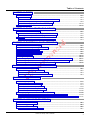
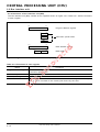
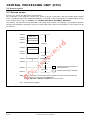
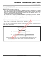
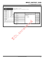
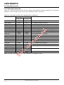
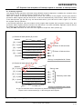
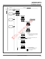
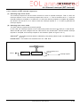
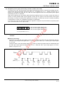
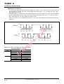
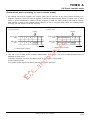
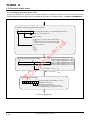
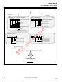
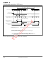
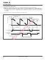
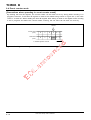
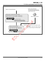
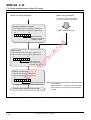
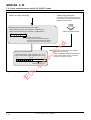
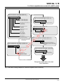
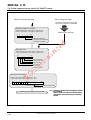
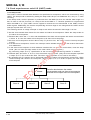
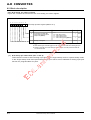
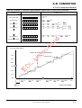
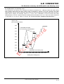
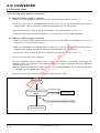
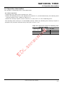
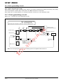
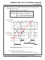
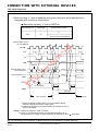
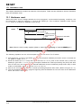
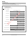
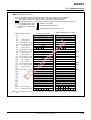
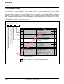
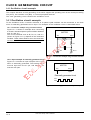
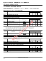
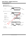
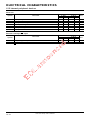
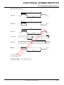
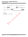
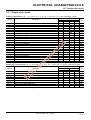
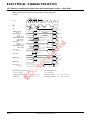
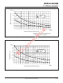
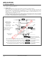
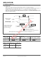
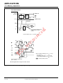
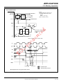
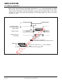
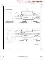
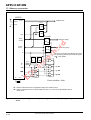
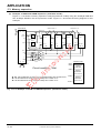
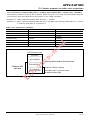
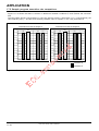
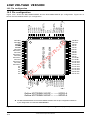
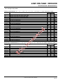
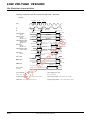
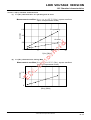
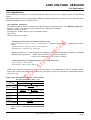
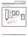
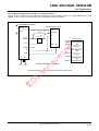
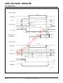
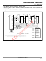
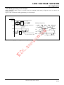
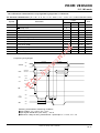
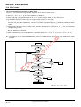
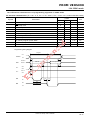
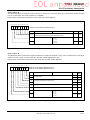
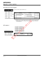
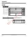
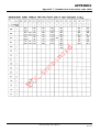
1
To all our customers
Regarding the change of names mentioned in the document, such as Mitsubishi
Electric and Mitsubishi XX, to Renesas Technology Corp.
The semiconductor operations of Hitachi and Mitsubishi Electric were transferred to Renesas
Technology Corporation on April 1st 2003. These operations include microcomputer, logic, analog
and discrete devices, and memory chips other than DRAMs (flash memory, SRAMs etc.)
Accordingly, although Mitsubishi Electric, Mitsubishi Electric Corporation, Mitsubishi
Semiconductors, and other Mitsubishi brand names are mentioned in the document, these names
have in fact all been changed to Renesas Technology Corp. Thank you for your understanding.
Except for our corporate trademark, logo and corporate statement, no changes whatsoever have been
made to the contents of the document, and these changes do not constitute any alteration to the
contents of the document itself.
Note : Mitsubishi Electric will continue the business operations of high frequency & optical devices
and power devices.
Renesas Technology Corp.
Customer Support Dept.
April 1, 2003
MITSUBISHI 16-BIT SINGLE-CHIP MICROCOMPUTER
7700 FAMILY / 7700 SERIES
7702/7703
Group
User’s Manual
Keep safety first in your circuit designs !
● Mitsubishi Electric Corporation puts the maximum effort into making semiconductor
products better and more reliable, but there is always the possibility that trouble
may occur with them. Trouble with semiconductors may lead to personal injury,
fire or property damage. Remember to give due consideration to safety when
making your circuit designs, with appropriate measures such as (i) placement
of substitutive, auxiliary circuits, (ii) use of non-flammable material or (iii) prevention
against any malfunction or mishap.
Notes regarding these materials
● These materials are intended as a reference to assist our customers in the
selection of the Mitsubishi semiconductor product best suited to the customer’s
application; they do not convey any license under any intellectual property rights,
or any other rights, belonging to Mitsubishi Electric Corporation or a third party.
● Mitsubishi Electric Corporation assumes no responsibility for any damage, or
infringement of any third-party’s rights, originating in the use of any product
data, diagrams, charts or circuit application examples contained in these materials.
● All information contained in these materials, including product data, diagrams
and charts, represent information on products at the time of publication of these
materials, and are subject to change by Mitsubishi Electric Corporation without
notice due to product improvements or other reasons. It is therefore recommended
that customers contact Mitsubishi Electric Corporation or an authorized Mitsubishi
Semiconductor product distributor for the latest product information before
purchasing a product listed herein.
● Mitsubishi Electric Corporation semiconductors are not designed or manufactured
for use in a device or system that is used under circumstances in which human
life is potentially at stake. Please contact Mitsubishi Electric Corporation or an
authorized Mitsubishi Semiconductor product distributor when considering the
use of a product contained herein for any specific purposes, such as apparatus
or systems for transportation, vehicular, medical, aerospace, nuclear, or undersea
repeater use.
● The prior written approval of Mitsubishi Electric Corporation is necessary to
reprint or reproduce in whole or in part these materials.
● If these products or technologies are subject to the Japanese export control
restrictions, they must be exported under a license from the Japanese government
and cannot be imported into a country other than the approved destination.
Any diversion or reexport contrary to the export control laws and regulations of
JAPAN and/or the country of destination is prohibited.
● Please contact Mitsubishi Electric Corporation or an authorized Mitsubishi
Semiconductor product distributor for further details on these materials or the
products contained therein.
Preface
This manual describes the hardware of the Mitsubishi
CMOS 16-bit microcomputers 7702 Group and 7703
Group. After reading this manual, the user will be
able to understand the functions, so that they can
utilize their capabilities fully.
For details concerning the software, refer to the 7700
Family Software Manual.
BEFORE USING THIS MANUAL
1. Constitution
This user’s manual consists of the following chapters. Refer to the chapters relevant to used products
and the processor mode.
●Chapter 1. DESCRIPTION to Chapter 17. APPLICATION
Functions which are common to all products and all processor modes are explained, using the
M37702M2BXXXFP as an example.
When there are functional differences between the low voltage version, PROM version and the 7703
Group, the referential section is indicated. Refer to that section about differences and to “Chapter. 1
to Chapter. 17” about the common functions.
●Chapter 18. LOW VOLTAGE VERSION
Refer to this chapter when using the products of which difference of electrical characteristics identification
code (see on page 1–2) is “L,” the M37702M2LXXXGP for example. This chapter mainly explains the
differences from the M37702M2BXXXFP, using the M37702M2LXXXGP as an example.
●Chapter 19. PROM VERSION
Refer to this chapter when using the products of which memory identification code (see on page 1–
2) is “E,” the M37702E2BXXXFP for example. This chapter mainly explains the differences from the
M37702M2BXXXFP, using the M37702E2BXXXFP as an example.
●Chapter 20. 7703 GROUP
Refer to this chapter when using the 7703 Group. This chapter mainly explains the differences from
the 7702 Group, using the M37703M2BXXXSP as an example.
●Appendix
Useful information for 7702 and 7703 Groups usage is shown.
2. Remark
●25 MHz version and 16 MHz version
The 25 MHz version products are distinguished from the 16 MHz version products in part of Chapters
as the case may be. Refer to it as follows:
•Products of which difference of electrical characteristics identification code is “B,” M37702M2BXXXFP
as an example ..................................................... Column of “25 MHz version”
•Products of which difference of electrical characteristics identification code is “A,” M37702M2AXXXFP
as an example ..................................................... Column of “16 MHz version”
●Product expansion
See the latest data book and data sheets. Additionally, ask the contact addresses on the last page.
●Electrical characteristics
See also the latest data book or data sheet.
●Development support tools
See the latest data book and data sheet.
●Software
See “7700 Family Software Manual.”
1
●Mask ROM Confirmation Form, PROM Confirmation Form, Mark Specification Form
Copy the form in the latest data book and use it. Or, ask the contact addresses on the last page.
3. Register structure
The view of the register structure is described below:
✽1
b7
b6
b5
b4
b3
✕ 0
b2
b1
b0
XXX register (Address XX16)
Bit
✽2
Bit name
Functions
✽3
At reset
RW
0
RW
Undefined
WO
0
RO
0
... select bit
0 : ...
1 : ...
1
... select bit
0 : ...
1 : ...
The value is “0” at reading.
2
... flag
0 : ...
1 : ...
3
Fix this bit to “0.”
0
RW
4
This bit is ignored in ... mode.
0
RW
Undefined
–
7 to 5 Nothing is assigned.
✽4
✽1
Blank
0
1
✕
: Set to “0” or “1” to meet the purpose.
: Set to “0” at writing.
: Set to “1” at writing.
: This bit is not used in the specific mode or state. It may be either “0” or “1.”
: Nothing is assigned.
✽2
0
: “0” immediately after a reset.
1
: “1” immediately after a reset.
Undefined :Undefined immediately after a reset.
✽3
RW
RO
WO
—
2
: It is possible to read the bit state at reading. The written value becomes valid
data.
: It is possible to read the bit state at reading. The written value becomes
invalid. Accordingly, the written value may be either “0” or “1.”
: The written value becomes valid data. It is not possible to read the bit state.
The value is undefined at reading. However, the bit with the commentaries of “
The value is “0” at reading” in the functions column or the notes is always “0”
at reading.(See to ✽4 above.)
: It is no possible to read the bit state. The value is undefined at reading.
However, the bit with the commentaries of “The value is “0” at reading” in the
functions column or the notes is always “0” at reading.(See to ✽4 above.)
The written value becomes invalid. Accordingly, the written value may be “0”
or “1.”
Table of Contents
Table of Contents
CHAPTER 1. DESCRIPTION
1.1 Performance overview.......................................................................................................... 1-3
1.2 Pin configuration ................................................................................................................... 1-4
1.3 Pin description ...................................................................................................................... 1-6
1.3.1 Example for processing unused pins .......................................................................... 1-9
1.4 Block diagram ...................................................................................................................... 1-12
CHAPTER 2. CENTRAL PROCESSING UNIT (CPU)
2.1 Central processing unit ....................................................................................................... 2-2
2.1.1 Accumulator (Acc) ......................................................................................................... 2-3
2.1.2 Index register X (X) ....................................................................................................... 2-3
2.1.3 Index register Y (Y) ....................................................................................................... 2-3
2.1.4 Stack pointer (S) ............................................................................................................ 2-4
2.1.5 Program counter (PC) ................................................................................................... 2-5
2.1.6 Program bank register (PG) ......................................................................................... 2-5
2.1.7 Data bank register (DT) ................................................................................................ 2-6
2.1.8 Direct page register (DPR) ........................................................................................... 2-6
2.1.9 Processor status register (PS) ..................................................................................... 2-8
2.2 Bus interface unit ............................................................................................................... 2-10
2.2.1 Overview ....................................................................................................................... 2-10
2.2.2 Functions of bus interface unit (BIU) ........................................................................ 2-12
2.2.3 Operation of bus interface unit (BIU)........................................................................ 2-14
2.3 Access space ....................................................................................................................... 2-16
2.3.1 Banks ............................................................................................................................ 2-17
2.3.2 Direct page ................................................................................................................... 2-17
2.4 Memory assignment ........................................................................................................... 2-18
2.4.1 Memory assignment in internal area ......................................................................... 2-18
2.5 Processor modes ................................................................................................................ 2-21
2.5.1 Single-chip mode ......................................................................................................... 2-22
2.5.2 Memory expansion and microprocessor modes ....................................................... 2-22
2.5.3 Setting processor modes ............................................................................................ 2-25
[Precautions when selecting processor mode]................................................................... 2-27
CHAPTER 3. INPUT/OUTPUT PINS
3.1 Programmable I/O ports ...................................................................................................... 3-2
3.1.1 Direction register ............................................................................................................ 3-3
3.1.2 Port register .................................................................................................................... 3-4
3.2 I/O pins of internal peripheral devices ............................................................................ 3-8
CHAPTER 4. INTERRUPTS
4.1 Overview .................................................................................................................................. 4-2
4.2 Interrupt sources ................................................................................................................... 4-4
7702/7703 Group User’s Manual
i
Table of Contents
4.3 Interrupt control .................................................................................................................... 4-6
4.3.1 Interrupt disable flag (I) ................................................................................................ 4-8
4.3.2 Interrupt request bit ....................................................................................................... 4-8
4.3.3 Interrupt priority level select bits and processor interrupt priority level (IPL) ....... 4-8
4.4 Interrupt priority level ........................................................................................................ 4-10
4.5 Interrupt priority level detection circuit ........................................................................ 4-11
4.6 Interrupt priority level detection time ............................................................................ 4-13
4.7 Sequence from acceptance of interrupt request to execution of interrupt routine ........................... 4-14
4.7.1 Change in IPL at acceptance of interrupt request .................................................. 4-16
4.7.2 Storing registers ........................................................................................................... 4-17
4.8 Return from interrupt routine ........................................................................................... 4-18
4.9 Multiple interrupts ...............................................................................................................
4-18
____
4.10 External interrupts
(INT
i interrupt) ................................................................................ 4-20
____
4.10.1 Function of INT i interrupt request
bit ...................................................................... 4-23
____
4.10.2 Switch of occurrence factor of INT i interrupt request ........................................... 4-25
4.11 Precautions when using interrupts............................................................................... 4-26
CHAPTER 5. TIMER A
5.1 Overview ..................................................................................................................................5-2
5.2 Block description .................................................................................................................. 5-3
5.2.1 Counter and reload register (timer Ai register) ......................................................... 5-4
5.2.2 Count start register ........................................................................................................ 5-5
5.2.3 Timer Ai mode register ................................................................................................. 5-6
5.2.4 Timer Ai interrupt control register ............................................................................... 5-7
5.2.5 Port P5 and port P6 direction registers ..................................................................... 5-8
5.3 Timer mode ............................................................................................................................ 5-9
5.3.1 Setting for timer mode ................................................................................................ 5-11
5.3.2 Count source ................................................................................................................ 5-13
5.3.3 Operation in timer mode ............................................................................................. 5-14
5.3.4 Select function ............................................................................................................. 5-15
5.4 Event counter mode ........................................................................................................... 5-19
5.4.1 Setting for event counter mode ................................................................................. 5-22
5.4.2 Operation in event counter mode .............................................................................. 5-24
5.4.3 Select functions ............................................................................................................ 5-26
5.5 One-shot pulse mode ......................................................................................................... 5-30
5.5.1 Setting for one-shot pulse mode ............................................................................... 5-32
5.5.2 Count source ................................................................................................................ 5-34
5.5.3 Trigger ........................................................................................................................... 5-35
5.5.4 Operation in one-shot pulse mode ............................................................................ 5-36
5.6 Pulse width modulation (PWM) mode ............................................................................ 5-39
5.6.1 Setting for PWM mode ............................................................................................... 5-41
5.6.2 Count source ................................................................................................................ 5-43
5.6.3 Trigger ........................................................................................................................... 5-43
5.6.4 Operation in PWM mode ............................................................................................ 5-44
CHAPTER 6. TIMER B
6.1 Overview ..................................................................................................................................6-2
6.2 Block description .................................................................................................................. 6-2
6.2.1 Counter and reload register (timer Bi register) ......................................................... 6-3
6.2.2 Count start register ........................................................................................................ 6-4
6.2.3 Timer Bi mode register ................................................................................................. 6-5
6.2.4 Timer Bi interrupt control register ............................................................................... 6-6
ii
7702/7703 Group User’s Manual
Table of Contents
6.2.5 Port P6 direction register ............................................................................................. 6-7
6.3 Timer mode ............................................................................................................................ 6-8
6.3.1 Setting for timer mode ................................................................................................ 6-10
6.3.2 Count source ................................................................................................................ 6-11
6.3.3 Operation in timer mode ............................................................................................. 6-12
6.4 Event counter mode ........................................................................................................... 6-14
6.4.1 Setting for event counter mode ................................................................................. 6-16
6.4.2 Operation in event counter mode .............................................................................. 6-17
6.5 Pulse period/pulse width measurement mode ............................................................. 6-19
6.5.1 Setting for pulse period/pulse width measurement mode ...................................... 6-21
6.5.2 Count source ................................................................................................................ 6-23
6.5.3 Operation in pulse period/pulse width measurement mode ................................... 6-24
CHAPTER 7. SERIAL I/O
7.1 Overview .................................................................................................................................. 7-2
7.2 Block description .................................................................................................................. 7-3
7.2.1 UARTi transmit/receive mode register ........................................................................ 7-4
7.2.2 UARTi transmit/receive control register 0 .................................................................. 7-6
7.2.3 UARTi transmit/receive control register 1 .................................................................. 7-7
7.2.4 UARTi transmit register and UARTi transmit buffer register ................................... 7-9
7.2.5 UARTi receive register and UARTi receive buffer register .................................... 7-11
7.2.6 UARTi baud rate register (BRGi) .............................................................................. 7-13
7.2.7 UARTi transmit interrupt control and UARTi receive interrupt control registers 7-14
7.2.8 Port P8 direction register ........................................................................................... 7-16
7.3 Clock synchronous serial I/O mode ............................................................................... 7-17
7.3.1 Transfer clock (synchronizing clock) ......................................................................... 7-18
7.3.2 Method of transmission ............................................................................................... 7-19
7.3.3 Transmit operation ....................................................................................................... 7-23
7.3.4 Method of reception .................................................................................................... 7-25
7.3.5 Receive operation ........................................................................................................ 7-29
7.3.6 Process on detecting overrun error ........................................................................... 7-32
[Precautions when operating in clock synchronous serial I/O mode] ............................. 7-33
7.4 Clock asynchronous serial I/O (UART) mode............................................................... 7-35
7.4.1 Transfer rate (frequency of transfer clock) .............................................................. 7-36
7.4.2 Transfer data format .................................................................................................... 7-38
7.4.3 Method of transmission ............................................................................................... 7-40
7.4.4 Transmit operation ....................................................................................................... 7-44
7.4.5 Method of reception .................................................................................................... 7-46
7.4.6 Receive operation ........................................................................................................ 7-49
7.4.7 Process on detecting error ......................................................................................... 7-51
7.4.8 Sleep mode .................................................................................................................. 7-52
[Precautions when operating in clock asynchronous serial I/O mode] ........................... 7-53
CHAPTER 8. A-D CONVERTER
8.1 Overview .................................................................................................................................. 8-2
8.2 Block description .................................................................................................................. 8-3
8.2.1 A-D control register ....................................................................................................... 8-4
8.2.2 A-D sweep pin select register ...................................................................................... 8-6
8.2.3 A-D register i (i = 0 to 7) ............................................................................................. 8-7
8.2.4 A-D conversion interrupt control register .................................................................... 8-8
8.2.5 Port P7 direction register ............................................................................................. 8-9
7702/7703 Group User’s Manual
iii
Table of Contents
8.3 A-D conversion method ..................................................................................................... 8-10
8.4 Absolute accuracy and differential non-linearity error .............................................. 8-12
8.4.1 Absolute accuracy ....................................................................................................... 8-12
8.4.2 Differential non-linearity error ..................................................................................... 8-13
8.5 One-shot mode .................................................................................................................... 8-14
8.5.1 Settings for one-shot mode ........................................................................................ 8-14
8.5.2 One-shot mode operation description ....................................................................... 8-16
8.6 Repeat mode ........................................................................................................................ 8-17
8.6.1 Settings for repeat mode ............................................................................................ 8-17
8.6.2 Repeat mode operation description .......................................................................... 8-19
8.7 Single sweep mode ............................................................................................................ 8-20
8.7.1 Settings for single sweep mode ................................................................................ 8-20
8.7.2 Single sweep mode operation description ................................................................ 8-22
8.8 Repeat sweep mode ........................................................................................................... 8-24
8.8.1 Settings for repeat sweep mode ............................................................................... 8-24
8.8.2 Repeat sweep mode operation description .............................................................. 8-26
8.9 Precautions when using A-D converter ......................................................................... 8-28
CHAPTER 9. WATCHDOG TIMER
9.1 Block description .................................................................................................................. 9-2
9.1.1 Watchdog timer .............................................................................................................. 9-3
9.1.2 Watchdog timer frequency select register .................................................................. 9-4
9.2 Operation description .......................................................................................................... 9-5
9.2.1 Basic operation .............................................................................................................. 9-5
9.2.2 Operation in Stop mode ............................................................................................... 9-7
9.2.3 Operation in Hold state ................................................................................................. 9-7
9.3 Precautions when using watchdog timer ........................................................................ 9-8
CHAPTER 10. STOP MODE
10.1 Clock generating circuit .................................................................................................. 10-2
10.2 Operation description ...................................................................................................... 10-3
10.2.1 Termination by interrupt request occurrence ......................................................... 10-4
10.2.2 Termination by hardware reset ................................................................................ 10-5
10.3 Precautions for Stop mode ............................................................................................ 10-6
CHAPTER 11. WAIT MODE
11.1 Clock generating circuit .................................................................................................. 11-2
11.2 Operation description ...................................................................................................... 11-3
11.2.1 Termination by interrupt request occurrence ......................................................... 11-4
11.2.2 Termination by hardware reset ................................................................................ 11-4
11.3 Precautions for Wait mode ............................................................................................. 11-5
CHAPTER 12. CONNECTION WITH EXTERNAL DEVICES
12.1 Signals required for accessing external devices ...................................................... 12-2
12.1.1 Descriptions of signals .............................................................................................. 12-2
12.1.2 Operation of bus interface unit (BIU) ..................................................................... 12-8
12.2 Software Wait ................................................................................................................... 12-11
12.3 Ready function ................................................................................................................ 12-13
12.3.1 Operation description .............................................................................................. 12-14
12.4 Hold function ................................................................................................................... 12-16
12.4.1 Operation description .............................................................................................. 12-17
iv
7702/7703 Group User’s Manual
Table of Contents
CHAPTER 13. RESET
13.1 Hardware reset .................................................................................................................. 13-2
13.1.1 Pin state ..................................................................................................................... 13-3
13.1.2 State of CPU, SFR area, and internal RAM area................................................. 13-4
13.1.3 Internal processing sequence
after reset ............................................................... 13-9
______
13.1.4 Time supplying “L” level to RESET pin ................................................................ 13-10
13.2 Software reset .................................................................................................................. 13-12
CHAPTER 14. CLOCK GENERATING CIRCUIT
14.1 Oscillation circuit example ............................................................................................. 14-2
14.1.1 Connection example using resonator/oscillator...................................................... 14-2
14.1.2 Input example of externally generated clock ......................................................... 14-2
14.2 Clock .................................................................................................................................... 14-3
14.2.1 Clock generated in clock generating circuit ........................................................... 14-4
CHAPTER 15. ELECTRICAL CHARACTERISTICS
15.1 Absolute maximum ratings ............................................................................................. 15-2
15.2 Recommended operating conditions ............................................................................ 15-3
15.3 Electrical characteristics ................................................................................................. 15-4
15.4 A-D converter characteristics ........................................................................................ 15-5
15.5 Internal peripheral devices ............................................................................................. 15-6
15.6 Ready and Hold ............................................................................................................... 15-12
15.7 Single-chip mode ............................................................................................................ 15-15
15.8 Memory expansion mode and microprocessor mode : with no Wait................ 15-17
15.9 Memory expansion mode and microprocessor
_ mode : with Wait ...................... 15-21
15.10 Testing circuit for ports P0 to P8, φ 1, and E ........................................................ 15-25
CHAPTER 16. STANDARD CHARACTERISTICS
16.1 Standard characteristics ................................................................................................. 16-2
16.1.1 Port standard characteristics .................................................................................... 16-2
16.1.2 I CC–f(XIN ) standard characteristics ............................................................................ 16-3
16.1.3 A–D converter standard characteristics .................................................................. 16-4
CHAPTER 17. APPLICATIONS
17.1 Memory expansion ............................................................................................................ 17-2
17.1.1 Memory expansion model ......................................................................................... 17-2
17.1.2 How to calculate timing ............................................................................................ 17-4
17.1.3 Points in memory expansion .................................................................................... 17-8
17.1.4 Example of memory expansion .............................................................................. 17-20
17.1.5 Example of I/O expansion ...................................................................................... 17-26
17.2 Sample program execution rate comparison ........................................................... 17-29
17.2.1 Difference depending on data bus width and software Wait .............................17-29
17.2.2 Comparison software Wait (f(X IN) = 20 MHz) with software Wait + Ready (f(XIN ) = 25 MHz) .. 17-31
CHAPTER 18. LOW VOLTAGE VERSION
18.1 Performance overview ..................................................................................................... 18-3
18.2 Pin configuration .............................................................................................................. 18-4
18.3 Functional description ..................................................................................................... 18-6
18.3.1 Power-on reset conditions ........................................................................................ 18-7
7702/7703 Group User’s Manual
v
Table of Contents
18.4 Electrical characteristics ................................................................................................. 18-8
18.4.1 Absolute maximum ratings ....................................................................................... 18-8
18.4.2 Recommended operating conditions ....................................................................... 18-9
18.4.3 Electrical characteristics ......................................................................................... 18-10
18.4.4 A-D converter characteristics ................................................................................. 18-11
18.4.5 Internal peripheral devices ..................................................................................... 18-12
18.4.6 Ready and Hold ....................................................................................................... 18-18
18.4.7 Single-chip mode ..................................................................................................... 18-21
18.4.8 Memory expansion mode and microprocessor mode : with no Wait ............... 18-23
18.4.9 Memory expansion mode and microprocessor_ mode : with Wait ..................... 18-27
18.4.10 Testing circuit for ports P0 to P8, φ 1, and E ................................................... 18-31
18.5 Standard characteristics ............................................................................................... 18-32
18.5.1 Port standard characteristics .................................................................................. 18-32
18.5.2 I CC –f(XIN) standard characteristics .......................................................................... 18-33
18.5.3 A–D converter standard characteristics ................................................................ 18-34
18.6 Application ....................................................................................................................... 18-35
18.6.1 Memory expansion ................................................................................................... 18-35
18.6.2 Memory expansion example on minimum model ................................................ 18-37
18.6.3 Memory expansion example on medium model A .............................................. 18-39
18.6.4 Memory expansion example on maximum model ............................................... 18-41
18.6.5 Ready generating circuit example ......................................................................... 18-43
CHAPTER 19. PROM VERSION
19.1 Overview ............................................................................................................................. 19-2
19.2 EPROM mode ..................................................................................................................... 19-4
19.2.1 Write method .............................................................................................................. 19-4
19.2.2 Pin description ........................................................................................................... 19-5
19.3 1M mode ............................................................................................................................. 19-6
19.3.1 Read/Program/Erase ................................................................................................. 19-9
19.3.2 Programming algorithm of 1M mode ..................................................................... 19-10
19.3.3 Electrical characteristics of programming algorithm in 1M mode ..................... 19-11
19.4 256K mode ........................................................................................................................ 19-12
19.4.1 Read/Program/Erase ............................................................................................... 19-15
19.4.2 Programming algorithm of 256K mode ................................................................. 19-16
19.4.3 Electrical characteristics of programming algorithm in 256K mode ................. 19-17
19.5 Usage precaution ............................................................................................................ 19-18
19.5.1 Precautions on all PROM versions ....................................................................... 19-18
19.5.2 Precautions on One time PROM version ............................................................. 19-18
19.5.3 Precautions on EPROM version ............................................................................ 19-18
19.5.4 Bus timing and EPROM mode ............................................................................... 19-19
CHAPTER 20. 7703 GROUP
20.1 Description ......................................................................................................................... 20-2
20.2 Performance overview ..................................................................................................... 20-3
20.3 Pin configuration .............................................................................................................. 20-4
20.4 Functional description ..................................................................................................... 20-5
20.4.1 I/O pin ......................................................................................................................... 20-6
20.4.2 Timer A ....................................................................................................................... 20-7
20.4.3 Timer B ....................................................................................................................... 20-7
20.4.4 Serial I/O .................................................................................................................... 20-8
20.4.5 A-D converter ........................................................................................................... 20-10
vi
7702/7703 Group User’s Manual
Table of Contents
20.5 Electrical characteristics ............................................................................................... 20-12
20.6 PROM version .................................................................................................................. 20-13
20.6.1 EPROM mode .......................................................................................................... 20-13
20.6.2 Bus timing and EPROM mode ............................................................................... 20-15
APPENDIX
Appendix
Appendix
Appendix
Appendix
Appendix
Appendix
Appendix
Appendix
1.
2.
3.
4.
5.
6.
7.
8.
Memory assignment ........................................................................................... 21-2
Memory assignment in SFR area ................................................................... 21-7
Control registers ............................................................................................... 21-11
Package outlines .............................................................................................. 21-32
Countermeasures against noise ................................................................... 21-35
Q & A .................................................................................................................. 21-45
Hexadecimal instruction code table ............................................................. 21-55
Machine instructions ....................................................................................... 21-58
GLOSSARY
7702/7703 Group User’s Manual
vii
Table of Contents
MEMORANDUM
viii
7702/7703 Group User’s Manual
CHAPTER 1
DESCRIPTION
1.1
1.2
1.3
1.4
Performance overview
Pin configuration
Pin description
Block diagram
DESCRIPTION
The 16-bit single-chip microcomputers 7702 Group and 7703 Group are suitable for office, business, and
industrial equipment controllers that require high-speed processing of large amounts of data.
These microcomputers develop with the M37702M2BXXXFP as the base chip. This manual describes the
functions about the M37702M2BXXXFP unless there is a specific difference and refers to the M37702M2BXXXXFP
as “M37702.”
Notes 1: About details concerning each microcomputer’s development status of the 7702/7703 Group,
inquire of “CONTACT ADDRESSES FOR FURTHER INFORMATION” described last.
Notes 2: How the 7702/7703 Group’s type name see is described below.
M 3 77 02 M 2 B XXX FP
Mitsubishi integrated prefix
Represent an original single-chip microcomputer
Series designation using 2 digits
Circuit function identification code using 2 digits
Memory identification code using a digit
M: Mask ROM
E: EPROM
S: External ROM
Memory size identification code using a digit
Difference of electrical characteristics identification code
using a digit
Mask ROM number
Package style
FP: Plastic molded QFP
GP: Plastic molded QFP
HP: Plastic molded fine-pitch QFP
SP: Plastic molded SDIP
FS: Ceramic QFN
1–2
7702/7703 Group User’s Manual
DESCRIPTION
1.1 Performance overview
1.1 Performance overview
Table 1.1.1 shows the performance overview of the M37702.
7703 Group
Refer to “Chapter 20. 7703 GROUP.”
Table 1.1.1 M37702 performance overview
Parameters
Number of basic instructions
M37702M2BXXXFP
Instruction execution time
M37702M2AXXXFP
External clock input frequency M37702M2BXXXFP
M37702M2AXXXFP
f(XIN)
ROM
Memory size
RAM
Programmable Input/Output
ports
Multifunction timers
Serial I/O
A-D converter
Watchdog timer
Interrupts
Clock generating circuit
Supply voltage
Power dissipation
Port Input/Output
characteristics
Memory expansion
Operating temperature range
P0–P2, P4–P8
P3
TA0–TA4
TB0–TB2
UART0, UART1
Functions
103
160 ns (the minimum instruction at f(X IN) = 25 MHz)
250 ns (the minimum instruction at f(X IN) = 16 MHz)
25 MHz (maximum)
16 MHz (maximum)
16384 bytes
512 bytes
8 bits ✕ 8
4 bits ✕ 1
16 bits ✕ 5
16 bits ✕ 3
(UART or clock synchronous serial I/O) ✕ 2
8-bit successive approximation method ✕ 1 (8 channels)
12 bits ✕ 1
3 external, 16 internal (priority levels 0 to 7 can
be set for each interrupt with software)
Built-in (externally connected to a ceramic
resonator or a quartz-crystal oscillator)
5 V ±10 %
60 mW (at f(X IN) = 16 MHz frequency, typ.)
Input/Output withstand voltage 5 V
5 mA
Output current
Maximum 16 Mbytes
–20°C to 85°C
CMOS high-performance silicon gate process
Device structure
Package
80-pin plastic molded QFP
Notes 1: All of the 7702 Group microcomputers are the same except for the package type, memory type,
memory size, and electric characteristics.
2: For the low voltage version, refer to “Chapter 18. LOW VOLTAGE VERSION.”
7702/7703 Group User’s Manual
1–3
DESCRIPTION
1.2 Pin configuration
1.2 Pin configuration
Figure 1.2.1 shows the M37702M2BXXXFP pin configuration. Figure 1.2.2 shows the M37702M2BXXXHP
pin configuration.
Note: For the low voltage version of the 7702 Group, refer to “Chapter 18. LOW VOLTAGE VERSION.”
P71/AN1
P72/AN2
P73/AN3
P74/AN4
P75/AN5
P76/AN6
P77/AN7/ADTRG
VSS
AVSS
VREF
AVCC
VCC
P80/CTS0/RTS0
P81/CLK0
P82/RXD0
P83/TXD0
7703 Group
Refer to “Chapter 20. 7703 GROUP.”
80 79 78 77 76 75 74 73 72 71 70 69 68 67 66 65
1
64
2
63
3
62
4
5
6
7
8
9
10
11
12
13
14
15
16
17
18
19
20
21
22
M37702M2BXXXFP
P70/AN0
P67/TB2IN
P66/TB1IN
P65/TB0IN
P64/INT2
P63/INT1
P62/INT0
P61/TAIN
P60/TA4OUT
P57/TA3IN
P56/TA3OUT
P55/TA2IN
P54/TA2OUT
P53/TA1IN
P52/TA1OUT
P51/TA0IN
P50/TA0OUT
P47
P46
P45
P44
P43
P42/ 1
P41/RDY
60
59
58
57
56
55
54
53
52
51
50
49
48
47
46
45
44
43
23
42
24
41
P40/HOLD
BYTE
CNVSS
RESET
XIN
XOUT
E
Vss
P33/HLDA
P32/ALE
P31/BHE
P30/R/W
P27/A23/D7
P26/A22/D6
P25/A21/D5
P24/A20/D4
25 26 27 28 29 30 31 32 33 34 35 36 37 38 39 40
Outline 80P6N-A
Fig. 1.2.1 M37702M2BXXXFP pin configuration (top view)
1–4
61
7702/7703 Group User’s Manual
P84/CTS1/RTS1
P85/CLK1
P86/RXD1
P87/TXD1
P00/A0
P01/A1
P02/A2
P03/A3
P04/A4
P05/A5
P06/A6
P07/A7
P10/A8/D8
P11/A9/D9
P12/A10/D10
P13/A11/D11
P14/A12/D12
P15/A13/D13
P16/A14/D14
P17/A15/D15
P20/A16/D0
P21/A17/D1
P22/A18/D2
P23/A19/D3
DESCRIPTION
1.2 Pin configuration
P67/TB2IN
P70/AN0
P71/AN1
P72/AN2
P73/AN3
P74/AN4
P75/AN5
P76/AN6
P77/AN7/ADTRG
VSS
AVSS
VREF
AVCC
VCC
P80/CTS0/RTS0
P81/CLK0
P82/RXD0
P83/TXD0
P84/CTS1/RTS1
P85/CLK1
✽
✽
80 79 78 77 76 75 74 73 72 71 70 69 68 67 66 65 64 63 62 61
1
60
2
59
3
58
4
57
5
56
M37702M2BXXXHP
P66/TB1IN
P65/TB0IN
P64/INT2
P63/INT1
P62/INT0
P61/TA4IN
P60/TA4OUT
P57/TA3IN
P56/TA3OUT
P55/TA2IN
P54/TA2OUT
P53/TA1IN
P52/TA1OUT
P51/TA0IN
P50/TA0OUT
P47
P46
P45
P44
P43
6
7
8
9
10
11
12
13
14
15
16
17
55
54
53
52
51
50
49
48
47
46
45
44
18
43
19
42
20
41
P86/RxD1
P87/TxD1
P00/A0
P01/A1
P02/A2
P03/A3
P04/A4
P05/A5
P06/A6
P07/A7
P10/A8/D8
P11/A9/D9
P12/A10/D10
P13/A11/D11
P14/A12/D12
P15/A13/D13
P16/A14/D14
P17/A15/D15
P20/A16/D0
P21/A17/D1
P42/ 1
P41/RDY
P40/HOLD
BYTE
CNVSS
RESET
XIN
XOUT
E
VSS
P33/HLDA
P32/ALE
P31/BHE
P30/R/W
P27/A23/D7
P26/A22/D6
P25/A21/D5
P24/A20/D4
P23/A19/D3
P22/A18/D2
21 22 23 24 25 26 27 28 29 30 31 32 33 34 35 36 37 38 39 40
✽
✽
Outline 80P6D-A
✽ : The M37702M2BXXXHP have the pin configuration shifted to 2 pins assignment
from the M37702M2BXXXFP.
Fig. 1.2.2 M37702M2BXXXHP pin configuration (top view)
7702/7703 Group User’s Manual
1–5
DESCRIPTION
1.3 Pin description
1.3 Pin description
Tables 1.3.1 to 1.3.3 list the pin description. However, the pin description in the EPROM mode of the builtin PROM version is described to section “19.2 EPROM mode.”
7703 Group
The 7703 Group does not have part of pins. Refer to “Chapter 20. 7703 GROUP.”
Table 1.3.1 Pin description (1)
Pin
Vcc, Vss
CNVss
Name
Power supply
CNVss
Input/Output
Input
______
RESET
Reset input
Input
X IN
Clock input
Input
X OUT
Clock output
Output
E
Enable output
Output
BYTE
B u s w i d t h s e l e c t i o n Input
input
_
AVcc
AVss
Analog supply
Functions
Supply 5 V ±10 % to Vcc pin and 0 V to Vss pin.
This pin controls the processor mode.
✽
[Single-chip mode] [Memory expansion mode]
Connect to Vss pin.
[Microprocessor mode]
Connect to Vcc pin.
The microcomputer is reset when supplying “L” level
to this pin.
These are I/O pins of the internal clock generating
circuit. Connect a ceramic resonator or quartz-crystal
oscillator between pins X IN and XOUT . When using an
external clock, the clock source should be input to X IN
pin and X OUT pin _
should be left open.
This pin outputs E signal.
Data/instruction code read or data write is performed
when output from this pin is “L” level.
[Single-chip mode]
Connect to Vss.
[Memory expansion mode] [Microprocessor mode]
Input level to this pin determines whether the external
data bus has a 16-bit width or 8-bit width. The width
is 16 bits when the level is “L”, and 8 bits when the
level is “H”.
The power supply pin for the A-D converter. Externally
connect AVcc to Vcc pin.
The power supply pin for the A-D converter. Externally
connect AVss to Vss pin.
This is a reference voltage input pin for the A-D converter.
Reference voltage input Input
V REF
✽ : In the low voltage version, supply 2.7–5.5V to Vcc.
1–6
7702/7703 Group User’s Manual
DESCRIPTION
1.3 Pin description
Table 1.3.2 Pin description (2)
Pin
P00–P07
Name
I/O port P0
A 0–A 7
P10–P17
Input/Output
I/O
Output
I/O port P1
I/O
I/O port P2
Data (D8 to D15 ) input/output and output of the middleorder 8 bits (A8–A 15 ) of the address are performed
with the time sharing system.
[Single-chip mode]
Port P2 is an 8-bit I/O port with the same function as P0.
[Memory expansion mode] [Microprocessor mode]
I/O
A 16/D0–
A 23/D7
P30–P33✽
I/O port P3
Data (D 0 to D7) input/output and output of the highorder 8 bits (A 16–A 23) of the address are performed
with the time sharing system.
[Single-chip mode]
Port P3 is a 4-bit I/O port with the same function as P0.
[Memory expansion mode] [Microprocessor
mode]
__ ____
_____
P30–P3 3 respectively output R/W, BHE, ALE, and HLDA
signals.
__
I/O
__
R/W,
____
BHE,
ALE,
_____
[Single-chip mode]
Port P0 is an 8-bit CMOS I/O port. This port has an
I/O direction register and each pin can be programmed
for input or output.
[Memory expansion mode] [Microprocessor mode]
Low-order 8 bits (A 0–A7) of the address are output.
[Single-chip mode]
Port P1 is an 8-bit I/O port with the same function as
P0.
[Memory expansion mode] [Microprocessor mode]
●External bus width = 8 bits (When the BYTE pin is
“H” level)
Middle-order 8 bits (A8–A15) of the address are output.
●External bus width = 16 bits (When the BYTE pin is
“L” level)
A 8/D 8–
A 15/D15
P20–P27
Functions
Output
●R/W
The Read/Write signal indicates the data bus state.
The state is read while this signal is “H” level, and
write
while this signal is “L” level.
____
●BHE
“L” level is output when an odd-numbered address is
accessed.
●ALE
HLDA✽
This is used to obtain only the address from address
and
data multiplex signals.
_____
●HLDA
This is the signal to externally indicate the state when
the microcomputer is in Hold state.
“L” level is output during Hold state.
_____
✼ : The 7703 Group does not have the P3 3/HLDA pin.
7702/7703 Group User’s Manual
1–7
DESCRIPTION
1.3 Pin description
Table 1.3.3 Pin description (3)
Pin
P4 0–P4 7✼
Name
I/O port P4
Input/Output
I/O
_____
Input
Input
I/O
HOLD,
____
RDY,
P4 2–P4 7✼
_____
Input
Input
Output
I/O
HOLD,
____
RDY,
φ1,
P4 3–P4 7✼
P5 0–P5 7
I/O port P5
I/O
P6 0–P6 7✼
I/O port P6
I/O
P7 0–P7 7✼
I/O port P7
I/O
P8 0–P8 7✼
I/O port P8
I/O
✼ : The 7703 Group does not have the
1–8
Functions
[Single-chip mode]
Port P4 is an 8-bit I/O port with the same function as
P0. P42 can be programmed as the clock φ1 output pin.
[Memory expansion _____
mode]
____
P4 0 functions as the HOLD input pin, P41 as the RDY
input pin. The microcomputer
is in Hold state while “L”
_____
level is input to the HOLD pin.
The microcomputer
is in Ready state while “L” level is
____
input to the RDY pin.
P4 2–P47 function as I/O ports with the same functions
as P0.
P4 2 can be programmed for the clock φ1 output pin.
[Microprocessor mode]
_____
____
P4 0 functions as the HOLD input pin, P41 as the RDY
input pin. P42 always functions as the clock φ1 output
pin.
P4 3–P47 function as I/O ports with the same functions
as P0.
Port P5 is an 8-bit I/O port with the same function as
P0. These pins can be programmed as I/O pins for
Timers A0–A3.
Port P6 is an 8-bit I/O port with the same function as
P0. These pins can be programmed as I/O pins for
Timer A4, input pins for external interrupt and input
pins for Timers B0–B2.
Port P7 is an 8-bit I/O port with the same function as
P0. These pins can be programmed as input pins for
A-D converter.
Port P8 is an 8-bit I/O port with the same function as
P0. These pins can be programmed as I/O pins for
Serial I/O.
P4 3–P4 6, P60, P6 1, P6 6, P67, P73–P7 6, P84, and P85 pins.
7702/7703 Group User’s Manual
DESCRIPTION
1.3 Pin description
1.3.1 Example for processing unused pins
Examples for processing unused pins are described below. These descriptions are just examples. The user
shall modify them according to the user’s actual application and test them.
(1) In single-chip mode
Table 1.3.4 Example for processing unused pins in single-chip mode
Pin name
Example of processing
Ports P0 to P8
Set for input mode and connect these pins to Vcc or
Vss via a resistor; or set for output mode and leave
these pins open. (Notes 1, 3)
Leave it open.
_
E
X OUT (Note 2)
Connect this pin to Vcc.
Connect these pins to Vss.
AVcc
AVss, V REF, BYTE
Notes 1: When setting these ports to the output mode and leave them open, they remain set to the input
mode until they are switched to the output mode by software after reset. While ports remain set
to the input mode, consequently, voltage levels of pins are unstable, and a power source current
can increase.
The contents of the direction register can be changed by noise or a program runaway generated
by noise. To improve its reliability, we recommend to periodically set the contents of the direction
register by software.
When processing unused pins, use the possible shortest wiring (within 20 mm from the microcomputer).
2: This applies when a clock externally generated is input to the XIN pin.
3: In the 7703 Group, the following ports does not have the corresponding pins and have only the
direction registers. Fix the bit of these direction registers to “1” (output mode).
•Ports P3 3, P43–P4 6, P60, P61, P66, P67, P7 3–P7 6, P84, P85
● When setting ports for input mode
● When setting ports for output mode
P0–P8
E
XOUT
Left open
M37702
M37702
VCC
AVCC
AVSS
VREF
P0–P8
Left open
E
XOUT
Left open
VCC
AVCC
AVSS
VREF
BYTE
BYTE
VSS
VSS
Fig. 1.3.1 Example for processing unused pins in single-chip mode
7702/7703 Group User’s Manual
1–9
DESCRIPTION
1.3 Pin description
(2) In memory expansion mode
Table 1.3.5 Example for processing unused pins in memory expansion mode
Pin name
Example of processing
Ports P4 2 to P4 7, P5 to P8
Set for input mode and connect these pins to Vcc or
Vss via a resistor; or set for output mode and leave
these pins open. (Notes 1, 6, 7)
____
BHE (Note 2)
Leave them open. (Note 4)
ALE (Note 3)
HLDA (Note 6)
X
OUT (Note 5)
_____
____
HOLD, RDY (Note 8)
AVcc
_____
Leave it open.
Connect these pins to Vcc via a resistor (pull-up).
Connect this pin to Vcc.
Connect these pins to Vss.
AVss, V REF
Notes 1: When setting these ports to the output mode and leave them open, they remain set to the input
mode until they are switched to the output mode by software after reset. While ports remain set
to the input mode, consequently, voltage levels of pins are unstable, and a power source current can increase.
The contents of the direction register can be changed by noise or a program runaway generated
by noise. To improve its reliability, we recommend to periodically set the contents of the direction
register by software.
When processing unused pins, use the possible shortest wiring (within 20 mm from the microcomputer).
2: This applies when “H” level is input to the BYTE pin.
3: This applies when “H” level is input to the BYTE pin and the access space is 64 Kbytes.
4: When supplying Vss level to the CNVss pin, these pins remain set to the input mode until they
are switched to the output mode by software after reset. While pins remain set to the input mode,
consequently, voltage levels of pins are unstable, and a power source current can increase.
5: This applies when a clock externally generated is input to the XIN pin.
6: In the 7703 Group, the following ports does not have the corresponding pins and have only the
direction registers. Fix the bit of these direction registers to “1” (output mode).
•Ports P4 3–P4 6,_____
P60, P61, P66, P67, P7 3–P7 6, P84, P85
There is not the HLDA pin.
7: Set the P42/φ1 pin to the P4 2 function (clock φ1 output disabled), and perform the same processing
as ports P43–P47, P5–P8.
8: When processing unused pins, use the possible shortest wiring (within 20 mm from the microcomputer).
● When setting ports for input mode
P42–P47, P5–P8
Left open
XOUT
Left open
P42–P47, P5–P8
Left open
BHE
ALE
HLDA
Left open
XOUT
Left open
M37702
M37702
BHE
ALE
HLDA
● When setting ports for output mode
VCC
VCC
HOLD
RDY
HOLD
RDY
AVCC
AVSS
VREF
AVCC
AVSS
VREF
VSS
Fig. 1.3.2 Example for processing unused pins in memory expansion mode
1–10
7702/7703 Group User’s Manual
VSS
DESCRIPTION
1.3 Pin description
(3) In microprocessor mode
Table 1.3.6 Example for processing unused pins in microprocessor mode
Example of processing
Pin name
Set for input mode and connect these pins to Vcc or
Ports P4 3 to P47, P5 to P8
Vss via a resistor; or set for output mode and leave
these pins open. (Notes 1, 6)
____
Leave it open. (Note 4)
BHE (Note 2)
ALE (Note 3)
HLDA, φ1 (Note 6)
X
OUT (Note 5)
_____
____
HOLD, RDY (Note 7)
AVcc
_____
Leave it open.
Connect these pins to Vcc via a resistor (pull-up).
Connect this pin to Vcc.
Connect these pins to Vss.
AVss, V REF
Notes 1: When setting these ports to the output mode and leave them open, they remain set to the input
mode until they are switched to the output mode by software after reset. While ports remain set
to the input mode, consequently, voltage levels of pins are unstable, and a power source current
can increase.
The contents of the direction register can be changed by noise or a program runaway generated
by noise. To improve its reliability, we recommend to periodically set the contents of the direction
register by software.
When processing unused pins, use the possible shortest wiring (within 20 mm from the microcomputer).
2: This applies when “H” level is input to the BYTE pin.
3: This applies when “H” level is input to the BYTE pin and the access space is 64 Kbytes.
4: When supplying Vss level to the CNVss pin, these pins remain set to the input mode until they
are switched to the output mode by software after reset. While pins remain set to the input mode,
consequently, voltage levels of pins are unstable, and a power source current can increase.
5: This applies when a clock externally generated is input to the X IN pin.
6: In the 7703 Group, the following ports does not have the corresponding pins and have only the
direction registers. Fix the bit of these direction registers to “1” (output mode).
•Ports P43–P4 6,_____
P6 0, P61, P66, P67, P73–P7 6, P84, P85
There is not the HLDA pin.
7: When processing unused pins, use the possible shortest wiring (within 20 mm from the microcomputer).
● When setting ports for input mode
P43–P47, P5–P8
Left open
BHE
ALE
HLDA
Left open
Left open
1
XOUT
P43–P47, P5–P8
M37702
M37702
BHE
ALE
HLDA
● When setting ports for output mode
Left open
VCC
1
XOUT
Left open
VCC
HOLD
RDY
HOLD
RDY
AVCC
AVCC
AVSS
VREF
AVSS
VREF
VSS
VSS
Fig. 1.3.3 Example for processing unused pins in microprocessor mode
7702/7703 Group User’s Manual
1–11
DESCRIPTION
1.4 Block diagram
1.4 Block diagram
External data bus width
selection input
BYTE
Figure 1.4.1 shows the M37702 block diagram.
Data Bus(Even)
P0(8)
Instruction Queue Buffer Q0(8)
Accumulator B(16)
Input/Output
port P2
Input/Output
port P3
Input/Output
port P4
Input/Output
port P5
P2(8)
P3(4)
P4(8)
P7(8)
Input/Output
port P7
P8(8)
Input/Output
port P8
Arithmetic Logic
Unit(16)
Note: The 7703 Group does not have the P33, P43–P46, P60, P61, P66, P67, P73–P76, P84, and P85 pins.
Fig. 1.4.1 M37702 block diagram
1–12
P5(8)
A-D Converter(8)
UART0(9)
UART1(9)
RAM
512 bytes
ROM
16 Kbytes
Accumulator A(16)
Clock Generating Circuit
Clock input
XIN
Clock output
XOUT
Enable output
E
Index Register X(16)
P6(8)
Index Register Y(16)
Timer TA4(16)
Stack Pointer S(16)
Timer TB0(16)
Direct Page Register DPR(16)
Timer TA0(16)
Reset input
RESET
Processor Status Register PS(11)
Timer TB2(16)
Input Buffer Register IB(16)
Timer TB1(16)
VCC
Data Bank Register DT(8)
Timer TA1(16)
Program Bank Register PG(8)
Watchdog Timer
(0V)
VSS
Program Counter PC(16)
Timer TA2(16)
Incrementer/Decrementer(24)
Timer TA3(16)
CNVss
Data Address Register DA(24)
Central Processing Unit (CPU)
(0V)
AVSS
Program Address Register PA(24)
Bus
Interface
Unit
(BIU)
Address Bus
Incrementer(24)
Input/Output
port P6
P1(8)
Instruction Queue Buffer Q2(8)
Input/Output
port P1
Instruction Queue Buffer Q1(8)
AVCC
Reference
voltage input
VREF
Instruction Register(8)
Data Buffer DBL(8)
Input/Output
port P0
Data Bus(Odd)
Data Buffer DBH(8)
7702/7703 Group User’s Manual
CHAPTER 2
CENTRAL
PROCESSING UNIT
(CPU)
2.1
2.2
2.3
2.4
2.5
Central processing unit
Bus interface unit
Access space
Memory assignment
Processor modes
CENTRAL PROCESSING UNIT (CPU)
2.1 Central processing unit
2.1 Central processing unit
The CPU (Central Processing Unit) has the ten registers as shown in Figure 2.1.1.
b15
b0
b8 b7
AH
b15
b0
b8 b7
BH
b15
Accumulator B (B)
BL
b0
b8 b7
XH
Index register X (X)
XL
b15
b0
b8 b7
YH
b15
YL
Index register Y (Y)
b0
b8 b7
SH
b7
Accumulator A (A)
AL
Stack pointer (S)
SL
b0
Data bank register (DT)
DT
b16 b15
b23
b8 b7
PG
b0
PCH
b7
Program counter (PC)
PCL
b0
Program bank register (PG)
b15
b0
b8 b7
DPRH
b15
DPRL
b0
b8 b7
PSH
b15
0
b10
0
0
0
0
Direct page register (DPR)
b9 b8 b7 b6
IPL
N V
Processor status register (PS)
PSL
b5 b4 b3 b2
b1
b0
m
Z
C
x
D
I
Carry flag
Zero flag
Interrupt disable flag
Decimal mode flag
Index register length flag
Data length flag
Overflow flag
Negative flag
Processor interrupt priority level
Fig. 2.1.1 CPU registers structure
2–2
7702/7703 Group User’s Manual
CENTRAL PROCESSING UNIT (CPU)
2.1 Central processing unit
2.1.1 Accumulator (Acc)
Accumulators A and B are available.
(1) Accumulator A (A)
Accumulator A is the main register of the microcomputer. The transaction of data such as calculation,
data transfer, and input/output are performed mainly through accumulator A. It consists of 16 bits,
and the low-order 8 bits can also be used separately. The data length flag (m) determines whether
the register is used as a 16-bit register or as an 8-bit register. Flag m is a part of the processor status
register which is described later. When an 8-bit register is selected, only the low-order 8 bits of
accumulator A are used and the contents of the high-order 8 bits is unchanged.
(2) Accumulator B (B)
Accumulator B is a 16-bit register with the same function as accumulator A. Accumulator B can be
used instead of accumulator A. The use of accumulator B, however except for some instructions,
requires more instruction bytes and execution cycles than that of accumulator A. Accumulator B is
also controlled by the data length flag (m) just as in accumulator A.
2.1.2 Index register X (X)
Index register X consists of 16 bits and the low-order 8 bits can also be used separately. The index register
length flag (x) determines whether the register is used as a 16-bit register or as an 8-bit register. Flag x
is a part of the processor status register which is described later. When an 8-bit register is selected, only
the low-order 8 bits of index register X are used and the contents of the high-order 8 bits is unchanged.
In an addressing mode in which index register X is used as an index register, the address obtained by
adding the contents of this register to the operand’s contents is accessed.
In the MVP or MVN instruction, a block transfer instruction, the contents of index register X indicates the
low-order 16 bits of the source address. The third byte of the instruction is the high-order 8 bits of the
source address.
Note: Refer to “7700 Family Software Manual” for addressing modes.
2.1.3 Index register Y (Y)
Index register Y is a 16-bit register with the same function as index register X. Just as in index register
X, the index register length flag (x) determines whether this register is used as a 16-bit register or as an
8-bit register.
In the MVP or MVN instruction, a block transfer instruction, the contents of index register Y indicate the
low-order 16 bits of the destination address. The second byte of the instruction is the high-order 8 bits of
the destination address.
7702/7703 Group User’s Manual
2–3
CENTRAL PROCESSING UNIT (CPU)
2.1 Central processing unit
2.1.4 Stack pointer (S)
The stack pointer (S) is a 16-bit register. It is used for a subroutine call or an interrupt. It is also used when
addressing modes using the stack are executed. The contents of S indicate an address (stack area) for
storing registers during subroutine calls and interrupts. Bank 016 is specified for the stack area. (Refer to
“2.1.6 Program bank register (PG).”)
When an interrupt request is accepted, the microcomputer stores the contents of the program bank register
(PG) at the address indicated by the contents of S and decrements the contents of S by 1. Then the
contents of the program counter (PC) and the processor status register (PS) are stored. The contents of
S after accepting an interrupt request is equal to the contents of S decremented by 5 before the accepting
of the interrupt request. (Refer to Figure 2.1.2.)
When completing the process in the interrupt routine and returning to the original routine, the contents of
registers stored in the stack area are restored into the original registers in the reverse sequence (PS→PC→PG)
by executing the RTI instruction. The contents of S is returned to the state before accepting an interrupt
request.
The same operation is performed during a subroutine call, however, the contents of PS is not automatically
stored. (The contents of PG may not be stored. This depends on the addressing mode.)
The user should store registers other than those described above with software when the user needs them
during interrupts or subroutine calls.
Additionally, initialize S at the beginning of the program because its contents are undefined at reset. The
stack area changes when subroutines are nested or when multiple interrupt requests are accepted. Therefore,
make sure of the subroutine’s nesting depth not to destroy the necessary data.
Note: Refer to “7700 Family Software Manual” for addressing modes.
Stack area
Address
S–5
S–4
Processor status register’s low-order byte (PSL)
S–3 Processor status register’s high-order byte (PSH)
S–2
Program counter’s low-order byte (PCL)
S–1
Program counter’s high-order byte (PCH)
S
Program bank register (PG)
● “S” is the initial address that the stack pointer (S)
indicates at accepting an interrupt request.
The S’s contents become “S–5” after storing the
above registers.
Fig. 2.1.2 Stored registers of the stack area
2–4
7702/7703 Group User’s Manual
CENTRAL PROCESSING UNIT (CPU)
2.1 Central processing unit
2.1.5 Program counter (PC)
The program counter is a 16-bit counter that indicates the low-order 16 bits of the address (24 bits) at
which an instruction to be executed next (in other words, an instruction to be read out from an instruction
queue buffer next) is stored. The contents of the high-order program counter (PCH ) become “FF16,” and the
low-order program counter (PCL) becomes “FE 16” at reset. The contents of the program counter becomes
the contents of the reset’s vector address (addresses FFFE 16 , FFFF 16 ) immediately after reset.
Figure 2.1.3 shows the program counter and the program bank register.
(b23)
b7
(b16)
b0 b15
PG
b8 b7
PCH
b0
PCL
Fig. 2.1.3 Program counter and program bank register
2.1.6 Program bank register (PG)
The program bank register is an 8-bit register. This register indicates the high-order 8 bits of the address
(24 bits) at which an instruction to be executed next (in other words, an instruction to be read out from an
instruction queue buffer next) is stored. These 8 bits are called bank.
When a carry occurs after adding the contents of the program counter or adding the offset value to the
contents of the program counter in the branch instruction and others, the contents of the program bank
register is automatically incremented by 1. When a borrow occurs after subtracting the contents of the
program counter, the contents of the program bank register is automatically decremented by 1. Accordingly,
there is no need to consider bank boundaries in programming, usually.
In the single-chip mode, make sure to prevent the program bank register from being set to the value other
than “00 16” by executing the branch instructions and others. It is because the access space of the singlechip mode is the internal area within the bank 0 16 .
This register is cleared to “0016” at reset.
7702/7703 Group User’s Manual
2–5
CENTRAL PROCESSING UNIT (CPU)
2.1 Central processing unit
2.1.7 Data bank register (DT)
The data bank register is an 8-bit register. In the following addressing modes using the data bank register,
the contents of this register is used as the high-order 8 bits (bank) of a 24-bit address to be accessed.
Use the LDT instruction to set a value to this register.
In the single-chip mode, make sure to fix this register to “00 16”. It is because the access space of the
single-chip mode is the internal area within the bank 016 .
This register is cleared to “0016 ” at reset.
●Addressing modes using data bank register
•Direct indirect
•Direct indexed X indirect
•Direct indirect indexed Y
•Absolute
•Absolute bit
•Absolute indexed X
•Absolute indexed Y
•Absolute bit relative
•Stack pointer relative indirect indexed Y
2.1.8 Direct page register (DPR)
The direct page register is a 16-bit register. The contents of this register indicate the direct page area
which is allocated in bank 016 or in the space across banks 016 and 116 . The following addressing modes
use the direct page register.
The contents of the direct page register indicate the base address (the lowest address) of the direct page
area. The space which extends to 256 bytes above that address is specified as a direct page.
The direct page register can contain a value from “000016 ” to “FFFF16.” When it contains a value equal to
or more than “FF01 16,” the direct page area spans the space across banks 0 16 and 1 16.
When the contents of low-order 8 bits of the direct page register is “0016,” the number of cycles required
to generate an address is 1 cycle smaller than the number when its contents are not “0016 .” Accordingly,
the access efficiency can be enhanced in this case.
This register is cleared to “000016 ” at reset.
Figure 2.1.4 shows a setting example of the direct page area.
●Addressing modes using direct page register
•Direct
•Direct bit
•Direct indexed X
•Direct indexed Y
•Direct indirect
•Direct indexed X indirect
•Direct indirect indexed Y
•Direct indirect long
•Direct indirect long indexed Y
•Direct bit relative
2–6
7702/7703 Group User’s Manual
CENTRAL PROCESSING UNIT (CPU)
2.1 Central processing unit
016
016
Direct page area when DPR = “000016”
FF16
12316
Bank 016
22216
Direct page area when DPR = “012316”
(Note 1)
FF1016
FFFF16
1000016
1000F16
Direct page area when DPR = “FF1016”
(Note 2)
Bank 116
Notes 1 : The number of cycles required to generate an address is 1 cycle smaller when the
low-order 8 bits of the DPR are “00 16 .”
2 : The direct page area spans the space across banks 016 and 116 when the DPR is
“FF01 16 ” or more.
Fig. 2.1.4 Setting example of direct page area
7702/7703 Group User’s Manual
2–7
CENTRAL PROCESSING UNIT (CPU)
2.1 Central processing unit
2.1.9 Processor status register (PS)
The processor status register is an 11-bit register.
Figure 2.1.5 shows the structure of the processor status register.
b15 b14 b13 b12 b11 b10
0
0
0
0
0
b9
IPL
b8
b7
b6
b5
b4
b3
b2
b1
b0
N
V
m
x
D
I
Z
C
Processor staus
register (PS)
Note: “0” is always read from each of bits 15–11.
Fig. 2.1.5 Processor status register structure
(1) Bit 0: Carry flag (C)
It retains a carry or a borrow generated in the arithmetic and logic unit (ALU) during an arithmetic
operation. This flag is also affected by shift and rotate instructions. When the BCC or BCS instruction
is executed, this flag’s contents determine whether the program causes a branch or not.
Use the SEC or SEP instruction to set this flag to “1,” and use the CLC or CLP instruction to clear
it to “0.”
(2) Bit 1: Zero flag (Z)
It is set to “1” when a result of an arithmetic operation or data transfer is “0,” and cleared to “0” when
otherwise. When the BNE or BEQ instruction is executed, this flag’s contents determine whether the
program causes a branch or not.
Use the SEP instruction to set this flag to “1,” and use the CLP instruction to clear it to “0.”
Note: This flag is invalid in the decimal mode addition (the ADC instruction).
(3) Bit 2: Interrupt disable flag (I)
It disables all maskable interrupts (interrupts other than watchdog timer, the BRK instruction, and
zero division). Interrupts are disabled when this flag is “1.” When an interrupt request is accepted,
this flag is automatically set to “1” to avoid multiple interrupts. Use the SEI or SEP instruction to set
this flag to “1,” and use the CLI or CLP instruction to clear it to “0.” This flag is set to “1” at reset.
(4) Bit 3: Decimal mode flag (D)
It determines whether addition and subtraction are performed in binary or decimal. Binary arithmetic
is performed when this flag is “0.” When it is “1,” decimal arithmetic is performed with each word
treated as two or four digits decimal (determined by the data length flag). Decimal adjust is automatically
performed. Decimal operation is possible only with the ADC and SBC instructions. Use the SEP
instruction to set this flag to “1,” and use the CLP instruction to clear it to “0.” This flag is cleared
to “0” at reset.
(5) Bit 4: Index register length flag (x)
It determines whether each of index register X and index register Y is used as a 16-bit register or
an 8-bit register. That register is used as a 16-bit register when this flag is “0,” and as an 8-bit
register when it is “1.” Use the SEP instruction to set this flag to “1,” and use the CLP instruction
to clear it to “0.” This flag is cleared to “0” at reset.
Note: When transferring data between registers which are different in bit length, the data is transferred
with the length of the destination register, but except for the TXA, TYA, TXB, TYB and TXS
instructions. Refer to “7700 Family Software Manual” for details.
2–8
7702/7703 Group User’s Manual
CENTRAL PROCESSING UNIT (CPU)
2.1 Central processing unit
(6) Bit 5: Data length flag (m)
It determines whether to use a data as a 16-bit unit or as an 8-bit unit. A data is treated as a 16bit unit when this flag is “0,” and as an 8-bit unit when it is “1.”
Use the SEM or SEP instruction to set this flag to “1,” and use the CLM or CLP instruction to clear
it to “0.” This flag is cleared to “0” at reset.
Note: When transferring data between registers which are different in bit length, the data is transferred
with the length of the destination register, but except for the TXA, TYA, TXB, TYB and TXS
instructions. Refer to “7700 Family Software Manual” for details.
(7) Bit 6: Overflow flag (V)
It is used when adding or subtracting with a word regarded as signed binary. When the data length
flag (m) is “0,” the overflow flag is set to “1” when the result of addition or subtraction exceeds the
range between –32768 and +32767, and cleared to “0” in all other cases. When the data length flag
(m) is “1,” the overflow flag is set to “1” when the result of addition or subtraction exceeds the range
between –128 and +127, and cleared to “0” in all other cases.
The overflow flag is also set to “1” when a result of division exceeds the register length to be stored
in the DIV instruction, a division instruction.
When the BVC or BVS instruction is executed, this flag’s contents determine whether the program
causes a branch or not.
Use the SEP instruction to set this flag to “1,” and use the CLV or CLP instruction to clear it to “0.”
Note: This flag is invalid in the decimal mode.
(8) Bit 7: Negative flag (N)
It is set to “1” when a result of arithmetic operation or data transfer is negative. (Bit 15 of the result
is “1” when the data length flag (m) is “0,” or bit 7 of the result is “1” when the data length flag (m)
is “1.”) It is cleared to “0” in all other cases. When the BPL or BMI instruction is executed, this flag
determines whether the program causes a branch or not. Use the SEP instruction to set this flag to
“1,” and use the CLP instruction to clear it to “0.”
Note: This flag is invalid in the decimal mode.
(9) Bits 10 to 8: Processor interrupt priority level (IPL)
These three bits can determine the processor interrupt priority level to one of levels 0 to 7. The
interrupt is enabled when the interrupt priority level of a required interrupt, which is set in each
interrupt control register, is higher than IPL. When an interrupt request is accepted, IPL is stored in
the stack area, and IPL is replaced by the interrupt priority level of the accepted interrupt request.
There are no instruction to directly set or clear the bits of IPL. IPL can be changed by storing the
new IPL into the stack area and updating the processor status register with the PUL or PLP instruction.
The contents of IPL is cleared to “000 2” at reset.
7702/7703 Group User’s Manual
2–9
CENTRAL PROCESSING UNIT (CPU)
2.2 Bus interface unit
2.2 Bus interface unit
A bus interface unit (BIU) is built-in between the central processing unit (CPU) and memory•I/O devices.
BIU’s function and operation are described below.
When externally connecting devices, refer to “Chapter 12. CONNECTION WITH EXTERNAL DEVICES.”
2.2.1 Overview
Transfer operation between the CPU and memory•I/O devices is always performed via the BIU.
Figure 2.2.1 shows the bus and bus interface unit (BIU).
➀ The BIU reads an instruction from the memory before the CPU executes it.
➁ When the CPU reads data from the memory • I/O device, the CPU first specifies the address from which
data is read to the BIU. The BIU reads data from the specified address and passes it to the CPU.
➂ When the CPU writes data to the memory • I/O device, the CPU first specifies the address to which data
is written to the BIU and write data. The BIU writes the data to the specified address.
➃ To perform the above operations ➀ to ➂, the BIU inputs and outputs the control signals, and control the
bus.
2–10
7702/7703 Group User’s Manual
(BIU)
(CPU)
7702/7703 Group User’s Manual
Internal control signal
Internal bus A0 to A23
Internal bus D0 to D7
Internal bus D8 to D15
Internal bus
Bus
conversion
circuit
Internal
peripheral
device
(SFR)
Internal
memory
Notes 1: The CPU bus, internal bus, and external bus are independent of one another.
2: Refer to “Chapter 12. CONNECTION WITH EXTERNAL DEVICES” about control signals
of the external bus.
SFR : Special Function Register
Bus
interface
unit
CPU bus
Central
processing
unit
M37702
Control signals
A16/D0 to A23/D7
A8/D8 to A15/D15
A0 to A7
External bus
External
device
CENTRAL PROCESSING UNIT (CPU)
2.2 Bus interface unit
Fig. 2.2.1 Bus and bus interface unit (BIU)
2–11
CENTRAL PROCESSING UNIT (CPU)
2.2 Bus interface unit
2.2.2 Functions of bus interface unit (BIU)
The bus interface unit (BIU) consists of four registers shown in Figure 2.2.2. Table 2.2.1 lists the functions
of each register.
b0
b23
Program address register
PA
b0
b7
Q0
Instruction queue buffer
Q1
Q2
b23
b0
Data address register
DA
b15
DB H
b0
DB L
Data buffer
Fig. 2.2.2 Register structure of bus interface unit (BIU)
Table 2.2.1 Functions of each register
Name
Functions
Program address register Indicates the storage address for the instruction which is next taken into the
instruction queue buffer.
Instruction queue buffer
Temporarily stores the instruction which has been taken in.
Indicates the address for the data which is next read from or written to.
Data address register
Temporarily stores the data which is read from the memory•I/O device by the
Data buffer
BIU or which is written to the memory•I/O device by the CPU.
2–12
7702/7703 Group User’s Manual
CENTRAL PROCESSING UNIT (CPU)
2.2 Bus interface unit
The CPU and the bus send or receive data via BIU because each operates based on different clocks
(Note). The BIU allows the CPU to operate at high speed without waiting for access to the memory•I/O
devices that require a long access time.
The BIU’s functions are described bellow.
Note: The CPU operates based on φCPU . The period of φCPU is normally the same as that of the internal
clock φ. The internal bus operates based on the E signal. The period of the E signal is twice that
of the internal clock φ at a minimum.
(1) Reading out instruction (Instruction prefetch)
When the CPU does not require to read or write data, that is, when the bus is not in use, the BIU
reads instructions from the memory and stores them in the instruction queue buffer. This is called
instruction prefetch.
The CPU reads instructions from the instruction queue buffer and executes them, so that the CPU
can operate at high speed without waiting for access to the memory which requires a long access
time.
When the instruction queue buffer becomes empty or contains only 1 byte of an instruction, the BIU
performs instruction prefetch. The instruction queue buffer can store instructions up to 3 bytes.
The contents of the instruction queue buffer is initialized when a branch or jump instruction is
executed, and the BIU reads a new instruction from the destination address.
When instructions in the instruction queue buffer are insufficient for the CPU’s needs, the BIU
extends the pulse duration of clock φCPU in order to keep the CPU waiting until the BIU fetches the
required number of instructions or more.
(2) Reading data from memory•I/O device
The CPU specifies the storage address of data to be read to the BIU’s data address register, and
requires data. The CPU waits until data is ready in the BIU.
The BIU outputs the address received from the CPU onto the address bus, reads contents at the
specified address, and takes it into the data buffer.
The CPU continues processing, using data in the data buffer.
However, if the BIU uses the bus for instruction prefetch when the CPU requires to read data, the
BIU keeps the CPU waiting.
(3) Writing data to memory•I/O device
The CPU specifies the address of data to be written to the BIU’s data address register. Then, the
CPU writes data into the data buffer. The BIU outputs the address received from the CPU onto the
address bus and writes data in the data buffer into the specified address.
The CPU advances to the next processing without waiting for completion of BIU’s write operation.
However, if the BIU uses the bus for instruction prefetch when the CPU requires to write data, the
BIU keeps the CPU waiting.
(4) Bus control
To perform the above operations (1) to (3), the BIU inputs and outputs the control signals, and
controls the address bus and the data bus. The cycle in which the BIU controls the bus and accesses
the memory•I/O device is called the bus cycle.
Refer to “Chapter 12. CONNECTION WITH EXTERNAL DEVICES” about the bus cycle at accessing
the external devices.
7702/7703 Group User’s Manual
2–13
CENTRAL PROCESSING UNIT (CPU)
2.2 Bus interface unit
2.2.3 Operation of bus interface unit (BIU)
Figure 2.2.3 shows the basic operating waveforms of the bus interface unit (BIU).
About signals which are input/output externally when accessing external devices, refer to “Chapter 12.
CONNECTION WITH EXTERNAL DEVICES.”
(1) When fetching instructions into the instruction queue buffer
➀ When the instruction which is next fetched is located at an even address, the BIU fetches 2 bytes
at a time with the timing of waveform (a).
However, when accessing an external device which is connected with the 8-bit external data bus
width (BYTE = “H”), only 1 byte is fetched.
➁ When the instruction which is next fetched is located at an odd address, the BIU fetches only 1
byte with the timing of waveform (a). The contents at the even address are not taken.
(2) When reading or writing data to and from the memory•I/O device
➀ When accessing a 16-bit data which begins at an even address, waveform (a) is applied. The 16
bits of data are accessed at a time.
➁ When accessing a 16-bit data which begins at an odd address, waveform (b) is applied. The 16
bits of data are accessed separately in 2 operations, 8 bits at a time. Invalid data is not fetched
into the data buffer.
➂ When accessing an 8-bit data at an even address, waveform (a) is applied. The data at the odd
address is not fetched into the data buffer.
➃ When accessing an 8-bit data at an odd address, waveform (a) is applied. The data at the even
address is not fetched into the data buffer.
For instructions that are affected by the data length flag (m) and the index register length flag (x),
operation ➀ or ➁ is applied when flag m or x = “0”; operation ➂ or ➃ is applied when flag m or x
= “1.”
2–14
7702/7703 Group User’s Manual
CENTRAL PROCESSING UNIT (CPU)
2.2 Bus interface unit
(a)
E
Internal address bus (A0
to A23)
to D7)
Data (Even address)
to D15)
Data (Odd address)
Internal data bus (D0
Internal data bus (D8
Address
(b)
E
to A23)
Internal address bus (A0
Address (Even address)
to D7)
Invalid data
Data (Even address)
to D15)
Data (Odd address)
Invalid data
Internal data bus (D0
Internal data bus (D8
Address (Odd address)
Fig. 2.2.3 Basic operating waveforms of bus interface unit (BIU)
7702/7703 Group User’s Manual
2–15
CENTRAL PROCESSING UNIT (CPU)
2.3 Access space
2.3 Access space
Figure 2.3.1 shows the M37702’s access space.
By combination of the program counter (PC), which is 16 bits of structure, and the program bank register
(PG), a 16-Mbyte space from addresses 00000016 to FFFFFF16 can be accessed. For details about access
of an external area, refer to “Chapter 12. CONNECTION WITH EXTERNAL DEVICES.”
The memory and I/O devices are allocated in the same access space. Accordingly, it is possible to perform
transfer and arithmetic operations using the same instructions without discrimination of the memory from
I/O devices.
00000016
00007F16
00008016
SFR area
Internal RAM area
00027F16
Bank 016
00C00016
Internal ROM area
00FFFF16
01000016
Bank 116
02000016
0E000016
Bank FE16
: Indicates the memory allocaton of
the internal areas.
FF000016
Bank FF16
: Indicates that nothing is allocated.
FFFFFF16
Note : Memory assignment of internal area varies according to the type of microcomputer. This
figure shows the case of the M37702M2BXXXFP.
Refer to “Appendix 1. Memory assignment” for other products.
SFR : Special Function Register
Fig. 2.3.1 M37702’s access space
2–16
7702/7703 Group User’s Manual
CENTRAL PROCESSING UNIT (CPU)
2.3 Access space
2.3.1 Banks
The access space is divided in units of 64 Kbytes. This unit is called “bank.” The high-order 8 bits of
address (24 bits) indicate a bank, which is specified by the program bank register (PG) or data bank
register (DT). Each bank can be accessed efficiently by using an addressing mode that uses the data bank
register (DT).
If the program counter (PC) overflows at a bank boundary, the contents of the program bank register (PG)
is incremented by 1. If a borrow occurs in the program counter (PC) as a result of subtraction, the contents
of the program bank register (PG) is decremented by 1. Normally, accordingly, the user can program
without concern for bank boundaries.
SFR (Special Function Register), internal RAM, and internal ROM are assigned in bank 016. For details,
refer to section “2.4 Memory assignment.”
2.3.2 Direct page
A 256-byte space specified by the direct page register (DPR) is called “direct page.” A direct page is
specified by setting the base address (the lowest address) of the area to be specified as a direct page into
the direct page register (DPR).
By using a direct page addressing mode, a direct page can be accessed with less instruction cycles than
otherwise.
Note: Refer also to section “2.1 Central processing unit.”
7702/7703 Group User’s Manual
2–17
CENTRAL PROCESSING UNIT (CPU)
2.4 Memory assignment
2.4 Memory assignment
This section describes the internal area’s memory assignment. For more information about the external
area, refer also to section “2.5 Processor modes.”
2.4.1 Memory assignment in internal area
SFR (Special Function Register), internal RAM, and internal ROM are assigned in the internal area. Figure
2.4.1 shows the internal area’s memory assignment.
(1) SFR area
The registers for setting internal peripheral devices are assigned at addresses 016 to 7F 16. This area
is called SFR (Special Function Register). Figure 2.4.2 shows the SFR area’s memory assignment.
For each register in the SFR area, refer to each functional description in this manual.
For the state of the SFR area immediately after a reset, refer to section “13.1.2 State of CPU, SFR
area, and internal RAM area.”
(2) Internal RAM area
The M37702M2BXXXFP (See Note) assigns the 512-byte static RAM at addresses 8016 to 27F 16. The
internal RAM area is used as a stack area, as well as an area to store data. Accordingly, note that
set the nesting depth of a subroutine and multiple interrupts’ level not to destroy the necessary data.
(3) Internal ROM area
The M37702M2BXXXFP (See Note) assigns the 16-Kbyte mask RAM at addresses C000 16 to FFFF 16.
Its addresses FFD616 to FFFF16 are the vector addresses, which are called the interrupt vector table,
for reset and interrupts. In the microprocessor mode and the external ROM version where use of the
internal ROM area is inhibited, assign a ROM at addresses FFD6 16 to FFFF16.
Note : Refer to “Appendix 1. Memory assignment” for other products.
2–18
7702/7703 Group User’s Manual
CENTRAL PROCESSING UNIT (CPU)
2.4 Memory assignment
M37702M2BXXXFP
00000016
00007F16
00008016
SFR area
Refer to Figure 2.4.2.
Internal RAM area
00027F16
FFD616
00C00016
FFD816
FFDA16
FFDC16
FFDE16
FFE016
FFE216
FFE416
Internal ROM area
FFE616
FFE816
FFEA16
FFEC16
FFEE16
FFF016
FFF216
FFF416
FFF616
00FFD616
FFF816
FFFA16
FFFC16
FFFE16
00FFFF16
Interrupt vector table
A-D conversion L
H
L
UART1 transmit
H
L
UART1 recieve H
UART0 transmit L
H
UART0 recieve L
H
L
Timer B2 H
L
Timer B1 H
L
Timer B0 H
L
Timer A4 H
L
Timer A3 H
L
Timer A2 H
L
Timer A1 H
L
Timer A0 H
L
INT2
H
L
INT1
H
L
INT0
H
L
Watchdog timer H
L
DBC (Note 1) H
BRK instruction L
H
L
zero divide
H
L
RESET
H
: The internal memory is not allocated.
Notes 1: DBC is an interrupt only for debugging; do not use this interrupt.
2: Access to the internal ROM area is disabled in the microprocessor mode.
(Refer to section “2.5 Processor modes.”)
3: Memory assignment of internal area varies according to the type of microcomputer.
Refer to “Appendix 1. Memory assignment” for other products.
Fig. 2.4.1 Internal area’s memory assignment
7702/7703 Group User’s Manual
2–19
CENTRAL PROCESSING UNIT (CPU)
2.4 Memory assignment
Address
016
116
216 Port P0 register
316 Port P1 register
416 Port P0 direction register
516 Port P1 direction register
616 Port P2 register
716 Port P3 register
816 Port P2 direction register
916 Port P3 direction register
A16 Port P4 register
B16 Port P5 register
C16 Port P4 direction register
D16 Port P5 direction register
E16 Port P6 register
F16 Port P7 register
1016 Port P6 direction register
1116 Port P7 direction register
1216 Port P8 register
1316
1416 Port P8 direction register
1516
1616
1716
1816
1916
1A16
1B16
1C16
1D16
1E16 A-D control register
1F16 A-D sweep pin select register
2016 A-D register 0
2116
2216 A-D register 1
2316
2416 A-D register 2
2516
2616 A-D register 3
2716
2816 A-D register 4
2916
2A16 A-D register 5
2B16
2C16 A-D register 6
2D16
2E16 A-D register 7
2F16
3016 UART0 transmit/receive mode register
3116 UART0 baud rate register (BRG0)
3216 UART0 transmit buffer register
3316
3416 UART0 transmit/receive control register 0
3516 UART0 transmit/receive control register 1
3616 UART0 receive buffer register
3716
3816 UART1 transmit/receive mode register
3916 UART1 baud rate register (BRG1)
3A16
UART1 transmit buffer register
3B16
3C16 UART1 transmit/receive control register 0
3D16 UART1 transmit/receive control register 1
3E16
UART1 receive buffer register
3F16
Address
4016 Count start register
4116
4216 One-shot start register
4316
4416 Up-down register
4516
4616 Timer A0 register
4716
4816 Timer A1 register
4916
4A16 Timer A2 register
4B16
4C16 Timer A3 register
4D16
4E16 Timer A4 register
4F16
5016 Timer B0 register
5116
5216 Timer B1 register
5316
5416 Timer B2 register
5516
5616 Timer A0 mode register
5716 Timer A1 mode register
5816 Timer A2 mode register
5916 Timer A3 mode register
5A16 Timer A4 mode register
5B16 Timer B0 mode register
5C16 Timer B1 mode register
5D16 Timer B2 mode register
5E16 Processor mode register
5F16
6016 Watchdog timer register
6116 Watchdog timer frequency select register
6216
6316
6416
6516
6616
6716
6816
6916
6A16
6B16
6C16
6D16
6E16
6F16
7016 A-D conversion interrupt control register
7116 UART0 transmit interrupt control register
7216 UART0 receive interrupt control register
7316 UART1 transmit interrupt control register
7416 UART1 receive interrupt control register
7516 Timer A0 interrupt control register
7616 Timer A1 interrupt control register
7716 Timer A2 interrupt control register
7816 Timer A3 interrupt control register
7916 Timer A4 interrupt control register
7A16 Timer B0 interrupt control register
7B16 Timer B1 interrupt control register
7C16 Timer B2 interrupt control register
7D16 INT0 interrupt control register
7E16 INT1 interrupt control register
7F16 INT2 interrupt control register
Fig. 2.4.2 SFR area’s memory map
2–20
7702/7703 Group User’s Manual
CENTRAL PROCESSING UNIT (CPU)
2.5 Processor modes
2.5 Processor modes
The M37702 can operate in 3 processor modes: single-chip mode, memory expansion mode, and microprocessor
mode. Some pins’ functions, memory assignment, and access space vary according to the processor modes.
This section describes the differences between the processor modes. Figure 2.5.1 shows a memory assignment
in each processor mode.
Single-chip mode
Memory expansion mode
Microprocessor mode
SFR area
SFR area
SFR area
Memory expansion mode
Microprocessor mode
00000016
00000216
(Note 1)
00008016
00000916
Internal
RAM area
Internal
RAM area
Internal
RAM area
00027F16
00028016
Not used
00BFFF16
00C00016
Internal
ROM area
Internal
ROM area
00FFFF16
01000016
FFFFFF16
: External area; Accessing this area make it possible to access external connected devices.
Notes 1: Addresses 216 to 916 become a external area in the memory expansion mode and microprocessor mode.
2: Refer to “Appendix 1. Memory assignment” for products other than M37702M2BXXXFP.
Fig. 2.5.1 Memory assignment in each processor mode for M37702M2BXXXFP
7702/7703 Group User’s Manual
2–21
CENTRAL PROCESSING UNIT (CPU)
2.5 Processor modes
2.5.1 Single-chip mode
Use this mode when not using external devices. In this mode, ports P0 to P8 function as programmable
I/O ports (when using an internal peripheral device, they function as its I/O pins).
In the single-chip mode, only the internal area (SFR, internal RAM, and internal ROM) can be accessed.
2.5.2 Memory expansion and microprocessor modes
Use these modes when connecting devices externally. In these modes, an external device can be connected
to any required location in the 16-Mbyte access space. For access to external devices, refer to “Chapter
12. CONNECTION WITH EXTERNAL DEVICES.”
The memory expansion and microprocessor modes have the same functions except for the following:
•In the microprocessor mode, access to the internal ROM area is disabled by force, and the internal ROM
area is handled as an external area.
•In the microprocessor mode, port P42 always functions as the clock φ1 output pin.
In the memory expansion and microprocessor modes, P0 to P3, P4 0, and P4 1 when the external data bus
width is 16 bits function as the I/O pins for the signals required for accessing external devices. Consequently,
these pins cannot be used as programmable I/O ports.
If an external device is connected with an area with which the internal area overlaps, when this overlapping
area is read, data in the internal area is taken in the CPU, but data in the external area is not taken in.
If data is written to an overlapping area, the data is written to the internal area, and a signal is output
externally at the same timing as writing to the internal area.
Figure 2.5.2 shows a pin configuration in each processor mode. Table 2.5.1 lists the functions of P0 to P4
in each processor mode.
For the function of each pin, refer to section “1.3 Pin description,” “Chapter 3. INPUT/OUTPUT PINS,”
each descriptions of internal peripheral devices and “Chapter 12. CONNECTION WITH EXTERNAL DEVICES.”
2–22
7702/7703 Group User’s Manual
CENTRAL PROCESSING UNIT (CPU)
2.5 Processor modes
P8 4/C TS1/R TS1
P8 5/CLK1
P8 6/RXD1
P8 7/TXD1
P0 0
P0 1
P0 2
P0 3
P0 4
P0 5
P0 6
P0 7
P1 0
P1 1
P1 2
P1 3
P1 4
P1 5
P1 6
P1 7
P2 0
P2 1
P2 2
P2 3
●Single-chip mode
64 63 62 61 60 59 58 57 56 55 54 53 52 51 50 49 48 47 46 45 44 43 42 41
P8 3/TXD 0
P8 2/RXD 0
P8 1/C LK 0
P8 0/C TS0/R TS0
VC C
AVCC
VREF
AVSS
VSS
P7 7/AN 7/AD TR G
P7 6 /AN 6
P7 5 /AN 5
P7 4 /AN 4
P7 3 /AN 3
P7 2 /AN 2
P7 1 /AN 1
65
40
66
39
67
38
68
37
69
36
70
35
71
34
M37702M2BXXXFP
72
73
33
32
74
31
75
30
76
29
77
28
78
27
79
26
80
25
2
3
4
5
6
7
8
9 10 11 12 13 14 15 16 17 18 19 20 21 22 23
24
✽1 Connect these pins to Vss pin in the single-chip
mode.
P70/AN 0
P6 7/TB2 IN
P6 6/TB1 IN
P6 5/TB0 IN
P6 4/IN T2
P6 3/IN T1
P6 2/IN T0
P6 1/TA4 IN
P6 0 / TA4 OUT
P5 7/TA3 IN
P5 6 /TA3 OUT
P5 5/TA2 IN
P5 4/TA2 OUT
P5 3/TA1IN
P5 2/TA1OUT
P5 1/TA0 IN
P5 0/TA0 OUT
P4 7
P4 6
P4 5
P4 4
P4 3
P4 2/ 1
P4 1
1
P2 4
P2 5
P2 6
P2 7
P3 0
P3 1
P3 2
P3 3
Vss
E
XO U T
XIN
R ESET
C N V SS ✽1
BYTE
P4 0
: These pins have different functions between the
single-chip and the memory expansion/microprocessor modes.
P84/C TS1/R TS1
P85/C LK1
P86/RXD1
P87/TXD1
A0
A1
A2
A3
A4
A5
A6
A7
A8/D8
A9/D9
A10 /D10
A11 /D11
A12 /D12
A13 /D13
A14 /D14
A15 /D15
A16 /D0
A17 /D1
A18 /D2
A19 /D3
●Memory expansion/Microprocessor mode
64 63 62 61 60 59 58 57 56 55 54 53 52 51 50 49 48 47 46 45 44 43 42 41
65
40
66
39
67
38
68
37
69
36
70
35
34
71
M37702M2BXXXFP
72
73
33
32
74
31
75
30
76
29
77
28
78
27
79
26
80
25
2
3
4
5
6
7
8
9 10 11 12 13 14 15 16 17 18 19 20 21 22 23 24
P7 0/AN0
P6 7/TB2IN
P6 6/TB1IN
P6 5/TB0IN
P6 4/IN T2
P6 3/IN T1
P6 2/IN T0
P6 1/TA4IN
P6 0/TA4O U T
P5 7/TA3IN
P5 6/TA3O U T
P5 5/TA2IN
P5 4/TA2O U T
P5 3/TA1IN
P5 2/TA1O U T
P5 1/TA0IN
P5 0/TA0 O U T
P4 7
P4 6
P4 5
P4 4
P4 3
✽2 P4 2/ 1
1
RDY
P83/TXD0
P82/RXD0
P81/C LK0
P80/C TS0/R TS0
VC C
AVC C
VR EF
AVSS
VSS
P77/AN7/ADTR G
P76/AN6
P75/AN5
P74/AN4
P73/AN3
P72/AN2
P71/AN1
A20 /D4
A21 /D5
A22 /D6
A23 /D7
R/W
BH E
ALE
H LD A
Vss
E
XO U T
XIN
R ESET
C N V SS
BYTE
H O LD
✽2 This pin functions as
mode.
1
in the microprocessor
: These pins have different functions between the
single-chip and the memory expansion/microprocessor modes.
Fig. 2.5.2 Pin configuration in each processor mode (top view)
7702/7703 Group User’s Manual
2–23
CENTRAL PROCESSING UNIT (CPU)
2.5 Processor modes
Table 2.5.1 Functions of ports P0 to P4 in each processor mode
Processor
Single-chip mode
Memory expansion/Microprocessor mode
modes
Pins
P0
A0 – A7
P
P: Functions as a programmable
I/O port.
P1
• When external data bus width is 16 bits (BYTE = “L”)
P
P: Functions as a programmable
I/O port.
D(odd)
A8 – A15
D (odd): Data at odd address
• When external data bus width is 8 bits (BYTE = “H”)
A8 – A15
P2
P
• When external data bus width is 16 bits (BYTE = “L”)
D(even)
A16 – A23
P: Functions as a programmable
I/O port.
D (even): Data at even address
• When external data bus width is 8 bits (BYTE = “H”)
D
A16 – A23
D : Data
P3
P
P: Functions as a programmable
I/O port.
P4
P
P33
P32
HLDA
ALE
P31
BHE
P30
R/W
P43 – P47
P: Functions as a programmable
I/O port.
(Note 1)
(Note 4)
P
P: Functions as a programmable I/O port.
P42
(Note 2)
1
P41
RDY
P40
HOLD
Notes 1: P42 also functions as the clock 1 output pin. (Refer to “Chapter 12. CONNECTION WITH EXTERNAL DEVICES.”)
2: P42 functions as a programmable I/O port in the memory expansion mode, and that functions as the clock 1 output pin by software
selection. (Refer to “Chapter 12. CONNECTION WITH EXTERNAL DEVICES.”)
3: This table lists a switch of pins’ functions by switching the processor mode. Refer to the following section about the input/output
timing of each signal:
•“Chapter 12. CONNECTION WITH EXTERNAL DEVICES.”
•“Chapter 15. ELECTRICAL CHARACTERISTICS.”
4: The 7703 group does not have P33/HLDA pin.
2–24
7702/7703 Group User’s Manual
CENTRAL PROCESSING UNIT (CPU)
2.5 Processor modes
2.5.3 Setting processor modes
The voltage supplied to the CNVss pin and the processor mode bits (bits 1 and 0 at address 5E16) set the
processor mode.
●When Vss level is supplied to CNVss pin
After a reset, the microcomputer starts operating in the single-chip mode. The processor mode is switched
by the processor mode bits after the microcomputer starts operating. When the processor mode bits are
set to “01 2 ,” the microcomputer enters the memory expansion mode; when these bits are set to “10 2 ,”
the microcomputer enters the microprocessor mode.
_
The processor mode is switched at the rising edge of signal E after writing to the processor mode bits.
Figure 2.5.3 shows the timing when pin functions are switched by switching the processor mode from the
single-chip mode to the memory expansion or microprocessor mode with the processor mode bits.
When the processor mode is switched during the program execution, the contents of the instruction
queue buffer is not initialized. (Refer to “Appendix 6. Q & A.”)
●When Vcc level is supplied to CNVss pin
After a reset, the microcomputer starts operating in the microprocessor mode. In this case, the microcomputer
cannot operate in the other modes. (Fix the processor mode bits to “10 2 .”)
Table 2.5.2 lists the methods for setting processor modes. Figure 2.5.4 shows the structure of processor
mode register (address 5E 16 ).
Written to processor mode bits
E
P00
Programmable I/O port P00
External address bus A0
Note: Functions of pins P01 to P07, P1 to P3, P40 to P42 are switched at the same timing shown above.
Function of pin P42 is, however, switched only when the processor mode is switched to the
microprocessor mode.
Fig. 2.5.3 Timing when pin functions are switched
7702/7703 Group User’s Manual
2–25
CENTRAL PROCESSING UNIT (CPU)
2.5 Processor modes
Table 2.5.2 Methods for setting processor modes
Processor mode
CNVss pin level
Single-chip mode
Memory expansion mode
Microprocessor mode
Vss
Vss
Vss
Vcc
(0
(0
(0
(5
V)
V)
V)
V)
(Note
(Note
(Note
(Note
Processor mode bits
b1
b0
1)
1)
1)
2)
0
0
1
0
1
0
Notes 1: The microcomputer starts operating in the single-chip mode after a reset. The microcomputer can
be switched to the other processor modes by setting the processor mode bits.
2: The microcomputer starts operating in the microprocessor mode after a reset. The microcomputer
cannot operate in the other modes, so that fix the processor mode bits as follows:
•b1 = “1” and b0 = “0.”
b7
b6
0
b5
b4
b3
b2
b1
b0
Processor mode register (Address 5E16)
Bit
0
Bit name
Processor mode bits
1
Functions
At reset
RW
0
RW
0
(Note1)
RW
b1 b0
0 0 : Single-chip mode
0 1 : Memory expansion mode
1 0 : Microprocessor mode
1 1 : Not selected
2
Wait bit
0 : Software Wait is inserted when
accessing external area.
1 : No software wait is inserted
when accessing external area.
0
RW
3
Software reset bit
The microcomputer is reset by
writing “1” to this bit. The value is
“0” at reading.
0
WO
4
Interrupt priority detection time
select bits
0
RW
0
RW
0
RW
0
RW
5
6
Fix this bit to “0.”
7
Clock
1 output select bit
(Note 2)
b5 b4
0 0 : 7 cycles of
0 1 : 4 cycles of
1 0 : 2 cycles of
1 1 : Not selected
0 : Clock 1 output disabled
(P42 functions as a programmable
I/O port.)
1 : Clock 1 output enabled
(P42 functions as a clock 1 output pin.)
Notes 1: While supplying the Vcc level to the CNVss pin, this bit becomes “1”
after a reset. (Fixed to “1.”)
2: This bit is ignored in the microprocessor mode. (It may be either “0” or “1.”)
: Bits 7 to 2 are not used for setting of the processor mode.
Fig. 2.5.4 Structure of processor mode register
2–26
7702/7703 Group User’s Manual
CENTRAL PROCESSING UNIT (CPU)
[Precautions when selecting the processor mode]
[Precautions when selecting processor mode]
1. For the products operating only in the single-chip mode, be sure to set the following:
•Connect the CNVss pin with Vss.
•Fix the processor mode bits (bits 1 and 0 at address 5E16 ) to “00 2.”
2. The external ROM version is only for the microprocessor mode. Accordingly, be sure to set the following:
•Connect the CNVss pin with Vcc.
•Fix the processor mode bits (bits 1 and 0 at address 5E16 ) to “10 2.”
3. When using the memory expansion mode or microprocessor mode, be sure to set bits 0 and 1 of the
port P4 direction register to “0.”
_____
_____
____
____
Set the above setting whether using P4 0/HOLD pin as HOLD pin and P4 1/RDY pin as RDY pin. For also
the external ROM version, set the above setting. Additionally, it is not need to set the port P0 to P3
direction registers.
7702/7703 Group User’s Manual
2–27
CENTRAL PROCESSING UNIT (CPU)
[Precautions when selecting the processor mode]
MEMORANDUM
2–28
7702/7703 Group User’s Manual
CHAPTER 3
INPUT/OUTPUT
PINS
3.1 Programmable I/O ports
3.2 I/O pins of internal peripheral devices
INPUT/OUTPUT PINS
3.1 Programmable I/O ports
This chapter describes the programmable I/O ports in the single-chip mode. For P0 to P4, which change
their functions according to the processor mode, refer also to the section “2.5 Processor modes” and
“Chapter 12. CONNECTION WITH EXTERNAL DEVICES.”
P42 and P5 to P8 also function as the I/O pins of the internal peripheral devices. For the functions, refer
to the section “3.2 I/O pins of internal peripheral devices” and relevant sections of each internal peripheral
devices.
7703 Group
The 7703 Group varies with the 7702 Group in the number of pins, pins’ assignment and others. Refer to
the section “Chapter 20. 7703 GROUP.”
3.1 Programmable I/O ports
The 7702 Group has 68 programmable I/O ports, P0 to P8.
The programmable I/O ports have direction registers and port registers in the SFR area. Figure 3.1.1 shows
the memory map of direction registers and port registers.
Addresses
216
Port P0 register
316
Port P1 register
416
Port P0 direction register
516
Port P1 direction register
616
Port P2 register
716
Port P3 register
816
Port P2 direction register
916
Port P3 direction register
A16 Port P4 register
B16 Port P5 register
C16
Port P4 direction register
D16
Port P5 direction register
E16 Port P6 register
F16 Port P7 register
1016
Port P6 direction register
1116
Port P7 direction register
1216
Port P8 register
1316
1416
Port P8 direction register
Fig. 3.1.1 Memory map of direction registers and port registers
3–2
7702/7703 Group User’s Manual
INPUT/OUTPUT PINS
3.1 Programmable I/O ports
3.1.1 Direction register
This register determines the input/output direction of the programmable I/O port. Each bit of this register
corresponds one for one to each pin of the microcomputer.
Figure 3.1.2 shows the structure of port Pi (i = 0 to 8) direction register.
b7
b6
b5
b4
b3
b2
b1
b0
Port Pi direction register (i = 0 to 8)
(Addresses 416, 516, 816, 916, C16, D16, 1016, 1116, 1416)
Bit
Bit name
0
Port Pi0 direction bit
1
Port Pi1 direction bit
Functions
0 : Input mode
(Functions as an input port)
1 : Output mode
(Functions as an output port)
At reset
RW
0
RW
0
RW
0
RW
2
Port Pi2 direction bit
3
Port Pi3 direction bit
0
RW
4
Port Pi4 direction bit
0
RW
5
Port Pi5 direction bit
0
RW
6
Port Pi6 direction bit
0
RW
7
Port Pi7 direction bit
0
RW
Notes 1: Bits 7 to 4 of the port P3 direction register cannot be written (they may be either “0” or “1”) and are
fixed to “0” at reading.
2: In the memory expansion mode or the microprocessor mode, fix bits 0 and 1 of the port P4 direction
register to “0”.
7703 Group
Fix the following bits which do not have the corresponding pin to “1”.
• Bit 3 of port P3 direction register
• Bits 3 to 6 of port P4 direction register
• Bits 0, 1, 6, and 7 of port P6 direction register
• Bits 3 to 6 of port P7 direction register
• Bits 4 and 5 of port P8 direction register
Bit
b7
b6
b5
b4
b3
b2
b1
b0
Corresponding
pin
Pi7
Pi6
Pi5
Pi4
Pi3
Pi2
Pi1
Pi0
Fig. 3.1.2 Structure of port Pi (i = 0 to 8) direction register
7702/7703 Group User’s Manual
3–3
INPUT/OUTPUT PINS
3.1 Programmable I/O ports
3.1.2 Port register
Data is input/output to/from externals by writing/reading data to/from the port register. The port register
consists of a port latch which holds the output data and a circuit which reads the pin state. Each bit of the
port register corresponds one for one to each pin of the microcomputer. Figure 3.1.3 shows the structure
of the port Pi (i = 0 to 8) register.
● When outputting data from programmable I/O ports set to output mode
➀ By writing data to the corresponding bit of the port register, the data is written into the port latch.
➁ The data is output from the pin according to the contents of the port latch.
By reading the port register of a port set to output mode, the contents of the port latch is read out,
instead of the pin state. Accordingly, the output data is correctly read without being affected by an
external load. (Refer to Figures 3.1.4 and 3.1.5.)
● When inputting data from programmable I/O ports set to input mode
➀ The pin which is set to input mode enters the floating state.
➁ By reading the corresponding bit of the port register, the data which is input from the pin can be
read out.
By writing data to the port register of a programmable I/O port set to input mode, the data is only
written into the port latch and is not output to externals. The pin retains floating.
3–4
7702/7703 Group User’s Manual
INPUT/OUTPUT PINS
3.1 Programmable I/O ports
b7
b6
b5
b4
b3
b2
b1
b0
Port Pi register (i = 0 to 8)
(Addresses 216, 316, 616, 716, A16, B16, E16, F16, 1216)
Bit
Bit name
Functions
At reset
RW
Data is input/output to/from a pin by
reading/writing from/to the corresponding bit.
Undefined
RW
Undefined
RW
Undefined
RW
Undefined
RW
0
Port Pi0
1
Port Pi1
2
Port Pi2
3
Port Pi3
4
Port Pi4
Undefined
RW
5
Port Pi5
Undefined
RW
6
Port Pi6
Undefined
RW
7
Port Pi7
Undefined
RW
0 : “L” level
1 : “H” level
Note: Bits 7 to 4 of the port P3 register cannot be written (they may be either “0” or “1”) and are fixed to “0” at
reading.
Fig. 3.1.3 Port Pi (i = 0 to 8) register structure
7702/7703 Group User’s Manual
3–5
INPUT/OUTPUT PINS
3.1 Programmable I/O ports
Figures 3.1.4 and 3.1.5 show the port peripheral circuits.
[Inside dotted-line not included]
Ports P00/A0 to P07/A7, P10/A8/D8 to P17/A15/D15,
P20/A16/D0 to P27/A23/D7, P30/R/W to P33/HLDA,
P43 to P46
Data bus
[Inside dotted-line included]
Ports P40/HOLD, P41/RDY, P47, P51/TA0 IN, P53/TA1IN,
P55/TA2 IN, P57/TA3 IN,
P61/TA4IN, P62/INT0 to P64/INT2,
P65/TB0IN to P67/TB2IN,
P82/RxD0, P86/RxD1
(There is no hysteresis for P82/RxD0 and P86/RxD1.)
Direction register
Port latch
[Inside dotted-line not included. ]
Ports P42/
1
, P83/TxD0, P87/TxD1
Direction register
“1”
Output
[Inside dotted-line included. ]
Data bus
Port latch
Ports P50/TA0OUT, P52/TA1OUT, P54/TA2OUT,
P56/TA3OUT, P60/TA4OUT
[Inside dotted-line not included. ]
Ports P70/AN0 to P76/AN6
Direction register
[Inside dotted-line included. ]
Port P77/AN7/ADTRG
Data bus
Port latch
Analog input
7703 Group
There are not pins P33, P43 – P46, P60, P61, P66, P67, P73 – P76.
Fig. 3.1.4 Port peripheral circuits (1)
3–6
7702/7703 Group User’s Manual
INPUT/OUTPUT PINS
3.1 Programmable I/O ports
Ports P80/CTS0/RTS0, P81/CLK0,
P84/CTS1/RTS1, P85/CLK1
“1”
“0”
Direction register
Output
Data bus
Port latch
AA
A
E output pin
7703 Group
There are not pins P84 and P85.
Fig. 3.1.5 Port peripheral circuits (2)
7702/7703 Group User’s Manual
3–7
INPUT/OUTPUT PINS
3.2 I/O pins of internal peripheral devices
3.2 I/O pins of internal peripheral devices
P42 and P5 to P8 also function as the I/O pins of the internal peripheral devices. Table 3.2.1 lists I/O pins
for the internal peripheral devices.
For their functions, refer to relevant sections of each internal peripheral devices. For the clock φ1 output pin,
refer to “Chapter 12. CONNECTION WITH EXTERNAL DEVICES.”
Table 3.2.1 I/O pins for internal peripheral devices
Port
P4 2
P5
P6 0, P61
P6 2 to P6 4
P6 5 to P6 7
P7
P8
3–8
I/O pins for internal peripheral devices
Clock φ1 output pin
I/O pins of Timer A
Input pins of external interrupts
Input pins of Timer B
Input pins of A-D converter
I/O pins of Serial I/O
7702/7703 Group User’s Manual
CHAPTER 4
INTERRUPTS
4.1 Overview
4.2 Interrupt sources
4.3 Interrupt control
4.4 Interrupt priority level
4.5 Interrupt priority level detection circuit
4.6 Interrupt priority level detection time
4.7 Sequence from acceptance of interrupt
request to execution of interrupt routine
4.8 Return from interrupt routine
4.9 Multiple interrupts ____
4.10 External interrupts (INTi interrupt)
4.11 Precautions when using interrupts
INTERRUPTS
4.1 Overview
The suspension of the current operation in order to perform another operation owing to a certain factor is
referred to as “Interrupt.” This chapter describes the interrupts.
4.1 Overview
The M37702 has 19 interrupt sources to generate interrupt requests.
Figure 4.1.1 shows the interrupt processing sequence.
When an interrupt request is accepted, a branch is made to the start address of the interrupt routine set
in the interrupt vector table (addresses FFD6 16 to FFFF 16 ). Set the start address of each interrupt routine
at each interrupt vector address in the interrupt vector table.
Executing routine
Accept interrupt request
ss
dre
t ad
r
a
t
s
ne
h to t routi
c
n
Bra terrup
of in
Interrupt routine
Process interrupt
Suspend processing
Resume processing
Retu
rn to
origin
al ro
utine
Fig. 4.1.1 Interrupt processing sequence
4–2
7702/7703 Group User’s Manual
RTI instruction
INTERRUPTS
4.1 Overview
When an interrupt request is accepted, the contents of the registers listed below immediately preceding the
acceptance of the interrupt request are automatically saved to the stack area in order of registers ➀→➁→➂.
➀ Program bank register (PG)
➁ Program counter (PC L, PC H)
➂ Processor status register (PS L, PSH )
Figure 4.1.2 shows the state of the stack area just before entering the interrupt routine.
Execute the RTI instruction at the end of this interrupt routine to return to the routine that the microcomputer
was executing before the interrupt request was accepted. As the RTI instruction is executed, the register
contents saved in the stack area are restored in order of registers ➂→➁→➀, and a return is made to the
routine executed before the acceptance of interrupt request and processing is resumed from it.
When an interrupt request is accepted and the RTI instruction is executed, the only above registers ➀ to
➂ are automatically saved and restored. When there are any other registers of which contents are necessary
to be kept, use software to save and restore them.
Stack area
Address
[S] – 5
[S] – 4
Processor status register’s low-order byte (PSL)
[S] – 3 Processor status register’s high-order byte (PSH)
[S] – 2
Program counter’s low-order byte (PCL)
[S] – 1
Program counter’s high-order byte (PCH)
[S]✽
Program bank register (PG)
✽ [S] is an initial value that the stack pointer (S) indicates at
accepting an interrupt request. The S’s contents become
[S] – 5 after saving the above registers.
Fig. 4.1.2 State of stack area just before entering interrupt routine
7702/7703 Group User’s Manual
4–3
INTERRUPTS
4.2 Interrupt sources
4.2 Interrupt sources
Table 4.2.1 lists the interrupt sources and the interrupt vector addresses. When programming, set the start
address of each interrupt routine at the vector addresses listed in this table.
Table 4.2.1 Interrupt sources and interrupt vector addresses
Interrupt source
Reset
Zero division
BRK
instruction
____
DBC (Note)
Watchdog timer
INT 0
____
INT 1
____
INT 2
Timer A0
____
Timer
Timer
Timer
Timer
Timer
A1
A2
A3
A4
B0
Timer B1
Timer B2
UART0 receive
UART0 transmit
UART1 receive
UART1 transmit
A-D conversion
Interrupt vector address
High-order
address
Low-order
address
FFFF16
FFFD 16
FFFB16
FFF916
FFF716
FFFE16
FFFC16
FFFA16
FFF816
FFF616
FFF516
FFF316
FFF116
FFEF16
FFED16
FFF416
FFF216
FFF016
FFEE16
FFEC16
FFEB 16
FFE9 16
FFE7 16
FFE5 16
FFEA16
FFE816
FFE616
FFE416
FFE3 16
FFE1 16
FFDF 16
FFDD 16
FFDB16
FFE216
FFE016
FFDE16
FFDC 16
FFDA16
FFD916
FFD716
FFD816
FFD616
Remarks
Non-maskable
Non-maskable software interrupt
Non-maskable software interrupt
Not used usually
Non-maskable interrupt ____
External interrupt due to ____
INT 0 pin input signal
External interrupt due to ____
INT 1 pin input signal
External interrupt due to INT 2 pin input signal
Internal interrupt from Timer A0
Internal
Internal
Internal
Internal
Internal
interrupt
interrupt
interrupt
interrupt
interrupt
from
from
from
from
from
A1
A2
A3
A4
B0
Internal interrupt from Timer B1
Internal interrupt from Timer B2
Internal interrupt from UART0
Internal interrupt from UART1
Internal interrupt from A-D converter
____
Note: The DBC interrupt source is used exclusively for debugger control.
4–4
Timer
Timer
Timer
Timer
Timer
7702/7703 Group User’s Manual
INTERRUPTS
4.2 Interrupt sources
Table 4.2.2 lists occurrence factors of internal interrupt request, which occur due to internal operation.
Table 4.2.2 Occurrence factors of internal interrupt request
Interrupt
Zero division
interrupt
Interrupt request occurrence factors
Occurs when “0” is specified as the divisor for the DIV instruction (Division instruction).
(Refer to “7700 Family Software Manual.”)
BRK instruction
interrupt
Watchdog timer
interrupt
Timer Ai interrupt
Occurs when the BRK instruction is executed.
(Refer to “7700 Family Software Manual.”)
Occurs when the most significant bit of the watchdog timer becomes “0.”
(Refer to “Chapter 9. WATCHDOG TIMER.”)
Differs according to the timer Ai’s operating modes.
(i = 0 to 4)
Timer Bi interrupt
(i = 0 to 2)
UARTi receive
interrupt (i = 0, 1)
(Refer to “Chapter 5. TIMER A.”)
Differs according to the timer Bi’s operating modes.
(Refer to “Chapter 6. TIMER B.”)
Occurs at serial data reception. (Refer to “Chapter 7. SERIAL I/O.”)
UARTi transmit
Occurs at serial data transmission. (Refer to “Chapter 7. SERIAL I/O.”)
interrupt (i = 0, 1)
A-D conversion
Occurs when A-D conversion is completed. (Refer to “Chapter 8. A-D CONVERTER.”)
interrupt
7702/7703 Group User’s Manual
4–5
INTERRUPTS
4.3 Interrupt control
4.3 Interrupt control
The enabling and disabling of maskable interrupts are controlled by the following :
•Interrupt request bit
•Interrupt priority level select bits
•Processor interrupt priority level (IPL)
•Interrupt disable flag (I)
The interrupt disable flag (I) and the processor interrupt priority level (IPL) are assigned to the processor
status register (PS). The interrupt request bit and the interrupt priority level select bits are assigned to the
interrupt control register of each interrupt.
Figure 4.3.1 shows the memory assignment of the interrupt control registers, and Figure 4.3.2 shows their
structure.
●Maskable interrupt: An interrupt of which request’s acceptance can be disabled by software.
●Non-maskable interrupt (including Zero division, BRK instruction, Watchdog timer interrupts):
An interrupt which is certain to be accepted when its request occurs. These interrupts do not have their
interrupt control registers and are independent of the interrupt disable flag (I).
Address
7016
A-D conversion interrupt control register
7116
UART0 transmit interrupt control register
7216
UART0 receive interrupt control register
7316
UART1 transmit interrupt control register
7416
UART1 receive interrupt control register
7516
Timer A0 interrupt control register
7616
Timer A1 interrupt control register
7716
Timer A2 interrupt control register
7816
Timer A3 interrupt control register
7916
Timer A4 interrupt control register
7A16
Timer B0 interrupt control register
7B16
Timer B1 interrupt control register
7C16
Timer B2 interrupt control register
7D16
INT0 interrupt control register
7E16
INT1 interrupt control register
7F16
INT2 interrupt control register
Fig. 4.3.1 Memory assignment of interrupt control registers
4–6
7702/7703 Group User’s Manual
INTERRUPTS
4.3 Interrupt control
b7
b6
b5
b4
b3
b2
b1
b0
A-D conversion, UART0 and 1 transmit, UART0 and 1 receive, timers A0 to A4, timers B0 to B2
interrupt control registers (Addresses 7016 to 7C16)
Bit
Bit name
0
Interrupt priority level select bits
1
2
3
Interrupt request bit
Functions
At reset
RW
0 0 0 : Level 0 (Interrupt disabled)
0 0 1 : Level 1
Low level
0 1 0 : Level 2
0 1 1 : Level 3
1 0 0 : Level 4
1 0 1 : Level 5
1 1 0 : Level 6
1 1 1 : Level 7
High level
0
RW
0
RW
0
RW
0 : No interrupt request
1 : Interrupt request
0
RW
Undefined
–
At reset
RW
0 0 0 : Level 0 (Interrupt disabled)
0 0 1 : Level 1
Low level
0 1 0 : Level 2
0 1 1 : Level 3
1 0 0 : Level 4
1 0 1 : Level 5
1 1 0 : Level 6
1 1 1 : Level 7
High level
0
RW
0
RW
0
RW
b2 b1 b0
7 to 4 Nothing is allocated.
Note: Use the SEB or CLB instruction to set each interrupt control register.
b7
b6
b5
b4
b3
b2
b1
b0
INT0 to INT2 interrupt control registers (Addresses 7D16 to 7F16)
Bit
Bit name
0
Interrupt priority level select bits
1
2
Functions
b2 b1 b0
3
Interrupt request bit (Note 1)
0 : No interrupt request
1 : Interrupt request
0
RW
4
Polarity select bit
0 : Set the interrupt request bit at
“H” level for level sense and at
falling edge for edge sense.
1 : Set the interrupt request bit at
“L” level for level sense and at
rising edge for edge sense.
0
RW
5
Level sense/Edge sense select
bit
0 : Edge sense
1 : Level sense
0
RW
Undefined
–
7, 6
Nothing is allocated.
Notes 1: The INT0 to INT2 interrupt request bits are invalid when selecting the level sense.
2: Use the SEB or the CLB instruction to set the INT0 to INT2 interrupt control registers.
Fig. 4.3.2 Structure of interrupt control register
7702/7703 Group User’s Manual
4–7
INTERRUPTS
4.3 Interrupt control
4.3.1 Interrupt disable flag (I)
All maskable interrupts can be disabled by this flag. When this flag is set to “1,” all maskable interrupts
are disabled; when the flag is cleared to “0,” those interrupts are enabled. Because this flag is set to “1”
at reset, clear the flag to “0” when enabling interrupts.
4.3.2 Interrupt request bit
When an interrupt request occurs, this bit is set to “1.” The bit remains set to “1” until the interrupt request
is accepted, and it is cleared to “0” when the interrupt request is accepted.
This bit ____
also can be set to “0” or “1” by software. Use the SEB____
or CLB instruction to set this bit.
For the INT i interrupt request bit (i = 0 to 2), when using the INTi interrupt with level sense, the bit is
ignored.
4.3.3 Interrupt priority level select bits and processor interrupt priority level (IPL)
The interrupt priority level select bits are used to determine the priority level of each interrupt. Use the SEB
or CLB instruction to set these bits.
When an interrupt request occurs, its interrupt priority level is compared with the processor interrupt priority
level (IPL). The requested interrupt is enabled only when the comparison result meets the following condition.
Accordingly, an interrupt can be disabled by setting its interrupt priority level to 0.
Each interrupt priority level > Processor interrupt priority level (IPL)
Table 4.3.1 lists the setting of interrupt priority level, and Table 4.3.2 lists the interrupt enabled level
corresponding to IPL contents.
All the interrupt disable flag (I), interrupt request bit, interrupt priority level select bits, and processor
interrupt priority level (IPL) are independent of one another; they do not affect one another. Interrupt
requests are accepted only when the following conditions are satisfied.
•Interrupt disable flag (I) = “0”
•Interrupt request bit = “1”
•Interrupt priority level > Processor interrupt priority level (IPL)
4–8
7702/7703 Group User’s Manual
INTERRUPTS
4.3 Interrupt control
Table 4.3.1 Setting of interrupt priority level
Interrupt priority level select bits
b1
b0
b2
0
0
0
0
1
0
1
0
0
1
1
0
0
0
1
0
1
1
1
0
1
1
1
1
Interrupt priority level
Level 0 (Interrupt disabled)
Level 1
Level
Level
Level
Level
Level
Priority
—
Low
2
3
4
5
6
Level 7
High
Table 4.3.2 Interrupt enabled level corresponding to IPL contents
IPL 2
0
0
IPL 1
IPL 0
0
0
0
1
Enabled interrupt priority level
Enable level 1 and above interrupts.
Enable level 2 and above interrupts.
0
0
1
1
1
1
1
0
0
1
0
1
0
1
0
Enable
Enable
Enable
Enable
Enable
level 3 and above interrupts.
level 4 and above interrupts.
level 5 and above interrupts.
level 6 and level 7 interrupts.
only level 7 interrupt.
1
1
1
Disable all maskable interrupts.
IPL0: Bit 8 in processor status register (PS)
IPL1: Bit 9 in processor status register (PS)
IPL2: Bit 10 in processor status register (PS)
7702/7703 Group User’s Manual
4–9
INTERRUPTS
4.4 Interrupt priority level
4.4 Interrupt priority level
When two or more interrupt requests are detected at the same sampling timing, at which whether an
interrupt request exists or not is checked, in the case of the interrupt disable flag (I) = “0” (interrupts
enabled); they are accepted in order of priority levels, with the highest priority interrupt request accepted
first.
Among a total of 19 interrupt sources, the user can set the desired priority levels for 16 interrupt sources
except software interrupts (zero division and BRK instruction interrupts) and the watchdog timer interrupt.
Use the interrupt priority level select bits to set their priority levels. Additionally, the reset, which is handled
as one that has the highest priority of all interrupts, and the watchdog timer interrupt have their priority levels
set by hardware. Figure 4.4.1 shows the interrupt priority levels set by hardware.
Note that software interrupts are not affected by interrupt priority levels. Whenever the instruction is executed,
a branch is certain to be made to the interrupt routine.
Reset
Watchdog
timer
••••••••••••••••••
Priority levels determined by hardware
16 interrupt sources except software interrupts
and watchdog timer interrupt
The user can set the desired priority levels inside of the dotted line.
Low
Priority level
Fig. 4.4.1 Interrupt priority levels set by hardware
4–10
7702/7703 Group User’s Manual
High
INTERRUPTS
4.5 Interrupt priority level detection circuit
4.5 Interrupt priority level detection circuit
The interrupt priority level detection circuit selects the interrupt having the highest priority level when more
than one interrupt request occurs at the same sampling timing. Figure 4.5.1 shows the interrupt priority level
detection circuit.
Level 0 (initial value)
Interrupt priority level
Interrupt priority level
A-D conversion
Timer A4
UART1 transmit
Timer A3
UART1 receive
Timer A2
UART0 transmit
Timer A1
UART0 receive
Timer A0
Timer B2
INT2
Timer B1
INT1
Timer B0
INT0
IPL
The highest priority level interrupt
Processor interrupt priority level
Interrupt
disable flag (I)
Watchdog timer interrupt
Accepting of interrupt request
Reset
Fig. 4.5.1 Interrupt priority level detection circuit
7702/7703 Group User’s Manual
4–11
INTERRUPTS
4.5 Interrupt priority level detection circuit
The following explains the operation of the interrupt priority detection circuit using Figure 4.5.2.
The interrupt priority level of a requested interrupt (Y in Figure 4.5.2) is compared with the resultant priority
level sent from the preceding comparator (X in Figure 4.5.2); whichever interrupt of the higher priority level
is sent to the next comparator (Z in Figure 4.5.2). (Initial comparison value is “0.”) For interrupts for which
no interrupt request occurs, the priority level sent from the preceding comparator is forwarded to the next
comparator. When the two priority levels are found the same by comparison, the priority level sent from the
preceding comparator is forwarded to the next comparator. Accordingly, when the same priority level is set
by software, the interrupt requests are subject to the following relation about priority:
A-D conversion > UART1 transmit > UART1 receive > UART0 transmit > UART0 receive
> Timer
B2____
____
____
> Timer B1 > Timer B0 > Timer A4 > Timer A3 > Timer A2 > Timer A1 > Timer A0 > INT2 > INT1 > INT0
Among the multiple interrupt requests sampled at the same time, one that has the highest priority level is
detectedd by the above comparison.
Then this highest interrupt priority level is compared with the processor interrupt priority level (IPL). When
this interrupt priority level is higher than the processor interrupt priority level (IPL) and the interrupt disable
flag (I) is “0,” the interrupt request is accepted. A interrupt request which is not accepted here is retained
until it is accepted or its interrupt request bit is cleared to “0” by software.
The interrupt priority is detected when the CPU fetches an op code, which is called the CPU’s op-code fetch
cycle. However, when an op-code fetch cycle is generated during detection of an interrupt priority, new
detection of that does not start. (Refer to Figure 4.6.1.) Since the state of the interrupt request bit and
interrupt priority levels are latched during detection of interrupt priority, even if the bit state and priority
levels change, the detection is performed on the previous state before it has changed.
X
Y
Time
Interrupt source Y
Comparator
(Priority level
comparison)
X : Resultant priority level sent from the preceding
comparator (Highest priority at this point)
Y : Priority level of interrupt source Y
Z : Highest priority at this point
Z
●When X
●When X
Y then Z = X
Y then Z = Y
Fig. 4.5.2 Interrupt priority level detection model
4–12
7702/7703 Group User’s Manual
INTERRUPTS
4.6 Interrupt priority level detection time
4.6 Interrupt priority level detection time
After sampling had started, an interrupt priority level detection time has elapses before an interrupt request
is accepted. The interrupt priority level detection time can be selected by software. Figure 4.6.1 shows the
interrupt priority level detection time.
As the interrupt priority level detection time, normally select “2 cycles of internal clock φ.”
(1) Interrupt priority detection time select bits
b7
b6
b5
b4
b3
b2
b1
b0
Processor mode register (Address 5E16)
0
Processor mode bits
Wait bit
Software reset bit
b5, b4
Interrupt priority detection time select bits
00
7 cycles of
[(a) shown below]
01
4 cycles of
[(b) shown below]
10
2 cycles of
[(c) shown below]
11
Do not select
Fix to “0.”
Clock
1
output select bit
(2) Interrupt priority level detection time
Op code fetch cycle
(Note)
Sampling pulse
(a) 7 cycles
Interrupt priority level
detection time (b) 4 cycles
(c) 2 cycles
Note: Pulse exists when “2 cycles of
” is selected.
Fig. 4.6.1 Interrupt priority level detection time
7702/7703 Group User’s Manual
4–13
INTERRUPTS
4.7 Sequence from acceptance of interrupt request to execution of interrupt routine
4.7 Sequence from acceptance of interrupt request to execution of interrupt routine
The sequence from the acceptance of interrupt request to the execution of the interrupt routine is described
below.
When an interrupt request is accepted, the interrupt request bit which corresponds to the accepted interrupt
is cleared to “0,” and then the interrupt processing starts from the next cycle of completion of the instruction
which is being executed at accepting the interrupt request. Figure 4.7.1 shows the sequence from acceptance
of interrupt request to execution of interrupt routine.
After execution of an instruction at accepting the interrupt request is completed, an INTACK (Interrupt
Acknowledge) sequence is executed, and a branch is made to the start address of the interrupt routine
allocated in addresses 0 16 to FFFF 16 .
The INTACK sequence is automatically performed in the following order.
➀ The contents of the program bank register (PG) just before performing the INTACK sequence are stored
to stack.
➁ The contents of the program counter (PC) just before performing the INTACK sequence are stored to
stack.
➂ The contents of the processor status register (PS) just before performing the INTACK sequence is stored
to stack.
➃ The interrupt disable flag (I) is set to “1.”
➄ The interrupt priority level of the accepted interrupt is set into the processor interrupt priority level (IPL).
➅ The contents of the program bank register (PG) are cleared to “0016 ,” and the contents of the interrupt
vector address are set into the program counter (PC).
Performing the INTACK sequence requires at least 13 cycles of internal clock φ. Figure 4.7.2 shows the
INTACK sequence timing.
Execution is started beginning with an instruction at the start address of the interrupt routine after completing
the INTACK sequence.
4–14
7702/7703 Group User’s Manual
INTERRUPTS
4.7 Sequence from acceptance of interrupt request to execution of interrupt routine
Interrupt request is accepted.
Interrupt request occurs.
@
@
Instruction Instruction
1
2
INTACK sequence
➁
➀
Time
Instructions in interrupt routine
➂
Interrupt response time
@ : Duration for detecting interrupt priority
level
➀ Time from the occurrence of an interrupt request until the completion of executing an instruction
which is being executed at the occurrence.
➁ Time from the instruction next to ➀ (Note) until the completion of executing an instruction which is
being done at the end of priority detection
Note : At this time, interrupt priority detection starts.
➂ Time required to execute the INTACK sequence (13 cycles of
at minimum)
Fig. 4.7.1 Sequence from acceptance of interrupt request to execution of interrupt routine
●When stack pointer (S)’s contents is even and no Wait
Internal
clock
CPU
AP
PG
00
00
AH
PCH
00
[S]H
AL
PCL
00
[S]L
DH
FF16
DL
XX16
00
00
00
([S]–1)H ([S]–2)H ([S]–3)H ([S]–4)H ([S]–5)H ([S]–5)H
FF16
ADH
([S]–1)L ([S]–2)L ([S]–3)L ([S]–4)L ([S]–5)L ([S]–5)L
XX16
ADL
PG
00
00
00
00
00
PCH
PSH
ADH
Op-code
PCL
PSL
ADL
Op-code
Interrupt
disable
flag (I)
INTACK sequence
CPU
AP
AH
AL
DH
DL
: CPU standard clock
: High-order 8 bits of CPU internal address bus
: Middle-order 8 bits of CPU internal address bus
: Low-order 8 bits of CPU internal address bus
: CPU internal data bus for odd address
: CPU internal data bus for even address
: Not used
[S] : Contents of stack pointer (S)
XX16 : Low-order 8 bits of vector address
ADH : Contents of vector address (High-order address)
ADL : Contents of vector address (Low-order address)
Fig. 4.7.2 INTACK sequence timing (at minimum)
7702/7703 Group User’s Manual
4–15
INTERRUPTS
4.7 Sequence from acceptance of interrupt request to execution of interrupt routine
4.7.1 Change in IPL at acceptance of interrupt request
When an interrupt request is accepted, the processor interrupt priority level (IPL) is replaced with the
interrupt priority level of the accepted interrupt. This results in easy control of multiple interrupts. (Refer
to section “4.9 Multiple interrupts.”)
When at reset or the watchdog timer or the software interrupt is accepted, the value shown in Table 4.7.1
is set in the IPL.
Table 4.7.1 Change in IPL at interrupt request acceptance
Interrupt source
Change in IPL
Reset
Watchdog timer
Zero division
BRK instruction
Other interrupts
4–16
Level 0 (“000 2”) is set.
Level 7 (“111 2”) is set.
No change
No change
Interrupt priority level of the accepted interrupt request is set.
7702/7703 Group User’s Manual
INTERRUPTS
4.7 Sequence from acceptance of interrupt request to execution of interrupt routine
4.7.2 Storing registers
The register storing operation performed during INTACK sequence depends on whether the contents of the
stack pointer (S) at accepting interrupt request are even or odd.
When the contents of the stack pointer (S) are even, the contents of the program counter (PC) and the
processor status register (PS) are stored as a 16-bit unit simultaneously at each other. When the contents
of the stack pointer (S) are odd, they are stored with twice by an 8-bit unit for each. Figure 4.7.3 shows
the register storing operation.
In the INTACK sequence, only the contents of the program bank register (PG), program counter (PC), and
processor status register (PS) are stored to the stack area. The other necessary registers must be stored
by software at the beginning of the interrupt routine.
Using the PSH instruction can store all CPU registers except the stack pointer (S).
(1) Content of stack pointer (S) is even
Address
[S] – 5 (odd)
Storing order
[S] – 4 (even)
Low-order byte of processor status register (PSL)
[S] – 3 (odd)
High-order byte of processor status register (PSH)
[S] – 2 (even)
Low-order byte of program counter (PCL)
[S] – 1 (odd)
High-order byte of program counter (PCH)
[S] (even)
➂ Stores 16 bits at a time.
➁ Stores 16 bits at a time.
➀
Program bank register (PG)
Storing is completed with 3 times.
(2) Content of stack pointer (S) is odd
Address
Storing order
[S] – 5 (even)
[S] – 4 (odd)
Low-order byte of processor status register (PSL)
➃
[S] – 3 (even)
High-order byte of processor status register (PSH)
➄
[S] – 2 (odd)
Low-order byte of program counter (PCL)
➁
[S] – 1 (even)
High-order byte of program counter (PCH)
➂
Program bank register (PG)
➀
[S] (odd)
Stores by each 8 bits.
Storing is completed with 5 times.
✽ [S] is an initial value that the stack pointer (S) indicates at accepting an interrupt
request. The S’s contents become [S] – 5 after storing the above registers.
Fig. 4.7.3 Register storing operation
7702/7703 Group User’s Manual
4–17
INTERRUPTS
4.8 Return from interrupt routine 4.9 Multiple interrupts
4.8 Return from interrupt routine
When the RTI instruction is executed at the end of the interrupt routine, the contents of the program bank
register (PG), program counter (PC), and processor status register (PS) immediately before performing the
INTACK sequence, which were saved to the stack area, are automatically restored, and control returns to
the routine executed before the acceptance of interrupt request and processing is resumed from it left off.
For any register that is saved by software in the interrupt routine, restore it with the same data length and
same register length as it was saved by using the PUL instruction and others before executing the RTI
instruction.
4.9 Multiple interrupts
When a branch is made to the interrupt routine, the microcomputer becomes the following situation:
•Interrupt disable flag (I) = “1” (interrupts disabled)
•Interrupt request bit of the accepted interrupt = “0”
•Processor interrupt priority level (IPL) = interrupt priority level of the accepted interrupt
Accordingly, as long as the IPL remains unchanged, the microcomputer can accept the interrupt request that
has higher priority than the interrupt request being executed now by clearing the interrupt disable flag (I)
to “0” in the interrupt routine. This is multiple interrupts.
Figure 4.9.1 shows the multiple interrupt mechanism.
The interrupt requests that have not been accepted owing to their low priority levels are retained. When the
RTI instruction is executed, the interrupt priority level of the routine that the microcomputer was executing
before accepting the interrupt request is restored to the IPL. Therefore, one of the interrupt requests being
retained is accepted when the following condition is satisfied at next detection of interrupt priority level:
Interrupt priority level of interrupt request being retained > Restored processor interrupt priority level (IPL)
4–18
7702/7703 Group User’s Manual
INTERRUPTS
4.9 Multiple interrupts
Request
Time
Reset
Nesting
Main routine
I=1
Interrupt 1
IPL = 0
I=0
Interrupt priority level=3
Interrupt 1
I=1
IPL = 3
Interrupt 2
Multiple interrupt
I=0
Interrupt priority level=5
Interrupt 2
I=1
IPL = 5
Interrupt 3
RTI
Interrupt priority level=2
I=0
IPL = 3
Interrupt 3
RTI
I=0
This request cannot be accepted
because its priority level is lower
than interrupt 1’s.
IPL = 0
The instruction of main routine is not
executed then.
Interrupt 3
I=1
IPL = 2
RTI
I=0
IPL = 0
I : Interrupt disable flag
IPL : processor interrupt priority level
: They are set automatically.
: Set by software.
Fig. 4.9.1 Multiple interrupt mechanism
7702/7703 Group User’s Manual
4–19
INTERRUPTS
___
4.10 External interrupts (INT i interrupt)
___
4.10 External interrupts (INT i interrupt)
___
An external interrupt request occurs by input signals to the INTi (i = 0 to 2) pin. The occurrence factor of
interrupt request can be selected by the level sense/edge sense select bit and the polarity select bit (bits
___
5 and 4 at addresses 7D 16 to 7F 16) shown in Figure 4.10.1. Table 4.10.1 lists the occurrence factor of INT i
interrupt request. ___
___
When using P6 2/INT0 to P6 4/INT2 pins as input pins of external interrupts, set the corresponding bits at
address 10 16 (port P6 direction
register) to “0.” (Refer to Figure 4.10.2.)
___
The signals input to the INTi pin require “H”___
or “L” level___
width of 250 ns or more independent of the f(X IN).
Additionally, even when using the pins P62/INT 0 to P6 4/INT2 as the input pins of external interrupt, the user
can obtain the pin’s state by reading bits 2 to 4 at address E 16 (port P6 register).
Note: When selecting an input signal’s falling or “L” level as the occurrence factor of an interrupt request,
make sure that the input signal is held “L” for 250 ns or more. When selecting an input signal’s rising
or “H” level as that, make sure that the input signal is held “H” for 250 ns or more.
___
Table 4.10.1 Occurrence factor of INT i interrupt request
___
b5
INTi interrupt request occurrence factor
b4
___
0
0
Interrupt request occurs at falling of the signal input to the ___
INTi pin (edge sense).
0
1
Interrupt request occurs at rising of___
the signal input to the INTi pin (edge sense).
1
0
Interrupt request occurs while the INT
i pin level is “H” (level sense).
___
1
1
Interrupt request occurs while the INTi pin level is “L” (level sense).
___
___
The INTi interrupt
request occurs by___
always detecting the INTi pin’s state. Accordingly, when the user does
___
not use the INTi interrupt, set the INTi interrupt’s priority level to level 0.
4–20
7702/7703 Group User’s Manual
INTERRUPTS
___
4.10 External interrupts (INT i interrupt)
b7
b6
b5
b4
b3
b2
b1
b0
INT0 to INT2 interrupt control registers (Addresses 7D16 to 7F16)
Bit
0
Functions
Bit name
Interrupt priority level select bits
1
2
At reset
RW
0 0 0 : Level 0 (Interrupt disabled)
0 0 1 : Level 1
Low level
0 1 0 : Level 2
0 1 1 : Level 3
1 0 0 : Level 4
1 0 1 : Level 5
1 1 0 : Level 6
1 1 1 : Level 7
High level
0
RW
0
RW
0
RW
b2 b1 b0
3
Interrupt request bit (Note 1)
0 : No interrupt request
1 : Interrupt request
0
RW
4
Polarity select bit
0 : Set the interrupt request bit at
“H” level for level sense and at
falling edge for edge sense.
1 : Set the interrupt request bit at
“L” level for level sense and at
rising edge for edge sense.
0
RW
5
Level sense/Edge sense select bit
0 : Edge sense
1 : Level sense
0
RW
Undefined
–
7, 6
Nothing is allocated.
Notes 1: The INT0 to INT2 interrupt request bits are invalid when selecting the level sense.
2: Use the SEB or CLB instruction to set the INT0 to INT2 interrupt control registers.
___
Fig. 4.10.1 Structure of INT i (i=0 to 2) interrupt control register
7702/7703 Group User’s Manual
4–21
INTERRUPTS
___
4.10 External interrupts (INT i interrupt)
b7
b6
b5
b4
b3
b2
b1
b0
Port P6 direction register (Address 1016)
Bit
Corresponding pin
0
TA4OUT pin
1
TA4IN pin
Functions
At reset
RW
0
RW
0
RW
0
RW
0
RW
0 : Input mode
1 : Output mode
When using pins as external interrupt
input pins,set the corresponding bits
to “0.”
2
INT0 pin
3
INT1 pin
4
INT2 pin
0
RW
5
TB0IN pin
0
RW
6
TB1IN pin
0
RW
7
TB2IN pin
0
RW
: Bits 0, 1 and bits 5 to 7 are not used for external interrupts.
Fig. 4.10.2 Relationship between port P6 direction register and input pins of external interrupt
4–22
7702/7703 Group User’s Manual
INTERRUPTS
___
4.10 External interrupts (INT i interrupt)
___
4.10.1 Function of INTi interrupt request bit
(1) Selecting edge sense mode
The interrupt request bit has the same function as that of internal interrupts. That is, when an
interrupt request occurs, the interrupt request bit is set to “1.” The bit remains set to “1” until the
interrupt request is accepted; it is cleared to “0” when the interrupt request is accepted. By software,
this bit also can be set to “0” in order to clear the interrupt request or “1” in order to generate the
interrupt request.
(2) Selecting
level sense mode
___
The INTi interrupt request bit becomes ignored.
___
In this case,
the interrupt request occurs continuously while the level of the INT i pin is ___
valid level✽1.
___
✽2
When the INT i pin level changes from the valid level to the invalid level before the INT i interrupt
request is accepted, this interrupt request is not retained. (Refer to Figure 4.10.4.)
Valid level✽1: This means the level which is selected by the polarity select bit (bit 4 at addresses 7D16
to 7F 16 ).
Invalid level✽2: This means the reversed level of a valid level.
Data bus
INTi pin
Edge detection
circuit
Interrupt request bit
“0”
Level sense/Edge sense
select bit
Interrupt request
“1”
___
Fig. 4.10.3 Circuit of INT i Interrupt
7702/7703 Group User’s Manual
4–23
INTERRUPTS
___
4.10 External interrupts (INTi interrupt)
Interrupt request is accepted.
When the INTi pin’s level changes to an
invalid level before an interrupt request is
accepted, the interrupt request is not
retained.
Return to main routine.
Valid
INTi pin level
Invalid
Main routine
Main routine
First interrupt routine
Second interrupt
routine
Third interrupt
routine
___
Fig. 4.10.4 Occurrence of INTi interrupt request in level sense mode
4–24
7702/7703 Group User’s Manual
INTERRUPTS
___
4.10 External interrupts (INT i interrupt)
___
4.10.2 Switch of occurrence factor
of INT i interrupt request
___
To
switch
the
occurrence
factor
of
INT
i interrupt request from the level sense to the edge sense, set the
___
INT
i
interrupt
control
register
in
the
sequence
shown in Figure 4.10.5 (1). To change the polarity, set the
___
INT i interrupt control register in the sequence shown in Figure 4.10.5 (2).
(1) Switching from level sense to edge sense
(2) Changing polarity
Set the interrupt priority level to level 0
( Disable INTi interrupt )
Set the interrupt priority level to level 0
( Disable INTi interrupt )
Clear level sense/edge sense select bit to “0”
( Select edge sense )
Set polarity select bit
Clear interrupt request bit to “0”
Clear interrupt request bit to “0”
Set the interrupt priority level to level 1–7
(Enable acceptance of INTi interrupt request)
Set the interrupt priority level to level 1–7
(Enable acceptance of INTi interrupt request)
Notes 1: Use the SEB or CLB instruction when setting the INTi interrupt control
register (i = 0 to 2).
2: Perform the above setting separately. Do not perform 2 or more setting at the
same time, with 1 instruction.
___
Fig. 4.10.5 Switching flow of occurrence factor of INT i interrupt request
7702/7703 Group User’s Manual
4–25
INTERRUPTS
4.11 Precautions when using interrupts
4.11 Precautions when using interrupts
1. Use the SEB or CLB instruction when setting the interrupt control registers (addresses 7016 to
7F 16.)
2. To change the interrupt priority level select bits (bits 0 to 2 at addresses 7016 to 7F16 ), 2 to 7 cycles
of φ are required after executing an write-instruction until completion of the interrupt priority level’s
change. Accordingly, it is necessary to reserve enough time by software when changing the
interrupt priority level of which interrupt source is the same within a very short execution time
consisting of a few instructions.
Figure 4.11.1 shows a program example to reserve time required for changing interrupt priority
level. The time for change depends on the interrupt priority detection timer select bits (bits 4 and
5 at address 5E16). Table 4.11.1 lists the relation between the number of instructions to be inserted
with program example of Figure 4.11.1 and the interrupt priority detection time select bits.
:
SEB .B #0XH, 007XH
NOP
NOP
NOP
CLB.B #0XH, 007XH
:
; Write to interrupt priority level select bits
; Insert NOP instruction (Note)
;
;
; Write to interrupt priority level select bits
Note: All instructions (other than instructions for writing to address 7X16) which have the
same cycles as NOP instruction can also be inserted. Confirm the number of
instructions to be inserted by Table 4.11.1.
Fig. 4.11.1 Program example to reserve time required for changing interrupt priority level
Table 4.11.1 Relation between number of instructions to be inserted with program example of Figure
4.11.1 and interrupt priority detection time select bits
Interrupt priority detection time select bits (Note)
b5
b4
0
0
0
1
1
0
1
1
Interrupt priority level
detection time
7 cycles of φ
4 cycles of φ
2 cycles of φ
Do not select.
Note: We recommend [b5 = “1”, b4 = “0”].
4–26
7702/7703 Group User’s Manual
Number of inserted
instructions
NOP instruction 4 or more
NOP instruction 2 or more
NOP instruction 1 or more
CHAPTER 5
TIMER A
5.1 Overview
5.2 Block description
5.3 Timer mode
5.4 Event counter mode
5.5 One-shot pulse mode
5.6 Pulse width modulation (PWM) mode
TIMER A
5.1 Overview
Timer A is used primarily for output to externals. It consists of five counters, timers A0 to A4, each equipped
with a 16-bit reload function. Timers A0 to A4 operate independently of one another.
7703 Group
Timer A4’s function of the 7703 Group varies from the 7702 Group’s. Refer to “Chapter 20. 7703 GROUP.”
5.1 Overview
Timer Ai (i = 0 to 4) has four operating modes listed below. Except for the event counter mode, Timers A0
to A4 all have the same functions.
● Timer mode
The timer counts an internally generated count source. Following functions can be used in this mode:
•Gate function
•Pulse output function
● Event counter mode
The timer counts an external signal. Following functions can be used in this mode:
•Pulse output function
•Two-phase pulse signal processing function (Timers A2, A3, and A4)
● One-shot pulse mode
The timer outputs a pulse which has an arbitrary width once.
● Pulse width modulation (PWM) mode
Timer outputs pulses which have an arbitrary width in succession. The timer functions as which pulse
width modulator as follows:
•16-bit pulse width modulator
•8-bit pulse width modulator
5–2
7702/7703 Group User’s Manual
TIMER A
5.2 Block description
5.2 Block description
Figure 5.2.1 shows the block diagram of Timer A. Explanation of relevant registers to Timer A is described
below.
However, for the following registers, refer to the relevant section:
•Up-down register (address 4416 ) ....................... “5.4.2 Operation in event counter mode”
•One-shot start register (address 4216 ) ............. “5.5.3 Trigger”
f2
Count source
select bits
Data bus (odd)
f 16
f 64
Data bus (even)
f 512
( Low-order 8 bits )
Timer mode
One- shot pulse mode
PWM mode
Timer Ai reload register (16)
Timer mode
(Gate function)
TAi IN
Polarity
switching
(High-order 8 bits)
Timer Ai counter(16)
Event counter mode
Count start bit
Trigger
Timer Ai
interrupt
request bit
Up-count/down-count
switching
(Always down-count except
for event counter mode)
Down-count
Up-down bit
Pulse output
function select bit
TAi OUT
Toggle
F.F.
Fig. 5.2.1 Block diagram of Timer A
7702/7703 Group User’s Manual
5–3
TIMER A
5.2 Block description
5.2.1 Counter and reload register (timer Ai register)
Each of timer Ai counter and reload register consists of 16 bits.
The counter down-counts each time the count source is input. In the event counter mode, it can also
function as an up-counter.
The reload register is used to store the initial value of the counter. When the counter underflows or
overflows, the reload register’s contents are reloaded into the counter.
Values are set to the counter and reload register by writing a value to the timer Ai register. Table 5.2.1
lists the memory assignment of the timer Ai register.
The value written into the timer Ai register when counting is not in progress is set to the counter and reload
register. The value written into the timer Ai register when counting is in progress is set to only the reload
register. In this case, the reload register’s updated contents are transferred to the counter at the next
reload time. The value got when reading out the timer Ai register varies according to the operating mode.
Table 5.2.2 lists reading and writing from and to the timer Ai register.
Table 5.2.1 Memory assignment of timer Ai register
Timer Ai
Timer A0
Timer A1
Timer A2
register
register
register
register
High-order byte
Address 47 16
Address 49 16
Address 4B 16
Low-order byte
Address 4616
Address 4816
Address 4A16
Timer A3 register Address 4D 16
Address 4C 16
Timer A4 register Address 4F 16
Address 4E16
Note: When reset, the contents of the timer Ai
register are undefined.
Table 5.2.2 Reading and writing from and to timer Ai register
Operating mode
Timer mode
Event counter mode
One-shot pulse mode
Pulse width modulation (PWM) mode
Read
Counter value is read out.
(Note 1)
Undefined value is read out.
Write
<During counting>
Written to only reload register.
<When not counting>
Written to both counter and
reload register.
Notes 1: Also refer to “[Precautions when operating in timer mode]” and “[Precautions when operating in event counter mode].”
2: When reading and writing to/from the timer Ai register, perform them in an unit of 16 bits.
5–4
7702/7703 Group User’s Manual
TIMER A
5.2 Block description
5.2.2 Count start register
This register is used to start and stop counting. Each bit of this register corresponds to each timer. Figure
5.2.2 shows the structure of the count start register.
b7
b6
b5
b4
b3
b2
b1
b0
Count start register (Address 4016)
Bit
Bit name
Functions
0 : Stop counting
1 : Start counting
At reset
RW
0
RW
0
Timer A0 count start bit
1
Timer A1 count start bit
0
RW
2
Timer A2 count start bit
0
RW
3
Timer A3 count start bit
0
RW
4
Timer A4 count start bit
0
RW
5
Timer B0 count start bit
0
RW
6
Timer B1 count start bit
0
RW
7
Timer B2 count start bit
0
RW
: Bits 7 to 5 are not used for Timer A.
Fig. 5.2.2 Structure of count start register
7702/7703 Group User’s Manual
5–5
TIMER A
5.2 Block description
5.2.3 Timer Ai mode register
Figure 5.2.3 shows the structure of the timer Ai mode register. Operating mode select bits are used to
select the operating mode of timer Ai. Bits 2 to 7 have different functions according to the operating mode.
These bits are described in the paragraph of each operating mode.
b7
b6
b5
b4
b3
b2
b1
b0
Timer Ai mode register (i = 0 to 4) (Addresses 5616 to 5A16)
Bit
Bit name
Functions
At reset
RW
0
RW
0
RW
0
RW
3
0
RW
4
0
RW
5
0
RW
6
0
RW
7
0
RW
0
Operating mode select bits
1
2
b1 b0
0 0 : Timer mode
0 1 : Event counter mode
1 0 : One-shot pulse mode
1 1 : Pulse width modulation (PWM) mode
These bits have different functions according to the operating mode.
Fig. 5.2.3 Structure of timer Ai mode register
5–6
7702/7703 Group User’s Manual
TIMER A
5.2 Block description
5.2.4 Timer Ai interrupt control register
Figure 5.2.4 shows the structure of the timer Ai interrupt control register. For details about interrupts, refer
to “Chapter 4. INTERRUPTS.”
b7
b6
b5
b4
b3
b2
b1
b0
Timer Ai interrupt control registers (i = 0 to 4) (Addresses 7516 to 7916)
Bit
Bit name
0
Interrupt priority level select bits
1
2
3
Interrupt request bit
7 to 4
Nothing is assigned.
Functions
At reset
RW
0 0 0 : Level 0 (Interrupt disabled)
0 0 1 : Level 1
Low level
0 1 0 : Level 2
0 1 1 : Level 3
1 0 0 : Level 4
1 0 1 : Level 5
1 1 0 : Level 6
1 1 1 : Level 7
High level
0
RW
0
RW
0
RW
0 : No interrupt request
1 : Interrupt request
0
RW
Undefined
–
b2 b1 b0
Note: Use the SEB or CLB instruction to set each interrupt control register.
Fig. 5.2.4 Structure of timer Ai interrupt control register
(1) Interrupt priority level select bits (bits 2 to 0)
These bits select a timer Ai interrupt’s priority level. When using timer Ai interrupts, select priority
levels 1 to 7. When a timer Ai interrupt request occurs, its priority level is compared with the
processor interrupt priority level (IPL), so that the requested interrupt is enabled only when its priority
level is higher than the IPL. (However, this applies when the interrupt disable flag (I) = “0.”) To
disable timer Ai interrupts, set these bits to “0002” (level 0).
(2) Interrupt request bit (bit 3)
This bit is set to “1” when the timer Ai interrupt request occurs. This bit is automatically cleared to
“0” when the timer Ai interrupt request is accepted. This bit can be set to “1” or “0” by software.
7702/7703 Group User’s Manual
5–7
TIMER A
5.2 Block description
5.2.5 Port P5 and port P6 direction registers
The I/O pins of Timers A0 to A3 are shared with port P5, and the I/O pins of Timer A4 are shared with
port P6. When using these pins as Timer Ai’s input pins, set the corresponding bits of the port P5 and port
P6 direction registers to “0” to set these ports for the input mode. When used as Timer Ai’s output pins,
these pins are forcibly set to output pins of Timer Ai regardless of the direction registers’s contents. Figure
5.2.5 shows the relationship between the port P5 and port P6 direction registers and the Timer Ai’s I/O
pins.
b7
b6
b5
b4
b3
b2
b1
b0
Port P5 direction register (Address D16)
Bit
b7
b6
b5
b4
b3
b2
b1
Corresponding pin name
0
TA0 OUT pin
1
TA0 IN pin
Functions
0: Input mode
1: Output mode
When using these pins as
Timer Ai’s input pins, set the
corresponding bits to “0.”
At reset
RW
0
RW
0
RW
0
RW
0
RW
2
TA1OUT pin
3
TA1IN pin
4
TA2 OUT pin
0
RW
5
TA2 IN pin
0
RW
6
TA3 OUT pin
0
RW
7
TA3 IN pin
0
RW
At reset
RW
0
RW
0
RW
0
RW
0
RW
b0
Port P6 direction register (Address 10 16)
Bit
Corresponding pin name
0
TA4 OUT pin
1
TA4 IN pin
Functions
0: Input mode
1: Output mode
When using these pins as
Timer Ai’s input pins, set the
corresponding bits to “0.”
2
IN T0 pin
3
IN T1 pin
4
IN T2 pin
0
RW
5
TB0 IN pin
0
RW
6
TB1IN pin
0
RW
7
TB2 IN pin
0
RW
: Bits 7 to 2 are not used for Timer A.
Fig. 5.2.5 Relationship between port P5 and port P6 direction registers and Timer Ai’s I/O pins
5–8
7702/7703 Group User’s Manual
TIMER A
5.3 Timer mode
5.3 Timer mode
In this mode, the timer counts an internally generated count source. (Refer to Table 5.3.1.) Figure 5.3.1
shows the structures of the timer Ai mode register and timer Ai register in the timer mode.
Table 5.3.1 Specifications of timer mode
Item
Specifications
Count source
Count operation
f2, f 16 , f64 , or f512
• Down-count
• When the counter underflows, reload register’s contents are reloaded
and counting continues.
Divide ratio
1
n : Timer Ai register setting value
(n + 1)
When count start bit is set to “1.”
When count start bit is cleared to “0.”
When the counter underflows.
Programmable I/O port or gate input
Programmable I/O port or pulse output
Counter value can be read out.
● While counting is stopped
When a value is written to timer Ai register, it is written to both
reload register and counter.
● While counting is in progress
When a value is written to timer Ai register, it is written to only
reload register. (Transferred to counter at next reload timing.)
Count start condition
Count stop condition
Interrupt request occurrence timing
TAi IN pin function
TAi OUT pin function
Read from timer Ai register
Write to timer Ai register
7702/7703 Group User’s Manual
5–9
TIMER A
5.3 Timer mode
b7 b6
b5 b4 b3 b2 b1 b0
0
0 0
Timer Ai mode register (i = 0 to 4) (Addresses 5616 to 5A16)
Bit
0
Bit name
Functions
Operating mode select bits
b1 b0
0 0 : Timer mode
1
RW
0
RW
0 : No pulse output
(TAiOUT pin functions as a programmable
I/O port.)
1 : Pulse output
(TAiOUT pin functions as a pulse output
pin.)
0
RW
3
Gate function select bits
b4 b3
0
RW
0
RW
0 0 : No gate function
0 1 : (TAiIN pin functions as a programmable I/O port.)
1 0 : Gate function
(Counter counts only while TAiIN
pin’s input signal is “L” level.)
1 1 : Gate function
(Counter counts only while TAiIN
pin’s input signal is “H” level.)
5
Fix this bit to “0” in the timer mode.
0
RW
6
Count source select bits
0
RW
0
RW
At reset
RW
Undefined
RW
b7 b6
0 0 : f2
0 1 : f16
1 0 : f64
1 1 : f512
Timer A0 register (Addresses 4716, 4616)
Timer A1 register (Addresses 4916, 4816)
Timer A2 register (Addresses 4B16, 4A16)
Timer A3 register (Addresses 4D16, 4C16)
Timer A4 register (Addresses 4F16, 4E16)
b0
Bit
Functions
15 to 0 These bits can be set to “000016” to “FFFF16.”
Assuming that the set value = n, the counter
divides the count source frequency by n + 1.
When reading, the register indicates the
counter value.
Fig. 5.3.1 Structures of timer Ai mode register and timer Ai register in timer mode
5–10
0
Pulse output function select bit
7
(b8)
b0 b7
RW
2
4
(b15)
b7
At reset
7702/7703 Group User’s Manual
TIMER A
5.3 Timer mode
5.3.1 Setting for timer mode
Figures 5.3.2 and 5.3.3 show an initial setting example for registers relevant to the timer mode.
Note that when using interrupts, set up to enable the interrupts. For details, refer to section “Chapter 4.
INTERRUPTS.”
Selecting timer mode and each function
b7
b0
0
0 0
Timer Ai mode register (i = 0 to 4) (Addresses 5616 to 5A16)
Selection of timer mode
Pulse output function select bit
0: No pulse output.
1: Pulses output.
Gate function select bits
b4 b3
0 0:
No gate function
0 1:
1 0: Gate function (Counter counts only while TAiIN pin’s input signal is “L” level.)
1 1: Gate function (Counter counts only while TAiIN pin’s input signal is “H” level.)
Count source select bits
b7 b6
0 0: f2
0 1: f16
1 0: f64
1 1: f512
Setting divide ratio
(b15)
b7
(b8)
b0 b7
b0
Timer A0 register (Addresses 4716, 4616)
Timer A1 register (Addresses 4916, 4816)
Timer A2 register (Addresses 4B16, 4A16)
Timer A3 register (Addresses 4D16, 4C16)
Timer A4 register (Addresses 4F16, 4E16)
Can be set to “000016” to “FFFF16” (n).
Note : Counter divides the count source frequency by n + 1.
Continue to Figure 5.3.3 on next page.
Fig. 5.3.2 Initial setting example for registers relevant to timer mode (1)
7702/7703 Group User’s Manual
5–11
TIMER A
5.3 Timer mode
From preceding Figure 5.3.2.
Setting interrupt priority level
b7
b0
Timer Ai interrupt control register (i = 0 to 4)
(Addresses 7516 to 7916)
Interrupt priority level select bits
When using interrupts, set these bits to level 1–7.
When disabling interrupts, set these bits to level 0.
Setting port P5 and port P6 direction registers
b7
b0
Port P5 direction register (Address D16)
TA0IN pin
TA1IN pin
TA2IN pin
TA3IN pin
b7
b0
Port P6 direction register (Address 1016)
TA4IN pin
When gate function is selected, set the bit corresponding to the TAiIN pin to “0.”
Setting count start bit to “1.”
b7
b0
Count start register (Address 4016)
Timer A0 count start bit
Timer A1 count start bit
Timer A2 count start bit
Timer A3 count start bit
AAAA
AAAA
AAAA
Timer A4 count start bit
Count starts
Fig. 5.3.3 Initial setting example for registers relevant to timer mode (2)
5–12
7702/7703 Group User’s Manual
TIMER A
5.3 Timer mode
5.3.2 Count source
In the timer mode, the count source select bits (bits 6 and 7 at addresses 5616 to 5A16) select the count
source. Table 5.3.2 lists the count source frequency.
Table 5.3.2 Count source frequency
Count source
select bits
b7
b6
0
0
1
1
0
1
0
1
Count source frequency
Count source
f(X IN) = 8 MHz
f2
f16
f64
f512
4
500
125
15625
f(X IN ) = 16 MHz
MHz
kHz
kHz
Hz
7702/7703 Group User’s Manual
8
1
250
31250
MHz
MHz
kHz
Hz
f(XIN ) = 25 MHz
12.5 MHz
1.5625 MHz
390.625 kHz
48.8281 kHz
5–13
TIMER A
5.3 Timer mode
5.3.3 Operation in timer mode
➀ When the count start bit is set to “1,” the counter starts counting of the count source.
➁ When the counter underflows, the reload register’s contents are reloaded and counting continues.
➂ The timer Ai interrupt request bit is set to “1” when the counter underflows in ➁. The interrupt request
bit remains set to “1” until the interrupt request is accepted or the interrupt request bit is cleared to “0”
by software.
Figure 5.3.4 shows an example of operation in the timer mode.
n = Reload register’s contents
Counter contents (Hex.)
FFFF16
Starts counting.
1 / fi ✕(n+1)
Stops counting.
n
Restarts counting.
000016
Time
Set to “1” by software.
Count start bit
Cleared to “0” by software.
Set to “1” by software.
“1”
“0”
Timer Ai interrupt “1”
request bit “0”
fi = frequency of count source
(f2, f16, f64, f512 )
Cleared to “0” when interrupt request is
accepted or cleared by software.
Fig. 5.3.4 Example of operation in timer mode (without pulse output and gate functions)
5–14
7702/7703 Group User’s Manual
TIMER A
5.3 Timer mode
5.3.4 Select function
The following describes the selective gate and pulse output functions.
(1) Gate function
The gate function is selected by setting the gate function select bits (bits 4 and 3 at addresses 5616
to 5A 16 ) to “102” or “112.” The gate function makes it possible to start or stop counting depending on
the TAiIN pin’s input signal. Table 5.3.3 lists the count valid levels.
Figure 5.3.5 shows an example of operation selecting the gate function.
When selecting the gate function, set the port P5 and port P6 direction registers’ bits which correspond
to the TAiIN pin for the input mode. Additionally, make sure that the TAiIN pin’s input signal has a pulse
width equal to or more than two cycles of the count source.
Table 5.3.3 Count valid levels
Gate function select bits
Count valid level (Duration when counter counts)
b4
b3
1
0
While TAiIN pin’s input signal is “L” level
1
1
While TAiIN pin’s input signal is “H” level
Note: The counter does not count while the TAiIN pin’s input signal is not at the count valid level.
7702/7703 Group User’s Manual
5–15
TIMER A
5.3 Timer mode
FFFF16
n = Reload register’s contents
➀ Starts counting.
Counter contents (Hex.)
n
➁ Stops counting.
000016
Set to “1” by software.
Time
Count start bit “1”
“0”
TAiIN pin’s
input signal
Count valid
level
Invalid level
Timer Ai interrupt “1”
request bit “0”
➀ The counter counts when the count start bit = “1” and the TAiIN pin’s input signal is at the count valid
level.
➁ The counter stops counting while the TAiIN pin’s input signal is not at the count valid level, and the
counter value is retained.
Fig. 5.3.5 Example of operation selecting gate function
5–16
7702/7703 Group User’s Manual
Cleared to “0” when
interrupt request is
accepted or cleared
by software.
TIMER A
5.3 Timer mode
(2) Pulse output function
The pulse output function is selected by setting the pulse output function select bit (bit 2 at addresses
56 16 to 5A16 ) to “1.” When this function is selected, the TAiOUT pin is forcibly set for the pulse output
pin regardless of the corresponding bits of the port P5 and port P6 direction registers. The TAiOUT pin
outputs pulses of which polarity is inverted each time the counter underflows.
When the count start bit (address 4016 ) is “0” (count stopped), the TAiOUT pin outputs “L” level. Figure
5.3.6 shows an example of operation selecting the pulse output function.
n = Reload register’s contents
FFFF16
counter contents (Hex.)
Starts counting.
Starts counting.
n
Restarts
counting.
000016
Time
Set to “1” by software.
Cleared to “0” by software.
Set to “1” by software.
Count start bit “1”
“0”
Pulse output from “H”
TAiout pin “L”
Timer Ai interrupt “1”
request bit “0”
Cleared to “0” when interrupt request is accepted or cleared by software.
Fig. 5.3.6 Example of operation selecting pulse output function
7702/7703 Group User’s Manual
5–17
TIMER A
5.3 Timer mode
[Precautions when operating in timer mode]
By reading the timer Ai register, the counter value can be read out at any timing while counting is in
progress. However, if the timer Ai register is read at the reload timing shown in Figure 5.3.7, the value
“FFFF 16 ” is read out. When reading the timer Ai register after setting a value to the register while counting
is not in progress and before the counter starts counting, the set value is read out correctly.
Reload
Counter value
(Hex.)
2
1
0
Read value
(Hex.)
2
1
0
n = Reload register’s contents
n
n–1
FFFF n – 1
Time
Fig. 5.3.7 Reading timer Ai register
5–18
7702/7703 Group User’s Manual
TIMER A
5.4 Event counter mode
5.4 Event counter mode
In this mode, the timer counts an external signal. (Refer to Tables 5.4.1 and 5.4.2.) Figure 5.4.1 shows the
structures of the timer Ai mode register and timer Ai register in the event counter mode.
Table 5.4.1 Specifications of event counter mode (when not using two-phase pulse signal processing
function)
Specifications
Item
● External signal input to the TAiIN pin
Count source
● The count source’s valid edge can be selected between the falling
and the rising edges by software.
● Up-count or down-count can be switched by external signal or software.
Count operation
● When the counter overflows or underflows, reload register’s contents
are reloaded and counting continues.
●
For down-count
Divide ratio
1
(n + 1)
n: Timer Ai register setting value
● For up-count
1
(FFFF 16 – n + 1)
Count start condition
Count stop condition
Interrupt request occurrence timing
TAi IN pin function
TAi OUT pin function
Read from timer Ai register
Write to timer Ai register
When count start bit is set to “1.”
When count start bit is cleared to “0.”
When the counter overflows or underflows.
Count source input
Programmable I/O port, pulse output, or up-count/down-count switch
signal input
Counter value can be read out.
● While counting is stopped
When a value is written to timer Ai register, it is written to both
reload register and counter.
● While counting is in progress
When a value is written to timer Ai register, it is written to only reload
register. (Transferred to counter at next reload time.)
7702/7703 Group User’s Manual
5–19
TIMER A
5.4 Event counter mode
Table 5.4.2 Specifications of event counter mode (when using two-phase pulse signal processing
function with timers A2, A3, and A4)
Item
Count source
Count operation
Divide ratio
Count start condition
Count stop condition
Interrupt request occurrence timing
TAj IN, TAjOUT (j = 2 to 4) pin function
Read from timer Aj register
Write to timer Aj register
5–20
Specifications
External signal (two-phase pulse) input to the TAj IN or TAjOUT pin (j =
2 to 4)
● Up-count or down-count can be switched by external signal (twophase pulse).
● When the counter overflows or underflows, reload register’s contents
are reloaded and counting is continued.
● For down-count
1
(n + 1)
n: Timer Aj register setting value
● For up-count
1
(FFFF16 – n + 1)
When count start bit is set to “1.”
When count start bit is cleared to “0.”
When the counter overflows or underflows.
Two-phase pulse input
Counter value can be read out.
● While counting is stopped
When a value is written to timer A2, A3, or A4 register, it is written
to both reload register and counter.
● While counting is in progress
When a value is written to timer A2, A3, or A4 register, it is written
to only reload register. (Transferred to counter at next reload time.)
7702/7703 Group User’s Manual
TIMER A
5.4 Event counter mode
b7
b6
b5
✕ ✕ 0
b4
b3
b2
b1
b0
0 1
Timer Ai mode register (i = 0 to 4) (Addresses 5616 to 5A16)
Bit
0
Bit name
Functions
Operating mode select bits
b1 b0
0 1 : Event counter mode
1
At reset
RW
0
RW
0
RW
2
Pulse output function select bit
0 : No pulse output (TAiOUT pin
functions as a programmable I/O
port.)
1 : Pulse output (TAiOUT pin functions
as a pulse output pin.)
0
RW
3
Count polarity select bit
0 : Counts at falling edge of external signal
1 : Counts at rising edge of external signal
0
RW
4
Up-down switching factor select
bit
0 : Contents of up-down register
1 : Input signal to TAiOUT pin
0
RW
5
Fix this bit to “0” in event counter mode.
0
RW
6
These bits are ignored in event counter mode.
0
RW
0
RW
At reset
RW
Undefined
RW
7
✕ : It may be either “0” or “1.”
(b15)
b7
(b8)
b0 b7
Timer A0 register (Addresses 4716, 4616)
Timer A1 register (Addresses 4916, 4816)
Timer A2 register (Addresses 4B16, 4A16)
Timer A3 register (Addresses 4D16, 4C16)
Timer A4 register (Addresses 4F16, 4E16)
b0
Bit
Functions
15 to 0 These bits can be set to “000016” to “FFFF16.”
Assuming that the set value = n, the counter
divides the count source frequency by n + 1
when down-counting, or by FFFF16 – n + 1
when up-counting.
When reading, the register indicates the
counter value.
Fig. 5.4.1 Structures of timer Ai mode register and timer Ai register in event counter mode
7702/7703 Group User’s Manual
5–21
TIMER A
5.4 Event counter mode
5.4.1 Setting for event counter mode
Figures 5.4.2 and 5.4.3 show an initial setting example for registers relevant to the event counter mode.
Note that when using interrupts, set up to enable the interrupts. For details, refer to “Chapter 4. INTERRUPTS.”
Selecting event counter mode and each function
b7
b0
✕ ✕ 0
0 1
Timer Ai mode register (i = 0 to 4)
(Addresses 5616 to 5A16)
Selection of event counter mode
Pulse output function select bit
0: No pulse output
1: Pulse output
Count polarity select bit
0: Counts at falling edge of external signal.
1: Counts at rising edge of external signal.
Up-down switching factor select bit
0: Contents of up-down register
1: Input signal to TAiOUT pin
✕ : It may be either “0” or “1.”
Setting up–down register
b7
b0
Up–down register (Address 4416)
Timer A0 up–down bit
Timer A1 up–down bit
Timer A2 up–down bit
Timer A3 up–down bit
Timer A4 up–down bit
Set the corresponding up–down bit when the contents of
the up-down register are selected as the up-down
sw itching factor.
0: Down–count
1: Up–count
Timer A2 two–phase pulse signal processing select bit
Timer A3 two–phase pulse signal processing select bit
Timer A4 two–phase pulse signal processing select bit
Set the corresponding bit to “1” when the two–phase pulse
signal processing function is selected for timers A2 to A4.
0: Two–phase pulse signal processing
function disabled
1: Two–phase pulse signal processing
function enabled
Setting divide ratio
(b15)
b7
(b8)
b0 b7
b0
Timer A0 register
Timer A1 register
Timer A2 register
Timer A3 register
Timer A4 register
(Addresses 47 16, 46 16)
(Addresses 49 16, 48 16)
(Addresses 4B 16, 4A 16)
(Addresses 4D 16, 4C 16)
(Addresses 4F 16, 4E 16)
Can be set to “0000 16” to “FFFF16” (n).
✽ The counter divides the count source frequency by n + 1
when down-counting, or by FFFF16 – n + 1 when upcounting.
Continue to Figure 5.4.3 on next page.
Fig. 5.4.2 Initial setting example for registers relevant to event counter mode (1)
5–22
7702/7703 Group User’s Manual
TIMER A
5.4 Event counter mode
From preceding Figure 5.4.2.
Setting interrupt priority level
b7
b0
Timer Ai interrupt control register (i = 0 to 4)
(Addresses 7516 to 7916)
Interrupt priority level select bits
When using interrupts, set these bits
to level 1-7.
When disabling interrupts, set these
bits to level 0.
Setting port P5 and port P6 direction registers
b7
b0
Port P5 direction register (Address D16)
TA0OUT pin
TA0IN pin
TA1OUT pin
TA1IN pin
TA2OUT pin
TA2IN pin
TA3OUT pin
TA3IN pin
b7
b0
Port P6 direction register (Address 1016)
TA4OUT pin
TA4IN pin
Clear the bit corresponding to the TAiIN pin to “0.”
When selecting the TAiOUT pin’s input signal as up-down switching factor, set the
bit corresponding to the TAiOUT pin to “0.”
When selecting the two–phase pulse signal processing function, set the bit
corresponding to the TAjOUT (j = 2 to 4) pin to “0.”
AAAAA
AAAAA
AAAA
AAAA
AAAA
AAAA
Setting the count start bit to “1”
b7
b0
Count start register
(Address 4016)
Timer A0 count start bit
Timer A1 count start bit
Timer A2 count start bit
Timer A3 count start bit
Timer A4 count start bit
Count starts
Fig. 5.4.3 Initial setting example for registers relevant to event counter mode (2)
7702/7703 Group User’s Manual
5–23
TIMER A
5.4 Event counter mode
5.4.2 Operation in event counter mode
➀ When the count start bit is set to “1,” the counter starts counting of the count source.
➁ The counter counts the count source’s valid edges.
➂ When the counter underflows or overflows, the reload register’s contents are reloaded and counting
continues.
➃ The timer Ai interrupt request bit is set to “1” when the counter underflows or overflows in ➂.
The interrupt request bit remains set to “1” until the interrupt request is accepted or the interrupt request
bit is cleared to “0” by software.
Figure 5.4.4 shows an example of operation in the event counter mode.
n = Reload register’s contents
FFFF16
Counter contents (Hex.)
Starts counting.
n
000016
Time
Set to “1” by software.
Count start bit “1”
“0”
Set to “1” by software.
Up-down bit “1”
“0”
Timer Ai interrupt “1”
request bit “0”
Cleared to “0” when interrupt request is accepted or cleared by software.
Note: The above applies when the up-down bit’s contents are selected as the up-down switching factor (i.e., up-down
switching factor select bit = “0” ).
Fig. 5.4.4 Example of operation in event counter mode (without pulse output function and two-phase
pulse signal processing function)
5–24
7702/7703 Group User’s Manual
TIMER A
5.4 Event counter mode
(1) Switching between up-count and down-count
The up-down register (address 4416 ) or the input signal from the TAiOUT pin is used to switch the upcount from and to the down-count. This switching is performed by the up-down bit when the up-down
switching factor select bit (bit 4 at addresses 5616 to 5A16 ) is “0,” and by the input signal from the
TAi OUT pin when the up-down switching factor select bit is “1.”
When switching the up-count/down-count, this switching is actually performed when the count source’s
next valid edge is input.
●Switching by up-down bit
The counter down-counts when the up-down bit is “0,” and up-counts when the up-down bit is “1.”
Figure 5.4.5 shows the structure of the up-down register.
●Switching by TAiOUT pin’s input signal
The counter down-counts when the TAiOUT pin’s input signal is at “L” level, and up-counts when the
TAi OUT pin’s input signal is at “H” level.
When using the TAiOUT pin input signal to switch the up-count/down-count, set the port P5 and P6
direction registers’ bits which correspond to the TAi OUT pin for the input mode.
b7
b6
b5
b4
b3
b2
b1
b0
Up-down register (Address 4416)
Bit
Functions
Bit name
0
Timer A0 up-down bit
1
Timer A1 up-down bit
0 : Down-count
1 : Up-count
This function is valid when the
contents of the up-down register are
selected as the up-down switching
factor.
At reset
RW
0
RW
0
RW
0
RW
0
RW
2
Timer A2 up-down bit
3
Timer A3 up-down bit
4
Timer A4 up-down bit
0
RW
5
Timer A2 two-phase pulse signal 0 : Disabled Two-phase pulse signal
processing function
processing select bit
(Note)
1 : Enabled Two-phase pulse signal
processing function
Timer A3 two-phase pulse signal
processing select bit
(Note)
When not using the two-phase pulse
signal processing function, make
Timer A4 two-phase pulse signal
sure to set the bit to “0.”
processing select bit
(Note)
The value is “0” at reading.
0
WO
0
WO
0
WO
6
7
Note: Use the LDM or STA instruction when writing to bits 5 to 7.
Fig. 5.4.5 Structure of up-down register
7702/7703 Group User’s Manual
5–25
TIMER A
5.4 Event counter mode
5.4.3 Select functions
The following describes the selective pulse output, and two-phase pulse signal processing functions.
(1) Pulse output function
The pulse output function is selected by setting the pulse output function select bit (bit 2 at addresses
56 16 to 5A16 ) to “1.” When this function is selected, the TAiOUT pin is forcibly set for the pulse output
pin regardless of the corresponding bits of the port P5 and port P6 direction registers. The TAi OUT pin
outputs pulses of which polarity is inverted each time the counter underflows or overflows. (Refer to
Figure 5.3.6.)
When the count start bit (address 4016) is “0” (count stopped), the TAi OUT pin outputs “L” level.
5–26
7702/7703 Group User’s Manual
TIMER A
5.4 Event counter mode
(2) Two-phase pulse signal processing function (Timers A2 to A4)
For timers A2 to A4, the two-phase pulse signal processing function is selected by setting the twophase pulse signal processing select bits (bits 5 to 7 at address 4416) to “1.” (Refer to Figure 5.4.5.)
Figure 5.4.6 shows the timer A2, A3, and A4 mode registers when the two-phase pulse signal
processing function is selected.
With timers selecting the two-phase pulse signal processing function, the timer counts two kinds of
pulses of which phases differ by 90 degrees. There are two types of the two-phase pulse signal
processing: normal processing and quadruple processing. In timers A2 and A3, normal processing
is performed; in timer A4, quadruple processing is performed.
For some bits of the port P5 and P6 direction registers correspond to pins used for two-phase pulse
input, set these bits for the input mode.
b7
b6
b5
b4
b3
b2
b1
b0
✕ ✕ 0 1 0 0 0 1
Timer A2 mode register (Address 5816)
Timer A3 mode register (Address 5916)
Timer A4 mode register (Address 5A16)
✕ : It may be either “0” or “1.”
Fig. 5.4.6 Timer A2, A3, and A4 mode registers when two-phase pulse signal processing function is
selected
●Normal processing
The timer up-counts the rising edges to the TAkIN pin when the phase has the relationship that the
TAkIN pin’s input signal level goes from “L” to “H” while the TAk OUT (k = 2 and 3) pin’s input signal
is “H” level.
The timer down-counts the falling edges to the TAkIN pin when the phase has the relationship that
the TAkIN pin’s input signal level goes from “H” to “L” while the TAk OUT pin’s input signal is “H” level.
(Refer to Figure 5.4.7.)
“H”
TAkOUT
“L”
“H”
TAkIN
(k=2, 3) “L”
UpUp
count
Upcount
Upcount
+1
+1
+1
Downcount
Downcount
Downcount
–1
–1
–1
Fig. 5.4.7 Normal processing
7702/7703 Group User’s Manual
5–27
TIMER A
5.4 Event counter mode
●Quadruple processing
The timer up-counts all rising and falling edges to the TA4 OUT and TA4IN pins when the phase has
the relationship that the TA4IN pin’s input signal level goes from “L” to “H” while the TA4OUT pin’s
input signal is “H” level.
The timer down-counts all rising and falling edges to the TA4 OUT and TA4 IN pins when the phase
has the relationship that the TA4 IN pin’s input signal level goes from “H” to “L” while the TA4 OUT
pin’s input signal is “H” level. (Refer to Figure 5.4.8.)
Table 5.4.3 lists the input signals to the TA4OUT and TA4 IN pins when the quadruple processing is
selected.
“H”
TA4OUT
“L”
Up-count all edges
+1
TA4IN
+1
+1
+1
Down-count all edges
–1
+1
+1
+1
+1
+1
Table 5.4.3 TA4 OUT and TA4 IN pins’ input signals when
quadruple operation is selected
Input signal to TA4 OUT pin Input signal to TA4IN pin
5–28
–1
Down-count all edges
Fig. 5.4.8 Quadruple processing
Down-count
–1
“L”
+1
“H” level
“L” level
Rising
Falling
“H” level
“L” level
Rising
Falling
–1
“H”
Up-count all edges
Up-count
–1
Rising
Falling
“L” level
“H” level
Falling
Rising
“H” level
“L” level
7702/7703 Group User’s Manual
–1
–1
–1
–1
–1
TIMER A
5.4 Event counter mode
[Precautions when operating in event counter mode]
1. By reading the timer Ai register, the counter value can be read out at any timing while counting is in
progress. However, when the timer Ai register is read at the reload timing shown in Figure 5.4.9, a value
“FFFF16 ” (at the underflow) or “0000 16” (at the overflow) is read out. When reading the timer Ai register
after setting a value to the register while counting is not in progress and before the counter starts
counting, the set value is read out correctly.
(1) For down-count
(2) For up-count
Reload
Reload
Counter value
(Hex.)
2
1
0
Read value
(Hex.)
2
1
0
n
n–1
FFFF n – 1
Counter value
(Hex.)
Read value
(Hex.)
FFFD FFFE FFFF
n+1
FFFD FFFE FFFF 0000 n + 1
Time
n = Reload register’s contents
n
Time
n = Reload register’s contents
Fig. 5.4.9 Reading timer Ai register
2. The TAi OUT pin is used for all functions listed below. Accordingly, only one of these functions can be
selected for each timer.
•Switching between up-count and down-count by TAiOUT pin’s input signal
•Pulse output function
•Two-phase pulse signal processing function for timers A2 to A4
7702/7703 Group User’s Manual
5–29
TIMER A
5.5 One-shot pulse mode
5.5 One-shot pulse mode
In this mode, the timer outputs a pulse which has an arbitrary width once. (Refer to Table 5.5.1.) When a
trigger occurs, the timer outputs “H” level from the TAi OUT pin for an arbitrary time. Figure 5.5.1 shows the
structures of the timer Ai mode register and timer Ai register in the one-shot pulse mode.
Table 5.5.1 Specifications of one-shot pulse mode
Item
Specifications
Count source
Count operation
f2 , f16 , f 64 , or f 512
● Down-count
● When the counter value becomes “000016,” reload register’s contents are reloaded and counting stops.
● If a trigger occurs during counting, reload register’s contents are
reloaded then and counting continues.
Output pulse width (“H”)
n
[s] n : Timer Ai register setting value
fi
Count start condition
● When a trigger occurs. (Note)
● Internal or external trigger can be selected by software.
,
Count stop condition
● When the counter value becomes “000016 ”
● When count start bit is cleared to “0”
Interrupt request occurrence timing
When counting stops.
TAi IN pin function
Programmable I/O port or trigger input
TAi OUT pin function
One-shot pulse output
Read from timer Ai register
An undefined value is read out.
Write to timer Ai register
● While counting is stopped
When a value is written to timer Ai register, it is written to both
reload register and counter.
● While counting is in progress
When a value is written to timer Ai register, it is written to only
reload register. (Transferred to counter at next reload time.)
Note: The trigger is generated with the count start bit = “1.”
5–30
7702/7703 Group User’s Manual
TIMER A
5.5 One-shot pulse mode
b7
b6
b5
0
b4
b3
b2
b1
b0
1 1 0
Timer Ai mode register (i = 0 to 4) (Addresses 5616 to 5A16)
Bit
0
Bit name
Functions
Operating mode select bits
b1 b0
1 0 : One-shot pulse mode
1
2
3
Fix this bit to “1” in one-shot pulse mode.
b4 b3
Trigger select bits
0 0 : Writing “1” to one-shot start bit
0 1 : (TAi IN pin functions as a programmable I/O port.)
1 0 : Falling edge of TAiIN pin’s input signal
1 1 : Rising edge of TAiIN pin’s input signal
4
5
Fix this bit to “0” in one-shot pulse mode.
6
Count source select bits
7
(b15)
b7
(b8)
b0 b7
b0
b7 b6
0 0 : f2
0 1 : f16
1 0 : f64
1 1 : f512
At reset
RW
0
RW
0
RW
0
RW
0
RW
0
RW
0
RW
0
RW
0
RW
At reset
RW
Undefined
WO
Timer A0 register (Addresses 4716, 4616)
Timer A1 register (Addresses 4916, 4816)
Timer A2 register (Addresses 4B16, 4A16)
Timer A3 register (Addresses 4D16, 4C16)
Timer A4 register (Addresses 4F16, 4E16)
Bit
Functions
15 to 0 These bits can be set to “000116” to “FFFF16.”
Assuming that the set value = n, the “H” level
width of the one-shot pulse output from the
TAiOUT pin is expressed as follows : n / fi.
fi: Frequency of count source (f2, f16, f64, or f512)
Fig. 5.5.1 Structures of timer Ai mode register and timer Ai register in one-shot pulse mode
7702/7703 Group User’s Manual
5–31
TIMER A
5.5 One-shot pulse mode
5.5.1 Setting for one-shot pulse mode
Figures 5.5.2 and 5.5.3 show an initial setting example for registers relevant to the one-shot pulse mode.
Note that when using interrupts, set up to enable the interrupts. For details, refer to “Chapter 4. INTERRUPTS.”
Selecting one-shot pulse mode and each function
b7
b0
0
1 1 0
Timer Ai mode register (i = 0 to 4) (Addresses 5616 to 5A16)
Selection of one-shot pulse mode
Trigger select bits
b4 b3
00:
Writing “1” to one-shot start bit: Internal trigger
01:
1 0 : Falling of TAiIN pin’s input signal: External trigger
1 1 : Rising of TAiIN pin’s input signal: External trigger
Count source select bits
b7 b6
0 0 : f2
0 1 : f16
1 0 : f64
1 1 : f512
Setting “H” level width of one-shot pulse
(b15)
b7
(b8)
b0 b7
b0
Timer A0 register (Addresses 4716, 4616)
Timer A1 register (Addresses 4916, 4816)
Timer A2 register (Addresses 4B16, 4A16)
Timer A3 register (Addresses 4D16, 4C16)
Timer A4 register (Addresses 4F16, 4E16)
Can be set to “000116” to “FFFF16” (n).
Note. “H” level width =
n
fi
Setting interrupt priority level
b7
b0
Timer Ai interrupt control register (i = 0 to 4)
(Addresses 7516 to 7916)
Interrupt priority level select bits
When using interrupts, set these bits to level 1-7.
When disabling interrupts, set these bits to level 0.
Continue to Figure 5.5.3.
Fig. 5.5.2 Initial setting example for registers relevant to one-shot pulse mode (1)
5–32
7702/7703 Group User’s Manual
TIMER A
5.5 One-shot pulse mode
From preceding Figure 5.5.2.
When external trigger
is selected
When internal trigger
is selected
Setting port P5 and port P6 direction registers
b7
Setting count start bit to “1”
b7
b0
b0
Port P5 direction register
(Address D16)
Count start register (Address 4016)
Timer A0 count start bit
TA0IN pin
TA1IN pin
TA2IN pin
TA3IN pin
b7
Timer A1 count start bit
Timer A2 count start bit
Timer A3 count start bit
b0
Port P6 direction register
(Address 1016)
Timer A4 count start bit
TA4IN pin
Set the corresponding bit to “0.”
Setting one-shot start bit to “1”
Setting count start bit to “1”
b7
b0
b7
Count start register (Address 4016)
Timer A0 count start bit
b0
One-shot start register (Address
4216)
Timer A0 one-shot start bit
Timer A1 one-shot start bit
Timer A2 one-shot start bit
Timer A3 one-shot start bit
Timer A4 one-shot start bit
Timer A1 count start bit
Timer A2 count start bit
Timer A3 count start bit
Timer A4 count start bit
Trigger input to TAiIN pin
AAAA
AAAA
AAAA
Trigger generated
Count starts
Fig. 5.5.3 Initial setting example for registers relevant to one-shot pulse mode (2)
7702/7703 Group User’s Manual
5–33
TIMER A
5.5 One-shot pulse mode
5.5.2 Count source
In the one-shot pulse mode, the count source select bits (bits 6 and 7 at addresses 5616 to 5A16 ) select
the count source. Table 5.5.2 lists the count source frequency.
Table 5.5.2 Count source frequency
Count source
select bits
b7
b6
0
0
0
1
1
5–34
1
0
1
Count source
f2
f16
f64
f512
Count source frequency
f(X IN ) = 8 MHz
4 MHz
f(X IN) = 16 MHz
8 MHz
500 kHz
125 kHz
15625 Hz
7702/7703 Group User’s Manual
1 MHz
250 kHz
31250 Hz
f(X IN) = 25 MHz
12.5 MHz
1.5625 MHz
390.625 kHz
48.8281 kHz
TIMER A
5.5 One-shot pulse mode
5.5.3 Trigger
The counter is enabled for counting when the count start bit (address 4016 ) is set to “1.” The counter starts
counting when a trigger is generated after it has been enabled. An internal or an external trigger can be
selected as that trigger.
An internal trigger is selected when the trigger select bits (bits 4 and 3 at addresses 5616 to 5A 16 ) are “002”
or “01 2”; an external trigger is selected when the bits are “102” or “11 2.”
If a trigger is generated during counting, the reload register’s contents are reloaded and the counter
continues counting. If generating a trigger during counting, make sure that a certain time which is equivalent
to one cycle of the timer’s count source or more has passed between the previous generated trigger and
a new generated trigger.
(1) When selecting internal trigger
A trigger is generated when writing “1” to the one-shot start bit (address 42 16). Figure 5.5.4 shows
the structure of the one-shot start register.
(2) When selecting external trigger
A trigger is generated at the falling of the TAiIN pin’s input signal when bit 3 at addresses 5616 to 5A16
is “0,” or at its rising when bit 3 is “1.”
When using an external trigger, set the port P5 and P6 direction registers’ bits which correspond to
the TAiIN pins for the input mode.
b7
b6
b5
b4
b3
b2
b1
b0
One-shot start register (Address 4216)
Bit
Bit name
Functions
At reset
RW
0
WO
0
WO
0
WO
0
Timer A0 one-shot start bit
1
Timer A1 one-shot start bit
1 : Start outputting one-shot pulse
(valid when selecting internal
trigger.)
2
Timer A2 one-shot start bit
The value is “0” at reading.
3
Timer A3 one-shot start bit
0
WO
4
Timer A4 one-shot start bit
0
WO
Undefined
–
7 to 5 Nothing is assigned.
Fig. 5.5.4 Structure of one-shot start register
7702/7703 Group User’s Manual
5–35
TIMER A
5.5 One-shot pulse mode
5.5.4 Operation in one-shot pulse mode
➀ When the one-shot pulse mode is selected with the operating mode select bits, the TAi OUT pin outputs
“L” level.
➁ When the count start bit is set to “1,” the counter is enabled for counting. After that, counting starts when
a trigger is generated.
➂ When the counter starts counting, the TAi OUT pin outputs “H” level.
➃ When the counter value becomes “000016,” the output from the TAi OUT pin becomes “L” level. Additionally,
the reload register’s contents are reloaded and the counter stops counting there.
➄ Simultaneously at ➃, the timer Ai interrupt request bit is set to “1.”
This interrupt request bit remains set to “1” until the interrupt request is accepted or the interrupt request
bit is cleared to “0” by software.
Figure 5.5.5 shows an example of operation in the one-shot pulse mode.
When a trigger is generated after ➃ above, the counter and TAi OUT pin perform the same operations
beginning from ➁ again. Furthermore, if a trigger is generated during counting, the counter down-counts
once after this generated new trigger, and it continues counting with the reload register’s contents reloaded.
If generating a trigger during counting, make sure that a certain time which is equivalent to one cycle of
the timer’s count source or more has passed between the previous generated trigger and a new generated
trigger.
The one-shot pulse output from the TAi OUT pin can be disabled by clearing the timer Ai mode register’s bit
2 to “0.” Accordingly, timer Ai can be also used as an internal one-shot timer that does not perform the
pulse output. In this case, the TAi OUT pin functions as a programmable I/O port.
5–36
7702/7703 Group User’s Manual
TIMER A
5.5 One-shot pulse mode
Counter contents (Hex.)
FFFF16
n = Reload register’s contents
Starts counting.
Stops
counting.
Stops counting.
Starts counting.
n
Reloaded
Reloaded
000116
Time
Set to “1” by software.
➀ Count start bit
“1”
“0”
➁ Trigger during counting
TAiIN pin “H”
input signal “L”
1 / fi ✕ (n)
1 / fi ✕ (n+1)
One-shot pulse “H”
output from “L”
TAiOUT pin
Timer Ai interrupt “1”
request bit “0”
fi = Frequency of count source
(f2, f16, f64, or f512)
Cleared to “0” when interrupt request is accepted
or cleared by software.
➀ When the count start bit = “0” (counting stopped), the TAiOUT pin outputs “L” level.
➁ When a trigger is generated during counting, the counter counts the count source n + 1 times after a new trigger is generated.
Note: The above applies when an external trigger (rising of TAiIN pin’s input signal) is selected.
Fig. 5.5.5 Example of operation in one-shot pulse mode (selecting external trigger)
7702/7703 Group User’s Manual
5–37
TIMER A
5.5 One-shot pulse mode
[Precautions when operating in one-shot pulse mode]
1. If the count start bit is cleared to “0” during counting, the counter stops counting and the reload register’s
contents are reloaded into the counter, and the TAiOUT pin’s output level becomes “L.” At the same time,
the timer Ai interrupt request bit is set to “1.”
2. A one-shot pulse is output synchronously with an internally generated count source. Accordingly, when
selecting an external trigger, there will be a delay equivalent to one cycle of count source at maximum
from when a trigger is input to the TAiIN pin till when a one-shot pulse is output.
Trigger input
TAiIN pin’s “H”
input signal “L”
Count
source
One-shot pulse
output from
TAiOUT pin
Starts outputting of one-shot pulse
Output delay
Note: The above applies when an external trigger (falling of TAiIN pin’s input signal) is selected.
Fig. 5.5.6 Output delay in one-shot pulse output
3. When setting the timer’s operating mode in one of the followings, the timer Ai interrupt request bit is set
to “1.”
●When the one-shot pulse mode is selected after a reset
●When the operating mode is switched from the timer mode to the one-shot pulse mode
●When the operating mode is switched from the event counter mode to the one-shot pulse mode
Therefore, when using the timer Ai interrupt (interrupt request bit), be sure to clear the timer Ai interrupt
request bit to “0” after above setting.
4. Do not set “000016 ” to the timer Ai register.
5–38
7702/7703 Group User’s Manual
TIMER A
5.6 Pulse width modulation (PWM) mode
5.6 Pulse width modulation (PWM) mode
In this mode, the timer continuously outputs pulses which have an arbitrary width. (Refer to Table 5.6.1.)
Figure 5.6.1 shows the structures of the timer Ai mode register and timer Ai register in the PWM mode.
Table 5.6.1 Specifications of PWM mode
Item
Specifications
Count source
f2, f 16 , f 64 , or f512
Count operation
● Down-count (operating as an 8-bit or 16-bit pulse width modulator)
● Reload register’s contents are reloaded at rising of PWM pulse and
counting continues.
● A trigger generated during counting does not affect the counting.
PMW period/“H” level width
<16-bit pulse width modulator>
(216 – 1)
Period =
[s]
fi
n
“H” level width =
[s]
n: Timer Ai register setting value
fi
<8-bit pulse width modulator>
(m + 1)(2 8 – 1)
Period =
[s]
fi
“H” level width = n(m + 1) [s]
fi
m: Timer Ai register low-order 8 bits setting value
n: Timer Ai register high-order 8 bits setting value
Count start condition
● When a trigger is generated. (Note)
● Internal or external trigger can be selected by software.
Count stop condition
When count start bit is cleared to “0.”
Interrupt request occurrence timing
At falling of PWM pulse
TAi IN pin function
Programmable I/O port or trigger input
TAi OUT pin function
PWM pulse output
Read from timer Ai register
An undefined value is read out.
Write to timer Ai register
● While counting is stopped
When a value is written to timer Ai register, it is written to both
reload register and counter.
● While counting is in progress
When a value is written to timer Ai register, it is written to only
reload register. (Transferred to counter at next reload time.)
Note: The trigger is generated with the count start bit = “1.”
7702/7703 Group User’s Manual
5–39
TIMER A
5.6 Pulse width modulation (PWM) mode
b7
b6
b5
b4
b3
b2
b1
b0
1 1 1
Timer Ai mode register (i = 0 to 4) (Addresses 5616 to 5A16)
Bit
0
Functions
Bit name
At reset
RW
0
RW
0
RW
0
RW
0
RW
0
RW
b1 b0
Operating mode select bits
1 1 : PWM mode
1
2
3
Fix this bit to “1” in PWM mode.
b4 b3
Trigger select bits
0 0 : Writing “1” to count start bit
0 1 : (TAi IN pin functions as a programmable I/O port.)
1 0 : Falling edge of TAiIN pin’s input signal
1 1 : Rising edge of TAiIN pin’s input signal
4
5
16/8-bit PWM mode select bit
0 : As a 16-bit pulse width modulator
1 : As an 8-bit pulse width modulator
0
RW
6
Count source select bits
b7 b6
0
RW
0
RW
0 0 : f2
0 1 : f16
1 0 : f64
1 1 : f512
7
<When operating as a 16-bit pulse width modulator>
(b15)
b7
(b8)
b0 b7
b0
Timer A0 register (Addresses 4716, 4616)
Timer A1 register (Addresses 4916, 4816)
Timer A2 register (Addresses 4B16, 4A16)
Timer A3 register (Addresses 4D16, 4C16)
Timer A4 register (Addresses 4F16, 4E16)
At reset
RW
Undefined
WO
At reset
RW
7 to 0 These bits can be set to “0016” to “FF16.”
Assuming that the set value = m, PWM
pulse’s period output from the TAiOUT pin is
8
expressed as follows: (m + 1)(2 – 1)
fi
Undefined
WO
15 to 8 These bits can be set to “0016” to “FE16.”
Assuming that the set value = n, the “H” level
width of the PWM pulse output from the
TAiOUT pin is expressed as follows:
n(m + 1)
Undefined
WO
Functions
Bit
15 to 0 These bits can be set to “000016” to “FFFE16 .”
Assuming that the set value = n, the “H” level
width of the PWM pulse output from the
n
TAiOUT pin is expressed as follows:
fi
PWM pulse’s period is expressed as follows:
16
n –1
fi
fi: Frequency of count source (f2, f16, f64, or f512)
<When operating as an 8-bit pulse width modulator>
(b15)
b7
(b8)
b0 b7
b0
Timer A0 register (Addresses 4716, 4616)
Timer A1 register (Addresses 4916, 4816)
Timer A2 register (Addresses 4B16, 4A16)
Timer A3 register (Addresses 4D16, 4C16)
Timer A4 register (Addresses 4F16, 4E16)
Functions
Bit
fi
fi: Frequency of count source (f2, f16, f64, or f512)
Fig. 5.6.1 Structures of timer Ai mode registers and timer Ai registers in PWM mode
5–40
7702/7703 Group User’s Manual
TIMER A
5.6 Pulse width modulation (PWM) mode
5.6.1 Setting for PWM mode
Figures 5.6.2 and 5.6.3 show an initial setting example for registers relevant to the PWM mode.
Note that when using interrupts, set up to enable the interrupts. For details, refer to “Chapter 4. INTERRUPTS.”
Selecting PWM mode and each function
b7
b0
1 1 1
Timer Ai mode register (i = 0 to 4) (Addresses 5616 to 5A16)
Selection of PWM mode
Trigger select bits
b4 b3
00:
0 1 : Writing “1” to count start bit: Internal trigger
1 0 : Falling of TAiIN pin’s input signal : External trigger
1 1 : Rising of TAiIN pin’s input signal : External trigger
16/8-bit PWM mode select bit
0 : Operates as 16-bit pulse width modulator
1 : Operates as 8-bit pulse width modulator
Count source select bits
b7 b6
0 0 : f2
0 1 : f16
1 0 : f64
1 1 : f512
Setting PWM pulse’s period and “H” level width
● When operating as 16-bit pulse width modulator
(b15)
b7
(b8)
b0 b7
Timer A0 register (Addresses 4716, 4616)
Timer A1 register (Addresses 4916, 4816)
Timer A2 register (Addresses 4B16, 4A16)
Timer A3 register (Addresses 4D16, 4C16)
Timer A4 register (Addresses 4F16, 4E16)
b0
Can be set to “000016” to “FFFE16” (n)
● When operating as 8-bit pulse width modulator
(b15)
b7
(b8)
b0 b7
b0
Timer A0 register (Addresses 4716, 4616)
Timer A1 register (Addresses 4916, 4816)
Timer A2 register (Addresses 4B16, 4A16)
Timer A3 register (Addresses 4D16, 4C16)
Timer A4 register (Addresses 4F16, 4E16)
Can be set to “0016” to “FF16” (m)
Can be set to “0016” to “FE16” (n)
Note: When operating as 8-bit pulse width modulator
(m+1) (28 – 1)
Period =
fi
“H” level width =
n(m+1)
Note: When operating as 16-bit pulse width modulator
(216 – 1)
Period =
fi
“H” level width =
n
fi
fi
fi : Frequency of count source
However, if n = “0016”, the pulse width modulator
does not operate and the TAiOUT pin outputs “L”
level. At this time, no timer Ai request occurs.
fi : Frequency of count source
However, if n = “000016”, the pulse width modulator does
not operate and the TAiOUT pin outputs “L” level. At this time,
no timer Ai request occurs.
Continue to Figure 5.6.3.
Fig. 5.6.2 Initial setting example for registers relevant to PWM mode (1)
7702/7703 Group User’s Manual
5–41
TIMER A
5.6 Pulse width modulation (PWM) mode
From preceding Figure5.6.2.
Setting interrupt priority level
b7
b0
Timer Ai interrupt control register (i = 0 to 4)
(Addresses 7516 to 7916)
Interrupt priority level select bits
When using interrupts, set these bits to
level 1 – 7.
When disabling interrupts, set these bits to
level 0.
When external
trigger is selected
When internal trigger is selected
Setting port P5 and port P6 direction registers
b7
Setting count start bit to “1”
b0
Port P5 direction register
(Address D16)
b7
b0
Count start register (Address 4016)
TA0IN pin
TA1IN pin
TA2IN pin
TA3IN pin
b7
Timer A0 count start bit
Timer A1 count start bit
Timer A2 count start bit
Timer A3 count start bit
b0
Port P6 direction
register (Address 1016)
Timer A4 count start bit
TA4IN pin
Clear the corresponding bit to “0.”
Setting count start bit to “1”
b7
b0
Count start register (Address 4016)
Timer A0 count start bit
Timer A1 count start bit
Timer A2 count start bit
Timer A3 count start bit
Timer A4 count start bit
Trigger input
to TAiIN pin
AAA
AAA
AAA
Trigger generated
Count starts
Fig. 5.6.3 Initial setting example for registers relevant to PWM mode (2)
5–42
7702/7703 Group User’s Manual
TIMER A
5.6 Pulse width modulation (PWM) mode
5.6.2 Count source
In the PWM mode, the count source select bits (bits 6 and 7 at addresses 5616 to 5A 16 ) select the count
source. Table 5.6.2 lists the count source frequency.
Table 5.6.2 Count source frequency
Count source
select bits
b7
b6
0
0
0
1
1
1
0
1
Count source
f2
f16
f64
f512
Count source frequency
f(X IN) = 8 MHz
4 MHz
f(X IN ) = 16 MHz
8 MHz
500 kHz
125 kHz
15625 Hz
1 MHz
250 kHz
31250 Hz
f(XIN ) = 25 MHz
12.5 MHz
1.5625 MHz
390.625 kHz
48.8281 kHz
5.6.3 Trigger
When a trigger is generated, the TAiOUT pin starts outputting PWM pulses. An internal or an external trigger
can be selected as that trigger.
An internal trigger is selected when the trigger select bits (bits 4 and 3 at addresses 5616 to 5A 16 ) are “002”
or “01 2”; an external trigger is selected when the bits are “102” or “112.”
A trigger generated during outputting of PWM pulses is ignored and it does not affect the pulse output
operation.
(1) When selecting internal trigger
A trigger is generated when writing “1” to the count start bit (at address 4016 ).
(2) When selecting external trigger
A trigger is generated at the falling of the TAiIN pin’s input signal when bit 3 at addresses 5616 to 5A16
is “0,” or at its rising when bit 3 is “1.” However, the trigger input is accepted only when the count
start bit is “1.”
When using an external trigger, set the port P5 and P6 direction registers’ bits which correspond to
the TAiIN pins for the input mode.
7702/7703 Group User’s Manual
5–43
TIMER A
5.6 Pulse width modulation (PWM) mode
5.6.4 Operation in PWM mode
➀ When the PWM mode is selected with the operating mode select bits, the TAi OUT pin outputs “L” level.
➁ When a trigger is generated, the counter (pulse width modulator) starts counting and the TAiOUT pin
outputs a PWM pulse (Notes 1 and 2).
➂ The timer Ai interrupt request bit is set to “1” each time the PWM pulse level goes from “H” to “L.”
The interrupt request bit remains set to “1” until the interrupt request is accepted or the interrupt request
bit is cleared to “0” by software.
➃ Each time a PWM pulse has been output for one period, the reload register’s contents are reloaded and
the counter continues counting.
The following explains operation of the pulse width modulator.
[16-bit pulse width modulator]
When the 16/8-bit PWM mode select bit is set to “0,” the counter operates as a 16-bit pulse width
modulator. Figures 5.6.4 and 5.6.5 show operation examples of the 16-bit pulse width modulator.
[8-bit pulse width modulator]
When the 16/8-bit PWM mode select bit is set to “1,” the counter is divided into 8-bit halves. Then, the
high-order 8 bits operate as an 8-bit pulse width modulator, and the low-order 8 bits operate as an 8-bit
prescaler. Figures 5.6.6 and 5.6.7 show operation examples of the 8-bit pulse width modulator.
Notes 1: If a value “0000 16” is set into the timer Ai register when the counter operates as a 16-bit pulse
width modulator, the pulse width modulator does not operate and the output from the TAiOUT
pin remains “L” level. The timer Ai interrupt request does not occur. Similarly, if a value “0016”
is set into the high-order 8 bits of the timer Ai register when the counter operates as an 8bit pulse width modulator, the same is performed.
2: When the counter operates as an 8-bit pulse width modulator, the TAiOUT pin outputs “L” level
of the PWM pulse which has the same width as set “H” level of the PWM pulse after a trigger
generated. After that, the PWM pulse output starts from the TAiOUT pin.
5–44
7702/7703 Group User’s Manual
TIMER A
5.6 Pulse width modulation (PWM) mode
1 / fi ✕ (216 – 1)
Count source
“H”
TAiIN pin’s input signal
“L”
Trigger is not generated by this signal.
1 / fi ✕ (n)
PWM pulse output “H”
from TAiOUT pin
“L”
Timer Ai interrupt “1”
request bit
“0”
fi: Frequency of count source
(f2, f16, f64, or f512)
Cleared to “0” when interrupt request is accepted
or cleared by software.
Note: The above applies when reload register (n) = “000316” and an external trigger (rising of TAiIN
pin’s input signal) is selected.
Fig. 5.6.4 Operation example of 16-bit pulse width modulator
n = Reload register’s contents
Counter contents (Hex.)
(1 / fi) ✕ (216 –1)
(1 / Pfi) ✕ (216 –1)
(1 / fi) ✕ (216 –1)
FFFE16
200016
(216 –1) – n
n
000116
Stops
counting.
Restarts counting.
Time
TAiIN pin’s “H”
input signal “L”
➀
PWM pulse
output from “H”
TAiOUT pin “L”
fi: Frequency of count source
(f2, f16, f64, or f512)
“FFFE16” is set to timer Ai
register.
“000016” is set to timer Ai
register.
“200016” is set to timer Ai
register.
➀ When an arbitrary value is set to the timer Ai register after setting “000016” to it, the timing at which the PWM pulse goes “H”
depends on the timing at which the new value is set.
Note: The above applies when an external trigger (rising of TAiIN pin’s input signal) is selected.
Fig. 5.6.5 Operation example of 16-bit pulse width modulator (when counter value is updated during
pulse output)
7702/7703 Group User’s Manual
5–45
TIMER A
5.6 Pulse width modulation (PWM) mode
1 / fi ✕ (m+1) ✕ (28 –1)
➀ Count source
TAiIN pin’s “H”
input signal
“L”
1 / fi ✕ (m+1)
➁ 8-bit prescaler’s “H”
underflow signal “L”
1 / fi ✕ (m+1) ✕ (n)
PWM pulse output “H”
from TAiOUT pin “L”
Timer Ai interrupt “1”
request bit
“0”
fi: Frequency of count source
(f2, f16, f64, or f512)
Cleared to “0” when interrupt request is accepted or cleared by software.
➀ The 8-bit prescaler counts the count source.
➁ The 8-bit pulse width modulator counts the 8-bit prescaler’s underflow signal.
Note: The above applies when the reload register’s high-order 8 bits (n) = “0216”
and low-order 8 bits (m) = “0216” and an external trigger (falling of TAiIN pin input
signal) is selected.
Fig. 5.6.6 Operation example of 8-bit pulse width modulator
5–46
7702/7703 Group User’s Manual
7702/7703 Group User’s Manual
0116
0416
0A16
0016
0216
“000216” is set to timer Ai register.
(1 / fi) ✕ (m+1) ✕ (28 –1)
Restarts
counting.
“0A0216” is set to timer Ai register.
➀
Stops
counting.
(1 / fi) ✕ (m + 1) ✕ (28 –1)
Note: The above applies when an external trigger (falling of TAiIN pin’s input signal) is selected.
➀ When an arbitrary value is set to the timer Ai register after setting “0016” to it, the timing at which the PWM pulse level goes “H” depends on the timing at which the new value is set.
m: Contents of reload register’s low-order 8 bits
“040216” is set to timer Ai register.
fi: Frequency of count source (f2, f16, f64, or f512)
PWM pulse output “H”
from TAiOUT pin “L”
Counter’s contents (Hex.)
Prescaler's
contents (Hex.)
TAiIN pin’s input “H”
signal “L”
Count source
(1 / fi) ✕ (m+1) ✕ (28 –1)
Time
Time
TIMER A
5.6 Pulse width modulation (PWM) mode
Fig. 5.6.7 Operation example of 8-bit pulse width modulator (when counter value is updated during
pulse output)
5–47
TIMER A
5.6 Pulse width modulation (PWM) mode
[Precautions when operating in PWM mode]
1. If the count start bit is cleared to “0” while outputting PWM pulses, the counter stops counting. When the
TAi OUT pin was outputting “H” level at that time, the output level becomes “L” and the timer Ai interrupt
request bit is set to “1.” When the TAiOUT pin was outputting “L” level, the output level does not change
and the timer Ai interrupt request does not occur.
2. When setting the timer’s operating mode in one of the followings, the timer Ai interrupt request bit is set
to “1.”
●When the PWM mode is selected after a reset
●When the operating mode is switched from the timer mode to PWM mode
●When the operating mode is switched from the event counter mode to the PWM mode
Therefore, when using the timer Ai interrupt (interrupt request bit), be sure to clear the timer Ai interrupt
request bit to “0” after the above setting.
5–48
7702/7703 Group User’s Manual
CHAPTER 6
TIMER B
6.1
6.2
6.3
6.4
6.5
Overview
Block description
Timer mode
Event counter mode
Pulse period/pulse width measurement mode
TIMER B
6.1 Overview 6.2 Block description
Timer B consists of three counters (Timers B0 to B2) each equipped with a 16-bit reload function. Timers
B0 to B2 have identical functions and operate independently of each other.
7703 Group
Timers B1 and B2s’ function of the 7703 Group varies from the 7702 Group’s. Refer to “Chapter 20. 7703
GROUP.”
6.1 Overview
Timer Bi (i = 0 to 2) has three operating modes listed below.
● Timer mode
The timer counts an internally generated count source.
● Event counter mode
The timer counts an external signal.
● Pulse period/pulse width measurement mode
The timer measures an external signal’s pulse period or pulse width.
6.2 Block description
Figure 6.2.1 shows the block diagram of Timer B. Explanation of registers relevant to timer B is described
below.
Data bus (odd)
Count source select bits
f2
f 16
f 64
Data bus (even)
(Low-order 8 bits)
f 512
Timer mode
Pulse period/Pulse width measurement mode
TBi IN
Polarity switching
and edge pulse
generating circuit
(High-order 8 bits)
Timer Bi reload register (16)
Event counter
mode
Timer Bi counter (16)
Count start bit
Counter reset circuit
Fig. 6.2.1 Block diagram of Timer B
6–2
7702/7703 Group User’s Manual
Timer Bi
interrupt
request bit
Timer Bi
overflow
flag
(Valid in pulse period/pulse width
measurement mode)
TIMER B
6.2 Block description
6.2.1 Counter and reload register (timer Bi register)
Each of timer Bi counter and reload register consists of 16 bits and has the following functions.
(1) Functions in timer mode and event counter mode
The counter down-counts each time count source is input. The reload register is used to store the
initial value of the counter. When the counter underflows, the reload register’s contents are reloaded
into the counter.
Values are set to the counter and reload register by writing a value to the timer Bi register. Table
6.2.1 lists the memory assignment of the timer Bi register.
The value written into the timer Bi register when the counting is not in progress is set to the counter
and reload register. The value written into the timer Bi register when the counting is in progress is
set to only the reload register. In this case, the reload register’s updated contents are transferred to
the counter when the counter underflows next time. The counter value is read out by reading out the
timer Bi register.
Note: When reading and writing from/to the timer Bi register, perform them in an unit of 16 bits. For
more information about the value got by reading the timer Bi register, refer to “[Precautions
when operating in timer mode]” and “[Precautions when operating in event counter
mode].”
(2) Functions in pulse period/pulse width measurement mode
The counter up-counts each time count source is input. The reload register is used to hold the pulse
period or pulse width measurement result. When a valid edge is input to the TBi IN pin, the counter
value is transferred to the reload register. In this mode, the value got by reading the timer Bi register
is the reload register’s contents, so that the measurement result is obtained.
Note: When reading from the timer Bi register, perform it in an unit of 16 bits.
Table 6.2.1 Memory assignment of timer Bi registers
Timer Bi register
Timer B0 register
Timer B1 register
Timer B2 register
High-order byte
Address 5116
Address 5316
Address 5516
Low-order byte
Address 50 16
Address 52 16
Address 54 16
Note: When reset, the contents of the timer Bi register are undefined.
7702/7703 Group User’s Manual
6–3
TIMER B
6.2 Block description
6.2.2 Count start register
This register is used to start and stop counting. Each bit of this register corresponds each timer.
Figure 6.2.2 shows the structure of the count start register.
b7
b6
b5
b4
b3
b2
b1
b0
Count start register (Address 4016)
Bit
Bit name
Functions
0 : Stop counting
1 : Start counting
RW
0
RW
0
Timer A0 count start bit
1
Timer A1 count start bit
0
RW
2
Timer A2 count start bit
0
RW
3
Timer A3 count start bit
0
RW
4
Timer A4 count start bit
0
RW
5
Timer B0 count start bit
0
RW
6
Timer B1 count start bit
0
RW
7
Timer B2 count start bit
0
RW
: Bits 0 to 4 are not used for Timer B.
Fig. 6.2.2 Structure of count start register
6–4
At reset
7702/7703 Group User’s Manual
TIMER B
6.2 Block description
6.2.3 Timer Bi mode register
Figure 6.2.3 shows the structure of the timer Bi mode register. The operating mode select bits are used
to select the operating mode of timer Bi. Bits 2 and 3 and bits 5 to 7 have different functions according
to the operating mode. These bits are described in the paragraph of each operating mode.
b7 b6 b5 b4 b3 b2 b1 b0
Timer Bi mode register (i = 0 to 2) (Addresses 5B16 to 5D16)
Bit
0
Bit name
Operating mode select bits
1
2
Functions
b1 b0
0 0 : Timer mode
0 1 : Event counter mode
1 0 : Pulse period/Pulse width
measurement mode
1 1 : Not selected
These bits have different functions according to the operating mode.
3
At reset
RW
0
RW
0
RW
0
RW
0
RW
4
Nothing is assigned.
Undefined
–
5
These bits have different functions according to the operating mode.
Undefined
RO
(Note)
6
0
RW
7
0
RW
Note: Bit 5 is ignored in the timer mode and event counter mode; its value is undefined at reading.
Fig. 6.2.3 Structure of timer Bi mode register
7702/7703 Group User’s Manual
6–5
TIMER B
6.2 Block description
6.2.4 Timer Bi interrupt control register
Figure 6.2.4 shows the structure of the timer Bi interrupt control register. For details about interrupts, refer
to “Chapter 4. INTERRUPTS.”
b7
b6
b5
b4
b3
b2
b1
b0
Timer Bi interrupt control registers (i = 0 to 2) (Addresses 7A16 to 7C16)
Bit
0
Functions
Bit name
Interrupt priority level select bits
1
2
3
Interrupt request bit
7 to 4
Nothing is assigned.
At reset
RW
0 0 0 : Level 0 (Interrupt disabled)
0 0 1 : Level 1
Low level
0 1 0 : Level 2
0 1 1 : Level 3
1 0 0 : Level 4
1 0 1 : Level 5
1 1 0 : Level 6
1 1 1 : Level 7
High level
0
RW
0
RW
0
RW
0 : No interrupt request
1 : Interrupt request
0
RW
Undefined
–
b2 b1 b0
Note: Use the SEB or CLB instruction to set each interrupt control register.
Fig. 6.2.4 Structure of timer Bi interrupt control register
(1) Interrupt priority level select bits (bits 2 to 0)
These bits select a timer Bi interrupt’s priority level. When using timer Bi interrupts, select priority
levels 1 to 7. When the timer Bi interrupt request occurs, its priority level is compared with the
processor interrupt priority level (IPL), so that the requested interrupt is enabled only when its priority
level is higher than the IPL. (However, this applies when the interrupt disable bit (I) = “0.”) To disable
timer Bi interrupts, set these bits to “000 2 ” (level 0).
(2) Interrupt request bit (bit 3)
This bit is set to “1” when the timer Bi interrupt request occurs. This bit is automatically cleared to
“0” when the timer Bi interrupt request is accepted. This bit can be set to “1” or cleared to “0” by
software.
6–6
7702/7703 Group User’s Manual
TIMER B
6.2 Block description
6.2.5 Port P6 direction register
Timer Bi’s input pins are shared with port P6. When using these pins as Timer Bi’s input pins, set the
corresponding bits of the port P6 direction register to “0” to set these pins for the input mode. Figure 6.2.5
shows the relationship between port P6 direction register and Timer Bi’s input pins.
b7
b6
b5
b4
b3
b2
b1
b0
Port P6 direction register (Address 10 16)
Bit
Corresponding pin name
0
TA4 OUT pin
1
TA4 IN pin
Functions
0: Input mode
1: Output mode
When usi ng these pins as
Timer Bi's input pins, set the
corresponding bits to " 0."
At reset
RW
0
RW
0
RW
0
RW
0
RW
2
IN T0 pin
3
IN T1 pin
4
IN T2 pin
0
RW
5
TB0 IN pin
0
RW
6
TB1 IN pin
0
RW
7
TB2 IN pin
0
RW
: Bits 0 to 4 are not used for Timer B.
Fig. 6.2.5 Relationship between port P6 direction register and Timer Bi’s input pins
7702/7703 Group User’s Manual
6–7
TIMER B
6.3 Timer mode
6.3 Timer mode
In this mode, the timer counts an internally generated count source. (Refer to Table 6.3.1.) Figure 6.3.1
shows the structures of the timer Bi mode register and timer Bi register in the timer mode.
Table 6.3.1 Specifications of timer mode
Specifications
Item
f2 , f 16 , f64 , or f 512
Count source
•Down-count
Count operation
•When the counter underflows, reload register’s contents are reloaded
and counting continues.
1
Divide ratio
n: Timer Bi register setting value
(n + 1)
Count start condition
Count stop condition
Interrupt request occurrence timing
TBi IN pin function
Read from timer Bi register
Write to timer Bi register
6–8
When count start bit is set to “1.”
When count start bit is cleared to “0.”
When the counter underflows.
Programmable I/O port
Counter value can be read out.
● While counting is stopped
When a value is written to the timer Bi register, it is written to both
reload register and counter.
● While counting is in progress
When a value is written to the timer Bi register, it is written to only
reload register. (Transferred to counter at next reload time.)
7702/7703 Group User’s Manual
TIMER B
6.3 Timer mode
b7
b6
b5
✕
b4
b3
b2
b1
b0
✕ ✕ 0 0
Timer Bi mode register (i = 0 to 2) (Addresses 5B16 to 5D16)
Bit
0
Bit name
Functions
At reset
RW
0
RW
0
RW
0
RW
0
RW
Undefined
–
Undefined
–
0
RW
0
RW
At reset
RW
15 to 0 These bits can be set to “000016” to “FFFF16.” Undefined
Assuming that the set value = n, the counter
divides the count source frequency by n + 1.
When reading, the register indicates the
counter value.
RW
Operating mode select bits
b1 b0
0 0 : Timer mode
1
2
These bits are ignored in timer mode.
3
4
Nothing is assigned.
5
This bit is ignored in timer mode.
6
Count source select bits
7
(b15)
b7
(b8)
b0 b7
b0
b7 b6
0 0 : f2
0 1 : f16
1 0 : f64
1 1 : f512
Timer B0 register (Addresses 5116, 5016)
Timer B1 register (Addresses 5316, 5216)
Timer B2 register (Addresses 5516, 5416)
Bit
Functions
Fig. 6.3.1 Structures of timer Bi mode register and timer Bi register in timer mode
7702/7703 Group User’s Manual
6–9
TIMER B
6.3 Timer mode
6.3.1 Setting for timer mode
Figure 6.3.2 shows an initial setting example for registers relevant to the timer mode.
Note that when using interrupts, set up to enable the interrupts. For details, refer to “Chapter 4. INTERRUPTS.”
Selecting timer mode and count source
b7
b0
✕
✕ ✕ 0 0
Timer Bi mode register (i = 0 to 2)
(Addresses 5B16 to 5D16)
Selection of timer mode
Count source select bits
b7 b6
0 0 : f2
0 1 : f16
1 0 : f64
1 1 : f512
✕: It may be either “0” or “1.”
Setting divide ratio
(b15)
b7
(b8)
b0 b7
b0
Timer B0 register (Addresses 5116, 5016)
Timer B1 register (Addresses 5316, 5216)
Timer B2 register (Addresses 5516, 5416)
Can be set to “000016” to “FFFF16” (n).
Note: The counter divides the count source by n + 1.
Setting interrupt priority level
b7
b0
Timer Bi interrupt control register (i = 0 to 2)
(Addresses 7A16 to 7C16)
Interrupt priority level select bits
When using interrupts, set these bits to level 1–7.
When disabling interrupts, set these bits to level 0.
Setting count start bit to “1”
b7
b0
Count start register (Address 4016)
Timer B0 count start bit
Timer B1 count start bit
Timer B2 count start bit
Count starts
Fig. 6.3.2 Initial setting example for registers relevant to timer mode
6–10
7702/7703 Group User’s Manual
TIMER B
6.3 Timer mode
6.3.2 Count source
In the timer mode, the count source select bits (bits 6 and 7 at addresses 5B16 to 5D16) select the count
source. Table 6.3.2 lists the count source frequency.
Table 6.3.2 Count source frequency
Count source
select bits
b7
b6
0
0
0
1
1
1
0
1
Count source
f2
f16
f64
f512
Count source frequency
f(X IN) = 8 MHz
4 MHz
500 kHz
f(X IN ) = 16 MHz
8 MHz
1 MHz
125 kHz
15625 Hz
7702/7703 Group User’s Manual
250 kHz
31250 Hz
f(XIN ) = 25 MHz
12.5 MHz
1.5625 MHz
390.625 kHz
48.8281 kHz
6–11
TIMER B
6.3 Timer mode
6.3.3 Operation in timer mode
➀ When the count start bit is set to “1,” the counter starts counting of the count source.
➁ When the counter underflows, the reload register’s contents are reloaded and counting continues.
➂ The timer Bi interrupt request bit is set to “1” when the counter underflows in ➁. The interrupt request
bit remains set to “1” until the interrupt request is accepted or the interrupt request bit is cleared to “0”
by software.
Figure 6.3.3 shows an example of operation in the timer mode.
n = Reload register’s contents
Counter contents (Hex.)
FFFF16
Starts counting.
1 / fi ✕ (n+1)
Stops counting.
n
Restarts counting.
000016
Time
Set to “1” by software.
Count start bit
Cleared to “0” by software.
“1”
“0”
Timer Bi interrupt “1”
request bit “0”
fi = frequency of count source
(f2, f16, f64, f512 )
Cleared to “0” when interrupt request is
accepted or cleared by software.
Fig. 6.3.3 Example of operation in timer mode
6–12
7702/7703 Group User’s Manual
Set to “1” by software.
TIMER B
6.3 Timer mode
[Precautions when operating in timer mode]
By reading the timer Bi register, the counter value can be read out at any timing while counting is in
progress. However, if the timer Bi register is read at the reload timing shown in Figure 6.3.4, the value
“FFFF 16 ” is read out. When reading the timer Bi register after setting a value to the register while counting
is not in progress and before the counter starts counting, the set value can be read out correctly.
AA
Reload
Counter value
(Hex.)
2
1
0
Read value
(Hex.)
2
1
0
n
n–1
FFFF n – 1
n = Reload register’s contents
Time
Fig. 6.3.4 Reading timer Bi register
7702/7703 Group User’s Manual
6–13
TIMER B
6.4 Event counter mode
6.4 Event counter mode
In this mode, the timer counts an external signal. (Refer to Table 6.4.1.) Figure 6.4.1 shows the structures
of the timer Bi mode register and the timer Bi register in the event counter mode.
Table 6.4.1 Specifications of event counter mode
Specifications
Item
•External signal input to the TBi IN pin
Count source
•The count source’s effective edge can be selected from the falling edge, the rising
edge, or both of the falling and rising edges by software.
•Down-count
Count operation
•When the counter underflows, reload register’s contents are reloaded
and counting continues.
Divide ratio
Count start condition
Count stop condition
Interrupt request occurrence timing
TBi IN pin function
Read from timer Bi register
Write to timer Bi register
6–14
1
(n + 1)
n: Timer Bi register setting value
When count start bit is set to “1.”
When count start bit is cleared to “0.”
When the counter underflows.
Count source input
Counter value can be read out.
● While counting is stopped
When a value is written to the timer Bi register, it is written to both
reload register and counter.
● While counting is in progress
When a value is written to the timer Bi register, it is written to only
reload register. (Transferred to counter at next reload time.)
7702/7703 Group User’s Manual
TIMER B
6.4 Event counter mode
b7
b6
b5
✕ ✕ ✕
b4
b3
b2
b1
b0
0 1
Timer Bi mode register (i = 0 to 2) (Addresses 5B16 to 5D16)
Bit
0
Bit name
Functions
Operating mode select bits
b1 b0
0 1 : Event counter mode
1
2
Count polarity select bit
b3 b2
0 0 : Count at falling edge of external signal
0 1 : Count at rising edge of external signal
1 0 : Counts at both falling and rising edges
of external signal
1 1 : Not selected
3
(b8)
b0 b7
RW
0
RW
0
RW
0
RW
0
RW
4
Nothing is assigned.
Undefined
—
5
This bit is ignored in event counter mode.
Undefined
—
6
These bits are ignored in event counter mode.
0
RW
0
RW
At reset
RW
Undefined
RW
7
(b15)
b7
At reset
b0
Timer B0 register (Addresses 5116, 5016)
Timer B1 register (Addresses 5316, 5216)
Timer B2 register (Addresses 5516, 5416)
Bit
Functions
15 to 0 These bits can be set to “000016” to “FFFF16.”
Assuming that the set value = n, the counter
divides the count source frequency by n + 1.
When reading, the register indicates the
counter value.
Fig. 6.4.1 Structures of timer Bi mode register and timer Bi register in event counter mode
7702/7703 Group User’s Manual
6–15
TIMER B
6.4 Event counter mode
6.4.1 Setting for event counter mode
Figure 6.4.2 shows an initial setting example for registers relevant to the event counter mode.
Note that when using interrupts, set up to enable the interrupts. For details, refer to section “Chapter 4.
INTERRUPTS.”
Selecting event counter mode and count polarity
b7
b0
✕ ✕ ✕
0 1
Timer Bi mode register (i = 0 to 2) (Addresses 5B16 to 5D16)
Selection of event counter mode
Count polarity select bits
b3 b2
0
0
1
1
0 : Counts at falling of external signal.
1 : Counts at rising of external signal.
0 : Counts at both of falling and rising of external signal.
1 : Not selected.
✕: It may be either “0” or “1.”
Setting divide ratio
(b15)
b7
(b8)
b0 b7
b0
Timer B0 register (Addresses 5116, 5016)
Timer B1 register (Addresses 5316, 5216)
Timer B2 register (Addresses 5516, 5416)
Can be set to “000016” to “FFFF16” (n).
Note: The counter divides the count source by n + 1.
Setting interrupt priority level
b7
b0
Timer Bi interrupt control register (i = 0 to 2)
(Addresses 7A16 to 7C16)
Interrupt priority level select bits
When using interrupts, set these bits to level 1–7.
When disabling interrupts, set these bits to level 0.
Setting port P6 direction register
b7
b0
Port P6 direction register (Address 1016)
TB0IN pin
TB1IN pin
Clear the corresponding bit to “0.”
TB2IN pin
Setting count start bit to “1”
b7
b0
Count start register (Address 4016)
Timer B0 count start bit
Timer B1 count start bit
Timer B2 count start bit
Fig. 6.4.2 Initial setting example for registers relevant to event counter mode
6–16
7702/7703 Group User’s Manual
Count starts
TIMER B
6.4 Event counter mode
6.4.2 Operation in event counter mode
➀ When the count start bit is set to “1,” the counter starts counting of the count source.
➁ The counter counts the count source’s valid edges.
➂ When the counter underflows, the reload register’s contents are reloaded and counting continues.
➃ The timer Bi interrupt request bit is set to “1” when the counter underflows in ➂.
The interrupt request bit remains set to “1” until the interrupt request is accepted or the interrupt request
bit is cleared to “0” by software.
Figure 6.4.3 shows an example of operation in the event counter mode.
n = Reload register’s contents
Counter contents (Hex.)
FFFF16
Starts counting.
Stops counting.
n
Restarts counting .
000016
Time
Set to “1” by software.
Count start bit
Cleared to “0” by
software.
Set to “1” by software.
“1”
“0”
Timer Bi interrupt “1”
request bit “0”
Cleared to “0” when interrupt request is accepted or cleared by software.
Fig. 6.4.3 Example of operation in event counter mode
7702/7703 Group User’s Manual
6–17
TIMER B
6.4 Event counter mode
[Precautions when operating in event counter mode]
By reading the timer Bi register, the counter value can be read out at any timing while counting is in
progress. However, if the timer Bi register is read at the reload timing shown in Figure 6.4.4, the value
“FFFF 16” is read out. When reading the timer Bi register after setting a value to the register while counting
is not in progress and before the counter starts counting, the set value can be read out correctly.
AA
Reload
Counter value
(Hex.)
2
1
0
Read value
(Hex.)
2
1
0
n
FFFF n – 1
n = Reload register’s contents
Fig. 6.4.4 Reading timer Bi register
6–18
n–1
7702/7703 Group User’s Manual
Time
TIMER B
6.5 Pulse period/pulse width measurement mode
6.5 Pulse period/pulse width measurement mode
In these mode, the timer measures an external signal’s pulse period or pulse width. (Refer to Table 6.5.1.)
Figure 6.5.1 shows the structures of the timer Bi mode register and timer Bi register in the pulse period/
pulse width measurement mode.
● Pulse period measurement
The timer measures the pulse period of the external signal that is input to the TBiIN pin.
● Pulse width measurement
The timer measures the pulse width (“L” level and “H” level widths) of the external signal that is input
to the TBi IN pin.
Table 6.5.1 Specifications of pulse period/pulse width measurement mode
Item
Specifications
Count source
f2, f 16 , f 64 , or f512
Count operation
● Up-count
● Counter value is transferred to reload register at valid edge of measurement pulse, and counting continues after clearing the counter
value to “0000 16 .”
Count start condition
When count start bit is set to “1”
Count stop condition
When count start bit is cleared to “0”
Interrupt request occurrence timing ● When valid edge of measurement pulse is input (Note 1).
● When counter overflows (overflow flag ✽ is set to “1” simultaneously).
TBi IN pin function
Measurement pulse input
Read from timer Bi register
The value got by reading timer Bi register is the reload register’s
contents, measurement result (Note 2).
Write to timer Bi register
Impossible.
Overflow flag ✽: The bit used to identify the source of an interrupt request occurrence.
Notes 1: This interrupt request does not occur when the first valid edge is input after the timer starts
counting.
2: The value read out from the timer Bi register is undefined until the second valid edge is input after
the timer starts counting.
7702/7703 Group User’s Manual
6–19
TIMER B
6.5 Pulse period/pulse width measurement mode
b7
b6
b5
b4
b3
b2
b1
b0
1 0
Timer Bi mode register (i = 0 to 2) (Addresses 5B16 to 5D16)
Bit
0
Bit name
Functions
Operating mode select bits
1
2
Measurement mode select bits
3
b1 b0
1 0 : Pulse period/Pulse width
measurement mode
b3 b2
0 0 : Pulse period measurement
(Interval between falling edges
of measurement pulse)
0 1 : Pulse period measurement
(Interval between rising edges
of measurement pulse)
1 0 : Pulse width measurement
(Interval from falling edge to rising
edge, and from rising edge to falling
edge of measurement pulse)
1 1 : Not selected
4
Nothing is assigned.
5
Timer Bi overflow flag
(Note)
0 : No overflow
1 : Overflow
6
Count source select bits
b7 b6
7
0 0 : f2
0 1 : f16
1 0 : f64
1 1 : f512
At reset
RW
0
RW
0
RW
0
RW
0
RW
Undefined
–
Undefined
RO
0
RW
0
RW
Note: The timer Bi overflow flag is cleared to “0” by writing to the timer Bi mode register with the
count start bit = “1.”
(b15)
b7
(b8)
b0 b7
b0
Timer B0 register (Addresses 5116, 5016)
Timer B1 register (Addresses 5316, 5216)
Timer B2 register (Addresses 5516, 5416)
Bit
Functions
15 to 0 The measurement result of pulse period or
pulse width is read out.
At reset
RW
Undefined
RO
Fig. 6.5.1 Structures of timer Bi mode register and timer Bi register in pulse period/pulse width
measurement mode
6–20
7702/7703 Group User’s Manual
TIMER B
6.5 Pulse period/pulse width measurement mode
6.5.1 Setting for pulse period/pulse width measurement mode
Figure 6.5.2 shows an initial setting example for registers relevant to the pulse period/pulse width measurement
mode.
Note that when using interrupts, set up to enable the interrupts. For details, refer to “Chapter 4. INTERRUPTS.”
7702/7703 Group User’s Manual
6–21
TIMER B
6.5 Pulse period/pulse width measurement mode
Selecting pulse period/pulse width measurement mode and each function
b7
b0
1 0
Timer Bi mode register (i = 0 to 2) (Addresses 5B16 to 5D16)
Selection of pulse period/pulse width measurement mode
Measurement mode select bits
b3 b2
0 0 : Pulse period measurement (Interval between falling edges
of measured pulse)
0 1 : Pulse period measurement (Interval between rising edges
of measured pulse)
1 0 : Pulse width measurement
1 1 : Not selected.
Timer Bi overflow flag (Note)
0: No overflow
1: Overflow
Count source select bits
b7 b6
0
0
1
1
0 : f2
1 : f16
0 : f64
1 : f512
Setting interrupt priority level
b7
b0
Timer Bi interrupt control register (i = 0 to 2)
(Addresses 7A16 to 7C16)
Interrupt priority level select bits
When using interrupts, set these bits to level 1–7.
When disabling interrupts, set these bits to level 0.
Setting port P6 direction register
b7
b0
Port P6 direction register (Address 1016)
TB0IN pin
TB1IN pin
Clear the corresponding bit to “0.”
TB2IN pin
Setting count start bit to “1”
b7
b0
Count start register (Address 4016)
Timer B0 count start bit
Timer B1 count start bit
Timer B2 count start bit
AAA
AAA
AAA
Count starts
Note: The timer Bi overflow flag is a read-only bit. This bit is undefined after reset. This bit is cleared to "0" by writing to the timer Bi mode
register with the count start bit = “1.”
Fig. 6.5.2 Initial setting example for registers relevant to pulse period/pulse width measurement mode
6–22
7702/7703 Group User’s Manual
TIMER B
6.5 Pulse period/pulse width measurement mode
6.5.2 Count source
In the pulse period/pulse width measurement mode, the count source select bits (bits 6 and 7 at addresses
5B 16 to 5D16 ) select the count source.
Table 6.5.2 lists the count source frequency.
Table 6.5.2 Count source frequency
Count source
select bits
b7
b6
0
0
0
1
1
0
1
1
Count source frequency
Count source
f2
f16
f64
f512
f(X IN) =
4
500
125
8 MHz
MHz
kHz
kHz
f(X IN ) = 16 MHz
8 MHz
1 MHz
250 kHz
15625 Hz
7702/7703 Group User’s Manual
31250 Hz
f(XIN ) = 25 MHz
12.5 MHz
1.5625 MHz
390.625 kHz
48.8281 kHz
6–23
TIMER B
6.5 Pulse period/pulse width measurement mode
6.5.3 Operation in pulse period/pulse width measurement mode
➀ When the count start bit is set to “1,” the counter starts counting of the count source.
➁ The counter value is transferred to the reload register when an valid edge of the measurement pulse
is detected. (Refer to section “(1) Pulse period/pulse width measurement.”)
➂ The counter value is cleared to “0000 16 ” after the transfer in ➁, and the counter continues counting.
➃ The timer Bi interrupt request bit is set to “1” when the counter value is cleared to “000016” in ➂ (Note).
The interrupt request bit remains set to “1” until the interrupt request is accepted or the interrupt request
bit is cleared to “0” by software.
➄ The timer repeats operations ➁ to ➃ above.
Note: The timer Bi interrupt request does not occur when the first valid edge is input after the timer starts
counting.
(1) Pulse period/pulse width measurement
The measurement mode select bits (bits 2 and 3 at addresses 5B16 to 5D16) specify whether the pulse
period of an external signal is measured or its pulse width is done. Table 6.5.3 lists the relationship
between the measurement mode select bits and the pulse period/pulse width measurements.
Make sure that the measurement pulse interval from the falling to the rising, and from the rising to
the falling are two cycles of the count source or more. Additionally, use software to identify whether
the measurement result indicates the “H” level or the “L” level width.
Table 6.5.3 Relationship between measurement mode select bits and pulse period/pulse width measurements
b3
0
0
b2
0
1
Pulse period/pulse width measurement
Pulse period measurement
Measurement interval (Valid edges)
From falling to falling (Falling)
From rising to rising (Rising)
1
0
Pulse width measurement
From falling to rising, and from rising to falling
(Falling and rising)
1
1
Not selected
6–24
7702/7703 Group User’s Manual
TIMER B
6.5 Pulse period/pulse width measurement mode
(2) Timer Bi overflow flag
The timer Bi interrupt request occurs when the measurement pulse’s valid edge is input or the
counter overflows. The timer Bi overflow flag is used to identify the cause of the interrupt request,
that is, whether it is an overflow occurrence or an effective edge input.
The timer Bi overflow flag is set to “1” by an overflow. Accordingly, the cause of the interrupt request
occurrence is identified by checking the timer Bi overflow flag in the interrupt routine. When a value
is written to the timer Bi mode register with the count start bit = “1,” the timer Bi overflow flag is
cleared to “0” at the next count timing of the count source
The timer Bi overflow flag is a read-only bit.
Use the timer Bi interrupt request bit to detect the overflow timing. Do not use the timer Bi overflow
flag to do that.
Figure 6.5.3 shows the operation during pulse period measurement. Figure 6.5.4 shows the operation
during pulse width measurement.
Count source
Measurement pulse
“H”
“L”
Transferred
(undefined value)
Reload register
counter
Transfer timing
➀
Transferred
(measured value)
➀
➁
Timing at which counter is
cleared to “000016”
Count start bit “1”
“0”
Timer Bi interrupt “1”
request bit
“0”
Timer Bi overflow flag
“1”
Cleared to “0” when interrupt request is accepted or
cleared by software.
“0”
➀ Counter is initialized by completion of measurement.
➁ Counter overflow.
Note: The above applies when measurement is performed for an interval from one falling to the next falling
of the measurement pulse.
Fig. 6.5.3 Operation during pulse period measurement
7702/7703 Group User’s Manual
6–25
TIMER B
6.5 Pulse period/pulse width measurement mode
Count source
Measurement pulse
“H”
“L”
Reload register
counter
Transfer timing
➀
Timing at which counter is
cleared to “000016”
Count start bit
Transferred
(undefined
value)
Transferred
Transferred (measured
(measured
value)
value)
➀
➀
Transferred
(measured
value)
➀
“1”
“0”
Timer Bi interrupt “1”
request bit “0”
Timer Bi overflow flag “1”
Cleared to “0” when interrupt request is accepted or
cleared by software.
“0”
➀ Counter is initialized by completion of measurement.
➁ Counter overflow.
Fig. 6.5.4 Operation during pulse width measurement
6–26
7702/7703 Group User’s Manual
➁
TIMER B
6.5 Pulse period/pulse width measurement mode
[Precautions when operating in pulse period/pulse width measurement mode]
1. The timer Bi interrupt request occurs by the following two causes:
● Input of measured pulse’s valid edge
● Counter overflow
When the overflow is the cause of the interrupt request occurrence, the timer Bi overflow flag is set to
“1.”
2. After reset, the timer Bi overflow flag is undefined. When writing to the timer Bi mode register with the
count start bit = “1,” this flag can be cleared to “0” at the next count timing of the count source.
3. An undefined value is transferred to the reload register when the first valid edge is input after the counter
starts counting. In this case, the timer Bi interrupt request does not occur.
4. The counter value at start of counting is undefined. Accordingly, the timer Bi interrupt request may occur
by the overflow immediately after the counter starts counting.
5. If the contents of the measurement mode select bits are changed after the counter starts counting, the
timer Bi interrupt request bit is set to “1.” When writing the same value which has been set yet to the
measurement mode select bits, the timer Bi interrupt request bit is not changed, that is, the bit retains
the state.
6. If the input signal to the TBiIN pin is affected by noise, etc., the counter may not perform the exact
measurement. We recommend to verify, by software, that the measurement values are within a constant
range.
7702/7703 Group User’s Manual
6–27
TIMER B
6.5 Pulse period/pulse width measurement mode
MEMORANDUM
6–28
7702/7703 Group User’s Manual
CHAPTER 7
SERIAL I/O
7.1 Overview
7.2 Block description
7.3 Clock synchronous serial I/O mode
7 .4 Clock asynchronous serial I/O
(UART) mode
SERIAL I/O
7.1 Overview
This chapter describes the Serial I/O.
The Serial I/O consists of 2 channels: UART0 and UART1. They each have a transfer clock generating timer
for the exclusive use of them and can operate independently. UART0 and UART1 have the same functions.
7703 Group
UART1’s function of the 7703 Group varies from the 7702 Group’s. Refer to “Chapter 20. 7703 GROUP.”
7.1 Overview
UARTi (i = 0 and 1) has the following 2 operating modes:
●Clock synchronous serial I/O mode
Transmitter and receiver use the same clock as the transfer clock. Transfer data has the length of 8 bits.
●Clock asynchronous serial I/O (UART) mode
Transfer rate and transfer data format can arbitrarily be set. The user can select a 7-bit, 8-bit, or 9-bit
length as the transfer data length.
Figure 7.1.1 shows the transfer data formats in each operating mode.
●Clock synchronous serial I/O mode
Transfer data length of 8 bits
●UART mode
Transfer data length of 7 bits
Transfer data length of 8 bits
Transfer data length of 9 bits
Fig. 7.1.1 Transfer data formats in each operating mode
7–2
7702/7703 Group User’s Manual
SERIAL I/O
7.2 Block description
7.2 Block description
Figure 7.2.1 shows the block diagram of Serial I/O. Registers relevant to Serial I/O are described below.
Data bus (odd)
Data bus (even)
0
0
0
0
RxDi
0
0
0
D8 D7 D6 D5 D4 D3 D2 D1 D0
UARTi receive
buffer register
UARTi receive register
f2
f16
f64
f512
UART
1/16
BRG count source
select bits
Clock
synchronous
BRGi
1 / (n+1)
Clock
synchronous
Clock synchronous
(internal clock selected)
Transfer clock
Transmit control
circuit
Transfer clock
UART
1/16
1/2
Receive
control circuit
Clock synchronous
(internal clock selected)
UARTi transmit register
Clock synchronous
(external clock selected)
D 8 D 7 D 6 D5 D 4 D 3 D2 D 1 D 0
CLKi
CTSi / RTSi
TxDi
UARTi transmit
buffer register
Data bus (odd)
n: Values set in UARTi baud rate register (BRGi)
Data bus (even)
Fig. 7.2.1 Block diagram of Serial I/O
7702/7703 Group User’s Manual
7–3
SERIAL I/O
7.2 Block description
7.2.1 UARTi transmit/receive mode register
Figure 7.2.2 shows the structure of UARTi transmit/receive mode register. The serial I/O mode select bits
is used to select UARTi’s operating mode. Bits 4 to 6 are described in the section “7.4.2 Transfer data
format,” and bit 7 is done in the section “7.4.8 Sleep mode.”
b7
b6
b5
b4
b3
b2
b1
b0
UART0 transmit/receive mode register (Address 3016)
UART1 transmit/receive mode register (Address 3816)
Bit
0
Functions
At reset
RW
0 0 0: Serial I/O disabled
(P8 functions as a programmable
I/O port.)
0 0 1: Clock synchronous serial I/O
mode
0 1 0: Not selected
0 1 1: Not selected
1 0 0: UART mode
(Transfer data length = 7 bits)
1 0 1: UART mode
(Transfer data length = 8 bits)
1 1 0: UART mode
(Transfer data length = 9 bits)
1 1 1: Not selected
0
RW
0
RW
0
RW
Bit name
Serial I/O mode select bits
1
2
b2 b1 b0
3
Internal/External clock select bit
0 : Internal clock
1 : External clock
0
RW
4
Stop bit length select bit
(Valid in UART mode) (Note)
0 : One stop bit
1 : Two stop bits
0
RW
5
Odd/Even parity select bit
(Valid in UART mode when
parity enable bit is “1”) (Note)
0 : Odd parity
1 : Even parity
0
RW
6
Parity enable bit
(Valid in UART mode) (Note)
0 : Parity disabled
1 : Parity enabled
0
RW
7
Sleep select bit
(Valid in UART mode) (Note)
0 : Sleep mode cleared (ignored)
1 : Sleep mode selected
0
RW
Note: Bits 4 to 6 are ignored in the clock synchronous serial I/O mode. (They may be either “0”
or “1.”) Additionally, fix bit 7 to “0.”
Fig. 7.2.2 Structure of UARTi transmit/receive mode register
7–4
7702/7703 Group User’s Manual
SERIAL I/O
7.2 Block description
(1) Internal/External clock select bit (bit 3)
[Clock synchronous serial I/O mode]
By clearing this bit to “0” in order to select an internal clock, the clock which is selected with the
BRG count source select bits (bits 0 and 1 at addresses 3416 , 3C16) becomes the count source of
BRGi (described later). The BRGi output of which frequency is divided by 2 becomes the transfer
clock. Additionally, the transfer clock is output from the CLKi pin.
By setting this bit to “1” in order to select an external clock, the clock input to the CLK i pin
becomes the transfer clock.
[UART mode]
By clearing this bit to “0” in order to select an internal clock, the clock which is selected with the
BRG count source select bits (bits 0 and 1 at addresses 3416 , 3C16) becomes the count source of
the BRGi (described later). Then, the CLKi pin functions as a programmable I/O port.
By setting this bit to “1” in order to select an external clock, the clock input to the CLK i pin
becomes the count source of BRGi.
Always in the UART mode, the BRGi output of which frequency is divided by 16 is the transfer
clock.
BRGi: UARTi baud rate register (Refer to section “7.2.6 UARTi baud rate register (BRGi).”)
7702/7703 Group User’s Manual
7–5
SERIAL I/O
7.2 Block description
7.2.2 UARTi transmit/receive control register 0
Figure 7.2.3 shows the structure of UARTi transmit/receive control register 0. For bits 0 and 1, refer to
“7.2.1 (1) Internal/External clock select bit.”
b7
b6
b5
b4
b3
b2
b1
b0
UART0 transmit/receive control register 0 (Address 3416)
UART1 transmit/receive control register 0 (Address 3C16)
Bit
0
Functions
Bit name
BRG count source select bits
1
b1 b0
0 0 : f2
0 1 : f16
1 0 : f64
1 1 : f512
At reset
RW
0
RW
0
RW
2
CTS/RTS select bit
0 : CTS function selected.
1 : RTS function selected.
0
RW
3
Transmit register empty flag
0 : Data present in transmit register.
(During transmitting)
1 : No data present in transmit register.
(Transmitting completed)
1
RO
Undefined
–
7 to 4
Nothing is assigned.
Fig. 7.2.3 Structure of UARTi transmit/receive control register 0
____ ____
(1) CTS/RTS select bit (bit 2)
____
____
By clearing this bit to “0” in order to select the CTS function, pins P8 0 and P84 function as CTS input
pins, and the input signal of “L” level to these____
pins becomes one of the transmission conditions.
____
By setting this bit to “1” in order to select the RTS function, pins P8 0 and P84 become RTS output
____
pins. When the receive enable bit (bit 2 at addresses 3516 , 3D16 ) is “0” (reception disabled), the RTS
output pin outputs “H” level.
The output level of this pin becomes “L” when the receive enable bit is set to “1.” It becomes “H”
when reception starts and it becomes “L” when reception is completed.
(2) Transmit register empty flag (bit 3)
This flag is cleared to “0” when the UARTi transmit buffer register’s contents are transferred to the
UARTi transmit register. When transmission is completed and the UARTi transmit register becomes
empty, this flag is set to “1.”
7–6
7702/7703 Group User’s Manual
SERIAL I/O
7.2 Block description
7.2.3 UARTi transmit/receive control register 1
Figure 7.2.4 shows the structure of UARTi transmit/receive control register 1. For bits 4 to 7, refer to each
operation mode’s description.
b7
b6
b5
b4
b3
b2
b1
b0
UART0 transmit/receive control register 1 (Address 3516)
UART1 transmit/receive control register 1 (Address 3D16)
Bit
Functions
Bit name
At reset
RW
0
Transmit enable bit
0 : Transmission disabled
1 : Transmission enabled
0
RW
1
Transmit buffer empty flag
0 : Data present in transmit buffer
register.
1 : No data present in transmit
buffer register.
1
RO
2
Receive enable bit
0 : Reception disabled
1 : Reception enabled
0
RW
3
Receive complete flag
0 : No data present in receive
buffer register.
1 : Data present in receive buffer
register.
0
RO
4
Overrun error flag
(Note 1) 0 : No overrun error
1 : Overrun error detected
0
RO
5
Framing error flag (Notes 1, 2) 0 : No framing error
1 : Framing error detected
(Valid in UART mode)
0
RO
6
(Notes 1, 2) 0 : No parity error
Parity error flag
(Valid in UART mode)
1 : Parity error detected
0
RO
7
(Notes 1, 2) 0 : No error
Error sum flag
1 : Error detected
(Valid in UART mode)
0
RO
Notes 1: Bits 7 to 4 are cleared to “0” when clearing the receive enable bit to “0” or when reading
the low-order byte of the UARTi receive buffer register (addresses 3616, 3E16) out.
2: Bits 5 to 7 are ignored in the clock synchronous serial I/O mode.
Fig. 7.2.4 Structure of UARTi transmit/receive control register 1
7702/7703 Group User’s Manual
7–7
SERIAL I/O
7.2 Block description
(1) Transmit enable bit (bit 0)
By setting this bit to “1,” UARTi enters the transmission enable state. By clearing this bit to “0” during
transmission, UARTi enters the transmission disable state after the transmission which is performed
at that time is completed.
(2) Transmit buffer empty flag (bit 1)
This flag is set to “1” when data set in the UARTi transmit buffer register is transferred from the
UARTi transmit buffer register to the UARTi transmit register. This flag is cleared to “0” when data
is set in the UARTi transmit buffer register.
(3) Receive enable bit (bit 2)
By setting this bit to “1,” UARTi enters the reception enable state. By clearing this bit to “0” during
reception, UARTi quits the reception then and enters the reception disable state.
(4) Receive complete flag (bit 3)
This flag is set to “1” when data is ready in the UARTi receive register and that is transferred to the
UARTi receive buffer register (i.e., when reception is completed). This flag is cleared to “0” when the
low-order byte of the UARTi receive buffer register is read out or when the receive enable bit (bit 2)
is cleared to “0.”
7–8
7702/7703 Group User’s Manual
SERIAL I/O
7.2 Block description
7.2.4 UARTi transmit register and UARTi transmit buffer register
Figure 7.2.5 shows the block diagram of transmit section; Figure 7.2.6 shows the structure of UARTi
transmit buffer register.
Data bus (odd)
Data bus (even)
D8
D7
D6
D5
D4
D3
D2
D1
SP : Stop bit
PAR : Parity bit
Parity
enabled
2SP
SP
SP
9-bit UART
Parity
disabled
UARTi transmit
buffer register
8-bit UART
9-bit UART
Clock sync.
UART
TxDi
PAR
1SP
D0
Clock sync.
7-bit UART
8-bit UART
Clock sync.
7-bit UART
UARTi transmit register
“0”
Fig. 7.2.5 Block diagram of transmit section
(b15)
(b8)
b7
b0
b7
b0
UART0 transmit buffer register (Addresses 3316, 3216)
UART1 transmit buffer register (Addresses 3B16, 3A16)
Bit
Functions
At reset
RW
8 to 0 Transmit data is set.
Undefined
WO
15 to 9 Nothing is assigned.
Undefined
–
Fig. 7.2.6 Structure of UARTi transmit buffer register
7702/7703 Group User’s Manual
7–9
SERIAL I/O
7.2 Block description
The UARTi transmit buffer register is used to set transmit data. Set the transmit data into the low-order
byte of this register when operating in the clock synchronous serial I/O mode or when a 7-bit or 8-bit length
of transfer data is selected in the UART mode. When a 9-bit length of transfer data is selected in the UART
mode, set the transmit data into the UARTi transmit buffer register as follows:
•Bit 8 of the transmit data into bit 0 of high-order byte of this register.
•Bits 7 to 0 of the transmit data into the low-order byte of this register.
The transmit data which is set in the UARTi transmit buffer register is transferred to the UARTi transmit
register when the transmission conditions are satisfied, and then it is output from the TxDi pin synchronously
with the transfer clock. The UARTi transmit buffer register becomes empty when the data which is set in
the UARTi transmit buffer register is transferred to the UARTi transmit register. Accordingly, the user can
set next transmit data.
When quitting the transmission which is in progress and setting the UARTi transmit buffer register again,
follow the procedure described bellow:
➀ Clear the serial I/O mode select bits (bits 2 to 0 at addresses 30 16, 3816 ) to “0002” (Serial I/O disabled).
➁ Set the serial I/O mode select bits again.
➂ Set the transmit enable bit (bit 0 at addresses 35 16, 3D16 ) to “1” (transmission enabled) and set transmit
data in the UARTi transmit buffer register.
7–10
7702/7703 Group User’s Manual
SERIAL I/O
7.2 Block description
7.2.5 UARTi receive register and UARTi receive buffer register
Figure 7.2.7 shows the block diagram of receive section; Figure 7.2.8 shows the structure of UARTi receive
buffer register.
Data bus (odd)
Data bus (even)
0
0
0
SP : Stop bit
PAR : Parity bit
Parity
enabled
2SP
RxDi
SP
0
SP
0
0
UART
0
D8
D7
9-bit UART
8-bit UART
9-bit UART
Clock sync.
D6
D5
D4
D3
D2
D1
D0
UARTi receive
buffer register
PAR
Parity
disabled
1SP
Clock sync.
7-bit UART
8-bit UART
Clock sync.
7-bit UART
UARTi receive register
Fig. 7.2.7 Block diagram of receive section
(b15)
(b8)
b7
b0
b7
b0
UART0 receive buffer register (Addresses 3716, 3616)
UART1 receive buffer register (Addresses 3F16, 3E16)
Bit
Functions
8 to 0 Receive data is read out from here.
15 to 9 Nothing is assigned.
The value is “0” at reading.
At reset
RW
Undefined
RO
0
–
Fig. 7.2.8 Structure of UARTi receive buffer register
7702/7703 Group User’s Manual
7–11
SERIAL I/O
7.2 Block description
The UARTi receive register is used to convert serial data which is input to the RxDi pin into parallel data.
This register takes in the input signal to the RxD i pin synchronously with the transfer clock, one bit at a
time.
The UARTi receive buffer register is used to read out receive data. When reception is completed, receive
data which is taken in the UARTi receive register is automatically transferred to the UARTi receive buffer
register. The contents of UARTi receive buffer register is updated when the next data is ready before
reading out the data which has been transferred to the UARTi receive buffer register (i.e., an overrun error
occurs).
The UARTi receive buffer register is initialized by setting the receive enable bit (bit 2 at addresses 3516,
3D 16) to “1” after clearing it to “0.”
Figure 7.2.9 shows the contents of UARTi receive buffer register when reception is completed.
Low-order byte
(addresses 3616, 3E16)
High-order byte
(addresses 3716, 3F16)
b7
In UART mode
(Transfer data length : 9 bits)
In clock synchronous
serial I/O mode
In UART mode
(Transfer data length : 8 bits)
In UART mode
(Transfer data length : 7 bits)
0
b0
b7
b0
0 0 0 0 0 0
Receive data (9 bits)
0
0 0 0 0 0 0
Same value as bit
7 in low-order byte
0
Receive data (8 bits)
0 0 0 0 0 0
Same value as bit
6 in low-order byte
Receive data (7 bits)
Fig. 7.2.9 Contents of UARTi receive buffer register when reception is completed
7–12
7702/7703 Group User’s Manual
SERIAL I/O
7.2 Block description
7.2.6 UARTi baud rate register (BRGi)
The UARTi baud rate register (BRGi) is an 8-bit timer exclusively used for UARTi to generate a transfer
clock. It has a reload register. Assuming that a value set in the BRGi is “n” (n = “00 16” to “FF16 ”), the BRGi
divides the count source frequency by n + 1.
In the clock synchronous serial I/O mode, the BRGi is valid when an internal clock is selected, and a clock
of which frequency is the BRGi output’s frequency divided by 2 becomes the transfer clock. In the UART
mode, the BRGi is always valid, and a clock of which frequency is the BRGi output’s frequency divided by
16 becomes the transfer clock.
The data which is written to the addresses 3116 and 39 16 is written to both the timer register and the reload
register whether transmission/reception is stopped or in progress. Accordingly, writing to their addresses,
perform it while that is stopped.
Figure 7.2.10 shows the structure of the UARTi baud rate register (BRGi); Figure 7.2.11 shows the block
diagram of transfer clock generating section.
b7
b0
UART0 baud rate register (Address 3116)
UART1 baud rate register (Address 3916)
Bit
Functions
At reset
RW
7 to 0
Can be set to “0016” to “FF16.”
Assuming that the set value = n, BRGi
divides the count source frequency by n + 1.
Undefined
WO
Fig. 7.2.10 Structure of UARTi baud rate register (BRGi)
<Clock synchronous serial I/O mode>
fi
BRGi
1/2
fEXT
Transmit control circuit
Transfer clock for transmit operation
Receive control circuit
Transfer clock for receive operation
<UART mode>
fi
fEXT
1/16
Transmit control circuit
Transfer clock for transmit operation
1/16
Receive control circuit
Transfer clock for receive operation
BRGi
fi : Clock selected by BRG count source select bits (f2, f16, f64, or f512)
fEXT : Clock input to CLKi pin (external clock)
Fig. 7.2.11 Block diagram of transfer clock generating section
7702/7703 Group User’s Manual
7–13
SERIAL I/O
7.2 Block description
7.2.7 UARTi transmit interrupt control and UARTi receive interrupt control registers
When using UARTi, 2 types of interrupts, which are UARTi transmit and UARTi receive interrupts, can be
used. Each interrupt has its corresponding interrupt control register. Figure 7.2.12 shows the structure of
UARTi transmit interrupt control and UARTi receive interrupt control registers.
For details about interrupts, refer to “Chapter 4. INTERRUPTS.”
b7
b6
b5
b4
b3
b2
b1
b0
UART0 transmit interrupt control register (Address 7116)
UART0 receive interrupt control register (Address 7216)
UART1 transmit interrupt control register (Address 7316)
UART1 receive interrupt control register (Address 7416)
Bit
Bit name
0
Interrupt priority level select bits
1
2
3
Interrupt request bit
7 to 4
Nothing is allocated.
Functions
At reset
RW
0 0 0 : Level 0 (Interrupt disabled)
0 0 1 : Level 1
Low level
0 1 0 : Level 2
0 1 1 : Level 3
1 0 0 : Level 4
1 0 1 : Level 5
1 1 0 : Level 6
1 1 1 : Level 7
High level
0
RW
0
RW
0
RW
0 : No interrupt request
1 : Interrupt request
0
RW
Undefined
–
b2 b1 b0
Note: Use the SEB or CLB instruction to set each interrupt control registers.
Fig. 7.2.12 Structure of UARTi transmit interrupt control and UARTi receive interrupt control registers
7–14
7702/7703 Group User’s Manual
SERIAL I/O
7.2 Block description
(1) Interrupt priority level select bits (bits 0 to 2)
These bits select the priority level of the UARTi transmit interrupt or UARTi receive interrupt. When
using UARTi transmit/receive interrupt, select priority levels 1 to 7. When the UARTi transmit/receive
interrupt request occurs, its priority level is compared with the processor interrupt priority level (IPL),
so that the requested interrupt is enabled only when its priority level is higher than the IPL. (However,
this applies when the interrupt disable flag (I) = “0.”) To disable the UARTi transmit/receive interrupt,
set these bits to “000 2” (level 0).
(2) Interrupt request bit (bit 3)
The UARTi transmit interrupt request bit is set to “1” when data is transferred from the UARTi
transmit buffer register to the UARTi transmit register. The UARTi receive interrupt request bit is set
to “1” when data is transferred from the UARTi receive register to the UARTi receive buffer register.
However, when an overrun error occurs, it does not change.
Each interrupt request bit is automatically cleared to “0” when its corresponding interrupt request is
accepted. This bit can be set to “1” or “0” by software.
7702/7703 Group User’s Manual
7–15
SERIAL I/O
7.2 Block description
7.2.8 Port P8 direction register
I/O pins of UARTi are shared with port P8. When using pins P82 and P86 as serial data input pins (RxD i),
set the corresponding bits of the port P8 direction register
to “0” to set these pins for the input mode. When
____ ____
using pins P80, P81, P83 to P85 and P87 as I/O pins (CTSi/RTSi, CLKi, TxDi) of UARTi, these pins are forcibly
set as I/O pins of UARTi regardless of port P8 direction register’s contents. Figure 7.2.13 shows the
relationship between the port P8 direction register and UARTi’s I/O pins.
b7
b6
b5
b4
b3
b2
b1
b0
Port P8 direction register (Address 1416)
Bit
Corresponding pin
0
CTS0/RTS0 pin
1
CLK0 pin
Functions
0 : Input mode
1 : Output mode
When using pins P82 and P86 as
serial data input pins (RxD0, RxD1),
set the corresponding bits to “0.”
RW
0
RW
0
RW
0
RW
0
RW
2
RxD0 pin
3
TxD0 pin
4
CTS1/RTS1 pin
0
RW
5
CLK1 pin
0
RW
6
RxD1 pin
0
RW
7
TxD1 pin
0
RW
Fig. 7.2.13 Relationship between port P8 direction register and UARTi’s I/O pins
7–16
At reset
7702/7703 Group User’s Manual
SERIAL I/O
7.3 Clock synchronous serial I/O mode
7.3 Clock synchronous serial I/O mode
Table 7.3.1 lists the performance overview in the clock synchronous serial I/O mode, and Table 7.3.2 lists
the functions of I/O pins in this mode.
Table 7.3.1 Performance overview in clock synchronous serial I/O mode
Item
Transfer data format
Transfer rate When selecting internal clock
When selecting external clock
Functions
Transfer data has a length of 8 bits.
LSB first
Clock which is BRGi output’s divided by 2.
Maximum 5 Mbps (f(XIN ) = 25 MHz)
Maximum 4 Mbps (f(XIN ) = 16 MHz)
Maximum 2 Mbps
(f(XIN ) = 8 MHz)
____
____
CTS function or RTS function can be selected by software.
Transmit/Receive control
Table 7.3.2 Functions of I/O pins in clock synchronous serial I/O mode
Pin name
TxDi (P8 3, P8 7)
Functions
Serial data output
RxD i (P8 2, P86)
CLK i (P8 1, P85)
Serial data input
Transfer clock output
Transfer clock input
____
CTS input
____
RTS output
___
___
CTSi/RTS i
(P80, P8 4)
Method of selection
Fixed
(Dummy data is output when performing only reception.)
Port P8 direction register ✼1’s corresponding bit = “0”
Internal/External clock select bit✼2 = “0”
Internal/External clock select bit = “1”
____ ____
CTS/RTS select bit✼3 = “0”
____ ____
CTS/RTS select bit = “1”
Port P8 direction register✼1: Address 1416
Internal/External clock select bit ✼2: bit 3 at addresses 30 16, 3816
____ ____
CTS/RTS select bit✼3: bit 2 at addresses 34 16 , 3C16
Notes 1: The TxD i pin outputs “H” level until transmission starts after UARTi’s operating mode is selected.
2: The RxD i pin can be used as a programmable I/O port when performing only transmission.
7702/7703 Group User’s Manual
7–17
SERIAL I/O
7.3 Clock synchronous serial I/O mode
7.3.1 Transfer clock (synchronizing clock)
Data transfer is performed synchronously with the transfer clock. For the transfer clock, the user can select
whether to generate the transfer clock internally or to input it from an external.
The transfer clock is generated by operation of the transmit control circuit. Accordingly, even when performing
only reception, set the transmit enable bit to “1,” and set dummy data in the UARTi transmit buffer register
in order to make the transmit control circuit active.
(1) Generating transfer clock internally
The count source selected with the BRG count source select bits is divided by the BRGi, and its
BRGi output is further divided by 2. This is the transfer clock. The transfer clock is output from the
CLK i pin.
[Setting relevant registers]
•Select an internal clock (bit 3 at addresses 3016 , 3816 = “0”).
•Select the BRGi’s count source (bits 0 and 1 at addresses 3416 , 3C16 )
•Set “divide value – 1” to the BRGi (addresses 3116, 39 16).
Transfer clock frequency =
fi
2 (n+1)
n: Setting value to BRGi
fi: Frequency of BRGi’s count source (f 2, f 16 , f 64, f 512 )
•Enable transmission (bit 0 at addresses 3516, 3D 16 = “1”).
•Set data to the UARTi transmit buffer register (addresses 3216 , 3A16 )
[Pin’s state]
•A transfer clock is output from the CLKi pin.
•Serial data is output from the TxDi pin. (Dummy data is output when performing only reception.)
(2) Inputting transfer clock from an external
A clock input from the CLK i pin is the transfer clock.
[Setting relevant registers]
•Select an external clock (bit 3 at addresses 3016 , 3816 = “1”).
•Enable transmission (bit 0 at addresses 35 16, 3D 16 = “1”).
•Set data to the UARTi transmit buffer register (addresses 32 16 , 3A16).
[Pin’s state]
•A transfer clock is input from the CLK i pin.
•Serial data is output from the TxDi pin. (Dummy data is output when performing only reception.)
7–18
7702/7703 Group User’s Manual
SERIAL I/O
7.3 Clock synchronous serial I/O mode
7.3.2 Method of transmission
Figures 7.3.1 shows an initial setting example for relevant registers when transmitting. Transmission is
started when all of the following conditions (➀ to ➂) are satisfied. When an external clock is selected,
satisfy conditions ➀ to ➂ with the following precondition satisfied.
<Precondition>
The CLKi pin’s input is “H” level (external clock selected).
Note: When an internal clock is selected, above precondition is ignored.
<Transmission conditions>
➀ Transmission is enabled (transmit enable bit = “1”).
➁ Transmit
data is present in the UARTi
transmit buffer register (transmit buffer empty flag = “0”)
____
____
➂ CTSi pin’s input
is
“L”
level
(when
CTS
function selected).
____
Note: When the CTS function is not selected, this condition is ignored.
When using interrupts, it is necessary to set the relevant register to enable interrupts. For details, refer to
“Chapter 4. INTERRUPTS.”
Figure 7.3.2 shows writing data after start of transmission, and Figure 7.3.3 shows detection of transmission’s
completion.
7702/7703 Group User’s Manual
7–19
SERIAL I/O
7.3 Clock synchronous serial I/O mode
UART0 transmit/receive mode register (Address 3016)
UART1 transmit/receive mode register (Address 3816)
b7
b0
0 ✕ ✕ ✕
0 0 1
Clock synchronous serial I/O mode
Internal/External clock select bit
0: Internal clock
1: External clock
UART0 transmit buffer register (Address 3216)
UART1 transmit buffer register (Address 3A16)
b7
b0
✕: It may be “0” or “1.”
Set transmit data here.
UART0 transmit/receive control register 0 (Address 3416)
UART1 transmit/receive control register 0 (Address 3C16)
b7
b0
UART0 transmit/receive control register 1 (Address 3516)
UART1 transmit/receive control register 1 (Address 3D16)
b7
b0
1
BRG count source select bits
b1 b0
Transmit enable bit
1: Transmission enabled
0 0 : f2
0 1 : f 16
1 0 : f 64
1 1 : f 512
CTS / RTS select bit
0: CTS function selected.
1: RTS function selected
Transmission starts.
UART0 baud rate register (BRG0) (Address 3116)
UART1 baud rate register (BRG1) (Address 3916)
b7
(In the case of selecting the CTS function, transmission starts
when the CTSi pin’s input level is “L.”)
b0
Set to “0016” to “FF16”.
✽ Necessary only when internal clock is
selected.
UART0 transmit interrupt control register (Address 7116)
UART1 transmit interrupt control register (Address 7316)
b7
b0
Interrupt priority level select bits
When using interrupts, set these bits to
level 1-7. When disabling interrupts, set
these bits to level 0.
Fig. 7.3.1 Initial setting example for relevant registers when transmitting
7–20
7702/7703 Group User’s Manual
SERIAL I/O
7.3 Clock synchronous serial I/O mode
[When using interrupts]
[When not using interrupts]
The UARTi transmit interrupt request
occurs when the UARTi transmit buffer
register becomes empty.
AAAA
AAAA
Checking state of UARTi transmit buffer register
UART0 transmit/receive control register 1 (Address 3516 )
UART1 transmit/receive control register 1 (Address 3D16 )
b7
b0
UARTi transmit interrupt
b0
1
Transmit buffer empty flag
0: Data present in transmit buffer register
1: No data present in transmit buffer register
(Writing of next transmit data is possible.)
Writing of next transmit data
UART0 transmit buffer register (Address 3216)
UART1 transmit buffer register (Address 3A16)
b7
Note : This figure shows the bits and registers required
for processing.
Refer to Figure 7.3.5 about the change of flag state
and the occurrence timing of an interrupt request.
b0
Set transmit data here.
Fig. 7.3.2 Writing data after start of transmission
7702/7703 Group User’s Manual
7–21
SERIAL I/O
7.3 Clock synchronous serial I/O mode
[When using interrupts]
[When not using interrupts]
The UARTi transmit interrupt request
occurs when the transmission starts.
AAA
AAA
Checking start of transmission
UART0 transmit interrupt control register (Address 7116)
UART1 transmit interrupt control register (Address 7316)
b7
UARTi transmit interrupt
b0
Interrupt request bit
0: No interrupt request
1: Interrupt request
(Transmission has started.)
Checking completion of transmission.
UART0 transmit/receive control register 0 (Address 3416)
UART1 transmit/receive control register 0 (Address 3C16)
b7
Note : This figure shows the bits and registers required
for processing.
Refer to Figure 7.3.5 about the change of flag state
and the occurrence timing of an interrupt request.
b0
Transmit register empty flag
0: During transmitting
1: Transmitting completed
Processing at completion of transmission
Fig. 7.3.3 Detection of transmission’s completion
7–22
7702/7703 Group User’s Manual
SERIAL I/O
7.3 Clock synchronous serial I/O mode
7.3.3 Transmit operation
When the transmit conditions described in page 7-19 are satisfied, the following operations are automatically
performed simultaneously.
•The UARTi transmit buffer register’s contents are transferred to the UARTi transmit register.
•8 transfer clocks are generated (when an internal clock is selected).
•The transmit buffer empty flag is set to “1.”
•The transmit register empty flag is cleared to “0.”
•The UARTi transmit interrupt request occurs, and the interrupt request bit is set to “1.”
The transmit operations are described below.
➀ Data in the UARTi transmit register is transmitted from the TxDi pin synchronously with the falling of the
transfer clock.
➁ This data is transmitted bit by bit sequentially beginning with the least significant bit.
➂ When 1-byte data has been transmitted, the transmit register empty flag is set to “1,” indicating completion
of the transmission.
Figure 7.3.4 shows the transmit operation.
In the case of an internal clock is selected, when the transmit conditions for the next data are satisfied at
completion of the transmission, the transfer clock is generated continuously. Accordingly, when performing
transmission continuously, set the next transmit data to the UARTi transmit buffer register during transmission
(when the transmit register empty flag = “0”). When the transmit conditions for the next data are not
satisfied, the transfer clock stops at “H” level.
Figures 7.3.5 shows an example of transmit timing (when selecting an internal clock).
7702/7703 Group User’s Manual
7–23
SERIAL I/O
7.3 Clock synchronous serial I/O mode
b7
b0
Transmit data
UARTi transmit buffer register
MSB
UARTi transmit register
Transfer clock
LSB
D 7 D6
D5 D 4 D3 D 2
D7 D6
D1 D 0
D 5 D4 D 3 D2
D7 D 6 D5 D 4
D1
D0
D3 D 2
D1
D 7 D6 D 5 D4
D3
D2
D7
Fig. 7.3.4 Transmit operation
Tc
Transfer clock
Transmit enable bit
“1”
“0”
Data is set in UARTi transmit buffer register.
Transmit buffer “1”
empty flag “0”
UARTi transmit register
“H”
CTSi
“L”
UARTi transmit buffer register.
TCLK
Stopped because CTSi = “H.”
Stopped because transmit enable bit = “0.”
CLKi
TENDi
D0 D1 D2 D3 D4 D5 D6 D7
TxDi
D0 D1 D2 D3 D4 D5 D6 D7
D 0 D1 D 2 D 3 D 4 D 5 D 6 D 7
Transmit register “1”
empty flag “0”
UARTi transmit “1”
interrupt request bit “0”
Cleared to “0” when interrupt request is accepted or cleared by software.
The above timing diagram applies to
the following conditions:
TENDi: Next transmit conditions are examined when this signal level is “H.”
(TENDi is an internal signal. Accordingly, it cannot be read from an external.)
● Internal clock selected
● CTS function selected.
Tc = TCLK = 2(n+1) /fi
fi: BRGi count source frequency (f2, f16, f64, f512)
n: Value set to BRGi
Fig. 7.3.5 Example of transmit timing (when selecting internal clock)
7–24
7702/7703 Group User’s Manual
SERIAL I/O
7.3 Clock synchronous serial I/O mode
7.3.4 Method of reception
Figures 7.3.6 and 7.3.7 show initial setting examples for relevant registers when receiving. Reception is
started when all of the following conditions (➀ to ➂) are satisfied. When an external clock is selected,
satisfy conditions ➀ to ➂ with the following precondition satisfied.
<Precondition>
The CLKi pin’s input is “H” level.
Note: When an internal clock is selected, above precondition is ignored.
<Reception conditions>
➀ Reception is enabled (receive enable bit = “1”).
➁ Transmission is enabled (transmit enable bit = “1”).
➂ Dummy data is present in the UARTi transmit buffer register (transmit buffer empty flag = “0”)
When using interrupts, it is necessary to set the relevant register to enable interrupts. For details, refer to
“Chapter 4. INTERRUPTS.”
Figure 7.3.8 shows processing after reception’s completion.
7702/7703 Group User’s Manual
7–25
SERIAL I/O
7.3 Clock synchronous serial I/O mode
UART0 transmit/receive mode register (Address 3016)
UART1 transmit/receive mode register (Address 3816)
b7
b0
0 ✕ ✕ ✕
0 0 1
Clock synchronous serial I/O mode
Internal/External clock select bit
0: Internal clock
1: External clock
✕: It may be “0” or “1.”
UART0 transmit/receive control register 0 (Address 3416 )
UART1 transmit/receive control register 0 (Address 3C16 )
b7
b0
BRG count source select bits
b1 b0
0 0 : f2
0 1 : f 16
1 0 : f 64
1 1 : f 512
CTS / RTS select bit
0: CTS function selected
1: RTS function selected
UART0 baud rate register (BRG0) (Address 3116 )
UART1 baud rate register (BRG1) (Address 3916 )
b7
b0
Set to 0016 to FF16 .
✽ Necessary only when an internal clock is selected.
Continued to Figure 7.3.7 on next page.
Fig. 7.3.6 Initial setting example for relevant registers when receiving (1)
7–26
7702/7703 Group User’s Manual
SERIAL I/O
7.3 Clock synchronous serial I/O mode
From preceding Figure 7.3.6
Port P8 direction register (Address 1416)
b7
b0
0
0
RXD0 pin
RXD1 pin
UART0 receive interrupt control register (Address 7216)
UART1 receive interrupt control register (Address 7416)
b7
b0
Interrupt priority level select bits
When using interrupts, set these bits to level 1–7.
When disabling interrupts, set these bits to level 0.
UART0 transmit buffer register (Address 3216)
UART1 transmit buffer register (Address 3A16)
b7
b0
Set dummy data here.
UART0 transmit/receive control register 1 (Address 3516)
UART1 transmit/receive control register 1 (Address 3D16)
b7
b0
1
1
Transmit enable bit
1 : Transmission enabled
Receive enable bit
1 : Reception enabled
Note: When selecting the internal clock, set this register with
either of the following setting.
•Set the receive enable bit and the transmit enable
bit to “1” simultaneously.
•Set the receive enable bit to “1” and next the
transmit enable bit to “1.”
Reception starts.
Fig. 7.3.7 Initial setting example for relevant registers when receiving (2)
7702/7703 Group User’s Manual
7–27
SERIAL I/O
7.3 Clock synchronous serial I/O mode
[When using interrupts]
[When not using interrupts]
AAA
AAA
AAA
The UARTi receive interrupt request
occurs when reception is completed.
Checking completion of reception
UART0 transmit/receive control register 1 (Address 3516)
UART1 transmit/receive control register 1 (Address 3D16)
b7
UARTi receive interrupt
b0
1
1
Receive complete flag
0: Reception not completed
1: Reception completed
Checking error
UART0 transmit/receive control register 1 (Address 3516)
UART1 transmit/receive control register 1 (Address 3D16)
b0
b7
1
1
Overrun error flag
0: No overrun error
1: Overrun error detected
Reading of receive data
UART0 receive buffer register (Address 3616)
UART1 receive buffer register (Address 3E16)
b7
b0
Read out receive data.
Processing after reading out receive data
Note : This figure shows the bits and registers required
for processing.
Refer to Figure 7.3.11 about the change of flag
state and the occurrence timing of an interrupt
request.
Fig. 7.3.8 Processing after reception’s completion
7–28
7702/7703 Group User’s Manual
SERIAL I/O
7.3 Clock synchronous serial I/O mode
7.3.5 Receive operation
When the receive conditions listed on page 7-25 are satisfied, the UARTi enters the receive enable state.
The receive operations are described below.
➀ The input signal of the RxDi pin is taken into the most significant bit of the UARTi receive register
synchronously with the rising of the clock.
➁ The contents of the UARTi receive register are shifted by 1 bit to the right.
➂ Steps ➀ and ➁ are repeated at each rising of the transfer clock.
➃ When 1-byte data is prepared in the UARTi receive register, the contents of this register are transferred
to the UARTi receive buffer register.
➄ Simultaneously with step ➃, the receive complete flag is set to “1,” and the UARTi receive interrupt
request occurs and its interrupt request bit is set to “1.”
The receive complete flag is cleared to “0” when the low-order byte of the UARTi receive buffer register
is read out. Figure 7.3.10 shows the receive operation, and Figure 7.3.11 shows an example of receive
timing (when selecting an external clock).
7702/7703 Group User’s Manual
7–29
SERIAL I/O
7.3 Clock synchronous serial I/O mode
Transmitter side
Receiver side
TxDi
TxDi
RxDi
RxDi
CLKi
CLKi
Fig. 7.3.9 Connection example
LSB
MSB
UARTi receive register
Transfer clock
D0
D1
D0
D2
D1
D0
•
•
•
•
•
•
D7
D6
D5
D4
D3
D2
b7
UARTi receive buffer register
Fig. 7.3.10 Receive operation
7–30
7702/7703 Group User’s Manual
D1
D0
b0
Receive data
SERIAL I/O
7.3 Clock synchronous serial I/O mode
Receive enable bit
“1”
“0”
“1”
Transmit enable bit
“0”
Dummy data is set to UARTi transmit buffer register.
Transmit buffer “1”
empty flag
“0”
UARTi transmit register¨← UARTi transmit buffer register
“H”
RTSi
“L”
1/fEXT
CLKi
Received data taken in
D 0 D1 D 2 D 3 D4 D5 D6 D 7
RxDi
D0 D1 D2 D3 D4 D5
UARTi receive register → UARTi receive buffer register
Receive complete flag
UARTi receive buffer register is read out.
“1”
“0”
UARTi receive “1”
interrupt request bit “0”
The above timing diagram applies to the following
setting conditions:
● External clock selected.
● RTS function selected.
fEXT: Frequency of external clock
Cleared to “0” when interrupt request is accepted or
cleared by software.
: When the CLKi pin’s input level is “H,” safisfy the
following cinditions:
● Transmit enable bit → “1”
● Receive enable bit → “1”
● Writing of dummy data to UARTi transmit
buffer register
Fig. 7.3.11 Example of receive timing (when selecting external clock)
7702/7703 Group User’s Manual
7–31
SERIAL I/O
7.3 Clock synchronous serial I/O mode
7.3.6 Process on detecting overrun error
In the clock synchronous serial I/O mode, an overrun error can be detected. (However it is impossible to
detect an overrun error as the case may be. Refer to 6 in “[ Precautions when operating in clock
synchronous serial I/O mode].”
An overrun error occurs when the next data is prepared in the UARTi receive register with the receive
complete flag = “1” (data is present in the UARTi receive buffer register) and that is transferred to the
receive buffer register, in other words, when the next data is prepared before reading out the contents of
the UARTi receive buffer register. When an overrun error occurs, the next receive data is written into the
UARTi receive buffer register, and the UARTi receive interrupt request bit is not changed.
An overrun error is detected when data is transferred from the UARTi receive register to the UARTi receive
buffer register and the overrun error flag is set to “1.” The overrun error flag is cleared to “0” by reading
out the low-order byte of the UARTi receive buffer register or clearing the receive enable bit to “0.”
When an overrun error occurs during reception, initialize the overrun error flag and the UARTi receive
buffer register before performing reception again. When it is necessary to perform retransmission owing to
an overrun error which occurs in the receiver side, set the UARTi transmit buffer register again before
starting transmission again.
The method of initializing the UARTi receive buffer register and that of setting the UARTi transmit buffer
register again are described below.
(1) Method of initializing UARTi receive buffer register
➀ Clear the receive enable bit to “0” (reception disabled).
➁ Set the receive enable bit to “1” again (reception enabled).
(2) Method of setting UARTi transmit buffer register again
➀ Clear the serial I/O mode select bits to “000 2” (serial I/O ignored).
➁ Set the serial I/O mode select bits to “0012” again.
➂ Set the transmit enable bit to “1” (transmission enabled), and set the transmit data to the UARTi
transmit buffer register.
7–32
7702/7703 Group User’s Manual
SERIAL I/O
7.3 Clock synchronous serial I/O mode
[Precautions when operating in clock synchronous serial I/O mode]
1. The transfer clock is generated by operation of the transmit control circuit. Accordingly, even when
performing only reception, transmit operation (setting for transmission) must be performed. In this case,
dummy data is output from the TxD i pin.
2. When an internal clock is selected during reception, the transfer clock is generated by setting the transmit
enable bit to “1” (transmission enabled) and setting dummy data to the UARTi transmission buffer register.
When an external clock is selected , the transfer clock is generated by setting the transmit enable bit to
“1” and inputting a clock to the CLKi pin after setting dummy data to the UARTi transmission buffer
register.
3. When selecting an external clock, satisfy the following 3 conditions with the input to CLKi pin = “H” level.
<When transmitting>
➀ Set the transmit enable bit to “1.”
➁ Write transmit data to____
the UARTi transmit buffer register.
____
➂ Input “L” level to the CTS i pin (when selecting the CTS function).
<When receiving>
➀ Set the receive enable bit to “1.”
➁ Set the transmit enable bit to “1.”
➂ Write dummy data to the UARTi transmit buffer register.
4. When receiving data, write dummy data to the low-oreder byte of the UARTi transmission buffer register
for each reception of 1-byte data.
____
5. The output level of the RTS i pin becomes “L” simultaneously at setting the receive enable bit to “1.” The
output level of this pin becomes “H” when receive starts, and it becomes “L” when receive is completed.
The output level of this pin changes regardless of the contents of the transmit enable bit, the transmission
buffer empty flag, and the receive complete flag.
7702/7703 Group User’s Manual
7–33
SERIAL I/O
7.3 Clock synchronous serial I/O mode
6. When receiving data continuously, an overrun error cannot be detected in the following situation: when
the next data reception is completed between reading the error flag by software and reading the UARTi
receive buffer register.
Transfer clock
RxD
UARTi receive
buffer register
D0
D1
D6
D7
D0
Undefined
D1
D6
D7
Data A
Data B
Receive complete flag
➁
➀
Overrun error flag
➂
UARTi receive interruput
request bit
Software management
Error flag reading
Data A error flag
(No error )
Data reading
Data B reading
➀ When checking this error flag by software, the microcomputer judges errors nothing because
errors do not have occurred at data A receiving.
➁ When receiving the data B, the data B is written to the UARTi receive buffer register and the data
A is cleard and the overrun error flag becomes “1” simultaneously. The UARTi receive interrupt
request bit does not change.
➂ When reading the UARTi receive buffer register by software, the data B is read and the overrun
error flag becomes “0” simultaneously. Accordingly, the overrun error cannot may be detected
and it is possible that the data B is managed as the data A.
Fig. 7.3.12 Case of overrun error cannot be detect (using clock synchronous seriai I/O mode)
7–34
7702/7703 Group User’s Manual
SERIAL I/O
7.4 Clock asynchronous serial I/O (UART) mode
7.4 Clock asynchronous serial I/O (UART) mode
Table 7.4.1 lists the performance overview in the UART mode, and Table 7.4.2 lists the functions of
I/O pins in this mode.
Table 7.4.1 Performance overview in UART mode
Item
Functions
Transfer data
1 bit
Start bit
format
Character bit (Transfer data) 7 bits, 8 bits, or 9 bits
0 bit or 1 bit (Odd or even can be selected.)
Parity bit
Transfer rate
Stop bit
When selecting internal clock
When selecting external clock
Error detection
1 bit or 2 bits
Clock of BRGi output divided by 16
Maximum 312.5 kbps (f(X IN) = 25 MHz)
Maximum 250 kbps (f(X IN) = 16 MHz)
Maximum 125 kbps (f(X IN ) = 8 MHz)
4 types (Overrun, Framing, Parity, and Summing)
Presence of error can be detected only by checking error sum flag.
Table 7.4.2 Functions
Pin name
TxDi (P8 3, P8 7)
RxDi (P8 2, P86)
CLKi (P8 1, P85)
of I/O pins in UART mode
Method of selection
Functions
Fixed
Serial data output
Serial data input
Port P8 direction register ✼1’s corresponding bit = “0”
BRGi’s count source Internal/External clock select bit ✼2 = “1”
input
___
___
____ ____
____
CTS/RTS select bit✼3 = “0”
CTSi/RTSi (P8 0, P8 4)
CTS
input
____
____ ____
CTS/RTS select bit = “1”
RTS output
Port P8 direction register✼1: Address 1416
Internal/External clock select bit ✼2: bit 3 at addresses 30 16, 3816
____ ____
CTS/RTS select bit✼3: bit 2 at addresses 34 16 , 3C16
Notes 1:
2:
3:
4:
The TxD i pin outputs “H” level while not transmitting after selecting UARTi’s operating mode.
The RxDi pin can be used as a programmable I/O port when performing only transmission.
The CLK
i pin can be used as a programmable I/O port when selecting internal clock.
___
___
___
The CTSi/RTSi pin can be ___
used as a input port when performing only reception and not using RTS
function (when selecting CTS function).
7702/7703 Group User’s Manual
7–35
SERIAL I/O
7.4 Clock asynchronous serial I/O (UART) mode
7.4.1 Transfer rate (frequency of transfer clock)
The transfer rate is determined by the BRGi (addresses 3116, 3916 ).
When setting “n” into BRGi (n = “00 16” to “FF16 ”), BRGi divides the count source frequency by n + 1. The
divided clock by BRGi is further divided by 16 and the resultant clock becomes the transfer clock. Accordingly,
the value “n” is expressed by the following formula.
n =
F
16 ✕ B
n: Value set into BRGi
F: BRGi’s count source frequency
B: Transfer rate
— 1
An internal clock or an external clock can be selected as the BRGi’s count source with the internal/external
clock select bit (bit 3 at addresses 30 16, 3816 ). When an internal clock is selected, the clock selected with
the BRG count source select bits (bits 0 and 1 at addresses 34 16, 3C16) becomes the BRGi’s count source.
When an external clock is selected, the clock input to the CLKi pin becomes the BRGi’s count source.
Tables 7.4.3 and 7.4.4 are list the setting examples of transfer rate. Set the same transfer rate between
the transmitter and the receiver.
Table 7.4.3 Setting examples of transfer rate (1)
Transfer
f(X IN) = 8 MHz
rate (bps) BRGi count BRGi setting
Actual time
source
(bps)
value : n
f 512
75.12
12 (0C16)
75
f 64
70 (46 16)
110.04
110
f 64
57 (39 16)
134.70
134.5
150
300
600
1200
2400
f 64
f 64
f 64
f 16
f 16
51 (33 16)
25 (19 16)
12 (0C16)
25 (19 16)
12 (0C16)
4800
9600
19200
31250
62500
f2
f2
f2
f2
f2
51 (33 16)
25 (19 16)
12 (0C16)
7 (07 16)
3 (03 16)
125000
250000
500000
f2
f2
f2
1 (01 16)
0 (00 16)
7–36
150.24
300.48
600.96
1201.92
2403.85
4807.69
9615.39
19230.77
31250.00
62500.00
125000.00
250000.00
BRGi count
source
f512
f64
f64
f64
f64
f64
f16
f16
f2
f2
f2
f2
f2
f2
f2
f2
7702/7703 Group User’s Manual
f(X IN) = 16 MHz
BRGi setting
Actual time
value : n
(bps)
25 (19 16 )
75.12
141 (8D 16 )
110.04
115 (7316 )
134.70
103 (6716 )
150.24
51 (33 16 )
300.48
25 (19 16 )
600.96
51 (33 16 )
1201.92
25 (19 16 )
2403.85
103 (6716 )
4807.69
51
25
15
7
3
1
(33 16 )
(19 16 )
(0F 16 )
(07 16 )
(03 16 )
(01 16 )
0 (00 16 )
9615.39
19230.77
31250.00
62500.00
125000.00
250000.00
500000.00
SERIAL I/O
7.4 Clock asynchronous serial I/O (UART) mode
Table 7.4.4 Setting examples of transfer rate (2)
Transfer
f(X IN) = 24.576 MHz
Actual time
rate (bps) BRGi count BRGi setting
(bps)
source
value : n
f64
159 (9F16 )
150.00
150
300
600
1200
2400
4800
9600
19200
31250
f64
f16
f16
f16
f2
f2
f2
79
159
79
39
159
(4F16 )
(9F16 )
(4F16 )
(2716 )
(9F16 )
79 (4F16 )
39 (2716 )
300.00
600.00
1200.00
2400.00
4800.00
9600.00
19200.00
BRGi count
source
f 64
f 64
f 16
f 16
f 16
f2
f2
f2
f2
7702/7703 Group User’s Manual
f(X IN) = 25 MHz
Actual time
BRGi setting
(bps)
value : n
162 (A2 16)
149.78
301.41
80 (50 16)
599.12
162 (A2 16)
1205.63
80 (50 16)
2381.86
40 (28 16)
162 (A2 16)
80 (50 16)
40 (28 16)
24 (18 16)
4792.94
9645.06
19054.88
31250.00
7–37
SERIAL I/O
7.4 Clock asynchronous serial I/O (UART) mode
7.4.2 Transfer data format
The transfer data format can be selected from formats shown in Figure 7.4.1. Bits 4 to 6 at addresses 3016
and 3816 select the transfer data format. (Refer to Figure 7.2.2.) Set the same transfer data format for both
transmitter and receiver sides.
Figure 7.4.2 shows an example of transfer data format. Table 7.4.5 lists each bit in transmit data.
Transfer data length of 7 bits
1ST—7DATA
1SP
1ST—7DATA
2SP
1ST—7DATA—1PAR— 1SP
1ST—7DATA—1PAR— 2SP
Transfer data length of 8 bits
1ST—8DATA
1SP
1ST—8DATA
2SP
1ST—8DATA—1PAR— 1SP
1ST—8DATA—1PAR— 2SP
Transfer data length of 9 bits
1ST—9DATA
1SP
1ST—9DATA
2SP
1ST—9DATA—1PAR— 1SP
1ST—9DATA—1PAR— 2SP
Fig. 7.4.1 Transfer data format
7–38
7702/7703 Group User’s Manual
ST
DATA
PAR
SP
:
:
:
:
Start bit
Character bit (transfer data)
Parity bit
Stop bit
SERIAL I/O
7.4 Clock asynchronous serial I/O (UART) mode
•Example of 1ST–8DATA–1PAR–1SP
Time
Transmit/Receive data
Next transmit/receive data
(When continuously
transferring)
DATA (8 bits)
“H”
ST
LSB
MSB PAR
SP
ST
Fig. 7.4.2 Example of transfer data format
Table 7.4.5 Each bit in transmit data
Functions
Name
ST
“L” signal equivalent to 1 character bit which is added immediately before the
Start bit
character bits. It indicates start of data transmission.
DATA
Transmit data which is set in the UARTi transmit buffer register.
Character bit
PAR
A signal that is added immediately after the character bits in order to improve data
Parity bit
reliability. The level of this signal changes according to selection of odd/even parity
ST
Stop bit
in such a way that the sum of “1”s in this bit and character bits is always an odd
or even number.
“H” level signal equivalent to 1 or 2 character bits which is added immediately after
the character bits (or parity bit when parity is enabled). It indicates finish of data
transmission.
7702/7703 Group User’s Manual
7–39
SERIAL I/O
7.4 Clock asynchronous serial I/O (UART) mode
7.4.3 Method of transmission
Figure 7.4.3 shows an initial setting example for relevant registers when transmitting.
The difference due to selection of transfer data length (7 bits, 8 bits, or 9 bits) is only that data length.
When selecting a 7- or 8-bit data length, set the transmit data into the low-order byte of the UARTi transmit
buffer register. When selecting a 9-bit data length, set the transmit data into that low-order byte and bit
0 of that high-order byte.
Transmission is started when all of the following conditions (➀ to ➂) are satisfied:
➀ Transmit is enabled (transmit enable bit = “1”).
➁ Transmit
data is present in the UARTi
transmit buffer register (transmit buffer empty flag = “0”).
____
____
➂ CTSi pin’s input
is “L” level (when CTS function selected).
____
Note: When the CTS function is not selected, this condition is ignored.
When using interrupts, it is necessary to set the corresponding register to enable interrupts. For details,
refer to “Chapter 4. INTERRUPTS.”
Figure 7.4.4 shows writing data after start of transmission, and Figure 7.4.5 shows detection of transmission’s
completion.
7–40
7702/7703 Group User’s Manual
SERIAL I/O
7.4 Clock asynchronous serial I/O (UART) mode
UART0 transmit/receive mode register (Address 3016)
UART1 transmit/receive mode register (Address 3816)
b7
b0
UART0 baud rate register (BRG0) (Address 3116)
UART1 baud rate register (BRG1) (Address 3916)
1
b7
b2 b1 b0
b0
1 0 0: UART mode (7 bits)
1 0 1: UART mode (8 bits)
1 1 0: UART mode (9 bits)
Set to 0016 to FF16.
Internal/External clock select bit
0: Internal clock
1: External clock
Stop bit length select bit
0: 1 stop bit
1: 2 stop bits
UART0 transmit interrupt control register (Address 7116)
UART1 transmit interrupt control register (Address 7316)
b7
b0
Odd/Even parity select bit
0: Odd parity
1: Even parity
Interrupt priority level select bits
When using interrupts, set these bits
to level 1–7. When disabling interrupts,
set these bits to level 0.
Parity enable bit
0: Parity disabled
1: Parity enabled
Sleep select bit
0: Sleep mode cleared (ignored)
1: Sleep mode selected
UART0 transmit buffer register (Addresses 3316, 3216)
UART1 transmit buffer register (Addresses 3B16, 3A16)
b15
b8
b7
b0
UART0 transmit/receive control register 0 (Address 3416)
UART1 transmit/receive control register 0 (Address 3C16)
b7
Set transmit data here.
b0
BRG count source select bits
b1 b0
0
0
1
1
UART0 transmit/receive control register 1 (Address 3516)
UART1 transmit/receive control register 1 (Address 3D16)
0: f2
1: f16
0: f64
1: f512
b7
b0
1
CTS/RTS select bit
0: CTS function selected
1: RTS function selected (CTS
function disabled)
Transmit enable bit
1: Transmission enabled
Note : The CTS/RTS select bit is valid when the CTS/RTS enable
bit is “0” and the D-Ai output enable bit (bits 6 and 7 at
address 1F16) is “0.”
Transmission starts.
(In the case of selecting the CTS function, transmission
starts when the CTSi pin’s input level is “L.”)
Fig. 7.4.3 Initial setting example for relevant registers when transmitting
7702/7703 Group User’s Manual
7–41
SERIAL I/O
7.4 Clock asynchronous serial I/O (UART) mode
[When using interrupts]
[When not using interrupts]
The UARTi transmit interrupt request
occurs when the UARTi transmit buffer
register becomes empty.
AAA
AAA
AAA
Checking state of UARTi transmit buffer register
UART0 transmit/receive control register 1 (Address 3516)
UART1 transmit/receive control register 1 (Address 3D16)
b7
b0
UARTi transmit interrupt
b0
1
Transmit buffer empty flag
0: Data present in transmit buffer register
1: No data present in transmit buffer register
(Writing of next transmit data is possible.)
Writing of next transmit data
UART0 transmit buffer register (Addresses 3316, 3216)
UART1 transmit buffer register (Addresses 3B16, 3A16)
b15
b8 b7
Note : This figure shows the bits and registers
required for processing.
Refer to Figures 7.4.6 and 7.4.7 about the
change of flag state and the occurrence
timing of an interrupt request.
b0
Set transmit data here.
Fig. 7.4.4 Writing data after start of transmission
7–42
7702/7703 Group User’s Manual
SERIAL I/O
7.4 Clock asynchronous serial I/O (UART) mode
[When using interrupts]
[When not using interrupts]
AAA
AAA
AAA
The UARTi transmit interrupt request
occurs when the transmission starts.
Checking start of transmission
UART0 transmit interrupt control register (Address 7116)
UART1 transmit interrupt control register (Address 7316)
b7
UARTi transmit interrupt
b0
Interrupt request bit
0: No interrupt request
1: Interrupt request
(Transmission has started.)
Checking completion of transmission.
UART0 transmit/receive control register 0 (Address 3416)
UART1 transmit/receive control register 0 (Address 3C16)
b7
b0
Note : This figure shows the bits and registers required
for processing.
Refer to Figures 7.4.6 to 7.4.7 about the
change of flag state and the occurrence timing
of an interrupt request.
Transmit register empty flag
0: During transmitting
1: Transmitting completed
Processing at completion of transmission
Fig. 7.4.5 Detection of transmission’s completion
7702/7703 Group User’s Manual
7–43
SERIAL I/O
7.4 Clock asynchronous serial I/O (UART) mode
7.4.4 Transmit operation
Simultaneously when the transmit conditions listed on page 7-40 are satisfied, the following operations are
automatically performed.
•The
•The
•The
•The
UARTi transmit buffer register’s contents are transferred to the UARTi transmit register.
transmit buffer empty flag is set to “1.”
transmit register empty flag is cleared to “0.”
UARTi transmit interrupt request occurs and the interrupt request bit is set to “1.”
The transmit operations are described below.
➀ Data in the UARTi transmit register is transmitted from the TxD i pin.
➁ This data is transmitted bit by bit sequentially in order of ST→DATA (LSB)→•••→DATA (MSB)→PAR
→SP according to the set transfer data format.
➂ When the stop bit has been transmitted, the transmission register empty flag is set to “1,” indicating
completion of transmission.
When the transmit conditions for the next data are satisfied at completion of transmission, the start bit is
generated following the stop bit, and the next data is transmitted. When performing transmission continuously,
set the next transmit data in the UARTi transmit buffer register during transmission (when the transmit
register empty flag = “0”). When the transmit conditions for the next data are not satisfied, the TxDi pin
outputs “H” level.
Figures 7.4.6 shows example of transmit timing when the transfer data length is 8 bits, and Figure 7.4.7
shows an example of transmit timing when the transfer data length is 9 bits.
7–44
7702/7703 Group User’s Manual
SERIAL I/O
7.4 Clock asynchronous serial I/O (UART) mode
Tc
Transfer clock
“1”
Transmit enable bit
“0”
Data is set in UARTi transmit buffer register.
“1”
Transmit buffer
empty flag “0”
UARTi transmit register
“H”
CTSi
UARTi transmit buffer register
“L”
TENDi
Start bit
TxDi
Stopped because transmit enable bit = “0”
Parity bit Stop bit
ST D0 D1 D2 D3 D4 D5 D6 D7
P SP ST D0 D1
D2 D3 D4 D5 D6 D7
P SP
ST D0 D1
“1”
Transmit register
empty flag “0”
UARTi transmit
interrupt request bit
“1”
“0”
Cleared to “0” when interrupt request is accepted or cleared by software.
The above timing diagram applies to
the following conditions:
● Parity enabled
● 1 stop bit
● CTS function selected
TENDi: Next transmit conditions are examined when this signal level is “H.”
(TENDi is an internal signal. Accordingly, it cannot be read from an external.)
Tc: 16(n + 1)/fi or 16(n + 1)/fEXT
fi: BRGi count source frequency (f2, f16, f64, f512)
fEXT: BRGi count source frequency (external clock)
n: Value set to BRGi
Fig. 7.4.6 Example of transmit timing when transfer data length is 8 bits (when parity enabled,
selecting 1 stop bit)
Tc
Transfer clock
“1”
Transmit enable bit
Data is set in UARTi transmit buffer register.
“0”
Transmit buffer
empty flag
“1”
“0”
UARTi transmit register
UARTi transmit buffer register
TENDi
Start bit
TxDi
Transmit register
empty flag
UARTi transmit
interrupt request bit
ST D0 D1
Stop bit Stop bit
Stopped because transmit enable bit = “0”
D2 D3 D4 D5 D6 D7 D8 SP SP ST D0 D1 D2 D3 D4 D5 D6 D7 D8 SP SP
ST D0 D1
“1”
“0”
“1”
“0”
Cleared to “0” when interrupt request is accepted or cleared by software.
The above timing diagram applies to
the following conditions:
● Parity disabled
● 2 stop bits
● CTS function disabled
TENDi: Next transmit conditions are examined when this signal level is “H.”
(TENDi is an internal signal. Accordingly, it cannot be read from an external.)
Tc: 16(n + 1)/fi or 16(n + 1)/fEXT
fi: BRGi count source frequency (f2, f16, f64, f512)
fEXT: BRGi count source frequency (external clock)
n: Value set to BRGi
Fig. 7.4.7 Example of transmit timing when transfer data length is 9 bits (when parity disabled,
selecting 2 stop bits)
7702/7703 Group User’s Manual
7–45
SERIAL I/O
7.4 Clock asynchronous serial I/O (UART) mode
7.4.5 Method of reception
Figure 7.4.8 shows an initial setting example for relevant registers when receiving. Reception is started
when all of the following conditions (➀ and ➁) are satisfied:
➀ Reception is enabled (receive enable bit = “1”).
➁ The start bit is detected.
When using interrupts, it is necessary to set the corresponding register to enable interrupts. For details,
refer to “Chapter 4. INTERRUPTS.”
Figure 7.4.9 shows processing after reception’s completion.
7–46
7702/7703 Group User’s Manual
SERIAL I/O
7.4 Clock asynchronous serial I/O (UART) mode
UART0 transmit/receive mode register (Address 30 16 )
UART1 transmit/receive mode register (Address 38 16 )
b7
b0
1
UART0 baud rate register (BRG0) (Address 3116)
UART1 baud rate register (BRG1) (Address 3916)
b2b1b0
b7
1 0 0: UART mode (7 bits)
1 0 1: UART mode (8 bits)
1 1 0: UART mode (9 bits)
b0
Internal/External clock select bit
0: Internal clock
1: External clock
Stop bit length select bit
0: 1 stop bit
1: 2 stop bits
Set to 00 16 to FF16.
Port P8 direction register (Address 1416)
b7
b0
0
0
Odd/Even parity select bit
0: Odd parity
1: Even parity
RxD0 pin
RxD1 pin
Parity enable bit
0: Parity disabled
1: Parity enabled
Sleep select bit
0: Sleep mode cleared (ignored)
1: Sleep mode selected
Note: Set the transfer data format in
the same way as set on the
transmitter side.
UART0 receive interrupt control register (Address 7216)
UART1 receive interrupt control register (Address 7416)
b7
b0
Interrupt priority level select bits
When using interrupts, set these bits to
level 1–7.
When disabling interrupts, set these bits
to level 0.
UART0 transmit/receive control register 0 (Address 34 16 )
UART1 transmit/receive control register 0 (Address 3C16 )
b7
b0
BRG count source select bits
b1b0
0 0 : f2
0 1 : f16
1 0 : f64
1 1 : f512
UART0 transmit/receive control register 1 (Address 3516)
UART1 transmit/receive control register 1 (Address 3D16)
b7
b0
1
Receive enable bit
1: Reception enabled
CTS/RTS select bit
0 : CTS function selected
1 : RTS function selected
Reception starts when the start
bit is detected.
Fig. 7.4.8 Initial setting example for relevant registers when receiving
7702/7703 Group User’s Manual
7–47
SERIAL I/O
7.4 Clock asynchronous serial I/O (UART) mode
[When not using interrupts]
[When using interrupts]
The UARTi receive interrupt request
occurs when reception is completed.
Checking completion of reception
UART0 transmit/receive control register 1 (Address 3516)
UART1 transmit/receive control register 1 (Address 3D16)
b7
UARTi receive interrupt
b0
1
Receive complete flag
0 : Reception not completed
1 : Reception completed
Checking error
UART0 transmit/receive control register 1 (Address 3516)
UART1 transmit/receive control register 1 (Address 3D16)
b0
b7
1
Overrun error flag
Framing error flag
Parity error flag
Error sum flag
0 : No error
1 : Error detected
Reading of receive data
UART0 receive buffer register (Addresses 3716, 3616)
UART1 receive buffer register (Addresses 3F16, 3E16)
b8 b7
b15
b0
0 0 0 0 0 0 0
Read out receive data.
Processing after reading out receive data
Note : This figure shows the bits and registers required
for processing.
Refer to Figure 7.4.11 about the change of flag
state and the occurrence timing of an interrupt
request.
Fig. 7.4.9 Processing after reception’s completion
7–48
7702/7703 Group User’s Manual
SERIAL I/O
7.4 Clock asynchronous serial I/O (UART) mode
7.4.6 Receive operation
When the receive enable bit is set to “1,” the UARTi enters the reception enabled state and reception starts
at detecting ST. The receive operation is described below.
➀ The input signal of the RxD i pin is taken into the most significant bit of the UARTi receive register
synchronously with the transfer clock’s rising.
➁ The contents of UARTi receive register are shifted by 1 bit to the right.
➂ Steps ➀ and ➁ are repeated at each rising of the transfer clock.
➃ When one set of data has been prepared, in other words, the shift according to the selected data format
has been completed; the UARTi receive register’s contents are transferred to the UARTi receive buffer
register.
➄ Simultaneously with step ➃, the receive complete flag is set to “1,” and the UARTi receive interrupt
request occurs and its interrupt request bit is set to “1.”
The receive complete flag is cleared to “0” when the low-order byte of the UARTi receive buffer register
is read out. Figure 7.4.11 shows an example of receive timing when the transfer data length is 8 bits.
Transmitter side
Receiver side
TxDi
TxDi
RxDi
RxDi
Fig. 7.4.10 Connection example
7702/7703 Group User’s Manual
7–49
SERIAL I/O
7.4 Clock asynchronous serial I/O (UART) mode
BRGi count
source
“1”
Receive enable bit
“0”
Stop bit
Start bit
RxDi
D0
D1
D7
Sampled “L”
Receive data taken in
Transfer clock
Reception started at falling of start bit
UARTi receive register
UARTi receive buffer register
Receive “1”
complete flag “0”
“H”
RTSi
“L”
UARTi receive interrupt “1”
request bit “0”
The above timinig diagram applies to
the following conditions:
● Parity disabled
● 1 stop bit
● RTS function selected
Cleared to “0” when interrupt request is accepted
or cleared by software.
Fig. 7.4.11 Example of receive timing when transfer data length is 8 bits (when parity disabled,
selecting 1 stop bit)
7–50
7702/7703 Group User’s Manual
SERIAL I/O
7.4 Clock asynchronous serial I/O (UART) mode
7.4.7 Process on detecting error
Errors listed below can be detected in the UART mode:
●Overrun error
An overrun error occurs when the next data is prepared in the UARTi receive register with the receive
completion flag = “1” (that is, data present in the UARTi receive buffer register) and that data is transferred
to the UARTi receive buffer register. In other words, when the next data is prepared before the contents
of the UARTi receive buffer register is read out, an overrun error occurs. When an overrun error occurs,
the next receive data is written into the UARTi receive buffer register, and the UARTi receive interrupt
request bit is not changed. However it is impossible to detect an overrun error as the case may be. Refer
to 1 in “ [Precautions when operating in clock asynchronous serial I/O mode].”
●Framing error
A framing error occurs when the number of detected stop bits does not match the number of stop bits set.
(The UARTi interrupt request bit becomes “1.”)
●Parity error
A parity error occurs when the sum of “1”s in the parity bit and character bits does not match the number
of “1”s set. (The UARTi interrupt request bit becomes “1.”)
Each error is detected when data is transferred from the UARTi receive register to the UARTi receive buffer
register, and the corresponding error flag is set to “1.” Furthermore, when any of the above errors occurs,
the error sum flag is set to “1.” Accordingly, the error sum flag informs the user whether any error has
occurred or not.
Error flags such as the overrun error flag, the framing error flag, the parity error flag, the error sum flag
are cleared to “0” by reading the contents of the UARTi receive buffer register low-order byte or clearing
the receive enable bit to “0.”
When errors occur during reception, initialize the error flags and the UARTi receive buffer register, and
then perform reception again. When it is necessary to perform retransmission owing to an error which
occurs in the receiver side, set the UARTi transmit buffer register again, and then starts transmission
again.
The method of initializing the UARTi receive buffer register and that of setting the UARTi transmit buffer
register again are described below.
(1) Method of initializing UARTi receive buffer register
➀ Clear the receive enable bit to “0” (reception disabled).
➁ Set the receive enable bit to “1” again (reception enabled).
(2) Method of setting UARTi transmit buffer register again
➀ Clear the serial I/O mode select bits to “000 2” (serial I/O ignored).
➁ Set the serial I/O mode select bits again.
➂ Set the transmit enable bit to “1” (transmission enabled), and set the transmit data to the UARTi
transmit buffer register.
7702/7703 Group User’s Manual
7–51
SERIAL I/O
7.4 Clock asynchronous serial I/O (UART) mode
7.4.8 Sleep mode
This mode is used to transfer data between the specified microcomputers, which are connected by using
UARTi. The sleep mode is selected by setting the sleep select bit (bit 7 at addresses 3016, 3816 ) to “1” when
receiving.
In the sleep mode, receive operation is performed when the MSB (D8 when the transfer data length is 9
bits, D7 when it is 8 bits, D6 when it is 7 bits) of the receive data is “1.” Receive operation is not performed
when the MSB is “0.” (The UARTi receive register’s contents are not transferred to the UARTi receive
buffer register. Additionally, the receive complete flag and error flags do not change and the UARTi receive
interrupt request does not occur.)
The following shows an usage example of sleep mode when the transfer data length is 8 bits.
➀ Set the same transfer data format for the master and slave microcomputers. Select the sleep mode for
the slave microcomputers.
➁ Transmit data, which has “1” in bit 7 and the address of the slave microcomputer with which communicates
in bits 0 to 6, from the master microcomputer to all slave microcomputers.
➂ All slave microcomputers receive data of step ➁. (At this time, the UARTi receive interrupt request
occurs.)
➃ In all slave microcomputers, check in the interrupt routine whether bits 0 to 6 in the receive data match
their addresses.
➄ In the slave microcomputer of which address matches bits 0 to 6 in the receive data, clear the sleep
mode. (Do not clear the sleep mode for the other slave microcomputers.)
By performing steps ➁ to ➄, “specification of the microcomputer performing transfer” is realized.
➅ Transmit data, which has “0” in bit 7, from the master microcomputer. (Only the microcomputer specified
in steps ➁ to ➄ can receive this data. The other microcomputers do not receive this data.)
➆ By repeating step ➅, transfer can be performed between the same microcomputers continuously. When
communicating with another microcomputer, perform steps ➁ to ➄ in order to specify the new slave
microcomputer.
Master
Slave A
Slave B
Transfer data between the master
microcomputer and one slave microcomputer
selected from multiple slave microcomputers.
Slave C
Fig. 7.4.12 Sleep mode
7–52
7702/7703 Group User’s Manual
Slave D
SERIAL I/O
7.4 Clock asynchronous serial I/O (UART) mode
[Precautions when operating in clock asynchronous serial I/O mode]
When receiving data continuously, an overrun error cannot be detected in the following situation: when the
next data reception is completed between reading the error flag by software and reading the UARTi receive
buffer register.
●8-bit data length, parity disabled, 1 stop bit
Transfer clock
RxD
UARTi receive
buffer register
ST
Undefined
D0
D1
D6
D7
ST
SP
D0
D1
D7
SP
Data A
Data B
Receive complete flag
➁
➀
Overrun error flag
➂
UARTi receive interruput
request bit
Software management
Error flag reading
Data reading
Data A error flag Data B reading
(No error )
➀ When checking this error flag by software, the microcomputer judges errors nothing because
errors do not have occurred at data A receiving.
➁ When receiving the data B, the data B is written to the UARTi receive buffer register and the data
A is cleard and the overrun error flag becomes “1” simultaneously. The UARTi receive interrupt
request bit does not change.
➂ When reading the UARTi receive buffer register by software, the data B is read and the overrun
error flag becomes “0” simultaneously. Accordingly, the overrun error cannot may be detected
and it is possible that the data B is managed as the data A.
Fig. 7.4.13 Case of overrun error cannot be detect (using clock asynchronous seriai I/O mode)
7702/7703 Group User’s Manual
7–53
SERIAL I/O
7.4 Clock asynchronous serial I/O (UART) mode
MEMORANDUM
7–54
7702/7703 Group User’s Manual
CHAPTER 8
A-D CONVERTER
8.1
8.2
8.3
8.4
8.5
8.6
8.7
8.8
8.9
Overview
Block description
A-D conversion method
Absolute accuracy and differential
non-linearity error
One-shot mode
Repeat mode
Single sweep mode
Repeat sweep mode
Precautions when using A-D converter
A-D CONVERTER
8.1 Overview
This chapter describes the A-D converter.
The 7702 Group has a built-in 8-bit A-D converter. The A-D converter performs successive approximation
conversion. The 7702 Group has the 8 analog input pins.
7703 Group
The number of the 7703 Group’s analog input pins is different from the 7702 Group’s. Refer to “Chapter
20. 7703 GROUP” for more information.
8.1 Overview
The A-D converter has the performance specifications listed in Table 8.1.1.
Table 8.1.1 Performance specifications of A-D converter
Item
A-D conversion method
Resolution
Absolute accuracy
Analog input pin
Conversion rate per analog input pin
Performance specifications
Successive approximation conversion method
8 bits
±3 LSB
8 pins (AN0 to AN 7) (Note)
57 φAD✽ cycles
φAD✽ : A-D converter’s operation clock
Note: In the 7703 Group, the analog input pins are 4 pins, AN0 to AN 2, AN7. Refer to “Chapter 20. 7703
GROUP” for more information.
The A-D converter has the 4 operation modes listed below.
•One-shot mode
This mode is used to perform the operation once for a voltage input from one selected analog input pin.
•Repeat mode
This mode is used to perform the operation repeatedly for a voltage input from one selected analog input
pin.
•Single sweep mode
This mode is used to perform the operation for voltages input from multiple selected analog input pins, one
at a time.
•Repeat sweep mode
This mode is used to perform the operation repeatedly for voltages input from multiple selected analog
input pins.
8–2
7702/7703 Group User’s Manual
A-D CONVERTER
8.2 Block description
8.2 Block description
Figure 8.2.1 shows the block diagram of the A-D converter. Registers relevant to the A-D converter are
described below.
AD
f2
VREF
AVSS
1/2
1/2
Vref
Resistor
ladder network
Successive
approximation
register
A-D sweep pin select register
A-D control register
A-D register 0
A-D register 1
A-D register 2
A-D register 3
Decoder
A-D register 4
A-D register 5
A-D register 6
A-D register 7
Data bus (even)
Comparator
AN0
AN1
AN2
AN3
VIN
AN4
AN5
AN6
AN7/ADTRG
Selector
Fig. 8.2.1 Block diagram of A-D converter
7702/7703 Group User’s Manual
8–3
A-D CONVERTER
8.2 Block description
8.2.1 A-D control register
Figure 8.2.2 shows the structure of the A-D control register. The A-D operation mode select bit selects the
operation mode of the A-D converter. The other bits are described below.
b7
b6
b5
b4
b3
b2
b1
b0
A-D control register (Address 1E16)
Bit
0
Analog input select bits
(Valid in one-shot and repeat
modes) (Note 1)
1
2
3
Functions
Bit name
A-D operation mode select bits
0 0 0 : AN0 selected
0 0 1 : AN1 selected
0 1 0 : AN2 selected
0 1 1 : AN3 selected
1 0 0 : AN4 selected
1 0 1 : AN5 selected
1 1 0 : AN6 selected
1 1 1 : AN7 selected (Note 2)
b4 b3
0 0 : One-shot mode
0 1 : Repeat mode
1 0 : Single sweep mode
1 1 : Repeat sweep mode
4
At reset
RW
Undefined
RW
Undefined
RW
Undefined
RW
0
RW
0
RW
b2 b1 b0
5
Trigger select bit
0 : Internal trigger
1 : External trigger
0
RW
6
A-D conversion start bit
0 : Stop A-D conversion
1 : Start A-D conversion
0
RW
7
A-D conversion frequency
( AD) select bit
0 : f2 divided by 4
1 : f2 divided by 2
0
RW
Notes 1: These bits are ignored in the single sweep and repeat sweep mode. (They may be
either “0” or “1.”)
2: When selecting an external trigger, the AN7 pin cannot be used as an analog input
pin.
3: Writing to each bit (except bit 6) of the A-D control register must be performed while
the A-D converter halts.
Fig. 8.2.2 Structure of A-D control register
(1) Analog input select bits (bits 2 to 0)
These bits are used to select an analog input pin in the one-shot mode and repeat mode. Pins which
are not selected as analog input pins function as programmable I/O ports.
These bits must be set again when the user switches the A-D operation mode to the one-shot mode
or repeat mode after performing the operation in the single sweep mode or repeat sweep mode.
8–4
7702/7703 Group User’s Manual
A-D CONVERTER
8.2 Block description
(2) Trigger select bit (bit 5)
This bit is used to select the source of trigger occurrence. (Refer to “(3) A-D conversion start bit.”)
(3) A-D conversion start bit (bit 6)
● When internal trigger is selected
Setting this bit to “1” generates a trigger, causing the A-D converter to start operating. Clearing
this bit to “0” causes the A-D converter to stop operating.
In the one-shot mode or single sweep mode, this bit is cleared to “0” after the operation is
completed. In the repeat mode or repeat sweep mode, the A-D converter continues operating until
this bit is cleared to “0” by software.
● When external
trigger is selected
______
When the ADTRG pin level goes from “H” to “L” with this bit = “1,” a trigger occurs, causing the
A-D converter to start operating. The A-D converter stops when this bit is cleared to “0.”
In the one-shot mode or single sweep mode, this bit remains set to “1” even after the operation
is completed. In the repeat mode or repeat sweep mode, the A-D converter continues operating
until this bit is cleared to “0” by software.
(4) A-D conversion frequency ( φAD) select bit (bit 7)
As shown in Table 8.2.1, the operating time of the A-D converter varies depending on the selected
operating clock (φAD) by this bit.
Since the A-D converter’s comparator consists of capacity coupling amplifiers, keep that φAD ≥ 250
kHz during A-D conversion.
Table 8.2.1 Time for performance to one analog input pin (unit: µs)
0
A-D conversion frequency ( φAD) select bit
f2/4
φAD
57.0
Conversion time
f(X IN) = 8 MHz
28.5
f(X IN) = 16 MHz
18.24
f(X IN) = 25 MHz
7702/7703 Group User’s Manual
1
f2/2
28.5
14.25
9.12
8–5
A-D CONVERTER
8.2 Block description
8.2.2 A-D sweep pin select register
Figure 8.2.3 shows the structure of the A-D sweep pin select register.
b7
b6
b5
b4
b3
b2
b1
b0
A-D sweep pin select register (Address 1F16)
Bit
0
A-D sweep pin select bits
(Valid in single sweep and repeat
sweep mode ) (Note 1)
1
7 to 2
Functions
Bit name
b1 b0
0 0 : AN0, AN1 (2 pins)
0 1 : AN0 to AN3 (4 pins)
1 0 : AN0 to AN5 (6 pins)
1 1 : AN0 to AN7 (8 pins) (Note 2)
Nothing is assigned.
At reset
RW
1
RW
1
RW
Undefined
–
Notes 1: These bits are invalid in the one-shot and repeat modes. (They may be either “0” or
“1.”)
2: When selecting an external trigger, the AN7 pin cannot be used as an analog input pin.
3: Writing to each bit of the A-D sweep pin select register must be performed while the
A-D converter halts.
Fig. 8.2.3 Structure of A-D control register 1
(1) A-D sweep pin select bits (bits 1 and 0)
These bits are used to select analog input pins in the single sweep mode or repeat sweep mode.
In the single sweep mode and repeat sweep mode, pins which are not selected as analog input pins
function as programmable I/O ports.
8–6
7702/7703 Group User’s Manual
A-D CONVERTER
8.2 Block description
8.2.3 A-D register i (i = 0 to 7)
Figure 8.2.4 shows the structure of the A-D register i. When the A-D conversion is completed, the conversion
result (contents of the successive approximation register) is stored into this register. Each A-D register i
corresponds to an analog input pin (AN i). Table 8.2.2 lists the correspondence of an analog input pin to
A-D register i.
b7
b6
b5
b4
b3
b2
b1
b0
A-D register 0 (Addresses 2016)
A-D register 1 (Addresses 2216)
A-D register 2 (Addresses 2416)
A-D register 3 (Addresses 2616)
A-D register 4 (Addresses 2816)
A-D register 5 (Addresses 2A16)
A-D register 6 (Addresses 2C16)
A-D register 7 (Addresses 2E16)
Bit
Functions
7 to 0 Reads an A-D conversion result.
At reset
RW
Undefined
RO
Fig. 8.2.4 Structure of A-D register i
Table 8.2.2 Correspondence of analog input pin
and A-D register i
Analog input pin
AN 0 pin
AN 1 pin
AN 2 pin
AN 3 pin
AN 4
AN 5
AN 6
AN 7
pin
pin
pin
pin
7702/7703 Group User’s Manual
A-D register i where
conversion result is stored
A-D
A-D
A-D
A-D
A-D
register
register
register
register
register
0
1
2
3
4
A-D register 5
A-D register 6
A-D register 7
8–7
A-D CONVERTER
8.2 Block description
8.2.4 A-D conversion interrupt control register
Figure 8.2.5 shows the structure of the A-D conversion interrupt control register. For details about interrupts,
refer to “Chapter 4. INTERRUPTS.”
b7
b6
b5
b4
b3
b2
b1
b0
A-D conversion interrupt control register (Address 7016)
Bit
Bit name
0
Interrupt priority level select bits
1
2
3
Interrupt request bit
7 to 4
Nothing is assigned.
Functions
At reset
RW
0 0 0 : Level 0 (Interrupt disabled)
0 0 1 : Level 1
Low level
0 1 0 : Level 2
0 1 1 : Level 3
1 0 0 : Level 4
1 0 1 : Level 5
1 1 0 : Level 6
1 1 1 : Level 7
High level
0
RW
0
RW
0
RW
0 : No interrupt request
1 : Interrupt request
0
RW
Undefined
–
b2 b1 b0
Note : Use the SEB or CLB instruction to set the A-D conversion interrupt control register.
Fig. 8.2.5 Structure of A-D conversion interrupt control register
(1) Interrupt priority level select bits (bits 2 to 0)
These bits select the A-D conversion interrupt’s priority level. When using A-D conversion interrupts,
select priority levels 1 to 7. When an A-D conversion interrupt request occurs, its priority level is
compared with the processor interrupt priority level (IPL) and the requested interrupt is enabled only
when its priority level is higher than the IPL. (However, this applies when the interrupt disable flag
(I) = “0.”) To disable the A-D conversion interrupt, set these bits to “000 2” (level 0).
(2) Interrupt request bit (bit 3)
This bit is set to “1” when an A-D conversion interrupt request occurs. This bit is automatically
cleared to “0” when the A-D conversion interrupt request is accepted. This bit can be set to “1” or
cleared to “0” by software.
8–8
7702/7703 Group User’s Manual
A-D CONVERTER
8.2 Block description
8.2.5 Port P7 direction register
The A-D converter and port P7 use the same pins in common. When using these pins as the A-D converter’s
input pins, set the corresponding bits of the port P7 direction register to “0” to set these ports for the input
mode. Figure 8.2.6 shows the relationship between the port P7 direction register and A-D converter’s input
pins.
b7
b6
b5
b4
b3
b2
b1
b0
Port P7 direction register (Address 1116)
Bit
Corresponding pin
0
AN0 pin
1
AN1 pin
Functions
0 : Input mode
1 : Output mode
When using these pins as A-D
converter’s input pins, set the
corresponding bits to “0.”
At reset
RW
0
RW
0
RW
0
RW
0
RW
2
AN2 pin
3
AN3 pin
4
AN4 pin
0
RW
5
AN5 pin
0
RW
6
AN6 pin
0
RW
7
AN7/ADTRG pin
0
RW
Fig. 8.2.6 Relationship between port P7 direction register and A-D converter’s input pins
7702/7703 Group User’s Manual
8–9
A-D CONVERTER
8.3 A-D conversion method
8.3 A-D conversion method
The A-D converter compares the comparison voltage (Vref ), which is internally generated according to the
contents of the successive approximation register, with the analog input voltage (V IN), which is input from
the analog input pin (AN i). By reflecting the comparison result on the successive approximation register, VIN
is converted into a digital value. When a trigger is generated, the A-D converter performs the following
processing:
➀
Determining bit 7 of the successive approximation register
The A-D converter compares Vref with VIN. At this time, the contents of the successive approximation
register is “10000000 2” (initial value).
Bit 7 of the successive approximation register changes according to the comparison result as follows:
When Vref < V IN, bit 7 = “1”
When Vref > V IN, bit 7 = “0”
➁
Determining bit 6 of the successive approximation register
After setting bit 6 of the successive approximation register to “1,” the A-D converter compares Vref
with V IN. Bit 6 changes according to the comparison result as follows:
When Vref < V IN, bit 6 = “1”
When Vref > V IN, bit 6 = “0”
➂
Determining bits 5 to 0 of the successive approximation register
Operations in ➁ are performed for bits 5 to 0.
When bit 0 is determined, the contents (conversion result) of the successive approximation register
is transferred to the A-D register i.
The comparison voltage (Vref ) is generated according to the latest contents of the successive approximation
register. Table 8.3.1 lists the relationship between the successive approximation register’s contents and V ref.
Table 8.3.2 lists changes of the successive approximation register and V ref during the A-D conversion. Figure
8.3.1 shows the ideal A-D conversion characteristics.
Table 8.3.1 Relationship between successive approximation register’s contents and Vref
Successive approximation register’s contents: n
V ref (V)
0
0
V REF✽
✕ (n – 0.5)
1 to 255
256
V REF✽: Reference voltage
8–10
7702/7703 Group User’s Manual
A-D CONVERTER
8.3 A-D conversion method
Table 8.3.2 Change in successive approximation register and V ref during A-D conversion
Successive approximation register
b7
C hange of Vref
b0
A-D converter halt
1 0 0 0 0 0 0 0
VREF [V]
2
1st comparison
1 0 0 0 0 0 0 0
VREF – VREF [V]
2
512
2nd comparison
n7 1 0 0 0 0 0 0
4
VREF ± VREF – VREF [V]
VR EF
4
2
512
•n7=0 – 4
•n7=1
1st comparison result
3rd comparison
n7 n6 1 0 0 0 0 0
VREF ± VREF ± VREF – VREF [V]
8
512
4
2
2nd comparison result
:
:
:
:
:
:
8th comparison
n 7 n6 n5 n 4 n 3 n2 n1 1
Conversion complete
n 7 n6 n 5 n 4 n 3 n2 n 1 n0
+ VR EF
•n6=1
•n6=0
VR EF
8
VR EF
–
8
+
VREF ± VREF ± VREF ± ...... ± VREF – VREF [V]
4
8
256
512
2
A-D conversion result
ldeal A-D conversion characteristics
FF16
FE16
FD16
0316
0216
0116
0016
0
VREF
✕1
256
VREF
✕2
256
VREF
✕3
256
VREF
✕253
256
VREF
256 ✕0.5
VREF
✕254
256
VREF
✕255
256
VREF
Analog input voltage
Fig. 8.3.1 Ideal A-D conversion characteristics
7702/7703 Group User’s Manual
8–11
A-D CONVERTER
8.4 Absolute accuracy and differential non-linearity error
8.4 Absolute accuracy and differential non-linearity error
The A-D converter’s accuracy is described below.
8.4.1 Absolute accuracy
The absolute accuracy is the difference expressed in the LSB between the actual A-D conversion result
and the output code of an A-D converter with ideal characteristics. The analog input voltage when measuring
the accuracy is assumed to be the mid point of the input voltage width that outputs the same output code
from an A-D converter with ideal characteristics. For example, when VREF = 5.12 V, 1 LSB width is 20 mV,
and 0 mV, 20 mV, 40 mV, 60 mV, 80 mV, ... are selected as the analog input voltages.
The absolute accuracy = ±3 LSB indicates that when the analog input voltage is 100 mV, the output code
expected from an ideal A-D conversion characteristics is “00516 ,” however the actual A-D conversion result
is between “00216 ” to “00816 .”
The absolute accuracy includes the zero error and the full-scale error.
The absolute accuracy degrades when VREF is lowered. The output code for analog input voltages VREF to
AV CC is “FF 16.”
Output code
(A-D conversion result)
0B16
0A16
0916
+3 LSB
0816
Ideal A-D conversion
characteristics
0716
0616
0516
0416
0316
0216
–3 LSB
0116
0016
0
20
40
60
80
100
120
140
Analog input voltage (mV)
Fig. 8.4.1 Absolute accuracy of A-D converter
8–12
7702/7703 Group User’s Manual
160
180
200
220
A-D CONVERTER
8.4 Absolute accuracy and differential non-linearity error
8.4.2 Differential non-linearity error
The differential non-linearity error indicates the difference between the 1 LSB step width (the ideal analog
input voltage width while the same output code is expected to output) of an A-D converter with ideal
characteristics and the actual measured step width (the actual analog input voltage width while the same
output code is output). For example, when V REF = 5.12 V, the 1 LSB width of an A-D converter with ideal
characteristics is 20 mV, however when the differential non-linearity error is ±1 LSB, the actual measured
1 LSB width is 0 to 40 mV. (Refer to section “16.1.3 A-D converter standard characteristics.”)
Output code
(A-D conversion result)
0916
1 LSB width with ideal
A-D conversion characteristics
0816
0716
0616
0516
0416
0316
0216
0116
Differential non-linearity error
0016
0
20
40
60
80
100
120
140
160
180
Analog input voltage (mV)
Fig. 8.4.2 Differential non-linearity error
7702/7703 Group User’s Manual
8–13
A-D CONVERTER
8.5 One-shot mode
8.5 One-shot mode
In the one-shot mode, the operation for the input voltage from the one selected analog input pin is performed
once, and the A-D conversion interrupt request occurs when the operation is completed.
8.5.1 Settings for one-shot mode
Figure 8.5.1 shows an initial setting example of the one-shot mode.
When using an interrupt, it is necessary to set the relevant registers to enable the interrupt. Refer to
“Chapter 4. INTERRUPTS” for more descriptions.
8–14
7702/7703 Group User’s Manual
A-D CONVERTER
8.5 One-shot mode
●A-D control register
b7
b0
0
0 0
A-D control register (address 1E16)
Analog input select bits
b2 b1 b0
0
0
0
0
1
1
1
1
0
0
1
1
0
0
1
1
0 : AN0 selected
1 : AN1 selected
0 : AN2 selected
1 : AN3 selected
0 : AN4 selected
1 : AN5 selected
0 : AN6 selected
1 : AN7 selected
One-shot mode
Trigger select bit
0 : Internal trigger
1 : External trigger
A-D conversion start bit
0: Stop A-D conversion
A-D conversion frequency (
select bit
0 : f2 divided by 4
1 : f2 divided by 2
AD)
●Interrupt priority level
b7
b0
A-D conversion interrupt control register (address 7016)
Interrupt priority level select bits
Set to a level between 1 to 7 when using this interrupt.
Set to a level 0 when disabling this interrupt.
●Port P7 direction register
b7
b0
Port P7 direction register (address 1116)
AN0
AN1
AN2
AN3
AN4
AN5
AN6
AN7
●Set A-D conversion start bit to “1”
b7
b0
A-D control register (address 1E16)
1
Set the bits corresponding
to analog input pins to “0.”
Set bit 7 to “0” when
selecting external trigger.
A-D conversion start bit
Selecting external trigger
Selecting internal trigger
Input falling edge to
ADTRG pin
Note : Write each bit (except bit 6) of the A-D control register when the A-D conversion
stops (before trigger occurs).
Trigger occur
Operation start
Fig. 8.5.1 Initial setting example of one-shot mode
7702/7703 Group User’s Manual
8–15
A-D CONVERTER
8.5 One-shot mode
8.5.2 One-shot mode operation description
(1) When an internal trigger is selected
➀ The A-D converter starts operation when the A-D conversion start bit is set to “1.”
➁ The A-D conversion is completed after 57 cycles of φAD. Then, the contents of the successive
approximation register (conversion result) are transferred to the A-D register i.
➂ At the same time as step ➁, the A-D conversion interrupt request bit is set to “1.”
➃ The A-D conversion start bit is cleared to “0” and the A-D converter stops operation.
(2) When an external trigger is selected
_____
➀ The A-D converter starts operation when the input level to the ADTRG pin changes from “H” to “L”
while the A-D conversion start bit is “1.”
➁ The A-D conversion is completed after 57 cycles of φAD. Then, the contents of the successive
approximation register (conversion result) are transferred to the A-D register i.
➂ At the same time as step ➁, the A-D conversion interrupt request bit is set to “1.”
➃ The A-D conversion stops operation.
The A-D conversion start bit remains set to “1” after the operation is completed. Accordingly,
the
_____
operation of the A-D converter can be performed again from step ➀ when the level of the AD TRG pin
changes from “H” to “L.”
_____
When the level of the AD TRG pin changes from “H” to “L” during operation, the operation at that point
is cancelled and is restarted from step ➀.
Figure 8.5.2 shows the conversion operation in the one-shot mode.
Trigger occur
Conversion result
Convert input voltage from
ANi pin
A-D register i
A-D conversion interrupt request occurs.
A-D converter stops.
Fig. 8.5.2 Conversion operation in one-shot mode
8–16
7702/7703 Group User’s Manual
A-D CONVERTER
8.6 Repeat mode
8.6 Repeat mode
In the repeat mode, the operation for the input voltage from the one selected analog input pin is performed
repeatedly.
In this mode, no A-D conversion interrupt request occurs. Additionally, the A-D conversion start bit (bit 6 at
address 1E 16) remains set to “1” until it is cleared to “0” by software, and the operation is performed
repeatedly while the A-D conversion start bit is “1.”
8.6.1 Settings for repeat mode
Figure 8.6.1 shows an initial setting example of repeat mode.
7702/7703 Group User’s Manual
8–17
A-D CONVERTER
8.6 Repeat mode
●A-D control register
b7
b0
0
0 1
A-D control register (address 1E16)
Analog input select bits
b2 b1 b0
0
0
0
0
1
1
1
1
0
0
1
1
0
0
1
1
0 : AN0 selected
1 : AN1 selected
0 : AN2 selected
1 : AN3 selected
0 : AN4 selected
1 : AN5 selected
0 : AN6 selected
1 : AN7 selected
Repeat mode
Trigger select bit
0 : Internal trigger
1 : External triggeer
A-D conversion start bit
0: Stop A-D conversion
A-D conversion frequency (
select bit
0 : f2 divided by 4
1 : f2 divided by 2
AD)
●Port P7 direction register
b7
b0
Port P7 direction register (address 1116)
AN0
AN1
AN2
AN3
AN4
AN5
AN6
AN7
Set the bits corresponding
to analog input pins to “0.”
Set bit 7 to “0” when
selecting external trigger.
●Set A-D conversion start bit to “1”
b7
b0
1
A-D control register (address 1E16)
A-D conversion start bit
Selecting external trigger
Selecting internal trigger
Input falling edge to
ADTRG pin
Trigger occur
Operation start
Note : Write the each bit (except bit 6) of the A-D control regiter when the A-D conversion stops (before
trigger occurs).
Fig. 8.6.1 Initial setting example of repeat mode
8–18
7702/7703 Group User’s Manual
A-D CONVERTER
8.6 Repeat mode
8.6.2 Repeat mode operation description
(1) When an internal trigger is selected
➀ The A-D converter starts operation when the A-D conversion start bit is set to “1.”
➁ The first A-D conversion is completed after 57 cycles of φAD. Then, the contents of the successive
approximation register (conversion result) are transferred to the A-D register i.
➂ The A-D converter repeats operation until the A-D conversion start bit is cleared to “0” by software.
The conversion result is transferred to the A-D register i each time the conversion is completed.
(2) When an external trigger is selected
____
➀ The A-D converter starts operation when the input level to the ADTRG pin changes from “H” to “L”
while the A-D conversion start bit is “1.”
➁ The first A-D conversion is completed after 57 cycles of φAD. Then, the contents of the successive
approximation register (conversion result) are transferred to the A-D register i.
➂ The A-D converter repeats operation until the A-D conversion start bit is cleared to “0” by software.
The conversion result is transferred to the A-D register i each time the conversion is completed.
_____
When the level of the ADTRG pin changes from “H” to “L” during operation, the operation at that point
is cancelled and is restarted from step ➀.
Figure 8.6.2 shows the conversion operation in the repeat mode.
Trigger occur
Conversion result
Convert input voltage from
ANi pin
A-D register i
Fig. 8.6.2 Conversion operation in repeat mode
7702/7703 Group User’s Manual
8–19
A-D CONVERTER
8.7 Single sweep mode
8.7 Single sweep mode
In the single sweep mode, the operation for the input voltage from multiple selected analog input pins is
performed, one at a time. The A-D converter is operated in ascending sequence from the AN0 pin. The
A-D conversion interrupt request occurs when the operation for all selected input pins are completed.
8.7.1 Settings for single sweep mode
Figure 8.7.1 shows an initial setting example of single sweep mode.
When using an interrupt, it is necessary to set the relevant registers to enable the interrupt. Refer to
“Chapter 4. INTERRUPTS” for more information.
8–20
7702/7703 Group User’s Manual
A-D CONVERTER
8.7 Single sweep mode
●A-D control register and A-D sweep pin select register
b7
b0
0
b7
b0
1 0 ✕ ✕ ✕ A-D control register (address 1E16)
A-D sweep pin select register (address 1F16)
A-D sweep pin select bits
Single sweep mode
b1 b0
0
0
1
1
Trigger select bit
0 : Internal trigger
1 : External trigger
0 : AN0, AN1 (2 pins)
1 : AN0–AN3 (4 pins)
0 : AN0–AN5 (6 pins)
1 : AN0–AN7 (8 pins)
A-D conversion start bit
0: Stop A-D conversion
A-D conversion frequency (
select bit
0 : f2 divided by 4
1 : f2 divided by 2
AD)
✕ : “0” or “1”
●Interrupt priority level
b7
b0
A-D conversion interrupt control register (address 7016)
Interrupt priority level select bits
Set to a level between 1 to 7 when using this interrupt.
Set to a level 0 when disabling this interrupt.
●Port P7 direction register
b7
b0
Port P7 direction register (address 1116)
AN0
AN1
AN2
AN3
AN4
AN5
AN6
AN7
Set the bits corresponding
to analog input pins to “0.”
Set bit 7 to “0” when
selecting external trigger.
●Set A-D conversion start bit to “1”
b7
b0
A-D control register (address 1E16)
1
A-D conversion start bit
Selecting external trigger
Selecting internal trigger
Input falling edge to
ADTRG pin
Trigger occur
Operation start
Note : Write each bit (except bit 6) of the A-D control register and each bit of the A-D sweep pin
select register when the A-D conversion stops (before trigger occurs).
Fig. 8.7.1 Initial setting example of single sweep mode
7702/7703 Group User’s Manual
8–21
A-D CONVERTER
8.7 Single sweep mode
8.7.2 Single sweep mode operation description
(1) When an internal trigger is selected
➀ The operation for the input voltage from the AN 0 pin starts when the A-D conversion start bit is
set to “1.”
➁ The A-D conversion of the input voltage from the AN0 pin is completed after 57 cycles of φAD. Then,
the contents of the successive approximation register (conversion result) are transferred to the
A-D register 0.
➂ The operation to all selected analog input pins is performed.
The conversion result is transferred to the A-D register i each time each pin is converted.
➃ When the step ➂ is completed, the A-D conversion interrupt request bit is set to “1.”
➄ The A-D conversion start bit is cleared to “0” and the A-D converter stops operation.
(2) When an external trigger is selected
➀ The_____
A-D converter starts operation for the input voltage from the AN0 pin when the input level to
the ADTRG pin changes from “H” to “L” while the A-D conversion start bit is “1.”
➁ The A-D conversion of the input voltage from the AN0 pin is completed after 57 cycles of φAD. Then,
the contents of the successive approximation register (conversion result) are transferred to the
A-D register 0.
➂ The operation to all selected analog input pins is performed.
The conversion result is transferred to the A-D register i each time each pin is converted.
➃ When the step ➂ is completed, the A-D conversion interrupt request bit is set to “1.”
➄ The A-D conversion stops operation.
The A-D conversion start bit remains set to “1” after the operation is completed. Accordingly,
the
_____
operation of the A-D converter can be performed again from step ➀ when the level of the AD TRG pin
changes from “H” to “L.”
_____
When the level of the ADTRG pin changes from “H” to “L” during operation, the operation at that point
is cancelled and is restarted from step ➀.
Figure 8.7.2 shows the conversion operation in the single sweep mode.
8–22
7702/7703 Group User’s Manual
A-D CONVERTER
8.7 Single sweep mode
Trigger occur
Convert input voltage from Conversion result
AN0 pin
A-D register 0
Convert input voltage from Conversion result
AN1 pin
A-D register 1
Convert input voltage from Conversion result
ANi pin
A-D register i
A-D conver ter interrupt
request occur
A-D converter halt
Fig. 8.7.2 Conversion operation in single sweep mode
7702/7703 Group User’s Manual
8–23
A-D CONVERTER
8.8 Repeat sweep mode
8.8 Repeat sweep mode
In the repeat sweep mode, the operation for the input voltage from the multiple selected analog input pins
is performed repeatedly. The A-D converter is operated in ascending sequence from the AN 0 pin.
In this mode, no A-D conversion interrupt request occurs. Additionally, the A-D conversion start bit (bit 6 at
address 1E 16) remains set to “1” until it is cleared to “0” by software, and the operation is performed
repeatedly while the A-D conversion start bit is “1.”
8.8.1 Settings for repeat sweep mode
Figure 8.8.1 shows an initial setting example of repeat sweep mode.
8–24
7702/7703 Group User’s Manual
A-D CONVERTER
8.8 Repeat sweep mode
●A-D control register and A-D sweep pin select register
b7
b0
0
b7
b0
1 1 ✕ ✕ ✕ A-D control register (address 1E16)
A-D sweep pin select register (address 1F16)
Repeat sweep mode
A-D sweep pin select bits
Trigger select bit
0 : Internal trigger
1 : External trigger
0
0
1
1
b1 b0
0 : AN0, AN1 (2 pins)
1 : AN0–AN3 (4 pins)
0 : AN0–AN5 (6 pins)
1 : AN0–AN7 (8 pins)
A-D conversion start bit
0: Stop A-D conversion
A-D conversion frequency (
select bit
0 : f2 divided by 4
1 : f2 divided by 2
AD)
✕ : “0” or “1”
●Port P7 direction register
b7
b0
Port P7 direction register (address 1116)
AN0
AN1
AN2
AN3
AN4
AN5
AN6
AN7
Set the bits corresponding
to analog input pins to “0.”
Set bit 7 to “0” when
selecting external trigger.
●Set A-D conversion start bit to “1”
b7
b0
1
A-D control register (address 1E16)
A-D conversion start bit
Selecting external trigger
Selecting internal trigger
Input falling edge to
ADTRG pin
Trigger occur
Operation start
Note : Write each bit (except bit 6) of the A-D control register and each bit of the A-D sweep pin
select register when the A-D conversion stops (before trigger occurs).
Fig. 8.8.1 Initial setting example of repeat sweep mode
7702/7703 Group User’s Manual
8–25
A-D CONVERTER
8.8 Repeat sweep mode
8.8.2 Repeat sweep mode operation description
(1) When an internal trigger is selected
➀ The operation for the input voltage from the AN 0 pin starts when the A-D conversion start bit is
set to “1.”
➁ The A-D conversion of the input voltage from the AN0 pin is completed after 57 cycles of φAD. Then,
the contents of the successive approximation register (conversion result) are transferred to the
A-D register 0.
➂ The operation to all selected analog input pins is performed.
The conversion result is transferred to the A-D register i each time each pin is converted.
➃ The operation to all selected analog input pins is performed again.
➄ The operation is performed repeatedly until the A-D conversion start bit is cleared to “0” by
software.
(2) When an external trigger is selected
➀ The______
A-D converter starts operation for the input voltage from the AN0 pin when the input level to
the ADTRG pin changes from “H” to “L” while the A-D conversion start bit is “1.”
➁ The A-D conversion of the input voltage from the AN0 pin is completed after 57 cycles of φAD. Then,
the contents of the successive approximation register (conversion result) are transferred to the
A-D register 0.
➂ The operation to all selected analog input pins is performed.
The conversion result is transferred to the A-D register i each time each pin is converted.
➃ The operation to all selected analog input pins is performed again.
➄ The operation is performed repeatedly until the A-D conversion start bit is cleared to “0” by
software.
______
When the level of the AD TRG pin changes from “H” to “L” during operation, the operation at that point
is cancelled and is restarted from step ➀.
Figure 8.8.2 shows the conversion operation in the repeat sweep mode.
8–26
7702/7703 Group User’s Manual
A-D CONVERTER
8.8 Repeat sweep mode
Trigger occur
Conversion result
Convert input voltage from AN0 pin
Convert input voltage from AN1 pin
Convert input voltage from ANi pin
Conversion result
Conversion result
A-D register 0
A-D register 1
A-D register i
Fig. 8.8.2 Conversion operation in repeat sweep mode
7702/7703 Group User’s Manual
8–27
A-D CONVERTER
8.9 Precautions when using A-D converter
8.9 Precautions when using A-D converter
1. Write to each bit (except bit 6) of the A-D control regisrer and each bit of the A-D sweep pin select
register before a trigger occurs (while the A-D converter stops operation).
trigger is selected, A-D conversion
2. When selecting the AN7 pin as an analog input pin while an external
_____
is performed for a trigger input, which is the input voltage on the ADTRG pin, and the conversion result
is stored into the A-D register 7. Consequently, the user cannot use the AN7 pin as an analog input pin
while an external trigger is selected.
3. Refer to “Appendix.6 Countermeasures against noise” when using the A-D converter.
8–28
7702/7703 Group User’s Manual
CHAPTER 9
WATCHDOG TIMER
9.1 Block description
9.2 Operation description
9.3 Precaution when using watchdog timer
WATCHDOG TIMER
9.1 Block description
This chapter describes Watchdog timer.
Watchdog timer has the following functions:
● Detection of a program runaway.
● Measurement of a certain time when oscillation starts owing to terminating Stop mode.
(Refer to “Chapter 10. STOP MODE.”)
9.1 Block description
Figure 9.1.1 shows the block diagram of the watchdog timer.
f32
f512
Hold request
Watchdog timer
“FFF16”
is set.
Writing to watchdog timer
register (address 6016)
RESET
STP instruction
2Vcc
detection
circuit
S
Q
R
Fig. 9.1.1 Block diagram of watchdog timer
9–2
7702/7703 Group User’s Manual
Watchdog timer
interrupt request
WATCHDOG TIMER
9.1 Block description
9.1.1 Watchdog timer
Watchdog timer is a 12-bit counter that down-counts the count source which is selected with the watchdog
timer frequency select bit (bit 0 at address 61 16 ). A value “FFF16 ” is automatically set in Watchdog timer
in the cases listed below. An arbitrary value cannot be set to Watchdog timer.
●
●
●
●
When dummy data is written to the watchdog timer register (Refer to Figure 9.1.2.)
When the most significant bit of Watchdog timer becomes “0”
When the STP instruction is executed (Refer to “Chapter 10. STOP MODE.”)
At reset
b7
b0
Watchdog timer register (Address 6016)
Bit
7 to 0
Functions
Initializes the watchdog timer.
When a dummy data is written to this register, the watchdog
timer’s value is initialized to “FFF16.” (Dummy data: 0016 to FF16)
At reset
RW
Undefined
–
Fig. 9.1.2 Structure of watchdog timer register
7702/7703 Group User’s Manual
9–3
WATCHDOG TIMER
9.1 Block description
9.1.2 Watchdog timer frequency select register
This is used to select the watchdog timer’s count source. Figure 9.1.3 shows the structure of the watchdog
timer frequency select register.
b7
b6
b5
b4
b3
b2
b1
b0
Watchdog timer frequency select register (Address 6116)
Bit
0
7 to 1
Bit name
Watchdog timer frequency select 0 : f512
bit
1 : f32
Nothing is allocated.
Fig. 9.1.3 Structure of watchdog timer frequency select register
9–4
7702/7703 Group User’s Manual
Functions
At reset
RW
0
RW
Undefined
–
WATCHDOG TIMER
9.2 Operation description
9.2 Operation description
The operation of Watchdog timer is described below.
9.2.1 Basic operation
➀ Watchdog timer starts down-counting from “FFF16 .”
➁ When the Watchdog timer’s most significant bit becomes “0” (counted 2048 times), the watchdog timer
interrupt request occurs. (Refer to Table 9.2.1.)
➂ When the interrupt request occurs at above ➁, a value “FFF16 ” is set to Watchdog timer.
The watchdog timer interrupt is a nonmaskable interrupt. When the watchdog timer interrupt request is
accepted, the processor interrupt priority level (IPL) is set to “111 2.”
Table 9.2.1 Occurrence interval of watchdog timer
interrupt request
f(XIN ) = 25 MHz
Watchdog timer
frequency select bit
0
1
7702/7703 Group User’s Manual
Count source
f512
f32
Occurrence interval
41.94 ms
2.62 ms
9–5
WATCHDOG TIMER
9.2 Operation description
(1) Example of program runaway detection
Write to the address 6016 (watchdog timer register) before the most significant bit of Watchdog timer
becomes “0.” In the case that Watchdog timer is used to detect a program runaway, if writing to
address 60 16 is not performed owing to a program runaway, the watchdog timer interrupt request
occurs when the most significant bit of Watchdog timer becomes “0.” It means that a program
runaway has occurred.
To reset the microcomputer after a program runaway, write “1” to the software reset bit (bit 3 at
address 5E 16 ) in the watchdog timer interrupt routine.
Main routine
Watchdog timer register
(Address 6016)
Watchdog timer initialized
Value of watchdog timer :
“FFF16” (Note 1)
8-bit dummy data
Watchdog timer
interrupt request occur
(program runaway detected)
Watchdog timer interrupt routine
Software reset bit
(Address 5E16, b3)
“1” (Note 2)
Reset microcomputer
RTI
Notes 1: Initialize (write to address 6016) Watchdog timer before the most significant bit of
Watchdog timer becomes “0” (the watchdog timer interrupt request occurs).
2: When the program runaway occurs, values of the data bank register (DT) and direct
page register (DPR) may be changed. When “1” is written to the software reset bit by
the addressing mode using DT and DPR, set values to DT and DPR again.
Fig. 9.2.1 Example of program runaway detection by Watchdog timer
9–6
7702/7703 Group User’s Manual
WATCHDOG TIMER
9.2 Operation description
9.2.2 Operation in Stop mode
In Stop mode, Watchdog timer stops operating. Immediately after Stop mode is terminated, Watchdog timer
operates as follows.
(1) When Stop mode is terminated by a hardware reset
Supply of the φ and φCPU starts immediately after Stop mode is terminated, and the microcomputer
performs the “operation after a reset.” (Refer to “Chapter 13. RESET.”) The watchdog timer frequency
select bit becomes “0,” and Watchdog timer starts counting of f512 from “FFF16 .”
(2) When Stop mode is terminated by an interrupt request occurrence
Immediately after the stop mode is terminated, Watchdog timer starts counting of the count source
f 32 from “FFF16.” Supply of the φ and φCPU starts when the Watchdog timer’s most significant bit
becomes “0.” (At this time, the watchdog timer interrupt request does not occur.)
Supply of the φCPU starts immediately after Stop mode is terminated, and the microcomputer executes
the routine of the interrupt which is used to terminate Stop mode. Watchdog timer restarts counting
of the count source (Note) from “FFF16 .”
Note: Clock f32 or f 512 which was counted just before executing the STP instruction.
9.2.3 Operation in Hold state
Watchdog timer stops operating in Hold state. When Hold state✻ is terminated, Watchdog timer restarts
counting in the same state where it stopped operating.
Hold state✻: Refer to section “12.4 Hold function.”
7702/7703 Group User’s Manual
9–7
WATCHDOG TIMER
9.3 Precautions when using watchdog timer
9.3 Precautions when using watchdog timer
1. When a dummy data is written to address 6016 with the 16-bit data length, writing to address 61 16 is
simultaneously performed. Accordingly, when the user does not want to change a value of the watchdog
timer frequency select bit (bit 0 at address 6116 ), write the previous value to the bit simultaneously with
writing to address 6016 .
2. When the STP instruction (refer to “Chapter 10. STOP MODE”) is executed, Watchdog timer stops.
When Watchdog timer is used to detect the program runaway, select “STP instruction disable” with mask
option.
3. To stop Watchdog timer in Hold state, the count source which is actually counted
by Watchdog timer is
_____
the logical AND product of two signals. One is the inverted signal
input
from
the
HOLD
pin, and the other
_____
is the count source (f 32 or f512)(Note). Accordingly, when the HOLD pin’s input signal level changes in a
duration which is shorter than 1 cycle of the count source (Note), counting by Watchdog timer can be
performed. (Refer to Figure 9.3.1.)
Note: It is selected with the watchdog timer frequency select bit.
Clock f32 or f512
HOLD pin input signal
Count source actually
counted by Watchdog timer
When HOLD pin’s input signal level
changes in duration which is shorter
than 1 cycle of f32 or f512
Fig. 9.3.1 Watchdog timer’s count source
9–8
7702/7703 Group User’s Manual
CHAPTER 10
STOP MODE
10.1 Clock generating circuit
10.2 Operation description
10.3 Precautions for Stop mode
STOP MODE
10.1 Clock generating circuit
This chapter describes Stop mode.
Stop mode is used to stop oscillation when there is no need to operate the central processing unit (CPU).
The microcomputer enters Stop mode when the STP instruction is executed.
Stop mode can be terminated by an interrupt request occurrence or the hardware reset.
10.1 Clock generating circuit
Figure 10.1.1 shows the clock generating circuit.
CPU : Central Processing Unit
BIU : Bus Interface Unit
Watchdog timer frequency select bit : Bit 0 at address 61 16
f2
XIN
XOUT
f16
1
Operation clock for
internal peripheral devices
f64
Interrupt request
S
1/2
Q
1/8
1/2
1/2
1/8
f512
f512
STP instruction
Reset
R
Watchdog timer frequency
select bit
f32
Hold request
S
Q
R
S
WIT instruction
Watchdog timer’s
underflow signal
Q
Ready request
Request of CPU wait
from BIU
(acceptance of Hold
request included)
(Note)
CPU
R
Note: This is the signal generated when the watchdog timer’s most significant bit becomes “0.”
Fig. 10.1.1 Clock generating circuit
10–2
Watchdog
timer
7702/7703 Group User’s Manual
STOP MODE
10.2 Operation description
10.2 Operation description
When the STP instruction is executed, the oscillator stops oscillating. This state is called “Stop mode.”
In Stop mode, the contents of the internal RAM can be retained intact when the Vcc, power source voltage,
is 2 V or more. Additionally, the microcomputer’s power consumption is reduced. It is because the CPU and
all internal peripheral devices using clocks f 2 to f512 stop the operation.
Table 10.2.1 lists the microcomputer state and operation in and after Stop mode.
Internal peripheral
devices
Table 10.2.1 Microcomputer state and operation in and after Stop mode
Item
State and Operation
State in
Oscillation
Stopped
Stop mode φCPU, φ, clock φ1, f 2 to f 512
Timer A
Operating enabled only in event counter mode
Timer B
Serial I/O
A-D converter
Watchdog timer
Pins
B
y
i
nterrupt request
Operation
after termi- occurrence
nating Stop By hardware reset
mode
Operating enabled only when selecting external clock
Stopped
Retains the same state in which the STP instruction was executed
Supply of φ CPU and φ starts after a certain time measured by
watchdog timer has passed.
Operates in the same way as hardware reset
7702/7703 Group User’s Manual
10–3
STOP MODE
10.2 Operation description
10.2.1 Termination by interrupt request occurrence
When terminating Stop mode by interrupt request occurrence, instructions are executed after a certain time
measured by the watchdog timer has passed.
➀ When an interrupt request occurs, the oscillator starts oscillating. Simultaneously, supply of clock φ1, f2
to f512 starts.
➁ The watchdog timer starts counting owing to the oscillation start. The watchdog timer counts f 32 .
➂ When the watchdog timer’s MSB becomes “0,” supply of φCPU, φBIU starts. At the same time, the watchdog
timer’s count source returns to f32 or f512 that is selected by the watchdog timer frequency select bit (bit
0 at address 6116 ).
➃ The interrupt request which occurs in ➀ is accepted.
Table 10.2.2 lists the interrupts used to terminate Stop mode.
Table 10.2.2 Interrupts used to terminate Stop mode
Interrupt
Conditions for using each function to generate interrupt request
____
INT i interrupt (i = 0 to 2)
Timer Ai interrupt (i = 0 to 4)
Enabled in event counter mode
Timer Bi interrupt (i = 0 to 2)
UARTi transmit interrupt (i = 0, 1)
UARTi receive interrupt (i = 0, 1)
Enabled when selecting external clock
Notes 1: Since the oscillator has stopped oscillating, each function does not work unless they are operated
under the above condition. Also, the A-D converter does not work.
2: Since the oscillator has stopped oscillating, no interrupts other than those above can be used.
3: Refer to “Chapter 4. INTERRUPT” and the description of each internal peripheral device for
details about each interrupt.
Before executing the STP instruction, enable interrupts used to terminate Stop mode.
In addition, the interrupt priority level of the interrupt used to terminate Stop mode must be higher than the
processor interrupt priority level (IPL) of the routine where the STP instruction is executed. When multiple
interrupts in Table 10.2.2 are enabled, Stop mode is terminated by the first interrupt request.
There is possibility that all interrupt requests occur after the oscillation starts in ➀ and until supply of φCPU
and φBIU starts in ➂. The interrupt requests which occur during this time are accepted in order of priority
(Note) after the watchdog timer’s MSB becomes “0.”
For interrupts not to be accepted, set their interrupt priority levels to level 0 (interrupt disabled) before
executing the STP instruction.
Note : The interrupt request which has the highest priority is accepted first.
10–4
7702/7703 Group User’s Manual
STOP MODE
10.2 Operation description
Stop mode
f(XIN)
1
CPU ,
BIU
Interrupt request
used to terminate “1”
Stop mode
(Interrupt request bit) “0”
f32 ✕ 2048 counts
“FFF16”
Value of watchdog timer
“7FF16”
CPU
Operating
Stopped
Stopped
Operating
Internal peripheral devices
Operating
Stopped
Operating
Operating
●STP instruction
is executed
●Interrupt request used to
terminate Stop mode
occurs.
●Oscillation starts.(When
an external clock is input
from the XIN pin, clock
input starts.)
●Watchdog timer starts
counting.
●Watchdog timer’s MSB = “0”
(However, watchdog timer interrupt
request does not occur.)
●Supply of CPU, BIU starts.
●Interrupt request which has been used
to terminate Stop mode is accepted.
Fig. 10.2.1 Stop mode terminating sequence by interrupt request occurrence
10.2.2 Termination by hardware
reset
______
Supply “L” level to the RESET pin by using the external circuit until the oscillation of the oscillator is
stabilized.
The CPU and the SFR area are initialized in the same way as a system reset. However, the internal RAM
area retains the same contents as that before executing the STP instruction. The termination sequence is
the same as the internal processing sequence which is performed after a reset.
To determine whether a hardware reset was performed to terminate Stop mode or a system reset was
performed, use software after a reset.
Refer to “Chapter 13. RESET” for details about a reset.
7702/7703 Group User’s Manual
10–5
STOP MODE
10.3 Precautions for Stop mode
10.3 Precautions for Stop mode
1. When using the STP instruction with the mask ROM version, select “STP instruction enable” with the STP
instruction option on the MASK ROM ORDER CONFIRMATION FORM.
The STP instruction is always enabled in the built-in PROM version and the external ROM version.
2. When executing the STP instruction after writing to the internal area or an external area, the three NOP
instructions must be inserted to complete the write operation before the STP instruction is executed.
STA A, ✕✕✕✕ ; Writing instruction
NOP
; NOP instruction insertion
NOP
;
NOP
;
STP
; STP instruction
Fig. 10.3.1 NOP instruction insertion example
10–6
7702/7703 Group User’s Manual
CHAPTER 11
WAIT MODE
11.1 Clock generating circuit
11.2 Operation description
11.3 Precautions for Wait mode
WAIT MODE
11.1 Clock generating circuit
This chapter describes Wait mode.
Wait mode is used to stop φCPU and φ when there is no need to operate the central processing unit (CPU).
The oscillator continues its oscillation. The microcomputer enters Wait mode when the WIT instruction is
executed.
Wait mode can be terminated by an interrupt request occurrence or the hardware reset.
11.1 Clock generating circuit
Figure 11.1.1 shows the clock generating circuit.
CPU: Central Processing Unit
BIU: Bus Interface Unit
Watchdog timer frequency select bit: Bit 0 at address 6116
f2
XIN
XOUT
f16
1
f64
Interrupt request
S
1/2
Q
1/8
1/2
1/2
1/8
f512
f512
STP instruction
Reset
R
Watchdog timer
frequency select bit
f32
S
Q
Watchdog timer’s
underflow signal
Q
Ready request
Request of CPU wait
from BIU
(acceptance of Hold
request included)
C PU
R
Note: This is the signal generated when the watchdog timer’s most significant bit becomes “0.”
Fig. 11.1.1 Clock generating circuit
11–2
Watchdog
timer
Hold request
S
R
WIT instruction
Operation clock for
internal peripheral devices
7702/7703 Group User’s Manual
(Note)
WAIT MODE
11.2 Operation description
11.2 Operation description
When the WIT instruction is executed, φCPU and φ stop. The oscillator’s oscillation is not stopped. This state
is called “Wait mode.”
In Wait mode, the microcomputer’s power consumption is reduced though the Vcc is, power source voltage,
is maintained.
Table 11.2.1 lists the microcomputers state and operation in and after Wait mode.
Table 11.2.1 Microcomputer state and operation in and after Wait mode
Item
Oscillation
φCPU, φ
Clock φ1, f 2 to f 512
Internal peripheral
devices
State in
Wait mode
Timer A
Timer B
Serial I/O
A-D converter
Watchdog timer
State and Operation
Operating
Stopped
Operating
Operating
Retains the same state in which the WIT instruction was executed
Pins
Operation
B y i n t e r r u p t r e q u e s t Supply of φCPU and φ starts just after the termination.
after termi- occurrence
nating Wait By hardware reset
Operates in the same way as hardware reset
mode
7702/7703 Group User’s Manual
11–3
WAIT MODE
11.2 Operation description
11.2.1 Termination by interrupt request occurrence
➀ When an interrupt request occurs, supply of clock φCPU and φ starts.
➁ The interrupt request which occurs in ➀ is accepted.
The following interrupts are used to terminate Wait mode.
The occurrence of the watchdog timer interrupt request also terminates Wait mode.
____
•INTi interrupt (i = 0 to 2)
•Timer Ai interrupt (i = 0 to 4)
•Timer Bi interrupt (i = 0 to 2)
•UARTi transmit interrupt (i = 0, 1)
•UARTi receive interrupt (i = 0, 1)
•A-D converter interrupt
Note : Refer to “Chapter 4. INTERRUPTS” and each functional description about interrupts.
Before executing the WIT instruction, enable interrupts used to terminate Wait mode.
In addition, the interrupt priority level of the interrupt used to terminate Wait mode must be higher than the
processor interrupt priority level (IPL) of the routine where the WIT instruction is executed. When the above
multiple interrupts are enabled, Wait mode is terminated by the first interrupt request.
11.2.2 Termination by hardware reset
The CPU and the SFR area are initialized in the same way as a system reset. However, the internal RAM
area retains the same contents as that before executing the WIT instruction. The termination sequence is
the same as the internal processing sequence which is performed after a reset.
To determine whether a hardware reset was performed to terminate Wait mode or a system reset was
performed, use software after a reset.
Refer to “Chapter 13. RESET” for details about a reset.
11–4
7702/7703 Group User’s Manual
WAIT MODE
11.3 Precautions for Wait mode
11.3 Precautions for Wait mode
When executing the WIT instruction after writing to the internal area or an external area, the three NOP
instructions must be inserted to complete the write operation before the WIT instruction is executed.
STA A, ✕✕✕✕ ; Writing instruction
NOP
; NOP instruction insertion
NOP
;
NOP
;
WIT
; WIT instruction
Fig. 11.3.1 NOP instruction insertion example
7702/7703 Group User’s Manual
11–5
WAIT MODE
11.3 Precautions for Wait mode
MEMORANDUM
11–6
7702/7703 Group User’s Manual
CHAPTER 12
CONNECTION WITH
EXTERNAL DEVICES
12.1 Signals required for accessing
external devices
12.2 Software Wait
12.3 Ready function
12.4 Hold function
CONNECTION WITH EXTERNAL DEVICES
12.1 Signals required for accessing external devices
This chapter describes functions to connect devices externally.
12.1 Signals required for accessing external devices
The functions and operation of the signals which are required for accessing external devices are described
below.
When connecting an external device that requires a long access time, refer to sections “12.2 Software
Wait,” “12.3 Ready function,” and “12.4 Hold function,” as well as this section.
12.1.1 Descriptions of signals
When an external device is connected, operate the microcomputer in the memory expansion or microprocessor
_
mode. (Refer to section “2.5 Processor modes.”) In these modes, pins P0 to P4 and the E pin function
as I/O pins for the signals required for accessing external devices.
Figure 12.1.1 shows the pin configuration in the _
memory expansion and microprocessor modes. Table
12.1.1 lists the functions of pins P0 to P4 and the E pin in the memory expansion and the microprocessor
modes.
12–2
7702/7703 Group User’s Manual
CONNECTION WITH EXTERNAL DEVICES
12.1 Signals required for accessing external devices
P84/CTS1/RTS1
P85/CLK1
P86/RXD1
P87/TXD1
A0
A1
A2
A3
A4
A5
A6
A7
A8/D8
A9/D9
A10/D10
A11/D11
A12/D12
A13/D13
A14/D14
A15/D15
A16/D0
A17/D1
A18/D2
A19/D3
●External data bus width = 16 bits (BYTE = “L”)
64 63 62 61 60 59 58 57 56 55 54 53 52 51 50 49 48 47 46 45 44 43 42 41
P83/TXD0
P82/RXD0
P81/CLK0
P80/CTS0/RTS0
VCC
AVCC
VREF
AVSS
VSS
P77/AN7/ADTRG
P76/AN6
P75/AN5
P74/AN4
P73/AN3
P72/AN2
P71/AN1
65
40
66
39
67
38
68
37
69
36
70
35
71
34
M37702M2BXXXFP
72
73
33
32
74
31
75
30
76
29
77
28
78
27
79
26
80
A20/D4
A21/D5
A22/D6
A23/D7
R/W
BHE
ALE
HLDA
Vss
E
XOUT
XIN
RESET
CNVSS
BYTE
HOLD
25
2
3
4
5
6
7
8
9
10 11 12 13 14 15 16 17 18 19 20 21 22 23 24
P70/AN0
P67/TB2IN
P66/TB1IN
P65/TB0IN
P64/INT2
P63/INT1
P62/INT0
P61/TA4IN
P60/TA4OUT
P57/TA3IN
P56/TA3OUT
P55/TA2IN
P54/TA2OUT
P53/TA1IN
P52/TA1OUT
P51/TA0IN
P50/TA0OUT
P47
P46
P45
P44
P43
✽ P42/ 1
RDY
1
✽ : As
1
in microprocessor mode
: External address bus, external data bus,
bus control signal
P84/CTS1/RTS1
P85/CLK1
P86/RXD1
P87/TXD1
A0
A1
A2
A3
A4
A5
A6
A7
A8
A9
A10
A11
A12
A13
A14
A15
A16/D0
A17/D1
A18/D2
A19/D3
●External data bus width = 8 bits (BYTE = “H”)
64 63 62 61 60 59 58 57 56 55 54 53 52 51 50 49 48 47 46 45 44 43 42 41
P83/TXD0
P82/RXD0
P81/CLK0
P80/CTS0/RTS0
VCC
AVCC
VREF
AVSS
VSS
P77/AN7/ADTRG
P76/AN6
P75/AN5
P74/AN4
P73/AN3
P72/AN2
P71/AN1
65
40
66
39
67
38
68
37
69
36
70
35
71
M37702M2BXXXFP
72
73
34
33
32
74
31
75
30
76
29
77
28
78
27
79
26
80
25
2
3
4
5
6
7
8
9
10 11 12 13 14 15 16 17 18 19 20 21 22 23 24
P70/AN0
P67/TB2IN
P66/TB1IN
P65/TB0IN
P64/INT2
P63/INT1
P62/INT0
P61/TA4IN
P60/TA4OUT
P57/TA3IN
P56/TA3OUT
P55/TA2IN
P54/TA2OUT
P53/TA1IN
P52/TA1OUT
P51/TA0IN
P50/TA0OUT
P47
P46
P45
P44
P43
✽ P42/ 1
RDY
1
A20/D4
A21/D5
A22/D6
A23/D7
R/W
BHE
ALE
HLDA
Vss
E
XOUT
XIN
RESET
CNVSS
BYTE
HOLD
✽ : As
1
in microprocessor mode
: External address bus, external data bus,
bus control signal
Fig. 12.1.1 Pin configuration in memory expansion and microprocessor modes (top view)
7702/7703 Group User’s Manual
12–3
CONNECTION WITH EXTERNAL DEVICES
12.1 Signals required for accessing external devices
_
Table 12.1.1 Functions of pins P0 to P4 and E pin in memory expansion and microprocessor modes
External data bus
width
Pin
A7 — A0
(P0)
A15/D15 — A8/D8
(P1)
8 bits
(BYTE = “H”)
16 bits
(BYTE = “L”)
A7 — A0
A15/D15 —
A8/D8
A7 — A0
A15 — A8
A15 — A8
D(odd)
A15— A8
D(odd): Data at odd address
A23/D7 — A16/D0
(P2)
A23/D7 —
A16/D0
A23 — A16
A23/D7 —
A16/D0
D(even)
D(even): Data at even address
HLDA (P33)
H LD A
ALE (P32)
ALE
BHE (P31)
BH E
BH E
R/W (P30)
R /W
R /W
P47 — P43
P47 — P43
A23— A16
D
D: Data
(Note 1)
H LD A
ALE
P
P: Functions as a programmable I/O port.
1
(P42)
1
(Note 2)
1
RDY (P41)
RDY
RDY
(Note 4)
HOLD (P40)
H O LD
H O LD
(Note 4)
E
E
E
Notes 1:The 7703 Group does not have the HLDA pin.
2:In the memory expansion mode, this pin functions as a programmable I/O port and can be programmed as the clock
1
output pin by software.
3:This table shows the pins’ functions. Refer to the following about the input/output timing of each signal:
“ 12.1.2 Operation of bus interface unit (BIU) ”; “12.2 Software Wait ”; “12.3 Ready function”; “12.4 Hold function”;
“ Chapter 15. Electrical characteristics .”
4:Fix bits 0 and 1 of the Port P4 direction register to “0.” Perform the setup regardless of whether using the P4 0/HOLD and
P41 /RDY pins as the HOLD or RDY pins or not. For the external ROM version, perform the same setup.
12–4
7702/7703 Group User’s Manual
CONNECTION WITH EXTERNAL DEVICES
12.1 Signals required for accessing external devices
(1) External bus (A0 to A 7, A 8/D 8 to A 15/D 15, A 16 /D0 to A 23 /D7)
External areas are specified by the address (A0 to A 23) output. Figure 12.1.2 shows the external area.
Pins A8 to A23 of the external address bus and pins D0 to D 15 of the external data bus are assigned
to the same pins. When the BYTE pin level, described later, is “L” (i.e., external data bus width is
16 bits), the A8/D8 to A 15/D 15 and A 16 /D0 to A23 /D7 pins perform address output and data input/output
with time-sharing. When the BYTE pin level is “H” (i.e., external data bus width is 8 bits), the
A 16/D 0 to A 23/D7 pins perform address output and data input/output with time-sharing, and pins A 8 to
A 15 output addresses.
Memory expansion mode
Microprocessor mode
016
016
SFR area
(Note)
SFR area
(Note)
8016
8016
Internal RAM
area
Internal RAM
area
28016
28016
C00016
Internal ROM
area
1000016
FFFFFF16
FFFFFF16
: External area
Note: Addresses 216 to 916 become an external area.
Fig. 12.1.2 External area
7702/7703 Group User’s Manual
12–5
CONNECTION WITH EXTERNAL DEVICES
12.1 Signals required for accessing external devices
(2) External data bus width switching signal (BYTE pin level)
This signal is used to select the external data bus width between 8 bits and 16 bits. When this signal
level is “L,” the external data bus width is 16 bits; when the level is “H,” the bus width is 8 bits (refer
to Table 12.1.1.)
Fix this signal to either “H” or “L” level.
This signal is valid only for the external areas. When accessing the internal areas, the data bus width
is always 16 bits.
__
(3) Enable signal (E)
This signal becomes “L” level while reading or writing data to and from the data bus. (See Table
12.1.2.)
__
(4) Read/Write signal (R/W)
This signal indicates the state of the data bus. This signal becomes “L”
level while
writing to the data
_
__
bus. Table 12.1.2 lists the state of the data bus indicated with the E and R/W signals.
_
Table 12.1.2 State of
data bus indicated with E
__
and R/W signals
_
__
E
R/W
State of data bus
H
H
L
H
L
Not used
L
Read data
Write data
____
(5) Byte high enable signal (BHE)
This signal indicates the access to an odd address. This signal becomes “L” level when accessing
an only odd address or when simultaneously accessing odd and even addresses.
This signal is used to connect memories or I/O devices of which data bus width is 8 bits when the
external data bus width is 16 bits.
____
Table 12.1.3 lists levels of the external address bus A0 and the BHE signal and access addresses.
____
Table 12.1.3 Levels of A0 and BHE signal and access addresses
Access address
A0
BHE
____
Even and odd addresses
(Simultaneous 2-byte access)
L
L
Even address
(1-byte access)
L
H
Odd address
(1-byte access)
H
L
(6) Address latch enable signal (ALE)
This signal is used to obtain the address from the multiplexed signal of address and data that is input
and output to and from the A8/D8 to A15/D15 and A16/D0 to A23/D7 pins. Make sure that when this signal
is “H,” latch the address and simultaneously output the addresses. When this signal is “L,” retain the
latched address.
____
(7) Ready function-related signal ( RDY )
This is the signal to use the Ready function. (Refer to section “12.3 Ready function.”)
_____
_____
(8) Hold function-related signals ( HOLD, HLDA)
These are the signals to use the Hold function. (Refer to section “12.4 Hold function.”)
12–6
7702/7703 Group User’s Manual
CONNECTION WITH EXTERNAL DEVICES
12.1 Signals required for accessing external devices
(9) Clock φ1
This signal has the same period as φ.
In the memory expansion mode, this signal is output externally by setting the clock φ1 output select
bit (bit 7 at address 5E 16 ) to “1.” Figure 12.1.3 shows the output start timing of clock φ1.
In the microprocessor mode, this signal is always output externally.
Note: Even in the single-chip mode, the clock φ1 can be output externally. This signal is output
externally by setting the clock φ1 output select bit to “1” just as in the memory expansion
mode.
Writing “1” to clock
1
output select bit
E
Clock
1(P42)
Notes 1: The 1st cycle of clock 1 may be shortened; indicated by
2: This applies when writing to clock 1 output select bit while
P42 pin is outputting “L” level.
.
Fig. 12.1.3 Output start timing of clock φ1
b7
b6
0
b5
b4
b3
b2
b1
b0
Processor mode register (Address 5E16)
Bit
0
Bit name
Processor mode bits
1
Functions
At reset
RW
0
RW
b1 b0
0 0 : Single-chip mode
0 1 : Memory expansion mode
1 0 : Microprocessor mode
1 1 : Not selected
0
RW
(Note 1)
2
Wait bit
0 : Software Wait is inserted when
accessing external area.
1 : No software Wait is inserted
when accessing external area.
0
RW
3
Software reset bit
The microcomputer is reset by
writing “1” to this bit. The value is
“0” at reading.
0
WO
4
Interrupt priority detection time
select bits
0
RW
0
RW
0
RW
0
RW
5
6
Fix this bit to “0.”
7
Clock
1 output select bit
(Note 2)
b5 b4
0 0 : 7 cycles of
0 1 : 4 cycles of
1 0 : 2 cycles of
1 1 : Not selected
0 : Clock 1 output disabled
(P42 functions as a programmable
I/O port.)
1 : Clock 1 output enabled
(P42 functions as a clock 1 output pin.)
Notes 1: While supplying the Vcc level to the CNVss pin, this bit becomes “1”
after a reset. (Fixed to “1.”)
2: This bit is ignored in the microprocessor mode. (It may be either “0” or “1.”)
: Bits 0 to 6 are not used for setting of clock
1
output.
Fig. 12.1.4 Structure of processor mode register
7702/7703 Group User’s Manual
12–7
CONNECTION WITH EXTERNAL DEVICES
12.1 Signals required for accessing external devices
12.1.2 Operation of bus interface unit (BIU)
Figures 12.1.5 and 12.1.6 show the examples of operating waveforms of the signals input and output to
/from externals when accessing external devices. The following explains these waveforms compared with
the basic operating waveform (refer to section “2.2.3 Operation of bus interface unit (BIU).”)
(1) When fetching instructions into instruction queue buffer
➀ When the instruction which is next fetched is located at an even address in the 16-bit external data
bus width, the BIU fetches 2 bytes at a time with the waveform (a). When in the 8-bit external data
bus width, the BIU fetches only 1 byte with the first half of waveform (e).
➁ When the instruction which is next fetched is located at an odd address in the 16-bit external data
bus width, the BIU fetches only 1 byte with the waveform (d). When in the 8-bit external data bus
width, the BIU fetches only 1 byte with the first half of waveform (f).
When a branch to an odd address is caused by a branch instruction and others in the 16-bit external
data bus width, the BIU first fetches 1 byte in waveform (d), and after that, fetches each two bytes
at a time in waveform (a).
(2) When reading or writing data to and from memory•I/O device
➀ When accessing 16-bit data which begins at an even address, waveform (a) or (e) is applied.
➁ When accessing 16-bit data which begins at an odd address, waveform (b) or (f) is applied.
➂ When accessing 8-bit data at an even address, waveform (c) or the first half of (e) is applied.
➃ When accessing 8-bit data at an odd address, waveform (d) or the first half of (f) is applied.
For instructions that are affected by the data length flag (m) and the index register length flag (x),
operation ➀ or ➁ is applied when flag m or x = “0”; operation ➂ or ➃ is applied when flag m or x
= “1.”
The setup of flags m and x and the selection of the external data bus width do not affect each other.
12–8
7702/7703 Group User’s Manual
CONNECTION WITH EXTERNAL DEVICES
12.1 Signals required for accessing external devices
● External data bus width = 16 bits (BYTE = “L”)
<16-bit data access>
(a) Access from even address
E
ALE
Address
A0 — A7
A8 /D8 — A15 /D15
Address
Data(odd)
A16 /D0 — A23 /D7
Address
Data(even)
A0
BHE
(b) Access from odd address
E
ALE
A0 — A7
Address
A8 /D8 — A15 /D15
Address
A16 /D0 — A23 /D7
Address
Address
Data(odd)
Address
Data(even)
Address
A0
BHE
<8-bit data access>
(c) Access to even address
(d) Access to odd address
E
E
ALE
ALE
A0 — A7
Address
A8 /D8 — A15 /D15
Address
A16 /D0 — A23 /D7
Address
Data(even)
A0 — A7
Address
A8 /D8 — A15 /D15
Address
A16 /D0 — A23 /D7
Address
A0
Data(odd)
A0
BHE
BHE
Fig. 12.1.5 Example of operating waveforms of signals input and output to/from externals (1)
7702/7703 Group User’s Manual
12–9
CONNECTION WITH EXTERNAL DEVICES
12.1 Signals required for accessing external devices
● External data bus width = 8 bits (BYTE = “H”)
<8/16-bit data access>
(e) Access from even address
E
ALE
A0 — A7
Address
Address
A8 — A15
Address
Address
A16 /D0 — A23 /D7
Address
Data
Address
Data
A0
BHE
8-bit data access
16-bit data access
(f) Access from odd address
E
ALE
A0 — A7
Address
Address
A8 — A15
Address
Address
A16 /D0 — A23 /D7
Address
Data
Address
Data
A0
BHE
8-bit data access
16-bit data access
Note: When accessing 16-bit data, 2 times of access are performed in
the sequence of the low-order 8 bits and high-order 8 bits.
Fig. 12.1.6 Example of operating waveforms of signals input and output to/from externals (2)
12–10
7702/7703 Group User’s Manual
CONNECTION WITH EXTERNAL DEVICES
12.2 Software Wait
12.2 Software Wait
Software Wait provides a function to facilitate access to external devices that require a long access time.
To select the software Wait, use the wait bit (bit 2 at address 5E16 ). Figure 12.2.1 shows the structure of
the processor mode register (address 5E 16). Figure 12.2.2 shows an example of bus timing when the
software Wait is used.
Software Wait is valid only for the external area. The internal areas is always accessed with no Wait.
b7
b6
0
b5
b4
b3
b2
b1
b0
Processor mode register (Address 5E16)
Bit
0
Bit name
Processor mode bits
1
Functions
At reset
RW
0
RW
0
(Note1)
RW
b1 b0
0 0 : Single-chip mode
0 1 : Memory expansion mode
1 0 : Microprocessor mode
1 1 : Not selected
2
Wait bit
0 : Software Wait is inserted when
accessing external area.
1 : No software Wait is inserted
when accessing external area.
0
RW
3
Software reset bit
The microcomputer is reset by
writing “1” to this bit. The value is
“0” at reading.
0
WO
4
Interrupt priority detection time
select bits
b5 b4
0
RW
0
RW
0
RW
0
RW
5
6
Fix this bit to “0.”
7
Clock
1 output select bit
(Note 2)
0 0 : 7 cycles of
0 1 : 4 cycles of
1 0 : 2 cycles of
1 1 : Not selected
0 : Clock 1 output disabled
(P42 functions as a programmable
I/O port.)
1 : Clock 1 output enabled
(P42 functions as a clock 1 output pin.)
Notes 1: While supplying the Vcc level to the CNVss pin, bit 1 becomes “1”
after a reset. (Fixed to “1.”)
2: Bit 7 is ignored in the microprocessor mode. (It may be either “0” or “1.”)
: Bits 3 to 6 are not used when accessing the external area.
Fig. 12.2.1 Structure of processor mode register
7702/7703 Group User’s Manual
12–11
CONNECTION WITH EXTERNAL DEVICES
12.2 Software Wait
<No Wait>
1 bus cycle
Clock
1
E
ALE
A0—A7
Address
Address
(N ote)
A8/D8—A15/D15, A16/D0—A23/D7
Address
Data
Address
Data
●Internal areas are always accessed in this waveform.
<Wait>
1 bus cycle
Clock
1
E
ALE
A0—A7
Address
Address
(N ote)
A8/D8—A15/D15, A16/D0—A23/D7
Address
Data
Address
Data
Note: When the external data bus is 8 bits width (BYTE = “H”), A8/D8 to A15/D15 operate with the same bus timing as A0 to A7.
Fig. 12.2.2 Example of bus timing when software Wait is used (BYTE = “L”)
12–12
7702/7703 Group User’s Manual
CONNECTION WITH EXTERNAL DEVICES
12.3 Ready function
12.3 Ready function
Ready function provides a function to facilitate access to external devices that require a long access time.
Fix bit 1 of the port P4 direction
register to “0.”
____
By supplying “L” level to the RDY pin in the memory
expansion or microprocessor mode, the microcomputer
____
enters Ready state and retains this state while the RDY pin is at “L” level. Table 12.3.1 lists the microcomputer’s
state in Ready state.
In Ready state, the oscillator’s oscillation does not stop, so that the internal peripheral devices can operate.
Ready function is valid for the internal and external areas.
Table 12.3.1 Microcomputer’s state in Ready state
State
Item
Operating
Oscillation
φCPU , φ
Stopped at “L”
Pins A0 to A 7, A 8/D 8 to
Retains the state when Ready request was accepted.
_
A 15__
/D 15____
, A 16/D
0 to A23 /D 7 , E,
_____
R/W, BHE, HLDA (Note 1),
ALE
Pins P4 3 to P47,
P5 to P8 (Note 2)
P4 2/φ1
Watchdog timer
In the memory expansion mode:
•When clock φ1 output select bit✽ = “1,” this pin outputs clock φ1.
•When clock φ1 output select bit = “0,” this pin retains the state when
Ready request was accepted.
In the microprocessor mode:
•This pin outputs clock φ1.
Operating
Clock φ1 output select bit ✽ : Bit 7 at address 5E
16
_____
Notes 1: The 7703 Group does not have the HLDA pin.
2: When this functions as a programmable I/O port.
7702/7703 Group User’s Manual
12–13
CONNECTION WITH EXTERNAL DEVICES
12.3 Ready function
12.3.1 Operation description
____
The input level of the RDY pin is judged at the falling of the clock φ1. Then, when “L” level is detected,
the microcomputer enters Ready state.
(This is called acceptance of Ready request.)
____
In Ready state, the input level of the RDY pin is judged at every falling of the clock φ1. Then, when “H”
level is detected, the microcomputer terminates Ready state next rising of the clock φ1.
Figures 12.3.1 shows timing of acceptance of Ready request and termination of Ready state. Refer also
to section “17.1 Memory expansion” about use of the Ready function.
12–14
7702/7703 Group User’s Manual
CONNECTION WITH EXTERNAL DEVICES
12.3 Ready function
<No Wait>
RDY pin input level
sampling timing
Clock
➀
➃
➁
➂
➃
1
➀ The “L” level which is input to the RDY pin is
accepted, so that E stops at “H” level for 1 cycle of
clock 1 (indicated by
), and CPU stops
at “L” level.
CPU
➁ The “L” level which is input to the RDY pin is not
E
accepted, however
CPU
stops at “L” level.
➂ The “L” level which is input to the RDY pin is
ALE
accepted, so that E stops at “L” level for 1 cycle of
@ ), and CPU stops
clock 1 (indicated by
at “L” level.
RDY
Bus not in use
Bus in use
➃ The ready state is terminated.
➄ The “L” level which is input to the RDY pin is not
accepted because it is sampled immediately before
Wait by software Wait (indicated by
@ ),
however CPU stops at “L” level.
<Wait>
RDY pin input level
sampling timing
Clock
➄
➂
➃
1
C PU
E
ALE
RDY
Bus in use
Fig. 12.3.1 Timings of acceptance of Ready request and termination of Ready state
7702/7703 Group User’s Manual
12–15
CONNECTION WITH EXTERNAL DEVICES
12.4 Hold function
12.4 Hold function
When composing the external circuit (DMA) which accesses the bus without using the central processing
unit (CPU), the Hold function is used to generate a timing for transferring the right to use the bus from the
CPU to the external circuit. Fix bit 0 of the port P4 direction register to “0.”
In the memory
expansion or microprocessor mode, the microcomputer
enters Hold state by input of “L” level
_____
_____
to the HOLD pin and retains this state while the level of the HOLD pin is at “L.” Table 12.4.1 lists the
microcomputer’s state in Hold state.
In Hold state, the oscillation of the oscillator does not stop. Accordingly, the internal peripheral devices can
operate. However, Watchdog timer stops operating.
Table 12.4.1 Microcomputer’s state in Hold state
Item
State
Oscillation
φ
φ_CPU
E
Operating
Operating
Stopped at “L”
Stopped at “H”
Pins A 0 to A 7 , A8 /D 8 to __
A 15/D___
15,
A 16 /D0_____
to A 23 /D7, R/W, BHE
Pins HLDA (Note 1), ALE
Pin P4 2/φ1
Floating
Outputs “L” level.
In the memory expansion mode:
•When clock φ1 output select bit ✼ = “1,” this pin outputs clock φ1.
•When clock φ1 output select bit = “0,” this pin retains the state when Hold
request was accepted.
In the microprocessor mode:
•This pin outputs clock φ1.
Pins P4 3 to P47 , P5 to P8 (Note 2) Retains the state when Hold request was accepted.
Stopped
Watchdog timer
✼
Clock φ 1 output select bit : Bit 7 at address 5E
16
_____
Notes 1: The 7703 Group does not have the HLDA pin.
2: When this functions as a programmable I/O port.
12–16
7702/7703 Group User’s Manual
CONNECTION WITH EXTERNAL DEVICES
12.4 Hold function
12.4.1 Operation description
_____
Judgment timing of the input level of the HOLD pin depends on the state using the bus. While the bus is
not in use, the judgment is performed at every falling of φ. While the bus is in use, judgment is performed
at the falling of the last φ in each bus cycle. Additionally, when accessing word data starting from an odd
address with 2-bus cycle, the judgment is performed only at the second bus cycle. (See Figure 12.4.1.)
When “L” level is detected at judgment of the input level, the microcomputer enters Hold state. (This is
called acceptance of Hold request.)
_____
When the Hold request is accepted, φCPU stops next rising of φ . At
the same time, the HLDA pin’s
level
_____
__ ___
changes “H” to “L”. When 1 cycle of φ has passed after the level of HLDA pin becomes “L”, pins R/W, BHE,
and the external bus become floating state.
_____
In Hold state,_____
the input level of the HOLD pin is judged at every falling of φ. Then, when “H” level is
detected,_____
the HLDA pin’s level changes “L” to “H” next rising of φ. When 1 cycle of φ has passed after the
level of HLDA pin becomes “H”, the microcomputer terminates Hold state.
Figures 12.4.2 to 12.4.4 show timing of acceptance of Hold request and termination of Hold state.
request,
Note: φ has a same polarity and a same frequency as the clock φ1. However, φ stops by the Ready
_____
or executing the STP or WIT instruction. Accordingly, judgment of the input level of the HOLD pin
is not performed during Ready state.
Judgment timing of input level to HOLD pin
Judge
No judge
Clock
1
E
ALE
Reading
A
Writing
A
A
W
A
W
Accessing word data with 2-bus cycle.
(Example of no Wait)
Fig. 12.4.1 Judgment when accessing word data beginning from odd address with 2-bus cycle
7702/7703 Group User’s Manual
12–17
CONNECTION WITH EXTERNAL DEVICES
12.4 Hold function
<When inputting “L” level to HOLD pin during term unusing bus>
● State when inputting “L” level to HOLD pin
External data bus
Unused
Data length
External data bus width
8
8, 16
16
8, 16
Judgment timing of input
level to HOLD pin
Clock
1
✽
ALE
E
Floating
R/W
External address bus /
External data bus
➀
Floating
Address A
Address B
Floating
External address bus
BHE
HOLD
1
✕1
1
✕1
HLDA
Hold state
Term using bus
Term unusing bus
➀ This is the term in which the bus is not used, so that not a new
address but an address output just before is output again.
✽ Clock 1 has the same polarity and the same frequency as .
Signals timing to be input or output externally is ordained by clock
1
as a basis.
Fig. 12.4.2 Timing of acceptance of Hold request and termination of Hold state (1)
12–18
7702/7703 Group User’s Manual
CONNECTION WITH EXTERNAL DEVICES
12.4 Hold function
<When inputting “L” level to HOLD pin during term using bus; when data access is
completed with 1-bus cycle>
● State when inputting “L” level to HOLD pin
External data bus
Data length
External data bus width
8
8, 16
16
16 (Access from even address)
Using
Judgment timing of input
level to HOLD pin
Clock
1
ALE
E
Floating
R/W
Address A
External address bus /
External data bus
Address A
➀
Floating
Data
Address B
Floating
External address bus
BHE
HOLD
1
✕1
1
✕1
HLDA
Hold state
Term using bus
Term using bus
➀ When accepting a Hold request, not a new address but an address
output just before is output again.
Notes 1: This figure shows the case of no Wait.
2: Clock 1 has the same polarity and the same frequency as .
Signals timing to be input or output externally is ordained by clock
1
as a basis.
Fig. 12.4.3 Timing of acceptance of Hold request and termination of Hold state (2)
7702/7703 Group User’s Manual
12–19
CONNECTION WITH EXTERNAL DEVICES
12.4 Hold function
<When inputting “L” level to HOLD pin during term using bus; when data access is
completed with continuous 2-bus cycle>
● State when inputting “L” level to HOLD pin
External data bus
Data length
Using
16
External data bus width
8
16 (Access from odd address)
Judgment timing of input
level to HOLD pin
Clock
1
ALE
E
Floating
R/W
Address A+1
Address A
➀
External address bus /
External data bus
Data
Floating
Data
External address bus
BHE
Address B
Floating
HOLD
1
✕1
1
✕1
Not accepted ➁
HLDA
Hold state
Term using bus
Term using bus
➀ When accepting a Hold request, not a new address but an
address output just before is output again.
➁ Hold request cannot be accepted before input/output of 16-bit
data is completed.
Notes 1: This figure shows the case of no Wait.
2: Clock 1 has the same polarity and the same frequency as .
Signals timing to be input or output externally is ordained by clock
1
as a basis.
Fig. 12.4.4 Timing of acceptance of Hold request and termination of Hold state (3)
12–20
7702/7703 Group User’s Manual
CHAPTER 13
RESET
13.1 Hardware reset
13.2 Software reset
RESET
13.1 Hardware reset
This chapter describes the method to reset the microcomputer. There are two methods to do that: Hardware
reset and Software reset.
13.1 Hardware reset
When the power source voltage satisfies the microcomputer’s
recommended operating conditions, the
______
microcomputer is reset by supplying “L” level to the RESET pin. This is called a hardware reset. Figure
13.1.1 shows an example of hardware reset timing.
“H”
RESET
“L”
2
s or more
4 to 5 cycles of
Internal processing
sequence after a
reset
➁
Program is executed.
➂
➃
➀
Note: When the clock is stably supplied. (Refer to “13.1.4 Time supplying “L” level to RESET pin.”)
Fig. 13.1.1 Example of hardware reset timing
The following explains how the microcomputer operates for terms ➀ to ➃ above.
______
➀ After supplying “L” level to the RESET pin, the microcomputer initializes pins within a term of several ten
ns. (Refer ______
to Table 13.1.1.)
➁ While
the
RESET pin is “L” level and within the term of 4 to 5 cycles of the internal clock φ after the
______
RESET pin goes from “L” to “H,” the microcomputer initializes the central processing unit (CPU) and SFR
area. At this time, the contents of the internal RAM area become undefined (except when Stop or Wait
mode is terminated). (Refer to Figures 13.1.2 to 13.1.6.)
➂ After ➁, the microcomputer performs “Internal processing sequence after reset.” (Refer to Figure 13.1.7.)
➃ The microcomputer executes a program beginning with the address set into the reset vector addresses
which are FFFE 16 and FFFF16 .
13–2
7702/7703 Group User’s Manual
RESET
13.1 Hardware reset
13.1.1 Pin state
______
Table 13.1.1 lists the microcomputer’s pin state while the RESET pin is “L” level.
______
Table 13.1.1 Pin state while RESET pin is “L” level
Identification✽ CNVSS pin level
Mask ROM version
M6
M8
M3
MD
M2
M4
Vss or Vcc
Vss
Vss
Vcc
External ROM version
S1
S4
Vcc
Pin (Port) name
P0
to P8
_
E
P0
to P8
_
E
P0
to P8
_
E
P0, P1, P2,
P31
_
P3 0, P3 3, E
P32
P42
P4 0, P41 , P43–P4 7,
P5 to P8
A 0–A 7, A 8/D8 –A15 /
D15 , A16 /D0–A 23 /D7,
____
BHE
__
______
_
R/W, HLDA, E
ALE
φ_____
1
____
HOLD, RDY, P43 –
P4 7, P5 to P8
P0
to P8
_
E
P0, P1, P3 to P8
P2
Pin state
Floating.
Outputs “H” level.
Floating.
Outputs “H” level.
Floating.
Outputs “H” level.
Outputs “H” or “L” level.
Outputs “H” level.
Outputs “L” level.
Outputs φ1 .
Floating.
Outputs “H” or “L” level.
Outputs “H” level.
Outputs “L” level.
Outputs φ1 .
Floating.
Floating.
Outputs “H” level.
Floating.
Vcc (Note)
Floating while supplying “H” level
to two pins of P51 and P52 , or one
of them.
Outputs “H” or “L” level while supplying “L” level to two pins of P5 1
and P52.
_
E
Outputs “H” level.
✽
Identification : This expresses the internal memory type and its size identification. Refer to “Chapter 1.
DESCRIPTION.”
Note: Each pin becomes the above state. It is because the microcomputer enters the EPROM mode. Refer
to “Chapter 19. PROM VERSION.”
PROM version
(Including One time PROM
and EPROM versions)
Vss
7702/7703 Group User’s Manual
13–3
RESET
13.1 Hardware reset
13.1.2 State of CPU, SFR area, and internal RAM area
Figure 13.1.2 shows the state of the CPU registers immediately after reset. Figures 13.1.3 to 13.1.6 show
the state of the SFR area and internal RAM area immediately after reset.
0 : “0” immediately after a reset.
1 : “1” immediately after a reset.
? : Undefined immediately after a reset.
: Always “0” at reading.
State immediately after a reset
Register name
b15
Accumulator A (A)
b8 b7
b0
?
?
b15
Accumulator B (B)
b8
b7
b0
?
?
b15
Index register X (X)
b8
b7
b0
?
?
b15
Index register Y (Y)
b8
b7
b0
?
?
b15
Stack pointer (S)
b8 b7
b0
?
?
b7
b0
Data bank register (DT)
0016
b7
b0
0016
Program bank register (PG)
b15
Program counter (PC)
b8 b7
Contents at address FFFF16
b15
Direct page register (DPR)
b8 b7
0016
0
0
b8
b7
0
?
?
0
0
0
1
?
?
N
V
m
x
D
I
Z
C
IPL
Fig. 13.1.2 State of CPU registers immediately after reset
13–4
b0
0016
b15
Processor status register (PS)
b0
Contents at address FFFE16
7702/7703 Group User’s Manual
b0
RESET
13.1 Hardware reset
●SFR area (016 to 7F16)
RW : It is possible to read the bit state at reading. The written value becomes valid data.
R O : It is possible to read the bit state at reading. The written value becomes invalid.
WO : The written value becomes valid data. It is not possible to read the bit state.
: Nothing is assigned. It is not possible to read the bit state. The written value becomes invalid.
0 : “0” immediately after a reset.
1 : “1” immediately after a reset.
? :Undefi ned immediately after
a reset.
A ddress Register name
016
116
216
316
416
516
616
716
816
916
A16
B16
C16
D16
E16
F16
1016
1116
1216
1316
1416
1516
1616
1716
1816
1916
1A16
1B16
1C16
1D16
1E16
1F16
b7
0
: Always “0” at reading.
?
: Always undefined at reading.
0 : “0” immediately after a reset. Fix to “0.”
Access characteristics
State immediately after a reset
b0
b0
b7
?
?
Port P1 register
Port P0 direction register
Port P1 direction register
Port P2 register
Port P3 register
@
Port P7 direction register
Port P8 register
RW
RW
RW
RW
RW
RW
RW
RW
RW
Port P8 direction register
RW
A-D control register
A-D sweep pin select register
RW
Port P5 register
Port P4 direction register
Port P5 direction register
Port P6 register
Port P7 register
Port P6 direction register
?
0016
0016
?
RW
0
0
0
RW
0
0
0
RW
Port P2 direction register
Port P3 direction register
Port P4 register
?
RW
RW
RW
RW
RW
Port P0 register
RW
0
?
0
?
0
?
0
0016
0 0
?
?
0016
0016
?
?
0016
0016
?
?
0016
?
?
?
?
?
?
?
?
?
0 0
? ?
?
0
0
0
(Note)
(Note)
(Note)
(Note)
(Note)
?
?
1
1
Note : In the 7703 Group, after a reset, set “1” to the bits which do not have corresponding pins. (Refer to section “20.4.1 I/O
pin.”)
Fig. 13.1.3 State of SFR and internal RAM areas immediately after reset (1)
7702/7703 Group User’s Manual
13–5
RESET
13.1 Hardware reset
Address
Register name
b7
2016
2116
2216
2316
2416
2516
2616
2716
2816
2916
2A16
2B16
2C16
2D16
2E16
2F16
3016
3116
3216
3316
3416
3516
3616
3716
3816
3916
3A16
3B16
3C16
3D16
3E16
3F16
Access characteristics
A-D register 0
RO
A-D register 1
RO
A-D register 2
RO
A-D register 3
RO
A-D register 4
RO
A-D register 5
RO
A-D register 6
RO
A-D register 7
RO
UART0 transmit/receive mode register
b0
b7
RW
WO
WO
UART0 baud rate register
UART0 transmit buffer register
RO
UART0 transmit/receive control register 0
UART0 transmit/receive control register 1
RO
WO
RW
RW RO RW
?
0
?
0
?
0
RO
0
0
0
WO
RW
RW RO RW
?
0
?
0
?
0
RO
0
0
0
RO
UART0 receive buffer register
RW
WO
WO
UART1 transmit/receive mode register
UART1 baud rate register
UART1 transmit buffer register
RO
UART1 transmit/receive control register 0
UART1 transmit/receive control register 1
UART1 receive buffer register
State immediately after a reset
b0
RO
RO
Fig. 13.1.4 State of SFR and internal RAM areas immediately after reset (2)
13–6
7702/7703 Group User’s Manual
?
?
?
?
?
?
?
?
?
?
?
?
?
?
?
?
0016
?
?
?
? 1
0 0
?
0 0
0016
?
?
?
? 1
0 0
?
0 0
0
0
0
1
0
0
0
0
?
0
0
0
1
0
0
0
0
?
RESET
13.1 Hardware reset
Address
Access characteristics
Register name
Count start register
4016
4116
4216 One-shot start register
4316
Up-down register
4416
4516
4616
Timer A0 register
4716
4816
Timer A1 register
4916
4A16
Timer A2 register
4B16
4C16
Timer A3 register
4D16
4E16
Timer A4 register
4F16
5016
Timer B0 register
5116
5216
Timer B1 register
5316
5416
Timer B2 register
5516
5616 Timer A0 mode register
5716 Timer A1 mode register
5816 Timer A2 mode register
5916 Timer A3 mode register
5A16 Timer A4 mode register
5B16 Timer B0 mode register
5C16 Timer B1 mode register
5D16 Timer B2 mode register
5E16 Processor mode register
5F16
State immediately after a reset
b0
b7
b0
b7
RW
?
WO
WO
RW
0
0
0
0
0
0
0
0
0
0
0
?
?
?
0
(Note 1)
(Note 1)
(Note 1)
(Note 1)
(Note 1)
(Note 1)
(Note 1)
(Note 1)
(Note 1)
(Note 1)
(Note 2)
(Note 2)
(Note 2)
(Note 2)
(Note 2)
(Note 2)
RW
RW
RW
RW
RW
RW
RW
RW
(Note 3)
(Note 3)
(Note 3)
RW
RW
RW
RW
WO RW (Note4) RW
0016
?
0 0
?
0 0
?
?
?
?
?
?
?
?
?
?
?
?
?
?
?
?
?
0016
0016
0016
0016
0016
? 0
? 0
? 0
0 0
?
0
0
0
0
0
0
0
0
0
0
0
0
0
0
0
0
0
(Note 4)
Notes 1: The access characteristics at addresses 4616 to 4F16 vary according to Timer A’s operating
mode. (Refer to “Chapter 5. TIMER A.”)
2: The access characteristics at addresses 5016 to 5516 vary according to Timer B’s operating
mode. (Refer to “Chapter 6. TIMER B.”)
3: The access characteristics for bit 5 at addresses 5B16 to 5D16 vary according to Timer B’s
operating mode. (Refer to “Chapter 6. TIMER B.”)
4: The access characteristics for bit 1 at address 5E16 and its state immediately after a reset vary
according to the voltage level supplied to the CNVss pin. (Refer to section “2.5 Processor
modes.”)
Fig. 13.1.5 State of SFR and internal RAM areas immediately after reset (3)
7702/7703 Group User’s Manual
13–7
RESET
13.1 Hardware reset
Address
Register name
Watchdog timer register
6016
6116 Watchdog timer frequency select register
6216
6316
6416
6516
6616
6716
6816
6916
6A16
6B16
6C16
6D16
6E16
6F16
7016 A-D conversion interrupt control register
7116 UART0 transmit interrupt control register
7216 UART0 receive interrupt control register
7316 UART1 transmit interrupt control register
7416 UART1 receive interrupt control register
Timer A0 interrupt control register
7516
Timer A1 interrupt control register
7616
Timer A2 interrupt control register
7716
Timer A3 interrupt control register
7816
Timer A4 interrupt control register
7916
Timer B0 interrupt control register
7A16
Timer B1 interrupt control register
7B16
Timer B2 interrupt control register
7C16
INT0 interrupt control register
7D16
INT1 interrupt control register
7E16
INT
2 interrupt control register
7F16
b7
Access characteristics
b0
State immediately after a reset
b0
b7
(Note 1)
RW
RW
RW
RW
RW
RW
RW
RW
RW
RW
RW
RW
RW
RW
RW
RW
RW
RW
?
?
?
?(Note 2)
?
?
?
?
?
?
?
?
?
?
?
?
?
?
?
?
0
?
0
?
0
?
0
?
0
?
0
?
0
?
0
?
0
?
0
?
0
?
0
?
0
0 0 0
0 0 0
0 0 0
0
(Note 3)
0
0
0
0
0
0
0
0
0
0
0
0
0
0
0
0
0
0
0
0
0
0
0
0
0
0
0
0
0
0
0
0
0
0
0
0
0
0
0
0
0
0
0
0
0
0
0
0
Notes 1: By writing dummy data to address 6016, the value “FFF16” is set to the watchdog timer.
The dummy data is not retained anywhere.
2: The value “FFF16” is set to the watchdog timer. (Refer to “Chapter 9. WATCHDOG TIMER.”)
●Internal RAM area; addresses 8016 to 27F16 in M37702M2BXXXFP)
•At hardware reset
(Except the case that Stop or Wait mode is terminated)............................................... Undefined.
•At software reset.......................................................... Retaining the state immediately before a reset
•At terminating Stop or Wait mode
(Hardware reset is used to terminate it)...............Retaining the state immediately before the STP or
WIT instruction is executed
Fig. 13.1.6 State of SFR and internal RAM areas immediately after reset (4)
13–8
7702/7703 Group User’s Manual
RESET
13.1 Hardware reset
13.1.3 Internal processing sequence after reset
Figure 13.1.7 shows the internal processing sequence after reset.
(1) Single-chip and Memory expansion modes
C PU
AP
0016
AHAL
FFFE16
000016
DATA
Not used Not used
ADH, ADL
ADH, ADL
Not used
Next
op-code
IPL, reset vector address
E
R/W
“H”
(2) Microprocessor mode
C PU
AP
0016
AHAL
000016
DATA
FFFE16
Not used
Not used
Not used
ADH, ADL
ADH, ADL
Next
op-code
IPL, reset vector address
E
R/W
“H”
CPU
AP
: CPU standard clock
: High-order 8 bits address bus of CPU
AHAL
: Low-order 16 bits address bus of CPU
DATA
: CPU data bus
ADH, AD L : Contents of reset vector address (FFFE16, FFFF16)
Fig. 13.1.7 Internal processing sequence after reset
7702/7703 Group User’s Manual
13–9
RESET
13.1 Hardware reset
______
13.1.4 Time supplying “L” level
to RESET pin
______
Time supplying “L” level to the RESET pin varies according to the state of the clock oscillation circuit.
●When the oscillator is stably oscillating or a stable clock is input from the X IN pin, supply “L” level for
2 µ s or more.
●If the oscillator is not stably oscillating (including a power-on reset and In Stop mode), supply “L” level
until the oscillation is stabilized.
The time to stabilize oscillation varies according to the oscillator. For details, contact the oscillator
manufacturer.
Figure 13.1.8 shows the power-on reset condition. Figure 13.1.9 shows an example of a power-on reset
circuit.
✽ For details about Stop mode, refer to “Chapter 10. STOP MODE.” For details about clocks, refer to
“Chapter 14. CLOCK GENERATING CIRCUIT.”
Powered on here
4.5V
Vcc
0V
RESET
0.9V
0V
Note : Refer to “Figure 18.3.1 Power-on reset conditions” for the low
supply voltage version.
Fig. 13.1.8 Power-on reset condition
13–10
7702/7703 Group User’s Manual
RESET
13.1 Hardware reset
5V
M37702
1 M51957AL
Vcc
Vcc
27 k
2
10 k
IN
OUT
5
Delay 4
capacity
GND
3
RESET
47
Vss
Cd
SW
GND
✽ The delay time is about 11 ms when Cd = 0.033 µF.
td ≈ 0.34 ✕ Cd [ µs], Cd: [ pF ]
Note : Refer to “Figure 18.3.2 Example of power-on reset circuit” for the
low supply voltage version.
Fig. 13.1.9 Example of power-on reset circuit
7702/7703 Group User’s Manual
13–11
RESET
13.2 Software reset
13.2 Software reset
When the power source voltage satisfies the microcomputer’s recommended operating conditions, the
microcomputer is reset by writing “1” to the software reset bit (bit 3 at address 5E 16). This is called a
software reset. In this case, the microcomputer initializes pins, CPU, and SFR area just as in the case of
a hardware reset. However, the microcomputer retains the contents of the internal RAM area. (Refer to
Table 13.1.1 and Figures 13.1.2 to 13.1.6.) Figure 13.2.1 shows the structure of processor mode register.
After completing initialization, the microcomputer performs the internal processing sequence after a reset.
(Refer to Figure 13.1.7.) After that, it executes a program beginning from the address set into the reset
vector addresses which are FFFE 16 and FFFF16.
b7
b6
0
b5
b4
b3
b2
b1
b0
Processor mode register (Address 5E16)
Bit
0
Bit name
Processor mode bits
1
Functions
At reset
RW
0
RW
0
(Note 1)
RW
b1 b0
0 0 : Single-chip mode
0 1 : Memory expansion mode
1 0 : Microprocessor mode
1 1 : Not selected
2
Wait bit
0 : Software Wait is inserted when
accessing external area.
1 : No software Wait is inserted
when accessing external area.
0
RW
3
Software reset bit
The microcomputer is reset by
writing “1” to this bit. The value is
“0” at reading.
0
WO
4
Interrupt priority detection time
select bits
0
RW
0
RW
0
RW
0
RW
5
6
Fix this bit to “0.”
7
Clock
1 output select bit
(Note 2)
b5 b4 i
0 0 : 7 cycles of
0 1 : 4 cycles of
1 0 : 2 cycles of
1 1 : Not selected
0 : Clock 1 output disabled
(P42 functions as a programmable
I/O port.)
1 : Clock 1 output enabled
(P42 functions as a clock 1 output pin.)
Notes 1: While supplying the Vcc level to the CNVss pin, this bit becomes “1”
after a reset. (Fixed to “1.”)
2: This bit is ignored in the microprocessor mode. (It may be either “0” or “1.”)
: Bits 0 to 2 and 4 to 7 are not used at software reset.
Fig. 13.2.1 Structure of processor mode register
13–12
7702/7703 Group User’s Manual
CHAPTER 14
CLOCK GENERATING
CIRCUIT
14.1 Oscillation circuit example
14.2 Clock
CLOCK GENERATING CIRCUIT
14.1 Oscillation circuit example
This chapter describes a clock generating circuit which supplies the operating clock of the central processing
unit (CPU), bus interface unit (BIU), or internal peripheral devices.
The clock generating circuit contains the oscillation circuit.
14.1 Oscillation circuit example
To the oscillation circuit, a ceramic resonator or a quartz-crystal oscillator can be connected, or the clock
which is externally generated can be input. The example of the oscillation circuit is described below.
14.1.1 Connection example using resonator/oscillator
Figure 14.1.1 shows an example when connecting
a ceramic resonator/quartz-crystal oscillator between
pins X IN and X OUT .
The circuit constants such as Rf, R d , CIN , and COUT
(shown in Figure 14.1.1) depend on the resonator/
oscillator. These values shall be set to the resonator/
oscillator manufacturer’s recommended values.
M37702
XIN
XOUT
Rf
Rd
CIN
COUT
Fig. 14.1.1 Connection example using resonator/oscillator
14.1.2 Input example of externally generated clock
Figure 14.1.2 shows an input example of the clock
which is externally generated. The external clock
must be input from the X IN pin, and the XOUT pin
must be left open.
M37702
XIN
XOUT
Open
Externally generated clock
Vcc
Vss
Fig. 14.1.2 Externally generated clock input example
14–2
7702/7703 Group User’s Manual
CLOCK GENERATING CIRCUIT
14.2 Clock
14.2 Clock
Figure 14.2.1 shows the clock generating circuit block diagram.
CPU: Central Processing Unit
BIU: Bus Interface Unit
Watchdog timer frequency select bit: Bit 0 at address 6116
f2
XIN
XOUT
f16
1
f64
Interrupt request
S
Q
1/8
1/2
1/2
1/2
1/8
f512
f512 “0”
STP instruction
Reset
R
f32
Hold request
S
Operation clock for
internal peripheral devices
“1”
Watchdog timer
frequency select bit
Watchdog
timer
Q
R
(Note)
S
WIT instruction
Q
Ready request
Request of CPU wait
from BIU
(acceptance of Hold
request included)
C PU
R
Note: This is the signal generated when the watchdog timer’s most significant bit becomes “0.”
Fig. 14.2.1 Clock generating circuit block diagram
7702/7703 Group User’s Manual
14–3
CLOCK GENERATING CIRCUIT
14.2 Clock
14.2.1 Clock generated in clock generating circuit
(1) φ
It is the operation clock of BIU. It is also the clock source of φCPU .
The φ stops by Ready request or execution of the STP or WIT instruction. It is not stopped by
acceptance of Hold request.
(2) φCPU
It is the operation clock of CPU. The φCPU stops by the following:
•Execution of the STP or WIT instruction,
____
•Ready request; “L” level input to RDY pin
•Wait request from BIU; Hold request acceptance included
(3) Clock φ 1
It has the same period as φ and is output to the external from the φ1 pin. The clock φ1 stops by
execution of the STP instruction.
It is not stopped by Ready request or acceptance of Hold request, or execution of the WIT instruction.
(4) f 2 to f512
Each of them is the internal peripheral devices’ operating clock.
Note: Refer to each functional description for details:
•Execution of STP instruction ............. “Chapter 10. STOP MODE”
•Execution of WIT instruction .............. “Chapter 11. WAIT MODE”
•Ready ..................................................... “Paragraph. 12.3 Ready function”
•Hold ........................................................ “Paragraph. 12.4 Hold function”
14–4
7702/7703 Group User’s Manual
CHAPTER 15
ELECTRICAL
CHARACTERISTICS
15.1
15.2
15.3
15.4
15.5
15.6
15.7
15.8
Absolute maximum ratings
Recommended operating conditions
Electrical characteristics
A-D converter characteristics
Internal peripheral devices
Ready and Hold
Single-chip mode
Memory expansion mode and
microprocessor mode : with no Wait
15.9 Memory expansion mode and
microprocessor mode : with Wait
15.10 Testing circuit
for ports P0 to P8,
_
φ 1, and E
ELECTRICAL CHARACTERISTICS
15.1 Absolute maximum ratings
This chapter describes electrical characteristics of the M37702M2BXXXFP and M37702M2AXXXFP.
For the low voltage version, refer to section “18.4 Electrical characteristics.”
The 7703 Group’s available pins varies from that of the 7702 Group. Refer to “Chapter 20. 7703 GROUP.”
For the latest data, inquire of addresses described last (☞“CONTACT ADDRESSES FOR FURTHER
INFORMATION”).
In a part of the standard indicated in this chapter, there are the limits depending on each microcomputer
product or used external clock input frequency. Distinguish it described below.
•Limits depending on each microcomputer
(Example) M37702M2BXXXFP
When this sign is ‘A,’ refer to the column of ”16 MHz.”
When this sign is ‘B,’ refer to the column of ”25 MHz.”
•Limits depending on used external clock input frequency
The calculation formula is described in the table. When the microcomputer is 16 MHz version, the limits
is the value in the case of f(X IN) = 16 MHz. When the microcomputer is 25 MHz version, the limits is the
value in the case of f(X IN ) = 25 MHz.
15.1 Absolute maximum ratings
Absolute maximum ratings
Symbol
Parameter
V CC
Power source voltage
AV CC
VI
VI
Conditions
VO
Analog power source voltage
Input voltage RESET, CNV SS, BYTE
Input voltage P0 0–P07, P10–P17, P20–P27,
P3 0–P33, P40–P47, P50–P5 7,
P6 0–P6 7, P70–P7 7, P8 0–P8 7, V REF,
X IN
Output voltage P0 0–P07, P10–P17, P20–P27,
Pd
T opr
T stg
P3 0–P33, P40–P47, P50–P5 7,
P6
0 –P6 7 , P7 0–P7 7 , P8 0 –P8 7, X OUT ,
_
E
Power dissipation
Operating temperature
Storage temperature
Ta = 25 °C
Note: In the 7703 Group, this value is 1000 mW.
15–2
7702/7703 Group User’s Manual
Ratings
–0.3 to 7
–0.3 to 7
–0.3 to 12
Unit
V
V
V
–0.3 to V CC+0.3
V
–0.3 to V CC+0.3
V
300 (Note)
–20 to 85
–40 to 150
mW
°C
°C
ELECTRICAL CHARACTERISTICS
15.2 Recommended operating conditions
15.2 Recommended operating conditions
Recommended operating conditions (VCC = 5 V±10%, Ta = –20 to 85 °C, unless otherwise noted)
Limits
Unit
Symbol
Parameter
Typ.
Min.
Max.
VCC
4.5
5.0
5.5
Power source voltage
V
AVCC
V CC
Analog power source voltage
V
VSS
0
Power source voltage
V
AVSS
0
Analog power source voltage
V
High-level input voltage
P00–P07, P30–P33, P40–P47,
P50–P57, P60–P67, P70–P77,
VIH
0.8VCC
VCC
V
P80–P87, XIN, RESET, CNV SS,
BYTE
High-level input voltage
P10–P17, P20–P27
VIH
0.8VCC
VCC
V
(in single-chip mode)
P10–P17, P20–P27
High-level input voltage
VIH
(in memory expansion mode and 0.5VCC
VCC
V
microprocessor mode)
Low-level input voltage
P00–P07, P30–P33, P40–P47,
P50–P57, P60–P67, P70–P77,
VIL
0
0.2VCC
V
P80–P87, XIN, RESET, CNV SS,
BYTE
Low-level input voltage
P10–P17, P20–P27
VIL
0
0.2VCC
V
(in single-chip mode)
Low-level input voltage
P10–P17, P20–P27
VIL
0
(in memory expansion mode and
0.16V CC
V
microprocessor mode)
High-level peak output current
P00–P07, P10–P17, P20–P27,
IOH (peak)
mA
P30–P33, P40–P47, P50–P57,
–10
P60–P67, P70–P77, P80–P87
High-level average output current P00–P07, P10–P17, P20–P27,
IOH (avg)
mA
P30–P33, P40–P47, P50–P57,
–5
P60–P67, P70–P77, P80–P87
Low-level peak output current
P00–P07, P10–P17, P20–P27,
IOL (peak)
mA
P30–P33, P40–P43, P50–P57,
10
P60–P67, P70–P77, P80–P87
Low-level average output current P00–P07, P10–P17, P20–P27,
IOL (avg)
mA
P30–P33, P40–P43, P54–P57,
5
P60–P67, P70–P77, P80–P87
f(XIN)
M37702M2BXXXFP
External clock input frequency
25
MHz
M37702M2AXXXFP
15
Notes 1: Average output current is the average value of a 100 ms interval.
2: The sum of IOL(peak) for ports P0, P1, P2, P3, and P8 must be 80 mA or less,
the sum of IOH(peak) for ports P0, P1, P2, P3, and P8 must be 80 mA or less,
the sum of IOL(peak) for ports P4, P5, P6, and P7 must be 80 mA or less, and
the sum of IOH(peak) for ports P4, P5, P6, and P7 must be 80 mA or less.
7702/7703 Group User’s Manual
15–3
ELECTRICAL CHARACTERISTICS
15.3 Electrical characteristics
15.3 Electrical characteristics
Electrical characteristics (V CC = 5 V, V SS = 0 V, Ta = –20 to 85 °C, unless otherwise noted)
Symbol
Parameter
Test conditions
Min.
Limits
Typ. Max.
Unit
High-level output voltage
P00–P07, P10–P17, P2 0–P27,
P30, P31, P33, P40–P4 7,
VOH
IOH = –10 mA
P50–P5 7, P60–P67, P70–P77,
P80–P87
High-level output voltage P00–P07, P10–P17, P2 0–P27,
VOH
IOH = –400 µA
P30, P31, P33
High-level output voltage P32
IOH = –10 mA
VOH
IOH = –400 µA
High-level output voltage E
IOH = –10 mA
VOH
IOH = –400 µA
Low-level output voltage P00–P07, P10–P17, P2 0–P27,
P30, P31, P33, P40–P4 7,
VOL
IOL = 10 mA
P50–P5 7, P60–P67, P70–P77,
P80–P87
Low-level output voltage P00–P07, P10–P17, P2 0–P27,
VOL
IOL = 2 mA
P30, P31, P33
Low-level output voltage P32
VOL
IOL = 10 mA
IOL = 2 mA
Low-level output voltage E
VOL
IOL = 10 mA
IOL = 2 mA
HOLD, RDY, TA0IN–TA4IN, TB0IN–TB2IN,
VT+–VT– Hysteresis
INT0–INT2, ADTRG, CTS0, CTS1, CLK0, CLK1
VT+–VT– Hysteresis
RESET
VT+–VT– Hysteresis
XIN
High-level input current
P00–P07, P10–P17, P2 0–P27,
P30–P33, P40–P47, P5 0–P57,
VI = 5 V
IIH
P60–P67, P70–P77, P8 0–P87,
XIN, RESET, CNVSS , BYTE
Low-level input current
P00–P07, P10–P17, P2 0–P27,
P30–P33, P40–P47, P5 0–P57,
VI = 0 V
IIL
P60–P67, P70–P77, P8 0–P87,
XIN, RESET, CNVSS , BYTE
When clock is stopped.
RAM hold voltage
VRAM
In single-chip mode, f(X IN) = 25 MHz
Power source current
ICC
output pins are
open, and the other
pins are connected
to V SS.
15–4
7702/7703 Group User’s Manual
f(X IN) = 16 MHz
Ta = 25 °C,when
clock is stopped
Ta = 85 °C,when
clock is stopped
3
V
4.7
V
3.1
4.8
3.4
4.8
V
V
2
V
0.45
V
1.9
0.43
1.6
0.4
V
V
0.4
1
V
0.2
0.1
0.5
0.3
V
V
5
µA
–5
µA
V
2
19
12
38
24
mA
1
µA
20
µA
ELECTRICAL CHARACTERISTICS
15.4 A-D converter characteristics
15.4 A-D converter characteristics
A-D CONVERTER CHARACTERISTICS (V CC = AVCC = 5 V ± 10%, VSS = AVSS = 0 V, Ta = –20 to 85 °C, unless otherwise
Limits
Symbol
Test conditions
Parameter
M i n . Typ. M a x .
8
V REF = V CC
—
Resolution
±
3
Absolute accuracy
V REF = V CC
—
10
V REF = V CC
RLADDER Ladder resistance
2
f(X IN) = 25 MHz
9.12
Conversion time
tCONV
f(X IN) = 16 MHz
14.25
V CC
Reference voltage
V REF
2
Analog input voltage
VREF
V IA
0
7702/7703 Group User’s Manual
noted)
Unit
Bits
LSB
k
s
V
V
15–5
ELECTRICAL CHARACTERISTICS
15.5 Internal peripheral devices
15.5 Internal peripheral devices
Timing requirements (V CC = 5 V±10%, V SS = 0 V, Ta = –20 to 85 °C, unless otherwise noted)
Timer A input (count input in event counter mode)
Limits
Parameter
Symbol
tc(TA)
tw(TAH)
tw(TAL)
16 MHz
Min.
125
62
62
TAiIN input cycle time
TAiIN input high-level pulse width
TAiIN input low-level pulse width
25 MHz
Max.
Min.
80
40
40
Unit
Max.
ns
ns
ns
Timer A input (gating input in timer mode)
Limits
Symbol
Parameter
Data formula
25 MHz
16 MHz
Min.
Max.
8 ✕ 109
500
f(XIN)
9
4 ✕ 10
TAiIN input high-level pulse width
tw(TAH)
250
f(XIN)
4 ✕ 109
TAiIN input low-level pulse width
tw(TAL)
250
f(XIN)
Note: TAi IN input cycle time must be 4 cycles or more of count source,
TAi IN input high-level pulse width must be 2 cycles or more of count source,
TAi IN input low-level pulse width must be 2 cycles or more of count source.
tc(TA)
TAiIN input cycle time
Min.
Unit
Max.
320
ns
160
ns
160
ns
Timer A input (external trigger input in one-shot pulse mode)
Limits
Symbol
Parameter
Data formula
Min.
4 ✕ 109
f(XIN)
tc(TA)
TAiIN input cycle time
tw(TAH)
tw(TAL)
TAiIN input high-level pulse width
TAiIN input low-level pulse width
25 MHz
16 MHz
Max.
Min.
Unit
Max.
250
160
ns
150
150
80
80
ns
ns
Timer A input (external trigger input in pulse width modulation mode)
Limits
Symbol
tw(TAH)
tw(TAL)
Parameter
TAiIN input high-level pulse width
TAiIN input low-level pulse width
25 MHz
16 MHz
Min.
125
125
Max.
Min.
80
80
Unit
Max.
ns
ns
Timer A input (up-down input in event counter mode)
Limits
Symbol
tc(UP)
tw(UPH)
tw(UPL)
tsu(UP–T )
th(T –UP)
IN
IN
15–6
Parameter
TAiOUT input cycle time
TAiOUT input high-level pulse width
TAiOUT input low-level pulse width
TAiOUT input setup time
TAiOUT input hold time
7702/7703 Group User’s Manual
16 MHz
Min.
2500
1250
1250
500
500
Max.
25 MHz
Min.
2000
1000
1000
400
400
Unit
Max.
ns
ns
ns
ns
ns
ELECTRICAL CHARACTERISTICS
15.5 Internal peripheral devices
Timer A input (Two-phase pulse input in event counter mode)
Limits
Symbol
tc(TA)
tsu(TAj
tsu(TAj
IN
–TAj OUT)
OUT
–TAjIN)
Parameter
16 MHz
Min.
1000
250
250
TAjIN input cycle time
TAjIN input setup time
TAjOUT input setup time
7702/7703 Group User’s Manual
Max.
25 MHz
Min.
800
200
200
Unit
Max.
ns
ns
ns
15–7
ELECTRICAL CHARACTERISTICS
15.5 Internal peripheral devices
Internal peripheral devices
● Count input in event counter mode
● Gating input in timer mode
● External trigger input in one-shot pulse mode
● External trigger input in pulse width modulation mode
tc(TA)
tw(TAH)
TAiIN input
tw(TAL)
● Up-down input, count input in event counter mode
tc(UP)
tw(UPH)
TAiOUT input
(Up-down input)
tw(UPL)
TAiOUT input
(Up-down input)
TAiIN input
(When count by falling)
th(TIN–UP)
tsu(UP–TIN)
TAiIN input
(When count by rising)
● Two-phase pulse input in event counter mode
tc(TA)
TAjIN input
tsu(TAjIN–TAjOUT)
tsu(TAjIN–TAjOUT)
tsu(TAjOUT–TAjIN)
TAjOUT input
tsu(TAjOUT–TAjIN)
Test conditions
•VCC = 5 V ± 10%
•Input timing voltage : VIL = 1.0 V, VIH = 4.0 V
15–8
7702/7703 Group User’s Manual
ELECTRICAL CHARACTERISTICS
15.5 Internal peripheral devices
Timer B input (count input in event counter mode)
Limits
Symbol
tc(TB)
tw(TBH)
tw(TBL)
tc(TB)
tw(TBH)
tw(TBL)
Parameter
25 MHz
16 MHz
TBiIN input cycle time (one edge count)
TBiIN input high-level pulse width (one edge count)
TBiIN input low-level pulse width (one edge count)
TBiIN input cycle time (both edges count)
TBiIN input high-level pulse width (both edges count)
TBiIN input low-level pulse width (both edges count)
Min.
125
62
62
250
125
125
Max.
Min.
80
40
40
160
80
80
Unit
Max.
ns
ns
ns
ns
ns
ns
Timer B input (pulse period measurement mode)
Limits
Symbol
Data formula
Parameter
25 MHz
16 MHz
Min.
Max.
8 ✕ 109
500
f(XIN)
9
4 ✕ 10
250
tw(TBH)
TBiIN input high-level pulse width
f(XIN)
9
4 ✕ 10
250
tw(TBL)
TBiIN input low-level pulse width
f(XIN)
Note: TBiIN input cycle time must be 4 cycles or more of count source,
TBi IN input high-level pulse width must be 2 cycles or more of count source,
TBi IN input low-level pulse width must be 2 cycles or more of count source.
tc(TB)
TBiIN input cycle time
Min.
Unit
Max.
320
ns
160
ns
160
ns
Timer B input (pulse width measurement mode)
Limits
Symbol
Data formula
Parameter
25 MHz
16 MHz
Min.
Max.
8 ✕ 109
500
f(XIN)
9
4 ✕ 10
TBiIN input high-level pulse width
tw(TBH)
250
f(XIN)
4 ✕ 109
TBiIN input low-level pulse width
tw(TBL)
250
f(XIN)
Note: TBiIN input cycle time must be 4 cycles or more of count source,
TBi IN input high-level pulse width must be 2 cycles or more of count source,
TBi IN input low-level pulse width must be 2 cycles or more of count source.
tc(TB)
TBiIN input cycle time
Min.
Unit
Max.
320
ns
160
ns
160
ns
A-D trigger input
Limits
Symbol
tc(AD)
tw(ADL)
Parameter
ADTRG input cycle time (minimum allowable trigger)
ADTRG input low-level pulse width
7702/7703 Group User’s Manual
16 MHz
Min.
1000
125
Max.
25 MHz
Min.
1000
125
Unit
Max.
ns
ns
15–9
ELECTRICAL CHARACTERISTICS
15.5 Internal peripheral devices
Serial I/O
Limits
Parameter
Symbol
tc(CK)
tw(CKH)
tw(CKL)
td(C–Q)
th(C–Q)
tsu(D–C)
th(C–D)
CLKi input cycle time
CLKi input high-level pulse width
CLKi input low-level pulse width
TxDi output delay time
TxDi hold time
RxDi input setup time
RxDi input hold time
25 MHz
16 MHz
Min.
250
125
125
Max.
Min.
200
100
100
80
90
0
30
90
0
30
90
Unit
Max.
ns
ns
ns
ns
ns
ns
ns
External interrupt INTi input
Limits
Symbol
tw(INH)
tw(INL)
15–10
Parameter
16 MHz
Min.
250
250
INTi input high-level pulse width
INTi input low-level pulse width
7702/7703 Group User’s Manual
Max.
25 MHz
Min.
250
250
Unit
Max.
ns
ns
ELECTRICAL CHARACTERISTICS
15.5 Internal peripheral devices
Internal peripheral devices
tc(TB)
tw(TBH)
TBiIN input
tw(TBL)
tc(AD)
tw(ADL)
ADTRG input
tc(CK)
tw(CKH)
CLKi input
tw(CKL)
th(C–Q)
TxDi output
td(C–Q)
tsu(D–C)
th(C–D)
RxDi input
tw(INL)
INTi input
tw(INH)
Test conditions
•VCC = 5 V ± 10%
•Input timing voltage
: VIL = 1.0 V, VIH = 4.0 V
•Output timing voltage : VOL = 0.8 V, VOH = 2.0 V
7702/7703 Group User’s Manual
15–11
ELECTRICAL CHARACTERISTICS
15.6 Ready and Hold
15.6 Ready and Hold
Timing requirements (VCC = 5 V±10%, V SS = 0 V, Ta = –20 to 85 °C, unless otherwise noted)
Limits
Symbol
Parameter
25 MHz
16 MHz
Min.
Min. Max.
Max.
60
tsu(RDY–φ ) RDY input setup time
55
60
tsu(HOLD–φ ) HOLD input setup time
55
0
th(φ –RDY)
RDY input hold time
0
0
th(φ –HOLD) HOLD input hold time
0
1
1
1
1
Unit
ns
ns
ns
ns
Switching characteristics (V CC = 5 V±10%, V SS = 0 V, Ta = –20 to 85 °C, unless otherwise noted)
Limits
Symbol
Parameter
Unit
25 MHz
16 MHz
Min. Max.
Min. Max.
td(φ –HLDA) HLDA output delay time
50
ns
50
Note: For test conditions, refer to Figure 15.10.1.
1
15–12
7702/7703 Group User’s Manual
ELECTRICAL CHARACTERISTICS
15.6 Ready and Hold
● Ready function
With no Wait
1
E output
RDY input
tsu(RDY–
1)
th(
1–RDY)
With Wait
1
E output
RDY input
tsu(RDY–
1)
th(
1–RDY)
Test conditions
•VCC = 5 V±10%
•Input timing voltage
: VIL = 1.0 V, VIH = 4.0 V
•Output timing voltage : VOL = 0.8 V, VOH = 2.0 V
7702/7703 Group User’s Manual
15–13
ELECTRICAL CHARACTERISTICS
15.6 Ready and Hold
● Hold function
1
tsu(HOLD–
th(
1)
1–HOLD)
HOLD input
td(
1–HLDA)
HLDA output
Test conditions
•VCC = 5 V±10%
•Input timing voltage
: VIL = 1.0 V, VIH = 4.0 V
•Output timing voltage
: VOL = 0.8 V, VOH = 2.0 V
15–14
7702/7703 Group User’s Manual
td(
1–HLDA)
ELECTRICAL CHARACTERISTICS
15.7 Single-chip mode
15.7 Single-chip mode
Timing requirements (VCC = 5 V±10%, V SS = 0 V, Ta = –20 to 85 °C, unless otherwise noted)
Limits
Symbol
Parameter
16 MHz
25 MHz
Min.
Max. Min. Max.
tc
External clock input cycle time
62
40
tw(H)
External clock input high-level pulse width
25
15
tw(L)
External clock input low-level pulse width
25
15
tr
External clock rise time
10
8
tf
External clock fall time
10
8
tsu(P0D–E)
Port P0 input setup time
100
60
tsu(P1D–E)
Port P1 input setup time
100
60
tsu(P2D–E)
Port P2 input setup time
100
60
tsu(P3D–E)
Port P3 input setup time
100
60
tsu(P4D–E)
Port P4 input setup time
100
60
tsu(P5D–E)
Port P5 input setup time
100
60
tsu(P6D–E)
Port P6 input setup time
100
60
tsu(P7D–E)
Port P7 input setup time
100
60
tsu(P8D–E)
Port P8 input setup time
100
60
th(E–P0D)
Port P0 input hold time
0
0
th(E–P1D)
Port P1 input hold time
0
0
Port P2 input hold time
th(E–P2D)
0
0
Port P3 input hold time
th(E–P3D)
0
0
Port P4 input hold time
th(E–P4D)
0
0
Port P5 input hold time
th(E–P5D)
0
0
Port P6 input hold time
th(E–P6D)
0
0
Port P7 input hold time
th(E–P7D)
0
0
Port P8 input hold time
th(E–P8D)
0
0
Unit
ns
ns
ns
ns
ns
ns
ns
ns
ns
ns
ns
ns
ns
ns
ns
ns
ns
ns
ns
ns
ns
ns
ns
Switching characteristics (V CC = 5 V±10%, VSS = 0 V, Ta = –20 to 85 °C, unless otherwise noted)
Limits
Symbol
Parameter
16 MHz
25 MHz
Unit
Min. Max. Min. Max.
td(E–P0Q)
ns
80
Port P0 data output delay time
100
td(E–P1Q)
ns
80
Port P1 data output delay time
100
td(E–P2Q)
ns
80
Port P2 data output delay time
100
td(E–P3Q)
ns
80
Port P3 data output delay time
100
td(E–P4Q)
ns
80
Port P4 data output delay time
100
td(E–P5Q)
ns
80
Port P5 data output delay time
100
td(E–P6Q)
ns
80
Port P6 data output delay time
100
td(E–P7Q)
ns
80
Port P7 data output delay time
100
td(E–P8Q)
ns
80
Port P8 data output delay time
100
Note: For test conditions, refer to Figure 15.10.1.
7702/7703 Group User’s Manual
15–15
ELECTRICAL CHARACTERISTICS
15.7 Single-chip mode
Single-chip mode
tf
tr
tc
tW(H)
tW(L)
f(XIN)
E
td(E–P0Q)
Port P0 output
th(E–P0D)
tsu(P0D–E)
Port P0 input
td(E–P1Q)
Port P1 output
th(E–P1D)
tsu(P1D–E)
Port P1 input
td(E–P2Q)
Port P2 output
th(E–P2D)
tsu(P2D–E)
Port P2 input
td(E–P3Q)
Port P3 output
th(E–P3D)
tsu(P3D–E)
Port P3 input
td(E–P4Q)
Port P4 output
th(E–P4D)
tsu(P4D–E)
Port P4 input
td(E–P5Q)
Port P5 output
th(E–P5D)
tsu(P5D–E)
Port P5 input
td(E–P6Q)
Port P6 output
th(E–P6D)
tsu(P6D–E)
Port P6 input
td(E–P7Q)
Port P7 output
tsu(P7D–E)
th(E–P7D)
Port P7 input
td(E–P8Q)
Port P8 output
tsu(P8D–E)
Port P8 input
Test conditions
•VCC = 5 V ± 10%
15–16
•Input timing voltage
: VIL = 1.0 V, VIH = 4.0 V
•Output timing voltage
: VOL = 0.8 V, VOH = 2.0 V
7702/7703 Group User’s Manual
th(E–P8D)
ELECTRICAL CHARACTERISTICS
15.8 Memory expansion mode and microprocessor mode : with no Wait
15.8 Memory expansion mode and microprocessor mode : with no Wait
Timing requirements (VCC = 5 V±10%, V SS = 0 V, Ta = –20 to 85 °C, unless otherwise noted)
Limits
Symbol
Parameter
16 MHz
25 MHz
Min. Max. Min. Max.
tc
External clock input cycle time
62
40
tw(H)
External clock input high-level pulse width
25
15
tw(L)
External clock input low-level pulse width
25
15
tr
10
8
External clock rise time
tf
10
8
External clock fall time
tsu(P1D–E)
Port P1 input setup time
45
30
tsu(P2D–E)
Port P2 input setup time
45
30
tsu(P4D–E)
Port P4 input setup time
100
60
tsu(P5D–E)
Port P5 input setup time
100
60
tsu(P6D–E)
Port P6 input setup time
100
60
tsu(P7D–E)
Port P7 input setup time
100
60
tsu(P8D–E)
Port P8 input setup time
100
60
th(E–P1D)
Port P1 input hold time
0
0
th(E–P2D)
Port P2 input hold time
0
0
th(E–P4D)
Port P4 input hold time
0
0
th(E–P5D)
Port P5 input hold time
0
0
th(E–P6D)
Port P6 input hold time
0
0
th(E–P7D)
Port P7 input hold time
0
0
th(E–P8D)
Port P8 input hold time
0
0
Unit
ns
ns
ns
ns
ns
ns
ns
ns
ns
ns
ns
ns
ns
ns
ns
ns
ns
ns
ns
Switching characteristics (V CC = 5 V±10%, VSS = 0 V, Ta = –20 to 85 °C, unless otherwise noted)
Limits
Symbol
Parameter
16 MHz
25 MHz
Unit
Min. Max. Min. Max.
td(E–P4Q)
Port P4 data output delay time
ns
80
100
td(E–P5Q)
Port P5 data output delay time
ns
80
100
td(E–P6Q)
Port P6 data output delay time
ns
80
100
td(E–P7Q)
Port P7 data output delay time
ns
80
100
td(E–P8Q)
Port P8 data output delay time
ns
80
100
td(E– φ )
ns
0
φ_1 output delay time
0
18
20
✽
✽
tw(EL)
ns
50
95
E low-level pulse width
✽
✽
td(P0A–E)
ns
12
30
Port P0 address output delay time
td(E–P1Q)
ns
Port P1 data output delay time (BYTE = “L”)
45
70
tpxz(E–P1Z)
ns
Port P1 floating start delay time (BYTE = “L”)
5
5
✽
✽
td(P1A–E)
ns
12
30
Port P1 address output delay time
✽
✽
td(P1A–ALE) Port P1 address output delay time
ns
5
24
th(E–P2Q)
ns
Port P2 data output delay time
45
70
tpxz(E–P2Z)
ns
Port P2 floating start delay time
5
5
✽
✽
td(P2A–E)
ns
12
30
Port P2 address output delay time
✽
✽
th(P2A–ALE) Port P2 address output delay time
ns
5
24
td(ALE–E)
ns
4
4
ALE output delay time
✽
✽
tw(ALE)
ns
22
35
ALE pulse width
✽
✽
td(BHE–E)
ns
20
30
BHE output delay time
✽
✽
td(R/W–E)
ns
20
30
R/W output delay time
1
Note: For test conditions, refer to Figure 15.10.1.
✽ This is the value depending on f(XIN). For data formula, refer to Table 15.8.1.
7702/7703 Group User’s Manual
15–17
ELECTRICAL CHARACTERISTICS
15.8 Memory expansion mode and microprocessor mode : with no Wait
Switching characteristics (V CC = 5 V±10%, V SS = 0 V, Ta = –20 to 85 °C, unless otherwise noted)
Limits
Parameter
Symbol
16 MHz
25 MHz
Unit
Min. Max. Min. Max.
ns
th(E–P0A)
18 ✽
25 ✽
Port P0 address hold time
ns
th(ALE–P1A) Port P1 address hold time (BYTE = “L”)
9
9
ns
th(E–P1Q)
18 ✽
25 ✽
Port P1 data hold time (BYTE = “L”)
ns
tpzx(E–P1Z) Port P1 floating release delay time (BYTE = “L”)
18 ✽
36 ✽(Note 1)
ns
th(E–P1A)
18 ✽
25 ✽
Port P1 address hold time (BYTE = “H”)
ns
th(ALE–P2A) Port P2 address hold time
9
9
ns
th(E–P2Q)
18 ✽
25 ✽
Port P2 data hold time
✽
✽
ns
(Note 1)
tpzx(E–P2Z) Port
18
36
P2
floating
release
delay
time
___
ns
th(E–BHE)
18
18
BHE
hold
time
__
ns
th(E–RW)
18
18
R/W hold time
Notes 1: For the M37702E2AXXXFP, M37702E2AFS, M37702E4AXXXFP, and M37702E4AFS, refer to
section “19.5.4 Bus timing and EPROM mode.” For the M37703E2AXXXSP and M37703E4AXXXSP,
refer to section “20.6.2 Bus timing and EPROM mode.”
2: For test conditions, refer to Figure 15.10.1.
✽: This is the value depending on f(XIN ). For data formula, refer to Table 15.8.1.
Table 15.8.1 Bus timing data formula
f(XIN)
f(X IN ) ≤ 8 MHz
Sign
tw(EL)
td(P0A–E)
td(P1A–E)
td(P2A–E)
td(P1A–ALE)
td(P2A–ALE)
tw(ALE)
td(BHE-E)
td(R/W-E)
th(E–P0A)
th(E–P1A)
th(E–P1Q)
th(E–P2Q)
tpzx(E–P1Z)
tpzx(E–P2Z)
100 +
8 MHz < f(X IN ) ≤ 16 MHz
16 MHz < f(XIN ) ≤ 25 MHz
2 ✕ 10
– 30
f(XIN)
9
1 ✕ 109
– 125
f(XIN)
30 +
1.2 ✕ 109
– 75
f(XIN)
1 ✕ 109
– 45
f(XIN)
9
1 ✕ 10
– 35
f(XIN)
1 ✕ 109
100 +
– 125
f(XIN)
1 ✕ 109
– 38.5
f(XIN)
1 ✕ 109
– 27.5
f(XIN)
9
30 + 1.2 ✕ 10 – 75
f(XIN)
1 ✕ 109
– 12.5
2 ✕ f(XIN)
1 ✕ 109
– 6.25
2 ✕ f(XIN)
1 ✕ 109
– 30
f(XIN)
12 +
1 ✕ 109
– 40
f(XIN)
1 ✕ 109
– 35
f(XIN)
1 ✕ 109
– 18
f(XIN)
9
20 + 1 ✕ 10 – 40
f(XIN)
1 ✕ 109
– 2
2 ✕ f(XIN)
1 ✕ 109
1 ✕ 109
– 26
– 22
f(XIN)
f(XIN)
Note: For the M37702E2AXXXFP, M37702E2AFS, M37702E4AXXXFP, and M37702E4AFS, refer to section
“19.5.4 Bus timing and EPROM mode.” For the M37703E2AXXXSP and M37703E4AXXXSP, refer
to section “20.6.2 Bus timing and EPROM mode.”
15–18
(Note)
7702/7703 Group User’s Manual
ELECTRICAL CHARACTERISTICS
15.8 Memory expansion mode and microprocessor mode : with no Wait
Memory expansion mode and microprocessor mode ; With no Wait
<Write>
tw(L) tw(H) tr tf
tc
f(XIN)
1
td(E –
td(E – 1)
tw(EL)
1)
E
Address output
A0–A7
Address output
A8–A15
(BYTE =“H”)
Address/Data output
A8/D8–A15/D15
(BYTE =“L”)
Data input
D8–D15
(BYTE =“L”)
td(P0A – E)
th(E – P0A)
Address
td(P1A – E)
th(E – P1A)
Address
td(E – P1Q)
td(P1A – E)
td(P1A – ALE)
th(ALE – P1A)
td(P2A – E)
Address/Data output
A16/D0–A23/D7
td(E – P2Q)
td(P2A – ALE)
tw(ALE)
th(E – P2Q)
Data
Address
Data input
D0–D7
th(E – P1Q)
Data
Address
th(ALE – P2A)
td(ALE – E)
ALE output
td(BHE – E)
th(E – BHE)
BHE output
td(R/W – E)
th(E – R/W)
R/W output
td(E – PiQ)
Port Pi output
(i = 4–8)
Test conditions (
1,
Test conditions (P4–P8)
E, P0–P3)
•VCC = 5 V ± 10%
•VCC = 5 V ± 10%
•Output timing voltage : VOL = 0.8 V, VOH = 2.0 V
•Input timing voltage
: VIL = 1.0 V, VIH = 4.0 V
•Output timing voltage
: VOL = 0.8 V, VOH = 2.0V
•Data input
: VIL = 0.8 V, VIH = 2.5 V
7702/7703 Group User’s Manual
15–19
ELECTRICAL CHARACTERISTICS
15.8 Memory expansion mode and microprocessor mode : with no Wait
Memory epxansion mode and microprocessor mode ; With no Wait
<Read>
tw(L) tw(H) tr tf
tc
f(XIN)
1
td(E–
td(E – 1)
tw(EL)
1)
E
td(P0A – E)
Address output
A0–A7
Address output
A8–A15
(BYTE = “ H”)
Address/Data output
A8/D8–A15/D15
(BYTE = “L”)
Data input
D8–D15
(BYTE = “L”)
th(E – P0A)
Address
td(P1A – E)
th(E – P1A)
Address
tpxz(E – P1Z)
td(P1A – E)
tpzx(E – P1Z)
Address
td(P1A – ALE)
th(ALE – P1A)
tsu(P1D – E)
th(E – P1D)
Data
tpxz(E – P2Z)
td(P2A – E)
Address/Data output
A16/D0–A23/D7
tpzx(E – P2Z)
Address
td(P2A – ALE)
Data input
D0–D7
tw(ALE)
th(ALE – P2A)
tsu(P2D – E)
th(E – P2D)
Data
td(ALE – E)
ALE output
td(BHE – E)
th(E – BHE)
td(R/W – E)
th(E – R/W)
BHE output
R/W output
tsu(PiD – E)
th(E – PiD)
Port Pi input
(i = 4–8)
Test conditions (
15–20
1,
E, P0–P3)
Test conditions (P4–P8)
•VCC = 5 V ± 10%
•VCC = 5 V ± 10%
•Output timing voltage : VOL = 0.8 V, VOH = 2.0 V
•Input timing voltage : VIL = 1.0 V, VIH = 4.0 V
•Data input : VIL = 0.8 V, VIH = 2.5 V
•Output timing voltage : VOL = 0.8 V, VOH = 2.0 V
7702/7703 Group User’s Manual
ELECTRICAL CHARACTERISTICS
15.9 Memory expansion mode and microprocessor mode : with Wait
15.9 Memory expansion mode and microprocessor mode : with Wait
Timing requirements (VCC = 5 V±10%, V SS = 0 V, Ta = –20 to 85 °C, unless otherwise noted)
Limits
Symbol
Parameter
16 MHz
25 MHz
Min. Max. Min. Max.
External clock input cycle time
tc
62
40
External clock input high-level pulse width
tw(H)
25
15
External clock input low-level pulse width
tw(L)
25
15
External clock rise time
8
10
tr
External clock fall time
8
10
tf
Port P1 input setup time
tsu(P1D–E)
45
30
Port P2 input setup time
tsu(P2D–E)
45
30
Port P4 input setup time
tsu(P4D–E)
100
60
Port P5 input setup time
tsu(P5D–E)
100
60
Port P6 input setup time
tsu(P6D–E)
100
60
Port P7 input setup time
tsu(P7D–E)
100
60
Port P8 input setup time
tsu(P8D–E)
100
60
Port P1 input hold time
th(E–P1D)
0
0
Port P2 input hold time
th(E–P2D)
0
0
Port P4 input hold time
th(E–P4D)
0
0
Port P5 input hold time
th(E–P5D)
0
0
Port P6 input hold time
th(E–P6D)
0
0
Port P7 input hold time
th(E–P7D)
0
0
Port P8 input hold time
th(E–P8D)
0
0
Unit
ns
ns
ns
ns
ns
ns
ns
ns
ns
ns
ns
ns
ns
ns
ns
ns
ns
ns
ns
Switching characteristics (V CC = 5 V±10%, VSS = 0 V, Ta = –20 to 85 °C, unless otherwise noted)
Limits
Symbol
Parameter
16 MHz
25 MHz
Unit
Min. Max. Min. Max.
Port P4 data output delay time
td(E–P4Q)
ns
100
80
td(E–P5Q)
Port P5 data output delay time
ns
100
80
td(E–P6Q)
Port P6 data output delay time
ns
100
80
td(E–P7Q)
Port P7 data output delay time
ns
100
80
td(E–P8Q)
Port P8 data output delay time
ns
100
80
td(E– φ )
ns
φ_1 output delay time
0
0
20
18
tw(EL)
ns
E low-pulse width
220 ✽
130 ✽
td(P0A–E)
ns
Port P0 address output delay time
30 ✽
12 ✽
td(E–P1Q)
ns
Port P1 data output delay time (BYTE = “L”)
70
45
tpxz(E–P1Z)
ns
Port P1 floating start delay time (BYTE = “L”)
5
5
td(P1A–E)
ns
Port P1 address output delay time
30 ✽
12 ✽
td(P1A–ALE)
ns
Port P1 address output delay time
24 ✽
5✽
td(E–P2Q)
ns
Port P2 data output delay time
70
45
tpxz(E–P2Z)
ns
Port P2 floating start delay time
5
5
td(P2A–E)
ns
Port P2 address output delay time
30 ✽
12 ✽
td(P2A–ALE)
ns
Port P2 address output delay time
24 ✽
5✽
td(ALE–E)
ns
ALE output delay time
4
4
✽
✽
tw(ALE)
ns
ALE
pulse
width
35
22
____
✽
✽
td(BHE–E)
ns
BHE
output
delay
time
30
20
__
td(R/W–E)
ns
R/W output delay time
30 ✽
20 ✽
Note: For test conditions, refer to Figure 15.10.1.
✽: This is the value depending on f(XIN ). For data formula, refer to Table 15.9.1.
1
7702/7703 Group User’s Manual
15–21
ELECTRICAL CHARACTERISTICS
15.9 Memory expansion mode and microprocessor mode : with Wait
Switching characteristics (V CC = 5 V±10%, V SS = 0 V, Ta = –20 to 85 °C, unless otherwise noted)
Limits
Symbol
Parameter
16 MHz
25 MHz
Unit
Min. Max. Min. Max.
ns
25 ✽
18 ✽
th(E–P0A)
Port P0 address hold time
ns
9
9
th(ALE–P1A)
Port P1 address hold time (BYTE = “L”)
ns
25 ✽
18 ✽
th(E–P1Q)
Port P1 data hold time (BYTE = “L”)
ns
36 ✽(Note 1)
18 ✽
tpzx(E–P1Z)
Port P1 floating release delay time (BYTE = “L”)
ns
25 ✽
18 ✽
th(E–P1A)
Port P1 address hold time (BYTE = “H”)
ns
9
9
th(ALE–P2A)
Port P2 address hold time
ns
25 ✽
18 ✽
th(E–P2Q)
Port P2 data hold time
✽
✽
ns
36
(Note 1)
18
tpzx(E–P2Z)
Port
P2
floating
release
delay
time
____
ns
18
18
th(E–BHE)
BHE
hold
time
__
ns
18
18
th(E–R/W)
R/W hold time
Notes 1: For the M37702E2AXXXFP, M37702E2AFS, M37702E4AXXXFP, and M37702E4AFS, refer to
section “19.5.4 Bus timing and EPROM mode.” For the M37703E2AXXXSP and M37703E4AXXXSP,
refer to section “20.6.2 Bus timing and EPROM mode.”
2: For test conditions, refer to Figure 15.10.1.
✽: This is the value depending on f(XIN ). For data formula, refer to Table 15.9.1.
Table 15.9.1 Bus timing data formula
Sign
f(X IN)
f(X IN ) ≤ 8 MHz
8 MHz < f(X IN ) ≤ 16 MHz
4 ✕ 10
– 30
f(XIN)
tw(EL)
td(P0A–E)
td(P1A–E)
td(P2A–E)
td(P1A–ALE)
td(P2A–ALE)
tw(ALE)
td(BHE-E)
td(R/W-E)
th(E–P0A)
th(E–P1A)
th(E–P1Q)
th(E–P2Q)
tpzx(E–P1Z)
tpzx(E–P2Z)
16 MHz < f(XIN ) ≤ 25 MHz
9
100 +
1 ✕ 109
– 125
f(XIN)
30 +
1.2 ✕ 109
– 75
f(XIN)
1 ✕ 109
– 45
f(XIN)
9
1 ✕ 10
– 35
f(XIN)
1 ✕ 109
100 +
– 125
f(XIN)
1 ✕ 109
– 38.5
f(XIN)
1 ✕ 109
– 27.5
f(XIN)
9
30 + 1.2 ✕ 10 – 75
f(XIN)
1 ✕ 109
– 12.5
2 ✕ f(XIN)
1 ✕ 109
– 6.25
2 ✕ f(XIN)
1 ✕ 109
– 30
f(XIN)
12 +
1 ✕ 109
– 40
f(XIN)
1 ✕ 109
– 35
f(XIN)
1 ✕ 109
– 18
f(XIN)
9
20 + 1 ✕ 10 – 40
f(XIN)
1 ✕ 109
– 2
2 ✕ f(XIN)
1 ✕ 109
1 ✕ 109
– 26
– 22
f(XIN)
f(XIN)
Note: For the M37702E2AXXXFP, M37702E2AFS, M37702E4AXXXFP, and M37702E4AFS, refer to section
“19.5.4 Bus timing and EPROM mode.” For the M37703E2AXXXSP and M37703E4AXXXSP, refer
to section “20.6.2 Bus timing and EPROM mode.”
15–22
(Note)
7702/7703 Group User’s Manual
ELECTRICAL CHARACTERISTICS
15.9 Memory expansion mode and microprocessor mode : with Wait
Memory expansion mode and microprocessor mode ; With Wait
<Write>
tw(L) tw(H) tr tf
tc
f(XIN)
1
td(E –
td(E –
1)
1)
tw(EL)
E
td(P0A – E)
Address output
A0–A7
Address output
A8–A15
(BYTE = “H”)
Address/Data output
A8/D8–A15/D15
(BYTE =“L”)
Data input
D8–D15
(BYTE =“L”)
th(E – P0A)
Address
td(P1A – E)
th(E – P1A)
Address
td(E – P1Q)
td(P1A – E)
td(P1A – ALE)
th(ALE – P1A)
td(P2A – E)
Address/Data output
A16/D0–A23/D7
td(E – P2Q)
Address
td(P2A – ALE)
tw(ALE)
Data input
D0–D7
th(E – P1Q)
Data
Address
th(E – P2Q)
Data
th(ALE – P2A)
td(ALE – E)
ALE output
td(BHE – E)
th(E – BHE)
BHE output
td(R/W – E)
th(E – R/W)
R/W output
td(E – PiQ)
Port Pi output
(i = 4–8)
Test conditions (
1,
E, P0–P3)
Test conditions (P4–P8)
•VCC = 5 V ± 10%
•Output timing voltage
•Data input
•VCC = 5V ± 10%
:VOL = 0.8 V, VOH = 2.0V
: VIL = 0.8 V, VIH = 2.5 V
•Input timing voltage
: VIL = 1.0 V, VIH = 4.0 V
•Output timing voltage : VOL = 0.8 V, VOH = 2.0 V
7702/7703 Group User’s Manual
15–23
ELECTRICAL CHARACTERISTICS
15.9 Memory expansion mode and microprocessor mode : with Wait
Memory expansion mode and microprocessor mode ; With Wait
<Read>
tw(L) tw(H) tr tf
tc
f(XIN)
1
td(E –
td(E –
1)
E
1)
tw(EL)
td(P0A – E)
Address output
A0–A7
Address output
A8–A15
(BYTE = “H”)
Address/Data output
A8/D8–A15/D15
(BYTE = “L”)
Data input
D8–D15
(BYTE = “L”)
th(E – P0A)
Address
th(E – P1A)
td(P1A – E)
Address
tpxz(E – P1Z)
td(P1A – E)
tpzx(E – P1Z)
Address
td(P1A – ALE)
th(ALE – P1A)
tsu(P1D – E)
th(E – P1D)
Data
td(P2A – E)
Address/Data output
A16/D0–A23/D7
tpxz(E – P2Z)
tpzx(E – P2Z)
Address
td(P2A – ALE)
Data input
D0–D7
tw(ALE)
th(ALE – P2A)
tsu(P2D – E)
th(E – P2D)
Data
td(ALE – E)
ALE output
td(BHE – E)
th(E – BHE)
td(R/W – E)
th(E – R/W)
BHE output
R/W output
tsu(PiD – E)
th(E – PiD)
Port Pi input
(i = 4–8)
Test conditions (
1,
Test conditions (P4–P8)
E, P0–P3)
• VCC = 5 V ± 10%
• VCC = 5 V ± 10%
15–24
• Output timing voltage : VOL = 0.8 V, VOH = 2.0 V
•Input timing voltage
• Data input
•Output timing voltage : VOL = 0.8 V, VOH = 2.0 V
: VIL = 0.8 V, VIH = 2.5 V
7702/7703 Group User’s Manual
: VIL = 1.0 V, VIH = 4.0 V
ELECTRICAL CHARACTERISTICS
15.10 Testing circuit for ports P0 to P8, φ 1, and E
15.10 Testing circuit for ports P0 to P8, φ 1, and E
P0
P1
P2
P3
P4
P5
P6
P7
P8
100pF
1
E
_
Fig. 15.10.1 Testing circuit for ports P0 to P8, φ 1, and E
7702/7703 Group User’s Manual
15–25
ELECTRICAL CHARACTERISTICS
15.10 Testing circuit for ports P0 to P8, φ 1 , and E
MEMORANDUM
15–26
7702/7703 Group User’s Manual
CHAPTER 16
STANDARD
CHARACTERISTICS
16.1 Standard characteristics
STANDARD CHARACTERISTICS
16.1 Standard characteristics
16.1 Standard characteristics
The data described below are characteristic examples for M37702M2BXXXFP. The data is not guaranteed
value. Refer to “Chapter 15. ELECTRICAL CHARACTERISTICS” for rated value.
16.1.1 Port standard characteristics
(1) Programmable I/O port (CMOS output) P channel IOH –VOH characteristics
Power source voltage Vcc = 5 V
P channel
50.0
40.0
IOH [mA]
Ta = 25 °C
30.0
Ta = 85 °C
20.0
10.0
0
1.0
2.0
3.0
4.0
5.0
VOH [V]
(2) Programmable I/O port (CMOS output) N channel IOL–V OL characteristics
Power source voltage Vc c = 5 V
N channel
50.0
Ta = 25 °C
IOL [mA]
40.0
Ta = 85 °C
30.0
20.0
10.0
0
1.0
2.0
3.0
VOL [V]
16–2
7702/7703 Group User’s Manual
4.0
5.0
STANDARD CHARACTERISTICS
16.1 Standard characteristics
16.1.2 ICC –f(XIN) standard characteristics
(1) ICC–f(X IN) characteristics on operating and at reset
Measurement condition (VCC = 5 V, Ta = 25 °C, f(XIN) : square waveform
input, single-chip mode)
20
Icc [mA]
On operating
10
At reset
0
10
15
20
f(XIN) [MHz]
25
30
ICC–f(XIN ) characteristics during wait
Measurement condition (Vcc = 5 V, Ta = 25 °C, f(XIN) : square waveform
input, single-chip mode)
4.0
3.0
Icc [mA]
(2)
5
2.0
1.0
0
5
10
15
20
f(XIN) [MHz]
7702/7703 Group User’s Manual
25
30
16–3
STANDARD CHARACTERISTICS
16.1 Standard characteristics
16.1.3 A–D converter standard characteristics
The lower lines of the graph indicate the absolute precision errors. These are expressed as the deviation
from the ideal value when the output code changes. For example, the change in output code from 00 16 to
0116 should occur at 10 mV, but the measured value is 5 mV. Therefore, the measured point of change
is 10 + 5 = 15 mV.
The upper lines of the graph indicate the input voltage width for which the output code is constant. For
example, the measured input voltage width for which the output code is 0F16 is 22 mV. Therefore, the
differential non-linear error is 22 – 20 = 2 mV (0.1LSB).
Measurement condition (VCC = 5.12 V, XIN = 25 MHz, Temp. = 25°C )
16–4
7702/7703 Group User’s Manual
CHAPTER 17
APPLICATION
17.1 Memory expansion
17.2 Sample program execution rate comparison
APPLICATION
17.1 Memory expansion
This chapter describes application. Application shown here is just an example. The user shall modify them
according to the actual application and test them.
17.1 Memory expansion
This section shows examples for memory and I/O expansion. Refer to “Chapter 12. CONNECTION WITH
EXTERNAL DEVICES” for details about the functions and operation of used pins when expanding a memory
or I/O. Refer to “Chapter 15. ELECTRICAL CHARACTERISTICS” for timing requirements of the microcomputer.
Refer to “Chapter 18. LOW VOLTAGE VERSION” for timing requirements and application of the low
voltage version.
17.1.1 Memory expansion model
Memory expansion to the external is possible in the memory expansion mode or the microprocessor mode.
The level of the external data bus width select signal makes it possible to select the four memory expansion
models shown in Table 17.1.1.
(1) Minimum model
This is an expansion model of which external data bus width is 8 bits and accessible area is
expanded up to 64 Kbytes. It is unnecessary to connect the address latch externally. This is an
expansion model having the cost priority which is suited for connecting the memory of which external
data bus width is 8 bits.
(2) Medium model A
This is an expansion model of which external data bus width is 8 bits and accessible area is
expanded up to 16 Mbytes. In this expansion model, the high-order 8 bits of the external address bus
(A 23 to A16 ) are multiplexed with the external data bus. Accordingly, an n-bit (n ≤ 8) address latch is
required for latching addresses (n bits of A 23 to A 16 ).
(3) Medium model B
This is an expansion model of which external data bus width is 16 bits and accessible area is
expanded up to 64 Kbytes. This expansion model is used when having the speed performance
priority. In this expansion model, the middle-order 8 bits of the external address bus (A 15 to A 8) are
multiplexed with the external data bus. Accordingly, an 8-bit address latch is required for latching
address (A 15 to A8).
(4) Maximum model
This is an expansion model of which external data bus width is 16 bits and accessible area is
expanded up to 16 Mbytes. In this expansion model, the high- and middle-order 16 bits of the
external address bus (A 23 to A8) are multiplexed with the external data bus. Accordingly, an 8-bit
address latch for latching A 15 to A 8 and an n-bit (n ≤ 8) address latch for latching n bits of A23 to A 16
are required.
17–2
7702/7703 Group User’s Manual
APPLICATION
17.1 Memory expansion
Table 17.1.1 Memory expansion model
Access area
External data
bus width
Maximum 64 Kbytes
Maximum 16 Mbytes
M37702
M37702
BYTE
16
A0–A15
P0
8-bit width;
P2
8
Memory expansion model
Minimum model
M37702
Latch n
D Q
E
8
D0–D7
Memory expansion model
M37702
16
BYTE
P0
P1
P2
BYTE = “L”
A0–A15+n
ALE
D0–D7
P2
16-bit width;
P1
P1
BYTE = “H”
16+n
P0
BYTE
ALE
Latch 8
BYTE
A0–A15
DQ
E
16
Medium model A
16+n
P0
A0–A15+n
Latch 8
P1
D Q
E
P2
D Q
E
ALE
Latch
n
D0–D15
16
D0–D15
BHE
BHE
Memory expansion model
Medium model B
Memory expansion model
Maximum model
Notes 1: Refer to “Chapter 12. CONNECTION WITH EXTERNAL DEVICES” about the functions and operation of used
pins when expanding a memory. Refer to “Chapter 15. ELECTRICAL CHARACTERISTICS” for timing
requirements.
2: Because the address bus width is used as maximum 24 bits when expanding a memory, strengthen the M37702’s
Vss line. (Refer to “Appendix 5. Countermeasures against noise.”)
7702/7703 Group User’s Manual
17–3
APPLICATION
17.1 Memory expansion
17.1.2 How to calculate timing
When expanding a memory, use a memory of which standard specifications satisfy the address access
time and the data setup time for write. The following describes how to calculate each timing.
➀ External memory’s address access time; ta(AD)
ta(AD) = td(P0A/P1A/P2A-E) + tw(EL) – t su(P2D/P1D–E) – (address decode time✽1 + address latch delay time ✽2)
td(P0A/P1A/P2A–E) : td(P0A–E) , td(P1A–E), or t d(P2A–E)
tsu(P2D/P1D–E) : tsu(P2D–E) or t su(P1D–E)
Address decode time✽1: Time required for the chip select signal to be enabled after decoding address
Address latch delay time ✽2: Delay time required when latching address (Unnecessary in minimum model)
➁ External memory’s data setup time for write; tsu(D)
tsu(D) = tw(EL) – t d(E–P2Q/P1Q)
td(E–P2Q/P1Q) : td(E–P2Q) or t d(E–P1Q)
Table 17.1.2 lists the calculation formulas for each parameter; Table 17.1.3 lists the data of each parameter;
Figure 17.1.1 shows the bus timing diagrams.
Figures 17.1.2 and 17.1.4 show the relationship between ta(A-D) and f(XIN ); Figures 17.1.3 and 17.1.5 show
the relationship between t su(D) and f(XIN ).
Table 17.1.2 Calculation formulas for each parameter (unit: ns)
8 MHz < f(X IN) ≤ 16 MHz
f(X IN) ≤ 8 MHz
f(X IN)
Parameter
No Wait
No Wait
Wait
Wait
td(P0A—E)
1 ✕ 10 9
1.2 ✕ 10 9
– 125
– 75
100 +
30 +
td(P1A—E)
f(XIN)
f(X IN)
td(P2A—E)
tw(EL)
2 ✕ 10 9 – 30 4 ✕ 10 9
2 ✕ 10 9 – 30 4 ✕ 10 9 – 30
– 30
f(X IN)
f(XIN )
f(XIN )
f(XIN )
Table 17.1.3 Data of each parameter (unit: ns)
Type
Parameter
tsu(P1D—E)
tsu(P2D—E)
td(E—P1Q)
td(E–P2Q)
17–4
16 MHz version 25 MHz version
45
30
70
45
7702/7703 Group User’s Manual
16 MHz < f(XIN) ≤ 25 MHz
No Wait
Wait
12 +
1 ✕ 10 9
– 40
f(X IN)
2 ✕ 10 9 – 30
f(XIN )
4 ✕ 10 9 – 30
f(XIN )
APPLICATION
17.1 Memory expansion
External data bus width = 8 bits (BYTE = “H”)
E
tw(EL)
tw(EL)
ALE
A0–A7
Address low-order
Address low-order
Address middle-order
Address middle-order
td(P0A-E)
A8–A15
td(P1A-E)
A16/D0–
A23/D7
Address
high-order
Data
td(P2A-E)
ta(AD)
tsu(P2D-E)
Address
high-order
td(E-P2Q)
tsu(D)
When reading data
R/W
Data
When writing data
External data bus width = 16 bits (BYTE = “L”)
E
tw(EL)
tw(EL)
ALE
A0–A7
Address low-order
Address low-order
td(P0A-E)
A8/D8–
A15/D15
Address
middle-order
td(P1A-E)
A16/D0–
A23/D7
Address
high-order
td(P2A-E)
Data
Address
middle-order
td(E-P1Q)
tsu(P1D-E)
Data
Address
high-order
tsu(P2D-E)
Data low-order
td(E-P2Q)
tsu(D)
ta(AD)
R/W
Data high-order
When reading data
When writing data
: M37702’s standard characteristics
(The others are the external memory’s.)
Fig. 17.1.1 Bus timing diagrams
7702/7703 Group User’s Manual
17–5
APPLICATION
17.1 Memory expansion
[ns]
650
614
Memory access time ta(AD)✽
600
550
530
500
525
No wait
Wait
457
450
400
400
352
350 328
313
300
280
250
275
280
251
235
226
205
200
200
170
146
150
126
108
93
100
80
50
0
7
8
9
10
11
12
13
14
15
16
[MHz]
External clock input frequency f(XIN)
✽ Address decode time and address latch
delay time are not considered.
Fig. 17.1.2 Relationship between ta(AD) and f(X IN) (16 MHz version)
[ns]
500 471
450
400
Data setup time tsu(D)
400
No wait
Wait
344
350
300
300
263
233
250
207
200 185
185
150
150
166
150
122
100
100
81
66
53
50
42
33
25
0
7
8
9
10
11
12
13
14
15
16
[MHz]
External clock input frequency f(XIN)
Fig. 17.1.3 Relationship between tsu(D) and f(XIN ) (16 MHz version)
17–6
7702/7703 Group User’s Manual
APPLICATION
17.1 Memory expansion
[ns]
700
Memory access time ta(AD)✽
629
600
545
540 472
500
No wait
Wait
415
400
367
343
328
295
300
290
295
250
266
215
185
200
161
141
241
224
220
123 108
100
99
95
206 189
175 162
150 139
129 120 112
88 78
69 62 54
48 42 37 32
0
7
8
9
10
11
12
13
14
15
16
17
18
19
20
21
22
23
24
25
[MHz]
External clock input frequency f(XIN)
✽ Address decode time and address latch
delay time are not considered.
Fig. 17.1.4 Relationship between t a(AD) and f(XIN ) (25 MHz version)
[ns]
500
496
425
450
400
369
Data setup time tsu(D)
288
300
250
No wait
Wait
325
350
258
232
210
200
210
175
191
175
147
150
125
106
100
91
78
67
58
50
50
160
42
147 135
36
125 115
106 98
30
25
20
15
11
91
85
8
5
24
25
0
7
8
9
10
11
12
13
14
15
16
17
18
19
External clock input frequency f(XIN)
20
21
22
23
[MHz]
Fig. 17.1.5 Relationship between t su(D) and f(X IN ) (25 MHz version)
7702/7703 Group User’s Manual
17–7
APPLICATION
17.1 Memory expansion
17.1.3 Points in memory expansion
(1) Reading data
Figure 17.1.6 shows the timing at which data is read from an external memory.
When reading data, the external data bus is placed in a floating state, and data is read from the
_
external memory. This floating state is maintained
from t pxz(E–P1Z/P2) after the falling edge of the E
_
signal till t pzx(E–P1Z/P2Z) after the rising edge of the E signal. Table 17.1.4 lists the values of tpxz(E–P1Z/P2Z)
and the formulas to calculate t pzx(E–P1Z/P2Z).
Consider timing during data read to avoid collision between the data being read–in and the preceding
or following address output because the external data bus is multiplexed with the external address
bus. (Refer to “(3) Precautions on memory expansion.”)
tw(EL)
E
External memory
output enable signal
(Read signal)
External memory
chip select signal
OE
CE, S
tpxz(E-P1Z/P2Z)
Address output and data input
A8/D8–A15/D15 ✽1
A16/D0–A23/D7
ta(OE)
tpzx(E-P1Z/P2Z)
Address
Address
ta(CE), ta(S)
✽2
ten(OE)
tDF, tdis(OE) ✽3
ten(CE), ten(S)
External memory
data output
Data
tsu(P1D/P2D-E)
✽1 This applies when the external data bus has a width of 16 bits (BYTE = “L”).
: Specifications of the M37702
(The others are specifications of
external memory.)
✽2 If one of the external memory’s specifications is smaller than tpxz(E-P1Z/P2Z) , there is a possibility of the tail of
address colliding with the head of data. → Refer to “(3) Precautions on memory expansion.”
✽3 If one of the external memory’s specifications is greater than tpzx(E-P1Z/P2Z) ,there is a possibility of the tail of
data colliding with the head of address. → Refer to “(3) Precautions on memory expansion.”
Fig. 17.1.6 Timing at which data is read from an external memory
17–8
7702/7703 Group User’s Manual
APPLICATION
17.1 Memory expansion
Table 17.1.4 Values of t pxz(E–P1Z/P2Z) and formulas to calculate t pzx(E–P1Z/P2Z) (unit : ns)
f(XIN )
Parameter
tpxz(E—P1Z)
tpxz(E—P2Z)
tpzx(E—P1Z)
tpzx(E–P2Z)
(Note)
f(X IN) ≤ 8 MHz
5
1 ✕ 10 9 – 30
f(XIN)
8 MHz < f(XIN ) ≤ 16 MHz
16 MHz < f(X IN) ≤ 25 MHz
5
5
1 ✕ 10 9 – 26
f(XIN)
1 ✕ 10 9 – 22
f(XIN)
Note: In the M37702E2AXXXFP, the M37702E2AFS, the M37702E4AXXXFP, the M37702E4AFS, the
M37703E2AXXXSP, and the M37703E4AXXXSP, refer to section “19.5.4 Bus timing and EPROM
mode.”
7702/7703 Group User’s Manual
17–9
APPLICATION
17.1 Memory expansion
(2) Writing data
Figure 17.1.7 shows the timing at which data is written to an external memory.
_
When writing data, the output data starts after td(E-P1Q/P2Q) passes from falling _of the E signal. Its
validated data is output continuously until t h(E-P1Q/P2Q) passes from rising of the E signal.
Table 17.1.5 lists the calculation formulas of th(E-P1Q/P2Q). Table 17.1.6 lists the constants of td(E-P1Q/P2Q).
Data output at writing data must satisfy the data set up time, tsu(D), and the data hold time, t h(D), for
write to an external memory.
tw(EL)
E
External memory
write signals
W, WE
External memory
chip select signals
CE, S
td(E-P1Q/P2Q)
th(E-P1Q/P2Q)
Address and data output
A8/D8–A15/D15
✽
Address
A16/D0–A23/D7
Data
tsu(D)
Address
th(D)
: Specifications of the M37702
(The others are specifications of external memory.)
✽ This applies when the external data bus has a width of 16 bits (BYTE = “L”).
Fig. 17.1.7 Timing at which data is written to an external memory
Table 17.1.5 Calculation formulas of t h(E-P1Q/P2Q) (unit: ns)
f(XIN)
f(XIN ) ≤ 8 MHz
8 MHz < f(XIN ) ≤ 16 MHz
Parameter
th(E—P1Q)
th(E—P2Q)
1 ✕ 10 9
– 6.25
2 ✕ f(X IN)
1 ✕ 10 9
– 12.5
2 ✕ f(X IN)
Table 17.1.6 Constants of td(E-P1Q/P2Q) (unit: ns)
Microcomputer
type
Parameter
td(E—P1Q)
td(E—P2Q)
17–10
16 MHz version 25 MHz version
70
45
7702/7703 Group User’s Manual
16 MHz < f(XIN ) ≤ 25 MHz
1 ✕ 10 9
– 2
2 ✕ f(XIN)
APPLICATION
17.1 Memory expansion
(3)
Precautions on memory expansion
As described in ➀ to ➂ below, if specifications of the external memory do not match those of the
M37702, some considerations must be incorporated into circuit design as in the following cases:
➀ When using an external memory that requires a long access time, ta(AD)
➁ When
using an external memory that outputs data within tpxz(E-P1Z/P2Z) after the falling edge of the
_
E signal
➂ When using
an external memory that outputs data for more than tpzx(E-P1Z/P2Z) after the rising edge
_
of the E signal
➀ When using external memory that requires long access time, ta(AD)
If the M37702’s tsu(P1D/P2D-E) cannot be satisfied because the external memory requires a long access
time, t a(AD), examine the method described below.
● Lower f(X IN).
● Select software Wait. (Refer to section “12.2 Software Wait.”)
● Use Ready function. (Refer to section “12.3 Ready function.”)
Figure 17.1.8 shows an example of a Ready signal generating circuit (no Wait). Figure 17.1.9
shows an example of a Ready signal generating circuit (with Wait).
Ready function is valid ___
for the internal areas, so that the circuits in Figures 17.1.8 and 17.1.9 use
the chip select signal (CS 2) to specify the area where Ready function is valid.
7702/7703 Group User’s Manual
17–11
APPLICATION
17.1 Memory expansion
M37702M2AXXXFP
A8–A23
(D0–D15)
Data bus
Address
decode
circuit
Address latch
circuit
CS1
CS2
A0–A7
Address bus
RDY
AC32
AC74
D Q
E
AC32
T
1
Insert Wait by Ready function
only for areas accessed
by CS2.
AC04
Circuit condition: f(XIN) ≤ 14.5 MHz, no Wait
td(E-
1)
tc
1
1
E
CS2
Q
RDY
tsu(RDY-
1)
✽
✽ :The condition satisfying tsu(RDY- 1) ≥ 60 ns
is tc ≥ 68.5 ns.
Accordingly, when f(XIN) ≤ 14.5 MHz, this
circuit example satisfies tsu(RDY- 1) ≥ 60 ns.
: Wait by Ready function.
AC32 propagation delay time
(max. : 8.5 ns)
✽ This applies when using the 16 MHz version.
Fig. 17.1.8 Example of Ready signal generating circuit (no Wait)
17–12
7702/7703 Group User’s Manual
APPLICATION
17.1 Memory expansion
M37702M2BXXXFP
✽1–✽3
A8–A23
(D0–D15)
Data bus
Address
decode
circuit
Address
latch circuit
9
2 ✕ 10
–tsu(RDY– 1)
f(XIN)
(f(XIN) = 25 MHz, 25 ns).
CS1
CS2
A0–A7
Use the elements of which sum of
propagation delay time is within
Address bus
RDY
F32
F32
✽3
E
F04
RD
1D
1Q
1T
2D
Insert Wait by Ready function
only for areas accessed
by CS2.
2Q
2T
✽1
F04
✽2
1
F74
Circuit condition: f(XIN) ≤ 25 MHz, Wait
1
1
E
1Q
2Q
CS2
RDY
tsu(RDY-
1)
th(
1-RDY)
: Software Wait
: Wait by Ready function.
✽ This applies when using the 25 MHz version.
Fig. 17.1.9 Example of Ready signal generating circuit (Wait)
7702/7703 Group User’s Manual
17–13
APPLICATION
17.1 Memory expansion
_
➁ When using external memory that outputs data within tpxz(E-P1Z/P2Z) after falling edge of _E signal
Because the external memory outputs data within tpxz(E-P1Z/P2Z) after the falling edge of the E signal,
there will be a possibility of the __
tail of address colliding with the head of data. In this
case,
_
generate the memory read signal (OE) by delaying only the leading edge of the fall of the E. (Refer
to Figure 17.1.10.)
E
External memory
output enable signal
(Read signal)
Address output
d
OE
tpxz(E-P1Z/P2Z)
Address
Address
External memory
data output
Data
ta(OE)
ten(OE)
: Specifications of the M37702
(The others are specifications of external memory.)
tpxz(E-P1Z/P2Z) ≤ ten(OE)+d.
If ten(OE) ≤ tpxz(E-P1Z/P2Z) (= 5 ns), ensure a certain time (i.e., ‘d’ in this diagram)
Note: Satisfy
by delaying the falling edge of OE after the falling edge of E .
Fig. 17.1.10 Example of causing to delay data output timing
17–14
7702/7703 Group User’s Manual
APPLICATION
17.1 Memory expansion
➂ _
When using external memory that outputs data for more than tpzx(E-P1Z/P2Z) after rising edge of
E signal
Because
the external memory outputs data for more than tpzx(E-P1Z/P2Z) after the rising edge of the
_
E signal, there will be a possibility of the tail of data colliding with the head of address. In this case,
examine the method described below.
● Cut the tail of data output from the external memory by using a bus buffer and others.
● Use the Mitsubishi’s memories that can be connected without a bus buffer.
Figures 17.1.11 to 17.1.14 show examples for how to use a bus buffer and the timing diagrams.
Table 17.1.7 lists the memories that can be connected without a bus buffer. These memories do
not require a bus buffer because timing parameters tDF and tdis(OE) listed below
_ are guaranteed.
(However, the read signal must go high within 10 ns after the rising edge of E signal.)
Table 17.1.7 Memories that can be connected without bus buffer
Memory
Type description
tDF/tdis(OE) (Maximum)
Conditions
EPROM
M5M27C256AK-85, -10, -12, -15
15 ns
f(XIN) ≤ 20 MHz
M5M27C512AK-10, -12, -15
(Guaranteed by kit) (Note)
M5M27C100K-12. -15
M5M27C101K-12, -15
M5M27C102K-12, -15
M5M27C201K, JK-10, -12, -15
M5M27C202K, JK-10, -12, -15
One-time PROM M5M27C256AP, FP, VP, RV-12, -15
M5M27C512AP, FP-15
M5M27C100P-15
M5M27C101P, FP, J, VP, RV-15
M5M27C102P, FP, J, VP, RV-15
Frash memory
SRAM
M5M27C201P, FP, J, VP, RV-12, -15
M5M27C202P, FP, J, VP, RV-12, -15
M5M28F101P, FP, J, VP, RV-10, -12, -15
M5M28F102FP, J, VP, RV-10, -12, -15
M5M5256CP, FP, KP, VP, RV-55LL, -55XL,
-70LL, -70XL, -85LL, -85XL, -10LL, -10XL
8 ns
M5M5278CP, FP, J-20, -20L
10 ns
M5M5278CP, FP, J-25, -25L
6 ns
M5M5278DP, J-12
7 ns
M5M5278DP, FP, J-15, -15L
8 ns
M5M5278DP, FP, J-20, -20L
f(XIN) ≤ 25 MHz
Note: When the user needs a specification of the memories listed above, add the comment “t DF/tdis(OE) 15 ns
product, microcomputer and kit.”
7702/7703 Group User’s Manual
17–15
APPLICATION
17.1 Memory expansion
M37702
CNVSS
A1–A7
Address bus
AC573
BYTE
D
Q
LE OE
AC573
D Q
ALE
LE OE
F245 ✽2
A8/D8–
A15/D15
A
B
Data bus (odd)
DIR OC
F245 ✽2
A16/D0–
A23/D7
A
B
Data bus (even)
DIR OC
E
✽3
BC32
AC04
✽1
RD
R/W
WO
BHE
WE
A0
XIN
XOUT
AC32 ✽4
Circuit condition: Wait
25 MHz
✽1: Use the elements of which propagation delay time is within 20 ns.
✽2, ✽3 : Use the elements of which sum of output disable time in ✽2 and
propagation delay time in ✽3 is within 18 ns and the sum of output
enable time in ✽2 and propagation delay time in ✽3 is 5 ns or more.
✽4: Use the elements of which propagation delay time is within 12 ns.
Fig. 17.1.11 Example for using bus buffer (1)
17–16
7702/7703 Group User’s Manual
APPLICATION
17.1 Memory expansion
<When reading>
130 (min.)
E
18 (min.)
5 (max.)
A8/D8–A15/D15
A16/D0–A23/D7
A
A
BC32 (tPHL)
BC32 (tPLH)
OC (F245), RD
F245
(tPZH/tPZL)
External memory
data output A (F245)
F245
(tPHZ/tPLZ)
D
<When writing>
130 (min.)
E
45 (max.)
A8/D8–A15/D15
A16/D0–A23/D7
A
D
A
BC32 (tPLH)
BC32 (tPHL)
OC (F245), WO, WE
F245
(tPHL/tPLH)
External memory
data output B (F245)
F245
(tPHZ/tPLZ)
D
(Unit : ns)
Fig. 17.1.12 Timing chart for sample circuit using bus buffers (1)
7702/7703 Group User’s Manual
17–17
APPLICATION
17.1 Memory expansion
M37702
CNVSS
A1–A7
Address bus
AC573
BYTE
D
Q
LE OE
AC573
D Q
LE OE
ALE
ALS245A✽2
A8/D8–
A15/D15
A
B
Data bus (odd)
DIR OC
ALS245A✽2
A16/D0–
A23/D7
A
B
Data bus (even)
DIR OC
E
This is the circuit that extends the write hold
time by making the rising of the write signal
1/2 1 clock earlier.
AC04
1D1Q
2D
1T
2T 2Q
AC74
1
1
AC04 ✽1
RD
R/W
WO
BHE
WE
A0
XIN
XOUT
AC32
AC32
Circuit condition : Wait
16 MHz
✽1: Use the elements of which propagation delay time is within 30 ns.
✽2: Use the elements of which output enable time is 5 ns or more and output disable time is
within 36 ns.
Fig. 17.1.13 Example for using bus buffer (connecting with memory requiring a long hold time for
write)
17–18
7702/7703 Group User’s Manual
APPLICATION
17.1 Memory expansion
<When reading>
220 (min.)
E, OC (ALS245A)
36 (min.)
5 (max.)
A8/D8–A15/D15
A16/D0–A23/D7
A
A
AC32 (tPHL)
AC32 (tPLH)
RD
ALS245A
(tPZH/tPZL)
External memory
data output A (ALS245A)
ALS245A
(tPHZ/tPLZ)
D
<When writing>
1
1
220 (min.)
E, OC (ALS245A)
1Q (AC74)
AC04 (tPLH)+AC74 (tPLH)
2Q(AC74)
AC32 ✕ 2 (tPLH)
WO, WE
A8/D8–A15/D15
A16/D0–A23/D7
External memory
data output B
(ALS245A)
70 (max.)
A
D
ALS245A
(tPHZ/tPLZ)
ALS245A
(tPHL/tPLH)
D
Write hold time
(Unit : ns)
Fig. 17.1.14 Timing chart for sample circuit using bus buffers (2)
7702/7703 Group User’s Manual
17–19
APPLICATION
17.1 Memory expansion
17.1.4 Example of memory expansion
(1) Example of SRAM expansion (minimum model)
Figure 17.1.15 shows a memory expansion example (minimum model) using a 32-Kbyte SRAM in the
memory expansion mode. Figure 17.1.16 shows the timing chart for this example.
M37702M4B
BYTE
AC32 ✽1 M5M5256CP-70LL
A15
S
CNVSS
A0–A14
A0–A14
D0–D7
D0–D7
OE
BHE
✽1, ✽2: Use the elements of which propagation
delay time is within 18 ns.
Memory map
WE
000016
008016
Open
SFR area
Internal RAM area
088016 External RAM
area
800016 (M5M5256CP)
E
AC32 ✽2
R/W
Internal ROM area
XIN
XOUT
FFFF16
25 MHz
Circuit condition : Wait
Fig. 17.1.15 Example of SRAM expansion (minimum model)
17–20
7702/7703 Group User’s Manual
APPLICATION
17.1 Memory expansion
<When reading>
130 (min.)
E, OE
12 (min.)
A0–A14
A
18 (min.)
5 (max.)
D0–D7
(A)
(A)
S
AC32 (tPHL)
AC32 (tPLH)
ta(S)
ta(AD)
External RAM
data output
15 (max.)
(Kit guaranteed)
D
tsu(P2D-E) ≥ 30
ta(OE)
<When writing>
130 (min.)
E, OE
A0–A14
A
A
45 (max.)
D0–D7
(A)
AC32 (tPHL)
18 (min.)
D
tsu(D) ≥ 30
(A)
AC32 (tPLH)
WE
AC32 (tPHL)
AC32 (tPLH)
S
(Unit : ns)
Fig. 17.1.16 Timing chart for SRAM expansion example (minimum model)
7702/7703 Group User’s Manual
17–21
APPLICATION
17.1 Memory expansion
(2) Example of ROM expansion (maximum model)
Figure 17.1.17 shows a memory expansion example (maximum model) using a 2-Mbits ROM in the
microprocessor mode. Figure 17.1.18 shows the timing chart for this example.
M5M27C202K-10
M37702S1B
CNVSS
BYTE
Address bus
A1–A7
A8/D8–
A15/D15
A1–A17
AC573 ✻1
D Q
✽1: Use the elements of which propagation
delay time is within 12 ns.
✽2: Use the elements of which propagation
delay time is within 20 ns.
A0–A16
A8–A15
LE
Memory map
AC573
A16/D0, A17/D1
ALE
D1–D7
D
000016
008016
A16, A17
Q
LE
Data bus
D0–D15
D0–D15
OE
E
028016
CE
External ROM
area
AC04 ✻2
R/W
XIN
(M5M27C202K)
XOUT
3FFFF16
25 MHz
Circuit condition : Wait
Fig. 17.1.17 Example of ROM expansion (maximum model)
17–22
SFR area
Internal RAM
area
7702/7703 Group User’s Manual
APPLICATION
17.1 Memory expansion
<When reading>
130 (min.)
E, OE
12 (min.)
A8/D8–A15/D15
A16/D0
5 (max.)
18 (min.)
A
A
20 (min.)
18 (max.)
R/W
ta(AD)+AC573 (tPHL/tPLH)
AC04 (tPHL)
AC04 (tPLH)
CE
ta(OE)
External ROM
data output
15 (max.)
(Kit guaranteed)
D
ta(CE)
tsu(P1D/P2D-E) ≥ 30
(Unit : ns)
Fig. 17.1.18 Timing chart for ROM expansion example (maximum model)
7702/7703 Group User’s Manual
17–23
APPLICATION
17.1 Memory expansion
(3) Example of ROM and SRAM expansion (maximum model)
Figure 17.1.19 shows a memory expansion example (maximum model) using two 32-Kbyte ROM and
two 32-Kbyte SRAM in the microprocessor mode. Figure 17.1.20 shows the timing diagram for this
example.
M37702S1B
CNVSS
A1–A7
BYTE
A8/D8–
A15/D15
A8–A15
AC573 ✻2
LE
A0–A14
ALE
A1–A15
AC573
D Q
CE
CE
D Q
A16/D0
M5M5256CP-70LL
M5M27C256AK-15
Address bus
✻1
AC04
S
A0–A14
A0–A14
A1–A15
S
A0–A14
A1–A15
A1–A15
✻2
A16
D8–D15
D0–D7
D0–D7
LE
D8–D15
D0–D7
OE
D0–D7
DQ1–DQ8
OE
OE
W
DQ1–DQ8
OE
W
Data bus (odd)
Data bus (even)
D1–D7
AC04
AC32 ✽3
RD
R/W
E
WE
A0
WO
BHE
XIN
XOUT
Memory map
AC32
000016
008016
20 MHz
Circuit condition : Wait
028016
SFR area
Internal
RAM area
External
ROM area
(M5M27C256AK ✕2)
✽1, ✽2 : Use the elements of which sum of propagation delay time is within 92 ns.
✽2: Use the elements of which propagation delay time is within 12 ns.
✽3: Use the elements of which propagation delay time is within 13 ns.
1000016
External
RAM area
(M5M5256CP✕ 2)
1FFFF16
Fig. 17.1.19 Example of ROM and SRAM expansion (maximum model)
17–24
7702/7703 Group User’s Manual
APPLICATION
17.1 Memory expansion
<When reading>
170 (min.)
E
22 (min.)
A1–A7
A
A
5 (max.)
A8/D8–A15/D15
A16/D0
A
A
28 (min.)
AC573 (tPHL)
CE, S
AC04 (tPHL)
S
CE
ta(S)
AC32 (tPLH)
OE
AC32 (tPHL)
ta(OE)
15 (max.)
(Kit guaranteed)
External memory
data output
D
tsu(P1D/P2D-E) ≥ 30
ta(AD),ta(CE)
<When writing>
170 (min.)
E
22 (min.)
A1–A7
A8/D8–A15/D15
A16/D0, D1–D7
A
A
A
D
tsu(D) ≥ 30
45 (max.)
A
23 (min.)
AC573 (tPHL)+AC04 (tPHL)
S
AC32 (tPHL)
AC32 (tPLH)
WE, WO
(Unit: ns)
Fig. 17.1.20 Timing diagram for ROM and SRAM expansion example (maximum model)
7702/7703 Group User’s Manual
17–25
APPLICATION
17.1 Memory expansion
17.1.5 Example of I/O expansion
(1) Example of port expansion circuit using M66010FP
Figure 17.1.21 shows an example of a port expansion circuit using the M60010FP. Use 1.923 MHz
or less frequency for Serial I/O transfer clock.
Serial I/O control in this expansion example is described below.
In this example, 8-bit data transmission/reception is performed 3 times by using UART0 and 24-bit
port expansion is realized. Setting of UART0 is described below.
● Clock synchronous serial I/O mode; Transmission/Reception enable state
● Selected internal clock. Transfer clock frequency of 1.5625 MHz.
● LSB first
The control procedure is described below.
➀ Output “L” level from port P4 5. (Expansion I/O ports of M66010FP become floating state by this
signal.)
➁ Output “H” level from port P4 5.
➂ Output “L” level from port P4 4.
➃ Transmit/Receive 24-bit data by using UART0.
➄ Output “H” level from port P44.
Figure 17.1.22 shows serial transfer timing between M37702 and M66010FP.
17–26
7702/7703 Group User’s Manual
APPLICATION
17.1 Memory expansion
M37702
M66010FP
TxD 0
DI
CNVSS
RxD0
DO
BYTE
CLK0
CLK
P44
CS
P45
S
RTS0
A0–A7
Open
VCC
A8/D8–
A15/D15
GND
A16/D0–
A23/D7
ALE
E
D1
D2
D3
D4
D5
D6
D7
D8
D9
D10
D11
D12
D13
D14
D15
D16
D17
D18
D19
D20
D21
D22
D23
D24
Expanded I/O port
φ1
R/W
BHE
Circuit condition: •UART0 used in clock synchronous serial I/O mode
•Internal clock selected
XIN
XOUT
•Frequency of transfer clock =
f2
2 (3 + 1)
= 1.5625 MHz
25 MHz
Fig. 17.1.21 Example of port expansion circuit using M60010FP
7702/7703 Group User’s Manual
17–27
17–28
CS
P44
D1
D2
Expanded I/O port
DO
RX D0
Expanded I/O port
DI
TXD0
CLK0 CLK
S
P45
7702/7703 Group User’s Manual
–
Expanded I/O port D24
DO2
DO3
DO4
DO5
DO6
DI5
DI6
DI7
DI8
DI20
DI21
DO21
DI22
DO22
DI23
DO23
DI24
DO24
Fig. 17.1.22 Serial transfer timing between M37702 and M66010FP
✽ Expanded I/O ports are N-channel open-drain output type.
DI24
: M37702’s pin name
(The others are M66010FP’s pin name and operation.)
DO24
DO2
DI4
DO20
DI2
DI3
DO8
DO1
DI2
DO7
Outputting data of shift register 2 to
expanded I/O ports
DI1
DI1
Serial outputting data of shift register 1
DO1
Inputting serial data to shift register 2
Inputting data of expanded I/O ports to shift register 1
Terminating floating of expanded I/O ports
APPLICATION
17.1 Memory expansion
APPLICATION
17.2 Sample program execution rate comparison
17.2 Sample program execution rate comparison
Sample program execution rates are compared in this paragraph.
The execution time ratio depends on the program or the usage conditions.
17.2.1 Difference depending on data bus width and software Wait
Internal areas are always accessed at 16-bit data bus width and without software Wait. In the external
areas, the external data bus width and software Wait are selectable. Table 17.2.1 lists the sample program
(refer to Figure 17.2.1) execution time ratio depending on these selection and used memory areas.
Table 17.2.1 Sample program execution time ratio (external data bus width and software Wait)
Memory area
Sample program execution time ratio
External data bus
Software Wait
ROM
RAM
Sample A
Sample B
width (bit)
(Nothing)
Internal
(16)
1.00
1.00
Internal
Nothing
1.00
1.00
16
Inserted
1.10
1.17
Internal External
Nothing
1.19
1.08
8
Inserted
1.67
1.46
16
External External
8
Nothing
Inserted
Nothing
Inserted
Calculation value ✽
1.00
1.25
1.19
1.78
0.92
1.00
1.17
1.13
1.65
0.90
Calculation value ✽ : The value is calculated from the shortest execution cycle number of each instruction
described in the software manual.
7702/7703 Group User’s Manual
17–29
APPLICATION
17.2 Sample program execution rate comparison
Sample A
SEP
LDA.B
STA
STA
STA
LDX.B
ITALIC: LDA
TAY
AND.B
STA
TYA
AND.B
ORA
STA
TYA
AND.B
ORA
STA
TYA
AND.B
ORA
STA
DEX
BPL
Sample B
M,X
A,#0
A,DEST+64
A,DEST+65
A,DEST+66
#63
A,SOUR,X
A,#00000011B
A,DEST,X
A,#00001100B
A,DEST+1,X
A,DEST+1,X
A,#00110000B
A,DEST+2,X
A,DEST+2,X
A,#11000000B
A,DEST+3,X
A,DEST+3,X
ITALIC
SEP
CLM
.DATA
.INDEX
LDY
LOOP0: LDX
LOOP1: ASL
SEM
.DATA
ROL
ROL
CLM
.DATA
ROR
DEX
DEX
DEX
BNE
STA
SEM
.DATA
STA
CLM
.DATA
DEY
DEY
DEY
BNE
X
16
8
#69
#69
SOUR,X
8
SOUR+2,X
B
16
A
LOOP1
A,DEST,Y
8
B,DEST+2,Y
16
LOOP0
✽ SOUR, DEST : Work area
(Direct page area : Access this area at the following mode.)
•Direct addressing mode
•Direct Indexed X addressing mode
•Absolute Indexed Y addressing mode
Fig. 17.2.1 Sample program list
17–30
7702/7703 Group User’s Manual
APPLICATION
17.2 Sample program execution rate comparison
17.2.2 Comparison software Wait (f(XIN) = 20 MHz) with software Wait + Ready (f(X IN) = 25 MHz)
The following condiitons ➀ and ➁ are compared. Refer to Figure 17.2.1 about executed sample program.
The execution time ratio depends on the program or the usage conditions.
Condition ➀ : When selecting software Wait and f(XIN ) = 20 MHz
Condition ➁ : When selecting software Wait and f(X IN) = 25 MHz and inserting a Wait which is 1 cycle of
φ (inserting total Wait of 2 cycles of φ).
Table 17.2.2 Comparison condition
Condition ➀
Item
Microprocessor mode
Processor mode
20 MHz
f(XIN)
16 bits
External data bus width
Software Wait
Ready
Program area
Work area
Inserted
Invalid
External EPROM
Internal or External SRAM
Condition ➁
Microprocessor mode
25 MHz
16 bits
Inserted
Valid only to external EPROM areas
External EPROM
Internal or External SRAM
M37702 memory map
SFR area
Internal SRAM
Specify either area as the work area
External SRAM
Software Wait
valid area
Program area
External EPROM
Condition ➁ Ready valid area
Insert Wait of ✕ 2 cycles at access
(including software Wait)
Fig. 17.2.2 Memory allocation at execution rate comparison
7702/7703 Group User’s Manual
17–31
APPLICATION
17.2 Sample program execution rate comparison
Figure 17.2.3 shows that there is almost no difference between conditions ➀ and ➁ about the execution
time.
The bus buffers become unnecessary by using the specific memory. (See Table 17.1.7.) Consequently, the
case selecting f(XIN) = 20 MHz and inserting software Wait is superior in the cost performance.
Execution time ratio in sample B
Execution time ratio in sample A
1.10
1.00
1.10
1.04
1.00
1.00
1.01
1.00
0.90
0.90
0.80
0.80
0.70
0.70
0.60
0.60
0.50
0.50
0.40
0.40
0.30
0.30
0.20
0.20
0.10
0.10
0.00
1.05
1.00
1.00
1.03
0.00
Work area = Internal RAM
Work area = External RAM
Work area = Internal RAM
Work area = External RAM
: Condition ➁
: Condition ➀
Fig. 17.2.3 Execution time ratio
17–32
7702/7703 Group User’s Manual
CHAPTER 18
LOW VOLTAGE
VERSION
18.1
18.2
18.3
18.4
18.5
18.6
Performance overview
Pin configuration
Functional description
Electrical characteristics
Standard characteristics
Application
LOW VOLTAGE VERSION
The low voltage version has the following characteristics:
• Low power source voltage (2.7 to 5.5 V)
• Wide operating temperature range (–40 to 85 °C)
The low voltage version is suitable to control equipment which is required to process a large amount of data
with a low power dissipation, for example portable equipment which is driven by a battery and OA equipment.
Differences between the M37702M2LXXXGP and the M37702M2BXXXFP are mainly described below.
For the EPROM mode of the PROM version, refer to “Chapter 19. PROM VERSION.”
18–2
7702/7703 Group User’s Manual
LOW VOLTAGE VERSION
18.1 Performance overview
18.1 Performance overview
Table 18.1.1 shows the performance overview of the M37702M2LXXXGP.
Table 18.1.1 M37702M2LXXXGP performance overview
Parameters
Number of basic instructions
Instruction execution time
External clock input frequency f(X IN)
ROM
Memory size
RAM
Programmable Input/Output
ports
Multifunction timers
Serial I/O
A-D converter
Watchdog timer
Interrupts
Clock generating circuit
P0–P2, P4–P8
P3
TA0–TA4
TB0–TB2
UART0, UART1
Functions
103
500 ns (the minimum instruction at f(X IN) = 8 MHz)
8 MHz (maximum)
16384 bytes
512 bytes
8 bits ✕ 8
4 bits ✕ 1
16 bits ✕ 5
16 bits ✕ 3
(UART or clock synchronous serial I/O) ✕ 2
8-bit successive approximation method ✕ 1 (8 channels)
12 bits ✕ 1
3 external, 16 internal (priority levels 0 to 7 can
be set for each interrupt with software)
Built-in (externally connected to a ceramic
resonator or a quartz-crystal oscillator)
2.7 – 5.5 V
12 mW (at supply voltage = 3 V, f(X IN) = 8 MHz frequency)
30 mW (at supply voltage = 5 V, f(X IN) = 8 MHz frequency)
Port Input/Output
Input/Output withstand voltage 5 V
5 mA
Output current
characteristics
Maximum 16 Mbytes
Memory expansion
–40°C to 85°C
Operating temperature range
CMOS high-performance silicon gate process
Device structure
80-pin plastic molded QFP
Package
Note: Low voltage versions except the M37702M2LXXXGP are the same except for the package type,
memory type, and memory size.
Supply voltage
Power dissipation
7702/7703 Group User’s Manual
18–3
LOW VOLTAGE VERSION
18.2 Pin configuration
18.2 Pin configuration
Figure 18.2.1 shows the M37702M2LXXXGP and the M37702M2LXXXHP pin configuration. Figure 18.2.2
shows the M37702M4LXXXFP pin configuration.
P67/TB2IN
P70/AN0
P71/AN1
P72/AN2
P73/AN3
P74/AN4
P75/AN5
P76/AN6
P77/AN7/ADTRG
VSS
AVSS
VREF
AVCC
VCC
P80/CTS0/RTS0
P81/CLK0
P82/RXD0
P83/TXD0
P84/CTS1/RTS1
P85/CLK1
✽
✽
80 79 78 77 76 75 74 73 72 71 70 69 68 67 66 65 64 63 62 61
1
60
2
59
3
58
4
57
5
56
M37702M2LXXXGP
or
M37702M2LXXXHP
P66/TB1IN
P65/TB0IN
P64/INT2
P63/INT1
P62/INT0
P61/TA4IN
P60/TA4OUT
P57/TA3IN
P56/TA3OUT
P55/TA2IN
P54/TA2OUT
P53/TA1IN
P52/TA1OUT
P51/TA0IN
P50/TA0OUT
P47
P46
P45
P44
P43
6
7
8
9
10
11
12
13
14
15
16
17
55
54
53
52
51
50
49
48
47
46
45
44
18
43
19
42
20
41
P86/RxD1
P87/TxD1
P00/A0
P01/A1
P02/A2
P03/A3
P04/A4
P05/A5
P06/A6
P07/A7
P10/A8/D8
P11/A9/D9
P12/A10/D10
P13/A11/D11
P14/A12/D12
P15/A13/D13
P16/A14/D14
P17/A15/D15
P20/A16/D0
P21/A17/D1
P42/ 1
P41/RDY
P40/HOLD
BYTE
CNVSS
RESET
XIN
XOUT
E
VSS
P33/HLDA
P32/ALE
P31/BHE
P30/R/W
P27/A23/D7
P26/A22/D6
P25/A21/D5
P24/A20/D4
P23/A19/D3
P22/A18/D2
21 22 23 24 25 26 27 28 29 30 31 32 33 34 35 36 37 38 39 40
✽
✽
Outline M37702M2LXXXGP • • • • • • 80P6S-A
Outline M37702M2LXXXHP • • • • • • 80P6D-A
✽ : The M37702M2LXXXGP and the M37702M2LXXXHP have the pin configuration shifted to
2 pins assignment from the M37702M2BXXXFP.
Fig. 18.2.1 M37702M2LXXXGP and M37702M2LXXXHP pin configuration (top view)
18–4
7702/7703 Group User’s Manual
LOW VOLTAGE VERSION
P71/AN1
P72/AN2
P73/AN3
P74/AN4
P75/AN5
P76/AN6
P77/AN7/ADTRG
VSS
AVSS
VREF
AVCC
VCC
P80/CTS0/RTS0
P81/CLK0
P82/RXD0
P83/TXD0
18.2 Pin configuration
80 79 78 77 76 75 74 73 72 71 70 69 68 67 66 65
1
64
2
63
3
62
4
5
6
7
8
9
10
11
12
13
14
15
16
17
18
19
20
21
22
M37702M4LXXXFP
P70/AN0
P67/TB2IN
P66/TB1IN
P65/TB0IN
P64/INT2
P63/INT1
P62/INT0
P61/TA4IN
P60/TA4OUT
P57/TA3IN
P56/TA3OUT
P55/TA2IN
P54/TA2OUT
P53/TA1IN
P52/TA1OUT
P51/TA0IN
P50/TA0OUT
P47
P46
P45
P44
P43
P42/ 1
P41/RDY
61
60
59
58
57
56
55
54
53
52
51
50
49
48
47
46
45
44
43
23
42
24
41
P84/CTS1/RTS1
P85/CLK1
P86/RXD1
P87/TXD1
P00/A0
P01/A1
P02/A2
P03/A3
P04/A4
P05/A5
P06/A6
P07/A7
P10/A8/D8
P11/A9/D9
P12/A10/D10
P13/A11/D11
P14/A12/D12
P15/A13/D13
P16/A14/D14
P17/A15/D15
P20/A16/D0
P21/A17/D1
P22/A18/D2
P23/A19/D3
P40/HOLD
BYTE
CNVSS
RESET
XIN
XOUT
E
Vss
P33/HLDA
P32/ALE
P31/BHE
P30/R/W
P27/A23/D7
P26/A22/D6
P25/A21/D5
P24/A20/D4
25 26 27 28 29 30 31 32 33 34 35 36 37 38 39 40
Outline: 80P6N-A
Fig. 18.2.2 M37702M4LXXXFP pin configuration (top view)
7702/7703 Group User’s Manual
18–5
LOW VOLTAGE VERSION
18.3 Functional description
18.3 Functional description
The M37702M2LXXXGP has the same functions as the M37702M2BXXXFP except for the power-on reset
conditions. Power-on reset conditions are described below.
For the other functions, refer to chapters “2. CENTRAL PROCESSING UNIT” to “14. CLOCK GENERATING
CIRCUIT.”
18–6
7702/7703 Group User’s Manual
LOW VOLTAGE VERSION
18.3 Functional description
18.3.1 Power-on reset conditions
Figure 18.3.1 shows the power-on reset conditions and Figure 18.3.2 shows an example of power-on reset
circuit. For details of reset, refer to “Chapter 13. RESET.”
Power-on
2.7 V
VCC
0V
RESET
0.55 V
0V
Fig. 18.3.1 Power-on reset conditions
5V
M37702M2LXXXGP
VCC
M62003L
VCC
INT
INTi (i = 0–2)
(Interrupt signal)
Cd
Cd
✽
✽
RESET
GND
(Reset signal)
RESET
In the case of Cd = 0.07 µF, delay time td is about 10 ms.
td ≈ 0.152 ✕ Cd [ µs], Cd:[ µF ]
Fig. 18.3.2 Example of power-on reset circuit
7702/7703 Group User’s Manual
18–7
LOW VOLTAGE VERSION
18.4 Electrical characteristics
18.4 Electrical characteristics
The electrical characteristics of M37702M2LXXXGP and M37702M2LXXXHP is described below. For the
latest data, inquire of addresses described last (“CONTACT ADDRESSES FOR FURTHER INFORMATION”).
18.4.1 Absolute maximum ratings
Absolute maximum ratings
Symbol
VO
Parameter
Power source voltage
Analog power source voltage
Input voltage RESET, CNV SS, BYTE
Input voltage P0 0–P07, P10–P17, P20–P27,
P3 0–P33, P40–P47, P50–P5 7,
P6 0–P6 7, P70–P7 7, P8 0–P8 7, V REF,
X IN
Output voltage P0 0–P07, P10–P17, P20–P27,
Pd
P3 0–P33, P40–P47, P50–P5 7,
P6
0 –P6 7 , P7 0–P7 7 , P8 0 –P8 7, X OUT ,
_
E
Power dissipation
M37702M2LXXXGP
V CC
AV CC
VI
VI
M37702M2LXXXHP
T opr
T stg
18–8
Conditions
Ta = 25 °C
Ta = 25 °C
Operating temperature
Storage temperature
Ratings
–0.3 to 7
–0.3 to 7
–0.3 to 12
Unit
V
V
V
–0.3 to Vcc+0.3
V
–0.3 to Vcc+0.3
V
300
200
–40 to 85
–65 to 150
7702/7703 Group User’s Manual
mW
°C
°C
LOW VOLTAGE VERSION
18.4 Electrical characteristics
18.4.2 Recommended operating conditions
Recommended operating conditions (V CC = 2.7 – 5.5 V, Ta = –40 to 85 °C, unless otherwise noted)
Limits
Unit
Symbol
Parameter
Min.
Max.
Typ.
VCC
Power source voltage
2.7
5.5
V
Analog power source voltage
AVCC
VCC
V
Power source voltage
VSS
0
V
Analog power source voltage
AVSS
0
V
High-level input voltage
P00–P07, P30–P33, P40–P47,
P50–P57, P60–P67, P70–P77,
VIH
0.8VCC
VCC
V
P80–P87, XIN, RESET, CNVSS,
BYTE
High-level input voltage
P10–P17, P20–P27
VIH
V
0.8VCC
VCC
(in single-chip mode)
High-level input voltage
P10–P17, P20–P27
VIH
V
VCC
(in memory expansion mode and 0.5VCC
microprocessor mode)
Low-level input voltage
P00–P07, P30–P33, P40–P47,
P50–P57, P60–P67, P70–P77,
VIL
0
V
0.2VCC
P80–P87, XIN, RESET, CNVSS,
BYTE
Low-level input voltage
P10–P17, P20–P27
VIL
0
V
0.2VCC
(in single-chip mode)
Low-level input voltage
P10–P17, P20–P27
VIL
0
0.16V CC V
(in memory expansion mode and
microprocessor mode)
High-level peak output current
P00–P07, P10–P17, P20–P27,
IOH (peak)
mA
P30–P33, P40–P47, P50–P57,
–10
P60–P67, P70–P77, P80–P87
High-level average output current P00–P07, P10–P17, P20–P27,
IOH (avg)
mA
P30–P33, P40–P47, P50–P57,
–5
P60–P67, P70–P77, P80–P87
Low-level peak output current
P00–P07, P10–P17, P20–P27,
IOL (peak)
mA
10
P30–P33, P40–P43, P50–P57,
P60–P67, P70–P77, P80–P87
Low-level average output current P00–P07, P10–P17, P20–P27,
IOL (avg)
mA
5
P30–P33, P40–P43, P54–P57,
P60–P67, P70–P77, P80–P87
External clock input frequency
f(XIN)
MHz
8
Notes 1: Average output current is the average value of a 100 ms interval.
2: The sum of IOL(peak) for ports P0, P1, P2, P3, and P8 must be 80 mA or less,
the sum of IOH(peak) for ports P0, P1, P2, P3, and P8 must be 80 mA or less,
the sum of IOL(peak) for ports P4, P5, P6, and P7 must be 80 mA or less, and
the sum of IOH(peak) for ports P4, P5, P6, and P7 must be 80 mA or less.
7702/7703 Group User’s Manual
18–9
LOW VOLTAGE VERSION
18.4 Electrical characteristics
18.4.3 Electrical characteristics
Electrical characteristics (V CC = 5 V, V SS = 0 V, Ta = –40 to 85 °C, unless otherwise noted)
Symbol
Parameter
Test conditions
High-level output voltage
P00–P07, P10–P17, P2 0–P27,
VCC = 5 V, IOH = –10 mA
P30, P31, P33, P40–P4 7,
VOH
P50–P57, P60–P67, P70–P77,
VCC = 3 V, IOH = –1 mA
P80–P87
High-level output voltage P00–P07, P10–P17, P2 0–P27,
VCC = 5 V, IOH = –400 µA
VOH
P30, P31, P33
High-level output voltage
VCC = 5 V, IOH = –10 mA
VOH
VCC = 5 V, IOH = –400 µA
P32
VCC = 3 V, IOH = –1mA
High-level output voltage
VCC = 5 V, IOH = –10 mA
E
VOH
VCC = 5 V, IOH = –400 µA
VCC = 3 V, IOH = –1mA
Low-level output voltage P00–P07, P10–P17, P2 0–P27,
VCC = 5 V, IOL = 10 mA
P30, P31, P33, P40–P4 7,
VOL
P50–P57, P60–P67, P70–P77,
VCC = 3 V, IOL = 1 mA
P80–P87
Low-level output voltage P00–P07, P10–P17, P2 0–P27,
VCC = 5 V, IOL = 2 mA
VOL
P30, P31, P33
Low-level output voltage
VCC = 5 V, IOL = 10 mA
P32
VOL
VCC = 5 V, IOL = 2 mA
VCC = 3 V, IOL = 1 mA
VCC = 5 V, IOL = 10 mA
Low-level output voltage
E
VOL
VCC = 5 V, IOL = 2 mA
VCC = 3 V, IOL = 1 mA
VCC = 5 V
Hysteresis HOLD, RDY, TA0IN–TA4IN, TB0IN–TB2IN,
VT+–VT–
INT0–INT2, ADTRG, CTS0, CTS1, CLK0, CLK1 VCC = 3 V
VCC = 5 V
Hysteresis
RESET
VT+–VT–
VCC = 3 V
Hysteresis
VCC = 5 V
XIN
VT+–VT–
VCC = 3 V
P00–P07, P10–P17, P2 0–P27,
High-level input current
P30–P33, P40–P47, P5 0–P57, VCC = 5 V, VI = 5 V
IIH
P60–P67, P70–P77, P8 0–P87,
VCC = 3 V, VI = 3 V
XIN, RESET , CNVSS, BYTE
P00–P07, P10–P17, P2 0–P27,
Low-level input current
P30–P33, P40–P47, P5 0–P57, VCC = 5 V, VI = 0 V
IIL
P60–P67, P70–P77, P8 0–P87,
VCC = 3 V, VI = 0 V
XIN, RESET , CNVSS, BYTE
When clock is stopped.
VRAM
RAM hold voltage
ICC
Power source current
In single-chip mode, f(XIN)
VCC = 5 V
= 8 MHz VCC = 3 V
output pins are
open, and the other Ta = 25 °c , when
pins are connected clock is stopped
Ta = 85 °c, when
to V SS.
clock is stopped
18–10
7702/7703 Group User’s Manual
Min.
Limits
Unit
Typ. Max.
3
V
2.5
V
4.7
V
3.1
4.8
2.6
3.4
4.8
2.6
V
V
2
V
0.5
0.45
1.9
0.43
0.4
1.6
0.4
0.4
1
0.7
0.5
0.4
0.3
0.2
0.4
0.1
0.2
0.1
0.1
0.06
5
V
V
V
V
V
V
µA
4
–5
µA
–4
2
V
6
4
12
8
mA
1
µA
20
µA
LOW VOLTAGE VERSION
18.4 Electrical characteristics
18.4.4 A-D converter characteristics
A-D CONVERTER CHARACTERISTICS (VCC = AVCC = 2.7 – 5.5 V, VSS = AVSS = 0 V, Ta = –40 to 85 °C, f(X IN) = 8 MHz,
otherwise noted)
Limits
Symbol
Test conditions
Parameter
M i n . Typ. M a x .
8
V
REF
=
V
CC
—
Resolution
±3
Absolute accuracy
V REF = V CC
—
10
V REF = V CC
RLADDER Ladder resistance
2
Conversion
time
tCONV
28.5
Reference voltage
VCC
V REF
2.7
Analog
input
voltage
V
REF
V IA
0
7702/7703 Group User’s Manual
unless
Unit
Bits
LSB
k
s
V
V
18–11
LOW VOLTAGE VERSION
18.4 Electrical characteristics
18.4.5 Internal peripheral devices
Timing requirements (VCC = 2.7 – 5.5 V, V SS = 0 V, Ta = –40 to 85 °C, unless otherwise noted)
Timer A input (count input in event counter mode)
Symbol
tc(TA)
tw(TAH)
tw(TAL)
Limits
Min. Max.
250
125
125
Parameter
TAiIN input cycle time
TAiIN input high-level pulse width
TAiIN input low-level pulse width
Unit
ns
ns
ns
Timer A input (gating input in timer mode)
Symbol
Data formula (minimum)
Parameter
8 ✕ 109
f(XIN)
4 ✕ 109
TAiIN input high-level pulse width
tw(TAH)
f(XIN)
4 ✕ 109
TAiIN input low-level pulse width
tw(TAL)
f(XIN)
Note: TAi IN input cycle time must be 4 cycles or more of count source,
TAi IN input high-level pulse width must be 2 cycles or more of count source,
TAi IN input low-level pulse width must be 2 cycles or more of count source.
tc(TA)
TAiIN input cycle time
Limits
Min. Max.
Unit
1000
ns
500
ns
500
ns
Timer A input (external trigger input in one-shot pulse mode)
Symbol
Data formula (minimum)
Parameter
4 ✕ 10
f(XIN)
tc(TA)
TAiIN input cycle time
tw(TAH)
tw(TAL)
TAiIN input high-level pulse width
TAiIN input low-level pulse width
Limits
Min. Max.
Unit
9
500
ns
250
250
ns
ns
Timer A input (external trigger input in pulse width modulation mode)
Symbol
tw(TAH)
tw(TAL)
Parameter
TAiIN input high-level pulse width
TAiIN input low-level pulse width
Limits
Min. Max.
250
250
Unit
ns
ns
Timer A input (up-down input in event counter mode)
Symbol
tc(UP)
tw(UPH)
tw(UPL)
tsu(UP–T )
th(T –UP)
IN
IN
18–12
Parameter
TAiOUT input cycle time
TAiOUT input high-level pulse width
TAiOUT input low-level pulse width
TAiOUT input setup time
TAiOUT input hold time
7702/7703 Group User’s Manual
Limits
Min. Max.
5000
2500
2500
1000
1000
Unit
ns
ns
ns
ns
ns
LOW VOLTAGE VERSION
18.4 Electrical characteristics
Timer A input (Two-phase pulse input in event counter mode)
Symbol
tc(TA)
tsu(TAj
tsu(TAj
IN
–TAjOUT )
–TAj IN)
OUT
Parameter
TAjIN input cycle time
TAjIN input setup time
TAjOUT input setup time
7702/7703 Group User’s Manual
Limits
Min. Max.
2000
500
500
Unit
ns
ns
ns
18–13
LOW VOLTAGE VERSION
18.4 Electrical characteristics
Internal peripheral devices
● Count input in event counter mode
● Gating input in timer mode
● External trigger input in one-shot pulse mode
● External trigger input in pulse width modulation mode
tc(TA)
tw(TAH)
TAiIN input
tw(TAL)
● Up-down input, count input in event counter mode
tc(UP)
tw(UPH)
TAiOUT input
(Up-down input)
tw(UPL)
TAiOUT input
(Up-down input)
TAiIN input
(Selecting falling count)
th(TIN–UP)
tsu(UP–TIN)
TAiIN input
(Selecting rising count)
● Two-phase pulse input in event counter mode
tc(TA)
TAjIN input
tsu(TAjIN–TAjOUT)
tsu(TAjIN–TAjOUT)
tsu(TAjOUT–TAjIN)
TAjOUT input
tsu(TAjOUT–TAjIN)
Test conditions
• VCC = 2.7–5.5 V
• Input timing voltage : VIL = 0.2 V, VIH = 0.8 V
18–14
7702/7703 Group User’s Manual
LOW VOLTAGE VERSION
18.4 Electrical characteristics
Timer B input (count input in event counter mode)
Symbol
tc(TB)
tw(TBH)
tw(TBL)
tc(TB)
tw(TBH)
tw(TBL)
Limits
Min. Max.
250
125
125
500
250
250
Parameter
TBiIN input cycle time (one edge count)
TBiIN input high-level pulse width (one edge count)
TBiIN input low-level pulse width (one edge count)
TBiIN input cycle time (both edges count)
TBiIN input high-level pulse width (both edges count)
TBiIN input low-level pulse width (both edges count)
Unit
ns
ns
ns
ns
ns
ns
Timer B input (pulse period measurement mode)
Symbol
Parameter
Data formula
8 ✕ 109
f(XIN)
4 ✕ 109
tw(TBH)
TBiIN input high-level pulse width
f(XIN)
4 ✕ 109
tw(TBL)
TBiIN input low-level pulse width
f(XIN)
Note: TBiIN input cycle time must be 4 cycles or more of count source,
TBi IN input high-level pulse width must be 2 cycles or more of count source,
TBi IN input low-level pulse width must be 2 cycles or more of count source.
tc(TB)
TBiIN input cycle time
Limits
Min. Max.
Unit
1000
ns
500
ns
500
ns
Timer B input (pulse width measurement mode)
Symbol
Parameter
Data formula
8 ✕ 10
f(XIN)
4 ✕ 109
tw(TBH)
TBiIN input high-level pulse width
f(XIN)
4 ✕ 109
TBiIN input low-level pulse width
tw(TBL)
f(XIN)
Note: TBi IN input cycle time must be 4 cycles or more of count source,
TBi IN input high-level pulse width must be 2 cycles or more of count source,
TBi IN input low-level pulse width must be 2 cycles or more of count source.
Limits
Min. Max.
Unit
9
tc(TB)
TBiIN input cycle time
1000
ns
500
ns
500
ns
A-D trigger input
Symbol
tc(AD)
tw(ADL)
Parameter
ADTRG input cycle time (minimum allowable trigger)
ADTRG input low-level pulse width
7702/7703 Group User’s Manual
Limits
Min. Max.
2000
250
Unit
ns
ns
18–15
LOW VOLTAGE VERSION
18.4 Electrical characteristics
Serial I/O
Parameter
Symbol
tc(CK)
tw(CKH)
tw(CKL)
td(C–Q)
th(C–Q)
tsu(D–C)
th(C–D)
CLKi input cycle time
CLKi input high-level pulse width
CLKi input low-level pulse width
TxDi output delay time
TxDi hold time
RxDi input setup time
RxDi input hold time
Limits
Min. Max.
500
250
250
170
0
80
100
Unit
ns
ns
ns
ns
ns
ns
ns
External interrupt INTi input
Parameter
Symbol
tw(INH)
tw(INL)
18–16
INTi input high-level pulse width
INTi input low-level pulse width
7702/7703 Group User’s Manual
Limits
Min. Max.
250
250
Unit
ns
ns
LOW VOLTAGE VERSION
18.4 Electrical characteristics
Internal peripheral devices
tc(TB)
tw(TBH)
TBiIN input
tw(TBL)
tc(AD)
tw(ADL)
ADTRG input
tc(CK)
tw(CKH)
CLKi input
tw(CKL)
th(C–Q)
TxDi input
td(C–Q)
tsu(D–C)
th(C–D)
RxDi input
tw(INL)
INTi input
tw(INH)
Test conditions
•VCC = 2.7–5.5 V
•Input timing voltage
: VIL = 0.2 V, VIH = 0.8 V
•Output timing voltage : VOL = 0.8 V, VOH = 2.0 V
7702/7703 Group User’s Manual
18–17
LOW VOLTAGE VERSION
18.4 Electrical characteristics
18.4.6 Ready and Hold
Timing requirements (V CC = 2.7 – 5.5 V, V SS = 0 V, Ta = –40 to 85 °C, unless otherwise noted)
Limits
Symbol
Parameter
Min. Max.
tsu(RDY–φ ) RDY input setup time
90
tsu(HOLD–φ ) HOLD input setup time
90
th(φ –RDY)
RDY input hold time
0
th(φ –HOLD) HOLD input hold time
0
1
1
1
1
Unit
ns
ns
ns
ns
Switching characteristics (V CC = 2.7 – 5.5 V, V SS = 0 V, Ta = –40 to 85 °C, unless otherwise noted)
Limits
Symbol
Parameter
Unit
Min. Max.
td(φ –HLDA) HLDA output delay time
ns
120
Note: For test conditions, refer to Figure 18.4.1.
1
18–18
7702/7703 Group User’s Manual
LOW VOLTAGE VERSION
18.4 Electrical characteristics
●Ready
With no Wait
1
E output
RDY input
tsu(RDY–
1)
th(
1–RDY)
With Wait
1
E output
RDY input
tsu(RDY–
1)
th(
1–RDY)
Test conditions
•VCC = 2.7–5.5 V
•Input timing voltage: VIL = 0.2 V, VIH = 0.8 V
•Output timing voltage: VOL = 0.8 V, VOH = 2.0 V
7702/7703 Group User’s Manual
18–19
LOW VOLTAGE VERSION
18.4 Electrical characteristics
●Hold
1
tsu(HOLD–
th(
1)
1–HOLD)
HOLD input
td(
1–HLDA)
HLDA output
Test conditions
•VCC = 2.7–5.5 V
•Input timing voltage
: VIL = 0.2 V, VIH = 0.8 V
•Output timing voltage : VOL = 0.8 V, VOH = 2.0 V
18–20
7702/7703 Group User’s Manual
td(
1–HLDA)
LOW VOLTAGE VERSION
18.4 Electrical characteristics
18.4.7 Single-chip mode
Timing requirements (V CC = 2.7 – 5.5 V, V SS = 0 V, Ta = –40 to 85 °C, unless otherwise noted)
Limits
Symbol
Parameter
Min. Max.
tc
External clock input cycle time
125
tw(H)
External clock input high-level pulse width
50
tw(L)
External clock input low-level pulse width
50
tr
External clock rise time
20
tf
External clock fall time
20
tsu(P0D–E)
Port P0 input setup time
300
tsu(P1D–E)
Port P1 input setup time
300
tsu(P2D–E)
Port P2 input setup time
300
tsu(P3D–E)
Port P3 input setup time
300
tsu(P4D–E)
Port P4 input setup time
300
tsu(P5D–E)
Port P5 input setup time
300
tsu(P6D–E)
Port P6 input setup time
300
tsu(P7D–E)
Port P7 input setup time
300
tsu(P8D–E)
Port P8 input setup time
300
th(E–P0D)
Port P0 input hold time
0
th(E–P1D)
Port P1 input hold time
0
Port P2 input hold time
th(E–P2D)
0
Port P3 input hold time
th(E–P3D)
0
Port P4 input hold time
th(E–P4D)
0
Port P5 input hold time
th(E–P5D)
0
Port P6 input hold time
th(E–P6D)
0
Port P7 input hold time
th(E–P7D)
0
Port P8 input hold time
th(E–P8D)
0
Unit
ns
ns
ns
ns
ns
ns
ns
ns
ns
ns
ns
ns
ns
ns
ns
ns
ns
ns
ns
ns
ns
ns
ns
Switching characteristics (VCC = 2.7 – 5.5 V, V SS = 0 V, Ta = –40 to 85 °C, unless otherwise noted)
Limits
Unit
Symbol
Parameter
Min. Max.
td(E–P0Q)
ns
Port P0 data output delay time
300
td(E–P1Q)
ns
Port P1 data output delay time
300
td(E–P2Q)
ns
Port P2 data output delay time
300
td(E–P3Q)
ns
Port P3 data output delay time
300
td(E–P4Q)
ns
Port P4 data output delay time
300
td(E–P5Q)
ns
Port P5 data output delay time
300
td(E–P6Q)
ns
Port P6 data output delay time
300
td(E–P7Q)
ns
Port P7 data output delay time
300
td(E–P8Q)
ns
Port P8 data output delay time
300
Note: For test conditions, refer to Figure 18.4.1.
7702/7703 Group User’s Manual
18–21
LOW VOLTAGE VERSION
18.4 Electrical characteristics
Single-chip mode
tf
tr
tc
tW(H)
tW(L)
f(XIN)
E
td(E–P0Q)
Port P0 output
th(E–P0D)
tsu(P0D–E)
Port P0 input
td(E–P1Q)
Port P1 output
th(E–P1D)
tsu(P1D–E)
Port P1 input
td(E–P2Q)
Port P2 output
th(E–P2D)
tsu(P2D–E)
Port P2 input
td(E–P3Q)
Port P3 output
th(E–P3D)
tsu(P3D–E)
Port P3 input
td(E–P4Q)
Port P4 output
th(E–P4D)
tsu(P4D–E)
Port P4 input
td(E–P5Q)
Port P5 output
th(E–P5D)
tsu(P5D–E)
Port P5 input
td(E–P6Q)
Port P6 output
th(E–P6D)
tsu(P6D–E)
Port P6 input
td(E–P7Q)
Port P7 output
tsu(P7D–E)
th(E–P7D)
Port P7 input
td(E–P8Q)
Port P8 output
tsu(P8D–E)
Port P8 input
Test conditions
• VCC = 2.7–5.5 V
• Input timing voltage
: VIL = 0.2 V, VIH = 0.8 V
• Output timing voltage : VOL = 0.8 V, VOH = 2.0 V
18–22
7702/7703 Group User’s Manual
th(E–P8D)
LOW VOLTAGE VERSION
18.4 Electrical characteristics
18.4.8 Memory expansion mode and microprocessor mode : with no Wait
Timing requirements (V CC = 2.7 – 5.5 V, VSS = 0 V, Ta = –40 to 85 °C, f(XIN) = 8 MHz, unless otherwise noted)
Limits
Symbol
Parameter
Min. Max.
tc
External clock input cycle time
125
tw(H)
External clock input high-level pulse width
50
tw(L)
External clock input low-level pulse width
50
tr
20
External clock rise time
tf
20
External clock fall time
tsu(P1D–E)
Port P1 input setup time
80
tsu(P2D–E)
Port P2 input setup time
80
tsu(P4D–E)
Port P4 input setup time
300
tsu(P5D–E)
Port P5 input setup time
300
tsu(P6D–E)
Port P6 input setup time
300
tsu(P7D–E)
Port P7 input setup time
300
tsu(P8D–E)
Port P8 input setup time
300
th(E–P1D)
Port P1 input hold time
0
th(E–P2D)
Port P2 input hold time
0
th(E–P4D)
Port P4 input hold time
0
th(E–P5D)
Port P5 input hold time
0
th(E–P6D)
Port P6 input hold time
0
th(E–P7D)
Port P7 input hold time
0
th(E–P8D)
Port P8 input hold time
0
Unit
ns
ns
ns
ns
ns
ns
ns
ns
ns
ns
ns
ns
ns
ns
ns
ns
ns
ns
ns
Switching characteristics (V CC = 2.7–5.5 V, V SS = 0 V, Ta = –40 to 85 °C, f(X IN) = 8 MHz, unless otherwise noted)
Symbol
Parameter
td(E–P4Q)
td(E–P5Q)
td(E–P6Q)
td(E–P7Q)
td(E–P8Q)
td(E– φ )
tw(EL)
td(P0A–E)
td(E–P1Q)
tpxz(E–P1Z)
td(P1A–E)
td(P1A–ALE)
th(E–P2Q)
tpxz(E–P2Z)
td(P2A–E)
th(P2A–ALE)
td(ALE–E)
tw(ALE)
td(BHE–E)
td(R/W–E)
Port P4 data output delay time
Port P5 data output delay time
Port P6 data output delay time
Port P7 data output delay time
Port P8 data output delay time
φ_1 output delay time
E low-level pulse width
Port P0 address output delay time
Port P1 data output delay time (BYTE = “L”)
Port P1 floating start delay time (BYTE = “L”)
Port P1 address output delay time
Port P1 address output delay time
Port P2 data output delay time
Port P2 floating start delay time
Port P2 address output delay time
Port P2 address output delay time
ALE output delay time
ALE pulse width
BHE output delay time
R/W output delay time
1
Limits
Min. Max.
300
300
300
300
300
0
40
210 ✽
50 ✽
130
10
50 ✽
40 ✽
130
10
50 ✽
40 ✽
4
60 ✽
50 ✽
50 ✽
Unit
ns
ns
ns
ns
ns
ns
ns
ns
ns
ns
ns
ns
ns
ns
ns
ns
ns
ns
ns
ns
Note: For test conditions, refer to Figure 18.4.1.
✽ This is the value depending on f(XIN). For data formula, refer to Table 18.4.1.
7702/7703 Group User’s Manual
18–23
LOW VOLTAGE VERSION
18.4 Electrical characteristics
Switching characteristics (V CC = 2.7–5.5 V, VSS = 0 V, Ta = –40 to 85 °C, f(X IN) = 8 MHz, unless otherwise noted)
Limits
Unit
Parameter
Symbol
Min. Max.
ns
th(E–P0A)
50 ✽
Port P0 address hold time
ns
th(ALE–P1A) Port P1 address hold time (BYTE = “L”)
9
ns
th(E–P1Q)
50 ✽
Port P1 data hold time (BYTE = “L”)
ns
tpzx(E–P1Z) Port P1 floating release delay time (BYTE = “L”)
95 ✽
ns
th(E–P1A)
50 ✽
Port P1 address hold time (BYTE = “H”)
ns
th(ALE–P2A) Port P2 address hold time
9
ns
th(E–P2Q)
50 ✽
Port P2 data hold time
✽
ns
tpzx(E–P2Z) Port
95
P2
floating
release
delay
time
___
ns
th(E–BHE)
18
BHE
hold
time
_
ns
th(E–RW)
18
R/W hold time
Notes 1: For test conditions, refer to Figure 18.4.1.
✽: This is depending on f(X IN). For data formula, refer to Table 18.4.1.
Table 18.4.1 Bus timing data formula
Parameter
Symbol
tw(EL)
E pulse width
td(P0A–E) (Note)
td(P1A–E) (Note)
td(P2A–E) (Note)
td(P1A–ALE)
td(P2A–ALE)
tw(ALE)
Port
Port
Port
Port
Port
ALE
td(BHE-E) (Note)
td(R/W-E) (Note)
th(E–P0A)
th(E–P1A)
th(E–P1Q)
th(E–P2Q)
tpzx(E–P1Z) (Note)
tpzx(E–P2Z) (Note)
BHE output delay time
R/W output delay time
Port P0 address hold time
Port P1 address hold time
Port P1 data hold time
Port P2 data hold time
Port P1 floating start delay time
Port P2 floating start delay time
P0 address
P1 address
P2 address
P1 address
P2 address
pulse width
f(X IN ) ≤ 8 MHz
2 ✕ 109
– 40
f(XIN)
output
output
output
output
output
delay
delay
delay
delay
delay
time
time
time
time
time
50 +
1 ✕ 109 – 125
f(XIN)
1 ✕ 109
– 85
f(XIN)
1 ✕ 109
– 65
f(XIN)
9
50 + 1 ✕ 10 – 125
f(XIN)
1 ✕ 109
– 12.5
2 ✕ f(XIN)
1 ✕ 109
– 12.5
2 ✕ f(XIN)
1 ✕ 109
– 30
f(XIN)
Unit : ns
Note: For the M37702E2LXXXGP and the M37702E4LXXXFP, refer to section “19.5.4 Bus timing and
EPROM mode.”
18–24
7702/7703 Group User’s Manual
LOW VOLTAGE VERSION
18.4 Electrical characteristics
Memory expansion mode and microprocessor mode ; With no Wait
<Write>
tw(L) tw(H) tr tf
tc
f(XIN)
1
td(E –
td(E – 1)
tw(EL)
1)
E
td(P0A – E)
Address output
A0–A7
Address output
A8–A15
(BYTE =“H”)
Address/Data output
A8/D8–A15/D15
(BYTE =“L”)
Data input
D8–D15
(BYTE =“L”)
th(E – P0A)
Address
td(P1A – E)
th(E – P1A)
Address
td(E – P1Q)
td(P1A – E)
th(ALE – P1A)
td(P2A – E)
Address/Data output
A16/D0–A23/D7
td(E – P2Q)
Address
td(P2A – ALE)
tw(ALE)
Data input
D0–D7
Data
Address
td(P1A – ALE)
th(E – P1Q)
th(E – P2Q)
Data
th(ALE – P2A)
td(ALE – E)
ALE output
td(BHE – E)
th(E – BHE)
BHE output
td(R/W – E)
th(E – R/W)
R/W output
td(E – PiQ)
Port Pi output
(i = 4–8)
Test conditions (
1,
E, P0–P3)
Test conditons (P4–P8)
•VCC = 2.7–5.5 V
•VCC = 2.7–5.5 V
•Output timing voltage : VOL = 0.8 V, VOH = 2.0 V
•Input timing voltage: VIL = 0.2 V, VIH = 0.8 V
•Data input
•Output timing voltage: VOL = 0.8 V, VOH = 2.0 V
: VIL = 0.16 V, VIH = 0.5 V
7702/7703 Group User’s Manual
18–25
LOW VOLTAGE VERSION
18.4 Electrical characteristics
Memory epxansion mode and microprocessor mode ; With no Wait
<Read>
tw(L) tw(H) tr tf
tc
f(XIN)
1
td(E–
td(E– 1)
tw(EL)
1)
E
td(P0A–E)
Address output
A0–A7
Address output
A8–A15
(BYTE = “H”)
Address/Data output
A8/D8–A15/D15
(BYTE = “L”)
Data input
D8–D15
(BYTE = “L”)
Address/Data Input
A16/D0–A23/D7
th(E–P0A)
Address
td(P1A–E)
th(E–P1A)
Address
tpxz(E–P1Z)
td(P1A–E)
tpzx(E–P1Z)
Address
td(P1A–ALE)
th(ALE–P1A)
tsu(P1D–E)
th(E–P1D)
Data
td(P2A–E)
tpxz(E–P2Z)
tpzx(E–P2Z)
Address
td(P2A–ALE)
Data input
D0–D7
tw(ALE)
th(ALE–P2A)
tsu(P2D–E)
th(E–P2D)
Data
td(ALE–E)
ALE output
td(BHE–E)
th(E–BHE)
td(R/W–E)
th(E–R/W)
BHE output
R/W output
tsu(PiD–E)
th(E–PiD)
Port Pi input
(i = 4–8)
Test conditions (
18–26
1,
E, P0–P3)
Test conditions (P4–P8)
•VCC = 2.7–5.5 V
•VCC = 2.7–5.5 V
•Output timing voltage : VOL = 0.8 V, VOH = 2.0 V
•Input timing voltage : VIL = 0.2 V, VIH = 0.8 V
•Data input : VIL = 0.16 V, VIH = 0.5 V
•Output timing voltage : VOL = 0.8 V, VOH = 2.0 V
7702/7703 Group User’s Manual
LOW VOLTAGE VERSION
18.4 Electrical characteristics
18.4.9 Memory expansion mode and microprocessor mode : with Wait
Timing requirements (V CC = 2.7–5.5 V, V SS = 0 V, Ta = –40 to 85 °C, f(XIN) = 8 MHz, unless otherwise noted)
Limits
Symbol
Parameter
Min. Max.
External clock input cycle time
tc
1
External clock input high-level pulse width
tw(H)
External clock input low-level pulse width
tw(L)
External clock rise time
20
tr
External clock fall time
20
tf
Port P1 input setup time
tsu(P1D–E)
80
Port P2 input setup time
tsu(P2D–E)
80
Port P4 input setup time
tsu(P4D–E)
300
Port P5 input setup time
300
tsu(P5D–E)
Port P6 input setup time
300
tsu(P6D–E)
Port P7 input setup time
300
tsu(P7D–E)
Port P8 input setup time
300
tsu(P8D–E)
Port P1 input hold time
0
th(E–P1D)
Port P2 input hold time
0
th(E–P2D)
Port P4 input hold time
0
th(E–P4D)
Port P5 input hold time
0
th(E–P5D)
Port P6 input hold time
0
th(E–P6D)
Port P7 input hold time
0
th(E–P7D)
Port P8 input hold time
0
th(E–P8D)
Unit
ns
ns
ns
ns
ns
ns
ns
ns
ns
ns
ns
ns
ns
ns
ns
ns
ns
ns
ns
Switching characteristics (VCC = 2.7–5.5 V, VSS = 0 V, Ta = –40 to 85 °C, f(X IN) = 8 MHz, unless otherwise noted)
Limits
Unit
Symbol
Parameter
Min. Max.
Port P4 data output delay time
td(E–P4Q)
ns
300
Port P5 data output delay time
td(E–P5Q)
ns
300
Port P6 data output delay time
td(E–P6Q)
ns
300
Port P7 data output delay time
td(E–P7Q)
ns
300
Port P8 data output delay time
td(E–P8Q)
ns
300
td(E–φ )
ns
0
φ
1 output delay time
40
_
tw(EL)
ns
460 ✽
E low-pulse width
td(P0A–E)
ns
50 ✽
Port P0 address output delay time
td(E–P1Q)
ns
Port P1 data output delay time (BYTE = “L”)
130
tpxz(E–P1Z)
ns
Port P1 floating start delay time (BYTE = “L”)
10
td(P1A–E)
ns
50 ✽
Port P1 address output delay time
td(P1A–ALE)
ns
40 ✽
Port P1 address output delay time
td(E–P2Q)
ns
Port P2 data output delay time
130
tpxz(E–P2Z)
ns
Port P2 floating start delay time
10
td(P2A–E)
ns
50 ✽
Port P2 address output delay time
td(P2A–ALE)
ns
40 ✽
Port P2 address output delay time
td(ALE–E)
ns
4
ALE output delay time
✽
tw(ALE)
ns
60
ALE
pulse
width
____
✽
td(BHE–E)
ns
50
BHE
output
delay
time
__
td(R/W–E)
ns
50 ✽
R/W output delay time
1
Note: For test conditions, refer to Figure 18.4.1.
✽: This is depending on f(X IN). For data formula, refer to Table 18.4.2.
7702/7703 Group User’s Manual
18–27
LOW VOLTAGE VERSION
18.4 Electrical characteristics
Switching characteristics (V CC = 2.7–5.5 V, VSS = 0 V, Ta = –40 to 85 °C, f(X IN) = 8 MHz, unless otherwise noted)
Limits
Unit
Symbol
Parameter
Min. Max.
ns
50 ✽
th(E–P0A)
Port P0 address hold time
ns
9
th(ALE–P1A)
Port P1 address hold time (BYTE = “L”)
ns
50 ✽
th(E–P1Q)
Port P1 data hold time (BYTE = “L”)
ns
95 ✽
tpzx(E–P1Z)
Port P1 floating release delay time (BYTE = “L”)
ns
50 ✽
th(E–P1A)
Port P1 address hold time (BYTE = “H”)
ns
9
th(ALE–P2A)
Port P2 address hold time
ns
50 ✽
th(E–P2Q)
Port P2 data hold time
✽
ns
95
tpzx(E–P2Z)
Port
P2
floating
release
delay
time
____
ns
18
th(E–BHE)
BHE
hold
time
__
ns
18
th(E–R/W)
R/W hold time
Note: For test conditions, refer to Figure 18.4.1.
✽: This is depending on f(X IN). For data formula, refer to Table 18.4.2.
Table 18.4.2 Bus timing data formula
Parameter
Symbol
tw(EL)
E pulse width
td(P0A–E) (Note)
td(P1A–E) (Note)
td(P2A–E) (Note)
td(P1A–ALE)
td(P2A–ALE)
tw(ALE)
Port
Port
Port
Port
Port
ALE
td(BHE-E) (Note)
td(R/W-E) (Note)
th(E–P0A)
th(E–P1A)
th(E–P1Q)
th(E–P2Q)
tpzx(E–P1Z) (Note)
tpzx(E–P2Z) (Note)
BHE output delay time
R/W output delay time
Port P0 address hold time
Port P1 address hold time
Port P1 data hold time
Port P2 data hold time
Port P1 floating start delay time
Port P2 floating start delay time
P0 address
P1 address
P2 address
P1 address
P2 address
pulse width
f(X IN ) ≤ 8 MHz
4 ✕ 109
– 40
f(XIN)
output
output
output
output
output
delay
delay
delay
delay
delay
time
time
time
time
time
50 +
1 ✕ 109
– 125
f(XIN)
1 ✕ 109
– 85
f(XIN)
1 ✕ 109
– 65
f(XIN)
9
50 + 1 ✕ 10 – 125
f(XIN)
1 ✕ 109
– 12.5
2 ✕ f(XIN)
1 ✕ 109
– 12.5
2 ✕ f(XIN)
1 ✕ 109
– 30
f(XIN)
Unit : ns
Note: For the M37702E2LXXXGP and the M37702E4LXXXFP, refer to section “19.5.4 Bus timing and
EPROM mode.”
18–28
7702/7703 Group User’s Manual
LOW VOLTAGE VERSION
18.4 Electrical characteristics
Memory expansion mode and microprocessor mode ; With Wait
<Write>
tw(L) tw(H) tr tf
tc
f(XIN)
1
td(E–
td(E–
1)
1)
tw(EL)
E
td(P0A–E)
Address output
A0–A7
Address output
A8–A15
(BYTE =“H”)
Address/Data output
A8/D8–A15/D15
(BYTE =“L”)
Data input
D8–D15
(BYTE =“L”)
th(E–P0A)
Address
td(P1A–E)
th(E–P1A)
Address
td(E–P1Q)
td(P1A–E)
td(P1A–ALE)
th(ALE–P1A)
td(P2A–E)
Address/Data output
A16/D0–A23/D7
td(E–P2Q)
Address
td(P2A–ALE)
tw(ALE)
Data input
D0–D7
th(E–P1Q)
Data
Address
th(E–P2Q)
Data
th(ALE–P2A)
td(ALE–E)
ALE output
td(BHE–E)
th(E–BHE)
BHE output
td(R/W–E)
th(E–R/W)
R/W output
td(E–PiQ)
Port Pi output
(i = 4–8)
Test conditions (
1,
Test conditions (P4–P8)
E, P0–P3)
•VCC = 2.7 – 5.5 V
•VCC = 2.7–5.5 V
•Output timing voltage : VOL = 0.8 V, VOH = 2.0 V
•Input timing voltage : VIL = 0.2 V, VIH = 0.8 V
•Data input :VIL = 0.16 V, VIH =0.5 V
•Output timing voltage : VOL = 0.8 V, VOH = 2.0 V
7702/7703 Group User’s Manual
18–29
LOW VOLTAGE VERSION
18.4 Electrical characteristics
Memory expansion mode and microprocessor mode ; With Wait
<Read>
tw(L) tw(H) tr tf
tc
f(XIN)
1
td(E–
td(E–
1)
E
1)
tw(EL)
td(P0A–E)
Address output
A0–A7
Address output
A8–A15
(BYTE =“H”)
Address/Data output
A8/D8–A15/D15
(BYTE =“L”)
Data input
D8–D15
(BYTE =“L”)
Address/Data output
A16/D0–A23/D7
th(E–P0A)
Address
td(P1A–E)
th(E–P1A)
Address
td(P1A–E)
tpxz(E–P1Z)
tpzx(E–P1Z)
Address
td(P1A–ALE)
th(ALE–P1A)
tsu(P1D–E)
th(E–P1D)
Data
td(P2A–E)
tpxz(E–P2Z)
tpzx(E–P2Z)
Address
td(P2A–ALE)
Data input
D0–D7
tw(ALE)
th(ALE–P2A)
tsu(P2D–E)
th(E–P2D)
Data
td(ALE–E)
ALE output
td(BHE–E)
th(E–BHE)
td(R/W–E)
th(E–R/W)
BHE output
R/W output
tsu(PiD–E)
th(E–PiD)
Port Pi input
(i = 4–8)
Test conditions (
18–30
1,
Test conditons (P4–P8)
E, P0–P3)
•VCC = 2.7 – 5.5 V
•VCC = 2.7–5.5 V
•Output timing voltage : VOL = 0.8 V, VOH = 2.0 V
•Input timing voltage : VIL = 0.2 V, VIH = 0.8 V
•Data input : VIL = 0.16 V, VIH = 0.5 V
•Output timing voltage : VOL = 0.8 V, VOH = 2.0 V
7702/7703 Group User’s Manual
LOW VOLTAGE VERSION
18.4 Electrical characteristics
18.4.10 Testing circuit for ports P0 to P8, φ 1, and E
P0
P1
P2
P3
P4
P5
P6
P7
P8
100 pF
1
E
_
Fig. 18.4.1 Testing circuit for ports P0 to P8, φ 1, and E
7702/7703 Group User’s Manual
18–31
LOW VOLTAGE VERSION
18.5 Standard characteristics
18.5 Standard characteristics
The data described below are characteristic examples for M37702M2LXXXGP. The data is not guaranteed
value. Refer to section “18.4 Electrical characteristics” for rated value.
18.5.1 Port standard characteristics
(1) Programmable I/O port (CMOS output) P channel IOH –VOH characteristics
Power source voltage Vcc = 3 V
P channel
25.0
20.0
IOH [mA]
Ta=–40°C
15.0
10.0
Ta=25°C
Ta=85°C
5.0
0
0.5
1.0
1.5
2.0
2.5
3.0
VOH [V]
(2) Programmable I/O port (CMOS output) N channel IOL–V OL characteristics
Power source voltage Vcc = 3 V
N channel
25.0
Ta=–40°C
IOL [mA]
20.0
Ta=25°C
Ta=85°C
15.0
10.0
5.0
0
0.5
1.0
1.5
2.0
VOL [V]
18–32
7702/7703 Group User’s Manual
2.5
3.0
LOW VOLTAGE VERSION
18.5 Standard characteristics
18.5.2 ICC –f(XIN) standard characteristics
(1) ICC–f(X IN) characteristics on operating and at reset
Measurement condition (VCC = 3 V, Ta = 25 °C, f(XIN) : square waveform
input, microprocessor mode)
Icc [mA]
6.0
On operating
4.0
At reset
2.0
0
5
10
15
f(XIN) [MHz]
ICC–f(XIN ) characteristics during Wait
Measurement condition (VCC = 3 V, Ta = 25 °C, f(XIN) : square waveform
input, microprocessor mode)
Icc [mA]
(2)
2.0
1.0
0
5
10
15
f(XIN) [MHz]
7702/7703 Group User’s Manual
18–33
LOW VOLTAGE VERSION
18.5 Standard characteristics
18.5.3 A–D converter standard characteristics
The lower lines of the graph indicate the absolute precision errors. These are expressed as the deviation
from the ideal value when the output code changes. For example, the change in output code from 04 16 to
0516 should occur at 52.7 mV, but the measured value is 2.9 mV. Therefore, the measured point of change
is 52.7 + 2.9 = 55.6 mV.
The upper lines of the graph indicate the input voltage width for which the output code is constant. For
example, the measured input voltage width for which the output code is 0F16 is 12.4 mV. Therefore, the
differential non-linear error is 12.4 – 11.7 = 0.7 mV (0.06LSB).
Measurement condition (V CC = 3 V, f(X IN) = 8 MHz, Temp. = 25 °C )
18–34
7702/7703 Group User’s Manual
LOW VOLTAGE VERSION
18.6 Application
18.6 Application
Some application examples of connecting external memorys for the low voltage version are described
bellow.
Applications shown here are just examples. Modify the desired application to suit the user’s need and make
sufficient evaluation before actually using it.
18.6.1 Memory expansion
The following items of the low voltage version are the same as those of section “17.1 Memory expansion.”
However, a part of the formulas and constants for parameters is different.
•Memory expansion model
•Formulas for address access time of external memory
•Bus timing
•Memory expansion method
➀ Address access time of external memory ta(AD)
t a(AD) = td(P0A/P1A/P2A–E) + tw(EL) – t su(P2D/P1D-E) – (address decode time ✽1 + address latch delay
time✽2)
td(P0A/P1A/P2A–E) : td(P0A–E), t d(P1A–E), or td(P2A–E)
tsu(P2D/P1D–E) : t su(P2D–E), or tsu(P1D–E)
address decode time ✽1 : time necessary for validating a chip select signal after an address is decoded
address latch delay time ✽2 : delay time necessary for latching an address
(This is not necessary on the minimum model.)
➁ Data setup time of external memory for writing data t su(D)
tsu(D) = tw(EL) – t d(E–P2Q/P1Q)
td(E–P2Q/P1Q) : td(E–P2Q), or td(E–P1Q)
Table 18.6.1 lists the calculation formulas and constants for each parameter of the low voltage version.
Figure 18.6.1 shows the relationship between ta(AD) and f(XIN). Figure 18.6.2 shows the relationship between
t su(D) and f(X IN).
Table 18.6.1 Calculation formulas and constants
for each parameter (Unit : ns)
f(X IN) ≤ 8 MHz
f(XIN)
Parameter
No wait
Wait
td(P0A-E)
9
50 + 1 ✕ 10 – 125
td(P1A-E)
f(XIN)
(Note)
td(P2A-E)
tw(EL)
4 ✕ 109 – 40
2 ✕ 109 – 40
f(XIN)
f(XIN)
tsu(P1D-E)
80
tsu(P2D-E)
td(E-P1Q)
130
td(E-P2Q)
tpxz(E-P1Z)
10
tpxz(E-P2Z)
tpzx(E-P1Z)
1 ✕ 109 – 30
tpzx(E-P2Z) (Note)
f(XIN)
Note: For M37702E2LXXXGP and M37702E4LXXXFP,
refer to section “19.5.4 Bus timing and EPROM
mode.”
7702/7703 Group User’s Manual
18–35
LOW VOLTAGE VERSION
18.6 Application
[ns]
Memory access time ta(AD)✽
2500
2305
2000
1805
No wait
Wait
1471
1500
1305
1233
1055
1005
1000
916
805
805
662
555
471
500
405
714
638
350
305
574
519
471
430
266
233
205
180
7
7.5
0
2
2.5
3
3.5
4
4.5
5
5.5
6
6.5
8
[MHz]
External clock input frequency f(XIN)
✽ Address decode time and address latch
delay time are not considered.
Fig. 18.6.1 Relationship between ta(AD) and f(XIN )
[ns]
2000
1830
Data setup time tsu(D)
1800
1600
No wait
Wait
1430
1400
1163
1200
1000
972
830
830
718
800
630
630
557
496
600
401
400
330
274
230
193
200
496
163
445
401
363
330
137
115
96
80
6.5
7
7.5
8
0
2
2.5
3
3.5
4
4.5
5
5.5
6
[MHz]
External clock input frequency f(XIN)
Fig. 18.6.2 Relationship between tsu(D) and f(X IN)
18–36
7702/7703 Group User’s Manual
LOW VOLTAGE VERSION
18.6 Application
18.6.2 Memory expansion example on minimum model
Figure 18.6.3 shows a memory expansion example on the minimum model (with external RAM) and Figure
18.6.4 shows the corresponding timing diagram. In this example, an Atmel company’s EPROM (AT27LV256R)
is used as the external ROM.
In Figure 18.6.3, the circuit condition is “No Wait.”
M37702S1L
AC32
✽1
A15
BYTE
AC04
✽2
AT27LV256R-15DI
A0–A14
CE
A0–A14
D0–D7
D0–D7
M5M5256CFP-10VLL
S
A0–A14
DQ1–DQ8
OE
BHE
0000 16
0080 16
0280 16
✽3
RD
R/W
WR
E
XOUT
AC32
Memory map
SFR area
Internal RAM
area
External
RAM area
(M5M5256CFP)
8000 16
✽1
External
ROM area
(AT27LV256R)
FFFF16
8 MHz
Vcc = 3.0–3.3 V
W
Open
AC04
XIN
OE
Circuit condition : no Wait
✽1, ✽2: Use the elements of which propagation delay
time is within 30 ns.
✽3: Use the elements of which propagation delay
time is within 50 ns.
Fig. 18.6.3 Memory expansion example on minimum model
7702/7703 Group User’s Manual
18–37
LOW VOLTAGE VERSION
18.6 Application
<When reading>
210 (min.)
E
50 (min.)
A1–A14
A
A
95 (min.)
10 (max.)
D0–D7
A
A
ta(AD)
CE
ta(CE)
AC04 (tPHL)
S, OE
AC32 (tPHL)
AC32 (tPLH)
ta(S), ta(OE)
ROM : 25 (max.)
RAM : 30 (max.)
External memory
data output
D
tsu(P2D-E) ≥ 80
<When writing>
210 (min.)
E
50 (min.)
A1–A14
A
A
130 (max.)
D0–D7
50 (min.)
A
AC32 (tPHL)
D
tsu(D) ≥ 40
A
AC32 (tPLH)
S, W
(Unit : ns)
Fig. 18.6.4 Timing diagram on minimum model
18–38
7702/7703 Group User’s Manual
LOW VOLTAGE VERSION
18.6 Application
18.6.3 Memory expansion example on medium model A
Figure 18.6.5 shows a memory expansion example on the medium model A of mask ROM version and
PROM version. Figure 18.6.6 shows the corresponding timing diagram.
M37702M2L / E2LXXXGP
M5M51008AFP-10VLL
BYTE
A0–A15
A0–A16
CNVSS
D0–D7
✽
DQ1–DQ8
A16
S1
AC573
A16/D0
–A23/D7
D Q
A17
S2
LE
ALE
OE
W
Memory map
SFR area
Internal RAM
area
Not used
Open
BHE
00C00016
E
XIN
00000016
00008016
00027F16
Internal ROM
area
R/W
00FFFF16
XOUT
02000016 External RAM
area
03FFFF16 (M5M51008AFP)
8 MHz
Not used
Circuit condition : no Wait
VCC = 2.7–3.3 V
✽: Use the elements of which propagation delay time is within 50 ns.
Fig. 18.6.5 Memory expansion example on medium model A
7702/7703 Group User’s Manual
18–39
LOW VOLTAGE VERSION
18.6 Application
<When reading>
210 (min.)
E, OE, S1
50 (min.)
A0–A15
A
A
10 (max.)
A16/D0–A23/D7
A
A
ta(A)+AC573
95 (min.)
AC573 (tPHL)
A16, A17, S2
AC573 (tPLH)
ta(S2)
35 (max.)
External memory
data output
D
tsu(P1D/P2D-E) ≥ 80
ta(OE), ta(S1)
<When writing>
210 (min.)
E, OE, S1
50 (min.)
A0–A15
A
A
A16/D0–A23/D7
A
130 (max.)
D
tsu(D) ≥ 40
A
50 (min.)
AC573 (tPHL)
A16, A17, S2
R/W, WE
(Unit : ns)
Fig. 18.6.6 Memory expansion example on medium model A
18–40
7702/7703 Group User’s Manual
LOW VOLTAGE VERSION
18.6 Application
18.6.4 Memory expansion example on maximum model
Figure 18.6.7 shows a memory expansion example on the maximum model. Figure 18.6.8 shows the
corresponding timing diagram. In this example, Atmel company’s EPROMs (AT27LV256R) are used as the
external ROMs.
In Figure 18.6.7, the circuit condition is “No Wait.”
AT27LV256R-15DI
M37702S1L
Address bus
A1–A7
M5M51008AFP-10VLL
AC04
AC32
✽1
BYTE
A8/D8
–A15/D15
AC573
D Q
A1–A15
ALE
LE
A16/D0
–A17/D1
CE
CE
S1
S2
A0–A15
A8–A16
LE
A0–A14
A0–A14
A1–A15
A1–A16
A16
A16
A17
D8–D15
A0–A15
A1–A16
A16
D Q
S1
S2
D8–D15
D0–D7
D0–D7
OE
D0–D7
OE
D0–D7
DQ1–DQ8
OE W
Data bus (odd)
DQ1–DQ8
OE W
Data bus (even)
D2–D7
AC04 ✽3
AC32 ✽2
RD
R/W
E
WE
A0
WO
Memory map
BHE
XIN
XOUT
00000016
00008016
AC32 ✽2
8 MHz
00028016
Vcc = 3.0–3.3 V
00FFFF16
Circuit condition : no Wait
(AT27LV256R✕2 )
Not used
02000016
✽1, ✽2 : Use the elements of which propagation delay time is within 30 ns.
✽3: Use the elements of which propagation delay time is within 50 ns.
SFR area
Internal
RAM area
External
ROM area
03FFFF16
External
RAM area
(M5M51008AFP✕2)
Fig. 18.6.7 Memory expansion example on maximum model
7702/7703 Group User’s Manual
18–41
LOW VOLTAGE VERSION
18.6 Application
<When reading>
210 (min.)
E
50 (min.)
A1–A7
A
A
10 (max. )
A8/D8–A15/D15
A16/D0
A
A
95 (min.)
AC 573 (tPH L)
CE, S1
AC 04 (tPH L)
S1
CE
AC 32 (tPLH)
ta(S1)
OE
AC32 (tPHL)
ROM : 25 (max.)
RAM : 35 (max.)
ta(OE)
External memory
data output
D
tsu(P1D/P2D-E)
ta(AD), ta(CE)
80
<When writing>
210 (min.)
E
50 (min.)
A1–A7
A8/D8–A15/D15
A16/D0, D1–D7
A
A
A
D
tsu(D ) 40
130 (max.)
AC32 (tPHL)
W
A
50 (min.)
AC32 (tPLH)
AC573 (tPHL)+AC04 (tPHL)
S1
(Unit : ns)
Fig. 18.6.8 Timing diagram on maximum model
18–42
7702/7703 Group User’s Manual
LOW VOLTAGE VERSION
18.6 Application
18.6.5 Ready generating circuit example
When validating “Wait” only for a certain area (for example, ROM area) in Figures 18.6.3 to 18.6.8, use
Ready function.
Figure 18.6.9 shows a Ready generating circuit example.
M37702
A8–A23
(D0–D15)
Data bus
Address
decode
circuit
Address
latch
circuit
C S1
CE
RDY signal falling timing
Address bus
A0–A7
1
E
RDY
AC74
AC32
AC32
D Q
E
T
1
AC04
ALE
CE
Wait by ready is inserted in
only area accessed by CE.
RDY
Term expanded by RDY input
Fig. 18.6.9 Ready generating circuit example
7702/7703 Group User’s Manual
18–43
LOW VOLTAGE VERSION
18.6 Application
MEMORANDUM
18–44
7702/7703 Group User’s Manual
CHAPTER 19
PROM VERSION
19.1
19.2
19.3
19.4
19.5
Overview
EPROM mode
1M mode
256K mode
Usage precaution
PROM VERSION
19.1 Overview
This chapter describes the PROM version including the PROM.
The PROM version can be used with the program written into the built-in PROM.
7703 Group
Refer to “Chapter 20. 7703 GROUP” about the pin connections and others.
19.1 Overview
In the PROM version, programming to the built-in PROM can be performed by using a general-purpose
PROM programmer and a programming adapter, which is suitable for the used microcomputer.
The PROM version has the following two types :
●One time PROM version
Programming to the PROM can be performed once.
This version is suitable for a small quantity of and various productions.
●EPROM version
Programming to the PROM can be performed repeatedly because a program can be erased by exposing
the erase window on the top of the package to an ultraviolet light source.
This version can be used only for program development, evaluation only.
The built-in PROM version has the same functions as the mask ROM version except that the former has
a built-in PROM.
19–2
7702/7703 Group User’s Manual
PROM VERSION
19.1 Overview
Table 19.1.1 Write address of PROM version
Type name
EPROM version
One time PROM version
M37702E2BXXXFP
M37702E2BXXXHP
PROM size
(Byte)
16K
M37702E2AXXXFP (Note 1)
M37702E2LXXXGP (Note 1)
M37702E2LXXXHP
M37702E4BXXXFP
32K
M37702E4AXXXFP (Note 1)
M37702E4LXXXFP (Note 1)
M37702E4LXXXGP
48K
M37702E6BXXXFP
M37702E6LXXXFP
M37702E8BXXXFP
60K
M37702E8BXXXHP
M37702E8LXXXFP
M37702E8LXXXHP
M37702E2BFS
M37702E2AFS (Note 1)
16K
RAM size
Write address
(Byte)
512
1M mode
1C00016 to 1FFFF 16
256K mode
400016 to 7FFF16
2048
1C00016 to 1FFFF 16
18000 16 to 1FFFF 16
000016 to 7FFF16
2048
18000 16 to 1FFFF 16
14000 16 to 1FFFF 16
2048
11000 16 to 1FFFF 16
512
1C00016 to 1FFFF 16
400016 to 7FFF16
32K
M37702E4BFS
18000 16 to 1FFFF 16
000016 to 7FFF16
2048
M37702E4AFS (Note 1)
48K
M37702E6BFS
14000 16 to 1FFFF 16
2048
M37702E8BFS
60K
11000 16 to 1FFFF 16
2048
Notes 1: Refer also to section “19.5.4 Bus timing and EPROM mode.”
2: A blank product of the one time PROM version does not have the ROM number, which is printed
on the XXX position. For example, M37702E2BFP.
7702/7703 Group User’s Manual
19–3
PROM VERSION
19.2 EPROM mode
19.2 EPROM mode
The built-in PROM version has the following two modes :
●Normal operating mode
This mode has the same function as the mask ROM version.
●EPROM mode
The built-in PROM can be
programmed and read in this mode. The PROM version enters this mode when
______
“L” level is input to the RESET pin
19.2.1 Write method
There are 2 types of the EPROM mode: 1M mode and 256K mode.
256K mode is recommended to write data deeply for the one time PROM version of which internal PROM
size is 32 Kbytes or less. 1M mode is recommended for the EPROM version owing to its write velocity
faster than 256K mode. It is because to write and erase is repeated for the EPROM version. However, the
M37702E2AFS and M37702E4AFS cannot use 1M mode.
Additionally, use 1M mode to write and read in the built-in PROM version of which PROM size is 32 Kbytes
or more.
19–4
7702/7703 Group User’s Manual
PROM VERSION
19.2 EPROM mode
19.2.2 Pin description
Table 19.2.1 lists the pin description in the EPROM mode.
In the normal operating mode, each pin has the same function as the mask ROM version.
Table 19.2.1 Pin description in EPROM mode
Pin
Vcc, Vss
CNVss
Name
Power source input
V PP input
Input/Output
––
Input
Functions
Apply 5 V ± 10% to pin Vcc, and 0 V to pin Vss.
Apply V PP level when programming or verifying.
X IN
Reset input
Clock input
Input
Input
X OUT
Clock output
Output
Connect to pin Vss.
Connect a ceramic resonator or a quartz-crystal
oscillator between pins X IN and X OUT. When an
external generated clock is input, the clock
must be input to pin XIN, and pin XOUT must be left open.
Open.
Connect pin AVcc to Vcc and pin AVss to Vss.
BYTE
______
RESET
Enable output
AVcc, AVss Analog power source input
V REF
Reference voltage input
P0 0–P07
Address input (A0–A 7)
E
Output
––
Input
Input
Connect to pin Vss.
Input pins for A 0–A 7 of address.
Input pins for A 8–A15 of address. Connect P1 7 to
Vcc in 256K mode.
I/O pins for data D 0–D 7 .
Connect to Vss.
P1 0–P17
Address input (A8–A 15 )
Input
P2 0–P27
P3 0–P33
P4 0–P47
Data input/output (D0 –D 7)
Input port P3
Input port P4
I/O
Input
Input
P5 0
Control input
Input
P5 1, P5 2
P5 3–P55
P5 6
Input port P5
Input
Connect to Vss.
_____
P5 0 functions as PGM input pin in 1M mode.
Connect to Vcc in 256K mode.
___
___
P51 functions as OE input pin and P5 2 does as CE input pin.
Connect to Vcc.
Input
Input
Input
Connect to Vcc in 1M mode or to Vss in 256K mode.
Connect to Vss.
Connect to Vss.
Connect to Vss.
Connect to Vss.
P5 7
P6 0–P67
P7 0–P77
P8 0–P87
Input port P6
Input port P7
Input port P8
7702/7703 Group User’s Manual
19–5
PROM VERSION
19.3 1M mode
19.3 1M mode
1M mode can perform reading/programming from and to the built-in PROM with the same manner as
M5M27C101K. However, there is no device identification code. Accordingly, programming conditions must
be set carefully.
Table 19.3.1 lists the pin correspondence with M5M27C101K. Figures 19.3.1 and 19.3.2 show the pin
connections in 1M mode.
Table 19.3.1 Pin correspondence with M5M27C101K
Vcc
V PP input
Vss
Address input
Data I/O
__
CE input
__
OE input
____
PGM input
19–6
M37702E2BXXXFP
(M37702E2BFP)
M37702E2BFS
Vcc
CNVss, BYTE
M5M27C101K
Vss
P0, P1
P2
P52
P51
Vss
A 0–A 15
D0 –D 7
P50
PGM
7702/7703 Group User’s Manual
Vcc
VPP
CE
OE
PROM VERSION
19.3 1M mode
●1M mode (top view)
P71/AN1
P72/AN2
P73/AN3
P74/AN4
P75/AN5
P76/AN6
P77/AN7/ADTRG
VSS
AVSS
VREF
AVCC
VCC
P80/CTS0/RTS0
P81/CLK0
P82/RxD0
P83/TxD0
VCC
80 79 78 77 76 75 74 73 72 71 70 69 68 67 66 65
OE
PGM
1
2
64
63
3
62
4
61
5
60
59
6
M37702E2BXXXFP
or
M37702E2BFS
CE
P70/AN0
P67/TB2IN
P66/TB1IN
P65/TB0IN
P64/INT2
P63/INT1
P62/INT0
P61/TA4IN
P60/TA4OUT
P57/TA3IN
P56/TA3OUT
P55/TA2IN
P54/TA2OUT
P53/TA1IN
P52/TA1OUT
P51/TA0IN
P50/TA0OUT
P47
P46
P45
P44
P43
P42 / 1
P41/RDY
7
8
9
10
11
12
13
14
15
16
17
18
19
58
57
56
55
54
53
52
51
50
49
48
47
46
20
45
21
44
22
43
23
42
24
41
P84/CTS1/RTS1
P85/CLK1
P86/RxD1
P87/TxD1
A0
P00/A0
A1
P01/A1
A2
P02/A2
A3
P03/A3
A4
P04/A4
A5
P05/A5
A6
P06/A6
A7
P07/A7
A8
P10/A8/D8
A9
P11/A9/D9
A10
P12/A10/D10
A11
P13/A11/D11
A12
P14/A12/D12
A13
P15/A13/D13
A14
P16/A14/D14
A15
P17/A15/D15
D0
P20/A16/D0
D1
P21/A17/D1
D2
P22/A18/D2
D3
P23/A19/D3
D7
D6
D5
D4
VPP
P40/HOLD
BYTE
CNVSS
RESET
XIN
XOUT
E
VSS
P33/HLDA
P32/ALE
P31/BHE
P30/R/W
P27/A23/D7
P26/A22/D6
P25/A21/D5
P24/A20/D4
25 26 27 28 29 30 31 32 33 34 35 36 37 38 39 40
✽
VSS
Outline 80P6N-A
Outline 80D0
✽ : Connect an oscillating circuit.
: EPROM pins
Fig. 19.3.1 Pin connections in 1M mode (1)
7702/7703 Group User’s Manual
19–7
PROM VERSION
19.3 1M mode
●1M mode (top view)
P67/TB2IN
P70/AN0
P71/AN1
P72/AN2
P73/AN3
P74/AN4
P75/AN5
P76/AN6
P77/AN7/ADTRG
VSS
AVSS
VREF
AVCC
VCC
P80/CTS0/RTS0
P81/CLK0
P82/RXD0
P83/TXD0
P84/CTS1/RTS1
P85/CLK1
VCC
80 79 78 77 76 75 74 73 72 71 70 69 68 67 66 65 64 63 62 61
OE
PGM
1
60
2
59
3
58
4
57
M37702E2LXXXGP
or
M37702E2LXXXHP
CE
P66/TB1IN
P65/TB0IN
P64/INT2
P63/INT1
P62/INT0
P61/TA4IN
P60/TA4OUT
P57/TA3IN
P56/TA3OUT
P55/TA2IN
P54/TA2OUT
P53/TA1IN
P52/TA1OUT
P51/TA0IN
P50/TA0OUT
P47
P46
P45
P44
P43
5
6
7
8
9
10
11
12
13
14
15
16
56
55
54
53
52
51
50
49
48
47
46
45
17
44
18
43
19
42
20
41
P86/RXD1
P87/TXD1
P00/A0
P01/A1
P02/A2
P03/A3
P04/A4
P05/A5
P06/A6
P07/A7
P10/A8/D8
P11/A9/D9
P12/A10/D10
P13/A11/D11
P14/A12/D12
P15/A13/D13
P16/A14/D14
P17/A15/D15
P20/A16/D0
P21/A17/D1
A0
A1
A2
A3
A4
A5
A6
A7
A8
A9
A10
A11
A12
A13
A14
A15
D0
D1
D7
D6
D5
D4
D3
D2
VPP
P42/ 1
P41/RDY
P40/HOLD
BYTE
CNVSS
RESET
XIN
XOUT
E
VSS
P33/HLDA
P32/ALE
P31/BHE
P30/R/W
P27/A23/D7
P26/A22/D6
P25/A21/D5
P24/A20/D4
P23/A19/D3
P22/A18/D2
21 22 23 24 25 26 27 28 29 30 31 32 33 34 35 36 37 38 39 40
✽
VSS
✽ : Connect an oscillating circuit.
Outline 80P6S-A
Outline 80P6D-A
Fig. 19.3.2 Pin connections in 1M mode (2)
19–8
7702/7703 Group User’s Manual
: EPROM pins
PROM VERSION
19.3 1M mode
19.3.1 Read/Program/Erase
Table 19.3.2 lists the built-in PROM state in 1M mode and each mode is described bellow.
(1) Read
___
___
When pins CE and OE are set to “L” level and an address is input to address input pins, the contents
of the built-in
PROM___
can be output from data I/O pins and read.
___
When pins CE and OE are set to “H” level, data I/O pins enter the floating state.
(2) Program (Write)
___
___
When pin CE is set to “L” level and pin OE is set to “H” level and V PP level is applied to pin V PP,
programming to the built-in PROM becomes possible.
Input an address to address input pins
and supply data to be programmed to data I/O pins in 8-bit
____
parallel. In this condition, when pin PGM is set to “L” level, the data is programmed at the specified
address, input address, into the built-in PROM.
(3) Erase (Possible only in EPROM version)
The contents of the built-in PROM is erased by exposing the glass window on top of the package
to an ultraviolet light which has a wave length of 2537 Angstrom. The light must be 15 J/cm2 or more.
Table 19.3.2 Built-in PROM state in 1M mode
Pin name
CE
OE
PGM
V PP
Vcc
Data I/O
V IL
V IL
VIL
V IH
✕
✕
5 V
5 V
Output
Floating
V IH
Program
V IL
Program verify
V IL
Program disable
V IH
✕ : It may be V IL or V IH.
✕
V IH
VIL
V IH
✕
V IL
VIH
VIH
5 V
12.5 V
12.5 V
12.5 V
5
5
5
6
Mode
Read-out
Output
disable
7702/7703 Group User’s Manual
V
V
V
V
6 V
6 V
Floating
Input
Output
Floating
19–9
PROM VERSION
19.3 1M mode
19.3.2 Programming algorithm of 1M mode
Figure 19.3.3 shows the programming algorithm flow chart of 1M mode.
Set Vcc = 6 V, V PP = 12.5 V, and address to 1C000 16 ✽.
After applying a programming pulse of 0.2 ms, check whether data can be read or not.
If the data cannot be read, apply a programming pulse of 0.2 ms again.
Repeat the procedure, which consists of applying a programming pulse of 0.2 ms and read check, until
the data can be read. Additionally, record the number of applied pulses ( χ) before the data has been
read.
➄ Apply χ pulses (0.2 ✕ χ ms) (described in ➃) as additional programming pulses.
➅ When this procedure ( ➀ to ➄) is completed, increment the address and repeat the above procedure until
the last address is reached.
➆ After programming to the last address, read data when Vcc = VPP = 5 V (or Vcc = V PP = 5.5 V).
➀
➁
➂
➃
✽ : This applies to the M37702E2BFS. Refer to Table 19.1.1 about each write address of other products.
START
ADDR = FIRST LOCATION
VCC = 6.0 V
VPP = 12.5 V
=0
PROGRAM ONE PULSE OF 0.2 ms
=
+1
= 25?
YES
NO
FAIL
VERIFY
BYTE
VERIFY BYTE
FAIL
DEVICE
FAILED
PASS
PASS
PROGRAM PULSE
OF 0.2 ✕
ms DURATION
INCREMENT ADDR
NO
LAST ADDR?
YES
VCC = VPP = 5.0 V✽
VERIFY
ALL BYTE
FAIL
DEVICE
FAILED
PASS
DEVICE PASSED
✽ : 4.5 V ≤ VCC = VPP ≤ 5.5 V
Fig. 19.3.3 Programming algorithm flow chart of 1M mode
19–10
7702/7703 Group User’s Manual
PROM VERSION
19.3 1M mode
19.3.3 Electrical characteristics of programming algorithm in 1M mode
AC electrical characteristics (Ta = 25 ± 5 °C, Vcc = 6 V ± 0.25 V, VPP = 12.5 ± 0.3 V, unless otherwise noted)
Limits
Symbol
t AS
t OES
t DS
t AH
t DH
t DFP
t VCS
t VPS
t PW
t OPW
t CES
t OE
Parameter
Min.
Typ.
Max.
µs
µs
µs
2
Address setup time
OE setup time
Data setup time
2
2
0
2
0
Address hold time
Data hold time
___
Output floating delay time after OE
Vcc setup time
V PP setup time
2
2
0.19
0.19
2
____
PGM pulse width
____
Additional PGM pulse width
___
CE setup time
Unit
130
0.2
___
0.21
5.25
150
Data delay time after OE
µs
µs
ns
µs
µs
ms
ms
µs
ns
Programming timing diagram
Program
Verify
VIH
Address
VIL
tAS
VIH/VOH
Data
tAH
Data set
VIL/VOL
tDS
Data output valid
tDH
tDFP
VPP
VPP
VCC
VCC + 1
VCC
VCC
tVPS
tVCS
VIH
CE
VIL
tCES
VIH
PGM
tOES
tOE
VIL
tPW
OE
VIH
tOPW
VIL
Switching characteristics measuring conditions
●Input voltage : VIL = 0.45 V, VIH = 2.4 V
●Input signal rise/fall time (10%–90%) : ≤ 20 ns
●Reference voltage in timing measurement : Input/output “L” = 0.8 V, “H” = 2 V
7702/7703 Group User’s Manual
19–11
PROM VERSION
19.4 256K mode
19.4 256K mode
256K mode can perform reading/programming from and to the built-in PROM with the same manner as
M5M27C256K. However, there is no device identification code. Accordingly, programming conditions must
be set carefully.
Table 19.4.1 lists the pin correspondence with M5M27C256K. Figures 19.4.1 and 19.4.2 show the pin
connections in 256K mode.
Table 19.4.1 Pin correspondence with M5M27C256K
Vcc
V PP input
Vss
Address input
Data I/O
__
CE
__
OE
19–12
M37702E2BXXXFP
(M37702E2BFP)
M37702EHBFS
Vcc
CNVss, BYTE
M5M27C256K
Vss
P0, P1
P2
P52
P51
Vss
A 0–A 14
D0 –D 7
7702/7703 Group User’s Manual
Vcc
VPP
__
CE
__
OE
PROM VERSION
19.4 256K mode
P71/AN1
P72/AN2
P73/AN3
P74/AN4
P75/AN5
P76/AN6
P77/AN7/ADTRG
VSS
AVSS
VREF
AVCC
VCC
P80/CTS0/RTS0
P81/CLK0
P82/RXD0
P83/TXD0
Vcc
●256K mode (top view)
80 79 78 77 76 75 74 73 72 71 70 69 68 67 66 65
1
64
2
63
3
62
4
61
5
60
6
59
M37702E2BXXXFP
CE
OE
P70/AN0
P67/TB2IN
P66/TB1IN
P65/TB0IN
P64/INT2
P63/INT1
P62/INT0
P61/TA4IN
P60/TA4OUT
P57/TA3IN
P56/TA3OUT
P55/TA2IN
P54/TA2OUT
P53/TA1IN
P52/TA1OUT
P51/TA0IN
P50/TA0OUT
P47
P46
P45
P44
P43
P42/ 1
P41/RDY
7
8
9
10
11
12
13
14
15
16
17
18
19
58
57
56
55
54
53
52
51
50
49
48
47
46
20
45
21
44
22
43
23
42
24
41
P84/CTS1/RTS1
P85/CLK1
P86/RXD1
P87/TXD1
P00/A0
P01/A1
P02/A2
P03/A3
P04/A4
P05/A5
P06/A6
P07/A7
P10/A8/D8
P11/A9/D9
P12/A10/D10
P13/A11/D11
P14/A12/D12
P15/A13/D13
P16/A14/D14
P17/A15/D15
P20/A16/D0
P21/A17/D1
P22/A18/D2
P23/A19/D3
A0
A1
A2
A3
A4
A5
A6
A7
A8
A9
A10
A11
A12
A13
A14
D0
D1
D2
D3
P40/HOLD
BYTE
CNVSS
RESET
XIN
XOUT
E
VSS
P33/HLDA
P32/ALE
P31/BHE
P30/R/W
P27/A23/D7
P26/A22/D6
P25/A21/D5
P24/A20/D4
25 26 27 28 29 30 31 32 33 34 35 36 37 38 39 40
D7
D6
D5
D4
VSS
VPP
✽
✽ : Connect an oscillating circuit.
: EPROM pins
Outline 80P6N-A
Fig. 19.4.1 Pin connections in 256K mode (1)
7702/7703 Group User’s Manual
19–13
PROM VERSION
19.4 256K mode
●256K mode (top view)
P67/TB2IN
P70/AN0
P71/AN1
P72/AN2
P73/AN3
P74/AN4
P75/AN5
P76/AN6
P77/AN7/ADTRG
VSS
AVSS
VREF
AVCC
VCC
P80/CTS0/RTS0
P81/CLK0
P82/RXD0
P83/TXD0
P84/CTS1/RTS1
P85/CLK1
VCC
80 79 78 77 76 75 74 73 72 71 70 69 68 67 66 65 64 63 62 61
OE
1
60
2
59
3
58
4
57
M37702E2LXXXGP
or
M37702E2LXXXHP
CE
P66/TB1IN
P65/TB0IN
P64/INT2
P63/INT1
P62/INT0
P61/TA4IN
P60/TA4OUT
P57/TA3IN
P56/TA3OUT
P55/TA2IN
P54/TA2OUT
P53/TA1IN
P52/TA1OUT
P51/TA0IN
P50/TA0OUT
P47
P46
P45
P44
P43
5
6
7
8
9
10
11
12
13
14
15
16
56
55
54
53
52
51
50
49
48
47
46
45
17
44
18
43
19
42
20
41
P86/RXD1
P87/TXD1
P00/A0
P01/A1
P02/A2
P03/A3
P04/A4
P05/A5
P06/A6
P07/A7
P10/A8/D8
P11/A9/D9
P12/A10/D10
P13/A11/D11
P14/A12/D12
P15/A13/D13
P16/A14/D14
P17/A15/D15
P20/A16/D0
P21/A17/D1
A0
A1
A2
A3
A4
A5
A6
A7
A8
A9
A10
A11
A12
A13
A14
D0
D1
D7
D6
D5
D4
D3
D2
VPP
P42/ 1
P41/RDY
P40/HOLD
BYTE
CNVSS
RESET
XIN
XOUT
E
VSS
P33/HLDA
P32/ALE
P31/BHE
P30/R/W
P27/A23/D7
P26/A22/D6
P25/A21/D5
P24/A20/D4
P23/A19/D3
P22/A18/D2
21 22 23 24 25 26 27 28 29 30 31 32 33 34 35 36 37 38 39 40
✽
VSS
Outline 80P6S-A
Outline 80P6D-A
Fig. 19.4.2 Pin connections in 256K mode (2)
19–14
7702/7703 Group User’s Manual
✽ : Connect an oscillating circuit.
: EPROM pins
PROM VERSION
19.4 256K mode
19.4.1 Read/Program/Erase
Table 19.4.2 lists the built-in PROM state in 256K mode and each mode is described bellow.
(1) Read
___
___
When pins CE and OE are set to “L” level and an address is input to address input pins, the contents
of the built-in
PROM___
can be output from data I/O pins and read.
___
When pins CE and OE are set to “H” level, data I/O pins enter the floating state.
(2) Program (Write)
___
When pin OE is set to “H” level and VPP level is applied to pin V PP, programming to the built-in PROM
becomes possible.
Input an address to address input pins
and supply data to be programmed to data I/O pins in 8-bit
___
parallel. In this condition, when pin CE is set to “L” level, the data is programmed at the specified
address, input address, into the built-in PROM.
(3) Erase (Possible only in EPROM version)
The contents of the built-in PROM is erased by exposing the glass window on top of the package
to an ultraviolet light which has a wave length of 2537 Angstrom. The light must be 15 J/cm2 or more.
Table 19.4.2 Built-in PROM state in 256K mode
Pin name
__
__
CE
OE
VPP
Vcc
Data I/O
V IL
V IL
V IH
V IL
VIH
✕
5 V
5 V
5 V
5 V
5 V
5 V
Output
Floating
Floating
Program
V IL
Program verify
V IH
Program disable
V IH
✕ : It may be V IL or V IH.
VIH
V IL
VIH
12.5 V
12.5 V
12.5 V
6 V
6 V
6 V
Input
Output
Floating
Mode
Read-out
Output
disable
7702/7703 Group User’s Manual
19–15
PROM VERSION
19.4 256K mode
19.4.2 Programming algorithm of 256K mode
Figure 19.4.3 shows the programming algorithm flow chart of 256K mode.
Set Vcc = 6 V, V PP = 12.5 V, and address to 4000 16✽.
After applying a programming pulse of 1 ms, check whether data can be read or not.
If the data cannot be read, apply a programming pulse of 1 ms again.
Repeat the procedure, which consists of applying a programming pulse of 1 ms and read check, until
the data can be read. Additionally, record the number of pulses applied ( χ) before the data has been
read.
➄ Apply three times as many numbers as χ pulses (described in ➃), that is, 3 ✕ χ ms as additional
programming pulses.
➅ When this procedure ( ➀ to ➄) is completed, increment the address and repeat the above procedure until
the last address is reached.
➆ After programming to the last address, read data when Vcc = VPP = 5 V (or Vcc = V PP = 5.5 V).
➀
➁
➂
➃
✽ : This applies to the M37702E2BXXXFP. Refer to Table 19.1.1 about each write address of other
products.
START
ADDR = FIRST LOCATION
VCC = 6.0 V
VPP = 12.5 V
=0
PROGRAM ONE PULSE OF 1 ms
=
+1
= 25?
YES
NO
FAIL
VERIFY
BYTE
VERIFY BYTE
FAIL
DEVICE
FAILED
PASS
PASS
PROGRAM PULSE
OF 3 ✕
ms DURATION
INCREMENT ADDR
NO
LAST ADDR?
YES
VCC = VPP = 5.0 V✽
VERIFY
ALL BYTE
FAIL
DEVICE
FAILED
PASS
DEVICE PASSED
✽ : 4.5 V ≤ VCC = VPP ≤ 5.5 V
Fig. 19.4.3 Programming algorithm flow chart of 256K mode
19–16
7702/7703 Group User’s Manual
PROM VERSION
19.4 256K mode
19.4.3 Electrical characteristics of programming algorithm in 256K mode
AC electrical characteristics (Ta = 25 ± 5 °C, Vcc = 6 V ± 0.25 V, VPP = 12.5 ± 0.3 V, unless otherwise noted)
Limits
Symbol
tAS
tOES
tDS
tAH
tDH
tDFP
tVCS
tVPS
tFPW
tOPW
tOE
Parameter
Min.
Typ.
Max.
µs
µs
µs
2
Address setup time
OE setup time
Data setup time
2
2
0
2
0
Address hold time
Data hold time
___
Output floating delay time after OE
Vcc setup time
V PP setup time
2
2
0.95
2.85
__
CE initial program pulse width
__
Additional CE pulse width
___
Data delay time after OE
Unit
1
130
µs
µs
ns
µs
µs
1.05
78.75
150
ms
ms
ns
Programming timing diagram
Verify
Program
VIH
Address
VIL
tAS
tAH
VIH/VOH
Data
Data output valid
Data set
VIL/VOL
tDS
tDH
tDFP
VPP
VPP
tVPS
VCC
VCC+1
VCC
tVCS
VCC
VIH
CE
tOES
VIL
tOE
tFPW
OE
VIH
tOPW
VIL
7702/7703 Group User’s Manual
19–17
PROM VERSION
19.5 Usage precaution
19.5 Usage precaution
The usage precaution of PROM version is described bellow.
19.5.1 Precautions on all PROM versions
When programming to the built-in PROM, high voltage is required. Accordingly, be careful not to apply
excessive voltage to the microcomputer. Furthermore, be especially careful during power-on.
19.5.2 Precautions on One time PROM version
One time PROM versions shipped in a blank, of which built-in PROMs are programmed by users, are also
provided.
For these microcomputers, a programming test and screening are not performed in the assembly process
and the following processes. To improve their reliability after programming, we recommend to program and
test as the flow shown in Figure 19.5.1 before use.
Programming with PROM programmer
Screening (Note)
(Leave at 150 °C for 40 hours)
Verify test with PROM programmer
Function check in target device
Note: Never expose to 150 °C exceeding 100 hours.
Fig. 19.5.1 Programming and test flow for One Time PROM version
19.5.3 Precautions on EPROM version
(1) Cover transparent glass window
Cover the transparent glass window with a shield or others during the read mode because exposing
to sun light or fluorescent lamp can cause erasing the programmed data.
A shield to cover the transparent window is available from Mitsubishi Electric Corporation. Be careful
that the shield does not touch the EPROM lead pins.
(2) Erase
Clean the transparent glass before erasing. There is a possibility that fingers’ fat and paste disturb
the passage of ultraviolet rays and affect badly the erasure capability.
(3) Usage
The EPROM version is a tool only for program development, evaluation only, and do not use it for
the mass product run.
19–18
7702/7703 Group User’s Manual
PROM VERSION
19.5 Usage precaution
19.5.4 Bus timing and EPROM mode
The PROM versions shown in Tables 19.5.1 and 19.5.2 have the different bus timing from other PROM
versions, mask ROM, external ROM versions. Additionally, they can use 256K mode as EPROM mode
though its PROM size is 32 Kbytes or less.
Table 19.5.1 PROM versions having peculiar bus timing (16MHz version)
t pzx(E – P1Z), t pzx(E – P2Z)
Bus timing
Type name
f(X IN ) ≤ 8 MHz
8MHz < f(X IN) ≤ 16 MHz
M37702E2AXXXFP Limits: 50 ns
Limits: 25 ns
M37702E2AFS
Formulas:
Formulas:
9
M37702E4AXXXFP
1 ✕ 10 9
1 ✕ 10
– 6.25
– 12.5
2 ✕ f(X IN)
2 ✕ f(X IN)
M37702E4AFS
Table 19.5.2 PROM versions having peculiar bus timing (Low voltage version)
Bus timing tpzx(E – P1Z), t pzx(E – P2Z) t d(P0A – E), t d(P1A – E) , t d(P2A – E),
Type name
M37702E2LXXXGP Limits: 50 ns
M37702E4LXXXFP Formulas:
1 ✕ 10 9
– 12.5
2 ✕ f(X IN )
td(BHE – E), td(R/W – E)
Limits: 50 ns
Formulas:
1 ✕ 10 9
50 +
– 62.5
2 ✕ f(X IN)
(1) Bus timing
The limits and formulas of the PROM versions having the peculiar bus timing which is different from
other PROM versions are shown in Tables 19.5.1 and 19.5.2.
When the user is planning to use the product shown in Tables 19.5.1 and 19.5.2 for evaluation or
in early production and replace it later with the mask ROM version, we recommend to use the
substitute shown in Table 19.5.3 for evaluation or in early production.
However, the substitute for the low voltage version has the larger ROM and RAM size. Make sure
of its memory usage. The substitute for the 16 MHz version has the higher frequency of external
clock input. There are no precaution about its operation.
Table 19.5.3 Substitutes
Type name to be used
Substitute
Remark
M37702E2AXXXFP M37702E2BXXXFP The substitute has the higher frequency of external clock input.
M37702E2AFS
M37702E4AXXXFP
M37702E4AFS
M37702E2LXXXGP
M37702E4LXXXFP
M37702E2BFS
M37702E4BXXXFP
M37702E4BFS
M37702E4LXXXGP The substitute has the larger ROM and RAM size.
M37702E6LXXXFP
(2) EPROM mode
The products shown in Table 19.5.1 can use only 256K mode as the EPROM mode. Do not use 1M
mode.
7702/7703 Group User’s Manual
19–19
PROM VERSION
19.5 Usage precaution
MEMORANDUM
19–20
7702/7703 Group User’s Manual
CHAPTER 20
7703 GROUP
20.1
20.2
20.3
20.4
20.5
20.6
Description
Performance overview
Pin configuration
Functional description
Electrical characteristics
PROM version
7703 GROUP
20.1 Description
This chapter describes the 7703 Group.
The 7703 Group has the same functions as the 7702 Group except for some functions. This chapter mainly
describes the differences between the 7703 and 7702 Groups. Refer to the relevant descriptions of the 7702
Group about the common functions.
20.1 Description
The 16-bit single-chip microcomputers 7703 Group is suitable for office, business, and industrial equipment
controllers that require high-speed processing.
These microcomputers develop with the M37703M2BXXXSP as the base chip. This manual describes the
functions about the M37703M2BXXXSP unless there is a specific difference and the M37703M2BXXXXSP
is referred to as “M37703.”
20–2
7702/7703 Group User’s Manual
7703 GROUP
20.2 Performance overview
20.2 Performance overview
Table 20.2.1 lists the performance overview of the M37703.
Table 20.2.1 M37703 performance overview
Parameters
Number of basic instructions
M37703M2BXXXSP
Instruction execution time
M37703M2AXXXSP
External clock input frequency M37703M2BXXXSP
M37703M2AXXXSP
f(XIN)
Memory size
Programmable Input/Output
ports
Multifunction timers
Serial I/O
ROM
RAM
P0, P1, P2, P5
P8
P4, P6, P7
P3
TA0–TA4
TB0–TB2
UART0, UART1
Functions
103
160 ns (the minimum instruction at f(X IN) = 25 MHz)
250 ns (the minimum instruction at f(X IN) = 16 MHz)
25 MHz (maximum)
16 MHz (maximum)
16384 bytes
512 bytes
8 bits ✕ 4
6 bits ✕ 1
4 bits ✕ 3
3 bits ✕ 1
16 bits ✕ 5; With I/O function✕ 4
16 bits ✕ 3; With Input function✕ 1
UART ✕ 2 (UART0 also as clock synchronous
serial I/O)
A-D converter
Watchdog timer
8-bit successive approximation method ✕ 1 (4 channels)
12 bits ✕ 1
Interrupts
3 external, 16 internal (priority levels 0 to 7 can
be set for each interrupt with software)
Built-in (externally connected to a ceramic
resonator or a quartz-crystal oscillator)
5 V ±10 %
95 mW (at f(X IN) = 25 MHz frequency, typ.)
Clock generating circuit
Supply voltage
Power dissipation
Port Input/Output
characteristics
Memory expansion
Operating temperature range
Device structure
Package
Input/Output withstand voltage 5 V
5 mA
Output current
Maximum 16 Mbytes
–20°C to 85°C
CMOS high-performance silicon gate process
80-pin plastic molded SDIP
7702/7703 Group User’s Manual
20–3
7703 GROUP
20.3 Pin configuration
20.3 Pin configuration
Figure 20.3.1 shows the M37703M2BXXXSP pin configuration.
AVCC
VREF
AVSS
P77/AN7/ADTRG
P72/AN2
P71/AN1
P70/AN0
P65/TB0IN
P64/INT2
P54/TA2OUT
P53/TA1IN
P52/TA1OUT
P51/TA0IN
P50/TA0OUT
P47
P42/ 1
P41/RDY
P40/HOLD
BYTE
CNVSS
RESET
XIN
XOUT
E
VSS
P32/ALE
P31/BHE
23
24
25
26
27
28
29
30
31
32
M37703M2BXXXSP
P63/INT1
P62/INT0
P57/TA3IN
P56/TA3OUT
P55/TA2IN
1
2
3
4
5
6
7
8
9
10
11
12
13
14
15
16
17
18
19
20
21
22
64
63
62
61
60
59
58
57
56
55
54
53
52
51
50
49
48
47
46
45
44
43
42
41
40
39
38
37
36
35
34
33
Outline 64P4B
Fig. 20.3.1 M37703M2BXXXSP pin configuration (top view)
20–4
7702/7703 Group User’s Manual
VCC
P80/CTS0/RTS0
P81/CLK0
P82/RXD0
P83/TXD0
P86/RXD1
P87/TXD1
P00/A0
P01/A1
P02/A2
P03/A3
P04/A4
P05/A5
P06/A6
P07/A7
P10/A8/D8
P11/A9/D9
P12/A10/D10
P13/A11/D11
P14/A12D12
P15/A13/D13
P16/A14/D14
P17/A15/D15
P20/A16/D0
P21/A17/D1
P22/A18/D2
P23/A19/D3
P24/A20/D4
P25/A21/D5
P26/A22/D6
P27/A23/D7
P30/R/W
7703 GROUP
20.4 Functional description
20.4 Functional description
The M37703 has the same internal circuit as the M37702. The control registers in the SFR area and the
memory assignment are also the same. However, part of the M37703 functions varies from the M37702’s,
because the number of M37703’s pins is 64 pins.
Table 20.4.1 lists the differences between the M37703 and M37702.
This paragraph describes the differences from the M37702. Refer to the relevant functional descriptions of
the M37702 about others.
Table 20.4.1 Differences between the M37703 and M37702
Parameters
Programmable I/O port
Port P0
Port P1
Port P2
Port
Port
Port
Port
Port
P3
P4
P5
P6
P7
Port P8
Timer
TA0
TA1
TA2
TA3
TA4
TB0
TB1
TB2
Serial I/O
UART0
UART1
A-D converter
Package
M37703M2BXXXSP
53 (In single-chip mode)
8 bits
8 bits
8 bits
_____
3
4
8
4
4
bits;
bits;
bits
bits;
bits;
M37702M2BXXXFP
68 (In single-chip mode)
8 bits
8 bits
8 bits
Without P3 3/HLDA pin
Without P4 3 to P46 pins
4
8
8
Without P60, P61, P66, and P67 pins 8
Without P7 3 to P76 pins
8
bits
bits
bits
bits
bits
6 bits; Without P8 4 and P8 5 pins
8 bits
16 bits ✕ 8
16 bits ✕ 8
With timer I/O pins: Input pin (TAi IN); Output With timer I/O pins: Input pin (TAjIN); Output
pin (TAi OUT ) (i = 0 to 3)
pin (TAj OUT ) (j = 0 to 4)
Internal timer; Without I/O pins
With timer input pin (TB0 IN )
Internal timer; Without I/O pins
2
Clock synchronous or Clock asynchronous
Clock asynchronous
Resolution 8 bits ✕ 1
Analog input pin 4 channels: AN0, AN1, AN2,
AN7 pins; Without AN 3 to AN 6 pins)
64-pin plastic molded SDIP; 64P4B
With timer input pins: Input pin (TBk IN) (k
= 0 to 2)
2
Clock synchronous or Clock asynchronous
Clock synchronous or Clock asynchronous
Resolution 8 bits ✕ 1
Analog input pin 8 channels: AN 0 to AN 7
pins
80-pin plastic molded QFP; 80P6N-A
7702/7703 Group User’s Manual
20–5
7703 GROUP
20.4 Functional description
20.4.1 I/O pin
The M37703 does not have the following pins of the M37702:
•Port P3 3
•Ports P4 3 to P46
•Ports P6 0, P61, P66, P67
•Ports P7 3 to P76
•Ports P8 4, P8 5
(1) Port direction register
Fix the bits of port Pi (i = 3, 4, 6, 7, 8) direction register which do not have the corresponding pins
to “1.” All products of the M37703 need this procedure. Do it regardless of the product type and the
used mode.
All bits of port Pi direction register are cleared to “0” after reset. Accordingly, follow the procedure
shown by Figure 20.4.1 in the initial setting program after reset. Do not write “0” after that to the bits
to be fixed to “1.”
Paragraph “1.3.1 Example for processing unused pins” explains the examples when there are pins,
however, those pins are not used. The above explanation is independent of that example explanation.
(2) Memory expansion and Microprocessor
modes
_____
_____
The M37703 does not have the HLDA pin, so that the HLDA signal cannot be used in those modes.
●Be sure to set “1” to the bit indicated by using “1”.
Though these bits do not have the corresponding pins, follow the above procedure.
The above procedure is necessary whether or not other programmable I/O ports are
used.
b7
b6
b5
b4
b3
b2
b1
b0
1
Port P3 direction register (address 916)
1 1 1 1
Port P4 direction register (address C16)
1 1
1 1
Port P6 direction register (address 1016)
1 1 1 1
Port P7 direction register (address 1116)
1 1
Port P8 direction register (address 1416)
Notes 1: When executing the instruction to write to bits 4 to 7 of Port P3 direction register, the value cannot be
written into them.
When reading to those bits, “0” is read.
2: The bits which are not indicated by using “1” and bits 4 to 7 of Port P3 direction register function as a
programmable I/O port. Just as in ports P0–P2 and P5, set “0” when using as an input port, and set “1”
when using as an output port.
Fig. 20.4.1 Procedure of port Pi (i = 3, 4, 6, 7, 8) direction register
20–6
7702/7703 Group User’s Manual
7703 GROUP
20.4 Functional description
20.4.2 Timer A
The M37703 does not have the I/O functions of Timer A4. It can be used only in the timer mode. Fix bits
5 to 0 of the timer A4 mode register to “000000 2.”
Figure 20.4.2 shows the structure of the timer A4 mode register.
b7 b6
b5 b4 b3 b2 b1 b0
0 0 0 0 0 0
Timer A4 mode register (Addresses 5A16)
Bit
5 to 0
6
Bit name
Functions
Fix these bits to “0”.
In timer mode, without pulse output and gate functions.
Count source select bits
7
b7 b6
0 0 : f2
0 1 : f16
1 0 : f64
1 1 : f512
At reset
RW
0
RW
0
RW
0
RW
Fig. 20.4.2 Structure of timer A4 mode register
20.4.3 Timer B
The M37703 does not have the input functions of Timers B1 and B2. They can be used only in the timer
mode. Fix bits 1 and 0 of the timer B1 and B2 mode registers to “00 2.”
Figure 20.4.3 shows the structure of the timer B1 and B2 mode registers.
b7
b6
b5
✕
b4
b3
b2
b1
b0
✕ ✕ 0 0
Timer B1 mode register (Addresses 5C16 )
Timer B2 mode register (Addresses 5D16 )
Bit
0
Bit name
Functions
Fix these bits to “0”.
In timer mode.
1
2
These bits are ignored in timer mode.
3
At reset
RW
0
RW
0
RW
0
RW
0
RW
4
Nothing is assigned.
Undefined
–
5
This bit is ignored in timer mode.
Undefined
–
6
Count source select bits
0
RW
0
RW
7
b7 b6
0 0 : f2
0 1 : f16
1 0 : f64
1 1 : f512
Fig. 20.4.3 Structure of timer B1 and B2 mode registers
7702/7703 Group User’s Manual
20–7
7703 GROUP
20.4 Functional description
20.4.4 Serial I/O
The M37703’s UART1 can be used only in the clock asynchronous serial I/O mode, UART mode. It cannot
be used in the clock synchronous serial I/O mode. Do not set the serial I/O mode select bits (bits 2 to 0
at address 3816 ) to “0012 ” to select the clock synchronous serial I/O mode.
Figure 20.4.4 shows the structure of the UART1 transmit/receive mode register.
(1) CLK 1 pin
The M37703 does not have the CLK1 pin. Set the internal/external clock select bit (bit 3 at address
38 16) to “0” to select the internal clock.
b7
b6
b5
b4
b3
0
b2
b1
b0
UART1 transmit/receive mode register (Address 3816)
Bit
0
Functions
At reset
RW
0 0 0: Serial I/O disabled
(P8 functions as a programmable
I/O port.)
0 0 1: Not selected
0 1 0: Not selected
0 1 1: Not selected
1 0 0: UART mode
(Transfer data length = 7 bits)
1 0 1: UART mode
(Transfer data length = 8 bits)
1 1 0: UART mode
(Transfer data length = 9 bits)
1 1 1: Not selected
0
RW
0
RW
0
RW
0
RW
Bit name
Serial I/O mode select bits
1
2
b2 b1 b0
3
Fix these bits to “0”. (To select internal clock.)
4
Stop bit length select bit
(Valid in UART mode) (Note)
0 : One stop bit
1 : Two stop bits
0
RW
5
Odd/Even parity select bit
(Valid in UART mode when
parity enable bit is “1”) (Note)
0 : Odd parity
1 : Even parity
0
RW
6
Parity enable bit
(Valid in UART mode) (Note)
0 : Parity disabled
1 : Parity enabled
0
RW
7
Sleep select bit
(Valid in UART mode) (Note)
0 : Sleep mode cleared (ignored)
1 : Sleep mode selected
0
RW
Note: Bits 4 to 6 are ignored in the clock synchronous serial I/O mode. (They may be either “0”
or “1.”) Additionally, fix bit 7 to “0.”
Fig. 20.4.4 Structure of UART1 transmit/receive mode register
20–8
7702/7703 Group User’s Manual
7703 GROUP
20.4 Functional description
____
____
(2) CTS 1/RTS1 pin
____ ____
____ ____
The M37703 does not have the CTS 1/RTS1 pin. Fix the CTS/RTS select bit (bit 2 at address 3C 16 )
to “1”.
Figure 20.4.5 shows the structure of the UART1 transmit/receive control register 0 and Figure 20.4.6
shows the structure of the port P8 direction register when using UART1.
b7
b6
b5
b4
b3
b2
b1
b0
1
UART1 transmit/receive control register 0 (Address 3C16)
0
BRG count source select bits
1
2
Fix this bit to “1.”
3
Transmit register empty flag
7 to 4
Functions
Bit name
Bit
b1 b0
0 0 : f2
0 1 : f16
1 0 : f64
1 1 : f512
0 : Data present in transmit register.
(During transmitting)
1 : No data present in transmit register.
(Transmitting completed)
Nothing is assigned.
At reset
RW
0
RW
0
RW
0
RW
1
RO
Undefined
–
At reset
RW
0
RW
0
RW
0
RW
Fig. 20.4.5 Structure of UART1 transmit/receive control register 0
b7
b6
b5
b4
1 1
b3
b2
b1
b0
Port P8 direction register (Address 1416)
Bit
Corresponding pin
0
CTS0/RTS0 pin
1
CLK0 pin
Functions
0 : Input mode
1 : Output mode
When using pin P82 as serial data
input pin (RxD0),set bit 2 to “0.”
2
RxD0 pin
3
TxD0 pin
0
RW
4
Fix these bits to “1.”
0
RW
0
RW
0
RW
0
RW
5
6
RxD1 pin
7
TxD1 pin
When using pin P86 as serial data
input pin (RxD1),set bit 6 to “0.”
: Bits 0 to 3 are not used in UART1.
Fig. 20.4.6 Structure of port P8 direction register when using UART1
7702/7703 Group User’s Manual
20–9
7703 GROUP
20.4 Functional description
20.4.5 A-D converter
The M37703’s analog inputs are 4 channels: AN0 to AN 2 and AN7.
(1) One-shot and Repeat modes
Set the analog input select bits (bits 2 to 0 at address 1E16) to one of “000 2”, “0012”, “0102” and “1112.”
Set the bits of the port P7 direction register which do not have pins corresponding to analog inputs
AN 3 to AN6 to “1” to make them output mode.
Figure 20.4.7 shows the structure of the A-D control register and Figure 20.4.8 shows the structure
of the port P7 direction register when using A-D converter.
(2) Single sweep and Repeat sweep modes
Set the bits of the port P7 direction register corresponding to AN0 to AN2 and AN 7 pins to “0” to make
them input mode.
Set the bits of the port P7 direction register which do not have pins corresponding to analog inputs
AN 3 to AN6 to “1” to make them output mode. The A-D register contents corresponding to analog
inputs AN 3 to AN 6, which do not have their pins, become undefined.
b7
b6
b5
b4
b3
b2
b1
b0
A-D control register (Address 1E16)
Bit
0
Analog input select bits
(Valid in one-shot and repeat
modes) (Note 1)
1
2
3
Functions
Bit name
A-D operation mode select bits
0 0 0 : AN0 selected
0 0 1 : AN1 selected
0 1 0 : AN2 selected
0 1 1 : Not selected
1 0 0 : Not selected
1 0 1 : Not selected
1 1 0 : Not selected
1 1 1 : AN7 selected (Note 2)
b4 b3
0 0 : One-shot mode
0 1 : Repeat mode
1 0 : Single sweep mode
1 1 : Repeat sweep mode
4
At reset
RW
Undefined
RW
Undefined
RW
Undefined
RW
0
RW
0
RW
b2 b1 b0
5
Trigger select bit
0 : Internal trigger
1 : External trigger
0
RW
6
A-D conversion start bit
0 : Stop A-D conversion
1 : Start A-D conversion
0
RW
7
A-D conversion frequency
( AD) select bit
0 : f2 divided by 4
1 : f2 divided by 2
0
RW
Notes 1: These bits are ignored in the single sweep and repeat sweep modes. (They may be
either “0” or “1.”)
2: When selecting an external trigger, the AN7 pin cannot be used as an analog input
pin.
3: Writing to each bit except bit 6 of the A-D control register must be performed while the
A-D converter halts.
Fig. 20.4.7 Structure of A-D control register
20–10
7702/7703 Group User’s Manual
7703 GROUP
20.4 Functional description
b7
b6
b5
b4
b3
1 1 1 1
b2
b1
b0
Port P7 direction register (Address 11 16)
At reset
RW
0
RW
0
RW
0
RW
0
RW
4
0
RW
5
0
RW
6
0
RW
0
RW
Bit
Corresponding bit name
0
AN0 pin
1
AN1 pin
2
AN2 pin
3
Fix these bits to “1.”
7
AN7 pin/ADTRG pin
Functions
0: Input mode
1: Output mode
When using these pins as A-D
converter’s input pins, set the
corresponding bits to “0.”
0: Input mode
1: Output mode
When using this pin as A-D
converter’s input pin or external
trigger input pin, set this bit to
“0.”
Fig. 20.4.8 Structure of the port P7 direction register when using A-D converter
7702/7703 Group User’s Manual
20–11
7703 GROUP
20.5 Electrical characteristics
20.5 Electrical characteristics
The M37703 electrical characteristics is the same as the M37702’s except for the absolute maximum ratings
shown in Table 20.5.1 and the parameters of not existing pins of the M37703.
Refer to “Chapter 15. ELECTRICAL CHARACTERISTICS.”
Additionally, the M37703 standard characteristics is the same as the M37702’s and refer to “Chapter 16.
STANDARD CHARACTERISTICS.”
Table 20.5.1 Absolute maximum ratings
Symbol
Parameter
Conditions
Ratings
Pd
Power dissipation
Ta = 25 °C
1000
Note: The electrical characteristics except above is the same as the M37702’s.
20–12
7702/7703 Group User’s Manual
Unit
mW
7703 GROUP
20.6 PROM version
20.6 PROM version
In the PROM version, programming to the built-in PROM can be performed by using a general-purpose
PROM programmer and a programming adapter, which is suitable for the used microcomputer.
The PROM version of M37703 is the one time PROM version. Programming to the PROM can be performed
once in this version.
The one time PROM version has the same functions as the mask ROM version except that the former has
a built-in PROM. Table 20.6.1 lists the write address of PROM version.
The M37703 does not have the EPROM version. Use the EPROM version of M37702 with a pitch converter
for the M37703 evaluation.
Table 20.6.1 Write address of PROM version
Type name
M37703E2BXXXSP
M37703E2AXXXSP (Note 1)
PROM size
RAM size
(Byte)
(Byte)
16K
512
Write address
1M mode
1C00016 to 1FFFF 16
256K mode
400016 to 7FFF16
18000 16 to 1FFFF 16
000016 to 7FFF16
M37703E4BXXXSP
32K
2048
M37703E4AXXXSP (Note 1)
Notes 1: Refer also to section “20.6.2 Bus timing and EPROM mode.”
2: A blank product of the one time PROM version does not have the ROM number, which is printed
on the XXX position. For example, M37703E2BSP.
20.6.1 EPROM mode
The EPROM mode of M37703 is the same as the M37702’s. Refer to section “19.2 EPROM mode.”
The pin connections vary from the M37702’s. Figure 20.6.1 shows the pin connections in EPROM mode.
7702/7703 Group User’s Manual
20–13
7703 GROUP
20.6 PROM version
Vcc
AVCC
VREF
1
2
64
63
AVSS
P77/AN7/ADTRG
P72/AN2
3
4
62
61
5
6
60
59
7
8
58
57
9
10
56
55
P71/AN1
P70/AN0
P65/TB0IN
P64/INT2
Equivalent to
M5M27C256K
P57/TA3IN
P56/TA3OUT
Equivalent to
M5M27C101K
P55/TA2IN
P54/TA2OUT
Equivalent to
M5M27C256K
P53/TA1IN
P52/TA1OUT
CE
P51/TA0IN
P50/TA0OUT
OE
PGM
Equivalent to M5M27C101K
VPP
✽
11
12
13
14
15
16
17
18
P47
19
20
P42/ 1
P41/RDY
21
22
P40/HOLD
BYTE
CNVSS
23
24
RESET
XIN
XOUT
E
VSS
P32/ALE
P31/BHE
M37703E2BXXXSP
P63/INT1
P62/INT0
54
53
52
51
50
49
48
47
46
45
44
43
42
41
40
25
26
27
28
29
30
31
32
P80/CTS0/RTS0
P81/CLK0
P82/RXD0
P83/TXD0
P86/RXD1
P87/TXD1
P00/A0
P01/A1
P04/A4
P05/A5
P10/A8/D8
P11/A9/D9
P12/A10/D10
P13/A11/D11
P14/A12D12
P15/A13/D13
A11
A12
A13
A14
P20/A16/D0
P21/A17/D1
D0
D1
D2
34
P26/A22/D6
P27/A23/D7
33
P30/R/W
7702/7703 Group User’s Manual
A9
A10
P16/A14/D14
P17/A15/D15
35
Fig. 20.6.1 Pin connections in EPROM mode
A4
A5
A6
A7
A8
P06/A6
P07/A7
P22/A18/D2
P23/A19/D3
Outline 64P4B
A0
A1
A2
A3
P02/A2
P03/A3
39
38
37
36
Vss
20–14
VCC
P24/A20/D4
P25/A21/D5
Equivalent to
M5M27C256K
A15
Equivalent to
M5M27C101K
D3
D4
D5
D6
D7
✽ : Connect an oscillating circuit.
: EPROM pins
7703 GROUP
20.6 PROM version
20.6.2 Bus timing and EPROM mode
The PROM versions shown in Table 20.6.2 have the different bus timing from other PROM versions, mask
ROM, external ROM versions. Additionally, they can use only 256K mode as the EPROM mode though its
PROM size is 32 Kbytes or less.
Table 20.6.2 PROM versions having peculiar bus timing
t pzx(E – P1Z), t pzx(E – P2Z)
Bus timing
Type name
f(X IN ) ≤ 8 MHz
8MHz < f(X IN) ≤ 16 MHz
M37703E2AXXXSP Limits: 50 ns
Limits: 25 ns
M37703E4AXXXSP Formulas:
Formulas:
1 ✕ 10 9
– 12.5
2 ✕ f(X IN)
1 ✕ 10 9
– 6.25
2 ✕ f(X IN)
(1) Bus timing
The limits and formulas of the PROM versions having the peculiar bus timing which is different from
other PROM versions are shown in Table 20.6.2.
When the user is planning to use the product shown in Table 20.6.2 for evaluation or in early
production and replace it later with the mask ROM version, we recommend to use the substitute
shown in Table 20.6.3 for evaluation or in early production.
However, the substitute version has the higher frequency of external clock input. There are no
precaution about its operation.
Table 20.6.3 Substitutes
Type name to be used
Substitute
Remark
M37703E2AXXXSP M37703E2BXXXSP The substitute has the higher frequency of external clock input.
M37703E4AXXXSP M37703E4BXXXSP
(2) EPROM mode
The products shown in Table 20.6.2 can use only 256K mode as the EPROM mode. Do not use 1M
mode.
7702/7703 Group User’s Manual
20–15
7703 GROUP
20.6 PROM version
MEMORANDUM
20–16
7702/7703 Group User’s Manual
APPENDIX
Appendix
Appendix
Appendix
Appendix
Appendix
Appendix
Appendix
1.
2.
3.
4.
5.
6.
7.
Memory assignment
Memory assignment in SFR area
Control registers
Package outlines
Countermeasures against noise
Q&A
Hexadecimal instruction
code table
Appendix 8. Machine instructions
APPENDIX
Appendix 1. Memory assignment
Appendix 1. Memory assignment
Figure 1 to Figure 5 show the memory assignment of the M37702 and the M37703 in each processor mode.
Refer to the memory assignment whose type name show suitable memory type and memory size.
M37702M2BXXXFP
Memory type and memory size
● Single-chip mode
• Memory size/type......M2, E2
00000016
00007F16
00008016
00027F16
• Memory size/type......M3 (Note)
SFR area
Internal RAM
512 bytes
• Memory size/type......MD (Note)
SFR area
SFR area
Internal RAM
1024 bytes
Internal RAM
1024 bytes
00047F16
Not used
Not used
Not used
00800016
00A00016
00C00016
Internal ROM
16 Kbytes
Internal ROM
24 Kbytes
00FFFF16
Note: These can be used only in the single-chip mode.
Fig. 1 Memory assignment during single-chip mode (1)
21–2
7702/7703 Group User’s Manual
Internal ROM
32 Kbytes
APPENDIX
Appendix 1. Memory assignment
● Single-chip mode
• Memory size/type......M4, E4
00000016
00007F16
00008016
• Memory size/type......M6, E6
SFR area
• Memory size/type......M8, E8
SFR area
Internal RAM
2048 bytes
SFR area
Internal RAM
2048 bytes
Internal RAM
2048 bytes
00087F16
Not used
Not used
00100016
Not used
00400016
Internal ROM
60 Kbytes
00800016
Internal ROM
48 Kbytes
Internal ROM
32 Kbytes
00FFFF16
Fig. 2 Memory assignment during single-chip mode (2)
7702/7703 Group User’s Manual
21–3
APPENDIX
Appendix 1. Memory assignment
● Memory expansion mode
• Memory size/type ...... M2, E2
00000016
00007F16
00008016
00027F16
• Memory size/type ...... M4, E4
SFR area
SFR area
Internal RAM
512 bytes
00000916
Internal RAM
2048 bytes
00087F16
Bank 016
External area
External area
008000 16
Internal ROM
32 Kbytes
00C00016
Internal ROM
16 Kbytes
00FFFF16
01000016
Bank 116
01FFFF16
External area
External area
FF000016
Bank FF16
FFFFFF16
Fig. 3 Memory assignment during memory expansion mode (1)
21–4
00000016
00000216
7702/7703 Group User’s Manual
00007F16
External area
APPENDIX
Appendix 1. Memory assignment
● Memory expansion mode
• Memory size/type......M6, E6
00000016
00007F16
00008016
• Memory size/type......M8, E8
SFR area
SFR area
00000016
00000216
External area
00000916
Internal RAM
2048 bytes
Internal RAM
2048 bytes
00007F16
00087F16
Bank 016
External area
External area
00100016
00400016
Internal ROM
60 Kbytes
Internal ROM
48 Kbytes
00FFFF16
01000016
Bank 116
01FFFF16
External area
External area
FF000016
Bank FF16
FFFFFF16
Fig. 4 Memory assignment during memory expansion mode (2)
7702/7703 Group User’s Manual
21–5
APPENDIX
Appendix 1. Memory assignment
● Microprocessor mode
• Memory size/type ...... M2, E2, S1 ( Note 1)
00000016
00007F16
00008016
00027F16
• Memory size/type ...... M4, E4, M6, E6, M8, E8,
S4 ( Note 1)
SFR area
SFR area
00000016
00000216
00000916
Internal RAM
512 bytes
Internal RAM
2048 bytes
00007F16
Notes 1: These can be used only in the
microprocessor mode .
2: Interrupt vector table is assigned to
addresses 00FFD616 to 00FFFF16.
Set a ROM to this area.
00087F 16
Bank 016
External area
External area
(Note 2)
(Note 2)
00FFFF16
01000016
Bank 116
01FFFF16
FF000016
Bank FF16
FFFFFF16
Fig. 5 Memory assignment during microprocessor mode
21–6
External area
7702/7703 Group User’s Manual
APPENDIX
Appendix 2. Memory assignment in SFR area
Appendix 2. Memory assignment in SFR area
Figures 6 to 9 show the memory assignment in SFR area.
The significations which are used in Figures 6 to 9 is described below.
Access characteristics
R W : It is possible to read the bit state at reading. The written value becomes valid data.
R O : It is possible to read the bit state at reading. The written value becomes invalid.
WO : The written value becomes valid data. It is impossible to read the bit state.
: Nothing is assigned. It is impossible to read the bit state. The written value is ignored.
State immediately after a reset
0 : “0” immediately after a reset.
1 : “1” immediately after a reset.
? : Undefined immediately after
a reset.
Address Register name
016
116
216
316
416
516
616
716
816
916
A16
B16
C16
D16
E16
F16
1016
1116
1216
1316
1416
1516
1616
1716
1816
1916
1A16
1B16
1C16
1D16
1E16
1F16
0
: Always “0” at reading
?
: Always undefined at reading
0 : “0” immediately after a reset. Fix this bit to “0.”
b7
Access characteristics
State immediately after a reset
b0
b0
b7
?
?
?
RW
RW
RW
RW
RW
Port P0 register
Port P1 register
Port P0 direction register
Port P1 direction register
Port P2 register
Port P3 register
?
0016
0016
?
RW
0
0
0
RW
0
0
0
RW
Port P2 direction register
Port P3 direction register
Port P4 register
RW
RW
RW
RW
RW
RW
RW
RW
RW
Port P5 register
Port P4 direction register
Port P5 direction register
Port P6 register
Port P7 register
Port P6 direction register
Port P7 direction register
Port P8 register
Port P8 direction register
RW
A-D control register
RW
RW
A-D sweep pin select register
0
?
0
?
0
?
0
0016
0 0
?
?
0016
0016
?
?
0016
0016
?
?
0016
?
?
?
?
?
?
?
?
?
0 0
? ?
?
0
0
0
✽
✽
✽
✽
✽
?
?
?
1
?
1
✽ : In the 7703 Group, set “1” to the bit of which corresponding pin is nothing. (Refer to section “20.4.1 Input/Output pins.” )
Fig. 6 Memory assignment in SFR area (1)
7702/7703 Group User’s Manual
21–7
APPENDIX
Appendix 2. Memory assignment in SFR area
Address
Register name
b7
Access characteristics
State immediately after a reset
b0
b7
RO
A-D register 0
2016
2116
2216
A-D register 1
2316
A-D register 2
2416
2516
2616
A-D register 3
2716
A-D register 4
2816
2916
2A16
A-D register 5
2B16
2C16
A-D register 6
2D16
A-D register 7
2E16
2F16
3016 UART0 transmit/receive mode register
3116
UART0 baud rate register
3216
UART0 transmit buffer register
3316
3416 UART0 transmit/receive control register 0
3516 UART0 transmit/receive control register 1
3616
UART0 receive buffer register
3716
3816 UART1 transmit/receive mode register
UART1 baud rate register
3916
3A16
UART1 transmit buffer register
3B16
3C16 UART1 transmit/receive control register 0
3D16 UART1 transmit/receive control register 1
3E16
UART1 receive buffer register
3F16
RO
RO
RO
RO
RO
RO
RO
RW
WO
WO
RO
RO
WO
RW
RW RO RW
?
0
?
0
?
0
RO
0
0
0
RW
RW RO RW
?
0
?
0
?
0
RO
0
0
0
RO
RW
WO
WO
WO
RO
RO
RO
Fig. 7 Memory assignment in SFR area (2)
21–8
b0
7702/7703 Group User’s Manual
?
?
?
?
?
?
?
?
?
?
?
?
?
?
?
?
0016
?
?
?
? 1
0 0
?
0 0
0016
?
?
?
? 1
0 0
?
0 0
0
0
0
1
0
0
0
0
?
0
0
0
1
0
0
0
0
?
APPENDIX
Appendix 2. Memory assignment in SFR area
Address
4016
4116
4216
4316
4416
4516
4616
4716
4816
4916
4A16
4B16
4C16
4D16
4E16
4F16
5016
5116
5216
5316
5416
5516
5616
5716
5816
5916
5A16
5B16
5C16
5D16
5E16
5F16
Register name
b7
Access characteristics
RW
WO
0
0
0
0
0
0
0
0
0
0
0
?
?
?
0
✽1
✽1
✽1
✽1
✽1
✽1
✽1
✽1
✽1
✽1
✽2
✽2
✽2
✽2
✽2
✽2
RW
RW
RW
RW
RW
Timer A0 register
Timer A1 register
Timer A2 register
Timer A3 register
Timer A4 register
Timer B0 register
Timer B1 register
Timer B2 register
Timer A0 mode register
Timer A1 mode register
Timer A2 mode register
Timer A3 mode register
Timer A4 mode register
Processor mode register
b0
?
WO
One-shot start register
Timer B0 mode register
Timer B1 mode register
Timer B2 mode register
State immediately after a reset
b7
RW
Count start register
Up-down register
b0
RW ✽3
RW ✽3
RW ✽3
RW
(Note 3)
RW
RW
RW
WO RW ✽4 RW
RW
0016
?
0 0
?
0 0
?
?
?
?
?
?
?
?
?
?
?
?
?
?
?
?
?
0016
0016
0016
0016
0016
? 0
? 0
? 0
0 0
?
0
0
0
0
0
0
0
0
0
0
0
0
0
0
0
0
✽4 0
✽1: The access characteristics at addresses 4616 to 4F16 varies according to Timer A’s operating
mode. (Refer to “Chapter 5. TIMER A.”)
✽2: The access characteristics at addresses 5016 to 5516 varies according to Timer B’s operating
mode. (Refer to “Chapter 6. TIMER B.”)
✽3: The access characteristics of bit 5 at addresses 5B16 to 5D16 varies according to Timer B’s
operating mode. (Refer to “Chapter 6. TIMER B.”)
✽4: The access characteristics of bit 1 at address 5E16 and its state immediately after a reset vary
according to the voltage level supplied to the CNVSS pin. (Refer to section “2.5 Processor
modes.”)
Fig. 8 Memory assignment in SFR area (3)
7702/7703 Group User’s Manual
21–9
APPENDIX
Appendix 2. Memory assignment in SFR area
Address
Register name
b7
Watchdog timer register
6016
6116 Watchdog timer frequency select register
6216
6316
6416
6516
6616
6716
6816
6916
6A16
6B16
6C16
6D16
6E16
6F16
7016 A-D conversion interrupt control register
7116 UART0 transmit interrupt control register
7216 UART0 receive interrupt control register
7316 UART1 transmit interrupt control register
7416 UART1 receive interrupt control register
Timer A0 interrupt control register
7516
Timer A1 interrupt control register
7616
Timer A2 interrupt control register
7716
Timer A3 interrupt control register
7816
Timer A4 interrupt control register
7916
Timer B0 interrupt control register
7A16
Timer
B1 interrupt control register
7B16
Timer B2 interrupt control register
7C16
INT0 interrupt control register
7D16
INT1 interrupt control register
7E16
2 interrupt control register
INT
7F16
Access characteristics
b0
State immediately after a reset
b0
b7
✽5
RW
RW
RW
RW
RW
RW
RW
RW
RW
RW
RW
RW
RW
RW
RW
RW
RW
?
?
?
? (Note)
?
?
?
?
?
?
?
?
?
?
?
?
?
?
?
?
0 0
?
0 0
?
0 0
?
0 0
?
0 0
?
0 0
?
0 0
?
0 0
?
0 0
?
0 0
?
0 0
?
0 0
?
0 0
0 0 0 0
0 0 0 0
0 0 0 0
✽5 : By writing dummy data to address 6016, a value “FFF16” is set to the watchdog timer.
The dummy data is not retained anywhere.
Note: A value “FFF16” is set to the watchdog timer. (Refer to “Chapter 9. WATCHDOG TIMER.”)
Fig. 9 Memory assignment in SFR area (4)
21–10
7702/7703 Group User’s Manual
0
0
0
0
0
0
0
0
0
0
0
0
0
0
0
0
0
0
0
0
0
0
0
0
0
0
0
0
0
0
0
0
0
APPENDIX
Appendix 3. Control registers
Appendix 3. Control registers
The register structure of each control register assignment in the SFR area are shown on the following pages.
The view of the register structure is described below.
✽1
b7
b6
b5
b4
b3
b2
b1
b0
XXX register (Address XX16)
✕ 0
Bit
✽2
Bit name
Functions
✽3
At reset
RW
0
RW
Undefined
WO
0
RO
0
... select bit
0 : ...
1 : ...
1
... select bit
0 : ...
1 : ...
The value is “0” at reading.
2
... flag
0 : ...
1 : ...
3
Fix this bit to “0.”
0
RW
4
This bit is ignored in ... mode.
0
RW
Undefined
–
7 to 5 Nothing is assigned.
✽4
✽1
Blank
0
1
✕
: Set to “0” or “1” to meet the purpose.
: Set to “0” at writing.
: Set to “1” at writing.
: This bit is not used in the specific mode or state. It may be either “0” or “1.”
: Nothing is assigned.
✽2
0
1
Undefined
: “0” immediately after a reset.
: “1” immediately after a reset.
: Undefined immediately after a reset.
✽3
RW
RO
WO
—
: It is possible to read the bit state at reading. The written value becomes valid data.
: It is possible to read the bit state at reading. The written value becomes invalid. Accordingly, the written
value may be either “0” or “1.”
: The written value becomes valid data. It is impossible to read the bit state. The value is undefined at
reading. However, the bit with the commentaries of “The value is “0” at reading” in the functions column
or the notes is always “0” at reading.(See ✽4 above.)
: It is impossible to read the bit state. The value is undefined at reading. However, the bit with the
commentaries of “The value is “0” at reading” in the functions column or the notes is always “0” at
reading.(See ✽4 above.)
The written value becomes invalid. Accordingly, the written value may be “0” or “1.”
7702/7703 Group User’s Manual
21–11
APPENDIX
Appendix 3. Control registers
Port Pi register
b7
b6
b5
b4
b3
b2
b1
b0
Port Pi register (i = 0 to 8)
(Addresses 216, 316, 616, 716, A16, B16, E16, F16, 1216)
Bit
Bit name
Functions
At reset
RW
Data is input/output to/from a pin by
reading/writing from/to the corresponding bit.
Undefined
RW
Undefined
RW
Undefined
RW
Undefined
RW
0
Port Pi0
1
Port Pi1
2
Port Pi2
3
Port Pi3
4
Port Pi4
Undefined
RW
5
Port Pi5
Undefined
RW
6
Port Pi6
Undefined
RW
7
Port Pi7
Undefined
RW
0 : “L” level
1 : “H” level
Note: Bits 7 to 4 of the port P3 register cannot be written (they may be either “0” or “1”) and are fixed to “0” at
reading.
Port Pi direction register
b7
b6
b5
b4
b3
b2
b1
b0
Port Pi direction register (i = 0 to 8)
(Addresses 416, 516, 816, 916, C16, D16, 1016, 1116, 1416)
Bit
Bit name
Functions
At reset
RW
0
RW
0
RW
0
RW
0
Port Pi0 direction bit
1
Port Pi1 direction bit
2
Port Pi2 direction bit
3
Port Pi3 direction bit
0
RW
4
Port Pi4 direction bit
0
RW
5
Port Pi5 direction bit
0
RW
6
Port Pi6 direction bit
0
RW
7
Port Pi7 direction bit
0
RW
0 : Input mode
(Functions as an input port)
1 : Output mode
(Functions as an output port)
Notes 1: Bits 7 to 4 of the port P3 direction register cannot be written (they may be either “0” or “1”) and are
fixed to “0” at reading.
2: In the memory expansion mode or the microprocessor mode, fix bits 0 and 1 of the port P4 direction
register to “0.”
7703 Group
Fix the following bits which do not have the corresponding pin to “1.”
• Bit 3 of port P3 direction register
• Bits 3 to 6 of port P4 direction register
• Bits 0, 1, 6, and 7 of port P6 direction register
• Bits 3 to 6 of port P7 direction register
• Bits 4 and 5 of port P8 direction register
21–12
Bit
b7
b6
b5
b4
b3
b2
b1
b0
Corresponding
pin
Pi7
Pi6
Pi5
Pi4
Pi3
Pi2
Pi1
Pi0
7702/7703 Group User’s Manual
APPENDIX
Appendix 3. Control registers
A-D control register
b7
b6
b5
b4
b3
b2
b1
b0
A-D control register (Address 1E16)
Bit
0
Analog input select bits
(Valid in one-shot and repeat
modes) (Note 1)
1
2
3
Functions
Bit name
A-D operation mode select bits
0 0 0 : AN0 selected
0 0 1 : AN1 selected
0 1 0 : AN2 selected
0 1 1 : AN3 selected
1 0 0 : AN4 selected
1 0 1 : AN5 selected
1 1 0 : AN6 selected
1 1 1 : AN7 selected (Note 2)
b4 b3
0 0 : One-shot mode
0 1 : Repeat mode
1 0 : Single sweep mode
1 1 : Repeat sweep mode
4
At reset
RW
Undefined
RW
Undefined
RW
Undefined
RW
0
RW
0
RW
b2 b1 b0
5
Trigger select bit
0 : Internal trigger
1 : External trigger
0
RW
6
A-D conversion start bit
0 : Stop A-D conversion
1 : Start A-D conversion
0
RW
7
A-D conversion frequency
( AD) select bit
0 : f2 divided by 4
1 : f2 divided by 2
0
RW
Notes 1: These bits are ignored in the single sweep and repeat sweep mode. (They may be
either “0” or “1.”)
2: When selecting an external trigger, the AN7 pin cannot be used as an analog input pin.
3: Writing to each bit (except bit 6) of the A-D control register must be performed while
the A-D converter halts.
7702/7703 Group User’s Manual
21–13
APPENDIX
Appendix 3. Control registers
A-D sweep pin select register
b7
b6
b5
b4
b3
b2
b1
b0
A-D sweep pin select register (Address 1F16)
Bit
0
A-D sweep pin select bits
(Valid in single sweep and repeat
sweep mode ) (Note 1)
1
7 to 2
Functions
Bit name
b1 b0
0 0 : AN0, AN1 (2 pins)
0 1 : AN0 to AN3 (4 pins)
1 0 : AN0 to AN5 (6 pins)
1 1 : AN0 to AN7 (8 pins) (Note 2)
Nothing is assigned.
At reset
RW
1
RW
1
RW
Undefined
–
Notes 1: These bits are invalid in the one-shot and repeat modes. (They may be either “0” or
“1.”)
2: When selecting an external trigger, the AN7 pin cannot be used as an analog input pin.
3: Writing to each bit of the A-D sweep pin select register must be performed while the
A-D converter halts.
A-D register i
b7
b6
b5
b4
b3
b2
b1
b0
A-D register 0 (Addresses 2016)
A-D register 1 (Addresses 2216)
A-D register 2 (Addresses 2416)
A-D register 3 (Addresses 2616)
A-D register 4 (Addresses 2816)
A-D register 5 (Addresses 2A16)
A-D register 6 (Addresses 2C16)
A-D register 7 (Addresses 2E16)
Bit
Functions
7 to 0 Reads an A-D conversion result.
21–14
7702/7703 Group User’s Manual
At reset
RW
Undefined
RO
APPENDIX
Appendix 3. Control registers
UARTi transmit/receive mode register
b7
b6
b5
b4
b3
b2
b1
b0
UART0 transmit/receive mode register (Address 3016)
UART1 transmit/receive mode register (Address 3816)
0
Functions
At reset
RW
0 0 0 : Serial I/O disabled
(P8 functions as a programmable
I/O port.)
0 0 1 : Clock synchronous serial I/O
mode
0 1 0 : Not selected
0 1 1 : Not selected
1 0 0 : UART mode
(Transfer data length = 7 bits)
1 0 1 : UART mode
(Transfer data length = 8 bits)
1 1 0 : UART mode
(Transfer data length = 9 bits)
1 1 1 : Not selected
0
RW
0
RW
0
RW
Bit name
Bit
Serial I/O mode select bits
1
2
b2 b1 b0
3
Internal/External clock select bit
0 : Internal clock
1 : External clock
0
RW
4
Stop bit length select bit
(Valid in UART mode) (Note)
0 : One stop bit
1 : Two stop bits
0
RW
5
Odd/Even parity select bit
(Valid in UART mode when
parity enable bit is “1”) (Note)
0 : Odd parity
1 : Even parity
0
RW
6
Parity enable bit
(Valid in UART mode) (Note)
0 : Parity disabled
1 : Parity enabled
0
RW
7
Sleep select bit
(Valid in UART mode) (Note)
0 : Sleep mode cleared (ignored)
1 : Sleep mode selected
0
RW
Note: Bits 4 to 6 are ignored in the clock synchronous serial I/O mode. (They may be either “0”
or “1.”) Additionally, fix bit 7 to “0.”
UARTi baud rate register (BRGi)
b7
b0
UART0 baud rate register (Address 3116)
UART1 baud rate register (Address 3916)
Bit
Functions
At reset
RW
7 to 0
Can be set to “0016” to “FF16.”
Assuming that the set value = n, BRGi
divides the count source frequency by n + 1.
Undefined
WO
7702/7703 Group User’s Manual
21–15
APPENDIX
Appendix 3. Control registers
UARTi transmit buffer register
(b15)
(b8)
b7
b0
b7
b0
UART0 transmit buffer register (Addresses 3316, 3216)
UART1 transmit buffer register (Addresses 3B16, 3A16)
Functions
Bit
At reset
RW
8 to 0 Transmit data is set.
Undefined
WO
15 to 9 Nothing is assigned.
Undefined
–
UARTi transmit/receive control register 0
b7
b6
b5
b4
b3
b2
b1
b0
UART0 transmit/receive control register 0 (Address 3416)
UART1 transmit/receive control register 0 (Address 3C16)
Bit
0
BRG count source select bits
1
b1 b0
0 0 : f2
0 1 : f16
1 0 : f64
1 1 : f512
At reset
RW
0
RW
0
RW
2
CTS/RTS select bit
0 : CTS function selected.
1 : RTS function selected.
0
RW
3
Transmit register empty flag
0 : Data present in transmit register.
(During transmitting)
1 : No data present in transmit register.
(Transmitting completed)
1
RO
Undefined
–
7 to 4
21–16
Functions
Bit name
Nothing is assigned.
7702/7703 Group User’s Manual
APPENDIX
Appendix 3. Control registers
UARTi transmit/receive control register 1
b7
b6
b5
b4
b3
b2
b1
b0
UART0 transmit/receive control register 1 (Address 3516)
UART1 transmit/receive control register 1 (Address 3D16)
Functions
Bit name
Bit
At reset
RW
0
Transmit enable bit
0 : Transmission disabled
1 : Transmission enabled
0
RW
1
Transmit buffer empty flag
0 : Data present in transmit buffer
register.
1 : No data present in transmit
buffer register.
1
RO
2
Receive enable bit
0 : Reception disabled
1 : Reception enabled
0
RW
3
Receive complete flag
0 : No data present in receive
buffer register.
1 : Data present in receive buffer
register.
0
RO
4
Overrun error flag
(Note 1) 0 : No overrun error
1 : Overrun error detected
0
RO
5
Framing error flag (Notes 1, 2) 0 : No framing error
1 : Framing error detected
(Valid in UART mode)
0
RO
6
(Notes 1, 2) 0 : No parity error
Parity error flag
(Valid in UART mode)
1 : Parity error detected
0
RO
7
(Notes 1, 2) 0 : No error
Error sum flag
1 : Error detected
(Valid in UART mode)
0
RO
Notes 1: Bits 7 to 4 are cleared to “0” when clearing the receive enable bit to “0” or when reading
the low-order byte of the UARTi receive buffer register (addresses 3616, 3E16) out.
2: Bits 5 to 7 are ignored in the clock synchronous serial I/O mode.
UARTi receive buffer register
(b15)
(b8)
b7
b0
b7
b0
UART0 receive buffer register (Addresses 3716, 3616)
UART1 receive buffer register (Addresses 3F16, 3E16)
Bit
Functions
8 to 0 Receive data is read out from here.
15 to 9 Nothing is assigned.
The value is “0” at reading.
7702/7703 Group User’s Manual
At reset
RW
Undefined
RO
0
–
21–17
APPENDIX
Appendix 3. Control registers
Count start register
b7
b6
b5
b4
b3
b2
b1
b0
Count start register (Address 4016)
Bit
Bit name
Functions
0 : Stop counting
1 : Start counting
At reset
RW
0
RW
0
Timer A0 count start bit
1
Timer A1 count start bit
0
RW
2
Timer A2 count start bit
0
RW
3
Timer A3 count start bit
0
RW
4
Timer A4 count start bit
0
RW
5
Timer B0 count start bit
0
RW
6
Timer B1 count start bit
0
RW
7
Timer B2 count start bit
0
RW
Functions
At reset
RW
0
WO
0
WO
0
WO
One-shot start register
b7
b6
b5
b4
b3
b2
b1
b0
One-shot start register (Address 4216)
Bit
Bit name
0
Timer A0 one-shot start bit
1
Timer A1 one-shot start bit
1 : Start outputting one-shot pulse
(valid when selecting internal
trigger.)
2
Timer A2 one-shot start bit
The value is “0” at reading.
3
Timer A3 one-shot start bit
0
WO
4
Timer A4 one-shot start bit
0
WO
Undefined
–
7 to 5 Nothing is assigned.
21–18
7702/7703 Group User’s Manual
APPENDIX
Appendix 3. Control registers
Up-down register
b7
b6
b5
b4
b3
b2
b1
b0
Up-down register (Address 4416)
Bit
Functions
Bit name
0
Timer A0 up-down bit
1
Timer A1 up-down bit
0 : Down-count
1 : Up-count
This function is valid when the
contents of the up-down register is
selected as the up-down switching
factor.
At reset
RW
0
RW
0
RW
0
RW
0
RW
2
Timer A2 up-down bit
3
Timer A3 up-down bit
4
Timer A4 up-down bit
0
RW
5
Timer A2 two-phase pulse signal 0 : Two-phase pulse signal
processing function disabled
processing select bit
(Note)
1 : Two-phase pulse signal
processing function enabled
Timer A3 two-phase pulse signal
0
WO
0
WO
0
WO
6
processing select bit
7
(Note)
When not using the two-phase pulse
signal processing function, make
Timer A4 two-phase pulse signal
sure to set the bit to “0.”
processing select bit (Note)
The value is “0” at reading.
Note: Use the LDM or STA instruction when writing to bits 5 to 7.
7702/7703 Group User’s Manual
21–19
APPENDIX
Appendix 3. Control registers
Timer Ai register
(b15)
b7
(b8)
b0 b7
b0
Timer A0 register (Addresses 4716, 4616)
Timer A1 register (Addresses 4916, 4816)
Timer A2 register (Addresses 4B16, 4A16)
Timer A3 register (Addresses 4D16, 4C16)
Timer A4 register (Addresses 4F16, 4E16)
Bit
Functions
At reset
RW
Undefined
RW
At reset
RW
0
RW
0
RW
0
RW
3
0
RW
4
0
RW
5
0
RW
6
0
RW
7
0
RW
15 to 0 These bits have different functions according
to the operating mode.
Timer Ai mode register
b7
b6
b5
b4
b3
b2
b1
b0
Timer Ai mode register (i = 0 to 4) (Addresses 5616 to 5A16)
Bit
0
1
2
21–20
Bit name
Operating mode select bits
Functions
b1 b0
0 0 : Timer mode
0 1 : Event counter mode
1 0 : One-shot pulse mode
1 1 : Pulse width modulation (PWM) mode
These bits have different functions according to the operating mode.
7702/7703 Group User’s Manual
APPENDIX
Appendix 3. Control registers
Timer Mode
b7 b6
b5 b4 b3 b2 b1 b0
0
0 0
Timer Ai mode register (i = 0 to 4) (Addresses 5616 to 5A16)
Bit
0
Bit name
Functions
Operating mode select bits
b1 b0
0 0 : Timer mode
1
0
RW
0
RW
Pulse output function select bit
0 : No pulse output
(TAiOUT pin functions as a programmable
I/O port.)
1 : Pulse output
(TAiOUT pin functions as a pulse output
pin.)
0
RW
3
Gate function select bits
b4 b3
0
RW
0
RW
0 0 : No gate function
0 1 : (TAiIN pin functions as a programmable I/O port.)
1 0 : Gate function
(Counter counts only while TAiIN
pin’s input signal is “L” level.)
1 1 : Gate function
(Counter counts only while TAiIN
pin’s input signal is “H” level.)
5
Fix this bit to “0” in the timer mode.
0
RW
6
Count source select bits
0
RW
0
RW
At reset
RW
Undefined
RW
7
(b8)
b0 b7
RW
2
4
(b15)
b7
At reset
b7 b6
0 0 : f2
0 1 : f16
1 0 : f64
1 1 : f512
Timer A0 register (Addresses 4716, 4616)
Timer A1 register (Addresses 4916, 4816)
Timer A2 register (Addresses 4B16, 4A16)
Timer A3 register (Addresses 4D16, 4C16)
Timer A4 register (Addresses 4F16, 4E16)
b0
Bit
Functions
15 to 0 These bits can be set to “000016” to “FFFF16.”
Assuming that the set value = n, the counter
divides the count source frequency by n + 1.
When reading, the register indicates the
counter value.
7702/7703 Group User’s Manual
21–21
APPENDIX
Appendix 3. Control registers
Event counter mode
b7
b6
b5
✕ ✕ 0
b4
b3
b2
b1
b0
0 1
Timer Ai mode register (i = 0 to 4) (Addresses 5616 to 5A16)
Bit
0
Bit name
Functions
Operating mode select bits
b1 b0
0 1 : Event counter mode
1
At reset
RW
0
RW
0
RW
2
Pulse output function select bit
0 : No pulse output (TAiOUT pin functions
as a programmable I/O port.)
1 : Pulse output (TAiOUT pin functions
as a pulse output pin.)
0
RW
3
Count polarity select bit
0 : Counts at falling edge of external signal
1 : Counts at rising edge of external signal
0
RW
4
Up-down switching factor select
bit
0 : Contents of up-down register
1 : Input signal to TAiOUT pin
0
RW
5
Fix this bit to “0” in event counter mode.
0
RW
6
These bits are ignored in event counter mode.
0
RW
0
RW
At reset
RW
Undefined
RW
7
✕ : It may be either “0” or “1.”
(b15)
b7
(b8)
b0 b7
Timer A0 register (Addresses 4716, 4616)
Timer A1 register (Addresses 4916, 4816)
Timer A2 register (Addresses 4B16, 4A16)
Timer A3 register (Addresses 4D16, 4C16)
Timer A4 register (Addresses 4F16, 4E16)
b0
Bit
Functions
15 to 0 These bits can be set to “000016” to “FFFF16.”
Assuming that the set value = n, the counter
divides the count source frequency by n + 1
when down-counting, or by FFFF16 – n + 1
when up-counting.
When reading, the register indicates the
counter value.
21–22
7702/7703 Group User’s Manual
APPENDIX
Appendix 3. Control registers
One-shot pulse mode
b7
b6
b5
0
b4
b3
b2
b1
b0
1 1 0
Timer Ai mode register (i = 0 to 4) (Addresses 5616 to 5A16)
Bit
0
Bit name
Functions
Operating mode select bits
b1 b0
1 0 : One-shot pulse mode
1 @
2
3
Fix this bit to “1” in one-shot pulse mode.
b4 b3
Trigger select bits
0 0 : Writing “1” to one-shot start register
0 1 (TAiIN pin functions as a programmable I/O port.)
1 0 : Falling edge of TAiIN pin’s input signal
1 1 : Rising edge of TAiIN pin’s input signal
4
5
6
Fix this bit to “0” in one-shot pulse mode.
Count source select bits
7
(b15)
b7
(b8)
b0 b7
b0
b7 b6
0 0 : f2
0 1 : f16
1 0 : f64
1 1 : f512
At reset
RW
0
RW
0
RW
0
RW
0
RW
0
RW
0
RW
0
RW
0
RW
Timer A0 register (Addresses 4716, 4616)
Timer A1 register (Addresses 4916, 4816)
Timer A2 register (Addresses 4B16, 4A16)
Timer A3 register (Addresses 4D16, 4C16)
Timer A4 register (Addresses 4F16, 4E16)
Bit
Functions
15 to 0 These bits can be set to “000116” to “FFFF16.”
Assuming that the set value = n, the “H” level
width of the one-shot pulse output from the
TAiOUT pin is expressed as follows : n / fi.
At reset
RW
Undefined
WO
fi: Frequency of count source (f2, f16, f64, or f512)
7702/7703 Group User’s Manual
21–23
APPENDIX
Appendix 3. Control registers
Pulse width modulation (PWM) mode
b7
b6
b5
b4
b3
b2
b1
b0
1 1 1
Timer Ai mode register (i = 0 to 4) (Addresses 5616 to 5A16)
Bit
0
Bit name
At reset
RW
0
RW
0
RW
0
RW
0
RW
0
RW
0 : As a 16-bit pulse width modulator
1 : As an 8-bit pulse width modulator
0
RW
b7 b6
0
RW
0
RW
Functions
b1 b0
Operating mode select bits
1 1 : PWM mode
1
2
3
Fix this bit to “1” in PWM mode.
b4 b3
Trigger select bits
0 0 : Writing “1” to count start register
01:
IN pin functions as a programmable I/O port.)
1 0 : Falling edge of TAiIN pin’s input signal
1 1 : Rising edge of TAiIN pin’s input signal
4
5
16/8-bit PWM mode select bit
6
Count source select bits
0 0 : f2
0 1 : f16
1 0 : f64
1 1 : f512
7
<When operating as a 16-bit pulse width modulator>
(b15)
b7
(b8)
b0 b7
b0
Timer A0 register (Addresses 4716, 4616)
Timer A1 register (Addresses 4916, 4816)
Timer A2 register (Addresses 4B16, 4A16)
Timer A3 register (Addresses 4D16, 4C16)
Timer A4 register (Addresses 4F16, 4E16)
At reset
RW
Undefined
WO
At reset
RW
7 to 0 These bits can be set to “0016” to “FF16.”
Assuming that the set value = m, PWM
pulse’s period output from the TAiOUT pin is
8
expressed as follows: (m + 1)(2 – 1)
fi
Undefined
WO
15 to 8 These bits can be set to “0016” to “FE16.”
Assuming that the set value = n, the “H” level
width of the PWM pulse output from the
TAiOUT pin is expressed as follows:
n(m + 1)
Undefined
WO
Functions
Bit
15 to 0 These bits can be set to “000016” to “FFFE 16.”
Assuming that the set value = n, the “H” level
width of the PWM pulse output from the
TAiOUT pin is expressed as follows: n
fi
fi: Frequency of count source (f2, f16, f64, or f512)
<When operating as an 8-bit pulse width modulator>
(b15)
b7
(b8)
b0 b7
b0
Timer A0 register (Addresses 4716, 4616)
Timer A1 register (Addresses 4916, 4816)
Timer A2 register (Addresses 4B16, 4A16)
Timer A3 register (Addresses 4D16, 4C16)
Timer A4 register (Addresses 4F16, 4E16)
Functions
Bit
fi
fi: Frequency of count source (f2, f16, f64, or f512)
21–24
7702/7703 Group User’s Manual
APPENDIX
Appendix 3. Control registers
Timer Bi register
(b15)
b7
(b8)
b0 b7
b0
Timer B0 register (Addresses 5116, 5016)
Timer B1 register (Addresses 5316, 5216)
Timer B2 register (Addresses 5516, 5416)
Bit
Functions
At reset
RW
15 to 0 These bits have different functions according Undefined
to the operating mode.
RW
Timer Bi mode register
b7 b6 b5 b4 b3
b2 b1 b0
Timer Bi mode register (i = 0 to 2) (Addresses 5B16 to 5D16)
Bit
At reset
RW
0
RW
0
RW
0
RW
0
RW
Nothing is assigned.
Undefined
–
These bits have different functions according to the operating mode.
Undefined
RO
(Note)
6
0
RW
7
0
RW
0
Bit name
Operating mode select bits
1
2
Functions
b1 b0
0 0 : Timer mode
0 1 : Event counter mode
1 0 : Pulse period/Pulse width
measurement mode
1 1 : Not selected
These bits have different functions according to the operating mode.
3
4
5
Note: Bit 5 is ignored in the timer mode and event counter mode; its value is undefined at reading.
7702/7703 Group User’s Manual
21–25
APPENDIX
Appendix 3. Control registers
Timer mode
b7
b6
b5
✕
b4
b3
b2
b1
b0
✕ ✕ 0 0
Timer Bi mode register (i = 0 to 2) (Addresses 5B16 to 5D16)
Bit
0
Bit name
Functions
Operating mode select bits
b1 b0
0 0 : Timer mode
1
2
These bits are ignored in timer mode.
3
At reset
RW
0
RW
0
RW
0
RW
0
RW
4
Nothing is assigned.
Undefined
–
5
This bit is ignored in timer mode.
Undefined
–
6
Count source select bits
0
RW
0
RW
At reset
RW
15 to 0 These bits can be set to “000016” to “FFFF16.” Undefined
Assuming that the set value = n, the counter
divides the count source frequency by n + 1.
When reading, the register indicates the
counter value.
RW
7
b7 b6
0 0 : f2
0 1 : f16
1 0 : f64
1 1 : f512
✕ : It may be either “0” or “1.”
(b15)
b7
(b8)
b0 b7
b0
Timer B0 register (Addresses 5116, 5016)
Timer B1 register (Addresses 5316, 5216)
Timer B2 register (Addresses 5516, 5416)
Bit
21–26
7702/7703 Group User’s Manual
Functions
APPENDIX
Appendix 3. Control registers
Event counter mode
b7
b6
b5
✕ ✕ ✕
b4
b3
b2
b1
b0
0 1
Timer Bi mode register (i = 0 to 2) (Addresses 5B16 to 5D16)
Bit
0
Bit name
Functions
Operating mode select bits
b1 b0
0 1 : Event counter mode
1
2
Count polarity select bits
b3 b2
0 0 : Count at falling edge of external signal
0 1 : Count at rising edge of external signal
1 0 : Counts at both falling and rising edges
of external signal
1 1 : Not selected
3
At reset
RW
0
RW
0
RW
0
RW
0
RW
4
Nothing is assigned.
Undefined
—
5
This bit is ignored in event counter mode.
Undefined
—
6
These bits are ignored in event counter mode.
0
RW
0
RW
7
✕ : It may be either “0” or “1.”
(b15)
b7
(b8)
b0 b7
b0
Timer B0 register (Addresses 5116, 5016)
Timer B1 register (Addresses 5316, 5216)
Timer B2 register (Addresses 5516, 5416)
Bit
Functions
15 to 0 These bits can be set to “000016” to “FFFF16.”
Assuming that the set value = n, the counter
divides the count source frequency by n + 1.
When reading, the register indicates the
counter value.
7702/7703 Group User’s Manual
At reset
RW
Undefined
RW
21–27
APPENDIX
Appendix 3. Control registers
Pulse period/pulse width measurement mode
b7
b6
b5
b4
b3
b2
b1
b0
1 0
Timer Bi mode register (i = 0 to 2) (Addresses 5B16 to 5D16)
Bit
0
Bit name
Operating mode select bits
1
2
Measurement mode select bits
3
Functions
RW
0
RW
0
RW
0
RW
0
RW
Undefined
–
Undefined
RO
0
RW
0
RW
1 0 : Pulse period/Pulse width
measurement mode
b3 b2
0 0 : Pulse period measurement
(Interval between falling edges
of measurement pulse)
0 1 : Pulse period measurement
(Interval between rising edges
of measurement pulse)
1 0 : Pulse width measurement
(Interval from a falling edge to a rising
edge, and from a rising edge to a
falling edge of measurement pulse)
1 1 : Not selected
4
Nothing is assigned.
5
Timer Bi overflow flag
(Note)
0 : No overflow
1 : Overflowed
6
Count source select bits
b7 b6
7
At reset
b1 b0
0 0 : f2
0 1 : f16
1 0 : f64
1 1 : f512
Note: The timer Bi overflow flag is cleared to “0” by writing to the timer Bi mode register with the
count start bit = “1”.
(b15)
b7
(b8)
b0 b7
b0
Bit
Timer B0 register (Addresses 5116, 5016)
Timer B1 register (Addresses 5316, 5216)
Timer B2 register (Addresses 5516, 5416)
Functions
15 to 0 The measurement result of pulse period or
pulse width is read out.
21–28
7702/7703 Group User’s Manual
At reset
RW
Undefined
RO
APPENDIX
Appendix 3. Control registers
Processor mode register
b7
b6
0
b5
b4
b3
b2
b1
b0
Processor mode register (Address 5E16)
Bit
0
Bit name
Processor mode bits
1
Functions
At reset
RW
0
RW
b1 b0
0 0 : Single-chip mode
0 1 : Memory expansion mode
1 0 : Microprocessor mode
1 1 : Not selected
0
RW
(Note 1)
2
Wait bit
0 : Software Wait is inserted when
accessing external area.
1 : No software Wait is inserted
when accessing external area.
0
RW
3
Software reset bit
The microcomputer is reset by
writing “1” to this bit. The value is
“0” at reading.
0
WO
4
Interrupt priority detection time
select bits
0
RW
0
RW
0
RW
0
RW
5
6
Fix this bit to “0.”
7
Clock
1 output select bit
(Note 2)
b5 b4
0 0 : 7 cycles of
0 1 : 4 cycles of
1 0 : 2 cycles of
1 1 : Not selected
0 : Clock 1 output disabled
(P42 functions as a programmable
I/O port.)
1 : Clock 1 output enabled
(P42 functions as a clock 1 output pin.)
Notes 1: While supplying the Vcc level to the CNVss pin, this bit becomes “1”
after a reset. (Fixed to “1.”)
2: This bit is ignored in the microprocessor mode. (It may be either “0” or “1.”)
7702/7703 Group User’s Manual
21–29
APPENDIX
Appendix 3. Control registers
Watchdog timer register
b7
b0
Watchdog timer register (Address 6016)
Bit
7 to 0
Functions
Initializes the watchdog timer.
When a dummy data is written to this register, the watchdog
timer’s value is initialized to “FFF16.” (Dummy data: 0016 to FF16)
At reset
RW
Undefined
–
At reset
RW
0
RW
Watchdog timer frequency select register
b7
b6
b5
b4
b3
b2
b1
b0
Watchdog timer frequency select register (Address 6116)
Bit
0
7 to 1
21–30
Bit name
Watchdog timer frequency select 0 : f512
bit
1 : f32
Nothing is assigned.
7702/7703 Group User’s Manual
Functions
Undefined
–
APPENDIX
Appendix 3. Control registers
Interrupt control register
b7
b6
b5
b4
b3
b2
b1
b0
A-D conversion, UART0 and 1 transmit, UART0 and 1 receive, timers A0 to A4, timers B0 to B2
interrupt control registers (Addresses 7016 to 7C16)
Bit
Bit name
0
Interrupt priority level select bits
1
2
3
Interrupt request bit
7 to 4
Nothing is assigned.
Functions
At reset
RW
0 0 0 : Level 0 (Interrupt disabled)
0 0 1 : Level 1
Low level
0 1 0 : Level 2
0 1 1 : Level 3
1 0 0 : Level 4
1 0 1 : Level 5
1 1 0 : Level 6
1 1 1 : Level 7
High level
0
RW
0
RW
0
RW
0 : No interrupt request
1 : Interrupt request
0
RW
Undefined
–
b2 b1 b0
Note: Use the SEB or CLB instruction to set each interrupt control register.
b7
b6
b5
b4
b3
b2
b1
b0
INT0 to INT2 interrupt control registers (Addresses 7D16 to 7F16)
Bit
Bit name
0
Interrupt priority level select bits
1
2
Functions
At reset
RW
0 0 0 : Level 0 (Interrupt disabled)
0 0 1 : Level 1
Low level
0 1 0 : Level 2
0 1 1 : Level 3
1 0 0 : Level 4
1 0 1 : Level 5
1 1 0 : Level 6
1 1 1 : Level 7
High level
0
RW
0
RW
0
RW
b2 b1 b0
3
Interrupt request bit (Note 1)
0 : No interrupt request
1 : Interrupt request
0
RW
4
Polarity select bit
0 : Set the interrupt request bit at
“H” level for level sense and at
falling edge for edge sense.
1 : Set the interrupt request bit at
“L” level for level sense and at
rising edge for edge sense.
0
RW
5
Level sense/Edge sense select bit
0 : Edge sense
1 : Level sense
0
RW
Undefined
–
7, 6
Nothing is assigned.
Notes 1: The INT0 to INT2 interrupt request bits are invalid when selecting the level sense.
2: Use the SEB or CLB instruction to set the INT0 to INT2 interrupt interrupt control
registers.
7702/7703 Group User’s Manual
21–31
APPENDIX
Appendix 4. Package outlines
Appendix 4. Package outlines
21–32
7702/7703 Group User’s Manual
APPENDIX
Appendix 4. Package outlines
7702/7703 Group User’s Manual
21–33
APPENDIX
Appendix 4. Package outlines
21–34
7702/7703 Group User’s Manual
APPENDIX
Appendix 5. Countermeasures against noise
Appendix 5. Countermeasures against noise
The following describes some examples of countermeasures against noise.
Although the effect depends on the system, refer to the following if the problem being relevant to noise
occurs.
1. Reduction in wiring length
Wiring on a circuit board can serve as an antenna that pulls in noise into the microcomputer. Shorter the
total length of wiring (in mm), the smaller the possibility of pulling in noise into the microcomputer.
______
(1) Wiring of RESET pin
______
Reduce the length of wiring connected to the RESET
pin.
______
Especially, a capacitor that is inserted between the RESET and Vss pins must be connected to these
pins in the shortest possible distance (within 20 mm).
______
Reasons: If noise gets into the RESET pin,
the microcomputer will restart operating before its internal state is
completely initialized, which can
cause a program runaway.
Noise
Reset
circuit
M37702
RESET
Vss
Vss
N.G.
M37702
Reset
circuit
Vss
RESET
Vss
O.K.
______
Fig. 10 Wiring of RESET pin
7702/7703 Group User’s Manual
21–35
APPENDIX
Appendix 5. Countermeasures against noise
(2) Wiring of clock input/output pins
Reduce the length of wiring connected to the clock input/output pins.
Connect the lead wire on the ground side of a capacitor connected to the oscillator and the
microcomputer’s Vss pin in the shortest possible distance (within 20 mm).
Separate the Vss pattern for oscillation purpose from the other Vss patterns. (Refer to Figure 19.)
Reasons: T h e m i c r o c o m p u t e r o p e r a t e s
synchronously with the clock
generated by the oscillation circuit.
If noise gets into the clock input/
output pins, the clock waveform is
disturbed, which can cause the
microcomputer to malfunction or a
program runaway.
Furthermore, if noise causes a
potential difference between the
microcomputer’s Vss level and the
oscillator’s Vss level, the oscillator
cannot generate an exact clock.
Noise
M37702
M37702
XIN
XOUT
Vss
XIN
XOUT
Vss
O.K.
N.G.
Fig. 11 Wiring of clock input/output pins
(3) Wiring of CNVss pin
When connecting the CNVss and Vss pins, connect them in the shortest possible distance.
Reasons: The voltage level on the CNVss
pin affects the selection of
microcomputer’s processor modes.
If noise causes a potential
difference between the voltage
levels of the CNVss and Vss pins
when these pins are connected,
the microcomputer’s processor
mode will become unstable,
causing the microcomputer to
malfunction or a program runaway.
M37702
Noise
CNVss
CNVss
Vss
Vss
N.G.
Fig. 12 Wiring of CNVss pin
21–36
M37702
7702/7703 Group User’s Manual
O.K.
APPENDIX
Appendix 5. Countermeasures against noise
(4) Wiring of CNVss (V PP) pin of built-in PROM version
< In single-chip or memory expansion mode>
● Connect the CNVss (VPP) pin to the microcomputer’s Vss pin in the shortest possible distance.
● If the wiring cannot be shortened, insert a resistor of about 5 kohms as close to the CNVss (VPP)
pin as possible. By way of this resistor, connect the CNVss (V PP) pin to the Vss pin.
< In microprocessor mode>
● Connect the CNVss (VPP) and Vcc pins in the shortest possible distance.
Reasons: The CNVss (V PP) pin serves as a power source input pin for the built-in PROM, and this
pin has a reduced impedance to allow a programming current to flow in when programming
to the built-in PROM. (This means that noise gets in easily.)
If noise gets into the CNVss (V PP) pin, abnormal instruction codes or data will be read out
from the built-in PROM, causing a program runaway.
In single-chip and
memory expansion modes
In microprocessor mode
M37702
M37702
Shortest possible
distance
Approx. 5 kohms
VCC
CNVSS(VPP)
CNVSS(VPP)
VSS
Connect the CNVss pin to
the Vss pin in the shortest
possible distance.
Shortest possible
distance
Connect the CNVss pin to
the Vcc pin in the shortest
possible distance.
✽ The above processing is unnecessary for the BYTE (VPP) pin.
Fig. 13 Wiring of CNVss (V PP) pin of built-in PROM version
7702/7703 Group User’s Manual
21–37
APPENDIX
Appendix 5. Countermeasures against noise
2. Inserting bypass capacitor between Vss and Vcc lines
Insert a bypass capacitor of about 0.1 µF between the Vss and Vcc lines. When inserting this bypass
capacitor, make sure that the following conditions are satisfied.
● Wiring length between the Vss pin and the bypass capacitor equals that between the Vcc pin and the
bypass capacitor.
● Wiring between the Vss pin and the bypass capacitor and that between the Vcc pin and the bypass
capacitor have the shortest possible length.
● The Vss and Vcc lines both have broader wiring width than the other signal wires.
AA
AA
AA
AA
AA
AA
AA
AA
Bypass capacitor
Wiring pattern
Vss
Wiring pattern
Vcc
M37702
Fig. 14 Bypass capacitor between Vss and Vcc lines
21–38
7702/7703 Group User’s Manual
APPENDIX
Appendix 5. Countermeasures against noise
3. Wiring processing of analog input pin, analog power source pin and others
(1) Processing of analog input pin
● Connect a resistor in series to the analog signal wire connecting to an analog input pin at the
position closest possible to the microcomputer.
● Insert a capacitor between the analog input pin and AVss pin at a position closest possible to the
AVss pin.
Reasons: Normally, the signal which is input to the analog input pin is an output signal from a
sensor.
A sensor used to detect changes in event is in many cases located away from the board
on which the microcomputer is mounted. Accordingly, wiring from the sensor to the analog
input pin inevitably becomes long. This long wiring can serve as an antenna that pulls in
noise into the microcomputer, letting noise get into the analog input pin easily.
Additionally, if the capacitor between the analog input pin and AVss pin is grounded away
from the AVss pin, noise on that ground can get into the microcomputer via the capacitor.
Noise
(Note 2)
RI
O.K
M37702
ANi
Thermistor
O.K
N.G.
CI
AVss
Reference value
RI : Approximately 100 to 1000
CI : Approximately 100 to 1000 pF
Notes 1 : Make sure that the external circuit of the ANi pin is designed so that the ANi pin can
be charged/discharged within 1 cycle of AD.
2 : This resistor is used to divide resistance from the thermistor.
Fig. 15 Example for protecting analog input pin against noise by using thermistor
7702/7703 Group User’s Manual
21–39
APPENDIX
Appendix 5. Countermeasures against noise
(2) Processing of analog power source pins and others
● For each of the Vcc, AVcc, and VREF pins, use separated power sources.
● Insert capacitors between the AVcc and AVss pin, and between the VREF and AVss pin, respectively.
Reasons: Avoids affecting the A-D converter due to noise on Vcc.
M37702
Reference value
C1
0.47
C2
0.47
AVcc
F
F
VREF
C1
AVss
ANi
C2
Note : Connect capacitors with the
thickest possible wiring in the
shortest possible distance.
(sensor, and others)
Fig. 16 Processing of analog power source pin and others
21–40
7702/7703 Group User’s Manual
APPENDIX
Appendix 5. Countermeasures against noise
4. Consideration to oscillator
The oscillator that generates the fundamental clock of the microcomputer’s operation requires careful
consideration not to be affected by the other signals.
(1) Isolation from signal wires where a large current flows
The signal wires where a large current exceeding the microcomputer’s current limits accepted flows
must be located as far away from the microcomputer (especially the oscillator) as possible.
Reasons: A system using a microcomputer
contains signal wires to control, for
example, motors, LEDs, and thermal
heads. When a large current flows
in these signal wires, noise due to
mutual inductance is generated.
M37702
Mutual inductance
M
XIN
XOUT
Vss
Large
current
Fig. 17 Connection of signal wires where a large
current flows
(2) Isolation from signal wires whose levels change rapidly
● The signal wires whose levels change rapidly must be located as far away from the oscillator as
possible.
● Make sure that signal wires whose levels change rapidly do not cross any other clock-related or
noise-susceptible signal wires.
Reasons: The signal wires whose voltage
levels change rapidly tend to affect
other signal wires as the signal level
changes from high to low or from
low to high. Especially if these signal
wires cross a clock-related signal
wire, they can disturb the clock
waveform, causing the
microcomputer to malfunction or a
program runaway.
M37702
Must not cross
other signal wires.
✽
XIN
XOUT
Vss
✽ I/O pin for a signal whose level
changes rapidly
Fig. 18 Wiring of rapidly level changing signal wire
7702/7703 Group User’s Manual
21–41
APPENDIX
Appendix 5. Countermeasures against noise
(3) Protection with Vss pattern
For double-sided boards in which the oscillator is mounted on one side (mount side), make sure that
there is a Vss pattern at the same position as the oscillator on the reverse side (solder side) of the
board. This Vss pattern must be connected to the microcomputer’s Vss pin in the shortest possible
distance and must be located away from the other Vss patterns.
Example of Vss pattern on reverse side of oscillator
M37702
AA
AAA
AA
AAA
AA
AA
AAA
AA
AA
A
AAA
AA
AAA
Example of mount
pattern for
oscillator unit
XIN
XOUT
Vss
Separate the Vss pattern for oscillator from the Vss supply line.
Fig. 19 Vss pattern on reverse side of oscillator
21–42
7702/7703 Group User’s Manual
APPENDIX
Appendix 5. Countermeasures against noise
5. Processing of ports
Take protective measures for ports in both hardware and software.
<Hardware protection>
● Insert a resistor of 100 ohms or more in series.
<Software protection>
● For ports in the input mode, try reading in several times to detect whether their levels are matched or
not.
● For ports in the output mode, since the output data can reverse owing to noise, periodically set the port
Pi register.
● Set the port Pi direction register again at stated periods.
Data bus
Noise
Direction register
Port latch
Port
Fig. 20 Processing of ports
7702/7703 Group User’s Manual
21–43
APPENDIX
Appendix 5. Countermeasures against noise
6. Reinforcement of the power supply line
● Use the broader wiring width than that of the other signal wire for the Vss and Vcc lines.
● When using the multilayer boards, make sure that one of the middle layer is Vss side, and the other one
of middle layer is Vcc side.
● When using the double-sided boards, one side must be located with looped or mesh form to the Vss
line centering the microcomputer. The vacant space must be filled with the Vss line. The other side must
be located with the Vcc line just as in the above-mentioned Vss line.
Connect the power supply line of external devices connected to the microcomputer with the bus and the
power supply line of the microcomputer in the shortest possible distance.
Reasons: The level of many wiring among 24 pieces of external address bus will change at the same time
when connecting external devices. That may causes noise of the power supply line.
21–44
7702/7703 Group User’s Manual
APPENDIX
Appendix 6. Q & A
Appendix 6. Q & A
Information which may be helpful in fully utilizing the 7702 Group and the 7703 Group are provided in
Q & A format.
In Q & A, as a rule, one question and its answer are summarized within one page. The upper box on each
page is a question, and a box below the question is its answer. (If a question or an answer extends to two
or more pages, there is a page number at the lower right corner.)
At the upper right corner of each page, the main function related to the contents of description in that page
is listed.
7702/7703 Group User’s Manual
21–45
APPENDIX
Appendix 6. Q & A
Interrupt
Q
If an interrupt request (b) occurs while executing an interrupt routine (a), is the main routine is not
executed before the INTACK sequence for the next interrupt (b) is executed after the interrupt routine
(a) under execution is completed?
Sequence of
execution
?
RTI instruction
Interrupt routine (a)
INTACK sequence
for interrupt (b)
Main routine
Condition
● I is cleared to “0” with the RTI instruction.
● The interrupt priority level of the interrupt (b) is higher than the main routine IPL.
● The interrupt priority detection time is 2 cycles of φ.
A
Sampling for interrupt requests are performed by sampling pulses generated synchronously with the
CPU’s op-code fetch cycles.
(1) If the next interrupt request (b) occurs before the sampling pulse (➀ ) for the RTI instruction is
generated, the microcomputer executes the INTACK sequence for (b) without executing the main
routine (not even one instruction) because sampling is completed while executing the RTI
instruction.
Interrupt request (b)
➀
Sampling pulse
RTI instruction
Interrupt routine (a)
(2)
INTACK sequence for interrupt (b)
If the next interrupt request (b) occurs immediately after generating of the sampling pulse ➀ , the
microcomputer executes one instruction of the main routine before executing the INTACK sequence for (b) because the interrupt request is sampled by the next sampling pulse ➁.
Interrupt request (b)
➁
➀
Sampling pulse
RTI instruction One instruction executed
Interrupt routine (a)
21–46
Main routine
7702/7703 Group User’s Manual
INTACK sequence
for interrupt (b)
APPENDIX
Appendix 6. Q & A
Interrupt
Q
There is a routine where a certain interrupt request should not be accepted (with enabled acceptance
of all other interrupt requests). Accordingly, the program set the interrupt priority level select bits of
the interrupt to be not accepted to “0002” in order to disable it before executing the routine. However,
the interrupt request of that interrupt has been accepted immediately after the priority level had been
changed. Why did this occur and what can I do about it?
Interrupt request is
accepted in this
interval
:
CLB #07H, XXXIC ; Writes “000 2” to interrupt priority level select bits.
; Clears interrupt request bit to “0.”
LDA A,DATA
; Instruction at the beginning of the routine that
should not accept one certain interrupt.
:
;
A
When changing the interrupt priority level, the microcomputer can behave “as if the interrupt request
is accepted immediately after it is disabled ” if the next instruction (the LDA instruction in the above
case) is already stored in the BIU’s instruction queue buffer and conditions to accept the interrupt
request which should not be accepted are met immediately before executing the instruction which is
in that buffer.
When writing to a memory or an I/O, the CPU passes the address and data to the BIU. Then, the
CPU executes the next instruction in the instruction queue buffer while the BIU is writing data into
the actual address. Detection of interrupt priority level is performed at the beginning of each instruction.
In the above case, in the interrupt priority detection which is performed simultaneously with the
execution of the next instruction, the interrupt priority level before changing it is detected and the
interrupt request is accepted. It is because the CPU executes the next instruction before the BIU
finishes changing the interrupt priority levels.
Interrupt request generated
Interrupt request accepted
Sequence of execution
Interrupt priority detection time
CPU operation
BIU operation
Previous instruction
executed
(Instruction prefetch)
CLB instruction
executed
LDA instruction
executed
Interrupt priority level select bits set
Change of interrupt priority levels
completed
(1/2)
7702/7703 Group User’s Manual
21–47
APPENDIX
Appendix 6. Q & A
Interrupt
A
To prevent this problem, use software to execute the routine that should not accept a certain interrupt
request after change of interrupt priority level is completed. The following shows a sample program.
[ Sample program ]
After an instruction which writes “0002” to the interrupt priority level select bits, fill the instruction queue buffer with the NOP instruction to make the next instruction not be executed before the
writing is completed.
:
CLB #07H, XXXIC
NOP
NOP
NOP
LDA A,DATA
; Sets the interrupt priority level select bits to “000 2.”
;
;
;
; Instruction at the beginning of the routine that should not accept a certain
interrupt request
(2/2)
21–48
7702/7703 Group User’s Manual
APPENDIX
Appendix 6. Q & A
Interrupt
Q
____
(1) Which timing of clock φ1 is the external interrupts (input
signals to the INT i pin) detected?
____
(2) How can four or more external interrupt input pins (INT i) be used?
A
(1) In both the edge
____ sense and level sense, external interrupt requests occur when the input
signal to the INT i pin changes its level regardless of clock φ1.
In the edge sense, the interrupt request bit is set to “1” at this time.
(2) There are two methods: one uses external interrupt’s level sense, and the other uses the
timer’s event counter mode.
➀ Using external interrupt’s level sense
____
In hardware, input a logical sum of multiple interrupt signals (e.g., ‘a’, ‘b’, and ‘c’) to the INT i
pin, and input each signal to each corresponding
port.
___
In software, check the ports’ input levels in the INT i interrupt routine to determine that which
of the signals ‘a’, ‘b’, and ‘c’ is input.
M37702
Port
Port
Port
a
b
c
INTi
➁ Using timer’s event counter mode
In hardware, input interrupt signals to the TAi IN pins or TBi IN pins.
In software, set the timer’s operating mode to the event counter mode and a value “000016 ”
into the timer register to the effective edge.
The timer’s interrupt request occurs when an interrupt signal (selected effective edge) is input.
7702/7703 Group User’s Manual
21–49
APPENDIX
Appendix 6. Q & A
Serial I/O (UART mode)
Q
____
In the case selecting the CTS
function in UART (clock asynchronous serial I/O) mode, when the
____
transmitting side check the CTS input level ?
A
It is check near the middle of the stop bit (when two stop bits are selected, the second stop bit).
Input level to CTSi pin is checked near here.
Transmit data
..............
D6
D7
n
n
SP
n/2
..............
n/2
Input level to CTSi pin is checked near here.
Transmit data
..............
D6
D7
SP
n
n
n
n: 1-bit length
21–50
7702/7703 Group User’s Manual
SP
n/2
..............
n/2
APPENDIX
Appendix 6. Q & A
Hold function
Q
______
When “L” level is input to the HOLD pin, how long is the bus actually opened ?
A
The bus
is opened after 50 ns at maximum has passed from the rising edge of next clock φ1 when
____
the HLDA pin output becomes “L” level.
Clock
.......
1
HOLD
HLDA
Term where bus is open
tpxz(HOLD-PZ) : Maximum 50 ns
_____
Note: The 7703 Group does not have the HLDA pin.
7702/7703 Group User’s Manual
21–51
APPENDIX
Appendix 6. Q & A
Processor mode
Q
If the processor mode is switched as described below by using the processor mode bits (bits 1
and 0 at address 5E16 ) during program execution, is there any precaution in software?
● Single-chip mode → Microprocessor mode
● Memory expansion mode → Microprocessor mode
A
If the processor mode is switched as described above by using the processor mode bits, the
mode is switched simultaneously when the cycle to write to the processor mode bits is completed.
Then, the program counter indicates the address next to the address (address XXXX 16 ) that
contains the write instruction for the processor mode bits. Additionally, access to the internal
ROM area is disabled. However, since the instruction queue buffer can prefetch up to three
instructions, the address in the external ROM area and is accessed first after the mode is
switched is one of XXXX16 + 1 to XXXX 16 + 4. The instructions at addresses XXXX16 + 1 to
XXXX 16 + 3 in the internal ROM area can be executed. To prevent this problem, process the
following by software.
➀ Write the write instruction for the processor mode bits and next instructions (at least three
bytes) at the same addresses both in the internal ROM and external ROM areas. (See
below.)
Internal ROM area
XXXX16
:
:
LDM. B #00000010B, PMR
NOP
NOP
NOP
:
External ROM area
XXXX16
At least
three
bytes
:
:
LDM. B #00000010B, PMR
NOP
NOP
NOP
:
:
➁ Transfer the write instruction for the processor mode bits to an internal RAM area and make
a branch to there in order to execute the write instruction. After that, make a branch to the
program address in the external ROM area. (Contents of the instruction queue buffer is
initialized by a branch instruction.)
21–52
7702/7703 Group User’s Manual
APPENDIX
Appendix 6. Q & A
SFR
Q
Is there any SFR for which instructions that can be used to set registers or bits are limited?
A
(1) Use the STA or LDM instruction to set the registers or the bits listed below. Do not use
read-modify-write instructions (i.e., CLB, SEB, INC, DEC, ASL, ASR, LSR, ROL, and
ROR).
UART0 baud rate register (address 31 16)
UART1 baud rate register (address 39 16)
UART0 transmit buffer register (addresses 3316 , 3216)
UART1 transmit buffer register (addresses 3B16 , 3A16 )
Timer A4 two-phase pulse signal processing select bit (bit 7 at address 4416 )
Timer A3 two-phase pulse signal processing select bit (bit 6 at address 4416 )
Timer A2 two-phase pulse signal processing select bit (bit 5 at address 4416 )
(2) Use the SEB and CLB instructions to set interrupt control registers (addresses 7F16 to 7016 ).
7702/7703 Group User’s Manual
21–53
APPENDIX
Appendix 6. Q & A
Watchdog timer
Q
When detecting the software runaway by the watchdog timer, if not software reset but setting the
same value as the contents of the reset bector address to the watchdog timer interrupt bector
address is processed , how does it result in?
When branching the reset branch address within the watchdog timer interrupt routine, how does
it result in?
A
The CPU registers and the SFR are not initialized in the above-mentioned way. Accordingly,
it is necessary that you must perform the initial setting for these all by software.
The processor interrupt priority level (IPL) retains “7” of the watchdog timer interrupt priority
level, and that is not initialized. Consequently, all interrupt requests are not accepted.
When rewriting the IPL by software, store once the 16-bit immediate value to the stack area
and next return that 16-bit immediate value to all bits of the processor status register (PS).
We recommend software reset in order to initialize the microcomputer for software runaway.
21–54
7702/7703 Group User’s Manual
APPENDIX
Appendix 7. Hexadecimal instruction code table
Appendix 7. Hexadecimal instruction code table
7702/7703 Group User’s Manual
21–55
APPENDIX
Appendix 7. Hexadecimal instruction code table
21–56
7702/7703 Group User’s Manual
APPENDIX
Appendix 7. Hexadecimal instruction code table
7702/7703 Group User’s Manual
21–57
APPENDIX
Appendix 8. Machine instructions
Appendix 8. Machine instructions
21–58
7702/7703 Group User’s Manual
APPENDIX
Appendix 8. Machine instructions
7702/7703 Group User’s Manual
21–59
APPENDIX
Appendix 8. Machine instructions
21–60
7702/7703 Group User’s Manual
APPENDIX
Appendix 8. Machine instructions
7702/7703 Group User’s Manual
21–61
APPENDIX
Appendix 8. Machine instructions
21–62
7702/7703 Group User’s Manual
APPENDIX
Appendix 8. Machine instructions
7702/7703 Group User’s Manual
21–63
APPENDIX
Appendix 8. Machine instructions
21–64
7702/7703 Group User’s Manual
APPENDIX
Appendix 8. Machine instructions
7702/7703 Group User’s Manual
21–65
APPENDIX
Appendix 8. Machine instructions
21–66
7702/7703 Group User’s Manual
APPENDIX
Appendix 8. Machine instructions
7702/7703 Group User’s Manual
21–67
APPENDIX
Appendix 8. Machine instructions
21–68
7702/7703 Group User’s Manual
APPENDIX
Appendix 8. Machine instructions
7702/7703 Group User’s Manual
21–69
APPENDIX
Appendix 8. Machine instructions
21–70
7702/7703 Group User’s Manual
APPENDIX
Appendix 8. Machine instructions
7702/7703 Group User’s Manual
21–71
APPENDIX
Appendix 8. Machine instructions
MEMORANDUM
21–72
7702/7703 Group User’s Manual
GLOSSARY
GLOSSARY
This section briefly explains the terms used in this user’s manual. The terms defined here apply to this
manual only.
Term
Access
Access area
Access characteristics
Baud rate
Branch
Bus control signal
Meaning
Means performing read, write, or read and write.
An accessible memory space of up to 16 Mbytes.
Means whether accessible or not.
Means a transfer rate of Serial I/O
Relevant term
Access
Access
Means moving the program’s execution
point__(= ____
address)_____
to another
location.
_ ____
_____
A generic name for ALE, E, BHE, R/W, RDY, HOLD, HLDA and
BYTE signals.
A signal that is counted by Timers A and B, the UARTi baud rate
register (BRGi) and Watchdog timer. That is f2, f 16, f64, f512 selected
by the count source select bits and others.
Counter contents (values) Means a value read when reading the timer Ai and Bi registers.
Means decreasing by 1 and counting.
Down-count
Up-count
Means the mode of Timers which can count the number of external
Event counter mode
pulses exactly without a divider.
An accessible area for external devices connected in the memory Internal area
External area
expansion or microprocessor mode. It is up to 16-Mbyte external
area.
Count source
External bus
External device
Gate function of Timer
Internal area
Interrupt routine
A generic name for the external address bus and the data bus.
Devices connected externally to the microcomputer. A generic
name for a memory, an I/O device and a peripheral IC.
Means the function that the user can control input of the timer
count source.
An accessible internal area. A generic name for areas of the External area
internal RAM, internal ROM and the SFR.
A routine that is automatically executed when an interrupt request
is accepted. Set the start address of this routine into the interrupt
vector table.
Means a transfer data format of Serial I/O;LSB is transferred
first.
A state where the up-count resultant is greater than the counter
Overflow
resolution.
Means reducing a power dissipation by Stop mode, Wait mode or
Power saving
others
R e a d - m o d i f y - w r i t e An instruction that reads the memory contents, modifies them
and writes back to the same address. Relevant instructions are
instruction
the ASL, CLB, DEC, INC, LSR, ROL, ROR, SEB instructions.
Signal required for access A generic name for bus control, address bus, and data bus signals.
to external device
A state where the oscillation circuit halts and the program execution
Stop mode
is stopped. By executing the STP instruction, the microcomputer
enters Stop mode.
Means a transfer clock of the clock synchronous serial I/O.
Synchronizing clock
LSB first
2
7702/7703 Group User’s Manual
Under flow
Up-count
Stop mode
Wait mode
Bus control
signal
Wait mode
GLOSSARY
Term
UART
Under flow
Up-count
Wait mode
Meaning
Clock asynchronous serial I/O. When used to designate the name
of a functional block, this term also means the serial I/O which
can be switched to the cock synchronous serial I/O.
A state where the down-count resultant is greater than the counter
resolution.
Means increasing by 1 and counting.
Relevant term
Clock
synchronous
serial I/O.
Overflow
Down-count
Down-count
A state where the oscillation circuit is operating, however, the Stop mode
program execution is stopped. By executing the WIT instruction,
the microcomputer enters Wait mode.
7702/7703 Group User’s Manual
3
GLOSSARY
MEMORANDUM
4
7702/7703 Group User’s Manual
MITSUBISHI SEMICONDUCTORS
USER’S MANUAL
7702/7703 Group
Mar. First Edition 1997
Editioned by
Committee of editing of Mitsubishi Semiconductor USER’S MANUAL
Published by
Mitsubishi Electric Corp., Semiconductor Marketing Division
This book, or parts thereof, may not be reproduced in any form without permission of
Mitsubishi Electric Corporation.
©1997 MITSUBISHI ELECTRIC CORPORATION
User’s Manual
7702/7703 Group
H-EF493-A KI-9703 Printed in Japan (ROD)
© 1997 MITSUBISHI ELECTRIC CORPORATION.
New publication, effective Mar. 1997.
Specifications subject to change without notice.