1
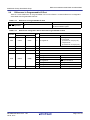
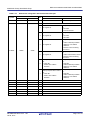
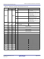
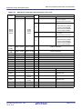
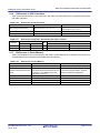
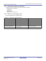
APPLICATION NOTE
M16C/62P Group, M16C/65C Group
Differences between M16C/62P and M16C/65C
R01AN0443EJ0100
Rev. 1.00
Jul 29, 2011
Abstract
The following document describes differences between M16C/62P 100-pin version and M16C/65C 100-pin
version. Refer to each device's hardware manual for details.
Products
MCUs: M16C/62P Group, M16C/65C Group
With its enhanced peripheral functions, the M16C/65C Group MCU has pin assignments and peripheral
functions that are compatible with the M16C/62P Group, making it simple to replace the M16C/62P Group
with the M16C/65C Group.
R01AN0443EJ0100 Rev. 1.00
Jul 29, 2011
Page 1 of 31
M16C/62P Group, M16C/65C Group
Differences between M16C/62P and M16C/65C
Contents
1.
Differences ................................................................................................................. 3
1.1
Differences in Functions ................................................................................................................. 3
1.2
Pin Characteristics .......................................................................................................................... 6
2.
Detailed Comparison ................................................................................................. 7
2.1
Differences in Protection ................................................................................................................. 7
2.2
Differences in Reset ....................................................................................................................... 7
2.3
Differences in Voltage Detector ...................................................................................................... 8
2.4
Differences in Clock Generator ....................................................................................................... 9
2.5
Differences in Power Control ........................................................................................................ 10
2.6
Differences in Processor Mode ..................................................................................................... 10
2.7
Differences in Bus ..........................................................................................................................11
2.8
Differences in Programmable I/O Port .......................................................................................... 12
2.9
Differences in Interrupts ................................................................................................................ 13
2.10
Differences in Watchdog Timer ..................................................................................................... 16
2.11
Differences in DMAC .................................................................................................................... 17
2.12
Differences in Timers .................................................................................................................... 19
2.13
Differences in the Three-phase Motor Control Timer Function ..................................................... 22
2.14
Differences in Serial Interface ....................................................................................................... 23
2.15
Differences in A/D Converter ........................................................................................................ 26
2.16
Differences in CRC Calculator ...................................................................................................... 27
2.17
Differences in Flash Memory ........................................................................................................ 27
2.18
Differences in Flash Memory Block Configuration ........................................................................ 29
2.19
New Functions added in the M16C/65C ....................................................................................... 30
2.20
Differences in Development Tool .................................................................................................. 30
3.
Reference Documents ............................................................................................. 31
R01AN0443EJ0100 Rev. 1.00
Jul 29, 2011
Page 2 of 31
Differences between M16C/62P and M16C/65C
M16C/62P Group, M16C/65C Group
1.
Differences
1.1
Differences in Functions
Table 1.1 and Table 1.3 list Differences in Functions.
Differences in Functions (1/3) (1)
Table 1.1
Item
M16C/62P
M16C/65C
Minimum Instruction
Execution Time
41.7 ns (f(BCLK) = 24 MHz, VCC1 = 3.0 to 5.5
V)
31.25 ns (f(BLCK) = 32 MHz, VCC1 = 2.7 to
100 ns (f(BCLK) = 10 MHz, VCC1 = 2.7 to
5.5 V)
5.5 V)
Clock Generator
PLL, XIN, XCIN, on-chip oscillator (approx.1
MHz)
PLL, XIN, XCIN, 125 kHz on-chip oscillator,
40 MHz on-chip oscillator
Timer/peripheral clock
stop function
No
Yes
Slow read
mode
No
Yes
Low current
consumption No
read mode
Yes
Power
Control
CPU Clock After Reset
NMI Pin
Expanded
area
External
Bus
Main clock divided by 8
125 kHz on-chip oscillator clock divided by 8
NMI interrupt input port
PM24 bit = 0 (when NMI is disabled):
I/O port (N-channel open drain output)
PM24 bit = 1 (when NMI is enabled):
NMI interrupt input port
04000h to 07FFFh (when PM13 = 0)
08000h to 0CFFFh (when PM10 = 0)
04000h to 07FFFh (when PM13 = 0)
0D800h to 0DFFFh
08000h to 0FFFFh (when PM10 = 0)
0E000h to 0FFFFh (when PM10 = 0)
10000h to 26FFFh
10000h to 13FFFh (when PRG2C0 = 1)
28000h to 7FFFFh
14000h to 26FFFh
80000h to CFFFFh (when PM13 = 0)
28000h to 7FFFFh
D0000h to FFFFFh (in microprocessor mode)
80000h to CFFFFh (when PM13 = 0)
D0000h to FFFFFh (in microprocessor mode)
HOLD input
Enabled
Disabled
Bus wait
0 to 3 wait(s) selectable
0 to 8 wait(s) selectable
Recovery
cycle
No
0 to 3 cycle(s) selectable
External interrupts: 8
External interrupts: 13
Interrupt
Reset start
No
Selectable from start and stop
Watchdog function
Timer
Count source CPU clock, on-chip oscillator (approx. 1 MHz) CPU clock, on-chip oscillator (125 kHz)
DMA
DMAC
2 channels
Trigger sources: 25
4 channels
Trigger sources: 43
PM24: Bit in the PM2 register
PM13, PM10: Bits in the PM1 register
PRG2C0: Bit in the PRG2C register
Note:
1.
Refer to the User’s Manual: Hardware for electrical characteristics and more details.
R01AN0443EJ0100 Rev. 1.00
Jul 29, 2011
Page 3 of 31
Differences between M16C/62P and M16C/65C
M16C/62P Group, M16C/65C Group
Table 1.2
Differences in Functions (2/3) (1)
Item
Timer A, timer B
count source
Timer
Serial
Interface
A/D
Converter
CRC
Calculator
M16C/62P
Selectable from f1, f2, f8, f32, and fC32
M16C/65C
Selectable from f1TIMAB and f2TIMAB,
f8TIMAB, f32TIMAB, f64TIMAB, fOCO-S,
fOCO-F, and fC32
Real-time clock
No
Count: second, minute, hour, day of week
PWM function
No
8 bits x 2
Remote control
signal receive
function
No
2 circuits
UART
Clock synchronous/asynchronous x 3
channels
Clock synchronous/asynchronous x 6
channels
UART0 to
UART2, UART5
to UART7 clock
prior to division
select function
f1 only
Selectable from f1 and fOCO-F
CEC
No
Yes
Multi-master I2CNo
bus interface
1 channel
Resolution
8-bit/10-bit (selectable)
10-bit only
Operation clock
φAD
Selectable from f1, f1 divided by 2, f1
divided by 3, f1 divided by 4, f1 divided by
Selectable from fAD, fAD divided by 2, fAD
6, f1 divided by 12, fOCO40M divided by 2,
divided by 3, fAD divided by 4, fAD divided
fOCO40M divided by 3, fOCO40M divided
by 6, and fAD divided by 12
by 4, fOCO40M divided by 6, and
fOCO40M divided by 12
Sample and hold Yes/No (selectable)
Yes
Generator
polynomial
Selectable from
CRC-CCITT (X16 + X12 + X5 + 1) and
CRC-16 (X16 + X15 + X2 + 1)
CRC-CCITT (X16 + X12 + X5 + 1)
MSB/LSB select
No
function
Yes
CRC snoop
Yes
No
Note:
1.
Refer to the User’s Manual: Hardware for electrical characteristics and more details.
R01AN0443EJ0100 Rev. 1.00
Jul 29, 2011
Page 4 of 31
Differences between M16C/62P and M16C/65C
M16C/62P Group, M16C/65C Group
Table 1.3
Differences in Functions (3/3) (1)
Item
M16C/62P
Address FFFFFh
ROM code protect select function
function setting
Flash
Memory
M16C/65C
Selectable Options
• Watchdog timer autostart function (after
reset)
• Count source protection mode select
function (after reset)
• ROM code protect function
• Vdet0 select function
• Voltage monitor 0 reset function (after
hardware reset)
Memory map
User ROM
Program ROM 080000h to 0FFFFFh
Data flash
Block A
00F000h to 00FFFFh
User ROM
• Program ROM 1 080000h to 0FFFFFh
• Program ROM 2 010000h to 013FFFh
Data flash
• Block A
00E000h to 00EFFFh
• Block B
00F000h to 00FFFFh
User ROM
(512-Kbyte)
64 KB x 7
32 KB x 1
8 KB x 3
4 KB x 2
64 KB x 8
16 KB x 1 (program ROM 2)
Data flash
4 KB x 1 (block A)
4 KB x 2 (block A, block B)
Program method In units of 1 word (16-bit)
In units of 2 words (32-bit)
Erase method
Erase all unlocked blocks, block erase
Block erase
User boot mode
No
Yes
Note:
1.
Refer to the User’s Manual: Hardware for electrical characteristics and more details.
R01AN0443EJ0100 Rev. 1.00
Jul 29, 2011
Page 5 of 31
Differences between M16C/62P and M16C/65C
M16C/62P Group, M16C/65C Group
1.2
Pin Characteristics
Table 1.4 lists Differences in Pin Characteristics.
Table 1.4
Differences in Pin Characteristics
M16C/62P
M16C/65C
Changes from M16C/62P
P9_4 / TB4IN / DA1
P9_4 / TB4IN / DA1 / PWM1
Added: PWM1
P9_3 / TB3IN / DA0
P9_3 / TB3IN / DA0 / PWM0
Added: PWM0
P9_2 / TB2IN / SOUT3
P9_2 / TB2IN / SOUT3 / PMC0
Added: PMC0
P9_1 / TB1IN / SIN3
P9_1 / TB1IN / SIN3 / PMC1
Added: PMC1
P8_5 / NMI
P8_5 / NMI / SD / CEC
Added: SD/CEC
P8_1 / TA4IN / U
P8_1 / TA4IN / U / CTS5 / RTS5
Added: CTS5 / RTS5
P8_0 / TA4OUT / U
P8_0 / TA4OUT / U / RXD5 / SCL5
Added: RXD5/SCL5
P7_7 / TA3IN
P7_7 / TA3IN / CLK5
Added: CLK5
P7_6 / TA3OUT
P7_6 / TA3OUT / TXD5 / SDA5
Added: TXD5/SDA5
P7_1 / TA0IN / TB5IN / RXD2 / SCL2
P7_1 / TA0IN / TB5IN / RXD2 / SCL2 / SCLMM Added: SCLMM
P7_0 / TA0OUT / TXD2 / SDA2
P7_0 / TA0OUT / TXD2 / SDA2 / SDAMM
Added: SDAMM
P6_0 / CTS0 / RTS0
P6_0 / CTS0 / RTS0 / RTCOUT
Added: RTCOUT
P4_7 / CS3
P4_7 / CS3 / PWM1 / TXD7 / SDA7
Added: PWM1/TXD7/SDA7
P4_6 / CS2
P4_6 / CS2 / PWM0 / RXD7 / SCL7
Added: PWM0/RXD7/SCL7
P4_5 / CS1
P4_5 / CS1 / CLK7
Added: CLK7
P4_4 / CS0
P4_4 / CS0 / CTS7 / RTS7
Added: CTS7 / RTS7
P2_5 / AN2_5 / A5 (/ D5 / D4)
P2_5 / INT7 / AN2_5 / A5, [A5 / D5], [A5 / D4]
Added: INT7
P2_4 / AN2_4 / A4 (/ D4 / D3)
P2_4 / INT6 / AN2_4 / A4, [A4 / D4], [A4 / D3]
Added: INT6
P1_7 / INT5 / D15
P1_7 / INT5 / D15 / IDU
Added: IDU
P1_6 / INT4 / D14
P1_6 / INT4 / D14 / IDW
Added: IDW
P1_5 / INT3 / D13
P1_5 / INT3 / D13 / IDV
Added: IDV
P1_3 / D11
P1_3 / D11 / TXD6 / SDA6
Added: TXD6 / SDA6
P1_2 / D10
P1_2 / D10 / RXD6 / SCL6
Added: RXD6 / SCL6
P1_1 / D9
P1_1 / D9 / CLK6
Added: CLK6
P1_0 / D8
P1_0 / D8 / CTS6 / RTS6
Added: CTS6 / RTS6
R01AN0443EJ0100 Rev. 1.00
Jul 29, 2011
Page 6 of 31
Differences between M16C/62P and M16C/65C
M16C/62P Group, M16C/65C Group
2.
Detailed Comparison
2.1
Differences in Protection
Table 2.1 lists Differences in Registers Associated with the Protect Function.
Table 2.1
Symbol
Differences in Registers Associated with the Protect Function
Address
M16C/62P
PRCR
2.2
M16C/65C
000Ah
Differences
Bit
000Ah
M16C/62P
M16C/65C
0
Protect bit 0
Enable write access to registers
CM0, CM1, CM2, PLC0, and
PCLKR
Protect bit 0
Enable write access to registers
CM0, CM1, CM2, PLC0,
PCLKR, and FRA0
3
Protect bit 3
Enable write access to registers
VCR2, and D4INT
Protect bit 3
Enable write access to registers
VCR2, VWCE, VD1LS, VW0C,
VW1C, and VW2C
6
—
Protect bit 6
Enable write access to the
PRG2C register
Differences in Reset
Table 2.2 lists Differences in Reset and Table 2.3 lists Difference in the Register Associated with Reset.
Table 2.2
Differences in Reset
Item
M16C/62P
M16C/65C
Types of resets
Hardware reset
Brown-out detection reset
Oscillation stop detection reset
Watchdog timer reset
Software reset
Hardware reset
Voltage monitor 0 reset
Voltage monitor 1 reset
Voltage monitor 2 reset
Power-on reset
Oscillation stop detection reset
Watchdog timer reset
Software reset
Cold start, warm start
discrimination method
WDC5 bit in the WDC register
CWR bit in the RSTFR register
Reset Source
Determine Register
No
Yes
Table 2.3
Symbol
RSTFR
Difference in the Register Associated with Reset
Address
M16C/62P
M16C/65C
—
0018h
R01AN0443EJ0100 Rev. 1.00
Jul 29, 2011
Differences
Bit
—
M16C/62P
—
M16C/65C
M16C/65C only
Page 7 of 31
Differences between M16C/62P and M16C/65C
M16C/62P Group, M16C/65C Group
2.3
Differences in Voltage Detector
Table 2.4 lists Differences in Voltage Detector and Table 2.5 lists Differences in Registers Associated with
Voltage Detector.
Table 2.4
Differences in Voltage Detector
Item
M16C/62P
Voltage detection
interrupt monitor level
M16C/65C
Vdet4
• Vdet1 (voltage detection circuit 1)
• Vdet2 (voltage detection circuit 2)
Voltage detection reset
Vdet3
monitor level
• Vdet0 (voltage detection circuit 0)
• Vdet1 (voltage detection circuit 1)
• Vdet2 (voltage detection circuit 2)
Refer to the Electric Characteristics chapter in the User’s Manual: Hardware for detection voltage.
Table 2.5
Symbol
VCR2
Differences in Registers Associated with Voltage Detector
Address
M16C/62P
001Ah
M16C/65C
001Ah
Differences
Bit
M16C/62P
M16C/65C
5
Reserved bit
Voltage detector 0 enable bit
0: Voltage detector 0 disabled
1: Voltage detector 0 enabled
6
Reset Level Monitor Bit
0 : Disable reset level detection circuit
1 : Enable reset level detection circuit
Voltage detector 1 enable bit
0: Voltage detector 1 disabled
1: Voltage detector 1 enabled
7
Low Voltage Monitor Bit
0 : Disable low voltage detection circuit
1 : Enable low voltage detection circuit
Voltage detector 2 enable bit
0: Voltage detector 2 disabled
1: Voltage detector 2 enabled
D4INT
001Fh
—
—
M16C/62P only
—
VWCE
—
0026h
—
—
M16C/65C only
VD1LS
—
0028h
—
—
M16C/65C only
VW0C
—
002Ah
—
—
M16C/65C only
VW1C
—
002Bh
—
—
M16C/65C only
VW2C
—
002Ch
—
—
M16C/65C only
R01AN0443EJ0100 Rev. 1.00
Jul 29, 2011
Page 8 of 31
Differences between M16C/62P and M16C/65C
M16C/62P Group, M16C/65C Group
2.4
Differences in Clock Generator
Table 2.6 lists Differences in Clock Generator and Table 2.7 and Table 2.8 list Differences in Registers
Associated with Clock Generator (1/2).
Table 2.6
Differences in Clock Generator
Item
M16C/62P
M16C/65C
Clock output function
Selectable from fC, f8, and f32
Selectable from fC, f8, f32, and f1
CPU clock after reset
Main clock divided by 8
(default setting of the CM21 bit: 0)
125 kHz on-chip oscillator clock divided by 8
(default setting of CM21 bit: 1)
Peripheral clock (fC)
Provided constantly
Selectable whether fC is provided or not by
setting the PM25 bit in the PM2 register.
40 MHz on-chip
oscillator
No
Yes
125 kHz on-chip
oscillator
No
Yes
On-chip oscillator
frequency
Approx. 1 MHz
Approx. 125 kHz, approx. 40 MHz
Calculation formula for
PLL clock frequency
f(XIN) x n
f(XIN)/m x n
Timer/peripheral clock
stop function
No
Yes
CM21: Bit in the CM1 register
n: Multiply ratio set by bits PLC02 to PLC00 in the PLC0 register
m: Division ratio set by bits PLC05 to PLC04 in the PLC0 register
Table 2.7
Symbol
Differences in Registers Associated with Clock Generator (1/2)
Address
Bit
M16C/62P M16C/65C
Differences
M16C/62P
3
CM1
0007h
0007h
Reserved bits
4
—
PCLKR
025Eh
0012h
PCLKSTP1
—
0016h
PLC0
001Ch
001Ch
5 Reserved bit
— —
Reserved bit
4
Set to 1.
5 Reserved bit
R01AN0443EJ0100 Rev. 1.00
Jul 29, 2011
M16C/65C
XIN-XOUT feedback resistor select bit
0 : Internal feedback resistor connected
1 : Internal feedback resistor not
connected
125 kHz on-chip oscillator stop bit
0: 125 kHz on-chip oscillator on
1: 125 kHz on-chip oscillator off
Different addresses
Clock output function extension bit
(enabled in single-chip mode)
0: Selected by setting bits CM01 to CM00
in the CM0 register
1: Output f1
M16C/65C only
Reference frequency counter set bit
00: No division
01: Divide-by-2
10: Divide-by-4
11: Do not set
Page 9 of 31
Differences between M16C/62P and M16C/65C
M16C/62P Group, M16C/65C Group
Table 2.8
Differences in Registers Associated with Clock Generator (2/2)
Address
Bit
M16C/62P M16C/65C
Symbol
0
2
PM2
001Eh
001Eh
4
5
FRA0
2.5
—
0022h
—
Differences
M16C/62P
M16C/65C
Specifying wait when accessing
SFR at PLL operation
Reserved bit
0 : 2 waits
Set to 1.
1 : 1 wait
WDT count source protect bit
0: CPU clock is used for the
watchdog timer count source
No register bit
1: On-chip oscillator clock is used
for the watchdog timer count
source
NMI interrupt enable bit
0: NMI interrupt disabled
Reserved bit
1: NMI interrupt enabled
Peripheral clock fC provide bit
No register bit
0: Not provided
1: Provided
—
M16C/65C only
Differences in Power Control
Table 2.9 lists Differences in Power Control and Table 2.10 lists Difference in the Register Associated with
Power Control.
Table 2.9
Differences in Power Control
Item
M16C/62P
M16C/65C
Slow read mode
No
Yes
Low current consumption read mode
No
Yes
Table 2.10
Difference in the Register Associated with Power Control
Address
Symbol
M16C/62P
M16C/65C
—
0222h
FMR2
2.6
Differences
Bit
—
M16C/62P
M16C/65C
—
M16C/65C only
Differences in Processor Mode
Table 2.11 lists Differences in Registers Associated with Processor Mode.
Table 2.11
Symbol
Differences in Registers Associated with Processor Mode
Address
M16C/62P M16C/65C
Differences
Bit
M16C/62P
PM1
0005h
0005h
0
CS2 area switch bit
0: 08000h to 26FFFh
(block A disabled)
1: 10000h to 26FFFh
(block A enabled)
PRG2C
—
0010h
—
—
R01AN0443EJ0100 Rev. 1.00
Jul 29, 2011
M16C/65C
CS2 area switch bit
0: CS2 area (0E000h to 0FFFFh)
1: Data flash (0E000h to 0FFFFh)
M16C/65C only
Page 10 of 31
Differences between M16C/62P and M16C/65C
M16C/62P Group, M16C/65C Group
2.7
Differences in Bus
Table 2.12 lists Differences in Bus and Table 2.13 lists Differences in Registers Associated with Bus.
Table 2.12
Differences in Bus
Item
M16C/62P
M16C/65C
External area wait
Selectable from 0 to 3 wait(s)
CSiW bit in the CSR register,
Selected by bits CSEi0W and CSEi1W in the
CSE register (i = 0 to 3)
Selectable from 0 to 8 wait(s)
Selected by CSiW bit in the CSR register, bits
CSEi0W and CSEi1W in the CSE register, and
bits EWCi0 to EWCi1 in the EWC register
Recovery cycle
No
Selectable from 0 to 3 cycle(s)
Selectable by bits EWR0 to EWR1 in the EWR
register
Table 2.13
Symbol
Differences in Registers Associated with Bus
Address
M16C/62P
M16C/65C
Differences
Bit
M16C/62P
M16C/65C
CS0 wait expansion bit
1-0
CS0 wait expansion bit
b1 b0
b1 b0
1 1: Select wait states by bits
EWC01 and EWC00 in the
EWC register
1 1: Do not set
CS1 wait expansion bit
3 -2
CS1 wait expansion bit
b3 b2
b3 b2
1 1: Select wait states by bits
EWC11 and EWC10 in the
EWC register
1 1: Do not set
CSE
001Bh
001Bh
CS2 wait expansion bit
5-4
CS2 wait expansion bit
b5 b4
b5 b4
1 1: Select wait states by bits
EWC21 and EWC20 in the
EWC register
1 1: Do not set
CS3 wait expansion bit
7-6
CS3 wait expansion bit
b7 b6
b7 b6
1 1: Do not set
1 1: Select wait states by bits
EWC31 and EWC30 in the
EWC register
EWC
—
0011h
—
—
M16C/65C only
EWR
—
0009h
—
—
M16C/65C only
R01AN0443EJ0100 Rev. 1.00
Jul 29, 2011
Page 11 of 31
Differences between M16C/62P and M16C/65C
M16C/62P Group, M16C/65C Group
2.8
Differences in Programmable I/O Port
Table 2.14 lists Difference in Programmable I/O Port and Table 2.15 lists Differences in Registers
Associated with Programmable I/O Port.
Table 2.14
Difference in Programmable I/O Port
Item
M16C/62P
NMI / SD digital filter
Table 2.15
Symbol
M16C/65C
Selectable whether the digital filter is used or
not with the NMIDF register
No
Differences in Registers Associated with Programmable I/O Port
Address
M16C/62P
M16C/65C
Differences
Bit
M16C/62P
Port P8_5 direction bit
0 : Input mode
(Functions as an input port)
1 : Output mode
(Functions as an output port)
PD8
03F2h
03F2h
5
PUR0
03FCh
0360h
—
Different addresses
PUR1
03FDh
0361h
—
Different addresses
PUR2
03FEh
0362h
—
Different addresses
—
Different addresses
PCR
NMIDF
03FFh
—
R01AN0443EJ0100 Rev. 1.00
Jul 29, 2011
0366h
0369h
No register bit
M16C/65C
3
No register bit
Reserved bit
4
No register bit
CEC output enable bit
5
No register bit
INT6 input enable bit
6
No register bit
INT7 input enable bit
7
No register bit
Key input enable bit
—
—
M16C/65C only
Page 12 of 31
Differences between M16C/62P and M16C/65C
M16C/62P Group, M16C/65C Group
2.9
Differences in Interrupts
Table 2.16 lists Difference in Interrupts, and Table 2.17 to Table 2.18 list Differences in Interrupt Vectors,
and Table 2.19 lists Differences in Registers Associated with Interrupts.
Table 2.16
Difference in Interrupts
Item
M16C/62P
NMI enable function
Table 2.17
Software
Interrupt
Number
M16C/65C
Selectable whether to enable or disable the
function with the PM24 bit in the PM2 register
Enable only
Differences in Interrupt Vectors (1/2)
Vector Address
M16C/62P
0
+0 to +3 (0000h to 0003h)
1
+4 to +7 (0004h to 0007h)
2
+8 to +11 (0008h to 000Bh)
3
+12 to +15 (000Ch to 000Fh)
4
+16 to +19 (0010h to 0013h)
INT3
INT3
5
+20 to +23 (0014h to 0017h)
Timer B5
Timer B5
6
+24 to +27 (0018h to 001Bh)
Timer B4, UART1 start/stop
condition detection, bus collision
detection
Timer B4, UART1 start/stop
condition detection, bus collision
detection
7
+28 to +31 (001Ch to 001Fh)
Timer B3, UART0 start/stop
condition detection, bus collision
detection
Timer B3, UART0 start/stop
condition detection, bus collision
detection
8
+32 to +35 (0020h to 0023h)
SI/O4, INT5
SI/O4, INT5
9
+36 to +39 (0024h to 0027h)
SI/O3, INT4
SI/O3, INT4
10
+40 to +43 (0028h to 002Bh)
UART2 start/stop condition
detection, bus collision detection
UART2 start/stop condition
detection, bus collision detection
11
+44 to +47 (002Ch to 002Fh)
DMA0
DMA0
12
+48 to +51 (0030h to 0033h)
DMA1
DMA1
13
+52 to +55 (0034h to 0037h)
Key input interrupt
Key input interrupt
14
+56 to +59 (0038h to 003Bh)
A/D converter
A/D converter
15
+60 to +63 (003Ch to 003Fh)
UART2 transmit, NACK2
UART2 transmit, NACK2
16
+64 to +67 (0040h to 0043h)
UART2 receive, ACK2
UART2 receive, ACK2
17
+68 to +71 (0044h to 0047h)
UART0 transmit, NACK0
UART0 transmit, NACK0
18
+72 to +75 (0048h to 004Bh)
UART0 receive, ACK0
UART0 receive, ACK0
19
+76 to +79 (004Ch to 004Fh)
UART1 transmit, NACK1
UART1 transmit, NACK1
20
+80 to +83 (0050h to 0053h)
UART1 receive, ACK1
UART1 receive, ACK1
21
+84 to +87 (0054h to 0057h)
Timer A0
Timer A0
22
+88 to +91 (0058h to 005Bh)
Timer A1
Timer A1
23
+92 to +95 (005Ch to 005Fh)
Timer A2
Timer A2
24
+96 to +99 (0060h to 0063h)
Timer A3
Timer A3
25
+100 to +103 (0064h to 0067h) Timer A4
Timer A4
26
+104 to +107 (0068h to 006Bh) Timer B0
Timer B0
27
+108 to +111 (006Ch to 006Fh) Timer B1
Timer B1
28
+112 to +115 (0070h to 0073h) Timer B2
Timer B2
R01AN0443EJ0100 Rev. 1.00
Jul 29, 2011
BRK instruction
M16C/65C
BRK instruction
INT instruction interrupt
— (Reserved)
INT7
INT6
Page 13 of 31
Differences between M16C/62P and M16C/65C
M16C/62P Group, M16C/65C Group
Table 2.18
Differences in Interrupt Vectors (2/2)
Software
Interrupt
Number
Vector Address
M16C/62P
29
+116 to +119 (0074h to 0077h)
INT0
INT0
30
+120 to +123 (0078h to 007Bh)
INT1
INT1
31
+124 to +127 (007Ch to 007Fh)
INT2
INT2
32 to 40
+128 to +131 (0080h to 0083h)
to
+160 to +163 (00A0h to 00A3h)
INT instruction interrupt
41
+164 to +167 (00A4h to 00A7h)
DMA2
42
+168 to +171 (00A8h to 00ABh)
DMA3
43
+172 to +175 (00ACh to 00AFh)
UART5 start/stop condition
detection, bus collision detection,
CEC1
44
+176 to +179 (00B0h to 00B3h)
UART5 transmit, NACK5, CEC2
45
+180 to +183 (00B4h to 00B7h)
UART5 receive, ACK5
46
+184 to +187 (00B8h to 00BBh)
UART6 start/stop condition
detection, bus collision detection,
real-time clock period
47
+188 to +191 (00BCh to 00BFh)
UART6 transmit, NACK6,
real-time clock compare
48
+192 to +195 (00C0h to 00C3h)
UART6 receive, ACK6
49
+196 to +199 (00C4h to 00C7h)
UART7 start/stop condition
detection, bus collision detection,
remote control 0
50
+200 to +203 (00C8h to 00CBh)
UART7 transmit, NACK7,
remote control 1
51
+204 to +207 (00CCh to 00CFh)
UART7 receive, ACK7
52 to 58
+208 to +211 (00D0h to 00D3h)
to
+232 to +235 (00E8h to 00EBh)
INT instruction interrupt
59
+236 to +239 (00ECh to 00EFh)
I2C-bus interface interrupt
60
+240 to +243 (00F0h to 00F3h)
SCL/SDA interrupt
61 to 63
+244 to +247 (00F4h to 00F7h)
to
+252 to +255 (00FCh to 00FFh)
INT instruction interrupt
INT instruction interrupt
R01AN0443EJ0100 Rev. 1.00
Jul 29, 2011
M16C/65C
Page 14 of 31
Differences between M16C/62P and M16C/65C
M16C/62P Group, M16C/65C Group
Table 2.19
Symbol
IFSR3A
Differences in Registers Associated with Interrupts
Address
M16C/62P
M16C/65C
—
0205h
—
—
Different addresses
3
4
035Eh
M16C/62P
—
2
IFSR2A
Differences
Bit
M16C/65C
M16C/65C only
No register bit
Interrupt request source select
bit
0: Not used
1: I2C-bus interface
No register bit
Interrupt request source select
bit
0: Not used
1: SCL/SDA
No register bit
Interrupt request source select
bit
0: UART7 start/stop condition
detection, bus collision
detection
1: Remote control receiving
function 0
No register bit
Interrupt request source select
bit
0: UART7 transmission, NACK
1: Remote control receiving
function 1
0206h
5
6
7
Interrupt request factor select
bit
0: Timer B3
1: UART0 bus collision
detection
Interrupt request factor select
bit
0: Timer B4
1: UART1 bus collision
detection
Interrupt request source select
bit
0: Timer B3
1: UART0 start/stop condition
detection, bus collision
detection
Interrupt request source select
bit
0: Timer B4
1: UART1 start/stop condition
detection, bus collision
detection
IFSR
035Fh
0207h
—
Different addresses
AIER
0009h
020Eh
—
Different addresses
AIER2
01BBh
020Fh
—
Different addresses
RMAD0
0010h to 0012h
0210h to 0212h
—
Different addresses
RMAD1
0014h to 0016h
0214h to 0216h
—
Different addresses
RMAD2
01B8h to 01BAh
0218h to 021Ah
—
Different addresses
RMAD3
01BCh to 01BEh 021Ch to 021Eh
—
Different addresses
R01AN0443EJ0100 Rev. 1.00
Jul 29, 2011
Page 15 of 31
Differences between M16C/62P and M16C/65C
M16C/62P Group, M16C/65C Group
2.10
Differences in Watchdog Timer
Table 2.20 lists Differences in Watchdog Timer and Table 2.21 lists Differences in Registers Associated
with Watchdog Timer.
Table 2.20
Differences in Watchdog Timer
Item
M16C/62P
M16C/65C
Count source protect
mode enable setting
Set the PM22 bit in the PM2 register to 1.
Set the CSPRO bit in the CSPR register to 1.(1)
Watchdog timer cycle
in count source
protection mode
Approx. 32.8 ms (32768 / approx. 1 MHz)
Approx. 32.8 ms (4096 / approx. 125 kHz)
Watchdog timer
counter refresh
Write 00h, and then FFh to the WDTR register
Count start conditions
Watchdog timer counter is initialized and starts •Count automatically starts after reset by
counting by writing to the WDTS register.
setting the WDTON bit in the OFS1 address
to 0.
•Count starts by writing to the WDTS register.
Note:
1. When the CSPROINI bit in the OFS1 address is 0, the value after reset becomes 1.
Table 2.21
Symbol
WDTS
Differences in Registers Associated with Watchdog Timer
Address
M16C/62P M16C/65C
000Eh
037Eh
Differences
Bit
M16C/62P
—
M16C/65C
Different addresses
—
Different addresses
5
Cold Start / Warm Start Discrimination Flag
0 : Cold Start
1 : Warm Start
No register bit
WDC
000Fh
037Fh
VW2C
—
002Ch
—
—
M16C/65C only
CSPR
—
037Ch
—
—
M16C/65C only
WDTR
—
037Dh
—
—
M16C/65C only
R01AN0443EJ0100 Rev. 1.00
Jul 29, 2011
Page 16 of 31
Differences between M16C/62P and M16C/65C
M16C/62P Group, M16C/65C Group
2.11
Differences in DMAC
Table 2.22 lists Difference in DMAC, Table 2.23 to Table 2.24 list Differences in DMA Request Sources,
and Table 2.25 lists Differences in Registers Associated with DMAC.
Table 2.22
Difference in DMAC
Item
M16C/62P
Number of channels
Table 2.23
M16C/65C
4 channels
Differences in DMAi Request Sources (i = 0 and 1 in M16C/62P; i = 0 to 3 in M16C/65C) (1/2)
M16C/62P
DSEL4 to
DSEL0
00000b
2 channels
DMS = 0
M16C/65C
DMS = 1
DMS = 0
DMS = 1
Falling edge of INTi pin
—
Falling edge of INTi pin
00001b
Software trigger
—
Software trigger
—
00010b
Timer A0
—
Timer A0
—
—
00011b
Timer A1
—
Timer A1
—
00100b
Timer A2
—
Timer A2
—
00101b
Timer A3
SI/O3 (DMA1 only)
Timer A3
SI/O3 (DMA1, DMA3
only)
Timer A4
DMA0:
Both edges of INTi pin
Timer A4
DMA1:
SI/O4
DMA0, DMA2:
Both edges of INTi pin
DMA1, DMA3:
SI/O4
00111b
Timer B0
DMA0, DMA2:
Timer B3
Timer B0
DMA1, DMA3:
Both edges of INTi pin
DMA0, DMA2:
Timer B3
DMA1,DMA3:
Both edges of INTi pin
01000b
Timer B1
Timer B4 (DMA0 only)
Timer B1
Timer B4 (DMA0,
DMA2 only)
01001b
Timer B2
Timer B5 (DMA0 only)
Timer B2
Timer B5 (DMA0,
DMA2 only)
01010b
UART0 transmission
—
UART0 transmission
—
01011b
DMA0:
UART0 reception
DMA1:
UART0 reception / ACK0
—
DMA0, DMA2:
UART0 reception
DMA1, DMA3:
UART0 reception / ACK0
—
01100b
UART2 transmission
—
UART2 transmission
—
01101b
DMA0:
UART2 reception
DMA1:
UART2 reception / ACK2
—
DMA0, DMA2:
UART2 reception
DMA1, DMA3:
UART2 reception / ACK2
—
01110b
A/D converter
—
A/D converter
—
01111b
DMA0:
UART1 transmission
DMA1:
UART1 reception / ACK1
—
DMA0, DMA2:
UART1 transmission
DMA1, DMA3:
UART1 reception / ACK1
—
00110b
R01AN0443EJ0100 Rev. 1.00
Jul 29, 2011
Page 17 of 31
Differences between M16C/62P and M16C/65C
M16C/62P Group, M16C/65C Group
Table 2.24
DSEL4 to
DSEL0
Differences in DMAi Request Sources (i = 0 and 1 in M16C/62P; i = 0 to 3 in M16C/65C) (2/2)
M16C/62P
DMS = 0
M16C/65C
DMS = 1
DMS = 0
DMS = 1
DMA0, DMA2: UART1 reception
DMA1, DMA3: UART1 transmission
Falling edge of INTj pin (j = 4 to 7)
10001b
UART5 transmission
Both edges of INTj pin
10010b
DMA0, DMA2: UART5 reception
—
DMA1, DMA3: UART5 reception / ACK5
10000b
10011b
UART6 transmission
10100b
DMA0, DMA2: UART6 reception
—
DMA1, DMA3: UART6 reception / ACK6
10101b
UART7 transmission
10110b
DMA0, DMA2: UART7 reception
—
DMA1, DMA3: UART7 reception / ACK7
Table 2.25
Symbol
—
—
Differences in Registers Associated with DMAC
Address
Differences
Bits
M16C/62P
M16C/65C
M16C/62P
M16C/65C
DAR0
0024h to 0026h
0184h to 0186h
—
Different addresses
DAR1
0034h to 0036h
0194h to 0196h
—
Different addresses
DAR2
—
01A4h to 01A6h
—
—
M16C/65C only
DAR3
—
01B4h to 01B6h
—
—
M16C/65C only
DM0CON
002Ch
018Ch
—
Different addresses
DM1CON
003Ch
019Ch
—
Different addresses
DM2CON
—
01ACh
—
—
M16C/65C only
DM3CON
—
01BCh
—
—
M16C/65C only
SAR0
0020h to 0022h
0180h to 0182h
—
Different addresses
SAR1
0030h to 0032h
0190h to 0192h
—
Different addresses
SAR2
—
01A0h to 01A2h
—
—
M16C/65C only
SAR3
—
01B0h to 01B2h
—
—
M16C/65C only
TCR0
0028h to 0029h
0188h to 0189h
—
Different addresses
TCR1
0038h to 0039h
0198h to 0199h
—
Different addresses
TCR2
—
01A8h to 01A9h
—
—
M16C/65C only
TCR3
—
01B8h to 01B9h
—
—
M16C/65C only
DM0SL
03B8h
0398h
—
Different addresses
DM1SL
03BAh
039Ah
—
Different addresses
DM2SL
—
0390h
—
—
M16C/65C only
DM3SL
—
0392h
—
—
M16C/65C only
R01AN0443EJ0100 Rev. 1.00
Jul 29, 2011
Page 18 of 31
Differences between M16C/62P and M16C/65C
M16C/62P Group, M16C/65C Group
2.12
Differences in Timers
Table 2.26 lists Differences in Timers, and Table 2.27 to Table 2.28 list Differences in Registers
Associated with Timers.
Table 2.26
Differences in Timers
Item
M16C/62P
M16C/65C
Count source
f1, f2, f8, f32, fC32
f1TIMAB, f2TIMAB, f8TIMAB, f32TIMAB,
f64TIMAB, fOCO-S, fOCO-F, fC32
Timer clock source
selection
No (always f1)
f1, selectable from main clock
Timer peripheral clock
stop function
No
Yes
Clock select prior to
timer AB division
No
Selectable from f1 and fOCO-F
Output polarity
inversion function
No
Yes
Programmable output
mode
No
Yes
Count direction
(up/down) selected by
the TAiOUT pin
(i = 0 to 4)
Yes
No
Default value in pulse
period/pulse width
measurement modes
Undefined
Programmable
When bits PPWFSk2 to PPWFSk0 in the
PPWFSk register (k = 1 and 2) are 0:
• Contents of the reload register
(measurement result) can be read by reading
the TBj register.
Read from timer
register in pulse
period/pulse width
measurement modes
Contents of the reload register (measurement
When bits PPWFSk2 to PPWFSk0 in the
result) can be read by reading the TBj register
PPWFSk register are 1:
(j = 0 to 5).
• Contents of the counter (current counter
value) can be read by reading the TBj
register
• Contents of the reload register
(measurement result) can be read by reading
the TBj1 register
Write to timer register
in pulse period/pulse
width measurement
modes
The value written to the TBj register is not
written to neither the reload register nor the
counter.
Overflow flag clear
method
Wait one or more count source cycles after the
MR3 bit becomes 1 (overflow) while the TBjS
Write a value to the TBjMR register
bit is 1 (start counting), then write a value to
the TBjMR register.
R01AN0443EJ0100 Rev. 1.00
Jul 29, 2011
When a value is written to the TBj register
while the counter stops, the value is written to
both the reload register and the counter.
Page 19 of 31
Differences between M16C/62P and M16C/65C
M16C/62P Group, M16C/65C Group
Table 2.27
Symbol
Differences in Registers Associated with Timers (1/2)
Address
M16C/62P M16C/65C
Differences
Bits
M16C/62P
2-0 —
—
TAi count source select bit
(i = 0, 2, and 4)
Select the TAi count source
—
TAi count source option specify bit
0: TCK0 and TCK1 enabled, TCS0 to
TCS2 disabled
1: TCK0 and TCK1 disabled, TCS0
to TCS2 enabled
6-4 —
TAj count source select bit (j = 1 and 3)
Select the TAj count source
3
TACS0 to
TACS2
M16C/65C
01D0h to
01D2h
7
—
—
TAj count source option specify bit
0: TCK0 and TCK1 enabled, TCS4 to
TCS6 disabled
1: TCK0 and TCK1 disabled, TCS4
to TCS6 enabled
Different addresses
TA0MR
to
TA4MR
0396h to
039Ah
0336h to
033Ah
TA0
0386h to
0387h
0326h to
0327h
—
Different addresses
TA1
0388h to
0389h
0328h to
0329h
—
Different addresses
TA2
038Ah to
038Bh
032Ah to
032Bh
—
Different addresses
TA3
038Ch to
038Dh
032Ch to
032Dh
—
Different addresses
TA4
038Eh to
038Fh
032Eh to
032Fh
—
Different addresses
TABSR
0380h
0320h
—
Different addresses
UDF
0384h
0324h
—
Different addresses
4
Up/Down switching factor select bit
0: UDF register
—
1: Input signal to TAiOUT pin
ONSF
0382h
0322h
—
Different addresses
TRGSR
0383h
0323h
—
Different addresses
CPSRF
0381h
0015h
—
PCLKSTP1
—
0016h
—
—
M16C/65C only
TCKDIVC0
—
01CBh
—
—
M16C/65C only
PWMFS
—
01D4h
—
—
M16C/65C only
TAPOFS
—
01D5h
—
—
M16C/65C only
TAOW
—
01D8h
—
—
M16C/65C only
TA11
0342h to
0343h
0302h to
0303h
—
TA21
0344h to
0345h
0304h to
0305h
—
TA41
0346h to
0347h
0306h to
0307h
—
R01AN0443EJ0100 Rev. 1.00
Jul 29, 2011
—
—
—
Different addresses
Different addresses
—
Used in programmable output mode
Different addresses
—
Used in programmable output mode
Different addresses
—
Used in programmable output mode
Page 20 of 31
Differences between M16C/62P and M16C/65C
M16C/62P Group, M16C/65C Group
Table 2.28
Symbol
Differences in Registers Associated with Timers (2/2)
Address
M16C/62P
M16C/65C
Differences
Bit
M16C/62P
2-0 —
3
TBCS0
TBCS1
TBCS2
TBCS3
01C8h
01C9h
01E8h
01E9h
—
—
6-4 —
7
—
M16C/65C
TBi count source select bit
(i = 0, 2, 3, and 5)
Select the TBi count source
TBi count source option specify
bit
0: TCK0 and TCK1 enabled,
TCS0 to TCS2 disabled
1: TCK0 and TCK1 disabled,
TCS0 to TCS2 enabled
TBj count source select bit
(j = 1 and 4)
Select the TBj count source
TBj count source option specify
bit
0: TCK0 and TCK1 enabled,
TCS4 to TCS6 disabled
1: TCK0 and TCK1 disabled,
TCS4 to TCS6 enabled
TB0MR
to
TB2MR
039Bh to 039Dh 033Bh to 033Dh
—
Different addresses
TB3MR
to
TB5MR
035Bh to 035Dh 031Bh to 031Dh
—
Different addresses
TB0
0390h to 0391h 0330h to 0331h
—
Different addresses
TB1
0392h to 0393h 0332h to 0333h
—
Different addresses
TB2
0394h to 0395h 0334h to 0335h
—
Different addresses
TB3
0350h to 0351h 0310h to 0311h
—
Different addresses
TB4
0352h to 0353h 0312h to 0313h
—
Different addresses
TB5
0354h to 0355h 0314h to 0315h
TBSR
0340h
0300h
—
Different addresses
—
Different addresses
TABSR
0380h
0320h
—
PPWFS1
—
01C6h
—
—
Different addresses
M16C/65C only
PPWFS2
—
01E6h
—
—
M16C/65C only
TB01
—
01C0h to
01C1h
—
—
M16C/65C only
TB11
—
01C2h to
01C3h
—
—
M16C/65C only
TB21
—
01C4h to
01C5h
—
—
M16C/65C only
TB31
—
01E0h to 01E1h
—
—
M16C/65C only
TB41
—
01E2h to 01E3h
—
—
M16C/65C only
TB51
—
01E4h to 01E5h
—
—
M16C/65C only
R01AN0443EJ0100 Rev. 1.00
Jul 29, 2011
Page 21 of 31
Differences between M16C/62P and M16C/65C
M16C/62P Group, M16C/65C Group
2.13
Differences in the Three-phase Motor Control Timer Function
Table 2.29 lists Differences in the Three-phase Motor Control Timer Function and Table 2.30 lists
Differences in Registers Associated with the Three-phase Motor Control Timer Function.
Table 2.29
Differences in the Three-phase Motor Control Timer Function
Item
M16C/62P
M16C/65C
Count source
f1, f2, f8, f32, fC32
f1TIMAB, f2TIMAB, f8TIMAB, f32TIMAB,
f64TIMAB, fOCO-S, fOCO-F, fC32
Position data retain function
No
Yes
Three-phase PWM output pin
select function
No
Yes
Table 2.30
Symbol
Differences in Registers Associated with the Three-phase Motor Control Timer Function
Address
Differences
Bit
M16C/62P
M16C/65C
DTT
034Ch
030Ch
ICTB2
034Dh
030Dh
—
Different addresses
IDB0
034Ah
030Ah
—
Different addresses
IDB1
034Bh
030Bh
—
Different addresses
INVC0
0348h
0308h
—
Different addresses
0349h
0309h
INVC1
M16C/62P
—
M16C/65C
Different addresses
—
Different addresses
TA1
0388h to 0389h 0328h to 0329h
—
Different addresses
TA2
038Ah to 038Bh 032Ah to 032Bh
—
Different addresses
TA4
038Eh to 038Fh 032Eh to 032Fh
—
Different addresses
TA11
0342h to 0343h 0302h to 0303h
—
Different addresses
TA21
0344h to 0345h 0304h to 0305h
—
Different addresses
TA41
0346h to 0347h 0306h to 0307h
—
Different addresses
—
Different addresses
TB2SC
TB2
039Eh
033Eh
0394h to 0395h 0334h to 0335h
—
Different addresses
Different addresses
0383h
TABSR
0380h
0320h
—
PDRF
—
030Eh
—
PFCR
—
0318h
—
—
M16C/65C only
TPRC
—
01DAh
—
—
M16C/65C only
R01AN0443EJ0100 Rev. 1.00
Jul 29, 2011
0323h
—
TRGSR
Different addresses
—
M16C/65C only
Page 22 of 31
Differences between M16C/62P and M16C/65C
M16C/62P Group, M16C/65C Group
2.14
Differences in Serial Interface
Table 2.31 lists Differences in Serial Interface, and Table 2.32 to Table 2.33 list Differences in Registers
Associated with Serial Interface.
Table 2.31
Differences in Serial Interface
Item
M16C/62P
M16C/65C
Clock synchronous/asynchronous
I2C mode
Special mode 2
3 channels (UART0 to UART2)
6 channels (UART0 to 2, UART5 to 7)
f1 only
Selectable from f1 and fOCO-F
IE mode
Clock selection for UART0 to 2, and
UART5 to 7 prior to division
SI/O3,4
Output control after
transmission
The state after transmission can be
The state of pins SOUT3 and SOUT4 is selected whether to set high-impedance
high-impedance after transmission.
or retain the last bit level with bits SM27
and SM26 in the S34C2 register.
SI/O clock prior to division
f1 only
R01AN0443EJ0100 Rev. 1.00
Jul 29, 2011
Selectable from f1 and fOCO-F
Page 23 of 31
Differences between M16C/62P and M16C/65C
M16C/62P Group, M16C/65C Group
Table 2.32
Symbol
Differences in Registers Associated with Serial Interface (1/2)
Address
Bit
Differences
M16C/62P
M16C/65C
PCLKSTP1
—
0016h
—
U0BRG
03A1h
0249h
—
Different addresses
U0C0
03A4h
024Ch
—
Different addresses
U0C1
03A5h
024Dh
—
Different addresses
03A0h
0248h
—
Different addresses
—
Different addresses
U0MR
U0RB
03A6h to 03A7h 024Eh to 024Fh
U0SMR
036Fh
0247h
U0SMR2
036Eh
0246h
M16C/62P
—
M16C/65C only
—
3
M16C/65C
Different addresses
LSYN
(1)
—
Reserved bit
Different addresses
U0SMR3
036Dh
0245h
—
Different addresses
U0SMR4
036Ch
0244h
—
Different addresses
U0TB
UCON
03A2h to 03A3h 024Ah to 024Bh
03B0h
0250h
—
Different addresses
—
Different addresses
UCLKSEL0
—
0252h
—
U1BRG
03A9h
0259h
—
—
Different addresses
M16C/65C only
U1C0
03ACh
025Ch
—
Different addresses
U1C1
03ADh
025Dh
—
Different addresses
U1MR
03A8h
0258h
—
Different addresses
U1RB
03AEh to
03AFh
025Eh to 025Fh
—
Different addresses
U1SMR
0373h
0257h
U1SMR2
0372h
0256h
—
Different addresses
U1SMR3
0371h
0255h
—
Different addresses
U1SMR4
0370h
0254h
—
Different addresses
U1TB
03AAh to
03ABh
025Ah to 025Bh
—
Different addresses
—
3
Different addresses
LSYN
(1)
Reserved bit
U2BRG
0379h
0269h
—
Different addresses
U2C0
037Ch
026Ch
—
Different addresses
U2C1
037Dh
026Dh
—
Different addresses
U2MR
0378h
0268h
—
Different addresses
U2RB
037Eh to 037Fh 026Eh to 026Fh
—
Different addresses
—
Different addresses
U2SMR
0377h
0267h
U2SMR2
0376h
0266h
—
Different addresses
U2SMR3
0375h
0265h
—
Different addresses
0374h
0264h
U2SMR4
U2TB
037Ah to 037Bh 026Ah to 026Bh
3
LSYN (1)
Reserved bit
—
Different addresses
—
Different addresses
Note:
1. Only enabled in M3062LFGPFP and M3062LFGPGP. This is a reserved bit in other products.
R01AN0443EJ0100 Rev. 1.00
Jul 29, 2011
Page 24 of 31
Differences between M16C/62P and M16C/65C
M16C/62P Group, M16C/65C Group
Table 2.33
Symbol
U5BRG
Differences in Registers Associated with Serial Interface (2/2)
Address
M16C/62P
M16C/65C
—
0289h
Bit
—
Differences
M16C/62P
M16C/65C
—
M16C/65C only
U5C0
—
028Ch
—
—
M16C/65C only
U5C1
—
028Dh
—
—
M16C/65C only
U5MR
—
0288h
—
—
M16C/65C only
U5RB
—
028Eh to 028Fh
—
—
M16C/65C only
U5SMR
—
0287h
—
—
M16C/65C only
U5SMR2
—
0286h
—
—
M16C/65C only
U5SMR3
—
0285h
—
—
M16C/65C only
U5SMR4
—
0284h
—
—
M16C/65C only
U5TB
—
028Ah to 028Bh
—
—
M16C/65C only
U6BRG
—
0299h
—
—
M16C/65C only
U6C0
—
029Ch
—
—
M16C/65C only
U6C1
—
029Dh
—
—
M16C/65C only
U6MR
—
0298h
—
—
M16C/65C only
U6RB
—
029Eh to 029Fh
—
—
M16C/65C only
U6SMR
—
0297h
—
—
M16C/65C only
U6SMR2
—
0296h
—
—
M16C/65C only
U6SMR3
—
0295h
—
—
M16C/65C only
U6SMR4
—
0294h
—
—
M16C/65C only
U6TB
—
029Ah to 029Bh
—
—
M16C/65C only
U7BRG
—
02A9h
—
—
M16C/65C only
U7C0
—
02ACh
—
—
M16C/65C only
U7C1
—
02ADh
—
—
M16C/65C only
U7MR
—
02A8h
—
—
M16C/65C only
U7RB
—
02AEh to 02AFh
—
—
M16C/65C only
U7SMR
—
02A7h
—
—
M16C/65C only
U7SMR2
—
02A6h
—
—
M16C/65C only
U7SMR3
—
02A5h
—
—
M16C/65C only
U7SMR4
—
02A4h
—
—
M16C/65C only
U7TB
—
02AAh to 02ABh
—
—
S3C
0362h
0272h
—
M16C/65C only
Different addresses
S4C
0366h
0276h
—
Different addresses
S3BRG
0363h
0273h
—
Different addresses
S4BRG
0367h
0277h
—
Different addresses
S3TRR
0360h
0270h
—
Different addresses
S4TRR
0364h
0274h
—
S34C2
—
0278h
—
R01AN0443EJ0100 Rev. 1.00
Jul 29, 2011
Different addresses
—
M16C/65C only
Page 25 of 31
Differences between M16C/62P and M16C/65C
M16C/62P Group, M16C/65C Group
2.15
Differences in A/D Converter
Table 2.34 lists Differences in A/D Converters and Table 2.35 lists Differences in Registers Associated
with A/D Converter.
Table 2.34
Differences in A/D Converters
Item
M16C/62P
M16C/65C
Operation clock φAD
f1, f1 divided by 2, f1 divided by 3, f1
divided by 4, f1 divided by 6, f1 divided
fAD, fAD divided by 2, fAD divided by 3,
by 12, fOCO40M divided by 2,
fAD divided by 4, fAD divided by 6, and
fOCO40M divided by 3, fOCO40M
fAD divided by 12
divided by 4, fOCO40M divided by 6,
and fOCO40M divided by 12
Conversion rate per pin
Without sample and hold
8-bit resolution: 49 φAD cycles
10-bit resolution: 59 φAD cycles
With sample and hold
8-bit resolution: 28 φAD cycles
10-bit resolution: 33 φAD cycles
External op-amp connection mode
Yes
No
Resolution
8-bit/10-bit (selectable)
10-bit
Sample and hold
Yes/No (selectable)
Yes
fAD
f1 only
Selectable from f1 and fOCO40M
Minimum 43 φAD cycles
Open-circuit detection assist function No
Table 2.35
Symbol
PCLKSTP1
ADCON1
ADCON2
AINRST
Yes
Differences in Registers Associated with A/D Converter
Address
M16C/62P M16C/65C
—
03D7h
03D4h
—
0016h
03D7h
R01AN0443EJ0100 Rev. 1.00
Jul 29, 2011
M16C/62P
M16C/65C
—
—
M16C/65C only
3
8/10-Bit Mode Select Bit
0: 8-bit mode
1: 10-bit mode
No register bit
5
Vref Connect Bit
0: Vref not connected
1: Vref connected
A/D standby bit
0: A/D operation stopped (standby)
1: A/D operation enabled
External Op-Amp Connection
Mode Bit
0 0: ANEX0 and ANEX1 are not used
7-6 0 1: ANEX0 input is A/D converted
1 0: ANEX1 input is A/D converted
1 1: External op-amp connection
mode
Extended pin select bit
0 0: ANEX0 and ANEX1 are not used
0 1: ANEX0 input is A/D converted
1 0: ANEX1 input is A/D converted
1 1: Do not set
0
A/D Conversion Method Select Bit
0: Without sample and hold function
1: With sample and hold function
No register bit
7
No register bit
fAD select bit
0: f1
1: fOCO40M
—
—
M16C/65C only
03D4h
03A2h
Differences
Bit
Page 26 of 31
Differences between M16C/62P and M16C/65C
M16C/62P Group, M16C/65C Group
2.16
Differences in CRC Calculator
Table 2.36 lists Differences in CRC Calculator and Table 2.37 lists Differences in Registers Associated
with CRC Calculator.
Table 2.36
Differences in CRC Calculator
Item
M16C/62P
M16C/65C
(X16 + X12 + X5 + 1)
CRC generator polynomial
CRC-CCITT (X16 + X12 + X5 + 1)
CRC-CCITT
CRC-16 (X16 + X15 + X2 + 1)
MSB/LSB selection
No
MSB/LSB (selectable)
CRC snoop
No
Yes
Table 2.37
Differences in Registers Associated with CRC Calculator
Address
Symbol
M16C/62P
Differences
Bit
M16C/65C
M16C/62P
M16C/65C
CRCMR
—
03B6h
—
—
M16C/65C only
CRCSAR
—
03B4h to 03B5h
—
—
M16C/65C only
2.17
or
Differences in Flash Memory
Table 2.38 lists Differences in Flash Memory and Table 2.39 lists Differences in Software Commands, and
2.40 lists Differences in Registers Associated with Flash Memory.
Table 2.38
Differences in Flash Memory
Item
Program method
M16C/62P
1-word units (16-bit)
M16C/65C
2-word units (32-bit)
100 times (all areas) or
Number of programs and erase 1,000 times (all blocks other than block A
cycles
and block 1 in user ROM area)/10,000
times (block A, block 1)
1,000 times (program ROM 1, program
ROM 2)/10,000 times (data flash)
Suspend function
No
Yes
User boot function
No
Yes
Forced erase function
No
Yes
Data retention
10 years
20 years
R01AN0443EJ0100 Rev. 1.00
Jul 29, 2011
Page 27 of 31
Differences between M16C/62P and M16C/65C
M16C/62P Group, M16C/65C Group
Table 2.39
Differences in Software Commands
Software
Command
MCU
Program
Erase all unlocked
blocks
Block blank check (1)
First Bus Cycle
Second Bus Cycle
Third Bus Cycle
Address
Data
Address
Data
Address
Data
M16C/62P
WA
XX40h
WA
WD
—
—
M16C/65C
WA
XX41h
WA
WD0
WA
WD1
M16C/62P
X
XXA7h
X
XXD0h
—
—
M16C/65C
—
—
—
—
—
—
M16C/62P
—
—
—
—
—
—
M16C/65C
X
XX25h
BA
XXD0h
—
—
Notes:
1. Block blank check command is designed for programmer manufacturer. Not for customers in general.
WA: Write address (set an even number, however, for M16C/65C, set the end of the address to 0h, 4h,
8h, or Ch only.)
WD: Write data (16 bits)
WD0: Write data lower word (16 bits)
WD1: Write data upper word (16 bits)
BA: Highest block address (even address)
X: Any even address in user ROM area
XX: 8 upper bits of command code (ignored)
Table 2.40
Symbol
Differences in Registers Associated with Flash Memory
Address
M16C/62P
M16C/65C
FIDR
01B4h
—
—
FMR0
01B7h
0220h
—
FMR1
01B5h
Differences
Bit
M16C/62P
M16C/62P only
M16C/65C
—
Different addresses
1
EW1 mode select bit
0: EW0 mode
1: EW1 mode
Write to FMR6 register enable bit
0: Disabled
1: Enabled
7
Reserved bit
Data flash wait bit
0: 1 wait
1: Follow the setting of the PM17 bit
0221h
FMR2
—
0222h
—
—
M16C/65C only
FMR3
—
0223h
—
—
M16C/65C only
FMR6
—
0230h
—
—
M16C/65C only
R01AN0443EJ0100 Rev. 1.00
Jul 29, 2011
Page 28 of 31
Differences between M16C/62P and M16C/65C
M16C/62P Group, M16C/65C Group
2.18
Differences in Flash Memory Block Configuration
The flash ROM block configurations differ between the M16C/62P and the M16C/65C. Figure 2.1 shows
the Differences in Flash Memory Block Configuration. The differences are marked in yellow.
00F000h
00FFFFh
00E000h
Block A: 4 Kbytes
00EFFFh
00F000h
Block A: 4 Kbytes
Block B: 4 Kbytes
00FFFFh
010000h
Program ROM 2:
16 Kbytes
013FFFh
080000h
08FFFFh
090000h
09FFFFh
0A0000h
0AFFFFh
0B0000h
0BFFFFh
0C0000h
0CFFFFh
0D0000h
0DFFFFh
0E0000h
0EFFFFh
0F0000h
0F0000h
Block 12: 64 Kbytes
Block 5: 32 Kbytes
Block 11: 64 Kbytes
Block 10: 64 Kbytes
Block 9: 64 Kbytes
Block 8: 64 Kbytes
Block 7: 64 Kbytes
Block 6: 64 Kbytes
Block 0 to 5
(32+8+8+8+4+4) Kbytes
0FFFFFh
0F7FFFh
0F8000h
09FFFFh
0A0000h
Block 4: 8 Kbytes
0AFFFFh
0B0000h
Block 3: 8 Kbytes
0BFFFFh
0C0000h
0F9FFFh
0FA000h
0FBFFFh
0FC000h
Block 2: 8 Kbytes
0FDFFFh
0FE000h
0FEFFFh
0FF000h
Block 1: 4 Kbytes
Block 0: 4 Kbytes
0FFFFFh
M16C/62P Group
Figure 2.1
080000h
08FFFFh
090000h
0CFFFFh
0D0000h
0DFFFFh
0E0000h
0EFFFFh
0F0000h
0FFFFFh
Block 7: 64 Kbytes
Block 6: 64 Kbytes
Block 5: 64 Kbytes
Block 4: 64 Kbytes
Block 3: 64 Kbytes
Block 2: 64 Kbytes
Block 1: 64 Kbytes
Block 0: 64 Kbytes
M16C/65C Group
Differences in Flash Memory Block Configuration
R01AN0443EJ0100 Rev. 1.00
Jul 29, 2011
Page 29 of 31
Differences between M16C/62P and M16C/65C
M16C/62P Group, M16C/65C Group
2.19
New Functions added in the M16C/65C
The following functions have been added in the M16C/65C Group MCU:
• Multi-master I2C-bus interface
• CEC function
• Real-time clock
• PWM function
• Remote control signal receiver
2.20
Differences in Development Tool
Table 2.41 lists Differences in Development Tool.
Table 2.41
Differences in Development Tool
Tools
M16C/62P
M16C/65C
C compiler
M3T-NC30WA
M3T-NC30WA
Real-time OS
M3T-MR30
M3T-MR30
Emulator debugger
PC7501
E100
Emulation probe
M3062PT2-EPB
—
MCU unit
—
R0E530650MCU00
Compact emulator
M3062PT3-CPE
—
On-chip debugging emulator
E8
E8a (7-wire system)
E8a (single-wire system)
Renesas starter kits
R0K33062PS001BE
—
R01AN0443EJ0100 Rev. 1.00
Jul 29, 2011
Page 30 of 31
M16C/62P Group, M16C/65C Group
3.
Differences between M16C/62P and M16C/65C
Reference Documents
M16C/62P Group Hardware Manual Rev.2.41
M16C/65C Group User’s Manual: Hardware Rev.1.00
The latest version can be downloaded from the Renesas Electronics website.
Technical Update/Technical News
The latest information can be downloaded from the Renesas Electronics website.
Website and Support
Renesas Electronics website
http://www.renesas.com/
Inquiries
http://www.renesas.com/inquiry
R01AN0443EJ0100 Rev. 1.00
Jul 29, 2011
Page 31 of 31
M16C/62P Group, M16C/65C Group
Differences between M16C/62P and M16C/65C
Revision History
Rev.
Date
1.00
Jul 29, 2011
Description
Page
—
Summary
First edition issued
All trademarks and registered trademarks are the property of their respective owners.
A-1
General Precautions in the Handling of MPU/MCU Products
The following usage notes are applicable to all MPU/MCU products from Renesas. For detailed usage notes
on the products covered by this manual, refer to the relevant sections of the manual. If the descriptions under
General Precautions in the Handling of MPU/MCU Products and in the body of the manual differ from each
other, the description in the body of the manual takes precedence.
1. Handling of Unused Pins
Handle unused pins in accord with the directions given under Handling of Unused Pins in the
manual.
 The input pins of CMOS products are generally in the high-impedance state. In operation
with an unused pin in the open-circuit state, extra electromagnetic noise is induced in the
vicinity of LSI, an associated shoot-through current flows internally, and malfunctions occur
due to the false recognition of the pin state as an input signal become possible. Unused
pins should be handled as described under Handling of Unused Pins in the manual.
2. Processing at Power-on
The state of the product is undefined at the moment when power is supplied.
 The states of internal circuits in the LSI are indeterminate and the states of register
settings and pins are undefined at the moment when power is supplied.
In a finished product where the reset signal is applied to the external reset pin, the states
of pins are not guaranteed from the moment when power is supplied until the reset
process is completed.
In a similar way, the states of pins in a product that is reset by an on-chip power-on reset
function are not guaranteed from the moment when power is supplied until the power
reaches the level at which resetting has been specified.
3. Prohibition of Access to Reserved Addresses
Access to reserved addresses is prohibited.
 The reserved addresses are provided for the possible future expansion of functions. Do
not access these addresses; the correct operation of LSI is not guaranteed if they are
accessed.
4. Clock Signals
After applying a reset, only release the reset line after the operating clock signal has become
stable. When switching the clock signal during program execution, wait until the target clock
signal has stabilized.
 When the clock signal is generated with an external resonator (or from an external
oscillator) during a reset, ensure that the reset line is only released after full stabilization of
the clock signal. Moreover, when switching to a clock signal produced with an external
resonator (or by an external oscillator) while program execution is in progress, wait until
the target clock signal is stable.
5. Differences between Products
Before changing from one product to another, i.e. to one with a different part number, confirm
that the change will not lead to problems.
 The characteristics of MPU/MCU in the same group but having different part numbers may
differ because of the differences in internal memory capacity and layout pattern. When
changing to products of different part numbers, implement a system-evaluation test for
each of the products.
Notice
1.
All information included in this document is current as of the date this document is issued. Such information, however, is subject to change without any prior notice. Before purchasing or using any Renesas
Electronics products listed herein, please confirm the latest product information with a Renesas Electronics sales office. Also, please pay regular and careful attention to additional and different information to
be disclosed by Renesas Electronics such as that disclosed through our website.
2.
Renesas Electronics does not assume any liability for infringement of patents, copyrights, or other intellectual property rights of third parties by or arising from the use of Renesas Electronics products or
technical information described in this document. No license, express, implied or otherwise, is granted hereby under any patents, copyrights or other intellectual property rights of Renesas Electronics or
others.
3.
You should not alter, modify, copy, or otherwise misappropriate any Renesas Electronics product, whether in whole or in part.
4.
Descriptions of circuits, software and other related information in this document are provided only to illustrate the operation of semiconductor products and application examples. You are fully responsible for
the incorporation of these circuits, software, and information in the design of your equipment. Renesas Electronics assumes no responsibility for any losses incurred by you or third parties arising from the
use of these circuits, software, or information.
5.
When exporting the products or technology described in this document, you should comply with the applicable export control laws and regulations and follow the procedures required by such laws and
regulations. You should not use Renesas Electronics products or the technology described in this document for any purpose relating to military applications or use by the military, including but not limited to
the development of weapons of mass destruction. Renesas Electronics products and technology may not be used for or incorporated into any products or systems whose manufacture, use, or sale is
prohibited under any applicable domestic or foreign laws or regulations.
6.
Renesas Electronics has used reasonable care in preparing the information included in this document, but Renesas Electronics does not warrant that such information is error free. Renesas Electronics
7.
Renesas Electronics products are classified according to the following three quality grades: "Standard", "High Quality", and "Specific". The recommended applications for each Renesas Electronics product
assumes no liability whatsoever for any damages incurred by you resulting from errors in or omissions from the information included herein.
depends on the product's quality grade, as indicated below. You must check the quality grade of each Renesas Electronics product before using it in a particular application. You may not use any Renesas
Electronics product for any application categorized as "Specific" without the prior written consent of Renesas Electronics. Further, you may not use any Renesas Electronics product for any application for
which it is not intended without the prior written consent of Renesas Electronics. Renesas Electronics shall not be in any way liable for any damages or losses incurred by you or third parties arising from the
use of any Renesas Electronics product for an application categorized as "Specific" or for which the product is not intended where you have failed to obtain the prior written consent of Renesas Electronics.
The quality grade of each Renesas Electronics product is "Standard" unless otherwise expressly specified in a Renesas Electronics data sheets or data books, etc.
"Standard":
Computers; office equipment; communications equipment; test and measurement equipment; audio and visual equipment; home electronic appliances; machine tools;
personal electronic equipment; and industrial robots.
"High Quality": Transportation equipment (automobiles, trains, ships, etc.); traffic control systems; anti-disaster systems; anti-crime systems; safety equipment; and medical equipment not specifically
designed for life support.
"Specific":
Aircraft; aerospace equipment; submersible repeaters; nuclear reactor control systems; medical equipment or systems for life support (e.g. artificial life support devices or systems), surgical
implantations, or healthcare intervention (e.g. excision, etc.), and any other applications or purposes that pose a direct threat to human life.
8.
You should use the Renesas Electronics products described in this document within the range specified by Renesas Electronics, especially with respect to the maximum rating, operating supply voltage
range, movement power voltage range, heat radiation characteristics, installation and other product characteristics. Renesas Electronics shall have no liability for malfunctions or damages arising out of the
use of Renesas Electronics products beyond such specified ranges.
9.
Although Renesas Electronics endeavors to improve the quality and reliability of its products, semiconductor products have specific characteristics such as the occurrence of failure at a certain rate and
malfunctions under certain use conditions. Further, Renesas Electronics products are not subject to radiation resistance design. Please be sure to implement safety measures to guard them against the
possibility of physical injury, and injury or damage caused by fire in the event of the failure of a Renesas Electronics product, such as safety design for hardware and software including but not limited to
redundancy, fire control and malfunction prevention, appropriate treatment for aging degradation or any other appropriate measures. Because the evaluation of microcomputer software alone is very difficult,
please evaluate the safety of the final products or system manufactured by you.
10. Please contact a Renesas Electronics sales office for details as to environmental matters such as the environmental compatibility of each Renesas Electronics product. Please use Renesas Electronics
products in compliance with all applicable laws and regulations that regulate the inclusion or use of controlled substances, including without limitation, the EU RoHS Directive. Renesas Electronics assumes
no liability for damages or losses occurring as a result of your noncompliance with applicable laws and regulations.
11. This document may not be reproduced or duplicated, in any form, in whole or in part, without prior written consent of Renesas Electronics.
12. Please contact a Renesas Electronics sales office if you have any questions regarding the information contained in this document or Renesas Electronics products, or if you have any other inquiries.
(Note 1)
"Renesas Electronics" as used in this document means Renesas Electronics Corporation and also includes its majority-owned subsidiaries.
(Note 2)
"Renesas Electronics product(s)" means any product developed or manufactured by or for Renesas Electronics.
http://www.renesas.com
SALES OFFICES
Refer to "http://www.renesas.com/" for the latest and detailed information.
Renesas Electronics America Inc.
2880 Scott Boulevard Santa Clara, CA 95050-2554, U.S.A.
Tel: +1-408-588-6000, Fax: +1-408-588-6130
Renesas Electronics Canada Limited
1101 Nicholson Road, Newmarket, Ontario L3Y 9C3, Canada
Tel: +1-905-898-5441, Fax: +1-905-898-3220
Renesas Electronics Europe Limited
Dukes Meadow, Millboard Road, Bourne End, Buckinghamshire, SL8 5FH, U.K
Tel: +44-1628-585-100, Fax: +44-1628-585-900
Renesas Electronics Europe GmbH
Arcadiastrasse 10, 40472 Düsseldorf, Germany
Tel: +49-211-65030, Fax: +49-211-6503-1327
Renesas Electronics (China) Co., Ltd.
7th Floor, Quantum Plaza, No.27 ZhiChunLu Haidian District, Beijing 100083, P.R.China
Tel: +86-10-8235-1155, Fax: +86-10-8235-7679
Renesas Electronics (Shanghai) Co., Ltd.
Unit 204, 205, AZIA Center, No.1233 Lujiazui Ring Rd., Pudong District, Shanghai 200120, China
Tel: +86-21-5877-1818, Fax: +86-21-6887-7858 / -7898
Renesas Electronics Hong Kong Limited
Unit 1601-1613, 16/F., Tower 2, Grand Century Place, 193 Prince Edward Road West, Mongkok, Kowloon, Hong Kong
Tel: +852-2886-9318, Fax: +852 2886-9022/9044
Renesas Electronics Taiwan Co., Ltd.
13F, No. 363, Fu Shing North Road, Taipei, Taiwan
Tel: +886-2-8175-9600, Fax: +886 2-8175-9670
Renesas Electronics Singapore Pte. Ltd.
1 harbourFront Avenue, #06-10, keppel Bay Tower, Singapore 098632
Tel: +65-6213-0200, Fax: +65-6278-8001
Renesas Electronics Malaysia Sdn.Bhd.
Unit 906, Block B, Menara Amcorp, Amcorp Trade Centre, No. 18, Jln Persiaran Barat, 46050 Petaling Jaya, Selangor Darul Ehsan, Malaysia
Tel: +60-3-7955-9390, Fax: +60-3-7955-9510
Renesas Electronics Korea Co., Ltd.
11F., Samik Lavied' or Bldg., 720-2 Yeoksam-Dong, Kangnam-Ku, Seoul 135-080, Korea
Tel: +82-2-558-3737, Fax: +82-2-558-5141
© 2011 Renesas Electronics Corporation. All rights reserved.
Colophon 1.1