1
Cover
MICROCOMPUTER
MN101L
MN101LR05D/04D/03D/02D
LSI User’s Manual
Pub.No. 21705-015E
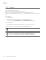
Request for your special attention and precautions in using the technical information and
semiconductors described in this book
(1) If any of the products or technical information described in this book is to be exported or provided to non-residents, the laws and
regulations of the exporting country, especially, those with regard to security export control, must be observed.
(2) The technical information described in this book is intended only to show the main characteristics and application circuit examples
of the products. No license is granted in and to any intellectual property right or other right owned by Panasonic Corporation or any
other company. Therefore, no responsibility is assumed by our company as to the infringement upon any such right owned by any
other company which may arise as a result of the use of technical information described in this book.
(3) The products described in this book are intended to be used for general applications (such as office equipment, communications
equipment, measuring instruments and household appliances), or for specific applications as expressly stated in this book.
Consult our sales staff in advance for information on the following applications:
Special applications (such as for airplanes, aerospace, automotive equipment, traffic signaling equipment, combustion equipment,
life support systems and safety devices) in which exceptional quality and reliability are required, or if the failure or malfunction of
the products may directly jeopardize life or harm the human body.
It is to be understood that our company shall not be held responsible for any damage incurred as a result of or in connection with
your using the products described in this book for any special application, unless our company agrees to your using the products in
this book for any special application.
(4) The products and product specifications described in this book are subject to change without notice for modification and/or improvement. At the final stage of your design, purchasing, or use of the products, therefore, ask for the most up-to-date Product
Standards in advance to make sure that the latest specifications satisfy your requirements.
(5) When designing your equipment, comply with the range of absolute maximum rating and the guaranteed operating conditions
(operating power supply voltage and operating environment etc.). Especially, please be careful not to exceed the range of absolute
maximum rating on the transient state, such as power-on, power-off and mode-switching. Otherwise, we will not be liable for any
defect which may arise later in your equipment.
Even when the products are used within the guaranteed values, take into the consideration of incidence of break down and failure
mode, possible to occur to semiconductor products. Measures on the systems such as redundant design, arresting the spread of fire
or preventing glitch are recommended in order to prevent physical injury, fire, social damages, for example, by using the products.
(6) Comply with the instructions for use in order to prevent breakdown and characteristics change due to external factors (ESD, EOS,
thermal stress and mechanical stress) at the time of handling, mounting or at customer's process. When using products for which
damp-proof packing is required, satisfy the conditions, such as shelf life and the elapsed time since first opening the packages.
(7) This book may be not reprinted or reproduced whether wholly or partially, without the prior written permission of our company.
20100202
If you have any inquiries or questions about this book or our semiconductor products, please contact our
sales division.
Special Attention and Precautions
PanaXSeries is a registered trademark of Panasonic Corporation.
The other corporation names, logotype and product names written in this book are trademarks or registered trademarks of their
corresponding corporations.
3
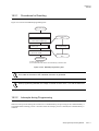
About This Manual
Objective
The primary objective of this LSI manual is to describe the features of this product including an
overview, CPU basic functions, interrupt, port, timer, serial interface, and other peripheral hardware
functions.
Each section consists of brief functional information, block diagrams and the details of control registers
including operation methods and setting examples.
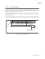
Structure of This Manual
Each section of this manual consists of a title, summary, main text, hint, precautions and warnings, and
references.
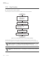
The layout and definition of each section are shown below.
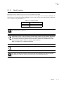
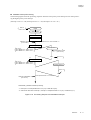
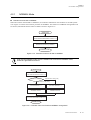
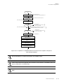
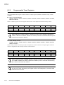
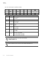
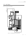
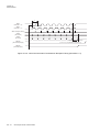
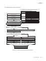
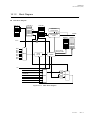
Header
Chapter number and
Chapter title
Section title
chapter 2
Basic CPU
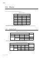
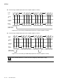
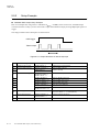
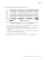
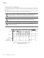
2.8 Reset
Sub section title
2.8.1
Main text
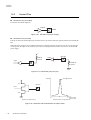
Reset operation
the CPU contents are reset and registers are intialized when the NRST pin (P
27) is pulled to low.
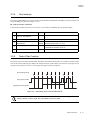
Initiating a Reset
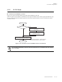
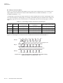
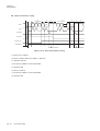
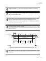
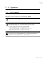
There are two methods to initiate areset.
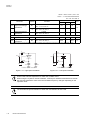
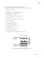
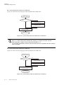
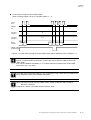
(1) Drive the NRST pin low for at least four clock cycles.
NTST pin should be holded "low" for more than 4 clock cycles (200 ns a
t a 20 NHz)
NRST pin
4 clock cycles
(200 ns at a 20 MHz)
Figure:2.8.1 MInimum Reset PUlse Width
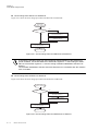
(2) Setting the P2OUT7 flag of the P2OUT register to "0" outputs low level at P
27 (NRST) pin. And transfering to reset by program (software reset) can be
executed. If the internal LSI is reset and register is initiated, the P2OUT
7 flag becomes "1" and reset is released.
Hint
Important information
from the text.
On this LSI, the starting mode is NORMAL mode that high oscillation i
s the base clock.
When the power voltage low circuit is connected to NTST pin, circuit t
hat gives pulse for enough low level time at sudeen unconnected. And r
set can be generated even if its pulse is low level as the oscillation
clock is under 4 clocks,take notice of noise.
Precautions and
warnings
Please be sure to read
the precautions to prevent
any loss of functionality or
damage to the chip.
footer
Page # and
section title.
II-48
Reset
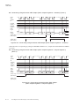
This page serves as an example to the explanations above. It may be different on an actual page.
<About This Manual - 1>
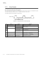
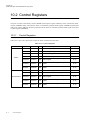
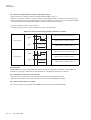
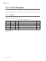
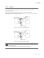
About
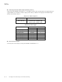
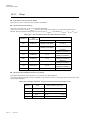
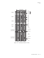
Register Table
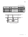
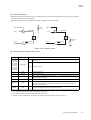
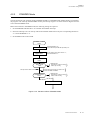
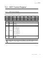
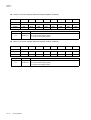
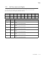
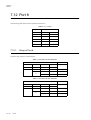
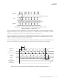
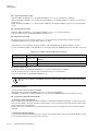
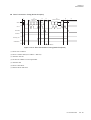
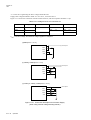
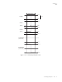
How to read the register table in each chapter is shown below.
Register name
Register symbol
Register address
Access size
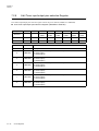
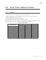
Chapter15
8-bit Timer
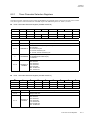
15.2.3 Timer Mode Registers
Values of the timer mode register contorl the operation, initialization, and clock source
selection of each timer. For setting clock sources, refer to [15.3 Clock Source Selection].
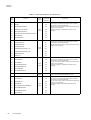
Timer 0 Mode Register (TM0MD: 0x0A200) [8-bit Access Register]
Register specification
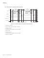
Each item is explained below.
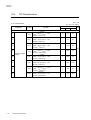
bp
7
6
Bit name
TM0CNE
TM0LDE
5
4
3
1
2
Reserved
-
0
TM0CK2-0
Initial value
0
0
0
0
0
0
0
0
Access
R/W
R/W
R
R
R/W
R/W
R/W
R/W
bp
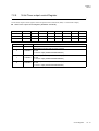
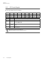
Bit name
7
TM0CNE
Timer 0 operation control
0: Deactivated
1: Activated
Description
6
TM0LDE
Binary counter initialization
0: Initialization release
1: Initialization
"0" is always read out.
5-4
-
3
Reserved
This bit must be set to "0".
TM0CK2-0
Clock source selection
000: IOCLK
001: IOCLK/8
010: IOCLK/32
011: Setting prohibited
100: Setting prohibited
101: Timer1 underflow
110: Timer2 underflow
111: IOCLK/128
2-0
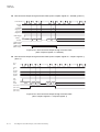
This register table serves as an example to the explanations above. It may be different on an actual table.
• bp
The bit position of each register is shown.
• Bit name
The bit symbol is shown.
There are following two kinds of statements in addition to the bit symbol.
Reserved : This is the reserved bit.
: This bit is not mounted.
• Initial value
The value of the bit immediately after reset release is shown with binary number.
When the value immediately after reset release is unfixed value, this item is indicated as "X".
• Access
"R" : This bit is readable.
"W" : This bit is writable.
• Description
The outline of the bit function and setting values are shown.
Access the bit according to the description in this item.
<About This Manual - 2>
Finding Desired Information
This manual provides three methods for finding the desired information quickly and easily.
1.Refer to the index at the front of the manual to locate the beginning of each section.
2.Refer to the table of contents at the front of the manual to locate the desired titles.
3.The chapter number and chapter title are located at the top corner of each page, and the section titles
are located at the bottom corner of each page.
Related Manuals
Note that the following documents related to MN101L series are available.
• "MN101L Series Instruction Manual"
<Describes the instruction set.>
• "MN101C/MN101E Series C Compiler User's Manual Usage Guide"
<Describes the installation, commands and options of the C Compiler.>
• "MN101C/MN101E Series C Compiler User's Manual Language Description"
<Describes the syntax of the C Compiler.>
• "MN101C/MN101E Series C Compiler User's Manual Library Reference"
<Describes the standard library of the C Compiler.>
• "MN101C/MN101E Series Cross-assembler User's Manual"
<Describes the assembler syntax and notation.>
• "PanaX EX Installation Manual"
<Describes the steps to install the Integrated Development Environment (DebugFactory Builder),
C compiler and the real-time OS. It also describes the procedure to setup the on-board environment.>
• "PanaX EX Commander User’s Manual"
< Describes the usage and notes on designing target board.>
Caution
The related documents listed above are subject to change without notice.
Use the latest version of each document for designing.
Contact Information
Please contact our sales division.
<About This Manual - 3>
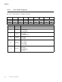
Chapter Table
Contents
Chapter 1 Overview
Chapter 2 CPU Basics
Chapter 3 Interrupts
Chapter 4 Clock/Mode/Voltage Control
Chapter 5 Watchdog Timer (WDT)
Chapter 6 Power Supply Voltage Detection
Chapter 7 I/O Port
Chapter 8 8-bit Timer
Chapter 9 16-bit Timer
Chapter 10 General-Purpose Time Base/Free-Running Timer
Chapter 11 RTC Time Base Timer (RTC-TBT)
Chapter 12 Real Time Clock (RTC)
0
1
2
3
4
5
6
7
8
9
10
11
12
Chapter 13 Serial Interface
Chapter 14 DMA Controller
Chapter 15 Buzzer
Chapter 16 A/D Converter (ADC)
Chapter 17 LCD
Chapter 18 ReRAM
Chapter 19 On-Board Debugger
Chapter 20 Appendix
13
14
15
16
17
18
19
20
Contents
Contents
0
Contents
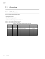
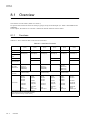
Chapter 1 Overview................................................................................................................ I-1
1.1 Hardware Features............................................................................................................................... I-2
1.2 Comparison of Product Specification.................................................................................................. I-7
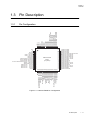
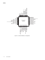
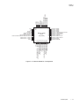
1.3 Pin Description .................................................................................................................................. I-11
1.3.1 Pin Configuration ................................................................................................................ I-11
1.3.2 Pin Description.................................................................................................................... I-15
1.4 Electrical Characteristics ...................................................................................................................
1.4.1 Absolute Maximum Ratings ...............................................................................................
1.4.2 Operating Condition............................................................................................................
1.4.3 DC Characteristics ..............................................................................................................
1.4.4 A/D Converter Characteristics ............................................................................................
1.4.5 Reset/Power supply Detection Characteristics....................................................................
1.4.6 ReRAM Program Condition ...............................................................................................
I-20
I-20
I-21
I-24
I-28
I-29
I-30
1.5 Package Dimension ........................................................................................................................... I-31
1.6 Cautions for Circuit Setup .................................................................................................................
1.6.1 Usage Notes ........................................................................................................................
1.6.2 Unused Pins.........................................................................................................................
1.6.3 Power Supply ......................................................................................................................
1.6.4 Power Supply Circuit ..........................................................................................................
I-35
I-35
I-36
I-38
I-39
Chapter 2 CPU....................................................................................................................... II-1
2.1 Overview ............................................................................................................................................ II-2
2.1.1 CPU Control Registers......................................................................................................... II-3
2.1.2 Data Registers (D0, D1, D2, D3) ......................................................................................... II-3
2.1.3 Address Registers (A0, A1) ................................................................................................. II-3
2.1.4 Stack Pointer (SP) ................................................................................................................ II-4
2.1.5 Program Counter (PC).......................................................................................................... II-4
2.1.6 Processor Status Word (PSW) ............................................................................................. II-5
2.1.7 Address Space ...................................................................................................................... II-7
2.1.8 Addressing Modes................................................................................................................ II-9
2.1.9 Bank Function .................................................................................................................... II-11
2.1.10 Special Function Register ................................................................................................ II-13
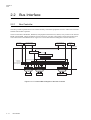
2.2 Bus Interface.....................................................................................................................................
2.2.1 Bus Controller ....................................................................................................................
2.2.2 Access Cycle ......................................................................................................................
2.2.3 Control Registers................................................................................................................
II-14
II-14
II-15
II-16
2.3 Extended Calculation Function ........................................................................................................ II-17
<Contents - 1>
2.3.1 Overview............................................................................................................................ II-17
2.3.2 Extended Calculation Control Register ............................................................................. II-18
2.4 Extended Calculation Instruction .....................................................................................................
2.4.1 About Extended Calculation Instruction............................................................................
2.4.2 MULWU 16-bit x 16-bit multiplication (unsigned) ..........................................................
2.4.3 MULW 16-bit x 16-bit multiplication (signed) .................................................................
2.4.4 DIVWU 32-bit / 16-bit division (unsigned) ......................................................................
2.4.5 BCDADD BCD addition (without carry) ..........................................................................
2.4.6 BCDADDC BCD addition (with carry).............................................................................
2.4.7 BCDSUB BCD subtraction (without carry) ......................................................................
2.4.8 BCDSUBC BCD subtraction (with carry).........................................................................
II-20
II-20
II-21
II-22
II-23
II-24
II-25
II-26
II-27
2.5 Reset .................................................................................................................................................
2.5.1 Reset function ....................................................................................................................
2.5.2 Reset sequence ...................................................................................................................
2.5.3 Oscillation Stabilization Wait Time ..................................................................................
II-28
II-28
II-29
II-30
Chapter 3 Interrupts.............................................................................................................. III-1
3.1 Overview ........................................................................................................................................... III-2
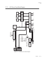
3.1.1 Block Diagram .................................................................................................................... III-3
3.1.2 Operation ............................................................................................................................ III-4
3.1.3 Maskable Interrupt Control Register Setup ...................................................................... III-15
3.1.4 Group Interrupt Control Register Setup............................................................................ III-17
3.2 Control Registers.............................................................................................................................
3.2.1 Non-maskable Interrupt (NMI) Control Register .............................................................
3.2.2 External Interrupt Control Register ..................................................................................
3.2.3 Peripheral Group Interrupt Control Register ....................................................................
3.2.4 Other Interrupt Control Register.......................................................................................
3.2.5 Block diagram of Peripheral function group interrupt......................................................
III-20
III-22
III-23
III-24
III-29
III-30
3.3 External Interrupts...........................................................................................................................
3.3.1 External Interrupt Control Registers.................................................................................
3.3.2 Rising (Falling) edge triggered interrupt ..........................................................................
3.3.3 Both edges triggered Interrupt ..........................................................................................
3.3.4 Key Interrupt.....................................................................................................................
3.3.5 Noise Filter Function ........................................................................................................
III-32
III-33
III-45
III-46
III-47
III-47
Chapter 4 Clock/ Mode/ Voltage Control ............................................................................ IV-1
4.1 Clock Control .................................................................................................................................... IV-2
4.1.1 Control Registers ................................................................................................................ IV-3
4.1.2 Change of the External Low-speed Oscillation Capability .............................................. IV-12
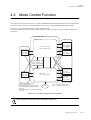
4.2 Mode Control Function ................................................................................................................... IV-13
<Contents - 2>
4.2.1 NORMAL Mode...............................................................................................................
4.2.2 SLOW Mode.....................................................................................................................
4.2.3 STANDBY Mode .............................................................................................................
4.2.4 Note for Transition to STANDBY Mode .........................................................................
IV-15
IV-17
IV-19
IV-23
4.3 Voltage Control ...............................................................................................................................
4.3.1 Overview...........................................................................................................................
4.3.2 Register List ......................................................................................................................
4.3.3 Power Supply Control Register ........................................................................................
4.3.4 Operation ..........................................................................................................................
IV-26
IV-26
IV-26
IV-27
IV-29
4.4 Mode/Voltage/Clock Transition...................................................................................................... IV-31
Chapter 5 Watchdog Timer (WDT) ...................................................................................... V-1
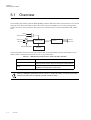
5.1 Overview ............................................................................................................................................ V-2
5.2 WDT Control Register ....................................................................................................................... V-3
5.2.1 WDT Control Register......................................................................................................... V-3
5.3 Operation............................................................................................................................................ V-4
5.3.1 WDT Operation ................................................................................................................... V-4
5.3.2 Setup Example ..................................................................................................................... V-5
Chapter 6 Power Supply Voltage Detection ....................................................................... VI-1
6.1 Overview ........................................................................................................................................... VI-2
6.1.1 Power Supply Voltage Detection Overview ....................................................................... VI-2
6.2 Control Register ................................................................................................................................ VI-3
6.2.1 Registers.............................................................................................................................. VI-3
6.2.2 Power Supply Voltage Detection Control Registers........................................................... VI-4
6.3 Setting Example ................................................................................................................................ VI-7
6.3.1 PSVD Setting Example....................................................................................................... VI-7
Chapter 7 I/O Port ............................................................................................................... VII-1
7.1 Overview ......................................................................................................................................... VII-2
7.1.1 I/O Port Overview............................................................................................................. VII-2
7.2 Control Registers............................................................................................................................. VII-3
7.2.1 Port n Output Registers..................................................................................................... VII-5
7.2.2 Port n Input Registers ....................................................................................................... VII-8
7.2.3 Port n Direction Control Registers.................................................................................. VII-12
7.2.4 Port n Pull-up Resistor Control Registers....................................................................... VII-15
7.2.5 Port n N-ch Open-drain Control Registers ..................................................................... VII-18
<Contents - 3>
7.2.6 Port n N-ch Drive Strength Selection Registers .............................................................
7.2.7 8-bit Timer output control Register ................................................................................
7.2.8 8-bit Timer input/output pins selection Register ............................................................
7.2.9 16-bit Timer output control Register ..............................................................................
7.2.10 16-bit Timer input/output pin selection Register..........................................................
7.2.11 Clock output / Clock output pin control Register .........................................................
7.2.12 Analog input Control Register 0 (Port1).......................................................................
7.2.13 Analog input Control Register 1 (Port8).......................................................................
7.2.14 Buzzer output / Buzzer output pin control Register .....................................................
VII-22
VII-25
VII-26
VII-27
VII-28
VII-29
VII-30
VII-31
VII-32
7.3 I/O Port Functions ......................................................................................................................... VII-33
7.4 Port 0 ............................................................................................................................................. VII-34
7.4.1 Setup of Port 0 ................................................................................................................ VII-34
7.5 Port 1 ............................................................................................................................................. VII-37
7.5.1 Setup of Port 1 ................................................................................................................ VII-37
7.6 Port 2 ............................................................................................................................................. VII-40
7.6.1 Setup of Port 2 ................................................................................................................ VII-40
7.7 Port 3 ............................................................................................................................................. VII-43
7.7.1 Setup of Port 3 ................................................................................................................ VII-43
7.8 Port 4 ............................................................................................................................................. VII-46
7.8.1 Setup of Port 4 ................................................................................................................ VII-46
7.9 Port 5 ............................................................................................................................................. VII-49
7.9.1 Setup of Port 5 ................................................................................................................ VII-49
7.10 Port 6 ........................................................................................................................................... VII-52
7.10.1 Setup of Port 6 .............................................................................................................. VII-52
7.11 Port 7 ........................................................................................................................................... VII-55
7.11.1 Setup of Port 7 .............................................................................................................. VII-55
7.12 Port 8 ........................................................................................................................................... VII-58
7.12.1 Setup of Port 8 .............................................................................................................. VII-58
Chapter 8 8-bit Timer........................................................................................................ VIII-1
8.1 Overview ........................................................................................................................................ VIII-2
8.1.1 Functions.......................................................................................................................... VIII-2
8.1.2 8-bit Timer Block Diagram.............................................................................................. VIII-3
8.2 8-bit Timer Control Registers ........................................................................................................
8.2.1 Timer Prescaler Selection Registers ................................................................................
8.2.2 Programmable Timer Registers .......................................................................................
8.2.3 Timer Mode Registers .....................................................................................................
VIII-4
VIII-5
VIII-8
VIII-9
<Contents - 4>
8.3 8-bit Timer ................................................................................................................................... VIII-15
8.3.1 Operation ....................................................................................................................... VIII-15
8.3.2 Setup Example ............................................................................................................... VIII-19
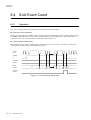
8.4 8-bit Event Count ......................................................................................................................... VIII-20
8.4.1 Operation ....................................................................................................................... VIII-20
8.4.2 8-bit Event Count Setup Example ................................................................................. VIII-22
8.5 8-bit Timer Pulse Output.............................................................................................................. VIII-23
8.5.1 Operation ....................................................................................................................... VIII-23
8.5.2 Setup Example ............................................................................................................... VIII-24
8.6 8-bit PWM Output........................................................................................................................
8.6.1 Operation (Timer 0, Timer 2 and Timer 4)....................................................................
8.6.2 Setup Example ...............................................................................................................
8.6.3 PWM Output With Additional Pulse (Timer 0, Timer 2, Timer 4) ...............................
VIII-25
VIII-25
VIII-27
VIII-28
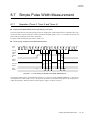
8.7 Simple Pulse Width Measurement ............................................................................................... VIII-29
8.7.1 Operation (Timer 0, Timer 2 and Timer 4).................................................................... VIII-29
8.7.2 Setup Example ............................................................................................................... VIII-30
8.8 8-bit Timer Cascade Connection.................................................................................................. VIII-31
8.8.1 Operation ....................................................................................................................... VIII-31
8.8.2 Setup Example ............................................................................................................... VIII-33
Chapter 9 16-bit Timer......................................................................................................... IX-1
9.1 Overview ........................................................................................................................................... IX-2
9.2 16-bit Timer Control Registers ......................................................................................................... IX-4
9.2.1 Programmable Timer Registers .......................................................................................... IX-6
9.2.2 Timer Mode Registers ...................................................................................................... IX-10
9.3 16-bit Timer .................................................................................................................................... IX-21
9.3.1 Operation .......................................................................................................................... IX-21
9.3.2 Setup Example .................................................................................................................. IX-24
9.4 16-bit Event Count .......................................................................................................................... IX-25
9.4.1 Operation .......................................................................................................................... IX-25
9.4.2 Setup Example .................................................................................................................. IX-28
9.5 16-bit Timer Pulse Output............................................................................................................... IX-29
9.5.1 Operation .......................................................................................................................... IX-29
9.5.2 Setup Example .................................................................................................................. IX-30
9.6 16-bit Standard PWM Output (with Continuously Variable Duty) ................................................ IX-31
9.6.1 Operation .......................................................................................................................... IX-31
9.6.2 Setup Example .................................................................................................................. IX-34
9.7 16-bit High-Precision PWM Output (with Continuously Variable Period/Duty)........................... IX-35
<Contents - 5>
9.7.1 Operation .......................................................................................................................... IX-35
9.7.2 Setup Example .................................................................................................................. IX-38
9.8 16-bit Timer Capture Function........................................................................................................ IX-39
9.8.1 Operation .......................................................................................................................... IX-39
9.8.2 Setup Example .................................................................................................................. IX-46
9.9 16-bit Standard IGBT Output (with Variable Duty) ....................................................................... IX-47
9.9.1 Operation .......................................................................................................................... IX-47
9.9.2 Setup Example .................................................................................................................. IX-50
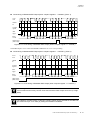
9.10 16-bit High-Precision IGBT Output (with Variable Period/Duty) ............................................... IX-51
9.10.1 Operation ........................................................................................................................ IX-51
9.10.2 Setup Example ................................................................................................................ IX-57
9.11 IGBT Output with Dead Time ...................................................................................................... IX-58
9.11.1 Operation ........................................................................................................................ IX-58
9.11.2 Setup Example ................................................................................................................ IX-62
Chapter 10 General-Purpose Time Base/Free-Running Timer ............................................ X-1
10.1 Overview .......................................................................................................................................... X-2
10.1.1 Functions............................................................................................................................ X-2
10.1.2 Block Diagram ................................................................................................................... X-3
10.2 Control Registers..............................................................................................................................
10.2.1 Control Registers ...............................................................................................................
10.2.2 Programmable Timer Registers .........................................................................................
10.2.3 Timer 6 Enable Register ....................................................................................................
10.2.4 Timer Mode Register .........................................................................................................
X-4
X-4
X-5
X-6
X-7
10.3 8-bit Free-running Timer.................................................................................................................. X-8
10.3.1 Operation ........................................................................................................................... X-8
10.3.2 Setup Example ................................................................................................................. X-11
10.4 Time Base Timer............................................................................................................................ X-12
10.4.1 Operation ......................................................................................................................... X-12
10.4.2 Setup Example ................................................................................................................. X-14
Chapter 11 RTC Time Base Timer (RTC-TBT) ................................................................. XI-1
11.1 Overview ......................................................................................................................................... XI-2
11.1.1 Functions........................................................................................................................... XI-2
11.2 Control Register ..............................................................................................................................
11.2.1 RTC-TBT Control Register ..............................................................................................
11.2.2 RTC-TBT Register ...........................................................................................................
11.2.3 RTC-TBT Frequency Adjustment Register ......................................................................
XI-3
XI-4
XI-6
XI-7
<Contents - 6>
11.3 RTC-TBT Operation ....................................................................................................................... XI-9
11.3.1 RTC-TBT Operation......................................................................................................... XI-9
11.3.2 Operation Setting Example............................................................................................. XI-10
Chapter 12 Real Time Clock (RTC) ................................................................................... XII-1
12.1 Overview ....................................................................................................................................... XII-2
12.2 Control Registers........................................................................................................................... XII-3
12.2.1 RTC Control Register ..................................................................................................... XII-4
12.2.2 Alarm 0 Interrupt Registers ............................................................................................ XII-5
12.2.3 Alarm 1 Interrupt Registers ............................................................................................ XII-7
12.2.4 Periodic Interrupt Control Register............................................................................... XII-10
12.2.5 Clock Registers ............................................................................................................. XII-11
12.2.6 RTC Status Register...................................................................................................... XII-14
12.3 RTC Operation ............................................................................................................................ XII-15
12.3.1 Clock Data Reading Procedure..................................................................................... XII-16
12.3.2 Setup Example .............................................................................................................. XII-17
Chapter 13 Serial Interface................................................................................................ XIII-1
13.1 Overview ...................................................................................................................................... XIII-2
13.1.1 Functions........................................................................................................................ XIII-3
13.1.2 Block Diagram ............................................................................................................... XIII-5
13.2 Control Registers.......................................................................................................................... XIII-7
13.2.1 Registers......................................................................................................................... XIII-7
13.2.2 Input/Output Pin Control Register................................................................................. XIII-9
13.2.3 Receive Data Buffer..................................................................................................... XIII-10
13.2.4 Transmit Data Buffer ................................................................................................... XIII-10
13.2.5 Mode Register.............................................................................................................. XIII-11
13.2.6 Status Register ............................................................................................................. XIII-19
13.2.7 Address Setting Register.............................................................................................. XIII-22
13.2.8 BRTM Operation Mode Setting Register .................................................................... XIII-22
13.2.9 BRTM Operation Enable Register............................................................................... XIII-23
13.2.10 BRTM Clock Select Register .................................................................................... XIII-24
13.2.11 BRTM Compare Register .......................................................................................... XIII-27
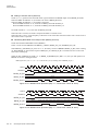
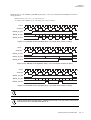
13.3 Clock-Synchronous Communication .........................................................................................
13.3.1 Form.............................................................................................................................
13.3.2 Operation .....................................................................................................................
13.3.3 Operation Timing.........................................................................................................
13.3.4 Setting Procedure.........................................................................................................
XIII-28
XIII-28
XIII-29
XIII-39
XIII-41
13.4 Full-duplex UART Communication .......................................................................................... XIII-46
13.4.1 Communication Form .................................................................................................. XIII-46
<Contents - 7>
13.4.2 Operation ..................................................................................................................... XIII-48
13.4.3 Timing.......................................................................................................................... XIII-52
13.4.4 Setting procedure ......................................................................................................... XIII-54
13.5 IIC Communication....................................................................................................................
13.5.1 Format..........................................................................................................................
13.5.2 Operation .....................................................................................................................
13.5.3 Timing..........................................................................................................................
13.5.4 Setup Example .............................................................................................................
XIII-56
XIII-56
XIII-57
XIII-62
XIII-68
Chapter 14 DMA Controller ............................................................................................. XIV-1
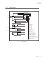
14.1 Overview ...................................................................................................................................... XIV-2
14.1.1 Block Diagram ............................................................................................................... XIV-3
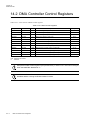
14.2 DMA Controller Control Registers .............................................................................................. XIV-4
14.2.1 DMA Control Register................................................................................................... XIV-5
14.2.2 DMA Source Address Register...................................................................................... XIV-9
14.2.3 DMA Destination Address Register ............................................................................ XIV-10
14.2.4 DMA Transfer Word Count Register .......................................................................... XIV-11
14.3 DMA Data Transfer ................................................................................................................... XIV-12
14.3.1 Single Transfer Mode .................................................................................................. XIV-12
14.3.2 Burst Transfer Mode .................................................................................................... XIV-13
Chapter 15 Buzzer.............................................................................................................. XV-1
15.1 Overview ....................................................................................................................................... XV-2
15.2 Control Register ............................................................................................................................ XV-3
15.2.1 Registers.......................................................................................................................... XV-3
15.2.2 Buzzer Control Register.................................................................................................. XV-4
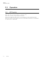
15.3 Operation....................................................................................................................................... XV-5
15.3.1 Operation ........................................................................................................................ XV-5
15.3.2 Setup Example ................................................................................................................ XV-6
Chapter 16 A/D Converter (ADC) .................................................................................... XVI-1
16.1 Overview ...................................................................................................................................... XVI-2
16.1.1 Functions........................................................................................................................ XVI-2
16.1.2 Block Diagram ............................................................................................................... XVI-3
16.2 Control Registers..........................................................................................................................
16.2.1 Registers.........................................................................................................................
16.2.2 Control Registers ...........................................................................................................
16.2.3 Data Buffers...................................................................................................................
XVI-4
XVI-4
XVI-5
XVI-7
<Contents - 8>
16.3 Operation...................................................................................................................................... XVI-8
16.3.1 Setup ............................................................................................................................ XVI-10
16.3.2 Setup Procedure ........................................................................................................... XVI-12
16.3.3 Cautions ....................................................................................................................... XVI-13
Chapter 17 LCD ............................................................................................................... XVII-1
17.1 Overview ..................................................................................................................................... XVII-2
17.1.1 LCD Driver Circuit Block Diagram ............................................................................. XVII-3
17.2 Control Registers......................................................................................................................... XVII-4
17.2.1 LCD Mode Control Registers ....................................................................................... XVII-5
17.2.2 LCD Port Control Registers.......................................................................................... XVII-9
17.3 Operation................................................................................................................................... XVII-17
17.3.1 LCDDRV Operation ................................................................................................... XVII-17
17.3.2 Voltage Booster Circuit (BSTVOL) ........................................................................... XVII-18
17.3.3 Reference Voltage Circuit (REFVOL) ....................................................................... XVII-18
17.3.4 LCD Drive Voltage Selection..................................................................................... XVII-19
17.3.5 LCD Frame Frequency Setup ..................................................................................... XVII-24
17.3.6 Setup Examples of REFVOL and BSTVOL .............................................................. XVII-25
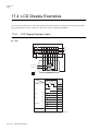
17.4 LCD Display Examples............................................................................................................. XVII-26
17.4.1 LCD Display Example (static).................................................................................... XVII-26
17.4.2 LCD Operation Setup Example (static) ...................................................................... XVII-28
17.4.3 LCD Display Example (1/2 duty) ............................................................................... XVII-29
17.4.4 LCD Operation Setup (1/2 duty) ................................................................................ XVII-31
17.4.5 LCD Display Example (1/3 duty) ............................................................................... XVII-32
17.4.6 LCD Operation Setup (1/3 duty) ................................................................................ XVII-34
17.4.7 LCD Display Example (1/4 duty) ............................................................................... XVII-35
17.4.8 LCD Operation Setup (1/4 duty) ................................................................................ XVII-37
Chapter 18 ReRAM........................................................................................................ XVIII-1
18.1 Overview of ReRAM ................................................................................................................
18.1.1 ReRAM Rewriting Method ........................................................................................
18.1.2 ReRAM Area ..............................................................................................................
18.1.3 Data Protection Function ............................................................................................
XVIII-2
XVIII-2
XVIII-3
XVIII-3
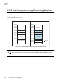
18.2 Self-programming Rewriting Method....................................................................................... XVIII-4
18.2.1 Procedures for Rewriting ............................................................................................ XVIII-5
18.2.2 Interrupts during Programming .................................................................................. XVIII-5
18.3 ReRAM Control Registers ........................................................................................................ XVIII-6
18.4 Command Library ..................................................................................................................... XVIII-7
<Contents - 9>
Chapter 19 On-Board Debugger ....................................................................................... XIX-1
19.1 Overview ...................................................................................................................................... XIX-2
19.2 List of on-board debugging functions .......................................................................................... XIX-3
Chapter 20 Appendix ......................................................................................................... XX-1
20.1 Symbol Definitions ....................................................................................................................... XX-2
20.2 Instruction set ................................................................................................................................ XX-5
20.3 Instruction map............................................................................................................................ XX-11
<Contents - 10>
<Contents - 11>
I..
Chapter 1 Overview
1
Chapter 1
Overview
1.1 Hardware Features
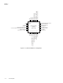
MN101LR05D is described in this LSI user's manual.
For MN101LR04D, MN101LR03D and MN101LR02D, refer to [1.2 Comparison of Product Specification] and
[1.3.1 Pin Configuration].
Features
In this document, the divided clock and the frequency of it are described as follows:
Divided clock: Clock name/n (n: division ratio)
Frequency : fclock name
• CPU Core
- AM13L core
- LOAD-STORE architecture (3- or 4-stage Pipeline)
• Machine Cycle and Operating Voltage
- High-Speed mode
100 ns / 10 MHz (Max) (VDD30: 1.8 V to 3.6 V)
1.0 µs / 1 MHz (Max) (VDD30: 1.3 V to 3.6 V)
- Low-Speed Mode
25 µs / 40 kHz (Max)
(VDD30: 1.1 V to 3.6 V)
• Operating Mode
- NORMAL mode (High-Speed mode)
- SLOW mode
(Low-Speed mode)
- HALT mode
(High-Speed/Low-Speed mode)
- STOP mode
• Embedded Memory
- ROM (ReRAM) : 64 KB (Programmable area: 62 KB, Data area: 2 KB)
- RAM
: 4 KB
• ReRAM Specification
- Program voltage (VDD30) : 1.8 V to 3.6 V
- Program cycles
: 1 K (Program area), 100 K (Data area)
- Data is rewritable in bytes without data erase.
• Clock Oscillator (4 circuits)
- External Low-Speed Oscillation (SOSCCLK) : 32.768 kHz (crystal or ceramic)
- External High-Speed Oscillation (HOSCCLK): up to 10 MHz (crystal or ceramic)
- Internal Low-Speed Oscillation (SRCCLK) :
40 kHz ± 20 % (VDD30: 1.1 V to 3.6 V)
- Internal High-Speed Oscillation (HRCCLK) :
10/8 MHz ± 3 % (VDD30: 1.8 V to 3.6 V)
1 MHz ± 10 % (VDD30: 1.3 V to 3.6 V)
* MN101LR02D does not have external high-speed oscillation (HOSCCLK).
• Internal Operating Clock
- System Clock (SYSCLK): 10 MHz (Max)
SYSCLK is generated by dividing HCLK or SCLK, and the division ratio is 1, 2, 4, 8, 16 or 32.
HCLK: HOSCCLK or HRCCLK
SCLK: SOSCCLK or SRCCLK
* MN101LR02D cannot be selected HOSCCLK.
I-2
Hardware Features
Chapter 1
Overview
• Interrupt Circuit
- 31 internal interrupts (except for NMI)
- 8 external interrupts
* MN101LR02D:
- 29 internal interrupts (except for NMI)
- 3 external interrupts
• DMA (1 channel)
- Data transfer size
: 8 bits/16 bits
- Maximum transfer counts: 1023
- Activation trigger
: external interrupts / internal interrupts / software (setting the DMA start bit)
• Watchdog Timer (WDT)
- Function
: 1st watchdog time-out generates NMI, and 2nd consecutive time-out generates a LSI reset.
- Clock Source : WDTCLK (SOSCCLK or SRCCLK)
• Timer Counter: 13 units
- General-purpose 8-bit timer (Timer 0/1/2/3/4/5) : 6 units
- General-purpose 16-bit timer (Timer 7/8/9)
: 3 units
- 8-bit free-run (Timer 6) /Time-base timer
: 1 unit each
- RTC time base timer (RTC-TBT)
: 1 unit
- Real Time Clock (RTC)
: 1 unit
<Timer 0>
- Function
: Square wave output, additional pulse PWM output, event count,
simple pulse width measurement
- Clock Source : HCLK, HCLK/4, HCLK/16, HCLK/32, HCLK/64, SCLK, SYSCLK/2, SYSCLK/4,
and TM0IO input
<Timer 1 >
- Function
: Square wave output, event count, 16-bit cascade connection (connected with Timer 0)
- Clock Source : HCLK, HCLK/4, HCLK/16, HCLK/64, HCLK/128, SCLK, SYSCLK/2, SYSCLK/8,
and TM1IO input
<Timer 2>
- Function
: Square wave output, additional pulse PWM output, event count,
simple pulse width measurement
- Clock Source : HCLK, HCLK/4, HCLK/16, HCLK/32, HCLK/64, SCLK, SYSCLK/2, SYSCLK/4,
and TM2IO input
<Timer 3 >
- Function
: Square wave output, event count, 16-bit cascade connection (connected with Timer 2)
- Clock Source : HCLK, HCLK/4, HCLK/16, HCLK/64, HCLK/128, SCLK, SYSCLK/2, SYSCLK/8,
and TM3IO input
<Timer 4>
- Function
: Square wave output, additional pulse PWM output, event count,
simple pulse width measurement
- Clock Source : HCLK, HCLK/4, HCLK/16, HCLK/32, HCLK/64, SCLK, SYSCLK/2, SYSCLK/4,
and TM4IO input
<Timer 5 >
- Function
: Square wave output, event count, 16-bit cascade connection (connected with Timer 4)
- Clock Source : HCLK, HCLK/4, HCLK/16, HCLK/64, HCLK/128, SCLK, SYSCLK/2, SYSCLK/8,
and TM5IO input
* MN101LR02D cannot be used square wave output, event count and TM5IO.
Hardware Features
I-3
Chapter 1
Overview
<Timer 6>
- Function
: One-minute timer can be generated in combination with a time base timer.
- Clock Source : HCLK, HCLK/27, HCLK/213, SYSCLK, SCLK, SCLK/27, SCLK/213
<Time Base Timer>
- Function
: An interrupt can be generated at a given set time.
- Clock Source : HCLK and SCLK
- Interrupt generation cycle: 2N/fHCLK, 2N/fSCLK (N = 7, 8, 9, 10, 12, 13, 14, 15)
<Timer 7>
- Function
: Square wave output, PWM output (duty/cycle are programmable), one-shot pulse output,
IGBT output, event count, and input capture
- Clock Source : Generated clock by dividing HCLK, SYSCLK, SCLK, or TM7IO input by 1, 2, 4 or 16.
<Timer 8 >
- Function
: Square wave output, PWM output (duty/cycle are programmable), event count,
and input capture
- Clock Source : Generated clock by dividing HCLK, SYSCLK, SCLK, or TM8IO input by 1, 2, 4 or 16.
<Timer 9 >
- Function
: Square wave output, PWM output (duty/cycle are programmable), event count,
and input capture
- Clock Source : Generated clock by dividing HCLK, SYSCLK, SCLK, or TM9IO input by 1, 2, 4 or 16.
* MN101LR03D and MN101LR02D
cannot be used square wave output, PWM output, event count and TM9IO.
<RTC time base timer (RTC-TBT)>
- Function
: Clock generation for the Real Time Clock (RTC)
Frequency correction
(Correction Range: ±488 ppm to ±31220 ppm, Accuracy: approx. 0.48 ppm to 30.52 ppm)
- Clock Source : SOSCCLK or SRCCLK
<Real Time Clock (RTC)>
- Function
: Calendar calculation, adjustment of leap year
Periodic interrupt (0.5 s, 1 s, 1 min, and 1 hour)
Alarm0 interrupt (date/month/minute), Alarm1 interrupt (month/day/hour/minute)
• Buzzer Output/Inverted Buzzer Output
- Output frequency: fHCLK/2M (M = 9, 10, 11, 12, 13, 14), fSCLK/2N (N = 3, 4)
* MN101LR02D can be used inverted buzzer output only.
• Serial Interface: 4 units
<Serial Interface 0, 1> (Full duplex UART/Clock synchronous serial)
- Function:
Full duplex UART:
Parity check, Detection of overrun error/framing error, Selectable transfer bits of 7 or 8
Clock synchronous serial (SPI compatible):
2,3 or 4-wire communication, MSB/LSB first selectable, multiple bytes transmission is available.
- Clock Source: external clock, dedicated baud rate timer
<Serial Interface 2, 3> (Multi-master IIC/Clock synchronous serial)
- Function:
Multi-master IIC
Clock synchronous serial (SPI compatible):
2,3 or 4-wire communication, MSB/LSB first selectable, multiple bytes transmission is available.
- Clock Source: external clock, dedicated baud rate timer
I-4
Hardware Features
Chapter 1
Overview
* MN101LR03D
Serial Interface 3: Clock synchronous serial cannot be used 3 and 4-wire communication,
and is not compatible with SPI. (Chip select pin is not assigned.)
* MN101LR02D
Serial Interface 1: Not implemented
Serial Interface 3: Clock synchronous serial cannot be used 4-wire communication,
and is not compatible with SPI. (Chip select pin is not assigned.)
• A/D Converter (ADC): 1 unit
- Resolution
: 12 bits
- Analog signal input channel: 8 channels
* MN101LR04D
: 6 channels
* MN101LR03D
: 4 channels
* MN101LR02D
: 3 channels
• I/O ports: 69 pins
- Selectable N-channel transistor drive strength: 55 pins
* MN101LR04D: 53 pins (selectable N-channel transistor drive strength: 41 pins)
* MN101LR03D: 37 pins (selectable N-channel transistor drive strength: 27 pins)
* MN101LR02D: 22 pins (selectable N-channel transistor drive strength: 19 pins)
• Clock Output
- HCLK, SCLK, SYSCLK or RTCCLK can be output.
• Automatic Reset Circuit
• Low-voltage Detection Circuit (LVI)
• LCD Driver
- 43 segment outputs, 4 common outputs (39 segment outputs, 8 common outputs)
- Display mode: Static, 1/2 to 1/8 duty
- Bias
: 1/2, 1/3 (Built-in boost/ External resistor divider)
* MN101LR04D
31 segment outputs
4 common outputs
Display mode: Static, 1/2 to 1/4 duty
* MN101LR03D
21 segment outputs
4 common outputs
Display mode: Static, 1/2 to 1/4 duty
* MN101LR02D does not have LCD driver function.
Hardware Features
I-5
Chapter 1
Overview
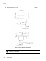
• Package
- MN101LR05D: TQFP080-P-1212
- MN101LR04D: TQFP064-P-1010
- MN101LR03D: TQFP048-P-0707
- MN101LR02D: HQFN032-A-0505
(12 mm square, 0.5 mm pitch, halogen free)
(10 mm square, 0.5 mm pitch, halogen free)
( 7 mm square, 0.5 mm pitch, halogen free)
( 5 mm square, 0.5 mm pitch, halogen free)
Panasonic "halogen free" semiconductor products refer to the products made of molding resin and interposer
which conform to the following standards.
- Bromine
: 900 ppm (Maximum Concentration Value)
- Chlorine
: 900 ppm (Maximum Concentration Value)
- Bromine + Chlorine: 1500 ppm (Maximum Concentration Value)
The above-mentioned standards are based on the numerical value described in IEC61249-2-21.
Antimony and its compounds are not added intentionally.
• Operating Ambient Temperature
- Ta = -40 °C to 85 °C
I-6
Hardware Features
Chapter 1
Overview
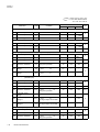
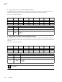
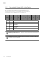
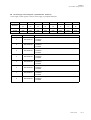
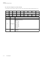
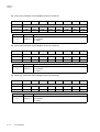
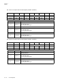
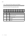
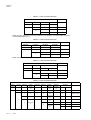
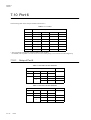
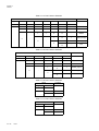
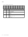
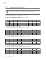
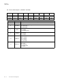
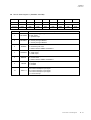
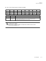
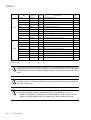
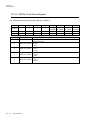
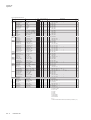
1.2 Comparison of Product Specification
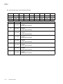
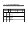
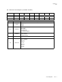
Table:1.2.1 Functions
Function
Specification
MN101LR05D
MN101LR04D
MN101LR03D
MN101LR02D
Port
I/O port
69 pins
53 pins
37 pins
22 pins
55 pins
41 pins
27 pins
19 pins
Internal interrupt
31
31
31
29
External interrupt
8
(7:IRQ0-6, 1:KEY0-7)
8
(7:IRQ0-6, 1:KEY1-7)
8
(7:IRQ0-6, 1:KEY1-5)
3
(2:IRQ4-5, 1:KEY1-7)
Timer 5
Timer I/O
TM5IO
TM5IO
TM5IO
- (*1)
Timer 9
Timer I/O
TM9IO
TM9IO
- (*1)
- (*1)
√
√
√
-
Serial communication
pins
SBO3/SDA3
SBT3/SCL3
SBI3
SBCS3
SBO3/SDA3
SBT3/SCL3
SBI3
SBCS3
SBO3/SDA3
SBT3/SCL3
-
SBO3/SDA3
SBT3/SCL3
SBI3
-
Clock synchronous
2, 3 or 4-wire
2, 3 or 4-wire
2-wire
2 or 3-wire
SPI compatible
√
√
- (*2)
- (*2)
Buzzer
Buzzer output
/Inverted buzzer output
BUZ
NBUZ
BUZ
NBUZ
BUZ
NBUZ
NBUZ
ADC
Analog input
8 pins (AN0-7)
6 pins (AN2-7)
4 pins (AN2-5)
3 pins (AN3-5)
LCD driver
Segment output
43 pins (SEG0-42)
/39 pins (SEG4-42)
31 pins (SEG0-30)
21 pins (SEG0-20)
-
Common output
4 pins (COM0-3)
/8 pins (COM0-7)
4 pins (COM0-3)
4 pins (COM0-3)
-
Oscillation
HOSCCLK
SOSCCLK
HRCCLK
SRCCLK
HOSCCLK
SOSCCLK
HRCCLK
SRCCLK
HOSCCLK
SOSCCLK
HRCCLK
SRCCLK
SOSCCLK
HRCCLK
SRCCLK
Package
80pinTQFP
64pinTQFP
48pinTQFP
32pinHQFN
N-channel transistor
drive strength
Interrupt
Serial
interface 1
Serial
interface 3
*1 Timer function is available.
*2 Chip select pin is not assigned.
Comparison of Product Specification
I-7
Chapter 1
Overview
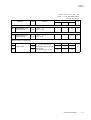
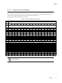
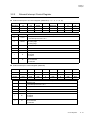
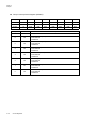
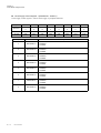
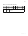
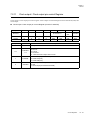
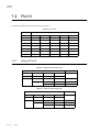
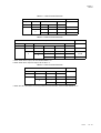
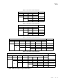
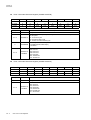
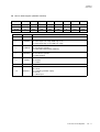
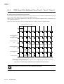
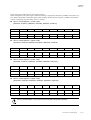
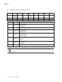
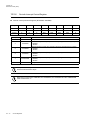
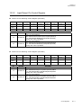
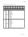
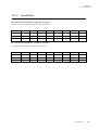
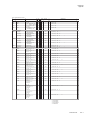
Table:1.2.2 Functions of I/O Port
MN101LR05D
MN101LR04D
MN101LR03D
MN101LR02D
I/O
Port
7
6
5
4
3
2
1
0
7
6
5
4
3
2
1
0
7
6
5
4
3
2
1
0
7
6
5
4
3
2
1
0
Port0
√
√
√
√
√
√
√
√
√
√
√
√
√
√
-
-
-
-
√
√
-
-
-
-
-
√
√
√
-
-
-
-
Port1
√
√
√
√
√
√
√
√
√
√
√
√
√
√
-
-
-
-
√
√
√
√
-
-
-
-
√
√
√
-
-
-
Port2
√
√
√
√
√
√
√
√
√
√
-
-
-
-
√
√
√
√
-
-
-
-
-
-
√
-
-
-
-
-
-
-
Port3
√
√
√
√
√
√
√
√
√
√
√
√
√
√
√
√
√
√
√
√
√
√
√
√
√
√
√
√
-
-
-
-
Port4
√
√
√
√
√
√
√
√
√
√
√
√
√
√
√
√
-
-
-
√
√
√
√
√
-
-
-
√
√
√
√
√
Port5
√
√
√
√
√
√
√
√
√
√
√
-
-
-
-
√
√
√
√
-
-
-
-
-
√
√
√
-
-
-
-
-
Port6
√
√
√
√
√
√
√
√
√
√
√
√
√
√
√
√
-
-
-
-
√
√
√
√
√
√
√
√
-
-
-
-
Port7
√
√
√
√
√
√
√
√
-
-
-
-
√
√
√
√
-
-
-
-
√
√
√
√
-
-
-
-
-
-
-
-
Port8
-
-
√
√
√
√
√
√
-
-
√
√
√
√
√
√
-
-
√
√
√
√
√
√
-
-
-
-
-
-
-
-
√
: implemented I/O port
√
: implemented I/O port (selectable N-channel transistor drive strength)
-
: not implemented
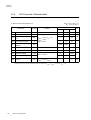
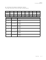
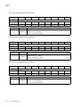
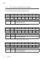
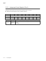
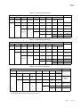
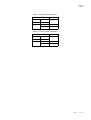
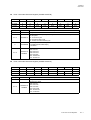
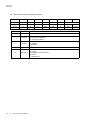
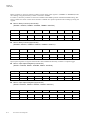
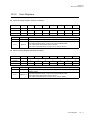
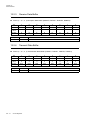
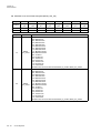
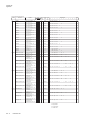
Table:1.2.3 Functions of LCD Control
MN101LR05D
I/O
Port
7
Port2
-
6
5
4
3
MN101LR04D
2
1
0
SEG SEG SEG SEG SEG SEG SEG
36
37
38
39
40
41
42
MN101LR03D
7
6
5
4
3
2
-
SEG
28
-
-
-
-
1
0
SEG SEG
29
30
7
6
5
4
3
2
1
0
-
SEG
20
-
-
-
-
-
-
Port3 SEG SEG SEG SEG SEG SEG SEG SEG SEG SEG SEG SEG SEG SEG SEG SEG SEG SEG SEG SEG SEG SEG SEG SEG
28
29
30
31
32
33
34
35
20
21
22
23
24
25
26
27
12
13
14
15
16
17
18
19
Port4 SEG SEG SEG SEG SEG SEG SEG SEG SEG SEG SEG SEG SEG SEG SEG SEG
20
21
22
23
24
25
26
27
12
13
14
15
16
17
18
19
Port5 SEG SEG SEG SEG SEG SEG SEG SEG SEG SEG SEG
12
13
14
15
16
17
18
19
8
9
10
-
-
-
-
-
-
-
SEG SEG SEG SEG
11
4
5
6
SEG SEG SEG SEG SEG
7
8
9
10
11
-
-
-
-
-
Port6 SEG SEG SEG SEG SEG SEG SEG SEG SEG SEG SEG SEG SEG SEG SEG SEG
4
5
6
7
8
9
10
11
0
1
2
3
4
5
6
7
-
-
-
-
SEG SEG SEG SEG
0
1
2
3
Port7 COM COM COM COM COM COM COM COM
0
1
2
3
4/
5/
6/
7/
SEG SEG SEG SEG
0
1
2
3
-
-
-
-
-
-
COM COM COM COM
0
1
2
3
Port8
-
-
-
-
-
-
VLC VLC
2
3
-
C2
C1
-
-
VLC1
-
-
COM COM COM COM
0
1
2
3
VLC VLC
2
3
C2
VLC1
C1
-
-
VLC VLC
2
3
C2
C1
VLC1
-: not implemented
LCD control function is not implemented in MN101LR02D.
Set “0” to the registers and bits corresponding to the functions which are not implemented.
..
I-8
Comparison of Product Specification
-
-
Chapter 1
Overview
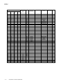
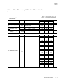
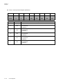
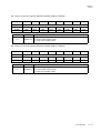
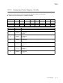
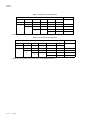
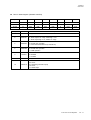
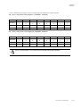
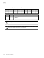
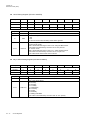
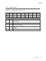
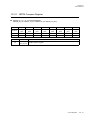
Table:1.2.4 Pin Functions
Pin No.
MN101 MN101 MN101 MN101
LR05D LR04D LR03D LR03D
Power supply
/Oscillations
/Reset
/Mode control
Port
External
interrupt
/KEY interrupt
1
1
1
32
2
2
2
1
XI
3
3
3
2
XO
4
4
4
3
NATRON
5
5
5
4
NRST
P27
6
6
6
OSC1
P80
IRQ2A
7
7
7
OSC2
P81
IRQ3A
Timer
Serial
interface
Buzzer
/Clock output
A/D
VSS
8
P00
TM9IOC
9
P01
TM4IOB
10
8
P02
TM2IOB/TM8IOC
BUZB
11
9
P03
TM0IOB/TM7IOC
NBUZB
12
10
8
5
P04
13
11
9
6
P05
14
12
7
P06
15
13
TM7IOA
SBO3A/SDA3A
TM0IOA/TM2IOA SBT3A/SCL3A
P07
TM8IOB
SBI3A
TM9IOA
SBCS3A
CLKOUTA
16
P10
IRQ0A/KEY0A
AN0
17
P11
IRQ1A/KEY1A
AN1
18
14
10
19
15
11
8
P12
IRQ4C/KEY2A
AN2
P13
IRQ5C/KEY3A
AN3
20
16
12
9
21
17
13
10
DMOD
22
18
14
11
OCD_CLK
P14
IRQ4A/KEY4A
AN4
23
19
15
12
24
20
OCD_DATA
P15
IRQ5A/KEY5A
AN5
P16
IRQ6A/KEY6A
25
21
AN6
P17
KEY7A
AN7
VREFP
26
22
P20
TM1IOB/TM9IOB
27
23
P21
TM5IOA
28
P22
SBI2B
29
P23
SBO2B/SDA2B
30
P24
SBT2B/SCL2B
31
P25
SBCS2B
32
24
16
P26
SBI1A/RXD1A
33
25
17
P30
SBO1A/TXD1A
34
26
18
P31
SBT1A
35
27
19
P32
SBCS1A
36
28
20
37
29
21
13
P34
38
30
22
14
P35
SBI0B/RXD0B
SBO0B/TXD0B
P33
BUZA
TM4IOA/TM7IOB
NBUZA
39
31
23
15
P36
40
32
24
16
P37
SBT0B
41
33
25
17
P40
SBCS0B
42
34
26
18
P41
SBI2A
43
35
27
19
P42
SBO2A/SDA2A
44
36
28
20
P43
SBT2A/SCL2A
Comparison of Product Specification
I-9
Chapter 1
Overview
Pin No.
Power supply
/Oscillations
MN101 MN101 MN101 MN101
/Reset
LR05D LR04D LR03D LR03D
/Mode control
Port
45
37
P44
SBCS2A
46
38
P45
SBI1B/RXD1B
SBO1B/TXD1B
29
21
Timer
Serial
interface
47
39
P46
48
40
P47
SBT1B
49
41
P50
SBCS1B
50
P51
SBI3B
51
P52
SBO3B/SDA3B
52
P53
SBT3B/SCL3B
53
P54
KEY0B
54
42
30
22
P55
KEY1B
TM1IOA
55
43
31
23
P56
KEY2B
TM3IOA
56
44
32
24
P57
KEY3B
TM8IOA
57
45
33
P60
IRQ0B
58
46
34
P61
IRQ1B
59
47
35
P62
IRQ2B
60
48
36
P63
IRQ3B
61
49
25
P64
KEY4B
SBI0A/RXD0A
62
50
26
P65
KEY5B
SBO0A/TXD0A
CLKOUTB
51
27
P66
KEY6B
SBT0A
64
52
28
P67
KEY7B
SBCS0A
65
53
37
P70
IRQ6B
66
54
38
P71
IRQ5B
67
55
39
P72
IRQ4B
68
56
40
P73
69
P74
70
P75
71
P76
P77
73
57
41
C1
74
58
42
C2
P83
75
59
43
VLC3
P84
76
60
44
VLC2
P85
77
61
45
78
62
46
29
VDD30
VLC1
79
63
47
30
VDD18
80
64
48
31
VDD11
* Refer to Table:1.2.3 for LCD control pins.
Comparison of Product Specification
P82
Buzzer
/Clock output
SBCS3B
63
72
I - 10
External
interrupt
/KEY interrupt
TM3IOB
TM5IOB
A/D
Chapter 1
Overview
1.3 Pin Description
Pin Configuration
80
79
78
77
76
75
74
73
72
71
70
69
68
67
66
65
64
63
62
61
VDD11
VDD18
VDD30
VLC1
P85/VLC2
P84/VLC3
P83/C2
P82/C1
P77/COM0
P76/COM1
P75/COM2
P74/COM3
P73/COM4/SEG0 /TM5IOB
P72/COM5/SEG1 /IRQ4B/TM3IOB
P71/COM6/SEG2 /IRQ5B
P70/COM7/SEG3 /IRQ6B
P67/SEG4/SBCS0A/KEY7B
P66/SEG5/SBT0A /KEY6B
P65/SEG6/SBO0A /TXD0A/KEY5B
P64/SEG7/SBI0A /RXD0A/KEY4B
1.3.1
MN101LR05D
80 pin
(Top View)
60
59
58
57
56
55
54
53
52
51
50
49
48
47
46
45
44
43
42
41
P63/SEG8 /IRQ3B
P62/SEG9 /IRQ2B
P61/SEG10/IRQ1B
P60/SEG11/IRQ0B
P57/SEG12/TM8IOA /KEY3B/CLKOUTB
P56/SEG13/TM3IOA /KEY2B
P55/SEG14/TM1IOA /KEY1B
P54/SEG15/SBCS3B/KEY0B
P53/SEG16/SBT3B /SCL3B
P52/SEG17/SBO3B /SDA3B
P51/SEG18/SBI3B
P50/SEG19/SBCS1B
P47/SEG20/SBT1B
P46/SEG21/SBO1B /TXD1B
P45/SEG22/SBI1B /RXD1B
P44/SEG23/SBCS2A
P43/SEG24/SBT2A /SCL2A
P42/SEG25/SBO2A /SDA2A
P41/SEG26/SBI2A
P40/SEG27/SBCS0B
21
22
23
24
25
26
27
28
29
30
31
32
33
34
35
36
37
38
39
40
1
2
3
4
5
6
7
8
9
10
11
12
13
14
15
16
17
18
19
20
DMOD
OCD_CLK/IRQ4A/ KEY4A/ AN4/P14
OCD_DATA/IRQ5A/ KEY5A/ AN5/P15
IRQ6A/ KEY6A/ AN6/P16
KEY7A/ AN7/P17
TM9IOB/TM1IOB/SEG42/P20
TM5IOA/SEG41/P21
SBI2B/SEG40/P22
SBO2B/ SDA2B/SEG39/P23
SBT2B/ SCL2B/SEG38/P24
SBCS2B/SEG37/P25
SBI1A/ RXD1A/SEG36/P26
SBO1A/ TXD1A/SEG35/P30
SBT1A/SEG34/P31
SBCS1A/SEG33/P32
BUZA/SEG32/P33
NBUZA/TM4IOA/TM7IOB/SEG31/P34
SBI0B/ RXD0B/SEG30/P35
SBO0B/ TXD0B/SEG29/P36
SBT0B/SEG28/P37
VSS
XI
XO
NATRON
P27/NRST
IRQ2A/ OSC1/P80
IRQ3A/ OSC2/P81
TM9IOC/P00
TM4IOB/P01
TM8IOC/TM2IOB/ BUZB/P02
TM7IOC/TM0IOB/ NBUZB/P03
TM7IOA/ SBO3A/ SDA3A/P04
CLKOUTA/TM2IOA/TM0IOA/ SBT3A/ SCL3A/P05
TM8IOB/ SBI3A/P06
TM9IOA/SBCS3A/P07
IRQ0A/ KEY0A/
AN0/P10
IRQ1A/ KEY1A/
AN1/P11
IRQ4C/ KEY2A/
AN2/P12
IRQ5C/ KEY3A/
AN3/P13
VREFP
Figure:1.3.1 MN101LR05D Pin Configuration
Pin Description
I - 11
64
63
62
61
60
59
58
57
56
55
54
53
52
51
50
49
VDD11
VDD18
VDD30
VLC1
P85/VLC2
P84/VLC3
P83/C2
P82/C1
P73/COM0/TM5IOB
P72/COM1/IRQ4B /TM3IOB
P71/COM2/IRQ5B
P70/COM3/IRQ6B
P67/SEG0/SBCS0A/KEY7B
P66/SEG1/SBT0A /KEY6B
P65/SEG2/SBO0A /TXD0A/KEY5B
P64/SEG3/SBI0A /RXD0A/KEY4B
Chapter 1
Overview
1
2
3
4
5
6
7
8
9
10
11
12
13
14
15
16
MN101LR04D
64 pin
(Top View)
48
47
46
45
44
43
42
41
40
39
38
37
36
35
34
33
P63/SEG4 /IRQ3B
P62/SEG5 /IRQ2B
P61/SEG6 /IRQ1B
P60/SEG7 /IRQ0B
P57/SEG8 /TM8IOA/KEY3B/CLKOUTB
P56/SEG9 /TM3IOA/KEY2B
P55/SEG10/TM1IOA/KEY1B
P50/SEG11/SBCS1B
P47/SEG12/SBT1B
P46/SEG13/SBO1B /TXD1B
P45/SEG14/SBI1B /RXD1B
P44/SEG15/SBCS2A
P43/SEG16/SBT2A /SCL2A
P42/SEG17/SBO2A /SDA2A
P41/SEG18/SBI2A
P40/SEG19/SBCS0B
DMOD
OCD_CLK/IRQ4A/ KEY4A/ AN4/P14
OCD_DATA/IRQ5A/ KEY5A/ AN5/P15
IRQ6A/ KEY6A/ AN6/P16
KEY7A/ AN7/P17
TM9IOB/TM1IOB/SEG30/P20
TM5IOA/SEG29/P21
SBI1A/ RXD1A/SEG28/P26
SBO1A/ TXD1A/SEG27/P30
SBT1A/SEG26/P31
SBCS1A/SEG25/P32
BUZA/SEG24/P33
NBUZA/TM4IOA/TM7IOB/SEG23/P34
SBI0B/ RXD0B/SEG22/P35
SBO0B/ TXD0B/SEG21/P36
SBT0B/SEG20/P37
17
18
19
20
21
22
23
24
25
26
27
28
29
30
31
32
VSS
XI
XO
NATRON
P27/NRST
IRQ2A/ OSC1/P80
IRQ3A/ OSC2/P81
TM8IOC/TM2IOB/ BUZB/P02
TM7IOC/TM0IOB/ NBUZB/P03
TM7IOA/ SBO3A/ SDA3A/P04
CLKOUTA/TM2IOA/TM0IOA/ SBT3A/ SCL3A/P05
TM8IOB/ SBI3A/P06
TM9IOA/SBCS3A/P07
IRQ4C/ KEY2A/
AN2/P12
IRQ5C/ KEY3A/
AN3/P13
VREFP
Figure:1.3.2 MN101LR04D Pin Configuration
I - 12
Pin Description
48
47
46
45
44
43
42
41
40
39
38
37
VDD11
VDD18
VDD30
VLC1
P85/VLC2
P84/VLC3
P83/C2
P82/C1
P73/COM0/TM5IOB
P72/COM1/IRQ4B/TM3IOB
P71/COM2/IRQ5B
P70/COM3/IRQ6B
Chapter 1
Overview
1
2
3
4
5
6
7
8
9
10
11
12
MN101LR03D
48 pin
(Top View)
36
35
34
33
32
31
30
29
28
27
26
25
P63/SEG0 /IRQ3B
P62/SEG1 /IRQ2B
P61/SEG2 /IRQ1B
P60/SEG3 /IRQ0B
P57/SEG4 /TM8IOA/KEY3B/CLKOUTB
P56/SEG5 /TM3IOA/KEY2B
P55/SEG6 /TM1IOA/KEY1B
P44/SEG7 /SBCS2A
P43/SEG8 /SBT2A /SCL2A
P42/SEG9 /SBO2A /SDA2A
P41/SEG10/SBI2A
P40/SEG11/SBCS0B
DMOD
OCD_CLK/IRQ4A/ KEY4A/ AN4/P14
OCD_DATA/IRQ5A/ KEY5A/ AN5/P15
SBI1A/ RXD1A/SEG20/P26
SBO1A/ TXD1A/SEG19/P30
SBT1A/SEG18/P31
SBCS1A/SEG17/P32
BUZA/SEG16/P33
NBUZA/TM4IOA/TM7IOB/SEG15/P34
SBI0B/ RXD0B/SEG14/P35
SBO0B/ TXD0B/SEG13/P36
SBT0B/SEG12/P37
13
14
15
16
17
18
19
20
21
22
23
24
VSS
XI
XO
NATRON
P27/NRST
IRQ2A/ OSC1/P80
IRQ3A/ OSC2/P81
TM7IOA/SBO3A/SDA3A/P04
CLKOUTA/TM2IOA/TM0IOA/ SBT3A/SCL3A/P05
IRQ4C/ KEY2A/ AN2/P12
IRQ5C/ KEY3A/ AN3/P13
VREFP
Figure:1.3.3 MN101LR03D Pin Configuration
Pin Description
I - 13
VDD11
VDD18
VDD30
P67/SBCS0A/KEY7B
P66/SBT0A /KEY6B
P65/SBO0A /TXD0A/KEY5B
P64/SBI0A /RXD0A/KEY4B
30
29
28
27
26
25
VSS
31
32
Chapter 1
Overview
XI
1
24
XO
2
23
P56/TM3IOA/KEY2B
NATRON
3
22
P55/TM1IOA/KEY1B
P27/NRST
4
21
P44/SBCS2A
TM7IOA/SBO3A/SDA3A/P04
5
20
P43/SBT2A /SCL2A
CLKOUTA/TM2IOA/TM0IOA/SBT3A/SCL3A/P05
6
19
P42/SBO2A /SDA2A
TM8IOB/ SBI3A/P06
7
18
P41/SBI2A
8
17
P40/SBCS0B
12
13
14
15
16
AN5/P15
NBUZA/TM4IOA/TM7IOB/P34
SBI0B/ RXD0B/P35
SBO0B/ TXD0B/P36
SBT0B/P37
OCD_DATA/IRQ5A/ KEY5A/
11
AN4/P14
OCD_CLK/IRQ4A/ KEY4A/
9
10
DMOD
AN3/P13
VREFP
IRQ5C/KEY3A/
MN101LR02D
32 pin
(Top View)
P57/TM8IOA/KEY3B/CLKOUTB
Figure:1.3.4 MN101LR02D Pin Configuration
I - 14
Pin Description
Chapter 1
Overview
1.3.2
Pin Description
Table:1.3.1 Power Supply/Oscillation/Reset/Mode Pin
Input/
Output
Pin name
Description
VDD30
VSS
-
Power supply pin
Connect the capacitor of 1 µF or more between VDD30 and VSS.
Apply 0 V to VSS.
VDD18
-
Internal power output pin
Connect the capacitor of 1 µF between VDD18 and VSS to stable VDD18.
Connect the bypass capacitor of 0.1 µF between VDD18 and VSS.
VDD11
-
Internal power output pin (1.1 V)
Connect the capacitor of 1 µF or more between VDD11 and VSS.
VLC1
VLC2
VLC3
-
LCD power supply pin
Supply the power under the following conditions.
(VDD30 ≤ VLC1 ≤ 3.6 V and 0 V ≤ VLC3 ≤ VLC2 ≤ VLC1)
Capacitors described in Chapter 17.3.4 must be connected in each pin.
When LCD function is not used, connect VLC1 to VDD30.
C1
C2
-
LCD voltage boost capacitor pin
When using the internal LCD booster circuit, connect the capacitor of 0.22 µF between C1 and C2.
VREFP
-
ADC Reference power supply pin
When ADC is not used, connect VREFP to VDD30.
The voltage level of VREFP must be over 0.8 VDD30 at any time including LSI power on.
OSC1
OSC2
Input
Output
External high-speed oscillation pin
When the external high-speed oscillation is needed, connect the oscillator to the pins.
The external clock can be input through OSC1, and leave OSC2 open.
XI
XO
Input
Output
External low-speed oscillation pin
When the external low-speed oscillation is needed, connect the oscillator to the pins.
NRST
Input
Output
Reset pin (N-channel open drain pin)
When NRST is set to "Low", LSI is initialized. LSI reset condition is described in [2.5 Reset].
DMOD
Input
Mode setting pin
Always set DMOD to "Low" level, except for connecting the external LSI debugger or serial programmer.
NATRON
Input
Auto reset control pin
To use the auto reset function, set NATRON to "Low" level.
If not, set NATRON to "High" level.
The voltage level of VREFP must be over 0.8 VDD30 at any time including LSI power on.
..
..
Pin Description
I - 15
Chapter 1
Overview
Table:1.3.2 General-purpose Port Function Pin
Pin
name
I - 16
Function
Input/
Output
Output
drive strength
selectable
P00
TM9IOC
Yes
P01
TM4IOB
Yes
P02
TM2IOB/TM8IOC/BUZB
Yes
P03
TM0IOB/TM7IOC/NBUZB
P04
SBO3A/SDA3A/TM7IOA
P05
SBT3A/SCL3A/TM0IOA/TM2IOA/CLKOUTA
Yes
P06
SBI3A/TM8IOB
Yes
P07
SBCS3A/TM9IOA
Yes
Input/
Output
Yes
Yes
P10
AN0/IRQ0A/KEY0A
No
P11
AN1/IRQ1A/KEY1A
No
P12
AN2/IRQ4C/KEY2A
No
P13
AN3/IRQ5C/KEY3A
P14
AN4/IRQ4A/KEY4A/OCD_CLK
P15
AN5/IRQ5A/KEY5A/OCD_DATA
No
P16
AN6/IRQ6A/KEY6A
No
P17
AN7/KEY7A
No
Input/
Output
Port 1
-At each port, the I/O direction and the pull-up resistor
connection is controlled individually.
-At LSI reset, each pin is set to input mode and the pull-up
resistor is not connected.
No
P20
SEG42/TM1IOB/TM9IOB
Yes
SEG41/TM5IOA
Yes
P22
SEG40/SBI2B
Yes
P23
SEG39/SBO2B/SDA2B
P24
SEG38/SBT2B/SCL2B
Yes
P25
SEG37/SBCS2B
Yes
P26
SEG36/SBI1A/RXD1A
Yes
P27
NRST
P30
Input/
Output
Port 0
-At each port, the I/O direction and the pull-up resistor
connection is controlled individually.
-At LSI reset, each pin is set to input mode and the pull-up
resistor is not connected.
-The drive strength of output Nch transistor can be
changed.
No
P21
Input/
Output
Description
Yes
Port 2
-At each port, the I/O direction and the pull-up resistor
connection is controlled individually.
-At LSI reset, each pin is set to input mode and the pull-up
resistor is not connected.
-The drive strength of output Nch transistor can be
changed.
No
Port 2
-LSI is reset by setting P2OUT.P2OUT7 to "0".
SEG35/SBO1A/TXD1A
Yes
P31
SEG34/SBT1A
Yes
P32
SEG33/SBCS1A
Yes
Port 3
-At each port, the I/O direction and the pull-up resistor
connection is controlled individually.
-At LSI reset, each pin is set to input mode and the pull-up
resistor is not connected.
-The drive strength of output Nch transistor can be
changed.
P33
SEG32/BUZA
P34
SEG31/TM4IOA/TM7IOB/NBUZA
P35
SEG30/SBI0B/RXD0B
Yes
P36
SEG29/SBO0B/TXD0B
Yes
P37
SEG28/SBT0B
Yes
Pin Description
Input/
Output
Yes
Yes
Chapter 1
Overview
Pin
name
Function
Input/
Output
Output
drive strength
selectable
P40
SEG27/SBCS0B
Yes
P41
SEG26/SBI2A
Yes
P42
SEG25/SBO2A/SDA2A
Yes
P43
SEG24/SBT2A/SCL2A
P44
SEG23/SBCS2A
P45
SEG22/SBI1B/RXD1B
Yes
P46
SEG21/SBO1B/TXD1B
Yes
P47
SEG20/SBT1B
Yes
P50
SEG19/SBCS1B
Yes
P51
SEG18/SBI3B
Yes
P52
SEG17/SBO3B/SDA3B
Yes
P53
SEG16/SBT3B/SCL3B
P54
SEG15/KEY0B/SBCS3B
P55
SEG14/KEY1B/TM1IOA
Yes
P56
SEG13/KEY2B/TM3IOA
Yes
P57
SEG12/KEY3B/TM8IOA/CLKOUTB
Yes
P60
SEG11/IRQ0B
Yes
P61
SEG10/IRQ1B
Yes
P62
SEG9/IRQ2B
Yes
P63
SEG8/IRQ3B
P64
SEG7/KEY4B/SBI0A/RXD0A
P65
SEG6/KEY5B/SBO0A/TXD0A
Yes
P66
SEG5/KEY6B/SBT0A
Yes
P67
SEG4/KEY7B/SBCS0A
Yes
P70
COM7/SEG3/IRQ6B
Yes
P71
COM6/SEG2/IRQ5B
Yes
P72
COM5/SEG1/IRQ4B/TM3IOB
Yes
P73
COM4/SEG0/TM5IOB
P74
COM3
P75
COM2
Yes
P76
COM1
Yes
P77
COM0
Yes
P80
OSC1/IRQ2A
No
P81
OSC2/IRQ3A
No
P82
C1
P83
C2
P84
VLC3
No
P85
VLC2
No
Input/
Output
Input/
Output
Input/
Output
Input/
Output
Input/
Output
Yes
Yes
Yes
Yes
Yes
Yes
Yes
Yes
No
Description
Port 4
-At each port, the I/O direction and the pull-up resistor
connection is controlled individually.
-At LSI reset, each pin is set to input mode and the pull-up
resistor is not connected.
-The drive strength of output Nch transistor can be
changed.
Port 5
-At each port, the I/O direction and the pull-up resistor
connection is controlled individually.
-At LSI reset, each pin is set to input mode and the pull-up
resistor is not connected.
-The drive strength of output Nch transistor can be
changed.
Port 6
-At each port, the I/O direction and the pull-up resistor
connection is controlled individually.
-At LSI reset, each pin is set to input mode and the pull-up
resistor is not connected.
-The drive strength of output Nch transistor can be
changed.
Port 7
-At each port, the I/O direction and the pull-up resistor
connection is controlled individually.
-At LSI reset, each pin is set to input mode and the pull-up
resistor is not connected.
-The drive strength of output Nch transistor can be
changed.
Port 8
-At each port, the I/O direction and the pull-up resistor
connection is controlled individually.
-At LSI reset, each pin is set to input mode and the pull-up
resistor is not connected.
No
Pin Description
I - 17
Chapter 1
Overview
Table:1.3.3 Special Function Pin
Pin name
Description
SBI0A(RXD0A)
SBI0B(RXD0B)
SBI1A(RXD1A)
SBI1B(RXD1B)
SBI2A
SBI2B
SBI3A
SBI3B
Input
SBO0A(TXD0A)
SBO0B(TXD0B)
SBO1A(TXD1A)
SBO1B(TXD1B)
SBO2A(SDA2A)
SBO2B(SDA2B)
SBO3A(SDA3A)
SBO3B(SDA3B)
SBO3C(SDA3C)
Input/
Output
Serial data I/O pins
-Pull-up resistor can be added by setting PnPLUP.
-Select the output mode by setting PnDIR.
-Select the serial data output by setting SCnMD1.SCnSBOS. (n = 0,1,2,3)
-Select the push-pull or Nch-open drain by setting PnODC.
SBT0A
SBT0B
SBT1A
SBT1B
SBT2A(SCL2A)
SBT2B(SCL2B)
SBT3A(SCL3A)
SBT3B(SCL3B)
SBT3C(SCL3C)
Input/
Output
Serial clock I/O pins
-Pull-up resistor can be added by setting PnPLUP.
-Select the input or output mode by setting PnDIR.
-Select the serial clock I/O by setting SCnMD1.SCnSBTS. (n = 0,1,2,3)
-Select the push-pull or Nch-open drain by setting PnODC.
SBCS0A/SBCS0B
SBCS1A/SBCS1B
SBCS2A/SBCS2B
SBCS3A/SBCS3B
Input/
Output
Serial chip select I/O pins
-Pull-up resistor can be added by setting PnPLUP.
-Select the input or output mode by setting PnDIR.
-Select the serial chip select I/O by setting SCnMD3.SCnSBTS. (n = 0,1) or
SCnMD2.SCnSBCSEN(n = 2,3)
TM0IOA/TM0IOB
TM1IOA/TM1IOB
TM2IOA/TM2IOB
TM3IOA/TM3IOB
TM4IOA/TM4IOB
TM5IOA/TM5IOB
TM7IOA/TM7IOB
TM8IOA/TM8IOB
TM9IOA/TM9IOB
Input/
Output
Timer I/O pins
-When capturing the external event signal, select the input mode by setting PnDIR.
-To output the timer output signal, select the output mode by setting PnDIR, and the output port with
TMIOENn/TMIOSELn (n = 0,1).
Serial data input pins
-Pull-up resistor can be added by setting PnPLUP.
-Select the input mode by setting PnDIR.
-Select the serial data input by setting SCnMD1.SCnSBIS. (n = 0,1,2,3)
AN0/AN1/AN2/AN3/
AN4/AN5/AN6/AN7
Input
Analog input pins for ADC
-Select the analog input pin with ANEN0.
IRQ0A/IRQ0B
IRQ1A/IRQ1B
IRQ2A/IRQ2B
IRQ3A/IRQ3B
IRQ4A/IRQ4B/IRQ4C
IRQ5A/IRQ5B/IRQ5C
IRQ6A/IRQ6B
Input
External interrupt input pins
-Select the external interrupt pin with IRQIEN, IRQISEL0 and IRQISEL1.
KEY0A/KEY0B
KEY1A/KEY1B
KEY2A/KEY2B
KEY3A/KEY3B
KEY4A/KEY4B
KEY5A/KEY5B
KEY6A/KEY6B
KEY7A/KEY7B
Input
Key interrupt input pins
-Select the key interrupt pin with KEYIEN and KEYSEL.
COMn (n = 0 to 7)
I - 18
Input/
Output
Pin Description
Output
LCD common output pins
-Select the common output pin with LCCTRn.
Chapter 1
Overview
Pin name
Input/
Output
Description
SEGn (n = 0 to 42)
Output
LCD segment output pins
-Select the segment output pin with LCCTRn.
BUZA/BUZB
Output
Buzzer output pin
-Select the buzzer output pin with BUZCNT.
NBUZA/NBUZB
Output
Inverted Buzzer output pin
-Select the inverted buzzer output pin with BUZCNT.
CLKOUTA/CLKOUTB
Output
Clock output pins
-Select the clkout pin with CLKOUT.
OCD_CLK
OCD_DATA
Input/
Output
On-board debugger I/O pins
These pins are used for on-board debugging.
Pin Description
I - 19
Chapter 1
Overview
1.4 Electrical Characteristics
1.4.1
Absolute Maximum Ratings
VSS = 0 V
A. Absolute Maximum Ratings *2 *3
Parameter
A1 Supply voltage
A2 Input pin voltage
Rating
Unit
VDD30
-0.3 to +4.6
V
VI
-0.3 to VDD30 + 0.3 (up to 4.6)
VO
-0.3 to VDD30 + 0.3 (up to 4.6)
VIO1
-0.3 to VDD30 + 0.3 (up to 4.6)
IOL1 (peak)
30
A6 Peak output current P1/8
IOL2 (peak)
10
A7
All pins
IOH (peak)
-10
A8
IOL1 (avg)
20
Average output
A9 current *1
Except
P1/8 *4
P1/8
IOL2 (avg)
5
A10
All pins
IOH (avg)
-5
ITOL
60
ITOH
-60
PT
230 (Ta = +85 °C)
Topr
-40 to +85
Tstg
-55 to +125
A3 Output pin voltage
A4 Input/Output pin voltage
Except
P1/8 *4
A5
A11 Total output current for all pins
A12 *1
A13 Power dissipation
A14
Operating ambient
temperature
A15 Storage temperature
I - 20
Symbol
V
mA
mW
°C
*1
The values are applied to any period of 100 ms.
*2
To stabilize the internal power supply voltage, connect bypass capacitors as follows to at least one or more points close to the
LSI: Capacitors of 1µF or more between VDD30 and VSS, Capacitors of 0.1 µF and 1µF or more between VOUT18 and VSS.
*3
The absolute maximum ratings are the limit values beyond which the IC may be damaged.
Operation is not guaranteed under these conditions.
*4
The value is applied when selecting the large current output by setting PnNLC register.
Electrical Characteristics
Chapter 1
Overview
1.4.2
Operating Condition
VSS = 0 V
Ta = -40 °C to +85 °C
B. Operating Condition
Limits
Parameter
Symbol
Condition
Unit
MIN
TYP
MAX
Supply voltage *5
B1
B2
Supply voltage
B3
B4
RAM retention
supply voltage
VDD1
fSYSCLK ≤ 10.0 MHz
1.8
--
3.6
VDD2
fSYSCLK ≤ 1.0 MHz *6
1.3
--
3.6
VDD3
fSYSCLK ≤ 40 kHz *7 *9
1.1
--
3.6
VDD4
At STOP mode *9
1.1
--
3.6
tc1
VDD30 = 1.8 V to 3.6 V
0.1
--
--
tc2
VDD30 = 1.3 V to 3.6 V
1.0
--
--
tc3
VDD30 = 1.1 V to 3.6 V *9
25.0
--
--
V
Operating speed *8
B5
B6
Instruction execution time
1/fSYSCLK
B7
µs
*5 fSYSCLK: Frequency for the system clock
*6 When fSYSCLK is generated by using the internal high-speed oscillation.
*7 When fSYSCLK is generated by using the external low-speed oscillation or the internal low-speed oscillation.
*8 tc1,2: When fSYSCLK is generated by using the internal high-speed oscillation or the external high-speed oscillation.
(However, for tc2, only by using the internal high-speed oscillation)
tc3: When fSYSCLK is generated by using the internal low-speed oscillation.
*9 When using auto reset function, the lowest voltage is the auto reset detection voltage.
VDD30 = VRSTL to 3.6 V, VSS = 0 V
VRSTL = 1.1 V at auto reset function
Ta = -40 °C to +85 °C
Parameter
Symbol
Condition
Crystal oscillation 1 Figure:1.4.1 (MN101LR02D is not applicable.)
FHOSCCLK VDD30 = 1.8 V to 3.6 V
B8 Frequency
MIN
Limits
TYP
MAX
Unit
1.0
--
10.0
MHz
VDD30 = VRSTL to 3.6 V
--
32.768
--
kHz
VDD30 = 1.8 V to 3.6 V
FCNT = "00"
--
10
--
MHz
--
8
--
MHz
--
1
--
MHz
Crystal oscillation 2 Figure:1.4.2
B9
Frequency
FSOSCCLK
Internal high-speed RC oscillation *10
B10
FHRCCLK10
B11 Frequency
FHRCCLK8
B12
FHRCCLK1
VDD30 = 1.8 V to 3.6 V
FCNT = "01"
VDD30 = 1.3 V to 3.6 V
FCNT = "10"
Electrical Characteristics
I - 21
Chapter 1
Overview
VDD30 = VRSTL to 3.6 V, VSS = 0 V
VRSTL = 1.1 V at auto reset function
Ta = -40 °C to +85 °C
Parameter
B13
Symbol
Temperature/Voltage
dependence
EF2
B14
B15
EF1
Temperature/Voltage
dependence
EF5
Condition
MIN
fHRCCLK = 8/10 MHz
Ta = 0 °C to +50 °C
fHRCCLK = 8/10 MHz
Ta = -40 °C to +85 °C
fHRCCLK = 1 MHz
Ta = -40 °C to +85 °C
Temperature/Voltage
dependence
EF6
MAX
Unit
-1.5
--
1.5
-3.0
--
3.0
-10.0
--
10.0
%
--
40
--
kHz
-20.0
--
20.0
%
%
Internal low-speed RC oscillation
FSRCCLK VDD30 = VRSTL to 3.6 V
B16 Frequency
B17
Limits
TYP
Ta = -40 °C to +85 °C
*10 Output frequency of the internal high-speed RC oscillation can be selected by setting the FCNT bit of HCLKCNT register.
OSC1
Rf10
XI
fHOSCCLK
Rf20
fSOSCCLK
OSC2
XO
LSI
C12
C11
Feedback resistor is embedded.
Figure:1.4.1 High-speed oscillation
LSI
C22
C21
Feedback resistor is embedded.
Figure:1.4.2 Low-speed oscillation
Connect the external capacitance to match the oscillator used.
When using the crystal or ceramic oscillator, consult your oscillator manufacturer to decide
the external capacitance value since the oscillation frequency changes depending on the
capacitor value.
..
..
The external low-speed oscillation of other than 32.768 kHz can't be used.
..
I - 22
Electrical Characteristics
Chapter 1
Overview
VDD30 = 1.8 V to 3.6 V, VSS = 0 V
VRSTL = 1.1 V at auto reset function
Ta = -40 °C to +85 °C
Parameter
Symbol
Condition
Limits
MIN
TYP
MAX
1.0
--
10.0
45
--
--
45
--
--
--
--
5.0
--
--
5.0
Unit
External clock input 1 OSC1 (OSC2 is open.) (MN101LR02D is not applicable.)
B18 Clock frequency
fHOSCCLK
twh1
B19 High period time *11
B20 Low period time *11
twl1
B21 Rise time
twr1
B22 Fall time
twf1
Figure:1.4.3
Figure:1.4.3
MHz
ns
*11 Set the clock duty ratio to the value from 45 % to 55 %.
0.9VDD30
0.1VDD30
twh1
twl1
twr1
twf1
twc1
Figure:1.4.3 OSC1 timing diagram
Electrical Characteristics
I - 23
Chapter 1
Overview
1.4.3
DC Characteristics
VSS = 0 V
Ta = -40 °C to +85 °C
C. DC Characteristics
Parameter
Symbol
Condition
MIN
Limits
TYP
MAX
Unit
Supply current *12
C1
IDD1
fHOSCCLK = 10 MHz,
VDD30 = 3.0 V, VDD18 = 1.8 V
[fSYSCLK = fHOSCCLK]
--
2.1
3.1
C2
IDD2
fHRCCLK = 10 MHz
VDD30 = 3.0 V, VDD18 = 1.8 V
[fSYSCLK = fHRCCLK]
--
2.1
3.0
C3
IDD3
fHRCCLK = 8 MHz
VDD30 = 3.0 V, VDD18 = 1.8 V
[fSYSCLK = fHRCCLK]
--
1.72
2.5
IDD4
fHRCCLK = 8 MHz
VDD30 = 3.0 V, VDD18 = 1.8 V
[fSYSCLK = fHRCCLK/2]
--
0.94
1.5
C5
IDD5
fHOSCCLK = 4 MHz
VDD30 = 3.0 V, VDD18 = 1.8 V
[fSYSCLK = fHOSCCLK]
--
0.84
1.3
C6
IDD6
fHRCCLK = 1 MHz
VDD30 = 3.0 V, VDD18 = 1.3 V
[fSYSCLK = fHRCCLK]
--
0.22
0.36
C7
IDD7
fSOSCCLK = 32.768 kHz
VDD30 = 3.0 V, VDD18 = 1.1 V
[fSYSCLK = fSOSCCLK]
--
5.6
9.5
IDD8
fSRCCLK = 40 kHz
VDD30 = 3.0 V, VDD18 = 1.1 V
[fSYSCLK = fSRCCLK/2]
--
C4
Operating supply
current
C8
I - 24
Electrical Characteristics
mA
µA
4.2
11.6
Chapter 1
Overview
VSS = 0 V
Ta = -40 °C to +85 °C
C. DC Characteristics
Parameter
Symbol
IDD9
C9
IDD10
C10
Supply current in
HALT
C11
IDD11
C12
IDD12
C13
IDD13
Supply current in
STOP
C14
IDD14
Condition
HALT0 mode
fHRCCLK = 8 MHz
VDD30 = 3.0 V, VDD18 = 1.1 V
HALT2 mode
fSOSCCLK = 32.768 kHz
VDD30 = 3.0 V, VDD18 = 1.1 V
Ta = 25 °C
(HOSCCLK/HRCCLK/SRCCLK are stopped)
HALT3 mode
fSOSCCLK = 32.768 kHz
VDD30 = 3.0 V, VDD18 = 1.1 V
Ta = 25 °C, HALTMOD = 1
(HOSCCLK/HRCCLK/SRCCLK are stopped)
HALT3 mode
fSOSCCLK = 32.768 kHz
VDD30 = 3.0 V, VDD18 = 1.1 V
Ta = 85 °C, HALTMOD = 1
(HOSCCLK/HRCCLK/SRCCLK are stopped)
VDD30 = 3.0 V, VDD18 = 1.1 V
Ta = 25 °C
(HOSCCLK/HRCCLK/
SOSCCLK/SRCCLK are stopped)
VDD30 = 3.0 V, VDD18 = 1.1 V
Ta = 85 °C
(HOSCCLK/HRCCLK/
SOSCCLK/SRCCLK are stopped)
MIN
Limits
TYP
MAX
--
0.24
0.33
--
0.2
0.4
--
0.5
0.7
--
--
2.9
--
0.06
0.24
--
--
2.6
Unit
mA
µA
*12 The supply current is measured with Ta = 25 °C, no-load, and all the analog part in the power-down state. (The pull-up/down resistors are not connected.) Each supply current is measured with the following conditions.
IDD1, 5 (Operating supply current): After setting all input and output pins to the input mode, VDD18 (the Logic supply voltage) to 1.8 V,
the oscillation mode to NORMAL (the external oscillation), fix the input pins to VDD30 level and input the 10/4 MHz square wave,
which has the amplitude from VDD30 to VSS, from OSC1 pin.
IDD2, 3, 4 (Operating supply current): After setting all input and output pins to the input mode, VDD18 (the Logic supply voltage) to 1.8
V, the oscillation mode to NORMAL (the internal high-oscillation; 10/8 MHz), fix the input pins to VDD30 level.
IDD6 (Operating supply current): After setting all input and output pins to the input mode, VDD18 (the Logic supply voltage) to 1.3 V,
the oscillation mode to NORMAL (the internal high-oscillation; 1 MHz), fix the input pins to VDD30 level.
IDD7 (Operating supply current): After setting all input and output pins to the input mode, VDD18 (the Logic supply voltage) to 1.1 V,
the oscillation mode to SLOW (the external oscillation), fix the input pins to VDD30 level and input the 32.768 kHz square wave,
which has the amplitude from VDD30 to VSS, from XI pin.
IDD8 (Operating supply current): After setting all input and output pins to the input mode, VDD18 (the Logic supply voltage) to 1.1 V,
the oscillation mode to SLOW (the internal low-oscillation; 40 kHz), fix the input pins to VDD30 level.
IDD9 (Supply current in HALT): After setting all input and output pins to the input mode, the oscillation mode to HALT0 (the internal
high-oscillation), fix the input pins to VDD30 level.
IDD10 (Supply current in HALT): After setting all input and output pins to the input mode, the oscillation mode to HALT2 (the external
low-oscillation), fix the input pins to VDD30 level and input the 32.768 kHz square wave, which has the amplitude from VDD30 to VSS,
from XI pin.
IDD11,12 (Supply current in HALT): After setting all input and output pins to the input mode, the oscillation mode to HALT3 (the external low-oscillation), fix the input pins to VDD30 level and input the 32.768 kHz square wave, which has the amplitude from VDD30 to
VSS, from XI pin.
IDD13,14 (Supply current in STOP): After setting VDD18 (the Logic supply voltage) to 1.1 V and the oscillation mode to STOP, fix the
input pins to VDD30 level and make OSC1 and XI pins open.
C1, C5: MN101LR02D is not applicable.
Electrical Characteristics
I - 25
Chapter 1
Overview
VDD30 = VRSTL to 3.6 V, VSS = 0 V
VRSTL = 1.1 V at auto reset function
Ta = -40 °C to +85 °C
Parameter
Symbol
Condition
Limits
MIN
TYP
MAX
Unit
Input pin 1 NATRON
C15 High-level input voltage
VIH1
0.8VDD30
--
VDD30
C16 Low-level input voltage
VIL1
0
--
0.2VDD30
C17 Input leakage current
ILK1
--
--
±1
VI = 0 V to VDD30
V
µA
Input pin 2 DMOD
C18 High-level input voltage
VIH2
0.8VDD30
--
VDD30
C19 Low-level input voltage
VIL2
0
--
0.2VDD30
C20 Pull-down resistance
IRL2
30
100
300
VDD30 = 3.0 V, VI = VDD30
V
kΩ
Input/Output pin 3 P10 to P17, P80 to P85 (Schmitt input)
C21 High-level input voltage
VIH3
0.8VDD30
--
VDD30
C22 Low-level input voltage
VIL3
0
--
0.2VDD30
C23 Input leakage current
ILK3
VI = 0 V to VDD30
--
--
±1
µA
C24 Pull-down resistance
IRH3
VDD30 = 3.0 V, VI = VSS
with pull-up resistor
30
100
300
kΩ
C25
High-level output
voltage
VOH3
VDD30 = 3.0 V, IOH = -2.0 mA
2.4
--
--
C26
Low-level output
voltage
VOL3
VDD30 = 3.0 V, IOL = 2.0 mA
--
--
0.4
V
V
Input/Output pin 4 P00 to P07, P20 to P26, P30 to P37, P40 to P47, P50 to P57, P60 to P67, P70 to P77
(Schmitt input)
C27 High-level input voltage
VIH4
0.8VDD30
--
VDD30
C28 Low-level input voltage
VIL4
0
--
0.2VDD30
C29 Input leakage current
ILK4
VI = 0 V to VDD30
--
--
±1
µA
C30 Pull-down resistance
IRH4
VDD30 = 3.0 V, VI = VSS
with pull-up resistor
30
100
300
kΩ
C31
High-level output
voltage
VOH4
VDD30 = 3.0 V, IOH = -2.0 mA
2.4
--
--
C32
Low-level output
voltage 1
VOL41
VDD30 = 3.0 V, IOL = 2.0 mA
at Large output current OFF
--
--
0.4
C33
Low-level output
voltage 2
VOL42
VDD30 = 3.0 V, IOL = 8.0 mA
at Large output current ON
--
--
0.4
V
V
Input pin 5 P27(NRST)
I - 26
C34 High-level input voltage
VIH5
0.8VDD30
--
VDD30
C35 Low-level input voltage
VIL5
0
--
0.15VDD30
C36 Pull-down resistance
IRH5
30
100
300
Electrical Characteristics
VDD30 = 3.0 V, VI = VSS
with pull-up resistor
V
kΩ
Chapter 1
Overview
VDD30 = VRSTL to 3.6 V, VSS = 0 V
VRSTL = 1.1 V at auto reset function
Ta = -40 °C to +85 °C
Parameter
Symbol
Condition
Limits
MIN
TYP
MAX
Unit
Display output pin 1 COM0 to COM7 (at VLC1, VSS output) (MN101LR02D is not applicable.)
C37
Potential difference of
output waveform
VOCM
VDD30 = VLC1 = 3.0 V
ICOM = 10 µA
--
--
0.6
V
0.6
V
Display output pin 2 SEG0 to SEG42 (at VLC1, VSS output) (MN101LR02D is not applicable.)
C38
Voltage difference of
output waveform
VOSG
VDD30 = VLC1 = 3.0 V
ISEG = 2 µA
--
--
LCD boost output pin 1 VLC1, VLC2, VLC3 (VLC3: Triple output compared to the reference voltage output)
(MN101LR02D is not applicable.)
VLC1
C39
C40
C41
Output voltage
VLC2
VLC3
VDD30=VRSTL to 3.0 V
VLC3 = 1.0 V, Ta = 25 °C
LCD display OFF, SEG/COM
with no load,
LCD boost clock = 125 kHz
2.7
3.0
3.3
1.8
2.0
2.2
0.9
1.0
1.1
V
Electrical Characteristics
I - 27
Chapter 1
Overview
1.4.4
A/D Converter Characteristics
VDD30 = 3.0 V VSS = 0 V
Ta = -40 °C to +85 °C
D. A/D Converter characteristics *13
Limits
Parameter
Condition
Unit
MIN
TYP
MAX
D1
Resolution
RSL
--
--
12
D2
Nonlinearity error
INL
--
--
±4
D3
Differential non-linearity
error
DNL
--
--
±3
D4
Zero voltage transition
EZS
--
10
30
D5
full-scale voltage
transition
EFS
2970
2990
--
D6
AD conversion time
tCV
fSYSCLK = 8 MHz, TAD = 750 ns
15.38
--
--
D7
Sampling time
tS
TAD = 750 ns
1.5
--
--
D8
Reference voltage
1.8
--
VDD30
D9
Analog input voltage
VAIN
VSS
--
VREFP
D10
Analog input leakage
current
IAINL
--
--
±1
*13
I - 28
Symbol
LSB
VDD30 = 3.0 V, VSS = 0 V
VREFP = 3.0 V
TAD = 750 ns
mV
VREFP
VREFP ≤ VDD30
At channel off
VADIN = 0 V to VDD30
TAD denotes the clock cycle for A/D conversion.
The value from D2 to D5 are guaranteed under the condition of VDD30 = VREFP = 3.0 V and VSS = 0 V.
Electrical Characteristics
Bits
µs
V
µA
Chapter 1
Overview
1.4.5
Reset/Power supply Detection Characteristics
VDD30 = VRSTL to 3.6 V, VSS = 0 V
VRSTL = 1.1 V at auto reset function
Ta = -40 °C to +85 °C
E. Reset/Power supply Detection
Characteristics
Parameter
Symbol
Condition
Limits
MIN
TYP
MAX
VRSTL
--
3.6
Unit
Reset
E1
E2
E3
E4
Operating supply
current
Auto reset voltage
detection level
Slope of voltage
startup
VDD3
With auto reset
VRSTH
VDD30 = "Low" --> "High"
1.10
1.23
1.35
VRSTL
VDD30 = "High" --> "Low"
1.10
1.18
1.30
SLVDD30
--
--
1.0
V/ms
ELVI
-2.0
--
2.0
%
1.05
1.15
1.25
1.10
1.20
1.30
1.15
1.25
1.35
1.20
1.30
1.40
1.25
1.35
1.45
1.30
1.40
1.50
1.40
1.50
1.60
1.50
1.60
1.70
1.60
1.70
1.80
1.70
1.80
1.90
1.80
1.90
2.00
1.90
2.00
2.10
2.00
2.10
2.20
2.10
2.20
2.30
2.20
2.30
2.40
2.30
2.40
2.50
2.40
2.50
2.60
2.50
2.60
2.70
2.60
2.70
2.80
2.70
2.80
2.90
2.80
2.90
3.00
V
Power supply Detection
E5
E6
Detection error
Detection voltage
VLVI
Electrical Characteristics
V
I - 29
Chapter 1
Overview
1.4.6
ReRAM Program Condition
VDD30 = 1.8 V to 3.6 V, VSS = 0 V
Ta = -40 °C to +85 °C
F. ReRAM Program Condition
Limits
Parameter
I - 30
F1
Supply voltage
for programming
F2
Guaranteed number of
rewriting *14
Condition
Symbol
VDDEW
NUMw1
Program area
NUMw2
Data area
THOLD
Unit
MIN
TYP
MAX
1.8
--
3.6
1000
--
--
100000
--
--
10
--
--
time
F3
Data hold time
*14
One cycle from elimination to writing is counted as the number of rewriting.
Even if the same block is rewritten only once, rewrite of each of blocks is individually counted as a rewrite count.
Electrical Characteristics
V
year
Chapter 1
Overview
1.5 Package Dimension
Package code: TQFP080-P-1212
Unit: mm
Figure:1.5.1 80-pin TQFP Package Dimension
Package Dimension
I - 31
Chapter 1
Overview
Package code: TQFP064-P-1010
Figure:1.5.2 64-pin TQFP Package Dimension
I - 32
Package Dimension
Unit: mm
Chapter 1
Overview
Package code: TQFP048-P-0707
Unit: mm
Figure:1.5.3 48-pin TQFP Package Dimension
Package Dimension
I - 33
Chapter 1
Overview
Package code: HQFN032-A-0505
Unit: mm
Figure:1.5.4 32-pin HQFN Package Dimension
This package dimension is subject to change. Before using this product, obtain product specifications from our sales offices.
..
I - 34
Package Dimension
Chapter 1
Overview
1.6 Cautions for Circuit Setup
1.6.1
Usage Notes
Connection of VDD30 and VSS
VDD30 and VSS pins should be connected directly to the power supply and ground respectively.
Do not mount the LSI on the printed circuit board in the wrong direction in order not to destroy it because of the
meltdown of wiring due to large current etc..
Cautions for Operation
1. If the LSI is used close to high-field emissions (under the cathode ray tube, etc.), shield the package surface to
ensure normal performance.
2. Operation temperature should be well considered. If the temperature is over the guaranteed value, unexpected
operation could be occurred.
3. Operation voltage should be also well considered.
•
If the operation voltage is over the operating range, reliability (lifetime due to the aged deterioration) can
not be guaranteed.
•
If the operating voltage is below the operating range, unexpected operation could be occurred.
Cautions for Circuit Setup
I - 35
Chapter 1
Overview
1.6.2
Unused Pins
Unused Pin (only for output)
Unconnect the unused output pin.
Output
OPEN
Figure:1.6.1 Unused Pin (only for output)
Unused Pin (only for input)
Pull-up (or down) the unused input pins with the resistor, the value of which is typically between 10 kΩ and 100
kΩ.
When the input voltage level is unstable, Pch transistor and Nch transistor of input inverter are on, and through
current goes to the input circuit. That increases current consumption and becomes noise sources to the internal
power supply.
Pull-up
resistor
Input pin
Input
Input
Pull-down
resistor
Input pin
Figure:1.6.2 Unused Pin (only for input)
Through Current
Current
Pch
Input Pin
Input
Nch
0
Structure of Input Inverter
3 Input voltage
(VDD30=3 V)
Characteristics of Input Inverter
Figure:1.6.3 Structure and Characteristics of Input Inverter
I - 36
Cautions for Circuit Setup
Chapter 1
Overview
Input and Output pin
When the direction of unused I/O pin is set to input, pull-up or down the pin with the resistor, the value of which
is typically between 10 kΩ and 100 kΩ.
When the unused I/O pin is configured as output, it should be left unconnected.
Output Control
Pull-up
resistor
Output Control
Output OFF
Output OFF
Data
Data
Input Enable
Input
Input
Input Enable
Pull-down
resistor
Figure:1.6.4 Unused I/O Pins
Recommended Condition of Each Pin *3
Pin name
Input/Output
Recommended condition of unused pins
P00 to P07
P10 to P17
P20 to P26
P30 to P37
P40 to P47
P50 to P57
P60 to P67
P70 to P77
P80 to P85
Input
Pull-up (or down) the pins with the resistor, the value of which is typically between 10 kΩ and
100 kΩ. *1 *2
Input/output
Output
Unconnect the pins.
XI
Input
Unconnect the pins.
XO
Output
Unconnect the pins.
P27
Input/output
VREFP
-
NATRON
Input
Pull-up the pin to VDD30 (when auto reset function is disabled) or pull-down the pin to VSS
(when auto reset function is enabled) with the resistor, the value of which is typically
between 10 kΩ and 100 kΩ.
DMOD
Input
Pull-down the pin to VSS with the resistor, the value of which is typically between 1.5 kΩ and
100 kΩ. (Recommendation: between 10 kΩ and 100 kΩ)
When connecting capacitors between P27 and VSS, the discharge diodes between P27 and
VDD30 should be connected.
Set VREFP = VDD30.
*1 When unused pins are not connected, the microcomputer does not have the problem. However, it is easily influenced by the serge or
noise. Evaluate enough for determining the appropriate configuration.
*2 When pins are unused, set them to the general-purpose port function.
*3 Evaluate enough in consideration of the influence by exogenous noise and decide the condition of each pin.
Cautions for Circuit Setup
I - 37
Chapter 1
Overview
1.6.3
Power Supply
Relation between Power Supply and Input Pin Voltage
Input pin voltage should be supplied only after power supply is on. Failure to the sequence can cause the destruction of the LSI because of the large current.
Input protection
resistance
Input
P
Forward current generation
N (VDD30)
Figure:1.6.5 VDD30 and Input Pin Voltage
Relation between Power Supply and Reset Input Voltage with Auto-reset disable
After the LSI turns on, input the sufficient reset pin voltage to be recognized as the reset signal.
For more information, refer to the [2.5.1 Reset function]
3.6 V
Power supply voltage (VDD30)
Reset pin input voltage
1.1 V
Reset pin low level recognition
voltage lower limit (0.15 × VDD30)
6 ms or more
Figure:1.6.6 Power Supply and Reset Input Voltage
I - 38
Cautions for Circuit Setup
Chapter 1
Overview
1.6.4
Power Supply Circuit
Cautions for Power Circuit Design
The MOS logic such a microcomputer is high-speed and high-density. So, the power circuit should be designed,
taking into consideration of AC line noise, ripple caused by LED driver.
An example of a circuit with VDD30 (emitter follower type) is shown below.
Set the noise filter capacitors
closer to microcomputer power pins.
VDD30
+
Microcomputer
VSS
For noise filterring
Figure:1.6.7 Power Circuit Example (emitter follower type)
Cautions for Circuit Setup
I - 39
Chapter 1
Overview
I - 40
Cautions for Circuit Setup
II..
Chapter 2 CPU
2
Chapter 2
CPU
2.1 Overview
The AM13L core (CPU), upward compatible with MN101C/E core, has the enhanced calculation units, shortens
the interrupt latency and has the 16-bit bus architecture to access instruction/data memory and peripheral circuits.
The CPU executes most of instructions in one clock cycle, and achieves high performance comparable to a 16-bit
microcomputers.
Table:2.1.1 Basic Specifications of CPU
Load / Store architecture
Registers
Data: 8-bit × 4
Address: 16-bit × 2
Others
SP: 16 bits
PC: 21 bits
PSW: 8 bits
Number of instructions
39
Addressing modes
9
Instruction length
Basic portion: 1-byte ( Min.)
Extended portion: 0.5-byte × n ( 0 ≤ n ≤ 10 )
Structure
Instructions
Internal operating frequency ( Max. )
10 MHz
Instruction execution
Min. 1 cycle
Basic performance Register to register operation
Pipeline
Address space
Interrupt
Min. 1 cycle
Condition branch
non-branching 1 cycle / branching 3 cycles
3-stage ( instruction fetch, decode, execution ), 4-stage (memory access)
128 KB ( Data area: 64 KB × 2 banks )
One shared memory for Instruction and data
Vector interrupt, 3 interrupt levels
Low-power
STOP mode, HALT mode
consumption mode
II - 2
Overview
Min. 1 cycle
Load / Store
Chapter 2
CPU
2.1.1
CPU Control Registers
The LSI allocates the peripheral circuit registers in memory space ("0x03000" to "0x03FFF").
CPU control registers are also allocated in the space.
Table:2.1.2 CPU Control Registers
Symbol
Address
R/W
CPUM
0x03F00
R/W
CPU mode control register
IV-4
MEMCTR
0x03F01
R/W
Memory control register
II-16
CKCTR
0x03F04
R/W
Clock control register
IV-6
AUCTR
0x03F07
W
Extended calculation control register
II-18
SBNKR
0x03F0A
R/W
Bank register for source address
II-12
DBNKR
0x03F0B
R/W
Bank register for destination address
II-12
NMICR
0x03FE1
R/W
Non-maskable interrupt control register
III-22
xxxICR
0x03FE2
to
0x03FFE
R/W
Maskable interrupt control register
III-22
to
III-24
2.1.2
Register name
Pages
Data Registers (D0, D1, D2, D3)
Data registers D0 to D3 are 8-bit general-purpose registers.
The four data registers can be paired to form the 16-bit data registers DW0 (D0, D1) and DW1 (D2, D3).
The initial value of Dn is "0x00".
15
Data register
8 7
0
D1
D0
DW0
D3
D2
DW1
Figure:2.1.1 Data Registers
2.1.3
Address Registers (A0, A1)
These registers are used as address pointers specifying data locations. The initial value of An is "0x0000".
15
Address register
0
A0
A1
Figure:2.1.2 Address Registers
Overview
II - 3
Chapter 2
CPU
2.1.4
Stack Pointer (SP)
This register shows the top address of the stack. The initial value of SP is "0x0100".
15
Stack Pointer
0
SP
Figure:2.1.3 Stack Pointer
2.1.5
Program Counter (PC)
This register gives the address of the currently executed instruction, and the LSB shows the half-byte(4-bit) information. The value of vector table at the address of "0x04000" is stored in PC just after the LSI reset.
19
Program Counter
0 H
PC
Figure:2.1.4 Program Counter
II - 4
Overview
Chapter 2
CPU
2.1.6
Processor Status Word (PSW)
PSW is pushed onto the stack at interrupt occurrence and popped at returning from the interrupt service routine
automatically.
Processor Status Word (PSW)
bp
7
6
5
Bit name
BKD
MIE
At reset
0
0
0
Access
R/W
R/W
R/W
4
3
2
1
0
VF
NF
CF
ZF
0
0
0
0
0
R/W
R/W
R/W
R/W
R/W
IM1-0
bp
Bit name
Description
7
BKD
Bank function control
0: Bank addressing is enabled.
1: Bank addressing is disabled.
6
MIE
Maskable interrupt enable control
0: Disable
1: Enable
5-4
IM1-0
3
VF
Overflow detection
0: Not detected
1: Detected
2
NF
Negative detection
0: Not detected
1: Detected
1
CF
Carry detection
0: Not detected
1: Detected
0
ZF
Zero detection
0: Not detected
1: Detected
Interrupt mask level
Controls accept level of maskable interrupt.
Zero Detection (ZF)
ZF is set to "1", when all bits are "0" in the operation result. Otherwise, zero bit is set to "0".
Carry Detection (CF)
CF is set to "1", when a carry from or a borrow to the MSB occurs. Carry bit is set to "0", when no carry or borrow
occurs.
Negative Detection (NF)
NF is set to "1" when MSB is "1" and set to "0" when MSB is "0". Negative bit is used to handle a signed value.
Overflow Detection (VF)
VF is set to "1", when the operation results overflow as a signed value. Otherwise, overflow bit is set to "0". Overflow bit is used to handle a signed value.
Overview
II - 5
Chapter 2
CPU
Interrupt Mask Level (IM1 to IM0)
Interrupt mask level (IM1, IM0) controls the accept level of maskable interrupt.
Maskable Interrupt Enable (MIE)
When MIE is set to '1', the maskable interrupt which is not masked with IM1, IM0 is accepted and the value of
MEMCTR.MIESET is load into MIE. When MIE is set to '0', all maskable interrupts are not accepted.
Table:2.1.3 Interrupt Mask Level and Interrupt Acceptance
Interrupt mask level
MIE
Priority
IM1
0
Acceptable interrupt level
IM0
Don’t care
Non-maskable interrupt ( NMI )
0
0
Highest
NMI
0
1
Higher
NMI, level 0
1
0
Lower
NMI, level 0 to 1
1
1
Lowest
NMI, level 0 to 2
1
Bank Function Control (BKD)
When BKD is set to '1', bank function is not valid and data access area is limited within the address of 0x00000 to
0x0FFFF. At the interrupt occurrence, BKD bit is set to "1" and the bank function is invalid.
When returning from the above interrupt procedure, the set value of BKD is returned to the one which is set
before the interrupt occurrence.
To enable the bank function in an interrupt service routine, set the BKD to "0" before accessing to data.
..
Before setting the interrupt control register (xxxICR), set PSW.MIE to "0".
If xxxICR is written when PSW.MIE is '1 ', there's no guarantee of proper operation.
..
II - 6
Overview
Chapter 2
CPU
2.1.7
Address Space
Figure:2.1.5 shows the address space in CPU.
The CPU has 12 KB of RAM area (Max.) and 112 KB of ROM area (Max.).
This LSI has 4 KB of RAM and 64 KB of ROM.
The instruction access can be used as linear address space except Special function register space. The data access
needs bank specification in every 64 KB. (The initial value is first 64 KB space (0x00000 to 0x0FFFF)).
The data area consists of an area of 256 bytes (beginning at "0x00000") that supports efficient accesses with RAM
short addressing and an special function area of 256 bytes (beginning at "0x03F00") that supports efficient
accesses with I/O short addressing.
256 B
0x00000
RAM short addressing area
0x00100
Data
Internal RAM(4 KB)
0x01000
16 KB
0x03000 Special function register area
4 KB
256 B
0x03F00
I/O short addressing area
0x04000
Interrupt
vector table
0x04080
Subroutine
vector table
128 B
BANK0
64 B
0x040C0
48 KB
Instruction code
0x04100
Data
0x04900
0x10000
Internal ROM(64 KB)
Instruction code/
Table data
0x13FFF
BANK1
64 KB
0x1FFFF
Figure:2.1.5 Address Space
Overview
II - 7
Chapter 2
CPU
The value of internal RAM is uncertain when power is applied to it. It needs to be initialized
before using.
..
There's no guarantee of proper operation when an access is executed to the non-implemented space where a memory (ROM / RAM), a special function register, or others are not
arranged.
..
..
Don’t allocate the instruction code to a special function register area. And this area cannot
use as stack area.
..
II - 8
Overview
Chapter 2
CPU
2.1.8
Addressing Modes
The AM13L microcomputer core supports the 9 addressing modes. Each instruction uses a combination of the
following addressing.
1. Register direct
2. Immediate
3. Register indirect
4. Register relative indirect
5. Stack relative indirect
6. Absolute
7. RAM short
8. I/O short
9. Handy
These addressing modes are well-suited for C language compilers.
For operation instruction, register direct and immediate can be used. All of the addressing modes can be used for
data transfer instructions. In modes that allow half-byte addressing, the relative value can be specified in half-byte
(4-bit) increments, so that instruction length can be shorter. Handy addressing reuses the last memory address
accessed. There are 3 instructions that can use this mode: "MOV Dn, (HA)", "MOVW DWn, (HA)",
"MOVW An, (HA)". Combining handy addressing with absolute addressing reduces code size. For transfer data
between memory, 8 addressing modes; register indirect, register relative indirect, stack relative indirect, absolute,
RAM short, I/O short, handy can be used. Refer to [MN101L Series Instruction Manual].
Overview
II - 9
Chapter 2
CPU
Addressing Modes
Effective address
Dn / DWn
Register direct An / SP
PSW
imm4 / imm8
Immediate
imm16
Register indirect ( An )
Description
Directly specifies the register. Only internal registers can
be specified.
Directly specifies the operand or mask value appended
to the instruction code.
15
The value of SBNKR
or DBNKR
Specifies the address using an address register with 8- The value of SBNKR
or DBNKR
bit displacement.
Specifies the address using an address register with 16- The value of SBNKR
or DBNKR
bit displacement.
Specifies the address using the program counter with
4-bit displacement and H bit.
0
Specifies the address using an address register.
An
( d8, An )
15
0
An + d8
( d16, An )
15
0
An + d16
( d4, PC )
( branch instruction
only )
19
Register relative ( d7, PC )
( branch instruction
indirect
only )
19
( d11, PC )
( branch instruction
only )
( d12, PC )
( branch instruction
only )
19
( d16, PC )
( branch instruction
only )
Stack relative
indirect
0H
PC + d4
*1
Specifies the address using the program counter with
7-bit displacement and H bit.
0H
PC + d7
*1
Specifies the address using the program counter with
11-bit displacement and H bit.
0H
PC + d11
*1
19
Specifies the address using the program counter with
12-bit displacement and H bit.
0H
PC + d12
*1
19
0H
Specifies the address using the program counter with
16-bit displacement and H bit.
PC + d16
*1
( d4, SP )
15
( d8, SP )
15
( d16, SP )
15
0
"0x0"
Specifies the address using stack pointer with 4-bit
displacement.
"0x0"
Specifies the address using stack pointer with 8-bit
displacement.
"0x0"
Specifies the address using stack pointer with 16-bit
displacement.
Specifies the address using operand value appended to The value of SBNKR
or DBNKR
the instruction code. Optimum operand length can be
used to specify the address.
The value of SBNKR
or DBNKR
The value of SBNKR
or DBNKR
SP + d4
0
SP + d8
0
SP + d16
7
( abs8 )
0
abs8
11
( abs12 )
15
RAM short
I/O short
17
0H
abs18
*1
19
0H
abs20
*1
7
( abs8 )
0
Specifies an 8-bit offset from the address "0x00000".
0
Specifies an 8-bit offset from the top address of the
special function register area ( "0x03F00" ).
Reuses the memory address accessed and is only
available with the MOV and MOVW instructions.
Combined use with absolute addressing reduces code
size.
abs8
( io8 )
19
IOTOP + io8
( HA )
Handy
0
abs16
( abs18 )
( branch instruction
only )
( abs20 )
( branch instruction
only )
0
abs12
( abs16 )
Absolute
Higher 4-bit of data access
address when bank addressing is enabled.
The value of SBNKR
or DBNKR
"0x0"
The value of SBNKR
or DBNKR
*1 H : half-byte bit
Figure:2.1.6 Addressing Mode
II - 10
Overview
Chapter 2
CPU
2.1.9
Bank Function
Bank function allows the data access in the area over the address of 0x10000.
Bank function can be used by setting the proper bank area to the bank register for source address (SBNKR) and
the bank register for destination address (DBNKR). At reset, the two registers shows indicate bank 0. Bank function is valid after setting PSW.BKD to "0".
Table:2.1.4 Address Range
Bank area
Address Range
bank 0
0x00000 to 0x0FFFF
bank 1
0x10000 to 0x1FFFF
When SBNKR or DBNKR are changed at interrupt processing, save them onto the stack area
and restore them by software.
..
While bank function is valid, regardless of bank setting, please use the absolute addressing
mode (It is allocated for I/O short instruction.) for data access from 0x03F00 to 0x03FFF.
For access to the memory space 0x13F00 to 0x13FFF, please use the addressing mode
expect absolute (register indirect or register relative indirect).
Refer to [Chapter 2 2.1.8 Addressing Modes]
..
..
Stack area must be set in the bank 0.
..
Our linker supports the function that prevents data from straddling over bank boundaries.
See [MN101C / MN101E Series Cross-assembler User's Manual] for details.
..
Overview
II - 11
Chapter 2
CPU
Bank Register for Source Address (SBNKR: 0x03F0A)
The SBNKR is used to specify bank area for loading instruction. Once this register is specified, bank control is
valid for all addressing modes except I/O short instruction and stack relative indirect instruction.
Refer to [2.1.8 Addressing Modes]
bp
7
6
5
4
3
2
1
0
Bit name
-
-
-
-
Reserved
Reserved
Reserved
SBA0
At reset
0
0
0
0
0
0
0
0
Access
R
R
R
R
R/W
R/W
R/W
R/W
bp
Bit name
Description
7-4
-
Always read as 0.
3-1
Reserved
Must be set to 0.
0
SBA0
Assignment of bank for source data access address
0: bank 0
1: bank 1
Bank Register for Destination Address (DBNKR: 0x03F0B)
The DBNKR is used to specify bank area for storing instruction. Once this register is specified, bank control is
valid for all addressing modes except I/O short instruction, stack relative indirect instruction and bit manipulation
instruction.
Refer to [2.1.8 Addressing Modes]
bp
7
6
5
4
3
2
1
0
Bit name
-
-
-
-
Reserved
Reserved
Reserved
DBA0
At reset
0
0
0
0
0
0
0
0
Access
R
R
R
R
R/W
R/W
R/W
R/W
bp
Bit name
Description
7-4
-
Always read as 0.
3-1
Reserved
Must be set to 0.
0
DBA0
Assignment of bank for destination data access address
0: bank 0
1: bank 1
Bit manipulation instruction depends on the value of the SBNKR register, both of for reading
and writing.
..
II - 12
Overview
Chapter 2
CPU
2.1.10
Special Function Register
This LSI locates the special function registers (I/O spaces) at the addresses 0x03C00 to 0x03FFF in memory
space. The special function registers of this LSI are located as shown below.
The addresses 0x03000 to 0x03BFF are reserved.
Table:2.1.5 MN101LR05D Register Map
0
1
2
3
4
5
6
7
8
9
A
B
C
D
E
F
0x03C0X
|
Reserved
0x03D7X
0x03D8X
FBEWER
WADDR_L
WADDR_
WADDR_H
M
WBC
P_WDATA P_WDATA
Reserved Reserved Reserved
_L
_M
CLKMD
Reserved Reserved
0x03D9X
|
Reserved
0x03DFX
0x03E0X DMCTR0L
PRICKCN
0x03E1X
T0
0x03E2X
0x03E3X SC0MD0
0x03E4X SC1MD0
DMCTR0H DMCTR1L DMCTR1H DMSRCL DMSRCM DMSRCH
PRICKCN PRICKCN
Reserved Reserved Reserved
T1
T2
SC0MD1
SC1MD1
SC0MD2
SC1MD2
SC0MD3
SC1MD3
SC0STR
SC1STR
RXBUF0
RXBUF1
TXBUF0
TXBUF1
SC2MD1
SC2MD2
SC2MD3
SC2AD
Reserved
SC2STR
SC3MD3
SC3AD
Reserved
SC3STR
BRTM_
S01_CK
BRTM_
S23_CK
Reserved Reserved
0x03E5X
SC2MD0
0x03E6X
SC3MD0
SC3MD1
SC3MD2
0x03E8X
0x03E9X
0x03EAX
0x03EBX
0x03ECX
BRTM_
S_MD
LCDMD0
LCDATA0
LCDATA16
LCDATA32
P0NLC
BRTM_S_
EN
LCDMD1
LCDATA1
LCDATA17
LCDATA33
P2NLC
BRTM_
S_CKSEL
LCDMD2
LCDATA2
LCDATA18
LCDATA34
P3NLC
0x03EDX
RTCCTR
0x03E7X
0x03EEX RTCSD
0x03EFX
0x03F0X
CPUM
0x03F1X
P0OUT
0x03F2X
P0IN
0x03F3X
P0DIR
0x03F4X P0PLUP
0x03F5X
P0ODC
0x03F6X ANCTR0
0x03F7X
TM0BC
0x03F8X
TM2BC
0x03F9X
TM4BC
0x03FAX TM7BCL
0x03FBX TM8BCL
0x03FCX TM9BCL
0x03FDX NFCTR01
0x03FEX
TM7OC2
0x03FFX
ICR
LCDMD3
LCDATA3
LCDATA19
LCDATA35
P4NLC
RTCAL0IR
RTCSTR RTCCIRQ
Q
RTCMID
RTCHD
RTCWD
LCCTR0
LCDATA4 LCDATA5 LCDATA6
LCDATA20 LCDATA21 LCDATA22
LCDATA36 LCDATA37 LCDATA38
P5NLC
P6NLC
P7NLC
RTCDD
RTCMOD
MEMCTR
P1OUT
P1IN
P1DIR
P1PLUP
P1ODC
ANCTR1
TM1BC
TM3BC
TM5BC
TM7BCH
TM8BCH
TM9BCH
NFCTR23
NMICR
CKCTR
P4OUT
P4IN
P4DIR
P4PLUP
P4ODC
ANBUF0
TM0MD
TM2MD
TM4MD
TM7PR1L
TM8PR1L
TM9PR1L
EDGDT
IRQ2ICR
TM9OC2
ICR
HCLKCNT
P5OUT
P5IN
P5DIR
P5PLUP
P5ODC
ANBUF1
TM1MD
TM3MD
TM5MD
TM7PR1H
TM8PR1H
TM9PR1H
TM8ICR
WDCTR
P2OUT
P2IN
P2DIR
P2PLUP
P2ODC
ANCTR2
TM0OC
TM2OC
TM4OC
TM7OC1L
TM8OC1L
TM9OC1L
NFCTR45
IRQ0ICR
TM8OC2
ICR
DLYCTR
P3OUT
P3IN
P3DIR
P3PLUP
P3ODC
TM1OC
TM3OC
TM5OC
TM7OC1H
TM8OC1H
TM9OC1H
NFCTR67
IRQ1ICR
TM9ICR
SC2IICST
R
SC3IICST
R
LCCTR1
LCDATA7
LCDATA23
LCDATA39
DMDSTL
DMDSTM DMDSTH
RXBUF2
TXBUF2
RXBUF3
TXBUF3
BRTM_
S0_OC
LCCTR2
LCDATA8
LCDATA24
LCDATA40
BRTM_
S1_OC
LCCTR3
LCDATA9
LCDATA25
LCDATA41
DMCNTL
DMCNTH
BRTM_
BRTM_
Reserved Reserved
S2_OC
S3_OC
LCCTR4 LCCTR5
LCDATA10 LCDATA11 LCDATA12 LCDATA13
LCDATA26 LCDATA27 LCDATA28 LCDATA29
LCDATA42
Reserved Reserved
LCDSEL
LCDATA14 LCDATA15
LCDATA30 LCDATA31
LCDMD4 Reserved
RTCAL1IR
AL1IRQM
AL1IRQMI AL1IRQH AL1IRQD
Q
O
RTCYD
TBTCNT0 TBTCNT1
TBTR
TBTADJL TBTADJH
Reserved
SCLKCNT AUCTR Reserved
SBNKR
DBNKR Reserved
Reserved
P6OUT
P7OUT
P8OUT Reserved
SC01SEL SC23SEL Reserved Reserved
P6IN
P7IN
P8IN
Reserved
TMIOEN0 TMIOSEL0 TMIOEN1 TMIOSEL1
P6DIR
P7DIR
P8DIR
Reserved
CLKOUT IRQISEL1
P6PLUP P7PLUP P8PLUP
IRQIEN IRQISEL0 KEYIEN KEYSEL
P6ODC
ANEN0
ANEN1
BUZCNT
LVICTR0 LVICTR1 LVICTR2
PWCTR0 PWCTR1 Reserved
CK0MD
CK1MD
TM6BC
TM6OC
TM6MD
TBCLR
TM6BEN
BUZCTR
CK2MD
CK3MD
CK4MD
CK5MD
TM7MD4 TM8MD4
TM7ICL
TM7ICH TM7MD1 TM7MD2 TM7OC2L TM7OC2H TM7PR2L TM7PR2H TM7DPR1 TM7DPR2
TM8ICL
TM8ICH TM8MD1 TM8MD2 TM8OC2L TM8OC2H TM8PR2L TM8PR2H TM7MD3 TM8MD3
TM9ICL
TM9ICH TM9MD1 TM9MD2 TM9OC2L TM9OC2H TM9PR2L TM9PR2H TM9MD3
PERI0EN PERI0DT PERI1EN PERI1DT
IRQ4ICR IRQ5ICR IRQ6ICR IRQ7ICR TM0ICR
TM1ICR
TM2ICR
TM3ICR
TM4ICR
TM7ICR
PERI0
PERI1
Reserved
SC0TICR SC1RICR SC1TICR SC2TICR SC2SICR SC3TICR SC3SICR
ICR
ICR
AL0IRQMI AL0IRQH AL0IRQW
IRQ3ICR
SC0RICR
Do not access (read/write) to the "Reserved" address. If accessing them, proper operation is
not guaranteed.
..
Overview
II - 13
Chapter 2
CPU
2.2 Bus Interface
2.2.1
Bus Controller
The CPU provides separate buses to the internal memory and internal peripheral circuits to reduce bus line loads
and thus realize faster operation.
There are three buses: ROM bus, RAM bus, and peripheral extension bus (C-BUS). They connect to the internal
ROM, internal RAM, internal peripheral circuits respectively. The bus control block controls the parallel operation of instruction read and data access. Figure:2.2.1 shows functional block diagram of the bus controller.
Instruction
queue
Program address
Operand address
Interrupt
control
Bus controller
Interrupt bus
Address decoder
Memory mode setting
Memory control register
Instruction
input bus
Data input bus
Data output bus
MUX
MUX
ROM bus
A
D
Internal ROM
RAM bus
A
D
Internal RAM
MUX
Peripheral extension
bus(C-BUS)
A
D
Internal peripheral
functions
Figure:2.2.1 Functional Block Diagram of the Bus Controller
II - 14
Bus Interface
Chapter 2
CPU
2.2.2
Access Cycle
Table:2.2.1 shows the wait cycle and the access cycle of ROM bus, RAM bus, peripheral extension bus (C-BUS).
Table:2.2.1 Bus access cycle
Type of bus
Access address
Wait cycle
Access cycle
0x04000 to 0x040FF
0x04900 to 0x13FFF
0
1
ROM bus
0x04100 to 0x048FF
1
2
0x00000 to 0x00FFF
0
1
Peripheral extension bus 0x03000 to 0x03BFF
(C-BUS)
0x03C00 to 0x03FFF
2
3
0
1
RAM bus
Bus Interface
II - 15
Chapter 2
CPU
2.2.3
Control Registers
The memory control register (MEMCTR) controls bus interface function.
Memory Control Register (MEMCTR: 0x03F01)
bp
7
6
5
4
3
2
1
0
Bit name
-
-
IVBM
Reserved
-
IRWE
-
MIESET
At reset
0
0
0
0
0
0
0
1
Access
R
R
R/W
R/W
R
R/W
R
R/W
bp
Bit name
7-6
-
5
IVBM
4
Reserved
Must be set to 0.
3
-
Always read as 0.
2
IRWE
1
-
0
MIESET
Description
Always read as 0.
Base address specification for interrupt vector table
0: Interrupt vector base = 0x04000
1: Interrupt vector base = 0x00100
Software write set up for interrupt request bit
0: Even if data is written to each interrupt control register (xxxICR), the state of the
interrupt request bit (xxxIR) will not change.
1: Software write enable
Always read as 0.
Setting to allow multiple interrupts bit
0: After accepted an interrupt, MIE bit in PSW is set to "0".
1: After accepted an interrupt, MIE bit in PSW is set to "1".
Always set the MEMCTR.IRWE to "0" except in writing xICR.IR by software.
The interrupt request may be cleared when operating the xICR by software while the MEMCTR.IRWE is "1". For example, when the bit operation to xICR is executed (the xICR is read,
modified, and overwritten by CPU), the interrupt request, which occurs during the above
read-to-write cycle is cleared because the IR is overwritten with "0" by software. To avoid
this, set the MEMCTR.IRWE to "0", which prevent the interrupt missing by software.
..
..
Setting the MEMCTR.MIESET to "1" disables all maskable interrupts after the PSW.MIE is
set to "0". If MEMCTR.MIESET is set to "1" when PSW.MIE is "1", the operation can not be
guaranteed.
..
..
II - 16
Bus Interface
Chapter 2
CPU
2.3 Extended Calculation Function
2.3.1
Overview
The LSI contains the following calculator functions.
Table:2.3.1 List of Extended Calculation Functions
Calculation
Instruction
Operation
PSW bit
change
Execution
cycle
VF NF CF ZF
16-bit × 16-bit
multiplication
(unsigned)
MOV 1, (0x3F07)
DW0 * DW1 → {DW1, DW0}
Extended calculation
macro instruction
MULWU
4
0
z
0
z
16-bit × 16-bit
multiplication (signed)
MOV 2, (0x3F07)
DW0 * DW1 → {DW1, DW0}
Extended calculation
macro instruction
MULW
4
0
z
0
z
32-bit / 16-bit
division (unsigned)
MOV 4, (0x3F07)
{DW1, DW0} / A0
Extended calculation → DW0 ⋅⋅⋅ DW1
macro instruction
DIVWU
21
z
z
0
z
BCD addition
(without carry)
MOV 16, (0x3F07)
D0 (BCD) + D1 (BCD)
Extended calculation → D0 (BCD)
macro instruction
BCDADD
4
0
0
z
z
BCD addition
(with carry)
MOV 32, (0x3F07)
D0 (BCD) + D1 (BCD) +
Extended calculation PSW.CF
macro instruction
→ D0 (BCD)
BCDADDC
4
0
0
z
z
BCD subtraction
(without carry)
MOV 64, (0x3F07)
D0 (BCD) - D1 (BCD)
Extended calculation → D0 (BCD)
macro instruction
BCDSUB
4
0
0
z
z
BCD subtraction
(with carry)
MOV 128, (0x3F07) D0 (BCD) - D1 (BCD) - PSW.CF 4
Extended calculation → D0 (BCD)
macro instruction
BCDSUBC
0
0
z
z
z: bit changes.
Extended Calculation Function
II - 17
Chapter 2
CPU
2.3.2
Extended Calculation Control Register
Extended calculation can be executed by setting the extended calculation control bit.
Extended Calculation Control Register (AUCTR: 0x03F07)
bp
7
6
5
4
Bit name AUBCDSUBC AUBCDSUB AUBCDADDC AUBCDADD
II - 18
3
2
1
0
Reserved
AUDIVU
AUMUL
AUMULU
At reset
0
0
0
0
0
0
0
0
Access
W
W
W
W
W
W
W
W
bp
Bit name
7
AUBCDSUBC
6
AUBCDSUB
5
AUBCDADDC
4
AUBCDADD
3
Reserved
Must be set to 0.
2
AUDIVU
Unsigned division execution
0: Disabled
1: Enabled
1
AUMUL
Signed multiplication execution
0: Disabled
1: Enabled
0
AUMULU
Extended Calculation Function
Description
BCD subtraction with carry
0: Disabled
1: Enabled
BCD subtraction without carry
0: Disabled
1: Enabled
BCD addition with carry
0: Disabled
1: Enabled
BCD addition without carry
0: Disabled
1: Enabled
Unsigned multiplication execution
0: Disabled
1: Enabled
Chapter 2
CPU
Each bit is set to "0" by hardware, when calculation is finished.
..
Do not set several bits simultaneously.
..
Do not read AUCTR.
(Do not access AUCTR by the bit manipulation instructions.)
..
By writing the following C language, you can avoid generation of data load instructions and
bit manipulation instructions.
#define AUBCDSUB (c, a, b) asm(D0 = b, D1 = a) {\
"\tmov 0x40, (0x03F07)"; \
} (c = D0)
AUBCDSUB (result, in1, in2);
..
..
Extended Calculation Function
II - 19
Chapter 2
CPU
2.4 Extended Calculation Instruction
2.4.1
About Extended Calculation Instruction
About this Table
Changes of VF/NF/CF/ZF of PSW
with change
with no change
in always 0
in always 1
Instruction format
VF
NF
CF
0
1
ZF
Operation
Operation descrition
Size, Cycles, Codes
Bit Changes
Size, Cycles, Codes
Size, Cycles,
Codes(the shortest
are shows by using
this order format)
Caution
Read with caution
in order to operate
program normally
Figure:2.4.1 About this Table
Signs
II - 20
+
: Addition
-
: Subtraction
*
: Multiplication
/
: Division
→
: Substitution
...
: Remainder
{DW1, DW0}
: 32 bit data ( high 16 bits in DW1 register and low 16 bits in DW0 register are stored )
Extended Calculation Instruction
Chapter 2
CPU
2.4.2
MULWU 16-bit x 16-bit multiplication (unsigned)
MULWU (MOV 0x01, (0x03F07))
VF
NF
CF
ZF
0
z
0
z
DW0 * DW1 → {DW1, DW0}
Operation
Multiplies the unsigned 16-bit value of DW0 register by the unsigned 16-bit value of
DW1 register, and store the upper 16-bit of the result (32-bit) in the DW1 register and
the lower 16-bit of the result in the DW0 register.
Bit Changes
Size, Cycles, Codes
VF: 0
NF: Set if the MSB of the result is "1", otherwise set to "0".
CF: 0
ZF: Set if the result is "0", otherwise set to "0".
6 nibbles
4 cycles
0000 0010 0111 0000 0001 0000
Execution of 16-bit × 16-bit multiplication (unsigned)
1. Store the multiplier to DW0 register and the multiplicand to DW1 register.
2. Execute MOV 0x01, (0x03F07) (Extended calculation macro instruction MULWU).
3. The value of the unsigned 16-bit of DW0 register is multiplied by the unsigned 16-bit of DW1 register. Then
the upper 16-bit of the result (32-bit) is stored in DW1 register and the lower 16-bit is stored in DW0 register.
This extended calculation instruction is generated by the compiler for MN101L series by
appointing an option (-mmuldivw).
..
When this extended calculation instruction is executed, the handy address (HA) is updated in
"0x03F07"
..
Extended Calculation Instruction
II - 21
Chapter 2
CPU
2.4.3
MULW 16-bit x 16-bit multiplication (signed)
MULW (MOV 0x02, (0x03F07))
VF
NF
CF
ZF
0
z
0
z
DW0 * DW1 → {DW1, DW0}
Operation
Multiplies the signed 16-bit value of DW0 register by the signed 16-bit value of DW1
register, and store the upper 16-bit of the result (32-bit) in the DW1 register and the
lower 16-bit of the result in the DW0 register.
Bit Changes
Size, Cycles, Codes
VF: 0
NF: Set if the MSB of the result is "1", otherwise set to "0".
CF: 0
ZF: Set if the result is "0", otherwise set to "0".
6 nibbles
4 cycles
0000 0010 0111 0000 0010 0000
Execution of 16-bit × 16-bit multiplication (signed)
1. Store the multiplier to DW0 register and the multiplicand to DW1 register.
2. Execute MOV 0x02, (0x03F07) (Extended calculation macro instruction MULW).
3. The value of the signed 16-bit of DW0 register is multiplied by the signed 16-bit of DW1 register. Then the
upper 16-bit of the results (32-bit) is stored in DW1 register and the lower 16-bit register is stored in DW0 register.
This extended calculation instruction is generated by the compiler for MN101L series by
appointing an option (-mmuldivw).
..
When this extended calculation instruction is executed, the handy address (HA) is updated in
"0x03F07"
..
II - 22
Extended Calculation Instruction
Chapter 2
CPU
2.4.4
DIVWU 32-bit / 16-bit division (unsigned)
DIVWU (MOV 0x04, (0x03F07))
{DW1, DW0} / A0
Operation
VF
NF
CF
ZF
z
z
0
z
→ DW0...DW1
Divides the unsigned 32-bit value which is stored in the DW1 register (upper 16-bit) and DW0
register (lower 16-bit) by the unsigned 16-bit value of A0 register, and stores the quotient 16bit of the result in DW0 register and the remainder 16-bit of the result in DW1 register.
Bit Changes
Size, Cycles, Codes
If VF is "0"
VF: 0 (if the quotient is an unsigned
16-bit value)
NF: Set if the MSB of the quotient
is "1", otherwise set to "0".
CF: 0
ZF: Set if the MSB of the quotient is
"0", otherwise set to "0".
If VF is "1"
VF: 1 (if the quotient is not an
unsigned 16-bit value)
NF: Undefined
CF: 0
ZF: Undefined
6 nibbles
21 cycles
0000 0010 0111 0000 0100 0000
Execution of 32-bit / 16-bit division (unsigned)
1. Store the upper 16-bit of the dividend to DW1 register, the lower 16-bit of the dividend to DW0 register, and
the divisor to A0 register.
2. Execute MOV 0x04, (0x03F07) (Extended calculation macro instruction DIVWU).
3. The value of the unsigned 32-bit which is stored in the DW1 register (upper 16-bit) and DW0 register (lower
16-bit) is divided by the value of the unsigned 16-bit of A0 register. Then the quotient 16-bit of the result is
stored in DW0 register and the remainder 16-bit of the result is stored in DW1 register.
This extended calculation instruction is generated by the compiler for MN101L series by
appointing an option (-mmuldivw).
..
When this extended calculation instruction is executed, the handy address (HA) is updated in
"0x03F07"
..
Extended Calculation Instruction
II - 23
Chapter 2
CPU
2.4.5
BCDADD BCD addition (without carry)
BCDADD (MOV 0x10, (0x03F07))
VF
NF
CF
ZF
0
0
z
z
D0 (BCD) + D1 (BCD) → D0 (BCD)
Operation
Adds the D0 register (8-bit) and the D1 register (8-bit) as the value of each two-digit
BCD, and stores the result (8-bit) after the BCD correction to the D0 register.
Bit Changes
Size, Cycles, Codes
VF: 0
NF: 0
CF: Set if the result is bigger than "99", otherwise set to "0".
ZF: Set if the result is "0", otherwise set to "0".
6 nibbles
4 cycles
0000 0010 0111 0000 0000 0001
Execution of BCD addition (without carry)
1. Store the 8-bit value of the two-digit BCD to add to the D0 register and D1 register.
2. Execute MOV 0x10, (0x03F07) (Extended calculation macro instruction BCDADD).
3. Adds the D0 register (8-bit) and the D1 register (8-bit) as the value of each two-digit BCD, and stores the
result (8-bit) after the BCD correction to the D0 register.
When this extended calculation instruction is executed, the handy address (HA) is updated in
"0x03F07"
..
In this instruction, do not enter the value that can not be represented in BCD. If you enter it,
the result is not guaranteed.
..
II - 24
Extended Calculation Instruction
Chapter 2
CPU
2.4.6
BCDADDC BCD addition (with carry)
BCDADDC (MOV 0x20, (0x03F07))
VF
NF
CF
ZF
0
0
z
z
D0 (BCD) + D1 (BCD) + PSW.CF → D0 (BCD)
Operation
Adds the D0 register (8-bit) and the D1 register (8-bit) as the value of each two-digit
BCD and PSW.CF, and stores the result (8-bit) after the BCD correction to the D0 register.
Bit Changes
Size, Cycles, Codes
VF: 0
NF: 0
CF: Set if the result is bigger than "99", otherwise set to "0".
ZF: Set if the result is "0", otherwise set to "0".
6 nibbles
4 cycles
0000 0010 0111 0000 0000 0010
Execution of BCD addition (without carry)
1. Store the 8-bit value of the two-digit BCD to add to the D0 register and D1 register. Store the carry in the
PSW.
2. Execute MOV 0x20, (0x03F07) (Extended calculation macro instruction BCDADDC).
3. Adds the D0 register (8-bit) and the D1 register (8-bit) as the value of each two-digit BCD and PSW.CF, and
stores the result (8-bit) after the BCD correction to the D0 register.
When this extended calculation instruction is executed, the handy address (HA) is updated in
"0x03F07"
..
In this instruction, do not enter the value that can not be represented in BCD. If you enter it,
the result is not guaranteed.
..
Extended Calculation Instruction
II - 25
Chapter 2
CPU
2.4.7
BCDSUB BCD subtraction (without carry)
BCDSUB (MOV 0x40, (0x03F07))
VF
NF
CF
ZF
0
0
z
z
D0 (BCD) - D1 (BCD) → D0 (BCD)
Operation
Subtracts the D0 register (8-bit) and the D1 register (8-bit) as the value of each twodigit BCD, and stores the result (8-bit) after the BCD correction to the D0 register.
Bit Changes
Size, Cycles, Codes
VF: 0
NF: 0
CF: Set if the result is smaller than "0", otherwise set to "0".
ZF: Set if the result is "0", otherwise set to "0".
6 nibbles
4 cycles
0000 0010 0111 0000 0000 0100
Execution of BCD subtraction (without carry)
1. Store the 8-bit value of the two-digit BCD as a subtrahend to the D0 register. Store the 8-bit value of the twodigit BCD as a minuend to the D1 register.
2. Execute MOV 0x40, (0x03F07) (Extended calculation macro instruction BCDSUB).
3. Subtracts the D0 register (8-bit) and the D1 register (8-bit) as the value of each two-digit BCD, and stores the
result (8-bit) after the BCD correction to the D0 register.
When this extended calculation instruction is executed, the handy address (HA) is updated in
"0x03F07"
..
In this instruction, do not enter the value that can not be represented in BCD. If you enter it,
the result is not guaranteed.
..
II - 26
Extended Calculation Instruction
Chapter 2
CPU
2.4.8
BCDSUBC BCD subtraction (with carry)
BCDSUBC (MOV 0x80, (0x03F07))
VF
NF
CF
ZF
0
0
z
z
D0 (BCD) - D1 (BCD) - PSW.CF → D0 (BCD)
Operation
Subtracts the D0 register (8-bit) and the D1 register (8-bit) as the value of each twodigit BCD and subtracts the PSW.CF further, and stores the result (8-bit) after the BCD
correction to the D0 register.
Bit Changes
Size, Cycles, Codes
VF: 0
NF: 0
CF: Set if the result is smaller than "0", otherwise set to "0".
ZF: Set if the result is "0", otherwise set to "0".
6 nibbles
4 cycles
0000 0010 0111 0000 0000 1000
Execution of BCD subtraction (with carry)
1. Store the 8-bit value of the two-digit BCD as a subtrahend to the D0 register. Store the 8-bit value of the twodigit BCD as a minuend to the D1 register. Store the carry to the PSW.
2. Execute MOV 0x80, (0x03F07) (Extended calculation macro instruction BCDSUBC).
3. Subtracts the D0 register (8-bit) and the D1 register (8-bit) as the value of each two-digit BCD and subtracts
the PSW.CF further, and stores the result (8-bit) after the BCD correction to the D0 register.
When this extended calculation instruction is executed, the handy address (HA) is updated in
"0x03F07"
..
In this instruction, do not enter the value that can not be represented in BCD. If you enter it,
the result is not guaranteed.
..
Extended Calculation Instruction
II - 27
Chapter 2
CPU
2.5 Reset
2.5.1
Reset function
This LSI has the following four types of reset factors.
• Power-on reset (when the NATRON pin is tied to "Low".)
• Power-down reset (when the NATRON pin is tied to "Low".)
• Low level signal input to NRST pin.
• Two consecutive WDT overflow.
The LSI starts up in SLOW mode.
..
II - 28
Reset
Chapter 2
CPU
2.5.2
Reset sequence
1. When NRST pin comes to high level from low level, the internal binary counter starts counting.
The time range after the counter started counting before the overflow of it occurs is called the "oscillation stabilization wait time". During reset, internal registers and special function registers are initialized.
2. After the oscillation stabilization wait time, the internal reset is released and the CPU starts executing the program, the address of which is shown in the interrupt vector table at 0x04000.
The internal RAM is not initialized at reset.
It needs to be initialized before used.
..
..
Reset
II - 29
Chapter 2
CPU
2.5.3
Oscillation Stabilization Wait Time
The oscillation stabilization wait time is different in the following situations.
1. When the LSI starts up from reset, the wait time is equal to the initial value of the DLYCTR.
2. When transiting from SLOW mode to NORMAL mode, or recovering from HALT2/STOP0 mode, the wait
time can be varied with the DLYCTR.The value of the DLYCTR must be determined for stabilizing the HCLK
oscillation. In this situation, the frequency of OSCSTBCLK is equal to half the of HCLK.
After the oscillation stabilization, the CPU enters the NORMAL mode.
3. When recovering from STOP1 mode, the wait time can be varied with the DLYCTR.
The value of the DLYCTR must be determined for stabilizing the SCLK oscillation.
In this situation, the frequency of OSCSTBCLK is equal to half the of SCLK.
After the oscillation stabilization, the CPU enters the SLOW mode.
OSCSTBCLK is described in the Fig.4.1.1..
II - 30
Reset
Chapter 2
CPU
Oscillation Stabilization Wait Time Control Register (DLYCTR: 0x03F03)
bp
7
6
5
4
Bit name
-
-
-
-
At reset
0
0
0
0
0
Access
R
R
R
R
R/W
bp
Bit name
7-4
-
3
2
1
0
0
0
0
R/W
R/W
R/W
DLY3-0
Description
Always read as 0.
Oscillation stabilization wait cycle selection
0000: 214 × (1/fOSCSTBCLK)
0001: 213 × (1/fOSCSTBCLK)
0010: 212 × (1/fOSCSTBCLK)
0011: 211 × (1/fOSCSTBCLK)
0100: 210 × (1/fOSCSTBCLK)
0101: 29 × (1/fOSCSTBCLK)
0110: 28 × (1/fOSCSTBCLK)
3-0
DLY3-0
0111: 27 × (1/fOSCSTBCLK)
1000: 26 × (1/fOSCSTBCLK)
1001: 25 × (1/fOSCSTBCLK)
1010: 24 × (1/fOSCSTBCLK)
1011: 23 × (1/fOSCSTBCLK)
1100: 22 × (1/fOSCSTBCLK)
1101: Prohibited
1110: Prohibited
1111: Prohibited
The stabilization wait cycle of external oscillation should be determined in consultation with
the oscillator manufacturer.
..
Set the stabilization wait cycle of internal oscillation to match the following conditions.
- Internal high-speed oscillation: 15 µs or more
- Internal low-speed oscillation: 100 µs or more
..
..
Reset
II - 31
Chapter 2
CPU
II - 32
Reset
III..
Chapter 3 Interrupts
3
Chapter 3
Interrupts
3.1 Overview
The LSI provides vectored interrupt services, consisting of LSI-reset, Non-Maskable Interrupts (NMI), and
Maskable Interrupts. The transition time from the interrupt occurrence to interrupt handler is 6 SYSCLK cycles at
a minimum, and the same amount of time is needed at a minimum when returning from the interrupt handler.
Each interrupt has a interrupt control register (hereinafter described as "xICR", and "x" is replaced with other
words. For example, in the case of Timer-0 interrupt control register, "x" is replaces with "TM0". All interrupt
control registers are described in [3.2 Control Registers].), which includes the interrupt request bit (IR), the interrupt enable bit (IE) and the interrupt level bits (LV1-0).
IR is set to "1" by the corresponding interrupt trigger, and cleared to "0" when the interrupt is accepted.
IR can also be set and cleared by software.
IE controls the interrupt occurrence, and can be set and cleared only by software.
IE is valid when PSW.MIE is "1". NMICR (the interrupt control register of NMI) doesn’t have IE.
LV1-0 control the priority level of an interrupt. There is three levels of interrupt priority, and the lower vector
number has priority when several interrupts with the same interrupt priority level occur. A maskable interrupt is
accepted when LV1-0 is less than PSW.IM1-0. NMI is handled in priority to maskable interrupts.
III - 2
Overview
Chapter 3
Interrupts
3.1.1
Block Diagram
PSW
7
6
5
4
3
2
1
0
MIE IM1 IM0
level
determination
Interrupt
CPU
Vector 1
IRQNMI
7
IRQLVL
2-0
6
5
4
3
2
1
0
NMICR
Undefined
Instruction
WDTOVF
Vector 2
7
IRQ0ICR
6
5
4
3
2
1
IE
LV1-0
0
IR
External interrupt 0
0
1
DEC
2
Vector N
Vector 29
7
PERI0ICR
6
5
4
3
2
1
Group-0 interrupt
0
LV1-0
0
1
DEC
2
Vector 30
7
PERI1ICR
6
5
4
3
2
1
Group-1 interrupt
0
LV1-0
0
1
DEC
2
Figure:3.1.1 Interrupt Block Diagram
Overview
III - 3
Chapter 3
Interrupts
3.1.2
Operation
Interrupt Processing Sequence
Figure:3.1.2 shows the flow of a interrupt processing. When an interrupt occurs and is accepted, the Program
Counter (PC), Processor Status Word (PSW) and Handy Address (HA) are saved onto the stack by hardware, and
CPU jumps to the address specified by the corresponding interrupt vector. At the end of interrupt handler, execute
the "RTI" instruction to go back to the main program which had been executed before the interrupt was accepted.
Start Interrupt handler
Main program
Hardware processing
Save PC, PSW, HA
Interrupt
occurs
Transition Time: 6 SYSCLK cycles at least
Transition Time: 6 SYSCLK cycles at least
Restart
Restore PC, PSW, HA
Execute RTI instruction
Figure:3.1.2 Interrupt Processing Sequence
xICR.IR of maskable interrupt is cleared to "0" by hardware when the corresponding interrupt
is accepted, but NMICR.IRQNPG, NMICR.IRQNWDG, PERI0DT.PERI0DT6-0 and
PERI1DT.PERI1DT 4-0 are not cleared to "0" by hardware and must be cleared by software.
..
..
III - 4
Overview
Chapter 3
Interrupts
Interrupt Vector Table
Table:3.1.1 shows the interrupt vector address and the interrupt control registers.
Table:3.1.1 Interrupt Vector Table
Vector
number
Vector address
IVBM = 0
0
1
Interrupt control register
IVBM = 1
0x04000
0x04004
Interrupt factor
Name
Address
LSI Reset
-
-
0x00104
Non-maskable interrupt
NMICR
0x03FE1
2
0x04008
0x00108
External interrupt 0
IRQ0ICR
0x03FE2
3
0x0400C
0x0010C
External interrupt 1
IRQ1ICR
0x03FE3
4
0x04010
0x00110
External interrupt 2
IRQ2ICR
0x03FE4
5
0x04014
0x00114
External interrupt 3
IRQ3ICR
0x03FE5
6
0x04018
0x00118
External interrupt 4
IRQ4ICR
0x03FE6
7
0x0401C
0x0011C
External interrupt 5
IRQ5ICR
0x03FE7
8
0x04020
0x00120
External interrupt 6
IRQ6ICR
0x03FE8
9
0x04024
0x00124
External interrupt 7 (KEY interrupt)
IRQ7ICR
0x03FE9
0x03FEA
10
0x04028
0x00128
Timer 0 interrupt
TM0ICR
11
0x0402C
0x0012C
Timer 1 interrupt
TM1ICR
0x03FEB
12
0x04030
0x00130
Timer 2 interrupt
TM2ICR
0x03FEC
13
0x04034
0x00134
Timer 3 interrupt
TM3ICR
0x03FED
14
0x04038
0x00138
Timer 4 interrupt
TM4ICR
0x03FEE
15
0x0403C
0x0013C
Timer 7 interrupt
TM7ICR
0x03FEF
16
0x04040
0x00140
Timer 7 compare 2 match interrupt
TM7OC2ICR
0x03FF0
17
0x04044
0x00144
Timer 8 interrupt
TM8ICR
0x03FF1
0x03FF2
18
0x04048
0x00148
Timer 8 compare 2 match interrupt
TM8OC2ICR
19
0x0404C
0x0014C
Timer 9 interrupt
TM9ICR
0x03FF3
20
0x04050
0x00150
Timer 9 compare 2 match interrupt
TM9OC2ICR
0x03FF4
21
0x04054
0x00154
Serial interface 0 reception interrupt
SC0RICR
0x03FF5
22
0x04058
0x00158
Serial interface 0 transmission interrupt
SC0TICR
0x03FF6
23
0x0405C
0x0015C
Serial interface 1 reception interrupt
SC1RICR
0x03FF7
24
0x04060
0x00160
Serial interface 1 transmission interrupt
SC1TICR
0x03FF8
25
0x04064
0x00164
Serial interface 2 transmission complete interrupt
SC2TICR
0x03FF9
0x03FFA
26
0x04068
0x00168
Serial interface 2 stop condition interrupt
SC2SICR
27
0x0406C
0x0016C
Serial interface 3 transmission complete interrupt
SC3TICR
0x03FFB
28
0x04070
0x00170
Serial interface 3 stop condition interrupt
SC3SICR
0x03FFC
0x00174
Group-0 interrupt
(which consists of the following interrupts.)
- Timer 5 interrupt
- Timer 6 interrupt
- TBT interrupt
- RTC-TBT interrupt
- RTC interrupt
- RTC-Alarm0 interrupt
- RTC-Alarm1 interrupt
PERI0ICR
0x03FFD
0x00178
Group-1 interrupt
(which consists of the following interrupts.)
- A/D interrupt
- LVD interrupt
- DMA interrupt
- DMA-Addreq interrupt
- DMA-Error interrupt
PERI1ICR
0x03FFE
29
30
0x04074
0x04078
Overview
III - 5
Chapter 3
Interrupts
Interrupt Level and Priority
The LSI provides three levels of interrupt priority, and the lower vector number has priority when several interrupts with the same interrupt priority level occur. (For example, when the vector 3 and the vector 4 are set to the
priority of level 1 and those interrupt trigger occur simultaneously, the interrupt of the vector 3 is accepted.)
Maskable interrupts are accepted when LV1-0 is less than PSW.IM1-0. NMI is handled in priority to maskable
interrupts.
Interrupt level setting range
Vector 1 (Non-maskable interrupt)
Vector 2, 5, 6
Level0
Level1
Vector 3, 4
Level2
Vector 7
Priority
Interrupt Vector No.
1
Vector 1
2
Vector 2
3
Vector 5
4
Vector 6
5
Vector 3
6
Vector 4
7
Vector 7
Figure:3.1.3 Interrupt Priority Example
Table:3.1.2 Relation between PSW.IM1-0 and acceptable interrupts
Mask Level
III - 6
Overview
PSW.IM1-0
Priority
Acceptable Interrupt
IM1
IM0
Level 0
0
0
Highest
Level 1
0
1
:
NMI, Maskable Interrupt of Level 0
Level 2
1
0
:
NMI, Maskable Interrupt of Level 0 to 1
Level 3
1
1
Lowest
NMI, Maskable Interrupt of Level 0 to 2
NMI
Chapter 3
Interrupts
Determination of Maskable Interrupt Acceptance
The procedures of the interrupt acceptance is described below.
1. IR is set to "1".
2. When IE is "1", the interrupt request is sent to CPU.
3. When LV1-0 is less than PSW.IM1-0 and PSW.MIE is "1", the above interrupt request is accepted.
4. IR is cleared to "0" by hardware. (IE is not cleared by hardware.)
7
0
PSW BKD MIE IM1 IM0 VF NF
CF ZF
In the case of xICR.LV1-0 < PSW.IM1-0,
the interrupt is accepted.
0
7
xICR LV1
LV0
IE
IR
Figure:3.1.4 Determination of Interrupt Acceptance
After IR is set to “1” by an interrupt trigger at step 1, if the same interrupt trigger occurs during
the time of above 2 - 4 steps, the latter interrupt trigger is ignored.
..
Overview
III - 7
Chapter 3
Interrupts
Explanation of PSW.MIE and PSW.IM1-0
PSW.MIE is set to "0" when:
• MEMCTR.MIESET is "0", and NMI or a maskable interrupt is accepted.
• PSW.MIE is set to "0" by software.
• BE instruction is executed (BKD and MIE are set to "0".)
• the LSI is reset.
PSW.MIE is set to "1" when:
• MEMCTR.MIESET is "1", and NMI or a maskable interrupt is accepted.
• PSW.MIE is set to "1" by software.
• BD instruction is executed (BKD and MIE is set to "1".).
PSW.IM1-0 change when:
• PSW.IM1-0 is set by software.
• the LSI is reset.
• an maskable interrupt is accepted, and the value of PSW.IM1-0 changes to the value of xICR.IL1-0.
When RTI instruction executes, PSW.IM1-0 go back to the value of it before the interrupt acceptance.
• NMI is accepted, and PSW.IM1-0 change to "00".
When an interrupt is accepted, PSW.MIE changes as follows.
-When MEMCTR.MIESET is "1", PSW.MIE is set to "1".
-When MEMCTR.MIESET is "0", PSW.MIE is set to "0".
..
..
NMI has priority over maskable ones.
..
Refer to [Chapter 20 20.2 Instruction set] for BE and BD instructions.
..
III - 8
Overview
Chapter 3
Interrupts
Interrupt Acceptance Operation (hardware processing)
When an interrupt is accepted, the LSI executes the following sequence by hardware.
1. Stack Pointer (SP) is updated.
SP-6
→ SP
2. PSW.BKD is set to "1". (The bank function is disabled.)
3. MEMCTR.MIESET is copied to PSW.MIE.
MEMCTR.MIESET
→ PSW.MIE
4. LV1-0 of the accepted interrupt is copied to PSW.IM1-0.
LV1-0 → PSW.IM1-0
5. PSW and PC -i.e., the return address- are saved to the stack.
PSW
→ Address (SP)
PC bit 7 to 0 → Address (SP + 1)
6. The remaining PC is saved to the stack.
PC bits 15 to 8 → Address (SP + 2)
PC bits 19 to 16, and H
→ Address (SP + 3)
7. HA is saved to the stack.
Lower half of HA → Address (SP + 4)
Upper half of HA → Address (SP + 5)
8. The hardware branches program to the address in the vector table.
7
New SP
(after interrupt
acceptance)
0
Lower
PSW
PC7 to 0
PC15 to 8
PCH
Reserved
PC
19 to 16
Address
HA7 to 0
HA15 to 8
Old SP
(before interrupt
acceptance)
Higher
Figure:3.1.5 Stack Operation during Interrupt Acceptance
Overview
III - 9
Chapter 3
Interrupts
Interrupt Return Operation (RTI instruction)
RTI instruction makes the LSI go back to the program which had been executed before the interrupt occurred.
Before RTI execution, if the data of D0/D1/D2/D3 and A0/A1 registers was saved in the interrupt handler with
PUSH instruction, they are needed to be backed to each registers with POP instruction.
The following is the processing sequence invoked by RTI instruction.
1. PSW are restored from the stack. (SP)
2. PC -i.e., the return address- are restored from the stack. (SP + 1 to SP + 3)
3. HA are restored from the stack. (SP + 4, SP+ 5)
4. SP is updated. SP +6 → SP
5. Jump to the program address of PC.
Registers such as data registers (D0/D1/D2/D3), or address registers (A0/A1) are not saved
by hardware, so save them onto the stack with PUSH instruction, if necessary.
..
The reserved bits (bp6 to bp4) in the address where the PC [bit19 to bit16, bitH]) are saved to
the stack, are reserved. Do not change them by software.
..
III - 10
Overview
Chapter 3
Interrupts
Maskable Interrupt Processing
The following figure shows the processing sequence when the lower priority level interrupt occurs while processing the higher priority level interrupt.
(Interrupt 1: LV1-0 = "00", Interrupt 2: LV1-0 = "10", Interrupt 3: LV1-0 = "11")
(
MIE="0"
IM1-0="00"
Reset
)
Main program
PSW.IM1-0="11"
PSW.MIE="1"
Accepted because LV1-0 < IM1-0 and MIE = "1"
Interrupt 1 occurs
(LV1-0="00")
Interrupt acceptance cycle
(
IM1-0="00"
When MIESET is "0", MIE is set to "0"
When MIESET is "1", MIE is set to "1"
)
Interrupt handler: 1
*1
Interrupt 2 occurs
(LV1-0="10")
RTI
*2
(IM1-0="11")
Interrupt acceptance cycle
(
IM1-0="10"
When MIESET is "0", MIE is set to "0"
When MIESET is "1", MIE is set to "1"
)
Interrupt handler: 2
(IM1-0="11")
RTI
Interrupt 3 generated
(LV1-0="11")
Not accepted because LV1-0 = IM1-0
Parentheses () indicates hardware processing.
*1 : Interrupt 2 is not accepted because LV1-0 ("10") > PSW.IM1-0 ("00").
*2 : After the RTI execution of Interrupt 1, Interrupt 2 is accepted because LV1-0 ("10") < PSW.IM1-0 ("11").
Figure:3.1.6 Processing Sequence for Maskable Interrupts
Overview
III - 11
Chapter 3
Interrupts
Multiple maskable interrupt control
When MEMCTR.MIESET is "0" and an interrupt is accepted, PSW.MIE is set to "0" and the multiple maskable
interrupt is not occurred.
To enable the multiple interrupts occurrence, set MEMCTR.MIESET to "1" by software before accepting interrupts, or set PSW.MIE to "1" by software in the interrupt handler.
Do not write-access to xICR of maskable interrupts when PSW.MIE is "1".
..
When the multiple interrupt acceptance is enabled, be careful not to happen stack overflow.
..
III - 12
Overview
Chapter 3
Interrupts
The following figure shows the processing sequence when the higher priority level interrupt occurs while processing the lower priority level interrupt.
(Interrupt 1: LV1-0 = "10", Interrupt 2: LV1-0 = "00")
Main Program
PSW.IM1-0="11"
Interrupt 1 occurs
(LV1-0="10")
IM1-0="10"
MIE="1"
(
(
Accepted because LV1-0 < IM1-0
Interrupt acceptance cycle
Interrupt handler: 1
Interrupt 2 occurs
(LV1-0="00")
( IM1-0="00" )
Accepted because MIE = "1" and LV1-0 < IM1-0
Interrupt acceptance cycle
Interrupt handler: 2
Restart interrupt handler: 1
RTI
RTI
( IM1-0="10" )
( IM1-0="11" )
Parentheses () indicates hardware processing.
Figure:3.1.7 Processing Sequence for Multiple Interrupts
Overview
III - 13
Chapter 3
Interrupts
NMI Processing
Figure:3.1.8 shows the processing sequence of NMI.
Main Program
PSW.IM1-0="11"
NMI 1 occurs
( IM1-0="00" )
Interrupt acceptance cycle
NMI handler: 1
NMI 2 occurs
*1
RTI
*2
( IM1-0="00" )
( IM1-0="11" )
Interrupt acceptance cycle
NMI handler: 2
RTI
( IM1-0="11" )
Parentheses () indicates hardware processing.
*1 : The multiple interrupts are not accepted during NMI handler.
After RTI instruction, NMI 2 is accepted.
If the undefined instruction occurs, the following processing is not guaranteed.
*2 : If the request of NMI 1 is not cleared, NMI 1 is accepted again after RTI instruction.
Figure:3.1.8 Processing Sequence for Non-Maskable Interrupt
III - 14
Overview
Chapter 3
Interrupts
3.1.3
Maskable Interrupt Control Register Setup
Setting xICR.IR by software
xICR.IR is set to "1" when the interrupt trigger occurs, and cleared to "0" by hardware when the interrupt is
accepted. To operate IR by software, MEMCTR.IRWE needs to be set to "1".
Interrupt Control Register Setup Procedure
Setup procedures of xICR of maskable interrupt is described below:
Setup Procedure
Description
(1) Disable all maskable interrupts
PSW.MIE = 0
(1) Clear PSW.MIE to disable all maskable interrupts, which
is needed, especially before xICR is changed.
(2) Select the interrupt factor
(2) Select the interrupt factor such as interrupt edge selection,
or timer interrupt cycle change.
(3) Permission settings of multiple interrupt
MEMCTR.MIESET
(3) Set the permission of multiple interrupt. Multiple interrupt
is allowed when MIESET is set to "1".
(4) Enable the write interrupt request bit
MEMCTR.IRWE = 1
(4) Set MEMCTR.IRWE to enable IR to be rewritten, which is
needed only when IR is changed by software.
(5) Rewrite the interrupt request bit
xICR.IR
(5) Rewrite xICR.IR. (Clear the bit with this method because it
may already be set.)
(6) Disable the write interrupt request bit
MEMCTR.IRWE = 0
(6) Disable IR setting by software.
(7) Set the interrupt level
xICR.LV1-0
PSW.IM1-0
(7) Set the interrupt level of xICR and PSW.IM1-0.
(8) Enable the interrupt
xICR.IE = 1
(8) Set xICR.IE to enable the interrupt.
(9) Enable all maskable interrupts
PSW.MIE = 1
(9) Enable all maskable interrupts.
Overview
III - 15
Chapter 3
Interrupts
xICR.IR is set when the corresponding interrupt occurs or the edge switching of the interrupt
is done, regardless of the value of xICR.IE. Clear IR to "0" following the setup procedures (4)
to (6).
..
..
Before operating xICR, set PSW.MIE to "0". There's no guarantee of proper operation when
writing to xICR while PSW.MIE is "1".
..
Always set MEMCTR.IRWE to "0" except when writing xICR.IR by software.
The interrupt request may be cleared when operating xICR by software while the MEMCTR.IRWE is "1". For example, when the bit operation to xICR is executed (xICR is read,
modified, and overwritten by CPU), the interrupt request, which occurs during the above
read-to-write cycle is cleared because IR is overwritten with "0" by software. To avoid this,
set MEMCTR.IRWE to "0", which prevent the interrupt missing by software.
..
..
Before setting MEMCTR.MIESET, set PSW.MIE to "0". There's no guarantee of proper operation when writing to MEMCTR.MIESET while PSW.MIE is "1".
..
III - 16
Overview
Chapter 3
Interrupts
3.1.4
Group Interrupt Control Register Setup
Setup PERInDT (n = 0, 1) by Software
The each bit of the PERInDT is set to "1" by the hardware and software, and cleared to "0" only by software.
When the interrupt occurs, the corresponding bits is set to "1", and the maskable interrupt occurs depending on the
setting of the each bit of PERInEN.
Above bits can be set to "1" by software, and it generates the maskable interrupt.
Unlike xICR.IR, each bit of PERInDT is not cleared by hardware, and needs to be cleared by software.
The each bit of PERInDT is changed as the following table.
Value before write
Write data
Value after write
Value change
0
0
0
Not changed
0
1
1
Bit is set
1
0
1
Not changed
1
1
0
Bit is cleared
When clearing all bits of the PERInDT, read the value of PERInDT first, and then write the
same value to PERInDT.
..
Each bit of PERInDT is not cleared by hardware, and needs to be cleared by software.
..
Don’t change the bit of PERInICR, while the corresponding bit of the PERInEN and the PERInDT is "1". When changing PERInICR, the interrupt may be accepted unintentionally.
..
When the two events, one is that an interrupt trigger causes PERInDT.DTm to be set to "1"
and the other is that PERInDT.DTm is set or cleared by software, occur at the same time, the
value of software is set in PERInDT.Dm.
..
..
Overview
III - 17
Chapter 3
Interrupts
Group interrupt control register Setup Procedure
Setup procedures of the group interrupt control register set by the software are as follow:
Setup Procedure
Description
(1) Disable all maskable interrupts
PSW
bp6: MIE = 0
(1) Clear PSW.MIE to disable all maskable interrupts,
which is needed, especially when xICRis changed.
(2) Clear PERInDT (PERI0DT, PRI1DT)
(2) Clear PERInDT by reading the value of PERInDT, and
setting the register to it. When operating the interrupts
that occurred before this setting, please don’t clear the
applicable bits.
(3) Set PERInEN (PERI0EN, PERI1EN)
(3) Enable the interrupt occurrence.
(4) Set the interrupt level
PERInICR (PERI0ICR, PERI1ICR)
(4) Set the interrupt level by PERInICR.PERInLV1-0.
(5) Enable all maskable interrupts
PSW
bp6: MIE = 1
(5) Enable all maskable interrupts
(6) [Accept interrupt]
(6) Read the value of PERInDT, and distinguish the
interrupt factor by software.
(7) Clear the interrupt request bits of
PERInDT (PERI0DT, PERI1DT)
(7) Clear the interrupt request bit by setting the applicable
bits to "1"
When an interrupt occurs, the corresponding bit of PERInDT is set to "1" regardless of the
setting of PERInEN. Please clear it by referring to setup procedure.
..
III - 18
Overview
Chapter 3
Interrupts
Sample program of Group interrupt service routine
mov (PERInDT), Dn
mov Dn, (PERInDT)
Load the value of PERInDT to Dn,
and clear the PERInDT.
mov (PERInEN), Dm
and Dm, Dn
Extract the request bit that interrupt is enabled.
Routine of bit0 factor
btst 0x01, Dn
beq bit0_end
When bit0 is set to "1",
the interrupt program corresponding to bit0 is executed.
interrupt program
corresponding to bit0
bit0_end
Routine of bit1 factor
btst 0x02, Dn
beq bit1_end
When bit1 is set to "1",
the interrupt program corresponding to bit1 is executed.
interrupt program
corresponding to bit1
bit1_end
.
.
Routine of bit7 factor
btst 0x80, Dn
beq bit7_end
interrupt program
corresponding to bit7
When bit7 is set to "1",
the interrupt program corresponding to bit7 is executed.
bit7_end
rti
Figure:3.1.9 Sample program of Group-0/Group-1 interrupt service routine
Overview
III - 19
Chapter 3
Interrupts
3.2 Control Registers
Interrupt Control Registers is listed in Table:3.2.1.
Table:3.2.1 Interrupt Control Registers
Symbol
III - 20
Address
R/W
Register name
Page
NMICR
0x03FE1
R/W
Non-maskable interrupt control register
III-22
IRQ0ICR
0x03FE2
R/W
External interrupt 0 control register
III-23
IRQ1ICR
0x03FE3
R/W
External interrupt 1 control register
III-23
IRQ2ICR
0x03FE4
R/W
External interrupt 2 control register
III-23
IRQ3ICR
0x03FE5
R/W
External interrupt 3 control register
III-23
IRQ4ICR
0x03FE6
R/W
External interrupt 4 control register
III-23
IRQ5ICR
0x03FE7
R/W
External interrupt 5 control register
III-23
IRQ6ICR
0x03FE8
R/W
External interrupt 6 control register
III-23
IRQ7ICR
0x03FE9
R/W
External interrupt 7 control register (KEY interrupt)
III-23
TM0ICR
0x03FEA
R/W
Timer 0 interrupt control register
III-29
TM1ICR
0x03FEB
R/W
Timer 1 interrupt control register
III-29
TM2ICR
0x03FEC
R/W
Timer 2 interrupt control register
III-29
TM3ICR
0x03FED
R/W
Timer 3 interrupt control register
III-29
TM4ICR
0x03FEE
R/W
Timer 4 interrupt control register
III-29
TM7ICR
0x03FEF
R/W
Timer 7 interrupt control register
III-29
TM7OC2ICR
0x03FF0
R/W
Timer 7 compare 2 match interrupt control register
III-29
TM8ICR
0x03FF1
R/W
Timer 8 interrupt control register
III-29
TM8OC2ICR
0x03FF2
R/W
Timer 8 compare 2 match interrupt control register
III-29
TM9ICR
0x03FF3
R/W
Timer 9 interrupt control register
III-29
TM9OC2ICR
0x03FF4
R/W
Timer 9 compare 2 match interrupt control register
III-29
SC0RICR
0x03FF5
R/W
Serial interface 0 reception interrupt control register
III-29
SC0TICR
0x03FF6
R/W
Serial interface 0 transmission interrupt control register
III-29
SC1RICR
0x03FF7
R/W
Serial interface 1 reception interrupt control register
III-29
SC1TICR
0x03FF8
R/W
Serial interface 1 transmission interrupt control register
III-29
SC2TICR
0x03FF9
R/W
Serial interface 2 transmission complete interrupt control register
III-29
SC2SICR
0x03FFA
R/W
Serial interface 2 stop condition interrupt control register
III-29
SC3TICR
0x03FFB
R/W
Serial interface 3 transmission complete interrupt control register
III-29
SC3SICR
0x03FFC
R/W
Serial interface 3 stop condition interrupt control register
III-29
PERI0ICR
0x03FFD
R/W
Group-0 interrupt level control register
III-24
PERI0EN
0x03FDC
R/W
Group-0 interrupt enable register
III-25
PERI0DT
0x03FDD
R/W
Group-0 interrupt factor register
III-26
PERI1ICR
0x03FFE
R/W
Group-1 interrupt level control register
III-24
PERI1EN
0x03FDE
R/W
Group-1 interrupt enable register
III-27
PERI1DT
0x03FDF
R/W
Group-1 interrupt factor register
III-28
Control Registers
Chapter 3
Interrupts
Write access to xICR must be done when PSW.MIE is "0".
There's no guarantee of proper operation if xICR is written with when PSW.MIE is "1".
..
When an xICR.LV1-0 is set to "11", the interrupt (IRQ) does not occur.
..
Control Registers
III - 21
Chapter 3
Interrupts
3.2.1
Non-maskable Interrupt (NMI) Control Register
Non-maskable Interrupt (NMI) Control Register (NMICR: 0x03FE1)
When the undefined instruction is detected, IRQNPG is set to "1" and NMI occurs.
When the WDT overflows, IRQNWDG is set to "1" and NMI occurs.
bp
7
6
5
4
3
2
1
0
Bit name
-
-
-
-
-
IRQNPG
IRQNWDG
Reserved
At reset
0
0
0
0
0
0
0
0
Access
R
R
R
R
R
R/W
R/W
R/W
bp
Bit name
7-3
-
2
IRQNPG
1
IRQNWDG
0
Reserved
Description
Always read as "0".
Detection of Undefined instruction execution
0: Not detected
1: Detected
WDT overflow detection
0: Not detected
1: Detected
Must be set to "0".
IRQNPG is not cleared by hardware. Before RTI instruction is executed in the NMI interrupt
handler, they must be cleared.
..
IRQNWDG is not cleared by hardware. Before RTI instruction is executed in the NMI interrupt handler, they must be cleared.
..
..
III - 22
Control Registers
Chapter 3
Interrupts
3.2.2
External Interrupt Control Register
External Interrupt 0 to 6 Control Register (IRQnICR (n = 0, 1, 2, 3, 4, 5, 6))
bp
7
6
5
4
3
2
1
0
Bit name
LV1
LV0
REDG
-
Reserved
-
IE
IR
At reset
0
0
0
0
0
0
0
0
Access
R/W
R/W
R/W
R
R/W
R
R/W
R/W
bp
Bit name
Description
7-6
LV1-0
Interrupt level
- Set interrupt level from 0 to 3.
5
REDG
Interrupt trigger edge
0: Falling edge
1: Rising edge
4
-
Always read as "0".
3
Reserved
Must be set to "0".
2
-
Always read as "0".
1
IE
Interrupt enable control
0: Disable
1: Enable
0
IR
Interrupt request detection
0: Not detected
1: Detected
External Interrupt 7 Control Register (IRQ7ICR)
bp
7
6
5
4
3
2
1
0
Bit name
LV1
LV0
-
-
Reserved
-
IE
IR
At reset
0
0
0
0
0
0
0
0
Access
R/W
R/W
R/W
R
R/W
R
R/W
R/W
bp
Bit name
Description
7-6
LV1-0
5-4
-
Always read as "0".
3
Reserved
Must be set to "0".
2
-
Always read as "0".
1
IE
Interrupt enable control
0: Disable
1: Enable
0
IR
Interrupt request detection
0: Not detected
1: Detected
Interrupt level
- Set interrupt level from 0 to 3.
Control Registers
III - 23
Chapter 3
Interrupts
3.2.3
Peripheral Group Interrupt Control Register
Group-0/Group-1 Interrupt Level Control Register (PERI0ICR, PERI1ICR)
III - 24
bp
7
6
5
4
3
2
1
0
Bit name
LV1
LV0
-
-
Reserved
-
-
-
At reset
0
0
0
0
0
0
0
0
Access
R/W
R/W
R
R
R/W
R
R
R
bp
Bit name
7-6
LV1-0
5-4
-
Always read as "0".
3
Reserved
Must be set to "0".
2-0
-
Always read as "0".
Control Registers
Description
Interrupt level bit
Set interrupt level from 0 to 3.
Chapter 3
Interrupts
Group-0 Interrupt Enable Register (PERI0EN)
bp
7
6
5
4
3
2
1
0
Bit name
-
EN6
EN5
EN4
EN3
EN2
EN1
EN0
At reset
0
0
0
0
0
0
0
0
Access
R
R/W
R/W
R/W
R/W
R/W
R/W
R/W
bp
Bit name
Description
7
-
6
EN6
RTC-Alarm1 interrupt enable control
0: Disable
1: Enable
5
EN5
RTC-Alarm0 interrupt enable control
0: Disable
1: Enable
4
EN4
RTC interrupt enable control
0: Disable
1: Enable
3
EN3
RTC-TBT interrupt enable control
0: Disable
1: Enable
2
EN2
TBT interrupt enable control
0: Disable
1: Enable
1
EN1
Timer6 interrupt enable control
0: Disable
1: Enable
0
EN0
Timer5 interrupt enable control
0: Disable
1: Enable
Always read as "0".
Control Registers
III - 25
Chapter 3
Interrupts
Group-0 Interrupt Factor Register (PERI0DT)
III - 26
bp
7
6
5
4
3
2
1
0
Bit name
-
DT6
DT5
DT4
DT3
DT2
DT1
DT0
At reset
0
0
0
0
0
0
0
0
Access
R
R/W
R/W
R/W
R/W
R/W
R/W
R/W
bp
Bit name
7
-
6
DT6
RTC-Alarm1 interrupt request detection
0: Not detected
1: Detected
5
DT5
RTC-Alarm0 interrupt request detection
0: Not detected
1: Detected
4
DT4
RTC interrupt request detection
0: Not detected
1: Detected
3
DT3
RTC-TBT interrupt request detection
0: Not detected
1: Detected
2
DT2
TBT interrupt request detection
0: Not detected
1: Detected
1
DT1
Timer6 interrupt request detection
0: Not detected
1: Detected
0
DT0
Timer5 interrupt request detection
0: Not detected
1: Detected
Control Registers
Description
Always read as "0".
Chapter 3
Interrupts
Group-1 Interrupt Enable Register (PERI1EN)
bp
7
6
5
4
3
2
1
0
Bit name
-
-
-
EN4
EN3
EN2
EN1
EN0
At reset
0
0
0
0
0
0
0
0
Access
R
R
R
R/W
R/W
R/W
R/W
R/W
bp
Bit name
Description
7-5
-
4
EN4
DMA-Error interrupt enable control
0: Disable
1: Enable
3
EN3
DMA-AddReq interrupt enable control
0: Disable
1: Enable
2
EN2
DMA interrupt enable control
0: Disable
1: Enable
1
EN1
A/D interrupt enable control
0: Disable
1: Enable
0
EN0
LVD interrupt enable control
0: Disable
1: Enable
Always read as "0".
Control Registers
III - 27
Chapter 3
Interrupts
Group-1 Interrupt Factor Register (PERI1DT)
III - 28
bp
7
6
5
4
3
2
1
0
Bit name
-
-
-
DT4
DT3
DT2
DT1
DT0
At reset
0
0
0
0
0
0
0
0
Access
R
R
R
R/W
R/W
R/W
R/W
R/W
bp
Bit name
7-5
-
4
DT4
DMA-Error interrupt request detection
0: Not detected
1: Detected
3
DT3
DMA-AddReq interrupt request detection
0: Not detected
1: Detected
2
DT2
DMA interrupt request detection
0: Not detected
1: Detected
1
DT1
A/D interrupt request detection
0: Not detected
1: Detected
0
DT0
LVD interrupt request detection
0: Not detected
1: Detected
Control Registers
Description
Always read as "0".
Chapter 3
Interrupts
3.2.4
Other Interrupt Control Register
Other Interrupt Control Register
(TMnICR (n = 0, 1, 2, 3, 4, 7, 8, 9), TMnOC2ICR (n = 7, 8, 9), SCnRICR (n = 0, 1),
SCnSICR (n = 2, 3), SCnTICR (n = 0, 1, 2, 3))
Register specification of above other interrupt control registers is described below.
bp
7
6
5
4
3
2
1
0
Bit name
LV1
LV0
-
-
Reserved
-
IE
IR
At reset
0
0
0
0
0
0
0
0
Access
R/W
R/W
R
R
R/W
R
R/W
R/W
bp
Bit name
Description
7-6
LV1-0
5-4
-
Always read as "0".
3
Reserved
Must be set to "0".
2
-
Always read as "0".
1
IE
Interrupt enable control
0: Disable
1: Enable
0
IR
Interrupt request detection
0: Not detected
1: Detected
Interrupt level
- Set interrupt level from 0 to 3.
Control Registers
III - 29
Chapter 3
Interrupts
3.2.5
Block diagram of Peripheral function group interrupt
Block diagram of Group-0/Group-1 interrupt interface
Timer 5 interrupt
Timer 6 interrupt
TBT interrupt
RTC-TBT interrupt
RTC interrupt
RTC-Alarm0 interrupt
RTC-Alarm1 interrupt
PERI0DT.DT0
edge
detection
PERI0DT.DT1
edge
detection
PERI0DT.DT2
edge
detection
Group
Interrupt 0
PERI0DT.DT3
edge
detection
PERI0DT.DT4
edge
detection
PERI0DT.DT5
edge
detection
PERI0DT.DT6
edge
detection
When the interrupt factor and
set/clear by software ocurred at the same time,
set/clear by software is given priority.
PERI0EN
EN0
EN1
EN2
EN3
EN4
EN5
EN6
0
6
Figure:3.2.1 Block diagram of Group-0 interrupt
III - 30
Control Registers
Chapter 3
Interrupts
LVD interrupt
A/D interrupt
DMA interrupt
DMA-Addreq interrupt
DMA-Error interrupt
PERI1DT.DT0
edge
detection
PERI1DT.DT1
edge
detection
Group
Interrupt 1
PERI1DT.DT2
edge
detection
PERI1DT.DT3
edge
detection
PERI1DT.DT4
edge
detection
When the interrupt factor and
set/clear by software ocurred at the same time,
set/clear by software is given priority.
PERI1EN
EN0
EN1
EN2
EN3
EN4
0
4
Figure:3.2.2 Block diagram of Group-1 interrupt
Control Registers
III - 31
Chapter 3
Interrupts
3.3 External Interrupts
The LSI has 8 external interrupts shown in Table 3.3.1.
Table:3.3.1 External Interrupt Functions
External Interrupt
IRQ0
IRQ1
IRQ2
IRQ3
IRQ4
IRQ5
IRQ6
IRQ7
III - 32
External Interrupts
Pin name
P10
IRQ0A
P60
IRQ0B
P11
IRQ1A
P61
IRQ1B
P80
IRQ2A
P62
IRQ2B
P81
IRQ3A
P63
IRQ3B
P14
IRQ4A
P72
IRQ4B
P12
IRQ4C
P15
IRQ5A
P71
IRQ5B
P13
IRQ5C
P16
IRQ6A
P70
IRQ6B
P10
KEY0A
P11
KEY1A
P12
KEY2A
P13
KEY3A
P14
KEY4A
P15
KEY5A
P16
KEY6A
P17
KEY7A
P54
KEY0B
P55
KEY1B
P56
KEY2B
P57
KEY3B
P64
KEY4B
P65
KEY5B
P66
KEY6B
P67
KEY7B
Rising or Falling
edge triggered interrupt
Both edge
triggered interrupt
√
√
√
-
√
√
√
-
√
√
√
-
√
√
√
-
√
√
√
-
√
√
√
-
√
√
√
-
-
-
√
√
Noise filter Key interrupt
Chapter 3
Interrupts
3.3.1
External Interrupt Control Registers
Table:3.3.2 shows the external interrupt control registers.
Table:3.3.2 External Interrupt Control Register
External interrupt
IRQ0
IRQ1
IRQ2
IRQ3
IRQ4
IRQ5
Symbol
Address
R/W
Register name
Page
IRQ0ICR
0x03FE2
R/W
External interrupt 0 control register
III-23
IRQIEN
0x03F4C
R/W
External interrupt input control register
III-35
IRQISEL0
0x03F4D
R/W
External interrupt input pin selection register 0
III-36
EDGDT
0x03FD4
R/W
Both edges interrupt control register
III-38
NFCTR01
0x03ED0
R/W
Noise filter 01 control register
III-39
IRQ1ICR
0x03FE3
R/W
External interrupt 1 control register
III-23
IRQIEN
0x03F4C
R/W
External interrupt input control register
III-35
IRQISEL0
0x03F4D
R/W
External interrupt input pin selection register 0
III-36
EDGDT
0x03FD4
R/W
Both edges interrupt control register
III-38
NFCTR01
0x03ED0
R/W
Noise filter 01 control register
III-39
IRQ2ICR
0x03FE4
R/W
External interrupt 2 control register
III-23
IRQIEN
0x03F4C
R/W
External interrupt input control register
III-35
IRQISEL0
0x03F4D
R/W
External interrupt input pin selection register 0
III-36
EDGDT
0x03FD4
R/W
Both edges interrupt control register
III-38
NFCTR23
0x03ED1
R/W
Noise filter 23 control register
III-39
IRQ3ICR
0x03FE5
R/W
External interrupt 3 control register
III-23
IRQIEN
0x03F4C
R/W
External interrupt input control register
III-35
IRQISEL0
0x03F4D
R/W
External interrupt input pin selection register 0
III-36
EDGDT
0x03FD4
R/W
Both edges interrupt control register
III-38
NFCTR23
0x03ED1
R/W
Noise filter 23 control register
III-39
IRQ4ICR
0x03FE6
R/W
External interrupt 4 control register
III-23
IRQIEN
0x03F4C
R/W
External interrupt input control register
III-35
IRQISEL0
0x03F4D
R/W
External interrupt input pin selection register 0
III-36
IRQISEL1
0x03F3F
R/W
External interrupt input pin selection register 1
III-37
EDGDT
0x03FD4
R/W
Both edges interrupt control register
III-38
NFCTR45
0x03ED2
R/W
Noise filter 45 control register
III-39
IRQ5ICR
0x03FE7
R/W
External interrupt 5 control register
III-23
IRQIEN
0x03F4C
R/W
External interrupt input control register
III-35
IRQISEL0
0x03F4D
R/W
External interrupt input pin selection register 0
III-36
IRQISEL1
0x03F3F
R/W
External interrupt input pin selection register 1
III-37
EDGDT
0x03FD4
R/W
Both edges interrupt control register
III-38
NFCTR45
0x03ED2
R/W
Noise filter 45 control register
III-39
External Interrupts
III - 33
Chapter 3
Interrupts
External interrupt
IRQ6
IRQ7
III - 34
External Interrupts
Symbol
Address
R/W
Register name
Page
IRQ6ICR
0x03FE8
R/W
External interrupt 6 control register
III-23
IRQIEN
0x03F4C
R/W
External interrupt input control register
III-35
IRQISEL0
0x03F4D
R/W
External interrupt input pin selection register 0
III-36
EDGDT
0x03FD4
R/W
Both edges interrupt control register
III-38
NFCTR67
0x03ED3
R/W
Noise filter 67 control register
III-39
IRQ7ICR
0x03FE9
R/W
External interrupt 7 control register
III-23
KEYSEL
0x03F4F
R/W
KEY interrupt input pin selection register
III-43
KEYIEN
0x03F4E
R/W
KEY interrupt input control register
III-44
NFCTR67
0x03FD3
R/W
Noise filter 67 control register
III-39
Chapter 3
Interrupts
External Interrupt Input Control Register (IRQIEN)
bp
7
6
5
4
3
2
1
0
Bit name
-
IRQI6EN
IRQI5EN
IRQI4EN
IRQI3EN
IRQI2EN
IRQI1EN
IRQI0EN
At reset
0
0
0
0
0
0
0
0
Access
R
R/W
R/W
R/W
R/W
R/W
R/W
R/W
bp
Bit name
Description
7
-
6
IRQI6EN
IRQ6 input enable control
0: Disable
1: Enable (IRQ6A/IRQ6B)
5
IRQI5EN
IRQ5 input enable control
0: Disable
1: Enable (IRQ5A/IRQ5B/IRQ5C)
4
IRQI4EN
IRQ4 input enable control
0: Disable
1: Enable (IRQ4A/IRQ4B/IRQ4C)
3
IRQI3EN
IRQ3 input enable control
0: Disable
1: Enable (IRQ3A/IRQ3B)
2
IRQI2EN
IRQ2 input enable control
0: Disable
1: Enable (IRQ2A/IRQ2B)
1
IRQI1EN
IRQ1 input enable control
0: Disable
1: Enable (RQ1A/IRQ1B)
0
IRQI0EN
IRQ0 input enable control
0: Disable
1: Enable (IRQ0A/IRQ0B)
Always read as "0".
External Interrupts
III - 35
Chapter 3
Interrupts
External Interrupt Input pin Selection Register 0 (IRQISEL0)
III - 36
bp
7
6
5
4
3
2
1
0
Bit name
-
IRQ6SEL
IRQ5SEL
IRQ4SEL
IRQ3SEL
IRQ2SEL
IRQ1SEL
IRQ0SEL
At reset
0
0
0
0
0
0
0
0
Access
R
R/W
R/W
R/W
R/W
R/W
R/W
R/W
bp
Bit name
7
-
Always read as "0".
6
IRQ6SEL
IRQ6 pin selection
0: IRQ6A (P16)
1: IRQ6B (P70)
5
IRQ5SEL
IRQ5 pin selection
0: IRQ5A (P15)
1: IRQ5B (P71)
4
IRQ4SEL
IRQ4 pin selection
0: IRQ4A (P14)
1: IRQ4B (P72)
3
IRQ3SEL
IRQ3 pin selection
0: IRQ3A (P81)
1: IRQ3B (P63)
2
IRQ2SEL
IRQ2 pin selection
0: IRQ2A (P80)
1: IRQ2B (P62)
1
IRQ1SEL
IRQ1 pin selection
0: IRQ1A (P11)
1: IRQ1B (P61)
0
IRQ0SEL
IRQ0 pin selection
0: IRQ0A (P10)
1: IRQ0B (P60)
External Interrupts
Description
Chapter 3
Interrupts
External Interrupt Input pin Selection Register 1 (IRQISEL1)
bp
7
6
5
4
3
2
1
0
Bit name
-
-
IRQ5C
SEL
IRQ4C
SEL
-
-
-
-
At reset
0
0
0
0
0
0
0
0
Access
R
R
R/W
R/W
R
R
R
R
bp
Bit name
Description
7-6
-
5
IRQ5CSEL
IRQ5 pin selection
0: IRQ5A/IRQ5B (P15/P71)
1: IRQ5C (P13)
4
IRQ4CSEL
IRQ4 pin selection
0: IRQ4A/IRQ4B (P14/P72)
1: IRQ4C (P12)
3-0
-
Always read as "0".
Always read as "0".
External Interrupts
III - 37
Chapter 3
Interrupts
Both Edges Interrupt Control Register (EDGDT)
bp
7
6
5
4
3
2
1
Bit name
-
At reset
0
0
0
0
0
0
0
0
Access
R
R/W
R/W
R/W
R/W
R/W
R/W
R/W
EDGSEL6 EDGSEL5 EDGSEL4 EDGSEL3 EDGSEL2 EDGSEL1 EDGSEL0
bp
Bit name
7
-
6
EDGSEL6
IRQ6 trigger selection
0: Rising edge or falling edge
1: Both edges (Rising and falling edges)
5
EDGSEL5
IRQ5 trigger selection
0: Rising edge or falling edge
1: Both edges (Rising and falling edges)
4
EDGSEL4
IRQ4 trigger selection
0: Rising edge or falling edge
1: Both edges (Rising and falling edges)
3
EDGSEL3
IRQ3 trigger selection
0: Rising edge or falling edge
1: Both edges (Rising and falling edges)
2
EDGSEL2
IRQ2 trigger selection
0: Rising edge or falling edge
1: Both edges (Rising and falling edges)
1
EDGSEL1
IRQ1 trigger selection
0: Rising edge or falling edge
1: Both edges (Rising and falling edges)
0
EDGSEL0
IRQ0 trigger selection
0: Rising edge or falling edge
1: Both edges (Rising and falling edges)
Description
Always read as "0".
When EDGSELn is “0”, rising edge or falling edge is selected with IRQnICR.REDGn.
..
III - 38
External Interrupts
0
Chapter 3
Interrupts
Noise Filter 01 Control Register (NFCTR01)
bp
7
6
5
4
3
2
1
0
Bit name
NF1SCK2
NF1SCK1
NF1SCK0
NF1EN
NF0SCK2
NF0SCK1
NF0SCK0
NF0EN
At reset
0
0
0
0
0
0
0
0
Access
R/W
R/W
R/W
R/W
R/W
R/W
R/W
R/W
bp
Bit name
Description
IRQ1 noise sampling frequency
000: fHCLK
001: fHCLK/25
7-5
NF1SCK2
NF1SCK1
NF1SCK0
010: fHCLK/26
011: fHCLK/27
100: fHCLK/28
101: fHCLK/29
110: fHCLK/210
111: fSCLK
4
NF1EN
IRQ1 noise filter operation
0: Disabled
1: Enabled
IRQ0 noise sampling frequency
000: fHCLK
001: fHCLK/25
3-1
NF0SCK2
NF0SCK1
NF0SCK0
010: fHCLK/26
011: fHCLK/27
100: fHCLK/28
101: fHCLK/29
110: fHCLK/210
111: fSCLK
0
NF0EN
IRQ0 noise filter operation
0: Disabled
1: Enabled
External Interrupts
III - 39
Chapter 3
Interrupts
Noise Filter 23 Control Register (NFCTR23)
bp
7
6
5
4
3
2
1
0
Bit name
NF3SCK2
NF3SCK1
NF3SCK0
NF3EN
NF2SCK2
NF2SCK1
NF2SCK0
NF2EN
At reset
0
0
0
0
0
0
0
0
Access
R/W
R/W
R/W
R/W
R/W
R/W
R/W
R/W
bp
Bit name
Description
IRQ3 noise sampling frequency
000: fHCLK
001: fHCLK/25
7-5
NF3SCK2
NF3SCK1
NF3SCK0
010: fHCLK/26
011: fHCLK/27
100: fHCLK/28
101: fHCLK/29
110: fHCLK/210
111: fSCLK
4
NF3EN
IRQ3 noise filter operation
0: Disabled
1: Enabled
IRQ2 noise sampling frequency
000: fHCLK
001: fHCLK/25
3-1
NF2SCK2
NF2SCK1
NF2SCK0
010: fHCLK/26
011: fHCLK/27
100: fHCLK/28
101: fHCLK/29
110: fHCLK/210
111: fSCLK
0
III - 40
NF2EN
External Interrupts
IRQ2 noise filter operation
0: Disabled
1: Enabled
Chapter 3
Interrupts
Noise Filter 45 Control Register (NFCTR45)
bp
7
6
5
4
3
2
1
0
Bit name
NF5SCK2
NF5SCK1
NF5SCK0
NF5EN
NF4SCK2
NF4SCK1
NF4SCK0
NF4EN
At reset
0
0
0
0
0
0
0
0
Access
R/W
R/W
R/W
R/W
R/W
R/W
R/W
R/W
bp
Bit name
Description
IRQ5 noise sampling frequency
000: fHCLK
001: fHCLK/25
7-5
NF5SCK2
NF5SCK1
NF5SCK0
010: fHCLK/26
011: fHCLK/27
100: fHCLK/28
101: fHCLK/29
110: fHCLK/210
111: fSCLK
4
NF5EN
IRQ5 noise filter operation
0: Disabled
1: Enabled
IRQ4 noise sampling frequency
000: fHCLK
001: fHCLK/25
3-1
NF4SCK2
NF4SCK1
NF4SCK0
010: fHCLK/26
011: fHCLK/27
100: fHCLK/28
101: fHCLK/29
110: fHCLK/210
111: fSCLK
0
NF4EN
IRQ4 noise filter operation
0: Disabled
1: Enabled
External Interrupts
III - 41
Chapter 3
Interrupts
Noise Filter 67 Control Register (NRCTR67)
bp
7
6
5
4
3
2
1
0
Bit name
NF7SCK2
NF7SCK1
NF7SCK0
NF7EN
NF6SCK2
NF6SCK1
NF6SCK0
NF6EN
At reset
0
0
0
0
0
0
0
0
Access
R/W
R/W
R/W
R/W
R/W
R/W
R/W
R/W
bp
Bit name
Description
IRQ7 noise sampling frequency
000: fHCLK
001: fHCLK/25
7-5
NF7SCK2
NF7SCK1
NF7SCK0
010: fHCLK/26
011: fHCLK/27
100: fHCLK/28
101: fHCLK/29
110: fHCLK/210
111: fSCLK
4
NF7EN
IRQ7 noise filter operation
0: Disabled
1: Enabled
IRQ6 noise sampling frequency
000: fHCLK
001: fHCLK/25
3-1
NF6SCK2
NF6SCK1
NF6SCK0
010: fHCLK/26
011: fHCLK/27
100: fHCLK/28
101: fHCLK/29
110: fHCLK/210
111: fSCLK
0
III - 42
NF6EN
External Interrupts
IRQ6 noise filter operation
0: Disabled
1: Enabled
Chapter 3
Interrupts
KEY Interrupt Input pin Selection Register (KEYSEL)
bp
7
6
5
4
3
2
1
0
Bit name
KEYSEL7
KEYSEL6
KEYSEL5
KEYSEL4
KEYSEL3
KEYSEL2
KEYSEL1
KEYSEL0
At reset
0
0
0
0
0
0
0
0
Access
R/W
R/W
R/W
R/W
R/W
R/W
R/W
R/W
bp
Bit name
Description
7
KEYSEL7
KEY7 pin selection
0: KEY7A(P17)
1: KEY7B(P67)
6
KEYSEL6
KEY6 pin selection
0: KEY6A(P16)
1: KEY6B(P66)
5
KEYSEL5
KEY5 pin selection
0: KEY5A(P15)
1: KEY5B(P65)
4
KEYSEL4
KEY4 pin selection
0: KEY4A(P14)
1: KEY4B(P64)
3
KEYSEL3
KEY3 pin selection
0: KEY3A(P13)
1: KEY3B(P57)
2
KEYSEL2
KEY2 pin selection
0: KEY2A(P12)
1: KEY2B(P56)
1
KEYSEL1
KEY1 pin selection
0: KEY1A(P11)
1: KEY1B(P55)
0
KEYSEL0
KEY0 pin selection
0: KEY0A(P10)
1: KEY0B(P54)
External Interrupts
III - 43
Chapter 3
Interrupts
KEY Interrupt Input Control Register (KEYIEN)
III - 44
bp
7
6
5
4
3
2
1
0
Bit name
KEY7EN
KEY6EN
KEY5EN
KEY4EN
KEY3EN
KEY2EN
KEY1EN
KEY0EN
At reset
0
0
0
0
0
0
0
0
Access
R/W
R/W
R/W
R/W
R/W
R/W
R/W
R/W
bp
Bit name
7
KEY7EN
KEY7 input enable control
0: Disable
1: Enable (KEY7A/KEY7B)
6
KEY6EN
KEY6 input enable control
0: Disable
1: Enable (KEY6A/KEY6B)
5
KEY5EN
KEY5 input enable control
0: Disable
1: Enable (KEY5A/KEY5B)
4
KEY4EN
KEY4 input enable control
0: Disable
1: Enable (KEY4A/KEY4B)
3
KEY3EN
KEY3 input enable control
0: Disable
1: Enable (KEY3A/KEY3B)
2
KEY2EN
KEY2 input enable control
0: Disable
1: Enable (KEY2A/KEY2B)
1
KEY1EN
KEY1 input enable control
0: Disable
1: Enable (KEY1A/KEY1B)
0
KEY0EN
KEY0 input enable control
0: Disable
1: Enable (KEY0A/KEY0B)
External Interrupts
Description
Chapter 3
Interrupts
3.3.2
Rising (Falling) edge triggered interrupt
Rising or falling edge interrupt can be selected with IRQ0ICR, IRQ1ICR, IRQ2ICR, IRQ3ICR, IRQ4ICR,
IRQ5ICR and IRQ6ICR.
Setting example of rising edge triggered interrupt
The following example shows how to enable the rising edge triggered IRQ4 at P72.
Step
Settings
3
4
Description
Set P72 as IRQ4 pin
IRQIEN
Set IRQIEN.IRQ4EN to "1".
IRQISEL0 Set IRQISEL0.IRQ4SEL to "1".
IRQISEL1 Set IRQISEL1.IRQ4CSEL to "0".
Select the rising edge triggered
IRQ4
IRQ4ICR
Set IRQ4ICR.REDG to "1".
Set the Interrupt level of IRQ4
IRQ4ICR
Set IRQ4ICR.LV1-0 as you like.
* IRQ4ICR.IR should be set to "0".
Enable IRQ4
IRQ4ICR
Set IRQ4ICR.IE to "1".
1
2
Register
Interrupt edge (rising edge, falling edge or both edges (rising edge and falling edge)) of IRQn
must be changed when IRQnICR.IE is "0". After the interrupt edge is changed, IRQnICR.IR
must be cleared before setting IRQnICR.IE is "1".
..
..
External Interrupts
III - 45
Chapter 3
Interrupts
3.3.3
Both edges triggered Interrupt
Both edges (rising edge and falling edge) interrupt can be specified with the EDGDT.
Setting example of both edges interrupt
The following example shows how to select the both edges triggered IRQ0 at P10.
Step
Settings
3
4
Description
Set P10 as IRQ0 pin
IRQIEN
Set IRQIEN.IRQ0EN to "1".
IRQISEL0 Set IRQISEL0.IRQ0SEL to "0".
* Set P10 as the IRQ0 pin.
Select the both edges triggered IRQ0
EDGDT
Set EDGDT.EDGDT0 to "1".
Set the Interrupt level of IRQ0
IRQ0ICR
Set IRQ0ICR.LV1-0 as you like.
* IRQ0ICR.IR should be set to "0".
Enable IRQ0
IRQ0ICR
Set the IRQ0ICR.IE to "1".
1
2
Register
Interrupt edge (rising edge, falling edge or both edges (rising edge and falling edge)) of IRQn
must be changed when IRQnICR.IE is "0". After the interrupt edge is changed, IRQnICR.IR
must be cleared before setting IRQnICR.IE is "1".
..
..
III - 46
External Interrupts
Chapter 3
Interrupts
3.3.4
Key Interrupt
Key interrupt (KEYIRQn) pin can be selected with the KEYIEN and KEYSEL. KEYIRQn is generated when one
of the KEYIRQ pins goes from "High" to "Low".
Setting example of KEYIRQ
The following example shows how to use P10, P11, P12 and P13 as KEYIRQ pins and generate IRQ7.
Step
Settings
Register
Description
1
Set the input direction of
P10, P11, P12 and P13
P1DIR
Set P1DIR.P1DIR3-0 to "0000".
2
Add the pull-up resistors
P1PLUP
Set P1PLUP.P1PLU3-0 to "1111".
3
Set P10, P11, P12 and P13 as
KEYIRQ pins.
KEYSEL
KEYIEN
Set KEYSEL.KEYSEL3-0 to "0000".
Set KEYIEN.KEYEN3-0 to "1111".
Set the Interrupt level of IRQ7
IRQ7ICR Set IRQ7ICR.LV1-0 as you like.
* IRQ7ICR.IR should be set to "0".
Enable IRQ7
IRQ7ICR Set IRQ7ICR.IE to "1".
4
5
3.3.5
Noise Filter Function
Noise Filter (NF) controlled with NFCTR01, NFCTR23, NFCTR45 and NFCTR67 is available to eliminate input
noise at the external interrupt pins (IRQn). NF samples the input signal at IRQn, and when the input signal is sampled three times and the level of it is not changed, the signal can pass through NF.
NF Sampling timing
Input signal at IRQn
Signal passed through NF
Figure:3.3.1 Eliminating input noise at IRQn with NF
NF cannot be used in STOP or HALT mode. When an IRQn is used as the trigger to return
from the STOP or HALT mode, NF of the IRQn must not be used.
..
External Interrupts
III - 47
Chapter 3
Interrupts
Setting example of NF
The following example shows how to select the positive edge triggered IRQ0 at P10 and enable NF of IRQ0.
Step
Settings
Register
Description
Set P10 as IRQ0 pin
IRQIEN
Set IRQIEN.IRQ0EN to "1".
IRQISEL0 Set IRQISEL0.IRQ0SEL to "0".
* Set P10 as the IRQ0 pin.
2
Select the positive edge triggered
IRQ0
IRQ0ICR
3
Activate NF of IRQ0
NFCTR01 Set NFCTR01.NF0EN to "1".
Set the Interrupt level of IRQ0
IRQ0ICR
Set IRQ0ICR.LV1-0 as you like.
* IRQ0ICR.IR should be set to "0".
Enable IRQ0
IRQ0ICR
Set IRQ0ICR.IE to "1".
1
4
5
Set IRQ0ICR.REDG0 to "1".
NF setting must be finished before enabling the interrupt.
..
III - 48
External Interrupts
IV..
Chapter 4 Clock/ Mode/ Voltage Control
4
Chapter 4
Clock/ Mode/ Voltage Control
4.1 Clock Control
The LSI has 4 types of clock oscillation circuits.
Table:4.1.1 Clock Oscillation Circuits
Internal high-speed oscillation circuit
Max. 10 MHz clock (HRCCLK) can be generated.
External high-speed oscillation circuit
High-speed clock is generated by connecting crystal or ceramic oscillator
to OSC1/OSC2 pins.
Internal low-speed oscillation circuit
40 kHz clock (SRCCLK) can be generated.
External low-speed oscillation circuit
Low-speed clock is generated by connecting crystal oscillator to XI/XO
pins.
HCLKCNT.HOSCCNT
CPUM.OSCMOD
CPUM.STOP
Operation Enable
HCLKCNT.HCLKSEL
OSC1
OSC2
HCLKCNT.HRCCNT
CPUM.OSCMOD
HOSCCLK
Internal
High-speed
Oscillation
HRCCLK
M
U
X
HCLK
(High-speed Clock)
Operation Enable
CPUM.STOP
SCLKCNT.SOSCCNT
CPUM.XIMOD
CPUM.STOP
Operation Enable
SCLKCNT.SCLKSEL
XI
XO
SCLKCNT.SRCCNT
CPUM.XIMOD
CPUM.STOP
External
High-speed
Oscillation
External
Low-speed
Oscillation
SOSCCLK
Internal
Low-speed
Oscillation
SRCCLK
Operation Enable
M HSCLK
HSCLK
U
Divider SYSCLK (*)
X
(System Clock)
1/2
Divider OSCSTBCLK
CPUM.CLKSEL
M
U
X
(Oscillation Stabilization Clock)
SCLK
(Low-speed Clock)
* CKCTR.OSCSEL2-0 control the divider ratio of SYSCLK.
Figure:4.1.1 Block Diagram of Clock Control
After reset, the LSI operates in SLOW mode where SYSCLK is equal to SRCCLK.
..
To lower the LSI power consumption, the clock supply to the peripheral circuits can be controlled with the PRICKCNT0/1/2 registers.
For example, if Timer 0 is not used, the clock supply to Timer 0 is stopped by setting the
PRICKCNT0.PRICKCNT00 to "0".
..
..
IV - 2
Clock Control
Chapter 4
Clock/ Mode/ Voltage Control
4.1.1
Control Registers
Table:4.1.2 shows control registers of clock control functions.
Table:4.1.2 Clock Control Registers
Symbol
Address
R/W
Register name
CPUM
0x03F00
R/W
CPU mode control register
Page
IV-4
CKCTR
0x03F04
R/W
System clock control register
IV-6
HCLKCNT
0x03F05
R/W
High-speed oscillation clock control register
IV-7
SCLKCNT
0x03F06
R/W
Low-speed oscillation clock control register
IV-8
PRICKCNT0
0x03E10
R/W
Clock supply control register 0
IV-9
PRICKCNT1
0x03E11
R/W
Clock supply control register 1
IV-10
PRICKCNT2
0x03E12
R/W
Clock supply control register 2
IV-11
R/W: Readable/Writable
Clock Control
IV - 3
Chapter 4
Clock/ Mode/ Voltage Control
CPU Mode Control Register (CPUM: 0x03F00)
bp
7
6
5
4
3
2
1
0
Bit name
-
-
STOP
HALT
HALTMOD
XIMOD
OSCMOD
CLKSEL
Initial value
0
0
0
0
0
1
0
0
Access
R
R
R/W
R/W
R/W
R/W
R/W
R/W
bp
Bit name
Description
7-6
-
Always read as "00".
5
STOP
STOP mode request
0: not STOP mode
1: STOP mode
4
HALT
HALT mode request
0: not HALT mode
1: HALT mode
3
HALTMOD
2
XIMOD
Low-speed oscillation control
0: Low-speed oscillation disabled
1: Low-speed oscillation enabled
1
OSCMOD
High-speed oscillation control
0: High-speed oscillation disabled
1: High-speed oscillation enabled
0
CLKSEL
HALT1/HALT3 mode control
0: Go to HALT1 mode
1: Go to HALT3 mode
Select clock control
0: Low-speed clock (SCLK)
1: High-speed clock (HCLK)
Set the CPUM in one of states described in Table 4.1.2.
(Any other value which is not described in the Table 4.1.2. must not be set to the CPUM.)
..
The LSI has the following function to prevent malfunction.
HALT = 0, CLKSEL = 1 and OSCMOD = 0 is not be valid.
CLKSEL = 0 and XIMOD = 0 is not valid.
STOP = 1 and HALT = 1 is not valid.
OCDMOD = 0 and XIMOD = 0 is not valid.
..
Set the PSW.MIE to "0" before changing the data of CPU or CKCTR.
Insert 3 NOP instructions right after the instruction for changing CPUM or CKCTR.
..
The instruction for changing the data of CPUM or CKCTR must not be executed in the internal RAM.
..
IV - 4
Clock Control
Chapter 4
Clock/ Mode/ Voltage Control
Table:4.1.3 Operating Mode Control and Clock Oscillation Status
CPUM
Operation
mode
Clock and CPU Status
STOP
HALT
HALTMOD
XIMOD
OSCMOD
CLKSEL
HCLK
SCLK
System
clock
CPU
NORMAL
0
0
-
0/1
1
1
Active
Stop /
Active
HCLK
Active
IDLE
0
0
-
1
1
0
Active
Active
SCLK
Active
SLOW
0
0
-
1
0
0
Stop
Active
SCLK
Active
HALT0
0
1
-
0/1
1
1
Active
Stop /
Active
HCLK
Stop
HALT1
0
1
0
1
0/1
0
Stop
Active
SCLK
Stop
HALT2
0
1
-
1
0
1
Stop
Active
Stop
Stop
HALT3
0
1
1
1
0
0
Stop
Active
Stop
Stop
STOP0
1
0
-
0/1
1
1
Stop
Stop
Stop
Stop
STOP1
1
0
-
1
0
0
Stop
Stop
Stop
Stop
For the setting procedure of mode transition, refer to [4.2 Mode Control Function].
Clock Control
IV - 5
Chapter 4
Clock/ Mode/ Voltage Control
System Clock Control Register (CKCTR: 0x03F04)
bp
7
6
5
4
3
Bit name
-
-
-
-
-
Initial value
0
0
0
0
0
0
0
0
Access
R
R
R
R
R
R/W
R/W
R/W
bp
Bit name
7-3
-
2-0
OSCSEL2-0
2
1
0
OSCSEL2-0
Description
Always read as "00000"
The frequency of SYSCLK
000: fHSCLK
001: fHSCLK/2
010: fHSCLK/4
011: fHSCLK/8
100: fHSCLK/16
101: fHSCLK/32
110: Setting is prohibited.
111: Setting is prohibited.
Set the PSW.MIE to "0" before changing the data of CPU or CKCTR.
Insert 3 NOP instructions right after the instruction for changing CPUM or CKCTR.
..
The instruction for changing the data of CPUM or CKCTR must not be executed in the internal RAM.
..
IV - 6
Clock Control
Chapter 4
Clock/ Mode/ Voltage Control
High-speed Oscillation Clock Control Register (HCLKCNT: 0x03F05)
bp
7
Bit name
HCLKSEL
Initial value
0
1
Access
R/W
R/W
bp
6
5
4
3
2
1
0
-
Reserved
Reserved
HOSCCNT
HRCCNT
1
0
1
1
0
0
R/W
R/W
R/W
R/W
R/W
R/W
FCNT1-0
Bit name
Description
HCLKSEL
High-speed oscillation clock select
0: Internal high-speed oscillation
1: External high-speed oscillation
Select internal high-speed oscillation (set the bit from 1 to 0) when HRCCNT = 1.
6-5
FCNT1-0
Internal High-speed oscillation frequency select
00: 1 MHz
01: Setting is prohibited.
10: 8 MHz
11: 10 MHz
4
-
Always read as "0"
3-2
Reserved
Always set to "111".
1
HOSCCNT
External high-speed oscillation circuit control
0: Disabled (General-purpose port selected)
1: Enabled (OSC1/OSC2 selected)
0
HRCCNT
Internal high-speed oscillation circuit control
0: Disabled
1: Enabled
7
The HCLKSEL must be set while the CPU is in NORMAL or IDLE mode, and both the HOSCCNT and the HRCCNT are "1". At this time, HOSCCLK and HRCCLK must be stable.
..
Clock Control
IV - 7
Chapter 4
Clock/ Mode/ Voltage Control
Low-speed Oscillation Clock Control Register (SCLKCNT: 0x03F06)
bp
7
6
5
4
3
2
1
0
Bit name
SCLKSEL
-
-
-
-
Reserved
SOSCCNT
SRCCNT
Initial value
0
0
0
0
0
1
1
1
Access
R/W
R
R
R
R
R/W
R/W
R/W
bp
Bit name
Description
7
SCLKSEL
6-3
-
2
Reserved
1
SOSCCNT
External low-speed oscillation circuit control
0: disabled
1: enabled
0
SRCCNT
Internal low-speed oscillation circuit control
0: disabled
1: enabled
Low-speed oscillation clock select
0: Internal low-speed oscillation
1: External low-speed oscillation
Always read as "0000".
Always set to "1".
The SCLKSEL must be set while both the SOSCCNT and the SRCCNT are "1".
At this time, HOSCCLK and HRCCLK must be stable.
..
When changing the SCLKSEL in Normal mode, the following wait time must be ensured
before disable the clock oscillation to be stopped.
Wait time: (two cycles of the external low-speed oscillation) +
(two cycles of the internal low-speed oscillation)
When changing the SCLKSEL in Slow mode, the above wait time is not needed.
..
IV - 8
Clock Control
Chapter 4
Clock/ Mode/ Voltage Control
Clock Supply Control Register 0 (PRICKCNT0: 0x03E10)
Clock supply control register 0 controls clock supply to peripheral functions.
bp
7
6
5
4
3
2
1
0
Bit name
PRICKCNT
07
PRICKCNT
06
PRICKCNT
05
PRICKCNT
04
PRICKCNT
03
PRICKCNT
02
PRICKCNT
01
PRICKCNT
00
Initial value
0
0
0
0
0
0
0
0
Access
R/W
R/W
R/W
R/W
R/W
R/W
R/W
R/W
bp
Bit name
Description
7
PRICKCNT07
Clock control for RTC function
0: disabled
1: enabled
6
PRICKCNT06
Clock control for Timer 6 and General time base timer
0: disabled
1: enabled
5
PRICKCNT05
Clock control for Timer 5
0: disabled
1: enabled
4
PRICKCNT04
Clock control for Timer 4
0: disabled
1: enabled
3
PRICKCNT03
Clock control for Timer 3
0: disabled
1: enabled
2
PRICKCNT02
Clock control for Timer 2
0: disabled
1: enabled
1
PRICKCNT01
Clock control for Timer 1
0: disabled
1: enabled
0
PRICKCNT00
Clock control for Timer 0
0: disabled
1: enabled
Clock Control
IV - 9
Chapter 4
Clock/ Mode/ Voltage Control
Clock Supply Control Register 1 (PRICKCNT1: 0x03E11)
Clock supply control register 1 controls clock supply to peripheral functions.
IV - 10
bp
7
6
5
4
3
2
1
0
Bit name
PRICKCNT
17
PRICKCNT
16
PRICKCNT
15
PRICKCNT
14
PRICKCNT
13
PRICKCNT
12
PRICKCNT
11
PRICKCNT
10
Initial value
0
0
0
0
0
0
0
0
Access
R/W
R/W
R/W
R/W
R/W
R/W
R/W
R/W
bp
Bit name
7
PRICKCNT17
Clock control for DMA function
0: disabled
1: enabled
6
PRICKCNT16
Clock control for Serial 3 function
0: disabled
1: enabled
5
PRICKCNT15
Clock control for Serial 2 function
0: disabled
1: enabled
4
PRICKCNT14
Clock control for Serial 1 function
0: disabled
1: enabled
3
PRICKCNT13
Clock control for Serial 0 function
0: disabled
1: enabled
2
PRICKCNT12
Clock control for Timer 9
0: disabled
1: enabled
1
PRICKCNT11
Clock control for Timer 8
0: disabled
1: enabled
0
PRICKCNT10
Clock control for Timer 7
0: disabled
1: enabled
Clock Control
Description
Chapter 4
Clock/ Mode/ Voltage Control
Clock Supply Control Register 2 (PRICKCNT2: 0x03E12)
Clock supply control register 2 controls clock supply to peripheral functions.
bp
7
6
5
4
3
2
1
0
Bit name
-
-
PRICKCNT
25
PRICKCNT
24
PRICKCNT
23
PRICKCNT
22
PRICKCNT
21
PRICKCNT
20
Initial value
0
0
0
0
0
0
0
0
Access
R
R
R/W
R/W
R/W
R/W
R/W
R/W
bp
Bit name
Description
7-6
-
5
PRICKCNT25
Clock control for RTC time base timer function
0: disabled
1: enabled
4
PRICKCNT24
Clock control for Noise filter function (Noise is removed by sampling.)
0: disabled
1: enabled
3
PRICKCNT23
Clock control for LVI function
0: disabled
1: enabled
2
PRICKCNT22
Clock control for 12-bit A/D function
0: disabled
1: enabled
1
PRICKCNT21
Clock control for Buzzer function
0: disabled
1: enabled
0
PRICKCNT20
Clock control for LCD function
0: disabled
1: enabled
Always read as "0".
Clock Control
IV - 11
Chapter 4
Clock/ Mode/ Voltage Control
4.1.2
Change of the External Low-speed Oscillation Capability
The external low-speed oscillation starts with high-current driving capability at LSI power-on. After the oscillation stabilization, the LSI changes the oscillation to low-current driving capability for the low power consumption.
If the current driving capability of oscillation is not enough, it can be changed by the rewriting enable register
(FBEWER: 0x03D80) and the clock mode control register (CLKMD: 0x03D8C).
To change the current driving capability, set the registers in operation with the internal low-speed oscillation.
SLOW mode
(SYSCLK = SRCCLK)
//Set the Rewriting Enable Register
FBEWER = 5A
//Set the Clock mode Control Register
CLKMD.bit6-4 = 010
//Set the Rewriting Enable Register
FBEWER = 00
Changed the Current Driving Capability
of External Slow-speed Oscillation
Figure:4.1.2 Change of the External Low-speed Oscillation Capability
IV - 12
Clock Control
Chapter 4
Clock/ Mode/ Voltage Control
4.2 Mode Control Function
This LSI operates in one of the following 5 modes (NORMAL/SLOW/HALT/STOP/IDLE). The CPUM controls
the mode transition. LSI reset or interrupts make the LSI recover from STANDBY mode (HALT/STOP).
Figure:4.2.1 shows the transition between each operation mode.
For detail of transition between operation mode, VDD18 voltage and clock, refer to [4.4 Mode/Voltage/Clock
Transition]
CPU operation mode
NORMAL mode
HALT mode
HALT0 mode
STOP mode
HCLK: oscillation
SCLK: oscillation
/stop
HCLK : CPU operation
SCLK : oscillation/stop
STOP0 mode
HCLK: stop
SCLK: stop
*1
*2
HALT2 mode
*1
HCLK: stop
SCLK: oscillation
*1
IDLE mode
*1
*2
HCLK : oscillation *3
SCLK : CPU operation
*2
*2
HALT1 mode
(HALTMOD=0)
SLOW mode
HCLK: stop
SCLK: oscillation
STOP1 mode
HCLK: stop
SCLK: stop
*1
HCLK : stop
SCLK : CPU operation
HALT3 mode
(HALTMOD=1)
HCLK: stop
SCLK: oscillation
*1 Oscillation stabilization wait time
is automatically inserted.
*2 When changing from the state that SCLK
is stopped, oscillation stabilization wait time
is inserted.
*1
Reset
HCLK : High-speed oscillation clock
SCLK : Low-speed oscillation clock
*3 Ensure adequate time for oscillation stabilization
by program.
Figure:4.2.1 Transition between Operation Modes
Do not perform the transition that is not listed in Figure:4.2.1.
..
Mode Control Function
IV - 13
Chapter 4
Clock/ Mode/ Voltage Control
To make clock switching between HCLK and SCLK stable and synchronized, the frequency
of HCLK must be 2.5 times or more than that of SCLK.
..
Although HCLK oscillates in IDLE mode, do not operate the peripheral circuits with HCLK.
Peripheral circuits must be enabled with HCLK after the CPU goes to NORMAL mode.
..
IV - 14
Mode Control Function
Chapter 4
Clock/ Mode/ Voltage Control
4.2.1
NORMAL Mode
Transition from SLOW to NORMAL
When the transition from SLOW to NORMAL, the oscillation stabilization wait for HCLK is ensured by hardware. Figure:4.2.2 shows the transition procedure to NORMAL. The transition to NORMAL through IDLE can
be allowed, when HCLK must be stable in IDLE as shown in Figure:4.2.3.
SLOW mode
Transition to NORMAL mode
(Set the CPUM as described in Table 4.1.3.)
Automatic high-speed oscillation
stabilization wait time by hardware
NORMAL mode
Figure:4.2.2 Transition Flow from SLOW to NORMAL
Until entering NORMAL mode since the CPUM is set to transmit to NORMAL mode,
SYSCLK is generated from SCLK.
..
SLOW mode
Transition to IDLE mode
(Set the CPUM as described in Table 4.1.3.)
NO(Transition to OSC mode)
HCLKCNT.HCLKSEL == 0
YES(Transition to RC mode)
Start the internal high-speed oscillation
HCLKCNT.HRCCNT = 1
Start the external high-speed oscillation
HCLKCNT.HOSCCNT = 1
Internal high-speed oscillation
stabillization wait time
External high-speed oscillation
stabillization wait time
Transition ot NORMAL mode
(Set the CPUM as described in Table 4.1.3.)
NORMAL mode
Figure:4.2.3 Transition Flow from SLOW to NORMAL through IDLE
Mode Control Function
IV - 15
Chapter 4
Clock/ Mode/ Voltage Control
Clock Change from HRCCLK to HOSCCLK
Figure:4.2.4 shows the clock change procedure from HRCCLK to HOSCCLK.
NORMAL mode
(SYSCLK = HRCCLK)
HCLKCNT.HOSCCNT == 1
NO
YES
Start the external high-speed oscillation
HCLKCNT.HOSCCNT = 1
External high-speed oscillation
stabilization wait time
Switching the source oscillation of fosc
HCLKCNT.HCLKSEL=1
NORMAL mode
(SYSCLK = HOSCCLK)
Figure:4.2.4 Clock Change Flow from HRCCLK to HOSCCLK
Before changing the operating clock from HRCCLK to HOSCCLK, set the HCLKCNT.HOSCCNT to "1" and the wait time to stabilize the frequency of HOSCLK must be ensured.
After HOSCCNT is stable, set the HCLKCNT.HCLKSEL to "1".
The oscillation stabilization wait time should be determined in consultation with the manufacturer of oscillator.
..
..
Clock Change from HOSCCLK to HRCCLK
Figure:4.2.5 shows the clock change procedure from HOSCCLK to HRCCLK.
NORMAL mode
(SYSCLK = HOSCCLK)
HCLKCNT.HRCCNT == 1
YES
NO
Start the internal high-speed oscillation
HCLKCNT.HRCCNT = 1
Internal high-speed oscillation
stabilization wait time (15 µs)
Switching the source oscillation of HCLK
HCLKCNT.HCLKSEL = 0
NORMAL mode
(SYSCLK = HRCCLK)
Figure:4.2.5 Clock Change Flow from HOSCCLK to HRCCLK
IV - 16
Mode Control Function
Chapter 4
Clock/ Mode/ Voltage Control
4.2.2
SLOW Mode
Transition from NORMAL to SLOW
Figure:4.2.6 shows the mode transition procedure from NORMAL to SLOW.
(The low-speed clock oscillation is enabled in the low-speed oscillation clock control register (SCLKCNT). Figure:4.1.1 shows the Operation Enable signal for external slow-speed oscillation circuit or internal slow-speed
oscillation circuit.)
NORMAL mode
CPUM.XIMOD == 1
NO
Start the low-speed oscillation (*)
CPUM.XIMOD = 1
YES
The low-speed oscillation
stabilization wait time
Transition to SLOW mode
Set the CPUM as described in Table 4.1.3.)
SLOW mode
(*) When SCLKCNT.SOSCCNT=1, SOSCCLK starts.
When SCLKCNT.SRCCNT=1, SRCCLK starts.
Figure:4.2.6 Transition Flow from NORMAL Mode to SLOW Mode
The oscillation stabilization wait time should be determined in consultation with the manufacturer of oscillator.
..
Mode Control Function
IV - 17
Chapter 4
Clock/ Mode/ Voltage Control
Clock Change from SRCCLK to SOSCCLK
Figure:4.2.7 shows the clock change procedure from SRCCLK to SOSCCLK.
SLOW mode
(SYSCLK = SRCCLK)
NO
SCLKCNT.SOSCCNT == 1
YES
Start the external low-speed oscillation
SCLKCNT.SOSCCNT = 1
External low-speed oscillation
stabilization wait time
Switching the source oscillation of SCLK
SCLKCNT.SCLKSEL = 0
SLOW mode
(SYSCLK = SOSCCLK)
Figure:4.2.7 Clock Change Flow from SRCCLK to SOSCCLK
To change the operating clock from the internal low-speed oscillation to the external lowspeed oscillation, set the SCLKSEL bit of SCLKCNT register to "1" after setting the SOSCCNT bit of SCLKCNT register to "1" and the enough oscillation stabilization wait time has
elapsed.
The oscillation stabilization wait time should be determined in consultation with the manufacturer of oscillator.
..
..
Clock Change from SOSCCLK to SRCCLK
Figure:4.2.8 shows the clock change procedure from SOSCCLK to SRCCLK.
SLOW mode
(SYSCLK = SOSCCLK)
NO
SCLKCNT.SRCCNT == 1
YES
Start the internal low-speed oscillation
SCLKCNT.SRCCNT = 1
Internal low-speed oscillation
stabilization wait time (100 µs)
Switching the source oscillation of SCLK
SCLKCNT.SCLKSEL = 0
SLOW mode
(SYSCLK = SRCCLK)
Figure:4.2.8 Clock Change Flow from SOSCCLK to SRCCLK
IV - 18
Mode Control Function
Chapter 4
Clock/ Mode/ Voltage Control
4.2.3
STANDBY Mode
The transition from CPU operating mode (NORMAL/SLOW) to STANDBY mode (HALT/STOP) is executed by
the program. CPU wakes up from STANBY mode by the interrupt. Figure:4.2.9 shows the flow diagram of transition to/from STANDBY mode.
Before the transition to STANDBY mode, the following settings are required:
1. Set the PSW.MIE and xICR.IE to "0" to disable all maskable interrupts.
2. Select the interrupt source to wake up CPU from STANBY mode and set only the corresponding xICR.IE to
"1". Set the PSW.MIE to "1".
3. Set STANBY mode in the CPUM.
NORMAL / SLOW
mode
Disable all interrupts
Enable interrupt which
triggers return
Set the PSW.MIE to "0",
and set all interrupt enable bits (xICR.IE) to "0".
Set the xICR.IE of the return factor to "1",
and set PSW.MIE to "1".
Set HALT / STOP
mode
HALT / STOP
mode
Interrupt of return factor occured
(
NORMAL/SLOW
mode
(
Watchdog timer
HALT0/1/2/3: continue counting
STOP: stop counting
When returning from HALT2 / STOP mode,
wait for oscillation to stabilize
(
)
(
Watchdog timer
HALT0/1/2/3: continue counting
STOP: restart counting
)
Interrupt service routine
Figure:4.2.9 Transition to/from STANDBY Mode
Mode Control Function
IV - 19
Chapter 4
Clock/ Mode/ Voltage Control
Transition to HALT Mode
The system can change from any mode of NORMAL and SLOW to HALT0/HALT1/HALT2/HALT3 mode.
In HALT0/HALT1 mode, CPU is stopped operating while the oscillators remain active. In HALT2/HALT3
mode, only the low-speed oscillator remains active and the clock is supplied only to Real time clock.
CPU wakes up from HALT mode by interrupt or reset. When resetting, the normal reset operation is executed.
When an interrupt occurs, the mode is returned to the same status as before changing to HALT mode.
The transition procedure from CPU operating mode to HALT mode is shown below.
• Transition procedure from NORMAL mode to HALT0 mode
Set CPUM.HALT to "1".
• Transition procedure from NORMAL mode to HALT2 mode
Set CPUM.HALT to "1" and CPUM.OSCMOD to "0" at the same time while the low-speed oscillation is stable.
• Transition procedure from SLOW mode to HALT1/HALT3 mode
Set CPUM.HALT to "1". If CPUM.HALTMOD is "0"and "1", the mode changes to HALT1 and HALT3,
respectively.
• Transition procedure from NORMAL mode to HALT1/HALT3 mode
Set CPUM.HALT to "1", CPUM.OSCMOD to "0", and CPUM.CLKSEL to "0" at the same time while the
low-speed oscillation is stable. If CPUM.HALTMOD is "0", and "1", the mode changes to HALT1 and
HALT3, respectively.
• The transition procedure from SLOW mode to HALT0 mode
Set CPUM.HALT to "1", CPUM.OSCMOD to "1", and CPUM.CLKSEL to "1" at the same time.
• The transition procedure from SLOW mode to HALT2 mode
Set CPUM.HALT to "1", CPUM.OSCMOD to "0", and CPUM.CLKSEL to "1" at the same time.
Figure:4.2.10 and Figure:4.2.11 show the transition procedure from CPU operating mode to HALT mode.
NORMAL/SLOW mode
Transition to HALT0/HALT1/HALT2 mode
(Set the CPUM as described in Table 4.1.3.)
HALT mode
Figure:4.2.10 Transition from CPU Operating Mode to HALT0/HALT1/HALT2 Mode
IV - 20
Mode Control Function
Chapter 4
Clock/ Mode/ Voltage Control
NORMAL/SLOW mode
CPUM.XIMOD == 1
NO
Start the low-speed oscillation (*)
CPUM.XIMOD = 1
YES
The low-speed oscillation
stabilization wait time
Transition to HALT3 mode
(Set the CPUM as described in Table 4.1.3.)
HALT3 mode
(*) When SCLKCNT.SOSCCNT=1, SOSCCLK starts.
When SCLKCNT.SRCCNT=1, SRCCLK starts.
Figure:4.2.11 Transition Flow from CPU Operating Mode to HALT3 Mode
If the value of xICR.LV1-0 for an interrupt to be used as a return factor is equal or larger than
the value of PSW.IM1-0 before transition to STANDBY mode, it is impossible to return to
CPU operating mode by a maskable interrupt.
..
..
Mode Control Function
IV - 21
Chapter 4
Clock/ Mode/ Voltage Control
Transition to STOP Mode
The system changes from any mode of NORMAL and SLOW to STOP0/STOP1 mode. In any case, both oscillation and CPU are stopped. A reset or an interrupt is a source for wake up from STOP mode.
Figure:4.2.12 shows the transition procedure from CPU operating mode to STOP mode.
In STOP mode, the value of the WDT counter is cleared. After waking up from STOP mode, oscillation stabilization wait time is inserted and the timer starts counting.
• Transition procedure from NORMAL mode to STOP0 mode
Set CPUM.STOP to "1".
• Transition procedure from SLOW mode to STOP1 mode
Set CPUM.STOP to "1".
• Transition procedure from NORMAL mode to STOP1 mode
Set CPUM.STOP to "1", CPUM.OSCMOD to "0", and CPUM.CLKSEL to "0" at the same time while the
low-speed oscillation is stable.
• Transition procedure from SLOW mode to STOP0 mode
Set CPUM.STOP to "1", CPUM.OSCMOD to "1", and CPUM.CLKSEL to "1" at the same time.
NORMAL/SLOW mode
Transition to STOP0/STOP1 mode
(Set the CPUM as described in Table 4.1.3.)
STOP0/STOP1 mode
Figure:4.2.12 Transition Flow from CPU Operating Mode to STOP Mode
If the value of xICR.LV1-0 for an interrupt to be used as a return factor is equal or larger than
the value of PSW.IM1-0 before transition to STANDBY mode, it is impossible to return to
CPU operating mode by a maskable interrupt.
..
..
IV - 22
Mode Control Function
Chapter 4
Clock/ Mode/ Voltage Control
4.2.4
Note for Transition to STANDBY Mode
While PSW.MIE is set to "1", if it can’t be guaranteed that an interrupt for wakeup re-occurs after the transition to
STANBY mode since a maskable interrupt for wakeup has occurred before the transition to STANBY mode by
setting the CPUM register, CPU can not wake up from STANDBY mode.
Figure:4.2.13 shows the example that CPU can not wake up from STANDBY mode.
Therefore, it is necessary to prevent CPU from accepting a maskable interrupt for wakeup before the transition to
STANDBY mode.
To disable a maskable interrupt, set PSW.MIE to "0" before a maskable interrupt for wakeup occurs.
In addition, while CPUM.STOP or CPUM.HALT is set to "1", CPU returns to CPU operating mode by a
maskable interrupt for wakeup regardless of the value of PSW.MIE.
(The value of xICR.LV1-0 for an interrupt as a return factor needs to be smaller than the value of PSW.MIE.)
In this way, even if a maskable interrupt for wakeup occurs before the transition to STANDBY mode, CPU can
return to CPU operating mode by a maskable interrupt for wakeup since the interrupt is detected after the transition to STANDBY mode.
However, the interrupt processing is not executed because CPU just returns to CPU operating mode in this function. To execute the interrupt processing, it is necessary to set PSW.MIE to "1" after returning to CPU operating
mode.
Figure:4.2.14 shows the operation in STANDBY mode and the acceptance sequence of interrupt while an interrupt is disabled.
When not executing the interrupt processing, it is necessary to set xICR.IR to "0" by software.
Figure:4.2.15 shows the operation in STANDBY mode and the non-acceptance sequence of interrupt while an
interrupt is disabled.
NORMAL/SLOW
mode
Enable maskable interrupts
Enable interrupt which
triggers return
Set PSW.MIE to "1".
Set xICR.IE as the return factor.
Return factor interrupt occured
Interrupt service routine
RTI
Set HALT/STOP
mode
HALT/STOP
mode
(
Watchdog timer
HLAT0/1/2/3 : conticue counting
STOP : stop counting
)
CPU can't return the CPU operating mode,
because interrupt as the return factor is not occured again.
Figure:4.2.13 Example of Not Returning to CPU Operating Mode
Mode Control Function
IV - 23
Chapter 4
Clock/ Mode/ Voltage Control
NORMAL/SLOW
mode
Disable maskable interrupts
Enable interrupt which
triggers return
Set the PSW.MIE to "0",
and set all interrupt enable bits (xICR.IE) to "0".
Set the xICR.IE of the return factor to "1".
Return factor interrupt occured
Set HALT/STOP
mode
(
HALT/STOP
mode
Return factor interrupt detected
(
Watchdog timer
HALT0/1/2/3 : continue counting
STOP : stop counting
)
)
When the transition corresponds to (*1) in Figure: 4.2.1,
the oscillation stabilization wait time is inserted.
(
NORMAL/SLOW
mode
Enable maskable interrupts
Watchdog timer
HALT0/1/2/3 : continue counting
STOP : restart counting
)
Set the PSW.MIE to "1".
Interrupt service routine
Figure:4.2.14 Operation in STANDBY Mode and Interrupt Acceptance Sequence
with Interrupt Disabled
Set the PSW.MIE to "0" before the transition to STANDBY mode.
..
Insert 3 NOP instructions right after the instruction for the transition to STANDBY mode (setting to CPUM.HALT or CPUM.STOP).
..
The instruction for the transition to STANDBY mode must not be executed in the internal
RAM.
..
IV - 24
Mode Control Function
Chapter 4
Clock/ Mode/ Voltage Control
NORMAL/SLOW
mode
Disable maskable interrupts
Enable interrupt which
triggers return
Set the PSW.MIE to "0",
and set all interrupt enable bits (xICR.IE) to "0".
Set the xICR.IE of the return factor to "1".
Return factor interrupt occured
Set HALT/STOP
mode
(
HALT/STOP
mode
Return factor interrupt detected
(
Watchdog timer
HALT0/1/2/3 : continue counting
STOP : stop counting
)
When the transition corresponds to (*1) in Figure: 4.2.1,
the oscillation stabilization wait time is inserted.
NORMAL/SLOW
mode
Enable maskable interrupts
(
Watchdog timer
HALT0/1/2/3 : continue counting
STOP : restart counting
)
)
Set the PSW.MIE to "1".
Enable writing in the interrupt request flag
MEMCTR.IRWE = 1
Rewrite the interrupt request flag
xICR.IR = 0
Disable writing of the interrupt request flag
MEMCTR.IRWE = 0
Execute following program
Figure:4.2.15 Operation in STANDBY Mode and Interrupt Non-acceptance Sequence
with Interrupt Disabled
Set the PSW.MIE to "0" before the transition to STANDBY mode.
..
Insert 3 NOP instructions right after the instruction for the transition to STANDBY mode (setting to CPUM.HALT or CPUM.STOP).
..
The instruction for the transition to STANDBY mode must not be executed in the internal
RAM.
..
Mode Control Function
IV - 25
Chapter 4
Clock/ Mode/ Voltage Control
4.3 Voltage Control
4.3.1
Overview
The LSI has 3 kinds of power supply voltage; 1.1 V, 1.3 V, and 1.8 V. Depending on the operating supply voltage,
operating frequency, and target value of power consumption, power supply voltage is selected and supplied to
CPU, the peripheral function, RAM, and ReRAM.
The relation of the output voltage, VDD18 to operating power supply voltage, operating frequency, and operating
mode is shown in the table below.
Table:4.3.1 Relation of Output Voltage, VDD18 to Operating Power Supply Voltage,
Frequency and Mode
√: Enable, -: Setting is prohibited.
Operating mode
VDD30
Operating power
supply range [V]
Maximum
operating
frequency
VDD18
Output voltage [V]
NORMAL
SLOW
HALT0/2
STOP0
HALT1/3
STOP1
1.1 to 3.6
40 kHz
1.1
-
√ *2
-
√ *2
1.3 to 3.6
1 MHz
1.3
√ *1
√ *2
√ *1
√ *2
1.8 to 3.6
10 MHz
1.8
√
√ *2
√
√ *2
*1 fSYSCLK (or fHCLK) ≤ 1 MHz
*2 16 kHz ≤ fSYSCLK ≤ 40 kHz, 32 kHz ≤ fSCLK ≤ 40 kHz
4.3.2
Register List
Table:4.3.2 shows a list of power supply control registers.
Table:4.3.2 Power Supply Control Registers
Symbol
Address
R/W
PWCTR0
0x03F6C
R/W
Power supply control register 0
IV-27
PWCTR1
0x03F6D
R/W
Power supply control register 1
IV-28
R/W: Readable/Writable
IV - 26
Voltage Control
Register name
Page
Chapter 4
Clock/ Mode/ Voltage Control
4.3.3
Power Supply Control Register
Power Supply Control Register 0 (PWCTR0: 0x03F6C)
The power supply control register 0 controls the switching VDD18 output of the power supply generation circuit.
bp
7
6
5
4
3
2
1
0
Bit name
Reserved
Reserved
Reserved
Reserved
Reserved
Reserved
VDDLV1
VDDLV0
Initial value
1
0
0
0
0
0
0
0
Access
R/W
R/W
R/W
R/W
R/W
R/W
R/W
R/W
bp
Bit name
7-2
Reserved
1-0
VDDLV1-0
Description
Always set to "000000".
If the value other than 0 is set, this register value is not updated.
Select output voltage, VDD18
00: 1.1 V
01: 1.3 V
10: 1.8 V
11: Setting is prohibited.
Insert 3 NOP instructions right after the instruction to change VDD18 (write instruction to the
PWCTR0.VDDLV1-0).
..
When using the instruction to change VDD18, disable the DMA transfer function.
..
PWCTR0 register can be update only in SLOW mode.
..
The voltage of VDD18 can be changed to match the following conditions.
- “1.1 V to 1.8 V” or “1.8 V to 1.1 V”
- “1.1 V to 1.3 V” or “1.3 V to 1.1 V”
The voltage of VDD18 must not be changed in the following conditions.
- “1.3 V to 1.8 V” or “1.8 V to 1.3 V”
..
..
Voltage Control
IV - 27
Chapter 4
Clock/ Mode/ Voltage Control
Power Supply Control Register 1 (PWCTR1: 0x03F6D)
The power supply control register 1 controls CPU outage when changing the output voltage, VDD18 and Deep
STANDBY mode.
bp
7
6
5
4
3
2
1
0
Bit name
Reserved
Reserved
-
DEEPMOD
Reserved
PWUPTM
2
PWUPTM
1
PWUPTM
0
Initial value
0
0
0
0
1
1
0
0
Access
R/W
R
R
R/W
R/W
R/W
R/W
R/W
bp
Bit name
7
Reserved
Always set to "0".
6
Reserved
When transition of VDD18, set to "1" after the microcomputer starts up.
5
-
4
DEEPMOD
3
Reserved
2-0
PWUPTM2-0
Description
Always read as "0".
VDD18 setting when the transition from NORMAL mode to HALT2/STOP0 mode
0: Voltage transition disabled
1: Change to 1.1 V
(Voltage returns to the same level as it was before the transition at return.
CPU starts up again after the time set in PWUPTM2-0.)
When transition of VDD18, set to "0" after the microcomputer starts up.
Set outage of CPU and clock when updating VDD18 (*)
000: 8/fSCLK
(244 µs at fSCLK = 32.768 kHz)
(244 µs at fSCLK = 32.768 kHz)
001: 8/fSCLK
010: 16/fSCLK (488 µs at fSCLK = 32.768 kHz)
011: 32/fSCLK (977 µs at fSCLK = 32.768 kHz)
100: 64/fSCLK (1953 µs at fSCLK = 32.768 kHz)
101: 128/fSCLK (3906 µs at fSCLK = 32.768 kHz)
110: 256/fSCLK (7813 µs at fSCLK = 32.768 kHz)
111: 512/fSCLK(15625 µs at fSCLK = 32.768 kHz)
Set the PWCTR1.PWUPTM2-0 to match the following conditions before the transition from
1.1 V to 1.8 V or to 1.3 V.
- From 1.1 V to 1.8 V: 500 µs or more
- From 1.1 V to 1.3 V: 4 ms or more
..
..
* Only the clock supplied to CPU is halted.
The clock supplied to peripheral function is not halted. Stop the clock for each function.
..
IV - 28
Voltage Control
Chapter 4
Clock/ Mode/ Voltage Control
4.3.4
Operation
Voltage Transition of VDD18 by Program
Figure:4.3.1 shows the example of voltage transition of VDD18 by program.
When SLOW mode, the PWCTR0.VDDLV1-0 are set to change the output voltage, VDD18 and achieve lowpower consumption or high-speed operation depending on the operating frequency.
Voltage transition cannot be set in NORMAL mode. It is also impossible to change the voltage from 1.3 V to 1.8
V and from 1.8 V to 1.3 V. After updating the PWCTR0.VDDLV1-0, CPU clock is halted for the time set in the
PWCTR1.PWUPTM2-0 while the voltage is boosted during i) and iii) shown in the Figure:4.3.1. Although CPU
clock is not halted while the voltage is stepped down during ii) and iv) shown in the Figure:4.3.1, it does not affect
the operation.
VDD30
VDD30
1.8 V
1.3 V
1.1 V
VDD18 output voltage
Power ON
ii)
i)
VDDLV1-0
00
VDD18 output
01
1.1 V
SLOW
Operating mode
MAX operating speed
1.3 V
CPU idle time
NORMAL
1 MHz
40 kHz
iii)
iv)
00
1.1 V
SLOW
CPU idle time
10
00
1.8 V
1.1 V
NORMAL
40 kHz
10 MHz
SLOW
40 kHz
Figure:4.3.1 Voltage Transition of VDD18 by Program
The setting example to change VDD18 from 1.1 V to 1.8 V at iii) in Figure:4.3.1 is shown below.
CPU outage in voltage transition: 32/fSCLK (fSCLK = 32.768 kHz, 977 µs)
Step
Setting
Register name
1
Set CPU outage in voltage transition
PWCTR1
Set PWUPTM2-0 to "011".
2
Set output voltage, VDD18
PWCTR0
Set VDDLV1-0 to "10".
3
NOP instruction
4
Transition to NORMAL mode
CPUM
Description
Insert 3 NOP instructions.
Set to "00000111".
Be sure to execute the setting in SLOW mode.
..
Voltage Control
IV - 29
Chapter 4
Clock/ Mode/ Voltage Control
Voltage Transition of VDD18 by Mode Transition
Figure:4.3.2 shows the example of voltage transition of VDD18 by mode transition. For the mode transition
method, refer to [4.2 Mode Control Function].
When the Deep STANDBY mode control, that change the voltage from 1.3 V or 1.8 V to 1.1 V, is enabled during
the mode transition from NORMAL to HALT2/STOP0, the STANBY mode with low-power consumption can be
set by just updating the CPUM register.
The Deep STANDBY mode is enabled by setting the PWCTR1.DEEPMOD to "1".
VDD30
VDD30
1.8 V
1.3 V
1.1 V
VDD18 output voltage
DEEPMOD
0
VDD18 output
1
1.8 V
NORMAL
Operating mode
HALT2
1.1 V
NORMAL
1.8 V
HALT2
NORMAL
CPU idle time
Figure:4.3.2 Voltage Transition of VDD18 by Mode Transition
The setting example of the transition to Deep STANDBY mode in Figure:4.3.2 is shown below.
Step
IV - 30
Setting
Register name
Description
1
Set Deep STANDBY mode
PWCTR1
Set DEEPMOD to "1".
2
Set output voltage, VDD18
PWCTR0
Set VDDLV1-0 to "10".
3
Set the oscillation stabilization wait
and interrupt
DLYCTR
XXXICR
For the oscillation stabilization wait and interrupt, refer to [2.5.3 Oscillation Stabilization Wait
Time] and [3.3 External Interrupts], respectively.
4
Transition to HALT2 mode
5
NOP instruction
Voltage Control
CPUM
-
Set to "00010101".
Insert 3 NOP instructions.
Chapter 4
Clock/ Mode/ Voltage Control
4.4 Mode/Voltage/Clock Transition
The following Table:4.4.1 shows the state transition by changing the operation mode, VDD18 voltage and clock.
The mode name in Table:4.4.1 is described in accordance with a rule below.
[Operation mode]_[VDD18 voltage]_[SYSCLK]_[Oscillating clock except SYSCLK]_[Special mode]
[SYSCLK] is described in NORMAL, SLOW, IDLE, HALT0 or HALT1 mode.
[Oscillating clock except SYSCLK] or [Special mode] that corresponded to each condition is described.
For example,
NORMAL_18_HCLK_SCLK
NORMAL mode, VDD18 = 1.8 V, SYSCLK = HCLK (HOSC/HRC), SCLK (SOSC/SRC) = Oscillating
HALT2_11_SCLK_DEEP
HALT2 mode, VDD18 = 1.1 V, SYSCLK = Stop, SCLK (SOSC/SRC) = Oscillating, Deep STANDBY
The blanks in Table:4.4.1 mean the mode which setting is prohibited or cannot change.
..
Mode/Voltage/Clock Transition
IV - 31
Chapter 4
Clock/ Mode/ Voltage Control
Table:4.4.1 Mode/Voltage/Clock Transition
M
NORMAL_18_HCLK_SCLK
M
M
NORMAL_13_HRC_SCLK
M
NORMAL_13_HRC
SLOW_18_SCLK
M
*3
M
M
M
M
*2
M
M
M
*2
M
*2
M
*3
SLOW_11_SCLK
V
M
V
*5
M
V
*6
M
M
M
M
*3
M
*3
M
*3
STOP0_13
M
V
*5
M
*3
M
V
*6
M
*2
STOP1_18
M
*2
STOP1_13
M
*2
STOP1_11
M
M
IDEL_13_SCLK_HRC
M
M
Oscillation stabilization wait process
IV - 32
IDEL_13_SCLK_HRC
IDLE_18_SCLK_HCLK
STOP1_11
STOP1_13
STOP1_18
STOP0_11_DEEP
STOP0_13
STOP0_18
HALT3_13_SCLK
HALT3_18_SCLK
HALT3_11_SCLK
M
*1
Reset+Power supply voltage activation (6 ms) + SRC oscillation stabilization (211 / (fSRC/2))
*2
SCLK oscillation stabilization (DLYCTR.DLY3-0)
*3
HCLK oscillation stabilization (DLYCTR.DLY3-0)
*4
Ensure adequate time for HCLK oscillation stabilization by program
*5
VDD18 voltage change time (PWCTR1.PWUPTM2-0: 500 µs or more) + HCLK oscillation stabilization (DLYCTR.DLY3-0)
*6
VDD18 voltage change time (PWCTR1.PWUPTM2-0: 4 ms or more) + HCLK oscillation stabilization (DLYCTR.DLY3-0)
Mode/Voltage/Clock Transition
M
V
M
M
M
M
M
*3
HALT3_11_SCLK
VDD18 voltage change
M
M
HALT3_13_SCLK
V
M
M
*3
HALT3_18_SCLK
Operation mode change
M
M
*2
M
M
M
M
M
M
M
V
M
M
HALT2_13_SCLK
M
M
M
V
M
HALT1_11_SCLK
IDLE_18_SCLK_HCLK
M
*3
M
M
HALT1_13_SCLK
STOP0_11_DEEP
M
*3
M
M
*2
M
HALT1_18_SCLK
STOP0_18
M
M
M
HALT0_13_HRC
HALT2_11_SCLK_DEEP
M
*3
V
V
HALT0_13_HRC_SCLK
HALT2_18_SCLK
M
*3
M
M
HALT0_18_HCLK
Source mode
M
V
M
*3
M
V
M
M
*3
SLOW_13_SCLK
HALT0_18_HCLK_SCLK
HALT2_11_SCLK_DEEP
M
*2
HALT2_13_SCLK
M
*2
HALT2_18_SCLK
M
HALT1_11_SCLK
M
HALT1_13_SCLK
M
*2
M
*1
RESET
NORMAL_18_HCLK
HALT1_18_SCLK
M
HALT0_13_HRC
HALT0_18_HCLK
M
HALT0_13_HRC_SCLK
HALT0_18_HCLK_SCLK
M
SLOW_11_SCLK
M
SLOW_13_SCLK
M
SLOW_18_SCLK
NORMAL_13_HRC
NORMAL_13_HRC_SCLK
NORMAL_18_HCLK
NORMAL_18_HCLK_SCLK
Destination mode
M
*4
M
M
*4
M
V..
Chapter 5 Watchdog Timer (WDT)
5
Chapter 5
Watchdog Timer (WDT)
5.1 Overview
The watchdog timer (WDT) generates NMI (WDIRQ) when the dedicated counter (WDT-Counter) is not cleared
during the error detect period and overflows. When two consecutive WDIRQs occur without clearing WDTCounter, the LSI is reset by hardware. The clock source of WDT-Counter is selected from SOSCCLK or SRCCLK.
Reset
Write to WDCTR
SOSCCLK
SRCCLK
WDTCLK
R
WDT-Counter
Overflow
Reset/Interrupt
control
WDIRQ
LSI reset
WDCTR.WDCKSEL
WDCTR
The following table shows the relationship between CPU mode and the WDT operation when WDT is active.
WDT-Counter is initialized when the LSI is reset or is in STOP mode.
Table:5.1.1 Relationship between CPU mode and WDT operation
CPU mode
WDT-Counter operation
NORMAL/IDLE/SLOW/HALT
Continue to count
* Count operation doesn’t stop even during the mode transition.
STOP
Stop counting (The value of WDT-Counter is cleared.)
* WDIRQ is not generated in STOP mode.
When the WDIRQ is generated, the LSI can be in unexpected state. Therefore appropriate
measures to make the LSI operate normally should be taken.
..
V-2
Overview
Chapter 5
Watchdog Timer (WDT)
5.2 WDT Control Register
5.2.1
WDT Control Register
WDT Control Register (WDCTR: 0x03F02)
bp
7
6
5
4
3
2
1
Bit name
WDCKSEL
-
-
-
At reset
0
0
0
0
0
0
0
0
Access
R/W
R
R
R
R/W
R/W
R/W
R/W
bp
Bit name
7
WDCKSEL
6-4
-
WDTS2-0
0
WDEN
Description
Select watchdog time clock source
0: SRCCLK
1: SOSCCLK
Always read as 0.
Watchdog error detect period setup
000: 27 × (1/fWDTCLK)
001: 28 × (1/fWDTCLK)
010: 29 × (1/fWDTCLK)
3-1
WDTS2-0
011: 211 × (1/fWDTCLK)
100: 212 × (1/fWDTCLK)
101: 214 × (1/fWDTCLK)
110: 216 × (1/fWDTCLK)
111: 218 × (1/fWDTCLK)
0
WDEN
WDT enable control
0: Disable
1: Enable
The WDCKSEL must be changed when the WDEN is "0". WDT starts operation by setting
the WDEN to "1", and the WDEN is not cleared except when the LSI is reset.
..
WDT Control Register
V-3
Chapter 5
Watchdog Timer (WDT)
5.3 Operation
5.3.1
WDT Operation
WDT-Counter needs to be cleared periodically to avoid WDT overflow.
WDT-Counter is cleared by writing something on the WDCTR.
WDT generates WDIRQ when WDT-Counter is not cleared during the error detect period and overflows.
WDT-counter should be cleared with BSET instruction (for example, BSET (WDCTR)0) to avoid changing the
error detection time etc. unintentionally.
V-4
Operation
Chapter 5
Watchdog Timer (WDT)
5.3.2
Setup Example
The following procedure shows the example of WDT operation. SRCCLK is selected as WDCLK, and the error
time period is 218 × (1/fWDTCLK).
Setup Example
Step
1
2
Setup Procedure
Register
Description
Set the error detection period WDCTR
Set the WDCKSEL to "0".
Set the WDTS2-0 to "111".
Activate WDT
Set the WDEN to "1".
WDCTR
Setup Example
Step
1
Setup Procedure
Clear WDT-Counter
Register
WDCTR
Description
Clear WDT-counter before it overflows.
Setup Example
Step
Setup Procedure
Handling interrupt
Register
Description
NMICR*
WDIRQ is generated when WDT-Counter overflows.
Check that NMICR.IRQNWDG is set to "1", and take appropriate measures to make the LSI operate normally again.
1
* Refer to [Chapter 3 Interrupts] about NMICR.
Operation
V-5
Chapter 5
Watchdog Timer (WDT)
V-6
Operation
VI..
Chapter 6 Power Supply Voltage Detection
6
Chapter 6
Power Supply Voltage Detection
6.1 Overview
6.1.1
Power Supply Voltage Detection Overview
This LSI has the power supply voltage detector (PSVD) to detect power supply voltage and generate interrupt.
PSVD compares the power supply voltage (VDD30) and the detection voltage (VLVI), and generates the interrupt
(LVIIRQ) when the level of VDD30 crosses that of VLVI. VLVI can be changed between from 1.1 V to 2.9 V with
the LVICTR0 register.
PSVD operates regardless of the value of the CPU control register.
Power supply
voltage (VDD30)
VLVI
LVION
bit
LVIOUT
bit
Interrupt request
(1) (2)
(3)
(4)
LVION set
- Power supply voltage detection function is OFF (LVION=0)
(1) Though power supply voltage (at falling) falls below the detection voltage (VLVI), the interrupt request is not generated and the LVIOUT bit is not cleared.
(2) Though power supply voltage (at rising) exceeds the detection voltage (VLVI), the interrupt request is not generated and the LVIOUT bit is not cleared.
- Power supply voltage detection function is ON (LVION=1)
(3) As power supply voltage (at falling) falls below the detection detection voltage (VLVI), the interrupt request is generated and the LVIOUT bit is cleared.
(4) As power supply voltage (at rising) exceeds the detection voltage (VLVI), the interrupt request is generated and the LVIOUT bit is set.
Figure:6.1.1 Power Supply Detection Waveform
VI - 2
Overview
Chapter 6
Power Supply Voltage Detection
6.2 Control Register
6.2.1
Registers
Table:6.2.1 shows the PSVD related registers.
Table:6.2.1 Power Supply Voltage Detection Control Registers
Symbol
Address
R/W
Register name
Page
LVICTR0
0x03F66
R/W
PSVD control register 0
VI-4
LVICTR1
0x03F67
R/W
PSVD control register 1
VI-5
LVICTR2
0x03F68
R/W
PSVD control register 2
VI-6
Control Register
VI - 3
Chapter 6
Power Supply Voltage Detection
6.2.2
Power Supply Voltage Detection Control Registers
PSVD Control Register 0 (LVICTR0: 0x03F66)
bp
7
6
5
Bit name
Reserved
-
-
At reset
0
0
0
0
0
Access
R/W
R
R
R/W
R/W
bp
Bite name
7
Reserved
Must be set to 0.
6-5
-
Always read as 0.
4-0
LV4-0
4
3
VI - 4
Control Register
1
0
0
0
0
R/W
R/W
R/W
LV4-0
Description
The level of VLVI
00000: 1.10 V
00001: 1.15 V
00010: 1.20 V
00011: 1.25 V
00100: 1.30 V
00101: 1.35 V
00110: 1.40 V
00111: 1.50 V
01000: 1.60 V
01001: 1.70 V
01010: 1.80 V
01011: 1.90 V
01100: 2.00 V
01101: 2.10 V
01110: 2.20 V
01111: 2.30 V
10000: 2.40 V
10001: 2.50 V
10010: 2.60 V
10011: 2.70 V
10100: 2.80 V
10101: 2.90 V
10110-11111: Prohibited
LV4-0 bits must be set when the LVICTR1.LVION is "0".
..
2
Chapter 6
Power Supply Voltage Detection
PSVD Control Register 1 (LVICTR1: 0x03F67)
bp
7
6
5
4
3
2
1
0
Bit name
-
-
-
-
-
-
LVIOUT
LVION
At reset
0
0
0
0
0
0
0
0
Access
R
R
R
R
R
R
R/W
R/W
bp
Bite name
Description
7-2
-
Always read as 0.
1
LVIOUT
VDD30 monitor bit
0: VDD30 ≤ VLVI
1: VDD30 ≥ VLVI
0
LVION
PSVD enable control
0: Disabled
1: Enabled
The LVIOUT is not sticky bit and it could change after the LVIIRQ is generated.
..
To set the PERI1EN.PERI1EN0, more than 1.5 ms is required since the LVION is set to “1”.
To read the LVICTR1.LVIOU, more than 1.5 ms is required since the LVION is set to “1”.
..
..
Control Register
VI - 5
Chapter 6
Power Supply Voltage Detection
PSVD Control Register 2 (LVICTR2: 0x03F68)
The LVICTR2 controls whether to add the noise filter on the output of PSVD and the sampling frequency of it.
bp
7
6
5
4
Bit name
-
-
-
-
At reset
0
0
0
0
0
0
0
0
Access
R
R
R
R
R/W
R/W
R/W
R/W
bp
Bite name
7-4
-
Always read as 0.
001: fHCLK/25
010: fHCLK/26
7
LVINFSCK2-0 011: fHCLK/2
100: fHCLK/28
101: fHCLK/29
110: fHCLK/210
111: fSCLK
0
VI - 6
Control Register
LVINFEN
2
Noise filter enable control
0: Disabled
1: Enabled
1
LVINFSCK2-0
Description
Noise sampling frequency
000: fHCLK
3-1
3
0
LVINFEN
Chapter 6
Power Supply Voltage Detection
6.3 Setting Example
6.3.1
PSVD Setting Example
Mode Transition Operation with PSVD
The following procedure shows that CPU transits from STOP to NORMAL mode when VDD30 exceeds 2.0 V.
Setup Procedure
Description
(1) Disable all maskable interrupts.
PSW
bp6: MIE = 0
(1) Clear the MIE bit of PSW to disable all maskable
interrupts. To change the interrupt control registers, this
step must be performed.
(2) Set the detection voltage
LVICTR0 (0x03F66)
bp4 to 0: LV4 to LV0 = 01100
(2) Set the LV4 to 0 bits of LVICTR0 to "01100" to set the
level of power supply voltage detection to 2.0 V.
(3) Enable power supply detection function
LVICTR1 (0x03F67)
bp0: LVION = 1
(3) Set the LVION bit of LVICTR1 to "1" to enable the power
supply voltage detection function.
(4) Wait for power supply voltage detection
function activation
wait 1.5 ms
(4) Wait for the power supply voltage function activation
time (1.5 ms) or more.
(5) Clear the interrupt request bit
PERI1DT (0x03FDF)
(5) Clear the interrupt request bits by reading PERI1DT and
writing the read value to PERI1DT.
Refer to [3.1.4 Group Interrupt Control Register Setup].
(6) Set the interrupt level
PERI1ICR (0x03FFE)
bp7 to 6: PERI1LV1 to 0
PSW
bp5 to 4: IM1 to IM0
(6) Set the interrupt level by the PERI1LV1 to 0 bits of
PERI1ICR. If the interrupt mask level of PSW needs to
change, set the IM1 to IM0 bits of PSW.
(7) Enable interrupt
PERI1EN (0x03FDE)
bp0: PERI1EN0 = 1
(7) Set the PERI1EN0 bit of PERI1EN to enable interrupt.
(8) Enable all maskable interrupts
PSW
bp6: MIE = 1
(8) Set the MIE bit of PSW to enable maskable interrupts.
(9) Check power supply voltage
LVICTR1 (0x03F76)
bp1: LVIOUT = 0?
(9) Monitor the LVIOUT bit of LVICTR1 periodically.
Setting Example
VI - 7
Chapter 6
Power Supply Voltage Detection
Setup Procedure
Description
(10) When the LVIOUT bit is "0", operating
mode transits to STOP mode
CPUM (0x03F00)
bp3: STOP = 1
(10) When the monitored LVIOUT bit is "0", the operating
mode transits to STOP mode.
(11) Return from STOP mode by interrupt
(11) When the power supply voltage exceeds 2.0 V, an
interrupt is generated to return from STOP mode.
An interrupt may be generated between the step (9) and step (10).
In that case, after returning from the interrupt, CPU enters STOP mode although VDD30 is
higher than VLVI. It prevents returning from STOP mode at rising of the power supply voltage.
To avoid such operation, refer to the addresses saved to stack in interrupt processing. If it is
considered that the operation as above occurred, rewrite the value of stack address or saved
data to prevent the standby transition program execution.
..
..
VI - 8
Setting Example
VII..
Chapter 7 I/O Port
7
Chapter 7
I/O Port
7.1 Overview
7.1.1
I/O Port Overview
I/O port is controlled with the following registers.
- Output Register (PnOUT)
- Input Register (PnIN)
- Direction Control Register (PnDIR)
- Pull-up Control Register (PnPLU)
- Special Function Control Register (PnODC, PnNLC etc.)
Table:7.1.1 shows the status of each port at LSI reset.
Table:7.2.1 shows the list of port control registers.
Table:7.1.1 I/O port status at reset (single chip mode)
VII - 2
Port
I/O mode
Port 0
Input mode
No pull-up resistor
I/O port
Port 1
Input mode
No pull-up resistor
I/O port
Port 2
Input mode
P27: Pull-up resistor
Others: No pull-up resistor
I/O port
Port 3
Input mode
No pull-up resistor
I/O port
Port 4
Input mode
No pull-up resistor
I/O port
Port 5
Input mode
No pull-up resistor
I/O port
Port 6
Input mode
No pull-up resistor
I/O port
Port 7
Input mode
No pull-up resistor
I/O port
Port 8
Input mode
No pull-up resistor
I/O port
Overview
Pull-up resistor
I/O port/ Special function
Chapter 7
I/O Port
7.2 Control Registers
Table:7.2.1 I/O Port Control Registers List
Register
Address
R/W
P0OUT
0x03F10
R/W
P0IN
0x03F20
R
P0DIR
0x03F30
P0PLUP
Function
Page
Port 0 output register
VII-5
Port 0 input register
VII-8
R/W
Port 0 direction control register
VII-12
0x03F40
R/W
Port 0 pull-up resistor control register
VII-15
P0ODC
0x03F50
R/W
Port 0 N-ch open-drain control register
VII-18
P0NLC
0x03EC0
R/W
Port 0 N-ch current capacity selection register
VII-22
P1OUT
0x03F11
R/W
Port 1 output register
VII-5
P1IN
0x03F21
R
Port 1 input register
VII-8
P1DIR
0x03F31
R/W
Port 1 direction control register
VII-12
P1PLUP
0x03F41
R/W
Port 1 pull-up resistor control register
VII-15
P1ODC
0x03F51
R/W
Port 1 N-ch open-drain control register
VII-18
P2OUT
0x03F12
R/W
Port 2 output register
VII-5
P2IN
0x03F22
R
Port 2 input register
VII-9
P2DIR
0x03F32
R/W
Port 2 direction control register
VII-12
P2PLUP
0x03F42
R/W
Port 2 pull-up resistor control register
VII-15
P2NLC
0x03EC1
R/W
Port 2 N-ch current capacity selection register
VII-22
P3OUT
0x03F13
R/W
P3IN
0x03F23
R
P3DIR
0x03F33
P3PLUP
Port 3 output register
VII-6
Port 3 input register
VII-9
R/W
Port 3 direction control register
VII-13
0x03F43
R/W
Port 3 pull-up resistor control register
VII-16
P3ODC
0x03F53
R/W
Port 3 N-ch open-drain control register
VII-19
P3NLC
0x03EC2
R/W
Port 3 N-ch current capacity selection register
VII-22
P4OUT
0x03F14
R/W
Port 4 output register
VII-6
P4IN
0x03F24
R
Port 4 input register
VII-9
P4DIR
0x03F34
R/W
Port 4 direction control register
VII-13
P4PLUP
0x03F44
R/W
Port 4 pull-up resistor control register
VII-16
P4ODC
0x03F54
R/W
Port 4 N-ch open-drain control register
VII-20
P4NLC
0x03EC3
R/W
Port 4 N-ch current capacity selection register
VII-23
P5OUT
0x03F15
R/W
P5IN
0x03F25
R
P5DIR
0x03F35
P5PLUP
Port 5 output register
VII-6
Port 5 input register
VII-10
R/W
Port 5 direction control register
VII-13
0x03F45
R/W
Port 5 pull-up resistor control register
VII-16
P5ODC
0x03F55
R/W
Port 5 N-ch open-drain control register
VII-20
P5NLC
0x03EC4
R/W
Port 5 N-ch current capacity selection register
VII-23
P6OUT
0x03F16
R/W
Port 6 output register
VII-7
P6IN
0x03F26
R
Port 6 input register
VII-10
P6DIR
0x03F36
R/W
Port 6 direction control register
VII-14
Control Registers
VII - 3
Chapter 7
I/O Port
Register
Address
R/W
P6PLUP
0x03F46
R/W
Port 6 pull-up resistor control register
VII-17
P6ODC
0x03F56
R/W
Port 6 N-ch open-drain control register
VII-21
P6NLC
0x03EC5
R/W
Port 6 N-ch current capacity selection register
VII-24
P7OUT
0x03F17
R/W
P7IN
0x03F27
R
Page
P7DIR
0x03F37
P7PLUP
Port 7 output register
VII-7
Port 7 input register
VII-10
R/W
Port 7 direction control register
VII-14
0x03F47
R/W
Port 7 pull-up resistor control register
VII-17
P7NLC
0x03EC6
R/W
Port 7 N-ch current capacity selection register
VII-24
P8OUT
0x03F18
R/W
Port 8 output register
VII-7
P8IN
0x03F28
R
Port 8 input register
VII-11
P8DIR
0x03F38
R/W
Port 8 direction control register
VII-14
P8PLUP
0x03F48
R/W
Port 8 pull-up resistor control register
VII-17
SC01SEL
0x03F1C
R/W
SCIF01 I/O pin control register
XIII-9
SC23SEL
0x03F1D
R/W
SCIF23 I/O pin control register
XIII-9
TMIOEN0
0x03F2C
R/W
8-bit timer output control register
VII-25
TMIOSEL0
0x03F2D
R/W
8-bit timer input/output pin selection register
VII-26
TMIOEN1
0x03F2E
R/W
16-bit timer output control register
VII-27
TMIOSEL1
0x03F2F
R/W
16-bit timer input/output pin selection register
VII-28
CLKOUT
0x03F3E
R/W
Clock output control register
VII-29
IRQIEN
0x03F4C
R/W
External interrupt input control register
III-35
IRQISEL0
0x03F4D
R/W
External interrupt input pin selection register 0
III-36
IRQISEL1
0x03F3F
R/W
External interrupt input pin selection register 1
III-37
KEYIEN
0x03F4E
R/W
KEY interrupt input control register
III-44
KEYSEL
0x03F4F
R/W
KEY interrupt input pin selection register
III-43
ANEN0
0x03F5C
R/W
Analog input control register 0 (Port 1)
VII-30
ANEN1
0x03F5D
R/W
Analog input control register 1 (Port 8)
VII-31
BUZCNT
0x03F5F
R/W
Buzzer output control register
VII-32
LCCTR0
0x03E86
R/W
LCD output control register 0
XVII-9
LCCTR1
0x03E87
R/W
LCD output control register 1
XVII-10
LCCTR2
0x03E88
R/W
LCD output control register 2
XVII-11
LCCTR3
0x03E89
R/W
LCD output control register 3
XVII-12
LCCTR4
0x03E8A
R/W
LCD output control register 4
XVII-13
LCCTR5
0x03E8B
R/W
LCD output control register 5
XVII-14
LCDSEL
0x03E8E
R/W
LCD COM/SEG selection register
XVII-15
R/W: Readable/Writable
VII - 4
Function
Control Registers
Chapter 7
I/O Port
7.2.1
Port n Output Registers
PnOUT is the register to set output data in when I/O is used as a general purpose port.
Port 0 Output Register (P0OUT: 0x03F10)
bp
7
6
5
4
Bit name
3
2
1
0
P0OUT7-0
At reset
X
X
X
X
X
X
X
X
Access
R/W
R/W
R/W
R/W
R/W
R/W
R/W
R/W
3
2
1
0
bp
Bit name
7-0
P0OUT7-0
Description
Output data
0: Output "Low" (VSS-level)
1: Output "High" (VDD30-level)
Port 1 Output Register (P1OUT: 0x03F11)
bp
7
6
5
4
Bit name
P1OUT7-0
At reset
X
X
X
X
X
X
X
X
Access
R/W
R/W
R/W
R/W
R/W
R/W
R/W
R/W
3
2
1
0
bp
Bit name
7-0
P1OUT7-0
Description
Output data
0: Output "Low" (VSS-level)
1: Output "High" (VDD30-level)
Port 2 Output Register (P2OUT: 0x03F12)
bp
7
6
5
Bit name
4
P2OUT7-0
At reset
X
X
X
X
X
X
X
X
Access
R/W
R/W
R/W
R/W
R/W
R/W
R/W
R/W
bp
Bit name
7-0
P2OUT7-0
Description
Output data
0: Output "Low" (VSS-level)
1: Output "High" (VDD30-level)
Control Registers
VII - 5
Chapter 7
I/O Port
Port 3 Output Register (P3OUT: 0x03F13)
bp
7
6
5
4
Bit name
3
2
1
0
P3OUT7-0
At reset
X
X
X
X
X
X
X
X
Access
R/W
R/W
R/W
R/W
R/W
R/W
R/W
R/W
3
2
1
0
bp
Bit name
7-0
P3OUT7-0
Description
Output data
0: Output "Low" (VSS-level)
1: Output "High" (VDD30-level)
Port 4 Output Register (P4OUT: 0x03F14)
bp
7
6
5
4
Bit name
P4OUT7-0
At reset
X
X
X
X
X
X
X
X
Access
R/W
R/W
R/W
R/W
R/W
R/W
R/W
R/W
3
2
1
0
bp
Bit name
7-0
P4OUT7-0
Description
Output data
0: Output "Low" (VSS-level)
1: Output "High" (VDD30-level)
Port 5 Output Register (P5OUT: 0x03F15)
bp
7
6
5
Bit name
VII - 6
4
P5OUT7-0
At reset
X
X
X
X
X
X
X
X
Access
R/W
R/W
R/W
R/W
R/W
R/W
R/W
R/W
bp
Bit name
7-0
P5OUT7-0
Control Registers
Description
Output data
0: Output "Low" (VSS-level)
1: Output "High" (VDD30-level)
Chapter 7
I/O Port
Port 6 Output Register (P6OUT: 0x03F16)
bp
7
6
5
4
Bit name
3
2
1
0
P6OUT7-0
At reset
X
X
X
X
X
X
X
X
Access
R/W
R/W
R/W
R/W
R/W
R/W
R/W
R/W
3
2
1
0
bp
7-0
Bit name
P6OUT7-0
Description
Output data
0: Output "Low" (VSS-level)
1: Output "High" (VDD30-level)
Port 7 Output Register (P7OUT: 0x03F17)
bp
7
6
5
4
Bit name
P7OUT7-0
At reset
X
X
X
X
X
X
X
X
Access
R/W
R/W
R/W
R/W
R/W
R/W
R/W
R/W
2
1
0
bp
Bit name
7-0
P7OUT7-0
Description
Output data
0: Output "Low" (VSS-level)
1: Output "High" (VDD30-level)
Port 8 Output Register (P8OUT: 0x03F18)
bp
7
6
Bit name
-
-
At reset
0
0
X
X
X
X
X
X
Access
R
R
R/W
R/W
R/W
R/W
R/W
R/W
bp
Bit name
7-6
-
5-0
P8OUT5-0
5
4
3
P8OUT5-0
Description
Always read as 0.
Output data
0: Output "Low" (VSS-level)
1: Output "High" (VDD30-level)
Control Registers
VII - 7
Chapter 7
I/O Port
7.2.2
Port n Input Registers
PnIN is the register to read the input data from when I/O is used as a general purpose port.
Port 0 Input Register (P0IN: 0x03F20)
bp
7
6
5
4
Bit name
3
2
1
0
P0IN7-0
At reset
X
X
X
X
X
X
X
X
Access
R
R
R
R
R
R
R
R
3
2
1
0
bp
Bit name
7-0
P0IN7-0
Description
Input data
0: Input "Low" (VSS-level)
1: Input "High" (VDD30-level)
Port 1 Input Register (P1IN: 0x03F21)
bp
7
6
5
4
Bit name
VII - 8
P1IN7-0
At reset
X
X
X
X
X
X
X
X
Access
R
R
R
R
R
R
R
R
bp
Bit name
7-0
P1IN7-0
Control Registers
Description
Input data
0: Input "Low" (VSS-level)
1: Input "High" (VDD30-level)
Chapter 7
I/O Port
Port 2 Input Register (P2IN: 0x03F22)
bp
7
Bit name
P2IN7
At reset
1
X
X
X
Access
R
R
R
R
bp
Bit name
7-0
P2IN7-0
6
5
4
3
2
1
0
X
X
X
X
R
R
R
R
3
2
1
0
P2IN6-0
Description
Input data
0: Input "Low" (VSS-level)
1: Input "High" (VDD30-level)
Port 3 Input Register (P3IN: 0x03F23)
bp
7
6
5
4
Bit name
P3IN7-0
At reset
X
X
X
X
X
X
X
X
Access
R
R
R
R
R
R
R
R
3
2
1
0
bp
Bit name
7-0
P3IN7-0
Description
Input data
0: Input "Low" (VSS-level)
1: Input "High" (VDD30-level)
Port 4 Input Register (P4IN: 0x03F24)
bp
7
6
5
4
Bit name
P4IN7-0
At reset
X
X
X
X
X
X
X
X
Access
R
R
R
R
R
R
R
R
bp
Bit name
7-0
P4IN7-0
Description
Input data
0: Input "Low" (VSS-level)
1: Input "High" (VDD30-level)
Control Registers
VII - 9
Chapter 7
I/O Port
Port 5 Input Register (P5IN: 0x03F25)
bp
7
6
5
4
Bit name
3
2
1
0
P5IN7-0
At reset
X
X
X
X
X
X
X
X
Access
R
R
R
R
R
R
R
R
3
2
1
0
bp
Bit name
7-0
P5IN7-0
Description
Input data
0: Input "Low" (VSS-level)
1: Input "High" (VDD30-level)
Port 6 Input Register (P6IN: 0x03F26)
bp
7
6
5
4
Bit name
P6IN7-0
At reset
X
X
X
X
X
X
X
X
Access
R
R
R
R
R
R
R
R
3
2
1
0
bp
Bit name
7-0
P6IN7-0
Description
Input data
0: Input "Low" (VSS-level)
1: Input "High" (VDD30-level)
Port 7 Input Register (P7IN: 0x03F27)
bp
7
6
5
4
Bit name
VII - 10
P7IN7-0
At reset
X
X
X
X
X
X
X
X
Access
R
R
R
R
R
R
R
R
bp
Bit name
7-0
P7IN7-0
Control Registers
Description
Input data
0: Input "Low" (VSS-level)
1: Input "High" (VDD30-level)
Chapter 7
I/O Port
Port 8 Input Register (P8IN: 0x03F28)
bp
7
6
Bit name
-
-
At reset
0
0
X
X
Access
R
R
R
R
bp
Bit name
7-6
-
5-0
P8IN7-0
5
4
3
2
1
0
X
X
X
X
R
R
R
R
P8IN5-0
Description
Always read as 0.
Input data
0: Input "Low" (VSS-level)
1: Input "High" (VDD30-level)
Control Registers
VII - 11
Chapter 7
I/O Port
7.2.3
Port n Direction Control Registers
PnDIR is the register to control I/O direction of I/O when it is used as a general purpose port.
Port 0 Direction Control Register (P0DIR: 0x03F30)
bp
7
6
5
4
Bit name
3
2
1
0
P0DIR7-0
At reset
0
0
0
0
0
0
0
0
Access
R/W
R/W
R/W
R/W
R/W
R/W
R/W
R/W
3
2
1
0
bp
Bit name
7-0
P0DIR7-0
Description
I/O mode selection
0: Intput mode
1: Output mode
Port 1 Direction Control Register (P1DIR: 0x03F31)
bp
7
6
5
4
Bit name
P1DIR7-0
At reset
0
0
0
0
0
0
0
0
Access
R/W
R/W
R/W
R/W
R/W
R/W
R/W
R/W
2
1
0
bp
Bit name
7-0
P1DIR7-0
Description
I/O mode selection
0: Intput mode
1: Output mode
Port 2 Direction Control Register (P2DIR: 0x03F32)
VII - 12
bp
7
6
5
Bit name
-
At reset
0
0
0
0
0
0
0
0
Access
R
R/W
R/W
R/W
R/W
R/W
R/W
R/W
3
P2DIR6-0
bp
Bit name
7
-
Always read as 0.
6-0
P2DIR6-0
I/O mode selection
0: Intput mode
1: Output mode
Control Registers
4
Description
Chapter 7
I/O Port
Port 3 Direction Control Register (P3DIR: 0x03F33)
bp
7
6
5
4
Bit name
3
2
1
0
P3DIR7-0
At reset
0
0
0
0
0
0
0
0
Access
R/W
R/W
R/W
R/W
R/W
R/W
R/W
R/W
3
2
1
0
bp
Bit name
7-0
P3DIR7-0
Description
I/O mode selection
0: Intput mode
1: Output mode
Port 4 Direction Control Register (P4DIR: 0x03F34)
bp
7
6
5
4
Bit name
P4DIR7-0
At reset
0
0
0
0
0
0
0
0
Access
R/W
R/W
R/W
R/W
R/W
R/W
R/W
R/W
3
2
1
0
bp
Bit name
7-0
P4DIR7-0
Description
I/O mode selection
0: Intput mode
1: Output mode
Port 5 Direction Control Register (P5DIR: 0x03F35)
bp
7
6
5
4
Bit name
P5DIR7-0
At reset
0
0
0
0
0
0
0
0
Access
R/W
R/W
R/W
R/W
R/W
R/W
R/W
R/W
bp
Bit name
7-0
P5DIR7-0
Description
I/O mode selection
0: Intput mode
1: Output mode
Control Registers
VII - 13
Chapter 7
I/O Port
Port 6 Direction Control Register (P6DIR: 0x03F36)
bp
7
6
5
4
Bit name
3
2
1
0
P6DIR7-0
At reset
0
0
0
0
0
0
0
0
Access
R/W
R/W
R/W
R/W
R/W
R/W
R/W
R/W
3
2
1
0
bp
Bit name
7-0
P6DIR7-0
Description
I/O mode selection
0: Intput mode
1: Output mode
Port 7 Direction Control Register (P7DIR: 0x03F37)
bp
7
6
5
4
Bit name
P7DIR7-0
At reset
0
0
0
0
0
0
0
0
Access
R/W
R/W
R/W
R/W
R/W
R/W
R/W
R/W
2
1
0
bp
Bit name
7-0
P7DIR7-0
Description
I/O mode selection
0: Intput mode
1: Output mode
Port 8 Direction Control Register (P8DIR: 0x03F38)
VII - 14
bp
7
6
5
Bit name
-
-
At reset
0
0
0
0
0
0
0
0
Access
R
R
R/W
R/W
R/W
R/W
R/W
R/W
3
P8DIR5-0
bp
Bit name
7-6
-
Always read as 0.
5-0
P8DIR5-0
I/O mode selection
0: Intput mode
1: Output mode
Control Registers
4
Description
Chapter 7
I/O Port
7.2.4
Port n Pull-up Resistor Control Registers
PnPLU is the register to control the pull-up resistor addition to I/O.
Port 0 Pull-up Resistor Control Register (P0PLUP: 0x03F40)
bp
7
6
5
4
Bit name
3
2
1
0
P0PLU7-0
At reset
0
0
0
0
0
0
0
0
Access
R/W
R/W
R/W
R/W
R/W
R/W
R/W
R/W
3
2
1
0
bp
Bit name
7-0
P0PLU7-0
Description
Pull-up resistor selection
0: Not added
1: Added
Port 1 Pull-up Resistor Control Register (P1PLUP: 0x03F41)
bp
7
6
5
4
Bit name
P1PLU7-0
At reset
0
0
0
0
0
0
0
0
Access
R/W
R/W
R/W
R/W
R/W
R/W
R/W
R/W
2
1
0
bp
Bit name
7-0
P1PLU7-0
Description
Pull-up resistor selection
0: Not added
1: Added
Port 2 Pull-up Resistor Control Register (P2PLUP: 0x03F42)
bp
7
6
5
4
3
Bit name
-
At reset
0
0
0
0
0
0
0
0
Access
R
R/W
R/W
R/W
R/W
R/W
R/W
R/W
P2PLU6-0
bp
Bit name
7
-
6-0
P2PLU6-0
Description
Always read as 0.
Pull-up resistor selection
0: Not added
1: Added
Control Registers
VII - 15
Chapter 7
I/O Port
Port 3 Pull-up Resistor Control Register (P3PLUP: 0x03F43)
bp
7
6
5
4
Bit name
3
2
1
0
P3PLU7-0
At reset
0
0
0
0
0
0
0
0
Access
R/W
R/W
R/W
R/W
R/W
R/W
R/W
R/W
3
2
1
0
bp
Bit name
7-0
P3PLU7-0
Description
Pull-up resistor selection
0: Not added
1: Added
Port 4 Pull-up Resistor Control Register (P4PLUP: 0x03F44)
bp
7
6
5
4
Bit name
P4PLU7-0
At reset
0
0
0
0
0
0
0
0
Access
R/W
R/W
R/W
R/W
R/W
R/W
R/W
R/W
3
2
1
0
bp
Bit name
7-0
P4PLU7-0
Description
Pull-up resistor selection
0: Not added
1: Added
Port 5 Pull-up Resistor Control Register (P5PLUP: 0x03F45)
bp
7
6
5
4
Bit name
VII - 16
P5PLU7-0
At reset
0
0
0
0
0
0
0
0
Access
R/W
R/W
R/W
R/W
R/W
R/W
R/W
R/W
bp
Bit name
7-0
P5PLU7-0
Control Registers
Description
Pull-up resistor selection
0: Not added
1: Added
Chapter 7
I/O Port
Port 6 Pull-up Resistor Control Register (P6PLUP: 0x03F46)
bp
7
6
5
4
Bit name
3
2
1
0
P6PLU7-0
At reset
0
0
0
0
0
0
0
0
Access
R/W
R/W
R/W
R/W
R/W
R/W
R/W
R/W
3
2
1
0
bp
Bit name
7-0
P6PLU7-0
Description
Pull-up resistor selection
0: Not added
1: Added
Port 7 Pull-up Resistor Control Register (P7PLUP: 0x03F47)
bp
7
6
5
4
Bit name
P7PLU7-0
At reset
0
0
0
0
0
0
0
0
Access
R/W
R/W
R/W
R/W
R/W
R/W
R/W
R/W
2
1
0
bp
Bit name
7-0
P7PLU7-0
Description
Pull-up resistor selection
0: Not added
1: Added
Port 8 Pull-up Resistor Control Register (P8PLUP: 0x03F48)
bp
7
6
Bit name
-
-
At reset
0
0
0
0
0
0
0
0
Access
R
R
R/W
R/W
R/W
R/W
R/W
R/W
bp
Bit name
7-6
-
5-0
P8PLU5-0
5
4
3
P8PLU5-0
Description
Always read as 0.
Pull-up resistor selection
0: Not added
1: Added
Control Registers
VII - 17
Chapter 7
I/O Port
7.2.5
Port n N-ch Open-drain Control Registers
PnODC is the register to control N-ch open-drain control of I/O.
Port 0 N-ch Open-drain Control Register (P0ODC: 0x03F50)
bp
7
6
Bit name
P0ODC7
-
At reset
0
0
0
Access
R/W
R
R/W
bp
Bit name
7
P0ODC7
6
-
5-4
P0ODC5-4
3-0
-
5
4
3
2
1
0
-
-
-
-
0
0
0
0
0
R/W
R
R
R
R
P0ODC5-4
Description
N-ch open-drain output selection
0: Push-pull output
1: N-ch open-drain output
Always read as 0.
N-ch open-drain output selection
0: Push-pull output
1: N-ch open-drain output
Always read as 0.
Port 1 N-ch Open-drain Control Register (P1ODC: 0x03F51)
VII - 18
bp
7
6
5
4
3
2
1
0
Bit name
-
-
P1ODC5
-
-
-
-
-
At reset
0
0
0
0
0
0
0
0
Access
R
R
R/W
R
R
R
R
R
bp
Bit name
7-6
-
5
P0ODC5
4-0
-
Control Registers
Description
Always read as 0.
N-ch open-drain output selection
0: Push-pull output
1: N-ch open-drain output
Always read as 0.
Chapter 7
I/O Port
Port 2 N-ch Open-drain Control Register (P2ODC: 0x03F52)
bp
7
6
Bit name
-
-
At reset
0
0
0
0
Access
R
R
R/W
R/W
bp
Bit name
7-6
-
5-3
P2ODC5-3
2-0
-
5
4
3
2
1
0
-
-
-
0
0
0
0
R/W
R
R
R
2
1
0
P2ODC5-3
Description
Always read as 0.
N-ch open-drain output selection
0: Push-pull output
1: N-ch open-drain output
Always read as 0.
Port 3 N-ch Open-drain Control Register (P3ODC: 0x03F53)
bp
Bit name
7
6
P3ODC7-6
5
4
3
-
-
-
P3ODC2-0
At reset
0
0
0
0
0
0
0
0
Access
R/W
R/W
R
R
R
R/W
R/W
R/W
bp
Bit name
7-6
P3ODC7-6
5-3
-
2-0
P3ODC2-0
Description
N-ch open-drain output selection
0: Push-pull output
1: N-ch open-drain output
Always read as 0.
N-ch open-drain output selection
0: Push-pull output
1: N-ch open-drain output
Control Registers
VII - 19
Chapter 7
I/O Port
Port 4 N-ch Open-drain Control Register (P4ODC: 0x03F54)
bp
7
Bit name
6
P4ODC7-6
5
4
-
3
2
P4ODC4-2
1
0
-
P4ODC0
At reset
0
0
0
0
0
0
0
0
Access
R/W
R/W
R
R/W
R/W
R/W
R
R/W
2
1
0
-
P5ODC0
bp
Bit name
7-6
P4ODC7-6
5
-
4-2
P4ODC4-2
1
-
0
P4ODC0
Description
N-ch open-drain output selection
0: Push-pull output
1: N-ch open-drain output
Always read as 0.
N-ch open-drain output selection
0: Push-pull output
1: N-ch open-drain output
Always read as 0.
N-ch open-drain output selection
0: Push-pull output
1: N-ch open-drain output
Port 5 N-ch Open-drain Control Register (P5ODC: 0x03F55)
VII - 20
bp
7
6
5
Bit name
-
-
-
At reset
0
0
0
0
0
0
0
0
Access
R
R
R
R/W
R/W
R/W
R
R/W
bp
Bit name
7-5
-
4-2
P5ODC4-2
1
-
0
P5ODC0
Control Registers
4
3
P5ODC4-2
Description
Always read as 0.
N-ch open-drain output selection
0: Push-pull output
1: N-ch open-drain output
Always read as 0.
N-ch open-drain output selection
0: Push-pull output
1: N-ch open-drain output
Chapter 7
I/O Port
Port 6 N-ch Open-drain Control Register (P6ODC: 0x03F56)
bp
7
6
Bit name
5
P6ODC7-5
4
3
2
1
0
-
-
-
-
-
At reset
0
0
0
0
0
0
0
0
Access
R/W
R/W
R/W
R
R
R
R
R
bp
Bit name
7-5
P6ODC7-5
4-0
-
Description
N-ch open-drain output selection
0: Push-pull output
1: N-ch open-drain output
Always read as 0.
Control Registers
VII - 21
Chapter 7
I/O Port
7.2.6
Port n N-ch Drive Strength Selection Registers
PnNLC is the register to select the drive strength of Nch output transistor of I/O.
Port 0 N-ch Current Capacity Selection Register (P0NLC: 0x03EC0)
bp
7
6
5
4
Bit name
3
2
1
0
P0NLC7-0
At reset
0
0
0
0
0
0
0
0
Access
R/W
R/W
R/W
R/W
R/W
R/W
R/W
R/W
2
1
0
bp
Bit name
7-0
P0NLC7-0
Description
N-ch current capacity selection
0: normal current capacity (2mA)
1: Large current capacity (8mA)
Port 2 N-ch Current Capacity Selection Register (P2NLC: 0x03EC1)
bp
7
6
5
4
3
Bit name
-
At reset
0
0
0
0
0
0
0
0
Access
R
R/W
R/W
R/W
R/W
R/W
R/W
R/W
3
2
1
0
P2NLC6-0
bp
Bit name
7
-
6-0
P2NLC6-0
Description
Always read as 0.
N-ch current capacity selection
0: normal current capacity (2mA)
1: Large current capacity (8mA)
Port 3 N-ch Current Capacity Selection Register (P3NLC: 0x03EC2)
bp
7
6
5
4
Bit name
VII - 22
P3NLC7-0
At reset
0
0
0
0
0
0
0
0
Access
R/W
R/W
R/W
R/W
R/W
R/W
R/W
R/W
bp
Bit name
7-0
P3NLC7-0
Control Registers
Description
N-ch current capacity selection
0: normal current capacity (2mA)
1: Large current capacity (8mA)
Chapter 7
I/O Port
Port 4 N-ch Current Capacity Selection Register (P4NLC: 0x03EC3)
bp
7
6
5
4
Bit name
3
2
1
0
P4NLC7-0
At reset
0
0
0
0
0
0
0
0
Access
R/W
R/W
R/W
R/W
R/W
R/W
R/W
R/W
3
2
1
0
bp
Bit name
7-0
P4NLC7-0
Description
N-ch current capacity selection
0: normal current capacity (2mA)
1: Large current capacity (8mA)
Port 5 N-ch Current Capacity Selection Register (P5NLC: 0x03EC4)
bp
7
6
5
4
Bit name
P5NLC7-0
At reset
0
0
0
0
0
0
0
0
Access
R/W
R/W
R/W
R/W
R/W
R/W
R/W
R/W
bp
Bit name
7-0
P5NLC7-0
Description
N-ch current capacity selection
0: normal current capacity (2mA)
1: Large current capacity (8mA)
Control Registers
VII - 23
Chapter 7
I/O Port
Port 6 N-ch Current Capacity Selection Register (P6NLC: 0x03EC5)
bp
7
6
5
4
Bit name
3
2
1
0
P6NLC7-0
At reset
0
0
0
0
0
0
0
0
Access
R/W
R/W
R/W
R/W
R/W
R/W
R/W
R/W
3
2
1
0
bp
Bit name
7-0
P6NLC7-0
Description
N-ch current capacity selection
0: normal current capacity (2mA)
1: Large current capacity (8mA)
Port 7 N-ch Current Capacity Selection Register (P7NLC: 0x03EC6)
bp
7
6
5
4
Bit name
VII - 24
P7NLC7-0
At reset
0
0
0
0
0
0
0
0
Access
R/W
R/W
R/W
R/W
R/W
R/W
R/W
R/W
bp
Bit name
7-0
P7NLC7-0
Control Registers
Description
N-ch current capacity selection
0: normal current capacity (2mA)
1: Large current capacity (8mA)
Chapter 7
I/O Port
7.2.7
8-bit Timer output control Register
8-bit Timer output control register selects the pin function (General IO (GIO) or 8-bit Timer output).
8-bit Timer output control Register (TMIOEN0: 0x03F2C)
bp
7
6
5
4
3
2
1
0
Bit name
-
-
TM5OEN
TM4OEN
TM3OEN
TM2OEN
TM1OEN
TM0OEN
At reset
0
0
0
0
0
0
0
0
Access
R
R
R/W
R/W
R/W
R/W
R/W
R/W
bp
Bit name
Description
7-6
-
5
TM5OEN
Select the pin function (GIO or Timer 5 output)
0: GIO
1: Timer 5 output (TM5IOA/TM5IOB)
4
TM4OEN
Select the pin function (GIO or Timer 4 output)
0: GIO
1: Timer 4 output (TM4IOA/TM4IOB)
3
TM3OEN
Select the pin function (GIO or Timer 3 output)
0: GIO
1: Timer 3 output (TM3IOA/TM3IOB)
2
TM2OEN
Select the pin function (GIO or Timer 2 output)
0: GIO
1: Timer 2 output (TM2IOA/TM2IOB)
1
TM1OEN
Select the pin function (GIO or Timer 1 output)
0: GIO
1: Timer 1 output (TM1IOA/TM1IOB)
0
TM0OEN
Select the pin function (GIO or Timer 0 output)
0: GIO
1: Timer 0 output (TM0IOA/TM0IOB)
Always read as 0.
Control Registers
VII - 25
Chapter 7
I/O Port
7.2.8
8-bit Timer input/output pins selection Register
8-bit Timer input/output pins selection register selects the pin of Timer8 (TMnIOA or TMnIOB).
8-bit Timer input/output pins selection Register (TMIOSEL0: 0x03F2D)
VII - 26
bp
7
6
5
4
3
2
1
0
Bit name
-
-
TM5
IOSEL
TM4
IOSEL
TM3
IOSEL
TM2
IOSEL
TM1
IOSEL
TM0
IOSEL
At reset
0
0
0
0
0
0
0
0
Access
R
R
R/W
R/W
R/W
R/W
R/W
R/W
bp
Bit name
7-6
-
5
TM5IOSEL
Select the pin of Timer 5 (TM5IOA or TM5IOB).
0: TM5IOA (P21)
1: TM5IOB (P73)
4
TM4IOSEL
Select the pin of Timer 4 (TM4IOA or TM4IOB).
0: TM4IOA (P34)
1: TM4IOB (P01)
3
TM3IOSEL
Select the pin of Timer 3 (TM3IOA or TM3IOB).
0: TM3IOA (P56)
1: TM3IOB (P72)
2
TM2IOSEL
Select the pin of Timer 2 (TM2IOA or TM2IOB).
0: TM2IOA (P05)
1: TM2IOB (P02)
1
TM1IOSEL
Select the pin of Timer 1 (TM1IOA or TM1IOB).
0: TM1IOA (P55)
1: TM1IOB (P20)
0
TM0IOSEL
Select the pin of Timer 0 (TM0IOA or TM0IOB).
0: TM0IOA (P05)
1: TM0IOB (P03)
Control Registers
Description
Always read as 0.
Chapter 7
I/O Port
7.2.9
16-bit Timer output control Register
16-bit Timer output control register selects the pin function (General IO (GIO) or 16-bit Timer output).
16-bit Timer output control Register (TMIOEN1: 0x03F2E)
bp
7
6
5
4
3
2
1
0
Bit name
-
-
-
-
-
TM9OEN
TM8OEN
TM7OEN
At reset
0
0
0
0
0
0
0
0
Access
R
R
R
R
R
R/W
R/W
R/W
bp
Bit name
Description
7-3
-
2
TM9OEN
Select the pin function (GIO or Timer 9 output)
0: GIO
1: Timer 9 output (TM9IOA/TM9IOB/TM9IOC)
1
TM8OEN
Select the pin function (GIO or Timer 8 output)
0: GIO
1: Timer 8 output (TM8IOA/TM8IOB/TM8IOC)
0
TM7OEN
Select the pin function (GIO or Timer 7 output)
0: GIO
1: Timer 7 output (TM7IOA/TM7IOB/TM7IOC)
Always read as 0.
Control Registers
VII - 27
Chapter 7
I/O Port
7.2.10
16-bit Timer input/output pin selection Register
16-bit Timer input/output pin selection register selects the output pin of 16-bit Timer (TMnIOA to TMnIOC).
16-bit Timer input/output pin selection Register (TMIOSEL1: 0x03F2F)
bp
7
6
5
Bit name
-
-
TM9IOSEL1-0
TM8IOSEL1-0
TM7IOSEL1-0
At reset
0
0
0
0
0
0
0
0
Access
R
R
R/W
R/W
R/W
R/W
R/W
R/W
bp
Bit name
7-6
-
5-4
3-2
1-0
VII - 28
Control Registers
4
3
2
Description
Always read as 0.
TM9IOSEL
1-0
Select the pin of Timer 9 (from TM9IOA to TM9IOC)
00: TM9IOA (P07)
01: TM9IOB (P20)
10: TM9IOC (P00)
11: Prohibited
TM8IOSEL
1-0
Select the pin of Timer 8 (from TM8IOA to TM8IOC)
00: TM8IOA (P57)
01: TM8IOB (P06)
10: TM8IOC (P02)
11: Prohibited
TM7IOSEL
1-0
Select the pin of Timer 7 (from TM7IOA to TM7IOC)
00: TM7IOA (P04)
01: TM7IOB (P34)
10: TM7IOC (P03)
11: Prohibited
1
0
Chapter 7
I/O Port
7.2.11
Clock output / Clock output pin control Register
Clock output / Clock output pin control register selects output clock and changes between General IO (GIO) and
clock output.
Clock output / Clock output pin control Register (CLKOUT: 0x03F3E)
bp
7
6
5
4
3
Bit name
-
-
-
-
CLKOCNT1-0
At reset
0
0
0
0
0
Access
R
R
R
R
R/W
bp
Bit name
7-4
-
2
1
0
CLKO
SEL
CLKOEN
0
0
0
R/W
R/W
R/W
Description
Always read as 0.
3-2
CLKOCNT
1-0
Select output clock
00: SCLK
01: HCLK
10: SYSCLK
11: Time base timer output clock for RTC
1
CLKOSEL
Select the output pin of clock output function
0: CLKOUTA (P05)
1: CLKOUTB (P57)
0
CLKOEN
Select the pin function (GIO or clock output)
0: GIO
1: Clock output (CLKOUTA/CLKOUTB)
Control Registers
VII - 29
Chapter 7
I/O Port
7.2.12
Analog input Control Register 0 (Port1)
Analog input control register selects the pin function (General IO (GIO) or A/D input).
Analog Input Control Register 0 (Port 1) (ANEN0: 0x03F5C)
bp
7
6
5
4
Bit name
VII - 30
3
2
1
0
ANEN07-0
At reset
0
0
0
0
0
0
0
0
Access
R/W
R/W
R/W
R/W
R/W
R/W
R/W
R/W
bp
Bit name
7-0
ANEN07-0
Control Registers
Description
Select the pin function (GIO or A/D input)
0: GIO
1: A/D input
Chapter 7
I/O Port
7.2.13
Analog input Control Register 1 (Port8)
Analog input control register 1 selects the pin function (General IO (GIO) or Analog input).
Analog Input Control Register 1 (ANEN1: 0x03F5D)
bp
7
6
5
4
3
2
1
0
Bit name
-
-
ANEN15
ANEN14
ANEN13
ANEN12
ANEN11
ANEN10
At reset
0
0
0
0
0
0
0
0
Access
R
R
R/W
R/W
R/W
R/W
R/W
R/W
bp
Bit name
Description
7-6
-
5
ANEN15
Select the pin function (GIO or Analog input)
0: GIO (P85)
1: VLC2
4
ANEN14
Select the pin function (GIO or Analog input)
0: GIO (P84)
1: VLC3
3
ANEN13
Select the pin function (GIO or Analog input)
0: GIO (P83)
1: C2
2
ANEN12
Select the pin function (GIO or Analog input)
0: GIO (P82)
1: C1
1
ANEN11
Select the pin function (GIO or Analog input)
0: GIO (P81)
1: OSC2
0
ANEN10
Select the pin function (GIO or Analog input)
0: GIO (P80)
1: OSC1
Always read as 0.
Control Registers
VII - 31
Chapter 7
I/O Port
7.2.14
Buzzer output / Buzzer output pin control Register
Buzzer output / Buzzer output pin control register selects the pin function (General IO (GIO) or Buzzer output)
and selects the output pin of BUZ/NBUZ (BUZA or BUZB / NBUZA or NBUZB)
Buzzer output / Buzzer output pin control Register (BUZCNT: 0x03F5F)
VII - 32
bp
7
6
5
4
3
2
1
0
Bit name
-
-
-
-
NBUZEN
BUZEN
NBUZSEL
BUZSEL
At reset
0
0
0
0
0
0
0
0
Access
R
R
R
R
R/W
R/W
R/W
R/W
bp
Bit name
7-4
-
3
NBUZEN
2
BUZEN
1
NBUZSEL
0
BUZSEL
Control Registers
Description
Always read as 0.
Select the pin function (GIO or NBUZ output).
0: GIO
1: NBUZ output (NBUZA / NBUZB)
Select the pin function (GIO or BUZ output).
0: GIO
1: BUZ output (BUZA / BUZB)
Select the output pin of NBUZ output function.
0: NBUZA (P34)
1: NBUZB (P03)
Select the output pin of BUZ output function.
0: BUZA (P33)
1: BUZB (P02)
Chapter 7
I/O Port
7.3 I/O Port Functions
Each I/O can be used as a general purpose port, which is controlled with PnOUT, PnIN, PnDIR, PnPLU, PnODC
and PnNLC registers. Each port also has a special function, the detail of which is described after [7.4 Port 0].
The assignment and selection of LCD control pins (SEGn and COMn) differ in each product.
For details, refer to [Table:1.2.3 Functions of LCD Control] and [17.2.2 LCD Port Control Registers].
MN101LR05D is described in this section.
..
..
I/O Port Functions
VII - 33
Chapter 7
I/O Port
7.4 Port 0
The following table shows the special functions of Port 0.
Table:7.4.1 Port 0
Pin
7.4.1
Special function
P00
TM9IOC
-
-
-
-
P01
TM4IOB
-
-
-
-
P02
TM2IOB
TM8IOC
BUZB
-
-
P03
TM0IOB
TM7IOC
NBUZB
-
-
P04
SBO3A
SDA3A
TM7IOA
-
-
P05
SBT3A
SCL3A
TM0IOA
TM2IOA
CLKOUTA
P06
SBI3A
TM8IOB
-
-
-
P07
SBCS3A
TM9IOA
-
-
-
Setup of Port 0
Table:7.4.2 P00 Function Selection
Setup
Function
Register
TMIOEN1
TM9MD1
TMIOSEL1
Bit name
TM9OEN
TM9CK1-0
TM9IOSEL1-0
1
Other than 10
10
TM9IO (output)
10
10
TM9IO (input)
Other than 10
-
P00
0
Table:7.4.3 P01 Function Selection
Setup
Function
Register
TMIOEN0
TM4MD
TMIOSEL0
Bit name
TM4OEN
TM4CK1-0
TM4IOSEL
1
Other than 11
1
TM4IO (output)
11
1
TM4IO (input)
Other than 11
-
P01
0
VII - 34
Port 0
Chapter 7
I/O Port
Table:7.4.4 P02 Function Selection
Setup
Function
Register
TMIOEN0
TM2MD
TMIOSEL0
TMIOEN1
TM8MD1
TMIOSEL1
Bit name
TM2OEN
TM2CK1-0
TM2IOSEL
TM8OEN
TM8CK1-0
TM8IOSEL
1-0
BUZEN
BUZSEL
1
Other than
11
1
0
Other than
10
-
0
-
TM2IO (output)
11
1
0
Other than
10
-
0
-
TM2IO (input)
1
Other than
10
10
0
-
TM8IO (output)
10
10
0
-
TM8IO (input)
Other than
10
1
1
BUZB
0
-
P02
0
Other than
11
0
BUZCNT
Table:7.4.5 P03 Function Selection
Setup
Function
Register
TMIOEN0
TM0MD
TMIOSEL0
TMIOEN1
TM7MD1
TMIOSEL1
Bit name
TM0OEN
TM0CK1-0
TM0IOSEL
TM7OEN
TM7CK1-0
TM7IOSEL
1-0
NBUZEN
NBUZSEL
1
Other than
11
1
0
Other than
10
-
0
-
TM0IO (output)
11
1
0
Other than
10
-
0
-
TM0IO (input)
1
Other than
10
10
0
-
TM7IO (output)
10
10
0
-
TM7IO (input)
Other than
10
1
1
NBUZB
0
-
P03
0
Other than
11
0
BUZCNT
Table:7.4.6 P04 Function Selection
Setup
Register
Bit name
SC3MD1
Function
SC23SEL
TMIOEN1
TM7MD1
TMIOSEL1
SC3SBOS
SC3SBIS
SC3IOM
SC3SEL1
TM7OEN
TM7CK1-0
TM7IOSEL
1-0
1 (*1)
- (*2)
- (*2)
0
0
Other than
10
-
0
Other than
10
-
1
Other than
10
00
TM7IO (output)
10
00
TM7IO (input)
Other than
10
-
P04
1
1
0
0
0
0
0
SBO3A/
SDA3A
*1 When serial data is output, set the P0DIR.P0DIR4 to "1".
*2 When serial data is input and output, set the bit to "1".
Port 0
VII - 35
Chapter 7
I/O Port
Table:7.4.7 P05 Function Selection
Setup
Function
Register
SC3MD1
SC23SEL
TM0MD
TMIOEN0
TM2MD
TMIOEN0
TMIOSEL0
CLKOUT
Bit name
SC3SBTS
SC3SEL2
TM0CK1-0
TM0OEN
TM2CK1-0
TM2OEN
TM0IOSE/
TM2IOSEL
CLKOEN/
CLKOSEL
1 (*1)
0
Other than
11
0
Other than
11
0
-/-
0/-
SBT3A/SCL3A
Other than
11
1
Other than
11
0
0/-
0/-
TM0IO (output)
Other than
11
0
0/-
0/-
TM0IO (input)
Other than
11
1
-/0
0/-
TM2IO (output)
-/0
0/-
TM2IO (input)
1/0
CLKOUTA
0/-
P05
11
0
0
Other than
11
11
0
Other than
11
-/-
*1 When the LSI is the master of Clock-synchronous communication or communicates on IIC bus,
set the P0DIR.P0DIR5 to "1".
Table:7.4.8 P06 Function Selection
Setup
Register
Bit name
SC3MD1
Function
SC23SEL
TMIOEN1
TM8MD1
TMIOSEL1
SC3SBIS
SC3IOM
SC3SEL0
TM8OEN
TM8CK1-0
TM8IOSEL
1-0
1
0
0
0
Other than
10
-
SBI3A
1
Other than
10
01
TM8IO (output)
10
01
TM8IO (input)
Other than
10
-
P06
0
0
0
Table:7.4.9 P07 Function Selection
Setup
Function
Register
SC3MD2
SC23SEL
TMIOEN1
TM9MD1
TMIOSEL1
Bit name
SC3SBCS
EN
SC3SEL3
TM9OEN
TM9CK1-0
TM9IOSEL
1-0
1 (*1)
0
0
Other than
10
-
SBCS3A
1
Other than
10
00
TM9IO (output)
10
00
TM9IO (input)
Other than
10
-
P07
0
0
*1 When the LSI outputs the chip select signal, set the P0DIR.P0DIR7 to "1".
VII - 36
Port 0
Chapter 7
I/O Port
7.5 Port 1
The following table shows the special functions of Port 1.
Table:7.5.1 Port 1
Pin
7.5.1
Special function
P10
AN0
IRQ0A
KEY0A
P11
AN1
IRQ1A
KEY1A
P12
AN2
IRQ4C
KEY2A
P13
AN3
IRQ5C
KEY3A
P14
AN4
IRQ4A
KEY4A
P15
AN5
IRQ5A
KEY5A
P16
AN6
IRQ6A
KEY6A
P17
AN7
KEY7A
-
Setup of Port 1
Table:7.5.2 P10 Function Selection
Setup
Function
Register
ANEN0
IRQIEN
IRQISEL0
KEYIEN
KEYSEL
Bit name
ANEN00
IRQI0EN
IRQ0SEL
KEYI0EN
KEY0SEL
1
-
-
-
-
AN0
1
0
0
-
IRQ0A
1
0
KEY0A
0
0
-
P10
0
Table:7.5.3 P11 Function Selection
Setup
Function
Register
ANEN0
IRQIEN
IRQISEL0
KEYIEN
KEYSEL
Bit name
ANEN01
IRQI1EN
IRQ1SEL
KEYI1EN
KEY1SEL
1
-
-
-
-
AN1
1
0
0
-
IRQ1A
1
0
KEY1A
0
0
-
P11
0
Port 1
VII - 37
Chapter 7
I/O Port
Table:7.5.4 P12 Function Selection
Setup
Function
Register
ANEN0
IRQIEN
IRQISEL1
KEYIEN
KEYSEL
Bit name
ANEN02
IRQI4EN
IRQ4CSEL
KEYI2EN
KEY2SEL
1
-
-
-
-
AN2
1
1
0
-
IRQ4C
1
0
KEY2A
0
0
-
P12
0
Table:7.5.5 P13 Function Selection
Setup
Function
Register
ANEN0
IRQIEN
IRQISEL1
KEYIEN
KEYSEL
Bit name
ANEN03
IRQI5EN
IRQ5CSEL
KEYI3EN
KEY3SEL
1
-
-
-
-
AN3
1
1
0
-
IRQ5C
1
0
KEY3A
0
0
-
P13
0
Table:7.5.6 P14 Function Selection
Setup
Function
Register
ANEN0
IRQIEN
IRQISEL0
IRQISEL1
KEYIEN
KEYSEL
Bit name
ANEN04
IRQI4EN
IRQ4SEL
IRQ4CSEL
KEYI4EN
KEY4SEL
1
-
-
-
-
-
AN4
1
0
0
0
-
IRQ4A
1
0
KEY4A
0
-
0
-
P14
0
Table:7.5.7 P15 Function Selection
Setup
Function
Register
ANEN0
IRQIEN
IRQISEL0
IRQISEL1
KEYIEN
KEYSEL
Bit name
ANEN05
IRQI5EN
IRQ5SEL
IRQ5CSEL
KEYI5EN
KEY5SEL
1
-
-
-
-
-
AN5
1
0
0
0
-
IRQ5A
1
0
KEY5A
0
-
0
-
P15
0
VII - 38
Port 1
Chapter 7
I/O Port
Table:7.5.8 P16 Function Selection
Setup
Function
Register
ANEN0
IRQIEN
IRQISEL0
KEYIEN
KEYSEL
Bit name
ANEN06
IRQI6EN
IRQ6SEL
KEYI6EN
KEY6SEL
1
-
-
-
-
AN6
1
0
0
-
IRQ6A
1
0
KEY6A
0
0
-
P16
0
Table:7.5.9 P17 Function Selection
Setup
Function
Register
ANEN0
KEYIEN
KEYSEL
Bit name
ANEN07
KEYI7EN
KEY7SEL
1
-
-
AN7
1
0
KEY7A
0
-
P17
0
Port 1
VII - 39
Chapter 7
I/O Port
7.6 Port 2
The following table shows the special functions of Port 2.
Table:7.6.1 Port 2
pin
Special function
P20
SEG42 (*)
TM1IOB
TM9IOB
P21
SEG41 (*)
TM5IOA
-
P22
SEG40 (*)
SBI2B
-
P23
SEG39 (*)
SBO2B
SDA2B
P24
SEG38 (*)
SBT2B
SCL2B
P25
SEG37 (*)
SBCS2B
-
P26
SEG36 (*)
SBI1A
RXD1A
P27
NRST (*)
-
-
* The assignment and selection of SEGn differ in each product.
For details, refer to [Table:1.2.3 Functions of LCD Control] and [17.2.2 LCD Port Control Registers].
7.6.1
Setup of Port 2
Table:7.6.2 P20 Function Selection
Setup
Function
Register
LCCTR5
TMIOEN0
TM1MD
TMIOSEL0
TMIOEN1
TM9MD1
TMIOSEL1
Bit name
SEGSL42
TM1OEN
TM1CK1-0
TM1IOSEL
TM9OEN
TM9CK1-0
TM9IOSEL
1-0
1
-
-
-
-
-
-
SEG42
1
Other than
11
1
0
Other than
10
-
TM1IO (output)
11
1
0
Other than
10
-
TM1IO (input)
1
Other than
10
01
TM9IO (output)
10
01
TM9IO (input)
Other than
10
-
P20
0
0
Other than
11
0
VII - 40
Port 2
Chapter 7
I/O Port
Table:7.6.3 P21 Function Selection
Setup
Function
Register
LCCTR5
TMIOEN0
TM5MD
TMIOSEL5
Bit name
SEGSL41
TM5OEN
TM5CK1-0
TM5IOSEL
1
-
-
-
SEG41
1
Other than 11
0
TM5IO (output)
11
0
TM5IO (input)
Other than 11
-
P21
0
0
Table:7.6.4 P22 Function Selection
Setup
Function
Register
LCCTR5
SC2MD1
SC23SEL
Bit name
SEGSL40
SC2SBIS
SC2IOM
SC2SEL0
1
-
-
-
SEG40
1
0
1
SBI2B
0
0
-
P22
0
Table:7.6.5 P23 Function Selection
Setup
Function
Register
LCCTR5
Bit name
SEGSL39
SC2SBOS
SC2SBIS
SC2IOM
SC2SEL1
1
-
-
-
-
SEG39
1 (*1)
- (*2)
- (*2)
1
0
1
1
1
SBO2B/
SDA2B
0
0
0
-
P23
0
SC2MD1
SC23SEL
*1 When serial data is output, set the P2DIR.P2DIR3 to "1".
*2 When serial data is input and output, set the bit to "1".
Table:7.6.6 P24 Function Selection
Setup
Function
Register
LCCTR5
SC2MD1
SC23SEL
Bit name
SEGSL38
SC2SBTS
SC2SEL2
1
-
-
SEG38
1 (*1)
1
SBT2B/
SCL2B
0
-
P24
0
*1 When the LSI is the master of Clock-synchronous communication or communicates on IIC bus,
set the P2DIR.P2DIR4 to "1".
Port 2
VII - 41
Chapter 7
I/O Port
Table:7.6.7 P25 Function Selection
Setup
Function
Register
LCCTR5
SC2MD2
SC23SEL
Bit name
SEGSL37
SC2SBCSEN
SC2SEL3
1
-
-
SEG37
1
1
SBCS2B
0
-
P25
0
*1 When the LSI outputs the chip select signal, set the P2DIR.P2DIR5 to "1".
Table:7.6.8 P26 Function Selection
Setup
Function
Register
LCCTR5
SC1MD1
SC01SEL
Bit name
SEGSL36
SC1SBIS
SC1IOM
SC1SEL0
1
-
-
-
SEG36
1
0
0
SBI1A/RXD1A
0
0
-
P26
0
VII - 42
Port 2
Chapter 7
I/O Port
7.7 Port 3
The following table shows the special functions of Port 3.
Table:7.7.1 Port 3
pin
Special function
P30
SEG35 (*)
SBO1A
TXD1A
-
P31
SEG34 (*)
SBT1A
-
-
P32
SEG33 (*)
SBCS1A
-
-
P33
SEG32 (*)
BUZA
-
-
P34
SEG31 (*)
TM4IOA
TM7IOB
NBUZA
P35
SEG30 (*)
SBI0B
RXD0B
-
P36
SEG29 (*)
SBO0B
TXD0B
-
P37
SEG28 (*)
SBT0B
-
-
* The assignment and selection of SEGn differ in each product.
For details, refer to [Table:1.2.3 Functions of LCD Control] and [17.2.2 LCD Port Control Registers].
7.7.1
Setup of Port 3
Table:7.7.2 P30 Function Selection
Setup
Function
Register
LCCTR4
SC1MD1
Bit name
SEGSL35
SC1SBOS
SC1SBIS
1
-
-
1 (*1)
- (*2)
0
SC01SEL
SC1IOM
SC1SEL1
-
SEG35
- (*2)
0
1
1
0
SBO1A/
TXD1A
0
0
-
P30
0
*1 When serial data is output, set the P3DIR.P3DIR0 to "1".
*2 When serial data is input and output, set the bit to "1".
Port 3
VII - 43
Chapter 7
I/O Port
Table:7.7.3 P31 Function Selection
Setup
Function
Register
LCCTR4
SC1MD1
SC01SEL
Bit name
SEGSL34
SC1SBTS
SC1SEL2
1
-
-
SEG34
1 (*1)
0
SBT1A
0
-
P31
0
*1 When the LSI is the master of Clock-synchronous communication or communicates on IIC bus,
set the P3DIR.P3DIR1 to "1".
Table:7.7.4 P32 Function Selection
Setup
Function
Register
LCCTR4
SC1MD3
SC01SEL
Bit name
SEGSL33
SC1SBCSEN
SC1SEL3
1
-
-
SEG33
1 (*1)
0
SBCS1A
0
-
P32
0
*1 When the LSI outputs the chip select signal, set the P3DIR.P3DIR2 to "1".
Table:7.7.5 P33 Function Selection
Setup
Register
LCCTR4
Bit name
SEGSL32
Function
BUZCNT
BUZEN
1
BUZSEL
-
SEG32
1
0
BUZA
0
-
P33
0
Table:7.7.6 P34 Function Selection
Setup
Register
Bit name
Function
LCCTR4
TMIOEN0
TM4MD
TMIOSEL0 TMIOEN1
SEGSL31
TM4OEN
TM4CK
1-0
TM4IOSEL
TM7OEN
-
-
-
-
-
-
-
SEG31
1
Other than
11
0
0
Other than
10
-
0
-
TM4IO (output)
0
11
0
0
Other than
10
-
0
-
TM4IO (input)
1
Other than
10
01
0
-
TM7IO (output)
10
01
0
-
TM7IO (input)
Other than
10
1
0
NBUZA
0
-
P34
1
0
0
Other than
11
0
VII - 44
Port 3
TM7MD1
TM7CK
1-0
TMIOSEL1
BUZCNT
TM7IOSEL
NBUZEN NBUZSEL
1-0
Chapter 7
I/O Port
Table:7.7.7 P35 Function Selection
Setup
Function
Register
LCCTR4
SC0MD1
SC01SEL
Bit name
SEGSL30
SC0SBIS
SC0IOM
SC0SEL0
1
-
-
-
SEG30
1
0
1
SBI0B/RXD0B
0
0
-
P35
0
Table:7.7.8 P36 Function Selection
Setup
Function
Register
LCCTR4
SC0MD1
Bit name
SEGSL29
SC0SBOS
SC0SBIS
1
-
-
1 (*1)
- (*2)
0
SC01SEL
SC0IOM
SC0SEL1
-
SEG29
- (*2)
1
1
1
1
SBO0B/
TXD0B
0
0
-
P36
0
*1 When serial data is output, set the P3DIR.P3DIR6 to "1".
*2 When serial data is input and output, set the bit to "1".
Table:7.7.9 P37 Function Selection
Setup
Function
Register
LCCTR4
SC0MD1
SC01SEL
Bit name
SEGSL28
SC0SBTS
SC0SEL2
1
-
-
SEG28
1 (*1)
1
SBT0B
0
-
P37
0
*1 When the LSI is the master of Clock-synchronous communication, set the P3DIR.P3DIR7 to "1".
Port 3
VII - 45
Chapter 7
I/O Port
7.8 Port 4
The following table shows the special functions of Port 4.
Table:7.8.1 Port 4
pin
Special function
P40
SEG27 (*)
SBCS0B
-
P41
SEG26 (*)
SBI2A
-
P42
SEG25 (*)
SBO2A
SDA2A
P43
SEG24 (*)
SBT2A
SCL2A
P44
SEG23 (*)
SBCS2A
-
P45
SEG22 (*)
SBI1B
RXD1B
P46
SEG21 (*)
SBO1B
TXD1B
P47
SEG20 (*)
SBT1B
-
* The assignment and selection of SEGn differ in each product.
For details, refer to [Table:1.2.3 Functions of LCD Control] and [17.2.2 LCD Port Control Registers].
7.8.1
Setup of Port 4
Table:7.8.2 P40 Function Selection
Setup
Function
Register
LCCTR3
SC0MD3
SC01SEL
Bit name
SEGSL27
SC0SBCSEN
SC0SEL3
1
-
-
SEG27
1 (*1)
1
SBCS0B
0
-
P40
0
*1 When the LSI outputs the chip select signal, set the P4DIR.P4DIR0 to "1".
Table:7.8.3 P41 Function Selection
Setup
Function
Register
LCCTR3
SC2MD1
SC23SEL
Bit name
SEGSL26
SC2SBIS
SC2IOM
SC2SEL0
1
-
-
-
SEG26
1
0
0
SBI2A
0
0
-
P41
0
VII - 46
Port 4
Chapter 7
I/O Port
Table:7.8.4 P42 Function Selection
Setup
Function
Register
LCCTR3
SC2MD1
Bit name
SEGSL25
SC2SBOS
SC2SBIS
SC2IOM
SC2SEL1
1
-
-
-
-
SEG25
1 (*1)
- (*2)
- (*2)
0
1
1
0
SBO2A/
SDA2A
0
0
-
P42
0
SC23SEL
0
*1 When serial data is output, set the P4DIR.P4DIR2 to "1".
*2 When serial data is input and output, set the bit to "1".
Table:7.8.5 P43 Function Selection
Setup
Function
Register
LCCTR3
SC2MD1
SC23SEL
Bit name
SEGSL24
SC2SBTS
SC2SEL2
1
-
-
SEG24
1 (*1)
0
SBT2A/SCL2A
0
-
P43
0
*1 When the LSI is the master of Clock-synchronous communication or communicates on IIC bus,
set the P4DIR.P4DIR3 to "1".
Table:7.8.6 P44 Function Selection
Setup
Function
Register
LCCTR3
SC2MD2
SC23SEL
Bit name
SEGSL23
SC2SBCSEN
SC2SEL3
1
-
-
SEG23
1 (*1)
0
SBCS2A
0
-
P44
0
*1 When the LSI outputs the chip select signal, set the P4DIR.P4DIR4 to "1".
Table:7.8.7 P45 Function Selection
Setup
Function
Register
LCCTR3
SC1MD1
SC01SEL
Bit name
SEGSL22
SC1SBIS
SC1IOM
SC1SEL0
1
-
-
-
SEG22
1
0
1
SBI1B/RXD1B
0
0
-
P45
0
Port 4
VII - 47
Chapter 7
I/O Port
Table:7.8.8 P46 Function Selection
Setup
Function
Register
LCCTR3
SC1MD1
Bit name
SEGSL21
SC1SBOS
SC1SBIS
1
-
-
1 (*1)
- (*2)
0
SC01SEL
SC1IOM
SC1SEL1
-
SEG21
- (*2)
1
1
1
1
SBO1B/
TXD1B
0
0
-
P46
0
*1 When serial data is output, set the P4DIR.P4DIR6 to "1".
*2 When serial data is input and output, set the bit to "1".
Table:7.8.9 P47 Function Selection
Setup
Function
Register
LCCTR3
SC1MD1
SC01SEL
Bit name
SEGSL20
SC1SBTS
SC1SEL2
1
-
-
SEG20
1 (*1)
1
SBT1B
0
-
P47
0
*1 When the LSI is the master of Clock-synchronous communication, set the P4DIR.P4DIR7 to "1".
VII - 48
Port 4
Chapter 7
I/O Port
7.9 Port 5
The following table shows the special functions of Port 5.
Table:7.9.1 Port 5
pin
Special function
P50
SEG19 (*)
SBCS1B
-
-
P51
SEG18 (*)
SBI3B
-
-
P52
SEG17 (*)
SBO3B
SDA3B
-
P53
SEG16 (*)
SBT3B
SCL3B
-
P54
SEG15 (*)
KEY0B
SBCS3B
-
P55
SEG14 (*)
KEY1B
TM1IOA
-
P56
SEG13 (*)
KEY2B
TM3IOA
-
P57
SEG12 (*)
KEY3B
TM8IOA
CLKOUTB
* The assignment and selection of SEGn differ in each product.
For details, refer to [Table:1.2.3 Functions of LCD Control] and [17.2.2 LCD Port Control Registers].
7.9.1
Setup of Port 5
Table:7.9.2 P50 Function Selection
Setup
Function
Register
LCCTR2
SC1MD3
SC01SEL
Bit name
SEGSL19
SC1SBCSEN
SC1SEL3
1
-
-
SEG19
1 (*1)
1
SBCS1B
0
-
P50
0
*1 When the LSI outputs the chip select signal, set the P5DIR.P5DIR0 to "1".
Table:7.9.3 P51 Function Selection
Setup
Function
Register
LCCTR2
SC3MD1
SC23SEL
Bit name
SEGSL18
SC3SBIS
SC3IOM
SC3SEL0
1
-
-
-
SEG18
1
0
1
SBI3B
0
0
-
P51
0
Port 5
VII - 49
Chapter 7
I/O Port
Table:7.9.4 P52 Function Selection
Setup
Function
Register
LCCTR2
SC3MD1
Bit name
SEGSL17
SC3SBOS
SC3SBIS
SC3IOM
SC3SEL1
1
-
-
-
-
SEG17
1 (*1)
- (*2)
- (*2)
1
1
1
1
SBO3B/
SDA3B
0
0
-
P52
0
SC23SEL
0
*1 When serial data is output, set the P5DIR.P5DIR2 to "1".
*2 When serial data is input and output, set the bit to "1".
Table:7.9.5 P53 Function Selection
Setup
Function
Register
LCCTR2
SC3MD1
SC23SEL
Bit name
SEGSL16
SC3SBTS
SC3SEL2
1
-
-
SEG16
1 (*1)
1
SBT3B/SCL3B
0
-
P53
0
*1 When the LSI is the master of Clock-synchronous communication, set the P5DIR.P5DIR3 to "1".
Table:7.9.6 P54 Function Selection
Setup
Register
Bit name
Function
LCCTR2
KEYIEN
KEYSEL
SC3MD2
SC23SEL
SEGSL15
KEYI0EN
KEY0SEL
SC3SBCS
EN
SC3SEL3
1
-
-
-
-
SEG15
1
1
0
-
KEY0B
1 (*1)
1
SBCS3B
0
0
-
P54
0
*1 When the LSI outputs the chip select signal, set the P5DIR.P5DIR4 to "1".
Table:7.9.7 P55 Function Selection
Setup
Function
Register
LCCTR2
KEYIEN
KEYSEL
TMIOEN0
TM1MD
TMIOSEL0
Bit name
SEGSL14
KEYI1EN
KEY1SEL
TM1OEN
TM1CK1-0
TM1IOSEL
1
-
-
-
-
-
SEG14
1
1
0
Other than 11
-
KEY1B
1
Other than 11
0
TM1IO (output)
11
0
TM1IO (input)
Other than 11
-
P55
0
0
0
VII - 50
Port 5
Chapter 7
I/O Port
Table:7.9.8 P56 Function Selection
Setup
Function
Register
LCCTR2
KEYIEN
KEYSEL
TMIOEN0
TM3MD
TMIOSEL0
Bit name
SEGSL13
KEYI2EN
KEY2SEL
TM3OEN
TM3CK1-0
TM3IOSEL
1
-
-
-
-
-
SEG13
1
1
0
Other than 11
-
KEY2B
1
Other than 11
0
TM3IO (output)
11
0
TM3IO (input)
Other than 11
-
P56
0
0
0
Table:7.9.9 P57 Function Selection
Setup
Register
Bit name
Function
LCCTR2
KEYIEN
KEYSEL
TMIOEN1
TM8MD1
TMIOSEL1
CLKOUT
SEGSL12
KEYI3EN
KEY3SEL
TM8OEN
TM8CK1-0
TM8IOSEL
1-0
CLKOEN/
CLKOSEL
1
-
-
-
-
-
0/-
SEG12
1
1
0
Other than
10
-
0/-
KEY3B
1
Other than
10
00
0/-
TM8IO (output)
10
00
0/-
TM8IO (input)
Other than
10
1/1
CLKOUTB
0/-
P57
0
0
0
Port 5
VII - 51
Chapter 7
I/O Port
7.10 Port 6
The following table shows the special functions of Port 6.
Table:7.10.1 Port 6
pin
Special function
P60
SEG11 (*)
IRQ0B
-
-
P61
SEG10 (*)
IRQ1B
-
-
P62
SEG9 (*)
IRQ2B
-
-
P63
SEG8 (*)
IRQ3B
-
-
P64
SEG7 (*)
KEY4B
SBI0A
RXD0A
P65
SEG6 (*)
KEY5B
SBO0A
TXD0A
P66
SEG5 (*)
KEY6B
SBT0A
-
P67
SEG4 (*)
KEY7B
SBCS0A
-
* The assignment and selection of SEGn differ in each product.
For details, refer to [Table:1.2.3 Functions of LCD Control] and [17.2.2 LCD Port Control Registers].
7.10.1
Setup of Port 6
Table:7.10.2 P60 Function Selection
Setup
Function
Register
LCCTR1
IRQIEN
IRQISEL0
Bit name
SEGSL11
IRQI0EN
IRQ0SEL
1
-
-
SEG11
1
1
IRQ0B
0
-
P60
0
Table:7.10.3 P61 Function Selection
Setup
Function
Register
LCCTR1
IRQIEN
IRQISEL0
Bit name
SEGSL10
IRQI1EN
IRQ1SEL
1
-
-
SEG10
1
1
IRQ1B
0
-
P61
0
VII - 52
Port 6
Chapter 7
I/O Port
Table:7.10.4 P62 Function Selection
Setup
Function
Register
LCCTR1
IRQIEN
IRQISEL0
Bit name
SEGSL9
IRQI2EN
IRQ2SEL
1
-
-
SEG9
1
1
IRQ2B
0
-
P62
0
Table:7.10.5 P63 Function Selection
Setup
Function
Register
LCCTR1
IRQIEN
IRQISEL0
Bit name
SEGSL8
IRQI3EN
IRQ3SEL
1
-
-
SEG8
1
1
IRQ3B
0
-
P63
0
Table:7.10.6 P64 Function Selection
Setup
Function
Register
LCCTR1
KEYIEN
KEYSEL
SC0MD1
Bit name
SEGSL7
KEYI4EN
KEY4SEL
SC0SBIS
SC0IOM
SC0SEL0
1
-
-
-
-
-
SEG7
1
1
0
0
-
KEY4B
1
0
0
SBI0A/RXD0A
0
0
0
-
P64
0
SC01SEL
Table:7.10.7 P65 Function Selection
Setup
Function
Register
LCCTR1
KEYIEN
KEYSEL
SC0MD1
Bit name
SEGSL6
KEYI5EN
KEY5SEL SC0SBOS SC0SBIS
1
-
-
-
1
1
SC01SEL
SC0IOM
SC0SEL1
-
-
-
SEG6
0
0
0
-
KEY5B
1 (*1)
- (*2)
- (*2)
0
1
1
0
0
0
-
0
SBO0A/TXD0A
0
0
P65
*1 When serial data is output, set the P6DIR.P6DIR5 to "1".
*2 When serial data is input and output, set the bit to "1".
Port 6
VII - 53
Chapter 7
I/O Port
Table:7.10.8 P66 Function Selection
Setup
Function
Register
LCCTR1
KEYIEN
KEYSEL
SC0MD1
SC01SEL
Bit name
SEGSL5
KEYI6EN
KEY6SEL
SC0SBTS
SC0SEL2
1
-
-
-
-
SEG5
1
1
0
-
KEY6B
1 (*1)
0
SBT0A
0
0
-
P64
0
*1 When the LSI is the master of Clock-synchronous communication, set the P6DIR.P6DIR6 to "1".
Table:7.10.9 P67 Function Selection
Setup
Function
Register
LCCTR1
KEYIEN
KEYSEL
SC0MD3
SC01SEL
Bit name
SEGSL4
KEYI7EN
KEY7SEL
SC0SBCSEN
SC0SEL3
1
-
-
-
-
SEG4
1
1
0
-
KEY7B
1 (*1)
0
SBCS0A
0
0
-
P67
0
*1 When the LSI outputs the chip select signal, set the P6DIR.P6DIR7 to "1".
VII - 54
Port 6
Chapter 7
I/O Port
7.11 Port 7
The following table shows the special functions of Port 7.
Table:7.11.1 Port 7
pin
Special function
P70
COM7 (*)
SEG3 (*)
IRQ6B
-
P71
COM6 (*)
SEG2 (*)
IRQ5B
-
P72
COM5 (*)
SEG1 (*)
IRQ4B
TM3IOB
P73
COM4 (*)
SEG0 (*)
TM5IOB
-
P74
COM3 (*)
-
-
-
P75
COM2 (*)
-
-
-
P76
COM1 (*)
-
-
-
P77
COM0 (*)
-
-
-
* The assignment and selection of LCD control pins differ in each product.
For details, refer to [Table:1.2.3 Functions of LCD Control] and [17.2.2 LCD Port Control Registers].
7.11.1
Setup of Port 7
Table:7.11.2 P70 Function Selection
Setup
Function
Register
LCCTR0
LCDSEL
IRQIEN
IRQISEL0
Bit name
SEGSL3
COMSL7
IRQI6EN
IRQ6SEL
1
1
-
-
COM7
1
0
-
-
SEG3
1
1
IRQ6B
0
0
-
P70
Table:7.11.3 P71 Function Selection
Setup
Function
Register
LCCTR0
LCDSEL
IRQIEN
IRQISEL0
Bit name
SEGSL2
COMSL6
IRQI5EN
IRQ5SEL
1
1
-
-
COM6
1
0
-
-
SEG2
1
1
IRQ5B
0
0
-
P71
Port 7
VII - 55
Chapter 7
I/O Port
Table:7.11.4 P72 Function Selection
Setup
Function
Register
LCCTR0
LCDSEL
IRQIEN
IRQISEL0 TMIOEN0
Bit name
SEGSL1
COMSL5
IRQI4EN
IRQ4SEL
1
1
-
1
0
0
TM3MD
TMIOSEL0
TM3OEN
TM3CK1-0
TM3IOSEL
-
-
-
-
COM5
-
-
-
-
-
SEG1
1
1
0
Other than
11
-
IRQ4B
1
Other than
11
1
TM3IO (output)
11
1
TM3IO (input)
Other than
11
-
P72
0
0
Table:7.11.5 P73 Function Selection
Setup
Function
Register
LCCTR0
LCDSEL
TMIOEN0
TM5MD
TMIOSEL0
Bit name
SEGSL0
COMSL4
TM5OEN
TM5CK1-0
TM5IOSEL
1
1
-
-
-
COM4
1
0
-
-
-
SEG0
1
Other than
11
1
TM5IO (output)
11
1
TM5IO (input)
Other than
11
-
P73
0
0
Table:7.11.6 P74 Function Selection
Setup
Function
Register
LCCTR0
Bit name
COMSL3
1
COM3
0
P74
Table:7.11.7 P75 Function Selection
Setup
VII - 56
Port 7
Function
Register
LCCTR0
Bit name
COMSL2
1
COM2
0
P75
Chapter 7
I/O Port
Table:7.11.8 P76 Function Selection
Setup
Function
Register
LCCTR0
Bit name
COMSL1
1
COM1
0
P76
Table:7.11.9 P77 Function Selection
Setup
Function
Register
LCCTR0
Bit name
COMSL0
1
COM0
0
P77
Port 7
VII - 57
Chapter 7
I/O Port
7.12 Port 8
The following table shows the special functions of Port 8.
Table:7.12.1 Port 8
pin
7.12.1
Special function
P80
OSC1
IRQ2A
P81
OSC2
IRQ3A
P82
C1
-
P83
C2
-
P84
VLC3
-
P85
VLC2
-
Setup of Port 8
Function setup of Port 8 is shown below.
Table:7.12.2 P80 Function Selection
Setup
Function
Register
ANEN1
IRQIEN
IRQISEL0
Bit name
ANEN10
IRQI2EN
IRQ2SEL
1
-
-
OSC1
1
0
IRQ2A
0
-
P80
0
Table:7.12.3 P81 Function Selection
Setup
Function
Register
ANEN1
IRQIEN
IRQISEL0
Bit name
ANEN11
IRQI3EN
IRQ3SEL
1
-
-
OSC2
1
0
IRQ3A
0
-
P81
0
VII - 58
Port 8
Chapter 7
I/O Port
Table:7.12.4 P82 Function Selection
Setup
Function
Register
ANEN1
Bit name
ANEN12
1
C1
0
P82
Table:7.12.5 P83 Function Selection
Setup
Function
Register
ANEN1
Bit name
ANEN13
1
C2
0
P83
Table:7.12.6 P84 Function Selection
Setup
Function
Register
ANEN1
Bit name
ANEN14
1
VLC3
0
P84
Table:7.12.7 P85 Function Selection
Setup
Function
Register
ANEN1
Bit name
ANEN15
1
VLC2
0
P85
Port 8
VII - 59
Chapter 7
I/O Port
VII - 60
Port 8
VIII..
Chapter 8 8-bit Timer
8
Chapter 8
8-bit Timer
8.1 Overview
This LSI has six 8-bit timers (Timer 0 to Timer 5).
I/O pins used for each 8-bit Timer has three pin groups, Group-A and Group-B. (ex. Timer 0 has TM0IOA and
TM0IOB.)
In this chapter, the suffix of "A" and "B" is omitted to describe functions of 8-bit Timer.
8.1.1
Functions
Table:8.1.1 shows functions that can be used for each timer.
Table:8.1.1 8-bit Timer Functions
Timer 0
(8-bit)
Timer 1
(8-bit)
Timer 3
(8-bit)
Timer 4
(8-bit)
Timer 5
(8-bit)
Interrupt source
TM0IRQ
TM1IRQ
TM2IRQ
TM3IRQ
TM4IRQ
PERI0IRQ0
Event count
TM0IOA(P05)
TM0IOB(P03)
TM1IOA(P55)
TM1IOB(P20)
TM2IOA(P05)
TM2IOB(P02)
TM3IOA(P56)
TM3IOB(P72)
TM4IOA(P34)
TM4IOB(P01)
TM5IOA(P21)
TM5IOB(P73)
Timer pulse
output
PWM output
-
-
-
PWM output with
additional pulses
-
-
-
Pulse width
measurement
External
Interrupt 0
(IRQ0A/P10)
(IRQ0B/P60)
Cascade
connection
√ (16-bit counter)
HCLK
HCLK/4
HCLK/16
HCLK/32
HCLK/64
Clock source
SYSCLK/2
SYSCLK/4
SCLK
TM0IO input
-
Overview
External
Interrupt 2
(IRQ2A/P80)
(IRQ2B/P62)
-
√ (16-bit counter)
HCLK
HCLK/4
HCLK/16
HCLK/64
HCLK/128
SYSCLK/2
SYSCLK/8
SCLK
TM1IO input
HCLK: Machine clock (for high-speed operation)
SCLK: Machine clock (for low-speed operation)
SYSCLK: System clock [4.1 Clock Control]
VIII - 2
Timer 2
(8-bit)
HCLK
HCLK/4
HCLK/16
HCLK/32
HCLK/64
SYSCLK/2
SYSCLK/4
SCLK
TM2IO input
External
Interrupt 4
(IRQ4A/P14)
(IRQ4B/P72)
(IRQ4C/P12)
-
√ (16-bit counter)
HCLK
HCLK/4
HCLK/16
HCLK/64
HCLK/128
SYSCLK/2
SYSCLK/8
SCLK
TM3IO input
HCLK
HCLK/4
HCLK/16
HCLK/32
HCLK/64
SYSCLK/2
SYSCLK/4
SCLK
TM4IO input
HCLK
HCLK/4
HCLK/16
HCLK/64
HCLK/128
SYSCLK/2
SYSCLK/8
SCLK
TM5IO input
Chapter 8
8-bit Timer
8.1.2
8-bit Timer Block Diagram
8-bit Timer block diagram is shown in Figure:8.1.1
Timer 0, Timer 2 and Timer 4 are described "Timer n", Timer 1, Timer 3 and Timer 5 are described "Timer m".
HCLK
HCLK/4
TMmOC register
HCLK/16
HCLK/64
M
HCLK/128
U
SYSCLK/2
X
matching detection
M
U
X
SYSCLK/8
TMmBC register
SCLK
TMmIO
Timer m output
generation
TMmIO output
TMmCK1-0 (TMmMD register)
TMmPSC1-0,TMmBAS (CKmMD register)
TMmCAS bit
(TMmMD register)
HCLK
TMnOC register
M
U
X
HCLK/4
HCLK/16
HCLK/32
M
HCLK/64
U
SYSCLK/2
X
matching
detection
TMnIRQ interrupt
TMnBC register
Overflow
SYSCLK/4
TMmIRQ interrupt
Timer n output
generation
TMnIO output
SCLK
TMnIO
TMnCK1-0 (TMnMD register)
TMnPSC1-0,TMnBAS (CKnMD register)
Figure:8.1.1 Block Diagram of Timer n and Timer m
Overview
VIII - 3
Chapter 8
8-bit Timer
8.2 8-bit Timer Control Registers
8-bit Timer control registers consist of following registers.
- Timer prescaler selection registers
- Programmable timer registers
- Timer mode registers
Table:8.2.1 shows registers that control 8-bit Timers.
Table:8.2.1 8-bit Timer Control Registers
Timer 0
Timer 1
Timer 2
Timer 3
Timer 4
Timer 5
VIII - 4
Symbol
Address
R/W
Register Name
Page
TM0BC
0x03F70
R
Timer 0 binary counter
VIII-8
TM0OC
0x03F72
R/W
Timer 0 compare register
VIII-8
TM0MD
0x03F74
R/W
Timer 0 mode register
VIII-9
CK0MD
0x03F76
R/W
Timer 0 prescaler selection register
VIII-5
TM0ICR
0x03FEA
R/W
Timer 0 interrupt control register
III-29
TM1BC
0x03F71
R
Timer 1 binary counter
VIII-8
TM1OC
0x03F73
R/W
Timer 1 compare register
VIII-8
TM1MD
0x03F75
R/W
Timer 1 mode register
VIII-10
CK1MD
0x03F77
R/W
Timer 1 prescaler selection register
VIII-5
TM1ICR
0x03FEB
R/W
Timer 1 interrupt control register
III-29
TM2BC
0x03F80
R
Timer 2 binary counter
VIII-8
TM2OC
0x03F82
R/W
Timer 2 compare register
VIII-8
TM2MD
0x03F84
R/W
Timer 2 mode register
VIII-11
CK2MD
0x03F86
R/W
Timer 2 prescaler selection register
VIII-6
TM2ICR
0x03FEC
R/W
Timer 2 interrupt control register
III-29
TM3BC
0x03F81
R
Timer 3 binary counter
VIII-8
TM3OC
0x03F83
R/W
Timer 3 compare register
VIII-8
TM3MD
0x03F85
R/W
Timer 3 mode register
VIII-12
CK3MD
0x03F87
R/W
Timer 3 prescaler selection register
VIII-6
TM3ICR
0x03FED
R/W
Timer 3 interrupt control register
III-29
TM4BC
0x03F90
R
Timer 4 binary counter
VIII-8
TM4OC
0x03F92
R/W
Timer 4 compare register
VIII-8
TM4MD
0x03F94
R/W
Timer 4 mode register
VIII-13
CK4MD
0x03F96
R/W
Timer 4 prescaler selection register
VIII-7
TM4ICR
0x03FEE
R/W
Timer 4 interrupt control register
III-29
TM5BC
0x03F91
R
Timer 5 binary counter
VIII-8
TM5OC
0x03F93
R/W
Timer 5 compare register
VIII-8
TM5MD
0x03F95
R/W
Timer 5 mode register
VIII-14
CK5MD
0x03F97
R/W
Timer 5 prescaler selection register
VIII-7
PERI0ICR
0x03FFD
R/W
Peripheral function Group 0 interrupt level control register
III-24
PERI0EN
0x03FDC
R/W
Peripheral function Group 0 interrupt enable register
III-25
PERI0DT
0x03FDD
R/W
Peripheral function Group 0 interrupt factor register
III-26
8-bit Timer Control Registers
Chapter 8
8-bit Timer
8.2.1
Timer Prescaler Selection Registers
The timer prescaler selection registers select divided HCLK or SYSCLK as the count clock of 8-bit timer. In addition, these registers control the function of PWM output with additional pulses for Timer 0, 2 and 4.
Timer 0 Prescaler Selection Register (CK0MD: 0x03F76)
bp
7
6
5
Bit name
-
-
TM0ADD1-0
At reset
0
0
0
0
0
0
0
0
Access
R
R
R/W
R/W
R/W
R/W
R/W
R/W
bp
Bit name
7 to 6
-
3
2
TM0ADDEN
1
TM0PSC1-0
0
TM0BAS
Description
Always read as 0.
5 to 4
TM0ADD1-0
Position of additional pulse (within 4 cycles of PWM basic waveform)
00: No pulse
01: At second cycle
10: At first and third cycle
11: At first, second and third cycle
3
TM0ADDEN
PWM output with additional pulses control
0: Disabled (8-bit PWM output)
1: Enabled
TM0PSC1-0
TM0BAS
Clock source select
000: HCLK/4
010: HCLK/16
100: HCLK/32
110: HCLK/64
X01: SYSCLK/2
X11: SYSCLK/4
2 to 0
4
Timer 1 Prescaler Selection Register (CK1MD: 0x03F77)
bp
7
6
5
4
3
2
Bit name
-
-
-
-
-
TM1PSC1-0
At reset
0
0
0
0
0
0
0
0
Access
R
R
R
R
R
R/W
R/W
R/W
bp
Bit name
7 to 3
-
2 to 0
TM1PSC1-0
TM1BAS
1
0
TM1BAS
Description
Always read as 0.
Clock source select
000: HCLK/4
010: HCLK/16
100: HCLK/64
110: HCLK/128
X01: SYSCLK/2
X11: SYSCLK/8
8-bit Timer Control Registers
VIII - 5
Chapter 8
8-bit Timer
Timer 2 Prescaler Selection Register (CK2MD: 0x03F86)
bp
7
6
5
Bit name
-
-
TM2ADD1-0
At reset
0
0
0
0
0
0
0
0
Access
R
R
R/W
R/W
R/W
R/W
R/W
R/W
bp
Bit name
7 to 6
-
2
1
TM2PSC1-0
0
TM2BAS
Description
Always read as 0.
5 to 4
TM2ADD1-0
3
TM2ADDEN
PWM output with additional pulses control
0: Disabled (8-bit PWM output)
1: Enabled
TM2PSC1-0
TM2BAS
Clock source select
000: HCLK/4
010: HCLK/16
100: HCLK/32
110: HCLK/64
X01: SYSCLK/2
X11: SYSCLK/4
Timer 3 Prescaler Selection Register (CK3MD: 0x03F87)
bp
7
6
5
4
3
2
1
0
Bit name
-
-
-
-
-
TM3PSC1-0
At reset
0
0
0
0
0
0
0
0
Access
R
R
R
R
R
R/W
R/W
R/W
bp
Bit name
7 to 3
-
2 to 0
VIII - 6
3
TM2ADDEN
Position of additional pulse (within 4 cycles of PWM basic waveform)
00: No pulse
01: At second cycle
10: At first and third cycle
11: At first, second and third cycle
2 to 0
4
TM3PSC1-0
TM3BAS
8-bit Timer Control Registers
Description
Always read as 0.
Clock source select
000: HCLK/4
010: HCLK/16
100: HCLK/64
110: HCLK/128
X01: SYSCLK/2
X11: SYSCLK/8
TM3BAS
Chapter 8
8-bit Timer
Timer 4 Prescaler Selection Register (CK4MD: 0x03F96)
bp
7
6
5
Bit name
-
-
TM4ADD1-0
At reset
0
0
0
0
0
0
0
0
Access
R
R
R/W
R/W
R/W
R/W
R/W
R/W
bp
Bit name
7 to 6
-
3
TM4ADDEN
2
1
TM4PSC1-0
0
TM4BAS
Description
Always read as 0.
5 to 4
TM4ADD1-0
Position of additional pulse (within 4 cycles of PWM basic waveform)
00: No pulse
01: At second cycle
10: At first and third cycle
11: At first, second and third cycle
3
TM4ADDEN
PWM output with additional pulses control
0: Disabled (8-bit PWM output)
1: Enabled
TM4PSC1-0
TM4BAS
Clock source select
000: HCLK/4
010: HCLK/16
100: HCLK/32
110: HCLK/64
X01: SYSCLK/2
X11: SYSCLK/4
2 to 0
4
Timer 5 Prescaler Selection Register (CK5MD: 0x03F97)
bp
7
6
5
4
3
2
1
0
Bit name
-
-
-
-
-
TM5PSC1-0
At reset
0
0
0
0
0
0
0
0
Access
R
R
R
R
R
R/W
R/W
R/W
bp
Bit name
7 to 3
-
2 to 0
TM5PSC1-0
TM5BAS
TM5BAS
Description
Always read as 0.
Clock source select
000: HCLK/4
010: HCLK/16
100: HCLK/64
110: HCLK/128
X01: SYSCLK/2
X11: SYSCLK/8
8-bit Timer Control Registers
VIII - 7
Chapter 8
8-bit Timer
8.2.2
Programmable Timer Registers
The programmable timer register consists of timer n compare register (TMnOC) and timer n binary counter
(TMnBC).
Timer n Compare Register
(TM0OC: 0x03F72, TM1OC: 0x03F73, TM2OC: 0x03F82, TM3OC: 0x03F83, TM4OC: 0x03F92,
TM5OC: 0x03F93)
Timer n compare register is an 8-bit register which stores a value compared with timer n binary counter.
bp
7
6
5
4
Bit name
3
2
1
0
TMnOC7-0
At reset
X
X
X
X
X
X
X
X
Access
R/W
R/W
R/W
R/W
R/W
R/W
R/W
R/W
When setting the compare register in cascade connection, pair of registers (TM1OC and
TM0OC, TM3OC and TM2OC, TM5OC and TM4OC) must be accessed simultaneously with
16-bit access instruction, MOVW.
..
..
Timer n Binary Counter
(TM0BC: 0x03F70, TM1BC: 0x03F71, TM2BC: 0x03F80, TM3BC: 0x03F81, TM4BC: 0x03F90,
TM5BC: 0x03F91)
Timer n binary counter is an 8-bit up counter. If any data are written to the timer n compare register while the
counter is stopped, the timer n binary counter is cleared to 0x00.
bp
7
6
5
4
Bit name
3
2
1
0
TMnBC7-0
At reset
0
0
0
0
0
0
0
0
Access
R
R
R
R
R
R
R
R
When reading the value of TMnBC register in cascade connection, pair of registers (TM1BC
and TM0BC, TM3BC and TM2BC, TM5BC and TM4BC) must be accessed simultaneously
with 16-bit access instruction, MOVW.
..
..
When reading the value of TMnBC register while operating, indeterminate data while counting up may be read. Alternatively, the register must be read multiple times, and those data
confirmed to be the same.
..
..
VIII - 8
8-bit Timer Control Registers
Chapter 8
8-bit Timer
8.2.3
Timer Mode Registers
Timer 0 Mode Register (TM0MD: 0x03F74)
bp
7
6
5
4
3
2
Bit name
-
TM0POP
TM0MOD
TM0PWM
TM0EN
-
At reset
0
0
0
0
0
0
0
0
Access
R
R/W
R/W
R/W
R/W
R
R/W
R/W
bp
Bit name
7
-
6
TM0POP
Initial polarity of output signal select
0: Timer output Low→High, PWM High→Low
1: Timer output High→Low, PWM Low→High
5
TM0MOD
Pulse width measurement control
0: Normal timer operation
1: Pulse width measurement (P10/P60)
4
TM0PWM
Timer 0 operation mode control
0: Normal timer operation
1: PWM operation
3
TM0EN
2
-
1-0
TM0CK1-0
1
0
TM0CK1-0
Description
Always read as 0.
Timer 0 count enable
0: Disabled
1: Enabled
Always read as 0.
Clock source select
00: HCLK
01: TM0PSC (prescaler output)
10: SCLK
11: TM0IO input
8-bit Timer Control Registers
VIII - 9
Chapter 8
8-bit Timer
Timer 1 Mode Register (TM1MD: 0x03F75)
bp
7
6
5
4
3
2
Bit name
-
-
-
TM1CAS
TM1EN
-
At reset
0
0
0
0
0
0
0
0
Access
R
R
R
R/W
R/W
R
R/W
R/W
bp
Bit name
7-5
-
4
TM1CAS
3
TM1EN
2
-
1-0
VIII - 10
TM1CK1-0
8-bit Timer Control Registers
Description
Always read as 0.
Timer 1 operation mode select
0: Normal timer operation
1: Cascade connection
Timer 1 count enable
0: Disabled
1: Enabled
Always read as 0.
Clock source select
00: HCLK
01: TM1PSC (prescaler output)
10: SCLK
11: TM1IO input
1
0
TM1CK1-0
Chapter 8
8-bit Timer
Timer 2 Mode Register (TM2MD: 0x03F84)
bp
7
6
5
4
3
2
Bit name
-
TM2POP
TM2MOD
TM2PWM
TM2EN
-
At reset
0
0
0
0
0
0
0
0
Access
R
R/W
R/W
R/W
R/W
R
R/W
R/W
bp
Bit name
7
-
6
TM2POP
Initial polarity of output signal select
0: Timer output Low→High, PWM High→Low
1: Timer output High→Low, PWM Low→High
5
TM2MOD
Pulse width measurement control
0: Normal timer operation
1: Pulse width measurement (P80/P62)
4
TM2PWM
Timer 2 operation mode control
0: Normal timer operation
1: PWM operation
3
TM2EN
2
-
1-0
TM2CK1-0
1
0
TM2CK1-0
Description
Always read as 0.
Timer 2 count enable
0: Disabled
1: Enabled
Always read as 0.
Clock source select
00: HCLK
01: TM2PSC (prescaler output)
10: SCLK
11: TM2IO input
8-bit Timer Control Registers
VIII - 11
Chapter 8
8-bit Timer
Timer 3 Mode Register (TM3MD: 0x03F85)
bp
7
6
5
4
3
2
Bit name
-
-
-
TM3CAS
TM3EN
-
At reset
0
0
0
0
0
0
0
0
Access
R
R
R
R/W
R/W
R
R/W
R/W
bp
Bit name
7-5
-
4
TM3CAS
3
TM3EN
2
-
1-0
VIII - 12
TM3CK1-0
8-bit Timer Control Registers
Description
Always read as 0.
Timer 3 operation mode select
0: Normal timer operation
1: Cascade connection
Timer 3 count enable
0: Disabled
1: Enabled
Always read as 0.
Clock source select
00: HCLK
01: TM3PSC (prescaler output)
10: SCLK
11: TM3IO input
1
0
TM3CK1-0
Chapter 8
8-bit Timer
Timer 4 Mode Register (TM4MD: 0x03F94)
bp
7
6
5
4
3
2
Bit name
-
TM4POP
TM4MOD
TM4PWM
TM4EN
-
At reset
0
0
0
0
0
0
0
0
Access
R
R/W
R/W
R/W
R/W
R
R/W
R/W
bp
Bit name
7
-
6
TM4POP
Initial polarity of output signal select
0: Timer output Low→High, PWM High→Low
1: Timer output High→Low, PWM Low→High
5
TM4MOD
Pulse width measurement control
0: Normal timer operation
1: Pulse width measurement (P14/P72/P12)
4
TM4PWM
Timer 4 operation mode select
0: Normal timer operation
1: PWM operation
3
TM4EN
2
-
1-0
TM4CK1-0
1
0
TM4CK1-0
Description
Always read as 0.
Timer 4 count enable
0: Disabled
1: Enabled
Always read as 0.
Clock source select
00: HCLK
01: TM4PSC (prescaler output)
10: SCLK
11: TM4IO input
8-bit Timer Control Registers
VIII - 13
Chapter 8
8-bit Timer
Timer 5 Mode Register (TM5MD: 0x03F95)
bp
7
6
5
4
3
2
Bit name
-
-
-
TM5CAS
TM5EN
-
At reset
0
0
0
0
0
0
0
0
Access
R
R
R
R/W
R/W
R
R/W
R/W
bp
Bit name
7-5
-
4
TM5CAS
3
TM5EN
2
-
1-0
VIII - 14
TM5CK1-0
8-bit Timer Control Registers
Description
Always read as 0.
Timer 5 operation mode select
0: Normal timer operation
1: Cascade connection
Timer 5 count enable
0: Disabled
1: Enabled
Always read as 0.
Clock source select
00: HCLK
01: TM5PSC (prescaler output)
10: SCLK
11: TM5IO input
1
0
TM5CK1-0
Chapter 8
8-bit Timer
8.3 8-bit Timer
8.3.1
Operation
In the 8-bit timer operation, the timer can generate interrupts periodically.
8-bit Timer Operation (Timer 0 to Timer 5)
The interrupt generation cycle of the timer is determined by selecting the clock source and setting the value of
TMnOC, in advance. When the value of TMnBC matches the setting value of timer n compare register, an interrupt request is generated at the next count clock. Then, the timer n binary counter is cleared and restarts counting
up from "0x00".
The clock source can be selected depending on timers as shown in the table below.
Clock source
Time per Count
Timer 0
Timer 1
Timer 2
Timer 3
Timer 4
Timer 5
HCLK
100 ns
√
√
√
√
√
√
HCLK/4
400 ns
√
√
√
√
√
√
HCLK/16
1.6 µs
√
√
√
√
√
√
HCLK/32
3.2 µs
√
-
√
-
√
-
HCLK/64
6.4 µs
√
√
√
√
√
√
HCLK/128
12.8 µs
-
√
-
√
-
√
SYSCLK/2
400 ns
√
√
√
√
√
√
SYSCLK/4
800 ns
√
-
√
-
√
-
SYSCLK/8
1600 ns
-
√
-
√
-
√
SCLK
30.5 µs
√
√
√
√
√
√
fHCLK =10 MHz, fSCLK =32.768 kHz
fSYSCLK = HCLK/2 = 5 MHz
When using SCLK as a clock source, the timer counts at the falling edge of the count clock.
When using other clocks, the timer counts at the rising edge of the count clock.
..
8-bit Timer
VIII - 15
Chapter 8
8-bit Timer
Count Timing of Timer Operation (Timer 0 to Timer 5)
The binary counter counts up with the selected count clock, as shown below. This is the basic operation for all
functions of 8-bit timer.
Count
Clock
TMnEN
bit
Internal
enable
Compare
register
N
M
M
(D)
Binary
counter
00
(A)
01
(B)
02
N-1
N
00
01
02
(C)
03
(E)
Interrupt
request
Figure:8.3.1 Count Timing of Timer Operation (Timer 0 to Timer 5)
• (A) If any data are written to the compare register while the count operation is disabled (the TMnMD.TMnEN
is set to "0"), the binary counter is cleared to "0x00".
• (B) When activating the counter by setting the TMnMD.TMnEN to "1", the internal enable is set at the next
count clock. Then, the binary counter starts counting up from the next count clock where the internal enable
has been set.
• (C) When the value of binary counter matches the setting value of compare register, an interrupt request is
generated at the next count clock. Then, the binary counter is cleared and restarts counting up.
• (D) Even if the compare register is rewritten while the count operation is enabled (the TMnMD.TMnEN is set
to "1"), the binary counter is not changed.
• (E) When the count operation is disabled (the TMnMD.TMnEN is set to "0"), the internal enable is reset at the
next count clock. The binary counter stops counting.
VIII - 16
8-bit Timer
Chapter 8
8-bit Timer
Stop the timer when switching the count clock. If the count clock is changed during counting,
the timer doesn't count correctly .
..
Do not change the TMnMD.TMnEN simultaneously with other bits to avoid errors in operation.
..
When TMnBC is read on the operation, uncertain value on counting up may be read.
..
Writing the value to TMnOC during counting is prohibited.
..
The sampled signal of the TMnMD.TMnEN with the count clock controls start/stop of the
binary counter of 8-bit timer on this LSI. Therefore, note the following two points:
..
I. To read the binary counter value after the timer has stopped, set the TMnMD.TMnEN to "0",
wait for 1 count cycle, and read the value.
When reading the value without waiting for 1 count cycle, use the program to read the value
of the binary counter multiple times. In this case, the read value is [count value - 1].
II. When changing the timer setting (clock selection, function switching, etc.), wait for 1 count
clock after setting the TMnMD.TMnEN to "0" to stop the timer. Then, Restart the timer.
If the setting is switched during the timer operation, the timer operation is not guaranteed.
..
When the value of timer n binary counter matches the setting value of timer n compare register, an interrupt request is generated at the next count clock and the timer n binary counter is
cleared. So set the compare register as follows:
Setting value of the compare register = (counts till the interrupt request) -1
..
..
If the timer interrupt request bit may have already been set before the timer starts, the timer
interrupt request bit should be cleared.
..
8-bit Timer
VIII - 17
Chapter 8
8-bit Timer
When changing the CPU operation mode (from NORMAL to SLOW) while the high-frequency oscillation clock (HCLK) or the prescaler output (TMnPSC) is selected as a clock
source, stop the timer before the mode transition. After the mode transition, activate the timer
again. In the SLOW/HALT1 mode, do not select HCLK or any clock generated from HCLK as
a timer clock source.
..
..
When TMnOC is set to "00 ", clear TMnBC before starting the timer operation.
..
VIII - 18
8-bit Timer
Chapter 8
8-bit Timer
8.3.2
Setup Example
Timer Operation Setup Example (Timer 0 to Timer 5)
Here is an example that the periodic interrupt of Timer 0 is generated to execute the timer function. An interrupt is
generated every 250 cycles (200 µs) by selecting SYSCLK/2 (at fsysclk = 2.5 MHz operation) as a clock source.
The setup procedure and the description of each step are shown below.
Step
Setting
Symbol
Description
1
Disable the timer counter
TM0MD.TM0EN = 0
Disable the timer count operation.
2
Disable the interrupt
TM0ICR.TM0IE = 0
Disable the timer interrupt.
Set the timer mode register
TM0MD.TM0PWM = 0
TM0MD.TM0MOD = 0
Select the normal timer operation.
TM0MD.TM0CK1-0 = 01
Select the clock source.
Set the prescaler
CK0MD.TM0PSC1-0 = X0
CK0MD.TM0BAS = 1
Select SYSCLK/2.
Set the interrupt cycle
TM0OC = 0xF9
Set the cycle of timer interrupt.
Setup value: 249 (0xF9)
7
Set the interrupt level
TM0ICR.TM0LV1-0
Refer to [3.1.3 Maskable Interrupt Control Register Setup].
8
Enable the interrupt
TM0ICR.TM0IE = 1
9
Enable the timer counter
TM0MD.TM0EN = 1
3
4
5
6
Enable the timer count operation.
8-bit Timer
VIII - 19
Chapter 8
8-bit Timer
8.4 8-bit Event Count
8.4.1
Operation
In the event count operation, an external input, as a count clock, can be counted.
8-bit Event Count Operation
In the event count operation, TMnBC counts the input signal to the TMnIO pin from the external. When the value
of TMnBC matches the setting value of timer n compare register, an interrupt request is generated at the next
count clock. For event count input clock of each timer, refer to Table:8.1.1.
Count Timing of TMnIO Input
When TMnIO input is selected, TMnIO input becomes the count clock of Timer n. The binary counter starts
counting up at the falling edge of the TMnIO input signal.
TMnIO
input
TMnEN
bit
Compare
register
Binary
counter
N
00
01
02
N-1
Interrupt
request
Figure:8.4.1 Count Timing of TMnIO Input
VIII - 20
8-bit Event Count
N
00
01
Chapter 8
8-bit Timer
When TMnBC is read on the operation, uncertain value on counting up may be read.
..
Writing the value to TMnOC during counting is prohibited.
..
The sampled signal of the TMnMD.TMnEN with the count clock controls start/stop of the
binary counter of 8-bit timer on this LSI. Therefore, note the following two points:
..
I. To read the binary counter value after the timer has stopped, set the TMnMD.TMnEN to "0",
wait for 1 count cycle, and read the value.
When reading the value without waiting for 1 count cycle, use the program to read the value
of the binary counter multiple times. In this case, the read value is [count value - 1].
II. When changing the timer setting (clock selection, function switching, etc.), wait for 1 count
clock after setting the TMnMD.TMnEN to "0" to stop the timer. Then, Restart the timer.
If the setting is switched during the timer operation, the timer operation is not guaranteed.
..
8-bit Event Count
VIII - 21
Chapter 8
8-bit Timer
8.4.2
8-bit Event Count Setup Example
Event Count Setup Example
Here is an example that an interrupt is generated by detecting the falling edge of the TM0IO input 5 times.
The setup procedure and the description of each step are shown below.
Step
Setting
Description
Disable the timer counter
TM0MD.TM0EN = 0
2
Disable the interrupt
TM0ICR.TM0IE = 0
Disable the timer interrupt.
3
Select the event input
TMIOSEL0.TM0IOSEL0 = 0
Select the event clock input pin.
[Chapter 7 I/O Port]
4
5
P0DIR.P0DIR5 = 0
Disable the timer count operation.
Set the interrupt cycle
TM0OC = 0x04
Set the interrupt generation cycle.
Set the timer mode register
TM0MD.TM0PWM = 0
TM0MD.TM0MOD = 0
Select the timer normal operation.
TM0MD.TM0CK1-0 = 11
Select TM0IO input as the count clock source.
Set the interrupt level
TM0ICR.TM0LV1-0
Refer to [3.1.3 Maskable Interrupt Control Register Setup].
10
Enable the interrupt
TM0ICR.TM0IE = 1
11
Enable the timer counter
TM0MD.TM0EN = 1
6
7
9
VIII - 22
Register
1
8-bit Event Count
Enable the timer count operation.
Chapter 8
8-bit Timer
8.5 8-bit Timer Pulse Output
8.5.1
Operation
Operation of Timer Pulse Output
In the timer pulse output function, a pulse signal with a given frequency can be output from TMnIO pin. Timers
can output the signal with twice the cycle which is set in TMnOC. Refer to Table:8.1.1 for the pulse output pin.
Count Timing of Timer Pulse Output
Count
clock
TMnEN
bit
Compare
register
Binary
counter
N
00
01
N-1
N
00
01
N-1
N
00
01
N-1
N
00
Interrupt
request
(A)
(B)
TMnIO output
Figure:8.5.1 Count Timing of Timer Pulse Output
(A) The signal with twice the cycle which is set in TMnOC is output from TMnIO pin.
(B) When the value of TMnBC matches the setting value of TMnOC, TMnBC is cleared to "0x00"and TMnIO
output (timer output) is inverted.
8-bit Timer Pulse Output
VIII - 23
Chapter 8
8-bit Timer
8.5.2
Setup Example
Timer Pulse Output Setup Example
Here is an example that a 50 kHz pulse is output from TM0IO pin of Timer 0. In order to output a 50 kHz pulse,
select SYSCLK/2 for clock source, and set 1/2 cycle (100 kHz) in the Timer 0 compare register (at fsysclk = 10
MHz).
The setup procedure and the description of each step are shown below.
Step
Setting
Register
Description
1
Disable the timer counter
TM0MD.TM0EN = 0
Disable the timer count operation.
2
Select the timer output pin
TMIOEN0.TM0OEN = 1
Select the timer output pin.
[Chapter 7 I/O Port]
3
4
P0DIR.P0DIR5 = 1
Set the timer mode register
TM0MD.TM0PWM = 0
TM0MD.TM0MOD = 0
Select the timer normal operation.
TM0MD.TM0CK1-0 = 01
Select the prescaler as the clock source.
Set the prescaler
CK0MD.TM0PSC1-0 = X0
CK0MD.TM0BAS = 1
Select SYSCLK/2.
Set the output cycle
TM0OC = 0x31
Set the timer output cycle.
Setup value: 49 (0x31)
Enable the timer counter
TM0MD.TM0EN = 1
Enable the timer count operation.
5
6
7
8
If any data are written to TMnOC while TMnBC is stopped, the timer output turns to "Low".
..
VIII - 24
8-bit Timer Pulse Output
Chapter 8
8-bit Timer
8.6 8-bit PWM Output
8.6.1
Operation (Timer 0, Timer 2 and Timer 4)
8-bit PWM Output Operation
Timer 0, Timer 2 and Timer 4 have PWM function. a PWM waveform with a given duty cycle is generated by setting TMnOC to "High" period of the PWM duty. And the period of the PWM is the time of the full count overflow
of the 8-bit timer.
For PWM output pins, refer to Table:8.1.1.
Count Timing of PWM Output (at Normal)
Count
clock
TMnEN
bit
Compare
register
N
Binary
counter
00
01
N-1
N
N+1 N+2
FE
FF
00
01
N-1
N
N+1
(B)
(A)
TMnIO output
(PWM output)
Time set in the compare register
PWM basic waveform (overflow time of binary counter)
Interrupt
request
Figure:8.6.1 Count Timing of PWM Output (at Normal)
When TMnPOP bit is "0":
• (A) PWM output is "High" while TMnBC counts up from "0x01" to the setting value of TMnOC.
• (B) PWM output changes to "Low" when TMnBC matches the setting value of TMnOC, then TMnBC continues counting up until it overflows.
As for the initial setting, the PWM output is changed from "Low" to "High" when setting the
TMnMD.TMnPWM (when TMnPOP bit = 0) to select the PWM operation.
..
8-bit PWM Output
VIII - 25
Chapter 8
8-bit Timer
Count Timing of PWM Output (when the compare register is "0x00")
Count
clock
TMnEN
bit
Compare
register
00
Binary
counter
00
01
N-1
N
N+1 N+2
FE
FF
00
01
N-1
N
N+1
TMnIO output
(PWM output)
Figure:8.6.2 Count Timing of PWM Output (when the compare register is "0x00")
Count Timing of PWM Output (when the compare register is "0xFF")
Count
clock
TMnEN
bit
Compare
register
FF
Binary
counter
00
01
N-1
N
N+1 N+2
FE
FF
00
01
N-1
N
TMnIO output
(PWM output)
Figure:8.6.3 Count Timing of PWM Output (when the compare register is "0xFF")
When TMnMD.TMnEN is “0” (timer function is stopped), PWM output is “High”.
..
VIII - 26
8-bit PWM Output
N+1
Chapter 8
8-bit Timer
8.6.2
Setup Example
PWM Output Setup Example
The PWM output waveform with the 1/4 duty cycle and 19.53 kHz is output from TM0IO output pin of Timer 0.
The oscillation of SYSCLK/2 is 5 MHz.
The setup procedure and the description of each step are shown below.
TM0IO output
19.53 kHz
Figure:8.6.4 Output Waveform of TM0IO Output Pin
Step
Setting
Register
Description
1
Disable the timer counter
TM0MD.TM0EN = 0
Disable the timer count operation.
2
Select the timer output pin
TMIOEN0.TM0OEN = 1
Select the timer output pin.
[Chapter 7 I/O Port]
Set the timer mode register
TM0MD.TM0PWM = 1
TM0MD.TM0MOD = 0
TM0MD.TM0POP = 0
Select the PWM operation.
3
P0DIR.P0DIR5 = 1
4
5
6
7
8
TM0MD.TM0CK1-0 = 01
Select the prescaler as the clock source.
Set the prescaler
CK0MD.TM0PSC1-0 = X0
CK0MD.TM0BAS = 1
Select SYSCLK/2.
Set the "High" period of PWM
TM0OC = 0x40
Set the "High" period of PWM output.
Setup value: 256/4 = 64 (0x40)
Enable the timer counter
TM0MD.TM0EN = 1
Enable the timer count operation.
8-bit PWM Output
VIII - 27
Chapter 8
8-bit Timer
8.6.3
PWM Output With Additional Pulse (Timer 0, Timer 2, Timer 4)
PWM Output with Additional Pulse Method
In this method, a pulse, whose period equals to one count clock period, can be added on a PWM basic waveform.
Up to 3 pulses can be added in 4 cycles of the basic PWM waveform.
Where to place, or not to place additional pulses during 4 cycles of the basic PWM waveform is controlled by setting CKnMD.TMnADD1-0.
Figure:8.6.5 shows the setting value of CKnMD.TMnADD1-0 and the location of additional pulses.
PWM basic waveform (4 cycles)
PWM basic waveform
8bit 256 resolution
CKnMD.TMnADD1-0
"00"
No additional pulse
CKnMD.TMnADD1-0
"01"
additional pulse(PWM basic waveform 1/256 pulse width)
CKnMD.TMnADD1-0
"10"
additional pulse
CKnMD.TMnADD1-0
"11"
Interrupt request
additional pulse
During 4 cycles of the PWM basic waveform, additional pulses (1/256 pulse width of PWM basic waveform)
can be added in any of the cycles 0 to 3.
Figure:8.6.5 Count timing of PWM Output with Additional Pulses Method
An interrupt occurs at the 4th cycle of the PWM basic waveform.
..
VIII - 28
8-bit PWM Output
Chapter 8
8-bit Timer
8.7 Simple Pulse Width Measurement
8.7.1
Operation (Timer 0, Timer 2 and Timer 4)
Simple Pulse Width Measurement Operation by 8-bit Timer
The input signal from an external interrupt pin (for the simple pulse width measurement) is sampled at the count
clock. The binary counter of the timer counts up while the sampled signal is "Low". It is available to measure the
pulse width by reading the count value of the timer.
For pulse width measurement pins, refer to Table:8.1.1.
Count Timing of Simple Pulse Width Measurement
Count
clock
External
interrupt
IRQn
TMnEN
bit
Internal
enable
Compare
register
Binary
counter
FF
00
01
02
03
04
05
Figure:8.7.1 Count Timing of Simple Pulse Width Measurement
The internal enable signal is generated while the timer is in active by setting TMnMD.TMnEN to "1" and the signal sampled at the count clock is "Low". The signal is input from an external interrupt pin (for the simple pulse
width measurement). While the internal enable signal is "High", the timer counts up.
Simple Pulse Width Measurement
VIII - 29
Chapter 8
8-bit Timer
8.7.2
Setup Example
Setup Example of Simple Pulse Width Measurement by 8-bit Timer
Here is an example that Timer 0 measures "Low" pulse width of the input signal of IRQ0.
SYSCLK/2 is selected as a clock source for Timer 0.
The setup procedure and the description of each step are shown below.
Step
1
Setting
Register
Description
Disable the timer counter
TM0MD.TM0EN = 0
Disable the timer count operation.
Set the timer mode register
TM0MD.TM0PWM = 0
TM0MD.TM0MOD = 1
Select the pulse width measurement function.
TM0MD.TM0CK1-0 = 01
Select the prescaler as the clock source.
Set the prescaler
CK0MD.TM0PSC1-0 = X0
CK0MD.TM0BAS = 1
Select SYSCLK/2.
Set the compare register
TM0OC = 0xFF
Set the value larger than that of the "Low" period of measured
pulse width.
6
Set the interrupt level
TM0ICR.TM0LV1-0
Refer to [3.1.3 Maskable Interrupt Control Register Setup].
7
Set the interrupt valid edge
IRQ0ICR.REDG0 = 1
Set the external interrupt valid edge.
8
Enable the interrupt
TM0ICR.TM0IE = 1
Enable the external interrupt.
9
Enable the timer counter
TM0MD.TM0EN = 1
Enable the timer count operation.
2
3
4
5
The internal enable is set while the sampled signal at the count clock, which is External Interrupt 0 (IRQ0) input,
is "Low" level.
TM0BC starts counting up from "0x00" after the internal enable is set. Timer 0 continues counting up while IRQ0
is "Low", and stops counting up when the sampled signal of IRQ0 becomes "High" level. At the same time,
"Low" period of IRQ0 input can be detected by reading the value of TM0BC in the interrupt process.
VIII - 30
Simple Pulse Width Measurement
Chapter 8
8-bit Timer
8.8 8-bit Timer Cascade Connection
8.8.1
Operation
16-bit timers in cascade connection are the combination of the following 8-bit timers.
Timer 0 connected with Timer 1, Timer 2 connected with Timer3 , or Timer 4 connected with Timer 5 operates as
a 16-bit timer in cascade connection.
• Timer 0 connected with Timer 1
• Timer 2 connected with Timer 3
• Timer 4 connected with Timer 5
In cascade connection, the timer corresponding to lower 8 bits of the 16-bit counter is grouped into "Type Timer
0" and the timer of upper 8 bits is grouped into "Type Timer 1".
Timer 0, Timer 2, and Timer 4 are Type Timer 0. Timer 1, Timer 3, and Timer 5 are Type Timer 1.
Operation of 16-bit Timer Cascade Connection (Timer 0 connected with Timer 1, Timer 2 connected
connected with Timer 3, Timer 4 connected with Timer 5)
The timer functions in 16-bit cascade connection are listed in Table:8.8.1.
Table:8.8.1 Timer Functions in 16-bit Cascade Connection
Timer 0 to Timer 1
Timer 2 to Timer 3
Timer 4 to Timer 5
Interrupt source
TM1IRQ
TM3IRQ
PERI0IRQ0
Event count
TM0IOA(P05)
TM0IOB(P03)
TM2IOA(P05)
TM2IOB(P02)
TM4IOA(P34)
TM4IOB(P01)
Timer output
TM1IOA(P55)
TM1IOB(P20)
TM3IOA(P56)
TM3IOB(P72)
TM5IOA(P21)
TM5IOB(P73)
PWM output
-
-
-
External interrupt 2
(IRQ2A/P80)
(IRQ2B/P62)
External interrupt 4
(IRQ4A/P14)
(IRQ4B/P72)
(IRQ4C/P12)
HCLK
HCLK/4
HCLK/16
HCLK/32
HCLK/64
SYSCLK/2
SYSCLK/4
SCLK
TM2IO input
HCLK
HCLK/4
HCLK/16
HCLK/32
HCLK/64
SYSCLK/2
SYSCLK/4
SCLK
TM4IO input
External interrupt 0
Pulse width measurement (IRQ0A/P10)
(IRQ0B/P60)
Clock source
HCLK
HCLK/4
HCLK/16
HCLK/32
HCLK/64
SYSCLK/2
SYSCLK/4
SCLK
TM0IO input
HCLK: Machine clock (for High speed oscillation)
SCLK: Machine clock (for Low speed oscillation)
SYSCLK: System clock [4.1 Clock Control]
8-bit Timer Cascade Connection
VIII - 31
Chapter 8
8-bit Timer
The binary counters and the compare registers corresponding to two timers in cascade connection operate as a 16bit register, respectively. When activating the timer, set the TMnMD.TMnEN for lower 8-bit timer to "1".
A waveform of the timer pulse and an interrupt request is output from the upper 8-bit timer.
Select the clock source with the register for the lower 8-bit timer.
Other settings and the timing to count are the same as a single 8-bit timer operation.
When using Timer 0 connected with Timer 1 in cascade, a timer pulse and an interrupt
request are output from Timer 1. "Low" fixed data are output from Timer 0 as the timer pulse.
Timer 0 interrupt should be disabled though any interrupt request of Timer 0 is not generated.
..
..
When using Timer 2 connected with Timer 3 in cascade, a timer pulse and an interrupt
request are output from Timer 3. "Low" fixed data are output from Timer 2 as the timer pulse.
Timer 2 interrupt should be disabled though any interrupt request of Timer 2 is not generated.
..
..
When using Timer 4 connected with Timer 5 in cascade, a timer pulse and an interrupt
request are output from Timer 5. "Low" fixed data are output from Timer 4 as the timer pulse.
Timer 4 interrupt should be disabled though any interrupt request of Timer 4 is not generated.
..
..
At 16-bit cascade connection, when rewriting the compare register to clear the binary
counter, set the TMnMD.TMnEN for lower 8-bit timer to "0" to stop counting. Then rewrite the
compare registers.
..
..
Use a 16-bit access instruction to set (TM1OC to TM0OC) register, (TM2OC to TM3OC)
register and (TM5OC to TM4OC) register.
..
During cascade connection, PWM output function cannot be used. When cascade connection, always set the TMnMD.TMnPWM to "0".
..
When cascade connection, read the value of TMnBC with the 16-bit access instruction,
MOVW.
..
VIII - 32
8-bit Timer Cascade Connection
Chapter 8
8-bit Timer
8.8.2
Setup Example
Timer Operation Setup Example of 16-bit Cascade Connection
Here is an example of the timer function that the 16-bit timer, Timer 0 connected with Timer 1 in cascade connection, generates a periodic interrupt.
An interrupt occurs every 2500 cycles (1 ms) by selecting SYSCLK/2 (at fSYSCLK = 5 MHz) as a clock source.
The setup procedure and the description of each step are shown below.
Step
Setting
Register
Description
1
Disable the timer counter
(Upper 8 bits timer)
(Lower 8 bits timer)
TM0MD.TM0EN = 0
TM1MD.TM1EN = 0
Disable the timer count operation.
2
Disable the interrupt
(Upper 8 bits timer)
(Lower 8 bits timer)
TM0ICR.TM0IE = 0
TM1ICR.TM1IE = 0
Disable the timer interrupt.
2
Set the timer mode register
(Lower 8 bits timer)
TM0MD.TM0PWM = 0
TM0MD.TM0MOD = 0
Select the timer normal operation.
3
Set the cascade connection
TM1MD.TM1CAS = 1
Select the cascade connection.
3
Set the clock source
(Lower 8 bits timer)
TM0MD.TM0CK1-0 = 01
Select the prescaler as the clock source.
4
Set the prescaler
(Lower 8 bits timer)
CK0MD.TM0PSC1-0 = X0
CK0MD.TM0BAS = 1
Select SYSCLK/2.
6
Set the interrupt cycle
TM0OC = 0xC3
TM1OC = 0x09
Set the interrupt generation cycle.
Setup value: 2500 -1 (0x09C3)
6
Set the interrupt level
(Upper 8 bits timer)
TM1ICR.TM1LV1-0
Refer to [3.1.3 Maskable Interrupt Control Register Setup].
8
Enable the interrupt
(Upper 8 bits timer)
TM1ICR.TM1IE = 1
9
Enable the timer counter
(Lower 8 bits timer)
TM0MD.TM0EN = 1
Enable the timer count operation.
8-bit Timer Cascade Connection
VIII - 33
Chapter 8
8-bit Timer
VIII - 34
8-bit Timer Cascade Connection
IX..
Chapter 9 16-bit Timer
9
Chapter 9
16-bit Timer
9.1 Overview
Table:9.1.1 shows the functions of 16-bit Timer.
Table:9.1.1 16-bit Timer Functions
Timer 7 (TM7)
Timer 8 (TM8)
Timer 9 (TM9)
Interrupt source
TM7IRQ
TM7OC2IRQ
TM8IRQ
TM8OC2IRQ
TM9IRQ
TM9OC2IRQ
Timer operation
√
√
√
Event count
TM7IOA (P04)
TM7IOB (P34)
TM7IOC (P03)
TM8IOA (P57)
TM8IOB (P06)
TM8IOC (P02)
TM9IOA (P07)
TM9IOB (P20)
TM9IOC (P00)
TM7IOA (P04)
TM7IOB (P34)
TM7IOC (P03)
TM8IOA (P57)
TM8IOB (P06)
TM8IOC (P02)
-
-
-
-
Capture function
√
√
√
Clock source
HCLK
HCLK/2
HCLK/4
HCLK/16
SYSCLK
SYSCLK/2
SYSCLK/4
SYSCLK/16
TM7IO input
TM7IO input/2
TM7IO input/4
TM7IO input/16
SCLK
SCLK/2
SCLK/4
SCLK/16
HCLK
HCLK/2
HCLK/4
HCLK/16
SYSCLK
SYSCLK/2
SYSCLK/4
SYSCLK/16
TM8IO input
TM8IO input/2
TM8IO input/4
TM8IO input/16
SCLK
SCLK/2
SCLK/4
SCLK/16
HCLK
HCLK/2
HCLK/4
HCLK/16
SYSCLK
SYSCLK/2
SYSCLK/4
SYSCLK/16
TM9IO input
TM9IO input/2
TM9IO input/4
TM9IO input/16
SCLK
SCLK/2
SCLK/4
SCLK/16
Timer pulse output
Standard PWM output
(with variable duty)
High-precision PWM output
(with variable duty/cycle)
Standard IGBT output
(with variable duty)
High-precision IGBT output
(with variable duty/cycle)
I/O pins used for each 16-bit Timer has three pin groups, Group-A, Group-B and Group-C. (ex. Timer 7 (TM7)
has TM7IOA, TM7IOB and TM7IOC.)
In this chapter, the suffix of "A", "B" and "C" is omitted to describe functions of 16-bit Timer.
IX - 2
Overview
Chapter 9
16-bit Timer
16-bit Timer n Block Diagram (n = 7, 8 and 9)
16bit Capture Register
(TMnICH, TMnICL)
16bit Preset Register1
(TMnPR1H, TMnPR1L)
HCLK
HCLK/2
HCLK/4
16bit Compaer Register1
(TMnOC1H, TMnOC1L)
HCLK/16
M
U
X
SYSCLK
Match detection
SYSCLK/2
SYSCLK/4
SYSCLK/16
TMnIO input
TMnIO input/2
TMnIO input/4
M
U
16bit Bynary Counter
(TMnBCH, TMnBCL)
X
overflow
M
U
X
TMnIRQ
Timer/PWM output generation
IGBT output generation(*1)
Match detection
TMnIO input/16
SCLK
SCLK/2
TMnIO
TMnOC2IRQ
16bit Compare Register2
(TMnOC2H, TMnOC2L)
SCLK/4
SCLK/16
16bit Preset Register2
(TMnPR2H, TMnPR2L)
8bit Dead time Counter(*1)
Match detection
8bit Dead time Compare Register(*1)
8bit Dead time Preset Register1(*1)
(TM7DPR1)
8bit Dead time Preset Register2(*1)
(TM7DPR2)
*1 Function of Timer 7 only
Figure:9.1.1 16-bit Timer n Block Diagram (n = 7, 8 and 9)
Overview
IX - 3
Chapter 9
16-bit Timer
9.2 16-bit Timer Control Registers
Table:9.2.1 shows the registers that control 16-bit timer.
Table:9.2.1 16-bit Timer Control Registers
Timer 7
Timer 8
IX - 4
Symbol
Address
R/W
Register Name
Page
TM7BCL
0x03FA0
R
Timer 7 binary counter (lower 8 bits)
IX-8
TM7BCH
0x03FA1
R
Timer 7 binary counter (upper 8 bits)
IX-8
TM7OC1L
0x03FA2
R
Timer 7 compare register 1 (lower 8 bits)
IX-6
TM7OC1H
0x03FA3
R
Timer 7 compare register 1 (upper 8 bits)
IX-6
TM7PR1L
0x03FA4
R/W
Timer 7 preset register 1 (lower 8 bits)
IX-7
TM7PR1H
0x03FA5
R/W
Timer 7 preset register 1 (upper 8 bits)
IX-7
TM7ICL
0x03FA6
R
Timer 7 input capture register (lower 8 bits)
IX-8
TM7ICH
0x03FA7
R
Timer 7 input capture register (upper 8 bits)
IX-8
TM7MD1
0x03FA8
R/W
Timer 7 mode register 1
IX-10
TM7MD2
0x03FA9
R/W
Timer 7 mode register 2
IX-11
TM7OC2L
0x03FAA
R
Timer 7 compare register 2 (lower 8 bits)
IX-6
TM7OC2H
0x03FAB
R
Timer 7 compare register 2 (upper 8 bits)
IX-6
IX-7
TM7PR2L
0x03FAC
R/W
Timer 7 preset register 2 (lower 8 bits)
TM7PR2H
0x03FAD
R/W
Timer 7 preset register 2 (upper 8 bits)
IX-7
TM7DPR1
0x03FAE
R/W
Timer 7 dead time preset register 1
IX-9
TM7DPR2
0x03FAF
R/W
Timer 7 dead time preset register 2
IX-9
TM7MD3
0x03FBE
R/W
Timer 7 mode register 3
IX-12
TM7MD4
0x03F9E
R/W
Timer 7 mode register 4
IX-13
TM7ICR
0x03FEF
R/W
Timer 7 interrupt control register
III-29
TM7OC2ICR
0x03FF0
R/W
Timer 7 compare register 2 match interrupt control register
III-29
IX-8
TM8BCL
0x03FB0
R
Timer 8 binary counter (lower 8 bits)
TM8BCH
0x03FB1
R
Timer 8 binary counter (upper 8 bits)
IX-8
TM8OC1L
0x03FB2
R
Timer 8 Compare register 1 (lower 8 bits)
IX-6
TM8OC1H
0x03FB3
R
Timer 8 Compare register 1 (upper 8 bits)
IX-6
TM8PR1L
0x03FB4
R/W
Timer 8 preset register 1 (lower 8 bits)
IX-7
TM8PR1H
0x03FB5
R/W
Timer 8 preset register 1 (upper 8 bits)
IX-7
TM8ICL
0x03FB6
R
Timer 8 input capture register (lower 8 bits)
IX-8
TM8ICH
0x03FB7
R
Timer 8 input capture register (upper 8 bits)
IX-8
TM8MD1
0x03FB8
R/W
Timer 8 mode register 1
IX-14
TM8MD2
0x03FB9
R/W
Timer 8 mode register 2
IX-15
TM8OC2L
0x03FBA
R
Timer 8 compare register 2 (lower 8 bits)
IX-6
TM8OC2H
0x03FBB
R
Timer 8 compare register 2 (upper 8 bits)
IX-6
TM8PR2L
0x03FBC
R/W
Timer 8 preset register 2 (lower 8 bits)
IX-7
TM8PR2H
0x03FBD
R/W
Timer 8 preset register 2 (upper 8 bits)
IX-7
TM8MD3
0x03FBF
R/W
Timer 8 mode register 3
IX-16
TM8MD4
0x03F9F
R/W
Timer 8 mode register 4
IX-17
TM8ICR
0x03FF1
R/W
Timer 8 interrupt control register
III-29
TM8OC2ICR
0x03FF2
R/W
Timer 8 compare register 2 match interrupt control register
III-29
16-bit Timer Control Registers
Chapter 9
16-bit Timer
Timer 9
Symbol
Address
R/W
Register Name
Page
TM9BCL
0x03FC0
R
Timer 9 binary counter (lower 8 bits)
IX-8
TM9BCH
0x03FC1
R
Timer 9 binary counter (upper 8 bits)
IX-8
TM9OC1L
0x03FC2
R
Timer 9 compare register 1 (lower 8 bits)
IX-6
TM9OC1H
0x03FC3
R
Timer 9 compare register 1 (upper 8 bits)
IX-6
TM9PR1L
0x03FC4
R/W
Timer 9 preset register 1 (lower 8 bits)
IX-7
TM9PR1H
0x03FC5
R/W
Timer 9 preset register 1 (upper 8 bits)
IX-7
TM9ICL
0x03FC6
R
Timer 9 input capture register (lower 8 bits)
IX-8
TM9ICH
0x03FC7
R
Timer 9 input capture register (upper 8 bits)
IX-8
TM9MD1
0x03FC8
R/W
Timer 9 mode register 1
IX-18
TM9MD2
0x03FC9
R/W
Timer 9 mode register 2
IX-19
TM9OC2L
0x03FCA
R
Timer 9 compare register 2 (lower 8 bits)
IX-6
TM9OC2H
0x03FCB
R
Timer 9 compare register 2 (upper 8 bits)
IX-6
TM9PR2L
0x03FCC
R/W
Timer 9 preset register 2 (lower 8 bits)
IX-7
TM9PR2H
0x03FCD
R/W
Timer 9 preset register 2 (upper 8 bits)
IX-7
TM9MD3
0x03FCE
R/W
Timer 9 mode register 3
IX-20
TM9ICR
0x03FF3
R/W
Timer 9 interrupt control register
III-29
TM9OC2ICR
0x03FF4
R/W
Timer 9 compare register 2 match interrupt control register
III-29
16-bit Timer Control Registers
IX - 5
Chapter 9
16-bit Timer
9.2.1
Programmable Timer Registers
Programmable timer registers must be accessed with 16-bit access instruction.
..
Compare registers are 16-bit registers for storing the values compared with binary counters. These registers are
loaded with the comparing data stored in preset registers in advance.
Timer n Compare Register 1 (Lower 8 bits)
(TM7OC1L: 0x03FA2, TM8OC1L: 0x03FB2, TM9OC1L: 0x03FC2)
bp
7
6
5
Bit name
4
3
2
1
0
TMnOC1L7-0
At reset
X
X
X
X
X
X
X
X
Access
R
R
R
R
R
R
R
R
2
1
0
Timer n Compare Register 1 (Upper 8 bits)
(TM7OC1H: 0x03FA3, TM8OC1H: 0x03FB3, TM9OC1H: 0x03FC3)
bp
7
6
5
Bit name
4
3
TMnOC1H7-0
At reset
X
X
X
X
X
X
X
X
Access
R
R
R
R
R
R
R
R
2
1
0
Timer n Compare Register 2 (Lower 8 bits)
(TM7OC2L: 0x03FAA, TM8OC2L: 0x03FBA, TM9OC2L: 0x03FCA)
bp
7
6
5
Bit name
4
3
TMnOC2L7-0
At reset
X
X
X
X
X
X
X
X
Access
R
R
R
R
R
R
R
R
2
1
0
Timer n Compare Register 2 (Upper 8 bits)
(TM7OC2H: 0x03FAB, TM8OC2H: 0x03FBB, TM9OC2H: 0x03FCB)
bp
7
6
5
Bit name
IX - 6
4
3
TMnOC2H7-0
At reset
X
X
X
X
X
X
X
X
Access
R
R
R
R
R
R
R
R
16-bit Timer Control Registers
Chapter 9
16-bit Timer
Preset registers are buffer registers for compare registers.
When writing data to the preset register while the counting is stopped, the same data is loaded to the compare register. When writing data to the preset register while counting, the data of preset register is loaded to the compare
register at the timing when the binary counter is cleared.
Timer n Preset Register 1 (Lower 8 bits)
(TM7PR1L: 0x03FA4, TM8PR1L: 0x03FB4, TM9PR1L: 0x03FC4)
bp
7
6
5
Bit name
4
3
2
1
0
TMnPR1L7-0
At reset
X
X
X
X
X
X
X
X
Access
R/W
R/W
R/W
R/W
R/W
R/W
R/W
R/W
2
1
0
Timer n Preset Register 1 (Upper 8 bits)
(TM7PR1H: 0x03FA5, TM8PR1H: 0x03FB5, TM9PR1H: 0x03FC5)
bp
7
6
5
Bit name
4
3
TMnPR1H7-0
At reset
X
X
X
X
X
X
X
X
Access
R/W
R/W
R/W
R/W
R/W
R/W
R/W
R/W
2
1
0
Timer n Preset Register 2 (Lower 8 bits)
(TM7PR2L: 0x03FAC, TM8PR2L: 0x03FBC, TM9PR2L: 0x03FCC)
bp
7
6
5
Bit name
4
3
TMnPR2L7-0
At reset
X
X
X
X
X
X
X
X
Access
R/W
R/W
R/W
R/W
R/W
R/W
R/W
R/W
2
1
0
Timer n Preset Register 2 (Upper 8 bits)
(TM7PR2H: 0x03FAD, TM8PR2H: 0x03FBD, TM9PR2H: 0x03FCD)
bp
7
6
5
Bit name
4
3
TMnPR2H7-0
At reset
X
X
X
X
X
X
X
X
Access
R/W
R/W
R/W
R/W
R/W
R/W
R/W
R/W
Timer 7 preset register 1 and 2 must not be changed during IGBT operation.
..
16-bit Timer Control Registers
IX - 7
Chapter 9
16-bit Timer
Binary counters are 16-bit up counters. If data is written to the preset register 1 (TMnPR1L to TMnPR1H) while
the counting is stopped, the binary counter is cleared to "0x0000".
For Timer 7, the binary counters are cleared to "0x0000" while IGBT operation is disabled at IGBT setting. The
binary counters for Timer 7 and 8 can be cleared to "0x0000" at a capture operation while counting by setting the
register.
Timer n Binary Counter (Lower 8 bits)
(TM7BCL: 0x03FA0, TM8BCL: 0x03FB0, TM9BCL: 0x03FC0)
bp
7
6
5
Bit name
4
3
2
1
0
TMnBCL7-0
At reset
X
X
X
X
X
X
X
X
Access
R
R
R
R
R
R
R
R
2
1
0
Timer n Binary Counter (Upper 8 bits)
(TM7BCH: 0x03FA1, TM8BCH: 0x03FB1, TM9BCH: 0x03FC1)
bp
7
6
5
Bit name
4
3
TMnBCH7-0
At reset
X
X
X
X
X
X
X
X
Access
R
R
R
R
R
R
R
R
Input capture registers are registers that hold the value loaded from the binary counters at a capture trigger.
Timer n Input Capture Register (Lower 8 bits)
(TM7ICL: 0x03FA6, TM8ICL: 0x03FB6, TM9ICL: 0x03FC6)
bp
7
6
5
4
Bit name
3
2
1
0
TMnICL7-0
At reset
X
X
X
X
X
X
X
X
Access
R
R
R
R
R
R
R
R
2
1
0
Timer n Input Capture Register (Upper 8 bits)
(TM7ICH: 0x03FA7, TM8ICH: 0x03FB7, TM9ICH: 0x03FC7)
bp
7
6
5
Bit name
IX - 8
4
3
TMnICH7-0
At reset
X
X
X
X
X
X
X
X
Access
R
R
R
R
R
R
R
R
16-bit Timer Control Registers
Chapter 9
16-bit Timer
Timer 7 dead time preset register 1 and 2 are buffer registers of dead time compare registers.
Timer 7 Dead Time Preset Register 1 (TM7DPR1: 0x03FAE)
bp
7
6
5
4
3
2
1
0
Bit name
TM7DPR1
7
TM7DPR1
6
TM7DPR1
5
TM7DPR1
4
TM7DPR1
3
TM7DPR1
2
TM7DPR1
1
TM7DPR1
0
At reset
0
0
0
0
0
0
0
0
Access
R/W
R/W
R/W
R/W
R/W
R/W
R/W
R/W
Timer 7 Dead Time Preset Register 2 (TM7DPR2: 0x03FAF)
bp
7
6
5
4
3
2
1
0
Bit name
TM7DPR2
7
TM7DPR2
6
TM7DPR2
5
TM7DPR2
4
TM7DPR2
3
TM7DPR2
2
TM7DPR2
1
TM7DPR2
0
At reset
0
0
0
0
0
0
0
0
Access
R/W
R/W
R/W
R/W
R/W
R/W
R/W
R/W
Timer 7 preset register 1 and 2 must not be changed during IGBT operating.
..
16-bit Timer Control Registers
IX - 9
Chapter 9
16-bit Timer
9.2.2
Timer Mode Registers
Timer 7 Mode Register 1 (TM7MD1: 0x03FA8)
bp
7
6
5
4
Bit name
-
T7ICEDG1
TM7CL
TM7EN
At reset
0
0
1
0
0
0
0
0
Access
R
R/W
R/W
R/W
R/W
R/W
R/W
R/W
bp
Bit name
7
-
6
T7ICEDG1
5
TM7CL
Timer output enable
0: Enabled
1: Disabled (reset)
4
TM7EN
Control timer count
0: Disabled
1: Enabled
TM7PS1-0
Select count clock
00: 1/1 clock
01: 1/2 clock
10: 1/4 clock
11: 1/16 clock
TM7CK1-0
Select clock source
00: HCLK
01: SYSCLK
10: TM7IO input
11: SCLK
3-2
1-0
IX - 10
16-bit Timer Control Registers
3
2
TM7PS1-0
Description
Always read as 0.
Select capture trigger edge
0: Falling edge
1: Rising edge
1
0
TM7CK1-0
Chapter 9
16-bit Timer
Timer 7 Mode Register 2 (TM7MD2: 0x03FA9)
bp
Bit name
7
6
T7ICEDG0 T7PWMSL
5
4
3
2
1
TM7BCR
TM7PWM
TM7IRS1
T7ICEN
0
T7ICT1-0
At reset
0
0
0
0
0
0
0
0
Access
R/W
R/W
R/W
R/W
R/W
R/W
R/W
R/W
bp
Bit name
7
T7ICEDG0
Select capture trigger edge
0: Both edges
1: Specified edge
6
T7PWMSL
Select PWM mode
0: Set duty through TM7OC1
1: Set duty through TM7OC2
5
TM7BCR
Select timer clear source
0: Overflow by full count
1: Match between TM7BC and TM7OC1
4
TM7PWM
Select timer output waveform
0: Timer output
1: PWM output
3
TM7IRS1
Select timer interrupt source
0: Counter clear
1: Match of TM7BC and TM7OC1
2
T7ICEN
1-0
T7ICT1-0
Description
Input capture operation enable
0: Disabled
1: Enabled
Select capture trigger
00: External Interrupt 0 input signal
01: External Interrupt 1 input signal
10: External Interrupt 2 input signal
11: Timer Interrupt
16-bit Timer Control Registers
IX - 11
Chapter 9
16-bit Timer
Timer 7 Mode Register 3 (TM7MD3: 0x03FBE)
bp
7
6
5
4
3
Bit name
TM7CK
SMP
-
TM7CK
EDG
At reset
0
0
0
0
0
0
0
0
Access
R/W
R
R/W
R/W
R/W
R/W
R/W
R/W
1
T7IGBTTR T7IGBTDT T7IGBTEN
bp
Bit name
7
TM7CKSMP
6
-
5
TM7CKEDG
4
T7IGBTTR
Select trigger level
0: High
1: Low
3
T7IGBTDT
Input timing of IGBT dead time
0: Falling edge
1: Rising edge
2
T7IGBTEN
IGBT enable
0: Disabled
1: Enabled
T7IGBT1-0
Select IGBT/Timer activation source
00: Timer 7 count operation
01: External Interrupt 0 input signal
10: External Interrupt 1 input signal
11: External Interrupt 2 input signal
1-0
2
T7IGBT1-0
Description
Select sampling clock for capture
0: Count clock
1: SYSCLK
Always read as 0.
Select count edge of TM7IO
0: Falling edge
1: Both edges
When IGBT output operation is not used, set the following.
TM7MD3.T7IGBTEN = 0
TM7MD3.T7IGBT1-0 = 00
..
..
WHen the capture function is not used, set the TM7MD3.TM7CKSMP to "0".
..
IX - 12
16-bit Timer Control Registers
0
Chapter 9
16-bit Timer
Timer 7 Mode Register 4 (TM7MD4: 0x03F9E)
bp
7
6
5
4
3
2
1
0
Bit name
-
-
-
T7ONE
SHOT
T7NODED
-
T7ICT2
T7CAP
CLR
At reset
0
0
0
0
0
0
0
0
Access
R
R
R
R/W
R/W
R
R/W
R/W
bp
Bit name
7-5
-
4
T7ONESHOT
3
T7NODED
2
-
1
T7ICT2
0
T7CAPCLR
Description
Always read as 0.
Select pulse
0: Continuous pulse
1: One-shot pulse
Set dead time
0: Yes
1: No
Always read as 0.
Select capture trigger
0: Timer 0 interrupt
1: Timer 1 interrupt
Binary counter clear enable at capture
0: Disabled (not cleared)
1: Enabled (cleared)
The TM7MD4.T7CAPCLR is valid when the timer is in active. Note that the binary counter is
not cleared when capturing data while the timer is stopped.
..
Set the Timer 7 mode registers while the TM7MD1.TM7EN is "0". And the TM7MD1.TM7EN
must not be changed at the same time as the other bit.
..
16-bit Timer Control Registers
IX - 13
Chapter 9
16-bit Timer
Timer 8 Mode Register 1 (TM8MD1: 0x03FB8)
bp
7
6
5
4
Bit name
-
T8ICEDG1
TM8CL
TM8EN
At reset
0
0
1
0
0
0
0
0
Access
R
R/W
R/W
R/W
R/W
R/W
R/W
R/W
bp
Bit name
7
-
6
T8ICEDG1
5
TM8CL
Timer output enable
0: Enabled
1: Disabled (reset)
4
TM8EN
Control timer count
0: Disabled
1: Enabled
TM8PS1-0
Select count clock
00: 1/1 clock
01: 1/2 clock
10: 1/4 clock
11: 1/16 clock
TM8CK1-0
Select clock source
00: HCLK
01: SYSCLK
10: TM8IO input
11: SCLK
3-2
1-0
IX - 14
16-bit Timer Control Registers
3
2
TM8PS1-0
Description
Always read as 0.
Select capture trigger edge
0: Falling edge
1: Rising edge
1
0
TM8CK1-0
Chapter 9
16-bit Timer
Timer 8 Mode Register 2 (TM8MD2: 0x03FB9)
bp
Bit name
7
6
T8ICEDG0 T8PWMSL
5
4
3
2
1
TM8BCR
TM8PWM
TM8IRS1
T8ICEN
0
T8ICT1-0
At reset
0
0
0
0
0
0
0
0
Access
R/W
R/W
R/W
R/W
R/W
R/W
R/W
R/W
bp
Bit name
7
T8ICEDG0
Select capture trigger edge
0: Both edges
1: Specified edge
6
T8PWMSL
Select PWM mode
0: Set duty through TM8OC1
1: Set duty through TM8OC2
5
TM8BCR
Select timer clear source
0: Overflow by full count
1: Match between TM8BC and TM8OC1
4
TM8PWM
Select timer output waveform
0: Timer output
1: PWM output
3
TM8IRS1
Select timer interrupt source
0: Counter clear
1: Match between TM8BC and TM8OC1
2
T8ICEN
1-0
T8ICT1-0
Description
Input capture operation enable
0: Disabled
1: Enabled
Select capture trigger
00: External Interrupt 0 input signal
01: External Interrupt 1 input signal
10: External Interrupt 2 input signal
11: Timer Interrupt
16-bit Timer Control Registers
IX - 15
Chapter 9
16-bit Timer
Timer 8 Mode Register 3 (TM8MD3: 0x03FBF)
bp
7
6
5
4
3
Bit name
TM8CK
SMP
-
-
TM8CK
EDG
TM8SEL
At reset
0
0
0
0
0
0
0
0
Access
R/W
R
R
R/W
R/W
R/W
R/W
R
bp
Bit name
7
TM8CKSMP
6-5
-
4
TM8CKEDG
3
TM8SEL
2
TM8PWMF
Control PWM output while Timer 8 is stopped
0: Low
1: High
1
TM8PWMO
Select polarity of Timer 8 PWM output
0: Normal
1: Inverted
0
-
2
TM8PWMF TM8PWMO
Description
Select sampling clock for capture
0: Count clock
1: SYSCLK
Always read as 0.
Select count edge of TM8IO
0: Falling edge
1: Both edges
Select output
0: Timer 8 output
1: IGBT output
Always read as 0.
When capture function is not used, set the TM8MD3.TM8CKSMP to "0".
..
IX - 16
16-bit Timer Control Registers
1
0
-
Chapter 9
16-bit Timer
Timer 8 Mode Register 4 (TM8MD4: 0x03F9F)
bp
7
6
5
4
3
2
1
0
Bit name
-
-
-
-
-
-
T8ICT2
T8CAPCLR
At reset
0
0
0
0
0
0
0
0
Access
R
R
R
R
R
R
R/W
R/W
bp
Bit name
7-2
-
1
T8ICT2
0
T8CAPCLR
Description
Always read as 0.
Select capture trigger
0: Timer 0 interrupt
1: Timer 1 interrupt
Binary counter clear enable at capture
0: Disabled (not cleared)
1: Enabled (cleared)
The TM8MD4.T8CAPCLR is valid when the timer is in active. Note that the binary counter is
not cleared when capturing data while the timer is stopped.
..
Set the Timer 8 mode registers while the TM8MD1.TM8EN is "0". And the TM8MD1.TM8EN
must not be changed at the same time as the other bit.
..
16-bit Timer Control Registers
IX - 17
Chapter 9
16-bit Timer
Timer 9 Mode Register 1 (TM9MD1: 0x03FC8)
bp
7
6
5
4
Bit name
-
T9ICEDG1
TM9CL
TM9EN
At reset
0
0
1
0
0
0
0
0
Access
R
R/W
R/W
R/W
R/W
R/W
R/W
R/W
bp
Bit name
7
-
6
T9ICEDG1
5
TM9CL
Timer output enable
0: Enabled
1: Disabled (reset)
4
TM9EN
Control timer count
0: Disabled
1: Enabled
TM9PS1-0
Select count clock
00: 1/1 clock
01: 1/2 clock
10: 1/4 clock
11: 1/16 clock
TM9CK1-0
Select clock source
00: HCLK
01: SYSCLK
10: TM9IO input
11: SCLK
3-2
1-0
IX - 18
16-bit Timer Control Registers
3
2
TM9PS1-0
Description
Always read as "0".
Select capture trigger edge
0: Falling edge
1: Rising edge
1
0
TM9CK1-0
Chapter 9
16-bit Timer
Timer 9 Mode Registers 2 (TM9MD2: 0x03FC9)
bp
Bit name
7
6
T9ICEDG0 T9PWMSL
5
4
3
2
1
TM9BCR
TM9PWM
TM9IRS1
T9ICEN
0
T9ICT1-0
At reset
0
0
0
0
0
0
0
0
Access
R/W
R/W
R/W
R/W
R/W
R/W
R/W
R/W
bp
Bit name
7
T9ICEDG0
Select capture trigger edge
0: Both edges
1: Specified edge
6
T9PWMSL
Select PWM mode
0: Set duty through TM9OC1
1: Set duty through TM9OC2
5
TM9BCR
Select timer clear source
0: Overflow by full count
1: Match between TM9BC and TM9OC1
4
TM9PWM
Select timer output waveform
0: Timer output
1: PWM output
3
TM9IRS1
Select timer interrupt source
0: Counter clear
1: Match of TM9BC and TM9OC1
2
T9ICEN
1-0
T9ICT1-0
Description
Input capture operation enable
0: Disabled
1: Enabled
Select capture trigger
00: External Interrupt 0 input signal
01: External Interrupt 1 input signal
10: External Interrupt 2 input signal
11: External Interrupt 3 input signal
16-bit Timer Control Registers
IX - 19
Chapter 9
16-bit Timer
Timer 9 Mode Register 3 (TM9MD3: 0x03FCE)
bp
7
6
5
4
3
2
1
0
Bit name
TM9CKSMP
-
-
-
-
-
-
-
At reset
0
0
0
0
0
0
0
0
Access
R/W
R
R
R
R
R
R
R
bp
Bit name
7
TM9CKSMP
6-0
-
Description
Select sampling clock for capture
0: Count clock
1: SYSCLK
Always read as 0.
When capture function is not used, set the TM9MD3.TM9CKSMP to "0".
..
Set the Timer 9 mode registers while the TM9MD1.TM9EN is "0". And the TM9MD1.TM9EN
must not be changed at the same time as the other bit.
..
IX - 20
16-bit Timer Control Registers
Chapter 9
16-bit Timer
9.3 16-bit Timer
9.3.1
Operation
16-bit Timer Operation (Timer 7, Timer 8 and Timer 9)
When the value of TMnBC matches the setting value of TMnOC1, an interrupt request (TMnIRQ) is generated at
the next count clock. The source of TMnIRQ can be selected by TMnMD2.TMnIRS1. 16-bit timer can generate
another independent interrupt request (TMnOC2IRQ) depending on the setting value of TMnOC2.
TMnMD2.TMnBCR can select the factor of which TMnBC is cleared to "0x0000".
TMnBC is cleared and restarts counting up again.
When TMnBC is cleared "0x0000", the value of timer n preset register is loaded to timer n compare register.
The value of the compare register with double-buffer structure can be changed continuously without disturbing
the cycle even during the timer operation.
When reading the value of TMnBC, use a 16-bit access instruction, MOVW or write data to
TMnIC with a software function.
When using the MOVW instruction, indeterminate data during counting may be read. So,
read the register value several times and confirm those data are identical.
When using the capture function, writing to TMnIC can capture the count value of TMnBC to
the TMnIC to read the count value during counting precisely.
For more information, refer to [9.8.1 Operation].
..
..
If the count clock is changed during counting, the counter can't count up correctly.
Change the count clock after the timer operation is stopped.
..
Set Timer n mode register while the TMnMD1.TMnEN is set to "0" to stop counting.
..
To change CPU operation mode from NORMAL to SLOW when high-speed oscillation clock
(HCLK) is selected as a clock source, stop the timer at first. After CPU operation mode has
been changed, start the timer again. In SLOW/HALT1 mode, do not select high-speed oscillation clock (HCLK) for a clock source.
..
..
When writing data to the 16-bit preset register (TMnPR1 and TMnPR2), use a 16-bit instruction, MOVW.
..
16-bit Timer
IX - 21
Chapter 9
16-bit Timer
Count Timing of Timer Operation (Timer 7, Timer 8 and Timer 9)
This is the basic operation for all functions of 16-bit timer.
Count
clock
TMnEN
bit
Internal
enable
Preset
register
N
M
(C)
(A)
Compare
register
N
M
(A)
Binary
counter
(D)
0000
(A)
0001 0002
(B)
N-1
N
0000 0001 0002
0003
(E)
Interrupt
request
Figure:9.3.1 Count Timing of Timer Operation (Timer 7, Timer 8 and Timer 9)
• (A) If data are written to the preset register while the count operation is disabled (the TMnEN bit is set to "0"),
the same data are loaded to the compare register and the binary counter is cleared to "0x0000" at the next
count clock.
• (B) When activating the counter by setting the TMnEN bit to "1", the internal enable is set at the next count
clock. Then, the binary counter starts counting up from the next count clock where the internal enable has
been set. The count operation is executed at the rising edge of the count clock.
• (C) Even if the preset register is rewritten while the count operation is enabled (the TMnEN bit is set to "1"),
the binary counter is not changed.
• (D) When the value of binary counter matches the setting value of compare register 1, the setting value of the
preset register is loaded to the compare register and an interrupt request is generated at the next count clock.
And the binary counter is cleared to "0x0000" and restarts counting up
• (E) When the count operation is disabled (the TMnEN bit is set to "0"), the binary counter is stopped.
IX - 22
16-bit Timer
Chapter 9
16-bit Timer
When the value of TMnBC matches the setting value of TMnOC, an interrupt request is generated at the next count clock and the TMnBC is cleared. So set the TMnOC as follows:
Setting value of the compare register = (Counts till the interrupt request) -1
..
..
When TMnOC1 compare match is selected as a TMnBC clear source and TMnOC2IRQ is
used, the setting value of TMnOC2 should be smaller than the one of TMnOC1.
..
If the timer interrupt request bit may have already been set before the timer starts, the timer
interrupt request bit should be cleared.
..
When TMnBC is used as a free-counter that counts from "0x0000" to "0xFFFF", set TMnOC1
to "0xFFFF" or set the TMnMD2.TMnBCR to "0".
..
Do not change the TMnMD.TMnEN simultaneously with other bits to avoid any error in operation.
..
In 16-bit timer operation, the internal enable signal becomes ON status at the rising edge of
the first count clock after the TMnMD1.TMnEN is set to "1". When it is assumed that the setting value of TMnOC1 is N, the first interrupt is generated at the rising edge of (N+2)th count
clock. The following interrupts are generated at the rising edge of (N+1)th count clock.
..
..
Be sure to set a count clock of 16-bit timer while a timer interrupt is disabled.
..
16-bit Timer
IX - 23
Chapter 9
16-bit Timer
9.3.2
Setup Example
Timer Operation Setup Example
Here is an example that the periodic interrupt of Timer 7 is generated every 1000 cycles (250 µs) with selecting
HCLK/2 (at fHCLK = 8 MHz) as a clock source. The setup procedure and its description are shown below.
Step
Setting
Description
1
Disable the timer counter
TM7MD1.TM7EN = 0
Disable the timer count operation.
2
Disable the interrupt
TM7ICR.TM7IE = 0
Disable the timer interrupt.
3
Set the timer mode register
TM7MD2.TM7BCR = 1
Select the TM7BC clear source.
TM7MD1.TM7CK1-0 = 00
TM7MD1.TM7PS1-0 = 01
Select the clock source.
Set the interrupt cycle
TM7PR1 = 0x03E7
Set the cycle of timer interrupt.
Setup value: 1000 - 1 = 999 (0x03E7)
6
Set the interrupt level
TM7ICR.TM7LV1-0
Refer to [3.1.3 Maskable Interrupt Control Register Setup].
7
Enable the interrupt
TM7ICR.TM7IE = 1
8
Enable the timer counter
TM7MD1.TM7EN = 1
4
5
IX - 24
Register
16-bit Timer
Enable the timer count operation.
Chapter 9
16-bit Timer
9.4 16-bit Event Count
9.4.1
Operation
For event count operation, TMnIO input can be used as a count clock source and divided by 1 (not divided), 2, 4
or 16.
The event count input pin is shown in Table:9.1.1.
Count Timing of TMnIO Input
The binary counter counts up at the falling edge of TMnIO input signal that is divided or not.
TMnIO
input
TMnEN
bit
Internal
enable
Compare
register
Binary
counter
N
0000
0001
0002
N-1
N
0000 0001
Interrupt
request
Figure:9.4.1 Count Timing TMnIO Input
16-bit Event Count
IX - 25
Chapter 9
16-bit Timer
When reading the value of TMnBC, use a 16-bit instruction, MOVW or write data to TMnIC
with a software function.
When using the MOVW instruction, indeterminate data during counting may be read. So,
read the register value several times and confirm those data are identical.
When using the capture function, Writing to TMnIC can capture the count value of TMnBC to
TMnIC to read the count value during counting precisely.
For more information, refer to [9.8.1 Operation].
..
..
When using TMnIO input, be sure to set each mode register and preset register after selecting SYSCLK as a count clock source. Then, select TMnIO input to start a timer. As for the 16bit timer, only when using TMnIO input, it is possible to return from STOP/HALT2/HALT3
mode.
..
..
When using the event input (TMnIO input), clear TMnBC before starting the timer operation.
..
In the event count, the internal enable signal becomes ON status at the falling edge of the
first count clock after the TMnMD1.TMnEN is set to "1". When it is assumed that the setting
value of compare register is N, the first interrupt is generated at the falling edge of (N+2)th
count clock. The following interrupts are generated at the falling edge of (N+1)th count clock.
..
..
IX - 26
16-bit Event Count
Chapter 9
16-bit Timer
Count Timing of TMnIO Input (at Both Edges Selected) (Timer 7 and Timer 8)
The binary counter counts up at the falling and rising edges of TMnIO input signal that is divided or not.
TMnIO
input
Count
clock
TMnEN
bit
Compare
register 1
N
Binary
counter
0000
0001 0002 0003
N-1
N
0000
0001
Interrupt
request
Figure:9.4.2 Count Timing of TMnIO Input (at Both Edges Selected) (Timer 7 and Timer 8)
When selecting the both edge count, the count is executed only at the normal operation
mode (with high-speed oscillation). Also, when setting the TMnMD3.TMnCKSMP to 1 to
select the system clock (SYSCLK), the count is not executed correctly.
Input signal from TMnIO should be set to the cycle more than twice the HCLK. When the
other signal with the shorter cycle is input, the count may not be executed correctly.
..
..
16-bit Event Count
IX - 27
Chapter 9
16-bit Timer
9.4.2
Setup Example
Event Count Setup Example
Here is an example that, using timer 7, detecting the falling edge of the TM7IOA input 5 times generates the first
interrupt only, and subsequent interrupts are generated every 4 detections.
The setup procedure and its description are shown below.
Step
Setting
Description
Disable the timer counter
TM7MD1.TM7EN = 0
Disable the timer count operation.
2
Disable the interrupt
TM7ICR.TM7IE = 0
Disable the timer interrupt.
3
Select the event input
TMIOSEL1.TM7IOSEL1-0 = 00
Select the event clock input pin.
[Chapter 7 I/O Port]
4
P0DIR.P0DIR4 = 0
Set the timer mode register
TM7MD1.TM7CK1-0 = 01
TM7MD1.TM7PS1-0 = 00
Select SYSCLK as the clock source.
6
Set the interrupt cycle
TM7PR1 = 0x0003
Set the interrupt generation cycle.
7
Set the timer mode register
5
8
9
IX - 28
Register
1
Set the interrupt level
TM7MD2.TM7BCR = 1
Select the TM7BC clear source.
TM7MD1.TM7CK1-0 = 10
TM7MD1.TM7PS1-0 = 00
Select TM7IO input as the count clock source.
TM7ICR.TM7LV1-0
Refer to [3.1.3 Maskable Interrupt Control Register Setup].
10
Enable the interrupt
TM7ICR.TM7IE = 1
11
Enable the timer counter
TM7MD1.TM7EN = 1
16-bit Event Count
Enable the timer count operation.
Chapter 9
16-bit Timer
9.5 16-bit Timer Pulse Output
9.5.1
Operation
16-bit Timer Pulse Output Operation
In the timer pulse output function, a pulse signal with an arbitrary frequency can be output from TMnIO pin.
Timers can output the signal with twice the cycle which is set in TMnOC1 or twice the cycle of the 16-bit full
count.
The pulse output pin is shown in Table:9.1.1.
Table:9.5.1 shows register settings that control timer interrupt generation sources and timer pulse output cycles.
Table:9.5.1 16-bit Timer Interrupt Generation Source and Timer Pulse Output Cycle
TMnMD2
Interrupt source
Timer pulse output cycle
1
TMnOC1 compare match
Twice the value of TMnOC1
0
1
TMnOC1 compare match
Twice the value of TMnOC1
1
0
TMnOC1 compare match
Twice the TMnBC full count
0
0
Full count overflow
Twice the TMnBC full count
TMnIRS1
TMnBCR
1
Count Timing of 16-bit Timer Pulse Output
Count
clock
TMnEN
bit
Compare
register
Binary
counter
N
0000 0001
N-1
N
0000 0001
N-1
N
0000 0001
N-1
N
0000
Interrupt
request
TMnIO output
Figure:9.5.1 Count Timing of 16-bit Timer Pulse Output
16-bit Timer Pulse Output
IX - 29
Chapter 9
16-bit Timer
In the initial state after releasing reset, the timer pulse output is reset and fixed to "Low".
Therefore, release the reset of the timer pulse output by setting the TMnMD1.TMnCL to "0".
..
Regardless of whether TMnBC is stopped or in active, the timer output becomes "Low", when
the TMnMD1.TMnCL is set to "1".
..
Release the reset of the timer pulse output when the timer count is stopped.
..
9.5.2
Setup Example
Timer Pulse Output Setup Example
Here is an example that, using Timer 7, a 50 kHz pulse is output from TM7IOA pin. In order to output a 50 kHz
pulse, select HCLK for clock source, and set 1/2 cycle (100 kHz) in the Timer 7 compare register.
HCLK (at fHCLK = 8 MHz) is selected as a clock source.
The setup procedure and its description are shown below.
Step
Setting
Description
Disable the timer counter
TM7MD.TM7EN = 0
Disable the timer count operation.
2
Select the timer output pin
TMIOEN1.TM7OEN = 1
Select the timer output pin.
[Chapter 7 I/O Port]
3
4
P0DIR.P0DIR4 = 1
TM7MD2.TM7PWM = 0
Select the timer output.
5
TM7MD2.TM7BCR = 1
Select the TM7BC clear source.
6
TM7MD1.TM7CL = 0
Enable the timer output.
7
TM7MD1.TM7CK1-0 = 00
TM7MD1.TM7PS1-0 = 00
Select HCLK as the count clock source.
Set the output cycle
TM7PR1 = 0x004F
Set the timer output cycle.
Setup value: 80 - 1 = 79 (0x004F)
Enable the timer counter
TM7MD1.TM7EN = 1
Enable the timer count operation.
8
9
IX - 30
Register
1
Set the timer mode register
16-bit Timer Pulse Output
Chapter 9
16-bit Timer
9.6 16-bit Standard PWM Output
(with Continuously Variable Duty)
9.6.1
Operation
In the standard PWM output function, a PWM waveform with a given duty cycle can be generated and output
from TMnIO pin.
16-bit Standard PWM Output
A PWM waveform with a given duty cycle is generated by setting TMnOC1 to "High" period of the PWM duty.
And the period of the PWM is the time of the full count overflow of the 16-bit timer.
The PWM output pin is shown in Table:9.1.1.
Count Timing of Standard PWM Output (at Normal)
Count
clock
TMnEN
bit
Compare
register 1
N
Binary
counter
0000 0001
N-1
N
N+1 N+2
FFFE FFFF 0000 0001
TMnIO output
(PWM output)
(A)
(B)
Count time:
(Compare registser 1 setting value + 1)
N-1
N
N+1
(C)
PWM basic waveform (overflow time of the binary counter)
Figure:9.6.1 Count Timing of Standard PWM Output (at Normal)
As for PWM output waveform:
• (A) PWM output is "High" while the binary counter counts up from "0x0000" to the setting value of the compare register.
• (B) PWM output changes to "Low" when the binary counter matches the setting value of the compare register,
then the binary counter continues counting up until it overflows.
• (C) PWM output returns to "High" when the binary counter overflows.
16-bit Standard PWM Output (with Continuously Variable Duty)
IX - 31
Chapter 9
16-bit Timer
State at PWM Output Disabled and Polarity (Timer 8)
The TM8MD3.TM8PWMF can control the TM8IO output waveform at PWM output disabled. The polarity of
PWM output can be selected with the TM8MD3.TM8PWMO.
Count Timing of Standard PWM Output (when compare register 1 is set to "0x0000")
Count
clock
TMnEN
bit
Compare
register 1
Binary
counter
0000
0000 0001
N-1
N
N+1 N+2
FFFE FFFF 0000 0001
N-1
N
N+1
TMnIO output
(PWM output)
Figure:9.6.2 Count Timing of Standard PWM Output (when compare register 1 is set to "0x0000")
The PWM output is "High", while the counter is stopped by setting TMnMD1.TMnEN to "0".
IX - 32
16-bit Standard PWM Output (with Continuously Variable Duty)
Chapter 9
16-bit Timer
Count Timing of Standard PWM Output (when compare register 1 is set to "0xFFFF")
Count
clock
TMnEN
bit
Compare
register 1
FFFF
Binary
counter
0000 0001
N-1
N
N+1 N+2
FFFE FFFF 0000 0001
N-1
N
N+1
TMnIO output
(PWM output)
Figure:9.6.3 Count Timing of Standard PWM Output (when compare register 1 is set to "0xFFFF")
When outputting the standard PWM, set the TMnMD2.TMnBCR to "0" to select the full count
overflow as the binary counter clear source and the PWM set source (to "High" state).
..
The TMnOC1 compare match or the TMnOC2 compare match can be selected as a PWM
output reset source ("Low" output) with the TMnMD2.TnPWMSL.
..
The PWM output at the initial state, for Timer 7 and 9, is "Low". It changes to "High" at the
time the PWM operation is selected by setting the TMnMD2.TMnPWM. For Timer 8, it is in
accordance with the setting of the TM8MD2.TM8PWMF and TM8MD2.TM8PWM0.
..
..
When restarting the PWM operation after PWM operation has been stopped, write data to the
preset register to clear the binary counter and the PWM waveform. Otherwise, the PWM
waveform of the first cycle is not guaranteed.
..
..
16-bit Standard PWM Output (with Continuously Variable Duty)
IX - 33
Chapter 9
16-bit Timer
9.6.2
Setup Example
Standard PWM Output Setup Example
Here is an example that, using Timer 7, the PWM output waveform with the 1/4 duty cycle and 122.1 Hz is output
from TM7IO output pin. HCLK (at fHCLK = 8 MHz) is selected as a clock source.
The setup procedure and its description are shown below
TM7IO output
122.1 Hz
Figure:9.6.4 Output Waveform of TM7IO Output Pin
Step
Setting
Register
Description
1
Disable the timer counter
TM7MD.TM7EN = 0
Disable the timer count operation.
2
Select the timer output pin
TMIOEN1.TM7OEN = 1
Select the timer output pin.
[Chapter 7 I/O Port]
3
4
P0DIR.P0DIR4 = 1
Set the timer mode register
TM7MD2.TM7PWM = 1
Select the PWM output.
5
TM7MD2.TM7BCR = 0
Select the TM7BC clear source.
6
TM7MD1.TM7CK1-0 = 00
TM7MD1.TM7PS1-0 = 00
Select HCLK as the count clock source.
Set the "High" period of PWM
TM7PR1 = 0x3FFF
Set the "High" period of PWM output.
Setup value: 65536 / 4 - 1 = 16383 (0x3FFF)
Enable the timer counter
TM7MD1.TM7EN = 1
Enable the timer count operation.
7
8
The PWM output at the initial state is "Low". It changes to "High" at the time the PWM operation is selected by setting TM7MD2.TM7PWM to "1".
..
IX - 34
16-bit Standard PWM Output (with Continuously Variable Duty)
Chapter 9
16-bit Timer
9.7 16-bit High-Precision PWM Output
(with Continuously Variable Period/Duty)
9.7.1
Operation
In the high-precision PWM output function, a PWM waveform with a given period and duty cycle can be generated and output from TMnIO pin.
16-bit High-Precision PWM Output Operation
PWM waveform with a given period and duty cycle is generated by setting TMnOC1 to the PWM period and setting TMnOC2 to "High" period of the PWM duty.
Count Timing of High-Precision PWM Output (at Normal)
Count
clock
TMnEN
bit
Compare
register 1
N
Compare
register 2
M
Binary
counter
0000 0001
M-1
M
M+1 M+2
N-1
N
0000 0001
M-1
M
M+1
TMnIO output
(PWM output)
(A)
(B)
Count time:
(Compare registser 2 setting value + 1)
(C)
PWM basic waveform
{Count time:(Compare registser 1 setting value + 1)}
Figure:9.7.1 Count Timing of High Precision PWM Output (at Normal)
PWM output waveform:
• (A) PWM output is "High" while the binary counter counts up from "0x0000" to the setting value of the compare register 2.
• (B) PWM output changes to "Low" when the binary counter matches the setting value of the compare register
2, then the binary counter continues counting up until the binary counter is cleared by the TMnOC1 compare match.
• (C) PWM output returns to "High" when the binary counter is cleared.
16-bit High-Precision PWM Output (with Continuously Variable Period/Duty)
IX - 35
Chapter 9
16-bit Timer
Count Timing of High-Precision PWM Output (when compare register 2 is set to "0x0000")
Count
clock
TMnEN
bit
Compare
register 1
N
Compare
register 2
0000
Binary
counter
0000 0001
N-1
N
0000 0001
TMnIO output
(PWM output)
Figure:9.7.2 Count Timing of High Precision PWM Output (when compare register 2 is set to "0x0000")
The PWM output is "High", while the counter is stopped by setting TMnMD1.TMnEN to "0".
IX - 36
16-bit High-Precision PWM Output (with Continuously Variable Period/Duty)
Chapter 9
16-bit Timer
Count Timing of High-Precision PWM Output
(when compare register 2 is set to "compare register 1" - 1)
Count
clock
TMnEN
bit
Compare
register 1
N
Compare
register 2
N-1
Binary
counter
0000 0001
N-1
N
0000 0001
TMnIO output
(PWM output)
Figure:9.7.3 Count Timing of High-Precision PWM Output (When TMnOC2 is set to TMnOC1 - 1)
When outputting the high-precision PWM, set the TMnMD2.TMnBCR to "1" to select
TMnOC1 compare match as the binary counter clear source and the PWM set source (to
"High" state).
Also, set the TMnMD2.TnPWMSL to "1" to select TMnOC2 compare match as the PWM
reset source (to "Low" state).
..
..
The PWM output at the initial state is "Low". It changes to "High" at the time the PWM operation is selected by setting the TMnMD2.TMnPWM.
..
When outputting the high-precision PWM, set the values of TMnOC1 and 2 as follow:
TMnOC2 < TMnOC1
If TMnOC2 ≥ TMnOC1, the PWM output is fixed to "High".
..
..
16-bit High-Precision PWM Output (with Continuously Variable Period/Duty)
IX - 37
Chapter 9
16-bit Timer
9.7.2
Setup Example
High Precision PWM Output Setup Example
Here is an example that, using Timer 7, the PWM output waveform with the 1/4 duty cycle and 400 Hz is output
from TM7IO output pin. HCLK/2 (at fHCLK = 8 MHz) is selected as a clock source.
The setup procedure and its description are shown below.
TM7IO output
400 Hz
Figure:9.7.4 Output Waveform of TM7IO output pin
Step
Setting
Description
Disable the timer counter
TM7MD.TM7EN = 0
Disable the timer count operation.
2
Select the timer output pin
TMIOEN1.TM7OEN = 1
Select the timer output pin.
[Chapter 7 I/O Port]
3
4
P0DIR.P0DIR4 = 1
TM7MD2.TM7PWM = 1
Select the PWM output.
5
TM7MD2.TM7BCR = 1
TM7MD2.T7PWMSL = 1
Select the TM7BC clear source and the duty determination
source of PWM output.
6
TM7MD1.TM7CK1-0 = 00
TM7MD1.TM7PS1-0 = 01
Select HCLK/2 as the count clock source.
Set the PWM cycle
TM7PR1 = 0x270F
Set the cycle PWM output.
Setup value: 10000 - 1 = 9999 (0x270F)
Set the "High" period of PWM
TM7PR2 = 0x09C3
Set the "High" period of PWM output.
Setup value: 10000 / 4 - 1 = 2499 (0x09C3)
Enable the timer counter
TM7MD1.TM7EN = 1
Enable the timer count operation.
7
8
9
IX - 38
Register
1
Set the timer mode register
16-bit High-Precision PWM Output (with Continuously Variable Period/Duty)
Chapter 9
16-bit Timer
9.8 16-bit Timer Capture Function
9.8.1
Operation
In the capture function, the value of the binary counter is read at the following:
- When one of IRQ0 to IRQ3, which is synchronized with the system clock or the count clock, is input.
- When an interrupt of Timer 0 or Timer 1 occurs.
- When the arbitrary data are written to the capture register.
Capture Operation with External Interrupt Signal as a Trigger
Input capture trigger is generated by the external interrupt input signal. Set TMnMD1 and TMnMD2 to select the
capture trigger. Table:9.8.1 show the available types of capture trigger and bit settings.
Table:9.8.1 Capture Trigger
Capture trigger source
TMnMD2
TMnMD1
TnICT1-0
TnICEDG0
TnICEDG1
IRQ0 falling edge
00(IRQ0)
1
0
IRQ0 rising edge
00(IRQ0)
1
1
IRQ0 both edges
00(IRQ0)
0
-
IRQ1 falling edge
01(IRQ1)
1
0
IRQ1 rising edge
01(IRQ1)
1
1
IRQ1 both edges
01(IRQ1)
0
-
IRQ2 falling edge
10(IRQ2)
1
0
IRQ2 rising edge
10(IRQ2)
1
1
IRQ2 both edges
10(IRQ2)
0
-
IRQ3 falling edge (Timer 9)
11(IRQ3)
1
0
IRQ3 rising edge (Timer 9)
11(IRQ3)
1
1
IRQ3 both edges (Timer 9)
11(IRQ3)
0
-
16-bit Timer Capture Function
IX - 39
Chapter 9
16-bit Timer
When the system clock (SYSCLK) is selected as the capture clock by setting the
TMnMD3.TMnCKSMP to "1", the clock for the binary counter is the one that is selected by
setting the TMnMD1.TMnCK1-0 and synchronized with SYSCLK.
However, if HCLK or SYSCLK is selected with the TMnMD1.TMnCK1-0, the binary counter
doesn't count correctly. When selecting HCLK or SYSCLK, set the TMnMD3.TMnCKSMP to
"0".
..
..
Each capture trigger signal of the 16-bit timers, Timer 7-9 is generated by sampling at the rising edge of the capture clock selected with the TMnMD3.TMnCKSMP.
Therefore, even if a capture trigger is input, the value of the binary counter is not loaded to
the capture register until at the 2nd rising edge of the capture clock from the capture trigger.
If the clock which is slower than the CPU operation speed (fSYSCLK) is used as the timer
source clock, set the TMnMD3.TMnCKSMP to "SYSCLK".
Also, the interval of each capture trigger should be set more than twice the clock cycle which
is set in the TMnMD3.TMnCKSMP.
..
..
If the capture clock cycle is longer than the system clock, the value of the capture register
may be read out before capturing.
..
IX - 40
16-bit Timer Capture Function
Chapter 9
16-bit Timer
Capture Count Timing with a Trigger of Both Edges of External Interrupt Signal
Count
clock
TMnEN
bit
Compare
register
N
Binary
counter
N
0111 0112 0113 0114
0000 0001
5555 5556 5557 5558
N-1
N
External
interrupt m
input signal
Capture
trigger
Capture
register
0000
0111
0114
5555
5558
Figure:9.8.1 Capture Count Timing with a Trigger of External Interrupt Signal
A capture trigger is generated at the both edges of the external interrupt m input signal. Synchronizing with this
capture trigger, the value of binary counter is loaded to the input capture register.
The value loaded to the capture register is the binary counter value at the falling edge of the capture trigger. When
the specified edge is selected as the capture trigger source, the capture trigger is generated only at the specified
edge of the interrupt signal. The other count timing is the same as that of the timer operation.
When the binary counter is used as a free-run counter which counts from "0x0000" to
"0xFFFF", set Compare register 1 to "0xFFFF", or set the TMnMD2.TMnBCR to "0".
..
Even if an event occurs before the value of the input capture register is read out, the value of
the input capture register is rewritten.
..
A capture trigger signal is generated by sampling the external interrupt input signal at the
capture clock.
Therefore, the edge of the external interrupt input signal may not be detected when an interval of interrupt input signal is shorter than capture clock cycle.
..
..
16-bit Timer Capture Function
IX - 41
Chapter 9
16-bit Timer
It takes 1 or 2 capture clocks to load the value of the binary counter to the capture register
since a capture trigger is sampled at the capture clock.
..
In the initial state after releasing the reset, the setting of the external interrupt signal as a trigger is disabled. Set the TMnMD2.TnICEN to "1" to enable the trigger of the external interrupt
signal.
..
..
IX - 42
16-bit Timer Capture Function
Chapter 9
16-bit Timer
Capture Operation with a Trigger of Software Writing
A capture trigger can be generated by writing an arbitrary value to TMnIC. Synchronizing with this capture trigger, the value of the binary counter is loaded to TMnIC.
Count
clock
TMnEN
bit
Compare
register
N
Binary
counter
N
0000 0001
0111 0112 0113 0114
5555 5556 5557 5558
N-1
N
System
clock
Capture
trigger
Capture
register
0000
0114
5558
Figure:9.8.2 Capture Count Timing with a Trigger of Software Writing
A capture trigger is generated at the writing signal to the input capture register, synchronizing with the capture
clock. Synchronizing with this capture trigger, the value of the binary counter is loaded to the input capture register. The value loaded to the capture register is the binary counter value at the falling edge of the capture trigger.
The other count timing is the same as that of the timer operation.
On hardware, there is no bit to disable the capture operation triggered by software writing.
The capture operation is enabled regardless of the TMnMD2.TnICEN.
..
16-bit Timer Capture Function
IX - 43
Chapter 9
16-bit Timer
Capture Operation with a Trigger of an Interrupt of Timer 0 or 1 (Timer 7 and Timer 8)
A capture trigger of the input capture function is generated at an interrupt signal of Timer 0 or 1.
Count
clock
TMnEN
bit
Compare
register 1
N
Binary
counter
N
0000 0001
0111 0112 0113 0114
5555 5556 5557 5558
N-1
N
Timer 0, 1
interrupt
Capture
trigger
Capture
register
0000
0114
5558
Figure:9.8.3 Capture Count Timing with a Trigger of an Interrupt of Timer 0 or 1 (Timer 7 and Timer 8)
A capture trigger is generated at an interrupt signal of Timer 0 or 1 when setting the
TMnMD2.TnICT1-0 to "11". Set TMnMD2 and TMnMD4 to select the capture trigger. When
selecting the Timer 0 or 1 interrupt as a capture trigger, the selected edge is invalid.
..
..
A capture trigger is generated by sampling the interrupt signal of Timer 0 or 1 at the capture
clock.
Therefore, the edge of the external interrupt input signal may not be detected when an interval of interrupt input signal is shorter than capture clock cycle. To prevent this, please set
count clock of Timer 0 or Timer 1 to be slower than the capture clock cycle.
..
..
IX - 44
16-bit Timer Capture Function
Chapter 9
16-bit Timer
Binary Counter Clear Function at Capture (Timer 7 and Timer 8)
When selecting the external interrupt input signal or Timer 0, 1 interrupt as a capture trigger, the binary counter
can be cleared at a capture operation. When clearing the binary counter at a capture operation, set the
TMnMD4.TnCAPCLR to "1". However, the binary counter can be cleared only during the timer count operation.
Count
clock
TMnEN
bit
Compare
register 1
Binary
counter
N
N
0000 0001 0002 0000 0001 0002 0003 0004 0005 0006 0000 0001 0002 0003 0004
Capture
trigger
Capture
register
0002
0006
Figure:9.8.4 Binary Counter Clear Function at Capture (Timer 7 and Timer 8)
16-bit Timer Capture Function
IX - 45
Chapter 9
16-bit Timer
9.8.2
Setup Example
Capture Function Setup Example
Here is an example that, using Timer 7, the value of the binary counter is loaded to the capture register at the
interrupt generation edge of IRQ0 signal to measure the pulse width. The rising edge is selected for the interrupt
generation edge and capture trigger generation edge.
The following is an example of setup procedures.
interrupt
processing
interrupt
processing
External Interrupt 0
IRQ0 input
Pulse width to be measured
Figure:9.8.5 Pulse Width Measurement of External Interrupt 0 Input Signal
Step
Setting
Register
Description
1
Disable the timer counter
TM7MD.TM7EN = 0
Disable the timer count operation.
2
Disable the interrupt
TM7ICR.TM7IE = 0
Disable the timer interrupt.
3
Set the timer mode register
4
TM7MD2.TM7BCR = 1
Select the TM7BC clear source.
TM7MD1.TM7CK1-0 = 00
TM7MD1.TM7PS1-0 = 00
Select HCLK as the count clock source.
5
Set the compare register
TM7PR1 = 0xFFFF
Setup data in TM7PR1 is loaded to TM7OC1.
6
Set the timer mode register
TM7MD2.T7ICT1-0 = 00
Select the capture trigger source.
TM7MD1.T7ICEDG1 = 1
TM7MD2.T7ICEDG0 = 1
Select the capture trigger edge.
Set the external interrupt
IRQISEL0.IRQ0SEL = 0
IRQIEN.IRQI0EN = 1
Enable the external interrupt pin.
7
8
9
Set the timer mode register
TM7MD3.TM7CKSMP = 0
Select the count clock for capture sampling.
10
Set the external interrupt
IRQ0ICR.REDG0 = 1
Set the external interrupt valid edge.
Refer to [3.1.3 Maskable Interrupt Control Register Setup].
11
Set the interrupt level
IRQ0ICR.IRQ0LV1-0
12
Enable the interrupt
IRQ0ICR.IRQ0IE = 1
13
Set the timer mode register
TM7MD2.T7ICEN = 1
Enable the capture trigger function
14
Enable the timer counter
TM7MD1.TM7EN = 1
Enable the timer count operation.
TM7BC counts up from "0x0000". Synchronizing with the External Interrupt 0 input signal, the value of TM7BC
is loaded to TM7IC.
At that time, the pulse width from a rising edge of the external interrupt input signal to the next rising edge can be
measured by reading the value of TM7IC through the interrupt process and calculating the difference between that
value and the last capture value (the last value of TM7IC).
IX - 46
16-bit Timer Capture Function
Chapter 9
16-bit Timer
9.9 16-bit Standard IGBT Output
(with Variable Duty)
Trigger of the standard IGBT output can be selected from IRQ0, 1, 2 and Timer 7 count operation. After starting
the count operation, the other operation is the same as that of the 16-bit standard PWM output.
Updating the Timer 7 preset register 1 and 2 is prohibited during IGBT operation.
..
9.9.1
Operation
IGBT Trigger
IGBT trigger can be selected from IRQ0, IRQ1, IRQ2 and Timer 7 count operation by setting the
TM7MD3.TM7IGBT0-1. The IGBT output operates by detecting the trigger input level.
When setting the TM7MD3.T7IGBTTR to "1" to select the rising edge, the count operation is executed while the
corresponding interrupt pin is "High". When setting the TM7MD3.T7IGBTTR to "0" to select the falling edge,
the count operation is executed while the corresponding interrupt pin is "Low".
To control the activation with the instruction, select "TM7EN count operation". In that case, the timer count operation and IGBT output are controlled with the TM7MD1.TM7EN. When setting the bit to "1" to start counting,
the count operation continues until the bit is set to "0" to stop counting. Be sure to set the TM7MD3.T7IGBT0-1
before setting the TM7MD1.TM7EN.
16-bit Standard IGBT Output Operation (Timer 7)
Detecting the trigger by the external interrupt signal through the external interrupt interface block while setting
the "High" period of duty in TM7OC1 generates the IGBT waveform with a specified duty. The cycle is the time
of the 16-bit timer full count overflow. The standard IGBT output function can be used in Timer 7.
Table:9.9.1 IGBT Output Pin
Timer 7
TM7IOA output / TM8IOA output
TM7IOB output / TM8IOB output
TM7IOC output / TM8IOC output
IGBT output pin
Table:9.9.2 IGBT Trigger
TM7MD3
T7IGBT1-0
T7IGBTTR
IRQ0 falling edge
01 (IRQ0)
1
IRQ0 rising edge
01 (IRQ0)
0
IRQ1 falling edge
10 (IRQ1)
1
IRQ1 rising edge
10 (IRQ1)
0
IRQ2 falling edge
11 (IRQ2)
1
IRQ2 rising edge
11 (IRQ2)
0
00
-
TM7EN count operation
16-bit Standard IGBT Output (with Variable Duty)
IX - 47
Chapter 9
16-bit Timer
Count timing of Standard IGBT Output (Normal) (Timer 7)
Count
clock
TM7EN
bit
Compare
register 1
N
IGBT
trigger
Binary
counter
0000
0001
N-1
N
N+1 N+2
FFFE FFFF 0000 0001 0002
0000
TM7IO output
(IGBT output)
(A)
(B)
(C)
(D)
(E)
Figure:9.9.1 Count timing of Standard IGBT Output (Normal)
(A) Once the IGBT trigger is input, the IGBT operation is valid at the next clock. After the IGBT operation
becomes valid, the IGBT output holds "Low" until the next count clock.
(B) While the IGBT trigger is valid and the binary counter counts up from "0x0000" to the TM7OC2 compare
match, the IGBT output is "High".
(Only for the 1st cycle of counting, the output is "High" from"0x0001".)
(C) After the TM7OC2 compare match, the output changes to "Low" and the binary counter continues counting
up until it overflows.
(D) When the binary counter overflows, the IGBT output returns to "High".
(E) When the IGBT trigger becomes invalid, the timer is initialized and the IGBT output is forced to be "Low".
IX - 48
16-bit Standard IGBT Output (with Variable Duty)
Chapter 9
16-bit Timer
Count timing of Standard IGBT Output (when compare register 1 = "0x0000") (Timer 7)
Count
clock
TM7EN
bit
Compare
register
0000
IGBT
trigger
Binary
counter
0000
0001
N
N-1
N+1 N+2
FFFE FFFF 0000 0001
N-1
N
N+1
0000
TM7IO output
(IGBT output)
Figure:9.9.2 Count timing of Standard IGBT Output (When compare register 1 = "0x0000")
The IGBT output is "Low" while the TM7MD1.TM7EN is set to "0" to stop counting.
Count timing of Standard IGBT Output (when compare register 1 = "0xFFFF") (Timer 7)
Count
clock
TM7EN
bit
Compare
register 1
FFFF
IGBT
trigger
Binary
counter
0000
0001
N-1
N
N+1 N+2
FFFE FFFF 0000 0001
N-1
N
N+1
0000
TM7IO output
(IGBT output)
Figure:9.9.3 Count timing of Standard IGBT Output (when compare register 1 = "0xFFFF")
When using the IGBT standard output, set the TM7MD2.TM7BCR to "0" to select the full
count overflow as the binary counter clear source and the IGBT output set source (to "High"
state).
..
..
The TM7OC1 compare match or TM7OC2 compare match can be selected for the IGBT output reset source (to "Low" state) by setting the TM7MD2.T7PWMSL.
..
16-bit Standard IGBT Output (with Variable Duty)
IX - 49
Chapter 9
16-bit Timer
9.9.2
Setup Example
Standard IGBT Output Setup Example
Here is an example that, using Timer 7 with HCLK (fHCLK = 10 MHz) as the clock source, the IGBT output
waveform with the 1/4 duty cycle and 152.59 Hz is output from TM7IOA output pin using IRQ0 input signal as a
trigger.
The setup procedure and its description are shown below.
IGBT trigger
TM7IO output
152.59 Hz
Figure:9.9.4 Output Waveform of TM7IO output pin
Step
Setting
Description
Disable the timer counter
TM7MD.TM7EN = 0
Disable the timer count operation.
2
Select the IGBT output pin
TMIOEN1.TM7OEN = 1
Select the IGBT output pin.
[Chapter 7 I/O Port]
3
P0DIR.P0DIR4 = 1
Set the timer mode register
TM7MD3.T7IGBTEN = 1
TM7MD2.TM7PWM = 1
TM7MD1.TM7CL = 0
Enable the IGBT output.
4
5
TM7MD2.TM7BCR = 0
Select the TM7BC clear source.
6
TM7MD3.T7IGBT1-0 = 01
Select the IGBT trigger source.
7
TM7MD3.T7IGBTTR = 1
Select the IGBT trigger level.
8
TM7MD4.T7NODED = 1
Select “No” as the dead time.
9
TM7MD1.TM7CK1-0 = 00
TM7MD1.TM7PS1-0 = 00
Select HCLK as the count clock source.
Set the "High" period of IGBT
TM7PR1 = 0x3FFF
Set the "High" period of IGBT output.
Setup value: 65536 / 4 - 1 = 16383 (0x3FFF)
Set the external interrupt
IRQISEL0.IRQ0SEL = 0
IRQIEN.IRQI0EN = 1
Enable the external interrupt pin.
Enable the timer counter
TM7MD1.TM7EN = 1
Enable the timer count operation.
10
11
12
IX - 50
Register
1
16-bit Standard IGBT Output (with Variable Duty)
Chapter 9
16-bit Timer
9.10 16-bit High-Precision IGBT Output
(with Variable Period/Duty)
The high-precision IGBT signal is output from TM7IO or TM8IO pin while the timer starts counting up using the
external interrupt input signal as a trigger. A trigger of the high-precision IGBT output can be selected from
IRQ0, 1, 2 or Timer 7 count operation. After starting the count operation, the other operation is the same as that of
the 16-bit high-precision PWM output
Updating the Timer 7 preset register 1 and 2 is prohibited during IGBT operation.
..
9.10.1
Operation
IGBT Trigger
IGBT trigger can be selected from IRQ0, 1, 2 and Timer 7 count operation by setting the TM7MD3.TM7IGBT01. The IGBT output starts by detecting the trigger input level.
When setting the TM7MD3.T7IGBTTR to "1" to select the rising edge, the count operation is executed while the
corresponding interrupt pin is "High". When setting the TM7MD3.T7IGBTTR to "0" to select the falling edge,
the count operation is executed while the corresponding interrupt pin is "Low".
To control the activation with the instruction, select "TM7EN count operation". In that case, the timer count operation and IGBT output are controlled with the TM7MD1.TM7EN. When setting the bit to "1" to start counting,
the count operation continues until the bit is set to "0" to stop counting. Be sure to set the TM7MD3.T7IGBT0-1
before setting the TM7MD1.TM7EN. In this case, The setting of TM7MD3.T7IGBTTR is invalid. When the
counter is stopped, the binary counter is cleared at the same time. The data of the preset register are loaded to the
compare register in synchronization with the count clock.
16-bit High-Precision IGBT Output (with Variable Period/Duty)
IX - 51
Chapter 9
16-bit Timer
16-bit High-Precision IGBT Output Operation (Timer 7)
When setting the TM7MD4.T7NODED to "1", the IGBT waveform with a specified duty can be generated by setting the IGBT cycle in TM7OC1 and the "High" period of duty in TM7OC2. The high-precision IGBT output
function can be used in Timer 7.
Table:9.10.1 IGBT Output Pin
Timer 7
TM7IOA output / TM8IOA output
TM7IOB output / TM8IOB output
TM7IOC output / TM8IOC output
IGBT output pin
Table:9.10.2 IGBT Trigger
TM7MD3
T7IGBT1-0
T7IGBTTR
IRQ0 falling edge
01 (IRQ0)
1
IRQ0 rising edge
01 (IRQ0)
0
IRQ1 falling edge
10 (IRQ1)
1
IRQ1 rising edge
10 (IRQ1)
0
IRQ2 falling edge
11 (IRQ2)
1
IRQ2 rising edge
11 (IRQ2)
0
00
-
TM7EN count operation
One-shot Pulse Output
One-shot pulse can be output by setting the TM7MD4.T7ONESHOT to "1".
IX - 52
16-bit High-Precision IGBT Output (with Variable Period/Duty)
Chapter 9
16-bit Timer
Count timing of High-Precision IGBT Output (Normal) (Timer 7)
Count
clock
TM7EN
bit
Compare
register 1
N
Compare
register 2
M
IGBT
trigger
Binary
counter
0000
0001
0002
M-1
M
M+1
M+2
N-1
N
0000
0001
L-1
L
0000
TM7IO output
(IGBT output)
(A)
(B)
(C)
(D)
(E)
TM8IO output
(IGBT output)
Figure:9.10.1 Count timing of High-Precision IGBT Output (Normal)
• (A) Once the IGBT trigger is input, the IGBT operation is valid at the next clock. After the IGBT operation
becomes valid, the IGBT output holds "Low" until the next count clock
• (B) While the IGBT trigger is valid and the binary counter counts up from "0x0000" to the TM7OC2 compare
match, the IGBT output is "High". (Only for the 1st cycle of counting, the output is "High" from
"0x0001".)
• (C) After the TM7OC2 compare match, the output changes to "Low". The binary counter continues counting
up until it is cleared by the TM7OC1 compare match.
• (D) When the binary is cleared, the IGBT output returns to "High".
• (E) When the IGBT trigger becomes invalid, the timer is initialized and the IGBT output is forced to be
"Low".
16-bit High-Precision IGBT Output (with Variable Period/Duty)
IX - 53
Chapter 9
16-bit Timer
Count timing of High-Precision IGBT Output (when compare register 2 = "0x0000") (Timer 7)
Count
clock
TM7EN
bit
Compare
register 1
N
Compare
register 2
0000
IGBT
trigger
Binary
counter
0000
0001
0002
N- 1
N
0000
0001
L-1
L
0000
TM7IO output
(IGBT output)
TM8IO output
(IGBT output)
Figure:9.10.2 Count timing of High-Precision IGBT Output (when compare register 2 = "0x0000")
When the timer is not operating by setting the TM7MD1.TM7EN to "0", outputs from both TM7IO and TM8IO
are "Low".
Count timing of High-Precision IGBT Output (when compare register 2 = compare register 1)
(Timer 7)
Count
clock
TM7EN
bit
Compare
register 1
N
Compare
register 2
N
IGBT
trigger
Binary
counter
0000
0001
0002
N- 1
N
0000
0001
TM7IO output
(IGBT output)
TM8IO output
(IGBT output)
Figure:9.10.3 Count timing of High-Precision IGBT Output
(when compare register 2 = compare register 1)
IX - 54
16-bit High-Precision IGBT Output (with Variable Period/Duty)
L-1
L
0000
Chapter 9
16-bit Timer
When using the high-precision IGBT output, set the TM7MD2.TM7BCR to "1" to select the
TM7OC1 compare match as the binary counter clear source and the IGBT output set source
(to "High" state). Also, set the TM7MD2.T7PWMSL to "1" to select TM7OC2 compare match
as the IGBT output reset source (to "Low" state).
..
..
The IGBT output at the initial state becomes "Low" when setting the TM7MD3.T7IGBTEN to
select the IGBT output. It changes to "High" at the second count clock cycle from the trigger
input.
..
..
When using the high-precision IGBT output, set the values of TM7OC1 and 2 as follow:
TM7OC2 ≤ TM7OC1
If TMnOC2 > TMnOC1, the IGBT output is fixed to "High".
..
..
One-shot Pulse Output of High-Precision IGBT (Normal) (Timer 7)
Count
clock
TM7EN
bit
Compare
register 1
N
Compare
register 2
M
IGBT
trigger
Binary
counter
0000
0001
0002
M-1
M
M+1
M+2
N-1
N
0000
TM7IO output
(IGBT output)
TM8IO output
(IGBT output)
Figure:9.10.4 One-shot Pulse Output of High-Precision IGBT (Normal)
16-bit High-Precision IGBT Output (with Variable Period/Duty)
IX - 55
Chapter 9
16-bit Timer
One-shot Pulse Output of High-Precision IGBT (when compare register 2 = "0x0000") (Timer 7)
Count Clock
TM7EN
Flag
Compare
Register 1
N
Compare
Register 2
0000
IGBT Trigger
Binary
Counter
0000
0001
0002
N-1
N
0000
TM7IO output
(IGBT output)
TM8IO output
(IGBT output)
Figure:9.10.5 One-shot Pulse Output of High-Precision IGBT
(when compare register 2 = "0x0000")
One-shot Pulse Output of High-Precision IGBT (when compare register 2 = compare register 1)
(Timer 7)
Count
clock
TM7EN
bit
Compare
register 1
N
Compare
register 2
N
IGBT
trigger
Binary
counter
0000
0001
0002
N-1
N
0000
TM7IO output
(IGBT output)
TM8IO output
(IGBT output)
Figure:9.10.6 One-shot Pulse Output of High-Precision IGBT
(when compare register 2 = compare register 1)
IX - 56
16-bit High-Precision IGBT Output (with Variable Period/Duty)
Chapter 9
16-bit Timer
9.10.2
Setup Example
High-Precision IGBT Output Setup Example
Here is an example that, using Timer 7 with HCLK (fHCLK = 10 MHz) as clock source, the IGBT output waveform with the 1/4 duty cycle and 400 Hz is output from TM7IOA output pin using the external interrupt 0 input
signal as a trigger.
The setup procedure and its description are shown below.
IGBT trigger
TM7IO output
400 Hz
Figure:9.10.7 Output Waveform of TM7IO output pin
Step
Setting
Register
Description
1
Disable the timer counter
TM7MD.TM7EN = 0
Disable the timer count operation.
2
Select the IGBT output pin
TMIOEN1.TM7OEN = 1
TMIOEN1.TM8OEN = 1
Select the IGBT output pin.
[Chapter 7 I/O Port]
3
4
P0DIR.P0DIR4 = 1
P5DIR.P5DIR7 = 1
Set the timer mode register
TM7MD3.T7IGBTEN = 1
TM7MD2.TM7PWM = 1
TM7MD1.TM7CL = 0
Enable the IGBT output.
5
TM8MD3.TM8SEL = 1
Select the IGBT output.
6
TM7MD2.TM7BCR = 0
TM7MD2.T7PWMSL = 1
Select the TM7BC clear source and the duty determination
source of IGBT output.
7
TM7MD4.T7NODED = 1
Select “No” as the dead time.
8
TM7MD3.T7IGBT1-0 = 01
Select the IGBT trigger source.
9
Set the external interrupt
IRQ0ICR.REDG0 = 1
Set the external interrupt valid edge.
10
Set the timer mode register
TM7MD3.T7IGBTTR = 0
TM7MD2.T7ICEDG0 = 1
Select the IGBT trigger level and IGBT trigger edge.
11
Set the external interrupt
IRQISEL0.IRQ0SEL = 0
IRQIEN.IRQI0EN = 1
Enable the external interrupt pin.
12
Set the interrupt level
IRQ0ICR.IRQ0LV1-0
Refer to [3.1.3 Maskable Interrupt Control Register Setup].
13
Enable the interrupt
IRQ0ICR.IRQ0IE = 1
14
Set the timer mode register
TM7MD1.TM7CK1-0 = 00
TM7MD1.TM7PS1-0 = 00
Select HCLK as the count clock source.
15
Set the IGBT output cycle
TM7PR1 = 0x61A7
Set the IGBT output cycle.
Setup value: 25000 - 1 = 24999 (0x61A7)
16
Set the "High" period of IGBT
TM7PR2 = 0x1869
Set the "High" period of IGBT output.
Setup value: 25000 / 4 - 1 = 6249 (0x1869)
17
Enable the timer counter
TM7MD1.TM7EN = 1
Enable the timer count operation.
16-bit High-Precision IGBT Output (with Variable Period/Duty)
IX - 57
Chapter 9
16-bit Timer
9.11 IGBT Output with Dead Time
The IGBT output with dead time which is delay time for ON/OFF is output from TM7IO or TM8IO pin when the
referenced IGBT signal is inverted. The output trigger is selected from IRQ0, 1, 2 and Timer 7 count operation.
Updating the Timer 7 preset register 1, 2 and Timer 7 dead time preset register 1, 2 is prohibited during IGBT operation.
..
9.11.1
Operation
IGBT Output Operation with Dead Time (Timer 7)
The IGBT output with dead time can be selected with the TM7MD4.T7NODED. The dead time value can be set
with TM7DPR1 and TM7DPR2. Only Timer 7 can support the IGBT output with dead time.
IGBT Trigger
IGBT trigger can be selected from IRQ0, 1, 2 and Timer 7 count operation by setting the TM7MD3.TM7IGBT01. When using IRQ0, 1 and 2 as a IGBT trigger, the valid level is selected by setting the TM7MD3.T7IGBTTR.
When setting the bit to "1" to select the rising edge, the count operation is executed while the corresponding interrupt pin is "High". When setting the bit to "0" to select the falling edge, the count operation is executed while the
corresponding interrupt pin is "Low".
To control the activation with the instruction, select "TM7EN count operation". In that case, the timer count operation and IGBT output are controlled with the TM7MD1.TM7EN. When setting the bit to "1" to start counting,
the count operation continues until the bit is set to "0" to stop counting. Be sure to set the TM7MD3.T7IGBT0-1
before setting the TM7MD1.TM7EN. In this case, The setting of the TM7MD3.T7IGBTTR is invalid. When the
counter is stopped, the binary counter is cleared at the same time. The data of the preset register are loaded to the
compare register in synchronization with the count clock
Dead Time Count
The dead time counter counts the timer source clock. When the dead time is set to be inserted at the falling edge,
the time from the falling edge of TM8IO to the rising edge of TM7IO is set by the TM7DPR1 and the time from
the falling edge of TM7IO to the rising edge of TM8IO is set by the TM7DPR2. The dead time inserted actually is
the setting value in TM7DPR2 + 1 cycles.
Only during the period from the time when the IGBT output is enabled by the IGBT trigger to the first rising edge
of TM7IO (in the input at IGBT falling edge), the dead time is the setting value in TM7DPR1 + 2 cycles. (The
dead time is one count longer than the normal.)
IX - 58
IGBT Output with Dead Time
m
n
TM7DPR1
TM7DPR2
TM8I0
TM7I0
Dead time
counter
(A)
00
01
0000 00010002
N
TM7PR2
TM7BC
M
TM7PR1
IGBT trigger
Count clock
(B)
m m+1
00
01
N+1 N+2
(C)
00
N
n-1
n+1 00
(D)
n
00
(E)
00
M-2 M-1 M 00000001
m-1
(F)
m m+1 00
(G)
0000
Chapter 9
16-bit Timer
Count Timing of IGBT Output with Dead Time (Timer 7)
Figure:9.11.1 Count Timing of IGBT Output with Dead Time
IGBT Output with Dead Time
IX - 59
Chapter 9
16-bit Timer
IGBT output waveform with dead time (at the falling edge setting):
(A) Until the IGBT output is valid from the IGBT trigger input, the TM7IO and TM8IO are:
TM7IO = "Low", TM8IO = "Low".
(B) TM7IO rises after the time, that is one count clock + count clock × "the dead time preset register 1 + 1"
from the rising edge of the next count clock of the IGBT trigger input, elapses.
(C) TM7IO falls at the next count clock from the compare match between the binary counter and TM7OC2.
(D) TM8IO rises after the time, that is count clock × "the dead time preset register 2 + 1", elapses.
(E) TM8IO falls at the next count clock from the compare match between the binary counter and TM7OC1.
(F) TM7IO rises after the time, that is count clock × "the dead time preset register 1 + 1", elapses since
TM8IO falls.
(G) As soon as the IGBT trigger is invalid, the TM7IO and TM8IO are: TM7IO = "Low", TM8IO = "Low".
When using the IGBT output with dead time, set the values of TM7OC1 and 2 as follow:
TM7OC2 ≤ TM7OC1
If TMnOC2 > TMnOC1, the IGBT output are at the falling edge setting:
TM7IO = fixed to "Low", TM8IO = fixed to "Low".
..
..
If the IGBT trigger is enabled before 2 count clock cycles elapsed after the IGBT trigger is
disabled, the preset register data set during the IGBT operation may not be loaded to the
compare register or the dead time preset register data set during the IGBT operation may not
be reflected.
..
..
If the event input is selected as a count clock source, the preset register data set during the
IGBT operation may not be loaded to the compare register or the dead time preset register
data set during the IGBT operation may not be reflected.
..
..
If the event input is selected as a count clock source, the dead time preset register data may
not be reflected even if it is set when the IGBT operation is disabled. To prevent this, select
the system clock (SYSCLK) as a count clock source at first and set the data to the dead time
preset register. Then, select the event input (TM7IO) as a clock source to start IGBT operation.
..
..
When selecting IRQ0, 1 or 2 as an IGBT trigger, the IGBT operation may start at most one
count clock before and after the usual start.
..
IX - 60
IGBT Output with Dead Time
0001
0002
TM8IO output
(IGBT output)
TM7IO output
(IGBT output)
Dead time
counter 2
Dead time
counter 1
Binary counter
01
n
n+1
00
M-1
M
M+1
M+2
00
01
m
Dead time
compaer register 2
00
n
Dead time
compaer register 1
0000
M
Compare
register 2
IGBT trigger
N
Compaer
register 1
TM7EN bit
Count clock
m
m+1
00
N-1
N
N+1
Chapter 9
16-bit Timer
One-shot Pulse Output Setting
One-shot pulse can be output by setting the TM7MD4.T7ONESHOT to "1".
Figure:9.11.2 IGBT One-shot Pulse Output Timing with dead time
IGBT Output with Dead Time
IX - 61
Chapter 9
16-bit Timer
9.11.2
Setup Example
Setup Example of IGBT Output with Dead Time (Timer 7)
Here is an example that, using Timer 7 with HCLK (fHCLK = 8 MHz) as a clock source, while the external interrupt 0 input signal is generated, the IGBT output waveform having a duty cycle of 1/4 and a frequency of 200 Hz
is output from the TM7IO and TM8IO output pins with a dead time of 0.01 ms or 0.02 ms added.
The setup procedure and its description are shown below.
IGBT trigger
(IRQ0)
IGBT waveform
TM7IO output
waveform
TM8IO output
waveform
0.01 ms
0.02 ms
0.01 ms
0.02 ms
0.01 ms
200 Hz
Figure:9.11.3 Output Waveform of TM7IO and TM8IO
Step
Register
Description
1
Disable the timer counter
TM7MD.TM7EN = 0
Disable the timer count operation.
2
Set the timer mode register
TM7MD2.TM7BCR = 1
TM7MD2.T7PWMSL = 1
Select the TM7BC clear source and the duty determination
source of IGBT output.
3
TM7MD3.T7IGBT1-0 = 01
Select the IGBT trigger source.
4
TM7MD3.T7IGBTTR = 0
TM7MD2.T7ICEDG0 = 1
Select the IGBT trigger level and IGBT trigger edge.
5
TM7MD3.T7IGBTDT = 0
Select the dead time input timing.
Set the external interrupt
IRQISEL0.IRQ0SEL = 0
IRQIEN.IRQI0EN = 1
Enable the external interrupt pin.
7
Set the interrupt level
IRQ0ICR.IRQ0LV1-0
Refer to [3.1.3 Maskable Interrupt Control Register Setup].
8
Enable the interrupt
IRQ0ICR.IRQ0IE = 1
9
Set the timer mode register
TM7MD1.TM7CK1-0 = 00
TM7MD1.TM7PS1-0 = 00
Select HCLK as the count clock source.
10
Set the IGBT output cycle
TM7PR1 = 0x9C3F
Set the IGBT output cycle.
Setup value: 40000 - 1 = 39999 (0x9C3F)
11
Set the "High" period of IGBT
TM7PR2 = 0x270F
Set the "High" period of IGBT output.
Setup value: 40000 / 4 - 1 = 9999 (0x270F)
12
Set the dead time
TM7DPR1 = 0x4F
TM7DPR2 = 0x9F
The time from the falling edge of TM7IO to the rising edge of
TM8IO: 0.02 ms (0x4F)
The time from the falling edge of TM8IO to the rising edge of
TM7IO: 0.01 ms (0x9F)
6
IX - 62
Setting
IGBT Output with Dead Time
Chapter 9
16-bit Timer
Step
Setting
Register
Description
13
Set the timer mode register
TM7MD3.T7IGBTEN = 1
TM7MD2.TM7PWM = 1
TM8MD3.TM8SEL = 1
TM7MD1.TM7CL = 0
Enable the IGBT output.
14
Select the IGBT output pin
TMIOEN1.TM7OEN = 1
TMIOEN1.TM8OEN = 1
P0DIR.P0DIR4 = 1
P5DIR.P5DIR7 = 1
Select the IGBT output pin.
[Chapter 7 I/O Port]
15
Enable the timer counter
TM7MD1.TM7EN = 1
Enable the timer count operation.
TM7BC starts counting up from "0x0000". The IGBT output waveform is "High" until the TM7BC matches the
setting value of TM7OC2. The IGBT output waveform changes to "Low" at the TM7OC2 compare match.
The TM7BC continues counting up. The IGBT output waveform returns to "High" when the binary counter is
cleared by the TM7OC1 compare match.
The IGBT output waveform with dead time is output from the TM7IO pin.
The inverted IGBT output waveform with dead time is output from the TM8IO pin.
IGBT Output with Dead Time
IX - 63
Chapter 9
16-bit Timer
IX - 64
IGBT Output with Dead Time
X..
Chapter 10 General-Purpose Time Base/Free-Running Timer
10
Chapter 10
General-Purpose Time Base/Free-Running Timer
10.1 Overview
This LSI has a time base timer and an 8-bit free-running timer (timer 6).
The time base timer is a 15-bit timer counter.
10.1.1
Functions
Table:10.1.1 shows the clock source and the interrupt generation cycle that can be used for the timer 6 and the
time base timer.
Table:10.1.1 Clock Source and Interrupt Generation Cycle
Time base timer
Timer 6
(8-bit free-running)
8-bit timer operation
-
Yes
Interrupt source
PERI0IRQ2
PERI0IRQ1
HCLK
SCLK
HCLK
SCLK
SYSCLK
HCLK/27 (*1)
HCLK/213 (*1)
SCLK/27 (*2)
SCLK/213 (*2)
Clock source
27 × 1/fHCLK, 28 × 1/fHCLK
29 × 1/fHCLK, 210 × 1/fHCLK
212 × 1/fHCLK, 213 × 1/fHCLK
Interrupt generation
cycle
214 × 1/fHCLK, 215 × 1/fHCLK
27 × 1/fSCLK, 28 × 1/fSCLK
The interrupt generation cycle is
decided by the arbitrary value
written to TM6OC.
29 × 1/fSCLK, 210 × 1/fSCLK
212 × 1/fSCLK, 213 × 1/fSCLK
214 × 1/fSCLK, 215 × 1/fSCLK
HCLK: machine clock (high-speed oscillation)
SCLK: machine clock (low-speed oscillation)
SYSCLK: system clock [Chapter 4 4.1 Clock Control]
*1: It is available when 'HCLK' is selected as a clock source of time base timer.
*2: It is available when 'SCLK' is selected as a clock source of time base timer.
X-2
Overview
SCLK
HCLK
M
U
X
7
ST
15
SCLK
1/2 14
1/2 13
1/2 12
1/2 10
1/2 9
1/2 8
1/2 7
1/2
TBCLR( Write only )
TM6CK3
TM6IR0
TM6IR1
TM6IR2
TM6CLRS
TM6CK0
TM6CK1
TM6CK2
TM6MD 0
M
U
X
SYSCLK
HCLK
M
U
X
M
U
X
match detection
PERI0IRQ2
RST
Time base timer
Read
TM6BC
8-bit counter
TM6OC
Compare register
Read/Write
-
-
TM6EN
TBEN
-
7
TM6BEN 0
PERI0IRQ1
10.1.2
Timer 6
(8-bit free-running timer)
Chapter 10
General-Purpose Time Base/Free-Running Timer
Block Diagram
Timer 6, Time Base Timer Block Diagram
Figure:10.1.1 Block Diagram (Timer 6, Time Base Timer)
Overview
X-3
Chapter 10
General-Purpose Time Base/Free-Running Timer
10.2 Control Registers
The timer 6 consists of the binary counter (TM6BC) and compare register (TM6OC), and is controlled by mode
register (TM6MD) setting. The time base timer is controlled by using the mode register (TM6MD) and time base
timer clear register (TBCLR). Start/stop operation of both timers is controlled with the enable signal of the timer
6 enable register (TM6BEN).
10.2.1
Control Registers
Table:10.2.1 shows the registers that control the timer 6 and the time base timer.
Table:10.2.1 Control Registers
Symbol
Address
R/W
TM6BC
0x03F78
R
TM6OC
0x03F79
R/W Timer 6 compare register
X-5
TM6MD
0x03F7A
R/W Timer 6 mode register
X-7
TM6BEN
0x03F7C
R/W Timer 6 enable register
X-6
PERI0ICR
0x03FFD
R/W
Peripheral function Group 0 interrupt level
control register
III-24
PERI0EN
0x03FDC
R/W
Peripheral function Group 0 interrupt enable
register
III-25
PERI0DT
0x03FDD
R/W
Peripheral function Group 0 interrupt factor
register
III-26
TM6MD
0x03F7A
R/W Timer 6 mode register
TBCLR
0x03F7B
W
PERI0ICR
0x03FFD
R/W
Peripheral function Group 0 interrupt level
control register
III-24
PERI0EN
0x03FDC
R/W
Peripheral function Group 0 interrupt enable
register
III-25
PERI0DT
0x03FDD
R/W
Peripheral function Group 0 interrupt factor
register
III-26
Timer 6
Time base timer
X-4
Control Registers
Register Name
Timer 6 binary counter
Time base timer clear control register
Page
X-5
X-7
X-5
Chapter 10
General-Purpose Time Base/Free-Running Timer
10.2.2
Programmable Timer Registers
The timer 6 is a 8-bit programmable counter.
Programmable counter consists of compare register (TM6OC) and binary counter (TM6BC).
Binary counter is a 8-bit up-counter. When the TM6CLRS bit of the timer 6 mode register (TM6MD) is "0" and
the interrupt cycle data is written to the compare register (TM6OC), the timer 6 binary counter (TM6BC) is
cleared to 0x00.
Timer 6 Binary Counter (TM6BC:0x03F78)
bp
7
6
5
4
3
2
1
0
Bit name
TM6BC7
TM6BC6
TM6BC5
TM6BC4
TM6BC3
TM6BC2
TM6BC1
TM6BC0
At reset
0
0
0
0
0
0
0
0
Access
R
R
R
R
R
R
R
R
Timer 6 Compare Register (TM6OC:0x03F79)
bp
7
6
5
4
3
2
1
0
Bit name
TM6OC7
TM6OC6
TM6OC5
TM6OC4
TM6OC3
TM6OC2
TM6OC1
TM6OC0
At reset
X
X
X
X
X
X
X
X
Access
R/W
R/W
R/W
R/W
R/W
R/W
R/W
R/W
The time base timer can be reset by the software. The time base timer can be cleared by writing an arbitrary value
to the time base timer clear control register (TBCLR).
Time Base Timer Clear Control Register (TBCLR:0x03F7B)
bp
7
6
5
4
3
2
1
0
Bit name
TBCLR7
TBCLR6
TBCLR5
TBCLR4
TBCLR3
TBCLR2
TBCLR1
TBCLR0
At reset
-
-
-
-
-
-
-
-
Access
W
W
W
W
W
W
W
W
Control Registers
X-5
Chapter 10
General-Purpose Time Base/Free-Running Timer
10.2.3
Timer 6 Enable Register
This register controls the starting operation of the timer 6 and the time base timer.
Timer 6 Enable Register (TM6BEN:0x03F7C)
X-6
bp
7
6
5
4
3
2
1
0
Bit name
-
-
-
-
-
-
TBEN
TM6EN
At reset
0
0
0
0
0
0
0
0
Access
R
R
R
R
R
R
R/W
R/W
bp
Bit name
7 to 2
-
1
TBEN
0
TM6EN
Control Registers
Description
Always read as 0.
Time base timer operation control
0: Stop
1: Start
Timer 6 operation control
0: Stop
1: Start
Chapter 10
General-Purpose Time Base/Free-Running Timer
10.2.4
Timer Mode Register
This is a readable/writable register that controls the timer 6 and the time base timer.
Timer 6 Mode Register (TM6MD:0x03F7A)
bp
7
6
5
4
3
2
1
0
Bit name
TM6CLRS
TM6IR2
TM6IR1
TM6IR0
TM6CK3
TM6CK2
TM6CK1
TM6ICK0
At reset
0
0
0
0
0
0
0
0
Access
R/W
R/W
R/W
R/W
R/W
R/W
R/W
R/W
bp
7
Bit name
Description
TM6CLRS
Timer 6 binary counter clear select
0: Enable the initialization of TM6BC when TM6OC is written.
1: Disable the initialization of TM6BC when TM6OC is written.
* When TM6CLRS = 0, PERI0IRQ1 is disabled. When TM6CLRS = 1, PERI0IRQ1
is enabled.
6 to 4
Interrupt cycle of time base timer select
000: Time base selection clock × 1/27
001: Time base selection clock × 1/28
010: Time base selection clock × 1/29
TM6IR2 to 0 011: Time base selection clock × 1/210
100: Time base selection clock × 1/212
101: Time base selection clock × 1/213
110: Time base selection clock × 1/214
111: Time base selection clock × 1/215
3 to 1
TM6CK3 to
1
Timer 6 clock source select
000: HCLK
001: SYSCLK
010: SCLK
011: Setting prohibited
100: Time base selection clock × 1/213
101: Setting prohibited
110: Time base selection clock × 1/27
111: Setting prohibited
0
TM6CK0
Time base timer clock source select
0: HCLK
1: SCLK
Control Registers
X-7
Chapter 10
General-Purpose Time Base/Free-Running Timer
10.3 8-bit Free-running Timer
10.3.1
Operation
8-bit Free-running Timer (Timer 6)
The generation cycle of the timer interrupt should be set in advance by selecting the clock source and setting the
compare register (TM6OC). When the binary counter (TM6BC) reaches the setting value of the compare register,
an interrupt request is generated at the next count clock and the binary counter is cleared to restart counting up
from 0x00.
Table:10.3.1 shows selectable clock sources.
Table:10.3.1 Clock Source at Timer Operation (Timer 6)
One count time
Clock source
HCLK
At fHCLK = 8 MHz
At fHCLK = 4 MHz
At fHCLK = 2 MHz
125 ns
250 ns
500 ns
30.5 µs
SCLK
SYSCLK
250 ns
500 ns
1000 ns
HCLK/27
16 µs
32 µs
64 µs
HCLK/213
1024 µs
2048 µs
4096 µs
SCLK/27
3.9 ms
SCLK/213
250 ms
fHCLK = 8 MHz, 4 MHz, 2 MHz
fSCLK = 32.768 kHz
fSYSCLK = fHCLK/2
When SCLK is used as the clock source, the timer counts at "falling edge" of the count clock.
When other clock is used, it counts "rising edge" of the count clock.
..
X-8
8-bit Free-running Timer
Chapter 10
General-Purpose Time Base/Free-Running Timer
Count Timing of Timer Operation (Timer 6)
Binary counter counts up with the selected clock source as a count clock.
Count clock
TM6CLRS
bit
Compare
register
N
M
M
2.
Binary
counter
01
02
1.
00
01
N-1
N
00
01
02
03
M-1
M
00
01
4.
Interrupt
request
3.
5.
Figure:10.3.1 Count Timing of Timer Operation (Timer 6)
1. When any data is written to the compare register during the TM6CLRS = 0, the binary counter is cleared to
0x00.
2. Even if any data is written to the compare register during the TM6CLRS = 1, the binary counter is not cleared.
3. When the binary counter reaches the setting value of the compare register during the TM6CLRS = 1, an interrupt request is set at the next count clock.
4. When an interrupt request is set, the binary counter is cleared to 0x00 and restarts counting.
5. Even if the binary counter reaches the setting value of the compare register during the TM6CLRS = 0, no
interrupt request is set.
8-bit Free-running Timer
X-9
Chapter 10
General-Purpose Time Base/Free-Running Timer
Stop the timer when switching the count clock. If the count clock is changed during counting,
the timer doesn't count correctly.
..
When the timer 6 binary counter (TM6BC) is read on the operation, uncertain value on counting up may be read.
..
Writing the value to the timer 6 compare register (TM6OC) during counting is prohibited.
..
The sampled signal of the TM6EN/TBEN bit with the count clock controls start/stop of the
binary counter of the timer 6 and the time base timer on this LSI. Therefore, note the following two points:
..
I. To read the binary counter value after the timer has stopped, set the TM6EN bit to "0", wait
for 1 count cycle, and read the value.
When reading the value without waiting for 1 count cycle, use the program to read the value
of the binary counter multiple times. In this case, the read value is [count value - 1].
II. When changing the timer setting (clock selection, function switching, etc.), wait for 1 count
clock after setting the TM6EN/TBEN bit to "0" to stop the timer. Then, Restart the timer.
If the setting is switched during the timer operation, the timer operation is not guaranteed.
..
When the binary counter reaches the setting value of the compare register, the interrupt
request is set and the binary counter is cleared at the next count clock.
So set the compare register as follows:
the value of compare register setting = (the counts till the interrupt request generation) - 1
..
..
If the TM6CLRS bit of the TM6MD register is set to "0", TM6BC can be initialized every time
the value of TM6OC register is rewritten. However, in that state, the timer 6 interrupt is disabled. If you use the timer 6 interrupt, set the TM6CLRS bit to "1" after rewriting the value of
the TM6OC register.
..
..
On the timer 6 clock source selection, if the time base timer output is selected, the clock
setup of the time base timer is necessary.
..
X - 10
8-bit Free-running Timer
Chapter 10
General-Purpose Time Base/Free-Running Timer
10.3.2
Setup Example
Timer Operation Setup (Timer 6)
The timer 6 generates interrupts regularly for the clock function. Interrupts are generated every 250 dividing (62.5
µs) when selecting SYSCLK (at fSYSCLK = 4 MHz) as a clock source.
The setup procedure and the description of each step are shown below.
Setup Procedure
Description
(1) Enable the binary counter initialization
TM6MD (0x03F7A)
bp7: TM6CLRS = 0
(1) Set the TM6CLRS bit of the timer 6 mode register
(TM6MD) to "0" to enable the initialization of the timer
6 binary counter (TM6BC).
(2) Disable the interrupt
PERI0EN (0x03FDC)
bp1: PERI0EN1 = 0
(2) Set the PERI0EN1 bit of the PERI0EN register to "0" to
disable the interrupt.
(3) Select the clock source
TM6MD (0x03F7A)
bp3-1: TM6CK3-1 = 001
(3) Set the TM6CK3-1 bits of the TM6MD register to select
the clock source. In this case, SYSCLK is selected.
(4) Set the interrupt generation cycle
TM6OC (0x03F79) = 0xF9
(4) Set the interrupt generation cycle to the timer 6 compare
register (TM6OC). At this time, TM6BC is initialized to
0x00.
(5) Enable the interrupt request generation
TM6MD (0x03F7A)
bp7: TM6CLRS = 1
(5) Set the TM6CLRS bit of the TM6MD register to "1" to
enable the interrupt request generation.
(6) Set the interrupt level
PERI0ICR (0x03FFD)
bp7-6: PERI0LV1-0 = 01
(6) Set the PERI0LV1-0 bits of the peripheral function group
0 interrupt level control register (PERI0ICR) to select
the interrupt level. Clear the corresponding interrupt
request bit of PERI0DT register, if it may have already
been set.
[3.1.5 Set up procedure for Interrupt control register for
peripheral function group]
(7) Enable the interrupt
PERI0EN (0x03FDC)
bp1: PERI0EN1 = 1
(7) Set the PERI0EN1 bit of the PERI0EN register to "1" to
enable the interrupt.
(8) Start the TM6 operation
TM6BEN (0x03F7C)
bp0: TM6EN = 1
(8) Set the TM6EN bit of the TM6BEN register to "1" to start
the timer 6.
When TM6OC is set, TM6BC is initialized to 0x00.
When TM6BC value matches the value specified in TM6OC, the timer 6 interrupt request is set at the next count
clock and TM6BC is cleared to 0x00 to restart counting.
8-bit Free-running Timer
X - 11
Chapter 10
General-Purpose Time Base/Free-Running Timer
10.4 Time Base Timer
10.4.1
Operation
Time Base Timer (Time Base Timer)
The timer generates interrupts regularly by selecting a clock source and a interrupt generation cycle.
Table:10.4.1 shows the interrupt generation cycles on each clock source.
Table:10.4.1 Selection of Time Base Timer Interrupt Generation Cycle
Selected clock source
Interrupt generation cycle
27 × 1/fHCLK
16 µs
28 × 1/fHCLK
32 µs
29 × 1/fHCLK
64 µs
210 × 1/fHCLK
128 µs
212 × 1/fHCLK
512 µs
213 × 1/fHCLK
1024 µs
214 × 1/fHCLK
2048 µs
215 × 1/fHCLK
4096 µs
27 × 1/fSCLK
3.9 ms
28 x 1/fSCLK
7.8 ms
29 × 1/fSCLK
15.6 ms
210 × 1/fSCLK
31.3 ms
212 × 1/fSCLK
125 ms
213 × 1/fSCLK
250 ms
214 × 1/fSCLK
500 ms
215 × 1/fSCLK
1000 ms
HCLK
SCLK
fHCLK = 8 MHz, fSCLK = 32.768 kHz
X - 12
Time Base Timer
Chapter 10
General-Purpose Time Base/Free-Running Timer
Count Timing of Timer Operation (Time Base Timer)
The counter counts up with the selected clock source as a counter clock.
14 13 12 11 10
9
8
7
6
5
4
3
2
1
0
fHCLK
MUX
fSCLK
15
14
13
12
1/2 1/2 1/2 1/2
10
9
8
7
1/2 1/2 1/2 1/2
Figure:10.4.1 Count Timing of Timer Operation (Time Base Timer)
• When the selected interrupt cycle elapsed, the time base interrupt request (PERI0DT2) of the peripheral function
group 0 interrupt factor register (PERI0DT) is set to "1".
Stop the timer when switching the count clock. If the count clock is changed during counting,
the timer doesn't count correctly.
..
The timer can be initialized by writing an arbitrary value to the time base timer clear control
register (TBCLR).
..
Time Base Timer
X - 13
Chapter 10
General-Purpose Time Base/Free-Running Timer
10.4.2
Setup Example
Timer Operation Setup (Time Base Timer)
The time base timer generates interrupts regularly by selecting a interrupt generation cycle. The interrupt generation cycle is fHCLK × 1/213 (1.024 ms: fHCLK = 8 MHz).
The setup procedure and the description of each step are shown below.
Setup Procedure
Description
(1) Select the clock source
TM6MD (0x03F7A)
bp0: TM6CK0 = 0
(1) Select HCLK as a clock source by the TM6CK0 bit of the
timer 6 mode register (TM6MD).
(2) Disable the interrupt
PERI0EN (0x03FDC)
bp2: PERI0EN2 = 0
(2) Set the PERI0EN2 bit of the PERI0EN register to "0" to
disable the interrupt.
(3) Select the interrupt generation cycle
TM6MD (0x03F7A)
bp6-4 :TM6IR2-0 = 101
(3) Set the TM6IR2-0 bits of the TM6MD register to select
the specified clock × 1/213 as an interrupt generation
cycle.
(4) Initialize the time base timer
TBCLR (0x03F7B) = 0x00
(4) Write an arbitrary value to the time base timer clear
control register (TBCLR) to initialize the time base
timer.
(5) Set the interrupt level
PERI0ICR(0x03FEB)
bp7-6: G11LV1-0 = 01
(5) Set the PERI0LV1-0 bits of the peripheral function group
0 interrupt level control register (PERI0ICR) to select
the interrupt level. Clear the corresponding interrupt
request bit of PERI0DT register, if it may have already
been set.
[3.1.5 Set up procedure for Interrupt control register for
peripheral function group]
(6) Enable the interrupt
PERI0EN (0x03FDC)
bp2: PERI0EN2 = 1
(6) Set the PERI0EN2 bit of the PERI0EN register to "1" to
enable the interrupt.
(7) Start the time base timer operation
TM6BEN (0x03F7C)
bp1: TBEN = 1
(7) Set the TBEN bit of the TM6BEN register to "1" to start
the time base timer.
• When the selected interrupt cycle elapsed, the time base interrupt request bit (PERI0DT2) of the interrupt control register for peripheral function Group 0 (PERI0DT) is set to "1".
X - 14
Time Base Timer
XI..
Chapter 11 RTC Time Base Timer (RTC-TBT)
11
Chapter 11
RTC Time Base Timer (RTC-TBT)
11.1 Overview
RTC time base timer (RTC-TBT) generates 1 Hz clock with SCLK of 32.768 kHz for Real Time Clock (RTC).
11.1.1
Functions
Table:11.1.1 shows the function of RTC-TBT.
Table:11.1.1 RTC-TBT Function
Function
Description
Clock source
SCLK (SOSCCLK or SRCCLK is selected.)
Interrupt
Frequency of RTC-TBT interrupt
1 Hz, 2 Hz, 4 Hz, 8 Hz, 16 Hz, 32 Hz, 64 Hz, 128 Hz
(In the case of SCLK of 32.768 kHz)
Adjustment for the 1 Hz clock period When selecting 32.768 kHz clock,
Range:
Period of 128 sec: - 488 ppm to + 488 ppm
Period of 32 sec: - 1954 ppm to + 1952 ppm
Period of 8 sec: - 7813 ppm to + 7805 ppm
Period of 2 sec: - 31250 ppm to + 31220 ppm
Accuracy:
Period of 128 sec: 0.48 ppm
Period of 32 sec: 1.92 ppm
Period of 8 sec: 7.63 ppm
Period of 2 sec: 30.52 ppm
8
SOSCCLK
7 bit counter
8 bit counter
SRCCLK
TBTCNT0.TBTCLKSEL
Frequency
Adjustment
Figure:11.1.1 RTC-TBT Block Diagram
XI - 2
Overview
T128HZ
T64HZ
T32HZ
T16HZ
T8HZ
T4HZ
T2HZ
T1HZ
Chapter 11
RTC Time Base Timer (RTC-TBT)
11.2 Control Register
Table:11.2.1 shows registers for controlling RTC-TBT.
Table:11.2.1 Control Register
Symbol
Address
R/W
Register Name
Page
TBTCNT0
0x03EEA
R/W
RTC-TBT control register 0
XI-4
TBTCNT1
0x03EEB
R/W
RTC-TBT control register 1
XI-5
TBTR
0x03EEC
R/W
RTC-TBT register
XI-6
TBTADJL
0x03EEE
R/W
RTC-TBT frequency adjustment register for lower bits
XI-8
TBTADJH
0x03EEF
R/W
RTC-TBT frequency adjustment register for upper bits
XI-8
Control Register
XI - 3
Chapter 11
RTC Time Base Timer (RTC-TBT)
11.2.1
RTC-TBT Control Register
RTC-TBT Control Register 0 (TBTCNT0: 0x03EEA)
bp
7
6
Bit name TBTCLKSEL
ADJCNT1-0
4
3
-
TBTIRQEN
2
1
0
TBTIRQSEL2-0
At reset
0
0
0
0
0
0
0
0
Access
R/W
R/W
R/W
R/W
R/W
R/W
R/W
R/W
bp
7
Bit name
Description
Clock source select for RTC-TBT
TBTCLKSEL 0: SOSCCLK
1: SRCCLK
Adjustment period select for RTC-TBT
00: 128 sec
01: 32 sec
10: 8 sec
11: 2 sec
6-5
ADJCNT1-0
4
-
3
TBTIRQEN
Interrupt enable for RTC-TBT
0: Disable
1: Enable
TBTIRQSEL
2-0
Interrupt cycle select for RTC-TBT
000: 128 Hz
001: 64 Hz
010: 32 Hz
011: 16 Hz
100: 8 Hz
101: 4 Hz
110: 2 Hz
111: 1 Hz
2-0
XI - 4
5
Control Register
Always read as 0.
Chapter 11
RTC Time Base Timer (RTC-TBT)
RTC-TBT Control Register 1 (TBTCNT1: 0x03EEB)
bp
7
6
5
4
Bit name
TBTCLKOE
-
-
-
At reset
0
0
0
0
0
0
0
0
Access
R/W
R
R
R
R/W
R/W
R/W
R/W
bp
Bit name
7
TBTCLKOE
6-4
-
3-0
TBTCLKOS
3-0
3
2
1
0
TBTCLKOS3-0
Description
Clock output enable for RTC-TBT
0: Disable
1: Enable
Always read as 0.
Clock output select for RTC-TBT
0000: 256 Hz
0001: 128 Hz
0010: 64 Hz
0011: 32 Hz
0100: 16 Hz
0101: 8 Hz
0110: 4 Hz
0111: 2 Hz
1000: 1 Hz
Control Register
XI - 5
Chapter 11
RTC Time Base Timer (RTC-TBT)
11.2.2
RTC-TBT Register
RTC-TBT Register (TBTR: 0x03EEC)
bp
7
6
5
4
3
2
1
0
Bit name
T1HZ
T2HZ
T4HZ
T8HZ
T16HZ
T32HZ
T64HZ
T128HZ
At reset
X
X
X
X
X
X
X
X
Access
R/W
R/W
R/W
R/W
R/W
R/W
R/W
R/W
bp
Bit name
Description
7
T1HZ
T1HZ output of RTC-TBT
6
T2HZ
T2HZ output of RTC-TBT
5
T4HZ
T4HZ output of RTC-TBT
4
T8HZ
T8HZ output of RTC-TBT
3
T16HZ
T16HZ output of RTC-TBT
2
T32HZ
T32HZ output of RTC-TBT
1
T64HZ
T64HZ output of RTC-TBT
0
T128HZ
T128HZ output of RTC-TBT
When reading the TBTR register during the time base timer operation, read the register several times and confirm that those values are same. Otherwise, the indeterminate data during
counting up may be read.
..
..
XI - 6
Control Register
Chapter 11
RTC Time Base Timer (RTC-TBT)
11.2.3
RTC-TBT Frequency Adjustment Register
The frequency of T1HZ to T128HZ can be adjusted with the TBTADJL and the TBTADJH.
The following table shows the frequency adjustment rate of T1HZ.
Adjustment value = 128 [sec] × Frequency adjustment rate × 2097152 / Adjustment period [sec] (in decimal)
= Frequency adjustment rate × 0x200000 (in hexadecimal) (At Adjustment period = 128 [sec])
Table:11.2.2 lists the setting value of TBTADJ10-0 and frequency adjustment rate.
Table:11.2.2 Frequency Adjustment Rate (Adjustment period = 128 sec)
TBTADJ10-0
Hexadecimal
Frequency
adjustment rate
(ppm)
10
9
8
7
6
5
4
3
2
1
0
0
1
1
1
1
1
1
1
1
1
1
0x3FF
+ 487.80
0
1
1
1
1
1
1
1
1
1
0
0x3FE
+ 487.33
0
1
1
1
1
1
1
1
1
0
1
0x3FD
+ 486.85
:
:
:
:
:
:
:
:
:
:
:
:
:
0
0
0
0
0
0
0
0
1
0
0
0x004
+ 1.91
0
0
0
0
0
0
0
0
0
1
1
0x003
+ 1.43
0
0
0
0
0
0
0
0
0
1
0
0x002
+ 0.95
0
0
0
0
0
0
0
0
0
0
1
0x001
+ 0.48
0
0
0
0
0
0
0
0
0
0
0
0x000
0
1
1
1
1
1
1
1
1
1
1
1
0x7FF
- 0.48
1
1
1
1
1
1
1
1
1
1
0
0x7FE
- 0.95
1
1
1
1
1
1
1
1
1
0
1
0x7FD
- 1.43
1
1
1
1
1
1
1
1
1
0
0
0x7FC
- 1.91
1
1
1
1
1
1
1
1
0
1
1
0x7FB
- 2.38
1
1
1
1
1
1
1
1
0
1
0
0x7FA
- 2.86
1
1
1
1
1
1
1
1
0
0
1
0x7F9
- 3.34
:
:
:
:
:
:
:
:
:
:
:
:
:
1
0
0
0
0
0
0
0
0
1
0
0x402
- 487.33
1
0
0
0
0
0
0
0
0
0
1
0x401
- 487.80
1
0
0
0
0
0
0
0
0
0
0
0x400
- 488.28
Control Register
XI - 7
Chapter 11
RTC Time Base Timer (RTC-TBT)
Time Base Timer Frequency Adjustment Register for Lower Bits (TBTADJL: 0x03EEE)
bp
7
6
5
Bit name
4
3
2
1
0
TBTADJ7-0
At reset
0
0
0
0
0
0
0
0
Access
R/W
R/W
R/W
R/W
R/W
R/W
R/W
R/W
bp
Bit name
7-0
TBTADJ7-0
Description
Frequency adjustment setting (lower 8 bits)
Time Base Timer Frequency Adjustment Register for Upper Bits (TBTADJH: 0x03EEF)
bp
7
6
5
4
3
Bit name
-
-
-
-
-
At reset
0
0
0
0
0
0
0
0
Access
R
R
R
R
R
R/W
R/W
R/W
bp
Bit name
7-3
-
2-0
2
1
0
TBTADJ10-8
Description
Always read as 0.
TBTADJ10-8 Frequency adjustment setting (upper 3 bits)
RTC calculates the calendar with the clock generated by RTC-TBT, and therefore the calendar calculation is affected by the frequency adjustment.
..
XI - 8
Control Register
Chapter 11
RTC Time Base Timer (RTC-TBT)
11.3 RTC-TBT Operation
11.3.1
RTC-TBT Operation
RTC-TBT counts up at the rising edge of SCLK after the internal reset.
T128HZ, T64HZ, T32HZ, T16HZ, T8HZ, T4HZ and T2HZ bits of the TBTR register are used as RTC-TBT interrupt. The interrupt request is generated at the rising edge of each output.
When writing data to the TBTR register, it is cleared and T128HZ, T64HZ, T32HZ, T16HZ, T8HZ, T4HZ,
T2HZ, and T1HZ become "0".
TBTR
Write request
T256HZ
T128HZ
T64HZ
T32HZ
T16HZ
T8HZ
T4HZ
T2HZ
T1HZ
Figure:11.3.1 Output Waveform and clearing time of RTC-TBT
RTC-TBT Operation
XI - 9
Chapter 11
RTC Time Base Timer (RTC-TBT)
11.3.2
Operation Setting Example
Interrupt of RTC-TBT
128-Hz periodic interrupt by RTC-TBT is generated.
The setup procedure and the description of each step are shown below.
Step
Setting
Symbol
1
Disable all maskable interrupts
PSW *
Set the MIE bit to "0".
Set the interrupt level
PERI0ICR *
Set the PERI0LV1-0 bits to "00".
Clear the corresponding interrupt request bit of
PERI0DT register, if it may have already been set.
Refer to [Chapter 3 3.1.3 Maskable Interrupt Control
Register Setup].
2
Description
Set output of RTC-TBT interrupt TBTCNT0
Set the TBTIRQSEL2-0 bits of TBTCNT0 register to
"000".
4
Enable output of RTC-TBT
interrupt
TBTCNT0
Set the TBTIRQEN bit of TBTCN0 register to "1".
5
Enable RTC-TBT interrupt
PERI0EN *
Set the PERI0EN3 bit to "1".
6
Enable the maskable interrupt
PSW *
Set the MIE bit to "1".
3
* For PERI0ICR and PERI0EN, refer to [Chapter 3 Interrupts].
For PSW, refer to [Chapter 2 CPU].
XI - 10
RTC-TBT Operation
XII..
Chapter 12 Real Time Clock (RTC)
12
Chapter 12
Real Time Clock (RTC)
12.1 Overview
Real Time Clock (RTC) provides the calendar function.
Table:12.1.1 shows functions of RTC.
Table:12.1.1 RTC Function
Function
Description
Clock source
RTC time base timer output (1 Hz)
Time display
Auto calender (years with the last two digits from 00 until 99)
Adjustment for leap year
(Years ending in "00" and divisible by 4 are set as leap years.)
Two time Display mode: 12-hour clock or 24-hour clock.
Periodic interrupt
1/2-second
1-second
1-minute
1-hour
Alarm 0 interrupt
Generated when specified date/hour/minute match.
Alarm 1 interrupt
Generated when specified month/day/hour/minute match.
Controls periodic interrupts.
0.5 seconds
RTC time base timer
output (2 Hz)
RTC time base timer
output (1 Hz)
Operation
control
1 second
1 minute
Periodic interrupt
1 hour
Controls
Alarm 0 interrupts.
Alarm 0 interrupt
Controls
Alarm 1 interrupts.
Alarm 1 interrupt
Clock Counter
(second/minute/hour/date/date of week/month/year)
Figure:12.1.1 Block Diagram of RTC
XII - 2
Overview
Chapter 12
Real Time Clock (RTC)
12.2 Control Registers
Table:12.2.1 lists the registers that control RTC.
Table:12.2.1 List of Control Registers
Symbol
Address
R/W
RTCCTR
0x03ED0
R/W
Register Name
Page
RTC control register
XII-4
RTCAL0IRQ
0x03ED3
R/W
Alarm 0 interrupt control register
XII-5
AL0IRQMI
0x03ED4
R/W
Alarm 0 minutes setting register
XII-5
AL0IRQH
0x03ED5
R/W
Alarm 0 hours setting register
XII-6
AL0IRQW
0x03ED6
R/W
Alarm 0 day of week setting register
XII-6
RTCAL1IRQ
0x03ED7
R/W
Alarm 1 interrupt control register
XII-7
AL1IRQMI
0x03ED8
R/W
Alarm 1 minutes setting register
XII-7
AL1IRQH
0x03ED9
R/W
Alarm 1 hours setting register
XII-8
AL1IRQD
0x03EDA
R/W
Alarm 1 day setting register
XII-8
AL1IRQMO
0x03EDB
R/W
Alarm 1 month setting register
XII-9
RTCCIRQ
0x03ED2
R/W
Periodic interrupt control register
XII-10
RTCSD
0x03EE0
R/W
Seconds setting register
XII-11
RTCMID
0x03EE1
R/W
Minutes setting register
XII-11
RTCHD
0x03EE2
R/W
Hours setting register
XII-12
RTCWD
0x03EE3
R/W
Day of week setting register
XII-12
RTCDD
0x03EE4
R/W
Day setting register
XII-13
RTCMOD
0x03EE5
R/W
Month setting register
XII-13
RTCYD
0x03EE6
R/W
Year setting register
XII-13
RTCSTR
0x03ED1
R
RTC status register
XII-14
Control Registers
XII - 3
Chapter 12
Real Time Clock (RTC)
12.2.1
RTC Control Register
RTC Control Register (RTCCTR: 0x03ED0)
bp
7
6
5
4
3
2
1
0
Bit name
-
-
-
-
HDMD
CLKEN
-
-
At reset
0
0
0
0
0
0
0
0
Access
R
R
R
R
R/W
R/W
R
R
bp
Bit name
Description
7 to 4
-
3
HDMD
Display mode select
0: 24-hour display mode
1: 12-hour display mode
2
CLKEN
RTC operation control
0: Stop
1: Start
1 to 0
-
Always read as 0.
Always read as 0.
HDMD must not be set when CLKEN is "0".
HDMD and CLKEN must not be set at the same time.
..
XII - 4
Control Registers
Chapter 12
Real Time Clock (RTC)
12.2.2
Alarm 0 Interrupt Registers
Alarm 0 Interrupt Control Register (RTCAL0IRQ: 0x03ED3)
bp
7
6
5
4
3
2
1
0
Bit name
-
AL0IRQ
SET
-
-
-
AL0IRQ
WEN
AL0IRQ
HEN
AL0IRQ
MIEN
At reset
0
0
0
0
0
0
0
0
Access
R
R/W
R
R
R
R/W
R/W
R/W
bp
Bit name
Description
7
-
6
AL0IRQSET
5 to 3
-
2
AL0IRQWEN
Alarm 0 "Date" comparator enable control
0: Disable
1: Enable
1
AL0IRQHEN
Alarm 0 "Hour" comparator enable control
0: Disable
1: Enable
0
Alarm 0 "Minute" comparator enable control
AL0IRQMIEN 0: Disable
1: Enable
Always read as 0.
Alarm 0 interrupt control
0: Disabled
1: Enabled
Always read as 0.
Alarm 0 Minutes Setting Register (AL0IRQMI: 0x03ED4)
bp
7
6
Bit name
-
At reset
0
0
0
0
Access
R
R/W
R/W
R/W
4
3
2
1
0
0
0
0
0
R/W
R/W
R/W
R/W
AL0IRQMI6-0
bp
Bit name
7
-
6 to 0
5
Description
Always read as 0.
Alarm 0 "Minute" setting
AL0IRQMI6-0 Set a value within the range of "00" to "59" using the BCD format.
* The value which doesn’t exist must not be set.
Control Registers
XII - 5
Chapter 12
Real Time Clock (RTC)
Alarm 0 Hours Setting Register (AL0IRQH: 0x03ED5)
bp
7
6
Bit name
-
AL0IRQH6
At reset
0
0
0
0
0
Access
R
R/W
R/W
R/W
R/W
bp
Bit name
7
-
6
AL0IRQH6
5 to 0
AL0IRQH5-0
5
4
3
2
1
0
0
0
0
R/W
R/W
R/W
AL0IRQH5-0
Description
Always read as 0.
Alarm 0 "AM/PM" setting
0: AM
1: PM
* This bit must be set in 12-hour clock mode.
In 24-hour clock mode, this bit must be set to "0".
Alarm 0 "Hour" setting
<24-hour clock mode>
Set a value within the range of "00" to "23" using the BCD format.
<In 12-hour clock>
Set a value within the range of "00" to "11" using the BCD format.
* The value which doesn’t exist must not be set.
Alarm 0 Day of Week Setting Register (AL0IRQW: 0x03ED6)
bp
7
6
5
4
3
Bit name
-
-
-
-
-
At reset
0
0
0
0
0
0
0
0
Access
R
R
R
R
R
R/W
R/W
R/W
bp
Bit name
7 to 3
-
2 to 0
AL0IRQW2-0
2
1
0
AL0IRQW2-0
Description
Always read as 0.
Alarm 0 "Day of the week" setting
000: Sunday
001: Monday
010: Tuesday
011: Wednesday
100: Thursday
101: Friday
110: Saturday
111: Setting Prohibited
Alarm 0 interrupt is not guaranteed if the prohibited value is set in AL0IRQMI, AL0IRQH, and
AL0IRQW.
RTCAL0IRQ, AL0IRQMI, AL0IRQH and AL0IRQW must be set when
RTCAL0IRQ.AL0IRQSET is "0".
..
..
XII - 6
Control Registers
Chapter 12
Real Time Clock (RTC)
12.2.3
Alarm 1 Interrupt Registers
Alarm 1 Interrupt Control Register (RTCAL1IRQ: 0x03ED7)
bp
7
6
5
4
3
2
1
0
-
AL1IRQ
SET
-
AL1IRQ
MOEN
AL1IRQ
DEN
-
AL1IRQ
HEN
AL1IRQ
MIEN
At reset
0
0
0
0
0
0
0
0
Access
R
R/W
R
R/W
R/W
R
R/W
R/W
2
1
0
Bit name
bp
Bit name
7
-
6
AL1IRQSET
5
-
4
Description
Always read as "0".
Alarm 1 interrupt control
0: Disabled
1: Enabled
Always read as 0.
Alarm 1 "Month" comparator enable control
AL1IRQMOEN 0: Disable
1: Enable
Alarm 1 "Day" comparator enable control
0: Disable
1: Enable
3
AL1IRQDEN
2
-
1
AL1IRQHEN
Alarm 1 "Hour" comparator enable control
0: Disable
1: Enable
0
AL1IRQMIEN
Alarm 1 "Minute" comparator enable control
0: Disable
1: Enable
Always read as 0.
Alarm 1 Minutes Setting Register (AL1IRQMI: 0x03ED8)
bp
7
6
Bit name
-
At reset
0
0
0
0
0
0
0
0
Access
R
R/W
R/W
R/W
R/W
R/W
R/W
R/W
4
3
AL1IRQMI6-0
bp
Bit name
7
-
6 to 0
5
Description
Always read as 0.
Alarm 1 "Minute" setting
AL1IRQMI6-0 Set a value within the range of "00" to "59" using the BCD format.
* The value which doesn’t exist must not be set.
Control Registers
XII - 7
Chapter 12
Real Time Clock (RTC)
Alarm 1 Hours Setting Register (AL1IRQH: 0x03ED9)
bp
7
6
Bit name
-
AL1IRQH6
At reset
0
0
0
0
0
Access
R
R/W
R/W
R/W
R/W
bp
Bit name
7
-
6
5 to 0
AL1IRQH6
AL1IRQH5-0
5
4
3
2
1
0
0
0
0
R/W
R/W
R/W
AL1IRQH5-0
Description
Always read as 0.
Alarm 1 "AM/PM" setting
0: AM
1: PM
* This bit must be set in 12-hour clock mode.
When 24-hour clock mode, this bit must be set to "0".
Alarm 1 "Hour" setting
<24-hour clock mode>
Set a value within the range of "00" to "23" using the BCD format.
<In 12-hour clock>
Set a value within the range of "00" to "11" using the BCD format.
* The value which doesn’t exist must not be set.
Alarm 1 Day Setting Register (AL1IRQD: 0x03EDA)
XII - 8
bp
7
6
Bit name
-
-
At reset
0
0
0
0
0
Access
R
R
R/W
R/W
R/W
bp
Bit name
7 to 6
-
5 to 0
AL1IRQD5-0
Control Registers
5
4
3
2
1
0
0
0
0
R/W
R/W
R/W
AL1IRQD5-0
Description
Always read as 0.
Alarm 1 "Day" setting
Set a value within the range of "01" to "31" using the BCD format.
* The value which doesn’t exist must not be set.
Chapter 12
Real Time Clock (RTC)
Alarm 1 Month Setting Register (AL1IRQMO: 0x03EDB)
bp
7
6
5
Bit name
-
-
-
At reset
0
0
0
0
0
Access
R
R
R
R/W
R/W
bp
Bit name
7 to 5
-
4
3
2
1
0
0
0
1
R/W
R/W
R/W
AL1IRQMO4-0
Description
Always read as 0.
Alarm 1 "Month" setting
AL1IRQMO4-0 Set a value within the range of "01" to "12" using the BCD format.
* The value which doesn’t exist must not be set.
4 to 0
Alarm 1 interrupt is not guaranteed if the prohibited value is set in AL1IRQMI, AL1IRQH,
AL1IRQD and AL1IRQW.
RTCAL1IRQ, AL1IRQMI, AL1IRQH, AL1IRQD and AL1IRQW must be set when
RTCAL1IRQ.AL1IRQSET is "0".
..
..
Control Registers
XII - 9
Chapter 12
Real Time Clock (RTC)
12.2.4
Periodic Interrupt Control Register
Periodic Interrupt Control Register (RTCCIRQ: 0x03ED2)
bp
7
6
5
4
3
2
1
Bit name
-
-
-
At reset
0
0
0
0
0
0
0
0
Access
R
R
R
R/W
R/W
R/W
R/W
R
CIRQHEN CIRQMIEN CIRQSEN CIRQS05EN
0
-
bp
Bit name
7 to 5
-
Description
4
CIRQHEN
Periodic interrupt control (The periodic interrupt is generated every hour)
0: Disable
1: Enable
3
CIRQMIEN
Periodic interrupt control (The periodic interrupt is generated every minute)
0: Disable
1: Enable
2
CIRQSEN
Periodic interrupt control (The periodic interrupt is generated every second)
0: Disable
1: Enable
1
CIRQS05EN
0
-
Always read as 0.
Periodic interrupt control (The periodic interrupt is generated every 1/2 second)
0: Disable
1: Enable
Always read as "0".
The periodic interrupt of 1/2 or 1 second can occur even when the RTCCTR.CLKEEN is "0",
which means that RTC stops.
..
More than one bit of the CIRQHEN, the CIRQMIEN, the CIRQSEN and the CIRQS05EN
must not be set to "1".
..
XII - 10
Control Registers
Chapter 12
Real Time Clock (RTC)
12.2.5
Clock Registers
Seconds Setting Register (RTCSD: 0x03EE0)
bp
7
Bit name
-
At reset
0
0
0
0
Access
R
R/W
R/W
R/W
bp
Bit name
7
-
6 to 0
SD6 to 0
6
5
4
3
2
1
0
0
0
0
0
R/W
R/W
R/W
R/W
SD6-0
Description
Always read as "0".
"Second" setting
Set a value within the range of "00" to "59" using the BCD format.
* The value which doesn’t exist must not be set.
* The value is incremented by one from "00" to "59" per second.
Minutes Setting Register (RTCMID: 0x03EE1)
bp
7
Bit name
-
At reset
0
0
0
0
Access
R
R/W
R/W
R/W
bp
Bit name
7
-
6 to 0
MID6 to 0
6
5
4
3
2
1
0
0
0
0
0
R/W
R/W
R/W
R/W
MID6-0
Description
Always read as 0.
"Minute" setting
Set a value within the range of "00" to "59" using the BCD format.
* The value which doesn’t exist must not be set.
* The value is incremented by one from "00" to "59" per minute.
Control Registers
XII - 11
Chapter 12
Real Time Clock (RTC)
Hours Setting Register (RTCHD: 0x03EE2)
bp
7
6
Bit name
-
HD6
At reset
0
0
0
0
Access
R
R/W
R/W
R/W
bp
Bit name
7
-
6
5 to 0
HD6
HD5 to 0
5
4
3
2
1
0
0
0
0
0
R/W
R/W
R/W
R/W
HD5-0
Description
Always read as 0.
"AM/PM" setting
0: AM
1: PM
* In 24-hour clock mode, bit setting of the HD6 is ignored.
"Hour" setting
<24-hour clock mode>
Set a value within the range of "00" to "23" using the BCD format.
The value is incremented by one from "00" to "23" per hour.
<In 12-hour clock>
Set a value within the range of "00" to "11" using the BCD format.
The value is incremented by one from "00" to "11" per hour.
* The value which doesn’t exist must not be set.
Day of Week Setting Register (RTCWD: 0x03EE3)
bp
7
6
5
4
3
Bit name
-
-
-
-
-
At reset
0
0
0
0
0
0
0
0
Access
R
R
R
R
R
R/W
R/W
R/W
bp
Bit name
7 to 3
-
2 to 0
XII - 12
WD2 to 0
Control Registers
2
1
0
WD2-0
Description
Always read as 0.
"Day of the week" setting
000: Sunday
001: Monday
010: Tuesday
011: Wednesday
100: Thursday
101: Friday
110: Saturday
111: Setting Prohibited
* The value is incremented by one from "000" to "110" per day.
Chapter 12
Real Time Clock (RTC)
Day Setting Register (RTCDD: 0x03EE4)
bp
7
6
Bit name
-
-
At reset
0
0
0
0
Access
R
R
R/W
R/W
bp
Bit name
7 to 6
-
5 to 0
DD5 to 0
5
4
3
2
1
0
0
0
0
1
R/W
R/W
R/W
R/W
DD5-0
Description
Always read as 0.
"Day" setting
Set a value within the range of "01" to "31" using the BCD format.
* The value is incremented by one from "01" to "31" per day.
* The value which doesn’t exist must not be set.
Month Setting Register (RTCMOD: 0x03EE5)
bp
7
6
5
Bit name
-
-
-
At reset
0
0
0
0
0
Access
R
R
R
R/W
R/W
bp
Bit name
7 to 5
-
4 to 0
MOD4 to 0
4
3
2
1
0
0
0
1
R/W
R/W
R/W
MOD4-0
Description
Always read as 0.
"Month" setting
Set a value within the range of "01" to "12" using the BCD format.
* The value is incremented by one from "01" to "12" per day.
* The value which doesn’t exist must not be set.
Year Setting Register (RTCYD: 0x03EE6)
bp
7
6
5
4
Bit name
3
2
1
0
YD7-0
At reset
0
0
0
0
0
0
0
0
Access
R/W
R/W
R/W
R/W
R/W
R/W
R/W
R/W
bp
Bit name
7 to 0
YD7 to 0
Description
"Year" setting
Set a value within the range of "00" to "99" using the BCD format.
* The value is incremented by one from "00" to "99" per day.
* The value which doesn’t exist must not be set.
* The Year ending in "00" or divisible by 4 is set as a leap year automatically.
Control Registers
XII - 13
Chapter 12
Real Time Clock (RTC)
12.2.6
RTC Status Register
RTC Status Register (RTCSTR: 0x03ED1)
XII - 14
bp
7
6
5
4
3
2
1
0
Bit name
-
-
-
-
-
-
-
LEAPFL
At reset
0
0
0
0
0
0
0
1
Access
R
R
R
R
R
R
R
R
bp
Bit name
7 to 1
-
0
LEAPFL
Control Registers
Description
Always read as 0.
Leap year flag
0: The RTCYD does not show a leap year.
1: The RTCYD shows a leap year.
Chapter 12
Real Time Clock (RTC)
12.3 RTC Operation
When the RTCCTR.CLKEN is set to "1", RTC starts time counting by using the clock registers described in
[12.2.5 Clock Registers]. RTC has two types of interrupts, the periodic interrupt and the alarm interrupt.
The periodic interrupt occurs according to the condition set in the RTCCIRQ.
There are two alarm interrupts, Alarm-0 and Alarm-1.
<Alarm-0 interrupt>
Alarm-0 interrupt occurs when the condition which is defined with the AL0IRQMI, the AL0IRQH and the
AL0IRQW matches the calendar counter.
- When the RTCAL0IRQ.AL0IRQSET is "0", Alarm-0 interrupt does not occur.
- When the RTCAL0IRQ.AL0IRQWEN is "0", AL0IRQW is not compared with the calendar calculator.
- When the RTCAL0IRQ.AL0IRQHEN is "0", AL0IRQH is not compared with the calendar calculator.
- When the RTCAL0IRQ.AL0IRQMIEN is "0", AL0IRQMI is not compared with the calendar calculator.
<Alarm-1 interrupt>
Alarm-1 interrupt occurs when the condition which is defined with the AL1IRQMI, the AL1IRQH, the AL1IRQD
and the AL1IRQMO matches the calendar counter.
- When the RTCAL1IRQ.AL1IRQSET is "0", Alarm-1 interrupt does not occur.
- When the RTCAL1IRQ.AL1IRQMIEN is "0", AL1IRQMI is not compared with the calendar calculator.
- When the RTCAL1IRQ.AL1IRQHEN is "0", AL1IRQH is not compared with the calendar calculator.
- When the RTCAL1IRQ.AL1IRQDEN is "0", AL1IRQD is not compared with the calendar calculator.
- When the RTCAL1IRQ.AL1IRQMOEN is "0", AL1IRQMO is not compared with the calendar calculator.
RTC Operation
XII - 15
Chapter 12
Real Time Clock (RTC)
12.3.1
Clock Data Reading Procedure
After RTC is activated, the calendar information can be obtained by reading CALENDAR registers described in
Chapter 12.2.5. To avoid misreading the calendar information because of the occurrence of the calendar update
while reading it, the following procedure (1) or (2) must be performed.
(1) Using 1 second periodic interrupt
In the interrupt handler of 1 second periodic interrupt, read the calendar information.
Start.
A periodic interrupt
with a cycle of a second
is generated.
No
Yes
Read clock data.
Complete reading clock data.
Figure:12.3.1 Clock Data Reading Procedure (1)
(2) Reading the calendar information several times
Reading the calendar information several times until confirming the calendar information is stable.
Start
Read clock data: 1st time
Read clock data: 2nd time
Read clock data: N time
1 st data=2nd data=N time data
No
Yes
Complete reading clock data.
Figure:12.3.2 Clock Data Reading Procedure (2)
XII - 16
RTC Operation
Chapter 12
Real Time Clock (RTC)
12.3.2
Setup Example
Periodic Interrupt Setup Example
The following is an example to generate a periodic interrupt with a cycle of a minute with the RTC function. Set
the initial time to "01:01:00 (Thursday), April 01, 2010" in 24-hour display mode.
The setup procedure and the description of each step are shown below.
Step
Setting
Symbol
Description
1
RTC stops
RTCCTR
Set the CLKEN bit to "0".
2
Periodic interrupt disabled
RTCCIRQ
Set the CIRQMIEN bit to "0".
3
Display mode setting
RTCCTR
Set the HDMD bit to "0".
Clock data setting
4
5
Periodic interrupt enabled
6
All maskable interrupts disabled
-
Set the clock data to "01:01:00 (Thursday), April 01,
2010" using the following registers.
RTCYD
Set it to "0x10".
RTCMOD
Set it to "0x04".
RTCDD
Set it to "0x01".
RTCWD
Set it to "0x04".
RTCHD
Set it to "0x01".
RTCMID
Set it to "0x01".
RTCSD
Set it to "0x00".
RTCCIRQ
PSW *
Set the CIRQMIEN bit to "1".
Set the MIE bit to "0".
Interrupt level setting
PERI0ICR *
Set the PERI0LV1-0 bits to "00".
Clear the corresponding interrupt request bit of
PERI0DT register, if it may have already been set.
Refer to [3.1.5 Set up procedure for Interrupt control
register for peripheral function group]
8
Periodic Interrupt enabled
PERI0EN *
Set the PERI0EN4 bit to "1".
9
Maskable interrupts enabled
7
10
RTC starts
PSW *
RTCCTR
Set the MIE bit to "1".
Set the CLKEN bit to "1".
The RTC starts.
* For PSW, refer to [Chapter 2 CPU].
For PERI0ICR and PERI0EN, refer to [Chapter 3 Interrupts].
RTC Operation
XII - 17
Chapter 12
Real Time Clock (RTC)
Alarm Interrupt Setup Example
The following is an example to generate the Alarm 0 interrupt at 10:23 on Saturday with the RTC function.
Set the initial time to "01:01:00 (Thursday)" in 24-hour display mode.
The setup procedure and the description of each step are shown below.
Step
Setting
1
RTC stops
2
Alarm interrupt disabled
3
Display mode setting
Clock data setting
4
5
6
RTCCTR
RTCAL0IRQ Set the AL0IRQSET bit to "0".
RTCCTR
-
12
Set the HDMD bit to "0".
Set the clock data to "01:01:00 (Thursday)" using the
following registers.
RTCWD
Set it to "0x04".
RTCHD
Set it to "0x01".
RTCMID
Set it to "0x01".
Alarm detection enabled
RTCAL0IRQ Set the AL0IRQWEN, AL0IRQHEN, and AL0IRQMIEN
bits to "1".
All maskable interrupts disabled
-
Set the alarm time to "10:23 (Saturday)" using the following registers.
AL0IRQW
Set it to "0x6".
AL0IRQH
Set it to "0x10".
AL0IRQMI
Set it to "0x23".
PSW *
Set the IE bit to "0".
Interrupt level setting
PERI0ICR *
Set the PERI0LV1-0 bits to "00".
Clear the corresponding interrupt request bit of
PERI0DT register, if it may have already been set.
Refer to [3.1.5 Set up procedure for Interrupt control
register for peripheral function group]
Alarm 0 Interrupt enabled
PERI0EN *
Set the PERI0EN5 bit to "1".
Refer to [Chapter 3 Interrupts]
9
11
Set the CLKEN bit to "0".
RTCAL0IRQ Set the AL0IRQSET bit to "1".
7
10
Description
Alarm interrupt enabled
Alarm time setting
8
Symbol
Maskable interrupts enabled
RTC starts
PSW *
RTCCTR
Set the IE bit to "1".
Set the CLKEN bit to "1".
The RTC starts.
* For PSW, refer to [Chapter 2 CPU].
For PERI0ICR and PERI0EN, refer to [Chapter 3 Interrupts]
XII - 18
RTC Operation
XIII..
Chapter 13 Serial Interface
13
Chapter 13
Serial Interface
13.1 Overview
The LSI has 4 serial interfaces (SCIF0/SCIF1/SCIF2/SCIF3), which support the following types of communication.
Table:13.1.1 Serial Interface Communication Types
SCIF0, SCIF1
SCIF2, SCIF3
Clock-Synchronous
√
√
UART(Full duplex)
√
-
Multi master IIC
-
√
Table:13.1.2 shows pins used for each SCIF. Each SCIF has two pin groups, Group-A and Group-B.
In this chapter, the suffix of "A" and "B" is omitted to describe functions of SCIF.
Table:13.1.2 Serial Interface Pins
SCIF0
Pin group
SCIF1
SCIF2
SCIF3
A
B
A
B
A
B
A
B
Data I/O pin
SBO0A
(P65)
SBO0B
(P36)
SBO1A
(P30)
SBO1B
(P46)
SBO2A
(P42)
SBO2B
(P23)
SBO3A
(P04)
SBO3B
(P52)
Data input pin
SBI0A
(P64)
SBI0B
(P35)
SBI1A
(P26)
SBI1B
(P45)
SBI2A
(P41)
SBI2B
(P22)
SBI3A
(P06)
SBI3B
(P51)
Clock I/O pin
SBT0A
(P66)
SBT0B
(P37)
SBT1A
(P31)
SBT1B
(P47)
SBT2A
(P43)
SBT2B
(P24)
SBT3A
(P05)
SBT3B
(P53)
Clock synchronous
Chip select I/O pin
SBCS0A SBCS0B SBCS1A SBCS1B SBCS2A SBCS2B SBCS3A SBCS3B
(P67)
(P40)
(P32)
(P50)
(P44)
(P25)
(P07)
(P54)
Data I/O pin
TXD0A
(P65)
TXD0B
(P36)
TXD1A
(P30)
TXD1B
(P46)
-
-
-
-
Data input pin
RXD0A
(P64)
RXD0B
(P35)
RXD1A
(P26)
RXD1B
(P45)
-
-
-
-
Data I/O pin
-
-
-
-
SDA2A
(P42)
SDA2B
(P23)
SDA3A
(P04)
SDA3B
(P52)
Clock I/O pin
-
-
-
-
SCL2A
(P43)
SCL2B
(P24)
SCL3A
(P05)
SCL3B
(P53)
Full duplex UART
Multi master IIC
The combination of pins of Group-A and Group-B must not be used.
For example, in SCIF0 Clock-Synchronous communication, the pin combination of SBO0A
(Group-A), SBI0A (Group-A), and SBT0B (Group-B) is not be allowed.
..
..
XIII - 2
Overview
Chapter 13
Serial Interface
13.1.1
Functions
Table:13.1.3, Table:13.1.4, and Table:13.1.5 show the serial interface functions.
Table:13.1.3 Functions of Clock-Synchronous Communication
SCIF0/SCIF1/SCIF2/SCIF3
Transfer clock
SCIF0/SCIF1: Generated by dividing BRTMn output clock by 1, 8 or 16
SCIF2/SCIF3: Generated by dividing BRTMn output clock by 1
Duty of BRTM output clock
1:1
BRTM count clock
HCLK/2a (a = 0, 1, 2, 3, 4, 5, 6, 7, 8)
SCLK/2b (b = 0, 1, 2, 3, 4, 5, 6, 7, 8)
SYSCLK/2c (c = 0, 1, 2, 3, 4, 5, 6)
First transfer bit
MSB-first or LSB-first
Clock polarity & phase selection √
2/3/4-wire communication
√
Consecutive communication
√
Interrupt
SCnTICR
Table:13.1.4 Functions of UART Communication
SCIF0/SCIF1
Transfer clock
Generated by dividing BRTMn output clock by 8 or 16
Duty of BRTM output clock
1:1 or 1:N
BRTM count clock
HCLK/2a (a = 0, 1, 2, 3, 4, 5, 6, 7, 8)
SCLK/2b (b = 0, 1, 2, 3, 4, 5, 6, 7, 8)
SYSCLK/2c (c = 0, 1, 2, 3, 4, 5, 6)
First transfer bit
MSB-first or LSB-first
Number of transfer bit
7 or 8 bits
Number of Stop bit
1 or 2 bits
Parity bit
0 parity
1 parity
Odd parity
Even parity
Interrupt
SCnTICR, SCnRICR
Overview
XIII - 3
Chapter 13
Serial Interface
Table:13.1.5 Functions of IIC Communication
SCIF2/SCIF3
XIII - 4
Overview
Transfer clock
Generated by dividing BRTMn output clock by 8
Duty of BRTM output clock
1:1 or 1:N
BRTM count clock
HCLK/2a (a = 0, 1, 2, 3, 4, 5, 6, 7, 8)
SCLK/2b (b = 0, 1, 2, 3, 4, 5, 6, 7, 8)
SYSCLK/2c (c = 0, 1, 2, 3, 4, 5, 6)
First transfer bit
MSB-first or LSB-first
Address format
7-bit address
General call address
√
Communication mode
Standard mode (100 kHz)
High speed mode (400 kHz
Interrupt
SCnTICR, SCnSICR
S
E SBOn
L
S
E SBIn
L
S
E
L
SBTn
SCnMD1.SCnSBIS
Comparator
BRTM_S_CKSEL
BRTM_S01_CK
Compare register
BRTM_Sn_OC
BRTM
Counter
Prescaler
S
E
L
BRTM_S_MD.BRTM_Sn_MD
1/2
Prescaler
S
E
L
Reception control circuit
Reception shift register
SCnRDB
RXBUFn
Reception buffer
Transmit shift register
SCnTRB
Transmission buffer
TXBUFn
SWAP MSB<->LSB
Read/Write
SCnMD2.SCnFM1-0
SCnMD2.SCnPM1-0
SCnMD2.SCnBRKE
SCnMD3.SCnFDC1-0
SCnMD0.SCnDIR
Chip select
generation circuit
SCnMD1.SCnMST
UART:start bit added
UART:stop bit added
UART:parity added
UART:break transmission
Clock Synchronous:last data set selection
Transmission control circuit
UART:Break reception(SCnMD2.SCnBRKF)
UART:Frame error detection(SCnSTR.SCnFEF)
UART:Parity error detection(SCnSTR.SCnPEK)
Clock Synchronous,UART:Overrun error detection(SCnSTR.SCnORE)
SCnMD1.SCnMST
BRTM_SCn_SCLK
(BRTM output clock)
SCnMD1.SCnCKM
SCnMD1.SCnDIV
I/O control
Polar control
SCnMD0.SCnCE1
SCnMD1.SCnSBTS
S
E
L
SCnMD1.SCnIOM
HCLK/SCLK/SYSCLK BRTM_S_EN.BRTM_Sn_EN
Baud rate timer(BRTM)
SBTnB
SBTnA
SC01SEL.SCnSEL2
Clock I/O pin
SBInB
SBInA
SC01SEL.SCnSEL0
SBOnB
SBOnA
SC01SEL.SCnSEL1
I/O control
Polar control
I/O control
SCnMD1.SCnSBOS
SBOnB
SBOnA
SBTn
S
E
L
SBTnB
SBTnA
SC01SEL.SCnSEL3
Chip select I/O pin
SBOn
S
E
L
SC01SEL.SCnSEL1
Data output pin
13.1.2
Data input pin
Chapter 13
Serial Interface
Block Diagram
Figure:13.1.1 SCIFn (n = 0, 1) Block Diagram
Overview
XIII - 5
XIII - 6
Overview
S
E SBOn
L
S
E SBIn
L
S
E
L
SBTn
I/O control
Polar control
Figure:13.1.2 SCIFn (n = 2, 3) Block Diagram
Comparator
BRTM_S_CKSEL
BRTM_S23_CK
Compare register
BRTM_Sn_OC
BRTM
Counter
Prescaler
1/2
S
E
L
BRTM_S_MD.BRTM_Sn_MD
S
E
L
Reception control circuit
Reception shift register
SCnRDB
RXBUFn
Reception buffer
Transmit shift register
SCnTRB
Transmission buffer
TXBUFn
SWAP MSB<->LSB
Read/Write
IIC:Arbitration lost detection(SCnIICSTR.IIC3ABT_LST)
IIC:Slave address comparison(SCnIICSTR.IIC3ADD_ACC)
IIC:Start condition detection(SCnIICSTR.IIC3STRT)
IIC:General call detection(SCnIICSTR.IIC3GCALL)
Clock Synchronous,IIC:Overrun error detection(SCnSTR.SCnORE)
SCnMD1.SCnMST
BRTM_SCn_SCLK
(BRTM output clock)
SCnMD1.SCnSBIS
SCnMD0.SCnCE1
SCnMD1.SCnSBTS
S
E
L
SCnMD1.SCnIOM
HCLK/SCLK/SYSCLK BRTM_S_EN.BRTM_Sn_EN
Baud rate timer (BRTM)
SBTnB
SBTnA
SC23SEL.SCnSEL2
Clock I/O pin
SBInB
SBInA
SC23SEL.SCnSEL0
SBOnB
SBOnA
SC23SEL.SCnSEL1
Data input pin
SCnMD1.SCnMST
Chip select
generation circuit
I/O control
Polar control
I/O control
SCnMD1.SCnSBOS
SCnMD2.SCnSBCSEN
SCnMD2.SCnSBCSLV
IIC:Start condition generation
IIC:Stop condition generation
IIC:ACK/NACK added
Clock Synchronous:last data set selection
Transmission control circuit
SCnMD0.IIC3STE
SCnMD3.IIC3STPC
SCnMD3.IIC3ACKO
SCnMD2.SCnFDC1-0
SCnMD0.SCnDIR
SBOnB
SBOnA
SBTn
S
E
L
SBTnB
SBTnA
SC23SEL.SCnSEL3
Chip select I/O pin
SBOn
S
E
L
SC23SEL.SCnSEL1
Data output pin
Chapter 13
Serial Interface
Chapter 13
Serial Interface
13.2 Control Registers
Registers of SCIFn and baud rate timer (hereafter indicated as BRTMn) that generates a transfer clock are shown
in Table:13.2.1.
13.2.1
Registers
Table:13.2.1 Serial Interface Control Registers
Register
symbol
Address
Access
Register name
Page
SC0MD0
0x03E30
R/W
SCIF0 Mode Register 0
XIII-11
SC0MD1
0x03E31
R/W
SCIF0 Mode Register 1
XIII-13
SC0MD2
0x03E32
R/W
SCIF0 Mode Register 2
XIII-15
SC0MD3
0x03E33
R/W
SCIF0 Mode Register 3
XIII-17
SC0STR
0x03E34
R
SCIF0 Status Register
XIII-19
RXBUF0
0x03E35
R
SCIF0 Reception Data Buffer
XIII-10
TXBUF0
0x03E36
R/W
SCIF0 Transmission Data Buffer
XIII-10
SC01SEL
0x03F1C
R/W
SCIF01 I/O Pin Switching Control Register
XIII-9
SC1MD0
0x03E40
R/W
SCIF1 Mode Register 0
XIII-11
SC1MD1
0x03E41
R/W
SCIF1 Mode Register 1
XIII-13
SC1MD2
0x03E42
R/W
SCIF1 Mode Register 2
XIII-15
SC1MD3
0x03E43
R/W
SCIF1 Mode Register 3
XIII-17
SC1STR
0x03E44
R
SCIF1 Status Register
XIII-19
RXBUF1
0x03E45
R
SCIF1 Reception Data Buffer
XIII-10
TXBUF1
0x03E46
R/W
SCIF1 Transmission Data Buffer
XIII-10
SC01SEL
0x03F1C
R/W
SCIF01 I/O Pin Switching Control Register
XIII-9
SC2MD0
0x03E50
R/W
SCIF2 Mode Register 0
XIII-12
SC2MD1
0x03E51
R/W
SCIF2 Mode Register 1
XIII-14
SC2MD2
0x03E52
R/W
SCIF2 Mode Register 2
XIII-16
SC2MD3
0x03E53
R/W
SCIF2 Mode Register 3
XIII-18
SC2AD
0x03E54
R/W
SCIF2 Address Setting Register
XIII-22
SC2STR
0x03E56
R/W
SCIF2 Status Register
XIII-20
SC2IICSTR
0x03E57
R/W
SCIF2 Status Register for IIC dedicated
XIII-21
RXBUF2
0x03E58
R
SCIF2 Reception Data Buffer
XIII-10
TXBUF2
0x03E59
R/W
SCIF2 Transmission Data Buffer
XIII-10
SC23SEL
0x03F1D
R/W
SCIF23 I/O Pin Switching Control Register
XIII-9
SCIF0
SCIF1
SCIF2
Control Registers
XIII - 7
Chapter 13
Serial Interface
Register
symbol
Address
Access
Register name
Page
SC3MD0
0x03E60
R/W
SCIF3 Mode Register 0
XIII-12
SC3MD1
0x03E61
R/W
SCIF3 Mode Register 1
XIII-14
SC3MD2
0x03E62
R/W
SCIF3 Mode Register 2
XIII-16
SC3MD3
0x03E63
R/W
SCIF3 Mode Register 3
XIII-18
SC3AD
0x03E64
R/W
SCIF3 Address Setting Register
XIII-22
SC3STR
0x03E66
R/W
SCIF3 Status Register
XIII-20
SC3IICSTR
0x03E67
R/W
SCIF3 Status Register for IIC dedicated
XIII-21
RXBUF3
0x03E68
R
SCIF3 Reception Data Buffer
XIII-10
TXBUF3
0x03E69
R/W
SCIF3 Transmission Data Buffer
XIII-10
SC23SEL
0x03F1D
R/W
SCIF23 I/O Pin Switching Control Register
XIII-9
BRTM_S_MD
0x03E70
R/W
BRTM Operation Mode Setting Register
XIII-22
BRTM_S_EN
0x03E71
R/W
BRTM Enable Register
XIII-23
BRTM_S_CKSEL
0x03E72
R/W
BRTM Base Count Clock Selection Register
XIII-24
BRTM_S01_CK
0x03E74
R/W
BRTM 01 Count Clock Selection Register
XIII-25
BRTM_S23_CK
0x03E75
R/W
BRTM 23 Count Clock Selection Register
XIII-26
BRTM_S0_OC
0x03E78
R/W
BRTM 0 Compare Register
XIII-27
BRTM_S1_OC
0x03E79
R/W
BRTM 1 Compare Register
XIII-27
BRTM_S2_OC
0x03E7A
R/W
BRTM 2 Compare Register
XIII-27
BRTM_S3_OC
0x03E7B
R/W
BRTM 3 Compare Register
XIII-27
SCIF3
BRTM
R/W: Readable/Writable
R: Read only
In Clock-Synchronous communication, SCIFn (n = 0, 1) mode registers (SCnMD0-3) must be
changed during serial reset of SCIFn. In UART communication, SCIFn (n = 0, 1) mode registers (SCnMD0-3 other than SCnMD2.SCnBRKE) must be changed during the serial reset of
SCIFn.
..
..
SCIFn (n = 2, 3) mode registers (SCnMD0-3 other than SCnMD0.IIC3STE,
SCnMD3.IIC3STPC, SCnMD3.IIC3REX, and SCnMD3.IIC3ACKO) must be changed during
the serial reset of SCIFn.
..
..
BRTM_S_EN.BRTM_Sn_EN must be changed during the serial reset of SCIFn.
The following registers must be changed while BRTM_S_EN.BRTM_Sn_EN is "0".
BRTM_S_MD.BRTM_Sn_MD, BRTM_S_CKSEL.BRTM_Sn_CKSEL, BRTM_Sn_OC,
BRTM_Sn_CK3-0 of BRTM_S01_CK and BRTM_Sn_CK3-0 of BRTM_S23_CK.
..
..
XIII - 8
Control Registers
Chapter 13
Serial Interface
13.2.2
Input/Output Pin Control Register
SCIF01 I/O Pin Switching Control Register (SC01SEL)
bp
7
6
5
4
3
2
1
0
Bit name
SC1SEL3
SC1SEL2
SC1SEL1
SC1SEL0
SC0SEL3
SC0SEL2
SC0SEL1
SC0SEL0
Initial
value
0
0
0
0
0
0
0
0
Access
R/W
R/W
R/W
R/W
R/W
R/W
R/W
R/W
bp
7-4
3-0
Bit name
Description
SC1SEL3-0
SCIF1 pin group selection
0000: SBCS1A/SBT1A/SBO1A(TXD1A)/SBI1A(RXD1A)
1111: SBCS1B/SBT1B/SBO1B(TXD1B)/SBI1B(RXD1B)
*Setting other value is prohibited.
SC0SEL3-0
SCIF0 pin group selection
0000: SBCS0A/SBT0A/SBO0A(TXD0A)/SBI0A(RXD0A)
1111: SBCS0B/SBT0B/SBO0B(TXD0B)/SBI0B(RXD0B)
*Setting other value is prohibited.
SCIF23 I/O Pin Switching Control Register (SC23SEL)
bp
7
6
5
4
3
2
1
0
Bit name
SC3SEL3
SC3SEL2
SC3SEL1
SC3SEL0
SC2SEL3
SC2SEL2
SC2SEL1
SC2SEL0
Initial
value
0
0
0
0
0
0
0
0
Access
R/W
R/W
R/W
R/W
R/W
R/W
R/W
R/W
bp
7-4
3-0
Bit name
Description
SC3SEL3-0
SCIF3 pin group selection
0000: SBCS3A/SBT3A(SCL3A)/SBO3A(SDA3A)/SBI3A
1111: SBCS3B/SBT3B(SCL3B)/SBO3B(SDA3B)/SBI3B
*Setting other value is prohibited.
SC2SEL3-0
SCIF2 pin group selection
0000: SBCS2A/SBT2A(SCL2A)/SBO2A(SDA2A)/SBI2A
1111: SBCS2B/SBT2B(SCL2B)/SBO2B(SDA2B)/SBI2B
*Setting other value is prohibited.
Control Registers
XIII - 9
Chapter 13
Serial Interface
13.2.3
Receive Data Buffer
SCIFn (n = 0, 1, 2, 3) Reception Data Buffer (RXBUF0, RXBUF1, RXBUF2, RXBUF3)
bp
7
6
5
4
3
2
1
0
Bit name
RXBUFn7
RXBUFn6
RXBUFn5
RXBUFn4
RXBUFn3
RXBUFn2
RXBUFn1
RXBUFn0
Initial
value
X
X
X
X
X
X
X
X
Access
R
R
R
R
R
R
R
R
bp
7-0
13.2.4
Bit name
Description
RXBUFn7-0 Received data is stored.
Transmit Data Buffer
SCIFn (n = 0, 1, 2, 3) Transmission Data Buffer (TXBUF0, TXBUF1, TXBUF2, TXBUF3)
bp
7
6
5
4
3
2
1
0
Bit name
TXBUFn7
TXBUFn6
TXBUFn5
TXBUFn4
TXBUFn3
TXBUFn2
TXBUFn1
TXBUFn0
Initial
value
X
X
X
X
X
X
X
X
Access
R/W
R/W
R/W
R/W
R/W
R/W
R/W
R/W
bp
7-0
XIII - 10
Bit name
TXBUFn7-0 Set the data to be transmitted.
Control Registers
Description
Chapter 13
Serial Interface
13.2.5
Mode Register
SCIFn (n = 0, 1) Mode Register 0 (SC0MD0, SC1MD0)
bp
7
6
5
4
3
2
1
0
Bit name
SCnCE1
Reserved
SCnCTM
SCnDIR
Reserved
Reserved
Reserved
Reserved
Initial
value
0
0
0
0
0
1
1
1
Access
R/W
R/W
R/W
R/W
R/W
R/W
R/W
R/W
bp
Bit name
7
SCnCE1
Clock polarity selection
0: Initial value "High"
1: Initial value "Low"
6
Reserved
Always set to "0"
5
SCnCTM
Communication mode selection
0: Single byte communication
1: Consecutive byte communication
4
SCnDIR
Transfer bit selection
0: MSB-first
1: LSB-first
3-0
Reserved
Description
Always set "0111"
Control Registers
XIII - 11
Chapter 13
Serial Interface
SCIFn (n = 2, 3) Mode Register 0 (SC2MD0, SC3MD0)
XIII - 12
bp
7
6
5
4
3
2
1
0
Bit name
SCnCE1
SCnCTM
IIC3DEM
IIC3DIR
IIC3STE
Reserved
Reserved
Reserved
Initial
value
0
0
0
0
0
1
1
1
Access
R/W
R/W
R/W
R/W
R/W
R/W
R/W
R/W
bp
Bit name
7
SCnCE1
Clock polarity selection
0: Initial value "High"
1: Initial value "Low"
6
SCnCTM
Communication mode selection
0: Single byte communication
1: Consecutive byte communication
5
IIC3DEM
Always set to "0"
4
SCnDIR
Transfer bit selection
0: MSB-first
1: LSB-first
3
IIC3STE
Start condition selection
(Selectable only in IIC communication,
always set to "0 in Clock-Synchronous communication)
0: Disable
1: Enable
2-0
Reserved
Always set "111"
Control Registers
Description
Chapter 13
Serial Interface
SCIFn (n = 0, 1) Mode Register 1 (SC0MD1, SC1MD1)
bp
7
6
5
4
3
2
1
0
Bit name
SCnIOM
SCnSBTS
SCnSBIS
SCnSBOS
SCnCKM
SCnMST
SCnDIV
SCnCMD
Initial
value
0
0
0
0
0
0
0
0
Access
R/W
R/W
R/W
R/W
R/W
R/W
R/W
R/W
bp
Bit name
Description
7
SCnIOM
6
SCnSBTS
SBTn function control
0: Disable
1: Enable (Input or Output transfer clock)
5
SCnSBIS
SBIn function control
0: Disable ("1" fixed input)
1: Enable (Serial data input)
4
SCnSBOS
SBOn function control
0: Disable
1: Enable (Serial data output)
3
SCnCKM
BRTM output clock division control
0: Not divided
1: Divided
2
SCnMST
Clock master/salve selection
0: Clock slave
1: Clock master
1
SCnDIV
Division ratio of BRTM output clock
0: Divided by 8
1: Divided by 16
0
SCnCMD
Data input pin selection
0: SBIn
1: SBOn
Communication mode selection
0: Clock-Synchronous communication
1: UART communication
Control Registers
XIII - 13
Chapter 13
Serial Interface
SCIFn (n = 2, 3) Mode Register 1 (SC2MD1, SC3MD1)
bp
7
6
5
4
3
2
1
0
Bit name
SCnIOM
SCnSBTS
SCnSBIS
SCnSBOS
SCnIFS
SCnMST
-
-
Initial
value
0
0
0
0
0
0
0
0
Access
R/W
R/W
R/W
R/W
R/W
R/W
R
R
bp
Bit name
7
SCnIOM
6
SCnSBTS
SBTn function control
0: Disable
1: Enable (Input or Output transfer clock)
5
SCnSBIS
Serial input control selection
0: Disable ("1" fixed input)
1: Enable (Serial data input)
4
SCnSBOS
SBOn function selection
0: Disable
1: Enable (Serial data output)
Data input pin selection
0: SBIn
1: SBOn
SCnIFS
Interrupt trigger selection
(Selectable only in Clock-Synchronous communication, and always set "0" in IIC
communication.)
0: Communication completion interrupt
1: TXBUFn empty interrupt
2
SCnMST
Clock master/salve selection
(Selectable only in Clock-Synchronous communication, and always set "1" in IIC
communication.)
0: Clock slave
1: Clock master
1-0
-
3
XIII - 14
Description
Control Registers
"0" is always read out.
Chapter 13
Serial Interface
SCIFn (n = 0, 1) Mode Register 2 (SC0MD2, SC1MD2)
bp
7
6
5
4
3
2
1
0
Bit name
SCnFM1
SCnFM0
SCnPM1
SCnPM0
SCnNPE
SCnIFS
SCnBRKF
SCnBRKE
Initial
value
0
0
0
0
0
0
0
0
Access
R/W
R/W
R/W
R/W
R/W
R/W
R
R/W
bp
Bit name
Description
7-6
UART Frame mode specification
00: Data 7 bit + stop 1 bit
SCnFM1-0 01: Data 7 bit + stop 2 bit
10: Data 8 bit + stop 1 bit
11: Data 8 bit + stop 2 bit
5-4
UART parity bit selection
At transmission
00: Add "0" parity
SCnPM1-0
01: Add "1" parity
10: Add "odd" parity
11: Add "even" parity
3
2
At reception
00: Check "0" parity
01: Check "1" parity
10: Check "odd" parity
11: Check "even" parity
SCnNPE
UART Parity addition enable control
0: Enabled
1: Disabled
SCnIFS
Interrupt trigger selection
(Selectable only in Clock-Synchronous communication, and always set "0" in UART
communication.)
0: Communication completion interrupt
1: TXBUFn empty interrupt
1
UART Break reception monitor
SCnBRKF 0: Data reception
1: Break reception
0
UART Break transmission control
SCnBRKE 0: Data transmission
1: Break transmission
Control Registers
XIII - 15
Chapter 13
Serial Interface
SCIFn (n = 2, 3) Mode Register 2 (SC2MD2, SC3MD2)
bp
7
6
5
4
Bit name
SCnFDC1
SCnFDC0
SCnRSTN
-
Initial value
0
0
0
0
0
0
0
0
Access
R/W
R/W
R/W
R
R/W
R/W
R/W
R
bp
7-6
SCnFDC1-0
5
SCnRSTN
4
-
3
SCnCKPH
2
1
0
-
Description
Output level selection after the final bit of SBOn is transmitted
00: Fixed at "1" (High) output
01: Hold the final data
10: Fixed at "0" (Low) output
11: Setting prohibit
Serial reset control
0:Reset
1:Reset release
"0" is always read out.
Clock phase selection
(Selectable only in Clock-Synchronous communication,
always set "0" in IIC communication.)
0: Data transmission at leading edge, data reception at trailing edge
1: Data reception at leading edge, data transmission at trailing edge
SCnSBCSE
N
SBCSn function selection
(Selectable only in Clock-Synchronous communication,
always set "0" in IIC communication.)
0: Disabled
1: Enabled (Chip select I/O)
1
SCnSBCSLV
SBCSn polarity selection
(Selectable only in Clock-Synchronous communication, and always set "0" in IIC
communication.)
0: Active-low
1: Active-high
0
-
2
XIII - 16
Bit name
3
SCnCKPH SCnSBCSEN SCnSBCSLV
Control Registers
"0" is always read out.
Chapter 13
Serial Interface
SCIFn (n = 0, 1) Mode Register 3 (SC0MD3, SC1MD3)
bp
7
6
5
4
3
2
SCnSBCS
SCnRSTN SCnRSRN SCnCKPH
EN
1
0
SCnSBCS
LV
-
Bit name
SCnFDC1
SCnFDC0
Initial
value
0
0
0
0
0
0
0
0
Access
R/W
R/W
R/W
R/W
R/W
R/W
R/W
R
bp
7-6
5
Bit name
Description
Output level selection after the final bit of SBOn is transmitted
00: Fixed at "1" (High) output
SCnFDC1-0 01: Hold the final data
10: Fixed at "0" (Low) output
11: Setting prohibit
SCnRSTN
Serial reset control in Clock-Synchronous communication
0: Reset
1: Reset release
Serial reset control in UART transmission
0: Reset
1: Reset release
Always set to "0 in Clock-Synchronous communication
4
3
SCnRSRN
SCnCKPH
Serial reset control in UART reception
0: Reset
1: Reset release
Clock phase selection
(Selectable only in Clock-Synchronous communication,
Always set "0" in IIC communication.)
0: Data transmission at leading edge, data reception at trailing edge
1: Data reception at leading edge, data transmission at trailing edge
2
SBCSn function selection
(Selectable only in Clock-Synchronous communication,
SCnSBCSEN Always set "0" in UART communication.)
0: Disabled
1: Enabled (Chip select I/O)
1
SBCSn polarity selection
(Selectable only in Clock-Synchronous communication,
SCnSBCSLV Always set "0" in UART communication.)
0: Active-low
1: Active-high
0
-
"0" is always read out.
Control Registers
XIII - 17
Chapter 13
Serial Interface
SCIFn (n = 2, 3) Mode Register 3 (SC2MD3, SC3MD3)
bp
7
6
5
4
3
2
1
0
Bit name
Reserved
Reserved
IIC3STPC
IIC3TMD
IIC3REX
SCnCMD
IIC3ACKS
IIC3ACKO
Initial
value
0
0
0
0
0
0
0
0
Access
R/W
R/W
R/W
R/W
R/W
R/W
R/W
R/W
bp
Bit name
Description
7-6
Reserved
Always set to "0"
5
IIC3STPC
IIC stop condition generation
0: None
1: Generate stop condition
4
IIC3TMD
IIC communication mode
0: Standard mode
1: High-speed mode
3
IIC3REX
Selection of Transmission/reception in master communication
0: Transmission mode
1: Reception mode
2
SCnCMD
0: Clock-Synchronous communication
1
IIC3ACKS
Always set "1".
IIC3ACKO
ACK/NACK detection (when IIC3REX is "0".)
0: ACK detected
1: NACK detected
ACK/NACKACK bit level selection (*1)(when IIC3REX is "1".)
0: ACK transmission
1: NACK transmission
Communication mode selection
1: IIC communication
0
The readout value of IIC3STPC can be different from the value that is written to the bit in
advance since IIC3STPC is cleared to "0" by hardware after the stop condition is generated.
To avoid rewriting a value of IIC3STPC, be sure not to set the SCnMD3 (n = 2, 3) with readmodify-write instructions such as BSET or BCLR.
..
..
*1 When reception mode (IIC3REX bit = 1), IIC3ACKO cannot be read out.
..
XIII - 18
Control Registers
Chapter 13
Serial Interface
13.2.6
Status Register
SCIFn (n = 0, 1) Status Register (SC0STR, SC1STR)
bp
7
Bit name
SCnTBSY
6
5
4
SCnRBSY SCnTEMP SCnREMP
3
2
1
0
SCnFEF
SCnPEK
SCnORE
SCnERE
Initial value
0
0
0
0
0
0
0
0
Access
R
R
R
R
R
R
R
R
bp
Bit name
Description
7
SCnTBSY
Data transmission state
0: IDLE
1: During transmission
6
SCnRBSY
Data reception state
0: IDLE
1: During reception
5
SCnTEMP
Transmission data buffer empty detection
0: Detected
1: Not detected
4
SCnREMP
Reception data buffer empty detection
0: Detected
1: Not detected
3
SCnFEF
UART frame error detection
0: Not detected
1: Detected
2
SCnPEK
UART parity error detection
0: Not detected
1: Detected
1
SCnORE
Overrun error detection
0: Not detected
1: Detected
0
SCnERE
Error detection
0: Not detected
1: Detected
Control Registers
XIII - 19
Chapter 13
Serial Interface
SCIFn (n = 2, 3) Status Register (SC2STR, SC3STR)
bp
7
6
Bit name SCnTBSY
XIII - 20
-
5
4
SCnTEMP SCnREMP
3
2
1
0
-
-
-
SCnORE
Initial value
0
0
0
0
0
0
0
0
Access
R
R
R
R
R
R
R
R/W
bp
Bit name
7
SCnTBSY
6
-
5
SCnTEMP
Transmission data buffer empty detection
0: detected
1: Not detected
4
SCnREMP
Reception data buffer empty detection
0: detected
1: Not detected
3-1
-
"0" is always read out.
0
SCnORE
Overrun error detection
0: Not detected
1: detected
Control Registers
Description
Data transmission state in Clock-Synchronous communication
0: IDLE
1: During transmission
"0" is always read out.
Chapter 13
Serial Interface
SCIFn (n = 2, 3) Status Register for IIC (SC2IICSTR, SC3IICSTR)
bp
7
6
5
4
3
2
1
0
Bit name
IIC3WRS
IIC3ABT
_LST
IIC3ADD
_ACC
IIC3STRT
IIC3BUS
BSY
Reserved
IIC3GC
ALL
IIC3DATA
_ERR
Initial value
0
0
0
0
0
0
0
0
Access
R
R/W
R
R
R
R
R
R/W
bp
Bit name
Description
7
IIC3WRS
Transmission/reception mode in slave communication
0: Reception mode
1: Transmission mode
6
IIC3ABT_LST
Arbitration lost detection
0: Not detected
1: Detected
5
IIC3ADD_ACC
Slave address match detection
0: Not detected
1: Detected
4
IIC3STRT
Start condition detection
0: Not detected
1: Detected
3
IIC3BUSBSY
Bus busy detection
0: Not detected
1: Detected
2
Reserved
"x (undefined value) " is always read out.
1
IIC3GCALL
General call detection
0: Not detected
1: Detected
0
IIC3DATA_ERR
Communication error detection
0: Not detected
1: Detected
When writing "1" to IIC3ABT_LST, it is not changed.
When writing "0" to IIC3ABT_LST, it is cleared to "0".
..
When writing "1" to IIC3DATA_ERR, it is not changed.
When writing "0" to IIC3DATA_ERR, it is cleared to "0".
..
When detecting the General-call address, ACK bit is always sent to the IIC master.
IIC3GCALL is valid only when the interrupt caused by the reception of the General-call
address occurs.
..
..
Control Registers
XIII - 21
Chapter 13
Serial Interface
13.2.7
Address Setting Register
SCIFn (n = 2, 3) Address Setting Register (SC2AD, SC3AD)
bp
7
6
5
4
3
2
1
0
Bit name
IIC3AD7
IIC3AD6
IIC3AD5
IIC3AD4
IIC3AD3
IIC3AD2
IIC3AD1
IIC3AD0
Initial
value
0
0
0
0
0
0
0
0
Access
R/W
R/W
R/W
R/W
R/W
R/W
R/W
R/W
13.2.8
BRTM Operation Mode Setting Register
BRTM Operation Mode Setting Register (BRTM_S_MD)
bp
7
6
5
4
Bit name
-
-
-
-
Initial value
0
0
0
0
0
0
0
0
Access
R
R
R
R
R/W
R/W
R/W
R/W
2
1
Bit name
7-4
-
3
BRTM_S3_MD
Duty mode of BRTM3 output clock
0: 1:1
1: 1:N
2
BRTM_S2_MD
Duty mode of BRTM2 output clock
0: 1:1
1: 1:N
1
BRTM_S1_MD
Duty mode of BRTM1 output clock
0: 1:1
1: 1:N
0
BRTM_S0_MD
Duty mode of BRTM0 output clock
0: 1:1
1: 1:N
Description
"0" is always read out
1:1 Duty mode
The period is "2 × (N+1) × Count Clock Period".
1:N Duty mode
The Period is "(N+1) × Count Clock Period". (However, "N = 0" is excluded.)
Control Registers
0
BRTM_S3_MD BRTM_S2_MD BRTM_S1_MD BRTM_S0_MD
bp
"N" is the value of BRTM_Sn_OC.
XIII - 22
3
Chapter 13
Serial Interface
13.2.9
BRTM Operation Enable Register
BRTM Operation Enable Register (BRTM_S_EN)
bp
7
6
5
4
3
2
1
0
Bit name
-
-
-
-
BRTM_S3
_EN
BRTM_S2
_EN
BRTM_S1
_EN
BRTM_S0
_EN
Initial value
0
0
0
0
0
0
0
0
Access
R
R
R
R
R/W
R/W
R/W
R/W
bp
Bit name
Description
7-4
-
3
BRTM_S3_EN
BRTM3 count operation
0: Disabled
1: Enabled
2
BRTM_S2_EN
BRTM2 count operation
0: Disabled
1: Enabled
1
BRTM_S1_EN
BRTM1 count operation
0: Disabled
1: Enabled
0
BRTM_S0_EN
BRTM0 count operation
0: Disabled
1: Enabled
"0" is always read out.
Control Registers
XIII - 23
Chapter 13
Serial Interface
13.2.10 BRTM Clock Select Register
BRTM Base Clock Select Register (BRTM_S_CKSEL)
XIII - 24
bp
7
6
5
4
Bit name
-
-
-
-
Initial value
0
0
0
0
0
0
0
0
Access
R
R
R
R
R/W
R/W
R/W
R/W
bp
Bit name
7-4
-
2
"0" is always read out
BRTM3 base clock
BRTM_S3_CKSEL 0: HCLK
1: SCLK
2
BRTM2 base clock
BRTM_S2_CKSEL 0: HCLK
1: SCLK
1
BRTM1 base clock
BRTM_S1_CKSEL 0: HCLK
1: SCLK
0
BRTM0 base clock
BRTM_S0_CKSEL 0: HCLK
1: SCLK
1
0
BRTM_
BRTM_
BRTM_
BRTM_
S3_CKSEL S2_CKSEL S1_CKSEL S0_CKSEL
Description
3
Control Registers
3
Chapter 13
Serial Interface
BRTM01 Count Clock Select Register (BRTM_S01_CK)
bp
7
6
5
4
3
2
1
0
Bit name
BRTM_S1
_CK3
BRTM_S1
_CK2
BRTM_S1
_CK1
BRTM_S1
_CK0
BRTM_S0
_CK3
BRTM_S0
_CK2
BRTM_S0
_CK1
BRTM_S0
_CK0
Initial value
0
0
0
0
0
0
0
0
Access
R/W
R/W
R/W
R/W
R/W
R/W
R/W
R/W
bp
Bit name
Description
7-4
BRTM1 count clock selection
0000: BRT1SCLK
0001: BRT1SCLK/2
0010: BRT1SCLK/4
0011: BRT1SCLK/8
0100: BRT1SCLK/16
0101: BRT1SCLK/32
0110: BRT1SCLK/64
BRTM_
0111: BRT1SCLK/128
S1_CK3-0 1000: BRT1SCLK/256
1001: SYSCLK
1010: SYSCLK/2
1011: SYSCLK/4
1100: SYSCLK/8
1101: SYSCLK/16
1110: SYSCLK/32
1111: SYSCLK/64
*BRT1SCLK is the clock selected with BRTM_S_CKSEL.BRTM_S1_CKSEL
3-0
BRTM0 count clock selection
0000: BRT0SCLK
0001: BRT0SCLK/2
0010: BRT0SCLK/4
0011: BRT0SCLK/8
0100: BRT0SCLK/16
0101: BRT0SCLK/32
0110: BRT0SCLK/64
BRTM_
0111: BRT0SCLK/128
S0_CK3-0 1000: BRT0SCLK/256
1001: SYSCLK
1010: SYSCLK/2
1011: SYSCLK/4
1100: SYSCLK/8
1101: SYSCLK/16
1110: SYSCLK/32
1111: SYSCLK/64
*BRT0SCLK is the clock selected with BRTM_S_CKSEL.BRTM_S0_CKSEL
Control Registers
XIII - 25
Chapter 13
Serial Interface
BRTM23 Count Clock Select Register (BRTM_S23_CK)
bp
7
6
5
4
3
2
1
0
Bit name
BRTM_S3
_CK3
BRTM_S3
_CK2
BRTM_S3
_CK1
BRTM_S3
_CK0
BRTM_S2
_CK3
BRTM_S2
_CK2
BRTM_S2
_CK1
BRTM_S2
_CK0
Initial value
0
0
0
0
0
0
0
0
Access
R/W
R/W
R/W
R/W
R/W
R/W
R/W
R/W
bp
7-4
3-0
XIII - 26
Bit name
Description
BRTM_
S3_CK3-0
BRTM3 count clock selection
0000: BRT3SCLK
0001: BRT3SCLK/2
0010: BRT3SCLK/4
0011: BRT3SCLK/8
0100: BRT3SCLK/16
0101: BRT3SCLK/32
0110: BRT3SCLK/64
0111: BRT3SCLK/128
1000: BRT3SCLK/256
1001: SYSCLK
1010: SYSCLK/2
1011: SYSCLK/4
1100: SYSCLK/8
1101: SYSCLK/16
1110: SYSCLK/32
1111: SYSCLK/64
*BRT3SCLK is the clock selected with BRTM_S_CKSEL.BRTM_S3_CKSEL
BRTM_
S2_CK3-0
BRTM2 count clock selection
0000: BRT2SCLK
0001: BRT2SCLK/2
0010: BRT2SCLK/4
0011: BRT2SCLK/8
0100: BRT2SCLK/16
0101: BRT2SCLK/32
0110: BRT2SCLK/64
0111: BRT2SCLK/128
1000: BRT2SCLK/256
1001: SYSCLK
1010: SYSCLK/2
1011: SYSCLK/4
1100: SYSCLK/8
1101: SYSCLK/16
1110: SYSCLK/32
1111: SYSCLK/64
*BRT2SCLK is the clock selected with BRTM_S_CKSEL.BRTM_S2_CKSEL
Control Registers
Chapter 13
Serial Interface
13.2.11 BRTM Compare Register
BRTMn (n = 0, 1, 2, 3) Compare Register
(BRTM_S0_OC, BRTM_S1_OC, BRTM_S2_OC, BRTM_S3_OC)
bp
7
6
5
4
3
2
1
0
Bit name
BRTM_Sn
_OC7
BRTM_Sn
_OC6
BRTM_Sn
_OC5
BRTM_Sn
_OC4
BRTM_Sn
_OC3
BRTM_Sn
_OC2
BRTM_Sn
_OC1
BRTM_Sn
_OC0
Initial value
x
x
x
x
x
x
x
x
Access
R/W
R/W
R/W
R/W
R/W
R/W
R/W
R/W
bp
Bit name
7-0
BRTM_
Sn_OC7-0
Description
BRTMn compare register
Control Registers
XIII - 27
Chapter 13
Serial Interface
13.3 Clock-Synchronous Communication
This section describes the Clock-Synchronous communication. The index "n" of serial interface (SCIF) denotes
"n = 0, 1, 2, 3", unless otherwise noted.
When communicating with Clock-Synchronous by using SCIFn (n = 0, 1), set SCnMD1.SCnCMD to "0".
When communicating with Clock-Synchronous by using SCIFn (n = 2, 3), set SCnMD3.SCnCMD to "0".
13.3.1
Form
2-wire Communication
Data transmission or reception is executed with a clock pin (SBTn) and a data pin (SBOn or SBIn).
SBOn can be used for data transmission and reception. SBIn is used only for data reception.
3-wire Communication
Data transmission and reception are executed with 3 pins (SBTn, SBOn and SBIn).
SBOn and SBIn are used for data transmission and reception, respectively.
4-wire Communication
Data transmission and reception are executed with 3 pins of 3-wire communication and a chip select pin (SBCSn).
XIII - 28
Clock-Synchronous Communication
Chapter 13
Serial Interface
13.3.2
Operation
Initialization (Serial Reset)
SCIFn has a built-in serial reset function for abnormal operation.
Registers other than TXBUFn must be changed during the serial reset of SCIFn.
The way of serial reset is as follows.
SCIFn (n = 0, 1): SCnMD2.SCnBRKF and SCnSTR are initialized by setting SCnMD3.SCnRSTN to "0".
SCIFn (n = 2, 3): SCnSTR and SCnIICSTR are initialized by setting SCnMD2.SC3RSTN to "0".
Pin Settings
(1) To use the data pins (SBOn/SBIn), the following settings are required.
<2-wire communication>
At data reception: Set SCnMD1.SCnSBIS to "1" and SCnMD1.SCnSBOS to "0".
At data transmission: Set SCnMD1.SCnSBIS to "0" and SCnMD1.SCnSBOS to "1".
<3-wire communication>
Set SCnMD1.SCnSBIS and SCnMD1.SCnSBOS to "1". (SCnIOM must be set to "0".)
(2) To use the clock pin (SBTn), the following setting is required.
At master (SCnMD1.SCnMST is "1"): the communication clock outputs from SBTn.
At slave (SCnMD1.SCnMST is "0"): input the communication clock to SBTn.
(3) In 4-wire communication, the following setting of the chip select pin (SBCSn) is required.
SCIFn (n = 0, 1): Set SCnMD3.SCnSBCSEN to "1" and select the direction SCnMD3.SCnSBCSLV.
SCIFn (n = 2, 3): Set SCnMD2.SCnSBCSEN to "1" and select the direction SCnMD2.SCnSBCSLV.
When the LSI is a master, the chip select signal outputs from SBCSn.
When the LSI is a slave, the input signal to SBTn is masked and SBOn is high impedance state while chip
select signal input to SBCSn is negated.
In time-division 2-wire communication with SBOn, be careful to prevent data collision at
SBOn.
..
When the LSI only send data (not receive data), set SCnMD1.SCnSBIS to "0".
When the LSI only receive data (not send data), set SCnMD1.SCnSBOS to "0".
..
Clock-Synchronous Communication
XIII - 29
Chapter 13
Serial Interface
Setting of Transfer Clock (SCnCLK)
SCIFn (n = 0, 1) operates with SCnCLK which is generated based on BRTM output clock (BRTM_SCnCLK).
When SCnMD1.SCnCKM is "0", SCnCLK is the same as BRTM_SCnCLK.
When SCnMD1.SCnCKM is "1", SCnCLK is as follows:
When SCnMD1.SCnDIV is "0", SCnCLK is BRTM_SCnCLK divided by 8.
When SCnMD1.SCnDIV is "1", SCnCLK is BRTM_SCnCLK divided by 16.
SCnCLK of SCIF (n = 2, 3) is the same as BRTM_SCnCLK.
When the LSI is a master, SCnCLK is output from SBTn as a transfer clock.
When the LSI is a slave, set the frequency of SCnCLK to the value faster than the transfer clock’s and as close to
the transfer clock’s as possible.
Generating Baud Rate Timer Output Clock (BRTM_SCnCLK)
SCIFn has a dedicated Baud Rate Timer (BRTMn).
Select a count clock for BRTMn with BRTM_S_CKSEL, BRTM_S01_CK, and BRTM_S23_CK.
When BRTM_S_EN.BRTM_Sn_EN is set to "1", the binary counter of BRTMn (BRTM_Sn_BC) starts counting
up. When BRTM_Sn_BC becomes equal to BRTM_Sn_OC, BRTM_Sn_BC is cleared at the next count clock
and restarts counting up.
While the duty of BRTM_SCnCLK is "1:1" (BRTM_S_MD.BRTM_Sn_MD is "0"), the cycle and operation of
BRTMn are shown in the figure below.
BRTM_SnCLK Cycle = 2 × (N + 1) × Count Clock Cycle (N: Setting value of BRTM_Sn_OC)
HCLK
SYSCLK
BRTM_Sn_EN
8'h00
BRTN_Sn_BC
BRTM_SnCLK
Figure:13.3.1 BRTMn Count Operation (Duty: 1:1, Count Clock: HCLK, N: 0x00)
HCLK
SYSCLK
BRTM_Sn_EN
BRTN_Sn_BC
8'h00
8'h01 8'h00 8'h01 8'h00 8'h01 8'h00 8'h01 8'h00 8'h01 8'h00 8'h01
BRTM_SnCLK
Figure:13.3.2 BRTMn Count Operation (Duty: 1:1, Count Clock: HCLK, N: 0x01)
XIII - 30
Clock-Synchronous Communication
Chapter 13
Serial Interface
While the duty is "1:N" (BRTM_S_MD.BRTM_Sn_MD = 1), the cycle and operation of BRTMn are shown in
the figure below.
BRTM_SnCLK Cycle = (N + 1) × Count Clock Cycle
(N: Setting value of BRTM_Sn_OC, The setting of N = 0x00 is disabled.)
HCLK
SYSCLK
BRTM_Sn_EN
BRTN_Sn_BC
8'h00
8'h01 8'h00 8'h01 8'h00 8'h01 8'h00 8'h01 8'h00 8'h01 8'h00 8'h01
BRTM_SnCLK
Figure:13.3.3 BRTMn Count Operation (Duty: 1:N, Count Clock: HCLK, N: 0x01)
HCLK
SYSCLK
BRTM_Sn_EN
BRTN_Sn_BC
8'h00
8'h01
8'h00
BRTM_SnCLK
Figure:13.3.4 BRTMn Count Operation (Duty: 1:N, Count Clock: HCLK/4, N: 0x01)
HCLK
SYSCLK
BRTM_Sn_EN
BRTN_Sn_BC
8'h00
8'h01 8'h02 8'h03 8'h00 8'h01 8'h02 8'h03 8'h00 8'h01 8'h02 8'h03
BRTM_SnCLK
Figure:13.3.5 BRTMn Count Operation (Duty: 1:N, Count Clock: HCLK, N: 0x03)
When the duty is "1:N", the value of "0x00" must not be set to BRTM_Sn_OC.
..
In Clock-Synchronous communication, BRTM_SCnCLK with "1:N" duty must not be used as
a transfer clock when SCnMD1.SCnCKM is "0".
..
Clock-Synchronous Communication
XIII - 31
Chapter 13
Serial Interface
Setting of Clock Pin (SBTn)
Figure:13.3.1 shows the relation among SBTn level at bus-idle (serial communication is not executed), active
edge of SBTn at data transmission/reception and SCnMD0.SCnCE1, SCnMD3.SCnCKPH (n = 0, 1), and
SCnMD2.SCnCKPH (n = 2, 3).
"Leading edge" represents the first edge of square wave when communication is started. "Trailing edge" represents the inverted edge of "Leading edge". For example, when SBTn during non-communication is "High", the
first falling edge after the start of communication is "Leading edge" and the inverted rising edge is "Trailing
edge".
Table:13.3.1 Clock Edge of Data Transmission and Reception
SCnCE1
SCnCKPH
SBTn status during
non-communication
Clock edge in data
transmission
Clock edge in data reception
0
0
"High"
Leading edge (falling)
Trailing edge (rising)
0
1
"High"
Trailing edge (rising)
Leading edge (falling)
1
0
"Low"
Leading edge (rising)
Trailing edge (falling)
1
1
"Low"
Trailing edge (falling)
Leading edge (rising)
Figure:13.3.6 and Figure:13.3.7 show the 3-wire communication waveform when SCnCKPH = 0.
SBT pin
Data is received in synchronization with the rising edge of clock.
SBI pin
Data is sent in synchronization with the falling edge of the clock.
SBO pin
Figure:13.3.6 3-wire Communication Transmission/ Reception Timing
(When SCnCKPH = 0 and SCnCE1 = 0)
XIII - 32
Clock-Synchronous Communication
Chapter 13
Serial Interface
SBT pin
Data is received in synchronization with the falling edge of the clock.
SBI pin
Data is sent in synchronization with the rising edge of the clock.
SBO pin
Figure:13.3.7 3-wire Communication Transmission/ Reception Timing
(When SCnCKPH = 0 and SCnCE1 = 1)
Figure:13.3.8 shows the 4-wire communication waveform when SCnCKPH = 1. Data are received at a leading
edge and transferred at a trailing edge. Conversely, During 4-wire communication when SCnCKPH = 0, data are
received at a trailing edge and transferred at a leading edge as shown in Figure:13.3.9.
In master communication, a transfer clock is output from SBTn after the time of 0.5 transfer clock (0.5 T) has
elapsed since SBCSn was asserted. In slave communication, input a transfer clock to SBTn after the time of 0.5
transfer clock (0.5 T) has elapsed since SBCSn was asserted.
The last bit data output hold time of transmission data is different depending on the value of SCnCKPH. (Refer to
Figure:13.3.8 and Figure:13.3.9.) Allow adequate 1-T time for the last bit of reception data to hold data.
T
SBTn
(SCnCE1 = 0)
SBTn
(SCnCE1 = 1)
0.5T(minimum value)
SBIn reception timing
SBOn
(At master)
SBOn
(At slave)
SBCSn
(At master(output))
Last bit data hold period
(= 1T)
SBCSn
(At slave(input))
Figure:13.3.8 4-wire Communication Transmission/ Reception Timing (SCnCKPH = 1)
Clock-Synchronous Communication
XIII - 33
Chapter 13
Serial Interface
T
SBTn
(SCnCE1 = 0)
SBTn
(SCnCE1 = 1)
0.5T(minimum value)
SBIn reception timing
SBOn
(At master)
SBOn
(At slave)
SBCSn
(At master(output))
Last bit data hold period
(= 0.5´T + (1.5´(SCnCLK frequency ))
SBCSn
(At slave(input))
Figure:13.3.9 4-wire Communication Transmission/ Reception Timing (SCnCKPH = 0)
XIII - 34
Clock-Synchronous Communication
Chapter 13
Serial Interface
Transmission Data Buffer (TXBUFn) and Transmission Buffer Empty Flag (SCnTEMP)
TXBUFn is the buffer to store the data to be transmitted. SCnSTR.SCnTEMP is set to "1" when data is written to
TXBUFn, and is cleared to "0" when data in TXBUFn is transferred to the transmit shift register (SCnTRB) and
the serial communication starts.
Write data to TXBUFn only when SCnTEMP is "0". When writing the next data to TXBUFn during single byte
communication, the following communication will be automatically started after the present communication finishes. The blank period is different depending on the communication mode (consecutive communication mode/ 1byte communication mode).
When the LSI is a master, a wait time for communication start (Twait) of up to 3.5 transfer clocks is inserted until
communication starts after a data write to TXBUFn. When the LSI is a slave, Twait must be ensured until a transfer clock is input after a data write to TXBUFn.
Write data to TXBUFn only when SCnSTR.SCnTEMP is "0".
If data is written to TXBUFn while SCnTEMP is "1", SCIFn does not work properly.
..
When the LSI is a slave, a transfer clock is not input to prevent abnormal operation caused
by external noise while serial communication is not executed. Transfer clock input is enabled
after a wait time (Twait) of 3.5 transfer clocks has elapsed after a data is written to TXBUFn.
..
..
Reception Data Buffer (RXBUFn) and Reception Buffer Empty Flag (SCnREMP)
RXBUFn is a buffer to store the received data. The received data in the reception shift register is transferred to
RXBUFn automatically.
SCnSTR.SCnREMP is set to "1" when reception data is stored in RXBUFn, and is cleared to "0" when the data is
read out from RXBUFn.
Be sure to read out the received data in RXBUFn before the following data reception finishes.
The received data in RXBUFn is updated with new data every time the data reception is completed.
Read out the received data of RXBUFn when SCnSTR.SCnREMP is "1".
If data is read from RXBUFn when SCnREMP is "0", SCIFn does not work properly.
When receiving the following data before reading the data in RXBUFn register, an overrun
error occurs.
..
..
Activation Source for Communication
Data write to TXBUFn is the trigger to start data transmission or reception.
When the LSI only receive data (not send data), write dummy data to TXBUFn.
First Bit Specification for Transfer
When SCnMD0.SCnDIR is "0", MSB-first transfer is selected.
When SCnMD0.SCnDIR is "1", LSB-first transfer is selected.
Clock-Synchronous Communication
XIII - 35
Chapter 13
Serial Interface
Interrupt Source Select
For SCIFn (n = 0, 1), interrupt source can be selected with SCnMD2.SCnIFS. When SCnIFS is "1", an interrupt
occurs by an empty detection of TXBUFn (detecting that SCnSTR.SCnTEMP is "0"). When SCnIFS is "0", an
interrupt (communication complete interrupt) occurs after single byte communication has finishes.
For SCIFn (n = 2, 3), interrupt source can be selected with SCnMD1.SCnIFS. When SCnIFS is "1", an interrupt
occurs by an empty detection of TXBUFn (detecting that SCnSTR.SCnTEMP is "0"). When SCnIFS is "0", an
interrupt (communication complete interrupt) occurs after single byte communication has been completed.
Transmission BUSY Flag (SCIF0 and SCIF1)
When SCnMD1.SCnSBOS is "1", SCnSTR.SCnTBSY is set to "1" by writing data to TXBUFn.
When SCnSTR.SCnTEMP is "0", SCnSTR.SCnTBSY is cleared to "0" by a communication complete interrupt.
If SCnTEMP is "1" by writing data to TXBUFn before a communication completion interrupt, SCnTBSY is held
at "1".
Reception BUSY Flag (SCIF0 and SCIF1)
When SCnMD1.SCnSBIS is "1", SCnSTR.SCnRBSY is set to "1" by writing data to TXBUFn.
While SCnSTR.SCnTEMP is "0", SCnSTR.SCnRBSY is cleared to "0" by a communication complete interrupt.
If SCnTEMP is "1" by writing data to TXBUFn before a communication completion interrupt, SCnRBSY is held
at "1".
Communication BUSY Flag (SCIF2 and SCIF3)
SCnSTR0.SCnTBSY is set to "1" when data is written to TXBUFn. When SCnSTR0.SCnTEMP is "0",
SCnSTR0.SCnTBSY is cleared to "0" by a communication complete interrupt.
If SCnTEMP is "1" by writing data to TXBUFn before a communication completion interrupt, SCnTBSY is held
at "1".
Reception Error Flag
When receiving new data before reading out the data in RXBUFn, an overrun error occurs and the following flags
are set.
- For SCIFn (n = 0, 1), SCnSTR.SCnORE and SCnSTR.SCnERE are set to "1".
SCnSTR.SCnREMP is cleared to "0" by reading data of RXBUFn, and SCnORE and SCnERE are cleared
to "0" by a communication complete interrupt when SCnSTR.SCnREMP is "0".
- For SCIFn (n = 2, 3), SCnSTR.SCnORE is set to "1".
Clear SCnSTR.SCnORE by software.
XIII - 36
Clock-Synchronous Communication
Chapter 13
Serial Interface
Consecutive Communication Mode
When SCnMD0.SCnCTM is "1", consecutive communication mode is selected.
In this mode, when the next data is written to TXBUFn by the specified timing, the following communication is
executed without a communication blank. To execute a communication without a blank, write the next data to
TXBUFn before the 7th bit of data (1 byte) is received after the data in TXBUFn was read out to the transmission
shift register (SCnTRB) and SCnTEMP changed to "0". (Refer to the "inverted triangle" sign of Figure:13.3.11,
Figure:13.3.12, Figure:13.3.13, and Figure:13.3.14.) If this restriction is not satisfied, the communication blank
occurs.
In consecutive communication mode, set data to TXBUFn for slave device to enable the consecutive communication. When a setting timing is delayed, a transfer clock is masked and a
communication does not work properly.
..
..
Single byte Communication Mode
When SCnMD0.SCnCTM is "0", single byte communication mode is selected.
In this mode, the following blank is inserted.
(1) When writing the next data to TXBUFn by the time specified with "inverted triangle" sign in Figure:13.3.11,
Figure:13.3.12, Figure:13.3.13, and Figure:13.3.14., the blank period of up to 4.5T (including Twait of 3.5T)
is inserted between each byte data transmission/reception.
(2) Other than the above (1), the blank period of up to 4.5T (including Twait of 3.5T) is inserted after writing the
next data to TXBUFn
When the LSI is a master, the transfer clock output is stopped while the serial communication is not executed.
When the LSI is a slave, the transfer clock input to SBTn is masked while the serial communication is not executed.
When the LSI is a slave, inform a master device when the transfer clock output form the master can be input in the LSI.
..
Clock-Synchronous Communication
XIII - 37
Chapter 13
Serial Interface
Communication in CPU STANBY Mode
In CPU STANBY mode, a communication complete interrupt of slave reception can make CPU operation mode
return from CPU STANBY mode to NORMAL mode. Read reception data in RXBUFn after the return to NORMAL mode.
Before CPU operation mode becomes NORMAL mode, write data to TXBUFn as an activation source. While in
communication during STANBY mode, be sure to set SCnCTM and SCnCKPH bits to 0.
When the reception with STANDBY mode in SDIF0/SCIF1, set SCnMD0.SCnCTM and
SCnMD3.SCnCKPH to 0. If they are not set to 0, SCIFn does not work properly.
..
When the reception with STANDBY mode in SDIF2/SCIF3, set SCnMD0.SCnCTM and
SCnMD2.SCnCKPH to 0. If they are not set to 0, SCIFn does not work properly.
..
A transfer clock can be input after a time of 3.5 transfer clocks has elapsed since the activation source with a data write to TXBUFn occurred. So, change CPU operation mode to
STANDBY mode after that.
..
..
Normal mode
Twait(=3.5T)
Standby mode
T
SBTn
SBO/SBI
SCnRBSY
(Set data to TXBUFn)
Communication
completion interrupt
Figure:13.3.10 Reception Timing in STANDBY mode
(Reception: at rising edge)
XIII - 38
Clock-Synchronous Communication
Normal mode
Waiting stable oscillation
Chapter 13
Serial Interface
13.3.3
Operation Timing
Transmission Timing
Twait
(=3.5T)
Writing period to TXBUFn
(when consecutive communication mode)
T
SBTn
1st
Bit
SBOn
2nd
Bit
3rd
Bit
4th
Bit
5th
Bit
6th
Bit
7th
Bit
8th
Bit
SCnTBSY
(Set data to TXBUFn)
Communication
completion interrupt
Figure:13.3.11 Transmission Timing (At Falling Edge, SCnCKPH bit = 0)
Twait
(=3.5T)
Writing period to TXBUFn
(when consecutive communication mode)
T
SBTn
SBOn
1st
Bit
2nd
Bit
3rd
Bit
4th
Bit
5th
Bit
6th
Bit
7th
Bit
8th
Bit
SCnTBSY
(Set data to TXBUFn)
Communication
completion interrupt
Figure:13.3.12 Transmission Timing (At Rising Edge, SCnCKPH bit = 0)
Clock-Synchronous Communication
XIII - 39
Chapter 13
Serial Interface
Reception Timing
Twait
(=3.5T)
Writing period to TXBUFn
(when consecutive communication mode)
T
SBTn
1st
Bit
SBOn/SBIn
2nd
Bit
3rd
Bit
4th
Bit
5th
Bit
6th
Bit
7th
Bit
8th
Bit
SCnRBSY
(Set data to TXBUFn)
Communication
completion interrupt
Figure:13.3.13 Reception Timing (At Rising Edge, SCnCKPH bit = 0)
Twait
(=3.5T)
Writing period to TXBUFn
(when consecutive communication mode)
T
SBTn
SBOn/SBIn
1st
Bit
2nd
Bit
3rd
Bit
4th
Bit
5th
Bit
6th
Bit
7th
Bit
8th
Bit
SCnRBSY
(Set data to TXBUFn)
Communication
completion interrupt
Figure:13.3.14 Reception Timing (At Falling Edge, SCnCKPH bit = 0)
XIII - 40
Clock-Synchronous Communication
Chapter 13
Serial Interface
13.3.4
Setting Procedure
Refer to the following pages for the setting procedure in clock synchronous mode.
Setting
Page
Initial setting before communication
XIII-42
Data transmission/reception (1-byte communication mode)
XIII-43
Data transmission (1-byte communication mode)
XIII-43
Data reception (1-byte communication mode)
XIII-44
Data transmission/reception (consecutive communication mode)
XIII-44
Data transmission (consecutive communication mode)
XIII-45
Data reception (consecutive communication mode)
XIII-45
Clock-Synchronous Communication
XIII - 41
Chapter 13
Serial Interface
Initial Setting Before Communication
Step
1
Setting
Register name
Description
Disable interrupt
SCnTICR.SCnTIE = 0
Disable the interrupt for SCIFn to be used.
Reset
<SCIFn (n = 0, 1 )>
SCnMD3.SCnRSTN = 0
Reset SCIFn to be used.
2
<SCIFn (n = 2, 3)>
SCnMD2.SCnRSTN = 0
3
Pin setting
(Disable serial output)
PnMD
Set pins to general-purpose ports.
BRTMn setting
BRTM_S_MD
BRTM_S_CKSEL
BRTM_S01_CK
BRTM_S23_CK
BRTM_Sn_OC
While BRTMn is active, set BRTM_S_EN.BRTM_Sn_EN to
0 to stop counting.
Output clock cycle and duty for BRTMn are set.
Mode register setting
SCnMD0
SCnMD1
SCnMD2
SCnMD3
Set SCIFn operation mode.
Pin setting
(Enable communication pins)
<SCIFn (n = 0, 1)>
SCnMD1.SCnSBOS
SCnMD1.SCnSBIS
SCnMD1.SCnSBTS
SCnMD3.SCnSBCSEN
Set pins to be used for serial communication to 1.
4
5
6
<SCIFn (n = 2, 3)>
SCnMD1.SCnSBOS
SCnMD1.SCnSBIS
SCnMD1.SCnSBTS
SCnMD2.SCnSBCSEN
7
Pin setting
(Enable serial output)
PnMD
Enable communication pins.
8
Clear interrupt source
SCnTICR.SCnTIR = 0
Clear the interrupt source.
9
Enable interrupt
SCnTICR.SCnTIE
To use an interrupt, set SCnTICR.SCnTIE to 1.
BRTMm counting start
BRTM_S_EN.BRTM_Sn_E
N=1
BRTM starts counting.
Release serial reset
<SCIFn (n = 0, 1)>
SCnMD3.SCnRSTN = 1
Release the serial reset.
After that, serial communication is enabled.
10
11
<SCIFn (n = 2, 3)>
SCnMD2.SCnRSTN = 1
XIII - 42
Clock-Synchronous Communication
Chapter 13
Serial Interface
Data Transmission/Reception (1-byte Communication Mode)
Step
Setting
Register name
Description
1
Empty confirmation of transmission buffer
SCnSTR.SCnTEMP
Confirm that SCnSTR1.SCnTEMP is 0.
2
Data write to TXBUFn
TXBUFn
Set transmission data in TXBUFn.
Wait for communication completion
<SCIFn (n = 0, 1)>
SCnSTR.SCnTBSY
SCnSTR.SCnRBSY
<SCIFn (n = 2, 3)>
SCnSTR.SCnTBSY
<SCIFn (n = 0, 1)>
When the communication has been completed, SCnTBSY and
SCnRBSY become 0.
When an interrupt is enabled, a communication complete interrupt (SCnTIRQ) occurs.
<SCIFn (n = 2, 3)>
When the communication has been completed, SCnTBSY
becomes 0.
When an interrupt is enabled, a communication complete interrupt (SCnTIRQ) occurs.
Reception data read from
RXBUFn.
RXBUFn
Read out the reception data from RXBUFn.
Confirmation of overrun error
<SCIFn (n = 0, 1)>
SCnSTR.SCnORE
SCnSTR.SCnERE
<SCIFn (n = 2, 3)>
SCnSTR.SCnORE
If SCnORE/SCnERE(*) is 1, it indicates an overrun error has
occurred. When an overrun error has occurred, take measures, such as data retransmission, since reception data may
be destroyed.
(*) SCnERE is only for SCIFn (n = 0, 1).
Transmission/reception end
-
Repeat these procedures from step 1 to execute the next communication.
3
4
5
6
Data Transmission (1-byte Communication Mode)
Step
Setting
Register name
Description
1
Empty confirmation of transmission buffer
SCnSTR.SCnTEMP
Confirm that SCnSTR1.SCnTEMP is 0.
2
Data write to TXBUFn
TXBUFn
Set transmission data in TXBUFn.
Wait for communication completion
<SCIFn (n = 0, 1, 2, 3)>
SCnSTR.SCnTBSY
<SCIFn (n = 0, 1, 2, 3)>
When the communication has been completed, SCnTBSY
becomes 0.
When an interrupt is enabled, a communication complete interrupt (SCnTIRQ) occurs.
Transmission end
-
Repeat these procedures from step 1 to execute the next communication.
3
4
Clock-Synchronous Communication
XIII - 43
Chapter 13
Serial Interface
Data Reception (1-byte Communication Mode)
Step
Setting
Register name
Description
1
Empty confirmation of transmission buffer
SCnSTR.SCnTEMP
Confirm that SCnSTR1.SCnTEMP is 0.
2
Dummy data write to TXBUFnTXBUFn
TXBUFn
Set dummy data in TXBUFn.
Wait for communication completion
<SCIFn (n = 0, 1)>
SCnSTR.SCnRBSY
<SCIFn (n = 2, 3)>
SCnSTR.SCnTBSY
<SCIFn (n = 0, 1)>
When the communication has been completed, SCnRBSY
becomes 0.
When an interrupt is enabled, a communication complete
interrupt (SCnTIRQ) occurs.
<SCIFn (n = 2, 3)>
When the communication has been completed, SCnTBSY
becomes 0.
When an interrupt is enabled, a communication complete
interrupt (SCnTIRQ) occurs.
Reception data read from
RXBUFn
RXBUFn
Read out the reception data from RXBUFn.
Confirmation of overrun error
<SCIFn (n = 0, 1)>
SCnSTR.SCnORE
SCnSTR.SCnERE
<SCIFn (n = 2, 3)>
SCnSTR.SCnORE
If SCnORE/SCnERE(*) is 1, it indicates an overrun error has
occurred. When an overrun error has occurred, take measures, such as data retransmission, since reception data may
be destroyed.
(*) SCnERE is only for SCIFn (n = 0, 1).
Reception end
-
Repeat these procedures from step 1 to execute the next
communication.
3
4
5
6
Data Transmission/Reception (Consecutive Communication Mode)
Step
Setting
1
Empty confirmation of transmission buffer
SCnSTR.SCnTEMP
Confirm that SCnSTR1.SCnTEMP is 0.
2
Data write to TXBUFn
(The first data transmission)
TXBUFn
Set transmission data in TXBUFn.
3
Empty confirmation of transmission buffer
SCnSTR.SCnTEMP
Confirm that SCnSTR.SCnTEMP becomes 0 since communication starts.
Data write to TXBUFn
(The second and subsequent
data transmission)
TXBUFn
Set the next transmission data in TXBUFn.
4
Wait for communication completion
SCnSTR.SCnREMP
When reception data are stored in RXBUFn,
SCnSTR.SCnREMP is set to 1.
When an interrupt is enabled, a communication complete interrupt (SCnTIRQ) occurs.
Reception data read from
RXBUFn
RXBUFn
Read out the reception data from RXBUFn.
Confirmation of overrun error
<SCIFn (n = 0, 1)>
SCnSTR.SCnORE
SCnSTR.SCnERE
<SCIFn (n = 2, 3)>
SCnSTR.SCnORE
If SCnORE/SCnERE(*) is 1, it indicates an overrun error has
occurred. When an overrun error has occurred, take measures,
such as data retransmission, since reception data may be
destroyed.
(*) SCnERE is only for SCIFn (n = 0, 1).
Consecutive communication or
not
-
When continuing data transmission, repeat procedures from
step 3.
When completing data transmission, go to step 9.
Transmission/reception end
-
After the operations from step 5 to step7 are executed, the communication is completed since data reception to be set in step 4
has not been completed.
Repeat these procedures from step 1 to execute the next communication
5
6
7
8
9
XIII - 44
Clock-Synchronous Communication
Register name
Description
Chapter 13
Serial Interface
Data Transmission (Consecutive Communication Mode)
Step
Setting
Register name
Description
1
Empty confirmation of transmission buffer
SCnSTR.SCnTEMP
Confirm that SCnSTR1.SCnTEMP is 0.
2
Data write to TXBUFn
(The first data transmission)
TXBUFn
Set transmission data in TXBUFn.
3
Empty confirmation of transmission buffer
SCnSTR.SCnTEMP
Confirm that SCnSTR.SCnTEMP becomes 0 since communication starts.
Data write to TXBUFn
(The second and subsequent data
transmission)
TXBUFn
Set the next transmission data in TXBUFn.
4
Consecutive communication or
not
-
When continuing data transmission, repeat procedures from
step 3.
When completing data transmission, go to step 6.
Wait for communication completion
<SCIFn (n = 0, 1, 2, 3)>
SCnSTR.SCnTBSY
<SCIFn (n = 0, 1, 2, 3)>
When the communication has been completed, SCnTBSY
becomes 0.
When an interrupt is enabled, a communication complete interrupt (SCnTIRQ) occurs.
Transmission end
-
Repeat these procedures from step 1 to execute the next communication.
5
6
7
Data Reception (Consecutive Communication Mode)
Step
Setting
Register name
Description
1
Empty confirmation of transmission buffer
SCnSTR.SCnTEMP
Confirm that SCnSTR1.SCnTEMP is 0.
2
Data write to TXBUFn
(The first data transmission)
TXBUFn
Set dummy data in TXBUFn.
3
Empty confirmation of transmission buffer
SCnSTR.SCnTEMP
Confirm that SCnSTR.SCnTEMP becomes 0 since communication starts.
Data write to TXBUFn
(The second and subsequent data
transmission)
TXBUFn
Set the next dummy data in TXBUFn.
4
Wait for communication completion
SCnSTR.SCnREMP
When reception data are stored in RXBUFn,
SCnSTR.SCnREMP is set to 1.
When an interrupt is enabled, a communication complete interrupt (SCnTIRQ) occurs.
Reception data read from
RXBUFn
RXBUFn
Read out the reception data from RXBUFn.
Confirmation of overrun error
<SCIFn (n = 0, 1)>
SCnSTR.SCnORE
SCnSTR.SCnERE
<SCIFn (n = 2, 3)>
SCnSTR.SCnORE
If SCnORE/SCnERE(*) is 1, it indicates an overrun error has
occurred. When an overrun error has occurred, take measures, such as data retransmission, since reception data may
be destroyed.
(*) SCnERE is only for SCIFn (n = 0, 1).
Consecutive communication or
not
-
When continuing data transmission, repeat procedures from
step 3.
When completing data transmission, go to step 9.
Reception end
-
After the operations from step 5 to step7 are executed, the
communication is completed since data reception to be set in
step 4 has not been completed.
Repeat these procedures from step 1 to execute the next communication
5
6
7
8
9
Clock-Synchronous Communication
XIII - 45
Chapter 13
Serial Interface
13.4 Full-duplex UART Communication
This chapter describes a full-duplex UART communication.
The index "n" of serial interface denotes "n = 0, 1", unless otherwise noted.
When communicating with UART by using SCIFn, set SCnMD1.SCnCMD to "1".
13.4.1
Communication Form
1-wire UART
Data is transmitted or received by using either TXDn or RXDn.
TXDn is used for both data transmission and reception. RXDn is used for data reception only.
2-wire UART (full-duplex UART)
Data are transmitted and received with 2-wire communication by using both TXDn and RXDn.
TXDn is used for data transmission and RXDn is used for data reception.
Be sure to set the data frame and parity bit on the transmission/reception data to the same setting.
When the serial communication is not executed, set data reception pin to "High" level.
Otherwise, SCIFn does not work properly.
..
XIII - 46
Full-duplex UART Communication
Chapter 13
Serial Interface
Setup of Data Frame and Parity Bit
Figure:13.4.1 shows data format of UART communication.
Frame
Start
bit
Parity
bit
Stop
bit
Character bit
Figure:13.4.1 Data Format in UART Communication
Data frame consists of following types of bit that are shown in Table:13.4.1.
Set character and stop bits with SCnMD2.SCnFM1-0.
Table:13.4.1 Data Types of Full-duplex UART Communication
Start bit
1 bit
Character bit
7 to 8 bits
Parity bit
fixed to 0, fixed to 1, odd, even, none
Stop bit
1to 2 bits
Table:13.4.2 shows the types of parity bit.
Set the parity bit with SCnMD2.SCnNPE and SCnMD2.SCnPM1-0.
Table:13.4.2 Parity Bit of UART Serial Interface
SCnMD2
Transmission
Reception
SCnNPE
SCnPM1
SCnPM0
0
0
0
Fixed to "0"
Confirm parity bit is "0".
0
0
1
Fixed to "1"
Confirm parity bit is "1".
0
1
0
For the total number of "1" of
character bit; odd: "0", even: "1"
Confirm the total number of "1" of
character and parity bits is odd.
0
1
1
For the total number of "1" of
character bit; odd: "1", even: "0"
Confirm the total number of "1" of
character and parity bits is even.
1
-
-
Parity bit is not added
Parity bit is not checked.
Full-duplex UART Communication
XIII - 47
Chapter 13
Serial Interface
13.4.2
Operation
Circuit Initialization (Serial Reset)
SCIFn has a built-in serial reset function for abnormal operation.
Registers other than TXBUFn and SCnMD2.SCnBRKE must be changed during serial reset.
SCnSTR and SCnMD2.SCnBRKF are initialized by setting both SCnMD3.SCnRSTN and SCnMD3.SCnRSRN
to "0".
Pin Settings
<1-wire communication>
At data reception: Set SCnMD1.SCnSBIS to "1" and SCnMD1.SCnSBOS to "0".
At data transmission: Set SCnMD1.SCnSBIS to "0" and SCnMD1.SCnSBOS to "1".
(When SCnMD1.SCnIOM is "1", data reception via SBOn is enabled.)
<2-wire communication>
Set both SCnMD1.SCnSBIS and SCnMD1.SCnSBOS to "1". (SCnIOM must be set to "0".)
In UART communication, set SCnMD1.SCnSBTS and SCnMD3.SCnSBCSEN to "0".
In time-division 1-wire communication with SBOn, be sure to prevent data collision at SBOn.
..
When the LSI only send data (not receive data), set SCnMD1.SCnSBIS to "0".
When the LSI only receive data (not send data), set SCnMD1.SCnSBOS to "0".
..
XIII - 48
Full-duplex UART Communication
Chapter 13
Serial Interface
Setting of Transfer Clock (SCnCLK)
SCIFn operates with SCnCLK which is generated based on BRTM output clock (BRTM_SCnCLK).
Regardless of the setting value of SCnMD1.SCnCKM, SCnCLK is as follows:
When SCnMD1.SCnDIV is "0", SCnCLK is generated by dividing BRTM_SCnCLK by 8.
When SCnMD1.SCnDIV is "1", SCnCLK is generated by dividing BRTM_SCnCLK by 16.
Generating Baud Rate Timer Output Clock (BRTM_SCnCLK)
This is a common feature with the Clock-Synchronous communication. For more information, refer to XIII-30.
Transmission Data Buffer (TXBUFn) and Transmission Buffer Empty Flag (SCnTEMP)
This is a common feature with the Clock-Synchronous communication. For more information, refer to XIII-35.
Write data to TXBUFn only when SCnSTR.SCnTEMP is "0".
If data is written to TXBUFn while SCnTEMP is "1", SCIFn does not work properly.
..
As in the Clock-Synchronous communication, a wait time (Twait) from a data write to TXBUFn
to the first data transmission is the period of 3.5 transfer clocks.
(A start bit is transmitted after 2.5 transfer clocks after a data is written to TXBUFn.)
..
..
Reception Data Buffer (RXBUFn) and of Reception Buffer Empty Flag (SCnREMP)
This is a common feature with the Clock-Synchronous communication. For more information, refer to XIII-35.
Activation Source for Communication
Data write to TXBUFn is the trigger to start data transmission.
In data reception, a communication starts with a detection of start bit. "Low" level input time of 0.5 transfer clock
or more is required for a detection of start bit.
Interrupt
In data transmission, transmission complete interrupt (SCnTIRQ) occurs every 1-frame transmission completion.
In data reception, reception complete interrupt (SCnRIRQ) occurs every 1-frame reception completion.
Full-duplex UART Communication
XIII - 49
Chapter 13
Serial Interface
Transmission BUSY Flag
When SCnMD1.SCnSBOS is "1", SCnSTR.SCnTBSY is set to "1" by writing data to TXBUFn.
When SCnSTR.SCnTEMP is "0" (no data existed in TXBUFn), SCnSTR.SCnTBSY is cleared to "0" when SCnTICR occurs.
While SCnSTR.SCnTEMP is "1" (data existed in TXBUFn), SCnSTR.SCnTBSY is held at "1" when SCnTICR
occurs.
Reception BUSY Flag
When SCnMD1.SCnSBIS is "1", SCnSTR.SCnRBSY is set to "1" by a start bit detection.
When SCnTICR occurs, SCnSTR.SCnRBSY is cleared to "0".
Reception Error Flag
Reception error sources are shown in Table:13.4.3. All error flags are updated when a reception finishes.
SCnSTR.SCnERE shows the logical OR of three error flags.
When the data is received before the previous data is read from RXBUFn, SCnSTR.SCnORE is set to "1".
To clear SCnSTR.SCnORE, set SCnREMP to "0" by reading data from RXBUFn before the next data is received.
Table:13.4.3 UART Communication Error Sources
Flag name
Error content
SCnSTR.SCnORE
Overrun error
A data is received before reading the previous received data from
RXBUFn.
SCnSTR.SCnPEK
Parity error
A parity bit error is detected.
SCnSTR.SCnFEF
Flaming error
A stop bit is not detected.
Break Transmission
To transmit a break, set SCnMD2.SCnBRKE to "1" and write dummy data to TXBUFn.
In break transmission, all "0" data (all bits of the data frame is "0") is transmitted.
To send a normal data, set SCnMD2.SCnBRKE to "0".
Be sure to write data to SCnBRKE while both SCnSTR.SCnTBSY and SCnSTR.SCnTEMP
are "0".
..
Break Reception
A break is detected with SCnMD2.SCnBRKF.
When the break is detected, SCnBRKF is set to "1" at the event of SCnRIRQ.
SCnBRKF is updated every time SCnRICR occurs, so read out SCnBRKF before the next data is received.
Consecutive Communication Mode
<Consecutive Data Transmission>
Before setting the next transmission data to TXBUFn, confirm that SCnSTR.SCnTEMP is "0" after the previous
data is set to TXBUFn. The next transmission data must be set by 0.5 transfer clock before the last stop bit of the
previous data frame is transmitted.
If this restriction is not satisfied, the communication blank more than 1 bit length may occurs between transmission data.
<Consecutive Data Reception>
A start bit can be detected immediately after a stop bit. In consecutive data reception, SCnSTR.SCnRBSY is held
at "0" for the period from a stop bit to the next start bit.
XIII - 50
Full-duplex UART Communication
Chapter 13
Serial Interface
Data Storage to TXBUFn
In MSB first mode, write transmission data to TXBUFn in order from the upper bit.
For example, when transmitting 7-bit data, write data to TXBUFn from bp7 to bp1 as shown in Figure:13.4.2.
Each bit from A to G is transmitted in the order from G to A.
In LSB first mode, write transmission data to TXBUFn in order from the lower bit.
For example, when transmitting 7-bit data, write data to TXBUFn as shown in Figure:13.4.3.
Each bit from A to G is transmitted in the order from A to G.
TXBUFn
7
6
5
4
3
2
1
G
F
E
D
C
B
A
0
Figure:13.4.2 Transmission Data Storage (MSB first)
7
TXBUFn
6
5
4
3
2
1
0
G
F
E
D
C
B
A
Figure:13.4.3 Transmission Data Storage (LSB first)
Data Storage to RXBUFn
In MSB first mode, reception data are stored in RXBUFn in order from the upper bit.
For example, when receiving 7-bit data, each bit from A to G (A is the first reception bit.) is stored in RXBUFn
from bp7 to bp1 as shown in Figure:13.4.4.
In LSB first mode, reception data are stored in RXBUFn in order from the lower bit.
For example, when receiving 7-bit data, each bit from A to G (A is the first reception bit.) is stored in RXBUFn
from bp0 to bp6 as shown in Figure:13.4.5.
RXBUFn
7
6
5
4
3
2
1
A
B
C
D
E
F
G
0
Figure:13.4.4 Reception Data Storage (MSB first)
7
RXBUFn
6
5
4
3
2
1
0
G
F
E
D
C
B
A
Figure:13.4.5 Reception Data Storage (LSB first)
Full-duplex UART Communication
XIII - 51
Chapter 13
Serial Interface
13.4.3
Timing
Transmission
Twait
(=2.5T)
T
Parity
bit
TXD
Stop
bit
SCnTBSY
(Set data toTXBUFn)
Transmission
completion interrupt
Figure:13.4.6 Transmission Timing (with Parity Bit)
Twait
(=2.5T)
T
Stop
bit
TXD pin
SCnTBSY
(Set data to TXBUFn)
Transmission
completion interrupt
Figure:13.4.7 Transmission Timing (without Parity Bit)
XIII - 52
Full-duplex UART Communication
Stop
bit
Stop
bit
Chapter 13
Serial Interface
Reception
Twait
(=0.5T)
T
Parity
bit
RXDn
Stop Stop
bit
bit
SCnRBSY
Start condition input
Reception
completion interrupt
Figure:13.4.8 Reception Timing (with Parity Bit)
Twait
(=0.5T)
T
Stop
bit
RXDn
Stop
bit
SCnRBSY
Start condition input
Reception
completion interrupt
Figure:13.4.9 Reception Timing (without Parity Bit)
Full-duplex UART Communication
XIII - 53
Chapter 13
Serial Interface
13.4.4
Setting procedure
The setting procedure of full-duplex UART is shown as follows.
Setting
Page
Initial Setting Before Communication
XIII-54
Data Transmission
XIII-55
Data Reception
XIII-55
UART Break Transmission
XIII-55
Initial Setting Before Communication
Step
1
2
3
Setting
SCnTICR.SCnTIE = 0
SCnRICR.SCnRIE = 0
Disable the interrupt for SCIFn to be used.
Serial reset
SCnMD3.SCnRSTN = 0
SCnMD3.SCnRSRN = 0
Execute serial reset.
Pin setting 1
(Disable communication pins)
-
Set pins to general-purpose ports to disable communication
pins.
Refer to the chapter, "IO Port" for setting general-purpose
ports.
BRTMn setting
BRTM_S_MD
BRTM_S_CKSEL
BRTM_S01_CK
BRTM_S23_CK
BRTM_Sn_OC
While BRTMn is active, set BRTM_S_EN.BRTM_Sn_EN to
0 to stop counting.
Output clock cycle and duty for BRTMn are set.
Mode register setting
SCnMD0
SCnMD1
SCnMD2
SCnMD3
Set SCIFn operation mode.
Pin setting 2
SCnMD1.SCnSBOS
SCnMD1.SCnSBIS
Set pins used for serial communication to 1.
Pin setting 3
(Enable communication pins)
-
Enable communication pins.
Clear interrupt source
SCnTICR.SCnTIR
SCnRICR.SCnRIR
Clear the interrupt source.
Enable interrupt
SCnTICR.SCnTIE
SCnTICR.SCnTIE
Enable the interrupt to be used.
BRTMm counting start
BRTM_S_EN.BRTM_Sn_
EN = 1
BRTM starts counting.
Release serial reset
SCnMD3.SCnRSTN = 1
SCnMD3.SCnRSRN = 1
Release the serial reset.
After that, serial communication is enabled.
5
7
8
9
10
11
XIII - 54
Description
Disable interrupt
4
6
Register name
Full-duplex UART Communication
Chapter 13
Serial Interface
Data Transmission
Step
Setting
Register name
Description
1
Empty confirmation of transmission buffer
SCnSTR.SCnTEMP
Confirm that SCnSTR1.SCnTEMP is 0.
2
Data write to TXBUFn
TXBUFn
Set transmission data in TXBUFn.
Transmission end
-
Repeat these procedures from step 1 to execute the next
communication.
3
Data Reception
Step
1
2
Setting
Register name
Description
Start bit reception
-
Detect a start bit.
Wait for communication
completion
SCnSTR.SCnREMP
When reception data are stored in RXBUFn,
SCnSTR.SCnREMP is set to 1.
When an interrupt is enabled, a communication complete
interrupt (SCnTIRQ) occurs.
Reception error and break
reception
SCnSTR.SCnBRKF
SCnSTR.SCnFEF
SCnSTR.SCnPEK
SCnSTR.SCnERE
If an error occurs, SCnSTR.SCnERE is set to 1.
Take measures, such as data retransmission, since
reception data may be destroyed.
When a break reception, SCnBRKF is set to 1.
3
The above flag is updated every frame data reception.
Confirm the flag immediately after communication has been
completed. The flag can be also confirmed at step 5 if there
is enough time to check it.
4
Reception data read from
RXBUFn
RXBUFn
Read out the reception data from RXBUFn.
Confirmation of overrun error
SCnSTR.SCnORE
SCnSTR.SCnERE
If SCnORE/SCnERE is 1, it indicates an overrun error has
occurred. When an overrun error has occurred, take measures, such as data retransmission, since reception data
may be destroyed.
Reception end
-
Repeat these procedures from step 1 to execute the next
communication.
5
6
UART Break Transmission
Step
Setting
Register name
Description
SCnSTR1.SCnTBSY
SCnSTR1.SCnTEMP
1
Empty confirmation of
transmission buffer and wait for
transmission completion
Confirm that both SCnSTR1.SCnTBSY and
SCnSTR1.SCnTEMP become 0.
When an interrupt is enabled, a communication complete
interrupt (SCnTIRQ) occurs. Even in that case, confirm that
above two flags are 0.
2
Setting of break transmission
SCnMD2.SCnBRKE = 1
Set a break transmission.
3
Data write to TXBUFn
TXBUFn
Set dummy data to TXBUFn.
Wait for a break transmission
completion
SCnSTR1.SCnTBSY
SCnSTR1.SCnTEMP
Confirm that both S CnSTR1.SCnTBSY and
SCnSTR1.SCnTEMP become 0.
When an interrupt is enabled, a communication complete
interrupt (SCnTIRQ) occurs. Even in that case, confirm that
above two flags are 0.
5
Release a break transmission
SCnMD2.SCnBRKE = 0
Release setting of a break transmission.
6
Break transmission end
-
-
4
Full-duplex UART Communication
XIII - 55
Chapter 13
Serial Interface
13.5 IIC Communication
This section describes IIC communication.
The index "n" of interface denotes "n = 2, 3", unless otherwise noted.
When executing IIC communication with SCIFn, set SCnMD3.SCnCMD to "1".
13.5.1
Format
Transfer Format
SCIFn supports "7-bit addressing format" in which 7-bit slave addresses are sent following a start condition
XXXXXXX
Master
transmission
Start
condition
Slave address
Master
reception
Start
condition
Slave address
Slave
transmission
Start
condition
Slave address
Slave
reception
Start
condition
Slave address
XXXXXXX
XXXXXXX
XXXXXXX
0
__
R/W ACK
Data
ACK
Stop
condition
1
__
R/W ACK
Data
NACK
Stop
condition
1
__
R/W ACK
Data
NACK
Stop
condition
0
__
R/W ACK
Data
ACK
Stop
condition
Data from other IIC
Figure:13.5.1 Communication Sequence in 7-bit Addressing Format
XIII - 56
IIC Communication
Chapter 13
Serial Interface
13.5.2
Operation
Serial Reset
SCIFn has a built-in serial reset function for abnormal operation.
SCnMD0-3 other than SCnMD0.IIC3STE, SCnMD3.IIC3STPC, SCnMD3.IIC3REX, and SCnMD3.IIC3ACKO
must be changed during the serial reset of SCIFn.
SCnSTR.SCnTEMP/SCnREMP/SCnORE, bp6-0 of SCnIICSTR, and SC3MD3.IIC3STPC are initialized by the
serial reset when setting SC3MD2.SCnRSTN to "0".
Generating Transfer Clock (SCnCLK) and Baud Rate Timer Output Clock (BRTM_SCnCLK)
SCnCLK is identical with BRTM_SCnCLK in IIC communication mode.
This function is common with the Clock-Synchronous communication. For more information, see XIII-30.
In slave communication, set BRTM_SCnCLK to detect start/stop condition. (See Table:13.5.1.)
Interrupt Source
A communication completion interrupt (SCnTICR) occurs when transmitting/receiving ACK/NACK or detecting
the forced termination of a communication. A stop condition detection interrupt (SCnSICR) occurs when s stop
condition is detected. (SCnSIRQ doesn’t occur when it is generated by the LSI.)
Generating Start/Restart Condition
When SC3MD0.IIC3STE is "1", a restart condition is generated by setting an address data (consisting of 7-bit
slave address + R/W bit) to TXBUFn. A start condition is generated by writing a address data to TXBUFn regardless of the value of SC3MD0.IIC3STE.
Start Condition Setup Example
(1)
Start condition
(2)
Slave address
Write slave address in TXBUFn
after setting SCnMD0.IIC3STE to "1"
Restart condition
(3)
Slave address
Write slave address in TXBUFn
after setting SCnMD0.IIC3STE to "1"
Data
Write data in TXBUFn
after setting SCnMD0.IIC3STE to "1"
Figure:13.5.2 Setting Example of Start Condition
Generating Stop Condition
A stop condition is generated by writing "1" to SC3MD3.IIC3STPC.
When a stop condition is generated, IIC3STPC is automatically cleared.
Note that a stop condition is generated by writing "1" to IIC3STPC even if SCIFn is not a master.
In addition, a stop condition detection interrupt (SCnSIRQ) does not occur when the LSI generates the stop condition.
IIC Communication
XIII - 57
Chapter 13
Serial Interface
Detection of Start/Restart Condition and Stop Condition
When a start/restart condition is detected, SC3IICSTR.IIC3STRT is set to "1".
When the received slave address is equal to SCnAD, SC3IICSTR.IIC3STRT is cleared to "0" by setting data to
TXBUFn during the interrupt processing right after the slave address reception. When the received slave address
is not equal to SCnAD, SC3IICSTR.IIC3STRT is cleared automatically by hardware.
Confirm a busy flag to detect a stop condition.
Conditions to detect a start or a stop condition are shown in the table below.
Table:13.5.1 Start Condition/Stop Condition Detection Condition
"High" period of SCLn ≥ (SCnCLK period) × 3
SDAn
setup
hold
SDAn setup time ≥ (SCnCLK period) × 2
Start Condition
SCLn
SCL "High" period
SDAn hold time ≥ (SCnCLK period) × 2
"High" period of SCLn ≥ (SCnCLK period) × 3
setup
hold
SDAn
SDAn setup time ≥ (SCnCLK period) × 2
Stop Condition
SCLn
SCL "High" period
SDAn hold time ≥ (SCnCLK period) × 2
Busy Flag
IIC3BUSBSY is set when a start condition is detected on the IIC bus and is cleared when a stop condition is
detected. It is possible to check that IIC communication is executed between devices on IIC bus.
ACK/NACK Transmission and Detection
When the LSI receive data, select ACK/NACK transmission with SCnMD3.IIC3ACKO.
When the LSI send data, confirm that ACK/NACK is received with SCnMD3.IIC3ACKO.
First Bit Specification for Transfer
First bit for transfer can be selected. Select MSB first or LSB first with SCnMD0.IIC3DIR.
XIII - 58
IIC Communication
Chapter 13
Serial Interface
Detection of Communication Forcibly Terminated
When a start/stop condition is detected during the transmission/reception of data, including a slave address and R/
W bit, and ACK bit, SCnIICSTR.IIC3DATA_ERR is set to "1" as judged the serial communication is forced to be
terminated. When the situation occurs, clear IIC3DATA_ERR to "0" and restart a communication.
When the LSI is a master and the above situation occurs, the LSI continues communication until single byte is
transmitted (*) and SCnTIRQ occurs at the end of byte transmission.
(* If the arbitration lost occurs, the LSI changes to slave and stop communication.)
When the LSI is a slave and the above situation occurs, SCnTIRQ occurs and the LSI stop communication.
Arbitration Lost
When the LSI is a master, if transmission data doesn’t match SDAn signal level, SCnSTR.IIC3ABT_LST is set
and SDAn and SCLn are released as judged it an arbitration lost.
The arbitration lost detection does not cause SCnTIRQ, but if the slave address sent from another master matches
the value of SCnAD after an arbitration lost detection, SCnTIRQ occurs. Confirm IIC3ABT_LST at the next
interrupt timing (SCnTIRQ or SCnSIRQ). Clear IIC3ABT_LST by program.
General Call Communication
When a general call is detected, SCnIICSTR.IIC3ADD_ACC and SCnIICSTR.IIC3GCALL are set and send
ACK bit. The value of SCnIICSTR.IIC3GCALL is valid only when SCnTIRQ occurs in the slave address reception.
Operation of Transmission Data Buffer register (TXBUFn) and Transmission Data Buffer Empty
Flag (SCnTEMP)
TXBUFn is a buffer to store transmission data. The data are transferred from TXBUFn to a transmission shift register (SCnTRB) automatically. SCnTEMP is set to "1" by storing data to TXBUFn, and is cleared to "0" when the
data of TXBUFn is sent to SCnTRB and the communication starts.
When a data is written to TXBUFn during SCnTEMP being "1", the data can not be stored properly.
Operation of Reception Data Buffer Register (RXBUFn) and Reception Data Buffer Empty Flag
(SCnREMP)
RXBUFn is a buffer to store the reception data.
Received data is stored in a received shift register (SCnRDB) at first, and then it is moved to RXBUFn automatically, SCnSTR.SCnREMP is set to "1" and SCnTIRQ occurs. SCnREMP is cleared to 0 by reading out RXBUFn.
When a data reception is received before the previous data is read from RXBUFn, SCnORE
is set.
..
Overrun Error Flag
If the next data reception has been completed before a data read from RXBUFn, an overrun error occurs and
SCnSTR.SCnORE is set to "1". Clear SCnORE by program.
IIC Communication
XIII - 59
Chapter 13
Serial Interface
Clock Extension in Master Communication
SCLn is sampled at falling edges of SCnCLK in Standard Mode, or rising edges of SCnCLK in High-speed
Mode. When the transfer clock output from the LSI is "High" but SCLn is "Low", the high period of the transfer
clock is extended since the slave device keeps SCLn "Low".
SCnCLK
SDAn
Transfer clock
output from the LSI
SCLn
3.5 ×(SCnCLK)
Transfer rate = SCnCLK divided by 8
Figure:13.5.3 SCLn without "Low" Period Extension by Slave Device (Standard Mode)
SCnCLK
SDAn
"High" period extension
Transfer clock
output from the LSI
SCLn
"Low" period extension by slave
3.5 ×(SCnCLK)
Transfer rate = SCnCLK divided by 9
Figure:13.5.4 SCLn with "Low" Period Extension by Slave Device (Standard Mode)
XIII - 60
IIC Communication
Chapter 13
Serial Interface
SCnCLK
SDAn
Transfer clock
output from the LSI
SCLn
2 ×(SCnCLK)
Transfer rate = SCnCLK divided by 8
Figure:13.5.5 SCLn without "Low" Period Extension by Slave Device (High-speed Mode)
SCnCLK
SDAn
"High" period extension
Transfer clock
output from the LSI
2 ×(SCnCLK)
SCLn
"Low" period extension by slave
Transfer rate = SCnCLK divided by 9
Figure:13.5.6 SCLn with "Low" Period Extension by Slave Device (High-speed Mode)
Set the rising time of SCLn to the period of up to 0.5 SCNCLK in Standard Mode or up to 1
SCnCLK in High-speed Mode.
..
IIC Communication
XIII - 61
Chapter 13
Serial Interface
13.5.3
Timing
Master Transmission Timing
(1)
(2)
(3)
(4)
address data
transmission
SDAn
1
2
. .
(5)
(6)
(7)
(8)
8 bits transmission
8
ACK
1
2
. .
8
ACK
SCLn
SCnTIRQ
IIC3BUSBSY
Set data to TXBUFn
Set data to TXBUFn
Figure:13.5.7 Master Transmission Timing
(1) Generate start condition by setting data to TXBUFn
(2) Transmit Address data (slave address + R/W bit)
(3) Receive ACK bit
(4) Set data to TXBUFn in interrupt handler
(5) Transmit data
(6) Receive ACK bit
(7) Set SCnMD3.IIC3STPC in interrupt handler
(8) Generate stop condition
XIII - 62
IIC Communication
Set IIC3STPC
Chapter 13
Serial Interface
Master Reception Timing
(1)
SDAn
(2)
address data
transmission
1
2
. .
(3)
(4)
(5)
(6)
(7)
(8)
8 bits reception
8
ACK
1
2
. .
8
NACK
SCLn
SCnTIRQ
IIC3BUSBSY
Set data to TXBUFn
Set dummy data to TXBUFn
Set IIC3STPC
Figure:13.5.8 Master Reception Timing
(1) Generate start condition by setting data to TXBUFn
(2) Transmit Address data (slave address + R/W bit)
(3) Receive ACK bit
(4) Set SCnMD3.IIC3REX to "1" and write dummy data to TXBUFn in interrupt handler
(5) Receive data
(6) Transmit NACK bit
(7) Set SCnMD3.IIC3STPC in interrupt handler
(8) Generate stop condition
IIC Communication
XIII - 63
Chapter 13
Serial Interface
Slave Transmission Timing
(1)
SDAn
(2)
address data
reception
1
2
. .
(3)
8
ACK
(4)
(5)
8-bit transmission
1
2
. .
(6)
8
(7)
(8)
ACK
SCLn
SCnTIRQ
IIC3STRT
IIC3ADD_ACC
IIC3BUSBSY
Set data to TXBUFn
Figure:13.5.9 Slave Transmission Timing
(1) Detect start condition
(2) Receive address data (slave address + R/W bit)
(3) Transmit ACK bit
(4) Set data to TXBUFn in interrupt handler
(5) Transmit data
(6) Receive ACK bit
(7) Set data to TXBUFn in interrupt handler
(8) Transmit data
XIII - 64
IIC Communication
Set data to TXBUFn
Chapter 13
Serial Interface
Slave Transmission Timing (NACK Reception)
(1)
(2)
address data
reception
SDAn
1
2
. .
(3)
(4)
(5)
(6)
(7)
8 bits transmission
8
ACK
1
2
. .
8
NACK
SCLn
SCnTIRQ
IIC3STRT
IIC3ADD_ACC
IIC3BUSBSY
Set data to TXBUFn
Figure:13.5.10 Slave Transmission Timing (NACK Reception)
(1) Detect start condition
(2) Receive address data (slave address + R/W bit)
(3) Transmit ACK bit
(4) Set data to TXBUFn in interrupt handler
(5) Transmit data
(6) Receive NACK bit
(7) Release SDAn and SCLn
IIC Communication
XIII - 65
Chapter 13
Serial Interface
Slave Reception Timing (Stop Condition Detection)
(1)
(2)
address data
reception
SDAn
1
2
. .
(3)
(4)
(5)
(6)
(7)
(8)
8-bit reception
8
ACK
1
2
. .
8
ACK
SCLn
SCnTIRQ
IIC3STRT
IIC3ADD_ACC
IIC3BUSBSY
Set dummy data to TXBUFn
Set dummy data to TXBUFn
Figure:13.5.11 Slave Reception Timing (Stop Condition Detection)
(1) Detect start condition
(2) Receive address data (slave address + R/W bit)
(3) Transmit ACK bit
(4) Set dummy data to TXBUFn in interrupt handler
(5) Receive data
(6) Transmit ACK bit
(7) Set dummy data to TXBUFn in interrupt handler
(8) Detect stop condition
XIII - 66
IIC Communication
Chapter 13
Serial Interface
Slave Reception Timing (Restart Condition Detection)
(1)
(2)
address data
reception
1
SDAn
2
. .
(3)
(4)
(5)
(6)
(7)
(8)
8 bits reception
8
ACK
1
2
. .
8
ACK
SCLn
SCnTIRQ
IIC3STRT
IIC3ADD_ACC
IIC3BUSBSY
Set dummy data to TXBUFn
Set dummy data to TXBUFn
Figure:13.5.12 Slave Reception Timing (Restart Condition Detection)
(1) Detect start condition
(2) Receive address data (slave address + R/W bit)
(3) Transmit ACK bit
(4) Set dummy data to TXBUFn in interrupt handler
(5) Receive data
(6) Transmit ACK bit
(47 Set dummy data to TXBUFn in interrupt handler
(8) Detect restart condition
IIC Communication
XIII - 67
Chapter 13
Serial Interface
13.5.4
Setup Example
Setting Example of Master Communication
(*1) As initial setting, register changed at the time of serial reset is shown below.
Please change it if needed, such as interrupt setting or port setting.
Master setting at slave address transmission
SCnMD0
Serial reset
SCnMD2.IIC3RSTN=0
Iniial setting (*1)
End of serial reset
SCnMD2:IIC3RSTN=1
Initializing monitor flag
SCnIICSTR.IIC3ABT_LST=0
Set a slave address and R/W bit toTXBUFn
SCnCE1
SCnCTM
IIC3DEM
SCnMD1
SCnIOM
SCnMST
SCnSBTS
SCnSBIS
SCnSBOS
SCnIFS
SCnCKPH
SCnMD2
SCnSBCSEN
SCnSBCSLV
IIC3STPC
SCnMD3
IIC3REX
SCnCMD
IIC3ACKS
Other, SCnMD0, SCnMD3, SCnAD register
SCnDIR
SCnMD0
IIC3STE
SCnMD3
IIC3TMD
SCnAD
IIC3AD7-0
Be sure to set it to "0".
Be sure to set it to "0".
Be sure to set it to "0".
Be sure to set it to "1".
Be sure to set it to "1".
Be sure to set it to "1".
Be sure to set it to "1".
Be sure to set it to "1".
Be sure to set it to "0".
Be sure to set it to "0".
Be sure to set it to "0".
Be sure to set it to "0".
Be sure to set it to "0".
Be sure to set it to "0".
Be sure to set it to "1".
Be sure to set it to "1".
Select MSB-first or LSB-first
Start condition setting
Communication mode selectioon
Slave address setting
Serial transfer clock is needed to be set with BRTM_S_EN, BRTM_S_MD
and so forth.
(*2) To avoid communication error, confirm that IIC serial communication
is not executed with IIC3BUSBSY before starting next communication.
Start master communication
Master communication completion
SCnIICSTR.IIC3DATA_ERR=0?
YES(*2)
YES
ACK bit detection ?
SCnMD3.SCnACKO=1?
NO
YES
Communication completion interrupt generation
YES(*2)
Arbitration lost detected ?
SCnIICSTR.IIC3ABT_LST=0?
NO
Continue communication ?
NO
YES
YES(*2)
Restart condition detected ?
SCnIICSTR.IIC3STRT=1?
NO
Transmission/reception mode selection
Stop condition generation
SCnMD3.IIC3STPC =1
SCnMD3.IIC3REX
IIC communication completion
Transmission data buffer writing
Set data to TXBUFn
Termination processing of IIC communication
Figure:13.5.13 Master communication Setting Flow Diagram
XIII - 68
IIC Communication
Chapter 13
Serial Interface
Setting Example of Slave Communication
Note:1 As initial setting, register changed at the time of serial reset is shown below.
Please change it if needed, such as interrupt setting or port setting.
Master setting at slave address transmission
Be sure to set it to "0".
SCnCE1
Be sure to set it to "0".
SCnCTM
IIC3DEM
Be sure to set it to "0".
Be sure to set it to "1".
SCnMD1
SCnIOM
Be sure to set it to "1".
SCnMST
Be sure to set it to "1".
SCnSBTS
Be sure to set it to "1".
SCnSBIS
Be sure to set it to "1".
SCnSBOS
Be sure to set it to "0".
SCnIFS
SCnCKPH
Be sure to set it to "0".
SCnMD2
Be sure to set it to "0".
SCnSBCSEN
Be sure to set it to "0".
SCnSBCSLV
Be sure to set it to "0".
IIC3STPC
SCnMD3
Be sure to set it to "0".
IIC3REX
Be sure to set it to "1".
SCnCMD
Be sure to set it to "1".
IIC3ACKS
Other, SCnMD0, SCnMD3, SCnAD register
SCnDIR
SCnMD0
Select MSB-first or LSB-first
IIC3STE
Start condition setting
SCnMD3
IIC3TMD
Communication mode selectioon
Slave address setting
SCnAD
IIC3AD7-0
SCnMD0
Serial reset
SCnMD2.SCnRSTN=0
Initial setting (*1)
End of serial reset
SCnMD2.SCnRSTN=1
initializing monitor flag
SCnIICSTR.IIC3DATA_ERR=0
Slave reception start
(Receive the slave address +R/W bit from the master)
Serial transfer clock is needed to be set with BRTM_S_EN, BRTM_S_MD
and so forth.
Slave reception end
Received slave address
is equal to SCnAD ?
NO
YES
ACK transmission by hardware
NACK transmission by hardware
Communication completion interrupt
Check of data transmission and reception
SCnIICSTR.IIC3WRS
Slave reception
Slave transmission
Set transmission data to TXBUFn
Set dummy data to TXBUFn
Start slave transmission
Start slave reception
End of slave transmission
End of slave reception
Communication completion interrupt
Communication completion interrupt
Communication completion?
Communication completion?
NO
YES
NO
YES
Stop condition detection interrupt generation
IIC coommunication completion
Figure:13.5.14 Slave Communication Setting Flow Diagram
IIC Communication
XIII - 69
Chapter 13
Serial Interface
XIII - 70
IIC Communication
XIV..
Chapter 14 DMA Controller
14
Chapter 14
DMA Controller
14.1 Overview
Direct memory access controller (DMA) allows the direct data access in all memory area without CPU.
DMA has priority to access data in memory area over CPU. For internal memory (ReRAM/RAM), CPU can
access memory during DMA data transfer if the bus collision between DMA and CPU doesn't happen.
DMA has the following features.
Table:14.1.1 Function
XIV - 2
Data transmission unit
8-bit or 16-bit
Maximum number of DMA transfer
2 10 -1
DMA start trigger
External interrupt (including Key interrupt), Internal interrupt and Software trigger
Transfer mode
Single transfer or Burst transfer
Emergency stop
DMA transfer can be stopped during DMA data transfer by software.
Overview
Chapter 14
DMA Controller
14.1.1
Block Diagram
DMCTRnL/H (n=0,1)
DMBG4
DMBG3
DMBG2
DMBG1
DMBG0
-
-
DMSAM
-
DMDAM
-
DMTM
-
DMUT
-
DMTEN
-
DMRQF
-
DMOVF
-
DMA control register
..
Access size
Timing
control signal
Whole
control
IRQ0
IRQ1
IRQ2
IRQ3
IRQ4
IRQ5
IRQ6
IRQ7 ( KEY interrupt )
DMSRCL/M/H
Source address register
Timer 0 interrupt
Timer 1 interrupt
Timer 2 interrupt
Timer 3 interrupt
Timer 4 interrupt
Source address
Timer 5 interrupt
Timer 7 interrupt
DMDSTL/M/H
Destination address register
Timer 7 input capture factor
Timer 8 interrupt
Timer 8 input capture factor
Destination address
Timer 9 interrupt
Timer 9 input capture factor
Serial interface 0 reception interrupt
-1
DMCNTL/H
Transfer word count register
Serial interface 0 transmission interrupt
Serial interface 0 buffer empty factor
Serial interface 1 reception interrupt
Serial interface 1 transmission interrupt
Serial interface 1 buffer empty factor
Serial interface 2 transmission complete interrupt
Serial interface 2 buffer empty factor
Serial interface 3 transmission complete interrupt
Serial interface 3 buffer empty factor
A/D conversion interrupt
Figure:14.1.1 Block Diagram
Overview
XIV - 3
Chapter 14
DMA Controller
14.2 DMA Controller Control Registers
Table:14.2.1. shows the list of DMA control registers.
Table:14.2.1 DMA Control Registers
Symbol
Address
R/W
Register Name
Page
DMCTR0L
0x03E00
R/W
DMA control register0 (lower side)
XIV-5
DMCTR0H
0x03E01
R/W
DMA control register0 (upper side)
XIV-6
DMCTR1L
0x03E02
R/W
DMA control register1 (lower side)
XIV-7
DMCTR1H
0x03E03
R
DMA control register1 (upper side)
XIV-8
DMSRCL
0x03E04
R/W
DMA source address register (lower side)
XIV-9
DMSRCM
0x03E05
R/W
DMA source address register (middle side)
XIV-9
DMSRCH
0x03E06
R/W
DMA source address register (upper side)
XIV-9
DMDSTL
0x03E08
R/W
DMA destination address register (lower side)
XIV-10
DMDSTM
0x03E09
R/W
DMA destination address register (middle side)
XIV-10
DMDSTH
0x03E0A
R/W
DMA destination address register (upper side)
XIV-10
DMCNTL
0x03E0C
R/W
DMA transfer word count register (lower side)
XIV-11
DMCNTH
0x03E0D
R/W
DMA transfer word count register (upper side)
XIV-11
R/W :Readable and Writable
R
:Readable
Setup data of DMA control registers (except DMCTR1L) in Table:14.2.1 must not be changed
when the DMCTR1L.DMTEN is "1".
..
In STOP/HALT2/HALT3 mode, DMA cannot be used.
Halt DMA before entering STOP/HALT2/HALT3 mode.
..
XIV - 4
DMA Controller Control Registers
Chapter 14
DMA Controller
14.2.1
DMA Control Register
DMA Control Register 0 lower side (DMCTR0L: 0x03E00)
bp
7
Bit name
DMSAM
-
-
At reset
0
0
Access
R/W
R
bp
Bit name
7
DMSAM
6-5
-
4-0
DMBG4-0
6
5
4
3
0
0
0
R
R/W
R/W
2
1
0
0
0
0
R/W
R/W
R/W
DMBG4-0
Description
Source Address increment control
0: Enable (Incremented)
1: Disable (Fixed)
Always read as "0".
DMA start trigger
00000: software trigger
00001: IRQ0
00010: IRQ1
00011: IRQ2
00100: IRQ3
00101: IRQ4
00110: IRQ5
00111: IRQ6
01000: IRQ7 (KEY interrupt)
01001: Timer 0 interrupt
01010: Timer 1 interrupt
01011: Timer 2 interrupt
01100: Timer 3 interrupt
01101: Timer 4 interrupt
01110: Timer 5 interrupt
01111: Timer 7 interrupt
10000: Timer 7 input capture factor
10001: Timer 8 interrupt
10010: Timer 8 input capture factor
10011: Timer 9 interrupt
10100: Timer 9 input capture factor
10101: Serial interface 0 reception interrupt
10110: Serial interface 0 transmission interrupt
10111: Serial interface 0 buffer empty factor
11000: Serial interface 1 reception interrupt
11001: Serial interface 1 transmission interrupt
11010: Serial interface 1 buffer empty factor
11011: Serial interface 2 transmission complete interrupt
11100: Serial interface 2 buffer empty factor
11101: Serial interface 3 transmission complete interrupt
11110: Serial interface 3 buffer empty factor
11111: A/D conversion interrupt
DMA Controller Control Registers
XIV - 5
Chapter 14
DMA Controller
DMA Control Register 0 upper side (DMCTR0H: 0x03E01)
bp
XIV - 6
7
6
5
4
3
2
1
0
Bit name
-
-
DMUT
-
DMTM
-
DMDAM
-
At reset
0
0
0
0
0
0
0
0
Access
R
R
R/W
R
R/W
R
R/W
R
bp
Bit name
7-6
-
5
DMUT
4
-
3
DMTM
2
-
1
DMDAM
0
-
Description
Always read as "0".
Data transmission unit
0: 8-bit
1: 16-bit
Always read as "0".
Transfer mode
0: Burst transfer
1: Single transfer
Always read as "0".
Destination Address increment control
0: Enable (Incremented)
1: Disable (Fixed)
Always read as "0".
DMA Controller Control Registers
Chapter 14
DMA Controller
DMA Control Register 1 lower side (DMCTR1L: 0x03E02)
bp
7
6
5
4
3
2
1
0
Bit name
-
-
-
-
-
-
-
DMTEN
At reset
0
0
0
0
0
0
0
0
Access
R
R
R
R
R
R
R
R/W
bp
Bit name
7-1
-
0
DMTEN
Description
Always read as "0".
DMA transfer enable control
After the DMTEN is set, DMA waits for the DMA start trigger to occur.
(When the software trigger is selected in DMCTR0L.DMBG4-0, DMA transfer starts immediately after the
DMTEN is set to "1".)
When the last data is transferred, the DMTEN is cleared to "0" by hardware. Setting the DMTEN to "0"
during DMA transfer makes the transfer finished, which is called "Emergency stop".
DMA Controller Control Registers
XIV - 7
Chapter 14
DMA Controller
DMA Control Register 1 upper side (DMCTR1H: 0x03E03)
bp
6
5
4
3
2
1
0
Bit name
-
-
-
DMOVF
-
-
-
DMRQF
At reset
0
0
0
0
0
0
0
0
Access
R
R
R
R
R
R
R
R
bp
Bit name
7-5
-
4
DMOVF
3-1
-
0
XIV - 8
7
DMRQF
Description
Always read as "0".
DMA-Error detection
When the DMA-Error occurs, the DMOVF is set to "1".
The DMOVF is cleared to "0" by writing DMCTR1L.DMTEN.
0: Not Detect
1: Detect
Always read as "0".
DMA Busy monitor
The DMRQF is set to "1" when the DMA start trigger occurs.
In the case of the single transfer, the DMRQF is cleared to "0" at the end of single data transfer.
In the case of the burst transfer, the DMRQF is cleared to "0" at the end of the last burst data transfer.
0: Not Busy
1: Busy
DMA Controller Control Registers
Chapter 14
DMA Controller
14.2.2
DMA Source Address Register
DMA Source Address Register lower side (DMSRCL: 0x03E04)
bp
7
6
5
4
3
At reset
0
0
0
0
0
0
0
0
Access
R/W
R/W
R/W
R/W
R/W
R/W
R/W
R/W
bp
Bit name
7-0
DMSA7-0
1
0
Bit name
2
1
0
DMSA7-0
Description
Source address lower side (bit 0 to 7)
This register shows the address where the next data to be loaded is contained.
DMA Source Address Register middle side (DMSRCM: 0x03E05)
bp
7
6
5
4
At reset
0
0
0
0
0
0
0
0
Access
R/W
R/W
R/W
R/W
R/W
R/W
R/W
R/W
bp
Bit name
7-0
DMSA15-8
1
0
DMSA16
Bit name
3
2
DMSA15-8
Description
Source address middle side (bit 8 to 15)
This register shows the address where the next data to be loaded is contained.
DMA Source Address Register upper side (DMSRCH: 0x03E06)
bp
7
6
5
4
3
2
Bit name
-
-
-
-
-
-
-
At reset
0
0
0
0
0
0
0
0
Access
R
R
R
R
R
R
R
R/W
bp
Bit name
7-1
-
0
DMSA16
Description
Always read as "0".
Source address upper side (bit 16)
This register shows the address where the next data to be loaded is contained.
DMA Controller Control Registers
XIV - 9
Chapter 14
DMA Controller
14.2.3
DMA Destination Address Register
DMA Destination Address Register lower side (DMDSTL: 0x03E08)
bp
7
6
5
4
3
At reset
0
0
0
0
0
0
0
0
Access
R/W
R/W
R/W
R/W
R/W
R/W
R/W
R/W
bp
Bit name
7-0
DMDA7-0
Bit name
2
1
0
DMDA7-0
Description
Destination address lower side (bit 0 to 7)
This register shows the address where the next data from source address is stored.
DMA Destination Address Register middle side (DMDSTM: 0x03E09)
bp
7
6
5
4
At reset
0
0
0
0
0
0
0
0
Access
R/W
R/W
R/W
R/W
R/W
R/W
R/W
R/W
bp
Bit name
7-0
DMDA15-8
Bit name
3
2
1
0
DMDA15-8
Description
Destination address middle side (bit 8 to 15)
This register shows the address where the next data from source address is stored.
DMA Destination Address Register upper side (DMDSTH: 0x03E0A)
bp
XIV - 10
7
6
5
4
3
2
1
0
Bit name
-
-
-
-
-
-
-
DMDA16
At reset
0
0
0
0
0
0
0
0
Access
R
R
R
R
R
R
R
R/W
bp
Bit name
7-1
-
0
DMDA16
Description
Always read as "0".
Destination address upper side (bit 16)
This register shows the address where the next data from source address is stored.
DMA Controller Control Registers
Chapter 14
DMA Controller
14.2.4
DMA Transfer Word Count Register
DMA Transfer Word Count Register (DMCNTL: 0x03E0C, DMCNTH: 0x03E0D)
bp
7
6
5
4
At reset
0
0
0
0
0
0
0
0
Access
R/W
R/W
R/W
R/W
R/W
R/W
R/W
R/W
bp
15
14
13
12
11
10
9
8
Bit name
3
2
1
0
DMCT7-0
Bit name
-
-
-
-
-
-
At reset
0
0
0
0
0
0
0
0
Access
R
R
R
R
R
R
R/W
R/W
bp
Bit name
15-10
-
9-0
DMCT9-0
DMCT9-8
Description
Always read as "0".
Number of DMA transfer
This value is decremented when each transfer is finished.
0x000: Prohibited
0x001: 1 time
0x002: 2 times
....
0x3FF: 210- 1 times transfers (maximum)
DMA Controller Control Registers
XIV - 11
Chapter 14
DMA Controller
14.3 DMA Data Transfer
There are two transfer modes, single transfer and burst transfer, which are selected with the DMCTR0H.DMTM.
14.3.1
Single Transfer Mode
When the DMA start trigger occurs, single data, the size of which is decided with DMCTR0H.DMUT, is transferred and the data transfer counter consisting of DMCNTH and DMCNTL are decremented by one. When all the
single data transfer finishes, DMA interrupt occurs.
If the DMA start trigger happens during the time after DMA reads the last single data from Source Address and
before the DMCTR1L.DMTEN is set to "1" by software (for example, the period (B) in the Figure:14.3.1), DMAAddReq interrupt occurs.
If the DMA start trigger happens during the time after the DMA start trigger occurs and before DMA reads the
data (not limited to the last single data) from Source Address (for example, the period (A) in the Figure:14.3.1),
DMA-Error interrupt occurs.
DMCNTH
DMCNTL
3
2
DMA
Memory Access
DMA
start trigger
Read
Period (A)
Write
DMA
start trigger
1
Read
Period (A)
Write
DMA
start trigger
0
Read
N
Write
DMA
interrupt
Period (A)
Period (B)
DMTEN of
DMCTR1L
Set the DMTEN to "1"
by software for next DMA.
When DMA interrupt occurs,
the DMTEN is cleard to "0" by hardware.
Figure:14.3.1 Example of Single Transfer
XIV - 12
DMA Data Transfer
Chapter 14
DMA Controller
14.3.2
Burst Transfer Mode
When the DMA start trigger occurs, data, the size of which is decided with DMCTR0H.DMUT, is transferred in a
single burst until the data transfer counter consisting of DMACNTH and DMACNTL are decremented to zero.
When all the data transfer finishes, DMA interrupt occurs.
If the DMA start trigger happens during the time after DMA reads the last burst data from Source Address and
before the DMCTR1L.DMTEN is set to "1" by software (for example, the period (B) in the Figure 14.3.2), DMAAddReq interrupt occurs.
If the DMA start trigger happens during the time after the DMA start trigger occurs and before DMA reads the
last data) from Source Address (for example, the period (A) in the Figure 14.3.2), DMA-Error interrupt occurs.
DMCNTH
DMCNTL
DMA
Memory Access
DMA
start trigger
4
3
Read
2
Write
Read
1
Write
Read
0
Write
Read
N
Write
DMA
interrupt
Period (A)
Period (B)
DMTEN of
DMCTR1L
Set the DMTEN to "1"
by software for next DMA.
When DMA interrupt occurs,
the DMTEN is cleard to "0" by hardware.
Figure:14.3.2 Example of Burst Transfer
DMA Data Transfer
XIV - 13
Chapter 14
DMA Controller
XIV - 14
DMA Data Transfer
XV..
Chapter 15 Buzzer
15
Chapter 15
Buzzer
15.1 Overview
Buzzer circuit outputs the square wave generated by dividing HCLK by 1/29 to 1/214 or SCLK by 1/23 to 1/24.
HCLK
R
SCLK
Clock Divider
fHCLK/214
fHCLK/213
BUZCTR.BUZS2-0
BUZCTR.BUZOE
Reset
fHCLK/212
Count Clear
Controller
fHCLK/211
fHCLK/210
MUX
Output
Control
fHCLK/29
fSCLK/24
fSCLK/23
BUZCTR.BUZOE
BUZCTR.BUZS2-0
Figure:15.1.1 Buzzer Block Diagram
XV - 2
Overview
Buzzer Output(BUZA/BUZB)
Inverted Buzzer Output(NBUZA/NBUZB)
Chapter 15
Buzzer
15.2 Control Register
15.2.1
Registers
Table:15.2.1 shows the Buzzer Control Registers.
Table:15.2.1 Buzzer Control Registers
Symbol
Address
R/W
Register name
Page
BUZCTR
0x03F7F
R/W
Buzzer Control Register
XV-4
P0DIR
0x03F30
R/W
Port 0 direction control register
VII-12
P3DIR
0x03F33
R/W
Port 3 direction control register
VII-13
BUZCNT
0x03F5F
R/W
Buzzer output / Buzzer output terminal control register
VII-32
Control Register
XV - 3
Chapter 15
Buzzer
15.2.2
Buzzer Control Register
Buzzer Control Register (BUZCTR:0x03F7F)
bp
7
Bit name
BUZOE
At reset
0
0
0
Access
R/W
R/W
R/W
bp
Bit name
7
BUZOE
6
5
4
3
2
1
0
-
-
-
-
0
0
0
0
0
R/W
R
R
R
R
BUZS2-0
Description
Buzzer output selection
0: Buzzer output disable
1: Buzzer output enable
Buzzer output frequency selection
000: fHCLK/214
001: fHCLK/213
010: fHCLK/212
6-4
BUZS2-0
011: fHCLK/211
100: fHCLK/210
101: fHCLK/29
110: fSCLK/24
111: fSCLK/23
3-0
-
Always read as 0.
The BUZCTR.BUZOE and BUZCTR.BUZS2-0 must not be set at the same time.
..
When the BUZCTR.BUZOE is "0", "Low" level signal is output from BUZ/NBUZ.
..
..
XV - 4
Control Register
Chapter 15
Buzzer
15.3 Operation
15.3.1
Operation
Buzzer Output Frequency
The frequency of buzzer output is decided by the setting value of BUZCTR.BUZS2-0 and the frequency of
HCLK (fHCLK) and SCLK (fSCLK).
Table:15.3.1 Buzzer Output Frequency
fHCLK
fSCLK
BUZS2
BUZS1
BUZSO
Buzzer output frequency
10 MHz
-
0
0
0
0.61 kHz
10 MHz
-
0
0
1
1.22 kHz
4 MHz
-
0
1
0
0.98 kHz
4 MHz
-
0
1
1
1.95 kHz
2 MHz
-
1
0
0
1.95 kHz
2 MHz
-
1
0
1
3.91 kHz
-
32 kHz
1
1
0
2 kHz
-
32 kHz
1
1
1
4 kHz
Buzzer Output Pin
Buzzer output pin, and the polarity of it is decided with BUZCNT.
Refer to BUZCNT in [7.2.14 Buzzer output / Buzzer output pin control Register] for more information.
Operation
XV - 5
Chapter 15
Buzzer
15.3.2
Setup Example
Setup Example
The following example shows how to output the buzzer of 2.44 kHz from BUZB pin under the 10 MHz of fHCLK.
Step
XV - 6
Setup Procedure
Register
Description
1
Set the buzzer frequency
BUZCTR Set the BUZCTR.BUZS to "010".
2
Set the buzzer output pin
BUZCNT Select the P02 as the buzzer output pin by
P0OUT
- Setting the BUZCNT.BUZEN to 1.
P0DIR
- Setting the BUZCNT.BUZSEL to 1.
Select the output direction, and the output data of "1" at P02.
- Set the P0OUT.P0OUT2 to "0".
- Set the P0DIR.P0DIR2 to "1".
3
Enable buzzer output
BUZCTR Set the BUZCTR.BUZOE to "1".
4
Disable buzzer output
BUZCTR Set the BUZCTR.BUZOE to "0".
"Low" level signal is output from buzzer output pin.
Operation
XVI..
Chapter 16 A/D Converter (ADC)
16
Chapter 16
A/D Converter (ADC)
16.1 Overview
This LSI has an analog-to-digital converter (ADC) with 12 bits resolutions. This ADC has a sample hold circuit,
the channel 0 to channel 7 (AN0 to AN7) of analog input can be switched by software.
When the ADC is stopped, the power consumption can be reduced by turning the A/D resistor ladder off.
The ADC is activated by setting a register, an external interrupt, a timer 7 interrupt and an A/D conversion interrupt.
16.1.1
Functions
Table:16.1.1 shows the ADC functions.
Table:16.1.1 ADC Functions
Function
Content
Number of A/D Input Pins
8 pins
Pin Name
AN7 to AN0
Interrupt
ADIRQ
Resolution
12 bits
Conversion Time (Minimum)
15.38 µs (at TADCLK = 750 ns)
Input Range
VSS to VREFP
Power Reduction
A/D resistor ladder (ON/OFF)
This function can not be used in STOP/HALT mode.
..
Do not execute mode switching as follows;
- Normal operation state (NORMAL) to Low-speed operation state (SLOW)
- Low-speed operation state (SLOW) to Idle state (IDLE) to Normal operation state (NORMAL)
If the above mode switching is executed, the result of A/D conversion can not be guaranteed.
..
..
To realize a low power consumption, it is recommended that the A/D resistor ladder is turned
off while the A/D conversion is not executed.
..
XVI - 2
Overview
Chapter 16
A/D Converter (ADC)
16.1.2
Block Diagram
ADC Block Diagram
ANCTR1 0
ANCTR0
ANLADE
ANCK0
ANCK1
ANCK2
ANSH0
ANSH1
ANCHS0
ANCHS1
ANCHS2
-
7
0
7
ANCTR2
ANSTSEL0
ANSTSEL1
ANST
0
IRQ0/timer 7
interrupt control
7
ADIRQ
A/D conversion
control
ANBUF1
ANBUF10
ANBUF11
ANBUF12
ANBUF13
ANBUF14
ANBUF15
ANBUF16
ANBUF17
VREFP
AN0
AN1
AN2
AN3
AN4
AN5
AN6
AN7
0
7
ANBUF0
ANBUF04
ANBUF05
ANBUF06
ANBUF07
0
7
A/D conversion
data upper 8 bits
MUX
12 bits A/D
comparator
Sample
and hold
A/D conversion data lower 4 bits
VSS
SYSCLK/2
SYSCLK/3
SYSCLK/4
SYSCLK/6
SYSCLK/8
SYSCLK/12
SYSCLK/16
SCLK
1/2
1/6
MUX
MUX
1/18
Figure:16.1.1 ADC Block Diagram
Overview
XVI - 3
Chapter 16
A/D Converter (ADC)
16.2 Control Registers
The ADC control registers consists of the control registers (ANCTRn) and the data storage buffers (ANBUFn).
16.2.1
Registers
Table:16.2.1 shows the registers that control the ADC.
Table:16.2.1 ADC Control Registers
Symbol
Address
R/W
ANCTR0
0x03F60
R/W
A/D control register 0
XVI-5
ANCTR1
0x03F61
R/W
A/D control register 1
XVI-6
ANCTR2
0x03F62
R/W
A/D control register 2
XVI-6
ANBUF0
0x03F64
R
ADC data storage buffer 0
XVI-7
ANBUF1
0x03F65
R
ADC data storage buffer 1
XVI-7
ANEN0
0x03F5C
R/W
Analog input control register 0
VII-30
R/W: Readable/Writable
R: Read only
XVI - 4
Control Registers
Register name
Page
Chapter 16
A/D Converter (ADC)
16.2.2
Control Registers
A/D Control Register 0 (ANCTR0: 0x03F60)
bp
7
Bit name
6
5
ANSH1-0
4
3
ANCK2-0
2
1
0
ANLADE
-
-
At reset
0
0
0
0
0
0
0
0
Access
R/W
R/W
R/W
R/W
R/W
R/W
R
R
bp
Bit name
Description
ANSH1-0
Sample hold time
00: TADCLK × 2
01: TADCLK × 6
10: TADCLK × 18
11: Prohibited
5-3
ANCK2-0
A/D conversion clock (ADCLK)
000: SYSCLK/2
001: SYSCLK/3
010: SYSCLK/4
011: SYSCLK/6
100: SYSCLK/8
101: SYSCLK/12
110: SYSCLK/16
111: SCLK
* as 750 ns ≤ TADCLK ≤ 100 µs
2
ANLADE
A/D resistor ladder control
0: A/D resistor ladder OFF
1: A/D resistor ladder ON
1-0
-
7-6
Always read as 0.
Control Registers
XVI - 5
Chapter 16
A/D Converter (ADC)
A/D Control Register 1 (ANCTR1: 0x03F61)
bp
7
6
5
4
3
Bit name
-
-
-
-
-
At reset
0
0
0
0
0
0
0
0
Access
R
R
R
R
R
R/W
R/W
R/W
bp
Bit name
7-3
-
2-0
2
1
0
ANCHS2-0
Description
Always read as 0.
Analog input channel
000 : AN0 pin
001 : AN1 pin
010 : AN2 pin
ANCHS2-0 011 : AN3 pin
100 : AN4 pin
101 : AN5 pin
110 : AN6 pin
111 : AN7 pin
A/D Control Register 2 (ANCTR2: 0x03F62)
bp
7
Bit name
ANST
At reset
Access
5
4
3
2
1
0
ANSTSEL1-0
-
-
-
-
-
0
0
0
0
0
0
0
0
R/W
R/W
R/W
R
R
R
R
R
bp
Bit name
7
ANST
6-5
Description
A/D conversion status
0: Finish, Stop
1: Start, Converting
A/D conversion starting factor selection
00: Setting ANST bit to "1"
ANSTSEL1-0 01: External interrupt 0, or setting ANST bit to "1"
10: Timer 7 interrupt, or setting ANST bit to "1"
11: A/D conversion interrupt, or setting ANST bit to "1"
4-0
XVI - 6
6
Control Registers
-
Always read as 0.
Chapter 16
A/D Converter (ADC)
16.2.3
Data Buffers
ADC Data Storage Buffer 0 (ANBUF0: 0x03F64)
This register stores lower 4 bits data after A/D conversion.
bp
7
6
5
4
3
2
1
0
Bit name
ANBUF07
ANBUF06
ANBUF05
ANBUF04
-
-
-
-
At reset
X
X
X
X
0
0
0
0
Access
R
R
R
R
R
R
R
R
ADC Data Storage Buffer 1 (ANBUF1: 0x03F65)
This register stores upper 8 bits after A/D conversion.
bp
7
6
5
4
3
2
1
0
Bit name
ANBUF17
ANBUF16
ANBUF15
ANBUF14
ANBUF13
ANBUF12
ANBUF11
ANBUF10
At reset
X
X
X
X
X
X
X
X
Access
R
R
R
R
R
R
R
R
Control Registers
XVI - 7
Chapter 16
A/D Converter (ADC)
16.3 Operation
The following shows the procedures for setting ADC circuit.
1. Set the analog input terminal.
Set the analog input terminal by ANEN0.
* Be sure to set Analog input control register before applying analog voltage to the terminals.
2. Select the analog input terminal.
Select the analog input pin from AN7 to AN0 by setting the ANCTR1.ANCHS2 to 0.
3. Select the A/D conversion clock.
Select the A/D conversion clock by setting the ANCTR0.ANCK2-0. Set the conversion clock (TADCLK)
between 750 ns and 100 µs depending on the resonator to be used.
4. Set the sample hold time.
Set the sample hold time by the ANCTR0.ANSH1-0.
Select the appropriate value based on the analog impedance.
* The steps of (2) to (4) can be performed in random order. The steps of (3) and (4) can be
operated simultaneously.
5. Set the A/D resistor ladder.
Set the ANCTR0.ANLADE to "1" to apply current to the resistor ladder so that ADC will be in standby condition.
6. Select the ADC activation factor, then start A/D conversion.
Set the ANCTR2.ANST to "1" to enable the ADC or set the ANCTR2.ANSTSEL1-0 to "01" or "10" to enable
the ADC by external trigger factor.
7. A/D conversion.
A/D conversion is compared and determined sequentially by MSB after the sampling in the sample hold time
(which is set in the step (4)).
8. Complete A/D conversion.
After A/D conversion is completed, the result of the conversion is stored in ANBUF0 and ANBUF1, A/D conversion interrupt is generated and the ANCTR2.ANST is cleared to "0".
XVI - 8
Operation
Chapter 16
A/D Converter (ADC)
Set ANCTR0.ANLADE to "1", then start A/D conversion after waiting for 12 conversion
clocks.
..
When ADC is started again after setting ANCTR2.ANST to "0" and ADC was stopped by
force during A/D conversion, start ADC after waiting for an equivalent time of (2 system
clock) + (2 converter clock) or longer.
..
..
When the A/D conversion is converted that select the start by External interrupt 0, Timer 7
interrupt or A/D conversion interrupt as the start A/D conversion factor and set the
ANCTR2.ANST to "0" during A/D conversion and A/D conversion is finished forcibly; if the
conversion is stopped forcibly by setting ANCTR2.ANST to "0", set the ANCTR2.ANSTSEL10 to "00" before setting ANCTR2.ANST.
..
..
If the data of ANCTR0 or ANCTR1 is changed during A/D conversion, the operation and the
result of A/D conversion cannot be guaranteed.
Set the ANCTR.ANLADE to "0" to turn the A/D resistor ladder off before changing the data of
ANCTR0 or ANCTR1.
..
..
TADCLK
1
2,3
4,5
6
7
17
18
19,20
A/D conversion clock
ANST bit
A/D conversion start
preparation
period
A/D conversion time
TS
bit11
comparison
bit10
comparison
A/D conversion
end
bit0
comparison
converter
datastore
Sampling
Determine
bit 11
Determine
bit 10
Determine
bit 1
Determine
bit 0
A/D conversion
interrupt (ADIRQ)
Figure:16.3.1 Operation of A/D conversion (sample hold time at TADCLK × 2)
Before reading out the value of the A/D conversion, A/D conversion should be done several
times to prevent noise error by confirming the match of level by program, or by using the
average value.
..
..
Operation
XVI - 9
Chapter 16
A/D Converter (ADC)
16.3.1
Setup
Input Pins of A/D Conversion Setup
Input pins for ADC is selected by the ANCTR1.ANCHS2-0.
A/D Conversion Clock Setup
The A/D conversion clock is set by the ANCTR0.ANCK2-0.
Set the A/D conversion cycle (TADCLK) between 750 ns and 100 µs. Table:16.3.1 shows the machine clock
(HCLK, SCLK, SYSCLK) and the A/D conversion cycle (TADCLK). (calculated as fSYSCLK = fHCLK/2, fSCLK)
Table:16.3.1 A/D Conversion Clock and A/D Conversion Cycle
ANCK2-0
A/D
conversion clock
000
A/D conversion cycle (TADCLK)
fHCLK = 10 MHz
fSCLK = 32.768 kHz
SYSCLK/2
400 ns
(Setting is prohibited.)
61.035 µs
001
SYSCLK/3
600 ns
(Setting is prohibited.)
91.552 µs
010
SYSCLK/4
800 ns
122.070 µs
(Setting is prohibited.)
011
SYSCLK/6
1.2 µs
183.105 µs
(Setting is prohibited.)
100
SYSCLK/8
1.6 ns
244.140 µs
(Setting is prohibited.)
101
SYSCLK/12
2.4 µs
366.210 µs
(Setting is prohibited.)
110
SYSCLK/16
3.2 µs
488.281 µs
(Setting is prohibited.)
111
SCLK
-
30.517 µs
A/D Conversion Sample hold Time (TS) Setup
The sample hold time of A/D conversion is set with the ANCTR0.ANSH1-0.
The sample hold time of A/D conversion depends on the external circuit, so set the appropriate value based on the
analog input impedance.
Table:16.3.2 Sample Hold Time of A/D Conversion and A/D Conversion Time
XVI - 10
Operation
ANSH1-0
Sample hold
clock
A/D conversion cycle (TAD)
00
TADCLK × 2
TADCLK × (18 + 2) + 3 × 1 / fSYSCLK
01
TADCLK × 6
TADCLK × (18 + 6) + 3 × 1 / fSYSCLK
10
TADCLK × 18
TADCLK × (18 + 18) + 3 × 1 / fSYSCLK
11
-
-
Chapter 16
A/D Converter (ADC)
The A/D conversion time indicated in Table:16.3.2 may shorten up to one cycle time of A/D
conversion cycle depending on phase differences between system clock and A/D conversion
clock.
..
..
A/D Resistor Ladder Control
The ANCTR0.ANLADE is set to "1" to apply current to the resistor ladder for A/D conversion. When A/D conversion is stopped, the ANCTR0.ANLADE is set to "0" to save the power consumption.
A/D Conversion Starting Factor Setup
A/D conversion starting factor is set by the ANCTR2.ANSTSEL1-0.
The ANCTR2.ANSTSEL1-0 are set to select the starting factor of External interrupt 0, Timer 7 interrupt or A/D
conversion interrupt.
In addition, the A/D conversion is started by setting the ANCTR2.ANST to "1".
When External Interrupt 0 is selected as the A/D conversion starting factor, the valid edge
should be assigned by IRQ0ICR.REDG0.
..
The interrupt valid edge need to be assigned before selecting the interrupt 0 factor
for A/D conversion starting factor.
..
A/D Conversion Starting Setup
The start of A/D conversion is set by the ANCTR2.ANST. The A/D conversion is started by setting the
ANCTR2.ANST to "1". When A/D conversion is started by External Interrupt 0 factor, Timer 7 interrupt factor or
A/D conversion interrupt factor, the ANCTR2.ANST is set to "1" automatically after External Interrupt 0 is generated and the A/D conversion is started. The ANCTR2.ANST is cleared to "0" automatically after the conversion
data is stored.
Operation
XVI - 11
Chapter 16
A/D Converter (ADC)
16.3.2
Setup Procedure
Initial setup of A/D conversion operation
The following flow chart shows the initial setup procedure of A/D conversion operation.
START
//Analog input pin setting
//Analog pin function selection
ANEN0.ANEN0 = 1
PnDIR.PnDIRm = 0
PnPLU.PnPLUm = 0
PnODC.PnODCm = 0
//Channel selection
ANCTR1.ANCHS2-0 = "ANn"
//A/D conversion clock, S/H time setting
ANCTR0.ANCK2-0 = "any"
ANCTR0.ANSH1-0 = "any"
ANCTR0.ANLADE = 0
//A/D resistor ladder ON
ANCTR0.ANLADE = 1
//A/D converion star factor selection
ANCTR2.ANSTSEL1-0 = "any"
END
Figure:16.3.2 Initial setup procedure of A/D conversion operation
After initial setup, the A/D conversion is started, when the selected A/D conversion start factor occurs.
The conversion completion can be confirmed by monitoring A/D conversion interrupt or the ANCTR2.ANST.
When the conversion is restarted by changing the setting after the A/D conversion, set the
ANCTR0.ANLADE to "0" to change the setup after stopping an analog circuit.
Note that operation is not guaranteed if the procedures above are not properly conducted.
..
..
After setting the ANCTR0.ANLADE to "1" and waiting for 12 conversion clocks, start A/D conversion.
..
XVI - 12
Operation
Chapter 16
A/D Converter (ADC)
16.3.3
Cautions
As A/D conversion could be easily damaged by noise, sufficient anti-noise measures are needed.
Anti-noise measures
Connect capacitors to analog input pins AN7 to AN0, which is positioned close to VSS pins.
In addition, Connect capacitors (the different capacities more than two are recommended.) to ADC reference voltage pins VREFP, which is positioned close to VSS pins.
VDD30 VSS
VREFP
Digital VDD
Analog VDD
Power
Supply
VSS
AN0
to
AN7
Set near the VSS pin
Figure:16.3.3 ADC Recommended Example 1
VDD
VDD30 VSS
VREFP
Power
Supply
VSS
AN0
to
AN7
Set near the VSS pin
Figure:16.3.4 ADC Recommended Example 2
During the A/D conversion, if the output level of LSI is changed, or the additional peripheral
circuits are switched to ON/OFF, the ADC may operate incorrectly, as the analog control terminals cannot be fixed.
At circuit board evaluation, confirm the waveform of analog input pins.
..
..
Operation
XVI - 13
Chapter 16
A/D Converter (ADC)
Sample Hold Time
This LSI contains a sample hold capacitor (CAD = 16 pF), input pin capacitor (CIO = 2 pF) and resistor (RAD = 4.0
kΩ).
Set the sample hold time (TAD) based on the time constant (τ) with CAD, CIO, RAD and impedance (ROUT) of
external analog signal output circuit.
It is recommended to select to be TAD > 8τ (τ = RC).
For example, when ROUT = 10 kΩ, TAD is determined as follows.
R = 10 kΩ + 4.0 kΩ = 14 kΩ
C = 2 pF + 16 pF = 18 pF
* R and C will be simplified to calculate.
8RC = 2.0 µs
Set the conversion clock that TAD > 2.0 µs
When the setting of sample hold time (ANCTR0.ANSH1-0) is "TADCLK × 2", set A/D conversion
clock (ADCLK) < 1.0 MHz.
External analog signal
outut circuit
LSI
Equivalent circuit of ADC
ROUT
RAD
CIO
2 pF
4.0 kΩ
CAD
16 pF
Figure:16.3.5 Circuit Example
External Capacitor
When ROUT is large, the input load will essentially comprise only RAD, CAD and CIO by providing a large-capacitance (1000 pF to 1 µF) outside.
It is also recommended that a large-capacitance is added to outside as the protection against noise for the analog
signal.
In this case, ADC may not be possible to follow the analog signal with the large differential coefficient by an
external capacitor affecting as a low-path filter.
When converting a high-speed analog signal, insert a low-impedance buffer.
* When using this ADC, evaluate enough that A/D conversion is ensured the expected precision.
External analog signal
outut circuit
LSI
Equivalent circuit of ADC
ROUT
RAD
CIO
2 pF
4.0 kΩ
CAD
16 pF
1000 pF
to 1 µF
Figure:16.3.6 Circuit Example with External Capacitor
XVI - 14
Operation
XVII..
Chapter 17 LCD
17
Chapter 17
LCD
17.1 Overview
This LSI has an LCD driver circuit (LCDDRV) which is composed of 43 segment output pins and 4 common output pins (39 segment output pins and 8 common output pins). The LCDDRV has an LCD reference voltage circuit
(REFVOL) and a voltage booster circuit (BSTVOL).
Table:17.1.1 shows the functions of LCDDRV.
Table:17.1.1 LCD Functions
Function
Details
Duty
Static
1/2 to 1/8 duty
LCD Power Supply
VLC1 ,VLC2, VLC3
LCD Reference Voltage Circuit (REFVOL)
0.05 V increments within a range of 0.9 V to 1.8 V
LCD Voltage Booster Circuit (BSTVOL)
Boosts reference voltage input by 2, 3 times.
Clock Source for LCD Display (LCDCLKS)
SCLK, HCLK/24, HCLK/25, HCLK/26, HCLK/27, HCLK/28
LCDCLKS/23, LCDCLKS/24, LCDCLKS/25, LCDCLKS/26, LCDCLKS/27, LCD-
LCD Display Clock (LCDCLK)
CLKS/28, LCDCLKS/29, LCDCLKS/210, LCDCLKS/211, LCDCLKS/212
Clock Source for BSTVOL (LCUPCKS)
SCLK, HCLK/24, HCLK/25, HCLK/26, HCLK/27, HCLK/28
Boost Clock for BSTVOL (LCUPCK)
LCUPCKS × 1/8, LCUPCKS × 1/16, LCUPCKS × 1/32,
LCUPCKS × 1/64, LCUPCKS × 1/128
LCDCLKS
LCDCLK
LCUPCKS
LCUPCK
: Selected clock with LCDMD3.LCCKS2-0
: Selected clock with LCDMD3.LCCK3-0
: Selected clock with LCDMD0.LCUPCKS2-0
: Selected clock with LCDMD0.LCUPCKDIV2-0
LCD operations are restricted depending on the CPU mode which is shown in Table:17.1.2.
Table:17.1.2 LCD Function Restrictions in Each CPU Mode
Clock Source for LCDCLKS
Clock Source for LCUPCKS
CPU Mode
HCLK-based
SCLK-based
NORMAL
√
√
SLOW
-
√
HALT0
∆
∆
Operation Mode
Standby Mode
HALT1
-
∆
HALT2/HALT3
-
∆
STOP0/STOP1
-
-
√: LCD operation is enabled ∆: Displaying data can be maintained. −: LCD operation is disabled.
The supply voltage to VLC1 (VLC1) must be kept between VDD30 and 3.6 V.
(VDD30 ≤ VLC1 ≤ 3.6 V).
When LCDDRV is not used, Supply VDD30 to VLC1 pin. At this time, VLC2/VLC3/C1/C2 pins
are used as general-purpose ports.
..
..
XVII - 2
Overview
LCEN
LCMOD1
LCMOD0
LCMODS
LCDTY2
Reserved
LCDTY1
7
LCDMD2 0
LCDTY0
Reference
power
supply circuit
C1 C2
Booster circuit
Booster clock
control circuit
HCLK
SCLK
Common driver
8
Circuit to
control
display
timings
VLC3 VLC1 COM7 .... COM1COM0
VSS
VLC2
LCD clock-dividing circuit
LCDMD0.LCUPEN
LCDMD0.LCUPCKDIV2-0
LCDMD0.LCUPCKS2-0
LCDMD4.LCUPMD
LCDMD1.LCVREN
LDCMD1.LCVRO4-0
3
3
HCLK
SCLK
......
8
SEG42 ...............
MUX
8
SEG1 SEG0
MUX
Segment driver
MUX
8
LCDATA42 ...... LCDATA1 LCDATA0
Segment output latch
17.1.1
LCDMD3.LCCK3-0
LCDMD3.LCCKS2-0
Chapter 17
LCD
LCD Driver Circuit Block Diagram
Figure:17.1.1 LCD Driver Circuit Block Diagram
Overview
XVII - 3
Chapter 17
LCD
17.2 Control Registers
Table:17.2.1 shows the registers that control LCDDRV.
Table:17.2.1 LCD Control Registers
Register
Address
R/W
LCDMD0
0x03E80
R/W
LCD mode control register 0
XVII-5
LCDMD1
0x03E81
R/W
LCD mode control register 1
XVII-6
LCDMD2
0x03E82
R/W
LCD mode control register 2
XVII-7
LCDMD3
0x03E83
R/W
LCD mode control register 3
XVII-8
LCDMD4
0x03ECE
R/W
LCD mode control register 4
XVII-8
LCCTR0
0x03E86
R/W
LCD output control register 0
XVII-9
LCCTR1
0x03E87
R/W
LCD output control register 1
XVII-10
LCCTR2
0x03E88
R/W
LCD output control register 2
XVII-11
LCCTR3
0x03E89
R/W
LCD output control register 3
XVII-12
LCCTR4
0x03E8A
R/W
LCD output control register 4
XVII-13
LCCTR5
0x03E8B
R/W
LCD output control register 5
XVII-14
LCDSEL
0x03E8E
R/W
LCD display select register
XVII-15
LCDATA0-42
0x03E90-0x03EBA
R/W
LCD segment latch
XVII-16
R/W: Readable/Writable
XVII - 4
Control Registers
Function
Page
Chapter 17
LCD
17.2.1
LCD Mode Control Registers
LCD Mode Control Register 0 (LCDMD0: 0x03E80)
bp
7
6
5
4
Bit name
LCUPEN
Reserved
At reset
0
0
0
0
0
0
0
0
Access
R/W
R/W
R/W
R/W
R/W
R/W
R/W
R/W
Bit name
7
LCUPEN
BSTVOL enable control
0: stop
1: start
6
Reserved
Must be set to "0".
2-0
2
LCUPCKDIV2-0
bp
5-3
3
1
0
LCUPCKS2-0
Description
LCUPCKDIV2-0
LCUPCK selection
000: LCUPCKS × 1/8
001: LCUPCKS × 1/16
010: LCUPCKS × 1/32
011: LCUPCKS × 1/64
100: LCUPCKS × 1/128
110-111: Setting prohibited
LCUPCKS2-0
LCUPCKS selection.
000: SCLK
001: HCLK/24
010: HCLK/25
011: HCLK/26
100: HCLK/27
101: HCLK/28
110-111: Setting prohibited
Control Registers
XVII - 5
Chapter 17
LCD
LCD Mode Control Register 1 (LCDMD1: 0x03E81)
bp
7
6
5
Bit name
LCVREN
-
-
At reset
0
0
0
0
0
Access
R/W
R
R
R/W
R/W
bp
Bit name
7
LCVREN
6-5
-
4-0
XVII - 6
LCVRO4-0
Control Registers
4
3
2
1
0
0
0
0
R/W
R/W
R/W
LCVRO4-0
Description
REFVOL enable control
0: stop
1: start
Always read as 0.
Output voltage of REFVOL (Incremented by 0.05 V)
00000: 0.9 V
00001: 0.95 V
|
10010: 1.8 V
10011-11111: Setting prohibited
Chapter 17
LCD
LCD Mode Control Register 2 (LCDMD2: 0x03E82)
bp
7
Bit name
LCEN
At reset
0
0
Access
R/W
R/W
bp
Bit name
7
LCEN
6
5
4
3
LCMODS
Reserved
0
0
0
0
0
0
R/W
R/W
R/W
R/W
R/W
R/W
LCMOD1-0
1
0
LCDTY2-0
Description
LCD display driver control
0: Stop
1: Start
LCD display mode
00: Normal
01: All LCD on
10: All LCD off
11: Setting prohibited
6 to 5
LCMOD1-0
4
LCMODS
Selects a display waveform
0: Line reverse
1: Frame reverse
3
Reserved
Must be set to "0".
LCDTY2-0
LCD display duty
000: 1/1 (Static)
001: 1/2
010: 1/3
011: 1/4
100: 1/5
101: 1/6
110: 1/7
111: 1/8
2-0
2
Control Registers
XVII - 7
Chapter 17
LCD
LCD Mode Control Register 3 (LCDMD3: 0x03E83)
bp
7
6
5
4
Bit name
Reserved
At reset
0
0
0
0
0
0
0
0
Access
R/W
R/W
R/W
R/W
R/W
R/W
R/W
R/W
2
1
0
7
Reserved
Must be set to "0".
LCCK3-0
LCDCLK selection
0000: LCDCLKS/23
0001: LCDCLKS/24
0010: LCDCLKS/25
0011: LCDCLKS/26
0100: LCDCLKS/27
0101: LCDCLKS/28
0110: LCDCLKS/29
0111: LCDCLKS/210
1000: LCDCLKS/211
1001: LCDCLKS/212
1010-1111: Setting prohibited
LCCKS2-0
1
0
LCCKS2-0
Bit name
2-0
2
LCCK3-0
bp
6-3
3
Description
LCDCLKS selection
000: SCLK (Low-speed clock)
001: HCLK (High-speed clock) /24
010: HCLK (High-speed clock) /25
011: HCLK (High-speed clock) /26
100: HCLK (High-speed clock) /27
101: HCLK (High-speed clock) /28
110-111: Setting prohibited
LCD Mode Control Register 4 (LCDMD4: 0x03ECE)
bp
7
6
5
Bit name
XVII - 8
4
3
Reserved
LCUPMD
At reset
0
0
0
0
0
0
0
0
Access
R/W
R/W
R/W
R/W
R/W
R/W
R/W
R/W
bp
Bit name
7-1
Reserved
Must be set to "0".
0
LCUPMD
BSTVOL boost voltage selection
0: Three times voltage boost
1: Two times voltage boost
Control Registers
Description
Chapter 17
LCD
17.2.2
LCD Port Control Registers
LCD port control registers are described the control bits for each product.
LCD Port Control Register 0 (LCCTR0: 0x03E86)
bp
7
6
5
4
3
2
1
0
Bit name
SEGSL3
SEGSL2
SEGSL1
SEGSL0
COMSL3
COMSL2
COMSL1
COMSL0
At reset
0
0
0
0
0
0
0
0
Access
R/W
R/W
R/W
R/W
R/W
R/W
R/W
R/W
bp
Bit name
Description
MN101LR05D
MN101LR04D
7
SEGSL3
COM7/SEG3/P70 selection SEG3/P64 selection
0: P70
0: P64
1: COM7/SEG3
1: SEG3
6
SEGSL2
COM6/SEG2/P71 selection SEG2/P65 selection
0: P65
0: P71
1: COM6/SEG2
1: SEG2
5
SEGSL1
COM5/SEG1/P72 selection SEG1/P66 selection
0: P72
0: P66
1: COM5/SEG1
1: SEG1
4
SEGSL0
COM4/SEG0/P73 selection SEG0/P67 selection
0: P73
0: P67
1: COM4/SEG0
1: SEG0
3
COMSL3
COM3/P74 selection
0: P74
1: COM3
COM3/P70 selection
0: P70
1: COM3
2
COMSL2
COM2/P75 selection
0: P75
1: COM2
COM2/P71 selection
0: P71
1: COM2
1
COMSL1
COM1/P76 selection
0: P76
1: COM1
COM1/P72 selection
0: P72
1: COM1
0
COMSL0
COM0/P77 selection
0: P77
1: COM0
COM0/P73 selection
0: P73
1: COM0
MN101LR03D
Must be set to "0".
Control Registers
XVII - 9
Chapter 17
LCD
LCD Port Control Register 1 (LCCTR1: 0x03E87)
bp
7
6
5
4
3
2
1
0
Bit name
SEGSL11
SEGSL10
SEGSL9
SEGSL8
SEGSL7
SEGSL6
SEGSL5
SEGSL4
At reset
0
0
0
0
0
0
0
0
Access
R/W
R/W
R/W
R/W
R/W
R/W
R/W
R/W
Description
bp
Bit name
MN101LR05D
XVII - 10
MN101LR04D
MN101LR03D
7
SEGSL11
SEG11/P60 selection
0: P60
1: SEG11
SEG11/P50 selection
0: P50
1: SEG11
Must be set to "0".
6
SEGSL10
SEG10/P61 selection
0: P61
1: SEG10
SEG10/P55 selection
0: P55
1: SEG10
SEG6/P55 selection
0: P55
1: SEG6
5
SEGSL9
SEG9/P62 selection
0: P62
1: SEG9
SEG9/P56 selection
0: P56
1: EG9
SEG5/P56 selection
0: P56
1: SEG5
4
SEGSL8
SEG8/P63 selection
0: P63
1: SEG8
SEG8/P57 selection
0: P57
1: SEG8
SEG4/P57 selection
0: P57
1: SEG4
3
SEGSL7
SEG7/P64 selection
0: P64
1: SEG7
SEG7/P60 selection
0: P60
1: SEG7
SEG3/P60 selection
0: P60
1: SEG3
2
SEGSL6
SEG6/P65 selection
0: P65
1: SEG6
SEG6/P61 selection
0: P61
1: SEG6
SEG2/P61 selection
0: P61
1: SEG2
1
SEGSL5
SEG5/P66 selection
0: P66
1: SEG5
SEG5/P62 selection
0: P62
1: SEG5
SEG1/P62 selection
0: P62
1: SEG1
0
SEGSL4
SEG4/P67 selection
0: P67
1: SEG4
SEG4/P63 selection
0: P63
1: SEG4
SEG0/P63 selection
0: P63
1: SEG0
Control Registers
Chapter 17
LCD
LCD Port Control Register 2 (LCCTR2: 0x03E88)
bp
Bit name
7
6
5
4
3
2
1
0
SEGSL19 SEGSL18 SEGSL17 SEGSL16 SEGSL15 SEGSL14 SEGSL13 SEGSL12
At reset
0
0
0
0
0
0
0
0
Access
R/W
R/W
R/W
R/W
R/W
R/W
R/W
R/W
Description
bp
Bit name
MN101LR05D
MN101LR04D
MN101LR03D
7
SEGSL19
SEG19/P50 selection
0: P50
1: SEG19
SEG19/P40 selection
0: P40
1: SEG19
SEG11/P40 selection
0: P40
1: SEG11
6
SEGSL18
SEG18/P51 selection
0: P51
1: SEG18
SEG18/P41 selection
0: P41
1: SEG18
SEG10/P41 selection
0: P41
1: SEG10
5
SEGSL17
SEG17/P52 selection
0: P52
1: SEG17
SEG17/P42 selection
0: P42
1: SEG17
SEG9/P42 selection
0: P42
1: SEG9
4
SEGSL16
SEG16/P53 selection
0: P53
1: SEG16
SEG16/P43 selection
0: P43
1: SEG16
SEG8/P43 selection
0: P43
1: SEG8
3
SEGSL15
SEG15/P54 selection
0: P54
1: SEG15
SEG15/P44 selection
0: P44
1: SEG15
SEG7/P44 selection
0: P44
1: SEG7
2
SEGSL14
SEG14/P55 selection
0: P55
1: SEG14
SEG14/P45 selection
0: P45
1: SEG14
1
SEGSL13
SEG13/P56 selection
0: P56
1: SEG13
SEG13/P62 selection
0: P62
1: SEG13
0
SEGSL12
SEG12/P57 selection
0: P57
1: SEG12
SEG12/P46 selection
0: P46
1: SEG12
Must be set to "0".
Control Registers
XVII - 11
Chapter 17
LCD
LCD Port Control Register 3 (LCCTR3: 0x03E89)
bp
Bit name
7
6
5
4
SEGSL27 SEGSL26 SEGSL25 SEGSL24
3
2
1
0
SEGSL23
SEGSL22
SEGSL21
SEGSL20
At reset
0
0
0
0
0
0
0
0
Access
R/W
R/W
R/W
R/W
R/W
R/W
R/W
R/W
Description
bp
Bit name
MN101LR05D
XVII - 12
MN101LR04D
MN101LR03D
7
SEGSL27
SEG27/P40 selection
0: P40
1: SEG27
SEG27/P30 selection
0: P30
1: SEG27
SEG19/P30 selection
0: P30
1: SEG19
6
SEGSL26
SEG26/P41 selection
0: P41
1: SEG26
SEG26/P31 selection
0: P31
1: SEG26
SEG18/P31 selection
0: P31
1: SEG18
5
SEGSL25
SEG25/P42 selection
0: P42
1: SEG25
SEG25/P32 selection
0: P32
1: SEG25
SEG17/P32 selection
0: P32
1: SEG17
4
SEGSL24
SEG24/P43 selection
0: P43
1: SEG24
SEG24/P33 selection
0: P33
1: SEG24
SEG16/P33 selection
0: P33
1: SEG16
3
SEGSL23
SEG23/P44 selection
0: P44
1: SEG23
SEG23/P34 selection
0: P34
1: SEG23
SEG15/P34 selection
0: P34
1: SEG15
2
SEGSL22
SEG22/P45 selection
0: P45
1: SEG22
SEG22/P35 selection
0: P35
1: SEG22
SEG14/P35 selection
0: P35
1: SEG14
1
SEGSL21
SEG21/P46 selection
0: P46
1: SEG21
SEG21/P36 selection
0: P36
1: SEG21
SEG13/P36 selection
0: P36
1: SEG13
0
SEGSL20
SEG20/P47 selection
0: P47
1: SEG20
SEG20/P37 selection
0: P37
1: SEG20
SEG12/P37 selection
0: P37
1: SEG12
Control Registers
Chapter 17
LCD
LCD Port Control Register 4 (LCCTR4: 0x03E8A)
bp
Bit name
7
6
5
4
SEGSL35 SEGSL34 SEGSL33 SEGSL32
3
2
1
0
SEGSL31
SEGSL30
SEGSL29
SEGSL28
At reset
0
0
0
0
0
0
0
0
Access
R/W
R/W
R/W
R/W
R/W
R/W
R/W
R/W
Description
bp
Bit name
MN101LR05D
MN101LR04D
7
SEGSL35
SEG35/P30 selection
0: P30
1: SEG35
6
SEGSL34
SEG34/P31 selection
0: P31
1: SEG34
5
SEGSL33
SEG33/P32 selection
0: P32
1: SEG33
4
SEGSL32
SEG32/P33 selection
0: P33
1: SEG32
3
SEGSL31
SEG31/P34 selection
0: P34
1: SEG31
2
SEGSL30
SEG30/P35 selection
0: P35
1: SEG30
SEG30/P20 selection
0: P20
1: SEG30
1
SEGSL29
SEG29/P36 selection
0: P36
1: SEG29
SEG29/P21 selection
0: P21
1: SEG29
0
SEGSL28
SEG28/P37 selection
0: P37
1: SEG28
SEG28/P26 selection
0: P26
1: SEG28
MN101LR03D
Must be set to "0".
Must be set to "0".
SEG20/P26 selection
0: P26
1: SEG20
Control Registers
XVII - 13
Chapter 17
LCD
LCD Port Control Register 5 (LCCTR5: 0x03E8B)
bp
7
6
5
Bit name
-
At reset
0
0
0
Access
R
R/W
R/W
4
3
2
1
0
SEGSL39
SEGSL38
SEGSL37
SEGSL36
0
0
0
0
0
R/W
R/W
R/W
R/W
R/W
SEGSL42 SEGSL41 SEGSL40
Description
bp
Bit name
MN101LR05D
XVII - 14
7
-
6
SEGSL42
SEG42/P20 selection
0: P20
1: SEG42
5
SEGSL41
SEG41/P21 selection
0: P21
1: SEG41
4
SEGSL40
SEG40/P22 selection
0: P22
1: SEG40
3
SEGSL39
SEG39/P23 selection
0: P23
1: SEG39
2
SEGSL38
SEG38/P24 selection
0: P24
1: SEG38
1
SEGSL37
SEG37/P25 selection
0: P25
1: SEG37
0
SEGSL36
SEG36/P26 selection
0: P26
1: SEG36
Control Registers
MN101LR04D
Always read as 0.
Must be set to "0".
MN101LR03D
Chapter 17
LCD
LCD Display Select Register (LCDSEL: 0x03E8E)
bp
7
6
5
4
3
2
1
0
Bit name
-
-
-
-
COMSL7
COMSL6
COMSL5
COMSL4
At reset
0
0
0
0
0
0
0
0
Access
R
R
R
R
R/W
R/W
R/W
R/W
Description
bp
Bit name
MN101LR05D
7-4
-
3
COMSL7
SEG3/COM7 selection
0: SEG3
1: COM7
2
COMSL6
SEG2/COM6 selection
0: SEG2
1: COM6
1
COMSL5
SEG1/COM5 selection
0: SEG1
1: COM5
0
COMSL4
SEG0/COM4 selection
0: SEG0
1: COM4
MN101LR04D
MN101LR03D
Always read as 0.
Must be set to "0".
Control Registers
XVII - 15
Chapter 17
LCD
Segment Output Latch (LCDATA0-42: 0x03E90-0x03EBA)
A 8-bit segment output latch (LCDATAn) is assigned for each segment. Each bit is read in synchronization with
the COMn timing and is output from the SEGn. LCDATAn can be read or written like RAM, and the values of
them are not valid at reset.
Figure:17.2.1 shows the relation of segment output latch and segment/common pins. these differ in each product.
Register
Address
LCDATA0
LCDATA1
LCDATA2
LCDATA3
LCDATA4
LCDATA5
LCDATA6
LCDATA7
LCDATA8
LCDATA9
LCDATA10
LCDATA11
LCDATA12
LCDATA13
LCDATA14
LCDATA15
LCDATA16
LCDATA17
LCDATA18
LCDATA19
LCDATA20
LCDATA21
LCDATA22
LCDATA23
LCDATA24
LCDATA25
LCDATA26
LCDATA27
LCDATA28
LCDATA29
LCDATA30
LCDATA31
LCDATA32
LCDATA33
LCDATA34
LCDATA35
LCDATA36
LCDATA37
LCDATA38
LCDATA39
LCDATA40
LCDATA41
LCDATA42
0x3E90
0x3E91
0x3E92
0x3E93
0x3E94
0x3E95
0x3E96
0x3E97
0x3E98
0x3E99
0x3E9A
0x3E9B
0x3E9C
0x3E9D
0x3E9E
0x3E9F
0x3EA0
0x3EA1
0x3EA2
0x3EA3
0x3EA4
0x3EA5
0x3EA6
0x3EA7
0x3EA8
0x3EA9
0x3EAA
0x3EAB
0x3EAC
0x3EAD
0x3EAE
0x3EAF
0x3EB0
0x3EB1
0x3EB2
0x3EB3
0x3EB4
0x3EB5
0x3EB6
0x3EB7
0x3EB8
0x3EB9
0x3EBA
COM7
↓
bit7
COM6
↓
bit6
COM5
↓
bit5
COM4
↓
bit4
COM3
↓
bit3
COM2
↓
bit2
COM1
↓
bit1
COM0
↓
bit0
MN101L MN101L MN101L
R03D
R05D
R04D
→
→
→
→
→
→
→
→
→
→
→
→
→
→
→
→
→
→
→
→
→
→
→
→
→
→
→
→
→
→
→
→
→
→
→
→
→
→
→
→
→
→
→
SEG0
SEG1
SEG2
SEG3
SEG4
SEG5
SEG6
SEG7
SEG8
SEG9
SEG10
SEG11
SEG12
SEG13
SEG14
SEG15
SEG16
SEG17
SEG18
SEG19
SEG20
SEG21
SEG22
SEG23
SEG24
SEG25
SEG26
SEG27
SEG28
SEG29
SEG30
SEG31
SEG32
SEG33
SEG34
SEG35
SEG36
SEG37
SEG38
SEG39
SEG40
SEG41
SEG42
SEG0
SEG1
SEG2
SEG3
SEG4
SEG5
SEG6
SEG7
SEG8
SEG9
SEG10
SEG11
SEG12
SEG13
SEG14
SEG15
SEG16
SEG17
SEG18
SEG19
SEG20
SEG21
SEG22
SEG23
SEG24
SEG25
SEG26
SEG27
SEG28
SEG29
SEG30
Figure:17.2.1 Correspondence of segment output latch and segment / common pins
XVII - 16
Control Registers
SEG0
SEG1
SEG2
SEG3
SEG4
SEG5
SEG6
SEG7
SEG8
SEG9
SEG10
SEG11
SEG12
SEG13
SEG14
SEG15
SEG16
SEG17
SEG18
SEG19
SEG20
Chapter 17
LCD
17.3 Operation
17.3.1
LCDDRV Operation
LCDDRV displays data with SEGn and COMn in static, 1/2-duty with 1/2 bias or 1/3 to 1/8 duty with 1/3 bias.
When LCDDRV is turned off, the voltage of VLC1 is output from COMn and SEGn.
At reset, all the common and segment pins are in high-impedance.
..
LCDDRV can’t be used when the LSI is in STOP mode.
Before transiting to STOP mode, the following procedures must be executed.
..
(1) Set the LCDMD2.LCUPEN to "1" and deactivate LCDDRV.
(2) When BSTVOL is activated, set LCDMD0.LCUPEN to "0".
(After deactivating BSTVOL, the voltage level of VLC1 is VDD30.)
(3) When REFVOL is activated, set LCDMD1.LCVREN to "0".
..
After LSI reset, VLC1 is in high-impedance until the LDCDMD0.LCUPEN is set to "1".
When BSTVOL is used t output voltage from VLC1 to drive LCD display, LCDMD0.LCUPEN
should be set to"1" after releasing LSI reset. (Recommended.)
..
..
Operation
XVII - 17
Chapter 17
LCD
17.3.2
Voltage Booster Circuit (BSTVOL)
This LSI has a built-in booster circuit (BSTVOL) for LCD drive which generates a voltage of 2 or 3 times the
LCD reference voltage.
2 or 3 Times Boosting
When BSTVOL generates 2 or 3 times, input the LCD reference voltage (VLC3) from VLC3 pin.
(When REFVOL is used, the above voltage input is not needed.)
Three times the reference voltage (VLC3) is output from VLC1 pin, and two times the reference voltage (VLC3) is
output from the VLC2 pin.
Insert a capacitor at VLC1-VSS, VLC2-VSS and C1-C2 pins.
2 Times Boosting
When BSTVOL generates 2 times, input the LCD reference voltage (VLC2 = VLC3) from the short-circuit pin of
VLC2 and VLC3 pins.
2 times the reference voltage (VLC2 (VLC3)) is output from VLC1 pin.
Insert a capacitor at VLC1-VSS and C1-C2 pins.
In 2 or 3 times boosting, the condition of "1/3 × VDD30 ≤ VLC3 ≤ 1.2 V" must be ensured.
In 2 times boosting, the condition of "1/2 × VDD30 ≤ VLC2 (= VLC3) ≤ 1.8 V" must be ensured.
..
..
17.3.3
Reference Voltage Circuit (REFVOL)
This LSI has a built-in reference voltage circuit (REFVOL), which can be used with BSTVOL to generate LCD
drive voltage. The output voltage of REFVOL is independent of VDD30, and is generated from 0.9 V to 1.8 V.
REFVOL outputs the reference voltage from VLC3, and BSTVOL outputs the boost voltage from VLC1/VLC2.
When using the BSTVOL and the REFVOL, connect a capacitor of 0.22 µF to VLC1, VLC2, VLC3, C1 and C2.
For more details, refer to [17.3.4 LCD Drive Voltage Selection].
XVII - 18
Operation
Chapter 17
LCD
17.3.4
LCD Drive Voltage Selection
LCD drive voltage can be generated with one of the three method described in Table:17.3.1.
Table:17.3.1 LCD Drive Voltage Supply Method
Method of generating LCD drive voltage
1
Description
Generate the drive voltage
outside the LSI
Supply the voltage generated outside of the LSI to VLC1, VLC2
and VLC3.
Generate the drive voltage
with BSTVOL
(The reference voltage is supplied
from outside of the LSI.)
<2 or 3 times boosting>
Supply the reference voltage (VLC3) to VLC3.
2 times higher voltage of VLC3 is output from VLC2.
3 times higher voltage of VLC3 is output from VLC1.
<1/2 or 3/2 times boosting (1/3 bias)>
Supply the reference voltage (VLC2) to VLC2.
1/2 times lower voltage of VLC2 is output from VLC3.
3/2 times higher voltage of VLC2 is output from VLC1.
2
<2 times boosting (1/2 bias)>
Supply the reference voltage (VLC2) to VLC2 and VLC3.
2 times higher voltage of VLC2 is output from VLC1.
3
Generate the drive voltage
with BSTVOL
(The reference voltage is generated
with REFVOL.)
No need to supply voltage from outside of the LSI.
The supply voltage to VLC1 (VLC1) must be kept between VDD30 and 3.6 V.
(VDD30 ≤ VLC1 ≤ 3.6 V).
..
..
Operation
XVII - 19
Chapter 17
LCD
<1> In the case of generating the drive voltage outside the LSI
Supply each voltage described in Table:17.3.2 to VLC1, VLC2 and VLC3.
Figure:17.3.1 shows the connection with the external resistors, and each capacitor should be 0.1 µF.
Table:17.3.2 Voltage level of VLC1/VLC2/VLC3
Pin Name
Voltage Level
VLC1
VLC1
VLC2
VLC2
VLC3
VLC3
Static
VLCD + VSS
1/2-bias
1/3-bias
VLCD + VSS
VLCD + VSS
1/2VLCD + VSS
2/3VLCD + VSS
VSS
1/3VLCD + VSS
VLCD: LCD drive voltage, the maximum voltage supplied to LCD panel.
(a)Static(VDD30 = VLCD)
VDD30 input
VDD30
VLC1
C
VLC2
VLC3
VSS
(b)1/2duty,1/2bias(VDD30 = VLCD)
VDD30 input
VDD30
VLC1
VLC2
VLC3
C
R
R C
VSS
(c)1/3duty to 1/8duty 1/3bias(VDD30 = VLCD)
VDD30
VDD30 input
C
VLC1
VLC2
RC
VLC3
RC
VSS
R
Figure:17.3.1 Connection Examples of LCD Power Supply
(when using external voltage dividing resistor)
XVII - 20
Operation
Chapter 17
LCD
In Figure:17.3.1, power is consumed at resistors all the time.
Figure:17.3.2 is the method to stop the above power consumption.
..
VDD30 input
VDD30
VLC1
R
VLC2
VLC3
R
R
C
C
C
VSS
VDD30
Port
VSS
Figure:17.3.2 Connection example for LCD power supply
..
Operation
XVII - 21
Chapter 17
LCD
<2> In the case of generating the drive voltage with BSTVOL
(The reference voltage is supplied from outside of the LSI.)
When BSTVOL is used with the input reference voltage from outside of the LSI, the LCD drive voltage described
in Figure:17.3.3 is generated. Connect the capacitor of 0.22 µF at VLC1-VSS, VLC2-VSS and VLC3-VSS.
Table:17.3.3 Voltage Level of VLC1/VLC2/VLC3 when BSTVOL is used
Pin Name
2 times boost
2, 3 times boost
Static, 1/2-bias
1/3-bias
Voltage Level
VLC1
VLC1
2 × VLC2 is output.
3 × VLC3 is output.
VLC2
VLC2
2 × VLC3 is output.
VLC3
VLC3
Supply the reference
voltage (VLC2 = VLC3).
Supply the reference
voltage.
When the brightness of LCD panel is not enough, increase the frequency of LCUPCK with
the LCDMD0.LCUPCKDIV2-0 and LCDMD0.LCUPCKS2-0 or generate LCD drive voltage
outside the LSI. (Refer to <1> In the case of generating the drive voltage outside the LSI)
..
..
XVII - 22
Operation
Chapter 17
LCD
<3> In the case of generating the drive voltage with BSTVOL
(The reference voltage is generated with REFVOL.)
REFVOL output the reference voltage between 0.9 V and 1.8 V, and BSTVOL generate 2, 3 times higher voltage
of the reference voltage.
Table:17.3.4. shows the output voltage from VLC1/VLC2/VLC3. Connect the capacitor of 0.22 µF at VLC1VSS, VLC2-VSS and VLC3-VSS.
Table:17.3.4 Voltage level of VLC1/VLC2/VLC3 when BSTVOL/REFVOL are used.
2, 3 times boost
Pin Name
Voltage Level
1/3-bias
VLC1
VLC1
3 × VLC3 is output.
VLC2
VLC2
2 × VLC3 is output.
VLC3
VLC3
The reference voltage (0.9 V to 1.8 V) is output.
1/3 to 1/8duty 1/3bias
VDD30 input
VDD30
VLC1
C
VLC2
C
VLC3
C
VSS
C1
C2
C
Figure:17.3.3 Connection example of LCD power supply (when BSTVOL/REFVOL are used)
When the brightness of LCD panel is not enough, increase the frequency of LCUPCK with
the LCDMD0.LCUPCKDIV2-0 and LCDMD0.LCUPCKS2-0 or generate LCD drive voltage
outside the LSI. (Refer to <1> In the case of generating the drive voltage outside the LSI)
..
..
Operation
XVII - 23
Chapter 17
LCD
17.3.5
LCD Frame Frequency Setup
LCD Frame Frequency Setup
The frequency of LCDCLK is determined with the LCDMD3.LCCKS2-0 and LCDMD3.LCCK3-0.
LCD frame frequency is determined with the frequency of the LCDCLK and the LCDMD2.LCDY2-0.
The following table shows the relation between the typical input frequency, SCLK (32 kHz) and LCD clocks.
Table:17.3.5 Input Frequency and LCD Clock (Static)
Clock source
LCCKS2-0
XVII - 24
Clock
LCCK3-0
Frame frequency (Hz)
Frequency
(Hz)
Static
1/2 duty
1/4 duty
1/8 duty
000 (SCLK selected) 0000
4096
4096
2048
1024
512
0001
2048
2048
1024
512
256
0010
1024
1024
512
256
128
0011
512
512
256
128
64
0100
256
256
128
64
32
0101
128
128
64
32
16
0110
64
64
32
16
8
0111
32
32
16
8
4
1000
16
16
8
4
2
1001
8
8
4
2
1
Operation
Chapter 17
LCD
17.3.6
Setup Examples of REFVOL and BSTVOL
The following example shows how to display "23" on a 8-segment type LCD panel by using SEG0-SEG3 and
COM0-COM3, with the voltage generated with REFVOL and BSTVOL.
The display mode with 1/4 duty output and 1/3 bias is selected.
Setup Procedure
Description
(1) Select the boost mode of BSTVOL
LCDMD4 (0x03ECE)
bp0: LCUPMD = 0
(1) Select the three times boost mode.
(2) Activate BSTVOL and REFVOL
LCDMD1 (0x03E81)
bp7: LCVREN = 1
LCDMD0 (0x03E80)
bp7: LCUPEN = 1
(2) Activate BSTVOL and REFVOL.
(3) SEG & COM pins setting
LCCTR0 (0x03E86)
bp7-4: SEGSL3-0 = 1111
bp3-0: COMSL3-0 = 1111
LCDSEL (0x03E8E)
bp3-0: COMSL7-4 = 0000
(3) Select SEG0-3 and COM0-3 pins.
(4) Select a LCDCLK
LCDMD3 (0x3E83)
bp6-3: LCCK3-0 = 0111
bp2-0: LCCKS2-0 = 101
(4) Select "HCLK/218" as a display clock.
(5) Select a display duty.
LCDMD2 (0x03E82)
bp2-0: LCDTY2-0 = 011
(5) Select "1/4" as a display duty.
(6) Set the display data.
LCDATA0 (0x03E90) = 0x0E
LCDATA1 (0x03E91) = 0x05
LCDATA2 (0x03E92) = 0x0C
LCDATA3 (0x03E93) = 0x07
(6) Set the display data, "23" on the segment output latch.
(7) Activate the LCD.
LCDMD2 (0x03E82)
bp7: LCEN = 1
(7) Start the LCD.
Operation
XVII - 25
Chapter 17
LCD
17.4 LCD Display Examples
This section describes how to connect the segment and common signals to LCD panel, and shows the LCD display and waveforms in static, 1/2 duty, 1/3 duty and 1/4 duty by using MN101LR05D.
17.4.1
LCD Display Example (static)
Static
Segment Latch
0x03EBA
SEG42
...........
...........
0x03E97 0x03E96 0x03E95 0x03E94 0x03E93 0x03E92 0x03E91 0x03E90
0
0
0
0
0
0
0
0
bit3
COM3 open
0
0
0
0
0
0
0
0
bit2
COM2
COM1
COM0
0
0
0
0
0
0
0
0
bit1
1
1
1
0
1
1
0
0
bit0
open
open
SEG7 SEG6 SEG5 SEG4 SEG3 SEG2 SEG1 SEG0
"A" electrode
"B" electrode
: ON
LCDPANEL
: OFF
LCD ON
COM = S COM = S LCD OFF
SEG = S SEG = N
LCD clock
Undefined
Data
"1"
"0"
Undefined
ON
OFF
OFF
VLC1
COM
VSS
VLC1
SEG
VSS
VLCD
COM-SEG
0
-VLCD
S: selected voltage N: non-selected voltage VLCD: LCD driving voltage
COM (COM0) always outputs the selected voltage in static.
XVII - 26
LCD Display Examples
Chapter 17
LCD
Frame period
VLC1
COM0
VLCD
VSS
VLC1
SEG4
(data)
(0)
VSS
VLC1
SEG6
(data)
(1)
VSS
+VLCD
"A" electrode
0
(COM0-SEG4)
(OFF)
-VLCD
+VLCD
"B" electrode
0
(COM0-SEG6)
(ON)
-VLCD
Figure:17.4.1 LCD display example in static
LCD Display Examples
XVII - 27
Chapter 17
LCD
17.4.2
LCD Operation Setup Example (static)
The following example is to display "2" on a 8-segment type LCD panel (one digit display) through segment pins,
SEG0 to SEG7 and a common pin, COM0 in static, supplied from external voltage source.
Other conditions are described as follows;
HCLK: 4 MHz, LCD display clock: HCLK/215 (122 Hz), LCD frame frequency: 122 Hz
Setup Procedure
XVII - 28
Description
(1) Stop the LCD.
LCDMD2 (0x03E82)
bp7: LCEN = 0
(1) Stop the LCD.
(2) Set a display duty.
LCDMD2 (0x03E82)
bp2-0: LCDDTY2-0 = 000
(2) Set the operation mode to static driving.
(3) Set a display clock.
LCDMD3 (0x03E83)
bp6-3: LCCK3-0 = 0100
bp2-0: LCCKS2-0 = 101
(3) Select "HCLK/215" as a display clock.
(4) Set Segment and common output pins.
LCCTR0 (0x03E86)
bp7-4: SEGSL3-0 = 1111
bp0: COMSL0 = 1
LCCTR1 (0x03E87)
bp3-0: SEGSL7-4 = 1111
LCDSEL (0x03E8E)
bp3-0: COMSL7-4 = 0000
(4) Select SEG0-7 and COM0 pins.
(5) Set the display data.
LCDATA0 (0x03E90) = 0x00
LCDATA1 (0x03E91) = 0x00
LCDATA2 (0x03E92) = 0x01
LCDATA3 (0x03E93) = 0x01
LCDATA4 (0x03E94) = 0x00
LCDATA5 (0x03E95) = 0x01
LCDATA6 (0x03E96) = 0x01
LCDATA7 (0x03E97) = 0x01
(5) Set the display data "2" on the segment output latch.
(6) Activate the LCD.
LCDMD2 (0x03E82)
bp7: LCEN = 1
(6) Start the LCD.
LCD Display Examples
Chapter 17
LCD
17.4.3
LCD Display Example (1/2 duty)
1/2 duty
Segment Latch
0x03EBA
SEG42
...........
...........
0x03E97 0x03E96 0x03E95 0x03E94 0x03E93 0x03E92 0x03E91 0x03E90
0
0
0
0
0
0
0
0
bit3
COM3
0
0
0
0
0
0
0
0
bit2
COM2
1
1
1
0
1
1
1
0
bit1
COM1
1
0
1
0
0
0
1
1
bit0
COM0
open
open
SEG7 SEG6 SEG5 SEG4 SEG3 SEG2 SEG1 SEG0
"A" electrode
"B" electrode
: ON
: OFF
LCDPANEL
COM=S
SEG=S
LCD ON
COM=N COM=S
SEG=S SEG=N
COM=N LCD OFF
SEG=N
LCD clock
Undefined
Data
"1"
COM
VLC1
VLC2 = VLC3
VSS
SEG
VLC1
VLC2 = VLC3
VSS
COM-SEG
"0"
Undefined
VLCD
1/2VLCD
0
-1/2VLCD
-VLCD
ON
OFF
OFF
OFF
OFF
S: selected voltage N: non-selected voltage VLCD: LCD driving voltage
LCD Display Examples
XVII - 29
Chapter 17
LCD
Frame period
VLC1
COM1
VLC2 = VLC3 VLCD
VSS
VLC1
COM0
VLC2 = VLC3
VSS
VLC1
SEG6
(data)
VLC2 = VLC3
(0)
(1)
VSS
+VLCD
+1/2VLCD
"A" electrode
0
(COM1-SEG6)
-1/2VLCD
(OFF)
(ON)
-VLCD
+VLCD
+1/2VLCD
"B" electrode
0
(COM0-SEG6)
-1/2VLCD
(OFF)
(OFF)
-VLCD
Figure:17.4.2 LCD display example in 1/2 duty
XVII - 30
LCD Display Examples
Chapter 17
LCD
17.4.4
LCD Operation Setup (1/2 duty)
The following example is to display "23" on a 8-segment type LCD panel (two-digit display) through segment
pins, SEG0 to SEG7 and common pins, COM0 to COM1 with 1/2 duty and 1/2 bias, supplied from external voltage divider.
The specific details are as follows;
HCLK: 4 MHz, LCD display clock: HCLK/215 (122 Hz), LCD frame frequency: 61 Hz
Setup Procedure
Description
(1) Stop the LCD.
LCDMD2 (0x03E82)
bp7: LCEN = 0
(1) Stop the LCD.
(2) Set a display duty.
LCDMD2 (0x03E82)
bp2-0: LCDDTY2-0 = 001
(2) Set the operation mode to 1/2 duty driving.
(3) Set a display clock.
LCDMD3 (0x03E83)
bp6-3: LCCK3-0 = 0100
bp2-0: LCCKS2-0 = 101
(3) Select "HCLK/215" as a display clock.
(4) Set Segment and common output pins.
LCCTR0 (0x03E86)
bp7-4: SEGSL3-0 = 1111
bp1-0: COMSL1-0 = 11
LCCTR1 (0x03E87)
bp3-0: SEGSL7-4 = 1111
LCDSEL (0x03E8E)
bp3-0: COMSL7-4 = 0000
(4) Select SEG0-7 and COM0-1 pins.
(5) Set the display data.
LCDATA0 (0x03E90) = 0x01
LCDATA1 (0x03E91) = 0x03
LCDATA2 (0x03E92) = 0x02
LCDATA3 (0x03E93) = 0x02
LCDATA4 (0x03E94) = 0x00
LCDATA5 (0x03E95) = 0x03
LCDATA6 (0x03E96) = 0x02
LCDATA7 (0x03E97) = 0x03
(5) Set the display data "23" on the segment output latch.
(6) Activate the LCD.
LCDMD2 (0x03E82)
bp7: LCEN = 1
(6) Start the LCD operation.
LCD Display Examples
XVII - 31
Chapter 17
LCD
17.4.5
LCD Display Example (1/3 duty)
1/3 duty
Segment Latch
0x03EBA
SEG42
...........
...........
0x03E95
0x03E94
0x03E93
0x03E92
0x03E91
0x03E90
0
0
0
0
0
0
0
1
1
0
1
1
1
1
0
0
1
1
0
1
0
0
1
0
SEG5
SEG4
SEG3
SEG2
SEG1
bit3
COM3
bit2
COM2
bit1
COM1
bit0
COM0
open
SEG0
"A" electrode
"B" electrode
: ON
: OFF
LCDPANEL
LCD ON
COM = S COM = N COM = S COM = N LCD OFF
SEG = S SEG = S SEG = N SEG = N
LCD clock
Undefined
Data
COM
SEG
COM-SEG
"1"
"0"
Undefined
VLC1
VLC2
VLC3
VSS
VLC1
VLC2
VLC3
VSS
VLCD
1/3VLCD
0
-1/3VLCD
-VLCD
ON
OFF
OFF
OFF
OFF
S: selected voltage N: non-selected voltage VLCD: LCD driving voltage
XVII - 32
LCD Display Examples
Chapter 17
LCD
Frame period
COM2
VLC1
VLC2
VLC3
VSS
COM1
VLC1
VLC2
VLC3
VSS
COM0
VLC1
VLC2
VLC3
VSS
SEG5
(data)
(0)
(1)
(0)
VLCD
VLC1
VLC2
VLC3
VSS
+VLCD
+1/3VLCD
"A" electrode
0
-1/3VLCD
(COM2-SEG5)
(OFF)
(OFF)
(OFF)
-VLCD
+VLCD
+1/3VLCD
"B" electrode
0
-1/3VLCD
(COM1-SEG5)
-VLCD
(OFF)
(ON)
(OFF)
Figure:17.4.3 LCD display example in 1/3 duty
LCD Display Examples
XVII - 33
Chapter 17
LCD
17.4.6
LCD Operation Setup (1/3 duty)
The following example is to display "23" on a 8-segment type LCD panel (two-digit display) through segment
pins, SEG0 to SEG5 and common pins, COM0 to COM2 with 1/3 duty and 1/3 bias, supplied from external voltage divider.
The specific settings are as follows;
HCLK: 4 MHz, LCD display clock: HCLK/215 (122 Hz), Frame frequency: 41 Hz
Setup Procedure
XVII - 34
Description
(1) Stop the LCD.
LCDMD2 (0x03E82)
bp7: LCEN = 0
(1) Stop the LCD.
(2) Set a display duty.
LCDMD2 (0x03E82)
bp2-0: LCDDTY2-0 = 010
(2) Set the operation mode to 1/3 duty driving.
(3) Set an LCD clock.
LCDMD3 (0x03E83)
bp6-3: LCCK3-0 = 0100
bp2-0: LCCKS2-0 = 101
(3) Select "HCLK/215" as an LCD clock source.
(4) Set Segment and common output pins.
LCCTR0 (0x03E86)
bp7-4: SEGSL3-0 = 1111
bp2-0: COMSL2-0 = 111
LCCTR1 (0x03E87)
bp3-0: SEGSL7-4 = 1111
LCDSEL (0x03E8E)
bp3-0: COMSL7-4 = 0000
(4) Select SEG0-5 and COM0-2 pins.
(5) Set LCD panel display data.
LCDATA0 (0x03E90) = 0x06
LCDATA1 (0x03E91) = 0x07
LCDATA2 (0x03E92) = 0x00
LCDATA3 (0x03E93) = 0x04
LCDATA4 (0x03E94) = 0x07
LCDATA5 (0x03E95) = 0x02
(5) Set the display data "23" on the segment output latch.
(6) Activate the LCD.
LCDMD2 (0x03E82)
bp7: LCEN = 1
(6) Start the LCD.
LCD Display Examples
Chapter 17
LCD
17.4.7
LCD Display Example (1/4 duty)
1/4 duty
Segment Latch
0x03EBA
SEG42
...........
...........
0x03E93
0x03E92
0x03E91
0x03E90
0
1
0
1
bit3
COM3
1
1
1
1
bit2
COM2
1
0
0
1
bit1
COM1
1
0
1
0
bit0
COM0
SEG3
SEG2
SEG1
SEG0
"A" electrode
"B" electrode
: ON
LCDPANEL
: OFF
LCD ON
COM = S COM = N COM = S COM = N LCD OFF
SEG = S SEG = S SEG = N SEG = N
LCD clock
Undefined
Data
COM
SEG
COM-SEG
"1"
"0"
Undefined
VLC1
VLC2
VLC3
VSS
VLC1
VLC2
VLC3
VSS
VLCD
1/3VLCD
0
-1/3VLCD
-VLCD
ON
OFF
OFF
OFF
OFF
S: selected voltage N: non-selected voltage VLCD: LCD driving voltage
LCD Display Examples
XVII - 35
Chapter 17
LCD
Frame period
COM3
VLC1
VLC2
VLC3
VSS
COM2
VLC1
VLC2
VLC3
VSS
COM1
VLC1
VLC2
VLC3
VSS
COM0
VLC1
VLC2
VLC3
VSS
SEG3
(data)
(1)
(1)
(1)
(0)
VLCD
VLC1
VLC2
VLC3
VSS
+VLCD
+1/3VLCD
"A" electrode
(COM3-SEG3)
(OFF)
(OFF)
(OFF)
(OFF)
0
-1/3VLCD
-VLCD
+VLCD
+1/3VLCD
"B" electrode
0
-1/3VLCD
(COM1-SEG3)
-VLCD
(OFF)
(ON)
(OFF)
(OFF)
Figure:17.4.4 LCD display example in 1/4 duty
XVII - 36
LCD Display Examples
Chapter 17
LCD
17.4.8
LCD Operation Setup (1/4 duty)
LCD Operation Setup Example (1/4 duty)
The following example is to display "23" on a 8-segment type LCD panel (two digits) through segment pins,
SEG0 to SEG3 and common pins, COM0 to COM3 with 1/4 duty and 1/3 bias, supplied from external voltage
divider.
Other conditions are described as follows;
HCLK: 4 MHz, LCD display clock: HCLK/215 (122 Hz), LCD frame frequency: 31 Hz
Setup Procedure
Description
(1) Stop the LCD.
LCDMD2 (0x03E82)
bp7: LCEN = 0
(1) Stop the LCD.
(2) Set a display duty.
LCDMD2 (0x03E82)
bp2-0: LCDDTY2-0 = 011
(2) Set the operation mode to 1/4 duty driving.
(3) Set a display clock.
LCDMD3 (0x03E83)
bp6-3: LCCK3-0 = 0100
bp2-0: LCCKS2-0 = 101
(3) Select "HCLK/215" as a display clock.
(4) Set Segment and common output pins.
LCCTR0 (0x03E86)
bp7-4: SEGSL3-0 = 1111
bp3-0: COMSL3-0 = 1111
LCCTR1 (0x03E87)
bp3-0: SEGSL7-4 = 1111
LCDSEL (0x03E8E)
bp3-0: COMSL7-4 = 0000
(4) Select SEG0-3 and COM0-3 pins.
(5) Set the display data.
LCDATA0 (0x03E90) = 0x0E
LCDATA1 (0x03E91) = 0x05
LCDATA2 (0x03E92) = 0x0C
LCDATA3 (0x03E93) =0x07
(5) Set the display data "23" on the segment output latch.
(6) Activate the LCD.
LCDMD2 (0x03E82)
bp7: LCEN = 1
(6) Start the LCD.
LCD Display Examples
XVII - 37
Chapter 17
LCD
XVII - 38
LCD Display Examples
XVIII..
Chapter 18 ReRAM
18
Chapter 18
ReRAM
18.1 Overview of ReRAM
Table:18.1.1 shows the outline of ReRAM specifications.
Table:18.1.1 Outline of ReRAM Specifications
Function
Memory size
Description
64 KB
Program area (62 KB): 1000 times (Min.)
Program endurance
Data area (2 KB): 100,000 times (Min.)
Programming Voltage
VDD30: 1.8 V to 3.6 V
Reading Voltage
VDD30: 1.1 V to 3.6 V
Data retention duration
10 years
Programmer writing
ReRAM programming method
Self-programming
Programming data unit
1 Byte (Max. 64 Bytes at once.)
Protective function
Function of data protection
Security function
18.1.1
ReRAM Rewriting Method
The data of ReRAM can be programmed with the following method.
Programmer writing
ReRAM is programmed with an external unit such as a debugger (PanaX-EX) or a serial programmer.
Self-programming
ReRAM is programmed with the software embedded in the program area.
XVIII - 2
Overview of ReRAM
Chapter 18
ReRAM
18.1.2
ReRAM Area
Table:18.1.2 shows program, data and reserved areas in ReRAM.
Table:18.1.2 Application of ReRAM area
Area
Application
Access cycle
Rewriting
0x04000 to 0x040FF
0x04900 to 0x13FFF
Program area
- Store the user program
1 cycle
Available
0x04100 to 0x048FF
Data area
- Store the data
(User program can be stored in this area)
2 cycles
Available
0x6F000 to 0x6FBFF
Reserved area
- Software library for programming ReRAM is stored.
1 cycle
Not Available
18.1.3
Data Protection Function
The following functions are available to protect the data of ReRAM.
Protective Function
Protective Function prevents unintentional programming.
The protect area is specified with "Start Address" and "Data Size", and up to three area can be protected.
Once Protective Function is activated, the data in the protection area can not be overwritten.
(Protective Function can not be deactivated by software.)
..
..
Security Function
Security Function is prevents all areas of the ReRAM reading or programming. This function blocks interpolation
and leak of the data in ReRAM. Security Function is enabled or disabled with a key code (128-bit).
The key code cannot be changed once it is set.
..
Keep the key code in a safe place.
Without the key code, ReRAM programming and rewriting cannot be performed.
..
Overview of ReRAM
XVIII - 3
Chapter 18
ReRAM
18.2 Self-programming Rewriting Method
Self-programming allows the ReRAM data programming by setting the FBEWER to "0x4B" and using software
libraries in the ReRAM reserved area.
Address MAP (FBEWER ≠ "0x4B")
Address
0x03D82
0x03D87
Address MAP (FBEWER = "0x4B")
Address
Access Disabled
0x03D82
0x03D87
Registers for
Programming
0x04000
Program Area
256 B
0x04000
Program Area
256 B
0x04100
Data Area
2 KB
0x04100
Data Area
2 KB
0x04900
0x04900
Program Area
61.75 KB
0x13FFF
Program Area
61.75 KB
0x13FFF
(Access Disabled)
(Access Disabled)
0x6F000
0x6FBFF
Reserved Area
Rewritable
Area
(Access Disabled)
Figure:18.2.1 Memory Map in Self-programming Rewriting Method
When Self-Programming can not be performed because of program troubles, which may
happen in an early phase of development, program the data of ReRAM with Programmer
writing method.
..
..
XVIII - 4
Self-programming Rewriting Method
Chapter 18
ReRAM
18.2.1
Procedures for Rewriting
Figure:18.2.2 shows the ReRAM programming flow.
Start Rewriting
1.Set the FBEWER to "0x4B"
Command Library
Start
2.Set the necessary parameters
in the control registers(*1).
Call
3.Subroutine-call Software
Library. (*2)
ReRAM
Programming
Return
4.Set the FBEWER to any value
other than "0x4B"
Command Library
End
End Rewriting
*1 Rerer to Table 18.3.1.
*2 The reteruned value of the command library is stored in D0.
Figure:18.2.2 ReRAM programming flow
To access a command library, FBEWER needs to be set to "0x4B".
If not, NMI as execution of the undefined instruction is generated.
..
When programming ReRAM, the voltage of VDD18 must be set to 1.8 V with the PWCTR0.
..
18.2.2
Interrupts during Programming
When an interrupt occurs during the execution of a command library, the processing of the command library is
suspended and the interrupt process is executed. After the interrupt process is finished, the command library is
resumed.
Self-programming Rewriting Method
XVIII - 5
Chapter 18
ReRAM
18.3 ReRAM Control Registers
Table:18.3.1 shows the ReRAM control registers.
Table:18.3.1 ReRAM Control Registers
Register
symbol
XVIII - 6
Address
Access
FBEWER
0x03D80
R/W
Rewriting enable register
0x4B: Enable programming Others: Disable programming
WADDR_L
WADDR_M
WADDR_H
0x03D82
0x03D83
0x03D84
R/W
Rewrite address register
Specify the address to be rewritten
WBC
0x03D85
R/W
Rewrite byte count register
Specify the number -1 of rewriting data (can be set 0 to 63)
P_WDATA_L
P_WDATA_M
0x03D86
0x03D87
R/W
Rewrite data pointer register
Specify the start address of RAM area in which stores rewriting data
ReRAM Control Registers
Register name and function
Chapter 18
ReRAM
18.4 Command Library
Table:18.4.1 shows command libraries for rewriting of the ReRAM.
Table:18.4.1 Command Libraries
Library name
Address
Function
Write_Code_Lib
0x6F205
Programming Data in Program Area
- Specified byte number (2-64 bytes)
is programmed.
Write_Data_Lib
0x6F20A Programming Data in Data Area
- Specified byte number (2-64 bytes)
is programmed.
Byte_Write_Lib
0x6F220
Programming Byte Data in Data Area
- Specified one byte is programmed.
Protect_Set_Lib
0x6F210
Protective Function Setting
- Activate Protective Function in the
specified address area.
Security_Key_Set_Lib
0x6F215
Key Code Setting
- Set key code (128 bits), and activate
Security Function.
Security_Key_Check_Lib 0x6F21A Key Code Authentication
- Authenticate the key code (128 bits),
and deactivate Security Function
temporarily.
Byte_Suspend_Lib
0x6F225
Programming Byte Data in Data Area
- The data in specified address is
programmed. When programming
is not complete in a given time,
the programming is suspended.
Word_Suspend_Lib
0x6F22A Programming Word (2 Byte) Data
in Data Area
- The data in specified address is
programmed. When programing
is not complete in a given time,
the programming is suspended.
When a command library is subroutine-called in an interrupt process during execution of
another command library, double activation error occurs.
..
..
Command Library
XVIII - 7
Chapter 18
ReRAM
XVIII - 8
Command Library
XIX..
Chapter 19 On-Board Debugger
19
Chapter 19
On-Board Debugger
19.1 Overview
The LSI has an on-board chip debugger (OCD) for program development and data writing to ReRAM.
OCD is used with the external debug unit, PanaX-EX.
It is unnecessary to implement the monitor program in user program area.
Refer to the following URL for the details of the on-board debugging.
http://www.semicon.panasonic.co.jp/e-micom/onboard/panax_ex.html
When LSI is connected to PanaX-EX, VDD18 is always set to 1.8V even when the 1.1V or
1.3V is set by software.
..
XIX - 2
Overview
Chapter 19
On-Board Debugger
19.2 List of on-board debugging functions
Table:19.2.1 List of on-board debugging functions
On-board Debugging Functions
Support or Not
(number of
support channels )
Descriptions
Single step
execution
Step execution as a source line or a unit of assembler
Supported
Functional step
execution
Step execution which a subroutine is defined as 1 step
Supported
Program execution
Basic execution
Supported
Microcomputer reset
Reset for Microcomputer
Supported
Dump
Dump display of memory
Supported
Edit
Edit memory to specified value
Supported
Watch
Display memory in a specified format when the program is running
User program has possible to abort during access, so the real-time
performance slows down little
Supported
Inspect
Display according to a data structure of specified variable
Supported
Display/Change register
Display and change the specified register
Supported
RAM monitor function
Display memory when the program is running
User program has possible to abort during access, so the real-time
performance slows down little
Supported
Back trace function
Execute the back trace of stack frames and display the progress of
function call
Supported
Execution
Data display
(change)
Effective address
Define address and range
Data access
Define access type (R/W), data size(1/2 bytes), data, data mask, range
and NOT
Forced break
Stop execution forcibly by pressing the escape key or by clicking stop
icon of GUI
Supported
Software break
Replacement specified address instruction with break instruction
Supported
Instruction break
Software break to ROM area
Execution address
break
Define address and range
Supported
Data access break
Define access type (R/W), data size(1/2 bytes), data, data mask, range
and NOT
Supported
Unimplemented
instruction break
Break by execution of unimplemented instruction
Supported
Function use
frequency
measurement
Measure the frequency of subroutine (function) execution
Supported
non-intrusive functions
Break setting, memory reference and changing, trace setting and display
during program is executing.
The real-time performance slows down little by RAM monitor or Watch
Supported
On-board programming
On-board programming to embedded non-volatile memory by using the
function of On-board debug
Supported
Event
Factor
Forced
Software
Break
Supported
( 1 channel )
Supported
( 2 channels )
Hardware
Malfunction
detection
Support
Profile function
Refer to DebugFactory Builder for MN101 help for details of debugging functions
..
List of on-board debugging functions
XIX - 3
Chapter 19
On-Board Debugger
XIX - 4
List of on-board debugging functions
XX..
Chapter 20 Appendix
20
Chapter 20
Appendix
20.1 Symbol Definitions
Following is the list of symbols used in the instruction specifications.
Nibble is a unit for expressing size, and a nibble is equivalent to half-byte (4 bits).
XX - 2
Reg, Reg1, Reg2
: register ( used for general meaning )
Dn, Dm
: Data register ( 8 bits )
DWn, DWm, DWk
: Data register ( 16 bits )
DWn-l
: Lower 8 bits of 16-bit data register
DWn-h
: Higher 8 bits of 16-bit data register
An, Am
: Address register ( 16 bits )
PSW
: Processor Status Word ( 8 bits )
PC
: Program Counter ( 21 bits )
SP
: Stack Pointer ( 16 bits )
HA
: Handy Address ( 16 bits )
HA-l
: Lower 8 bits of Handy Address
HA-h
: Higher 8 bits of Handy Address
abs
: Absolute address ( used for general meaning )
abs8
: Absolute address ( 8 bits )
abs12
: Absolute address ( 12 bits )
abs16
: Absolute address ( 16 bits )
abs18
: Absolute address ( 18 bits )
abs20
: Absolute address ( 20 bits )
()
: Memory space specified by the contents of the parentheses.
imm
: immediate value ( used for general meaning )
imm3
: Immediate value ( 3 bits )
imm4
: Immediate value (4 bits )
imm8
: Immediate value ( 8 bits )
imm16
: Immediate value ( 16 bits )
tbl4
: Table address ( 4 bits )
d4
: Displacement ( 4 bits )
d7
: Displacement ( 7 bits )
d8
: Displacement (8 bits )
Symbol Definitions
Chapter 20
Appendix
d11
: Displacement ( 11 bits )
d12
: Displacement ( 12 bits )
d16
: Displacement ( 16 bits )
bp
: Bit position ( bit0 to 7 )
bpdata
: 8-bit data whose bp bit contains ‘1’
when bp is 0: b’00000001’
when bp is 1: b’00000010’
:
:
when bp is 7: b’10000000’
.bpn
: Bit position ( bit0 to 19 )
.lsb
: Bit position ( LSB )
.msb
: Bit position ( MSB )
io8
: Displacement within the special function register area ( 0 to 255 )
IOTOP
: x’03F00’
+
: Addition
-
: Subtraction
*
: Multiplication
/
: Division
&
: Logical AND
|
: Logical OR
^
: Logical exclusive OR
~
: Bit inversion
<< n
: n-bit shift left
>> n
: n-bit shift right
VF
: Overflow flag
NF
: Negative flag
CF
: Carry flag
ZF
: Zero flag
temp
: Temporary register
→
: Move
⋅⋅⋅
: Remainder
...
: Reflection of the operation result
label
: Address
Mem
: Memory ( used for general meaning )
mem8(xxx)
: 8-bit data in the memory specified by xxx
Symbol Definitions
XX - 3
Chapter 20
Appendix
mem16(xxx)
: 16-bit data in the memory specified by xxx
sign(xxx)
: Sign-extended data of xxx
zero(xxx)
: Zero-extended data of xxx
d4(label)
: 4-bit displacement between PC and label ( -16 to +15 nibbles )
d7(label)
: 7-bit displacement between PC and label ( -128 to +127 nibbles )
d11(label)
: 11-bit displacement between PC and label ( -1024 to +1023 nibbles )
d12(label)
: 12-bit displacement between PC and label ( -2048 to +2047 nibbles )
d16(label)
: 16-bit displacement between PC and label ( -65536 to +65535 nibbles )
RPC
: Repeat counter
H
: Half-byte bit
i
: Instruction fetch wait cycle
d
: Data load / store wait cycle
max(a, b)
: Execution cycle ( the maximum value in listed number ( a, b ) is effective. )
List of symbols used in flag changes
"flag" is a general term of lower 4-bit (VF, NF, CF, ZF) of PSW.
z : flag changes
— : no flag changes
0 : flag is always "0"
1 : flag is always "1"
Execution cycle
Execution cycle may change depending on the status of the pipeline and the memory space to access.
Execution cycle described in this chapter is based on the following conditions;
The execution cycle considers the instruction fetch wait cycle and the data load /store wait cycle. the
instruction fetch wait cycle and the data load /store wait cycle depend on the resources to access.
Refer to [LSI manual] for details.
And, it may increase by the pipeline stall (instruction supply shortfall, register conflict, etc.).
Refer to [MN101L Series Instruction Manual] for details.
EX.1 BSET (abs8)bp Cycle: 2+2d
If the data access cycle is 1 (d = 0), then the execution cycle becomes 2 + 2 * 0 = 2 cycles.
If the data access cycle is 3 (d = 2), then the execution cycle becomes 2 + 2 * 2 = 6 cycles.
EX.2 JSR label
Cycle: max(2+i, 4+2d)
If the instruction fetch cycle is 2 (i = 1) and the data access cycle is 1 (d = 0),
then the execution cycle becomes (2 + 1, 4 + 2 * 0) = 4 cycles.
XX - 4
Symbol Definitions
Chapter 20
Appendix
20.2 Instruction set
MN101L SERIES INSTRUCTION SET
Group
Mnemonic
Operation
Flag
Code
VF NF CF ZF Size
Execution
Cycle
REP
Machine Code
Ext.
1
2
3
4
5
6
....
...>
....
...>
7
8
9
10
11
Notes
Data Transfer Instructions
MOV
MOVW
MOV Dn, Dm
Dn → Dm
-
-
-
-
2
1
MOV imm8, Dm
imm8 → Dm
-
-
-
-
4
1
MOV Dn, PSW
Dn → PSW
z z z z
3
2
0010 1001 01Dn
MOV PSW, Dm
PSW → Dm
-
-
-
-
3
1
0010 0001 01Dm
MOV (An), Dm
mem8(An) → Dm
-
-
-
-
2
1+d
MOV (d8,An), Dm
mem8(d8+An) → Dm
-
-
-
-
4
1+d
0110 1ADm <d8.
...>
MOV (d16,An), Dm
mem8(d16+An) → Dm
-
-
-
-
7
1+d
0010 0110 1ADm <d16
....
MOV (d4,SP), Dm
mem8(d4+SP) → Dm
-
-
-
-
3
1+d
0110 01Dm <d4>
MOV (d8,SP), Dm
mem8(d8+SP) → Dm
-
-
-
-
5
1+d
0010 0110 01Dm <d8.
...>
MOV (d16,SP), Dm
mem8(d16+SP) → Dm
-
-
-
-
7
1+d
0010 0110 00Dm <d16
....
MOV (io8), Dm
mem8(IOTOP+io8) → Dm
-
-
-
-
4
1+d
0110 00Dm <io8
...>
MOV (abs8), Dm
mem8(abs8) → Dm
-
-
-
-
4
1+d
0100 01Dm <abs
8..>
MOV (abs12), Dm
mem8(abs12) → Dm
-
-
-
-
5
1+d
0100 00Dm <abs
12..
...>
MOV (abs16), Dm
mem8(abs16) → Dm
-
-
-
-
7
1+d
0010 1100 00Dm <abs
16..
....
...>
MOV Dn, (Am)
Dn → mem8(Am)
-
-
-
-
2
1+d
0101 1aDn
MOV Dn, (d8,Am)
Dn → mem8(d8+Am)
-
-
-
-
4
1+d
0111 1aDn <d8.
...>
MOV Dn, (d16,Am)
Dn → mem8(d16+Am)
-
-
-
-
7
1+d
0010 0111 1aDn <d16
....
....
...>
MOV Dn, (d4,SP)
Dn → mem8(d4+SP)
-
-
-
-
3
1+d
0111 01Dn <d4>
MOV Dn, (d8,SP)
Dn → mem8(d8+SP)
-
-
-
-
5
1+d
0010 0111 01Dn <d8.
...>
MOV Dn, (d16,SP)
Dn → mem8(d16+SP)
-
-
-
-
7
1+d
0010 0111 00Dn <d16
....
MOV Dn, (io8)
Dn → mem8(IOTOP+io8)
-
-
-
-
4
1+d
0111 00Dn <io8
...>
MOV Dn, (abs8)
Dn → mem8(abs8)
-
-
-
-
4
1+d
0101 01Dn <abs
8..>
MOV Dn, (abs12)
Dn → mem8(abs12)
-
-
-
-
5
1+d
0101 00Dn <abs
12..
MOV Dn, (abs16)
Dn → mem8(abs16)
-
-
-
-
7
1+d
0010 1101 00Dn <abs
16..
....
...>
MOV imm8, (io8)
imm8 → mem8(IOTOP+io8)
-
-
-
-
6
2+d
0000 0010 <io8
...>
<#8.
...>
MOV imm8, (abs8)
imm8 → mem8(abs8)
-
-
-
-
6
2+d
0001 0100 <abs
8..>
<#8.
...>
MOV imm8, (abs12)
imm8 → mem8(abs12)
-
-
-
-
7
2+d
0001 0101 <abs
12..
...>
<#8.
...>
MOV imm8, (abs16)
imm8 → mem8(abs16)
-
-
-
-
9
2+d
0011 1101 1001 <abs
16..
....
...>
<#8.
MOV Dn, (HA)
Dn → mem8(HA)
-
-
-
-
2
1+d
1101 00Dn
MOVW (An), DWm
mem16(An) → DWm
-
-
-
-
2
1+d
1110 00Ad
*4 *7
MOVW (An), Am
mem16(An) → Am
-
-
-
-
3
1+d
0010 1110 10Aa
*4 *7
MOVW (d4,SP), DWm
mem16(d4+SP) → DWm
-
-
-
-
3
1+d
MOVW (d4,SP), Am
mem16(d4+SP) → Am
-
-
-
-
3
1+d
1110 010a <d4>
MOVW (d8,SP), DWm
mem16(d8+SP) → DWm
-
-
-
-
5
1+d
0010 1110 011d <d8.
...>
MOVW (d8,SP), Am
mem16(d8+SP) → Am
-
-
-
-
5
1+d
0010 1110 010a <d8.
...>
MOVW (d16,SP), DWm
mem16(d16+SP) → DWm
-
-
-
-
7
1+d
0010 1110 001d <d16
....
....
...>
*7
MOVW (d16,SP), Am
mem16(d16+SP) → Am
-
-
-
-
7
1+d
0010 1110 000a <d16
....
....
...>
*7
MOVW (abs8), DWm
mem16(abs8) → DWm
-
-
-
-
4
1+d
1100 011d <abs
8..>
MOVW (abs8), Am
mem16(abs8) → Am
-
-
-
-
4
1+d
1100 010a <abs
8..>
MOVW (abs16), DWm
mem16(abs16) → DWm
-
-
-
-
7
1+d
0010 1100 011d <abs
16..
....
...>
*7
MOVW (abs16), Am
mem16(abs16) → Am
-
-
-
-
7
1+d
0010 1100 010a <abs
16..
....
...>
*7
MOVW DWn, (Am)
DWn → mem16(Am)
-
-
-
-
2
1+d
1111 00ad
MOVW An, (Am)
An → mem16(Am)
-
-
-
-
3
1+d
0010 1111 10aA
MOVW DWn, (d4,SP)
DWn → mem16(d4+SP)
-
-
-
-
3
1+d
1111 011D <d4>
MOVW An, (d4,SP)
An → mem16(d4+SP)
-
-
-
-
3
1+d
1111 010A <d4>
MOVW DWn, (d8,SP)
DWn → mem16(d8+SP)
-
-
-
-
5
1+d
0010 1111 011D <d8.
...>
MOVW An, (d8,SP)
An → mem16(d8+SP)
-
-
-
-
5
1+d
0010 1111 010A <d8.
...>
MOVW DWn, (d16,SP)
DWn → mem16(d16+SP)
-
-
-
-
7
1+d
0010 1111 001D <d16
....
....
...>
*7
MOVW An, (d16,SP)
An → mem16(d16+SP)
-
-
-
-
7
1+d
0010 1111 000A <d16
....
....
...>
*7
MOVW DWn, (abs8)
DWn → mem16(abs8)
-
-
-
-
4
1+d
1101 011D <abs
8..>
MOVW An, (abs8)
An → mem16(abs8)
-
-
-
-
4
1+d
1101 010A <abs
8..>
MOVW DWn, (abs16)
DWn → mem16(abs16)
-
-
-
-
7
1+d
0010 1101 011D <abs
16..
....
...>
*7
MOVW An, (abs16)
An → mem16(abs16)
-
-
-
-
7
1+d
0010 1101 010A <abs
16..
....
...>
*7
MOVW DWn, (HA)
DWn → mem16(HA)
-
-
-
-
2
1+d
1001 010D
MOVW An, (HA)
An → mem16(HA)
-
-
-
-
2
1+d
1001 011A
MOVW imm8, DWm
sign(imm8) → DWm
-
-
-
-
4
1
0000 110d <#8.
...>
MOVW imm8, Am
zero(imm8) → Am
-
-
-
-
4
1
0000 111a <#8.
...>
MOVW imm16, DWm
imm16 → DWm
-
-
-
-
6
1
1100 111d <#16
....
1010 DnDm
1010 DmDm <#8.
...>
0100 1ADm
*1
*2
*3
*1
*2
*3
....
...>
...>
...>
*2 *7
1110 011d <d4>
*2 *7
*3 *7
*3 *7
*7
*7
*7
*4 *7
*2 *7
*2 *7
*3 *7
*3 *7
*7
*7
*7
*7
*5
*6
....
...>
*1 d8 sign-extention
*2 d4 zero-extention
*3 d8 zero-extention
*4 A = An, a = Am
*5 #8 sign-extention
*6 #8 zero-extention
*7 When the access address is odd number, the execution cycle is added "( 1 + d )" .
Instruction set
XX - 5
Chapter 20
Appendix
MN101L SERIES INSTRUCTION SET
Mnemonic
Group
PUSH
POP
EXT
Operation
Flag
Code
VF NF CF ZF Size
Execution
Cycle
REP
Machine Code
Ext.
1
2
3
MOVW imm16, Am
imm16 → Am
-
-
-
-
6
1
MOVW SP, Am
SP → Am
-
-
-
-
3
1
0010 0000 100a
MOVW An, SP
An → SP
-
-
-
-
3
1
0010 0000 101A
MOVW DWn, DWm
DWn → DWm
-
-
-
-
3
1
0010 1000 00Dd
MOVW DWn, Am
DWn → Am
-
-
-
-
3
1
0010 0100 11Da
MOVW An, DWm
An → DWm
-
-
-
-
3
1
0010 1100 11Ad
MOVW An, Am
An → Am
-
-
-
-
3
1
0000 00Aa
PUSH Dn
SP - 1 → SP, Dn → mem8(SP)
-
-
-
-
2
1+d
1111 10Dn
PUSH An
SP - 2 → SP, An → mem16(SP)
-
-
-
-
2
1+d
0001 011A
POP Dn
mem8(SP) → Dn, SP + 1 → SP
-
-
-
-
2
1+d
1110 10Dn
POP An
mem16(SP) → Dn, SP + 2 → SP -
-
-
-
2
1+d
EXT Dn, DWm
sign(Dn) → DWm
-
-
-
-
3
1
ADD Dn, Dm
Dm + Dn → Dm
z z z z
3
1
ADD imm4, Dm
Dm + sign(imm4) → Dm
z z z z
3
1
1000 00Dm <#4>
ADD imm8, Dm
Dm + imm8 → Dm
z z z z
4
1
0000 10Dm <#8.
1101 111a <#16
4
5
6
....
....
...>
7
8
9
10
11
Notes
*1
*2
*10
0000 011A
*10
0010 1001 000d
*3
Arithmetic Instructions
ADD
{ 0011 0011 DnDm
*6
...>
ADDC
ADDC Dn, Dm
Dm + Dn + CF → Dm
z z z z
3
1
{ 0011 1011 DnDm
ADDW
ADDW DWn, DWm
DWm + DWn → DWm
z z z z
3
1
{ 0010 0101 00Dd
ADDW DWn, Am
Am + DWn → Am
z z z z
3
1
{ 0010 0101 10Da
ADDW imm4, Am
Am + sign(imm4) → Am
z z z z
3
1
1110 110a <#4>
ADDW imm8, Am
Am + sign(imm8) → Am
z z z z
5
1
0010 1110 110a <#8.
...>
ADDW imm16, Am
Am + imm16 → Am
z z z z
7
1
0010 0101 011a <#16
....
ADDW imm4, SP
SP + sign(imm4) → SP
-
-
-
-
3
1
1111 1101 <#4>
ADDW imm8, SP
SP + sign(imm8) → SP
-
-
-
-
4
1
1111 1100 <#8.
...>
ADDW imm16, SP
SP + imm16 → SP
-
-
-
-
7
1
0010 1111 1100 <#16
....
....
...>
0010 0101 010d <#16
....
....
...>
*1
*6
*7
....
...>
*6
*7
ADDW imm16, DWm
DWm + imm16 → DWm
z z z z
7
1
ADDUW
ADDUW Dn, Am
Am + zero(Dn) → Am
z z z z
3
1
{ 0010 1000 1aDn
ADDSW
ADDSW Dn, Am
Am + sign(Dn) → Am
z z z z
3
1
{ 0010 1001 1aDn
SUB
SUB Dn, Dm ( Dn ≠ Dm )
Dm - Dn → Dm
z z z z
3
1
{ 0010 1010 DnDm
SUB Dn, Dn
Dn - Dn → Dn
0 0 0 1
2
1
1000 01Dn
SUB imm8, Dm
Dm - imm8 → Dm
z z z z
5
1
0010 1010 DmDm <#8.
SUBC
SUBC Dn, Dm
Dm - Dn - CF → Dm
z z z z
3
1
{ 0010 1011 DnDm
SUBW
SUBW DWn, DWm
DWm - DWn → DWm
z z z z
3
1
0010 0100 00Dd
SUBW DWn, Am
Am - DWn → Am
z z z z
3
1
0010 0100 10Da
SUBW imm16, DWm
DWm - imm16 → DWm
z z z z
7
1
0010 0100 010d <#16
....
....
...>
SUBW imm16, Am
Am - imm16 → Am
z z z z
7
1
0010 0100 011a <#16
....
....
...>
MULU
MULU Dn, Dm
Dm * Dn → DWk
0 z z z
3
4
0010 1111 111D
*4
DIVU
DIVU Dn, DWm
DWm / Dn → DWm-l ⋅⋅⋅ DWm-h
z z z z
3
9
0010 1110 111d
*5
CMP
CMP Dn, Dm
Dm - Dn ... PSW
z z z z
3
1
0011 0010 DnDm
CMP imm8, Dm
Dm - imm8 ... PSW
z z z z
4
1
1100 00Dm <#8.
...>
CMP imm8, (abs8)
mem8(abs8) - imm8 ... PSW
z z z z
6
3+d
0000 0100 <abs
8..>
<#8.
...>
CMP imm8, (abs12)
mem8(abs12) - imm8 ... PSW
z z z z
7
3+d
0000 0101 <abs
12..
...>
<#8.
...>
CMP imm8, (abs16)
mem8(abs16) - imm8 ... PSW
z z z z
9
3+d
0011 1101 1000 <abs
16..
....
...>
<#8.
CMPW DWn, DWm
DWm - DWn ... PSW
z z z z
3
1
0010 1000 01Dd
CMPW DWn, Am
Am - DWn ... PSW
z z z z
3
1
0010 0101 11Da
CMPW An, Am
Am - An ... PSW
z z z z
3
1
0010 0000 01Aa
CMPW imm16, DWm
DWm - imm16 ... PSW
z z z z
6
1
1100 110d <#16
....
....
...>
CMPW imm16, Am
Am - imm16 ... PSW
z z z z
6
1
1101 110a <#16
....
....
...>
AND Dn, Dm
Dm & Dn → Dm
0 z 0 z
3
1
AND imm8, Dm
Dm & imm8 → Dm
0 z 0 z
4
1
0001 11Dm <#8.
...>
AND imm8, PSW
PSW & imm8 → PSW
z z z z
5
2
0010 1001 0010 <#8.
...>
OR Dn, Dm
Dm | Dn → Dm
0 z 0 z
3
1
0011 0110 DnDm
OR imm8, Dm
Dm | imm8 → Dm
0 z 0 z
4
1
0001 10Dm <#8.
...>
OR imm8, PSW
PSW | imm8 → PSW
z z z z
5
2
0010 1001 0011 <#8.
...>
XOR Dn, Dm
Dm ^ Dn → Dm
0 z 0 z
3
1
0011 1010 DnDm
XOR imm8, Dm
Dm ^ imm8 → Dm
0 z 0 z
5
1
0011 1010 DmDm <#8.
CMPW
*8
...>
*1
...>
*1
*2
Bitwise Logical Instructions
AND
OR
XOR
0011 0111 DnDm
*9
...>
*1 D = DWn, d = DWm
*2 A = An, a = Am
*3 d = DWm
*4 D = DWk
*5 D = DWm
*6 #4 sign-extention
*7 #8 sign-extention
*8 Dn zero-extention
*9 m ≠ n
*10 When the access address is odd number, the execution cycle is added "( 1 + d )"
XX - 6
Instruction set
Chapter 20
Appendix
MN101L SERIES INSTRUCTION SET
Group
Operation
Mnemonic
Code
Flag
VF NF CF ZF Size
Execution
Cycle
REP
Machine Code
Ext.
1
2
3
4
<io8
...>
NOT
NOT Dn
~Dn → Dm
0 z 0 z
3
1
0010 0010 10Dn
ASR
ASR Dn
Dn.msb → temp, Dn.lsb → CF
0 z z z
3
1
{ 0010 0011 10Dn
LSR
LSR Dn
Dn.lsb → CF, Dn >> 1 → Dn
0 0 z z
3
1
{ 0010 0011 11Dn
0 z z z
3
1
{ 0010 0010 11Dn
0 z 0 z
5
2+2d
0 z 0 z
4
2+2d
1011 0bp. <abs
8..>
0 z 0 z
7
2+2d
0011 1100 0bp. <abs
16..
0 z 0 z
5
2+2d
0011 1000 1bp.
<io8
...>
0 z 0 z
4
2+2d
1011 1bp. <abs
8..>
0 z 0 z
7
2+2d
0011 1100 1bp. <abs
16..
5
6
....
...>
....
...>
....
...>
7
8
9
10
11
Notes
Dn >> 1 → Dn, temp → Dn.msb
0 → Dn.msb
ROR
ROR Dn
Dn.lsb → temp, Dn >> 1 → Dn
CF → Dn.msb, temp → CF
Bit manipulation Instructions
BSET
BSET (io8)bp
mem8(IOTOP+io8) & bpdata...PSW
0011 1000 0bp.
1 → mem8(IOTOP+io8)bp
BSET (abs8)bp
mem8(abs8) & bpdata...PSW
1 → mem8(abs8)bp
BSET (abs16)bp
mem8(abs16) & bpdata...PSW
1 → mem8(abs16)bp
BCLR
BCLR (io8)bp
mem8(IOTOP+io8) & bpdata...PSW
0 → mem8(IOTOP+io8)bp
BCLR (abs8)bp
mem8(abs8) & bpdata...PSW
0 → mem8(abs8)bp
BCLR (abs16)bp
mem8(abs16) & bpdata...PSW
0 → mem8(abs16)bp
BTST
BTST imm8, Dm
Dm & imm8...PSW
0 z 0 z
5
1
0010 0000 11Dm <#8.
...>
BTST (abs8)bp
mem8(abs16) & bpdata...PSW
0 z 0 z
7
2+d
0011 1101 0bp. <abs
16..
if(ZF=1), PC+3+d4(label)+H → PC
-
-
-
-
3
1/3+i
1001 000H <d4>
-
-
-
-
4
1/3+i
1000 1010 <d7.
...H
-
-
-
-
5
1/3+i
1001 1010 <d11
....
-
-
-
-
3
1/3+i
1001 001H <d4>
-
-
-
-
4
1/3+i
1000 1011 <d7.
...H
-
-
-
-
5
1/3+i
1001 1011 <d11
....
-
-
-
-
4
1/3+i
1000 1000 <d7.
...H
-
-
-
-
5
1/3+i
1001 1000 <d11
....
-
-
-
-
4
1/3+i
1000 1100 <d7.
...H
-
-
-
-
5
1/3+i
1001 1100 <d11
....
-
-
-
-
4
1/3+i
1000 1101 <d7.
...H
-
-
-
-
5
1/3+i
1001 1101 <d11
....
-
-
-
-
4
1/3+i
1000 1110 <d7.
...H
-
-
-
-
5
1/3+i
1001 1110 <d11
....
-
-
-
-
4
1/3+i
1000 1111 <d7.
...H
-
-
-
-
5
1/3+i
1001 1111 <d11
....
-
-
-
-
5
1/3+i
0010 0010 0001 <d7.
...H
-
-
-
-
6
1/3+i
0010 0011 0001 <d11
....
Branch Instructions
Bcc
BEQ label
*1 *4
if(ZF=0), PC+3 → PC
BEQ label
if(ZF=1), PC+4+d7(label)+H → PC
*2 *4
if(ZF=0), PC+4 → PC
BEQ label
if(ZF=1), PC+5+d11(label)+H → PC
...H
*3 *4
if(ZF=0), PC+5 → PC
BNE label
if(ZF=0), PC+3+d4(label)+H → PC
*1 *4
if(ZF=1), PC+3 → PC
BNE label
if(ZF=0), PC+4+d7(label)+H → PC
*2 *4
if(ZF=1), PC+4 → PC
BNE label
if(ZF=0), PC+5+d11(label)+H → PC
...H
*3 *4
if(ZF=1), PC+5 → PC
BGE label
if((VF^NF)=0), PC+4+d7(label)+H → PC
*2 *4
if((VF^NF)=1), PC+4 → PC
BGE label
if((VF^NF)=0), PC+5+d11(label)+H → PC
...H
*3 *4
if((VF^NF)=1), PC+5 → PC
BCC label
if(CF=0), PC+4+d7(label)+H → PC
*2 *4
if(CF=1), PC+4 → PC
BCC label
if(CF=0), PC+5+d11(label)+H → PC
...H
*3 *4
if(CF=1), PC+5 → PC
BCS label
if(CF=1), PC+4+d7(label)+H → PC
*2 *4
if(CF=0), PC+4 → PC
BCS label
if(CF=1), PC+5+d11(label)+H → PC
...H
*3 *4
if(CF=0), PC+5 → PC
BLT label
if((VF^NF)=1), PC+4+d7(label)+H → PC
*2 *4
if((VF^NF)=0), PC+4 → PC
BLT label
if((VF^NF)=1), PC+5+d11(label)+H → PC
...H
*3 *4
if((VF^NF)=0), PC+5 → PC
BLE label
if((VF^NF) | ZF=1),
*2 *4
PC+4+d7(label)+H → PC
if((VF^NF) | ZF=0),
PC+4 → PC
BLE label
if((VF^NF) | ZF=1),
...H
*3 *4
PC+5+d11(label)+H → PC
if((VF^NF) | ZF=0),
PC+5 → PC
BGT label
if((VF^NF) | ZF=0),
*2 *4
PC+4+d7(label)+H → PC
if((VF^NF) | ZF=1),
PC+4 → PC
BGT label
if((VF^NF) | ZF=0),
...H
*3 *4
PC+5+d11(label)+H → PC
if((VF^NF) | ZF=1),
PC+5 → PC
*1 d4 sign-extention
*2 d7 sign-extention
*3 d11 sign-extention
*4 not taken / taken
Instruction set
XX - 7
Chapter 20
Appendix
MN101L SERIES INSTRUCTION SET
Group
Bcc
Mnemonic
BHI label
Operation
if(CF | ZF=0), PC+5+d7(label)+H → PC
Flag
Code
VF NF CF ZF Size
Execution
Cycle
REP
Machine Code
Ext.
1
2
3
4
-
-
-
-
5
1/3+i
0010 0010 0010 <d7.
...H
-
-
-
-
6
1/3+i
0010 0011 0010 <d11
....
-
-
-
-
5
1/3+i
0010 0010 0011 <d7.
...H
-
-
-
-
6
1/3+i
0010 0011 0011 <d11
....
-
-
-
-
5
1/3+i
0010 0010 0100 <d7.
...H
-
-
-
-
6
1/3+i
0010 0011 0100 <d11
....
-
-
-
-
5
1/3+i
0010 0010 0101 <d7.
...H
-
-
-
-
6
1/3+i
0010 0011 0101 <d11
....
-
-
-
-
5
1/3+i
0010 0010 0110 <d7.
...H
-
-
-
-
6
1/3+i
0010 0011 0110 <d11
....
-
-
-
-
5
1/3+i
0010 0010 0111 <d7.
...H
-
-
-
-
6
1/3+i
0010 0011 0111 <d11
....
5
6
7
8
9
10
11
Notes
*2 *4
if(CF | ZF=1), PC+5 → PC
BHI label
if(CF | ZF=0), PC+6+d11(label)+H → PC
*3 *4
...H
if(CF | ZF=1), PC+6 → PC
BLS label
if(CF | ZF=1), PC+5+d7(label)+H → PC
*2 *4
if(CF | ZF=0), PC+5 → PC
BLS label
if(CF | ZF=1), PC+6+d11(label)+H → PC
*3 *4
...H
if(CF | ZF=0), PC+6 → PC
BNC label
if(NF=0), PC+5+d7(label)+H → PC
*2 *4
if(NF=1), PC+5 → PC
BNC label
if(NF=0), PC+6+d11(label)+H → PC
*3 *4
...H
if(NF=1), PC+6 → PC
BNS label
if(NF=1), PC+5+d7(label)+H → PC
*2 *4
if(NF=0), PC+5 → PC
BNS label
if(NF=1), PC+6+d11(label)+H → PC
*3 *4
...H
if(NF=0), PC+6 → PC
BVC label
if(VF=0), PC+5+d7(label)+H → PC
*2 *4
if(VF=1), PC+5 → PC
BVC label
if(VF=0), PC+6+d11(label)+H → PC
*3 *4
...H
if(VF=1), PC+6 → PC
BVS label
if(VF=1), PC+5+d7(label)+H → PC
*2 *4
if(VF=0), PC+5 → PC
BVS label
if(VF=1), PC+6+d11(label)+H → PC
*3 *4
...H
if(VF=0), PC+6 → PC
CBEQ
BRA label
PC+3+d4(label)+H → PC
-
-
-
-
3
3+i
1110 111H <d4>
BRA label
PC+4+d7(label)+H → PC
-
-
-
-
4
3+i
1000 1001 <d7.
...H
BRA label
PC+5+d11(label)+H → PC
-
-
-
-
5
3+i
1001 1001 <d11
....
...H
CBEQ imm8, Dm, label
if(Dm=imm8), PC+6+d7(label)+H → PC
z z z z
6
2/4+i
1100 10Dm <#8.
...>
<d7.
...H
z z z z
8
2/4+i
0010 1100 10Dm <#8.
...>
<d11
....
...H
z z z z
9
4+d/6+d+i
0010 1101 1100 <abs
8..>
<#8.
...>
<d7.
...H
z z z z
10
4+d/6+d+i
0010 1101 1101 <abs
8..>
<#8.
...>
<d11
....
...H
z z z z
11
4+d/6+d+i
0011 1101 1100 <abs
16..
....
...>
<#8.
...>
<d7.
...H
z z z z
12
4+d/6+d+i
0011 1101 1101 <abs
16..
....
...>
<#8.
...>
<d11
....
z z z z
6
2/4+i
1101 10Dm <#8.
...>
<d7.
...H
z z z z
8
2/4+i
0010 1101 10Dm <#8.
...>
<d11
....
...H
z z z z
9
4+d/6+d+i
0010 1101 1110 <abs
8..>
<#8.
...>
<d7.
...H
z z z z
10
4+d/6+d+i
0010 1101 1111 <abs
8..>
<#8.
...>
<d11
....
...H
z z z z
11
4+d/6+d+i
0011 1101 1110 <abs
16..
....
...>
<#8.
...>
<d7.
...H
z z z z
12
4+d/6+d+i
0011 1101 1111 <abs
16..
....
...>
<#8.
...>
<d11
....
0 z 0 z
7
4+d/6+d+i
0011 0000 0bp. <abs
8..>
<d7.
...H
0 z 0 z
8
4+d/6+d+i
0011 0000 1bp. <abs
8..>
<d11
....
0 z 0 z
7
4+d/6+d+i
0011 0100 0bp.
<io8
...>
<d7.
...H
0 z 0 z
8
4+d/6+d+i
0011 0100 1bp.
<io8
...>
<d11
....
*1
*2
*3
*2 *4
if(Dm≠imm8), PC+6 → PC
CBEQ imm8, Dm, label
if(Dm=imm8), PC+8+d11(label)+H → PC
*3 *4
if(Dm≠imm8), PC+8 → PC
CBEQ imm8, (abs8), label
if(mem8(abs8)=imm8),
*2 *4
PC+9+d7(label)+H → PC
if(mem8(abs8)≠imm8), PC+9 → PC
CBEQ imm8, (abs8), lable
if(mem8(abs8)=imm8),
*3 *4
PC+10+d11(label)+H → PC
if(mem8(abs8)≠imm8), PC+10 → PC
CBEQ imm8, (abs16), label if(mem8(abs16)=imm8),
*2 *4
PC+11+d7(label)+H → PC
if(mem8(abs16)≠imm8), PC+11 → PC
CBEQ imm8, (abs16), lable if(mem8(abs16)=imm8),
...H
*3 *4
PC+12+d11(label)+H → PC
if(mem8(abs16)≠imm8), PC+12 → PC
CBNE
CBNE imm8, Dm, label
if(Dm≠imm8), PC+6+d7(label)+H → PC
*2 *4
if(Dm=imm8), PC+6 → PC
CBNE imm8, Dm, label
if(Dm≠imm8), PC+8+d11(label)+H → PC
*3 *4
if(Dm=imm8), PC+8 → PC
CBNE imm8, (abs8), label
if(mem8(abs8)≠imm8),
*2 *4
PC+9+d7(label)+H → PC
if(mem8(abs8)=imm8), PC+9 → PC
CBNE imm8, (abs8), label
if(mem8(abs8)≠imm8),
*3 *4
PC+10+d11(label)+H → PC
if(mem8(abs8)=imm8), PC+10 → PC
CBNE imm8, (abs16), label if(mem8(abs16)≠imm8),
*2 *4
PC+11+d7(label)+H → PC
if(mem8(abs16)=imm8), PC+11 → PC
CBNE imm8, (abs16), label if(mem8(abs16)≠imm8),
...H
*3 *4
PC+12+d11(label)+H → PC
if(mem8(abs16)=imm8), PC+12 → PC
TBZ
TBZ (abs8)bp, label
if(mem8(abs8)bp=0),
*2 *4
PC+7+d7(label)+H → PC
if(mem8(abs8)bp=1), PC+7 → PC
TBZ (abs8)bp, label
if(mem8(abs8)bp=0),
...H
*3 *4
PC+8+d11(label)+H → PC
if(mem8(abs8)bp=1), PC+8 → PC
TBZ (io8)bp, label
if(mem8(IOTOP+io8)bp=0),
*2 *4
PC+7+d7(label)+H → PC
if(mem8(IOTOP+io8)bp=1), PC+7 → PC
TBZ (io8)bp, label
if(mem8(IOTOP+io8)bp=0),
PC+8+d11(label)+H → PC
if(mem8(IOTOP+io8)bp=1), PC+8 → PC
*1 d4 sign-extention
*2 d7 sign-extention
*3 d11 sign-extention
*4 not taken / taken
XX - 8
Instruction set
...H
*3 *4
Chapter 20
Appendix
MN101L SERIES INSTRUCTION SET
Group
TBZ
Mnemonic
TBZ (abs16)bp, label
Operation
if(mem8(abs16)bp=0),
Flag
Code
VF NF CF ZF Size
Execution
Cycle
REP
Machine Code
EXT.
1
2
3
4
5
6
7
8
0 z 0 z
9
4+d/6+d+i
0011 1110 0bp. <abs
16..
....
....>
<d7.
...H
0 z 0 z
10
4+d/6+d+i
0011 1110 1bp. <abs
16..
....
...>
<d11
....
0 z 0 z
7
4+d/6+d+i
0011 0001 0bp. <abs
8..>
<d7.
..H
0 z 0 z
8
4+d/6+d+i
0011 0001 1bp. <abs
8..>
<d11
....
0 z 0 z
7
4+d/6+d+i
0011 0101 0bp.
<io8
...>
<d7.
...H
0 z 0 z
8
4+d/6+d+i
0011 0101 1bp.
<io8
...>
<d11
....
...H
0 z 0 z
9
4+d/6+d+i
0011 1111 0bp. <abs
16..
....
...>
<d7.
...H
0 z 0 z
10
4+d/6+d+i
0011 1111 1bp. <abs
16..
....
...>
<d11
....
-
-
-
-
3
3+i
0010 0001 00A0
0..>
9
10
11
Notes
*1 *3
PC+9+d7(label)+H → PC
if(mem8(abs16)bp=1), PC+9 → PC
TBZ (abs16)bp, label
if(mem8(abs16)bp=0),
...H
*2 *3
PC+10+d11(label)+H → PC
if(mem8(abs16)bp=1), PC+10 → PC
TBNZ
TBNZ (abs8)bp, label
if(mem8(abs8)bp=1),
*1 *3
PC+7+d7(label)+H → PC
if(mem8(abs8)bp=0), PC+7 → PC
TBNZ (abs8)bp, label
if(mem8(abs8)bp=1),
*2 *3
...H
PC+8+d11(label)+H → PC
if(mem8(abs8)bp=0), PC+8 → PC
TBNZ (io8)bp, label
if(mem8(IOTOP+io8)bp=1),
*1 *3
PC+7+d7(label)+H → PC
if(mem8(IOTOP+io8)bp=0), PC+7 → PC
TBNZ (io8)bp, label
if(mem8(IOTOP+io8)bp=1),
*2 *3
PC+8+d11(label)+H → PC
if(mem8(IOTOP+io8)bp=0), PC+8 → PC
TBNZ (abs16)bp, label
if(mem8(abs16)bp=1),
*1 *3
PC+9+d7(label)+H → PC
if(mem8(abs16)bp=0), PC+9 → PC
TBNZ (abs16)bp, label
if(mem8(abs16)bp=1),
...H
*2 *3
PC+10+d11(label)+H → PC
if(mem8(abs16)bp=0), PC+10 → PC
JMP
JMP (An)
0 → PC.19 ~ 16, An → PC.15 ~ 0,
0 → PC.H
JSR
JMP label
abs18(label)+H → PC
-
-
-
-
7
3+i
0011 1001 0aaH <abs 18.b p15~
JMP label
abs20(label)+H → PC
-
-
-
-
9
4+i
0011 1101 1010 000B bbbH <abs 20.b p15~
SP-3 → SP, (PC+3).bp7~0 → mem8(SP),
-
-
-
-
3
max(2+i,4+2d)
-
-
-
-
5
max(2+i,4+2d)
0001 000H <d12
....
...>
-
-
-
-
6
max(2+i,4+2d)
0001 001H <d16
....
....
-
-
-
-
7
max(2+i,4+2d)
0011 1001 1aaH <abs 18.b p15~
-
-
-
-
9
max(3+i,5+2d)
0011 1101 1011 000B bbbH <abs 20.b p15~
JSR (An)
*6
0..>
*7 *8
0010 0001 00A1
(PC+3).bp15~8 → mem8(SP+1),
(PC+3).H → mem8(SP+2).bp7,
0 → mem8(SP+2).bp6~4,
(PC+3).bp19~16 → mem8(SP+2).bp3~0,
0 → PC.bp19~16,
An → PC.bp15~0, 0 → PC.H
JSR label
SP-3 → SP, (PC+5).bp7~0 → mem8(SP),
*4
(PC+5).bp15~8 → mem8(SP+1),
(PC+5).H → mem8(SP+2).bp7,
0 → mem8(SP+2).bp6~4,
(PC+5).bp19~16 → mem8(SP+2).bp3~0,
PC+5+d12(label)+H → PC
JSR label
SP-3 → SP, (PC+6).bp7~0 → mem8(SP),
...>
*5
0..>
*6
(PC+6).bp15~8 → mem8(SP+1),
(PC+6).H → mem8(SP+2).bp7,
0 → mem8(SP+2).bp6~4,
(PC+6).bp19~16 → mem8(SP+2).bp3~0,
PC+6+d16(label)+H → PC
JSR label
SP-3 → SP, (PC+7).bp7~0 → mem8(SP),
(PC+7).bp15~8 → mem8(SP+1),
(PC+7).H → mem8(SP+2).bp7,
0 → mem8(SP+2).bp6~4,
(PC+7).bp19~16 → mem8(SP+2).bp3~0,
abs18(label)+H → PC
JSR label
SP-3 → SP, (PC+9).bp7~0 → mem8(SP),
0..>
*7 *8
(PC+9).bp15~8 → mem8(SP+1),
(PC+9).H → mem8(SP+2).bp7,
0 → mem8(SP+2).bp6~4,
(PC+9).bp19~16 → mem8(SP+2).bp3~0,
abs20(label)+H → PC
*1 d7 sign-extention
*2 d11 sign-extention
*3 not branch / branch
*4 d12 sign-extention
*5 d16 sign-extention
*6 aa=abs18.17~16
*7 B=abs20.19
*8 bbb=abs20.18~16
Instruction set
XX - 9
Chapter 20
Appendix
MN101L SERIES INSTRUCTION SET
Mnemonic
Group
JSR
Flag
Operation
SP-3 → SP, (PC+3).bp7~0 → mem8(SP),
JSRV (tbl4)
Code
VF NF CF ZF Size
-
-
-
-
3
Execution
Machine Code
REP
Cycle
Ext.
1
3
4
5
6
7
8
9
10
11
Notes
1111 1110 <t4>
max(6+d+3i,
(PC+3).bp15~8 → mem8(SP+1),
2
6+2d+2i)
(PC+3).H → mem8(SP+2).bp7,
0 → mem8(SP+2).bp6~4,
(PC+3).bp19~16 → mem8(SP+2).bp3~0,
mem8(x'04080'+tbl4<<2) → PC.bp7~0,
mem8(x'04080'+tbl4<<2+1) →
PC.bp15~8,
mem8(x'04080'+tbl4<<2+2).bp7 → PC.H,
mem8(x'04080'+tbl4<<2+2).bp3~0 →
PC.bp19~16
RTS
mem8(SP) → (PC).bp7~0,
RTS
-
-
-
-
2
0000 0001
max(4+2d+i,
mem8(SP+1) → (PC).bp15~8,
6+2d)
mem8(SP+2).bp7 → (PC).H,
mem8(SP+2).bp3~0 → (PC).bp19~16,
SP+3 → SP
RTI
z z z z
mem8(SP) → PSW,
RTI
2
0000 0011
max(5+3d+i,
mem8(SP+1) → (PC).bp7~0,
*1
6+3d)
mem8(SP+2) → (PC).bp15~8,
mem8(SP+3).bp7 → (PC).H,
mem8(SP+3).bp3~0 → (PC).bp19~16,
mem8(SP+4) → HA-l,
mem8(SP+5) → HA-h,
SP+6 → SP
NOP Instruction
NOP
NOP
PC+2 → PC
-
-
-
-
2
1
{
0000 0000
Control Instructions
REP
REP imm3
imm3-1 → RPC
-
-
-
-
3
1
0010 0001 1rep
BE
BE
PSW & x'3F' → PSW
-
-
-
-
3
2
0010 0010 0000
BD
BD
PSW | x'C0' → PSW
-
-
-
-
3
2
0010 0011 0000
*2
*1 When the value of SP is odd number, the execution cycle is added "(1+d)".
*2 imm3 = 1 : repeat count = 0 (rep : imm3 - 1)
Other than the instruction of MN101L Series, the assembler of this Series has the following
instructions as macro instructions.
The assembler will interpret the macro instructions below as the assembler instructions.
..
..
macro instructions
Instruction set
remarks
Dn
ADD
1, Dm
DEC
Dn
ADD
-1, Dm
INC
An
ADDW
1, Am
DEC
An
ADDW
-1, Am
INC2
An
ADDW
2, Am
DEC2
An
ADDW
-2, Am
CLR
Dn
SUB
Dn, Dm
n=m
ASL
Dn
ADD
Dn, Dm
n=m
LSL
Dn
ADD
Dn, Dm
n=m
ROL
Dn
ADDC
Dn, Dm
n=m
NEG
Dn
NOT
Dn
ADD
1, Dm
MOVW
DWn, DWm
NOPL
XX - 10
replaced instructions
INC
MOV
(SP), Dm
MOV
(0, SP), Dm
MOV
Dn, (SP)
MOV
Dn, (0, SP)
MOVW
(SP), DWm
MOVW
(0, SP), DWm
MOVW
DWn, (SP)
MOVW
DWn, (0, SP)
MOVW
(SP), Am
MOVW
(0, SP), Am
MOVW
An, (SP)
MOVW
An, (0, SP)
n=m
Chapter 20
Appendix
20.3 Instruction map
MN101L SERIES INSTRUCTION MAP
1st nibble / 2nd nibble
0
0
1
NOP
RTS
2
MOV #8,(io8)
3
RTI
4
5
6
7
8
9
A
B
C
D
E
F
CMP #8,(abs8) / (abs12)
POP An
ADD #8,Dm
MOVW #8,DWm MOVW #8,Am
MOV #8,(abs8) / (abs12)
PUSH An
OR #8,Dm
AND #8,Dm
1
JSR d12(label)
2
When the extension code is b'0010'
3
When the extension code is b'0011'
4
MOV (abs12),Dm
MOV (abs8),Dm
MOV (An),Dm
5
MOV Dn,(abs12)
MOV Dn,(abs8)
MOV Dn,(Am)
6
MOV (io8),Dm
MOV (d4,SP),Dm
MOV (d8,An),Dm
7
MOV Dn,(io8)
MOV Dn,(d4,SP)
MOV Dn,(d8,Am)
8
ADD #4,Dm
SUB Dn,Dn
BGE d7 BRA d7 BEQ d7 BNE d7 BCC d7 BCS d7 BLT d7 BLE d7
9
BEQ d4
MOVW DWn,(HA) MOVW An,(HA)
BGE d11 BRA d11 BEQ d11 BNE d11 BCC d11 BCS d11 BLT d11 BLE d11
A
MOV Dn,Dm / MOV #8,Dm
JSR d16(label)
BNE d4
B
BSET (abs8)bp
C
CMP #8,Dm
MOVW (abs8),Am MOVW (abs8),Dwm CBEQ #8,Dm,d7
CMPW #16,DWm MOVW #16,DWm
D
MOV Dn,(HA)
MOVW An,(abs8) MOVW DWn,(abs8) CBNE #8,Dm,d7
CMPW #16,Am
MOVW #16,Am
E
MOVW (An),DWm
MOVW (d4,SP),Am MOVW (d4,SP),DWm POP Dn
ADDW #4,Am
BRA d4
F
MOVW DWn,(Am)
MOVW An,(d4,SP) MOVW DWn,(d4,SP) PUSH Dn
ADDW #8,SP ADDW #4,SP JSRV (tbl4)
BCLR (abs8)bp
Extension code : b'0010'
2nd nibble / 3rd nibble
0
1
2
3
4
5
6
7
8
9
A
B
C
D
E
F
0
MOVW An,Am
1
JMP (A0) JSR (A0) JMP (A1) JSR (A1) MOV PSW,Dm
2
BE
BGT d7 BHI d7 BLS d7 BNC d7 BNS d7 BVC d7 BVS d7 NOT Dn
3
BD
BGT d11 BHI d11 BLS d11 BNC d11 BNS d11 BVC d11 BVS d11 ASR Dn
4
SUBW DWn,DWm
SUBW #16,DWm SUBW #16,Am
SUBW DWn,Am
MOVW DWn,Am
5
ADDW DWn,DWm
ADDW #16,DWm ADDW #16,Am
ADDW DWn,Am
CMPW DWn,Am
6
MOV (d16,SP),Dm
MOV (d8,SP),Dm
MOV (d16,An),Dm
7
MOV Dn,(d16,SP)
MOV Dn,(d8,SP)
MOV Dn,(d16,Am)
8
MOVW DWn,DWm (NOPL @n=m) CMPW DWn,DWm
ADDUW Dn,Am
9
EXT Dn,DWm
ADDSW Dn,Am
A
SUB Dn,Dm / SUB #8,Dm
B
SUBC Dn,Dm
C
MOV (abs16),Dm
MOVW (abs16),Am
MOVW (abs16),DWm CBEQ #8,Dm,d11
MOVW An,DWm
D
MOV Dn,(abs16)
MOVW An,(abs16)
MOVW DWn,(abs16) CBNE #8,Dm,d11
CBEQ #8,(abs8),d7 / d11 CBNE #8,(abs8),d7 / d11
E
MOVW (d16,SP),Am MOVW (d16,SP),DWm MOVW (d8,SP),Am
MOVW (d8,SP),DWm
MOVW (An),Am
ADDW #8,Am
DIVU
F
MOVW An,(d16,SP)
MOVW DWn,(d8,SP)
MOVW An,(Am)
ADDW #16,SP
MULU
CMPW An,Am
AND #8,PSW OR #8,PSW
MOVW SP,Am
MOV Dn,PSW
MOVW DWn,(d16,SP) MOVW An,(d8,SP)
MOVW An,SP
BTST #8,Dm
REP #3
ROR Dn
LSR Dn
Instruction map
XX - 11
Chapter 20
Appendix
Extension code : b'0011'
2nd nibble / 3rd nibble
0
XX - 12
1
2
3
4
5
6
7
8
9
0
TBZ (abs8)bp,d7
TBZ (abs8)bp,d11
1
TBNZ (abs8)bp,d7
TBNZ (abs8)bp,d11
2
CMP Dn,Dm
3
ADD Dn,Dm
4
TBZ (io8)bp,d7
TBZ (io8)bp,d11
5
TBNZ (io8)bp,d7
TBNZ (io8)bp,d11
6
OR Dn,Dm
7
AND Dn,Dm
8
BSET (io8)bp
BCLR (io8)bp
9
JMP abs18(label)
JSR abs18(label)
A
XOR Dn,Dm / XOR #8,Dm
A
B
C
D
E
F
B
ADDC Dn,Dm
C
BSET (abs16)bp
BCLR (abs16)bp
D
BTST (abs16)bp
JMP
JSR
CMP
MOV
#8,(abs16) #8,(abs16) abs20(label) abs20(label) CBEQ #8,(abs16), d7 / d11 CBNE #8,(abs16), d7 / d11
E
TBZ (abs16)bp,d7
TBZ (abs16)bp,d11
F
TBNZ (abs16)bp,d7
TBNZ (abs16)bp,d11
Instruction map
Chapter 20
Appendix
Instruction map
XX - 13
Record of Changes
Details of revision from Ver.1.4 to Ver.1.5 in MN101LR05D/04D/03D/02D LSI User's Manual is shown below.
According to the details of revision, "Definition" of the table below is classified into seven groups.
Revision concerning descriptions in LSI User's Manual:
Writing error correction / Description change / Description addition / Description deletion
Revision concerning LSI specifications:
Specification change / Specification addition / Specification deletion
Modification (Ver.1.5)
Page
Title
I-37
Recommended...
II-31
Note 2
III-12
III-19
IV-13
Details of Revision
Definition
Line
Ver.1.4
Ver.1.5
XI
XO
Description addition
-
Unconnect the pins.
-
Description change
When recovering from SLOW/HALT2/
STOP0 mode, ...
Set the stabilization wait cycle of internal oscillation to match...
Multiple
maskable...
2 to 5
Description change
When MEMCTR.MIESET is "1" and an When MEMCTR.MIESET is "0" and an
interrupt is processed,...
interrupt is accepted,...
Figure:3.1.9
-
Description change
mov (PERInDT) Dn
mov Dn, (PERInDT)
Save the value of PERInDT in Dn...
mov (PERInDT) Dn
mov Dn, (PERInDT)
Load the value of PERInDT to Dn...
Description addition
-
mov (PERInEN), Dm
and Dm, Dn
Extract the request bit that...
Description addition
-
Figure:4.2.1 shows the transition
between each operation mode...
4.2
Figure:4.2.1
3 to 4
-
Writing error correction NORMAL mode SCLK: oscillation
HALT0 mode SCLK: oscillation
NORMAL mode SCLK: oscillation/stop
HALT0 mode SCLK: oscillation/stop
Description addition
-
*2 *3
Note
-
Description addition
-
Do not perform the transition that is not
listed in Figure:4.2.1.
IV-16
Figure:4.2.5
-
Description addition
Internal high-speed oscillation stabilization wait time
Internal high-speed oscillation stabilization wait time (15 µs)
IV-18
Figure:4.2.8
-
Description addition
Internal low-speed oscillation stabiliza- Internal low-speed oscillation stabilization wait time (80 µs)
tion wait time (100 µs)
IV-29
Voltage
Transition...
Program
Setting Description change
example
-
Merged with IV-30 in Ver1.4
IV-30
Voltage
Transition...
Mode Transition
Setting Description change
example
-
Merged with IV-30 in Ver1.4
IV-31
4.4
-
Description addition
-
4.4 Mode/Voltage/Clock Transition...
XI-7
11.2.3
4
Description addition
= Frequency adjustment rate ×
0x200000 (in hexadecimal)
= Frequency adjustment rate ×
0x200000 (in hexadecimal) (At Adjustment period = 128 [sec])
XVI-13
Hint
-
Description addition
-
During the A/D conversion, if the output level of LSI is changed...
-
Description deletion
Be sure to conduct the following proce- dures to ensure...
Figure:16.3.5
-
Description deletion
Figure:16.3.5 Recommended Circuit
-
Sample
Hold Time
-
Description addition
-
Sample Hold Time...
Figure:16.3.5 Circuit Example
External
Capacitor
-
Description addition
-
External Capacitor...
Figure:16.3.6 Circuit Example with
External Capacitor
XVI-14 Note
(Ver1.4)
XVI-14
<Record of Changes - 1>
Details of revision from Ver.1.3 to Ver.1.4 in MN101LR05D/04D/03D/02D LSI User's Manual is shown below.
According to the details of revision, "Definition" of the table below is classified into seven groups.
Revision concerning descriptions in LSI User's Manual:
Writing error correction / Description change / Description addition / Description deletion
Revision concerning LSI specifications:
Specification change / Specification addition / Specification deletion
Modification (Ver.1.4)
Page
I-25
Title
C. DC Characteristics
Details of Revision
Definition
Line
Ver.1.3
Ver.1.4
C10
Specification addition
-
Supply current in HALT
IDD10 MIN: - TYP: 0.2 µA MAX: 0.4 µA
C11
to
C14
Description change
C10 IDD10 to C13 IDD13
C11 IDD11 to C14 IDD14
IV-12
Figure:4.1.2
-
Writing error correction //Set the Clock mode Control Register
CLKMD.bit6-4 = 100
//Set the Clock mode Control Register
CLKMD.bit6-4 = 010
IV-30
Setting
Example of ...
-
Writing error correction CPU outage in voltage transition: 16/
fSCLK (fSCLK = 32.768 kHz, 488 µs)
CPU outage in voltage transition: 32/
fSCLK (fSCLK = 32.768 kHz, 977 µs)
VII-56
Table:7.11.5
-
Writing error correction Setup
LCCTR0
SEGSL0
1
1
1
1
1
Function
LCDSEL
COMSL4
1
0
0
0
0
Setup
LCCTR0
SEGSL0
COM4
1
SEG0
1
TM5IO(output) 0
TM5IO(input)
0
P73
0
Function
LCDSEL
COMSL4
1
0
-
COM4
SEG0
TM5IO(output)
TM5IO(input)
P73
<Record of Changes - 2>
Details of revision from Ver.1.2 to Ver.1.3 in MN101LR05D/04D/03D/02D LSI User's Manual is shown below.
According to the details of revision, "Definition" of the table below is classified into seven groups.
Revision concerning descriptions in LSI User's Manual:
Writing error correction / Description change / Description addition / Description deletion
Revision concerning LSI specifications:
Specification change / Specification addition / Specification deletion
Modification (Ver.1.3)
Page
Title
I-10
Table:1.2.4
I-22
B. Operating
Condition
I-24
C. DC Characteristics
I-25
Details of Revision
Definition
Line
-
Ver.1.2
Ver.1.3
Writing error correction Port: P46
Serial Interface: SBCS2A
Port: P46
Serial Interface: SBO1B/TXD1B
B15
Specification change
Temperature/Voltage dependence
EF5 MIN: -5.0 TYP: -- MAX: 5.0
Temperature/Voltage dependence
EF5 MIN: -10.0 TYP: -- MAX: 10.0
B17
Specification change
Temperature/Voltage dependence
EF6 MIN: -15.0 TYP: -- MAX: 15.0
Temperature/Voltage dependence
EF6 MIN: -20.0 TYP: -- MAX: 20.0
C2
Specification change
Operating supply current
IDD2 MAX: 4.3 mA
Operating supply current
IDD2 MAX: 3.0 mA
C3
Specification change
Operating supply current
IDD3 MAX: 3.4 mA
Operating supply current
IDD3 MAX: 2.5 mA
C4
Specification change
Operating supply current
IDD4 MAX: 1.9 mA
Operating supply current
IDD4 MAX: 1.5 mA
C6
Specification change
Operating supply current
IDD6 MAX: 0.45 mA
Operating supply current
IDD6 MAX: 0.36 mA
C9
Specification change
Supply current in HALT
IDD9 MAX: 0.48 mA
Supply current in HALT
IDD9 MAX: 0.33 mA
C12
Specification change
Supply current in STOP
IDD12 MAX: 0.12 µA
Supply current in STOP
IDD12 MAX: 0.24 µA
DMOD
Description change
...the value of which is typically
between 100 Ω and 1000 Ω.
...the value of which is typically
between 1.5 kΩ and 100 kΩ. (Recommendation: between 10 kΩ and 100
kΩ)
I-37
Recommended Condition of Each
Pin
II-7
2.1.7
-
Description change
II-10 and 11 in 2.2 Memory Space
Merged II-10 and 11 in ever 1.2 into
2.1.7 Address Space.
II-11
2.1.9
-
Description change
2.2.1 Bank Function
2.1.9 Bank Function
2.1.10 Special Function Register
II-13
2.1.10
-
Description change
2.2.2 Special Function Register
Table:2.1.5
-
Specification change
0x03D8C: Reserved in Table: 2.2.2
II-31
Note 2
-
Writing error correction When recovering from Deep
STANDBY mode, ...
When recovering from SLOW/HALT2/
STOP0 mode, ...
IV-2
Table:4.1.1
-
Description change
1. Internal high-speed oscillation...
...
4. External low-speed oscillation...
Table:4.1.1 Clock Oscillation Circuit
Figure:4.1.1
-
Description change
-
Added operation enable control circuit.
IV-4
CPUM
IV-4
Note 2
-
Description addition
-
Set the PSW.MIE to "0" before changing the data of CPU or CKCTR...
Note 3
-
Description addition
-
The instruction for changing the data of
CPUM or CKCTR must not be executed in the internal RAM.
<Record of Changes - 3>
CLKSEL Writing error correction Select clock control
0: Low-speed clock (SCLK)
0: High-speed clock (HCLK)
0x03D8C: CLKMD
Select clock control
0: Low-speed clock (SCLK)
1: High-speed clock (HCLK)
Modification (Ver.1.3)
Page
IV-6
Title
Details of Revision
Definition
Line
Ver.1.2
Ver.1.3
Note 1
-
Description addition
-
Set the PSW.MIE to "0" before changing the data of CPU or CKCTR...
Note 2
-
Description addition
-
The instruction for changing the data of
CPUM or CKCTR must not be executed in the internal RAM.
IV-12
4.1.2
-
Specification addition
-
4.1.2 Change of the External Lowspeed Oscillation Capability
IV-13
-
-
Description deletion
4.2.1 Overview
NORMAL Mode
...
IDLE Mode
-
IV-14
Figure:4.2.2
-
Description addition
-
(*) When SCLKCNT.SOSCCNT = 1,
SOSCCLK starts. ...
IV-16
Figure:4.2.6
-
Description change
(Set the CPUM as described in Table:
4.2.1)
(Set the CPUM as described in Table:
4.1.3)
IV-17
Figure:4.2.7
-
Description change
Figure: 4.2.7 Transition Flow from RC
Mode to OSC Mode
Figure: 4.2.7 Clock Change Flow from
SRCCLK to SOSCCLK
Figure:4.2.8
-
Description change
Figure: 4.2.8 Transition Flow from
OSC Mode to RC Mode
Figure: 4.2.8 Clock Change Flow from
SOSCCLK to SRCCLK
IV-18
Figure:4.2.9
-
Writing error correction HALT/STOP mode
← Watchdog timer
HALT0/1/4: stop counting
HALT2/STOP: clear counting
NORMAL/SLOW mode
← Watchdog timer
HALT0/1/4: restart counting
HALT2/STOP: start counting
IV-19
Figure:4.2.10
-
Writing error correction Figure: 4.2.10 Transition Flow Diagram Figure: 4.2.10 Transition from CPU
from CPU Operating Mode to HALT0/ Operating Mode to HALT0/HALT1/
HALT1 Mode
HALT2 Mode
IV-20
Figure:4.2.11
-
Description change
HALTMOD = 1
HALT = 1
Set the CPUM as described in Table
4.1.3
-
-
Description deletion
<Note 1>
If it can’t be guaranteed that ...
<Note 2>
Insert 3 NOP instructions right after ...
-
Note
-
Description change
If priority level of the interrupt to be
If the value of xICR.LV1-0 for an interused is not equal to or higher than the rupt to be used as a return factor is
mask level ...
equal or larger ...
Figure:4.2.12
-
Description change
STOP = 1
Set the CPUM as described in Table
4.1.3
-
-
Description deletion
<Note 1>
If it can’t be guaranteed that ...
<Note 2>
Insert 3 NOP instructions right after ...
-
Note
-
Description change
If priority level of the interrupt to be
If the value of xICR.LV1-0 for an interused is not equal to or higher than the rupt to be used as a return factor is
mask level ...
equal or larger ...
Figure:4.2.14
-
Writing error correction ← When returning from STOP mode,
wait for oscillation to stabilize
IV-21
IV-23
NORMAL/SLOW mode
← Watchdog timer
HALT0/1/2/3: continue counting
HALT2/STOP: restart counting
IV-23
Note 3
-
Description addition
-
HALT/STOP mode
← Watchdog timer
HALT0/1/2/3: continue counting
STOP: stop counting
NORMAL/SLOW mode
← Watchdog timer
HALT0/1/2/3: continue counting
STOP: restart counting
← When the transition corresponds to
(*1) in Figure: 4.2.1, the oscillation
stabilization wait time is inserted.
NORMAL/SLOW mode
← Watchdog timer
HALT0/1/2/3: continue counting
STOP: restart counting
The instruction for the transition to
STANDBY mode must not be executed
in the internal RAM.
<Record of Changes - 4>
Modification (Ver.1.3)
Page
IV-24
Details of Revision
Definition
Title
Line
Figure:4.2.15
-
Ver.1.2
Writing error correction ← When returning from STOP mode,
wait for oscillation to stabilize
NORMAL/SLOW mode
← Watchdog timer
HALT0/1/2/3: continue counting
HALT2/STOP: restart counting
← When the transition corresponds to
(*1) in Figure: 4.2.1, the oscillation
stabilization wait time is inserted.
NORMAL/SLOW mode
← Watchdog timer
HALT0/1/2/3: continue counting
STOP: restart counting
IV-24
Note 3
-
Description addition
IV-25
Table:4.3.1
-
Writing error correction *2 16 kHz ≤ fSYSCLK (or fSCLK) ≤ 40
kHz
*2 16 kHz ≤ fSYSCLK ≤ 40 kHz, 32 kHz
≤ fSCLK ≤ 40 kHz
IV-26
Note 4
-
Description addition
-
The voltage of VDD18 can be changed
to match the following conditions...
IV-26
Note 4
-
Description addition
-
The voltage of VDD18 can be changed
to match the following conditions...
IV-27
PWCTR1
IV-27
Note 2
VII-40
VII-43
VII-46
VII-49
VII-52
VII-55
Table:7.6.1
Table:7.7.1
Table:7.8.1
Table:7.9.1
Table:7.10.1
Table:7.11.1
remark * Writing error correction * The assignment and selection of...
[17.2.3 LCD Port Control Registers]
* The assignment and selection of...
[17.2.2 LCD Port Control Registers]
XVII-2
Table:17.1.1
LCD
Specification deletion
Voltage
Booster
Circuit
Boosts reference voltage input by 2, 3
times.
XVII-18
17.3.2 Voltage Booster
Circuit
(BSTVOL)
XVII-22
-
Ver.1.3
PWUPT Writing error correction 000: 8/fSCLK (256 µs at fSCLK ...)
M2-0
...
111: 512/fSCLK (16384 µs at fSCLK ...)
-
1
Description addition
Specification deletion
3/2 or Specification deletion
1/2
Times
Boosting
-
Boosts reference voltage input by 2, 3
times or 1/2, 3/2 time.
The instruction for the transition to
STANDBY mode must not be executed
in the internal RAM.
000: 8/fSCLK (244 µs at fSCLK ...)
...
111: 512/fSCLK (15625 µs at fSCLK ...)
* Only the clock supplied to CPU is
halted...
...LCD drive which generates a voltage ...LCD drive which generates a voltage
of 2, 3, 3/2, or 1/2 times the LCD refer- of 2 or 3 times the LCD reference
ence voltage.
voltage.
3/2 or 1/2 Times Boosting
When BSTVOL generates 3/2 or 1/2
times, ...
-
Note
-
Specification deletion
In 3/2 or 1/2 times boosting, the condi- tion...
Table:17.3.3
-
Specification deletion
3/2, 1/2 times boost...
<Record of Changes - 5>
-
Colophon
Inquiries
If you have questions regarding technical information on this manual, please visit the following URL.
Panasonic Corporation
URL:
http://www.semicon.panasonic.co.jp/en
• Microcomputer Home Page
http://www.semicon.panasonic.co.jp/e-micom
MN101LR05D/04D/03D/02D
LSI User's Manual
October 7, 2013 1st Edition 5th Printing
Issued by
Panasonic Corporation
Panasonic Corporation 2013
1 Kotari-yakemachi, Nagaokakyo City, Kyoto
617-8520, Japan
Tel : 81-75-951-8151
http://www.semicon.panasonic.co.jp/en
010413
Printed in Japan
Mouser Electronics
Authorized Distributor
Click to View Pricing, Inventory, Delivery & Lifecycle Information:
Panasonic:
MN101LR04DXW MN101LR05DXW