1
YRSPSH7267-1030
Renesas Starter Kit2+ for SH7267
RPDL Manual
RENESAS SINGLE-CHIP MICROCOMPUTER
SuperH RISC Engine
Rev. 1.00
May 22 2012
Renesas Electronics America
www.renesas.com
Table of Contents
1.
Introduction............................................................................................................................................... . 1-1
1.1.
Using the library within your project ......................................................................................................... 1-2
1.1.1.
Copy the files ................................................................................................................................... 1-2
1.1.2.
Include the header files ..................................................................................................................... 1-2
1.1.3.
Add the library file path .................................................................................................................... 1-2
1.1.4.
Build the project ............................................................................................................................... 1-2
2.
1.2.
Document structure .................................................................................................................................. 1-2
1.3.
Acronyms and abbreviations ..................................................................................................................... 1-3
Driver ......................................................................................................................................................... 2-1
2.1.
Overview ................................................................................................................................................. 2-1
2.2.
Control Function ...................................................................................................................................... 2-1
2.3.
Serial Communication Interface Driver...................................................................................................... 2-2
2.4.
I/O Port Driver ........................................................................................................................................ 2-3
2.5.
Port Function Control Driver .................................................................................................................... 2-4
2.6.
Interrupt Control Driver ........................................................................................................................... 2-5
2.7.
Analog to Digital Converter Driver ........................................................................................................... 2-6
2.8.
Clock Pulse Generator Driver ................................................................................................................... 2-7
2.9.
Compare Match Timer Driver ................................................................................................................... 2-8
2.10.
Multi Function Timer Pulse Unit 2 Driver .................................................................................................. 2-9
2.11.
Bus State Controller Driver ......................................................................................................... ............ 2-10
2.12.
DMA Controller Driver ...........................................................................................................................2-11
3.
Standard Types ........................................................................................................................................... 3-1
4.
Library Reference ............................................................................................................................. .......... 4-1
4.1.
API List by Peripheral Function ................................................................................................................ 4-1
4.2.
Description of Each API ........................................................................................................................... 4-2
4.2.1.
Clock Pulse Generator ...................................................................................................................... 4-3
1)
R_CPG_Set ....................................................................................................................................... 4-3
4.2.2.
Interrupt Control Unit ....................................................................................................................... 4-5
1)
R_INTC_CreateExtInterrupt ............................................................................................................... 4-5
2)
R_INTC_CreateExceptionHandlers ..................................................................................................... 4-8
3)
R_INTC_ControlExtInterrupt .............................................................................................................. 4-9
4)
R_INTC_GetExtInterruptStatus ......................................................................................................... 4-12
5)
R_INTC_Read ................................................................................................................................. 4-14
6)
R_INTC_Write................................................................................................................................. 4-15
7)
R_INTC_Modify.............................................................................................................................. 4-16
4.2.3.
I/O Port ......................................................................................................................................... 4-18
1)
R_IO_PORT_Set .............................................................................................................................. 4-18
2)
R_IO_PORT_Read ........................................................................................................................... 4-21
3)
R_IO_PORT_ReadControl ................................................................................................................ 4-24
4)
R_IO_PORT_Write .......................................................................................................................... 4-27
5)
R_IO_PORT_Compare ..................................................................................................................... 4-30
6)
R_IO_PORT_Modify........................................................................................................................ 4-33
7)
R_IO_PORT_ModifyControl ............................................................................................................ 4-36
8)
R_IO_PORT_Wait............................................................................................................................ 4-39
4.2.4.
Port Function Control ..................................................................................................................... 4-42
Rev. 1.00
May 22 2012
Renesas Electronics America
www.renesas.com
1)
2)
3)
4.2.5.
1)
2)
3)
4)
5)
4.2.6.
1)
2)
3)
4)
4.2.7.
1)
2)
3)
4)
4.2.8.
1)
2)
3)
4)
4.2.9.
1)
2)
3)
4)
5)
6)
4.2.10.
1)
2)
3)
4)
5.
R_PFC_Read ................................................................................................................................... 4-42
R_PFC_Write................................................................................................................................... 4-44
R_PFC_Modify................................................................................................................................ 4-45
Bus State Controller........................................................................................................................ 4-47
R_BSC_Create ................................................................................................................................. 4-47
R_BSC_CreateArea.......................................................................................................................... 4-50
R_BSC_Destroy............................................................................................................................... 4-55
R_BSC_Control ............................................................................................................................... 4-56
R_BSC_GetStatus ............................................................................................................................ 4-57
DMA Controller ............................................................................................................................. 4-58
R_DMAC_Create............................................................................................................................. 4-58
R_DMAC_Destroy........................................................................................................................... 4-61
R_DMAC_Control ........................................................................................................................... 4-62
R_DMAC_GetStatus ........................................................................................................................ 4-64
Multi Function Timer Pulse Unit...................................................................................................... 4-66
R_MTU_Create................................................................................................................................ 4-66
R_MTU_Destroy.............................................................................................................................. 4-69
R_MTU_Control .............................................................................................................................. 4-70
R_MTU_Read.................................................................................................................................. 4-73
Compare Match Timer .................................................................................................................... 4-75
R_CMT_Create ................................................................................................................................ 4-75
R_CMT_Destroy.............................................................................................................................. 4-77
R_CMT_Control .............................................................................................................................. 4-78
R_CMT_Read .................................................................................................................................. 4-79
Serial Communication Interface ....................................................................................................... 4-80
R_SCI_Create .................................................................................................................................. 4-80
R_SCI_Destroy ................................................................................................................................ 4-83
R_SCI_Send .................................................................................................................................... 4-84
R_SCI_Receive ................................................................................................................................ 4-86
R_SCI_Stop ..................................................................................................................................... 4-88
R_SCI_GetStatus ............................................................................................................................. 4-89
10-bit Analog to Digital Converter ............................................................................................... 4-90
R_ADC_10_Create........................................................................................................................... 4-90
R_ADC_10_Destroy......................................................................................................................... 4-94
R_ADC_10_Control ......................................................................................................................... 4-95
R_ADC_10_Read............................................................................................................................. 4-96
Usage Examples .......................................................................................................................................... 5-1
5.1.
Interrupt control....................................................................................................................................... 5-2
5.2.
I/O Port ................................................................................................................................................... 5-4
5.3.
Bus Controller ......................................................................................................................................... 5-5
5.4.
DMA controller ........................................................................................................................................ 5-7
5.5.
Multi-Function Timer Pulse Unit 2 .......................................................................................................... 5-10
5.6.
Compare Match Timer ............................................................................................................................ 5-12
5.7.
Serial Communication Interface .............................................................................................................. 5-14
5.8.
Analog to Digital Converter .................................................................................................................... 5-20
Rev.1.00 Dec. 17, 2009
YRSPSH7267-0103
ii
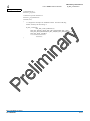
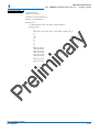
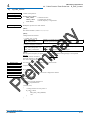
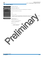
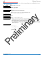
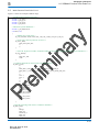
1. Introduction
The Renesas Peripheral Driver Library (PDL) is a unified API for controlling the peripheral modules on the microcontrollers
made by Renesas Technology.
User application
Callback functions
Peripheral Driver Library
CPU
Peripherals supported by the PDL
Target MCU
Figure 1-1: System configuration, with all peripherals supported by PDL
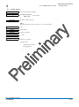
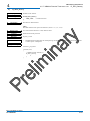
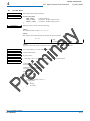
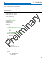
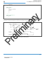
User application
Callback functions
Peripheral Driver Library
CPU
Middleware, including drivers
Peripherals supported by the PDL
USB, Ethernet or CAN
Target MCU
Figure 1-2: System configuration, with middleware taking direct control of some peripherals
The library is packaged as:
a) A binary file containing all of the peripheral driver functions and
b) Header files containing the information that the user needs to call any of the functions from their own application
code.
The binary file is produced using the Renesas SuperH Standard Tool chain v9.3. It should be usable by another compiler that
conforms to the Renesas Application Binary Interface.
The coding standards and naming conventions are specified by Renesas.
Rev.1.00 May 22 2012
YRSPSH7267-0103
1-1
1.1.
Using the library within your project
The driver library can be used:
1.
Via the PDG graphical utility
PDG can be downloaded from www.renesas.com/pdg.
The directions for use of the PDG utility are given in the PDG manual.
2.
Added to a project by the user and used stand-alone.
To add the driver library to your project’s build environment, you need to
a) Copy the required header and library files to a suitable location.
b) Include the required header files.
c) Add the driver library file to the linked files list.
1.1.1.
Copy the files
Copy the files to a suitable area using the Copy_PDL_SH7267_144_pin.bat utility.
1.1.2.
Include the header files
The header files are made available by adding an entry to their location.
From the Build menu, select “SuperH Standard engine Standard tool chain”.
From the C/C++ tab, open the “Show entries for :” drop-down menu and select “Include file directories”.
Click on the “Add…” button. From the “Relative to” drop-down list, select “Custom directory”.
Click on the “Browse…” button and navigate to the area where the files were copied.
Open the folder and click on “Select”.
Click on “OK”.
1.1.3.
Add the library file path
The library file is added to the list used by the linker application.
From the Link/Library tab, open the “Show entries for :” drop-down menu and select “Library files”.
Use the “Add…” button to add an entry for the PDL library.
1.1.4.
Build the project
No further configuration is required
Simply add the required PDL function calls to your source code, include the necessary header files and re-build the project.
1.2.
Document structure
The drivers are summarised in section 2 and explained in detail in section 4.
Section 5 provides comprehensive usage examples.
Section 6 provides details which are specific to the SuperH CPU.
Rev.1.00 May 22 2012
YRSPSH7267-0103
1-2
1.3.
Acronyms and abbreviations
ADC
API
Bit
BSC
CMT
CPG
CPU
DMA
DMAC
INTC
I/O
MCU
MTU2
NMI
PDG
PDL
PFC
SCIF
Analog to Digital Converter
Application Programming Interface
Binary digit
Bus State Controller
Compare Match Timer
Clock Pulse Generator
Central Processing Unit
Direct Memory Access
DMA Controller
Interrupt Controller
Input / Output
Microcontroller Unit
Multi Function Timer Pulse Unit 2
Non-Maskable Interrupt
Peripheral Driver Generator
Peripheral Driver Library
Port Function Control
Serial Communications Interface
Rev.1.00 May 22 2012
YRSPSH7267-0103
1-3
Driver
2
2.1 Overview
2. Driver
2.1.
Overview
This library provides a set of peripheral function control programs (peripheral drivers) for Renesas microcontrollers
and allows the peripheral driver to be built into a user program.
2.2.
Control Function
This library has the following control functions available as a peripheral driver.
(1) Serial Communication Interface
These driver functions are used to configure the serial channels and manage the transmission and / or reception of
data across them.
(2) I/O Port
These driver functions are used to configure the I/O pins and provide data read, write, compare and modify
operations.
(3) Port Function
These driver functions are used for configuring the I/O pin optional functions.
(4) Interrupt
These driver functions are used for configuring the external interrupt pins, handling fixed interrupts and controlling
the interrupt priority.
(5) Analog to Digital Converter
These driver functions are used for configuring the ADC units, controlling the units and reading the conversion
results.
(6) Clock Pulse Generator
These driver functions are used to configure the various internal/external clock signals.
(7) Compare Match Timer
These driver functions are used for configuring and controlling the timers.
(8) Multi Function Timer Pulse Unit 2
These driver functions are used for configuring and controlling the timers.
(9) Bus Controller
These driver functions are used for configuring the external address bus, data bus and chip select pins and handling
any bus errors.
(10) DMA Controller
These driver functions are used for configuring and controlling the transfer of data within the address space
Rev.1.00 May 22 2012
REJ09B0566
2-1
Driver
2.
2.3.
2.2 8BControl Function
Serial Communication Interface Driver
The driver functions support the use of the eight serial communication channels, providing the following
operations.
1. Configuration for use, including
a. Automatic baud rate clock calculations
b. Automatic interrupt control
c. Automatic I/O pin configuration
2. Disabling channels that are no longer required and enabling low-power mode.
3. Transmitting data, with polling or interrupt mode automatically selected.
4. Receiving data, with polling or interrupt mode automatically selected.
5. Stopping the transmission and / or reception of data.
6. Reading the status flags.
Rev.1.00 May 22 2012
REJ09B0566
2-2
Driver
2.
2.4.
2.2 8BControl Function
I/O Port Driver
The driver functions support the use of the 115 I/O port pins, providing the following operations.
1.
Configuration for use.
2.
Reading a pin or 16-bit port value.
3.
Writing to a pin or 16-bit port.
4.
Comparing a pin or 16-bit port with a supplied value.
5.
Modifying a pin or 16-bit port using a logical operation.
6.
Waiting until a pin or 16-bit port matches a supplied value.
Rev.1.00 May 22 2012
REJ09B0566
2-3
Driver
2.
2.5.
2.2 8BControl Function
Port Function Control Driver
The driver functions support access to the Port Function Control (PFC) registers which select the mode of operation
for some I/O pins.
The other driver functions modify the PFC registers automatically. For peripherals that are not supported by the
driver library, these functions support:
1. Reading from a PFC register.
2. Writing to a PFC register.
Rev.1.00 May 22 2012
REJ09B0566
2-4
Driver
2.
2.6.
2.2 8BControl Function
Interrupt Control Driver
The driver functions support the use of the interrupt controller, providing the following operations.
1. Configuration an external interrupt pin for use.
2. Controlling an external interrupt input.
3. Reading the status of an external interrupt.
4. Assigning handlers for the fixed exception interrupts.
5. Reading the current CPU interrupt priority level.
6. Changing the CPU interrupt priority level.
Rev.1.00 May 22 2012
REJ09B0566
2-5
Driver
2.
2.7.
2.2 8BControl Function
Analog to Digital Converter Driver
The driver functions support the use of the 8 ADC channels, providing the following operations.
1.
Configuration for use, including
a. Automatic clock setting using sampling time as an input.
b. Automatic interrupt control
c. Automatic I/O pin configuration
2.
Disabling units that are no longer required and enabling low-power mode.
3.
Control of one or more channels (depending upon the selected mode)
4.
Reading the conversion results of one of more units, with support for polling or interrupts.
Rev.1.00 May 22 2012
REJ09B0566
2-6
Driver
2.
2.8.
2.2 8BControl Function
Clock Pulse Generator Driver
The driver functions support the control of the internal clock generator, providing the following operations.
1.
Configuration of the multiple clock outputs for system, peripheral and external bus operation
2.
Controlling the bus clock output pin.
Rev.1.00 May 22 2012
REJ09B0566
2-7
Driver
2.
2.9.
2.2 8BControl Function
Compare Match Timer Driver
The driver functions support the use of the two 16-bit timers, providing the following operations.
1.
Configuration for use, including
a. Automatic clock setting using frequency or period as an input.
b. Automatic interrupt control
2.
Disabling channels that are no longer required and enabling low-power mode.
3.
Control of a timer, including change of frequency.
Rev.1.00 May 22 2012
REJ09B0566
2-8
Driver
2.
2.2 8BControl Function
2.10. Multi Function Timer Pulse Unit 2 Driver
The driver functions support the use of the five MTU2 channels, providing the following operations.
1.
Configuration for use, including
a. Access to all control bits.
b. Automatic interrupt control
c. Automatic I/O pin configuration
2.
Disabling channels that are no longer required and enabling low-power mode.
3.
Control of a timer.
4.
Reading the status and registers of a timer.
Rev.1.00 May 22 2012
REJ09B0566
2-9
Driver
2.
2.2 8BControl Function
2.11. Bus State Controller Driver
The driver functions support the control of the external bus, providing the following operations.
1. Configuration of the seven address space areas
2. Configuration of the error handling functions.
3. Disabling an area that is not required.
Rev.1.00 May 22 2012
REJ09B0566
2-10
Driver
2.
2.2 8BControl Function
2.12. DMA Controller Driver
The driver functions support the control of the Direct Memory Access (DMA) controller, providing the following
operations.
1. Configuration for use, including
a. Access to all control bits.
b. Automatic interrupt control
2. Disabling DMA channels that are no longer required and enabling low-power mode.
3. Control of one or more channels.
4. Reading the status and operation registers of a channel.
Rev.1.00 May 22 2012
REJ09B0566
2-11
3
Standard Type
3. Standard Types
This chapter describes the data types used in this library. For details about the setting values, refer to the section
“4.2 Description of Each API”.
Table 1: Data types
Type
bool
float
uint8_t
uint16_t
uint32_t
Defined in
typdefine.h
C
typedefine.h
Rev.1.00 May 22 2012
REJ09B0566
Description
Boolean
Floating point, 32 bits
Unsigned, 8 bits
Unsigned, 16 bits
Unsigned, 32 bits
Range
0 (false) to 1 (true)
-∞ to +∞
0 to 255
0 to 215-1
0 to 232-1
Library Reference
4
4
4.2 Description of Each API
4.1 API List by Peripheral Function
4. Library Reference
4.1.
API List by Peripheral Function
Table 4.1 lists the Renesas Embedded APIs by peripheral function.
Table 4.1 Renesas Embedded API List
Category
Clock Pulse Generator
Interrupt controller
I/O port
Port Function Control
Bus Controller
DMA Controller
Multi functional Timer
Unit
Compare Match Timer
Serial Communication
Interface
10-bit Analog to
Digital converter
Rev.1.00 May 22 2012
REJ09B0566
Number
1
1
2
3
4
5
6
7
1
2
3
4
5
6
7
8
1
2
3
1
2
3
4
5
1
2
3
4
1
2
3
4
1
2
3
4
1
2
3
4
5
6
1
2
3
4
Name
R_CPG_Set
R_INTC_CreateExtInterrupt
R_INTC_CreateExceptionHandlers
R_INTC_ControlExtInterrupt
R_INTC_GetExtInterruptStatus
R_INTC_Read
R_INTC_Write
R_INTC_Modify
R_IO_PORT_Set
R_IO_PORT_Read
R_IO_PORT_ReadControl
R_IO_PORT_Write
R_IO_PORT_Compare
R_IO_PORT_Modify
R_IO_PORT_ModifyControl
R_IO_PORT_Wait
R_PFC_Read
R_PFC_Write
R_PFC_Modify
R_BSC_Create
R_BSC_CreateArea
R_BSC_Destroy
R_BSC_Control
R_BSC_GetStatus
R_DMAC_Create
R_DMAC_Destroy
R_DMAC_Control
R_DMAC_GetStatus
R_MTU_Create
R_MTU_Destroy
R_MTU_Control
R_MTU_Read
R_CMT_Create
R_CMT_Destroy
R_CMT_Control
R_CMT_Read
R_SCI_Create
R_SCI_Destroy
R_SCI_Send
R_SCI_Receive
R_SCI_Stop
R_SCI_GetStatus
R_ADC_10_Create
R_CMT_Destroy
R_ADC_10_Control
R_ADC_10_Read
Description
Configure the clock pulse generator
Configure an external interrupt pin.
Enable faster interrupt processing for one interrupt.
External interrupt control.
Read the external interrupt status.
Read an interrupt register.
Update an interrupt register.
Modify an interrupt register.
Configure an I/O port.
Read an I/O port’s control registers.
Read an I/O port’s control registers.
Write an I/O port’s control registers.
Compare specified data with the data from an I/O port.
Modify the pin states on an I/O port.
Modify an I/O port’s control registers.
Wait for a match on an I/O port.
Read a PFC register.
Write to a PFC register.
Modify a PFC register.
Configure the external bus controller.
Configure an external bus area.
Stop the Bus Controller.
Modify the External Bus Controller operation.
Read the External Bus Controller status flags.
Configure the DMA controller.
Disable a DMA channel.
Control the DMA controller.
Check the status of the DMA channel.
Configure a Multi Functional Timer Unit channel.
Shut down a timer pulse unit.
Control a timer channel.
Read from timer channel registers.
Configure a CMT channel.
Disable a CMT unit.
Control CMT operation.
Read CMT channel status and registers.
SCI channel setup.
Shut down a SCI channel.
Send a string of characters.
Receive a string of characters.
Terminate SCI transmission or reception.
Check the status of a SCI channel.
Configure an ADC unit.
Disable the specified ADC unit.
Start or stop an ADC unit.
Read the ADC conversion results.
4-1
Library Reference
4
4.2 Description of Each API
4.2.
Description of Each API
This section describes each API and explains how to use them, showing a program example for each. The
description of each API is divided into the following items.
Synopsis
Prototype
Description
Return value
Summarises processing by the API function.
The function format and a brief explanation of the arguments.
Explains how to use the API function and shows assignable parameters separating each
argument with [argument].
Describes the returned value of the API function.
Category
Indicates the category of the API function.
Reference
Indicates the API functions to be referred.
Remark
Program example
Describes notes to use the API function.
Represents how to use the API function by a program example.
Two examples of return value checking are shown below.
/* PDL definitions */
#include “r_pdl_pfc.h”
#include “r_pdl_sci.h”
/* PDL device-specific definitions */
#include “r_pdl_definitions.h”
/* Application-specific definitions */
#include <stddef.h>
void func( void )
{
bool result;
/* Write 0xFF to register PFC1 */
result = (R_PFC_Write(
1,
0xFF
);
if (result == false)
{
/* Handle the error here */
}
/* Keep trying to send a string (if the channel is busy) */
do
{
result = R_SCISendString(
2,
“Renesas RX”,
NULL,
PDL_NO_FUNC
);
} while (result == false);
)
For clarity, the return value is not checked in the examples used in this manual.
Rev.1.00 May 22 2012
REJ09B0566
4-2
Library Reference
4
4.2.1
4.2.1.
1)
32BClock Pulse Generator
R_CPG_Set
Clock Pulse Generator
R_CPG_Set
Synopsis
Configure the clock pulse generator
Prototype
bool R_CPG_Set (
uint32_t data1,
// Input frequency uint32_t
data2,
// System clock frequency uint32_t
data3,
// Peripheral clock frequency uint8_t
data4,
// Clock mode settings uint8_t data5
// Configuration options
);
Description
Set the clock output frequencies and options.
[data1]
The frequency of the main clock oscillator in Hertz.
[data2]
The desired frequency of the System clock (ICLK) in Hertz.
[data3]
The desired frequency of the Peripheral clock (PCLK) in Hertz.
[data4]
Select the clock source
To select the Clock Source,
PDL_CPG_CK_0
PDL_CPG_USB_EXT
Specifies the clock operating mode (Mode 0 to 3)
PDL_CPG_CK_2
PDL_CPG_USB_PLL
Note: The default setting is shown in bold.
[data5]
Configuration options.
• BCLK pin output control
PDL_CPG_OUT_CK_00
PDL_CPG_OUT_CK_01
PDL_CPG_OUT_CK_02
PDL_CPG_OUT_CK_HIZ
Select whether to enable or disable the CKIO output
PDL_CPG_CK2_ENABLE
Enables or disables CKOEN2 bit in FRQCR register
PDL_CPG_CK2_DISABLE
Note: The default setting is shown in bold.
Return value
True if all parameters are valid and exclusive; otherwise false.
For SH7267, the following rules shall be checked:
• Main clock oscillator frequency: 10 to 18 MHz.
•
fICLK: 40 to 144 MHz
•
fPCLK: 6.7 to 36 MHz
•
fBCLK: 40 to 72 MHz
•
fICLK ≥ fPCLK and fICLK ≥ fBCLK
Functionality
Clock pulse generator
References
Remarks
Rev.1.00 May 22 2012
REJ09B0566
None.
•
•
This function must be called before configuring clock-dependent modules.
This function modifies the BCLK pin for input or output.
4-3
Library Reference
4
4.2.1
32BClock Pulse Generator
R_CPG_Set
Program example
/* PDL definitions */
#include “r_pdl_cpg.h”
/* PDL device-specific definitions */
#include “r_pdl_definitions.h”
void func(void)
{
/* Configure operation using a 18 MHz input clock */
/* ICLK = 144 MHz, PCLK = 36 MHz, BCLK = 72 MHz */
R_CPG_Set (18E6, 144E6, 36E6, PDL_CPG_CK_2, PDL_CPG_OUT_CK_01);
}
Rev.1.00 May 22 2012
REJ09B0566
4-4
Library Reference
4
4.2.2 33BInterrupt Control Unit R_INTC_CreateExtInterrupt
4.2.2.
1)
Interrupt Control Unit
R_INTC_CreateExtInterrupt
Synopsis
Configure an external interrupt pin.
Prototype
bool R_INTC_CreateExtInterrupt(
uint8_t data1,
// Interrupt selection
uint16_t data2,
// Configuration
uint8_t data3,
// Interrupt priority level
// Callback function
void * func
);
Description
Sets the specified external interrupt.
[data1]
Choose the interrupt pin to be configured.
PDL_INTC_IRQ0
PDL_INTC_IRQ1
PDL_INTC_IRQ2
PDL_INTC_IRQ3
PDL_INTC_IRQ4
PDL_INTC_IRQ5
PDL_INTC_IRQ6
PDL_INTC_IRQ7
PDL_INTC_PINT0
PDL_INTC_PINT1
PDL_INTC_PINT2
PDL_INTC_PINT3
PDL_INTC_PINT4
PDL_INTC_PINT5
PDL_INTC_PINT6
PDL_INTC_PINT7
PDL_INTC_NMI
PDL_INTC_GEN_ILL_INSTRUCTION
PDL_INTC_SLOT_ILL_INSTRUCTION
PDL_INTC_CPU_ADDR_ERR
PDL_INTC_DMA_ADDR_ERR
PDL_INTC_FPU
PDL_INTC_BANK_OVERFLOW
PDL_INTC_BANK_UNDERFLOW
PDL_INTC_DIV_BY_ZERO
PDL_INTC_DIV_OVERFLOW
External interrupt 0
External interrupt 1
External interrupt 2
External interrupt 3
External interrupt 4
External interrupt 5
External interrupt 6
External interrupt 7
External interrupt Pin 0
External interrupt Pin 1
External interrupt Pin 2
External interrupt Pin 3
External interrupt Pin 4
External interrupt Pin 5
External interrupt Pin 6
External interrupt Pin 7
NMI Interrupt
General illegal instruction
Slot illegal instruction
CPU Address Error
DMA Address Error
FPU Error
BANK Overflow Error
BANK Underflow Error
Divide by Zero Error
Divide Overflow Error
[data2]
Choose the pin settings. If multiple selections are required, use “|” to separate each selection.
The default settings are shown in bold.
• Detection sense selection (for the IRQ pins)
PDL_INTC_IRQ_LOW or
Select Low level,
PDL_INTC_IRQ_FALLING or
Falling edge,
PDL_INTC_IRQ_RISING or
Rising edge or
PDL_INTC_IRQ_BOTH
Falling and rising edge detection.
• Detection sense selection (for the PINT pin)
Select between PINT Low and High Level Selection.
PDL_INTC_PINT_LOW
PDL_INTC_PINT_HIGH
• Detection sense selection (for the NMI pin)
PDL_INTC_IRQ_FALLING or
Falling or rising edge detection.
PDL_INTC_IRQ_RISING
• Alternate pin selection (for the IRQ pins)
PDL_INTC_A or
Select the IRQn-A or IRQn-B pin to be used.
PDL_INTC_B
Rev.1.00 May 22 2012
REJ09B0566
4-5
Library Reference
4
4.2.2 33BInterrupt Control Unit R_INTC_CreateExtInterrupt
[func]
The function to be called when a valid condition is detected.
Specify PDL_NA if no IRQn interrupt is required.
A function must be specified for the NMI pin.
[data3]
The IRQn interrupt priority level. Select between 0 (interrupt disabled) and 15 (highest priority).
This value does not apply to the NMI pin and is ignored.
Return value
True if all parameters are valid and exclusive; otherwise false.
Category
External interrupt
Reference
R_INTC_ControlExtInterrupt, R_INTC_GetExtInterruptStatus
Remarks (1/2)
Rev.1.00 May 22 2012
REJ09B0566
• The selected interrupt pin is automatically enabled.
• I/O port register is modified to select the IRQn pin. The appropriate I/O port ICR register is modified to
enable the input buffer for that pin.
4-6
Library Reference
4
4.2.2 33BInterrupt Control Unit R_INTC_CreateExtInterrupt
Remarks (2/2)
• Please see the notes on callback function use
• The NMI callback function should not return. It should stop operation or reset the system.
Program example
#include “r_pdl_intc.h”
/* Declaration of callback function */
void CallBackFunc( void );
void func( void )
{
/* Configure the IRQ0 interrupt on pin IRQ1-A */
R_INTC_CreateExtInterrupt(
PDL_INTC_IRQ1,
PDL_INTC_IRQ_FALLING |
7,
CallBackFunc
);
}
Rev.1.00 May 22 2012
REJ09B0566
PDL_INTC_A,
4-7
Library Reference
4
2)
4.2.2 33BInterrupt Control Unit R_INTC_CreateExceptionHandlers
R_INTC_CreateExceptionHandlers
Synopsis
Assign handlers for the fixed-vector interrupts.
Prototype
bool R_INTC_CreateExceptionHandlers(
// Array of Callback function
void (* func())[9],
);
Description
Register the user functions to be called by the fixed-vector interrupts.
[(*func())[9]]
Array Function pointer containing callback function for all exception
Return value
True if all parameters are valid and exclusive; otherwise false.
Category
Interrupt control
Reference
R_INTC_CreateExtInterrupt
Remarks
• Please see the notes on callback function use
• A callback function is executed by the interrupt processing function. This means that no other interrupt
can be processed until the callback function has completed.
Program example
#include "r_pdl_intc.h"
/* Declaration of callback function */
Void callbackfunc1 (void);
Void callbackfunc2 (void);
Void callbackfunc3 (void);
Void callbackfunc4 (void);
Void callbackfunc5 (void);
Void callbackfunc6 (void);
Void callbackfunc7 (void);
Void callbackfunc8 (void);
Void callbackfunc9 (void);
void (*CallBackFunc( void ))[9] = { callbackfunc1,
callbackfunc2,callbackfunc3,callbackfunc4,
callbackfunc5,callbackfunc6,callbackfunc7,
callbackfunc8,callbackfunc9
};
void func( void )
{
/* Add a function to manage floating point errors */
R_INTC_CreateExceptionHandlers(CallBackFunc);
}
Rev.1.00 May 22 2012
REJ09B0566
4-8
Library Reference
4
3)
4.2.2 33BInterrupt Control Unit
R_INTC_ControlExtInterrupt
R_INTC_ControlExtInterrupt
Synopsis
External interrupt control.
Prototype
bool R_INTC_ControlExtInterrupt(
uint8_t data1,
// Pin selection
uint16_t data2
// Control
);
Description
Enables or disables the specified external interrupt.
[data1]
Choose the interrupt pin to be configured.
PDL_INTC_IRQ0
PDL_INTC_IRQ1
PDL_INTC_IRQ2
PDL_INTC_IRQ3
PDL_INTC_IRQ4
PDL_INTC_IRQ5
PDL_INTC_IRQ6
PDL_INTC_IRQ7
PDL_INTC_PINT0
PDL_INTC_PINT1
PDL_INTC_PINT2
PDL_INTC_PINT3
PDL_INTC_PINT4
PDL_INTC_PINT5
PDL_INTC_PINT6
PDL_INTC_PINT7
PDL_INTC_NMI
PDL_INTC_GEN_ILL_INSTRUCTION
PDL_INTC_SLOT_ILL_INSTRUCTION
PDL_INTC_CPU_ADDR_ERR
PDL_INTC_DMA_ADDR_ERR
PDL_INTC_FPU
PDL_INTC_BANK_OVERFLOW
PDL_INTC_BANK_UNDERFLOW
PDL_INTC_DIV_BY_ZERO
PDL_INTC_DIV_OVERFLOW
External interrupt 0
External interrupt 1
External interrupt 2
External interrupt 3
External interrupt 4
External interrupt 5
External interrupt 6
External interrupt 7
External interrupt Pin 0
External interrupt Pin 1
External interrupt Pin 2
External interrupt Pin 3
External interrupt Pin 4
External interrupt Pin 5
External interrupt Pin 6
External interrupt Pin 7
NMI Interrupt
General illegal instruction
Slot illegal instruction
CPU Address Error
DMA Address Error
FPU Error
BANK Overflow Error
BANK Underflow Error
Divide by Zero Error
Divide Overflow Error
[data2]
Select the controls. If multiple selections are required, use “|” to separate each selection.
• Enable or disable the interrupt pin (for the IRQ pins)
PDL_INTC_ENABLE or
Enable or disable the IRQn interrupt pin.
PDL_INTC_DISABLE
• Detection sense selection (for the IRQ pins)
PDL_INTC_IRQ_LOW or
Low level detection
PDL_INTC_IRQ_FALLING or
Falling edge detection
PDL_INTC_IRQ_RISING or
Rising edge detection
PDL_INTC_IRQ_BOTH
Falling and rising edge detection
• Enable or disable the interrupt pin (for the PINTIRQ pins)
PDL_INTC_PINT_LOW
Select between PINT Low or High Level Selection
PDL_INTC_PINT_HIGH
Return value
True if all parameters are valid and exclusive; otherwise false.
Category
External interrupt
Reference
R_INTC_CreateExtInterrupt, R_INTC_GetExtInterruptStatus
Rev.1.00 May 22 2012
REJ09B0566
4-9
Library Reference
4
4.2.2 33BInterrupt Control Unit
Remarks
Rev.1.00 May 22 2012
REJ09B0566
R_INTC_ControlExtInterrupt
• The NMI pin was enabled during R_INTC_CreateExtInterrupt and cannot be disabled (an MCU design
feature).
• When disabling an IRQn pin, the Interrupt Request flag will be cleared automatically.
A callback function may be called once more if a valid event occurs just before the interrupt pin is
disabled.
4-10
Library Reference
4
4.2.2 33BInterrupt Control Unit
R_INTC_ControlExtInterrupt
Program example
#include "r_pdl_intc.h"
void func( void )
{
/* Disable the IRQ1 interrupt pin and clear the flag */
R_INTC_ControlExtInterrupt(
PDL_INTC_IRQ1,
PDL_INTC_R_INTC_DISABLE
);
}
Rev.1.00 May 22 2012
REJ09B0566
4-11
Library Reference
4
4)
4.2.2
R_INTC_GetExtInterruptStatus
33BInterrupt Control Unit
R_INTC_GetExtInterruptStatus
Synopsis
Read the external interrupt status.
Prototype
bool R_INTC_GetExtInterruptStatus(
uint8_t data1,
// Pin selection
// A pointer to the buffer where the status data shall be stored.
uint8_t * data2
);
Description
Acquire the status for the specified external interrupt.
[data1]
Choose the interrupt pin to be checked.
PDL_INTC_IRQ0
PDL_INTC_IRQ1
PDL_INTC_IRQ2
PDL_INTC_IRQ3
PDL_INTC_IRQ4
PDL_INTC_IRQ5
PDL_INTC_IRQ6
PDL_INTC_IRQ7
PDL_INTC_PINT0
PDL_INTC_PINT1
PDL_INTC_PINT2
PDL_INTC_PINT3
PDL_INTC_PINT4
PDL_INTC_PINT5
PDL_INTC_PINT6
PDL_INTC_PINT7
PDL_INTC_NMI
PDL_INTC_GEN_ILL_INSTRUCTI
ON
PDL_INTC_SLOT_ILL_INSTRUCTI
ON
PDL_INTC_CPU_ADDR_ERR
PDL_INTC_DMA_ADDR_ERR
PDL_INTC_FPU
PDL_INTC_BANK_OVERFLOW
PDL_INTC_BANK_UNDERFLOW
PDL_INTC_DIV_BY_ZERO
PDL_INTC_DIV_OVERFLOW
External interrupt 0
External interrupt 1
External interrupt 2
External interrupt 3
External interrupt 4
External interrupt 5
External interrupt 6
External interrupt 7
External interrupt Pin 0
External interrupt Pin 1
External interrupt Pin 2
External interrupt Pin 3
External interrupt Pin 4
External interrupt Pin 5
External interrupt Pin 6
External interrupt Pin 7
NMI Interrupt
General illegal instruction
Slot illegal instruction
CPU Address Error
DMA Address Error
FPU Error
BANK Overflow Error
BANK Underflow Error
Divide by Zero Error
Divide Overflow Error
[data2]
The status flags shall be stored in the following format:
For an IRQ and PINT pin:
b7 – b4
b3 – b2
00: Low level detection
01: Falling edge detection
10: Rising edge detection
11: Both edge detection
For the NMI pin:
b7 – b2
Return value
b1
Pin logic
level
b1
0: Falling edge detection
1: Rising edge detection
0: Idle
1: Valid interrupt condition detected
b0
0: Idle
1: Valid interrupt condition detected
True if all parameters are valid and exclusive; otherwise false.
Category
External interrupt
Reference
R_INTC_CreateExtInterrupt, R_INTC_ControlExtInterrupt
Remarks
• None
Rev.1.00 May 22 2012
REJ09B0566
b0
4-12
4
Library Reference
4.2.2
33BInterrupt Control Unit
R_INTC_GetExtInterruptStatus
Program example
#include "r_pdl_intc.h"
void func( void )
{
uint8_t irq_status;
/* Read the IR flags and pin states for IRQ5 */
R_INTC_GetExtInterruptStatus(
PDL_INTC_IRQ5,
&irq_status
);
}
Rev.1.00 May 22 2012
REJ09B0566
4-13
Library Reference
4
5)
4.2.2 33BInterrupt Control Unit
R_INTC_Read
R_INTC_Read
Synopsis
Read an interrupt register.
Prototype
bool R_INTC_Read(
uint8_t data1,
uint8_t data2,
uint8_t * data3
);
Description
// Register selection
// Register number
// Data storage location
Read an interrupt register and store the value.
[data1]
• The register to be read
PDL_INTC_REG_ICR or
PDL_INTC_REG_IPR or
PDL_INTC_REG_IRQRR or
PDL_INTC_REG_PIRR or
PDL_INTC_REG_PINTER or
PDL_INTC_REG_IBNR or
PDL_INTC_REG_IBCR
Select the current CPU interrupt priority level or
IRQ Control Register
IRQ Priority Register
IRQ Interrupt Request Register
PINT Interrupt Enable Register
PINT Interrupt Request Register
Bank Control Register
Bank Number Register
[data2]
The register number.
ICR: Between 0 and 3
IPR: Between 0 and 22 (16h).
IRQRR: Ignored.
PIRR: Ignored.
PINTER: Ignored.
IBCR: Ignored.
IBCR: Ignored.
[data3]
The location where the register’s value shall be stored.
Return value
True.
Category
Interrupt control
Reference
R_INTC_Write, R_INTC_Modify
Remarks
• None.
Program example
/* PDL definitions */
#include “r_pdl_intc.h”
/* PDL device-specific definitions */
#include “r_pdl_definitions.h”
void func( void )
{
uint8_t ipl;
/* Read the IPL bits */
R_INTC_Read(
PDL_INTC_REG_IPL,
0,
&ipl
);
}
Rev.1.00 May 22 2012
REJ09B0566
4-14
Library Reference
4
6)
4.2.2 33BInterrupt Control Unit
R_INTC_Write
R_INTC_Write
Synopsis
Update an interrupt register.
Prototype
bool R_INTC_Write(
uint8_t data1,
// Register selection
uint8_t data2,
// Register number
uint8_t data3
// Register value
);
Description
Write the new value to an interrupt register.
[data1]
• The register to be updated.
PDL_INTC_REG_ICR or
PDL_INTC_REG_IPR or
PDL_INTC_REG_IRQRR or
PDL_INTC_REG_PIRR or
PDL_INTC_REG_PINTER or
PDL_INTC_REG_IBNR or
PDL_INTC_REG_IBCR
Select the current CPU interrupt priority level or
IRQ Control Register
IRQ Priority Register
IRQ Interrupt Request Register
PINT Interrupt Enable Register
PINT Interrupt Request Register
Bank Control Register
Bank Number Register
[data2]
The register number.
ICR: Between 0 and 3
IPR: Between 0 and 22 (16h).
IRQRR: Ignored.
PIRR: Ignored.
PINTER: Ignored.
IBCR: Ignored.
IBCR: Ignored.
[data3]
The value to be written to the register.
Return value
True if the parameter is within range; otherwise false.
Category
Interrupt control
Reference
R_INTC_Read, R_INTC_Modify
Remarks
• This function uses an interrupt routine to modify the IPL bits. If the user has disabled interrupts (cleared
the ‘I’ bit in the PSW register) in their own code, this function will lock up.
Program example
/* PDL definitions */
#include “r_pdl_intc.h”
/* PDL device-specific definitions */
#include “r_pdl_definitions.h”
void func( void )
{
/* Set the IPL to 6 */
R_INTC_Write(
PDL_INTC_REG_IPL,
0,
6
);
}
Rev.1.00 May 22 2012
REJ09B0566
4-15
Library Reference
4
7)
4.2.2 33BInterrupt Control Unit
R_INTC_Modify
R_INTC_Modify
Synopsis
Modify an interrupt register.
Prototype
bool R_INTC_Modify(
uint8_t data1,
// Register selection
uint8_t data2,
// number
uint8_t data3,
// Modification value
// Logical operation
uint8_t data4
);
Description
Write the new value to the IPL bits in the Processor Status Word register.
[data1]
• The register to be updated.
PDL_INTC_REG_ICR or
PDL_INTC_REG_IPR or
PDL_INTC_REG_IRQRR or
PDL_INTC_REG_PIRR or
PDL_INTC_REG_PINTER or
PDL_INTC_REG_IBNR or
PDL_INTC_REG_IBCR
Select the current CPU interrupt priority level or
IRQ Control Register
IRQ Priority Register
IRQ Interrupt Request Register
PINT Interrupt Enable Register
PINT Interrupt Request Register
Bank Control Register
Bank Number Register
[data2]
The register number.
ICR: Between 0 and 3
IPR: Between 0 and 22 (16h).
IRQRR: Ignored.
PIRR: Ignored.
PINTER: Ignored.
IBCR: Ignored.
IBCR: Ignored.
[data3]
The value to be used by the logical operation.
[data4]
• The logical operation to be applied to the register contents.
PDL_INTC_AND or
PDL_INTC_OR or
Select between AND (&), OR (|) or Exclusive-OR (^).
PDL_INTC_XOR
Return value
True if the parameter is within range; otherwise false.
Category
Interrupt control
Reference
R_INTC_Read, R_INTC_Write
Remarks
• This function uses an interrupt routine to modify the IPL bits. If the user has disabled interrupts (cleared
the ‘I’ bit in the PSW register) in their own code, this function will lock up.
Program example
Rev.1.00 May 22 2012
REJ09B0566
4-16
Library Reference
4
4.2.2 33BInterrupt Control Unit
R_INTC_Modify
/* PDL definitions */
#include “r_pdl_intc.h”
/* PDL device-specific definitions */
#include “r_pdl_definitions.h”
void func( void )
{
/* Set bits 6 and 4 in IER09 to 1 */
R_INTC_Modify(
PDL_INTC_REG_IER,
0x09,
0x50,
PDL_INTC_OR
);
}
Rev.1.00 May 22 2012
REJ09B0566
4-17
Library Reference
4
4.2.3 34BI/O Port
4.2.3.
1)
R_IO_PORT_Set
I/O Port
R_IO_PORT_Set
Synopsis
Configure an I/O port.
Prototype
bool R_IO_PORT_Set(
uint32_t data1,
// Port or port pin selection
uint16_t data2,
// Data direction value
// CMOS output to be controlled
uint16_t data3,
);
Description (1/3)
Sets the operating conditions of an I/O port or I/O port pin.
[data1]
Use either one of the following definition values to select the I/O port.
PDL_IO_PORT_A
PORT A
PDL_IO_PORT_F
PDL_IO_PORT_BH
PORT BH
PDL_IO_PORT_GH
PDL_IO_PORT_BL
PORT BL
PDL_IO_PORT_GL
PDL_IO_PORT_C
PORT C
PDL_IO_PORT_H
PDL_IO_PORT_D
PORT D
PDL_IO_PORT_I
PDL_IO_PORT_E
PORT E
PDL_IO_PORT_K
PORT F
PORT GH
PORT GL
PORT H
PORT I
PORT K
Or use any of the following definition values to select the I/O port pin.
Multiple pins on the same port may be specified, using “|” to separate each pin.
PDL_IO_PORT_A_0
PORT A0
PDL_IO_PORT_B_1
PORT B1
PDL_IO_PORT_A_1
PORT A1
PDL_IO_PORT_B_2
PORT B2
PDL_IO_PORT_A_2
PORT A2
PDL_IO_PORT_B_3
PORT B3
PDL_IO_PORT_A_3
PORT A3
PDL_IO_PORT_B_4
PORT B4
PDL_IO_PORT_C_0
PORT C0
PDL_IO_PORT_B_5
PORT B5
PDL_IO_PORT_C_1
PORT C1
PDL_IO_PORT_B_6
PORT B6
PDL_IO_PORT_C_2
PORT C2
PDL_IO_PORT_B_7
PORT B7
PDL_IO_PORT_C_3
PORT C3
PDL_IO_PORT_B_8
PORT B8
PDL_IO_PORT_C_4
PORT C4
PDL_IO_PORT_B_9
PORT B9
PDL_IO_PORT_C_5
PORT C5
PDL_IO_PORT_B_10 PORT B10
PDL_IO_PORT_C_6
PORT C6
PDL_IO_PORT_B_11 PORT B11
PDL_IO_PORT_C_7
PORT C7
PDL_IO_PORT_B_12 PORT B12
PDL_IO_PORT_C_8
PORT C8
PDL_IO_PORT_B_13 PORT B13
PDL_IO_PORT_C_9
PORT C9
PDL_IO_PORT_B_14 PORT B14
PDL_IO_PORT_C_10
PORT C10
PDL_IO_PORT_B_15 PORT B15
PDL_IO_PORT_D_0
PORT D0
PDL_IO_PORT_B_16 PORT B16
PDL_IO_PORT_D_1
PORT D1
PDL_IO_PORT_B_17 PORT B17
PDL_IO_PORT_D_2
PORT D2
PDL_IO_PORT_B_18 PORT B18
PDL_IO_PORT_D_3
PORT D3
PDL_IO_PORT_B_19 PORT B19
PDL_IO_PORT_D_4
PORT D4
PDL_IO_PORT_B_20 PORT B20
PDL_IO_PORT_D_5
PORT D5
PDL_IO_PORT_B_21 PORT B21
PDL_IO_PORT_D_6
PORT D6
PDL_IO_PORT_B_22 PORT B22
PDL_IO_PORT_D_7
PORT D7
PDL_IO_PORT_E_0
PORT E0
PDL_IO_PORT_D_8
PORT D8
PDL_IO_PORT_E_1
PORT E1
PDL_IO_PORT_D_9
PORT D9
PDL_IO_PORT_E_2
PORT E2
PDL_IO_PORT_D_10
PORT D10
PDL_IO_PORT_E_3
PORT E3
PDL_IO_PORT_D_11
PORT D11
PDL_IO_PORT_E_4
PORT E4
PDL_IO_PORT_D_12
PORT D12
PDL_IO_PORT_E_5
PORT E5
PDL_IO_PORT_D_13
PORT D13
PDL_IO_PORT_F_0
PORT F0
PDL_IO_PORT_D_14
PORT D14
PDL_IO_PORT_F_1
PORT F1
PDL_IO_PORT_D_15
PORT D15
PDL_IO_PORT_F_2
PORT F2
PDL_IO_PORT_G_0
PORT G0
PDL_IO_PORT_F_3
PORT F3
PDL_IO_PORT_G_1
PORT G1
PDL_IO_PORT_F_4
PORT F4
Rev.1.00 May 22 2012
REJ09B0566
4-18
Library Reference
4
4.2.3 34BI/O Port
PDL_IO_PORT_G_2
PDL_IO_PORT_G_3
PDL_IO_PORT_G_4
PDL_IO_PORT_G_5
PDL_IO_PORT_G_6
PDL_IO_PORT_G_7
PDL_IO_PORT_G_8
PDL_IO_PORT_G_9
PDL_IO_PORT_G_10
PDL_IO_PORT_G_11
PDL_IO_PORT_G_12
PDL_IO_PORT_G_13
PDL_IO_PORT_G_14
PDL_IO_PORT_G_15
PDL_IO_PORT_G_16
PDL_IO_PORT_G_17
PDL_IO_PORT_G_18
PDL_IO_PORT_G_19
PDL_IO_PORT_G_20
PDL_IO_PORT_G_21
PDL_IO_PORT_G_22
PDL_IO_PORT_G_23
PDL_IO_PORT_G_24
PDL_IO_PORT_K_0
PDL_IO_PORT_K_1
PDL_IO_PORT_K_2
PDL_IO_PORT_K_3
PDL_IO_PORT_K_4
PDL_IO_PORT_K_5
PDL_IO_PORT_K_6
PDL_IO_PORT_K_7
PDL_IO_PORT_K_8
PORT G2
PORT G3
PORT G4
PORT G5
PORT G6
PORT G7
PORT G8
PORT G9
PORT G10
PORT G11
PORT G12
PORT G13
PORT G14
PORT G15
PORT G16
PORT G17
PORT G18
PORT G19
PORT G20
PORT G21
PORT G22
PORT G23
PORT G24
PORT K0
PORT K1
PORT K2
PORT K3
PORT K4
PORT K5
PORT K6
PORT K7
PORT K8
R_IO_PORT_Set
PDL_IO_PORT_F_5
PDL_IO_PORT_F_6
PDL_IO_PORT_F_7
PDL_IO_PORT_F_8
PDL_IO_PORT_F_9
PDL_IO_PORT_F_10
PDL_IO_PORT_F_11
PDL_IO_PORT_F_12
PDL_IO_PORT_H_0
PDL_IO_PORT_H_1
PDL_IO_PORT_H_2
PDL_IO_PORT_H_3
PDL_IO_PORT_H_4
PDL_IO_PORT_H_5
PDL_IO_PORT_H_6
PDL_IO_PORT_H_7
PDL_IO_PORT_J_0
PDL_IO_PORT_J_1
PDL_IO_PORT_J_2
PDL_IO_PORT_J_3
PDL_IO_PORT_J_4
PDL_IO_PORT_J_5
PDL_IO_PORT_J_6
PDL_IO_PORT_J_7
PDL_IO_PORT_J_8
PDL_IO_PORT_J_9
PDL_IO_PORT_J_10
PDL_IO_PORT_J_11
PDL_IO_PORT_K_9
PDL_IO_PORT_K_10
PDL_IO_PORT_K_11
PORT F5
PORT F6
PORT F7
PORT F8
PORT F9
PORT F10
PORT F11
PORT F12
PORT H0
PORT H1
PORT H2
PORT H3
PORT H4
PORT H5
PORT H6
PORT H7
PORT J0
PORT J1
PORT J2
PORT J3
PORT J4
PORT J5
PORT J6
PORT J7
PORT J8
PORT J9
PORT J10
PORT J11
PORT K9
PORT K10
PORT K11
[data2]
Specify the value for the port’s data direction register.
For a port, provide a number between 0x00 and 0xFF.
b7
b6
b5
b4
b3
Pin Pn7
Pin Pn6
Pin Pn5
Pin Pn4
Pin Pn3
0: Input
1: Output
For a pin,
PDL_IO_PORT_INPUT or
PDL_IO_PORT_OUTPUT or
0
True if all parameters are valid and exclusive; otherwise false.
Functionality
I/O port
Remarks
Rev.1.00 May 22 2012
REJ09B0566
b1
Pin Pn1
b0
Pin Pn0
Input,
output or
leave unchanged.
Return value
References
b2
Pin Pn2
R_IO_PORT_Write, R_IO_PORT_Read
• Ensure that the specified functions are valid for the selected port pin.
• The data direction and input buffer registers are modified by other driver Create functions. Take care to
not overwrite existing settings.
4-19
Library Reference
4
4.2.3 34BI/O Port
R_IO_PORT_Set
Program example
/* PDL definitions */
#include “r_pdl_io_port.h”
/* PDL device-specific definitions */
#include “r_pdl_definitions.h”
void func(void)
{
/* Set the control registers for port D1 */
R_IO_PORT_Set(
PDL_IO_PORT_D,
0xAA,
0x00
);
/* Set up port PB03 as an input port */
R_IO_PORT_Set(
PDL_IO_PORT_B_3,
PDL_IO_PORT_INPUT,
0
);
}
Rev.1.00 May 22 2012
REJ09B0566
4-20
Library Reference
4
2)
4.2.3 34BI/O Port
R_IO_PORT_Read
R_IO_PORT_Read
Synopsis
Read data from an I/O port.
Prototype
bool R_IO_PORT_Read (
uint32_t data1,
// Port or port pin selection
uint16_t * data3 // Pointer to the variable in which the value shall be stored.
);
Description (1/2)
Gets the value of an I/O port or I/O port pin.
[data1]
Use either one of the following definition values to select the I/O port.
PDL_IO_PORT_A
PDL_IO_PORT_BH
PDL_IO_PORT_BL
PDL_IO_PORT_C
PDL_IO_PORT_D
PDL_IO_PORT_E
PORT A
PORT BH
PORT BL
PORT C
PORT D
PORT E
PDL_IO_PORT_F
PDL_IO_PORT_GH
PDL_IO_PORT_GL
PDL_IO_PORT_H
PDL_IO_PORT_I
PDL_IO_PORT_K
PORT F
PORT GH
PORT GL
PORT H
PORT I
PORT K
Or any of the following definition values to select the I/O port pin.
PDL_IO_PORT_A_0
PDL_IO_PORT_A_1
PDL_IO_PORT_A_2
PDL_IO_PORT_A_3
PDL_IO_PORT_C_0
PDL_IO_PORT_C_1
PDL_IO_PORT_C_2
PDL_IO_PORT_C_3
PDL_IO_PORT_C_4
PDL_IO_PORT_C_5
PDL_IO_PORT_C_6
PDL_IO_PORT_C_7
PDL_IO_PORT_C_8
PDL_IO_PORT_C_9
PDL_IO_PORT_C_10
PDL_IO_PORT_D_0
PDL_IO_PORT_D_1
PDL_IO_PORT_D_2
PDL_IO_PORT_D_3
PDL_IO_PORT_D_4
PDL_IO_PORT_D_5
PDL_IO_PORT_D_6
PDL_IO_PORT_D_7
PDL_IO_PORT_D_8
PDL_IO_PORT_D_9
PDL_IO_PORT_D_10
PDL_IO_PORT_D_11
PDL_IO_PORT_D_12
PDL_IO_PORT_D_13
PDL_IO_PORT_D_14
PDL_IO_PORT_D_15
PDL_IO_PORT_G_0
PDL_IO_PORT_G_1
PDL_IO_PORT_G_2
PDL_IO_PORT_G_3
PDL_IO_PORT_G_4
Rev.1.00 May 22 2012
REJ09B0566
PORT A0
PORT A1
PORT A2
PORT A3
PORT C0
PORT C1
PORT C2
PORT C3
PORT C4
PORT C5
PORT C6
PORT C7
PORT C8
PORT C9
PORT C10
PORT D0
PORT D1
PORT D2
PORT D3
PORT D4
PORT D5
PORT D6
PORT D7
PORT D8
PORT D9
PORT D10
PORT D11
PORT D12
PORT D13
PORT D14
PORT D15
PORT G0
PORT G1
PORT G2
PORT G3
PORT G4
PDL_IO_PORT_B_1
PDL_IO_PORT_B_2
PDL_IO_PORT_B_3
PDL_IO_PORT_B_4
PDL_IO_PORT_B_5
PDL_IO_PORT_B_6
PDL_IO_PORT_B_7
PDL_IO_PORT_B_8
PDL_IO_PORT_B_9
PDL_IO_PORT_B_10
PDL_IO_PORT_B_11
PDL_IO_PORT_B_12
PDL_IO_PORT_B_13
PDL_IO_PORT_B_14
PDL_IO_PORT_B_15
PDL_IO_PORT_B_16
PDL_IO_PORT_B_17
PDL_IO_PORT_B_18
PDL_IO_PORT_B_19
PDL_IO_PORT_B_20
PDL_IO_PORT_B_21
PDL_IO_PORT_B_22
PDL_IO_PORT_E_0
PDL_IO_PORT_E_1
PDL_IO_PORT_E_2
PDL_IO_PORT_E_3
PDL_IO_PORT_E_4
PDL_IO_PORT_E_5
PDL_IO_PORT_F_0
PDL_IO_PORT_F_1
PDL_IO_PORT_F_2
PDL_IO_PORT_F_3
PDL_IO_PORT_F_4
PDL_IO_PORT_F_5
PDL_IO_PORT_F_6
PDL_IO_PORT_F_7
PORT B1
PORT B2
PORT B3
PORT B4
PORT B5
PORT B6
PORT B7
PORT B8
PORT B9
PORT B10
PORT B11
PORT B12
PORT B13
PORT B14
PORT B15
PORT B16
PORT B17
PORT B18
PORT B19
PORT B20
PORT B21
PORT B22
PORT E0
PORT E1
PORT E2
PORT E3
PORT E4
PORT E5
PORT F0
PORT F1
PORT F2
PORT F3
PORT F4
PORT F5
PORT F6
PORT F7
4-21
Library Reference
4
4.2.3 34BI/O Port
PDL_IO_PORT_G_5
PDL_IO_PORT_G_6
PDL_IO_PORT_G_7
PDL_IO_PORT_G_8
PDL_IO_PORT_G_9
PDL_IO_PORT_G_10
PDL_IO_PORT_G_11
PDL_IO_PORT_G_12
PDL_IO_PORT_G_13
PDL_IO_PORT_G_14
PDL_IO_PORT_G_15
PDL_IO_PORT_G_16
PDL_IO_PORT_G_17
PDL_IO_PORT_G_18
PDL_IO_PORT_G_19
PDL_IO_PORT_G_20
PDL_IO_PORT_G_21
PDL_IO_PORT_G_22
PDL_IO_PORT_G_23
PDL_IO_PORT_G_24
PDL_IO_PORT_K_0
PDL_IO_PORT_K_1
PDL_IO_PORT_K_2
PDL_IO_PORT_K_3
PDL_IO_PORT_K_4
PDL_IO_PORT_K_5
PDL_IO_PORT_K_6
PDL_IO_PORT_K_7
PDL_IO_PORT_K_8
PORT G5
PORT G6
PORT G7
PORT G8
PORT G9
PORT G10
PORT G11
PORT G12
PORT G13
PORT G14
PORT G15
PORT G16
PORT G17
PORT G18
PORT G19
PORT G20
PORT G21
PORT G22
PORT G23
PORT G24
PORT K0
PORT K1
PORT K2
PORT K3
PORT K4
PORT K5
PORT K6
PORT K7
PORT K8
R_IO_PORT_Read
PDL_IO_PORT_F_8
PDL_IO_PORT_F_9
PDL_IO_PORT_F_10
PDL_IO_PORT_F_11
PDL_IO_PORT_F_12
PDL_IO_PORT_H_0
PDL_IO_PORT_H_1
PDL_IO_PORT_H_2
PDL_IO_PORT_H_3
PDL_IO_PORT_H_4
PDL_IO_PORT_H_5
PDL_IO_PORT_H_6
PDL_IO_PORT_H_7
PDL_IO_PORT_J_0
PDL_IO_PORT_J_1
PDL_IO_PORT_J_2
PDL_IO_PORT_J_3
PDL_IO_PORT_J_4
PDL_IO_PORT_J_5
PDL_IO_PORT_J_6
PDL_IO_PORT_J_7
PDL_IO_PORT_J_8
PDL_IO_PORT_J_9
PDL_IO_PORT_J_10
PDL_IO_PORT_J_11
PDL_IO_PORT_K_9
PDL_IO_PORT_K_10
PDL_IO_PORT_K_11
PORT F8
PORT F9
PORT F10
PORT F11
PORT F12
PORT H0
PORT H1
PORT H2
PORT H3
PORT H4
PORT H5
PORT H6
PORT H7
PORT J0
PORT J1
PORT J2
PORT J3
PORT J4
PORT J5
PORT J6
PORT J7
PORT J8
PORT J9
PORT J10
PORT J11
PORT K9
PORT K10
PORT K11
[data2]
The value will be between 0x0000 and 0xFFFF for a port, 0 or 1 for a pin.
Return value
If the I/O port specification is incorrect, false is returned; otherwise, true is returned.
Functionality
I/O port
Reference
Remark
Rev.1.00 May 22 2012
REJ09B0566
R_IO_PORT_Set
• If an invalid port or pin is specified, the operation of the function cannot be guaranteed.
4-22
Library Reference
4
4.2.3 34BI/O Port
R_IO_PORT_Read
Program example
#include "r_pdl_io_port.h"
void func( void )
{
uint16_t data;
/* Get the value of port E */
R_IO_PORT_Read(PDL_IO_PORT_E, &data);
/* Get the value of port F2 */
R_IO_PORT_Read(PDL_IO_PORT_F_2, &data);
}
Rev.1.00 May 22 2012
REJ09B0566
4-23
Library Reference
4
3)
4.2.3 34BI/O Port
R_IO_PORT_Write
R_IO_PORT_ReadControl
Synopsis
Read an I/O port’s control registers.
Prototype
bool R_IO_PORT_ReadControl (
uint32_t data1,
// Port or port pin selection
uint16_t * data3 // Pointer to the variable in which the data direction value shall be stored.
);
Description (1/2)
Gets the value of an I/O port or I/O port pin.
[data1]
Use either one of the following definition values to select the I/O port.
PDL_IO_PORT_A
PDL_IO_PORT_BH
PDL_IO_PORT_BL
PDL_IO_PORT_C
PDL_IO_PORT_D
PDL_IO_PORT_E
PORT A
PORT BH
PORT BL
PORT C
PORT D
PORT E
PDL_IO_PORT_F
PDL_IO_PORT_GH
PDL_IO_PORT_GL
PDL_IO_PORT_H
PDL_IO_PORT_I
PDL_IO_PORT_K
PORT F
PORT GH
PORT GL
PORT H
PORT I
PORT K
Or any of the following definition values to select the I/O port pin.
PDL_IO_PORT_A_0
PDL_IO_PORT_A_1
PDL_IO_PORT_A_2
PDL_IO_PORT_A_3
PDL_IO_PORT_C_0
PDL_IO_PORT_C_1
PDL_IO_PORT_C_2
PDL_IO_PORT_C_3
PDL_IO_PORT_C_4
PDL_IO_PORT_C_5
PDL_IO_PORT_C_6
PDL_IO_PORT_C_7
PDL_IO_PORT_C_8
PDL_IO_PORT_C_9
PDL_IO_PORT_C_10
PDL_IO_PORT_D_0
PDL_IO_PORT_D_1
PDL_IO_PORT_D_2
PDL_IO_PORT_D_3
PDL_IO_PORT_D_4
PDL_IO_PORT_D_5
PDL_IO_PORT_D_6
PDL_IO_PORT_D_7
PDL_IO_PORT_D_8
PDL_IO_PORT_D_9
PDL_IO_PORT_D_10
PDL_IO_PORT_D_11
PDL_IO_PORT_D_12
PDL_IO_PORT_D_13
PDL_IO_PORT_D_14
PDL_IO_PORT_D_15
PDL_IO_PORT_G_0
PDL_IO_PORT_G_1
PDL_IO_PORT_G_2
PDL_IO_PORT_G_3
PDL_IO_PORT_G_4
Rev.1.00 May 22 2012
REJ09B0566
PORT A0
PORT A1
PORT A2
PORT A3
PORT C0
PORT C1
PORT C2
PORT C3
PORT C4
PORT C5
PORT C6
PORT C7
PORT C8
PORT C9
PORT C10
PORT D0
PORT D1
PORT D2
PORT D3
PORT D4
PORT D5
PORT D6
PORT D7
PORT D8
PORT D9
PORT D10
PORT D11
PORT D12
PORT D13
PORT D14
PORT D15
PORT G0
PORT G1
PORT G2
PORT G3
PORT G4
PDL_IO_PORT_B_1
PDL_IO_PORT_B_2
PDL_IO_PORT_B_3
PDL_IO_PORT_B_4
PDL_IO_PORT_B_5
PDL_IO_PORT_B_6
PDL_IO_PORT_B_7
PDL_IO_PORT_B_8
PDL_IO_PORT_B_9
PDL_IO_PORT_B_10
PDL_IO_PORT_B_11
PDL_IO_PORT_B_12
PDL_IO_PORT_B_13
PDL_IO_PORT_B_14
PDL_IO_PORT_B_15
PDL_IO_PORT_B_16
PDL_IO_PORT_B_17
PDL_IO_PORT_B_18
PDL_IO_PORT_B_19
PDL_IO_PORT_B_20
PDL_IO_PORT_B_21
PDL_IO_PORT_B_22
PDL_IO_PORT_E_0
PDL_IO_PORT_E_1
PDL_IO_PORT_E_2
PDL_IO_PORT_E_3
PDL_IO_PORT_E_4
PDL_IO_PORT_E_5
PDL_IO_PORT_F_0
PDL_IO_PORT_F_1
PDL_IO_PORT_F_2
PDL_IO_PORT_F_3
PDL_IO_PORT_F_4
PDL_IO_PORT_F_5
PDL_IO_PORT_F_6
PDL_IO_PORT_F_7
PORT B1
PORT B2
PORT B3
PORT B4
PORT B5
PORT B6
PORT B7
PORT B8
PORT B9
PORT B10
PORT B11
PORT B12
PORT B13
PORT B14
PORT B15
PORT B16
PORT B17
PORT B18
PORT B19
PORT B20
PORT B21
PORT B22
PORT E0
PORT E1
PORT E2
PORT E3
PORT E4
PORT E5
PORT F0
PORT F1
PORT F2
PORT F3
PORT F4
PORT F5
PORT F6
PORT F7
4-24
Library Reference
4
4.2.3 34BI/O Port
PDL_IO_PORT_G_5
PDL_IO_PORT_G_6
PDL_IO_PORT_G_7
PDL_IO_PORT_G_8
PDL_IO_PORT_G_9
PDL_IO_PORT_G_10
PDL_IO_PORT_G_11
PDL_IO_PORT_G_12
PDL_IO_PORT_G_13
PDL_IO_PORT_G_14
PDL_IO_PORT_G_15
PDL_IO_PORT_G_16
PDL_IO_PORT_G_17
PDL_IO_PORT_G_18
PDL_IO_PORT_G_19
PDL_IO_PORT_G_20
PDL_IO_PORT_G_21
PDL_IO_PORT_G_22
PDL_IO_PORT_G_23
PDL_IO_PORT_G_24
PDL_IO_PORT_K_0
PDL_IO_PORT_K_1
PDL_IO_PORT_K_2
PDL_IO_PORT_K_3
PDL_IO_PORT_K_4
PDL_IO_PORT_K_5
PDL_IO_PORT_K_6
PDL_IO_PORT_K_7
PDL_IO_PORT_K_8
PORT G5
PORT G6
PORT G7
PORT G8
PORT G9
PORT G10
PORT G11
PORT G12
PORT G13
PORT G14
PORT G15
PORT G16
PORT G17
PORT G18
PORT G19
PORT G20
PORT G21
PORT G22
PORT G23
PORT G24
PORT K0
PORT K1
PORT K2
PORT K3
PORT K4
PORT K5
PORT K6
PORT K7
PORT K8
PDL_IO_PORT_F_8
PDL_IO_PORT_F_9
PDL_IO_PORT_F_10
PDL_IO_PORT_F_11
PDL_IO_PORT_F_12
PDL_IO_PORT_H_0
PDL_IO_PORT_H_1
PDL_IO_PORT_H_2
PDL_IO_PORT_H_3
PDL_IO_PORT_H_4
PDL_IO_PORT_H_5
PDL_IO_PORT_H_6
PDL_IO_PORT_H_7
PDL_IO_PORT_J_0
PDL_IO_PORT_J_1
PDL_IO_PORT_J_2
PDL_IO_PORT_J_3
PDL_IO_PORT_J_4
PDL_IO_PORT_J_5
PDL_IO_PORT_J_6
PDL_IO_PORT_J_7
PDL_IO_PORT_J_8
PDL_IO_PORT_J_9
PDL_IO_PORT_J_10
PDL_IO_PORT_J_11
PDL_IO_PORT_K_9
PDL_IO_PORT_K_10
PDL_IO_PORT_K_11
R_IO_PORT_Write
PORT F8
PORT F9
PORT F10
PORT F11
PORT F12
PORT H0
PORT H1
PORT H2
PORT H3
PORT H4
PORT H5
PORT H6
PORT H7
PORT J0
PORT J1
PORT J2
PORT J3
PORT J4
PORT J5
PORT J6
PORT J7
PORT J8
PORT J9
PORT J10
PORT J11
PORT K9
PORT K10
PORT K11
[data2]
The value will be between 0x0000 and 0xFFFF for a port, 0 or 1 for a pin.
Return value
If the I/O port specification is incorrect, false is returned; otherwise, true is returned.
Functionality
I/O port
Reference
Remark
Rev.1.00 May 22 2012
REJ09B0566
R_IO_PORT_Set
• If an invalid port or pin is specified, the operation of the function cannot be guaranteed.
4-25
Library Reference
4
4.2.3 34BI/O Port
R_IO_PORT_Write
Program example
#include "r_pdl_io_port.h"
void func( void )
{
uint16_t data;
/* Get the direction of port E */
R_IO_PORT_ReadControl(PDL_IO_PORT_E, &direction);
/* Get the direction of port F2 */
R_IO_PORT_Read(PDL_IO_PORT_F_2, &direction);
}
Rev.1.00 May 22 2012
REJ09B0566
4-26
Library Reference
4
4)
4.2.3 34BI/O Port
R_IO_PORT_Write
R_IO_PORT_Write
Synopsis
Write data to an I/O port.
Prototype
bool R_IO_PORT_Write (
Uint32_t data1,
// Port or port pin selection
// The data to be written to the I/O port or port pin.
Uint16_t data2
);
Description (1/2)
Write data to an I/O port or I/O port pin.
[data1]
Use either one of the following definition values to select the I/O port.
PDL_IO_PORT_A
PDL_IO_PORT_BH
PDL_IO_PORT_BL
PDL_IO_PORT_C
PDL_IO_PORT_D
PDL_IO_PORT_E
PORT A
PORT BH
PORT BL
PORT C
PORT D
PORT E
PDL_IO_PORT_F
PDL_IO_PORT_GH
PDL_IO_PORT_GL
PDL_IO_PORT_H
PDL_IO_PORT_I
PDL_IO_PORT_K
PORT F
PORT GH
PORT GL
PORT H
PORT I
PORT K
Or use any one of the following definition values to select the I/O port pin.
PDL_IO_PORT_A_0
PDL_IO_PORT_A_1
PDL_IO_PORT_A_2
PDL_IO_PORT_A_3
PDL_IO_PORT_C_0
PDL_IO_PORT_C_1
PDL_IO_PORT_C_2
PDL_IO_PORT_C_3
PDL_IO_PORT_C_4
PDL_IO_PORT_C_5
PDL_IO_PORT_C_6
PDL_IO_PORT_C_7
PDL_IO_PORT_C_8
PDL_IO_PORT_C_9
PDL_IO_PORT_C_10
PDL_IO_PORT_D_0
PDL_IO_PORT_D_1
PDL_IO_PORT_D_2
PDL_IO_PORT_D_3
PDL_IO_PORT_D_4
PDL_IO_PORT_D_5
PDL_IO_PORT_D_6
PDL_IO_PORT_D_7
PDL_IO_PORT_D_8
PDL_IO_PORT_D_9
PDL_IO_PORT_D_10
PDL_IO_PORT_D_11
PDL_IO_PORT_D_12
PDL_IO_PORT_D_13
PDL_IO_PORT_D_14
PDL_IO_PORT_D_15
PDL_IO_PORT_G_0
PDL_IO_PORT_G_1
PDL_IO_PORT_G_2
PDL_IO_PORT_G_3
PDL_IO_PORT_G_4
Rev.1.00 May 22 2012
REJ09B0566
PORT A0
PORT A1
PORT A2
PORT A3
PORT C0
PORT C1
PORT C2
PORT C3
PORT C4
PORT C5
PORT C6
PORT C7
PORT C8
PORT C9
PORT C10
PORT D0
PORT D1
PORT D2
PORT D3
PORT D4
PORT D5
PORT D6
PORT D7
PORT D8
PORT D9
PORT D10
PORT D11
PORT D12
PORT D13
PORT D14
PORT D15
PORT G0
PORT G1
PORT G2
PORT G3
PORT G4
PDL_IO_PORT_B_1
PDL_IO_PORT_B_2
PDL_IO_PORT_B_3
PDL_IO_PORT_B_4
PDL_IO_PORT_B_5
PDL_IO_PORT_B_6
PDL_IO_PORT_B_7
PDL_IO_PORT_B_8
PDL_IO_PORT_B_9
PDL_IO_PORT_B_10
PDL_IO_PORT_B_11
PDL_IO_PORT_B_12
PDL_IO_PORT_B_13
PDL_IO_PORT_B_14
PDL_IO_PORT_B_15
PDL_IO_PORT_B_16
PDL_IO_PORT_B_17
PDL_IO_PORT_B_18
PDL_IO_PORT_B_19
PDL_IO_PORT_B_20
PDL_IO_PORT_B_21
PDL_IO_PORT_B_22
PDL_IO_PORT_E_0
PDL_IO_PORT_E_1
PDL_IO_PORT_E_2
PDL_IO_PORT_E_3
PDL_IO_PORT_E_4
PDL_IO_PORT_E_5
PDL_IO_PORT_F_0
PDL_IO_PORT_F_1
PDL_IO_PORT_F_2
PDL_IO_PORT_F_3
PDL_IO_PORT_F_4
PDL_IO_PORT_F_5
PDL_IO_PORT_F_6
PDL_IO_PORT_F_7
PORT B1
PORT B2
PORT B3
PORT B4
PORT B5
PORT B6
PORT B7
PORT B8
PORT B9
PORT B10
PORT B11
PORT B12
PORT B13
PORT B14
PORT B15
PORT B16
PORT B17
PORT B18
PORT B19
PORT B20
PORT B21
PORT B22
PORT E0
PORT E1
PORT E2
PORT E3
PORT E4
PORT E5
PORT F0
PORT F1
PORT F2
PORT F3
PORT F4
PORT F5
PORT F6
PORT F7
4-27
Library Reference
4
4.2.3 34BI/O Port
PDL_IO_PORT_G_5
PDL_IO_PORT_G_6
PDL_IO_PORT_G_7
PDL_IO_PORT_G_8
PDL_IO_PORT_G_9
PDL_IO_PORT_G_10
PDL_IO_PORT_G_11
PDL_IO_PORT_G_12
PDL_IO_PORT_G_13
PDL_IO_PORT_G_14
PDL_IO_PORT_G_15
PDL_IO_PORT_G_16
PDL_IO_PORT_G_17
PDL_IO_PORT_G_18
PDL_IO_PORT_G_19
PDL_IO_PORT_G_20
PDL_IO_PORT_G_21
PDL_IO_PORT_G_22
PDL_IO_PORT_G_23
PDL_IO_PORT_G_24
PDL_IO_PORT_K_0
PDL_IO_PORT_K_1
PDL_IO_PORT_K_2
PDL_IO_PORT_K_3
PDL_IO_PORT_K_4
PDL_IO_PORT_K_5
PDL_IO_PORT_K_6
PDL_IO_PORT_K_7
PDL_IO_PORT_K_8
PORT G5
PORT G6
PORT G7
PORT G8
PORT G9
PORT G10
PORT G11
PORT G12
PORT G13
PORT G14
PORT G15
PORT G16
PORT G17
PORT G18
PORT G19
PORT G20
PORT G21
PORT G22
PORT G23
PORT G24
PORT K0
PORT K1
PORT K2
PORT K3
PORT K4
PORT K5
PORT K6
PORT K7
PORT K8
PDL_IO_PORT_F_8
PDL_IO_PORT_F_9
PDL_IO_PORT_F_10
PDL_IO_PORT_F_11
PDL_IO_PORT_F_12
PDL_IO_PORT_H_0
PDL_IO_PORT_H_1
PDL_IO_PORT_H_2
PDL_IO_PORT_H_3
PDL_IO_PORT_H_4
PDL_IO_PORT_H_5
PDL_IO_PORT_H_6
PDL_IO_PORT_H_7
PDL_IO_PORT_J_0
PDL_IO_PORT_J_1
PDL_IO_PORT_J_2
PDL_IO_PORT_J_3
PDL_IO_PORT_J_4
PDL_IO_PORT_J_5
PDL_IO_PORT_J_6
PDL_IO_PORT_J_7
PDL_IO_PORT_J_8
PDL_IO_PORT_J_9
PDL_IO_PORT_J_10
PDL_IO_PORT_J_11
PDL_IO_PORT_K_9
PDL_IO_PORT_K_10
PDL_IO_PORT_K_11
R_IO_PORT_Write
PORT F8
PORT F9
PORT F10
PORT F11
PORT F12
PORT H0
PORT H1
PORT H2
PORT H3
PORT H4
PORT H5
PORT H6
PORT H7
PORT J0
PORT J1
PORT J2
PORT J3
PORT J4
PORT J5
PORT J6
PORT J7
PORT J8
PORT J9
PORT J10
PORT J11
PORT K9
PORT K10
PORT K11
[data2]
The value must be between 0x0000 and 0xFFFF for a port, 0 or 1 for a pin.
Return value
True if the parameters are valid; otherwise false.
Functionality
I/O port
References
Remarks
Rev.1.00 May 22 2012
REJ09B0566
R_IO_PORT_Set, R_IO_PORT_Read
• If an invalid port or pin is specified, the operation of the function cannot be guaranteed.
4-28
Library Reference
4
4.2.3 34BI/O Port
R_IO_PORT_Write
Program example
#include "r_pdl_io_port.h"
void func( void )
{
Uint16_t data;
/* Write 0xFF01 to value of port E */
R_IO_PORT_Write(PDL_IO_PORT_E, 0xFF01);
/* Write 1 to the Port Pin D3 */
R_IO_PORT_Write(PDL_IO_PORT_D_2, 0x1);
}
Rev.1.00 May 22 2012
REJ09B0566
4-29
Library Reference
4
5)
4.2.3 34BI/O Port
R_IO_PORT_Compare
R_IO_PORT_Compare
Synopsis
Check the pin states on an I/O port.
Prototype
bool R_IO_PORT_Compare (
uint32_t data1,
// Input port or port pin selection
uint16_t data2,
// Modification value
// Function pointer
void * func
);
Description (1/2)
Read the input state of an I/O port or I/O port pin and call a function if a match occurs.
[data1]
Use either one of the following definition values to select the I/O port.
PDL_IO_PORT_A
PDL_IO_PORT_BH
PDL_IO_PORT_BL
PDL_IO_PORT_C
PDL_IO_PORT_D
PDL_IO_PORT_E
PORT A
PORT BH
PORT BL
PORT C
PORT D
PORT E
PDL_IO_PORT_F
PDL_IO_PORT_GH
PDL_IO_PORT_GL
PDL_IO_PORT_H
PDL_IO_PORT_I
PDL_IO_PORT_K
PORT F
PORT GH
PORT GL
PORT H
PORT I
PORT K
Or use any one of the following definition values to select the I/O port pin.
PDL_IO_PORT_A_0
PDL_IO_PORT_A_1
PDL_IO_PORT_A_2
PDL_IO_PORT_A_3
PDL_IO_PORT_C_0
PDL_IO_PORT_C_1
PDL_IO_PORT_C_2
PDL_IO_PORT_C_3
PDL_IO_PORT_C_4
PDL_IO_PORT_C_5
PDL_IO_PORT_C_6
PDL_IO_PORT_C_7
PDL_IO_PORT_C_8
PDL_IO_PORT_C_9
PDL_IO_PORT_C_10
PDL_IO_PORT_D_0
PDL_IO_PORT_D_1
PDL_IO_PORT_D_2
PDL_IO_PORT_D_3
PDL_IO_PORT_D_4
PDL_IO_PORT_D_5
PDL_IO_PORT_D_6
PDL_IO_PORT_D_7
PDL_IO_PORT_D_8
PDL_IO_PORT_D_9
PDL_IO_PORT_D_10
PDL_IO_PORT_D_11
PDL_IO_PORT_D_12
PDL_IO_PORT_D_13
PDL_IO_PORT_D_14
PDL_IO_PORT_D_15
PDL_IO_PORT_G_0
PDL_IO_PORT_G_1
PDL_IO_PORT_G_2
PDL_IO_PORT_G_3
Rev.1.00 May 22 2012
REJ09B0566
PORT A0
PORT A1
PORT A2
PORT A3
PORT C0
PORT C1
PORT C2
PORT C3
PORT C4
PORT C5
PORT C6
PORT C7
PORT C8
PORT C9
PORT C10
PORT D0
PORT D1
PORT D2
PORT D3
PORT D4
PORT D5
PORT D6
PORT D7
PORT D8
PORT D9
PORT D10
PORT D11
PORT D12
PORT D13
PORT D14
PORT D15
PORT G0
PORT G1
PORT G2
PORT G3
PDL_IO_PORT_B_1
PDL_IO_PORT_B_2
PDL_IO_PORT_B_3
PDL_IO_PORT_B_4
PDL_IO_PORT_B_5
PDL_IO_PORT_B_6
PDL_IO_PORT_B_7
PDL_IO_PORT_B_8
PDL_IO_PORT_B_9
PDL_IO_PORT_B_10
PDL_IO_PORT_B_11
PDL_IO_PORT_B_12
PDL_IO_PORT_B_13
PDL_IO_PORT_B_14
PDL_IO_PORT_B_15
PDL_IO_PORT_B_16
PDL_IO_PORT_B_17
PDL_IO_PORT_B_18
PDL_IO_PORT_B_19
PDL_IO_PORT_B_20
PDL_IO_PORT_B_21
PDL_IO_PORT_B_22
PDL_IO_PORT_E_0
PDL_IO_PORT_E_1
PDL_IO_PORT_E_2
PDL_IO_PORT_E_3
PDL_IO_PORT_E_4
PDL_IO_PORT_E_5
PDL_IO_PORT_F_0
PDL_IO_PORT_F_1
PDL_IO_PORT_F_2
PDL_IO_PORT_F_3
PDL_IO_PORT_F_4
PDL_IO_PORT_F_5
PDL_IO_PORT_F_6
PORT B1
PORT B2
PORT B3
PORT B4
PORT B5
PORT B6
PORT B7
PORT B8
PORT B9
PORT B10
PORT B11
PORT B12
PORT B13
PORT B14
PORT B15
PORT B16
PORT B17
PORT B18
PORT B19
PORT B20
PORT B21
PORT B22
PORT E0
PORT E1
PORT E2
PORT E3
PORT E4
PORT E5
PORT F0
PORT F1
PORT F2
PORT F3
PORT F4
PORT F5
PORT F6
4-30
Library Reference
4
4.2.3 34BI/O Port
PDL_IO_PORT_G_4
PDL_IO_PORT_G_5
PDL_IO_PORT_G_6
PDL_IO_PORT_G_7
PDL_IO_PORT_G_8
PDL_IO_PORT_G_9
PDL_IO_PORT_G_10
PDL_IO_PORT_G_11
PDL_IO_PORT_G_12
PDL_IO_PORT_G_13
PDL_IO_PORT_G_14
PDL_IO_PORT_G_15
PDL_IO_PORT_G_16
PDL_IO_PORT_G_17
PDL_IO_PORT_G_18
PDL_IO_PORT_G_19
PDL_IO_PORT_G_20
PDL_IO_PORT_G_21
PDL_IO_PORT_G_22
PDL_IO_PORT_G_23
PDL_IO_PORT_G_24
PDL_IO_PORT_K_0
PDL_IO_PORT_K_1
PDL_IO_PORT_K_2
PDL_IO_PORT_K_3
PDL_IO_PORT_K_4
PDL_IO_PORT_K_5
PDL_IO_PORT_K_6
PDL_IO_PORT_K_7
PDL_IO_PORT_K_8
PORT G4
PORT G5
PORT G6
PORT G7
PORT G8
PORT G9
PORT G10
PORT G11
PORT G12
PORT G13
PORT G14
PORT G15
PORT G16
PORT G17
PORT G18
PORT G19
PORT G20
PORT G21
PORT G22
PORT G23
PORT G24
PORT K0
PORT K1
PORT K2
PORT K3
PORT K4
PORT K5
PORT K6
PORT K7
PORT K8
PDL_IO_PORT_F_7
PDL_IO_PORT_F_8
PDL_IO_PORT_F_9
PDL_IO_PORT_F_10
PDL_IO_PORT_F_11
PDL_IO_PORT_F_12
PDL_IO_PORT_H_0
PDL_IO_PORT_H_1
PDL_IO_PORT_H_2
PDL_IO_PORT_H_3
PDL_IO_PORT_H_4
PDL_IO_PORT_H_5
PDL_IO_PORT_H_6
PDL_IO_PORT_H_7
PDL_IO_PORT_J_0
PDL_IO_PORT_J_1
PDL_IO_PORT_J_2
PDL_IO_PORT_J_3
PDL_IO_PORT_J_4
PDL_IO_PORT_J_5
PDL_IO_PORT_J_6
PDL_IO_PORT_J_7
PDL_IO_PORT_J_8
PDL_IO_PORT_J_9
PDL_IO_PORT_J_10
PDL_IO_PORT_J_11
PDL_IO_PORT_K_9
PDL_IO_PORT_K_10
PDL_IO_PORT_K_11
R_IO_PORT_Compare
PORT F7
PORT F8
PORT F9
PORT F10
PORT F11
PORT F12
PORT H0
PORT H1
PORT H2
PORT H3
PORT H4
PORT H5
PORT H6
PORT H7
PORT J0
PORT J1
PORT J2
PORT J3
PORT J4
PORT J5
PORT J6
PORT J7
PORT J8
PORT J9
PORT J10
PORT J11
PORT K9
PORT K10
PORT K11
[data2]
The value to be compared with; Between 0x0000 and 0xFFFF for a port, 0 or 1 for a pin.
[func]
The function to be called if a match occurs.
Return value
True if the parameters are valid; otherwise false.
Functionality
I/O port
References
Remarks
Rev.1.00 May 22 2012
REJ09B0566
R_IO_PORT_Set
• If an invalid port or pin is specified, the operation of the function cannot be guaranteed.
4-31
Library Reference
4
4.2.3 34BI/O Port
R_IO_PORT_Compare
Program example
/* PDL definitions */
#include “r_pdl_io_port.h”
/* PDL device-specific definitions */
#include “r_pdl_definitions.h”
void IoHandler1{}
void IoHandler2{}
void func( void )
{
/* Call function IoHandler1 if port pin PC5 is high */
R_IO_PORT_ Compare(
PDL_IO_PORT_C_5,
1,
IoHandler1
);
/* Call function IoHandler2 if port G reads as 0x5501 */
R_IO_PORT_Compare(PDL_IO_PORT_GH,
0x5501,
IoHandler2
);
}
Rev.1.00 May 22 2012
REJ09B0566
4-32
Library Reference
4
6)
4.2.3 34BI/O Port
R_IO_PORT_Modify
R_IO_PORT_Modify
Synopsis
Modify the pin states on an I/O port.
Prototype
bool R_IO_PORT_Modify(
uint32_t data1,
// Output port or port pin selection
Uint8_t data2,
// Logical operation
// Modification value
uint8_t data3
);
Description (1/2)
Read the output state of an I/O port or I/O port pin, modify the result and write it back to the port.
[data1]
Use either one of the following definition values to select the I/O port.
PDL_IO_PORT_A
PDL_IO_PORT_BH
PDL_IO_PORT_BL
PDL_IO_PORT_C
PDL_IO_PORT_D
PDL_IO_PORT_E
PORT A
PORT BH
PORT BL
PORT C
PORT D
PORT E
PDL_IO_PORT_F
PDL_IO_PORT_GH
PDL_IO_PORT_GL
PDL_IO_PORT_H
PDL_IO_PORT_I
PDL_IO_PORT_K
PORT F
PORT GH
PORT GL
PORT H
PORT I
PORT K
Or use any one of the following definition values to select the I/O port pin.
PDL_IO_PORT_A_0
PDL_IO_PORT_A_1
PDL_IO_PORT_A_2
PDL_IO_PORT_A_3
PDL_IO_PORT_C_0
PDL_IO_PORT_C_1
PDL_IO_PORT_C_2
PDL_IO_PORT_C_3
PDL_IO_PORT_C_4
PDL_IO_PORT_C_5
PDL_IO_PORT_C_6
PDL_IO_PORT_C_7
PDL_IO_PORT_C_8
PDL_IO_PORT_C_9
PDL_IO_PORT_C_10
PDL_IO_PORT_D_0
PDL_IO_PORT_D_1
PDL_IO_PORT_D_2
PDL_IO_PORT_D_3
PDL_IO_PORT_D_4
PDL_IO_PORT_D_5
PDL_IO_PORT_D_6
PDL_IO_PORT_D_7
PDL_IO_PORT_D_8
PDL_IO_PORT_D_9
PDL_IO_PORT_D_10
PDL_IO_PORT_D_11
PDL_IO_PORT_D_12
PDL_IO_PORT_D_13
PDL_IO_PORT_D_14
PDL_IO_PORT_D_15
PDL_IO_PORT_G_0
PDL_IO_PORT_G_1
PDL_IO_PORT_G_2
PDL_IO_PORT_G_3
Rev.1.00 May 22 2012
REJ09B0566
PORT A0
PORT A1
PORT A2
PORT A3
PORT C0
PORT C1
PORT C2
PORT C3
PORT C4
PORT C5
PORT C6
PORT C7
PORT C8
PORT C9
PORT C10
PORT D0
PORT D1
PORT D2
PORT D3
PORT D4
PORT D5
PORT D6
PORT D7
PORT D8
PORT D9
PORT D10
PORT D11
PORT D12
PORT D13
PORT D14
PORT D15
PORT G0
PORT G1
PORT G2
PORT G3
PDL_IO_PORT_B_1
PDL_IO_PORT_B_2
PDL_IO_PORT_B_3
PDL_IO_PORT_B_4
PDL_IO_PORT_B_5
PDL_IO_PORT_B_6
PDL_IO_PORT_B_7
PDL_IO_PORT_B_8
PDL_IO_PORT_B_9
PDL_IO_PORT_B_10
PDL_IO_PORT_B_11
PDL_IO_PORT_B_12
PDL_IO_PORT_B_13
PDL_IO_PORT_B_14
PDL_IO_PORT_B_15
PDL_IO_PORT_B_16
PDL_IO_PORT_B_17
PDL_IO_PORT_B_18
PDL_IO_PORT_B_19
PDL_IO_PORT_B_20
PDL_IO_PORT_B_21
PDL_IO_PORT_B_22
PDL_IO_PORT_E_0
PDL_IO_PORT_E_1
PDL_IO_PORT_E_2
PDL_IO_PORT_E_3
PDL_IO_PORT_E_4
PDL_IO_PORT_E_5
PDL_IO_PORT_F_0
PDL_IO_PORT_F_1
PDL_IO_PORT_F_2
PDL_IO_PORT_F_3
PDL_IO_PORT_F_4
PDL_IO_PORT_F_5
PDL_IO_PORT_F_6
PORT B1
PORT B2
PORT B3
PORT B4
PORT B5
PORT B6
PORT B7
PORT B8
PORT B9
PORT B10
PORT B11
PORT B12
PORT B13
PORT B14
PORT B15
PORT B16
PORT B17
PORT B18
PORT B19
PORT B20
PORT B21
PORT B22
PORT E0
PORT E1
PORT E2
PORT E3
PORT E4
PORT E5
PORT F0
PORT F1
PORT F2
PORT F3
PORT F4
PORT F5
PORT F6
4-33
Library Reference
4
4.2.3 34BI/O Port
PDL_IO_PORT_G_4
PDL_IO_PORT_G_5
PDL_IO_PORT_G_6
PDL_IO_PORT_G_7
PDL_IO_PORT_G_8
PDL_IO_PORT_G_9
PDL_IO_PORT_G_10
PDL_IO_PORT_G_11
PDL_IO_PORT_G_12
PDL_IO_PORT_G_13
PDL_IO_PORT_G_14
PDL_IO_PORT_G_15
PDL_IO_PORT_G_16
PDL_IO_PORT_G_17
PDL_IO_PORT_G_18
PDL_IO_PORT_G_19
PDL_IO_PORT_G_20
PDL_IO_PORT_G_21
PDL_IO_PORT_G_22
PDL_IO_PORT_G_23
PDL_IO_PORT_G_24
PDL_IO_PORT_K_0
PDL_IO_PORT_K_1
PDL_IO_PORT_K_2
PDL_IO_PORT_K_3
PDL_IO_PORT_K_4
PDL_IO_PORT_K_5
PDL_IO_PORT_K_6
PDL_IO_PORT_K_7
PDL_IO_PORT_K_8
PORT G4
PORT G5
PORT G6
PORT G7
PORT G8
PORT G9
PORT G10
PORT G11
PORT G12
PORT G13
PORT G14
PORT G15
PORT G16
PORT G17
PORT G18
PORT G19
PORT G20
PORT G21
PORT G22
PORT G23
PORT G24
PORT K0
PORT K1
PORT K2
PORT K3
PORT K4
PORT K5
PORT K6
PORT K7
PORT K8
PDL_IO_PORT_F_7
PDL_IO_PORT_F_8
PDL_IO_PORT_F_9
PDL_IO_PORT_F_10
PDL_IO_PORT_F_11
PDL_IO_PORT_F_12
PDL_IO_PORT_H_0
PDL_IO_PORT_H_1
PDL_IO_PORT_H_2
PDL_IO_PORT_H_3
PDL_IO_PORT_H_4
PDL_IO_PORT_H_5
PDL_IO_PORT_H_6
PDL_IO_PORT_H_7
PDL_IO_PORT_J_0
PDL_IO_PORT_J_1
PDL_IO_PORT_J_2
PDL_IO_PORT_J_3
PDL_IO_PORT_J_4
PDL_IO_PORT_J_5
PDL_IO_PORT_J_6
PDL_IO_PORT_J_7
PDL_IO_PORT_J_8
PDL_IO_PORT_J_9
PDL_IO_PORT_J_10
PDL_IO_PORT_J_11
PDL_IO_PORT_K_9
PDL_IO_PORT_K_10
PDL_IO_PORT_K_11
R_IO_PORT_Modify
PORT F7
PORT F8
PORT F9
PORT F10
PORT F11
PORT F12
PORT H0
PORT H1
PORT H2
PORT H3
PORT H4
PORT H5
PORT H6
PORT H7
PORT J0
PORT J1
PORT J2
PORT J3
PORT J4
PORT J5
PORT J6
PORT J7
PORT J8
PORT J9
PORT J10
PORT J11
PORT K9
PORT K10
PORT K11
[data2]
• The logical operation to be applied to the port or port pin.
PDL_IO_PORT_AND or
PDL_IO_PORT_OR or
Select between AND (&), OR (|) or Exclusive-OR (^).
PDL_IO_PORT_XOR
[data3]
The value to be used for the modification; Between 0x00 and 0xFF for a port, 0 or 1 for a pin.
Return value
True if the parameters are valid; otherwise false.
Functionality
I/O port
References
Remarks
Rev.1.00 May 22 2012
REJ09B0566
R_IO_PORT_Set, R_IO_PORT_Read, R_IO_PORT_Write
• If an invalid port or pin is specified, the operation of the function cannot be guaranteed.
4-34
Library Reference
4
4.2.3 34BI/O Port
R_IO_PORT_Modify
Program example
/* PDL definitions */
#include “r_pdl_io_port.h”
/* PDL device-specific definitions */
#include “r_pdl_definitions.h”
void func( void )
{
/* Invert port pin PE5 */
R_IO_PORT_Modify (
PDL_IO_PORT_E_5,
1,
PDL_IO_PORT_XOR
);
/* And the value port K with 0x0055 */
R_IO_PORT_Modify (
PDL_IO_PORT_K,
0x55,
PDL_IO_PORT_AND
);
}
Rev.1.00 May 22 2012
REJ09B0566
4-35
Library Reference
4
7)
4.2.3 34BI/O Port
R_IO_PORT_Modify
R_IO_PORT_ModifyControl
Synopsis
Modify an I/O port’s control registers.
Prototype
bool R_IO_PORT_ModifyControl(
uint32_t data1,
// Output port or port pin selection
Uint8_t data2,
// logical operation selection
uint8_t data3
// Modification value
);
Description (1/2)
Modifying the operation of an I/O port or I/O port pin.
[data1]
Use either one of the following definition values to select the I/O port.
PDL_IO_PORT_A
PDL_IO_PORT_BH
PDL_IO_PORT_BL
PDL_IO_PORT_C
PDL_IO_PORT_D
PDL_IO_PORT_E
PORT A
PORT BH
PORT BL
PORT C
PORT D
PORT E
PDL_IO_PORT_F
PDL_IO_PORT_GH
PDL_IO_PORT_GL
PDL_IO_PORT_H
PDL_IO_PORT_I
PDL_IO_PORT_K
Or use any one of the following definition values to select the I/O port pin.
PDL_IO_PORT_A_0
PORT A0
PDL_IO_PORT_B_1
PDL_IO_PORT_A_1
PORT A1
PDL_IO_PORT_B_2
PDL_IO_PORT_A_2
PORT A2
PDL_IO_PORT_B_3
PDL_IO_PORT_A_3
PORT A3
PDL_IO_PORT_B_4
PDL_IO_PORT_C_0
PORT C0
PDL_IO_PORT_B_5
PDL_IO_PORT_C_1
PORT C1
PDL_IO_PORT_B_6
PDL_IO_PORT_C_2
PORT C2
PDL_IO_PORT_B_7
PDL_IO_PORT_C_3
PORT C3
PDL_IO_PORT_B_8
PDL_IO_PORT_C_4
PORT C4
PDL_IO_PORT_B_9
PDL_IO_PORT_C_5
PORT C5
PDL_IO_PORT_B_10
PDL_IO_PORT_C_6
PORT C6
PDL_IO_PORT_B_11
PDL_IO_PORT_C_7
PORT C7
PDL_IO_PORT_B_12
PDL_IO_PORT_C_8
PORT C8
PDL_IO_PORT_B_13
PDL_IO_PORT_C_9
PORT C9
PDL_IO_PORT_B_14
PDL_IO_PORT_C_10 PORT C10
PDL_IO_PORT_B_15
PDL_IO_PORT_D_0
PORT D0
PDL_IO_PORT_B_16
PDL_IO_PORT_D_1
PORT D1
PDL_IO_PORT_B_17
PDL_IO_PORT_D_2
PORT D2
PDL_IO_PORT_B_18
PDL_IO_PORT_D_3
PORT D3
PDL_IO_PORT_B_19
PDL_IO_PORT_D_4
PORT D4
PDL_IO_PORT_B_20
PDL_IO_PORT_D_5
PORT D5
PDL_IO_PORT_B_21
PDL_IO_PORT_D_6
PORT D6
PDL_IO_PORT_B_22
PDL_IO_PORT_D_7
PORT D7
PDL_IO_PORT_E_0
PDL_IO_PORT_D_8
PORT D8
PDL_IO_PORT_E_1
PDL_IO_PORT_D_9
PORT D9
PDL_IO_PORT_E_2
PDL_IO_PORT_D_10 PORT D10
PDL_IO_PORT_E_3
PDL_IO_PORT_D_11 PORT D11
PDL_IO_PORT_E_4
PDL_IO_PORT_D_12 PORT D12
PDL_IO_PORT_E_5
PDL_IO_PORT_D_13 PORT D13
PDL_IO_PORT_F_0
PDL_IO_PORT_D_14 PORT D14
PDL_IO_PORT_F_1
PDL_IO_PORT_D_15 PORT D15
PDL_IO_PORT_F_2
PDL_IO_PORT_G_0
PORT G0
PDL_IO_PORT_F_3
PDL_IO_PORT_G_1
PORT G1
PDL_IO_PORT_F_4
PDL_IO_PORT_G_2
PORT G2
PDL_IO_PORT_F_5
PDL_IO_PORT_G_3
PORT G3
PDL_IO_PORT_F_6
Rev.1.00 May 22 2012
REJ09B0566
PORT F
PORT GH
PORT GL
PORT H
PORT I
PORT K
PORT B1
PORT B2
PORT B3
PORT B4
PORT B5
PORT B6
PORT B7
PORT B8
PORT B9
PORT B10
PORT B11
PORT B12
PORT B13
PORT B14
PORT B15
PORT B16
PORT B17
PORT B18
PORT B19
PORT B20
PORT B21
PORT B22
PORT E0
PORT E1
PORT E2
PORT E3
PORT E4
PORT E5
PORT F0
PORT F1
PORT F2
PORT F3
PORT F4
PORT F5
PORT F6
4-36
Library Reference
4
4.2.3 34BI/O Port
PDL_IO_PORT_G_4
PDL_IO_PORT_G_5
PDL_IO_PORT_G_6
PDL_IO_PORT_G_7
PDL_IO_PORT_G_8
PDL_IO_PORT_G_9
PDL_IO_PORT_G_10
PDL_IO_PORT_G_11
PDL_IO_PORT_G_12
PDL_IO_PORT_G_13
PDL_IO_PORT_G_14
PDL_IO_PORT_G_15
PDL_IO_PORT_G_16
PDL_IO_PORT_G_17
PDL_IO_PORT_G_18
PDL_IO_PORT_G_19
PDL_IO_PORT_G_20
PDL_IO_PORT_G_21
PDL_IO_PORT_G_22
PDL_IO_PORT_G_23
PDL_IO_PORT_G_24
PDL_IO_PORT_K_0
PDL_IO_PORT_K_1
PDL_IO_PORT_K_2
PDL_IO_PORT_K_3
PDL_IO_PORT_K_4
PDL_IO_PORT_K_5
PDL_IO_PORT_K_6
PDL_IO_PORT_K_7
PDL_IO_PORT_K_8
PORT G4
PORT G5
PORT G6
PORT G7
PORT G8
PORT G9
PORT G10
PORT G11
PORT G12
PORT G13
PORT G14
PORT G15
PORT G16
PORT G17
PORT G18
PORT G19
PORT G20
PORT G21
PORT G22
PORT G23
PORT G24
PORT K0
PORT K1
PORT K2
PORT K3
PORT K4
PORT K5
PORT K6
PORT K7
PORT K8
PDL_IO_PORT_F_7
PDL_IO_PORT_F_8
PDL_IO_PORT_F_9
PDL_IO_PORT_F_10
PDL_IO_PORT_F_11
PDL_IO_PORT_F_12
PDL_IO_PORT_H_0
PDL_IO_PORT_H_1
PDL_IO_PORT_H_2
PDL_IO_PORT_H_3
PDL_IO_PORT_H_4
PDL_IO_PORT_H_5
PDL_IO_PORT_H_6
PDL_IO_PORT_H_7
PDL_IO_PORT_J_0
PDL_IO_PORT_J_1
PDL_IO_PORT_J_2
PDL_IO_PORT_J_3
PDL_IO_PORT_J_4
PDL_IO_PORT_J_5
PDL_IO_PORT_J_6
PDL_IO_PORT_J_7
PDL_IO_PORT_J_8
PDL_IO_PORT_J_9
PDL_IO_PORT_J_10
PDL_IO_PORT_J_11
PDL_IO_PORT_K_9
PDL_IO_PORT_K_10
PDL_IO_PORT_K_11
R_IO_PORT_Modify
PORT F7
PORT F8
PORT F9
PORT F10
PORT F11
PORT F12
PORT H0
PORT H1
PORT H2
PORT H3
PORT H4
PORT H5
PORT H6
PORT H7
PORT J0
PORT J1
PORT J2
PORT J3
PORT J4
PORT J5
PORT J6
PORT J7
PORT J8
PORT J9
PORT J10
PORT J11
PORT K9
PORT K10
PORT K11
[data2]
• The logical operation to be applied to the port or port pin.
PDL_IO_PORT_AND or
PDL_IO_PORT_OR or
Select between AND (&), OR (|) or Exclusive-OR (^).
PDL_IO_PORT_XOR
[data3]
The value to be used for the modification; Between 0x00 and 0xFF for a port, 0 or 1 for a pin.
Return value
True if the parameters are valid; otherwise false.
Functionality
I/O port
References
Remarks
Rev.1.00 May 22 2012
REJ09B0566
R_IO_PORT_Set, R_IO_PORT_Read,R_IO_PORT_Write
• If an invalid port or pin is specified, the operation of the function cannot be guaranteed.
4-37
Library Reference
4
4.2.3 34BI/O Port
R_IO_PORT_Modify
Program example
/* PDL definitions */
#include “r_pdl_io_port.h”
/* PDL device-specific definitions */
#include “r_pdl_definitions.h”
void func( void )
{
/* Set port pin PE5 */
R_IO_PORT_ModifyControl (
PDL_IO_PORT_E_5,
PDL_IO_PORT_OR
1
);
/* Enable the lower 4 bits on port K to output */
R_IO_PORT_ModifyControl (
PDL_IO_PORT_K,
PDL_IO_PORT_OR,
0x0F
);
}
Rev.1.00 May 22 2012
REJ09B0566
4-38
Library Reference
4
8)
4.2.3 34BI/O Port
R_IO_PORT_Wait
R_IO_PORT_Wait
Synopsis
Wait for a match on an I/O port.
Prototype
bool R_IO_PORT_Wait(
uint16_t data1,
// Output port or port pin selection
// Comparison value
uint8_t data2
);
Description (1/2)
Loop until an I/O port or I/O port pin matches the comparison value.
[data1]
Use either one of the following definition values to select the I/O port.
PDL_IO_PORT_A
PDL_IO_PORT_BH
PDL_IO_PORT_BL
PDL_IO_PORT_C
PDL_IO_PORT_D
PDL_IO_PORT_E
PORT A
PORT BH
PORT BL
PORT C
PORT D
PORT E
PDL_IO_PORT_F
PDL_IO_PORT_GH
PDL_IO_PORT_GL
PDL_IO_PORT_H
PDL_IO_PORT_I
PDL_IO_PORT_K
PORT F
PORT GH
PORT GL
PORT H
PORT I
PORT K
Or use any one of the following definition values to select the I/O port pin.
PDL_IO_PORT_A_0
PDL_IO_PORT_A_1
PDL_IO_PORT_A_2
PDL_IO_PORT_A_3
PDL_IO_PORT_C_0
PDL_IO_PORT_C_1
PDL_IO_PORT_C_2
PDL_IO_PORT_C_3
PDL_IO_PORT_C_4
PDL_IO_PORT_C_5
PDL_IO_PORT_C_6
PDL_IO_PORT_C_7
PDL_IO_PORT_C_8
PDL_IO_PORT_C_9
PDL_IO_PORT_C_10
PDL_IO_PORT_D_0
PDL_IO_PORT_D_1
PDL_IO_PORT_D_2
PDL_IO_PORT_D_3
PDL_IO_PORT_D_4
PDL_IO_PORT_D_5
PDL_IO_PORT_D_6
PDL_IO_PORT_D_7
PDL_IO_PORT_D_8
PDL_IO_PORT_D_9
PDL_IO_PORT_D_10
PDL_IO_PORT_D_11
PDL_IO_PORT_D_12
PDL_IO_PORT_D_13
PDL_IO_PORT_D_14
PDL_IO_PORT_D_15
PDL_IO_PORT_G_0
PDL_IO_PORT_G_1
PDL_IO_PORT_G_2
PDL_IO_PORT_G_3
Rev.1.00 May 22 2012
REJ09B0566
PORT A0
PORT A1
PORT A2
PORT A3
PORT C0
PORT C1
PORT C2
PORT C3
PORT C4
PORT C5
PORT C6
PORT C7
PORT C8
PORT C9
PORT C10
PORT D0
PORT D1
PORT D2
PORT D3
PORT D4
PORT D5
PORT D6
PORT D7
PORT D8
PORT D9
PORT D10
PORT D11
PORT D12
PORT D13
PORT D14
PORT D15
PORT G0
PORT G1
PORT G2
PORT G3
PDL_IO_PORT_B_1
PDL_IO_PORT_B_2
PDL_IO_PORT_B_3
PDL_IO_PORT_B_4
PDL_IO_PORT_B_5
PDL_IO_PORT_B_6
PDL_IO_PORT_B_7
PDL_IO_PORT_B_8
PDL_IO_PORT_B_9
PDL_IO_PORT_B_10
PDL_IO_PORT_B_11
PDL_IO_PORT_B_12
PDL_IO_PORT_B_13
PDL_IO_PORT_B_14
PDL_IO_PORT_B_15
PDL_IO_PORT_B_16
PDL_IO_PORT_B_17
PDL_IO_PORT_B_18
PDL_IO_PORT_B_19
PDL_IO_PORT_B_20
PDL_IO_PORT_B_21
PDL_IO_PORT_B_22
PDL_IO_PORT_E_0
PDL_IO_PORT_E_1
PDL_IO_PORT_E_2
PDL_IO_PORT_E_3
PDL_IO_PORT_E_4
PDL_IO_PORT_E_5
PDL_IO_PORT_F_0
PDL_IO_PORT_F_1
PDL_IO_PORT_F_2
PDL_IO_PORT_F_3
PDL_IO_PORT_F_4
PDL_IO_PORT_F_5
PDL_IO_PORT_F_6
PORT B1
PORT B2
PORT B3
PORT B4
PORT B5
PORT B6
PORT B7
PORT B8
PORT B9
PORT B10
PORT B11
PORT B12
PORT B13
PORT B14
PORT B15
PORT B16
PORT B17
PORT B18
PORT B19
PORT B20
PORT B21
PORT B22
PORT E0
PORT E1
PORT E2
PORT E3
PORT E4
PORT E5
PORT F0
PORT F1
PORT F2
PORT F3
PORT F4
PORT F5
PORT F6
4-39
Library Reference
4
4.2.3 34BI/O Port
R_IO_PORT_Wait
PDL_IO_PORT_G_4
PDL_IO_PORT_G_5
PDL_IO_PORT_G_6
PDL_IO_PORT_G_7
PDL_IO_PORT_G_8
PDL_IO_PORT_G_9
PDL_IO_PORT_G_10
PDL_IO_PORT_G_11
PDL_IO_PORT_G_12
PDL_IO_PORT_G_13
PDL_IO_PORT_G_14
PDL_IO_PORT_G_15
PDL_IO_PORT_G_16
PDL_IO_PORT_G_17
PDL_IO_PORT_G_18
PDL_IO_PORT_G_19
PDL_IO_PORT_G_20
PDL_IO_PORT_G_21
PDL_IO_PORT_G_22
PDL_IO_PORT_G_23
PDL_IO_PORT_G_24
PDL_IO_PORT_K_0
PDL_IO_PORT_K_1
PDL_IO_PORT_K_2
PDL_IO_PORT_K_3
PDL_IO_PORT_K_4
PORT G4
PORT G5
PORT G6
PORT G7
PORT G8
PORT G9
PORT G10
PORT G11
PORT G12
PORT G13
PORT G14
PORT G15
PORT G16
PORT G17
PORT G18
PORT G19
PORT G20
PORT G21
PORT G22
PORT G23
PORT G24
PORT K0
PORT K1
PORT K2
PORT K3
PORT K4
PDL_IO_PORT_F_7
PDL_IO_PORT_F_8
PDL_IO_PORT_F_9
PDL_IO_PORT_F_10
PDL_IO_PORT_F_11
PDL_IO_PORT_F_12
PDL_IO_PORT_H_0
PDL_IO_PORT_H_1
PDL_IO_PORT_H_2
PDL_IO_PORT_H_3
PDL_IO_PORT_H_4
PDL_IO_PORT_H_5
PDL_IO_PORT_H_6
PDL_IO_PORT_H_7
PDL_IO_PORT_J_0
PDL_IO_PORT_J_1
PDL_IO_PORT_J_2
PDL_IO_PORT_J_3
PDL_IO_PORT_J_4
PDL_IO_PORT_J_5
PDL_IO_PORT_J_6
PDL_IO_PORT_J_7
PDL_IO_PORT_J_8
PDL_IO_PORT_J_9
PDL_IO_PORT_J_10
PDL_IO_PORT_J_11
PORT F7
PORT F8
PORT F9
PORT F10
PORT F11
PORT F12
PORT H0
PORT H1
PORT H2
PORT H3
PORT H4
PORT H5
PORT H6
PORT H7
PORT J0
PORT J1
PORT J2
PORT J3
PORT J4
PORT J5
PORT J6
PORT J7
PORT J8
PORT J9
PORT J10
PORT J11
PDL_IO_PORT_K_5
PORT K5
PDL_IO_PORT_K_9
PORT K9
PDL_IO_PORT_K_6
PORT K6
PDL_IO_PORT_K_10
PORT K10
PDL_IO_PORT_K_7
PORT K7
PDL_IO_PORT_K_11
PORT K11
PDL_IO_PORT_K_8
PORT K8
[data2]
The value to be compared with; Between 0x00 and 0xFF for a port, 0 or 1 for a pin.
Return value
True if the parameters are valid; otherwise false.
Functionality
I/O port
References
Remarks
R_IO_PORT_Set, R_IO_PORT_Read
• If an invalid port or pin is specified, the operation of the function cannot be guaranteed.
• This function waits for the I/O port or port pin value to match the comparison data. If the I/O port’s
control registers are directly modified by the user, this function may lock up.
Rev.1.00 May 22 2012
REJ09B0566
4-40
Library Reference
4
4.2.3 34BI/O Port
R_IO_PORT_Wait
Program example
/* PDL definitions */
#include “r_pdl_io_port.h”
/* PDL device-specific definitions */
#include “r_pdl_definitions.h”
void func( void )
{
/* Wait until pin PC1 reads as 0 */
R_IO_PORT_Wait(
PDL_IO_PORT_C_1,
0
);
/* Wait until port E reads as 0x0015 */
R_IO_PORT_Wait(
PDL_IO_PORT_E,
0x0015
);
}
Rev.1.00 May 22 2012
REJ09B0566
4-41
Library Reference
4
4.2.4 35BPort Function ControlR_PFC_Read
4.2.4.
1)
Port Function Control
R_PFC_Read
Synopsis
Read a PFC register.
Prototype
bool R_PFC_Read(
Uint32_t data1,
Uint16_t * data2
);
Description
// PFC register selection
// Pointer to the variable where the PFC register’s value shall be stored.
Get the value of a PFC register.
[data1]
Or use any of the following definition values to select the register.
PDL_PBCR0
PDL_PBCR1
PDL_PBCR2
PDL_PBCR3
PDL_PBCR4
PDL_PBCR5
PDL_PCCR0
PDL_PCCR1
PDL_PCCR2
PDL_PDCR0
PDL_PDCR1
PDL_PDCR2
PDL_PDCR3
PDL_PECR0
PDL_PECR1
PDL_PFCR0
PDL_PFCR1
PDL_PFCR2
PDL_PFCR3
Port B Control Register 0
Port B Control Register 1
Port B Control Register 2
Port B Control Register 3
Port B Control Register 4
Port B Control Register 5
Port C Control Register 0
Port C Control Register 1
Port C Control Register 2
Port D Control Register 0
Port D Control Register 1
Port D Control Register 2
Port D Control Register 3
Port E Control Register 0
Port E Control Register 1
Port F Control Register 0
Port F Control Register 1
Port F Control Register 2
Port F Control Register 3
PDL_PGCR0
PDL_PGCR1
PDL_PGCR2
PDL_PGCR3
PDL_PGCR4
PDL_PGCR5
PDL_PGCR6
PDL_PGCR7
PDL_PHCR0
PDL_PHCR1
PDL_PJCR0
PDL_PJCR1
PDL_PJCR2
PDL_PKCR0
PDL_PKCR1
PDL_PKCR2
Port G Control Register 0
Port G Control Register 1
Port G Control Register 2
Port G Control Register 3
Port G Control Register 4
Port G Control Register 5
Port G Control Register 6
Port G Control Register 7
Port H Control Register 0
Port H Control Register 1
Port J Control Register 0
Port J Control Register 1
Port J Control Register 2
Port K Control Register 0
Port K Control Register 1
Port K Control Register 2
[data2]
The value read from the register.
Return value
True if a valid register is specified; otherwise false.
Functionality
PFC registers
References
R_PFC_Write
Remarks
• None.
Program example
Rev.1.00 May 22 2012
REJ09B0566
4-42
Library Reference
4
4.2.4 35BPort Function ControlR_PFC_Read
/* PDL definitions */
#include “r_pdl_pfc.h”
/* PDL device-specific definitions */
#include “r_pdl_definitions.h”
void func( void )
{
uint8_t data;
/* Get the value of register PFC1 */
R_PFC_Read(
1,
&data
);
}
Rev.1.00 May 22 2012
REJ09B0566
4-43
Library Reference
4
2)
4.2.4 35BPort Function ControlR_PFC_Modify
R_PFC_Write
Synopsis
Write to a PFC register.
Prototype
bool R_PFC_Write(
Uint32_t data1,
Uint16_t data2
);
Description
// PFC register selection
// Data to be written to the PFC register
Write the value to a PFC register.
[data1]
Or use any of the following definition values to select the register.
PDL_PBCR0
PDL_PBCR1
PDL_PBCR2
PDL_PBCR3
PDL_PBCR4
PDL_PBCR5
PDL_PCCR0
PDL_PCCR1
PDL_PCCR2
PDL_PDCR0
PDL_PDCR1
PDL_PDCR2
PDL_PDCR3
PDL_PECR0
PDL_PECR1
PDL_PFCR0
PDL_PFCR1
PDL_PFCR2
PDL_PFCR3
Port B Control Register 0
Port B Control Register 1
Port B Control Register 2
Port B Control Register 3
Port B Control Register 4
Port B Control Register 5
Port C Control Register 0
Port C Control Register 1
Port C Control Register 2
Port D Control Register 0
Port D Control Register 1
Port D Control Register 2
Port D Control Register 3
Port E Control Register 0
Port E Control Register 1
Port F Control Register 0
Port F Control Register 1
Port F Control Register 2
Port F Control Register 3
PDL_PGCR0
PDL_PGCR1
PDL_PGCR2
PDL_PGCR3
PDL_PGCR4
PDL_PGCR5
PDL_PGCR6
PDL_PGCR7
PDL_PHCR0
PDL_PHCR1
PDL_PJCR0
PDL_PJCR1
PDL_PJCR2
PDL_PKCR0
PDL_PKCR1
PDL_PKCR2
Port G Control Register 0
Port G Control Register 1
Port G Control Register 2
Port G Control Register 3
Port G Control Register 4
Port G Control Register 5
Port G Control Register 6
Port G Control Register 7
Port H Control Register 0
Port H Control Register 1
Port J Control Register 0
Port J Control Register 1
Port J Control Register 2
Port K Control Register 0
Port K Control Register 1
Port K Control Register 2
[data2]
The value to be written to the register.
Return value
True if a valid register is specified; otherwise false.
Functionality
PFC registers
References
Remarks
R_PFC_Read, R_PFC_Modify
• The PFC registers are modified by other driver functions. Take care to not overwrite existing settings.
Program example
/* PDL definitions */
#include “r_pdl_pfc.h”
/* PDL device-specific definitions */
#include “r_pdl_definitions.h”
void func( void )
{
/* Write data to register PFC1 */
R_PFC_Write(
1,
0xFF
);
}
Rev.1.00 May 22 2012
REJ09B0566
4-44
Library Reference
4
3)
4.2.4 35BPort Function ControlR_PFC_Read
R_PFC_Modify
Synopsis
Modify a PFC register.
bool R_PFC_Modify(
Uint32_t data1,
uint8_t data2,
Uint16_t data3
);
Description
// PFC register selection
// Logical operation
// Modification value
Write the value to a PFC register.
[data1]
Or use any of the following definition values to select the register.
PDL_PBCR0
Port B Control Register 0
PDL_PGCR0
Port G Control Register 0
PDL_PBCR1
Port B Control Register 1
PDL_PGCR1
Port G Control Register 1
PDL_PBCR2
Port B Control Register 2
PDL_PGCR2
Port G Control Register 2
PDL_PBCR3
Port B Control Register 3
PDL_PGCR3
Port G Control Register 3
PDL_PBCR4
Port B Control Register 4
PDL_PGCR4
Port G Control Register 4
PDL_PBCR5
Port B Control Register 5
PDL_PGCR5
Port G Control Register 5
PDL_PCCR0
Port C Control Register 0
PDL_PGCR6
Port G Control Register 6
PDL_PCCR1
Port C Control Register 1
PDL_PGCR7
Port G Control Register 7
PDL_PCCR2
Port C Control Register 2
PDL_PHCR0
Port H Control Register 0
PDL_PDCR0
Port D Control Register 0
PDL_PHCR1
Port H Control Register 1
PDL_PDCR1
Port D Control Register 1
PDL_PJCR0
Port J Control Register 0
PDL_PDCR2
Port D Control Register 2
PDL_PJCR1
Port J Control Register 1
PDL_PDCR3
Port D Control Register 3
PDL_PJCR2
Port J Control Register 2
PDL_PECR0
Port E Control Register 0
PDL_PKCR0
Port K Control Register 0
PDL_PECR1
Port E Control Register 1
PDL_PKCR1
Port K Control Register 1
PDL_PFCR0
Port F Control Register 0
PDL_PKCR2
Port K Control Register 2
PDL_PFCR1
Port F Control Register 1
PDL_PFCR2
Port F Control Register 2
PDL_PFCR3
Port F Control Register 3
[data2]
• The logical operation to be applied to the register contents.
PDL_PFC_AND or
PDL_PFC_OR or
Select between AND (&), OR (|) or Exclusive-OR (^).
PDL_PFC_XOR
[data3]
The value to be used for the modification.
Return value
True if a valid register is specified; otherwise false.
Functionality
PFC registers
References
R_PFC_Read
Remarks
•
The PFC registers are modified by other driver functions. Take care to not overwrite existing settings.
Program example
Rev.1.00 May 22 2012
REJ09B0566
4-45
Library Reference
4
4.2.4 35BPort Function ControlR_PFC_Read
/* PDL definitions */
#include “r_pdl_pfc.h”
/* PDL device-specific definitions */
#include “r_pdl_definitions.h”
void func( void )
{
/* Set bit 7 in PFC1 to 1 */
R_PFC_Modify(
1,
PDL_PFC_OR,
0x80
);
}
Rev.1.00 May 22 2012
REJ09B0566
4-46
Library Reference
4
4.2.5.
1)
4.2.5 36BBus State Controller R_BSC_Create
Bus State Controller
R_BSC_Create
Synopsis
Configure the external bus controller.
Prototype
bool R_BSC_Create(
uint32_t data1,
Uint32_t data2,
Uint32_t data3,
Unit32_t data4,
Unit8_t data5,
void * func,
uint8_t data6
);
Description (1/2)
// Chip select Configuration
// Address Output Configuration
// Signals Configuration
// Error Detection options
// Error Detection timeout counter value
// Callback function
// Interrupt priority level
Configure the I/O pins, error detection and register the callback function
Control the external bus controller.
If multiple selections are required, use “|” to separate each selection.
The default settings are shown in bold.
[data1]
• Chip select selection (only required for each external memory area that is enabled).
PDL_BSC_CS0
PDL_BSC_CS1
PDL_BSC_CS2
PDL_BSC_CS3
Select the Chip Select that need to be configured.
PDL_BSC_CS4
PDL_BSC_CS5
PDL_BSC_CS6
[data2]
• Address output control. The signals are enabled by default. Specify 0 for no change.
PDL_BSC_A0_DISABLE
Disable the output of the BSC Address signal.
PDL_BSC_A1_DISABLE
Disable the output of the BSC Address signal.
PDL_BSC_A2_DISABLE
Disable the output of the BSC Address signal.
PDL_BSC_A3_DISABLE
Disable the output of the BSC Address signal.
PDL_BSC_A4_DISABLE
Disable the output of the BSC Address signal.
PDL_BSC_A5_DISABLE
Disable the output of the BSC Address signal.
PDL_BSC_A6_DISABLE
Disable the output of the BSC Address signal.
PDL_BSC_A7_DISABLE
Disable the output of the BSC Address signal.
PDL_BSC_A8_DISABLE
Disable the output of the BSC Address signal.
PDL_BSC_A9_DISABLE
Disable the output of the BSC Address signal.
PDL_BSC_A10_DISABLE
Disable the output of the BSC Address signal.
PDL_BSC_A11_DISABLE
Disable the output of the BSC Address signal.
PDL_BSC_A12_DISABLE
Disable the output of the BSC Address signal.
PDL_BSC_A13_DISABLE
Disable the output of the BSC Address signal.
PDL_BSC_A14_DISABLE
Disable the output of the BSC Address signal.
PDL_BSC_A15_DISABLE
Disable the output of the BSC Address signal.
PDL_BSC_A16_DISABLE
Disable the output of the BSC Address signal.
PDL_BSC_A17_DISABLE
Disable the output of the BSC Address signal.
PDL_BSC_A18_DISABLE
Disable the output of the BSC Address signal.
PDL_BSC_A19_DISABLE
Disable the output of the BSC Address signal.
PDL_BSC_A20_DISABLE
Disable the output of the BSC Address signal.
PDL_BSC_A21_DISABLE
Disable the output of the BSC Address signal.
PDL_BSC_A22_DISABLE
Disable the output of the BSC Address signal.
PDL_BSC_A23_DISABLE
Disable the output of the BSC Address signal.
PDL_BSC_A24_DISABLE
Disable the output of the BSC Address signal.
PDL_BSC_A25_DISABLE
Disable the output of the A23 signal.
[data3]
• Signals control. The signals are enabled by default. Specify 0 for no change.
PDL_BSC_BS_DISABLE
Disable the bus Select signal.
PDL_BSC_CE2B_DISABLE
Disable the PCMCIA card select signals.
PDL_BSC_CE2A_DISABLE
Disable the PCMCIA card select signals.
Rev.1.00 May 22 2012
REJ09B0566
4-47
Library Reference
4
4.2.5 36BBus State Controller R_BSC_Create
PDL_BSC_RD_WR_DISABLE
PDL_BSC_RD_DISABLE
PDL_BSC_ICIOWR_DISABLE
PDL_BSC_ICIORD_DISABLE
PDL_BSC_WE_DQMU_WE_DISABLE
PDL_BSC_WE_DQML_DISABLE
PDL_BSC_RAS_DISABLE
PDL_BSC_CAS_DISABLE
PDL_BSC_CKE_DISABLE
PDL_BSC_WAIT_DISABLE
PDL_BSC_BREQ_DISABLE
PDL_BSC_BACK_DISABLE
PDL_BSC_IOIS16_DISABLE
Disable the Read/Write output of the BSC SDRAM signal.
Disable the memory Read strobe signals for PCMCIA.
Disable the IO Write cycles strobe signals for PCMCIA.
Disable the IO read cycle’s strobe signals for PCMCIA.
Disable the WE1/DQMU/WE signals.
Disable the WE0/DQML signal.
Disable the RAS signals Pin for SDRAM.
Disable the CAS signals Pin for SDRAM.
Disable the CKE signals Pin for SDRAM.
Disable the External Wait input pin.
Disable the Bus request output pin.
Disable the Bus enable output pin.
Disables the 16-bit I/O for PCMIA
Enabled only in little endian mode. The pin should be driven
low in big endian mode.
[data4]
• Select the SDRAM Refresh clock and Refresh Time
PDL_BSC_REFRESH_1_TIME or
PDL_BSC_REFRESH_2_TIME or
PDL_BSC_REFRESH_4_TIME or
PDL_BSC_REFRESH_6_TIME or
PDL_BSC_REFRESH_8_TIME
PDL_BSC_REFERSH_INT_ENABLE or
PDL_BSC_REFERSH_INT_DISABLE
PDL_BSC_REFRESH_STOP or
PDL_BSC_REFRESH_DIV_4_CLOCK or
PDL_BSC_REFRESH_DIV_16_CLOCK or
PDL_BSC_REFRESH_DIV_64_CLOCK or
PDL_BSC_REFRESH_DIV_256_CLOCK or
PDL_BSC_REFRESH_DIV_1024_CLOCK or
PDL_BSC_REFRESH_DIV_2048_CLOCK or
PDL_BSC_REFRESH_DIV_4096_CLOCK
Select the Number of continuous refresh cycle for
SDRAM
Enable or Disable the Compare match interrupt for
SDRAM Refresh.
Select the clock divider for the SDRAM Refresh
control.
[data5]
• Select the Refresh counter timeout.
[func]
The function to be called when a bus error occurs. Specify PDL_NA if not required.
[data5]
The interrupt priority level. Select between 0 (interrupt disabled) and 15 (highest priority).
Return value
True if all parameters are valid and exclusive; otherwise false.
Category
Bus Controller
Reference
R_BSC_CreateArea
Remarks
• The external bus is enabled by this function.
• Call this function before using function R_BSC_CreateArea.
• A callback function is executed by the interrupt processing function. This means that no other interrupt
can be processed until the callback function has completed.
Rev.1.00 May 22 2012
REJ09B0566
4-48
Library Reference
4
4.2.5 36BBus State Controller R_BSC_Create
Program example
/* PDL definitions */
#include “r_pdl_bsc.h”
/* PDL device-specific definitions */
#include “r_pdl_definitions.h”
/* Bus error handler */
void BusErrorFunc(void){}
void func(void)
{
/* create a space with SDRAM control register and SDRAM refresh rate
control */
R_BSC_CreateAll(0,0,0,
PDL_BSC_REFRESH_DIV_4_CLOCK | PDL_BSC_REFRESH_COUNTER
|PDL_BSC_REFRESH_1_TIME,
0xa55a0046ul,
BusErrorFunc,
2
);
}
Rev.1.00 May 22 2012
REJ09B0566
4-49
3BLibrary Reference
4
2)
4.2.5 36BBus State Controller
R_BSC_CreateArea
R_BSC_CreateArea
Synopsis
Configure an external bus area.
Prototype
bool R_BSC_CreateArea(
uint8_t data1,
data2,
unit32_t data3,
unit32_t data4,
uint8_t data5,
uint8_t data6,
uint8_t data7,
uint8_t data8,
uint8_t data9,
uint8_t data10,
uint8_t data11,
uint8_t data12,
uint8_t data13,
uint8_t data14,
uint8_t data15,
uint8_t data16,
uint8_t data17,
uint8_t data18,
uint8_t data19,
uint8_t data20,
uint8_t data21,
uint8_t data22,
uint8_t data23,
uint8_t data24,
uint8_t data25,
uint8_t data26,
);
Description (1/2)
// memory type uint8_t
// Area Selection
// SDRAM configuration
// BUS configuration
// Write control configuration
// SW cycles
// WR cycles
// HW cycles
// BW cycles
// W cycles
// WW cycles
// A2CL cycles
// WTRP cycles
// WTRCD cycles
// A3CL cycles
// TRWL cycles
// WTRC cycles
// TED cycles
// PCW cycles
// TEH cycles
// IWW cycles
// WRWD cycles
// IWRWS cycles
// IWRRD cycles
// IWRRS cycles
// DMAIW cycles
Set up an external bus area.
[data1]
• Select type of memory that need to be configured for the given chip select
PDL_BSC_TYPE_NORMAL or
PDL_BSC_TYPE_BROMA
PDL_BSC_TYPE_MPXIO
Select type of memory that need to be configured
PDL_BSC_TYPE_SRAM
PDL_BSC_TYPE_SDRAM
PDL_BSC_TYPE_PCMCIA
PDL_BSC_TYPE_BROMS
[data2]
The address area n (where n = 0 to 7).
[data2]
Configure the data for SDRAM memory controls.
If multiple selections are required, use “|” to separate each selection.
The default settings are shown in bold.
• Select the number of bits of ROW Address for Area 2
PDL_BSC_A2ROW_11 or
Select the Number of Bit use to select ROW Address
PDL_BSC_A2ROW_12 or
for Area 2
PDL_BSC_A2ROW_13
• Select the number of bits of COL Address for Area 2
PDL_BSC_A2COL_8 or
Select the Number of Bit use to select COL Address
PDL_BSC_A2COL_9 or
for Area 2
PDL_BSC_A2COL_10
Rev.1.00 May 22 2012
REJ09B0566
4-50
3BLibrary Reference
4
4.2.5 36BBus State Controller
R_BSC_CreateArea
• Select the number of bits of ROW Address for Area 3
PDL_BSC_A3ROW_11 or
Select the Number of Bit use to select ROW Address
PDL_BSC_A3ROW_12 or
for Area 3
PDL_BSC_A3ROW_13
• Select the number of bits of COL Address for Area 3
PDL_BSC_A3COL_8 or
Select the Number of Bit use to select COL Address
PDL_BSC_A3COL_9 or
for Area 3
PDL_BSC_A3COL_10
• Deep Power Down mode
PDL_BSC_DEEP_ENABLE or
PDL_BSC_DEEP_DISABLE
• Low Frequency Mode
PDL_BSC_SLOW_DISABLE or
PDL_BSC_SLOW_ENABLE
• Refresh Mode
PDL_BSC_RFSH_DISABLE or
PDL_BSC_RFSH_ENABLE
• Refresh Type
PDL_BSC_RMODE_AUTO or
PDL_BSC_RMODE_SELF
• Power Down mode
PDL_BSC_PDOWN_DISBLE or
PDL_BSC_PDOWN_ENABLE
• Bank Active mode
PDL_BSC_BACTV_DISBLE or
PDL_BSC_BACTV_ENABLE
Enable or disable the Deep Power Down mode
Enable or disable the LOW Frequency Mode
Enable or disable the Refresh mode
Select the Type of refresh operation to be performed
Enable or disable the Power Down mode
Enable or disable the BANK Active Mode
[data4]
Configure the BUS options
• ENDIANESS Select
PDL_BSC_BIG_ENDIAN or
PDL_BSC_LITTLE_ENDIAN
Select the type of Endianess for the BUS
• IWW Cycles
data21 values
Configure the data21 value for IWW cycles
• IWRWD Cycles
data22 values
Configure the data22 value for IWRWD cycles
• IWRWS Cycles
data23 values
Configure the data23 value for IWRWS cycles
• IWRRD Cycles
data24 values
Configure the data24 value for IWRRD cycles
• IWRRS Cycles
data25 values
Configure the data25 value for IWRRS cycles
• DMAIW Cycles
data26 values
Configure the data26 value for DMAIW cycles
[data5]
Rev.1.00 May 22 2012
REJ09B0566
4-51
3BLibrary Reference
4
4.2.5 36BBus State Controller
R_BSC_CreateArea
Select the parameter that needs to be configured for the WCR register.
• Wait Cycles configuration
PDL_BSC_SW
PDL_BSC_WR
PDL_BSC_HW
PDL_BSC_WW
PDL_BSC_A2CL
PDL_BSC_WTRP
PDL_BSC_WTRCD
PDL_BSC_A3CL
PDL_BSC_TRWL
PDL_BSC_WTRC
PDL_BSC_TED
PDL_BSC_PCW
PDL_BSC_TEH
configure sw cycles
configure wr cycles
configure hw cycles
configure ww cycles
configure a2cl cycles
configure wtrp cycles
configure wtrcd cycles
configure a3cl cycles
configure trwl cycles
configure wtrc cycles
configure ted cycles
configure pcw cycles
configure teh cycles
• Write Mode Enable
PDL_BSC_WAIT_DISABLE or
PDL_BSC_WAIT_ENABLE
Enable or Disable Write Mode
• Bus With Specification
PDL_BSC_SZSEL_A14 or
PDL_BSC_SZSEL_A15
Set the BUS Width Specification to either 14 or 15 bits
•
Burst Count Specification
PDL_BSC_BST_16X1 or
PDL_BSC_BST_4X4
PDL_BSC_BST_8X1 or
PDL_BSC_BST_2x4 or
PDL_BSC_BST_242
• Space attribute Specification
PDL_BSC_SA1_MEM or
PDL_BSC_SA1_IO
PDL_BSC_SA0_MEM or
PDL_BSC_SA0_IO
Set Burst count specification to either 16x1 type or
4x4 type if bus width is 168 bits
Set Burst count specification to either 8x1 type or
22*4 or 2-4-2 type if bus width is 8 bits
Select the space attribute specification for A25=1
Select the space attribute specification for A25=0
[data6]
The Number of Delay Cycles from Address, CS0 Assertion to RD, WEn Assertionn (SW). Valid between 0
and 3.
[data7]
The number of cycles that are necessary for read/write access (WR). Valid between 0 and 12.
[data8]
The number of delay cycles from RD and WEn negation to address and CS0 negation (HW). Valid between
0 and 3.
[data9]
The number of wait cycles to be inserted between the second or subsequent access cycles in burst access
(BW). Valid between 0 and 3.
[data10]
The number of wait cycles to be inserted in the first access cycle (W). Valid between 0 and 12.
[data11]
The number of cycles that are necessary for write access (WW). Valid between 0 and 6.
[data12]
Specify the CAS latency for area 2 (A2CL). Valid between 0 and 3.
[data13]
The number of minimum precharge completion wait cycles (WTRP). Valid between 0 and 3.
Rev.1.00 May 22 2012
REJ09B0566
4-52
3BLibrary Reference
4
4.2.5 36BBus State Controller
R_BSC_CreateArea
[data14]
The minimum number of wait cycles from issuing the ACTV command to issuing the READ (A)/WRIT (A)
command (WTRCD). Valid between 0 and 3.
[data15]
Specify the CAS latency for area 3 (A3CL). Valid between 0 and 3.
[data16]
The number of minimum auto-precharge startup wait cycles (TRWL). Valid between 0 and 3.
[data17]
Number of Idle Cycles from REF Command/Self-Refresh Release to ACTV/REF/MRS Command (WTRC).
Valid between 0 and 3.
[data18]
The number of delay cycles from address output to RD/WE assertion for the memory card or to
ICIORD/ICIOWR assertion for the I/O card in PCMCIA interface (TED). Valid between 0 and 15.
[data19]
The number of wait cycles to be inserted (PCW). Valid between 0 and 15.
[data20]
The number of address hold cycles from RD/WE negation for the memory card or those from
ICIORD/ICIOWR negation for the I/O card in PCMCIA interface (TEH). Valid between 0 and 15.
[data21]
The number of idle cycles to be inserted after the access to a memory that is connected to the space. (IWW).
Valid between 0 and 7.
[data22]
The number of idle cycles to be inserted after the access to a memory that is connected to the space
(IWRWD). Valid between 0 and 7.
[data23]
The number of idle cycles to be inserted after the access to a memory that is connected to the space
(IWRWS). Valid between 0 and 7.
[data24]
The number of idle cycles to be inserted after the access to a memory that is connected to the space
(IWRRD). Valid between 0 and 7.
[data25]
The number of idle cycles to be inserted after the access to a memory that is connected to the space (IWRRS).
Valid between 0 and 7.
[data26]
The number of idle cycles to be inserted after an access to an external device with DACK when DMA single
address transfer is performed (IDMAIW). Valid between 0 and 7.
Return value
True if all parameters are valid and exclusive; otherwise false.
Category
Bus Controller
Reference
R_BSC_Create, R_BSC_Destroy
Remarks
•
•
•
•
Rev.1.00 May 22 2012
REJ09B0566
Ensure that function R_BSC_Create is called once before using this function.
The endian mode of the CPU is selected by the MDE pin (low = little endian; high = big endian).
The cycle count parameters are not checked for validity.
Port Function Control registers PFCR0 and PFCR5 are modified by this function.
4-53
3BLibrary Reference
4
4.2.5 36BBus State Controller
R_BSC_CreateArea
Program example
/* PDL definitions */
#include “r_pdl_bsc.h”
/* PDL device-specific definitions */
#include “r_pdl_definitions.h”
void func(void)
{
/* Configure the CS0 Space for NORMAL module. 16 bit bus width, Big
Endian, and delay and wait timings */
R_BSC_CreateArea(
PDL_BSC_TYPE_NORMAL,0,0,
PDL_BSC_WIDTH_16|PDL_BSC_BIG_ENDIAN|PDL_BSC_IWW,
PDL_BSC_BAS_DISABLE|PDL_BSC_SW|PDL_BSC_WR| PDL_BSC_HW|
PDL_BSC_WAIT_ENABLE,
1,6,1,0,0,0,0,0,0,0,0,0,0,0,0,
1,0,0,0,0,0);
}
Rev.1.00 May 22 2012
REJ09B0566
4-54
3BLibrary Reference
4
3)
4.2.5 36BBus State Controller
R_BSC_Destroy
R_BSC_Destroy
Synopsis
Stop the External Bus Controller.
Prototype
bool R_BSC_Destroy(
// Area selection
uint8_t data
);
Description
Disable an external bus area.
[data]
Select the external bus area CSn (where n = 0 to 7) to be disabled.
Return value
True.
Category
Bus Controller
Reference
R_BSC_CreateArea
Remarks
• None.
Program example
#include “r_pdl_bsc.h”
void func(void)
{
/* Disable the CS4 area */
R_BSC_Destroy(
4
);
}
Rev.1.00 May 22 2012
REJ09B0566
4-55
3BLibrary Reference
4
4)
4.2.5 36BBus State Controller
R_BSC_Destroy
R_BSC_Control
Synopsis
Modify the External Bus Controller operation.
Prototype
bool R_BSC_Control(
// Area selection
uint8_t data
);
Description
Provide interrupt flag clearing
[data]
• Error clearing
0
Return value
Clear the bus error signals. This will also clear the interrupt flag.
True if all parameters are valid; otherwise false.
Category
Bus Controller
Reference
R_BSC_Create, R_BSC_Destroy
Remarks
• This function can be called from the error handling function (see R_BSC_Create).
Program example
/* PDL definitions */
#include “r_pdl_bsc.h”
/* PDL device-specific definitions */
#include “r_pdl_definitions.h”
void func(void)
{
/* Clear the bus error signals */
R_BSC_Control(
PDL_BSC_ERROR_CLEAR
);
}
Rev.1.00 May 22 2012
REJ09B0566
4-56
3BLibrary Reference
4
5)
4.2.5 36BBus State Controller
R_BSC_GetStatus
R_BSC_GetStatus
Synopsis
Read the External Bus Controller status flags.
Prototype
bool R_BSC_GetStatus(
// A pointer to the data storage location
uint8_t * data
);
Description
Read the interrupt status
[data]
The status flags shall be stored in the following format:
b7 – b1
-
Return value
b0
0: Idle
1: Bus error condition detected
True.
Category
Bus Controller
Reference
R_BSC_Create
Remarks
• If the flag is set to 1, it shall be automatically cleared to 0 by this function.
Program example
/* PDL definitions */
#include “r_pdl_bsc.h”
/* PDL device-specific definitions */
#include “r_pdl_definitions.h”
void func(void)
{
uint8_t status;
/* Read the flags */
R_BSC_GetStatus(
&status
);
}
Rev.1.00 May 22 2012
REJ09B0566
4-57
3BLibrary Reference
4
4.2.6 37BDMA Controller
4.2.6.
R_DMAC_Create
DMA Controller
Note: The current RPDL demo sample code does not include RPDL API for DMAC.
1)
R_DMAC_Create
Synopsis
Configure the DMA controller.
Prototype
bool R_DMAC_Create(
uint8_t data1,
uint32_t data2,
uint32_t data3,
uint16_t data4,
void * data5,
void * data6,
uint32_t data7,
void * data8,
void * data9,
uint32_t data10,
void * func,
uint8_t data11
);
Description (1/3)
// Channel selection
// Configuration selection
// Configuration selection
// Trigger selection
// Source start address
// Destination start address
// Transfer byte count
// Source reload address
// Destination reload address
// Transfer byte count reload value
// Callback function
// Interrupt priority level
Set up a DMA channel.
[data1]
The channel number n (where n = 0 to 15).
[data2]
Configure the operation of channel DMAn.
If multiple selections are required, use “|” to separate each selection.
The default settings are shown in bold.
• Transfer system selection
PDL_DMAC_SINGLE_REQUEST or
PDL_DMAC_CONSECUTIVE_REQUEST
• Transfer Bus Mode
PDL_DMAC_CYCLE_STEAL_MODE or
PDL_DMAC_BURST_MODE
Single-operand,
consecutive-operand
Bus operates in cycle steal mode,
Bus operates in burst mode
• Address addition direction selection
PDL_DMAC_SOURCE_ADDRESS_FIXED or
Leave the address unchanged.
PDL_DMAC_SOURCE_ADDRESS_PLUS or
Increment the address by the data size.
PDL_DMAC_SOURCE_ADDRESS_MINUS or
Decrement the address by the data size.
PDL_DMAC_DESTINATION_ADDRESS_FIXED or
Leave the address unchanged.
PDL_DMAC_DESTINATION_ADDRESS_PLUS or
Increment the address by the data size.
PDL_DMAC_DESTINATION_ADDRESS_MINUS or
Decrement the address by the data size.
• Transfer data size
PDL_DMAC_SIZE_8 or
PDL_DMAC_SIZE_16 or
PDL_DMAC_SIZE_32 or
PDL_DMAC_SIZE_32
Select 8, 16, 32 or 64 bits for the data to be transferred.
• Half End Interrupt control
PDL_DMAC_HALF_END_INTERRUPT_DISABLE or
PDL_DMAC_HALF_END_INTERRUPT_ENABLE
Disable or enable generation of interrupt
on transfer of half of total data.
• end-of-transfer reload control
PDL_DMAC_SOURCE_ADDRESS_RELOAD_DISABLE or
PDL_DMAC_SOURCE_ADDRESS_RELOAD_ENABLE
Rev.1.00 May 22 2012
REJ09B0566
Disable or enable reloading
of source address.
4-58
3BLibrary Reference
4
4.2.6 37BDMA Controller
PDL_DMAC_DESTINATION_ADDRESS_RELOAD_DISABLE or
PDL_DMAC_SOURCE_ADDRESS_RELOAD_ENABLE
• DREQ signal type
PDL_DMAC_DREQ_LOW_LEVEL or
PDL_DMAC_DREQ_FALLING_EDGE or
PDL_DMAC_DREQ_HIGH_LEVEL or
PDL_DMAC_DREQ_RISING_EDGE
R_DMAC_Create
Disable or enable reloading
of destination address.
Select signal type at which DMA request is detected:
low level, high level, rising edge or falling edge.
[data3]
Configure the start trigger for channel DMAn.
•
PDL_DMAC_REQUEST_EXT_DUAL
PDL_DMAC_REQUEST_EXT_ADD_TO_DEV
PDL_DMAC_REQUEST_EXT_DEV_TO_ADD
PDL_DMAC_REQUEST_AUTO
PDL_DMAC_REQUEST_DMA_EXTENSION
PDL_DMAC_REQUEST_CAN0
PDL_DMAC_REQUEST_CAN1
External request, dual address mode.
External request, single address mode, External
address space to External device with DACK
External request, single address mode, External
device with DACK to External address space
Auto request
DMA extension resource selector
Controller area network, channel 0
Controller area network, channel 1
[data4]
The start address of source.
Rev.1.00 May 22 2012
REJ09B0566
4-59
3BLibrary Reference
4
4.2.6 37BDMA Controller
Description (2/3)
R_DMAC_Create
[data5]
The start address of destination
[data6]
The number of bytes to be transferred.
[data7]
The reload address value of source. This value is ignored if the reload function is disabled.
[data8]
The reload address value of destination. This value is ignored if the reload function is disabled.
[data9]
The reload value for number of bytes. This value is ignored if the reload function is disabled.
[func]
The function to be called when a DMA transfer completes. Specify PDL_NO_FUNC if not required.
[data10]
The interrupt priority level. Select between 0 (interrupt disabled) and F (highest priority).
Return value
True if all parameters are valid and exclusive; otherwise false.
Category
DMA controller
Reference
R_DMAC_Destroy, R_DMAC_Control, R_DMAC_GetStatus
Remarks
• If another peripheral will be used to trigger a DMA transfer, call this function before calling the Create
function for the peripheral.
• A callback function is executed by the interrupt processing function. This means that no other interrupt
can be processed until the callback function has completed.
Program example
/* PDL definitions */
#include “r_pdl_dmac.h”
/* PDL device-specific definitions */
#include “r_pdl_definitions.h”
void func(void)
{
/* Configure DMA channel 2 */
R_DMAC_Create(
2,
PDL_DMAC_SOURCE_ADDRESS_PLUS,
PDL_DMAC_REQUEST_IRQ0,
0,
0x0000AA00,
0x0000BB00,
10,
0,
0,
0,
PDL_NO_FUNC,
0
);
}
Rev.1.00 May 22 2012
REJ09B0566
4-60
3BLibrary Reference
4
2)
4.2.6 37BDMA Controller
R_DMAC_Destroy
R_DMAC_Destroy
Synopsis
Shutdown the DMA controller.
Prototype
bool R_DMAC_Destroy(
// channel to be disabled
uint8_t data1
);
Description
Shutdown the DMAC module.
[data1]
The channel number n (where n = 0 to 15).
Return value
True if the shutdown succeeded; otherwise false.
Category
DMA controller
Reference
R_DMAC_Create, R_DMAC_Control
Remarks
• If all channels have been suspended, the DMAC module will be disabled.
• If another peripheral is being used to trigger a DMA transfer, stop the triggers from that peripheral (using
Control or Destroy for that peripheral) before calling this function.
Program example
/* PDL definitions */
#include “r_pdl_dmac.h”
/* PDL device-specific definitions */
#include “r_pdl_definitions.h”
void func(void)
{
/* Shutdown the DMA controller for channel 0 */
R_DMAC_Destroy(
0
);
}
Rev.1.00 May 22 2012
REJ09B0566
4-61
3BLibrary Reference
4
3)
4.2.6 37BDMA Controller
R_DMAC_Control
R_DMAC_Control
Synopsis
Control the DMA controller.
Prototype
bool R_DMAC_Control (
uint8_t data1,
// Channel number
uint8_t data2,
// Control options
uint32_t data3,
// Source reload address
uint32_t data4,
// Destination reload address
// Transfer byte reload count
uint32_t data5
);
Description
Change the state of a DMA controller channel.
[data1]
Channel selection.
If multiple selections are required, use “|” to separate each selection.
PDL_DMAC_0
PDL_DMAC_1
PDL_DMAC_2
PDL_DMAC_3
The channel to be controlled.
…
PDL_DMAC_15
or PDL_DMAC_ALL
[data2]
Control the channel operation.
If multiple selections are required, use “|” to separate each selection.
• Enable / suspend control
PDL_DMAC_ENABLE or
PDL_DMAC_SUSPEND or
Enable / re-enable or suspend DMA transfers on the selected
channel(s).
• Software trigger control
PDL_DMAC_START
Start a DMA transfer.
• Transfer end detection flag control
PDL_DMAC_CLEAR_TEDF
Clear the flag. This flag is cleared automatically if a callback function
is enabled.
• The reload registers to be modified.
PDL_DMAC_SOURCE
Update the Transfer Source Address reload register (DMRSA).
PDL_DMAC_DESTINATION
Update the Transfer Destination Address reload register (DMRDA).
PDL_DMAC_BYTES
Update the Byte Count reload register (DMRBC).
[data3]
The source-reload address value. This value is ignored if the reload function is disabled.
[data4]
The destination-reload address value. This value is ignored if the reload function is disabled.
[data5]
The number of bytes-reload value. This value is ignored if the reload function is disabled.
Return value
True if all parameters are valid and exclusive; otherwise false.
Category
DMA controller
Reference
R_DMAC_Create
Remarks
• The Software trigger control is valid only if the Software trigger option has been selected.
Rev.1.00 May 22 2012
REJ09B0566
4-62
3BLibrary Reference
4
4.2.6 37BDMA Controller
R_DMAC_Control
Program example
/* PDL definitions */
#include “r_pdl_dmac.h”
/* PDL device-specific definitions */
#include “r_pdl_definitions.h”
void func(void)
{
/* Enable transfers on channel 2 */
R_DMAC_Control(
PDL_DMAC_2,
PDL_DMAC_ENABLE
);
/* Suspend transfers on all enabled channels */
R_DMAC_Control(
PDL_DMAC_ALL,
PDL_DMAC_SUSPEND
);
/* Allow all suspended channels to resume */
R_DMAC_Control(
PDL_DMAC_ALL,
PDL_DMAC_ENABLE
);
}
Rev.1.00 May 22 2012
REJ09B0566
4-63
Library Reference
4
4)
4.2.6 37BDMA Controller
R_DMAC_GetStatus
R_DMAC_GetStatus
Synopsis
Check the status of the DMA channel.
Prototype
bool R_DMAC_GetStatus(
uint8_t data1,
// Control options
uint16_t * data2, // Status flags pointer
uint32_t * data3, // Current source address pointer
uint32_t * data4, // Current destination address pointer
uint32_t * data5
// Current transfer byte count
);
Description
Return status flags and current channel registers.
[data1]
The channel number n (where n = 0 to 15).
[data2]
The status flags shall be stored in the following format:
b15 – b14
b7 – b3
-
b13 – b12
Cycle Steal Mode Select
b2
AE
0: No Address error
occurred
1: Address error
occurred
b11 – b10
b1
NMIF
0 : No NMI interrupt.
1 : NMI interrupt
occurred.
b9 – b8
Priority Mode
b0
DME
0: DMA transfer is
disabled
1: DMA transfer is
enabled
[data3]
Where the current source address shall be stored. Specify PDL_NA if it is not required.
[data4]
Where the current destination address shall be stored. Specify PDL_NA if it is not required.
[data5]
Where the current transfer byte count shall be stored. Specify PDL_NA if it is not required.
Return value
True if all parameters are valid and exclusive; otherwise false.
Category
DMA controller
Reference
R_DMAC_Create
Remarks
• If a Transfer End Interrupt request flag is set to 1, the flag will be cleared to 0 by this function.
Rev.1.00 May 22 2012
REJ09B0566
4-64
Library Reference
4
4.2.6 37BDMA Controller
R_DMAC_GetStatus
Program example
/* PDL definitions */
#include “r_pdl_dmac.h”
/* PDL device-specific definitions */
#include “r_pdl_definitions.h”
void func(void)
{
uint16_t StatusValue;
uint32_t SourceAddr;
/* Read the status and current source address for channel 2 */
R_DMAC_GetStatus(
2,
&StatusValue,
&SourceAddr,
PDL_NA,
PDL_NA
);
}
Rev.1.00 May 22 2012
REJ09B0566
4-65
3BLibrary Reference
4
4.2.7 38BMulti Function Timer Pulse Unit
4.2.7.
1)
R_MTU_Create
Multi Function Timer Pulse Unit
R_MTU_Create
Synopsis
Configure a Multi-function timer pulse unit channel.
Prototype
bool R_MTU_Create(
uint8_t data1,
uint16_t data2,
uint32_t data3,
uint32_t data4,
uint32_t data5,
uint16_t data6,
uint16_t data7,
uint16_t data8,
uint16_t data9,
uint16_t data10,
uint16_t data11,
uint16_t data12,
void * func1,
void * func2,
void * func3,
void * func4,
void * func5,
void * func6,
uint8_t data13,
void * func7,
void * func8,
Uint16_t data14,
);
Description (1/5)
// Channel selection
// Mode selection
// Counter settings
// General-purpose register selection
// Pin option selection
// Register value
// Register value
// Register value
// Register value
// Register value
// Register value
// Register value
// Callback function
// Callback function
// Callback function
// Callback function
// Callback function
// Callback function
// Event interrupt priority
// Overflow callback function pointer
// Underflow callback function pointer
// Over/Underflow interrupt priority
Set up a 16-bit MTU channel.
[data1]
The channel number n (where n = 0 to 11).
[data2]
Configure the counter operation..
b0:b7
TCR
Timer Control Register bits.
b8:b15
TMDR
Timer Mode Data Register bits
b16:b31
TIOR
Timer I/O Control Register bits.
Rev.1.00 May 22 2012
REJ09B0566
4-66
3BLibrary Reference
4
4.2.7 38BMulti Function Timer Pulse Unit
Description (2/5)
R_MTU_Create
[data3]
Configure the counter operation.
[data3]
Configure the IO control registers.
b0:b7
Timer I/O Control Register (TIORH_0, TIOR_1, TIOR_2, TIORH_3, TIORH_4)
[data4]
Configure the IO control registers.
b0:b7
Timer I/O Control Register (TIORL_0, TIORL_3, TIORL_4)
[data5]
The register TCNT value.
[data6]
The register TGRA value.
[data7]
The register TGRB value.
[data8]
The register TGRC value
[data9]
The register TGRD value
[data10]
The register TGRE value.
[data11]
The register TGRF value.
[data12]
Configure event interrupt priority value.
[data13]
Configure Over/Underflow interrupt priority value.
Return value
True if all parameters are valid and exclusive; otherwise false.
Category
Multi-function timer pulse unit
Reference
R_MTU_Destroy
Remarks
• If an external clock input pin (TCLKx) or I/O pin (TIOCxn) is made active, this function will configure
that pin for input or output and disable other functions on that pin.
• The external clock inputs TCLKA, TCLKB, TCLKC and TCLKD are allocated to pins TCLKA-A,
TCLKB-A, TCLKC-A and TCLKD-A by default.
To select the –B group of pins, use API function R_PFC_Modify(5, 0x08, PDL_PFC_OR) to write 1 to bit
TCLKS in register PFCR5 before calling this function.
Note that these clock inputs are used by channels 0 to 5.
• If the channel is configured for phase counting mode, the counter clock source setting is ignored
• If buffer operation is selected for registers TGRA and TGRC, input capture / output compare is not valid
for register TGRC.
• If buffer operation is selected for registers TGRB and TGRD, input capture / output compare is not valid
for register TGRD.
• If synchronous mode is required, at least two channels must be enabled for synchronous operation.
Rev.1.00 May 22 2012
REJ09B0566
4-67
3BLibrary Reference
4
4.2.7 38BMulti Function Timer Pulse Unit
R_MTU_Create
Program example
/* PDL definitions */
#include “r_pdl_mtu.h”
/* PDL device-specific definitions */
#include “r_pdl_definitions.h”
void func(void)
{
/* Configure MTU0: PCLK, clear after a compare match A */
R_MTU_Create(
0,
0,
PDL_MTU_CLK_PCLK_DIV_1 | PDL_MTU_CLEAR_CM_A,
0,
0,
199,
99,
0,
0,
0,
0,
0,
PDL_NO_FUNC,
PDL_NO_FUNC,
PDL_NO_FUNC,
PDL_NO_FUNC,
PDL_NO_FUNC,
PDL_NO_FUNC,
0,
PDL_NO_FUNC,
PDL_NO_FUNC,
0
);
}
Rev.1.00 May 22 2012
REJ09B0566
4-68
3BLibrary Reference
4
2)
4.2.7 38BMulti Function Timer Pulse Unit
R_MTU_Destroy
R_MTU_Destroy
Synopsis
Disable a timer channel.
Prototype
bool R_MTU_Destroy(
// Channel selection
uint8_t data
);
Description
Shut down an MTU channel.
[data]
The Multi-function timer pulse unit channel n (where n = 0, 1, 2, 3 or 4).
Return value
True if the channel selection is valid; otherwise false.
Category
Multi-function timer pulse unit
Reference
R_MTU_Create
Remarks
•
The Multi-function timer pulse unit interrupts for given channel are disabled and is put into the stop state
to reduce power consumption.
Program example
#include “r_pdl_mtu.h”
void func(void)
{
/* Shutdown MTU channel 0 */
R_MTU_Destroy(
0
);
}
Rev.1.00 May 22 2012
REJ09B0566
4-69
3BLibrary Reference
4
3)
4.2.7 38BMulti Function Timer Pulse Unit
R_MTU_Control
R_MTU_Control
Synopsis
Control a timer channel.
Prototype
bool R_MTU_Control(
uint8_t data1,
uint8_t data2,
uint16_t data3,
uint16_t data4,
uint16_t data5,
uint16_t data6,
uint16_t data7
uint16_t data8,
uint16_t data9
);
Description
// Channel selection
// Register selection
// Register value
// Register value
// Register value
// Register value
// Register value
// Register value
// Register value
Modify a timer channel’s registers.
[data1]
The channel number n (where n = 0, 1, 2, 3 or 4).
[data2]
The channel settings to be modified.
If multiple selections are required, use “|” to separate each selection.
• Counter stop / re-start
PDL_MTU_STOP or
PDL_MTU_START
• The registers to be modified.
PDL_MTU_COUNTER
PDL_MTU_TGRA
PDL_MTU_TGRB
PDL_MTU_TGRC
PDL_MTU_TGRD
Disable or re-enable the counter clock source.
Update the timer counter register (TCNT).
Update the general register A (TGRA).
Update the general register A (TGRB).
Update the general register A (TGRC).
Update the general register A (TGRD).
[data3]
The counter value. This will be ignored if the register is not selected.
[data4]
The general register A value. This will be ignored if the register is not selected.
[data5]
The general register B value. This will be ignored if the register is not selected.
[data6]
The general register C value. This will be ignored if the register is not selected.
[data7]
The general register D value. This will be ignored if the register is not selected.
[data8]
Where the general register E value shall be stored. Specify PDL_NA if it is not required.
[data9]
Where the general register F value shall be stored. Specify PDL_NA if it is not required.
Return value
True if all parameters are valid and exclusive; otherwise false.
Category
Multi-function timer pulse unit
Reference
R_MTU_Create
Rev.1.00 May 22 2012
REJ09B0566
4-70
3BLibrary Reference
4
4.2.7 38BMulti Function Timer Pulse Unit
Remarks
Rev.1.00 May 22 2012
REJ09B0566
R_MTU_Control
• None.
4-71
3BLibrary Reference
4
4.2.7 38BMulti Function Timer Pulse Unit
R_MTU_Control
Program example
/* PDL definitions */
#include “r_pdl_mtu.h”
/* PDL device-specific definitions */
#include “r_pdl_definitions.h”
void func(void)
{
/* Load the counter on channel MTU channel 0 */
R_MTU_Control(
0,
PDL_MTU_COUNTER,
0xFFDD,
0,
0,
0,
0
);
}
Rev.1.00 May 22 2012
REJ09B0566
4-72
Library Reference
4
4)
4.2.7 38BMulti Function Timer Pulse Unit
R_MTU_Read
R_MTU_Read
Synopsis
Read from timer channel registers.
Prototype
bool R_MTU_Read(
uint8_t data1,
uint8_t * data2,
uint16_t * data3,
uint16_t * data4,
uint16_t * data5,
uint16_t * data6,
uint16_t * data7
uint16_t * data8,
uint16_t * data9
);
Description
// Channel selection
// A pointer to the data storage location
// A pointer to the data storage location
// A pointer to the data storage location
// A pointer to the data storage location
// A pointer to the data storage location
// A pointer to the data storage location
// A pointer to the data storage location
// A pointer to the data storage location
Read any of the timer’s counter, compare or status flag registers.
[data1]
The channel number n (where n = 0 to 4).
[data2]
The status flags shall be stored in the format below.
The input capture / compare match flags A to D will be set to1 if the condition has been detected.
For n = 0, 1, 2 or 3
b7
b6
b5
b4
b3
b2
b1
TGRD
TGRC
TGRB
Count
Input
Input
Input
Direction
capture /
capture /
capture /
Underflow
Overflow
compare
compare
compare
Flag
detection
flag
match
match
match
detection
detection
detection
TCFD
TCFU
TCFV
TGFD
TGFC
TGFB
b0
TGRA
Input
capture /
compare
match
detection
TGFA
[data3]
A pointer to where the counter value shall be stored. Specify PDL_NA if it is not required.
[data4]
Where the general register A value shall be stored. Specify PDL_NA if it is not required.
[data5]
Where the general register B value shall be stored. Specify PDL_NA if it is not required.
[data6]
Where the general register C value shall be stored. Specify PDL_NA if it is not required.
[data7]
Where the general register D value shall be stored. Specify PDL_NA if it is not required.
[data8]
Where the general register E value shall be stored. Specify PDL_NA if it is not required.
[data9]
Where the general register F value shall be stored. Specify PDL_NA if it is not required.
Return value
True if all parameters are valid and exclusive; otherwise false.
Category
Multi-function timer pulse unit
Reference
R_MTU_Create
Remarks
• Any detection flag that has been set to 1 shall be automatically cleared to 0 by this function.
Rev.1.00 May 22 2012
REJ09B0566
4-73
Library Reference
4
4.2.7 38BMulti Function Timer Pulse Unit
R_MTU_Read
Program example
/* PDL definitions */
#include “r_pdl_mtu.h”
/* PDL device-specific definitions */
#include “r_pdl_definitions.h”
uint8_t Flags;
uint16_t General_A;
uint16_t General_D;
void func(void)
{
/* Read the status flags and registers A and D for channel MTU0 */
R_MTU_Read(
0,
&Flags,
PDL_NA,
&General_A,
PDL_NA,
PDL_NA,
&General_D
);
}
Rev.1.00 May 22 2012
REJ09B0566
4-74
4
4.2.7 Multi Function Timer
4.2.8.
1)
3BLibrary Reference
R_MTU_CreateChannel
Compare Match Timer
R_CMT_Create
Synopsis
Configure a CMT channel.
Prototype
bool R_CMT_Create(
uint8_t data1,
uint16_t data2,
void * data3,
void * func,
uint8_t data4
);
Description
// Timer channel selection
// Configuration selection
// Period, frequency or register data
// Callback function
// Interrupt priority level
Set up a Compare Match Timer channel and start the timer.
[data1]
The channel number n (where n = 0 or 1).
[data2]
Configure the timer. To set multiple options at the same time, use “|” to separate each value.
The default settings are shown in bold.
• Clock calculation
PDL_CMT_PERIOD or
PDL_CMT_FREQUENCY or
PDL_CMT_PCLK_DIV_8 or
PDL_CMT_PCLK_DIV_32 or
PDL_CMT_PCLK_DIV_128 or
PDL_CMT_PCLK_DIV_512
The parameter data3 will specify the timer period.
The counter clock source and compare match value will be calculated
by this function.
The parameter data3 will specify the timer frequency.
The counter clock source and compare match value will be calculated
by this function.
Select the internal clock signal PCLK ÷ 8, 32, 128 or 512 as the
counter clock source.
The parameter data3 will be the register CMCOR value.
[data3]
The data to be used for the register value calculations.
Data use
Parameter type
The timer period in seconds or
float
The timer frequency in Hz or
float
The value to be put in register CMCOR
uint16_t
[func]
The function to be called at the periodic interval. Specify PDL_NA if not required.
[data4]
The interrupt priority level. Select between 0 (interrupt disabled) and 15 (highest priority).
Return value
True if all parameters are valid and exclusive; otherwise false.
Category
Compare Match Timer
Reference
R_CMT_Destroy
Remarks (1/2)
Rev.1.00 May 22 2012
REJ09B0566
• Function R_CPG_Set must be called before any use of this function.
• If a callback function is specified, this function will enable the relevant interrupt.
Please see the notes on callback function use
4-75
4
4.2.7 Multi Function Timer
Remarks (2/2)
3BLibrary Reference
R_MTU_CreateChannel
• A callback function is executed by the interrupt processing function. This means that no other interrupt
can be processed until the callback function has completed.
• If the requested period is not a multiple of the minimum period, the actual time period will be more than
the requested time period.
Program example
/* PDL definitions */
#include “r_pdl_cmt.h”
/* PDL device-specific definitions */
#include “r_pdl_definitions.h”
void func(void)
{
/* Configure CMT channel 0 for 10µs operation */
R_CMT_Create(
0,
PDL_CMT_PERIOD,
10E-6,
PDL_NO_FUNC,
0
);
/* Configure CMT channel 1 for 1KHz operation */
R_CMT_Create(
1,
PDL_CMT_FREQUENCY,
1E3,
PDL_NO_FUNC,
0
);
/* Configure CMT channel 2 using register values */
R_CMT_Create(
2,
PDL_CMT_PCLK_DIV_32,
0x55AA,
PDL_NO_FUNC,
0
);
}
Rev.1.00 May 22 2012
REJ09B0566
4-76
3BLibrary Reference
4
2)
4.2.7 Multi Function Timer Pulse Unit
R_CMT_Destroy
R_CMT_Destroy
Synopsis
Disable a CMT unit.
Prototype
bool R_CMT_Destroy(
// Unit selection
uint8_t data
);
Description
Shut down a CMT unit.
[data]
The timer unit n (where n = 0 or 1).
Return value
True if the unit selection is valid; otherwise false.
Category
Compare Match Timer
Reference
R_CMT_Create
Remarks
• The timer unit is put into the stop state to reduce power consumption.
Program example
/* PDL definitions */
#include “r_pdl_cmt.h”
/* PDL device-specific definitions */
#include “r_pdl_definitions.h”
void func(void)
{
/* Shutdown channels 0 and 1 */
R_CMT_Destroy(
0
);
}
Rev.1.00 May 22 2012
REJ09B0566
4-77
3BLibrary Reference
4
3)
4.2.7 Multi Function Timer Pulse Unit
R_CMT_Control
R_CMT_Control
Synopsis
Control CMT operation.
Prototype
bool R_CMT_Control(
uint8_t data1
// Channel selection
uint16_t data2
// Configuration selection
// Period, frequency or register data
void * data3
);
Description
Modify the operation of a CMT channel.
[data1]
The channel number n (where n = 0, 1, 2 or 3).
[data2]
Configure the timer channel.
•
Counter stop / re-start
PDL_CMT_STOP or
PDL_CMT_START
• Period or frequency calculation
PDL_CMT_PERIOD or
PDL_CMT_FREQUENCY or
PDL_CMT_CONSTANT
Disable or re-enable the counter clock source.
Omit this option to leave the timer state unchanged.
The parameter data3 will contain the new period, frequency or new
constant register (CMCOR) value.
Omit this option to leave the timing unchanged.
[data3]
The new period, frequency or register value. This will be ignored if a timing change is not requested.
Data use
Parameter type
The timer period in seconds or
float
The timer frequency in Hz or
float
The value to be put in register CMCOR
uint16_t
Return value
True if all parameters are valid and exclusive; otherwise false.
Category
Compare Match Timer
Reference
R_CMT_Create
Remarks
• R_CMT_Create must be first be used to configure the channel.
Program example
/* PDL definitions */
#include “r_pdl_cmt.h”
/* PDL device-specific definitions */
#include “r_pdl_definitions.h”
void func(void)
{
/* Change channel 2 to 1ms period */
R_CMT_Control(
2,
PDL_PDL_CMT_PERIOD,
1E-3
);
}
Rev.1.00 May 22 2012
REJ09B0566
4-78
Library Reference
4
4)
4.2.7 Multi Function Timer Pulse Unit
R_CMT_Read
R_CMT_Read
Synopsis
Read CMT channel status and registers.
Prototype
bool R_CMT_Read(
uint8_t data1,
uint8_t * data2,
uint16_t * data3
);
Description
// Channel selection
// A pointer to the data storage location
// A pointer to the data storage location
Read and store the counter value and status flag.
[data1]
The channel number n (where n = 0, 1, 2 or 3).
[data2]
The compare match status flag shall be stored in the following format.
b7 – b1
-
b0
0: Idle
1: Compare match condition detected
[data3]
A pointer to where the counter value shall be stored. Specify PDL_NA if it is not required.
Return value
True if all parameters are valid; otherwise false.
Category
Compare Match Timer
Reference
R_CMT_Create
Remarks
• If the flag is set to 1, it shall be automatically cleared to 0 by this function.
Program example
/* PDL definitions */
#include “r_pdl_cmt.h”
/* PDL device-specific definitions */
#include “r_pdl_definitions.h”
uint8_t Flags;
uint16_t Counter;
void func(void)
{
/* Change the channel 2 values */
R_CMT_Read(
2,
&Flags,
&Counter
);
}
Rev.1.00 May 22 2012
REJ09B0566
4-79
Library Reference
4
4.2.9 40BSerial Communication Interface
4.2.9.
1)
R_SCI_Create
Serial Communication Interface
R_SCI_Create
Synopsis
SCI channel setup.
Prototype
bool R_SCI_Create(
uint8_t data1,
uint32_t data2,
uint32_t data3,
uint8_t data4
uint8_t data5
);
Description (1/3)
// Channel selection
// Channel configuration
// Bit rate or register value
// Interrupt priority level
//dma_channel
Set up the selected SCI channel.
[data1]
Select channel SCIFn (where n = 0 to 7).
[data2]
Configure the channel. If multiple selections are required, use “|” to separate each selection.
The default settings are shown in bold.
• Operation mode
PDL_SCI_ASYNC or
PDL_SCI_SYNC or
PDL_SCI_SMART
• Data transfer format
PDL_SCI_LSB_FIRST or
PDL_SCI_MSB_FIRST
Choose between Asynchronous, Clock synchronous or Smart
Card Interface operation.
Select least- or most-significant bit first.
In 7-bit mode the format is fixed to LSB first.
Options which only apply to Asynchronous mode
• Data clock source selection
PDL_SCI_CLK_INT_IO or
The SCKn pin functions as an I/O pin.
Select the on-chip
baud rate generator.
PDL_SCI_CLK_INT_OUT or
The SCKn pin outputs the bit clock.
PDL_SCI_CLK_EXT_DIV_8 or
Input a clock of 8 or 16 times the desired bit rate to the SCKn
pin.
PDL_SCI_CLK_EXT_DIV_16 or
For SCI5, select Timer output TMO0. SCK5 is set to high-impedance.
PDL_SCI_CLK_TMR
For SCI6, select Timer output TMO2. SCK6 is set to high-impedance.
• Data length
PDL_SCI_8_BIT_LENGTH or
PDL_SCI_7_BIT_LENGTH
Rev.1.00 May 22 2012
REJ09B0566
8- or 7-bit data length.
4-80
Library Reference
4
4.2.9 40BSerial Communication Interface
Description (2/3)
• Parity mode
PDL_SCI_PARITY_NONE or
PDL_SCI_PARITY_EVEN or
PDL_SCI_PARITY_ODD
• Stop bit length
PDL_SCI_STOP_1 or
PDL_SCI_STOP_2
R_SCI_Create
No parity bit, even parity bit or odd parity bit.
One or two stop bits.
The option “PDL_SCI_8N1” can be used to select 8-bit data length, no parity and one stop bit.
Options which only apply to Clock Synchronous mode
• Data clock source selection
PDL_SCI_CLK_INT_OUT or
PDL_SCI_CLK_EXT
Select the On-chip baud rate generator.
The SCKn pin outputs the bit clock.
Input the clock to the SCKn pin.
Options which apply to Smart Card Interface mode only
• Base clock pulse cycle count
PDL_SCI_BCP_32 or
PDL_SCI_BCP_64 or
PDL_SCI_BCP_93 or
PDL_SCI_BCP_128 or
PDL_SCI_BCP_186 or
PDL_SCI_BCP_256 or
PDL_SCI_BCP_372 or
PDL_SCI_BCP_512
• Parity selection
PDL_SCI_PARITY_EVEN or
PDL_SCI_PARITY_ODD
The number of base clock cycles in a 1-bit data transfer period.
Select even or odd parity bit.
[data3]
This parameter is ignored if the on-chip baud rate generator is not selected.
The format can be either:
• The desired bit rate in bits per second.
The clock source and division values will be calculated and set by this function.
Or one selection from each of the following, using “|” to separate each selection.
• CKS selection
PDL_SCI_PCLK_DIV_1 or
PDL_SCI_PCLK_DIV_4 or
PDL_SCI_PCLK_DIV_16 or
PDL_SCI_PCLK_DIV_64
Select the internal clock signal PCLK ÷ 1, 4, 16 or 64 as the
baud rate generator clock source.
• The BRR register value.
[data4]
The interrupt priority level. Select between 0 (interrupt disabled) and 15 (highest priority).
[data5]
Specify DMA channel number that needs to be assigned to SCI Channel.
Return value
True if all parameters are valid, exclusive and achievable; otherwise false.
Category
SCI
Reference
R_SCI_Destroy, R_SCI_Send, R_SCI_Receive
Remarks
• Function R_CPG_Set must be called before any use of this function.
Rev.1.00 May 22 2012
REJ09B0566
4-81
Library Reference
4
4.2.9 40BSerial Communication Interface
R_SCI_Create
• This function configures each SCI pin that is required for operation. It also disables the alternative modes
on those pins.
• The wait time of 1 data bit period that is required during configuration is handled within this function.
Program example
/* PDL definitions */
#include “r_pdl_sci.h”
/* PDL device-specific definitions */
#include "r_pdl_definitions.h"
void func(void)
{
/* configure SCIF_3 in synchronous serial Mode. Configured it as a
transmitter with BAUD rate of 10,000 */
R_SCI_Create(3, PDL_SCI_SYNC | PDL_SCI_CLK_INT_OUT
|PDL_SCI_TX_CONNECTED ,
10000,2,0);
/* Configure SCI1 for asynchronous, 8N1, register values supplied */
R_SCI_Create(
1,
PDL_SCI_8N1,
PDL_SCI_PCLK_DIV_1 | PDL_SCI_CYCLE_BIT_16 | 0x50,
1,
0
);
}
Rev.1.00 May 22 2012
REJ09B0566
4-82
Library Reference
4
2)
4.2.9 40BSerial Communication Interface
R_SCI_Destroy
R_SCI_Destroy
Synopsis
Shut down a SCI channel.
Prototype
bool R_SCI_Destroy(
// Channel selection
uint8_t data
);
Description
Stop data flow and shutdown the selected SCI channel.
[data]
Select channel SCIFn (where n = 0 to 7).
Return value
True if all parameters are valid; otherwise false.
Category
SCI
Reference
R_SCI_Create
Remarks
• The SCI channel is put into the power-down state.
Program example
/* PDL definitions */
#include “r_pdl_sci.h”
/* PDL device-specific definitions */
#include “r_pdl_definitions.h”
void func(void)
{
/* Shutdown SCI channel 1 */
R_SCI_Destroy(1);
}
Rev.1.00 May 22 2012
REJ09B0566
4-83
4
3)
Library Reference
4.2.9 40BSerial Communication Interface
R_SCI_Send
R_SCI_Send
Synopsis
Send a string of characters.
Prototype
bool R_SCI_Send(
uint8_t data1,
uint8_t data1,
uint8_t * data2,
uint8_t data3,
void * func
// Channel selection
// DMA Channel selection
// Pointer to transmit data
// Channel configuration
// Callback function
);
Description
Transmit characters on the specified serial channel.
[data1]
Select channel SCIFn (where n = 0 to 7).
[data2]
A string of 8-bit values, ending in 0 (null).
[data3]
• Control the generation of a break signal at the end of transmission.
PDL_SCI_IDLE or
Select an Idle (normal) or
PDL_SCI_BREAK
Break signal to be output when all data has been sent.
[func]
The function to be called when the last byte has been sent.
Use R_SCI_Stop to terminate this operation early.
R_SCI_GetStatus can be used to find out how many characters have been transmitted.
Specify PDL_NO_FUNC for this function to wait until the last byte has been sent.
Return value
True if all parameters are valid and the operation completed;
False if a parameter was out of range or if the channel was already transmitting.
Category
SCI
Reference
R_SCI_Create, R_SCI_Destroy, R_SCI_Stop, R_SCI_GetStatus
Remarks
• The compiler adds a null character to the end of string constants.
• If a callback function is specified, transmission interrupts are used.
Please see the notes on callback function usage
• If no callback function is specified, this function will monitor the TXI and TEND flags to manage the data
transmission. If the SCI channel’s control registers are directly modified by the user, this function may
lock up.
• If a Break signal is selected, it will be cleared when more data is transmitted or R_SCI_Destroy is called.
• The count of transmitted characters will loop back to 0 after 255 have been sent.
• A callback function is executed by the interrupt processing function. This means that no other interrupt
can be processed until the callback function has completed.
Rev.1.00 May 22 2012
REJ09B0566
4-84
Library Reference
4
4.2.9 40BSerial Communication Interface
R_SCI_Send
Program example
/* PDL definitions */
#include “r_pdl_sci.h”
/* PDL device-specific definitions */
#include “r_pdl_definitions.h”
void func( void )
{
/* Send the Data from the SCIF_3 with polling base transmission */
R_SCI_Send(
3,
0, c_data,
PDL_SCI_IDLE,
PDL_NA
);
}
Rev.1.00 May 22 2012
REJ09B0566
4-85
Library Reference
4
4)
4.2.9 40BSerial Communication Interface
R_SCI_Receive
R_SCI_Receive
Synopsis
Receive a string of characters.
Prototype
bool R_SCI_Receive(
uint8_t data1,
uint8_t data1,
uint8_t * data2,
uint8_t data3,
void * func1,
void * func2( uint8_t ),
void * func3
);
Description
// Channel selection
// DMA Channel selection
// Receive buffer pointer
// Receive threshold
// Callback function
// Callback function
// Callback function
Enable SCI reception and acquire any incoming data.
[data1]
Select channel SCIFn (where n = 0 to 7).
[data2]
The storage area for the expected data.
A null character shall be appended to the received data if more than one character is expected.
[data3]
The number of characters that must be received before the function completes or the callback function is
called.
[func1]
The function to be called when the number of received characters reaches the threshold number.
While the receive operation is in progress:
R_SCI_GetStatus can be used to find out how many characters have been received so far.
R_SCI_Stop can be used to terminate this operation early.
Specify PDL_NO_FUNC for this function to continue until the required number of characters has been
received.
[func2]
The function to be called if a receive error occurs. The error flags shall be supplied to the function in the
format of the Serial Status Register:
b7
b6
b5
b4
b3
b2
b1
b0
0
0
ORER
FRE
PER
0
0
0
ORER: Overrun error
FRE: Framing error
PER: Parity error
Specify PDL_NO_FUNC to ignore errors.
[func3]
The function to be called if the Break signal is detected.
Specify PDL_NO_FUNC to ignore Break signals.
Return value
True if all parameters are valid and the operation completed;
False if a parameter was out of range or if the channel was already receiving.
Category
SCI
Reference
R_SCI_Create, R_SCI_Stop, R_SCI_GetStatus
Remarks (1/2)
Rev.1.00 May 22 2012
REJ09B0566
• The maximum number of characters to be received is 255.
• This function will wait until a transmission is complete before enabling the reception.
• If callback function func1 is specified, reception interrupts are used.
Please see the notes on callback function usage
• If no callback function func1 is specified, this function will monitor the RXI flag to manage the data
reception. If the SCI channel’s control registers are directly modified by the user, this function may lock
up.
• Error flags are cleared automatically.
4-86
Library Reference
4
4.2.9 40BSerial Communication Interface
Remarks (2/2)
R_SCI_Receive
• If callback function func1 is specified, callback functions are executed by the interrupt processing
function. This means that no other interrupt can be processed until a callback function has completed.
Program example
/* PDL functions */
#include “r_pdl_sci.h”
/* PDL device-specific definitions */
#include “r_pdl_definitions.h”
volatile uint8_t gSCI1ReceiveBuffer[10];
/* SCI channel 1 receive data handler */
void SCI1RxFunc(void){}
/* SCI channel 1 error handler */
void SCI1ErrFunc(uint8_t error_flags){}
/* SCI channel 1 break signal handler */
void SCI1BreakFunc(void){}
void func( void )
{
uint8_t temp;
/* Put a Null character at the end of the string */
gSCI1ReceiveBuffer[10] = NULL;
R_SCI_Receive(
0,
0,
&c_ gSCI1ReceiveBuffer,
8,
SCI1RxFunc,
SCI1ErrFunc,
SCI1BreakFunc
);
}
Rev.1.00 May 22 2012
REJ09B0566
4-87
Library Reference
4
5)
4.2.9 40BSerial Communication Interface
R_SCI_Stop
R_SCI_Stop
Synopsis
Terminate SCI transmission or reception.
Prototype
bool R_SCI_Stop(
uint8_t data1,
uint8_t data2
);
Description
// Channel selection
// Setup data 2
Stops SCI transmission or reception.
[data1]
Select channel SCIFn (where n = 0 to 7).
[data2]
• Select the process to be stopped.
If multiple selections are required, use “|” to separate each selection.
PDL_SCI_TX
Stop the transmission process.
PDL_SCI_RX
Stop the reception process.
Return value
True if the channel is valid; otherwise false.
Category
SCI
Reference
R_SCI_Send, R_SCI_Receive
Remarks
None.
Program example
/* PDL definitions */
#include “r_pdl_sci.h”
/* PDL device-specific definitions */
#include “r_pdl_definitions.h”
void func(void)
{
/* Terminate SCI reception on channel 0 */
R_SCI_Stop(
0,
PDL_SCI_RX
);
}
Rev.1.00 May 22 2012
REJ09B0566
4-88
Library Reference
4
6)
4.2.9 40BSerial Communication Interface
R_SCI_GetStatus
R_SCI_GetStatus
Synopsis
Check the status of a SCI channel.
Prototype
bool R_SCI_GetStatus(
uint8_t data1,
uint8_t * data2,
uint8_t * data3,
uint8_t * data4
);
Description
// Channel selection
// Status flags
// Characters transmitted
// Characters received
Acquires status of SCI transmission / reception.
[data1]
Select channel SCIFn (where n = 0 to 7).
[data2]
The status flags shall be stored in the format:
b7 to b6
b5
0: Transmit idle
1: Transmission in progress
b4
0: Receive idle
1: Reception in progress
b3 – b0
-
[data3]
The storage locations for the number of characters that are have been transmitted in the current transmission.
Specify PDL_NA if this information is not required.
[data4]
The storage locations for the number of characters that are have been received in the current reception
process. Specify PDL_NA if this information is not required.
Return value
True if all parameters are valid and the operation completed; false if a parameter was out of range.
Category
SCI
Reference
R_SCI_Send, R_SCI_Receive
Remarks
None.
Program example
/* PDL definitions */
#include “r_pdl_sci.h”
/* PDL device-specific definitions */
#include “r_pdl_definitions.h”
uint8_t StatusValue;
uint32_t TxChars;
uint32_t RxChars;
void func(void)
{
/* Read the status of SCI channel 0 */
R_SCI_GetStatus(
0,
&StatusValue,
&TxChars,
&RxChars
);
}
Rev.1.00 May 22 2012
REJ09B0566
4-89
Library Reference
4
4.2.10 41B10-bit Analog to Digital Converter
R_ADC_10_Create
4.2.10. 10-bit Analog to Digital Converter
1)
R_ADC_10_Create
Synopsis
Configure an ADC unit.
Prototype
bool R_ADC_10_Create(
Uint16_t data1,
// ADC configuration
uint32_t data2,
// ADC conversion clock frequency
void * func,
// Callback function
// Interrupt priority level
uint8_t data3
);
Description (1/2)
Set the ADC’s mode and operating condition.
[data1]
Conversion options. To set multiple options at the same time, use “|” to separate each value.
The default settings are shown in bold.
• Input channel selection
PDL_ADC_10_CHANNELS_OPTION_1 or
PDL_ADC_10_CHANNELS_OPTION_2 or
Any mode:
AN0
Single mode:
AN1
Multi mode:
AN0, AN1
Scan mode:
AN0, AN1
Single mode:
AN2
PDL_ADC_10_CHANNELS_OPTION_3 or
Multi mode:
AN0, AN1, AN2
Scan mode:
AN0, AN1, AN2
Single mode:
AN3
PDL_ADC_10_CHANNELS_OPTION_4
Multi mode:
AN0, AN1, AN2, AN3
Scan mode:
AN0, AN1, AN2, AN3
Single mode:
AN4
PDL_ADC_10_CHANNELS_OPTION_5
Multi mode:
AN4
Scan mode:
AN0, AN1, AN2, AN3, AN4
Single mode:
AN5
PDL_ADC_10_CHANNELS_OPTION_6
Multi mode:
AN4, AN5
Scan mode:
AN0, AN1, AN2, AN3, AN4, AN5
Rev.1.00 May 22 2012
REJ09B0566
4-90
4
Library Reference
4.2.10 41B10-bit Analog to Digital Converter
R_ADC_10_Create
Single mode:
AN6
PDL_ADC_10_CHANNELS_OPTION_7
Multi mode:
AN4, AN5, AN6
Scan mode:
AN0, AN1, AN2, AN3, AN4, AN5, AN6
Single mode:
AN7
PDL_ADC_10_CHANNELS_OPTION_8
Multi mode:
AN4, AN5, AN6, AN7
Scan mode:
AN0, AN1, AN2, AN3, AN4, AN5, AN6, AN7
Rev.1.00 May 22 2012
REJ09B0566
4-91
Library Reference
4
4.2.10 41B10-bit Analog to Digital Converter
Description (2/2)
• Scan mode
PDL_ADC_10_MODE_SINGLE or
PDL_ADC_10_MODE_MULTI or
PDL_ADC_10_MODE_SCAN
• Trigger selection
PDL_ADC_10_TRIGGER_SOFTWARE or
PDL_ADC_10_TRIGGER_MTU_TRGAN or
PDL_ADC_10_TRIGGER_MTU_TRG0N or
PDL_ADC_10_TRIGGER_MTU_TRG4AN or
PDL_ADC_10_TRIGGER_MTU_TRG4BN or
PDL_ADC_10_TRIGGER_ADTRG
R_ADC_10_Create
Select single mode, multi mode or scan mode.
Software
MTU Trigger
Trigger on MTU channel 0 compare match
Trigger on MTU channel 4 compare match
Trigger on MTU channel 4 compare match
Trigger on external ADC trigger pin
[data2]
The desired frequency of the conversion clock (ADCLK) in Hertz.
[data3]
The interrupt priority level. Select between 0 (interrupt disabled) and F (highest priority).
Return value
True if all parameters are valid and exclusive; otherwise false.
Functionality
ADC
References
Remarks (1/2)
Rev.1.00 May 22 2012
REJ09B0566
R_ADC_10_Read
• This function configures the selected pin(s) for ADC operation by setting the direction to input and turning
off the input buffer.
The port control settings for any ADC pins that subsequently become inactive are not modified.
• This function brings the selected converter unit out of the power-down state.
4-92
Library Reference
4
4.2.10 41B10-bit Analog to Digital Converter
Remarks (2/2)
R_ADC_10_Create
• Interrupts are enabled automatically if a callback function is specified.
• A callback function is executed by the interrupt processing function. This means that no other interrupt
can be processed until the callback function has completed.
Program example
/* PDL definitions */
#include “r_pdl_adc_10.h”
/* PDL device-specific definitions */
#include “r_pdl_definitions.h”
/* ADC unit 1 callback function */
void ADC1IntFunc(void){}
void func(void)
{
/* Configure ADC channel AN6 in One shot mode */
R_ADC_10_CreateAll( PDL_ADC_10_MODE_SINGLE |
PDL_ADC_10_CHANNELS_OPTION_7 | \
PDL_ADC_10_INTERRUPT_DISABLE,
150E3,
ADC_callback,
7
);
}
Rev.1.00 May 22 2012
REJ09B0566
4-93
Library Reference
4
2)
4.2.10 10-bit Analog to Digital Converter
R_ADC_10_Destroy
Synopsis
Shut down an ADC unit.
Prototype
bool R_ADC_10_Destroy ();
Description
Return value
Put the ADC into the Power-down state, with minimal power consumption.
True ADC powered down successfully.
Category
ADC
Reference
R_ADC_10_Create
Remarks
• This function waits for the ADST flag to indicate that the converter has stopped. If the ADC unit’s control
registers are directly modified by the user, this function may lock up.
Program example
/* PDL definitions */
#include “r_pdl_adc_10.h”
/* PDL device-specific definitions */
#include “r_pdl_definitions.h”
void func( void )
{
/* Shut down ADC unit */
R_ADC_10_Destroy();
}
Rev.1.00 May 22 2012
REJ09B0566
4-94
Library Reference
4
3)
4.2.10 41B10-bit Analog to Digital Converter
R_ADC_10_Control
R_ADC_10_Control
Synopsis
Start or stop an ADC unit.
Prototype
bool R_ADC_10_Control(
// ADC ON/OFF control
uint16_t control
);
Description
Controls start / stop operation of the ADC.
[data]
Start or stop ADC operation.
• On / off control
PDL_ADC_10_ON or
PDL_ADC_10_OFF
Return value
Start or stop ADC conversion for all channels.
True if all parameters are valid; otherwise false.
Category
ADC
Reference
R_ADC_10_Create, R_ADC_10_Read
Remarks
• Use this API function only when the software trigger option is selected.
• For single or one-cycle scan modes, the ADC will stop automatically when the conversion is complete.
• The time delay between starting conversions on multiple units is minimised, but has to use separate
instructions. This function minimises the delay between starts by using an interrupt to prevent other
interrupts from occurring during the start sequence. If the user has disabled interrupts (cleared the ‘I’ bit
in the PSW register) in their own code, this function will lock up.
For true simultaneous starting of ADC units, select a hardware trigger e.g. timer TMR.
Program example
/* PDL definitions */
#include “r_pdl_adc_10.h”
/* PDL device-specific definitions */
#include “r_pdl_definitions.h”
void func(void)
{
/* Stop ADC unit 0 and start ADC unit 1 */
R_ADC_10_Control(
PDL_ADC_10_0_OFF | PDL_ADC_10_1_ON
);
}
Rev.1.00 May 22 2012
REJ09B0566
4-95
4
4
4)
3BLibrary Reference
4.2.10 41B10-bit Analog to Digital Converter R_ADC_10_Read
R_ADC_10_Read
Synopsis
Read the ADC conversion results.
Prototype
bool R_ADC_10_Read(
// Pointer to the buffer where the converted values are to be stored
uint16_t * data1
);
Description
Reads the conversion values for an ADC channel.
[data1]
Specify a pointer to a variable or array where the results shall be stored.
Return value
True if a valid unit is selected; otherwise false.
Category
ADC
Reference
R_ADC_10_Create, R_ADC_10_Control
Remarks
• Between 1 and 4 conversion results will be read and stored. The number depends on the settings for
“Input channel selection” and “Scan mode” when R_ADC_10_Create is used to configure the ADC unit.
• The 10-bit data alignment is controlled using the R_ADC_10_Create function.
• Ensure that the buffer is big enough for the requested number of values.
• If no callback function is used, this function waits for the ADI flag to indicate that conversion is complete
before reading the results. If the ADC unit’s control registers are directly modified by the user, this
function may lock up.
Program example
/* PDL definitions */
#include “r_pdl_adc_10.h”
/* PDL device-specific definitions */
#include “r_pdl_definitions.h”
void func(void)
{
uint16_t ADCresult[2];
/* Read the ADC values for channel 2 */
R_ADC_10_Read(
ADCresult
);
}
Rev.1.00 May 22 2012
REJ09B0566
4-96
5
4BUsage Examples
5. Usage Examples
This chapter shows programming examples for each driver in this library.
5-1
4BUsage Examples
5
5.1.
5.1 21BInterrupt control
Interrupt control
Figure 5-1 shows an example of external interrupt use.
Pin IRQ0-A is used to detect a falling edge and generates an interrupt.
Pin IRQ1-B is used to detect a falling edge and is polled.
Pin IRQ2-A is used to detect a low-level signal and generates an interrupt. Further interrupts are prevented until the signal has
returned to the high level.
#include "r_pdl_io_port_library_SH7267.h"
#include "r_pdl_intc_library_SH7267.h"
#include "r_pdl_cmt_library_SH7267.h"
#include "r_pdl_cpg_library_SH7267.h"
/* PDL device-specific definitions */
#include "r_pdl_definitions.h"
volatile uint8_t switch_sw1_pressed;
volatile uint8_t irq2_low;
/* Callback function prototypes */
void IRQ0Handler(void);
void IRQ2Handler(void);
static void ReEnableIRQ2(void);
void main(void)
{
uint8_t irq_status;
/* Set the CPU's Interrupt Priority Level to 0 */
R_INTC_Write(
PDL_INTC_REG_IPR,
0,
0x0000
);
/* Configure the IRQ0 interrupt on pin IRQ0-A */
R_INTC_CreateExtInterrupt(
PDL_INTC_IRQ0,
PDL_INTC_IRQ_FALLING | PDL_INTC_A,7,
IRQ0Handler
);
/* Configure the IRQ1 interrupt on pin IRQ1-B */
R_INTC_CreateExtInterrupt(
PDL_INTC_IRQ1,
PDL_INTC_IRQ_FALLING | PDL_INTC_B,
0,
PDL_NA
);
/* Configure the IRQ2 interrupt on pin IRQ2-A */
R_INTC_CreateExtInterrupt(
PDL_INTC_IRQ2,
PDL_INTC_IRQ_LOW | PDL_INTC_A,
7,
IRQ2Handler
);
irq2_low = 0;
while(1)
{
/* Poll the IRQ1 flag */
R_INTC_GetExtInterruptStatus(
PDL_INTC_IRQ1,
&irq_status
5-2
4BUsage Examples
5
5.1 21BInterrupt control
);
if ((irq_status & 0x01) == 0)
{
/* Disable IRQ1 */
R_INTC_ControlExtInterrupt(
PDL_INTC_IRQ1,
PDL_INTC_CLEAR_IR_FLAG
);
}
/* Has IRQ2 triggered? */
if (irq2_low == 1)
{
/* Re-enable the interrupt if the signal has returned to the high level */
R_IO_PORT_Compare(
PDL_IO_PORT_E_2,
1,
ReEnableIRQ2
);
}
}
}
void IRQ0Handler(void)
{
/* Process the IRQ0 event here (the flag is cleared automatically */
switch_sw1_pressed = 1;
}
void IRQ2Handler(void)
{
/* Disable the level-triggered interrupt */
R_INTC_ControlExtInterrupt(
PDL_INTC_IRQ2,
PDL_INTC_CLEAR_IR_FLAG
);
irq2_low = 1;
}
static void ReEnableIRQ2 (void)
{
/* Re-enable the interrupt (and try to clear it) */
R_INTC_ControlExtInterrupt(
PDL_INTC_IRQ2,
PDL_INTC_ENABLE | PDL_INTC_CLEAR_IR_FLAG
);
}
Figure 5-1 Example of External Interrupt
5-3
4BUsage Examples
5
5.3 23BBus Controller
5.2.
I/O Port
Figure 5-2 shows examples of I/O port configuration, reading and writing.
/* PDL functions */
#include "r_pdl_io_port_library_SH7267.h"
/*
Following header file provides access to intrinsic functions useful for
Configuring and controlling the interrupts. */
#include <machine.h>
/* PDL device-specific definitions */
#include "r_pdl_definitions.h"
void io_handler(void);
void IOPort_Test(void)
{
uint16_t data = 0u;
uint16_t index = 0u;
uint16_t index1 = 0u;
uint8_t direction = 0u;
uint8_t buffer = 0u;
uint8_t pull_up = 0u;
uint16_t output = 0u;
R_IO_PORT_Set(PDL_IO_PORT_J_6, PDL_IO_PORT_OUTPUT, 0);
R_IO_PORT_Set(PDL_IO_PORT_J_7, PDL_IO_PORT_OUTPUT, 0);
/* Toggle LED 1 */
for(index1 = 0; index1 < 10; index1++)
{
_check_Wr_Pin_H(PDL_IO_PORT_J_6,PDL_IO_PORT_HIGH);
for (index = 0; index < 0xFFFF;index++)
{
nop();
}
_check_Wr_Pin_H(PDL_IO_PORT_J_6,PDL_IO_PORT_LOW);
}
/* configure PORT J as input */
R_IO_PORT_Write(PDL_IO_PORT_J,0x0000);
/* Set the lower 8 bits on port PJ to output */
R_IO_PORT_Modify(PDL_IO_PORT_J,PDL_IO_PORT_OR,0x00FF);
/* wait for the PORT J to be high */
R_IO_PORT_Compare(PDL_IO_PORT_J_7, 0x0080, io_handler);
/* make the port PJ6 to be low */
_check_Wr_Pin_H(PDL_IO_PORT_J_6,PDL_IO_PORT_LOW);
/* Read to verify the Port PJ6 */
R_IO_PORT_Read(PDL_IO_PORT_J_6, &data);
/* make the port PJ6 to be high */
_check_Wr_Pin_H(PDL_IO_PORT_J_6,PDL_IO_PORT_HIGH);
/* Read to verify the Port PJ6 */
R_IO_PORT_Read(PDL_IO_PORT_J_6, &data);
}
void io_handler(void)
{
/* make port low */
_check_Wr_Pin_H(PDL_IO_PORT_J_6,PDL_IO_PORT_LOW);
}
5-4
Rev.1.00 May 22 2012
REJ09B0566
4BUsage Examples
5
5.3 23BBus Controller
Figure 5-2 Example of I/O Port Operations
5.3.
Bus Controller
Figure 5-3 shows an example of external bus controller usage.
/* PDL functions */
#include "r_pdl_bsc_library_SH7267.h"
#include "r_pdl_pfc_library_SH7267.h"
#include "r_pdl_cpg_library_SH7267.h"
#include "r_pdl_io_port_library_SH7267.h"
/* PDL device-specific definitions */
#include "r_pdl_definitions.h"
void BSC_error_handler(void);
void BSC_Test(void)
{
uint16_t cs0_location_16_value;
uint16_t * cs0_location_16;
uint16_t * cs3_location_16;
uint8_t status;
cs0_location_16 = ( uint16_t *)0x00000000ul;
cs3_location_16 = (uint16_t *)0x0C000500ul;
/* Setup the LED1 */
R_PFC_Modify(PDL_PJCR1, PDL_PFC_AND, 0xF0FF);
R_IO_PORT_Set(PDL_IO_PORT_J_6, PDL_IO_PORT_OUTPUT, 0);
/* turn off the LED */
_check_Wr_Pin_H(PDL_IO_PORT_J_6,PDL_IO_PORT_LOW);
/* Configure the CS0 Space for NORMAL module. 16 bit bus width, Big Endian, and delay
timings */
R_BSC_CreateAreaAll(PDL_BSC_TYPE_NORMAL,0,0,
PDL_BSC_WIDTH_16|PDL_BSC_BIG_ENDIAN|PDL_BSC_IWW,
PDL_BSC_BAS_DISABLE|PDL_BSC_SW|PDL_BSC_WR|PDL_BSC_HW| \
PDL_BSC_WAIT_ENABLE,
1,6,1,0,0,0,0,0,0,0,0,0,0,0,0,
1,0,0,0,0,0
);
and wait
/* create a space with SDRAM control register and SDRAM refresh rate control */
R_BSC_CreateAll(0,0,0,
PDL_BSC_REFERSH_INT_ENABLE |PDL_BSC_REFRESH_DIV_4_CLOCK \
PDL_BSC_REFRESH_COUNTER |PDL_BSC_REFRESH_1_TIME,
0xa55a0046ul,
BSC_error_handler,
2
);
/* create a CS3 space for SDRAM memory with delay, idle and wait cycles timing */
R_BSC_CreateAreaAll(PDL_BSC_TYPE_SDRAM,3,
PDL_BSC_A3ROW_13|PDL_BSC_A3COL_10|PDL_BSC_RFSH_ENABLE,
PDL_BSC_WIDTH_16|PDL_BSC_BIG_ENDIAN,
PDL_BSC_WTRP|PDL_BSC_WTRCD|PDL_BSC_A3CL|PDL_BSC_TRWL|PDL_BSC_WTRC,
0,0,0,0,0,0,0,
1,2,1,1,2,0,0,0,
0,0,0,0,0,0
);
/* Modify the MCU clocks */
5-5
Rev.1.00 May 22 2012
REJ09B0566
4BUsage Examples
5
5.3 23BBus Controller
R_CPG_Set(18E6, 144E6, 36E6, PDL_CPG_CK_2, PDL_CPG_OUT_CK_01);
/* Try external writes */
cs0_location_16_value = *cs0_location_16;
*cs3_location_16 = 0x55AAu;
/* Read the status flags */
R_BSC_GetStatus(&status);
R_BSC_Control(0);
while(1);
}
void BSC_error_handler(void)
{
/* Invert the port pin */
R_IO_PORT_Modify(PDL_IO_PORT_J_6,0,PDL_IO_PORT_XOR);
/* Disable the refresh Interrupt */
R_BSC_Destroy(3);
}
Figure 5-3 Example of Bus Controller use
5-6
Rev.1.00 May 22 2012
REJ09B0566
4BUsage Examples
5
5.4.
5.4 24BDMA controller
DMA controller
Figure 5-4 shows an example of DMAC usage.
Channel 0 will copy the string “Renesas SH7267” into the destination area when a falling edge occurs on pin IRQ3-B.
Channel 1 will copy the string “Hello, World” into the destination area as soon as it is enabled.
/* PDL functions and definitions */
#include “r_pdl_dmac.h”
#include “r_pdl_cpg.h”
#include “r_pdl_intc.h”
/* PDL device-specific definitions */
#include “r_pdl_definitions.h”
/* Required for this example */
#include <string.h>
/* Callback function prototype */
void DMAC0_transfer_end_handler(void);
/* Data source and destination declarations */
const uint8_t source_string_1[]="Renesas SH7267";
const uint8_t source_string_2[]="Hello, World";
volatile uint8_t destination_string_1[]=".......................";
volatile uint8_t destination_string_2[]=".......................";
void main(void)
{
uint16_t StatusValue;
uint32_t SourceAddr;
uint32_t DestAddr;
uint32_t ByteCount;
/* Initialise the system clocks */
R_CPG_Set(
12.5E6,
100E6,
50E6,
25E6,
PDL_CGC_BCLK_DISABLE
);
/* Set the CPU’s Interrupt Priority Level to 0 */
R_INTC_Write(
PDL_INTC_REG_IPL,
0,
0
);
/* Enable control of LED0 */
R_IO_PORT_Set(
PDL_IO_PORT_3_4,
PDL_IO_PORT_OUTPUT,
0,
0,
0
);
/* Configure channel 0 */
R_DMAC_Create(
0,
PDL_DMAC_CONSECUTIVE | PDL_DMAC_SOURCE_ADDRESS_PLUS | \
PDL_DMAC_DESTINATION_ADDRESS_PLUS,
PDL_DMAC_REQUEST_IRQ3,
source_string_1,
5-7
Rev.1.00 May 22 2012
REJ09B0566
4BUsage Examples
5
5.4 24BDMA controller
destination_string_1,
strlen(source_string_1),
0,
0,
0,
DMAC0_transfer_end_handler,
7
);
/* Configure channel 1 */
R_DMAC_Create(
1,
PDL_DMAC_CONSECUTIVE | PDL_DMAC_SOURCE_ADDRESS_PLUS | \
PDL_DMAC_DESTINATION_ADDRESS_PLUS,
0,
source_string_2,
destination_string_2,
strlen(source_string_2),
0,
0,
0,
PDL_NO_FUNC,
0
);
/* Enable the SW3 interrupt */
R_INTC_CreateExtInterruptAll(
PDL_INTC_IRQ3,
PDL_INTC_FALLING | PDL_INTC_B | PDL_INTC_DMAC_TRIGGER_ENABLE,
PDL_NO_FUNC,
0
);
/* Enable channel 0 */
R_DMAC_Control(
PDL_DMAC_0,
PDL_DMAC_ENABLE,
PDL_NA,
PDL_NA,
PDL_NA
);
/* Enable and start channel 1 */
R_DMAC_Control(
PDL_DMAC_1,
PDL_DMAC_ENABLE | PDL_DMAC_START,
PDL_NA,
PDL_NA,
PDL_NA
);
/* Read the status for channel 0 */
R_DMAC_GetStatus(
0,
&StatusValue,
&SourceAddr,
&DestAddr,
&ByteCount
);
while(1);
}
void DMAC0_transfer_end_handler(void)
{
/* Invert the port pin */
5-8
Rev.1.00 May 22 2012
REJ09B0566
4BUsage Examples
5
5.4 24BDMA controller
R_IO_PORT_Modify(
PDL_IO_PORT_3_4,
1,
PDL_IO_PORT_XOR
);
/* Stop the DMAC */
R_DMAC_Destroy();
}
Figure 5-4 Example of DMAC use
5-9
Rev.1.00 May 22 2012
REJ09B0566
4BUsage Examples
5
5.5.
5.5 25BMulti-Function Timer Pulse Unit
Multi-Function Timer Pulse Unit 2
Figure 5-5 shows an example of MTU2 usage.
/* Peripheral driver function prototypes */
#include “r_pdl_mtu.h”
#include “r_pdl_cgc.h”
#include “r_pdl_pfc.h”
#include “r_pdl_intc.h”
/* PDL device-specific definitions */
#include “r_pdl_definitions.h”
void main(void)
{
/* Initialise the system clocks */
R_CPG_Set(18E6, 144E6, 36E6, PDL_CPG_CK_2, PDL_CPG_OUT_CK_01);
/* Set the CPU’s Interrupt Priority Level to 0 */
R_INTC_Write(
PDL_INTC_REG_IPL,
0,
0
);
/* Select the –B pins for TLCKA, TCLKB, TCLKC and TCLKD by setting bit TCLKS in register PFCR5 to 1 */
R_PFC_Modify(
5,
PDL_PFC_OR,
0x08
);
/* Configure channel 0 for dual-waveform (A and B) output */
R_MTU_Create(
0,
0,
PDL_MTU_CLK_PCLK_DIV_1 | PDL_MTU_CLEAR_CM_B,
PDL_MTU_A_OC_LOW_CM_INV | PDL_MTU_B_OC_HIGH_CM_INV,
0,
0,
200 - 1,
400 - 1,
0,
0,
0,
0,
PDL_NO_FUNC,
PDL_NO_FUNC,
PDL_NO_FUNC,
PDL_NO_FUNC,
PDL_NO_FUNC,
PDL_NO_FUNC,
0,
PDL_NO_FUNC,
PDL_NO_FUNC,
0
);
/* Read the status flags and resisters A and D for channel 0 */
R_MTU_Read(
0,
&Flags,
PDL_NA,
&General_A,
PDL_NA,
PDL_NA,
5-10
Rev.1.00 May 22 2012
REJ09B0566
4BUsage Examples
5
5.5 25BMulti-Function Timer Pulse Unit
&General_D
);
/* Modify channel 0 */
R_MTU_Control(
0,
PDL_MTU_COUNTER,
0xFFDD,
0,
0,
0,
0
);
/* Shutdown channels 0 to 5 */
R_MTU_Destroy(
0
);
}
Figure 5-5 Example of MTU2 use
The counter is reset when it reaches 399. The 0 value is a valid state so the output toggle frequency is 50 MHz ÷ 400.
FFFFh
399
199
Counter
value
0
TIOCB0
TIOCA0
Figure 5-6 Example of MTU operation
5-11
Rev.1.00 May 22 2012
REJ09B0566
4BUsage Examples
5
5.6 26BCompare Match Timer
5.6.
Compare Match Timer
Figure 5-7 shows an example of Compare Match Timer usage. One channel is used to generate interrupts at regular intervals.
/* PDL functions */
#include "r_pdl_cpg_library_SH7267.h"
#include "r_pdl_pfc_library_SH7267.h"
#include "r_pdl_io_port_library_SH7267.h"
#include "r_pdl_cmt_library_SH7267.h"
/* PDL device-specific definitions */
#include "r_pdl_definitions.h"
void CMT_handler(void);
void CMT_Test(void)
{
uint8_t Flags;
uint16_t Counter;
/* Modify the MCU clocks */
R_CPG_Set(18E6, 144E6, 36E6, PDL_CPG_CK_2, PDL_CPG_OUT_CK_01);
/* Setup the LED1 */
R_PFC_Modify(PDL_PJCR1, PDL_PFC_AND, 0xF0FF);
R_IO_PORT_Set(PDL_IO_PORT_J_6, PDL_IO_PORT_OUTPUT, 0);
/* turn off the LED */
_check_Wr_Pin_H(PDL_IO_PORT_J_6,PDL_IO_PORT_HIGH);
/* Create a CMT timer with 1 us second period */
R_CMT_Create(0,PDL_CMT_PERIOD,1,PDL_NA,2);
/* turn on the LED */
_check_Wr_Pin_H(PDL_IO_PORT_J_6,PDL_IO_PORT_LOW);
R_CMT_Create(0, PDL_CMT_FREQUENCY, 100, CMT_handler, 7);
R_CMT_Control(0, PDL_CMT_START, 10E3);
/* turn on the LED */
_check_Wr_Pin_H(PDL_IO_PORT_J_6,PDL_IO_PORT_LOW);
R_CMT_Create(0, PDL_CMT_FREQUENCY, 200, CMT_handler, 7);
R_CMT_Control(0, PDL_CMT_START, 0x55AA);
R_CMT_Read(2, &Flags, &Counter);
R_CMT_Destroy(0);
while(1);
}
void CMT_handler(void)
5-12
Rev.1.00 May 22 2012
REJ09B0566
4BUsage Examples
5
5.6 26BCompare Match Timer
{
/* turn on the LED */
_check_Wr_Pin_H(PDL_IO_PORT_J_6,PDL_IO_PORT_HIGH);
R_CMT_Control(0, PDL_CMT_STOP, 10E3);
}
Figure 5-7 Example of Compare Match Timer use
5-13
Rev.1.00 May 22 2012
REJ09B0566
4BUsage Examples
5
5.7.
5.7 Serial Communication Interface
Serial Communication Interface
(1) SCI Reception
Figure 5-8 shows the setting of SCI channels 0 and 31 and the reception of data using interrupts (channel 0)
5-14
Rev.1.00 May 22 2012
REJ09B0566
4BUsage Examples
5
5.7 Serial Communication Interface
/* The following 'r_pdl' header files define the API functions used in this
file */
#include "r_pdl_definitions.h"
/* The following 'r_pdl' header files define the SCI RPDL API functions
prototypes*/
#include "r_pdl_sci_library_SH7267.h"
/* The following 'r_pdl' header files define the CPG RPDL API functions
prototypes*/
#include "r_pdl_cpg_library_SH7267.h"
/* The following 'r_pdl' header files define the PFC RPDL API functions
prototypes*/
#include "r_pdl_pfc_library_SH7267.h"
/* The following 'r_pdl' header files define the IOPORT RPDL API functions
prototypes*/
#include "r_pdl_io_port_library_SH7267.h"
/*
Following header file provides a structure to access on-chip I/O registers. */
#include "iodefine.h"
/*
Following header file provides macro defines and prototype for the functions
contained in this file. */
#include "lcd.h"
/*******************************************************************************
Constants
*******************************************************************************/
/* Constant data to be transmitted
*/
const unsigned char c_data[8] = "Renesas.";
/*******************************************************************************
Global Variables
*******************************************************************************/
/* Buffer to store the received data
*/
volatile unsigned char c_RecBuff[8];
/*******************************************************************************
Function Prototype
*******************************************************************************/
/* Function use as a Reception End Callback function */
void RecieveEnd(void);
/* Function use as a Reception Break error Callback function */
void RecieveBreak(void);
/* Function use as a Reception Error Callback function */
void RecieveError(uint8_t error);
void sio3_init(void);
void sio0_init(void);
/*******************************************************************************
User Program Code
*******************************************************************************/
/*""FUNC COMMENT""*************************************************************
* Outline
: main
* Description:
: Main function for the Serial IO Application
* Argument:
: none
* Return value: : none
*""FUNC COMMENT END""*********************************************************/
void SCI_Test(void)
{
/* Modify the MCU clocks */
R_CPG_Set(18E6, 144E6, 36E6, PDL_CPG_CK_2, PDL_CPG_OUT_CK_01);
/* Configure LCD Pins */
/*Configure PJ6 to PJ11 as IO port pins */
R_PFC_Modify(PDL_PJCR1, PDL_PFC_AND, 0x00FF);
R_PFC_Modify(PDL_PJCR2, PDL_PFC_AND, 0x0000);
/*Configure PJ6 to PJ11 as output */
5-15
Rev.1.00 May 22 2012
REJ09B0566
4BUsage Examples
5
5.7 Serial Communication Interface
R_IO_PORT_Set(PDL_IO_PORT_J_6, PDL_IO_PORT_OUTPUT, 0);
R_IO_PORT_Set(PDL_IO_PORT_J_7, PDL_IO_PORT_OUTPUT, 0);
R_IO_PORT_Set(PDL_IO_PORT_J_8, PDL_IO_PORT_OUTPUT, 0);
R_IO_PORT_Set(PDL_IO_PORT_J_9, PDL_IO_PORT_OUTPUT, 0);
R_IO_PORT_Set(PDL_IO_PORT_J_10, PDL_IO_PORT_OUTPUT, 0);
R_IO_PORT_Set(PDL_IO_PORT_J_11, PDL_IO_PORT_OUTPUT, 0);
/* Reset the LCD module */
InitialiseDisplay();
/* Display the received string on the debug LCD */
DisplayString(LCD_LINE2,"Test_SCI");
/* Configure SIO3 port for transmission
sio3_init();
*/
/* Configure SIO0 port for reception */
sio0_init();
/* Send the Data from the SCIF_3 with polling base transmission */
R_SCI_Send(3,0,c_data,PDL_SCI_IDLE,PDL_NA);
/* This loop should never exit.
while (1)
{
/* Wait forever */
}
*/
}
/******************************************************************************
End of function main
******************************************************************************/
/*""FUNC COMMENT""*************************************************************
* Outline
: sio3_init
* Description:
: Configures SIO3 in transmit mode
* Argument
: none
* Return value: : none
*""FUNC COMMENT END""*********************************************************/
void sio3_init(void)
{
/* configure SCIF_3 in synchronous serial Mode. Configured it as a transmitter with
BAUD rate of 10,000 */
R_SCI_Create(3, PDL_SCI_SYNC | PDL_SCI_CLK_INT_OUT |PDL_SCI_TX_CONNECTED ,
10000,2,0);
}
/******************************************************************************
End of function sio3_init
******************************************************************************/
/*""FUNC COMMENT""*************************************************************
* Outline
: sio0_init
* Description:
: Configures SIO0 in receive mode
* Argument:
: none
* Return value: : none
*""FUNC COMMENT END""*********************************************************/
void sio0_init(void)
{
/* configure SCIF_0 in synchronous serial Mode. Configured it as a receiver with
BAUD rate of 10,000 */
R_SCI_Create(0, PDL_SCI_SYNC | PDL_SCI_CLK_INT_I |PDL_SCI_RX_CONNECTED ,
10000, 2, 0);
/* Set SCIF_0 for interrupt base reception. Function is set to give callback
after 8 data bytes is received*/
R_SCI_Receive(0, 0, &c_RecBuff, 8,
5-16
Rev.1.00 May 22 2012
REJ09B0566
4BUsage Examples
5
5.7 Serial Communication Interface
RecieveEnd, RecieveError, RecieveBreak);
}
/******************************************************************************
End of function sio0_init
******************************************************************************/
/*""FUNC COMMENT""**************************************************************
* Outline
: RecieveEnd
* Description
: Display receive message after end of reception
* Argument
: none
* Return value : none
*""FUNC COMMENT END""**********************************************************/
void RecieveEnd(void)
{
/* Since PJ6 is shared between SCIF_3 SCK3 and LCD, it needs reconfiguration here.
It is configured here as general purpose output */
R_PFC_Modify(PDL_PJCR1, PDL_PFC_AND, 0xF0FF);
R_IO_PORT_Set(PDL_IO_PORT_J_6, PDL_IO_PORT_OUTPUT, 0);
/* Display the received string on the debug LCD */
DisplayString(LCD_LINE2,c_RecBuff);
}
/**********************************************************************************
End of RecieveEnd
***********************************************************************************/
/*""FUNC COMMENT""**************************************************************
* Outline
: RecieveError
* Description
: Display receive Error message if Error occurs
* Argument
: none
* Return value : none
*""FUNC COMMENT END""**********************************************************/
void RecieveError(uint8_t error)
{
/* Since PJ6 is shared between SCIF_3 SCK3 and LCD, it needs reconfiguration here.
It is configured here as general purpose output */
R_PFC_Modify(PDL_PJCR1, PDL_PFC_AND, 0xF0FF);
R_IO_PORT_Set(PDL_IO_PORT_J_6, PDL_IO_PORT_OUTPUT, 0);
/* Display the received string on the debug LCD */
DisplayString(LCD_LINE2,"RxErr..");
}
/**********************************************************************************
End of RecieveError
***********************************************************************************/
/*""FUNC COMMENT""**************************************************************
* Outline
: RecieveBreak
* Description
: Display Break message
* Argument
: none
* Return value : none
*""FUNC COMMENT END""**********************************************************/
void RecieveBreak(void)
{
/* Since PJ6 is shared between SCIF_3 SCK3 and LCD, it needs reconfiguration here.
It is configured here as general purpose output */
R_PFC_Modify(PDL_PJCR1, PDL_PFC_AND, 0xF0FF);
R_IO_PORT_Set(PDL_IO_PORT_J_6, PDL_IO_PORT_OUTPUT, 0);
/* Display the received string on the debug LCD */
DisplayString(LCD_LINE2,"RX BRK..");
}
Figure 5-8 Example of SCI Reception code
5-17
Rev.1.00 May 22 2012
REJ09B0566
4BUsage Examples
5
5.7 Serial Communication Interface
(2) SCI Transmission
Figure 5-9 shows the configuration of SCI channels 0 and 1 and the transmission of data (on channel 0) using polling and then
interrupts.
/* Peripheral driver function prototypes */
#include “r_pdl_sci.h”
#include “r_pdl_cpg.h”
#include “r_pdl_intc.h”
/* PDL device-specific definitions */
#include “r_pdl_definitions.h”
/* Callback function prototype */
void SCI3TxFunc(void);
volatile char result[2];
void main(void)
{
/* Put a null at the end */
result[1] = 0;
/* Initialise the system clocks */
R_CPG_Set(18E6, 144E6, 36E6, PDL_CPG_CK_2, PDL_CPG_OUT_CK_01);
/* Set the CPU’s Interrupt Priority Level to 0 */
R_INTC_Write(
PDL_INTC_REG_IPR,
0,
0
);
/* configure SCIF_3 in asynchronous serial Mode. Configured it as a transmitter with
BAUD rate of 19200, 8 bit data, no parity and 1 stop bit */
R_SCI_Create(3,
PDL_SCI_ASYNC | PDL_SCI_TX_CONNECTED |
PDL_SCI_8_BIT_LENGTH ,
19200,3,0);
/* configure SCIF_0 in asynchronous serial Mode. Configured it as a receiver with
BAUD rate of 19200, 8 bit data, no parity and 1 stop bit */
R_SCI_Create(1,
PDL_SCI_ASYNC | PDL_SCI_RX_CONNECTED |
PDL_SCI_8_BIT_LENGTH ,
19200,3,0);
/* Wait for 1 character to be received on channel 1 */
R_SCI_Receive(
1,
result,
1,
PDL_NO_FUNC,
PDL_NO_FUNC,
PDL_NO_FUNC
);
/* Send a string on channel 3 (wait for completion) */
R_SCI_Send(
3,
“Renesas SH7267”,
PDL_SCI_IDLE,
PDL_NO_FUNC
);
/* Send another string on channel 3 */
R_SCI_Send(
0,
5-18
Rev.1.00 May 22 2012
REJ09B0566
4BUsage Examples
5
5.7 Serial Communication Interface
“www.renesas.com”,
PDL_SCI_IDLE,
SCI3TxFunc
);
/* Echo the character on channel 1 */
R_SCI_Send(
1, result,
PDL_SCI_IDLE,
PDL_NO_FUNC
);
}
/* SCI channel 3 transmit complete handler */
void SCI3TxFunc(void)
{
/* Shut down channel 3 */
R_SCI_Destroy(
3
);
}
Figure 5-9 Example of SCI Transmission code
5-19
Rev.1.00 May 22 2012
REJ09B0566
4BUsage Examples
5
5.8 27BAnalog to Digital Converter
5.8.
Analog to Digital Converter
Figure 5-10 shows an example of ADC usage. Interrupt is enabled for ADC unit 0 channels 7, which operate in the single
sample mode.
/* PDL functions */
#include "r_pdl_adc_10_library_SH7267.h"
#include "r_pdl_cpg_library_SH7267.h"
/* PDL device-specific definitions */
#include "r_pdl_definitions.h"
void ADC0_callback(void);
uint8_t adc0_complete;
void main(void)
{
uint16_t result_adc0;
/* Modify the MCU clocks */
R_CPG_Set(18E6, 144E6, 36E6, PDL_CPG_CK_2, PDL_CPG_OUT_CK_01);
/* Configure ADC channel AN1 in One shot mode */
R_ADC_10_Create( PDL_ADC_10_MODE_SINGLE |
PDL_ADC_10_CHANNELS_OPTION_7|PDL_ADC_10_INTERRUPT_ENABLE,
150E3,
ADC0_callback,
7
);
adc0_complete = 0;
/* Set ADC for conversion */
R_ADC_10_Control(PDL_ADC_10_ON);
/* Start the ADC conversion */
Start_ADC_10();
/* Wait for ADC0 to complete */
while (adc0_complete == 0);
adc0_complete = 0;
/* fetch ADC value */
R_ADC_10_Read(&result_adc0);
/* Shutdown ADC unit 0 */
R_ADC_10_Destroy(0);
while(1);
}
void ADC0_callback(void)
{
adc0_complete = 1;
5-20
Rev.1.00 May 22 2012
REJ09B0566
4BUsage Examples
5
5.8 27BAnalog to Digital Converter
}
Figure 5-10 Example of ADC Conversion
5-21
Rev.1.00 May 22 2012
REJ09B0566
Revision History
Rev.
1.0
Renesas Embedded Application Programming Interface
User’s Manual
Date
Dec.17, 2009
Rev.1.00 May 22 2012
REJ09B0566
Description
Summary
Page
-
Draft version