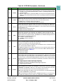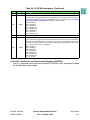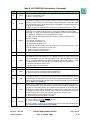
1
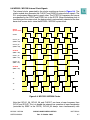
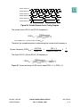
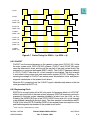
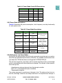
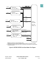
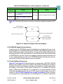
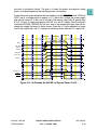
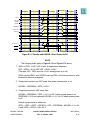
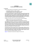
SECTION 8
CLOCKS AND POWER CONTROL
8.1 Overview
The main timing reference for the MPC555 / MPC556 can monitor any of the following:
• A crystal with a frequency of four MHz or 20 MHz
• An external frequency source with a frequency of 4 MHz
• An external frequency source at the system frequency
The system operating frequency is generated through a programmable phase-locked
loop, the system PLL (SPLL). The SPLL is programmable in integer multiples of the
input oscillator frequency to generate the internal (VCO/2) operating frequency. A predivider before the SPLL enables the user to divide the high frequency crystal oscillator.
The SPLL VCO is twice the system frequency. The internal operating SPLL frequency
should be at least 30 MHz. It can be divided by a power-of-two divider to generate the
system operating frequencies.
In addition to the system clock, the clocks submodule provides the following:
• TMBCLK to the time base (TB) and decrementer (DEC)
• PITRTCLK to the periodic interrupt timer (PIT) and real-time clock (RTC)
The oscillator, TB, DEC, RTC, and the PIT are powered from the keep alive power
supply (KAPWR) pin. This allows the counters to continue to count (increment/decrement) at the oscillator frequency even when the main power to the MCU is off. While
the power is off, the PIT may be used to signal to the power supply IC to enable power
to the system at specific intervals. This is the power-down wake-up feature. When the
chip is not in power-down low-power mode, the KAPWR is powered to the same voltage value as the voltage of the I/O buffers and logic.
The MPC555 / MPC556 clock module consists of the main crystal oscillator (OSCM),
the SPLL, the low-power divider, the clock generator, the system low-power control
block, and the limp mode control block. The clock module receives control bits from
the system clock control register (SCCR), change of lock interrupt register (COLIR),
the low-power and reset-control register (PLPRCR), and the PLL.
All of the MPC555 peripherals on the IMB bus derive its clock timing from the UIMB
module. The UIMB runs on the main system clock, but can divide the system frequency in half. See 12.3 Clock Module.
Figure 8-1 illustrates the functional block diagram of the clock unit.
MPC555 / MPC556
CLOCKS AND POWER CONTROL
USER’S MANUAL
Rev. 15 October 2000
MOTOROLA
8-1
VSSSYN
VDDSYN
XFC
MODCK[1:3]
EXTCLK
2:1
MUX
VCOOUT
2:1 MUX
SPLL
Lock
GCLK2
TBCLK
System Low-Power Control
Low
Power
Dividers
(1/2N)
Clock
Drivers
3:1 MUX
(/4 or /16)
GCLK1 / GCLK2
SYSTEM CLOCK
GCLK1C / GCLK2C
SYSTEM CLOCK
TO RCPU AND BBC
CLKOUT
Back_Up Clock
Oscillator Loss
3:1
Detector
MUX
Drivers
ENGCLK
TMBclk
Driver
TMBCLK
RTC / PIT Clock
and DRIVER
XTAL
Main Clock
Oscillator
PITRTCLK
/4 or /256
EXTAL
Figure 8-1 Clock Unit Block Diagram
MPC555 / MPC556
CLOCKS AND POWER CONTROL
USER’S MANUAL
Rev. 15 October 2000
MOTOROLA
8-2
8.2 System Clock Sources
The system clock can be provided by the main system oscillator (OSCM), an external
clock input, or the backup clock (BUCLK) on-chip ring oscillator, see Figure 8-2.
The OSCM uses either a 4-MHz or 20-MHz crystal to generate the PLL reference
clock. When the main system oscillator output is the timing reference to the system
PLL, skew elimination between the XTAL/EXTAL pins and CLKOUT is not guaranteed.
The external clock input receives a clock signal from an external source. The clock frequency must be either in the range of 3 MHz – 5 MHz or at the system frequency of at
least 15 MHz (1:1 mode). When the external clock input is the timing reference to the
system PLL skew elimination between the EXTCLK pin and the CLKOUT is less than
± 1 ns.
The backup clock on-chip ring oscillator enables the MCU to function with a less precise clock. When operating from the backup clock, the MCU is in limp mode. This enables the system to continue minimum functionality until the system is fixed. The
BUCLK frequency is approximately 7 MHz (see APPENDIX G ELECTRICAL CHARACTERISTICS for the complete frequency range).
For normal operation, at least one clock source (EXTCLK or OSCM) must be active.
A configuration with both clock sources active is possible as well. At this configuration
EXTCLK provides the OSCCLK and OSCM provides the PITRTCLK. The input of an
unused timing reference (EXTCLK or EXTAL) must be grounded.
XTAL
EXTAL
1 MΩ*
CL
CL
*Resistor is not currently required on the board but space should be available for its addition in the future.
Figure 8-2 Main System Oscillator (OSCM)
8.3 System PLL
The PLL allows the processor to operate at a high internal clock frequency using a low
frequency clock input, a feature which offers two benefits. Lower frequency clock input
reduces the overall electromagnetic interference generated by the system, and the
ability to oscillate at different frequencies reduces cost by eliminating the need to add
an additional oscillator to a system.
The PLL can perform the following functions:
• Frequency multiplication
MPC555 / MPC556
CLOCKS AND POWER CONTROL
USER’S MANUAL
Rev. 15 October 2000
MOTOROLA
8-3
• Skew elimination
• Frequency division
8.3.1 Frequency Multiplication
The PLL can multiply the input frequency by any integer between one and 4096. The
multiplication factor depends on the value of the MF[0:11] bits in the PLPRCR register.
While any integer value from one to 4096 can be programmed, the resulting VCO output frequency must be at least 15 MHz. The multiplication factor is set to a predetermined value during power-on reset as defined in Table 8-1.
8.3.2 Skew Elimination
The PLL is capable of eliminating the skew between the external clock entering the
chip (EXTCLK) and both the internal clock phases and the CLKOUT pin, making it useful for tight synchronous timings. Skew elimination is active only when the PLL is enabled and programmed with a multiplication factor of one or two (MF = 0 or 1). The
timing reference to the system PLL is the external clock input.
8.3.3 Pre-Divider
A pre-divider before the phase comparator enables additional system clock resolution
when the crystal oscillator frequency is 20 MHz. The division factor is determined by
the DIVF[0:4] bits in the PLPRCR.
8.3.4 PLL Block Diagram
As shown in Figure 8-3, the reference signal, OSCCLK, goes to the phase comparator. The phase comparator controls the direction (up or down) that the charge pump
drives the voltage across the external filter capacitor (XFC). The direction depends on
whether the feedback signal phase lags or leads the reference signal. The output of
the charge pump drives the VCO. The output frequency of the VCO is divided down
and fed back to the phase comparator for comparison with the reference signal,
OSCCLK. The MF values, zero to 4095, are mapped to multiplication factors of one to
4096. Note that when the PLL is operating in 1:1 mode (refer to Table 8-1), the multiplication factor is one (MF = 0). The PLL output frequency is twice the maximum system frequency. This double frequency is needed to generate GCLK1 and GCLK2
clocks. On power-up, with a four MHz or 20 MHz crystal and the default MF settings,
System Frequency (FREQSYS) will be 40 MHz and the system clock will be 20 MHz.
The equation for system frequency (FREQSYS) is shown below:
System Frequency (FREQSYS) =
OSCCLK
DIVF + 1
x (MF + 1) x 2 / 2
NOTE
When operating with the backup clock, the system clock (and CLKOUT) is one-half of the ring oscillator frequency. (i.e., the system
clock is a nominal seven MHz). The time base and PIT clocks will be
twice the system clock frequency.
MPC555 / MPC556
CLOCKS AND POWER CONTROL
USER’S MANUAL
Rev. 15 October 2000
MOTOROLA
8-4
The PLL maximum lock time is determined by the input clock to the phase detector.
The PLL locks within 500 input clock cycles.
NOTE
Upon initial system power up and after KAPWR is lost, an external
circuit must assert power on reset (PORESET). If limp mode will be
enabled during power-on reset, PORESET must be asserted for at
least 100,000 cycles of input PLL clock after a valid level has been
reached on the KAPWR supply. If limp mode will be disabled,
PORESET should be asserted for approximately 3 µs after a valid
level has been reached on the KAPWR supply.
Whenever power-on reset is asserted, the MF bits are set according to Table 8-1, and
the DFNH and DFNL bits in SCCR are set to the value of 0 (÷1 and 2), respectively.
XFC
OSCCLK
Division Factor
DIVF[0:4]
Feedback
Phase
Comparator
Up
Down
System
Frequency
(FREQSYS)
Charge
Pump
VCO
÷2
VDDSYN / VSSSYN
÷2
Clock
Delay
Multiplication Factor
MF[0:11]
Figure 8-3 System PLL Block Diagram
8.3.5 PLL Pins
The following pins are dedicated to the PLL operation:
• VDDSYN — Drain voltage. This is the VDD dedicated to the analog PLL circuits.
The voltage should be well-regulated and the pin should be provided with an extremely low impedance path to the VDD power rail. VDDSYN should be bypassed
to VSSSYN by a 0.1 µF capacitor located as close as possible to the chip package.
• VSSSYN — Source voltage. This is the VSS dedicated to the analog PLL circuits.
The pin should be provided with an extremely low impedance path to ground.
VSSSYN should be bypassed to VDDSYN by a 0.1 µF capacitor located as close
as possible to the chip package.
• XFC — External filter capacitor. XFC connects to the off-chip capacitor for the
PLL filter. One terminal of the capacitor is connected to XFC, and the other terminal is connected to VDDSYN.
The off-chip capacitor must have the following values:
MPC555 / MPC556
CLOCKS AND POWER CONTROL
USER’S MANUAL
Rev. 15 October 2000
MOTOROLA
8-5
0 < MF + 1 < 4
MF + 1 ≥ 4
(680 x (MF + 1) – 120) pF
1100 x (MF + 1) pF
Where MF = the value stored on MF[0:11]. This is one less than the desired frequency multiplication factor.
8.4 System Clock During PLL Loss of Lock
At reset, until the SPLL is locked, the SPLL output clock is disabled.
During normal operation (once the PLL has locked), either the oscillator or an external
clock source is generating the system clock. In this case, if loss of lock is detected and
the LOLRE (loss of lock reset enable) bit in the PLPRCR is cleared, the system clock
source continues to function as the PLL’s output clock. The USIU timers can operate
with the input clock to the PLL, so that these timers are not affected by the PLL loss of
lock. Software can use these timers to measure the loss-of-lock period. If the timer
reaches the user-preset software criterion, the MCU can switch to the backup clock by
setting the switch to backup clock (STBUC) bit in the SCCR, provided the limp mode
enable (LME) bit in the SCCR is set.
If loss of lock is detected during normal operation, assertion of HRESET (for example,
if LOLRE is set) disables the PLL output clock until the lock condition is met. During
hard reset, the STBUC bit is set as long as the PLL lock condition is not met and clears
when the PLL is locked. If STBUC and LME are both set, the system clock switches to
the backup clock, and the chip operates in limp mode until STBUC is cleared.
Every change in the lock status of the PLL can generate a maskable interrupt.
NOTE
When the VCO is the system clock source, chip operation is unpredictable while the PLL is unlocked. Note further that a switch to the
backup clock is possible only if the LME bit in the SCCR is set.
8.5 Low-Power Divider
The output of the PLL is sent to a low-power divider block. (In limp mode the BUCLK
is sent to a low-power divider block.) This block generates all other clocks in normal
operation, but has the ability to divide the output frequency of the VCO before it generates the general system clocks sent to the rest of the MPC555 / MPC556. The PLL
System Frequency (FREQSYS) is always divided by at least 2.
The purpose of the low-power divider block is to allow the user to reduce and restore
the operating frequencies of different sections of the MPC555 / MPC556 without losing
the PLL lock. Using the low-power divider block, the user can still obtain full chip operation, but at a lower frequency. This is called gear mode. The selection and speed
of gear mode can be changed at any time, with changes occurring immediately.
The low-power divider block is controlled in the system clock control register (SCCR).
The default state of the low-power divider is to divide all clocks by one. Thus, for a 40MHz system, the general system clocks are each 40 MHz.
MPC555 / MPC556
CLOCKS AND POWER CONTROL
USER’S MANUAL
Rev. 15 October 2000
MOTOROLA
8-6
8.6 MPC555 / MPC556 Internal Clock Signals
The internal clocks generated by the clocks module are shown in Figure 8-4. The
clocks module also generates the CLKOUT and ENGCLK external clock signals. The
PLL synchronizes these signals to each other. The PITRTCLK frequency and source
are specified by the RTDIV and RTSEL bits in the SCCR. When the backup clock is
functioning as the system clock, the backup clock is automatically selected as the time
base clock source and is twice the MPC555 / MPC556 system clock.
GCLK1
System Clock
GCLK2
GCLK1_50
(EBDF = 00)
GCLK2_50
(EBDF = 00)
CLKOUT
(EBDF = 00)
GCLK1_50
(EBDF = 01)
GCLK2_50
(EBDF = 01)
CLKOUT
(EBDF = 01)
T1
T2
T3
T4
Figure 8-4 MPC555 / MPC556 Clocks
Note that GCLK1_50, GCLK2_50, and CLKOUT can have a lower frequency than
GCLK1 and GCLK2. This is to enable the external bus operation at lower frequencies
(controlled by EBDF in the SCCR). GCLK2_50 always rises simultaneously with
MPC555 / MPC556
CLOCKS AND POWER CONTROL
USER’S MANUAL
Rev. 15 October 2000
MOTOROLA
8-7
GCLK2. When DFNH = 0, GCLK2_50 has a 50% duty cycle. With other values of
DFNH or DFNL, the duty cycle is less than 50%. Refer to Figure 8-7. GCLK1_50 rises
simultaneously with GCLK1. When the MPC555 / MPC556 is not in gear mode, the
falling edge of GCLK1_50 occurs in the middle of the high phase of GCLK2_50. EBDF
determines the division factor between GCLK1/GCLK2 and GCLK1_50/GCLK2_50.
During power-on reset, the MOCCK1, MODCK2, and MODCK3 pins determine the
clock source for the PLL and the clock drivers. These pins are latched on the positive
edge of PORESET. Their values must be stable as long as this line is asserted. The
configuration modes are shown in Table 8-1. MODCK1 specifies the input source to
the SPLL (OSCM or EXTCLK). MODCK1, MODCK2, and MODCK3 together determine the multiplication factor at reset and the functionality of limp mode.
If the configuration of PITRTCLK and TMBCLK and the SPLL multiplication factor is to
remain unchanged in power-down low-power mode, the MODCK signals should not
be sampled at wake-up from this mode. In this case the PORESET pin should remain
negated and HRESET should be asserted during the power supply wake-up stage.
When MODCK1 is cleared, the output of the main oscillator (OSCM) is selected as the
input to the SPLL. When MODCK1 is asserted, the external clock input (EXTCLK) is
selected as the input to the SPLL. In all cases, the system clock frequency (freqgclk2)
can be reduced by the DFNH[0:2] bits in the SCCR. Note that freqgclk2(max) occurs
when the DFNH bits are cleared.
The TBS bit in the SCCR selects the time base clock to be either the SPLL input clock
or GCLK2. When the backup clock is functioning as the system clock, the backup clock
is automatically selected as the time base clock source.
The PITRTCLK frequency and source are specified by the RTDIV and RTSEL bits in
the SCCR. When the backup clock is functioning as the system clock, the backup
clock is automatically selected as the time base clock source.
When the PORESET pin is negated (driven to a high value), the MODCK1, MODCK2,
and MODCK3 values are not affected. They remain the same as they were defined
during the most recent power-on reset.
Table 8-1 shows the clock configuration modes during power-on reset (PORESET asserted).
NOTE
The MODCK[1:3] are shared functions with IRQ[5:7]. If IRQ[5:7] are
used as interrupts, the interrupt source should be removed during
PORESET to insure the MODCK pins are in the correct state on the
rising edge of PORESET.
MPC555 / MPC556
CLOCKS AND POWER CONTROL
USER’S MANUAL
Rev. 15 October 2000
MOTOROLA
8-8
Table 8-1 Reset Clocks Source Configuration
Default Values @ PORESET
1
MODCK[1:3]
LME
000
SPLL Options
MF + 1
PITCLK
Division
TMBCLK
Division
0
513
4
4
Used for testing purposes.
001
0
1
256
16
Normal operation, PLL enabled.
Main timing reference is freq(OSCM) = 20 MHz.
Limp mode disabled.
010
1
5
256
4
Normal operation, PLL enabled.
Main timing reference is freq(OSCM) = 4 MHz.
Limp mode enabled.
011
1
1
256
16
Normal operation, PLL enabled.
Main timing reference is freq(OSCM) = 20 MHz.
Limp mode enabled.
100
101
0
1
256
16
Normal operation, PLL enabled. 1:1 Mode
freqclkout(max) = freq(EXTCLK)
Limp mode disabled.
110
0
5
256
4
Normal operation, PLL enabled.
Main timing reference is freq(EXTCLK) = 3-5 MHz.
Limp mode disabled.
111
1
1
256
16
Normal operation, PLL enabled. 1:1 Mode
freqclkout(max) = freq(EXTCLK)
Limp mode enabled.
NOTES:
1. For other implementations in the MPC500 family, MODCK2 could be inverted.
NOTE
The reset value of the PLL pre-divider is 1.
The values of the PITRTCLK clock division and TMBCLK clock division can be
changed by software. The RTDIV bit value in the SCCR register defines the division
of PITRTCLK. All possible combinations of the TMBCLK divisions are listed in Table
8-2.
Table 8-2 TMBCLK Divisions
SCCR[TBS]
MF + 1
TMBCLK
Division
1
—
16
0
1, 2
16
0
>2
4
8.6.1 General System Clocks
The general system clocks (GCLK1C, GCLK2C, GCLK1, GCLK2, GCLK1_50, and
GCLK2_50) are the basic clock supplied to all modules and sub-modules on the
MPC555 / MPC556. GCLK1C and GCLK2C are supplied to the RCPU and to the BBC.
GCLK1C and GCLK2C are stopped when the chip enters the doze-low power mode.
GCLK1 and GCLK2 are supplied to the SIU and the clock module. The external bus
clock GCLK2_50 is the same as CLKOUT. The general system clock defaults to VCO/
MPC555 / MPC556
CLOCKS AND POWER CONTROL
USER’S MANUAL
Rev. 15 October 2000
MOTOROLA
8-9
2 = 20 MHz (assuming a 20-MHz system frequency) with default power-on reset MF
values.
The general system clock frequency can be switched between different values. The
highest operational frequency can be achieved when the system clock frequency is
determined by DFNH (CSRC bit in the PLPRCR is cleared) and DFNH = 0 (division by
one). The general system clock can be operated at a low frequency (gear mode) or a
high frequency. The DFNL bits in SCCR define the low frequency. The DFNH bits in
SCCR define the high frequency.
The frequency of the general system clock can be changed dynamically with the system clock control register (SCCR), as shown in Figure 8-5.
VCO/2 (e.g., 40 MHz)
O
DFNH Divider
DFNH
Normal
O
O General System Clock
DFNL Divider
DFNL
O
Low Power
Figure 8-5 General System Clocks Select
The frequency of the general system clock can be changed “on the fly” by software.
The user may simply cause the general system clock to switch to its low frequency.
However, in some applications, there is a need for a high frequency during certain periods. Interrupt routines, for example, may require more performance than the low frequency operation provides, but must consume less power than in maximum frequency
operation. The MPC555 / MPC556 provides a method to automatically switch between
low and high frequency operation whenever one of the following conditions exists:
• There is a pending interrupt from the interrupt controller. This option is maskable
by the PRQEN bit in the SCCR.
• The (POW) bit in the MSR is clear in normal operation. This option is maskable
by the PRQEN bit in the SCCR.
When neither of these conditions exists and the CSRC bit in PLPRCR is set, the general system clock switches automatically back to the low frequency.
Abrupt changes in the divide ratio can cause linear changes in the operating currents
of the MPC555 / MPC556. Insure that the proper power supply filtering is available to
handle this change instantaneously.
When the general system clock is divided, its duty cycle is changed. One phase remains the same (e.g., 12.5 ns @ 40 MHZ) while the other become longer. Note that
CLKOUT does not have a 50% duty cycle when the general system clock is divided.
The CLKOUT waveform is the same as that of GCLK2_50.
MPC555 / MPC556
CLOCKS AND POWER CONTROL
USER’S MANUAL
Rev. 15 October 2000
MOTOROLA
8-10
GCLK1 Divide by 1
GCLK2 Divide by 1
GCLK1 Divide by 2
GCLK2 Divide by 2
GCLK1 Divide by 4
GCLK2 Divide by 4
Figure 8-6 Divided System Clocks Timing Diagram
The system clocks GCLK1 and GCLK2 frequency is:
FREQsysmax
FREQ sys = -------------------------------------------------------DFNH
DFNL + 1
(2
)or ( 2
)
where FREQsysmax = System Frequency (FREQSYS)/2
Therefore, the complete equation for determining the system clock frequency is:
System Frequency (FREQSYS) =
OSCCLK
DIVF + 1
(MF + 1)
x
(2DFNH or 2DFNL + 1)
x
2
2
The clocks GCLK1_50 and GCLK2_50 frequency is:
FREQsysmax
1
- × -------------------------FREQ50 = ------------------------------------------------------DFNH
DFNL + 1
EBDF
+1
(2
)or ( 2
)
Figure 8-7 shows the timing of USIU clocks when DFNH = 1 or DFNL = 0.
MPC555 / MPC556
CLOCKS AND POWER CONTROL
USER’S MANUAL
Rev. 15 October 2000
MOTOROLA
8-11
GCLK1
GCLK2
GCLK1_50
(EBDF = 00)
GCLK2_50
(EBDF = 00)
CLKOUT
(EBDF = 00)
GCLK1_50
(EBDF = 01)
GCLK2_50
(EBDF = 01)
CLKOUT
(EBDF = 01)
Figure 8-7 Clocks Timing For DFNH = 1 (or DFNL = 0)
8.6.2 CLKOUT
CLKOUT has the same frequency as the general system clock (GCLK2_50). Unlike
the main system clock GCLK1/GCLK2 however, CLKOUT (and GCLK2_50) represents the external bus clock, and thus will be one-half of the main system clock if the
external bus is running at half speed (EBDF = 0b01). The CLKOUT frequency defaults
to VCO/2. CLKOUT can drive full- or half-strength or be disabled. The drive strength
is controlled in the system clock and reset-control register (SCCR). Disabling or decreasing the strength of CLKOUT can reduce power consumption, noise, and electromagnetic interference on the printed circuit board.
When the PLL is acquiring lock, the CLKOUT signal is disabled and remains in the low
state (provided that BUCS = 0).
8.6.3 Engineering Clock
ENGCLK is an output clock with a 50% duty cycle. Its frequency defaults to VCO/1281,
which is one-sixtyfourth of the main system frequency. ENGCLK frequency can be programmed to the main system frequency divided by a factor from one to 64, as controlled by the ENGDIV[0:5] bits in the SCCR. ENGCLK can drive full- or half-strength
or be disabled (remaining in the high state). The drive strength is controlled by the EECLK[0:1] bits in the SCCR. Disabling ENGCLK can reduce power consumption, noise,
and electromagnetic interference on the printed circuit board.
1. Mask
sets prior to K62N default to VCO/4.
MPC555 / MPC556
CLOCKS AND POWER CONTROL
USER’S MANUAL
Rev. 15 October 2000
MOTOROLA
8-12
When the PLL is acquiring lock, the ENGCLK signal is disabled and remains in the low
state (provided that BUCS = 0).
NOTE
Skew elimination between CLKOUT and ENGCLK is not guaranteed.
8.7 Clock Source Switching
For limp mode support, clock source switching is supported. If for any reason the clock
source for the chip is not functioning, the user has the option to switch the system clock
to the backup clock ring oscillator, BUCLK.
This circuit consists of a loss-of-clock detector, which sets the LOCS status bit and
LOCSS sticky bit in the PLPRCR. If the LME bit in the SCCR is set, whenever LOCS
is asserted the clock logic switches the system clock automatically to BUCLK and asserts hard reset to the chip. Switching the system clock to BUCLK is also possible by
software setting the STBUC bit in SCCR. Switching from limp mode to normal system
operation is accomplished by clearing STBUC and LOCSS bits. This operation also
asserts hard reset to the chip.
At HRESET assertion, if the PLL output clock is not valid, the BUCLK will be selected
until software clears LOCSS bit in SCCR. At HRESET assertion, if the PLL output
clock is valid, the system will switch to oscillator/external clock. If during HRESET the
PLL loses lock or the clock frequency becomes slower than the required value, the
system will switch to the BUCLK. After HRESET negation, the PLL lock condition does
not effect the system clock source selection.
If the LME bit is clear, the switch to the backup clock is disabled and assertion of STBUC bit is ignored. If the chip is in limp mode, clearing the LME bit switches the system
to normal operation and asserts hard reset to the chip.
Figure 8-8 describes the clock switching control logic. Table 8-3 summarizes the status and control for each state.
MPC555 / MPC556
CLOCKS AND POWER CONTROL
USER’S MANUAL
Rev. 15 October 2000
MOTOROLA
8-13
LME = 1
poreset_b = 0
poreset_b = 0
1,BUCLK
poreset_b = 1
LME = 1
buclk_enable = 1
& hreset_b = 0
else
bu
cl
hr k _e
es n
et ab
_b le
= =0
1
buclk_enable=0
& hreset_b=0
4,osc
1
2,BUCLK
=
bu
c
hr lk_
es en
et ab
_b le
=
1
LME = 0
else
hreset_b = 1
hresert_b = 0
hreset_b = 1
bu
cl
k
as _ e
se na
rt ble
hr
es = 1
et
_b
3,BUCLK
6,BULCK
buclk-enable = 1
& hreset_b = 0
hreset_b = 0
LOCS
buclk_enable = 0
& hreset_b = 0
5, osc
else
Figure 8-8 Clock Source Flow Chart
NOTES
BUCLK_ENABLE = (STBUC | LOC) & LME lock indicates loss of lock
status bit (LOCS) for all cases and loss of clock sticky bit (LOCSS)
when state 3 is active. When BUCLK_ENABLE is changed, the chip
asserts HRESET to switch the system clock to BUCLK or PLL.
At PORESET negation, if the PLL is not locked, the loss-of-clock
sticky bit (LOCSS) is asserted, and the chip should operate with BUCLK.
MPC555 / MPC556
CLOCKS AND POWER CONTROL
USER’S MANUAL
Rev. 15 October 2000
MOTOROLA
8-14
The switching from state three to state four is accomplished by clearing the STBUC and LOCSS bits. If the switching is done when the
PLL is not locked, the system clock will not oscillate until lock condition is met.
Table 8-3 Status of Clock Source
STATE
PORESET
HRESET
LME
LOCS
(status)
LOCSS
(sticky)
STBUC
BUCS
Chip
Clock
Source
1
0
0
1
0
0
0
1
BUCLK
2
1
0
1
0/1
0
0
1
BUCLK
1
x2
0/1
0/1
1
BUCLK
0
0
Oscillator
3
1
1
1
4
1
0
0/1
0
x2
5
1
1
0/1
0
x2
0
0
Oscillator
6
1
0
1
0/1
1
0/1
1
BUCLK
NOTES:
1. At least one of the two bits, LOCSS or BUCS, must be asserted (one) in this state.
2. X = don’t care.
The default value of the LME bit is determined by MODCK[1:3] during assertion of
the PORESET line. The configuration modes are shown in Table 8-1.
8.8 Low-Power Modes
The LPM and other bits in the PLPRCR are encoded to provide one normal operating
mode and four low-power modes. In normal and doze modes the system can be in
high state with frequency defined by the DFNH bits, or in the low state with frequency
defined by the DFNL bits. The normal-high operating mode is the state out of reset.
This is also the state of the bits after the low-power mode exit signal arrives.
There are four low-power modes:
• Doze mode
• Sleep mode
• Deep-sleep mode
• Power-down mode
8.8.1 Entering a Low-Power Mode
Low-power modes are enabled by setting the POW bit in the MSR and clearing the
LPML (low-power mode lock) bit in the PLPRCR. Once enabled, a low-power mode is
entered by setting the LPM bits to the appropriate value. This can be done only in one
of the normal modes. The user cannot change the LPM or CSRC bits when the MCU
is in doze mode.
Table 8-6 summarizes the control bit descriptions for the different clock power modes.
MPC555 / MPC556
CLOCKS AND POWER CONTROL
USER’S MANUAL
Rev. 15 October 2000
MOTOROLA
8-15
Table 8-4 Power Mode Control Bit Descriptions
Power Mode
LPM[0:1]
CSRC
TEXPS
Normal-high
00
0
X
Normal-low (“gear”)
00
1
X
Doze-high
01
0
X
Doze-low
01
1
X
Sleep
10
X
X
Deep-sleep
11
X
1
Power-down
11
X
0
8.8.2 Power Mode Descriptions
Table 8-5 describes the power consumption, clock frequency, and chip functionality
for each power mode.
Table 8-5 Power Mode Descriptions
Operation Mode
SPLL
Clocks
Normal-high
Active
Full frequency ÷
2DFNH
Normal-low (“gear”)
Active
Full frequency ÷
2DFNL+1
Doze-high
Active
Full frequency ÷
2DFNH
Doze-low
Active
Full frequency ÷
2DFNL+1
Sleep
Active
Not active
Deep-sleep
Not active
Not active
Power-down
Not active
Not active
VDDSRAM
Not active
Not active
Functionality
Full functions not in use
are shut off
Enabled: RTC, PIT,
TB and DEC,
memory controller
Disabled: extended
core
(RCPU, BBC, FPU)
Enabled: RTC, PIT, TB
and DEC
SRAM’s data
retention
8.8.3 Exiting from Low-Power Modes
Exiting from low-power modes occurs through an asynchronous interrupt or a synchronous interrupt generated by the memory controller. Any enabled asynchronous interrupt clears the LPM bits but does not change the PLPRCR[CSRC] bit.
The exit from normal-low, doze-high, and low modes and sleep mode to normal-high
mode is accomplished with the asynchronous interrupt. The sources of the asynchronous interrupt are:
• Asynchronous wake-up interrupt from the interrupt controller
• RTC, PIT, or time base interrupts (if enabled)
• Decrementer exception
The system response to asynchronous interrupts is fast. The wake-up time from normal-low, doze-high, doze-low, and sleep mode due to an asynchronous interrupt or
MPC555 / MPC556
CLOCKS AND POWER CONTROL
USER’S MANUAL
Rev. 15 October 2000
MOTOROLA
8-16
decrementer exception is only three to four clock cycles of maximum system frequency. In 40-MHz systems, this wake-up requires 75 to 100 ns. The asynchronous wakeup interrupt from the interrupt controller is level sensitive one. It will therefore be negated only after the reset of interrupt cause in the interrupt controller.
The timers (RTC, PIT, time base, or decrementer) interrupts indication set status bits
in the PLPRCR (TMIST). The clock module considers this interrupt to be pending
asynchronous interrupt as long as the TMIST is set. The TMIST status bit should be
cleared before entering any low-power mode.
Table 8-7 summarizes wake-up operation for each of the low-power modes.
Table 8-6 Power Mode Wake-Up Operation
Operation Mode
Wake-up
Method
Return Time from Wake-up
Event to Normal-High
Normal-low (“gear”)
Software
or
Interrupt
Doze-high
Interrupt
Doze-low
Interrupt
Sleep
Interrupt
3-4 maximum system clocks
Deep-sleep
Interrupt
< 500 Oscillator Cycles
125 µsec – 4 MHz
25 µsec – 20 MHz
Power-down
Interrupt
< 500 oscillator cycles + power
supply wake-up
VDDSRAM
External
Power-on sequence
Asynchronous interrupts:
3-4 maximum system cycles
Synchronous interrupts:
3-4 actual system cycles
8.8.3.1 Exiting from Normal-Low Mode
In normal mode (as well as doze mode), if the PLPRCR[CSRC] bit is set, the system
toggles between low frequency (defined by PLPRCR[DFNL]) and high frequency (defined by PLPRCR[DFNH]. The system switches from normal-low mode to normal-high
mode if either of the following conditions is met:
• An interrupt is pending from the interrupt controller; or
• The MSR[POW] bit is cleared (power management is disabled).
When neither of these conditions are met, the PLPRCR[CSRC] bit is set, and the asynchronous interrupt status bits are reset, the system returns to normal-low mode.
8.8.3.2 Exiting from Doze Mode
The system changes from doze mode to normal-high mode whenever an interrupt is
pending from the interrupt controller.
8.8.3.3 Exiting from Deep-Sleep Mode
The system switches from deep-sleep mode to normal-high mode if any of the following conditions is met:
MPC555 / MPC556
CLOCKS AND POWER CONTROL
USER’S MANUAL
Rev. 15 October 2000
MOTOROLA
8-17
• An interrupt is pending from the interrupt controller
• An interrupt is requested by the RTC, PIT, or time base
• A decrementer exception
In deep-sleep mode the PLL is disabled. The wake-up time from this mode is up to 500
PLL input frequency clocks. In one-to-one mode the wake-up time may be up to 100
PLL input frequency clocks. For a PLL input frequency of 4 MHz, the wake-up time is
less than 125 µs.
8.8.3.4 Exiting from Power-Down Mode
Exit from power-down mode is accomplished through hard reset. External logic should
assert HRESET in response to the TEXPS bit being set and TEXP pin being asserted.
The TEXPS bit is set by an enabled RTC, PIT, time base, or decrementer interrupt.
The hard reset should be asserted for no longer than the time it takes for the power
supply to wake-up in addition to the PLL lock time. When the TEXPS bit is cleared (and
the TEXP signal is negated), assertion of hard reset sets the bit, causes the pin to be
asserted, and causes an exit from power-down low-power mode. Refer to 8.9.3 Keep
Alive Power for more information.
8.8.3.5 Low-Power Modes Flow
Figure 8-9 shows the flow among the different power modes.
MPC555 / MPC556
CLOCKS AND POWER CONTROL
USER’S MANUAL
Rev. 15 October 2000
MOTOROLA
8-18
(MSRPOW+Interrupt)+CSRC
Software *
Normal-Low
LPM = 00, CSRC = 1
Software *
((MSRPOW+Interrupt))*CSRC***
Doze-Low
LPM = 01, CSRC = 1
Interrupt
Wake-up: 3 - 4 SysFreq
Clocks
Software *
Asynchronous
Interrupts
Doze-High
LPM = 01, CSRC = 0/1
Wake-up: 3 - 4 SysFreqmax
Clocks
LPM = 00
CSRC = 0/1
Software *
Sleep Mode
LPM = 10, CSRC = 0
Software *
Deep-Sleep Mode
LPM = 11, CSRC = 0,
TEXPS = 1
Power-Down Mode
LPM = 11, CSRC = 0,
TEXPS = 0**
Software *
Normal
High Mode
Async. Wake-up or
RTC/PIT/TB/DEC Interrupt
Wake-up: 500 Input
Frequency Clocks
RTC/PIT/TB/DEC Interrupt followed
by External Hard Reset
or External Hard Reset
Software *
Hard Reset
* Software is active only in normal-high/low modes
** TEXPS receives the zero value by writing one. Writing of zero has no effect on TEXPS.
*** The switch from normal-high to normal-low is enable only if the conditions to asynchronous
interrupt are cleared
Figure 8-9 MPC555 / MPC556 Low-Power Modes Flow Diagram
MPC555 / MPC556
CLOCKS AND POWER CONTROL
USER’S MANUAL
Rev. 15 October 2000
MOTOROLA
8-19
8.9 Basic Power Structure
8.9.1 Clock Unit Power Supply
KAPWR and VSS power the following clock unit modules: oscillator, PITRTCLK and
TMBCLK generation logic, timebase, decrementer, RTC, PIT, system clock control
register (SCCR), low-power and reset-control register (PLPRCR), and reset status
register (RSR). All other circuits are powered by the normal supply pins, VDDI, VDDL,
VDDH and VSS. The power supply for each block is listed in Table 8-7.
Table 8-7 Clock Unit Power Supply
Circuit
CLKOUT
SPLL (digital),
System low-power control
Internal logic
Clock drivers
Power Supply
VDDL/VDDI
SPLL (analog)
VDDSYN
Main oscillator
Reset machine
Limp mode mechanism
Register control
SCCR, PLLRCR and RSR
RTC, PIT, TB, and DEC
KAPWR
SRAM,
VDDSRAM detector,
VSRMCR
VDDSRAM
The following are the relations between different power supplies:
• VDDL = VDDI = VDDSYN = VDDF = 3.3 V ±10%
• KAPWR ≥ VDDL – 0.2 V (during normal operation)
• VDDSRAM ≥ VDDL – 0.3 V (during normal operation)
• VDDSRAM ≥ 1.4 V (during standby operation)
• VPP ≥ VDDL – 0.3 V, but VPP – VDDL < 4.0 volts
8.9.2 Chip Power Structure
The MPC555 / MPC556 provides a wide range of possibilities for power supply connections. Figure 8-10 illustrates the different power supply sources for each of the basic units on the chip.
8.9.2.1 VDDL
The I/O buffers and logic are fed by a 3.3-V power supply.
8.9.2.2 VDDI
VDDI powers the internal logic of the MPC555 / MPC556, nominally 3.3 V.
MPC555 / MPC556
CLOCKS AND POWER CONTROL
USER’S MANUAL
Rev. 15 October 2000
MOTOROLA
8-20
8.9.2.3 VDDSYN, VSSSYN
The charge pump and the VCO of the SPLL are fed by a separate 3.3-V power supply
(VDDSYN) in order to improve noise immunity and achieve a high stability in its output
frequency. VSSSYN provides an isolated ground reference for the PLL.
8.9.2.4 KAPWR
The oscillator, time base counter, decrementer, periodic interrupt timer and the realtime clock are fed by the KAPWR rail. This allows the external power supply unit to
disconnect all other sub-units of the MCU in low-power deep-sleep mode. The TEXP
pin (fed by the same rail) can be used by the external power supply unit to switch between sources. The IRQ[6:7]/MODCK[2:3], IRQ[5]/MODCK1, XTAL, EXTAL, EXTCLK, PORESET, HRESET, SRESET, and RSTCONF/TEXP input pins are powered
by KAPWR. Circuits, including pull-up resisters, driving these inputs should be powered by KAPWR.
8.9.2.5 VDDA, VSSA
VDDA supplies power to the analog subsystems of the QADC_A and QADC_B modules; it is nominally 5.0 V. VDDA is the ground reference for the analog subsystems.
8.9.2.6 VPP
VPP supplies the programming and erase voltage for the CMF flash modules. It is
nominally 5.0 V for program or erase operations and can be lowered to a nominal 3.3
V for read operations.
8.9.2.7 VDDF, VSSF
VDDF provides internal power to the CMF flash module; it should be a nominal 3.3 V.
VSSF provides an isolated ground for the CMF flash module.
8.9.2.8 VDDH
VDDH provides power for the 5-V I/O operations. It is a nominal 5.0 V.
8.9.2.9 VDDSRAM
VDDSRAM supplies power to the 26-Kbyte SRAM module and the DPTRAM. It can
be used to keep the contents on the SRAM stable while the rest of the MPC555 /
MPC556 is powered down for standby operation.
8.9.2.10 VSS
VSS provides the ground reference for the MPC555 / MPC556.
MPC555 / MPC556
CLOCKS AND POWER CONTROL
USER’S MANUAL
Rev. 15 October 2000
MOTOROLA
8-21
VPP
VDDF
I/O
VDDH
SRAM
FLASH
Oscillator,
PIT, RTC, TB,
and DEC
Internal Logic
Clock Control
PLL
VDDI
VDDSRAM
TEXP
KAPWR
VDDI
VDDL
VDDSYN
Figure 8-10 Basic Power Supply Configuration
8.9.3 Keep Alive Power
8.9.3.1 Keep Alive Power Configuration
Figure 8-11 illustrates an example of a switching scheme for an optimized low-power
system. SW1 and SW2 can be unified in only one switch if VDDSYN and VDDI/VDDL
are supplied by the same source.
MPC555 / MPC556
CLOCKS AND POWER CONTROL
USER’S MANUAL
Rev. 15 October 2000
MOTOROLA
8-22
SW1
O
VDDSYN
Main Power
Supply
O
O
VDD
3.3 V
SW2
O
MPC555
TEXP
Switch
Logic
VDDSRAM
VDDSRAM
Power Supply
3.3 V
KAPWR
3 V - 3.3 V
Backup
Power
Supply
Figure 8-11 External Power Supply Scheme
The MPC555 / MPC556 asserts the TEXP signal, if enabled, when the RTC or TB time
value matches the value programmed in the associated alarm register or when the PIT
or DEC value reaches zero. The TEXP signal is negated when the TEXPS status bit
is written to one.
The KAPWR power supply feeds the main crystal oscillator (OSCM). The condition for
the main crystal oscillator stability is that the power supply value changes slowly. The
maximum slope must be less than 5 mV per oscillation cycle (τ > 200-300/freqoscm).
8.9.3.2 Keep Alive Power Registers Lock Mechanism
The USIU timer, clocks, reset, power, decrementer, and time base registers are powered by the KAPWR supply. When the main power supply is disconnected after powerdown mode is entered, the value stored in any of these registers is preserved. If power-down mode is not entered before power disconnect, there is a chance of data loss
in these registers. To minimize the possibility of data loss, the MPC555 / MPC556 includes a key mechanism that ensures data retention as long as a register is locked.
While a register is locked, writes to this register are ignored.
Each of the registers in the KAPWR region have a key that can be in one of two states:
open or locked. At power-on reset the following keys are locked: RTC, RTSEC, RT-
MPC555 / MPC556
CLOCKS AND POWER CONTROL
USER’S MANUAL
Rev. 15 October 2000
MOTOROLA
8-23
CAL, and RTCSC. All other registers are unlocked. Each key has an address associated with it in the internal memory map.
A write of 0x55CCAA33 to the associated key register changes the key to the open
state. A write of any other data to this location changes the key to the locked state.
NOTE
A read of a key register may be interpreted as a write of a lock value
and may lock the associated KAPWR register.
The key registers are write-only. A read of the key register has undefined side effects
and may be interpreted as a write that locks the associated register.
Table 8-8 lists the registers powered by KAPWR and the associated key registers.
Table 8-8 KAPWR Registers and Key Registers
KAPWR Register
Address or
SPR Number
Associated Key Register
Register
Address
Register
0x2F C200
Time Base Status and Control (TBSCR)
See Table 6-16 for bit descriptions.
0x2F C204
Time Base Reference 0 (TBREF0)
See 6.13.4.3 Time Base Reference Reg- 0x2F C304
isters for bit descriptions.
Time Base Reference 0 Key (TBREF0K)
0x2F C208
Time Base Reference 1 (TBREF1)
See 6.13.4.3 Time Base Reference Reg- 0x2F C308
isters for bit descriptions.
Time Base Reference 1 Key (TBREF1K)
0x2F C220
Real Time Clock Status and Control
(RTCSC)
See Table 6-17 for bit descriptions.
0x2F C320
Real Time Clock Status and Control Key
(RTCSCK)
0x2F C224
Real Time Clock (RTC)
See 6.13.4.6 Real-Time Clock Register
(RTC) for bit descriptions.
0x2F C324
Real Time Clock Key (RTCK)
0x2F C228
Real Time Alarm Seconds (RTSEC)
Reserved
0x2F C328
Real Time Alarm Seconds Key (RTSECK)
0x2F C22C
Real Time Alarm (RTCAL)
See 6.13.4.7 Real-Time Clock Alarm
Register (RTCAL) for bit descriptions.
0x2F C32C
Real Time Alarm Key (RTCALK)
0x2F C240
PIT Status and Control (PISCR)
See Table 6-18 for bit descriptions.
0x2F C340
PIT Status and Control Key (PISCRK)
0x2F C244
PIT Count (PITC)
See Table 6-19 for bit descriptions.
0x2F C344
PIT Count Key (PITCK)
0x2F C280
System Clock Control Register (SCCR)
See Table 8-9 for bit descriptions.
0x2F C380
System Clock Control Key (SCCRK)
0x2F C284
PLL Low-Power and Reset-Control
Register (PLPRCR)
See Table 8-10 for bit descriptions.
0x2F C384
PLL Low-Power and Reset-Control Register Key (PLPRCRK)
0x2F C288
Reset Status Register (RSR)
See Table 7-3 for bit descriptions.
0x2F C388
Reset Status Register Key (RSRK)
0x2F C300
Time Base Status and Control Key
(TBSCRK)
MPC555 / MPC556
CLOCKS AND POWER CONTROL
USER’S MANUAL
Rev. 15 October 2000
MOTOROLA
8-24
Table 8-8 KAPWR Registers and Key Registers (Continued)
KAPWR Register
Associated Key Register
Address or
SPR Number
Register
SPR 22
Decrementer
See 3.9.5 Decrementer Register (DEC)
for bit descriptions.
SPR 268, 269,
284, 285,
Time Base
See Table 3-11 and Table 3-14 for bit descriptions.
Address
0x2F C30C
Register
Time Base and Decrementer Key (TBK)
Figure 8-12 illustrates the process of locking or unlocking a register powered by KAPWR.
Power On Reset
(Valid for other registers)
Open
Write to the Key 0x55CCAA33
Write to the key other value
Locked
Power On Reset
(Valid for RTC, RTSEC,
RTCAL and RTCSC)
Figure 8-12 Keep Alive Register Key State Diagram
8.10 VDDSRAM Supply Failure Detection
A special circuit for VDDSRAM supply failure detection is provided. In the case of supply failure detection, the dedicated sticky bits LVSRS in the VSRMCR register are asserted. Software can read or clear these bits. The user should enable the detector and
then clear these bits. If the user reads any of the LVSR bits as one, then a power failure
of VDDSRAM has occurred. The circuit is capable of detecting supply failure below 2.6
V. Also, enable/disable control bit for the VDDSRAM detector may be used to disconnect the circuit and save the detector power consumption.
8.11 Power Up/Down Sequencing
Figure 8-13 and Figure 8-14 detail the power-up sequencing for MPC555 / MPC556
during normal operation. Note that for each of the conditions detailing the voltage relationships the absolute bounds of the minimum and maximum voltage supply cannot
be violated, i.e. the value of VDDL cannot fall below 3.0 V or exceed 3.6 V and the
value of VDDH cannot fall below 4.5 V or exceed 5.5 V for normal operation. Further
information detailing the functionality of the VPP signal for flash program and erase is
outlined in 19.9.2 FLASH Program/Erase Voltage Conditioning. Power consumption during power up sequencing can not be specified prior to evaluation and charac-
MPC555 / MPC556
CLOCKS AND POWER CONTROL
USER’S MANUAL
Rev. 15 October 2000
MOTOROLA
8-25
terization of production silicon. The goal is to keep the power consumption during
power up sequencing below the operating power consumption.
During the power down sequence the user needs to assert PORESET while VDDI and
VDDL are at a voltage equal or greater to 3 V. Below this voltage the power supply
chip can be turned off. If the turn off voltage of the power supply chip is greater than
0.74 V for the 3-V supply and greater than 0.8 V for the 5-V supply, then the circuitry
inside the MPC555 / MPC556 will act as a load to the respective supply and will discharge the supply line down to these values. Since the 3-V logic represents a larger
load to the supply chip, the 3-V supply line will decay faster than the 5-V supply line.
Power On
Power Off
Operating
See Note 1.
See Note 2.
VDDH
VDD, NVVL,
QVDDL
KAPRR
VDDSRAM
VDDA, VRH
VDDSYN
VFLASH (5 V)
PORESET
HRESET
Figure 8-13 No Standby, No KAPWR, All System Power On/Off
MPC555 / MPC556
CLOCKS AND POWER CONTROL
USER’S MANUAL
Rev. 15 October 2000
MOTOROLA
8-26
No Battery
Connect Battery
Power On
Operating
Power Off
No Battery
VDDH
VDD, NVVL,
QVDDL
KAPRR
VDDSRAM
VDDA, VRH
VDDSYN
VFLASH (5 V)
PORESET
HRESET
Figure 8-14 Standby and KAPWR, Other Power-On/Off
NOTE
The following notes apply to Figure 8-13 and Figure 8-14 above:
1. VDDH ≥ VDDL - 0.35 V (0.5 V max. at temperature extremes)
VPP ≤ VDDH + 0.5 V AND VPP ≥ VDDL - 0.35 V
(The delta VPP - VDDL must be ≤ 3.6 V during power on or off)
VDDA can lag VDDH, and VDDSYN can lag VDDL, but both must be at a valid
level before resets are negated.
2. If keep alive functions are NOT used, then when system power is on:
KAPWR = VDDSRAM = VDDL ± 0.35 V
3. If keep alive functions ARE used, then
KAPWR = VDDSRAM = VDDL = 3.3 V ± 0.35 V when system power is on
VDDSRAM ≥ 1.8 V and optionally KAPWR = 3.3 V ± 0.3 V when system power
is off
Normal system power is defined as
VDDL = VDDI = VDDF = VDDSYN = VPP = VDDSRAM = KAPWR = 3.3 ± 0.3
V and VDDA = VDDH = 5.0 ± 0.5 V
MPC555 / MPC556
CLOCKS AND POWER CONTROL
USER’S MANUAL
Rev. 15 October 2000
MOTOROLA
8-27
Flash programming requirements are the same as normal system power, except VPP = 5.0 ± 0.25 V
4. Do not hold the 3-V supplies at ground while VDDH/VDDA is ramping to 5 V.
5. If 5 V is applied before the 3-V supply, all 5-V outputs will be in indeterminate
states until the 3-V supply reaches a level that allows reset to be distributed
throughout the device
8.12 Clocks Unit Programming Model
8.12.1 System Clock Control Register (SCCR)
The SPLL has a 32-bit control register, SCCR, which is powered by keep-alive power.
SCCR — System Clock Control Register
MSB
0
1
2
DBCT
3
4
5
6
DCSLR
MFPDL
LPML
TBS
ID21
0
0
0
0
12
0
0
1
EQ23
ID21
U
0
0
U
U
U
0
1
U
19
20
21
22
23
24
25
26
COM
7
0x2F C280
8
9
10
11
RERTDIV2 STBUC SERVED PRQEN RTSEL
12
13
BUCS
14
15
EBDF
LME
ID[13:14]1
EQ34
ID[13:14]1
U
POWER-ON RESET:
1
0
HARD RESET:
U
0
16
17
18
ENGDIV5
EECLK
—
27
DFNL
U
28
29
—
30
LSB
31
DFNH
POWER-ON RESET:
0
0
1
1
1
1
1
1
U
U
U
U
U
U
0
0
0
0
0
0
0
0
0
0
0
0
0
0
0
HARD RESET:
U
U
NOTES:
1. The hard reset value is a reset configuration word value, extracted from the indicated internal data bus lines.
Refer to 7.5.2 Hard Reset Configuration Word.
U = Unaffected by reset
2. RTDIV will be 0 if MODCK[1:3] = 0b000
3. EQ2 = MODCK1
4. EQ3 = (MODCK1 & MODCK2 & MODCK3) | (MODCK1 & MODCK2 & MODCK3) | (MODCK1 & MODCK2 &
MODCK3). See Table 8-1.
5. On mask sets prior to K62N, ENGDIV defaults to 0b000001.
MPC555 / MPC556
CLOCKS AND POWER CONTROL
USER’S MANUAL
Rev. 15 October 2000
MOTOROLA
8-28
Table 8-9 SCCR Bit Descriptions
Bit(s)
0
1:2
3
4
5
6
Name
Description
DBCT
Disable backup clock for timers. The DBCT bit controls the timers clock source while the chip
is in limp mode. If DBCT is set, the timers clock (tbclk, rtclk) source will not be the backup
clock, even if the system clock source is the backup clock ring oscillator. The real-time clock
source will be EXTAL or EXTCLK according to RTSEL bit (see description in bit 11 below),
and the time base clocks source will be determined according to TBS bit and MODCK1.
0 = If the chip is in limp mode, the timer clock source is the backup (limp) clock
1 = The timer clock source is either the external clock or the crystal (depending on the current
clock mode selected)
COM
Clock output mode. These bits control the output buffer strength of the CLKOUT and external
bus pins. These bits can be dynamically changed without generating spikes on the CLKOUT
and external bus pins. If CKLOUT is not connected to external circuits, set both bits (disabling CLKOUT) to minimize noise and power dissipation. COM1 is determined by the hard
reset configuration word.
00 = Clock output enabled full-strength output buffer, bus pins full drive
01 = Clock output enabled half-strength output buffer, bus pins reduced drive
10 = Clock output disabled, bus pins full drive
11 = Clock output disabled, bus pins reduced drive
DCSLR
Disable clock switching at loss of lock during reset. When DCSLR is clear and limp mode is
enabled, the chip will switch automaticaly to the backup clock if the PLL losses lock during
HRESET. When DCSLR is asserted, a PLL loss-of-lock event does not cause clock switching. If HRESET is asserted and DCSLR is set, the chip will not negate HRESET until the PLL
aquires lock.
0 = Enable clock switching if the PLL loses lock during reset
1 = Disable clock switching if the PLL loses lock during reset
MFPDL
MF and pre-divider lock. Setting this control bit disables writes to the MF and DIVF bits. This
helps prevent runaway software from changing the VCO frequency and causing the SPLL to
lose lock. In addition, to protect against hardware interference, a hardware reset will be asserted if these fields are changed while LPML is asserted. This bit is writable once after power-on reset.
0 = MF and DIVF fields are writable
1 = MF and DIVF fields are locked
LPML
LPM lock. Setting this control bit disables writes to the LPM and CSRC control bits. In addition, for added protection, a hardware reset is asserted if any mode is entered other than normal-high mode. This protects against runaway software causing the MCU to enter low-power
modes. (The MSR[POW] bit provides additional protection). LPML is writable once after
power-on reset.
0 = LPM and CSRC bits are writable
1 = LPM and CSRC bits are locked and hard reset will occur if the MCU is not in normal-high
mode
TBS
Time base source. Note that when the chip is operating in limp mode (BUCS = 1), TBS is
ignored, and the backup clock is the time base clock source.
0 = Source is OSCCLK divided by either four or 16
1 = Source is system clock divided by 16
RTDIV
RTC (and PIT) clock divider. At power-on reset this bit is cleared if MODCK[1:3] are all low;
otherwise the bit is set.
0 = RTC and PIT clock divided by four
1 = RTC and PIT clock divided by 256
8
STBUC
Switch to backup clock control. When software sets this bit, the system clock is switched to
the on-chip backup clock ring oscillator, and the chip undergoes a hard reset. The STBUC
bit is ignored if LME is cleared.
0 = Do not switch to the backup clock ring oscillator
1 = Switch to backup clock ring oscillator
9
—
7
Reserved
MPC555 / MPC556
CLOCKS AND POWER CONTROL
USER’S MANUAL
Rev. 15 October 2000
MOTOROLA
8-29
Table 8-9 SCCR Bit Descriptions (Continued)
Bit(s)
10
11
12
13:14
Name
Description
PRQEN
Power management request enable
0 = Remains in the lower frequency (defined by DFNL) even if the power management bit in
the MSR is reset (normal operational mode) or if there is a pending interrupt from the
interrupt controller
1 = Switches to high frequency (defined by DFNH) when the power management bit in the
MSR is reset (normal operational mode) or there is a pending interrupt from the interrupt
controller
RTSEL
RTC circuit input source select. At power-on reset RTSEL receives the value of the
MODCK1 bit. Note that if the chip is operating in limp mode (BUCS = 0), the RTSEL bit is
ignored, and the backup clock is the clock source for the RT and PIT clocks
0 = OSCM clock is selected as input to RTC and PIT
1 = EXTCLK clock is selected as the RTC and PIT clock source
BUCS
Backup clock status. This status bit indicates the current system clock source. When loss of
clock is detected and the LME bit is set, the clock source is the backup clock and this bit is
set. When the user sets the STBUC bit and LME bit is set, the system switches to the backup
clock and BUCS is set.
0 = System clock is not the backup clock
1 = System clock is the backup clock
EBDF
External bus division factor. These bits define the frequency division factor between (GCLK1
and GCLK2) and (GCLK1_50 and GCLK2_50). CLKOUT is similar to GCLK2_50. The
GCLK2_50 and GCKL1_50 are used by the external bus interface and memory controller in
order to interface to the external system. The EBDF bits are initialized during hard reset using the hard reset configuration mechanism.
00 = CLKOUT is GCKL2 divided by 1
01 = CLKOUT is GCKL2 divided by 2
1x = Reserved
Limp mode enable. When LME is set, the loss-of-clock monitor is enabled and any detection
of loss of clock will switch the system clock automatically to backup clock. It is also possible
to switch to the backup clock by setting the STBUC bit.
15
LME
If LME is cleared, the option of using limp mode is disabled. The loss of clock detector is not
active, and any write to STBUC is ignored.
The LME bit is writable once, by software, after power-on reset, when the system clock is not
backup clock (BUCS = 0). During power-on reset, the value of LME is determined by the
MODCK[1:3] bits. (Refer to Table 8-1.)
0 = Limp mode disabled
1 = Limp mode enabled
16:17
EECLK
Enable engineering clock. This field controls the output buffer strength of the ENGCLK pin.
When both bits are set the ENGCLK pin is held in the high state. These bits can be dynamically changed without generating spikes on the ENGCLK pin. If ENGCLK is not connected
to external circuits, set both bits (disabling ENGCLK) to minimize noise and power dissipation. For measurement purposes the backup clock (BUCLK) can be driven externally on the
ENGCLK pin.
00 = Engineering clock enabled, full-strength output buffer
01 = Engineering clock enabled, half-strength output buffer
10 = BUCLK is the output on the ENGCLK full-strength output buffer
11 = Engineering clock disabled
Engineering clock division factor. These bits define the frequency division factor between
VCO/2 and ENGCLK. The divider ratio is ENGDIV+1. Division factor can be from 1 (ENGDIV
= 0b000000) to 64 (ENGDIV = 0b111111). These bits can be read and written at any time.
They are not affected by hard reset but are cleared during power-on reset.
18:23
ENGDIV
NOTE: If the engineering clock division factor is not a power of two, synchronization between
the system and ENGCLK is not guaranteed.
NOTE: The default (Power On Reset) value of ENGDIV will be 0b111111 on all mask sets
after K62N. The default for previous mask sets (J76N, K02A, and K83H) is 0b000001.
MPC555 / MPC556
CLOCKS AND POWER CONTROL
USER’S MANUAL
Rev. 15 October 2000
MOTOROLA
8-30
Table 8-9 SCCR Bit Descriptions (Continued)
Bit(s)
Name
24
—
25:27
DFNL
28
—
29:31
DFNH
Description
Reserved
Division factor low frequency. The user can load these bits with the desired divide value and
the CSRC bit to change the frequency. Changing the value of these bits does not result in a
loss of lock condition. These bits are cleared by power-on or hard reset. Refer to 8.6.1 General System Clocks and Figure 8-5 for details on using these bits.
000 = Divide by 2
001 = Divide by 4
010 = Divide by 8
011 = Divide by 16
100 = Divide by 32
101 = Divide by 64
110 = Reserved
111 = Divide by 256
Reserved
Division factor high frequency. These bits determine the general system clock frequency during normal mode. Changing the value of these bits does not result in a loss of lock condition.
These bits are cleared by power-on or hard reset. The user can load these bits at any time
to change the general system clock rate. Note that the GCLKs generated by this division factor are not 50% duty cycle (i.e. CLKOUT).
000 = Divide by 1
001 = Divide by 2
010 = Divide by 4
011 = Divide by 8
100 = Divide by 16
101 = Divide by 32
110 = Divide by 64
111 = Reserved
8.12.2 PLL, Low-Power, and Reset-Control Register (PLPRCR)
The PLL, low-power, and reset-control register (PLPRCR) is a 32-bit register powered
by the keep alive power supply.
MPC555 / MPC556
CLOCKS AND POWER CONTROL
USER’S MANUAL
Rev. 15 October 2000
MOTOROLA
8-31
PLPRCR — PLL, Low-Power, and Reset-Control Register
MSB
0
1
2
3
4
5
6
7
8
9
0x2F C284
10
11
12
13
RESERVE LOCS
D
MF
14
15
LOCSS
SPLS
POWER-ON RESET:
0 OR 4
0
0
0
0
U
U
U
U
HARD RESET:
U
U
16
17
SPLS
S
U
U
U
18
19
20
U
21
U
U
22
RERETEXP
SERVE TMIST SERVE CSRC
S
D
D
23
LPM
U
U
U
U
24
25
26
CSR
LOLRE
RESERVE
D
0
27
28
29
30
LSB
31
DIVF
POWER-ON RESET:
0
1
0
0
0
0
0
0
0
0
0
U
0
0
0
U
U
0
0
0
0
0
U
U
U
U
U
HARD RESET:
U
1
U
U = Unaffected by reset
Table 8-10 PLPRCR Bit Descriptions
Bit(s)
Name
Description
Multiplication factor bits. The output of the VCO is divided to generate the feedback signal to
the phase comparator. The MF bits control the value of the divider in the SPLL feedback
loop. The phase comparator determines the phase shift between the feedback signal and
the reference clock. This difference results in either an increase or decrease in the VCO output frequency.
0:11
MF
The MF bits can be read and written at any time. However, this field can be write-protected
by setting the MF and pre-divider lock (MFPDL) bit in the SCCR. Changing the MF bits causes the SPLL to lose lock. Also, the MF field should not be modified when entering or exiting
from low power mode (LPM change), or when back-up clock is active.
The normal reset value for the DFNH bits is zero (divide by one). When the PLL is operating
in one-to-one mode, the multiplication factor is set to x1 (MF = 0).
12
13
14
—
Reserved
LOCS
Loss of clock status. When the oscillator or external clock source is not at the minimum frequency, the loss-of-clock circuit asserts the LOCS bit. This bit is cleared when the oscillator
or external clock source is functioning normally. This bit is reset only on power-on reset.
Writes to this bit have no effect.
0 = No loss of oscillator is currently detected
1 = Loss of oscillator is currently detected
LOCSS
Loss of clock sticky. If, after negation of PORESET, the loss-of-clock circuit detects that the
oscillator or external clock source is not at a minimum frequency, the LOCSS bit is set. LOCSS remains set until software clears it by writing a one to it. A write of zero has no effect on
this bit. The reset value is determined during hard reset. The STBUC bit will be set provided
the PLL lock condition is not met when HRESET is asserted, and cleared if the PLL is locked
when HRESET is asserted.
0 = No loss of oscillator has been detected
1 = Loss of oscillator has been detected
MPC555 / MPC556
CLOCKS AND POWER CONTROL
USER’S MANUAL
Rev. 15 October 2000
MOTOROLA
8-32
Table 8-10 PLPRCR Bit Descriptions (Continued)
Bit(s)
Name
15
SPLS
16
SPLSS
Description
System PLL lock status bit
0 = SPLL is currently not locked
1 = SPLL is currently locked
SPLL lock status sticky bit. An out-of-lock sets the SPLSS bit. The bit remains set until software clears it by writing a one to it. A write of zero has no effect on this bit. The bit is cleared
at power-on reset. This bit is not affected due to a software initiated loss-of-lock (MF change
and entering deep-sleep or power-down mode). The SPLSS bit is not affected by hard reset.
0 = SPLL has remained in lock
1 = SPLL has gone out of lock at least once (not due to software-initiated loss of lock)
Timer expired status bit. This bit controls whether the chip negates the TEXP pin in deepsleep mode, thus enabling external circuitry to switch off the VDD (power-down mode).
When LPM = 11, CSRC = 0, and TEXPS is high, the TEXP pin remains asserted. When LPM
= 11, CSRC = 0, and TEXPS is low, the TEXPS pin is negated.
17
TEXPS
To enable automatic wake-up TEXPS is asserted when one of the following occurs:
• The PIT is expired
• The real-time clock alarm is set
• The time base clock alarm is set
• The decrementer exception occurs
The bit remains set until software clears it by writing a one to it. A write of zero has no effect
on this bit. TEXPS is set by power-on or hard reset.
0 = TEXP is negated in deep-sleep mode
1 = TEXP pin remains asserted always
18
—
19
TMIST
20
—
21
CSRC
22:23
24
25
Reserved
Timers interrupt status.TMIST is set when an interrupt from the RTC, PIT, TB or DEC occurs.
The TMIST bit is cleared by writing a one to it. Writing a zero has no effect on this bit. The
system clock frequency remains at its high frequency value (defined by DFNH) if the TMIST
bit is set, even if the CSRC bit in the PLPRCR is set (DFNL enabled) and conditions to switch
to normal-low mode do not exist. This bit is cleared during power-on or hard reset.
0 = No timer expired event was detected
1 = A timer expire event was detected
Reserved
Clock source. This bit is cleared at hard reset.
0 = General system clock is determined by the DFNH value
1 = General system clock is determined by the DFNL value
LPM
Low-power mode select. These bits are encoded to provide one normal operating mode and
four low-power modes. In normal and doze modes, the system can be in high state (frequency determined by the DFNH bits) or low state (frequency defined by the DFNL bits). The LPM
field can be write-protected by setting the LPM and CSRC lock (LPML) bit in the PLPRCR
Refer to Table 8-4 and Table 8-5.
CSR
Checkstop reset enable. If this bit is set, then an automatic reset is generated when the
RCPU signals that it has entered checkstop mode, unless debug mode was enabled at reset.
If the bit is clear and debug mode is not enabled, then the USIU will not do anything upon
receiving the checkstop signal from the RCPU. If debug mode is enabled, then the part enters debug mode upon entering checkstop mode. In this case, the RCPU will not assert the
checkstop signal to the reset circuitry. This bit is writable once after soft reset.
0 = No reset will occur when checkstop is asserted
1 = Reset will occur when checkstop is asserted
LOLRE
Loss of lock reset enable
0 = Loss of lock does not cause HRESET assertion
1 = Loss of lock causes HRESET assertion
Note: if limp mode is enabled, use the COLIR feature instead of setting the LOLRE bit. See
8.12.3 Change of Lock Interrupt Register (COLIR).
MPC555 / MPC556
CLOCKS AND POWER CONTROL
USER’S MANUAL
Rev. 15 October 2000
MOTOROLA
8-33
Table 8-10 PLPRCR Bit Descriptions (Continued)
Bit(s)
Name
26
—
27:31
DIVF
Description
Reserved
The DIVF bits control the value of the pre-divider in the SPLL circuit. The DIVF bits can be
read and written at any time. However, the DIVF field can be write-protected by setting the
MF and pre-divider lock (MFPDL) bit in the SCCR. Changing the DIVF bits causes the SPLL
to lose lock.
8.12.3 Change of Lock Interrupt Register (COLIR)
The COLIR is 16-bit read/write register. It controls the change of lock interrupt generation, and is used for reporting a loss of lock interrupt source. It contains the interrupt
request level and the interrupt status bit. This register is readable and writable at any
time. A status bit is cleared by writing a one (writing a zero does not affect a status bit’s
value). The COLIR is memory mapped into the MPC555 / MPC556 USIU register map.
COLIR — Change of Lock Interrupt Register
MSB
0
1
2
3
4
5
6
7
COLIRQ
0x2F C28C
8
9
COLIS
10
11
12
ReCOLIE
served
13
14
LSB
15
U
U
Reserved
RESET:
0
0
0
0
0
0
0
0
0
0
U
U
U
U
U = Unaffected by reset
Table 8-11 COLIR Bit Descriptions
Bit(s)
Name
Description
0:7
COLIRQ
Change of lock interrupt request level. These bits determine the interrupt priority level of the
change of lock. To specify certain level, the appropriate one of these bits should be set.
8
COLIS
If set (“one”), the bit indicates that a change in the PLL lock status was detected. The PLL
was locked and lost lock, or the PLL was unlocked and got locked. The bit should be cleared
by writing a one.
9
—
10
COLIE
10:15
—
Reserved
Change of Lock Interrupt enable. If COLIE bit is asserted, an interrupt will generate when the
COLIS bit is asserted.
0 = Change of lock Interrupt disable
1 = Change of lock Interrupt enable
Reserved
8.12.4 VDDSRAM Control Register (VSRMCR)
This register contains control bits for enabling or disabling the VDDSRAM supply detection circuit. There are also four bits that indicate the failure detection. All four bits
have the same function and are required to improve the detection capability in extreme
cases.
MPC555 / MPC556
CLOCKS AND POWER CONTROL
USER’S MANUAL
Rev. 15 October 2000
MOTOROLA
8-34
VSRMCR — VDDSRAM Control Register
MSB
0
1
2
0
3
4
5
6
7
0x2F C290
8
9
VSRDE
LVSRS
10
11
12
13
14
LSB
15
RESERVED
HARD RESET:
U
U
U
U
0
U = Unaffected by reset
Table 8-12 VSRMCR Bit Descriptions
Bit(s)
Name
0
—
Description
Reserved
1:4
LVSRS
Loss of VDDSRAM sticky. These status bits indicate whether a VDDSRAM supply failure occurred. In addition, when the power is turned on for the first time, VDDSRAM rises and these
bits are set. The LVSRS bits are cleared by writing them to ones. A write of zero has no effect
on these bits.
0 = No VDDSRAM supply failure was detected
1 = VDDSRAM supply failure was detected
5
VSRDE
VDDSRAM detector disable.
0 = VDDSRAM detection circuit is enabled
1 = VDDSRAM detection circuit is disabled
6:15
—
Reserved
MPC555 / MPC556
CLOCKS AND POWER CONTROL
USER’S MANUAL
Rev. 15 October 2000
MOTOROLA
8-35
MPC555 / MPC556
CLOCKS AND POWER CONTROL
USER’S MANUAL
Rev. 15 October 2000
MOTOROLA
8-36