1
MPC555 Evaluation Board
Quick Reference
Motorola reserves the right to make changes without further notice to any products herein. Motorola makes no warranty, representation or guarantee regarding the suitability
of its products for any particular purpose, nor does Motorola assume any liability arising out of the application or use of any product or circuit, and specifically disclaims any and
all liability, including without limitation consequential or incidental damages. "Typical" parameters can and do vary in different applications. All operating parameters, including
"Typicals" must be validated for each customer application by customer’s technical experts. Motorola does not convey any license under its patent rights nor the rights of others.
Motorola products are not designed, intended, or authorized for use as components in systems intended for surgical implant into the body, or other applications intended to
support or sustain life, or for any other application in which the failure of the Motorola product could create a situation where personal injury or death may occur. Should Buyer
purchase or use Motorola products for any such unintended or unauthorized application, Buyer shall indemnify and hold Motorola and its officers, employees, subsidiaries, affiliates, and distributors harmless against all claims, costs, damages, and expenses, and reasonable attorney fees arising out of, directly or indirectly, any claim of personal injury
or death associated with such unintended or unauthorized use, even if such claim alleges that Motorola was negligent regarding the design or manufacture of the part.
MOTOROLA and ! are registered trademarks of Motorola, Inc. Motorola, Inc. is an Equal Opportunity/Affirmative Action Employer.
© MOTOROLA, INC. 1997
TABLE OF CONTENTS
Preface 9
Technical Features of the EVB555 11
Overview of the Evaluation Board 13
Interfaces and Configuration Possibilities 15
Power Supply 15
Supply Voltage Connection 15
Standby 15
Power On 15
Single Chip/External Bus Mode 15
Single Chip Mode 15
External Bus Interface 16
BDM Interface 16
BDM Modes 16
BDM/JTAG Support 16
Programming the Flash Modules 17
External Flash 17
Internal Flash of the MPC555 17
Interfaces for Testing and Debugging 18
Logic Analyzer Interface 18
Trace32 Lauterbach 18
ETK Connector 18
MAPI-400+100 Interface 18
Reset and Reset Configuration 19
Reset Button 19
Hard Reset Configuration 19
Configuration of the PLL 21
Working with the EVB555 23
Using External Resources 23
Working with the PRU 25
Notes on the External Flash Memory 26
Booting on the EVB555 26
EVB555
Quick Reference
MOTOROLA
v
TABLE OF CONTENTS
(Continued)
Connector Assignment 27
MAPI-400+100 Interface 28
MAPI0 Interface Assignment 28
Assignment of J1/P1 (CO600) connector: 28
Assignment of J2/P2 (CO601) connector: 30
Assignment of J3/P3 (CO602) connector: 32
Assignment of J4/P4 (CO603) connector: 34
PRU connector (CO604) assignment 36
Assignment of Logic Analyzer Interface 38
Assignment of CO500 connector 38
Assignment of CO501 connector 39
Assignment of CO502 connector 40
Assignment of CO503 connector 41
Assignment of CO504 connector 42
Assignment of CO505 connector 43
Assignment of CO506 connector 44
Assignment of CO507 connector 45
Assignment of ETK Connectors 46
Connectors and their Counterparts 50
CO 100—Background Debug Mode Interface (BDM) 50
CO 101—RS232 Serial Interface 50
CO 103—JTAG/Service 50
CO 104/105—Customized Communication Expansion (CAN) 50
CO 106/107—Host Communication Expansion 50
CO 500-505—Logic Analyzer Ports: Digital Signals 50
CO 506/507—Logic Analyzer Ports: Analog Signals 51
CO 508—ETK Connector 51
CO 509—Lauterbach Connector 51
CO 600-603—MAPI Interface 51
CO 604—PRU Extension 51
MOTOROLA
vi
EVB555
Quick Reference
SECTION 1
Preface
The EVB555 is an MPC555-based evaluation board that can be used for the development and test of microcontroller systems. The MPC555 is a member of the Motorola
MPC500 PowerPC™ Risc microcontroller family. Beside its PowerPC core and the
internal memory subsystem it has a number of peripheral components (eg. 2 Analogto-Digital converters, 2 CAN controller modules, 2 Time Processor Units) onchip.
The EVB555 can be used to evaluate the capabilities of an MPC555-based microcontroller system. All special features of the MPC555 are supported. The evaluation board
is a development and test platform for software and hardware for the MPC555. It can
be used by software and hardware developers to test programs, tools or circuits without having to develop a complete microcontroller system themselves.
The heart of the evaluation board is the MPC555. The processor can be operated in
”single chip mode” as well as using external resources. The EVB555 evaluation board
has 1 Mbyte RAM, 512 Kbyte flash memory, one port replacement unit and numerous
hardware expansion possibilities. To support development and test, the evaluation
board can be connected to logic analyzers, debuggers and emulators produced by different manufacturers.
EVB555
Quick Reference
MOTOROLA
1-9
MOTOROLA
1-10
EVB555
Quick Reference
SECTION 2
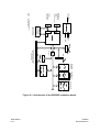
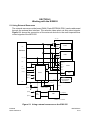
Technical Features of the EVB555
The following list summarizes the technical features of the EVB555 evaluation board.
The architecture of the board is displayed in Figure 2-1 on the following page.
• General advantages
— Full function range of the MPC555 can be used
— Microcontroller works with variable clock rate (up to 40 MHz)
• Memory
— Contains 1 Mbyte fast, synchronous SRAM (32-bit wide, burstable)
— 512 Kbyte external flash memory (32-bit wide, burstable)
• Configurability
— Convenient configuration of the PLL of the microcontroller
via a triple DIP switch
— Reset configuration of the MPC555 via a DIP switch (32 bits)
• Extensive analysis and debug support
— Flexible BDM interface (background debug mode) for debugging
— Direct connection to the ETAS emulator test probe ETKP-1
— Excellent analysis possibilities with 268-pin interface for
logic analyzers (6 AMP Mictor and 2 berg type connector)
— Connection of the probe to Lauterbach Trace32
emulation and programming system
• Very good expansion capability
— MAPI-400 interface
Interface as a connection to a customer-specific base-board
(user extension board)
— Customized communication expansion
Customer-specific expansion module, e.g. for CAN,
additional serial interfaces (RS232)
— Host communication expansion
Expansion module for high-speed communication to host system,
e.g. via Ethernet, Firewire
— Port replacement unit (PRU)
In ”external bus mode” 64 general purpose I/O pins are available
that are required by the MPC555 for the bus interface.
EVB555
Quick Reference
MOTOROLA
2-11
Power Supply
(7 .. 36 V)
Background
Debug Mode
(BDM)
(10-pin Connector)
(''SRZIVXIV
&
(
1
7
-
'
3,3 V
5V
:
14'
(272-pin BGA)
'%2
Customized
Communication
Expansion
(2x 20-pin Samtec
TFM-110-12-S-D-LC)
- Port Replacement Unit
- Emulator Probe
0SKMG%REP]^IV4SVX
\TMR%141MGXSV
GSRRIGXSV\TMR,4
TMS28F033
(PQFP-80)
2x MCM69F737
(TQFP-100)
FYVWXEFPI
/\
\
FYVWXEFPI
/\
6%1
0EYXIVFEGL
*PEWL
1F]XI
JSV+4-3kW
1IQSV]0SKMG469
/F]XI
7-7EQXIG
*8)+(:
Bus Switch
TMR7EQXIG
)8/'SRRIGXSV
830'750'
User Extension Board Connector
(5x 100-pin Robinson Nugent
P50L-100 S-BS)
(2x 60-pin Samtec
TFM-130-12-S-D-LC)
,SWX
)\TERWMSR
'SQQYRMGEXMSR
9%68*MVI[MVI
)XLIVRIX
Quick Reference
2-12
EVB555
MOTOROLA
RS232
(9-pin D-Sub
Connector)
PRU
ETK
Figure 2-1 Architecture of the EVB555 evaluation board
SECTION 3
Overview of the Evaluation Board
Figure 3-1 EVB555 Top
EVB555
Quick Reference
MOTOROLA
3-13
Figure 3-2 EVB555 Bottom
MOTOROLA
3-14
EVB555
Quick Reference
SECTION 4
-RXIVJEGIWERH'SRJMKYVEXMSR4SWWMFMPMXMIW
4.1 Power Supply
4.1.1 Supply Voltage Connection
The supply voltage should be connected using 2-wire line to the Power clamp
(CO102). Both solid as well as flexible wire can be used. The recommended diameter
is 0.5 to 2.5 mm2.
Observe polarity (+,-) and voltage range (7..36V)!
The current consumption at a supply voltage of 12 Volts is as follows (without external
load):
• Debug mode: 120 - 150mA
• Standby mode: 20 - 30mA
Additional current is required at startup and during high I/O activity.
4.1.2 Standby
After connecting the external supply voltage, the evaluation board is in standby mode.
Only the SRAMs and the standby power pin of the MPC555 are supplied with power.
The MPC555 is in reset. This mode is shown by the Standby Power LED (LD703,
yellow).
4.1.3 Power On
The toggle switch Power On (SW703) is used for activating the operating voltage of
the EVB555. The activated state is shown by the additional LED Power On (LD702,
green). All modules on the evaluation board are now supplied with power.
4.2 Single Chip/External Bus Mode
The MPC555 can be operated as a single-chip microcontroller or by using the external
bus interface (16-bit or 32-bit wide). The operating mode is set using the ”SC” bits in
the SIU module configuration register or in the hard reset configuration word (see
MPC555 Manual).
4.2.1 Single Chip Mode
The external resources on the evaluation board, such as SRAM, flash or port replacement unit (PRU), are not used. The pins, which have a second assignment to the
external bus interface are now available as general purpose I/O pins. The external bus
must be disconnected in this operating mode. Set the DIP switch ”ext. Bus” (SW1006) to ”Off” for this purpose.
EVB555
Quick Reference
MOTOROLA
4-15
4.2.2 External Bus Interface
The external bus makes it possible to use the resources of the EVB555, such as
SRAM, Flash-EEPROM or host communication expansion. The pins are used here for
addresses and data. Section 5.2. explains how the general purpose I/O lines are still
available on the EVB555.
4.3 BDM Interface
The basic debug interface of the EVB555 is the background debug mode interface
(BDM for short).
4.3.1 BDM Modes
Two variants are possible here for the support of the configurable use of the pins on
the MPC555:
Variant A - maximum debug capability
BDM pin
1
6
MPC555 signal
VFLS0_MPIO3
VFLS1_MPIO4
MPC555 pin
J18
K18
Variant B - maximum external bus capability
BDM pin
1
6
MPC555 pin
IWP0_VFLS0
IWP1_VFLS1
MPC555 pin
L2
L1
4.3.2 BDM/JTAG Support
Due to the double-use of the same pins on the MPC555 for the BDM and the JTAG
interface, only one of both interfaces can be used at the same time. The operating
mode is selected via the SW102 switch (BDM/Service). The relevant configuration of
the MPC555 is explained in the MPC555 User Manual.
• "BDM" setting
The BDM interface is available at the BDM connector (CO100) .
• "JTAG" setting
The JTAG interface is available at the Service connector (CO103). This is
required for test purposes (e.g. manufacture test) and for programming the EPLD.
The SW102 switch can always remain in the BDM setting when the EVB555 is operated normally.
MOTOROLA
4-16
EVB555
Quick Reference
4.4 Programming the Flash Modules
4.4.1 External Flash
A separate programming voltage of 12V is required for programming the external
Flash-EEPROM. This can be controlled and should not be connected permanently for
safety reasons.
• Manual control
The programming voltage Vpp12 can be activated with the DIP switch ”Vpp12 on”
(SW100-1). It is then permanently connected to the external flash. To protect the
flash memory from being overwritten by accident, the switch should be ”off” when
no programming is to take place.
• Automatic control
If the ”Vpp12 auto” option is enabled (SW100-2 on), the Vpp12 programming voltage can be switched on by the MPC555 program or by the connected ETAS
emulator test probe (ETK).
— Control by CPU program
Vpp12 is activated by entering ”1” in the programming voltage control register
(cf. Figure 5-2). Vpp12 is deactivated by entering a ”0” in the register.
— Control by the emulator test probe (ETK)
The ETK can activate the programming voltage by applying a high level at the
SGEPEE signal (CO508, pin 137). This makes it possible for the ETK to program the external flash.
4.4.2 Internal Flash of the MPC555
Two prerequisites must be fulfilled for programming the internal flash memory of the
MPC555:
1. Vpp5 (5 V) programming voltage is connected.
2. Programming is enabled by the high level at the EPEE pin.
The Vpp5 programming voltage can be applied separately by closing the ”Vpp5 on”
(SW100-3) DIP switch. To protect the internal flash from being overwritten by accident,
the switch should be ”off” when no programming is to take place.
Enabling programming via the EPEE pin
1. The pin can be permanently connected to a high level
with the ”EPEE” (SW100-4 on) switch
2. The ETK can enable the programming mode by a high level
at the SGEPEE signal (C0508, pin 137).
EVB555
Quick Reference
MOTOROLA
4-17
4.5 Interfaces for Testing and Debugging
4.5.1 Logic Analyzer Interface
The connection for the logic analyzer consists of 2 parts:
• digital signals: LA1 to LA6 (CO500 - 505) 38-pin AMP Mictor connector
• analog signals: LA7 and LA8 (CO506,507) 20-pin connector
The assignment of all Logic Analyzer interface connectors can be found in
Appendix A.2.
4.5.2 Trace32 Lauterbach
The CO509 connector is used for connecting the trace module of the Trace32 BDM
debugger (produced by Lauterbach Datentechnik GmbH). The functionality of the
debugger can be expanded in this way.
4.5.3 ETK Connector
The ETK connector (CO508) is used for connecting the ETKP-1 emulator test probe
(made by ETAS GmbH & Co.KG), which is widely used in automotive engineering.
The ETKP-1 is a memory emulator for 32-bit microcontroller systems and makes it
possible to access data in the external and internal memory of the microcontroller
while the program is running. That way, variables can be controlled and adapted at
program runtime. This procedure is used, for example, in the calibration of engine
ECUs in the automobile industry.
4.5.4 MAPI-400+100 Interface
The MAPI-400+100 interface makes it possible to expand the EVB555 with extensive
and customer-specific hardware. For example, there could be signal converters and
output drivers connected to extend the EVB555 to a test sample of a control unit for
industrial use.
The interface consists of two parts.
• MAPI-400 interface
The MAPI-400 interface (CO600 - CO603) is a standard interface for 32-bit microcontrollers made by Motorola. It makes all necessary signals, such as the address
and data bus, as well as control signals, available for the expansion of the microcontroller system. The interface consists of four 100-pin sockets (Robinson
Nugent P50L-100-S-BS-TGF). The assignment is shown in Appendix A.1.1.
• ”Port replacement unit” (PRU) connector
This connector (CO604, Robinson Nugent P50L-100-S-BS-TGF) extends the
MAPI-400 interface with signals of the port replacement unit (PRU). This means
that 64 general purpose I/O pins are again available in ”external bus mode” that
are required for the bus interface at the MPC555.
MOTOROLA
4-18
EVB555
Quick Reference
4.6 Reset and Reset Configuration
4.6.1 Reset Button
The Reset (SW702) button initiates a hard reset of the MPC555. When a hard reset
occurs, the MPC555 terminates the current program and enters the reset state. The
PLL continues to run, however. Once the button is released, the MPC555 starts to
work again by reading the system configuration (hard reset configuration).
4.6.2 Hard Reset Configuration
The hard reset configuration makes it possible to influence the behavior of the
MPC555 from outside. It particularly includes settings that are necessary before or
during the start of the first program. The reset configuration is read by the MPC555
after the supply voltage is switched on and after a hard reset has occurred.
Setting the hard reset configuration is conveniently solved on the EVB555 by assigning the hard reset configuration word via 32 DIP switches.
Table 4-1 on the following page is a short summary of the meaning of the individual
bits. For a more detailed description, please consult the MPC555 User Manual. The
specified variant makes it possible to work with a BDM debugger.
EVB555
Quick Reference
MOTOROLA
4-19
Bit
Name
0
EARB
1
IP
2
BDRV
3
BDIS
4:5
BPS
9:10
DBGC
11
DBPC
12
ATWC
13:14
EBDF
16
PRPM
17:18
SC
19
ETRE
20
FLEN
23
CLES
28:30
ISB
31
DME
Description
0: internal arbitration
1: external arbitration
Interrupt table location after reset
0: MSR(IP) =1
1: MSR(IP) =0
0: reduced drive strength of bus pins
1: full drive strength of bus pins
0: bank 0 is bootable
1: memory controller inactive
Boot port size
00: 32-bit
01: 8-bit
10: 16-bit
11: reserved
Debug pin configuration (IWP,BI,BG,BR,BB)
(6.13.1.1)
Debug pin configuration
0: BDM
1: JTAG
Address type <> Write enable
0: /WE
1: AT
External bus division factor
00: CLKOUT = GCLK2
01: CLKOUT = GCLK2/2
Peripheral mode enable
0: normal
1: external master
Single chip select
00: extended chip, 32-bit data
01: extended chip, 16-bit data
10: single chip, show cycle (address)
11: single chip
Extended table relocation
0: off
1: on
0: internal flash disabled (boot external)
1: internal flash enabled
0: little endian swap logic inactive
1: little endian swap logic active
Initial internal space base (6.12.1.2)
0: dual mapping disabled
1: dual mapping enabled
Var. 1
0
0
1
0
00
10
0
0
00
0
00
0
1
0
00
0
Table 4-1 Hard reset configuration word
MOTOROLA
4-20
EVB555
Quick Reference
'SRJMKYVEXMSRSJXLI400
The MPC555 can work with varying external clock generation. The configuration of the
microcontroller for the clock used takes place before the operating voltage is applied.
The MODCK setting makes it possible to configure the PLL of the MPC555. Only a few
of the possible settings are useful due to the design of the EVB555:
MODCK
1
2
0
1
1
0
1
0
1
1
1
1
3
0
0
1
0
1
LME
MF+1
Timing Reference
1
0
0
0
1
5
1
1
5
1
freq(OSCM) = 4 MHz, limb mode enabled
freqclkout(max) = freq(EXTCLK) , limp mode disabled
freqclkout(max) = freq(EXTCLK) , limp mode disabled
freq(EXTCLK) = 4 MHz, limp mode disabled
freqclkout=freq(EXTCLK) , limp mode enabled
Table 4-2 PLL configuration
Please consult the MPC555 User Manual for an explanation of the PLL function and
limp mode.
The standard setting for the evaluation board should be ”010”. The PLL works using
the quartz crystal assembled on the EVB555 (4 MHz) whereby the limp mode is
enabled.
EVB555
Quick Reference
MOTOROLA
4-21
MOTOROLA
4-22
EVB555
Quick Reference
SECTION 5
Working with the EVB555
5.1 Using External Resources
The external resources on the board (RAM, Flash-EEPROM, PRU) can be addressed
through the external bus interface. The selection takes place via chip select signals.
Figure 5-1 shows the connection of the external devices to the most important bus
control signals of the MPC555.
/SGF_SEL
/OE
Flash
/SGEOF
/SGCSF
/CS0
MPC555
/OE
/SGWCS
RAM
/WE[0:3]
/WE_AT[0:3]
/SGCSM
/CS3
/SGWE[0:3]
/SGCSF
1 1)
2
/CS1
ETK
/SGWCS
3
/SGOE
/CSR
RD_/WR
/SGEOF
/CSPB
TSIZ[0:1]
1 1)
EPLD
2
/SGCSR
3
Piggyback
RAM
A[8:15],
A[28:31]
D[0:7]
Host
Communication
Expansion
/SGHCE
/CS2
PDIR[0:7]
VCC3
/ExtBus
SW100-6
/WE[0:3]
/POE[A,B], /PLE[A,B]
/PRUOE, /PRUDIR
/OE
A[8:31]
Bus
Switch
D[0:31]
A_PIO[0:31],
A[8:31]
PRU
B_PIO[0:31]
D[0:31]
1)
default: 1-2 connected
Figure 5-1 Using external resources on the EVB 555
EVB555
Quick Reference
MOTOROLA
5-23
The Flash-EPROM is selected with chip select 0 (/CS0). Chip select 1 (/CS1) is partitioned by the EPLD in ranges for the external RAM, the PRU, the RAM extension on
the ETK and the Host Communication Expansion. This division takes place according
to addresses and is shown below.
Chip Select 1:
1 MB Address Space
Host Communication
Extension (HCE)
(HCE: /SGHCE)
1 MB RAM
at ETK Piggyback
(ETK: /SGCSR)
A8..A11: XX11
Vpp12 Control
0x 01 000C
Version Number
0x 01 0000
A8..A11: XX10
PRU
A8..A11: XX01
1 MB external RAM
PRU Data2
0x 00 0008
PRU Data1
0x 00 0004
PRU Configuration
0x 00 0000
(ETK: /SGWCS)
A8..A11: XX00
Chip Select 0:
1 MB external Flash
(ETK: /SGCSF)
Dual Mapping Area
for internal Flash or RAM
(ETK: /SGCSM)
Chip Select 3:
Figure 5-2 Overview of memory selection
The memory size assigned to chip select 1 (/CS1) of the MPC555 should therefore be
4 Mbyte. If the units intended for the higher addresses are not used, this area can also
be selected to be smaller (e.g. only 2 Mbyte for RAM and PRU).
MOTOROLA
5-24
EVB555
Quick Reference
5.2 Working with the PRU
The port replacement unit, PRU, provides 64 general purpose I/O lines to compensate
the loss of the I/O pins used for the external bus interface.
The EPLD controls the PRU and decodes the addresses for the two groups of I/O
channels (A_PIO[0..31] and B_PIO[0..31]). The direction (input or output) of the I/O
lines can be configured by setting the corresponding bits PRU_CONF register of the
EPLD (see Table 5-1). If a configuration bit is set to “0“ the port is used for output
whereas a value of "1" means that the port is used for input..
Configuration bit no.
0
1
2
3
4
5
6
7
I/O lines
A_PIO[24..31]
A_PIO[16..24]
A_PIO[8..15]
A_PIO[0..7]
B_PIO[24..31]
B_PIO[16..24]
B_PIO[8..15]
B_PIO[0..7]
Table 5-1 Allocation of the configuration bits
The value of an I/O line defined as input is read from address PRU_DATA1 (for
A_PIO[0..31]) or PRU_DATA2 (for B_PIO[0..31]). The EPLD drives the PRU to put the
values of all 32 bits per group on the bus.
For setting output values, data is written to address PRU_DATA1 or PRU_DATA2 and
latched to the output ports. If a PRU read operation follows, the previously written values are read in again from the ports working as outputs.
In Figure 5-3 the principle of the address decoding is shown.
A0
A7A8
external RAM
xx00
PRU
xx01
A15
0000
0000
0000
0001
0001
ETK Piggyback
xx10
Host
Communication
Extension
xx11
A28
A31
0000
0100
1000
0000
1100
PRU_CONF
PRU_DATA1
PRU_DATA2
EPLD Version
Vpp12 Control
Figure 5-3 Address decoding by EPLD
EVB555
Quick Reference
MOTOROLA
5-25
5.3 Notes on the External Flash Memory
The external flash memory, which is produced by Texas Instruments, has to be configured before you can read from it. This procedure is described in the data sheet of
the flash memory.
Internal clock
32MHz
40MHz
40MHz
Bus clock
32MHz
20MHz
40MHz
External flash usable
Yes
Yes
No
Table 5-2 External flash memory at different clock rates
The flash memory only works correctly at a bus clock rate of 33 MHz or less. The
resulting variants for the EVB555 are shown in Table 5-2.
5.4 Booting on the EVB555
To be able to start a program without a BDM debugger, it is necessary to boot from
non-volatile memory (i.e., from flash memory). The mode can be set via the reset configuration word (see Section 4.6.2.). There are a few points about the EVB555 that
should be observed.
The external flash memory cannot be used for booting since it does not provide a
mechanism for saving its start-up configuration. It has to be configured before you can
read from it.
Booting from the internal flash of the MPC555 is supported by the evaluation board.
Earlier versions of the MPC555 are not, however, capable of booting from the internal
flash at an internal clock rate of 20 MHz. The standard clock rate is 20 MHz, which is
generated by multiplying the crystal frequency (4 MHz) with the mode clock configuration factor 5.
You can solve this problem by exchanging the external crystal. It is recommended that
]SY VITPEGI XLI 1,^ GV]WXEP F] E 1,^ X]TI ERH STIVEXI XLI 400 SJ XLI
14'MR QSHI-RXLEXGEWI]SY[MPPIRHYT[MXLE 1,^VEXI8LIZEPYI
SJXLIQSHIGPSGO has to be changed to ”011” for this purpose 7IGXMSR ). This
mode is within the PLL specification and even earlier versions of the MPC555 should
boot reliably from internal flash memory. If you want to operate the board in this way
long-term, you should reduce the capacitor at the XFC output (C201) to 560 pF.
MOTOROLA
5-26
EVB555
Quick Reference
APPENDIX A
Connector Assignment
The following tables display the connector assignment of the EVB555 evaluation
board. Only the connected pins are listed; all other pins are open.
EVB555
Quick Reference
MOTOROLA
A-27
A.1 MAPI-400+100 Interface
A.1.1 MAPI0 Interface Assignment
A.1.1.1 Assignment of J1/P1 (CO600) connector:
Pin
MPC pin
Signal name
1
3
5
7
9
11
13
15
17
27
29
30
31
32
33
35
36
37
38
39
42
43
44
45
47
48
49
50
51
53
54
55
56
57
C9
A10
B10
A11
D10
C10
B11
D11
C11
D3
A2
E17
D4
D18
C3
A3
D19
D5
D20
B3
F17
C4
E18
A4
C5
F18
B4
E19
B5
A5
A6
C6
C2
B6
AAN51_PQB7
AAN52_PQA0
AAN53_PQA1
AAN54_PQA2
AAN55_PQA3
AAN56_PQA4
AAN57_PQA5
AAN58_PQA6
AAN59_PQA7
A_TPUCH0
A_TPUCH1
MPWM0
A_TPUCH2
MPWM1
A_TPUCH3
A_TPUCH4
MPWM2
A_TPUCH5
MPWM3
A_TPUCH6
MPWM16
A_TPUCH7
MPWM17
A_TPUCH8
A_TPUCH9
MPWM18
A_TPUCH10
MPWM19
A_TPUCH11
A_TPUCH12
A_TPUCH15
A_TPUCH13
A_T2CLK
A_TPUCH14
61
M2
/IRQ1B_SGP
62
M1
/IRQ0B_SGP
63
L3
/IRQ3B_SGP
64
M3
/IRQ2B_SGP
65
W18
/IRQ5B_SGP
66
L4
/IRQ4B_SGP
MOTOROLA
A-28
Description corresponding to data sheet
See AAN48_PQB4
Analog input: passed on as a separate signal to the QADC.
See AAN52_PQA0
See AAN52_PQA0
See AAN52_PQA0
See AAN52_PQA0
See AAN52_PQA0
See AAN52_PQA0
See AAN52_PQA0
A_TPUCH0 - A_TPUCH15: Time Processor Unit A channel
See A_TPUCH0
MPWM0 - MPWM3, MPWM16 - MPWM19: Pulse width modulation
See A_TPUCH0
See MPWM0
See A_TPUCH0
See A_TPUCH0
See MPWM0
See A_TPUCH0
See MPWM0
See A_TPUCH0
See MPWM0
See A_TPUCH0
See MPWM0
See A_TPUCH0
See A_TPUCH0
See MPWM0
See A_TPUCH0
See MPWM0
See A_TPUCH0
See A_TPUCH0
See A_TPUCH0
See A_TPUCH0
to clock or gate the timer count register 2 (TCR2) within the TPU.
See A_TPUCH0
Interrupt request, SGPIO, reservation:
to indicate that the internal core initiated a transfer.
Interrupt request, SGPIO
Interrupt request, SGPIO, kill reservation,
retry: indicates to a master that the cycle is terminated
but should be repeated.
Interrupt request, SGPIO, cancel reservation: to clear its reservation.
Interrupt request, SGPIO, mode clock [1]:
sampled at the negation of /PORESET in order to
configure the PLL/clock mode.
Interrupt request, SGPIO, address type:
indicates one of the 16 ”address types”. The address type signals are
valid at the rising edge of the clock in which the special transfer start
(STS) is asserted.
EVB555
Quick Reference
Pin
MPC pin
Signal name
67
Y19
/IRQ7B_mck3
68
Y18
/IRQ6B_mck2
100
P17
VPP
28, 41,
46, 71,
74, 89,
92
EVB555
Quick Reference
GND
Description corresponding to data sheet
Interrupt request, mode clock [3]:
similar to IRQ5B, no SGPIO
Interrupt request, mode clock [2]:
similar to IRQ5B, no SGPIO
Flash supply voltage (5V) used during program and erase operation of
the CMF.
Ground
MOTOROLA
A-29
A.1.1.2 Assignment of J2/P2 (CO601) connector:
Pin
2
4
MPC pin
D9
B9
Signal name
AAN50_PQB6
AAN49_PQB5
6
A9
AAN48_PQB4
8
10
12
B8
C8
AAN3_PQB3
AAN2_PQB2
14
A8
AAN0_PQB0
21
A17
MDA11
22
23
24
25
26
27
28
A18
A19
B17
B18
C17
B20
C18
MDA12
MDA13
MDA14
MDA15
MDA27
MDA28
MDA29
30
W20
/HRESETB
31
C16
ETRIG1
32
U18
EXTCLK
33
B16
ETRIG2
34
N4
/BBB_IWP3
35
U4
/BDIPB
36
N3
/BGB_LWP1
37
V2
/BIB_/STSB
38
N2
/BRB_IWP2
39
40
41
42
47
V1
M4
U3
P18
M19
/BURSTB
SGP_/IRQOUTB
/TSB
EPEE
ECK
48
U19
ENGCLK/BUCLK
49
50
51
52
61
65
66
67
N17
N18
N19
N20
C19
C20
G17
E20
RXD1_QGPI
TXD1_QGPO
RXD2_QGPI
TXD2_QGPO
MDA30
MDA31
MPIO5
MPIO6
MOTOROLA
A-30
Description corresponding to the data sheet
See AAN48_PQB4
See AAN48_PQB4
Analog input channel: passed on as a separate signal to the QADC.
Port (PQB): has a synchronizer with an input enable and clock.
See AAN0_PQB0
See AAN0_PQB0
See AAN0_PQB0
Multiplexed input analog channel: passed on as a
separate signal to the QADC.
Double action: provide a path for two 16-bit input captures
and two 16-bit output captures.
See MDA11
See MDA11
See MDA11
See MDA11
See MDA11
See MDA11
See MDA11
Hard reset: after negation of /HRESET is detected, a 16-cycle period is
taken before testing an external reset. An external pull-up device is
required to negate /HRESET.
External trigger input to the QADC_A and QADC_B modules.
Can be configured for both QADC_A and QADC_B.
External frequency source for the chip.
Must be grounded if unused.
See ETRIG1
Bus busy: master is using the bus.
Visible instruction queue flush status.
Load/store watchpoint. 3
Burst data in progress: indicates that a data beat follows the current one.
Bus grant: indicates external data bus status. Visible instruction
queue flush status Load/store watchpoint
Burst inhibit: ”0” → slave device is not able to support burst transfers.
Special transfer start: beginning of an internal transaction in showcycle
mode.
Bus request: the data bus has been requested for external cycle.
Visible instruction queue flush status Load/store watchpoint 2
Burst indicator: ”0” → burst transaction
SGPIO, interrupt out: an interrupt has been sent to external devices.
Transfer start: start of a bus cycle that transfers data
Input: will externally control the program or erase operations.
External bus clock (EBCK): external baud clock used by SCI1 and SCI2
ENGCLK: engineering clock output. Full strength, half strength, disabled.
Using EECLK[0:1] bits in the SCCR register.
BUCLK: backup clock, less precise on-chip ring oscillator for minimum
functionality.
Receive data: serial input from the SCI1
Transmit data: serial output from the SCI1
Receive data: serial input from the SCI2
Transmit data: serial output from the SCI2
See MDA11
See MDA11
GPIO
GPIO
EVB555
Quick Reference
Pin
68
69
70
71
72
73
74
75
76
88
90
92
94
96
98
100
17, 18,
43, 46,
63, 64,
83, 84
MPC pin
F19
G18
F20
H17
G19
G20
H20
H19
H18
A12
B12
A13
A14
B13
C12
D12
EVB555
Quick Reference
Signal name
MPIO7
MPIO8
MPIO9
MPIO10
MPIO11
MPIO12
MPIO13
MPIO14
MPIO15
BAN0_PQB0
BAN1_PQB1
BAN2_PQB2
BAN3_PQB3
BAN48_PQB4
BAN49_PQB5
BAN50_PQB6
Description corresponding to the data sheet
GPIO
GPIO
GPIO
GPIO
GPIO
GPIO
GPIO
GPIO
GPIO
See AAN0_PQB0
See AAN0_PQB0
See AAN0_PQB0
See AAN0_PQB0
See AAN48_PQB4
See AAN48_PQB4
See AAN48_PQB4
GND
Ground
MOTOROLA
A-31
A.1.1.3 %WWMKRQIRXSJ.4'3GSRRIGXSV
Pin
2
4
6
8
10
12
14
16
18
26
27
28
29
30
32
33
34
35
36
38
MPC pin
A15
B14
C13
B15
D13
C14
C15
D14
D15
H2
K20
H1
K19
G1
G2
H3
G3
H4
F1
F2
Signal name
BAN51_PQB7
BAN52_PQA0
BAN53_PQA1
BAN54_PQA2
BAN55_PQA3
BAN56_PQA4
BAN57_PQA5
BAN58_PQA6
BAN59_PQA7
B_TPUCH0
A_CNRX0
B_TPUCH1
A_CNTX0
B_TPUCH2
B_TPUCH3
B_CNRX0
B_TPUCH4
B_CNTX0
B_TPUCH5
B_TPUCH6
39
M20
SCK_QGP6
40
E1
B_TPUCH7
41
L19
MISO_QGP4
42
44
F3
G4
B_TPUCH8
B_TPUCH9
45
L20
MOSI_QGP5
46
E2
B_TPUCH10
47
L18
PCS0_QGP
48
50
D1
F4
B_TPUCH11
B_TPUCH12
51
L17
PCS1_QGP
52
53
54
56
57
58
D2
M18
E3
C1
M17
B1
B_TPUCH13
PCS2_QGP
B_TPUCH14
B_TPUCH15
PCS3_QGP
B_T2CLK
62
J19
VF0_MPIO0
64
66
J20
J17
VF1_MPIO1
VF2_MPIO2
67
J18
VFLS0_MPIO3
69
K18
VFLS1_MPIO4
71
L2
IWP0_VFLS
73
L1
IWP1_VFLS
MOTOROLA
A-32
Description corresponding to the data sheet
See AAN48_PQB4
See AAN52_PQA0
See AAN52_PQA0
See AAN52_PQA0
See AAN52_PQA0
See AAN52_PQA0
See AAN52_PQA0
See AAN52_PQA0
See AAN52_PQA0
B_TPUCH0 - B_TPUCH15: Time Processor Unit B channel
TOUCAN receive data 0: serial data input
See B_TPUCH0
TOUCAN transmit data 0: serial data output
See B_TPUCH0
See B_TPUCH0
TOUCAN receive data 0: serial data input
See B_TPUCH0
TOUCAN transmit data 0: serial data output
See B_TPUCH0
See B_TPUCH0
SCK: provides the clock from the QSPI in master mode or to the QSPI in
slave mode
See B_TPUCH0
Master-in slave-out (MISO): provides serial data input to the QSPI in
master mode and serial data output from the QSPI in slave mode
See B_TPUCH0
See B_TPUCH0
Master-out slave-in (MOSI): provides serial data output to the QSPI in
master mode, and serial data input from the QSPI in slave mode.
See B_TPUCH0
PCS0: provide QSPI peripheral chip select 0.
SS: places the QSPI in slave mode.
QSPI GPIO[0]: can be configured as GPIO if not needed.
See B_TPUCH0
See B_TPUCH0
PCS1: provide QSPI peripheral chip select 1.
QSPI GPIO[1]: can be configured as GPIO if not needed.
See B_TPUCH0
See PCS1_QGP
See B_TPUCH0
See B_TPUCH0
See PCS1_QGP
See A_T2CLK
VF[0:2] visible instruction queue flush status: output by the chip when program instruction flow tracking is required. GPIO
See VF0_MPIO0
See VF0_MPIO0
Visible history buffer flush status: to allow program instruction flow
tracking.
See VFLS0_MPIO3
Instruction watchpoint. Visible history buffer flush status: output by the
chip to enable program instruction flow tracking.
See IWP0_VFLS
EVB555
Quick Reference
Pin
MPC pin
Signal name
77
V19
/PORESETB
80
J2
TDO_DSDO
82
K2
TDI_DSDI
83
85
86
87
88
K1
J1
U1
J3
T3
TMS
TCK_DSCK
TSIZ0
/TRSTB
TSIZ1
89
V20
/SRESETB
90
U17
/RSTCONF_TEXP
94
K3
FRZ_/PTR
25, 43,
65, 68,
81, 91,
95, 97
EVB555
Quick Reference
GND
Description corresponding to the data sheet
Power on reset: activated as a result of a voltage failure. The internal /
PORESET is asserted only if /PORESET is asserted > 100 ns.
Test data out, development serial data output:
the data-out line of the debug port interface.
Test data in, development serial data input :
The data-in line for the debug port interface.
Test mode select
Test clock, development serial clock: clock for the debug interface.
Transfer size: indicates the size of the requested data transfer.
Test reset: asynchronous reset to the test logic.
Transfer size: indicates the size of the requested data transfer.
Soft reset: after negation of /SRESET is detected, a 16-cycle period is
taken before testing an external reset. An external pull-up device is
required to negate /SRESET.
Reset configuration (input): the reset configuration mode will be sampled
from the external data bus.
Timer expired (output): status of the TEXPS bit in the PLPRCR register in
the USIU.
SGPIO freeze: RCPU is in debug mode
program trace (/PTR): an instruction fetch is taking place.
Ground
MOTOROLA
A-33
A.1.1.4 %WWMKRQIRXSJ.4'3GSRRIGXSV
Pin
MPC pin
Signal name
3
W9
Data_SGP1
4
5
6
7
8
9
10
11
12
13
14
17
18
19
20
21
22
23
24
25
26
29
30
31
32
33
34
35
36
37
38
Y9
W10
Y10
W11
Y11
W12
Y12
W13
Y13
W14
Y14
W15
Y15
W16
Y16
W17
Y17
V16
V17
V15
U16
U14
V14
U13
V13
U12
V12
U11
V11
V9
V10
Data_SGP0
Data_SGP3
Data_SGP2
Data_SGP5
Data_SGP4
Data_SGP7
Data_SGP6
Data_SGP9
Data_SGP8
Data_SGP11
Data_SGP10
Data_SGP13
Data_SGP12
Data_SGP15
Data_SGP14
Data_SGP17
Data_SGP16
Data_SGP19
Data_SGP18
Data_SGP21
Data_SGP20
Data_SGP23
Data_SGP22
Data_SGP25
Data_SGP24
Data_SGP27
Data_SGP26
Data_SGP29
Data_SGP28
Data_SGP31
Data_SGP30
MOTOROLA
A-34
Description corresponding to the data sheet
Data_SGP0 - Data_SGP31:
can be sized to support 8-, 16-, 24- or 32-bit transfers.
Data_SGP0 is the MSB.
EVB555
Quick Reference
Pin
49
50
51
52
53
54
55
56
59
60
61
62
63
64
65
66
67
68
69
70
71
72
73
74
77
78
MPC pin
V5
V6
V3
V4
Y2
W1
Y3
W3
Y4
W4
Y5
W5
Y6
W6
W7
V7
Y8
Y7
V8
W8
U9
U8
U6
U7
U2
T2
Signal name
Addr_SGP9
Addr_SGP8
Addr_SGP11
Addr_SGP10
Addr_SGP13
Addr_SGP12
Addr_SGP15
Addr_SGP14
Addr_SGP17
Addr_SGP16
Addr_SGP19
Addr_SGP18
Addr_SGP21
Addr_SGP20
Addr_SGP23
Addr_SGP22
Addr_SGP25
Addr_SGP24
Addr_SGP27
Addr_SGP26
Addr_SGP29
Addr_SGP28
Addr_SGP31
Addr_SGP30
/TAB
/TEAB
80
N1
/WEB_AT[0]
81
R1
RD_/WRB
82
P1
/WEB_AT[1]
84
P2
/WEB_AT[2]
85
P4
/CS0B
86
P3
/WEB_AT[3]
87
88
89
91
95
15, 16,
27, 28,
39, 40,
57, 58,
75, 76,
83, 93,
96 ,97
R4
T1
R3
R2
V18
/CS1B
/OEB
/CS2B
/CS3B
CLKOUT
Transfer acknowledge: transfer accepted/valid
Transfer error acknowledge: error occurred in the current transaction
Write enable: /WE0 is asserted if the data lane DATA[0:7]
contains valid data.
Read/write : ”1” → read, ”0” → write
Write enable: /WE1 is asserted if the data lane DATA[8:15]
contains valid data.
Write enable: /WE2 is asserted if the data lane DATA[16:23]
contains valid data.
Chip select: /CS0 can be the global chip select for the boot device.
Write enable: /WE3 is asserted if the data lane DATA[24:31]
contains valid data.
Chip select
Output enable
Chip select
Chip select
Clock out: can be configured to full strength, half strength or disabled.
GND
Ground
EVB555
Quick Reference
Description corresponding to the data sheet
Addr_SGP8 - Addr_SGP31:
24 address lines,
16 MB address space
MOTOROLA
A-35
The following connections are not on the MAPI 400 interface.
MPC pin
Signal name
U20
XTAL
T20
EXTAL
R19
R20
T19
B7
A7
T18
XFC
VDDSYN
VSSSYN
VRH
VRL
KAPWR
Description corresponding to the data sheet
Connection to an external crystal for the internal oscillator circuitry.
Connection to an external crystal for the internal oscillator.
Must be grounded, if unused.
External filter capacity: for an external capacitor filter for the PLL circuitry.
Power supply of the PLL circuitry
Power supply of the PLL circuitry
High reference voltage for QADC_A and QADC_B.
Low reference voltage for QADC_A and QADC_B.
Keep alive power: 3V supply for the SRAM.
A.1.2 PRU connector (CO604) assignment
Pin
Signal name
1
B_PIO0
2
A_PIO0
3
4
5
6
7
8
9
10
11
12
13
14
17
18
19
20
21
22
23
24
25
26
29
30
31
32
33
34
35
36
37
38
39
B_PIO1
A_PIO1
B_PIO2
A_PIO2
B_PIO3
A_PIO3
B_PIO4
A_PIO4
B_PIO5
A_PIO5
B_PIO6
A_PIO6
B_PIO7
A_PIO7
B_PIO8
A_PIO8
B_PIO9
A_PIO9
B_PIO10
A_PIO10
B_PIO11
A_PIO11
B_PIO12
A_PIO12
B_PIO13
A_PIO13
B_PIO14
A_PIO14
B_PIO15
A_PIO15
B_PIO16
A_PIO16
B_PIO17
MOTOROLA
A-36
Description corresponding to the data sheet
B_PIO0 - B_PIO31: second group of 32 General Purpose I/O lines
operated by the Port Replacement Unit
A_PIO0 - A_PIO31: first group of 32 General Purpose I/O lines
operated by the Port Replacement Unit
See B_PIO0
See A_PIO0
See B_PIO0
See A_PIO0
See B_PIO0
See A_PIO0
See B_PIO0
See A_PIO0
See B_PIO0
See A_PIO0
See B_PIO0
See A_PIO0
See B_PIO0
See A_PIO0
See B_PIO0
See A_PIO0
See B_PIO0
See A_PIO0
See B_PIO0
See A_PIO0
See B_PIO0
See A_PIO0
See B_PIO0
See A_PIO0
See B_PIO0
See A_PIO0
See B_PIO0
See A_PIO0
See B_PIO0
See A_PIO0
See B_PIO0
See A_PIO0
See B_PIO0
EVB555
Quick Reference
Pin
40
41
42
43
44
45
46
47
48
49
50
51
52
53
54
55
56
59
60
61
62
63
64
65
66
67
68
69
70
71
72
85
86
95, 96,
97, 98,
99, 100
15, 16,
27, 28,
39, 40,
57, 58,
75, 76,
83, 89,
90, 91,
92, 93,
94
Signal name
A_PIO17
B_PIO18
A_PIO18
B_PIO19
A_PIO19
B_PIO20
A_PIO20
B_PIO21
A_PIO21
B_PIO22
A_PIO22
B_PIO23
A_PIO23
B_PIO24
A_PIO24
B_PIO25
A_PIO25
B_PIO26
A_PIO26
B_PIO27
A_PIO27
B_PIO28
A_PIO28
B_PIO29
A_PIO29
B_PIO30
A_PIO30
B_PIO31
A_PIO31
B_PIO0
A_PIO0
/EXTBUS
STANDBY
Description corresponding to the data sheet
See A_PIO0
See B_PIO0
See A_PIO0
See B_PIO0
See A_PIO0
See B_PIO0
See A_PIO0
See B_PIO0
See A_PIO0
See B_PIO0
See A_PIO0
See B_PIO0
See A_PIO0
See B_PIO0
See A_PIO0
See B_PIO0
See A_PIO0
See B_PIO0
See A_PIO0
See B_PIO0
See A_PIO0
See B_PIO0
See A_PIO0
See B_PIO0
See A_PIO0
See B_PIO0
See A_PIO0
See B_PIO0
See A_PIO0
See B_PIO0
See A_PIO0
disconnect external resources from processor bus
switch EVB into Stanby mode
UB2
alternative power supply path
GND
Ground
EVB555
Quick Reference
MOTOROLA
A-37
A.2 Assignment of Logic Analyzer Interface
A.2.1 %WWMKRQIRXSJ'3GSRRIGXSV
Pin no.
6
8
10
12
14
16
18
20
22
24
26
28
30
32
34
36
38
LA channel
Clk
D15
D14
D13
D12
D11
D10
D9
D8
D7
D6
D5
D4
D3
D2
D1
D0
Label
STAT
ADDR
ADDR
ADDR
ADDR
ADDR
ADDR
ADDR
ADDR
ADDR
ADDR
ADDR
ADDR
ADDR
ADDR
ADDR
ADDR
Sgnal name
CLKOUT
A[16]
A[17]
A[18]
A[19]
A[20]
A[21]
A[22]
A[23]
A[24]
A[25]
A[26]
A[27]
A[28]
A[29]
A[30]
A[31]
MPC pin
V18
W4
Y4
W5
Y5
W6
Y6
V7
W7
Y7
Y8
W8
V8
U8
U9
U7
U6
MPC signal name
CLKOUT
Addr_SGP16
Addr_SGP17
Addr_SGP18
Addr_SGP19
Addr_SGP20
Addr_SGP21
Addr_SGP22
Addr_SGP23
Addr_SGP24
Addr_SGP25
Addr_SGP26
Addr_SGP27
Addr_SGP28
Addr_SGP29
Addr_SGP30
Addr_SGP31
5
7
Clk
D15
STAT
/TS
/PORESET
U3
V19
9
D14
KAPWR
11
13
15
17
19
21
23
25
27
29
31
33
35
37
D13
D12
D11
D10
D9
D8
D7
D6
D5
D4
D3
D2
D1
D0
EXTCLK
Test point 500
/CS[0]
/CS[1]
/CS[2]
/CS[3]
A[8]
A[9]
A[10]
A[11]
A[12]
A[13]
A[14]
A[15]
U18
/TSB
/PORESETB
Not to MPC555,
direct to VSTBY3_3
EXTCLK
P4
R4
R3
R2
V6
V5
V4
V3
W1
Y2
W3
Y3
/CS0B
/CS1B
/CS2B
/CS3B
Addr_SGP8
Addr_SGP9
Addr_SGP10
Addr_SGP11
Addr_SGP12
Addr_SGP13
Addr_SGP14
Addr_SGP15
MOTOROLA
A-38
ADDR
ADDR
ADDR
ADDR
ADDR
ADDR
ADDR
ADDR
ADDR
ADDR
ADDR
ADDR
EVB555
Quick Reference
A.2.2 Assignment of CO501 connector
Pin no.
6
8
10
12
14
16
18
20
22
24
26
28
30
32
34
36
38
LA channel
Clk
D15
D14
D13
D12
D11
D10
D9
D8
D7
D6
D5
D4
D3
D2
D1
D0
Label
STAT
DATA
DATA
DATA
DATA
DATA
DATA
DATA
DATA
DATA
DATA
DATA
DATA
DATA
DATA
DATA
DATA
Signal name
/TA
D[16]
D[17]
D[18]
D[19]
D[20]
D[21]
D[22]
D[23]
D[24]
D[25]
D[26]
D[27]
D[28]
D[29]
D[30]
D[31]
MPC pin
U2
Y17
W17
V17
V16
U16
V15
V14
U14
V13
U13
V12
U12
V11
U11
V10
V9
MPC signal name
/TAB
Data_SGP16
Data_SGP17
Data_SGP18
Data_SGP19
Data_SGP20
Data_SGP21
Data_SGP22
Data_SGP23
Data_SGP24
Data_SGP25
Data_SGP26
Data_SGP27
Data_SGP28
Data_SGP29
Data_SGP30
Data_SGP31
5
7
9
11
13
15
17
19
21
23
25
27
29
31
33
35
37
Clk
D15
D14
D13
D12
D11
D10
D9
D8
D7
D6
D5
D4
D3
D2
D1
D0
STAT
DATA
DATA
DATA
DATA
DATA
DATA
DATA
DATA
DATA
DATA
DATA
DATA
DATA
DATA
DATA
DATA
/STS
D[0]
D[1]
D[2]
D[3]
D[4]
D[5]
D[6]
D[7]
D[8]
D[9]
D[10]
D[11]
D[12]
D[13]
D[14]
D[15]
V2
Y9
W9
Y10
W10
Y11
W11
Y12
W12
Y13
W13
Y14
W14
Y15
W15
Y16
W16
/BIB_/STSB
Data_SGP0
Data_SGP1
Data_SGP2
Data_SGP3
Data_SGP4
Data_SGP5
Data_SGP6
Data_SGP7
Data_SGP8
Data_SGP9
Data_SGP10
Data_SGP11
Data_SGP12
Data_SGP13
Data_SGP14
Data_SGP15
EVB555
Quick Reference
MOTOROLA
A-39
A.2.3 Assignment of CO502 connector
Pin no.
6
8
10
12
14
16
18
20
22
24
26
28
30
32
34
36
38
LA channel
Clk
D15
D14
D13
D12
D11
D10
D9
D8
D7
D6
D5
D4
D3
D2
D1
D0
Label
STAT
STAT
STAT
STAT
STAT
STAT
STAT
STAT
STAT
STAT
STAT
STAT
STAT
STAT
STAT
STAT
STAT
Signal name
/TEA
/BURST
/BDIP
/OE
/WE[0]
/WE[1]
/WE[2]
/WE[3]
AT[2]
TSIZ[0]
TSIZ[1]
VFLS[0]
VFLS[1]
FRZ_/PTR
/RETRY
/SRESET
/HRESET
MPC pin
T2
V1
U4
T1
N1
P1
P2
P3
L4
U1
T3
J18
K18
K3
L3
V20
W20
MPC signal name
/TEAB
/BURSTB
/BDIPB
/OEB
/WEB_AT[0]
/WEB_AT[1]
/WEB_AT[2]
/WEB_AT[3]
/IRQ4B_SGP
TSIZ0
TSIZ1
VFLS0_MPIO3
VFLS1_MPIO4
FRZ_/PTR
/IRQ3B_SGP
/SRESETB
/HRESETB
5
7
9
11
13
15
17
19
21
23
25
27
29
31
33
35
36
Clk
D15
D14
D13
D12
D11
D10
D9
D8
D7
D6
D5
D4
D3
D2
D1
D0
STAT
RD_/WR
/CR
KR
/RSTCONF
IWP[0]
IWP[1]
IWP[2]
IWP[3]
LWP[0]
LWP[1]
DSCK
DSDO
DSDI
R1
M3
M2
U17
L2
L1
N2
N4
M4
N3
J1
J2
K2
RD_/WRB
/IRQ2B_SGP
/IRQ1B_SGP
/RSTCONF_TEXP
IWP0_VFLS
IWP1_VFLS
/BRB_IWP2
/BBB_IWP3
SGP_/IRQOUTB
/BGB_LWP1
TCK_DSCK
TDO_DSDO
TDI_DSDI
Compression pin 1)
VF[0]
VF[1]
VF[2]
J19
J20
J17
VF0_MPIO0
VF1_MPIO1
VF2_MPIO2
STAT
STAT
STAT
STAT
STAT
STAT
STAT
1) designated to be used in future by HP
MOTOROLA
A-40
EVB555
Quick Reference
A.2.4 Assignment of CO503 connector
Pin no.
6
8
10
12
14
16
18
20
22
24
26
28
30
32
34
36
38
LA channel Label
Clk
D15
D14
D13
D12
D11
D10
D9
D8
D7
D6
D5
D4
D3
D2
D1
D0
Signal name
SCK_QGPIO[6]
PCS[0]_/SS_QGPIO[0]
PCS[1]_QGPIO[1]
PCS[2]_QGPIO[2]
PCS[3]_QGPIO[3]
MISO_QGPIO[4]
MOSI_QGPIO[5]
TXD[1]_QGPO[1]
TXD[2 ]_QGPO[2]
RXD[1]_QGPI[1]
RXD[2]_QGPI[2]
MDA[4] (DA0)
MDA[5] (DA1)
MDA[6] (DA2)
MDA[7] (DA3)
MDA[8] (DA4)
n.c.
5
7
9
11
13
15
17
19
21
23
25
27
29
31
33
35
37
Clk
D15
D14
D13
D12
D11
D10
D9
D8
D7
D6
D5
D4
D3
D2
D1
D0
ECK
MDA[9] (DA5)
MDA[10] (DA6)
MDA[11] (DA7)
MDA[12] (DA8)
MDA[13] (DA9)
MPWM[14] (PWM0)
MPWM[15] (PWM1)
MPWM[16] (PWM2)
MPWM[17] (PWM3)
MPWM[18] (PWM4)
MPWM[19] (PWM5)
MPWM[20] (PWM6)
MPWM[21] (PWM7)
Test point 501
Test point 502
Test point 503
EVB555
Quick Reference
MPC pin
M20
L18
L17
M18
M17
L19
L20
N18
N20
N17
N19
A17
A18
A19
B17
B18
MPC signal name
SCK_QGP6
PCS0_QGP
PCS1_QGP
PCS2_QGP
PCS3_QGP
MISO_QGP4
MOSI_QGP5
TXD1_QGPO
TXD2_QGPO
RXD1_QGPI
RXD2_QGPI
MDA11
MDA12
MDA13
MDA14
MDA15
C17
B20
C18
C19
C20
E17
D18
D19
D20
F17
E18
F18
E19
ECK
MDA27
MDA28
MDA29
MDA30
MDA31
MPWM0
MPWM1
MPWM2
MPWM3
MPWM16
MPWM17
MPWM18
MPWM19
MOTOROLA
A-41
A.2.5 Assignment of CO504 connector
Pin no.
6
8
10
12
14
16
18
20
22
24
26
28
30
32
34
36
38
LA channel
Clk
D15
D14
D13
D12
D11
D10
D9
D8
D7
D6
D5
D4
D3
D2
D1
D0
5
7
9
11
13
15
17
19
21
23
25
27
29
31
33
35
37
Clk
D15
D14
D13
D12
D11
D10
D9
D8
D7
D6
D5
D4
D3
D2
D1
D0
MOTOROLA
A-42
Label
Signal name
ENGCLK_BUCLK
MGPIO[0]
MGPIO[1]
MGPIO[2]
MGPIO[3]
MGPIO[4]
MGPIO[5]
MGPIO[6]
MGPIO[7]
MGPIO[8]
MGPIO[9]
MGPIO[10]
MGPIO[11]
MGPIO[12]
MGPIO[13]
MGPIO[14]
MGPIO[15]
MPC pin
U19
J19
J20
J17
J18
K18
G17
E20
F19
G18
F20
H17
G19
G20
H20
H19
H18
MPC signal name
ENGCLK_BUCLK
VF0_MPIO0
VF1_MPIO1
VF2_MPIO2
VFLS0_MPIO3
VFLS1_MPIO4
MPIO5
MPIO6
MPIO7
MPIO8
MPIO9
MPIO10
MPIO11
MPIO12
MPIO13
MPIO14
MPIO15
T2CLK
TPU_A
TPUCH[0] TPU_A
TPUCH[1] TPU_A
TPUCH[2] TPU_A
TPUCH[3] TPU_A
TPUCH[4] TPU_A
TPUCH[5] TPU_A
TPUCH[6] TPU_A
TPUCH[7] TPU_A
TPUCH[8] TPU_A
TPUCH[9] TPU_A
TPUCH[10] TPU_A
TPUCH[11] TPU_A
TPUCH[12] TPU_A
TPUCH[13] TPU_A
TPUCH[14] TPU_A
TPUCH[15] TPU_A
C2
D3
A2
D4
C3
A3
D5
B3
C4
A4
C5
B4
B5
A5
C6
B6
A6
A_T2CLK
A_TPUCH0
A_TPUCH1
A_TPUCH2
A_TPUCH3
A_TPUCH4
A_TPUCH5
A_TPUCH6
A_TPUCH7
A_TPUCH8
A_TPUCH9
A_TPUCH10
A_TPUCH11
A_TPUCH12
A_TPUCH13
A_TPUCH14
A_TPUCH15
EVB555
Quick Reference
A.2.6 Assignment of CO505 connector
Pin no.
6
8
10
12
14
16
18
20
22
24
26
28
30
32
34
36
38
LA channel
Clk
D15
D14
D13
D12
D11
D10
D9
D8
D7
D6
D5
D4
D3
D2
D1
D0
5
7
9
11
13
15
17
Clk
D15
D14
D13
D12
D11
D10
19
D9
21
23
25
27
29
31
33
35
37
D8
D7
D6
D5
D4
D3
D2
D1
D0
EVB555
Quick Reference
Label
Signal name
T2CLK
TPU_B
TPUCH[0] TPU_B
TPUCH[1] TPU_B
TPUCH[2] TPU_B
TPUCH[3] TPU_B
TPUCH[4] TPU_B
TPUCH[5] TPU_B
TPUCH[6] TPU_B
TPUCH[7] TPU_B
TPUCH[8] TPU_B
TPUCH[9] TPU_B
TPUCH[10] TPU_B
TPUCH[11] TPU_B
TPUCH[12] TPU_B
TPUCH[13] TPU_B
TPUCH[14] TPU_B
TPUCH[15] TPU_B
n.c.
CNTX0_A
CNRX0_A
CNTX0_B
CNRX0_B
EPEE
/IRQ[0]_SGPIOC[0]
/IRQ[5]_SGPIOC[5]_
MODCK[1]
/IRQ[6]_MODCK[2]
/IRQ[7]_MODCK[3]
TMS
/TRST
n.c.
n.c.
n.c.
n.c.
n.c.
MPC pin
B1
H2
H1
G1
G2
G3
F1
F2
E1
F3
G4
E2
D1
F4
D2
E3
C1
MPC signal name
B_T2CLK
B_TPUCH0
B_TPUCH1
B_TPUCH2
B_TPUCH3
B_TPUCH4
B_TPUCH5
B_TPUCH6
B_TPUCH7
B_TPUCH8
B_TPUCH9
B_TPUCH10
B_TPUCH11
B_TPUCH12
B_TPUCH13
B_TPUCH14
B_TPUCH15
K19
K20
H4
H3
P18
M1
A_CNTX0
A_CNRX0
B_CNTX0
B_CNRX0
EPEE
/IRQ0B_SGP
W18
/IRQ5B_SGP
Y18
Y19
K1
J3
/IRQ6B_mck2
/IRQ7B_mck3
TMS
/TRSTB
MOTOROLA
A-43
A.2.7 Assignment of CO506 connector
Pin
3
LA channel
Clk
4
D15
5
D14
6
D13
7
D12
8
D11
9
D10
10
D9
11
D8
12
D7
13
D6
14
D5
15
D4
16
D3
17
D2
18
D1
19
D0
MOTOROLA
A-44
Label
Signal name
ETRIG[1]
AN[0]_ANW_PQB[0]
QADC_A
AN[1]_ANX_PQB[1]
QADC_A
AN[2]_ANY_PQB[2]
QADC_A
AN[3]_ANZ_PQB[3]
QADC_A
AN[48]_PQB[4]
QADC_A
AN[49]_PQB[5]
QADC_A
AN[50]_PQB[6]
QADC_A
AN[51]_PQB[7]
QADC_A
AN[52]_MA[0]_PQA[0]
QADC_A
AN[53]_MA[1]_PQA[1]
QADC_A
AN[54]_MA[2]_PQA[2]
QADC_A
AN[55]_PQA[3]
QADC_A
AN[56]_PQA[4]
QADC_A
AN[57]_PQA[5]
QADC_A
AN[58]_PQA[6]
QADC_A
AN[59]_PQA[7]
QADC_A
MPC pin
C16
MPC signal name
ETRIG1
A8
AAN0_PQB0
D8
AAN1_PQB1
C8
AAN2_PQB2
B8
AAN3_PQB3
A9
AAN48_PQB4
B9
AAN49_PQB5
D9
AAN50_PQB6
C9
AAN51_PQB7
A10
AAN52_PQA0
B10
AAN53_PQA1
A11
AAN54_PQA2
D10
AAN55_PQA3
C10
AAN56_PQA4
B11
AAN57_PQA5
D11
AAN58_PQA6
C11
AAN59_PQA7
EVB555
Quick Reference
A.2.8 Assignment of CO507 connector
Pin no.
3
LA channel
Clk
4
D15
5
D14
6
D13
7
D12
8
D11
9
D10
10
D9
11
D8
12
D7
13
D6
14
D5
15
D4
16
D3
17
D2
18
D1
19
D0
EVB555
Quick Reference
Label
Signal name
ETRIG[2]
AN[0]_ANW_PQB[0]
QADC_B
AN[1]_ANX_PQB[1]
QADC_B
AN[2]_ANY_PQB[2]
QADC_B
AN[3]_ANZ_PQB[3]
QADC_B
AN[48]_PQB[4]
QADC_B
AN[49]_PQB[5]
QADC_B
AN[50]_PQB[6]
QADC_B
AN[51]_PQB[7]
QADC_B
AN[52]_MA[0]_PQA[0]
QADC_B
AN[53]_MA[1]_PQA[1]
QADC_B
AN[54]_MA[2]_PQA[2]
QADC_B
AN[55]_PQA[3]
QADC_B
AN[56]_PQA[4]
QADC_B
AN[57]_PQA[5]
QADC_B
AN[58]_PQA[6]
QADC_B
AN[59]_PQA[7]
QADC_B
MPC pin
B16
MPC signal name
ETRIG2
A12
BAN0_PQB0
B12
BAN1_PQB1
A13
BAN2_PQB2
A14
BAN3_PQB3
B13
BAN48_PQB4
C12
BAN49_PQB5
D12
BAN50_PQB6
A15
BAN51_PQB7
B14
BAN52_PQA0
C13
BAN53_PQA1
B15
BAN54_PQA2
D13
BAN55_PQA3
C14
BAN56_PQA4
C15
BAN57_PQA5
D14
BAN58_PQA6
D15
BAN59_PQA7
MOTOROLA
A-45
A.3 Assignment of ETK Connectors
Pin
1
2
3
4
5
6
7
8
9
ETK signal name
UBATT
UBATT
UBATT
UBATT
GND
GND
GND
USG3
RESERVED
EVB signal name
UBATT
UBATT
UBATT
UBATT
GND
GND
GND
VCC3
10
SGD0
SDATA[31]
11
12
13
14
15
16
17
18
19
20
21
22
23
24
25
26
27
28
29
30
31
32
33
34
35
36
37
38
39
40
41
42
43
44
45
46
47
48
USG5
GND
SGD1
SGD2
SGD3
SGD4
SGD5
GND
SGD6
SGD7
SGD8
SGD9
SGD10
SGD11
SGD12
SGD13
GND
SGD14
SGD15
GND
SGD16
SGD17
SGD18
SGD19
SGD20
SGD21
SGD22
SGD23
GND
SGD24
SGD25
SGD26
SGD27
SGD28
SGD29
GND
SGD30
SGD31
VCC5
GND
SDATA[30]
SDATA[29]
SDATA[28]
SDATA[27]
SDATA[26]
GND
SDATA[25]
SDATA[24]
SDATA[23]
SDATA[22]
SDATA[21]
SDATA[20]
SDATA[19]
SDATA[18]
GND
SDATA[17]
SDATA[16]
GND
SDATA[15]
SDATA[14]
SDATA[13]
SDATA[12]
SDATA[11]
SDATA[10]
SDATA[9]
SDATA[8]
GND
SDATA[7]
SDATA[6]
SDATA[5]
SDATA[4]
SDATA[3]
SDATA[2]
GND
SDATA[1]
SDATA[0]
49
SGA0
SADDR[31]
50
51
SGA1
GND
SADDR[30]
GND
MOTOROLA
A-46
Signal description
Supply power
Supply power
Supply power
Supply power
Ground
Ground
Ground
3.3V supply
n.c.
SDATE0 - SDATA[31]:
external data bus of MPC555
5V supply
Ground
See SDATA[31]
See SDATA[31]
See SDATA[31]
See SDATA[31]
See SDATA[31]
Ground
See SDATA[31]
See SDATA[31]
See SDATA[31]
See SDATA[31]
See SDATA[31]
See SDATA[31]
See SDATA[31]
See SDATA[31]
Ground
See SDATA[31]
See SDATA[31]
Ground
See SDATA[31]
See SDATA[31]
See SDATA[31]
See SDATA[31]
See SDATA[31]
See SDATA[31]
See SDATA[31]
See SDATA[31]
Ground
See SDATA[31]
See SDATA[31]
See SDATA[31]
See SDATA[31]
See SDATA[31]
See SDATA[31]
Ground
See SDATA[31]
See SDATA[31]
SADDR7 - SADDR3:
external address bus of MPC555
See SADDR[31]
Ground
EVB555
Quick Reference
Pin
52
53
54
55
56
57
58
59
60
61
62
63
64
65
66
67
68
69
70
71
72
73
74
75
76
77
78
79
80
81
82
83
ETK signal name
SGA2
SGA3
SGA4
SGA5
SGA6
SGA7
GND
SGA8
SGA9
SGA10
SGA11
SGA12
SGA13
SGA14
SGA15
GND
SGA16
SGA17
SGA18
SGA19
SGA20
SGA21
GND
SGA22
SGA23
/SGCSF
/SGCSM
GND
/SGRW
GND
/SGRW
/SGWCS
EVB signal name
SADDR[29]
SADDR[28]
SADDR[27]
SADDR[26]
SADDR[25]
SADDR[24]
GND
SADDR[23]
SADDR[22]
SADDR[21]
SADDR[20]
SADDR[19]
SADDR[18]
SADDR[17]
SADDR[16]
GND
SADDR[15]
SADDR[14]
SADDR[13]
SADDR[12]
SADDR[11]
SADDR[10]
GND
SADDR[9]
SADDR[8]
/CS[0]
/CS[3]
GND
RD_/WR
GND
/OE
/SGWCS
84
/SGBE0
/WE_AT[3]
85
86
87
/SGOEF
GND
GND
/SGOEF
GND
GND
88
/SGBE1
/WE_AT[2]
89
SGSIZ0
TSIZ[1]
90
SGSIZ1
TSIZ[0]
91
/SGBE2
/WE_AT[1]
92
/SGBE3
/WE_AT[0]
93
GND
GND
94
/SGINST
/IRQ4_AT2
95
96
97
98
99
100
GND
/SGTS
/SGCSR
GND
/SGTA
GND
GND
/TS
/SGCSR
GND
/TA
GND
EVB555
Quick Reference
Signal description
See SADDR[31]
See SADDR[31]
See SADDR[31]
See SADDR[31]
See SADDR[31]
See SADDR[31]
Ground
See SADDR[31]
See SADDR[31]
See SADDR[31]
See SADDR[31]
See SADDR[31]
See SADDR[31]
See SADDR[31]
See SADDR[31]
Ground
See SADDR[31]
See SADDR[31]
See SADDR[31]
See SADDR[31]
See SADDR[31]
See SADDR[31]
Ground
See SADDR[31]
See SADDR[31]
Chip select flash
Chip select dual mapping
Ground
Read/write : ”1” → read, ”0” → write
Ground
Output enable
Chip select SRAM
Write enable: /WE3 is asserted if the data lane
DATA[24:31] contains valid data.
To gate /OE of flash (flash emulation)
Ground
Ground
Write enable: /WE2 is asserted if the data lane
DATA[16:23] contains valid data.
Transfer size: indicates the size of
the requested data transfer.
See TSIZ[0]
Write enable: /WE1 is asserted if the data lane
DATA[8:15] contains valid data.
Write enable: /WE0 is asserted if the data lane
DATA[0:7] contains valid data.
Ground
address type 2:
differentiate code or data access
Ground
Transfer start: start of a bus cycle that transfers data
Chip select for piggy-back on ETK
Ground
Transfer acknowledge: transfer accepted/valid
Ground
MOTOROLA
A-47
Pin
ETK signal name EVB signal name
101
/SGBDIP
/BDIP
102
/SGBI
/BI_/STS
103
104
105
/SGAACK
/SGBURST
GND
(TP505)
/BURST
GND
106
/SGRESCFG
/RSTCONF
107
108
109
110
111
112
113
114
115
116
117
118
119
120
121
122
123
124
GND
RESERVED
/SGRES
GND
RESERVED
GND
/SGRESIN0
/SGRESIN1
GND
SGCLK
GND
RESERVED
GND
RESERVED
RESERVED
GND
SGIWP0
SGIWP1
GND
(TP506)
/PORESET
GND
(TP507)
GND
/HRESET
/SRESET
GND
CLKOUT
GND
(TP508)
GND
(TP509)
(TP510)
GND
IWP0_VFLS0
IWP1_VFLS1
125
SGTCK
TCK_DSCK
126
SGTMS
TMS
127
SGIWP2
/BR_VF1_IWP2
128
SGIWP3
/BB_VF2_IWP3
129
SGTDI
TDI_DSDI
130
SGTDO
TDO_DSDO
131
GND
GND
132
SGLWP0
/IRQOUT_LWPO
133
134
/SGTRST
GND
/TRST
GND
135
SGLWP1
/BG_VF0_LWP1
136
SGVFLS0
VFLS0_MPIO3
137
SGEPEE
SGEPEE
138
SGVF0
VF0_MPIO0
MOTOROLA
A-48
Signal description
Burst data in progress: indicates that
a data beat follows the current one.
Burst inhibit: ”0” → slave device is
not able to support burst transfers.
Special transfer start: beginning of
an internal transaction in showcycle mode.
Test point 505
Burst indicator: ”0” → burst transaction
Ground
Reset configuration: MPC555 will sample the hard reset
configuration word from the external data bus.
Ground
Test point 506
Power on reset: activated as a result of a voltage failure.
Ground
Test point 507
Ground
detect or force hard reset of MPC555
detect or force soft reset of MPC555
Ground
clock for peripheral device
Ground
Test point 508
Ground
Test point 509
Test point 510
Ground
Instruction watchpoint of MPC555
See IWP0_VFLS0
Test clock, development serial clock:
clock for the debug interface.
Test mode select
Bus request: the data bus has been requested
for external cycle.
Visible instruction queue flush status
Load/store watchpoint 2
Bus busy: master is using the bus
Visible instruction queue flush status
Load/store watchpoint 3
Test data in, development serial data input.
The data-in line for the debug port interface.
Test data out, development serial data output.
The data-out line of the debug port interface.
Ground
interrupt out: an interrupt has been requested to all
external devices. Load/store watchpoint 3
Test reset: asynchronous reset to the test logic.
Ground
Bus grant: indicates external data bus status. Visible
instruction queue flush status. Load/store watchpoint
Visible history buffer flush status: to allow
program instruction flow tracking.
MPC input: will control the Flash-EEPROM
program or erase operations.
VF[0:2] visible instruction queue flush status: output by
chip when program instruction flow tracking is required.
EVB555
Quick Reference
Pin
139
ETK signal name EVB signal name
SGVFLS1
VFLS1_MPIO4
140
SGFRZ
141
142
143
144
145
146
147
148
149
150
151
152
153
154
155
156
157
158
159
160
SGVF1
SGVF2
GND
RESERVED
/SGPOE
GND
RESERVED
RESERVED
SGPDIR0
SGPDIR1
RESERVED
RESERVED
SGPDIR2
SGPDIR3
GND
SGCLKO
/SGPWE
GND
GND
FRZ_/PTR
Signal description
See VFLS0_MPIO3
SGPIO freeze: RCPU is in debug mode
program trace (/PTR): an instruction fetch is performed.
See VF0_MPIO0
See VF0_MPIO0
Ground
Test point 511
Test point 512
Ground
Test point 513
Test point 514
Test point 515
Test point 516
Test point 517
Test point 518
Test point 519
Test point 520
Ground
External frequency source for the chip.
Test point 521
Ground
Ground
VF1_MPIO1
VF2_MPIO2
GND
(TP511)
(TP512)
GND
(TP513)
(TP514)
(TP515)
(TP516)
(TP517)
(TP518)
(TP519)
(TP520)
GND
EXTCLK
(TP521)
GND
GND
/SGF_SEL
RESERVED 1)
1) Resistor (0R0) to GND on the adapter (ETAP3)
EVB555
Quick Reference
MOTOROLA
A-49
A.4 Connectors and their Counterparts
A.4.1 CO 100—Background Debug Mode Interface (BDM)
CO 100
Manufacturer
EVB555
.100” x .100” Shrunk shrouds header,
10 pins
3M
Order No.
925320-01-10-10
Description
Counterpart
.100” x .100” Polarized socket, 10 pins
3M
8510-4500 JL (boardmount)
CHG-2010-J01010-KCP (wiremount)
A.4.2 CO 101—RS232 Serial Interface
CO 101
Description
Manufacturer
EVB555
SUBD9
CONEC
Order No.
164C 12969X
Counterpart
SUBD 9 plug connector, 9 pins
CONEC
161A 10019X or
161A 11069X, etc.
A.4.3 CO 103—JTAG/Service
CO 103
Description
Manufacturer
Order No.
Comment
EVB555
Micro Strips FTS series, 2 rows, 20 pins
Samtec
FTS-110-01-F-DV-P
Counterpart
Micro Strips, 2 rows
Samtec
FLE-110-01-G-DV-P
JTAG
A.4.4 CO 104/105—Customized Communication Expansion (CAN)
CO 104/105
Description
Manufacturer
Order No.
Comment
EVB555
Micro Strips, 2 rows, 20 pins
Samtec
TFM 110-12-S-D-P
Counterpart
Micro Strips, 2 rows
Samtec
SFM 110-02-S-D-P
Piggyback
A.4.5 CO 106/107—Host Communication Expansion
CO 106/107
Description
Manufacturer
Order No.
Comment
EVB555
Micro Strips, 2 rows, 60 pins
Samtec
TFM-130-12-S-D-P
Counterpart
Micro Strips, 2 rows
Samtec
SFM-130-02-S-D-P
Piggyback
A.4.6 CO 500-505—Logic Analyzer Ports: Digital Signals
CO 500-505
Description
Manufacturer
Order No.
Comment
MOTOROLA
A-50
EVB555
MICTOR-Connector, receptacle type,
38 positions
AMP
Reference part no. 767 004
Product code 2429 (38 positions)
Counterpart
MICTOR-Connector, plug type
AMP
Reference part no. 767 004
Product code 2429 (38 positions)
Fitting with:
HP E5346A high density termination
adapter or
HP E5351A high density adapter
EVB555
Quick Reference
A.4.7 CO 506/507—Logic Analyzer Ports: Analog Signals
CO 506/507
Manufacturer
EVB555
.100” x .100” Shrunk shrouds header,
20 pins
3M
Order No.
925320-01-20-10
Description
Counterpart
.100” x .100” Polarized socket, 20 pins
3M
8520-4500 JL (boardmount)
CHG-2020-J01010-KCP (wiremount)
A.4.8 CO 508—ETK Connector
CO 508
Description
Manufacturer
Order No.
Comment
EVB555
Micro Strips, 4 rows, 160 pins
Samtec
MOLC-140-02-S-Q-TR
Counterpart
Please be sure to contact the manufacturer
of your emulator probe for further information before connecting it to the EVB555.
A.4.9 CO 509—Lauterbach Connector
CO 509
Description
Manufacturer
Order No.
EVB555
Micro Strips, 2 rows, 64 pins
Samtec
FTE-132-02-G-DV-P
Counterpart
Micro Strips, 2 rows, 64 pins
Samtec
CLE-132-01-G-DV-P
A.4.10 CO 600-603—MAPI Interface
CO 600-603
Description
Manufacturer
Order No.
EVB555
P50L-SMT series, socket type, 100 contacts
Robinson Nugent
P50L-100 S-BS-TGF
Counterpart
P50L-SMT series, plug type, 100 contacts
Robinson Nugent
P50L-100 P-AS-TGF
A.4.11 CO 604—PRU Extension
CO 604
Description
Manufacturer
Order No.
EVB555
Quick Reference
EVB555
P50L-SMT series, socket type, 100 contacts
Robinson Nugent
P50L-100 S-BS-TGF
Counterpart
P50L-SMT series, plug type, 100 contacts
Robinson Nugent
P50L-100 P-AS-TGF
MOTOROLA
A-51