1
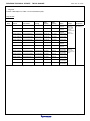
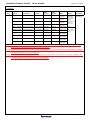
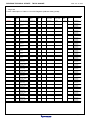
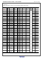
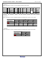
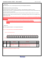
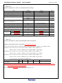
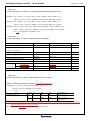
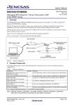
Date: Jan. 30, 2014
RENESAS TECHNICAL UPDATE
1753, Shimonumabe, Nakahara-ku, Kawasaki-shi, Kanagawa 211-8668 Japan
Renesas Electronics Corporation
Product
category
MPU/MCU
Document
No.
Corrections of
‘RX63T Group User’s Manual: Hardware Rev.2.10’
Title
TN-RX*-A086A/E
Rev.
1.00
Information
category
Technical Notification
Reference
Document
RX63T Group User’s Manual:
Hardware Rev.2.10
(R01UH0238JJ0210)
Lot No.
Applicable
Product
RX63T Group
All lots
This document describes the corrections in RX63T Group User’s Manual: Hardware Rev.2.10. Changes are
underlined in the list below.
Page 52
Correct a note to ‘Table 1.1 Outline of Specifications (7/7)’.
Note 1. Please contact Renesas Electronics sales office for derating of operation under Ta = +85°C to +105°C. Derating is the
systematic reduction of load for the sake of improved reliability.
(c) 2014. Renesas Electronics Corporation. All rights reserved.
Page 1 of 1
RENESAS TECHNICAL UPDATE TN-RX*-A086A/E
Date: Jan. 30, 2014
Page 56
Correct a description in ‘Table 1.3 List of Products (5/5)’.
Original table
Group
Part No.
Order Part No.
Package
On-chip
ROM
Capacity
On-chip
RAM
Capacity
Operating
Operating
Option
Voltage
Temperature
RX63T
R5F563TBBDFP
R5F563TBBDFP#V0
PLQP0100KB-A
256 Kbytes
24 Kbytes
CAN module
included
VCC/
PLLVCC/
VCC_USB
2.7 to 3.6V
AVCC/
AVCC0 3.0 to
3.6V or
4.0 to 5.5V
-40 to +85°C (D
Version)
R5F563TBBDFP
R5F563TBBDFP#V1
PLQP0100KB-A
256 Kbytes
24 Kbytes
CAN module
included
R5F563TEEDFB
R5F563TEEDFB#V0
PLQP0144KA-A
512 Kbytes
48 Kbytes
CAN module
not included
R5F563TEEDFA
R5F563TEEDFA#V0
PLQP0120KA-A
512 Kbytes
48 Kbytes
CAN module
not included
R5F563TEEDFH
R5F563TEEDFH#V0
PLQP0112JA-A
512 Kbytes
48 Kbytes
CAN module
not included
R5F563TEEDFP
R5F563TEEDFP#V0
PLQP0100KB-A
512 Kbytes
48 Kbytes
CAN module
not included
R5F563TCEDFB
R5F563TCEDFB#V0
PLQP0144KA-A
384 Kbytes
32 Kbytes
CAN module
not included
R5F563TCEDFA
R5F563TCEDFA#V0
PLQP0120KA-A
384 Kbytes
32 Kbytes
CAN module
not included
R5F563TCEDFH
R5F563TCEDFH#V0
PLQP0112JA-A
384 Kbytes
32 Kbytes
CAN module
not included
R5F563TCEDFP
R5F563TCEDFP#V0
PLQP0100KB-A
384 Kbytes
32 Kbytes
CAN module
not included
R5F563TBEDFB
R5F563TBEDFB#V0
PLQP0144KA-A
256 Kbytes
24 Kbytes
CAN module
not included
R5F563TBEDFA
R5F563TBEDFA#V0
PLQP0120KA-A
256 Kbytes
24 Kbytes
CAN module
not included
R5F563TBEDFH
R5F563TBEDFH#V0
PLQP0112JA-A
256 Kbytes
24 Kbytes
CAN module
not included
R5F563TBEDFP
R5F563TBEDFP#V0
PLQP0100KB-A
256 Kbytes
24 Kbytes
CAN module
not included
R5F563T6EDFM
R5F563T6EDFM#V0
PLQP0064KB-A
64 Kbytes
8 Kbytes
CAN module
not included
R5F563T5EDFM
R5F563T5EDFM#V0
PLQP0064KB-A
48 Kbytes
8 Kbytes
CAN module
not included
R5F563T4EDFM
R5F563T4EDFM#V0
PLQP0064KB-A
32 Kbytes
8 Kbytes
CAN module
not included
R5F563T6EDFL
R5F563T6EDFL#V0
PLQP0048KB-A
64 Kbytes
8 Kbytes
CAN module
not included
R5F563T5EDFL
R5F563T5EDFL#V0
PLQP0048KB-A
48 Kbytes
8 Kbytes
CAN module
not included
R5F563T4EDFL
R5F563T4EDFL#V0
PLQP0048KB-A
32 Kbytes
8 Kbytes
CAN module
not included
R5F563TEAGFB
R5F563TEAGFB#V0
PLQP0144KA-A
512 Kbytes
48 Kbytes
CAN module
included
R5F563TEAGFB
R5F563TEAGFB#V1
PLQP0144KA-A
512 Kbytes
48 Kbytes
CAN module
included
R5F563TEAGFA
R5F563TEAGFA#V0
PLQP0120KA-A
512 Kbytes
48 Kbytes
CAN module
included
R5F563TEAGFA
R5F563TEAGFA#V1
PLQP0120KA-A
512 Kbytes
48 Kbytes
CAN module
included
R5F563TEAGFH
R5F563TEAGFH#V0
PLQP0112JA-A
512 Kbytes
48 Kbytes
CAN module
included
R5F563TEAGFH
R5F563TEAGFH#V1
PLQP0112JA-A
512 Kbytes
48 Kbytes
CAN module
included
R5F563TEAGFP
R5F563TEAGFP#V0
PLQP0100KB-A
512 Kbytes
48 Kbytes
CAN module
included
R5F563TEAGFP
R5F563TEAGFP#V1
PLQP0100KB-A
512 Kbytes
48 Kbytes
CAN module
included
R5F563TCAGFB
R5F563TCAGFB#V0
PLQP0144KA-A
384 Kbytes
32 Kbytes
CAN module
included
R5F563TCAGFB
R5F563TCAGFB#V1
PLQP0144KA-A
384 Kbytes
32 Kbytes
CAN module
included
VCC/
PLLVCC
2.7 to 3.6V
AVCC0 3.0
to 3.6V
VCC/
PLLVCC
4.0 to 5.5V
VCC_USB
3.0 to 3.6V
AVCC/
AVCC0 4.0
to 5.5V
-40 to +105°C
(G Version)*1
Page 2 of 16
RENESAS TECHNICAL UPDATE TN-RX*-A086A/E
Date: Jan. 30, 2014
It should be:
Group
Part No.
Order Part No.
Package
On-chip
ROM
Capacity
On-chip
RAM
Capacity
Operating
Operating
Option
Voltage
Temperature
RX63T
R5F563TBBDFP
R5F563TBBDFP#V0
PLQP0100KB-A
256 Kbytes
24 Kbytes
CAN module
included
VCC/
PLLVCC/
VCC_USB
2.7 to 3.6V
AVCC/
AVCC0 3.0 to
3.6V or
4.0 to 5.5V
-40 to +85°C (D
Version)
R5F563TBBDFP
R5F563TBBDFP#V1
PLQP0100KB-A
256 Kbytes
24 Kbytes
CAN module
included
R5F563TEEDFB
R5F563TEEDFB#V0
PLQP0144KA-A
512 Kbytes
48 Kbytes
CAN module
not included
R5F563TEEDFA
R5F563TEEDFA#V0
PLQP0120KA-A
512 Kbytes
48 Kbytes
CAN module
not included
R5F563TEEDFH
R5F563TEEDFH#V0
PLQP0112JA-A
512 Kbytes
48 Kbytes
CAN module
not included
R5F563TEEDFP
R5F563TEEDFP#V0
PLQP0100KB-A
512 Kbytes
48 Kbytes
CAN module
not included
R5F563TCEDFB
R5F563TCEDFB#V0
PLQP0144KA-A
384 Kbytes
32 Kbytes
CAN module
not included
R5F563TCEDFA
R5F563TCEDFA#V0
PLQP0120KA-A
384 Kbytes
32 Kbytes
CAN module
not included
R5F563TCEDFH
R5F563TCEDFH#V0
PLQP0112JA-A
384 Kbytes
32 Kbytes
CAN module
not included
R5F563TCEDFP
R5F563TCEDFP#V0
PLQP0100KB-A
384 Kbytes
32 Kbytes
CAN module
not included
R5F563TBEDFB
R5F563TBEDFB#V0
PLQP0144KA-A
256 Kbytes
24 Kbytes
CAN module
not included
R5F563TBEDFA
R5F563TBEDFA#V0
PLQP0120KA-A
256 Kbytes
24 Kbytes
CAN module
not included
R5F563TBEDFH
R5F563TBEDFH#V0
PLQP0112JA-A
256 Kbytes
24 Kbytes
CAN module
not included
R5F563TBEDFP
R5F563TBEDFP#V0
PLQP0100KB-A
256 Kbytes
24 Kbytes
CAN module
not included
R5F563T6EDFM
R5F563T6EDFM#V0
PLQP0064KB-A
64 Kbytes
8 Kbytes
CAN module
not included
R5F563T5EDFM
R5F563T5EDFM#V0
PLQP0064KB-A
48 Kbytes
8 Kbytes
CAN module
not included
R5F563T4EDFM
R5F563T4EDFM#V0
PLQP0064KB-A
32 Kbytes
8 Kbytes
CAN module
not included
R5F563T6EDFL
R5F563T6EDFL#V0
PLQP0048KB-A
64 Kbytes
8 Kbytes
CAN module
not included
R5F563T5EDFL
R5F563T5EDFL#V0
PLQP0048KB-A
48 Kbytes
8 Kbytes
CAN module
not included
R5F563T4EDFL
R5F563T4EDFL#V0
PLQP0048KB-A
32 Kbytes
8 Kbytes
CAN module
not included
R5F563TEAGFB
R5F563TEAGFB#V1
PLQP0144KA-A
512 Kbytes
48 Kbytes
CAN module
included
R5F563TEAGFA
R5F563TEAGFA#V1
PLQP0120KA-A
512 Kbytes
48 Kbytes
CAN module
included
R5F563TEAGFH
R5F563TEAGFH#V1
PLQP0112JA-A
512 Kbytes
48 Kbytes
CAN module
included
R5F563TEAGFP
R5F563TEAGFP#V1
PLQP0100KB-A
512 Kbytes
48 Kbytes
CAN module
included
R5F563TCAGFB
R5F563TCAGFB#V1
PLQP0144KA-A
384 Kbytes
32 Kbytes
CAN module
included
VCC/
PLLVCC
2.7 to 3.6V
AVCC0 3.0
to 3.6V
VCC/
PLLVCC
4.0 to 5.5V
VCC_USB
3.0 to 3.6V
AVCC/
AVCC0 4.0
to 5.5V
-40 to +105°C
(G Version)*1
Page 3 of 16
RENESAS TECHNICAL UPDATE TN-RX*-A086A/E
Date: Jan. 30, 2014
Page 57
Correct a description in ‘Table 1.3 List of Products (4/5)’.
Original table
Group
Part No.
Order Part No.
Package
On-chip
ROM
Capacity
On-chip
RAM
Capacity
Operating
Operating
Option
Voltage
Temperature
RX63T
R5F563TCAGFA
R5F563TCAGFA#V0
PLQP0120KA-A
384 Kbytes
32 Kbytes
CAN module
included
VCC/
PLLVCC
4.0 to 5.5V
VCC_USB
3.0 to 3.6V
AVCC/
AVCC0 4.0 to
5.5V
-40 to +105°C
(G Version)*1
R5F563TCAGFA
R5F563TCAGFA#V1
PLQP0120KA-A
384 Kbytes
32 Kbytes
CAN module
included
R5F563TCAGFH
R5F563TCAGFH#V0
PLQP0112JA-A
384 Kbytes
32 Kbytes
CAN module
included
R5F563TCAGFH
R5F563TCAGFH#V1
PLQP0112JA-A
384 Kbytes
32 Kbytes
CAN module
included
R5F563TCAGFP
R5F563TCAGFP#V0
PLQP0100KB-A
384 Kbytes
32 Kbytes
CAN module
included
R5F563TCAGFP
R5F563TCAGFP#V1
PLQP0100KB-A
384 Kbytes
32 Kbytes
CAN module
included
R5F563TBAGFB
R5F563TBAGFB#V0
PLQP0144KA-A
256 Kbytes
24 Kbytes
CAN module
included
R5F563TBAGFB
R5F563TBAGFB#V1
PLQP0144KA-A
256 Kbytes
24 Kbytes
CAN module
included
R5F563TBAGFA
R5F563TBAGFA#V0
PLQP0120KA-A
256 Kbytes
24 Kbytes
CAN module
included
R5F563TBAGFA
R5F563TBAGFA#V1
PLQP0120KA-A
256 Kbytes
24 Kbytes
CAN module
included
R5F563TBAGFH
R5F563TBAGFH#V0
PLQP0112JA-A
256 Kbytes
24 Kbytes
CAN module
included
R5F563TBAGFH
R5F563TBAGFH#V1
PLQP0112JA-A
256 Kbytes
24 Kbytes
CAN module
included
R5F563TBAGFP
R5F563TBAGFP#V0
PLQP0100KB-A
256 Kbytes
24 Kbytes
CAN module
included
R5F563TBAGFP
R5F563TBAGFP#V1
PLQP0100KB-A
256 Kbytes
24 Kbytes
CAN module
included
R5F563TEBGFB
R5F563TEBGFB#V0
PLQP0144KA-A
512 Kbytes
48 Kbytes
CAN module
included
R5F563TEBGFB
R5F563TEBGFB#V1
PLQP0144KA-A
512 Kbytes
48 Kbytes
CAN module
included
R5F563TEBGFA
R5F563TEBGFA#V0
PLQP0120KA-A
512 Kbytes
48 Kbytes
CAN module
included
R5F563TEBGFA
R5F563TEBGFA#V1
PLQP0120KA-A
512 Kbytes
48 Kbytes
CAN module
included
R5F563TEBGFH
R5F563TEBGFH#V0
PLQP0112JA-A
512 Kbytes
48 Kbytes
CAN module
included
R5F563TEBGFH
R5F563TEBGFH#V1
PLQP0112JA-A
512 Kbytes
48 Kbytes
CAN module
included
R5F563TEBGFP
R5F563TEBGFP#V0
PLQP0100KB-A
512 Kbytes
48 Kbytes
CAN module
included
R5F563TEBGFP
R5F563TEBGFP#V1
PLQP0100KB-A
512 Kbytes
48 Kbytes
CAN module
included
R5F563TCBGFB
R5F563TCBGFB#V0
PLQP0144KA-A
384 Kbytes
32 Kbytes
CAN module
included
R5F563TCBGFB
R5F563TCBGFB#V1
PLQP0144KA-A
384 Kbytes
32 Kbytes
CAN module
included
R5F563TCBGFA
R5F563TCBGFA#V0
PLQP0120KA-A
384 Kbytes
32 Kbytes
CAN module
included
R5F563TCBGFA
R5F563TCBGFA#V1
PLQP0120KA-A
384 Kbytes
32 Kbytes
CAN module
included
R5F563TCBGFH
R5F563TCBGFH#V0
PLQP0112JA-A
384 Kbytes
32 Kbytes
CAN module
included
R5F563TCBGFH
R5F563TCBGFH#V1
PLQP0112JA-A
384 Kbytes
32 Kbytes
CAN module
included
R5F563TCBGFP
R5F563TCBGFP#V0
PLQP0100KB-A
384 Kbytes
32 Kbytes
CAN module
included
R5F563TCBGFP
R5F563TCBGFP#V1
PLQP0100KB-A
384 Kbytes
32 Kbytes
CAN module
included
VCC/
PLLVCC/
VCC_USB
2.7 to 3.6V
AVCC/
AVCC0 3.0 to
3.6V or
4.0 to 5.5V
Page 4 of 16
RENESAS TECHNICAL UPDATE TN-RX*-A086A/E
Date: Jan. 30, 2014
It should be:
Group
Part No.
Order Part No.
Package
On-chip
ROM
Capacity
On-chip
RAM
Capacity
Operating
Operating
Option
Voltage
Temperature
RX63T
R5F563TCAGFA
R5F563TCAGFA#V1
PLQP0120KA-A
384 Kbytes
32 Kbytes
CAN module
included
VCC/
PLLVCC
4.0 to 5.5V
VCC_USB
3.0 to 3.6V
AVCC/
AVCC0 4.0 to
5.5V
-40 to +105°C
(G Version)*1
R5F563TCAGFH
R5F563TCAGFH#V1
PLQP0112JA-A
384 Kbytes
32 Kbytes
CAN module
included
R5F563TCAGFP
R5F563TCAGFP#V1
PLQP0100KB-A
384 Kbytes
32 Kbytes
CAN module
included
R5F563TBAGFB
R5F563TBAGFB#V1
PLQP0144KA-A
256 Kbytes
24 Kbytes
CAN module
included
R5F563TBAGFA
R5F563TBAGFA#V1
PLQP0120KA-A
256 Kbytes
24 Kbytes
CAN module
included
R5F563TBAGFH
R5F563TBAGFH#V1
PLQP0112JA-A
256 Kbytes
24 Kbytes
CAN module
included
R5F563TBAGFP
R5F563TBAGFP#V1
PLQP0100KB-A
256 Kbytes
24 Kbytes
CAN module
included
R5F563TEBGFB
R5F563TEBGFB#V1
PLQP0144KA-A
512 Kbytes
48 Kbytes
CAN module
included
R5F563TEBGFA
R5F563TEBGFA#V1
PLQP0120KA-A
512 Kbytes
48 Kbytes
CAN module
included
R5F563TEBGFH
R5F563TEBGFH#V1
PLQP0112JA-A
512 Kbytes
48 Kbytes
CAN module
included
R5F563TEBGFP
R5F563TEBGFP#V1
PLQP0100KB-A
512 Kbytes
48 Kbytes
CAN module
included
R5F563TCBGFB
R5F563TCBGFB#V1
PLQP0144KA-A
384 Kbytes
32 Kbytes
CAN module
included
R5F563TCBGFA
R5F563TCBGFA#V1
PLQP0120KA-A
384 Kbytes
32 Kbytes
CAN module
included
R5F563TCBGFH
R5F563TCBGFH#V1
PLQP0112JA-A
384 Kbytes
32 Kbytes
CAN module
included
R5F563TCBGFP
R5F563TCBGFP#V1
PLQP0100KB-A
384 Kbytes
32 Kbytes
CAN module
included
VCC/
PLLVCC/
VCC_USB
2.7 to 3.6V
AVCC/
AVCC0 3.0 to
3.6V or
4.0 to 5.5V
Page 5 of 16
RENESAS TECHNICAL UPDATE TN-RX*-A086A/E
Date: Jan. 30, 2014
Page 58
Correct a description in ‘Table 1.3 List of Products (5/5)’.
Original table
Group
Part No.
Order Part No.
Package
On-chip
ROM
Capacity
On-chip
RAM
Capacity
Operating
Operating
Option
Voltage
Temperature
RX63T
R5F563TBBGFB
R5F563TBBGFB#V0
PLQP0144KA-A
256 Kbytes
24 Kbytes
CAN module
included
VCC/
PLLVCC/
VCC_USB
2.7 to 3.6V
AVCC/
AVCC0 3.0 to
3.6V or
4.0 to 5.5V
-40 to +105°C
(G Version)*1
R5F563TBBGFB
R5F563TBBGFB#V1
PLQP0144KA-A
256 Kbytes
24 Kbytes
CAN module
included
R5F563TBBGFA
R5F563TBBGFA#V0
PLQP0120KA-A
256 Kbytes
24 Kbytes
CAN module
included
R5F563TBBGFA
R5F563TBBGFA#V1
PLQP0120KA-A
256 Kbytes
24 Kbytes
CAN module
included
R5F563TBBGFH
R5F563TBBGFH#V0
PLQP0112JA-A
256 Kbytes
24 Kbytes
CAN module
included
R5F563TBBGFH
R5F563TBBGFH#V1
PLQP0112JA-A
256 Kbytes
24 Kbytes
CAN module
included
R5F563TBBGFP
R5F563TBBGFP#V0
PLQP0100KB-A
256 Kbytes
24 Kbytes
CAN module
included
R5F563TBBGFP
R5F563TBBGFP#V1
PLQP0100KB-A
256 Kbytes
24 Kbytes
CAN module
included
R5F563T6EGFM
R5F563T6EGFM#V0
PLQP0064KB-A
64 Kbytes
8 Kbytes
CAN module
not included
R5F563T5EGFM
R5F563T5EGFM#V0
PLQP0064KB-A
48 Kbytes
8 Kbytes
CAN module
not included
R5F563T4EGFM
R5F563T4EGFM#V0
PLQP0064KB-A
32 Kbytes
8 Kbytes
CAN module
not included
R5F563T6EGFL
R5F563T6EGFL#V0
PLQP0048KB-A
64 Kbytes
8 Kbytes
CAN module
not included
R5F563T5EGFL
R5F563T5EGFL#V0
PLQP0048KB-A
48 Kbytes
8 Kbytes
CAN module
not included
R5F563T4EGFL
R5F563T4EGFL#V0
PLQP0048KB-A
32 Kbytes
8 Kbytes
CAN module
not included
VCC/
PLLVCC
2.7 to 3.6V
AVCC0 3.0 to
3.6V
Note 1. Please contact us if you are using a G version.
Page 6 of 16
RENESAS TECHNICAL UPDATE TN-RX*-A086A/E
Date: Jan. 30, 2014
It should be:
Group
Part No.
Order Part No.
Package
On-chip
ROM
Capacity
On-chip
RAM
Capacity
Operating
Operating
Option
Voltage
Temperature
RX63T
R5F563TBBGFB
R5F563TBBGFB#V1
PLQP0144KA-A
256 Kbytes
24 Kbytes
CAN module
included
-40 to +105°C
(G Version)*1
R5F563TBBGFA
R5F563TBBGFA#V1
PLQP0120KA-A
256 Kbytes
24 Kbytes
CAN module
included
R5F563TBBGFH
R5F563TBBGFH#V1
PLQP0112JA-A
256 Kbytes
24 Kbytes
CAN module
included
R5F563TBBGFP
R5F563TBBGFP#V1
PLQP0100KB-A
256 Kbytes
24 Kbytes
CAN module
included
VCC/
PLLVCC/
VCC_USB
2.7 to 3.6V
AVCC/
AVCC0 3.0 to
3.6V or
4.0 to 5.5V
R5F563T6EGFM
R5F563T6EGFM#V0
PLQP0064KB-A
64 Kbytes
8 Kbytes
CAN module
not included
R5F563T5EGFM
R5F563T5EGFM#V0
PLQP0064KB-A
48 Kbytes
8 Kbytes
CAN module
not included
R5F563T4EGFM
R5F563T4EGFM#V0
PLQP0064KB-A
32 Kbytes
8 Kbytes
CAN module
not included
R5F563T6EGFL
R5F563T6EGFL#V0
PLQP0048KB-A
64 Kbytes
8 Kbytes
CAN module
not included
R5F563T5EGFL
R5F563T5EGFL#V0
PLQP0048KB-A
48 Kbytes
8 Kbytes
CAN module
not included
R5F563T4EGFL
R5F563T4EGFL#V0
PLQP0048KB-A
32 Kbytes
8 Kbytes
CAN module
not included
VCC/
PLLVCC
2.7 to 3.6V
AVCC0 3.0 to
3.6V
Note: Orderable part numbers are current as of when this manual was published. Please make sure to refer to the relevant
product page on the Renesas website for the latest part numbers.
Note: The products with the product ID code 1 (ex. R5F563TEADFB#V1) are the revised version to the specification constraints
of technical update TX-RX*-A84A / E described.
Note 1. Please contact Renesas Electronics sales office for derating of operation under Ta = +85°C to +105°C. Derating is the
systematic reduction of load for the sake of improved reliability.
Page 7 of 16
RENESAS TECHNICAL UPDATE TN-RX*-A086A/E
Date: Jan. 30, 2014
Page 155
Add the ADGSPMR Register to ‘Table 6.1 List of I/O Registers (Address Order) (20/56)’.
Address
000890FCh
Module
Symbol
S12AD
Register Name
A/ D Group
Scan Prior it y
Register
Symbol
ADGSPMR
Number
of bits
Access
size
16
16
Number of Access States
ICLK > PCLK
2 , 3PCLKB
ICLK < PCLK
2ICLK
Module
Name
S12ADB
Reference
Page
Remarks
Not present in
versions with
64 or 48 pins.
Con t rol
Regist er
Page 8 of 16
RENESAS TECHNICAL UPDATE TN-RX*-A086A/E
Date: Jan. 30, 2014
Page 189
Correct a description in ‘Table 6.1 List of I/O Registers (Address Order) (54/56)’.
Address
Module
Symbol
Register Name
Register
Symbol
Number
of bits
Access
size
Number of Access States
ICLK > PCLK
ICLK < PCLK
Module
Name
DPC
Reference
Page
Remarks
1633
Not present in
versions with
64 or 48 pins.
Not present in
versions with
64 or 48 pins.
Not present in
versions with
64 or 48 pins.
Not present in
versions with
64 or 48 pins.
Not present in
versions with
64 or 48 pins.
Not present in
versions with
64 or 48 pins.
Not present in
versions with
64 or 48 pins.
Not present in
versions with
64 or 48 pins.
Not present in
versions with
64 or 48 pins.
Not present in
versions with
64 or 48 pins.
Not present in
versions with
64 or 48 pins.
Not present in
versions with
64 or 48 pins.
Not present in
versions with
64 or 48 pins.
Not present in
versions with
64 or 48 pins.
Not present in
versions with
64 or 48 pins.
Not present in
versions with
64 or 48 pins.
Not present in
versions with
64 or 48 pins.
Not present in
versions with
64 or 48 pins.
Not present in
versions with
64 or 48 pins.
Not present in
versions with
64 or 48 pins.
Not present in
versions with
64 or 48 pins.
Not present in
versions with
64 or 48 pins.
Not present in
versions with
64 or 48 pins.
000C3002h
DPC
Software Start Setting
Register 0
SOFTSTAR T0
16
16
3 to 5 PCLKA
2, 3 ICLK
000C3006h
DPC
Software Start Setting
Register 1
SOFTSTAR T1
16
16
3 to 5 PCLKA
2, 3 ICLK
1633
000C300Ah
DPC
Software Start Setting
Register 2
SOFTSTAR T2
16
16
3 to 5 PCLKA
2, 3 ICLK
1633
000C300Eh
DPC
Software Start Setting
Register 3
SOFTSTAR T3
16
16
3 to 5 PCLKA
2, 3 ICLK
1633
000C3012h
DPC
Reference Value Setting VOTARGET
Register 0
0
16
16
3 to 5 PCLKA
2, 3 ICLK
1634
000C3016h
DPC
Reference Value Setting VOTARGET
Register 1
1
16
16
3 to 5 PCLKA
2, 3 ICLK
1634
000C301Ah
DPC
Reference Value Setting VOTARGET
2
Register 2
16
16
3 to 5 PCLKA
2, 3 ICLK
1634
000C301Eh
DPC
Reference Value Setting VOTARGET
Register 3
3
16
16
3 to 5 PCLKA
2, 3 ICLK
1634
000C3022h
DPC
Reference Value Select REFSEL
Register
16
16
3 to 5 PCLKA
2, 3 ICLK
1634
000C3026h
DPC
PWM Channel Setting
Register
CHLSEL
16
16
3 to 5 PCLKA
2, 3 ICLK
1635
000C302Ah
DPC
Control Enable Setting
Register
ENABLE
16
16
3 to 5 PCLKA
2, 3 ICLK
1635
000C302Eh
DPC
PARAMKP0
16
16
3 to 5 PCLKA
2, 3 ICLK
1636
000C3032h
DPC
PARAMKI0
16
16
3 to 5 PCLKA
2, 3 ICLK
1636
000C3036h
DPC
PARAMKQ0
16
16
3 to 5 PCLKA
2, 3 ICLK
1636
000C303Ah
DPC
PARAMKF0
16
16
3 to 5 PCLKA
2, 3 ICLK
1636
000C303Eh
DPC
PARAMKP1
16
16
3 to 5 PCLKA
2, 3 ICLK
1636
000C3042h
DPC
PARAMKI1
16
16
3 to 5 PCLKA
2, 3 ICLK
1636
000C3046h
DPC
PARAMKQ1
16
16
3 to 5 PCLKA
2, 3 ICLK
1636
000C304Ah
DPC
PARAMKF1
16
16
3 to 5 PCLKA
2, 3 ICLK
1636
000C304Eh
DPC
PARAMKP2
16
16
3 to 5 PCLKA
2, 3 ICLK
1636
000C3052h
DPC
PARAMKI2
16
16
3 to 5 PCLKA
2, 3 ICLK
1636
000C3056h
DPC
PARAMKQ2
16
16
3 to 5 PCLKA
2, 3 ICLK
1636
000C305Ah
DPC
Control Calculation
Parameter Setting
Register KP0
Control Calculation
Parameter Setting
Register KI0
Control Calculation
Parameter Setting
Register KQ0
Control Calculation
Parameter Setting
Register KF0
Control Calculation
Parameter Setting
Register KP1
Control Calculation
Parameter Setting
Register KI1
Control Calculation
Parameter Setting
Register KQ1
Control Calculation
Parameter Setting
Register KF1
Control Calculation
Parameter Setting
Register KP2
Control Calculation
Parameter Setting
Register KI2
Control Calculation
Parameter Setting
Register KQ2
Control Calculation
Parameter Setting
Register KF2
PARAMKF2
16
16
3 to 5 PCLKA
2, 3 ICLK
1636
Page 9 of 16
RENESAS TECHNICAL UPDATE TN-RX*-A086A/E
Date: Jan. 30, 2014
Page 190
Correct a description in ‘Table 6.1 List of I/O Registers (Address Order) (55/56)’.
Address
Module
Symbol
Register Name
Control Calculation
Parameter Setting
Register KP3
Control Calculation
Parameter Setting
Register KI3
Control Calculation
Parameter Setting
Register KQ3
Control Calculation
Parameter Setting
Register KF3
Control Calculation
Result Higher-Order
Bits Store Register 0
Control Calculation
Result Lower-Order Bits
Store Register 0
Control Calculation
Result Higher-Order
Bits Store Register 1
Control Calculation
Result Lower-Order Bits
Store Register 1
Control Calculation
Result Higher-Order
Bits Store Register 2
Control Calculation
Result Lower-Order Bits
Store Register 2
Control Calculation
Result Higher-Order
Bits Store Register 3
Control Calculation
Result Lower-Order Bits
Store Register 3
Input Code Monitor
Enable Register
Register
Symbol
Number
of bits
Access
size
PARAMKP3
16
PARAMKI3
Number of Access States
Module
Name
Reference
Page
Remarks
1636
Not present in
versions with
64 or 48 pins.
Not present in
versions with
64 or 48 pins.
Not present in
versions with
64 or 48 pins.
Not present in
versions with
64 or 48 pins.
Not present in
versions with
64 or 48 pins.
Not present in
versions with
64 or 48 pins.
Not present in
versions with
64 or 48 pins.
Not present in
versions with
64 or 48 pins.
Not present in
versions with
64 or 48 pins.
Not present in
versions with
64 or 48 pins.
Not present in
versions with
64 or 48 pins.
Not present in
versions with
64 or 48 pins.
Not present in
versions with
64 or 48 pins.
Not present in
versions with
64 or 48 pins.
Not present in
versions with
64 or 48 pins.
Not present in
versions with
64 or 48 pins.
Not present in
versions with
64 or 48 pins.
Not present in
versions with
64 or 48 pins.
Not present in
versions with
64 or 48 pins.
Not present in
versions with
64 or 48 pins.
Not present in
versions with
64 or 48 pins.
Not present in
versions with
64 or 48 pins.
ICLK > PCLK
ICLK < PCLK
16
3 to 5 PCLKA
2, 3 ICLK
16
16
3 to 5 PCLKA
2, 3 ICLK
1636
PARAMKQ3
16
16
3 to 5 PCLKA
2, 3 ICLK
1636
PARAMKF3
16
16
3 to 5 PCLKA
2, 3 ICLK
1636
RESULTU0
16
16
3 to 5 PCLKA
2, 3 ICLK
1636
RESULTL0
16
16
3 to 5 PCLKA
2, 3 ICLK
1636
RESULTU1
16
16
3 to 5 PCLKA
2, 3 ICLK
1636
RESULTL1
16
16
3 to 5 PCLKA
2, 3 ICLK
1636
RESULTU2
16
16
3 to 5 PCLKA
2, 3 ICLK
1636
RESULTL2
16
16
3 to 5 PCLKA
2, 3 ICLK
1636
RESULTU3
16
16
3 to 5 PCLKA
2, 3 ICLK
1636
RESULTL3
16
16
3 to 5 PCLKA
2, 3 ICLK
1636
TMONEN
16
16
3 to 5 PCLKA
2, 3 ICLK
1637
000C305Eh
DPC
DPC
000C3062h
DPC
000C3066h
DPC
000C306Ah
DPC
000C306Ch
DPC
000C306Eh
DPC
000C3070h
DPC
000C3072h
DPC
000C3074h
DPC
000C3076h
DPC
000C3078h
DPC
000C307Ah
DPC
000C307Eh
DPC
000C3082h
DPC
Maximum Input Code
Monitor Register 0
TMONMAX0
16
16
3 to 5 PCLKA
2, 3 ICLK
1637
000C3086h
DPC
Minimum Input Code
Monitor Register 0
TMONMIN0
16
16
3 to 5 PCLKA
2, 3 ICLK
1638
000C308Ah
DPC
Maximum Input Code
Monitor Register 1
TMONMAX1
16
16
3 to 5 PCLKA
2, 3 ICLK
1637
000C308Eh
DPC
Minimum Input Code
Monitor Register 1
TMONMIN1
16
16
3 to 5 PCLKA
2, 3 ICLK
1638
000C3092h
DPC
Maximum Input Code
Monitor Register 2
TMONMAX2
16
16
3 to 5 PCLKA
2, 3 ICLK
1637
000C3096h
DPC
Minimum Input Code
Monitor Register 2
TMONMIN2
16
16
3 to 5 PCLKA
2, 3 ICLK
1638
000C309Ah
DPC
Maximum Input Code
Monitor Register 3
TMONMAX3
16
16
3 to 5 PCLKA
2, 3 ICLK
1637
000C309Eh
DPC
Minimum Input Code
Monitor Register 3
TMONMIN3
16
16
3 to 5 PCLKA
2, 3 ICLK
1638
000C30A2h
DPC
ERRVTH0
16
16
3 to 5 PCLKA
2, 3 ICLK
1638
000C30A6h
DPC
ERRVTH1
16
16
3 to 5 PCLKA
2, 3 ICLK
1638
Not present in
versions with
64 or 48 pins.
000C30AAh
DPC
Overvoltage Output
Error Judgment
Threshold Setting
Register 0
Overvoltage Output
Error Judgment
Threshold Setting
Register 1
Overvoltage Output
Error Judgment
Threshold Setting
Register 2
ERRVTH2
16
16
3 to 5 PCLKA
2, 3 ICLK
1638
Not present in
versions with
64 or 48 pins.
Page 10 of 16
RENESAS TECHNICAL UPDATE TN-RX*-A086A/E
Date: Jan. 30, 2014
Page 191
Correct a description in ‘Table 6.1 List of I/O Registers (Address Order) (56/56)’.
Address
Module
Symbol
000C30AEh
DPC
000C30B2h
DPC
Register Name
Overvoltage Output
Error Judgment
Threshold Setting
Register 3
PWM Shut-Down at
Overvoltage Output
Error Setting Register
Register
Symbol
Number
of bits
Access
size
ERRVTH3
16
ERRDWN
16
Number of Access States
ICLK > PCLK
ICLK < PCLK
16
3 to 5 PCLKA
2, 3 ICLK
16
3 to 5 PCLKA
2, 3 ICLK
Module
Name
Reference
Page
Remarks
DPC
1638
Not present in
versions with
64 or 48 pins.
1638
Not present in
versions with
64 or 48 pins.
Page 525
Correct a description in ‘Table 21.6 Register Settings for Input/Output Pin Function in 144-Pin LQFP’.
Pin
PSEL[4:0]Settings
00000b (initial value)
P10
P11
P12
P13
P14
Hi-Z
00010b
MTCLKD
MTCLKC
—
—
—
01010b
—
—
—
CTS2# RTS2#
SS2#
SCK2
10001b
—
—
USB0_DPRPD
USB0_VBUSEN
—
Page 525
Correct a description in ‘Table 21.9 Register Settings for Input/Output Pin Function in 64-Pin LQFP’.
Pin
PSEL[3:0] Settings
0000b (initial value)
0010b
P10
P11
Hi-Z
MTCLKD
MTCLKC
Page 11 of 16
RENESAS TECHNICAL UPDATE TN-RX*-A086A/E
Date: Jan. 30, 2014
Page 525
Correct a description in ‘22.2.17 Timer Output Master Enable Register (TOER)’.
Bit
Symbol
Bit Name
Description
b0
OE3B
Master Enable MTIOC3B
0: MTU3 output is disabled *1
R/W
R/W
1: MTU3 output is enabled
b1
OE4A
Master Enable MTIOC4A
0: MTU3 output is disabled *1
R/W
1: MTU3 output is enabled
b2
OE4B
Master Enable MTIOC4B
0: MTU3 output is disabled *1
R/W
1: MTU3 output is enabled
b3
OE3D
Master Enable MTIOC3D
0: MTU3 output is disabled *1
R/W
1: MTU3 output is enabled
b4
OE4C
Master Enable MTIOC4C
0: MTU3 output is disabled *1
R/W
1: MTU3 output is enabled
b5
OE4D
Master Enable MTIOC4D
0: MTU3 output is disabled *1
R/W
1: MTU3 output is enabled
b7, b6
—
Reserved
These bits are always read as 1. The write value should be 1.
R/W
Note 1. To output a non-active level from each pin when MTU output is disabled, make necessary settings for non-active level output
from general I/O ports in the data direction registers (PDR) , port output data registers (PODR), and port mode register (PMR) in
advance. For details, refer to I/O Ports section.
Page 883
Correct a description in ‘24.2.26 General PWM Timer Cycle Setting Register (GTPR)’.
GTPR is a 16-bit readable/writable register that sets the maximum count value of GTCNT. There is one GTPR counter
for each channel.
For saw waves, the value of (GTPR + 1) is the cycle. For triangle waves, the value of (GTPR value × 2) is the cycle.
Value written to GTPR is ignored when write-protection is set to the relevant channel by the GTWP.WPn bit (n = 0 to 7).
Page 911
Correct a description in ‘24.3.2.2 Buffer Operation for GTCCRA and GTCCRB’.
(1) When GTCCRA or GTCCRB Functions as Output Compare Register
Buffer transfer is performed at an overflow (during up-count operation) or an underflow (during down-count operation)
in saw-wave mode, and at both crest and trough in triangle-wave mode.
Page 12 of 16
RENESAS TECHNICAL UPDATE TN-RX*-A086A/E
Date: Jan. 30, 2014
Page 1251
Add a chapter in ‘29.12 Usage Notes’.
35.12.14 Note in Relation to Transmit Enable Bit (TE)
When the SCR.TE bit is set to 0 (serial transmission disabled) with a pin functions as TXDn (n = 0 to 3, 12), the pin output
goes high impedance.
To avoid the TXDn line going high impedance, take any of the following methods.
(1) Connect pull-up resistor to the TXDn line.
(2) Before setting the SCR.TE bit to 0, modify the pin function to "general I/O port, output", or, after setting the
SCR.TE bit to 1, modify the pin function to TXDn.
Page 1364
Correct a description in ‘Table 31.8 Operation in CAN Reset Mode and CAN Halt Mode’.
Mode
CAN reset mode
(forcible transition)
CANM[1:0] = 11b
CAN reset mode
CANM[1:0] = 01b
CAN halt mode
Receiver
CAN module enters CAN reset
mode without waiting for the end of
message reception.
CAN module enters CAN reset
mode without waiting for the end of
message reception.
CAN module enters CAN halt mode
after waiting for the end of message
reception.*2,*3
Transmitter
CAN module enters CAN reset
mode without waiting for the end of
message transmission.
CAN module enters CAN reset
mode after waiting for the end of
message transmission.*1,*4
CAN module enters CAN halt mode
after waiting for the end of message
transmission.*1,*2,*4
Transmitter
CAN module enters CAN reset
mode without waiting for the end of
bus-off recovery.
CAN module enters CAN reset
mode without waiting for the end of
bus-off recovery.
[When the BOM[1:0] bits are 00b]
A halt request from a program will be
accepted only after bus-off recovery.
[When the BOM[1:0] bits are 01b]
CAN module automatically enters
CAN halt mode without waiting for
the end of bus-off recovery
(regardless of a halt request from a
program).
[When the BOM[1:0] bits are 10b]
CAN module automatically enters
CAN halt mode after waiting for the
end of bus-off recovery (regardless
of a halt request from a program).
[When the BOM[1:0] bits are 11b]
CAN module enters CAN halt mode
(without waiting for the end of busoff
recovery) if a halt is requested by
a program during bus-off.
CANM[1:0], BOM[1:0]: Bits in CTLR
Note 1. If several messages are requested to be transmitted, mode transition occurs after the completion of the first message
transmission. In a case that the CAN reset mode is being requested during suspend transmission, mode transition occurs when
the bus is idle, the next transmission ends, or the CAN module becomes a receiver.
Note 2. If the CAN bus is locked in dominant state, the program can detect this state by monitoring the EIFR.BLIF flag. The CAN module
does not enter CAN halt mode while the CAN bus is locked in dominant state. Enter CAN reset mode instead.
Note 3. If a CAN bus error occurs during reception after CAN halt mode is requested, the CAN module enters CAN halt mode. However,
the CAN module does not enter CAN Halt mode when the CAN bus is locked in dominant state.
Note 4. If a CAN bus error or arbitration-lost occurs during transmission after CAN reset mode or CAN halt mode is requested, the CAN
module enters the requested operating mode. However, the CAN module does not enter CAN Halt mode when the CAN bus is
locked in dominant state.
Page 13 of 16
RENESAS TECHNICAL UPDATE TN-RX*-A086A/E
Date: Jan. 30, 2014
Page 1364
Add a description in ‘34.2.12 A/D Group Scan Priority Control Register (ADGSPCR)’.
PGS Bit (Group A Priority Control Setting)
This bit sets the priority of operation on group A. Set this bit to 1 when giving priority to operation on group A.
When the PGS bit is to be set to 1, the ADCSR.ADCS[1:0] bits must be set to 01b (group scan mode). If the bits are set to any
other values, operation is not guaranteed.
When the PGS bit has been set to 0, clear operation must be performed by software according to section 34.6.2, Notes on
Stopping A/D Conversion. When the PGS bit has been set to 1, make settings according to section 34.3.4.4,Operation under
Group-A Priority Control.
When operating under group-A priority control in the group-scan mode, set to 1 to the PGSC bit of the ADGSPMR register, or
specify the frequency ratio between the peripheral module clock (PCLKB) and A/D conversion clock, ADCLK (=PCLKD) as
indicated below.
a)
PCLKB = PCLKD (Set the same value to the SCKCR. PCKB [3:0] and SCKCR. PCKD[3:0])
b)
PCLKB/2 = PCLKD (Set a value which +1 is added to the one set to the SCKCR. PCKB [3:0] to the SCKCR.
PCKD[3:0])
Page 1494
Add a new register description in ‘34.2 Register Descriptions’.
34.2.19 Group Scan Priority Control Register (ADGSPMR)
Address S12AD: ADGSPMR 0008 90FCh
b15
b14
b13
b12
b11
b10
b9
b8
b7
b6
b5
b4
b3
b2
b1
b0
PGSC
—
—
—
—
—
—
—
—
—
—
—
—
—
—
—
0
0
0
0
0
0
0
0
0
0
0
0
0
0
0
0
Value after
reset
Bit
Symbol
Bit name
Description
R/W
b14-b0
—
Reserved
These bits are read as 0. The write value should be 0.
R/W
b15
PGSC
Clock frequency setting bit
when operating under group-A
priority control
0: When operating under group-A priority control, frequency ratio
between PCLK and ADCLK is 2:1 or 1:1.
1: When operating under group-A priority control, frequency ratio
between PCLK and ADCLK is 4:1 or over.
R/W
ADGSPMR should always be accessed in 16-bits.
Page 14 of 16
RENESAS TECHNICAL UPDATE TN-RX*-A086A/E
Date: Jan. 30, 2014
Page 1743
Correct a description in ‘Table 42.1 Absolute Maximum Ratings’.
Item
Power supply voltage
USB power supply voltage
Analog power supply voltage
Reference power supply voltage
Symbol
Value
Unit
VCC, PLLVCC
–0.3 to +6.5
V
VCC_USB*1
–0.3 to +6.5
V
AVCC0, AVCC*2
–0.3 to +6.5
V
VREFH0*2
–0.3 to AVCC0 to + 0.3
V
VREF*2
–0.3 to AVCC0 to + 0.3
V
Vin
–0.3 to VCC + 0.3
V
Input voltage (USB0_DP and USB0_DM)
Vin
–0.3 to VCC_USB + 0.3
V
Input voltage (port 4)
Vin
–0.3 to AVCC0 to + 0.3
V
I nput voltage (ports 5, 6, and C)
Vin
–0.3 to AVCC to + 0.3
V
Analog input voltage (port 4)
VAN
–0.3 to AVCC0 to + 0.3
V
Analog input voltage (ports 5, 6, and C)
VAN
–0.3 to AVCC to + 0.3
V
Input voltage (except for ports 4 to 6, C,
USB0_DP, and USB0_DM)
Operating
D version product
Topr
–40 to +85
°C
temperature
G version product
Topr
–40 to +105
°C
Tstg
–55 to +125
°C
Storage temperature
Page 1747
Correct a description in ‘Table 42.6 Permissible Power Consumption’.
Table 42.6 Permissible Power Consumption (G version product only)
Note: Common standard values for conditions not given in the table are listed as “Condition 1” to “Condition 3” below.
Condition 1: VCC = PLLVCC = 2.7 to 3.6 V, VSS = PLLVSS = AVSS0 = AVSS = VREFL0 = 0 V
AVCC0 = AVCC = 3.0 to 3.6V, VREFH0 = 3.0 V to AVCC0, VREF = 3.0 V to AVCC
Condition 2: VCC = PLLVCC = 2.7 to 3.6 V, VSS = PLLVSS = AVSS0 = AVSS = VREFL0 = 0V
AVCC0 = AVCC = 4.0 to 5.5 V, VREFH0 = 4.0 V to AVCC0, VREF = 4.0 V to AVCC
Condition 3: VCC = PLLVCC = 4.0 to 5.5 V, VSS = PLLVSS = AVSS0 = AVSS = VREFL0 = 0V
AVCC0 = AVCC = 4.0 to 5.5V, VREFH0 = 4.0 V to AVCC0, VREF = 4.0 V to AVCC
Ta = -40 to +105°C. Ta is common to conditions 1 to 3.
Item
Total permissible power
consumption*1
Note.
Symbol
Typ.
Max.
Unit
Test Conditions
Pd
—
325
mW
85°C < Ta ≤ 105°C
Please contact Renesas Electronics sales office for derating of operation under Ta = +85°C to +105°C. Derating is the systematic
reduction of load for the sake of improved reliability.
Note 1. The total power consumption of the whole chip including output current.
Page 15 of 16
RENESAS TECHNICAL UPDATE TN-RX*-A086A/E
Date: Jan. 30, 2014
Page 1767
Correct a description in ‘Table 42.21 Timing of the PWM Delay Generation Circuit’.
Condition 1: VCC = PLLVCC = 2.7 to 3.6 V, VSS = PLLVSS = AVSS0 = AVSS = VREFL0 = 0 V
AVCC0 = AVCC = 3.0 to 3.6 V, VREFH0 = 3.0 V to AVCC0, VREF = 3.0 V to AVCC
Condition 2: VCC = PLLVCC = 2.7 to 3.6 V, VSS = PLLVSS = AVSS0 = AVSS = VREFL0 = 0 V
AVCC0 = AVCC = 4.0 to 5.5 V, VREFH0 = 4.0 V to AVCC0, VREF = 4.0 V to AVCC
Condition 3: VCC = PLLVCC = 4.0 to 5.5 V, VSS = PLLVSS = AVSS0 = AVSS = VREFL0 = 0 V
AVCC0 = AVCC = 4.0 to 5.5 V, VREFH0 = 4.0 V to AVCC0, VREF = 4.0 V to AVCC
Ta = Topr. Ta is common to conditions 1 to 3.
Page 1788
Correct a description in ‘Table 43.1 Absolute Maximum Ratings’.
Item
Symbol
Value
Unit
Power supply volt age
VCC
–0.3 to +4.6
V
I nput volt age ( except for por t s for 5 V
Vin
–0.3 to VCC + 0.3
V
I nput vo lt age ( port 4)
Vin
–0.3 to AVCC0 to + 0.3
V
I nput volt age ( por ts for 5 V tolera nt ) * 1
Vin
–0.3 to +5.8
V
Analog power supply volt age
AVCC0*2
–0.3 to +4.6
V
Reference power supply voltage
VREFH0*2
–0.3 to AVCC0 to + 0.3
V
Analog input volt age ( port 4)
VAN
–0.3 to AVCC0 to + 0.3
V
tolera nt* 1 and port 4)
Oper ating
D version product
Topr
–40 to +85
°C
tem pera t ure
G version product
Topr
–40 to +105
°C
Tstg
–55 to +125
°C
Sto rage te m peratu re
Page 1791
Correct a description in ‘Table 43.5 Permissible Power Consumption’.
Table 43.5 Permissible Power Consumption (G version product only)
Condition: VCC = 2.7 to 3.6 V, VSS = AVSS0 = VREFL0 = 0 V
AVCC0 = 3.0 to 3.6 V, VREFH0 = 3.0 V to AVCC0
Ta = Topr
Item
Total permissible power
consumption*1
Note.
Symbol
Typ.
Max.
Unit
Test Conditions
Pd
—
150
mW
85°C < Ta ≤ 105°C
64-pin version
Pd
—
120
mW
85°C < Ta ≤ 105 °C
48-pin version
Please contact Renesas Electronics sales office for derating of operation under Ta = +85°C to +105°C. Derating is the systematic
reduction of load for the sake of improved reliability.
Note 1. The total power consumption of the whole chip including output current.
Page 16 of 16