1
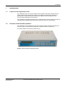
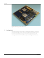
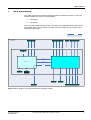
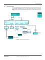
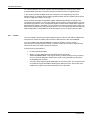
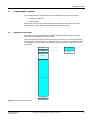
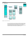
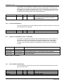
Application Note 232 Using the Cortex-M4 processor on the Microcontroller Prototyping System Document number: ARM DAI0232B Issued: May 2010 Copyright ARM Limited 2010 Application Note 232 Using the Cortex-M4 processor on the Microcontroller Prototyping System Copyright © 2010 ARM Limited. All rights reserved. Release information The following changes have been made to this Application Note. Change history Date Issue Change October 2009 A First release (Beta) May 2010 B Second release (EAC) SYS_CPUCFG register definition changed. Version controlled by Domino.Doc DS158-GENC-009974 4.0 References ii Document Issuer [1] User Manual for HMALC-AS3-52 Gleichmann Industries [2] HPE_Desk-Basic Online Help Gleichmann Industries [3] AN227 Using the Microcontroller Prototyping System with the example reference design ARM Ltd. [4] MPS QuickStart Guide ARM Ltd. [5] CH7303 HDTV / DVI Transmitter (CH7303) Data Sheet Chrontel [6] PrimeCell® Synchronous Serial Port (PL022) Technical Reference Manual ARM Ltd. [7] PrimeCell® UART (PL011) Technical Reference Manual ARM Ltd. Copyright © 2010 ARM Limited. All rights reserved. Application Note 232 ARM DAI0232B Proprietary notice ARM, ARM Powered, StrongARM, Thumb, Multi-ICE, ModelGen, PrimeCell, PrimeXsys, RealView, TrustZone, Jazelle, ARM7TDMI, ARM9TDMI, ARMulator AMBA, and The Architecture for the Digital World are registered trademarks of ARM Limited. Cortex, AXI, AHB, ARM7, ARM7TDMI-S, ARM7EJ-S, ARM720T, ARM740T, ARM9, ARM9TDMI, ARM920T, ARM922T, ARM940T, ARM9E, ARM9E-S, ARM926EJ-S, ARM946E-S, ARM966E-S, ARM968E-S, ARM996HS, ARM10, ARM1020E, ARM1022E, ARM1026EJ-S, ARM11, ARM1136J-S, ARM1136JF-S, ARM1156T2-S, ARM1156T2F-S, ARM1176JZ-S, ARM1176JZF-S, EmbeddedICE, EmbeddedICE-RT, AMBA, ARM Development Suite, ETM, ETM7, ETM9, ETM10, ETM10RV, ETM11, Embedded Trace Macrocell, Embedded Trace Buffer, ETB, ETB11, Embedded Trace Kit, Integrator, JTEK, Mali, MultiTrace, MPCore, MOVE, OptimoDE, AudioDE, SecurCore, SC100, SC110, SC200, SC210, Keil, µVision, ULINK are trademarks of ARM Limited. Java is a trademark of Sun Microsystems, Inc. XScale is a trademark of Intel Corporation. All other brand names or product names are the property of their respective holders. “ARM” is used to represent ARM Holdings plc (LSE: ARM and NASDAQ: ARMHY); its operating company ARM Limited; and the regional subsidiaries: ARM, Inc.; ARM KK; ARM Korea Ltd.; ARM Taiwan Limited; ARM France SAS; ARM Consulting (Shanghai) Co. Ltd.; ARM Belgium N.V.; AXYS Design Automation Inc.; ARM Germany GmbH; ARM Embedded Technologies Pvt. Ltd.; ARM Norway, AS; and ARMSweden AB. Neither the whole nor any part of the information contained in, or the product described in, this document may be adapted or reproduced in any material form except with the prior written permission of the copyright holder. The product described in this document is subject to continuous developments and improvements. All particulars of the product and its use contained in this document are given by ARM in good faith. All warranties implied or expressed, including but not limited to implied warranties of satisfactory quality or fitness for purpose are excluded. This document is intended only to provide information to the reader about the product. To the extent permitted by local laws ARM shall not be liable for any loss or damage arising from the use of any information in this document or any error or omission in such information. Confidentiality status This document is Open Access. This document has no restriction on distribution. Feedback on this Application Note If you have any comments on this Application Note, please send email to [email protected] giving: the document title the document number the page number(s) to which your comments refer an explanation of your comments. General suggestions for additions and improvements are also welcome. ARM web address http://www.arm.com Application Note 232 ARM DAI0232B Copyright © 2010 ARM Limited. All rights reserved. iii Table of Contents 1 INTRODUCTION .................................................................................................................. 1 1.1 Purpose of this application note.................................................................................................................................... 1 1.2 Overview of the hardware platform............................................................................................................................. 1 1.3 Getting started................................................................................................................................................................ 2 2 ABOUT THE PROCESSOR IMPLEMENTATION................................................................ 3 2.1 Fixed Configuration....................................................................................................................................................... 3 2.2 Software Programmable Configuration ...................................................................................................................... 4 3 MPS ARCHITECTURE......................................................................................................... 5 4 CPU FPGA ARCHITECTURE .............................................................................................. 6 4.1 Bus Architecture ............................................................................................................................................................ 7 4.2 Benchmarking Information .......................................................................................................................................... 8 4.3 Clocks and Resets........................................................................................................................................................... 9 5 PROGRAMMER’S MODEL................................................................................................ 11 5.1 Interrupt architecture ................................................................................................................................................. 11 5.2 Memory map ................................................................................................................................................................ 12 5.3 CPU FPGA Peripherals............................................................................................................................................... 13 5.4 CPU FPGA System Registers...................................................................................................................................... 14 5.5 DS072 I2C Interface to DVI Transmitter................................................................................................................... 18 5.6 PL022 SPI Interface..................................................................................................................................................... 19 5.7 PL011 UART Interface................................................................................................................................................ 19 6 SIGNAL ASSIGNMENTS................................................................................................... 20 6.1 Resets ............................................................................................................................................................................ 20 6.2 Clocks from Clock Factory ......................................................................................................................................... 20 6.3 Clocks to Clock Factory .............................................................................................................................................. 20 6.4 AHB-Lite Interface to DUT ........................................................................................................................................ 20 6.5 Processor Miscellaneous Signals................................................................................................................................. 20 iv Copyright © 2010 ARM Limited. All rights reserved. Application Note 232 ARM DAI0232B 6.6 Touch Screen Interface................................................................................................................................................ 21 6.7 LCD, VGA/DVI............................................................................................................................................................ 21 6.8 Human Interface (Switches and LEDs)...................................................................................................................... 21 6.9 JTAG and Trace .......................................................................................................................................................... 22 6.10 RS232 connection (X4) ................................................................................................................................................ 22 Application Note 232 ARM DAI0232B Copyright © 2010 ARM Limited. All rights reserved. v Introduction 1 Introduction 1.1 Purpose of this application note This Application Note covers the operation of the HMALC-AS3 Hpe®_module with the Hpe®_midiv2 FPGA development system from Gleichmann Electronics Research. It describes the contents of the CPU FPGA on the HMALC-AS3, including the clock structure and peripherals local to the CPU. After reading this Application Note the user should be able to use the CPU FPGA with the example reference design described in [3] or with their own DUT FPGA design. 1.2 Overview of the hardware platform This application note is designed to work on the Microcontroller Prototyping System (as shown in Figure 1) fitted with the ARM Hpe®_module (as shown in Figure 2). For further details on this system please see [1]. Figure 1: Microcontroller Prototyping System Application Note 232 ARM DAI0232B Copyright © 2010 ARM Limited. All rights reserved. 1 Introduction Figure 2: ARM Hpe®_module HMALC-AS3 1.3 Getting started The system comes pre-configured with an example design installed on the customer FPGA, described in [3]. The CPU FPGA is pre configured with the ARM Cortex-M3 processor, and BootMonitor software is loaded into the system flash memory. Refer to the MPS QuickStart Guide [4] for details of setting up and using the MPS, including how to download an alternative ARM processor image to the CPU FPGA. 2 Copyright © 2010 ARM Limited. All rights reserved. Application Note 232 ARM DAI0232B About the Processor Implementation 2 About the Processor Implementation The FPGA image supplied with this Application Note contains an implementation of the ARM Cortex-M4 (EAC release) processor, plus peripherals and bus infrastructure which are described in section 2.2. The ARM Cortex-M4 processor implements the ARMv7-M architecture. The FPGA image provided is in encrypted pof format: 2.1 fpga_processor_cm4_encrypted.pof Fixed Configuration The ARM Cortex-M4 EAC processor includes a number of configuration options that may be set when the device is synthesized. Table 1 lists the options chosen for the FPGA implementation that accompanies this Application Note. Table 2 lists the system configuration choices that are relevant to this FPGA image. The “Configuration Name” is the Verilog parameter name used to configure the processor and is included for reference for processor licencees. Core Configuration Option Configuration Name Value Comments Number of Interrupts NUM_IRQ 32 32 external IRQs Interrupt Priority LVL_WIDTH 3 8 levels of interrupt priority (2 ) Memory Protection Unit MPU_PRESENT 1 MPU present Debug Level DEBUG_LVL 3 Full debug with data matching: All debug functionality is present including data matching for watchpoint generation. 3 8 Breakpoints 4 Watchpoints Trace Level TRACE_LVL 2 Full trace: ARMv7-M ITM, ARMv7-M TPIU, ETM, and DWT triggers and counters are present. The TPIU provides 4-bit wide trace on the Mictor trace connector (“X14”). The trace clock is the same as the CPU clock. Register Reset RESET_ALL_REGS 0 Only essential registers are reset Debug Interface JTAG_PRESENT 1 JTAG and Serial Wire debug interfaces supported by the DAP Architectural Clock Gating CLKGATE_PRESENT 0 Clock gating is not implemented in the FPGA Wake-up Interrupt Controller WIC_PRESENT 0 The WIC is not implemented in the FPGA Bit band support BB_PRESENT 1 Bit banding is implemented in the FPGA FPU support FPU_PRESENT 1 FPU is implemented in the FPGA Table 1: Cortex-M4 Processor Configuration Application Note 232 ARM DAI0232B Copyright © 2010 ARM Limited. All rights reserved. 3 About the Processor Implementation System Configuration Option Comments Power Management Unit Sleep modes will not offer any power saving because there is no PMU implemented in the FPGA. System Timer Reference Clock The SysTick timer is provided with a 100kHz reference clock. Multi Processor Communications The processor TXEV and RXEV pins are exported to the DUT. FPU exception event The processor FPIXC, FPOFC, FPUFC, FPIOC, FPDZC and FPIDC pins are not used. The appropriate 10ms calibration value is also provided. Table 2: Cortex-M4 System Configuration 2.2 Software Programmable Configuration Some aspects of the processor and system may be dynamically configured by software using the CPU FPGA System Registers (see section 5.4). Table 3 shows the software configurable features in this FPGA image. Configuration Register Comments SYS_CPUCFG The Cortex-M4 MPUDISABLE, FPUDISABLE and DBGEN signals are driven by SYS_CPUCFG register. SYS_BASE The Cortex-M4 FPGA does not support any software programmable configuration. The SYS_BASE register is Read-Only. The SYS_BASE reflect the location of the CoreSight debug ROM table. Table 3: Software Programmable Configuration The SYS_CPUCFG register is readable and writable. The definition of the SYS_CPUCFG register (0xDFFF0028) is shown in Table 4. Bit Definition Reset Connected signals Valid values 31:3 Reserved - - Read as 0 2 Debug Disable 0 Invert of DBGEN 0 – Debug enabled, 1 – Debug disabled 1 FPU Disable 0 FPU_DISABLE 0 – FPU functional, 1 – FPU disabled 0 MPU Disable 0 MPU_DISABLE 0 – MPU functional, 1 – MPU disabled Table 4: SYS_CPUCFG register definition. 4 Copyright © 2010 ARM Limited. All rights reserved. Application Note 232 ARM DAI0232B MPS Architecture 3 MPS Architecture The Gleichmann Microcontroller Prototyping System includes two FPGAs on which an AHB-Lite (AMBA 2.0) system is implemented: CPU FPGA DUT FPGA Figure 3 shows a high-level block view of the MPS. This Application Note describes the CPU FPGA. Refer to [3] for details of the DUT FPGA, including how to customize and rebuild the DUT FPGA. Implemented Not Implemented Hpe®_midiv2 Base Board I/O I/O UART Switches LEDs HMALC-AS3 Processor Board Switches LEDs Ethernet 7SEG Char LCD Ethernet I/O CAN Flexray LIN Trace/JTAG Trace Debug Interrupts CPU FPGA AHB Lite DUT FPGA Video SMB SMB SSRAM SSRAM NOR Video DMB SMB DDR USB Video I/F UARTS AC97 SD/MMC I2C SPI I/O Figure 3: Block diagram of the Microcontroller Prototyping System Application Note 232 ARM DAI0232B Copyright © 2010 ARM Limited. All rights reserved. 5 CPU FPGA Architecture 4 CPU FPGA Architecture The CPU FPGA contains: ARM Cortex-M4 processor with o Serial Wire and JTAG Debug Access Port (DAP) o ARMv7-M Embedded Trace Macrocell (ETM) o ARMv7-M Instrumentation Trace Macrocell (ITM) o ARMv7-M Trace Port Interface Unit (TPIU) AHB Memory Controllers that interface to o 64k FPGA RAM (Internal “No Bus Latency” RAM) o 8MB SSRAM (Zero Bus Turnaround SSRAM) o 64MB NOR FLASH AHB Master Interface to the DUT FPGA AHB to APB bridge o o o APB Registers Configuration of local components Interfaces to LEDs and Switches APB PrimeCell Components PL011 UART (UART 3) PL022 SSP (interface to TouchScreen controller) APB Components Application Note 232 ARM DAI0232B 2 DS702 I C (interface to DVI Transmitter) Copyright © 2010 ARM Limited. All rights reserved. 6 CPU FPGA Architecture 4.1 Bus Architecture The CPU FPGA implements an AHB bus infrastructure to give the processor access to the local FLASH and SSRAM memory, and to the Customer DUT FPGA. An APB bus is used to connect local PrimeCell APB peripherals. Figure 4 shows the full AHB and APB system. External Device 0xE000_0000 0xE00F_FFFF Cortex-M4 0x0000_0000 0x1FFF_FFFF I 0x2000_0000 0xDFFF_FFFF 0xE010_0000 0xFFFF_FFFF Private Peripheral Bus DUT FPGA D CPU FPGA S code mux AHB Lite mux 0x0000_0000 0x03FF_FFFF 0x1000_0000 0x103F_FFFF 0x1800_0000 0x1BFF_FFFF AHB Lite mux 0x1EFF_0000 0x1EFF_FFFF 0x2000_0000 0x203F_FFFF RAM FPGA SMC0 0x3000_0000 0xDFFD_FFFF 0xE010_0000 0xFFFF_FFFF 0xDFFF_0000 0xDFFF_FFFF AHB to APB SMC1 APB Config registers I/O PADS I/O PADS I/O PADS I/O PADS PL011 (3) PL022 (0) DS702 (0) DUT FPGA CS0 SSRAM0 CS1 SSRAM1 CS0 FLASH AHB Interface to DUT FPGA 0x2000_0000 0x203F_FFFF 0x1000_0000 And remaped to 0x103F_FFFF 0x0000_0000 0x0000_0000 And aliased to 0x03FF_FFFF 0x1800_0000 Figure 4: CPU FPGA Bus Architecture Application Note 232 ARM DAI0232B Copyright © 2010 ARM Limited. All rights reserved. 7 CPU FPGA Architecture 4.2 Benchmarking Information Table 5 describes the cycle performance of the CPU FPGA components shown in Figure 4. This information should be considered when benchmarking the performance of software running on the MPS. Component Wait States Note AHB-Lite Mux 0 Implemented as combinatorial logic, and therefore do not introduce any cycle delays even when switching between segments. SSRAM0 0 The two SSRAM blocks use ZBT RAMs to provide zero wait state access. SSRAM1 0 (best case) SSRAM1 shares physical pins with FLASH, so wait states may be incurred when accessing the FLASH and SSRAM1 in sequence. For benchmarking purposes, it is advisable to avoid using both the FLASH and SSRAM1 simultaneously. For best performance, program code from FLASH can be copied to SSRAM1 for execution. FLASH 3 (default) The FLASH memory interface inserts wait states according to the value programmed in SYS_WSCFG and the clock frequency selected by SYS_CLKCFG, see section 5.4 for further details. RAM FPGA 0 The RAM FPGA block uses FPGA “No Bus Latency RAM” internally to provide zero wait state access. AHB to APB Bridge 1 The AHB-APB bridge adds 1 wait state for accesses to the local peripherals and System Registers. Table 5: AHB Component Cycle Performance Application Note 232 ARM DAI0232B Copyright © 2010 ARM Limited. All rights reserved. 8 CPU FPGA Architecture 4.3 Clocks and Resets The example reference system application note [3] details the clock and reset structure of the overall MPS system. Figure 5 shows the clocks used within the CPU FPGA. CLK100M CPU_PLL_ L2_CLKOUT0 (25M) CPU_PLL_ R2_CLKOUT0 (1M-50M) CLK10p (25M) CLK1p CPU FPGA HCLK (CPU + AHB) PLL PL011 UART Reference Clock Selector PL022 SPI Reference Clock ÷ SYS_CLKCFG CPU SysTick Reference Clock Figure 5: CPU FPGA Clocks The CPU FPGA uses the following clocks: CLK100M: 100MHz reference from the oscillator (to drive the PLL) CLK1p: HCLK from the clock factory (AHB subsystem) CLK10p: 25MHz reference from the clock factory (PrimeCell reference clock for SPI and UART, and divided down to generate 100kHz SysTick external clock reference) The CPU FPGA generates the following clocks: CPU_PLL_R2_CLKOUT0: for use as HCLK when re-distributed by the Clock Factory CPU_PLL_L2_CLKOUT0: 25MHz clock to Clock Factory The CPU FPGA uses one internal PLL to generate a range of fixed clock frequencies from the 100MHz reference clock. A software controllable block allows code running on the processor, or a debugger, to change the HCLK frequency of the system by switching between these PLL generated clocks. See section 5.4.7 for details of how to program the HCLK frequency. Application Note 232 ARM DAI0232B Copyright © 2010 ARM Limited. All rights reserved. 9 CPU FPGA Architecture For normal operation, the Clock Factory must be configured to route the CPU FPGA programmable clock back to the CPU and DUT FPGAs as HCLK on signal CLK1p. If you need to operate the MPS at an HCLK frequency not supported by the clock switcher above, a suitable HCLK must be generated within the DUT FPGA and the Clock Factory configured to route it to CLK1p. Since the flash wait state configuration register adjusts automatically according to the clock frequency selection, in such case (using DUT for system clock generation), you may still want to program the clock configuration register and the flash configuration register to adjust the flash memory wait state. At reset (power-on-reset as well as system reset), the flash memory defaults to 3 wait states per access. You must ensure that the selected wait state configuration is acceptable for the HCLK frequency you are driving from the DUT. 4.3.1 Resets The CPU FPGA is reset by the USER_RESET# signal. The PLL lock status output is also factored in to ensure the FPGA does not leave reset before the PLL has stabilized. The CPU FPGA drives the AHB HRESETn signal to the DUT FPGA to create a synchronous reset with respect to HCLK. The DUT FPGA can use this to resynchronise resets to all other local clock domains as required. A Reset may be generated by: 10 Pushing the Reset Button Writing 1 to the ARM Cortex-M architected reset request bit, AIRCR.SYSRESETREQ. This may be done by code executing on the processor or by an external debugger. Note that the reset is not guaranteed to take place immediately after the write. The DUT FPGA asserts signal WDOGRES to the CPU FPGA. This could be used to implement a programmable watchdog timer within the DUT. See section 6 for details of the signal connections between the CPU and DUT. Copyright © 2010 ARM Limited. All rights reserved. Application Note 232 ARM DAI0232B Programmer’s model 5 Programmer’s model This chapter describes the MPS Programmer’s Model in terms of the CPU FPGA: Interrupt Architecture Memory Map Parts of the memory map and interrupt allocation depend on the system in the DUT FPGA. Refer to [3] for details of the example DUT reference design. 5.1 Interrupt architecture The ARM Cortex-M processor family include a Nested Vectored Interrupt Controller (NVIC) which is integrated into the processor. Figure 6 shows the mapping of external interrupts to the NVIC. The top eight interrupts are reserved for use within the CPU FPGA as shown. The remaining interrupts and NMI are available to the DUT FPGA. The allocation of these interrupts is dependent on the DUT FPGA. [31] PL022 [30] PL011 (0) UART (3) [29] Reserved (Ext touchscreen) [28] Reserved (CPU FPGA CLCD) SPI touchscreen DUT FPGA CPU FPGA [27] [26] Reserved [25] [24] [23] [22] [21] [20] [19] [18] [17] [16] [15] [14] [13] [12] From DUT FPGA [11] [10] [09] [08] [07] [06] [05] [04] [03] [02] [01] [00] NMI From DUT FPGA Figure 6: Interrupt Allocation Table Application Note 232 ARM DAI0232B Copyright © 2010 ARM Limited. All rights reserved. 11 Programmer’s model 5.2 Memory map External Device 0x10000_0000 Private Peripheral Bus 0xE000_0000 System Bus 0xF000_0000 0xE010_0000 V6-M V7-M 0xE000_0000 Processor PPB 0xD000_0000 Ext Periph non Exec V6-M: Reserved V7-M: System Bus Reserved ˜ DUT FPGA ˜ 0xDFFF_6000 0xDFFF_0FFC 0xDFFF_0000 Config Regs 0xDFFF_5000 PL011 (3) 0xDFFE_0000 Reserved 0xDFFF_4000 PL022 (TouchScrn) ˜ ˜ ˜ 0xDFFF_2000 Reserved 0xDFFF_003C ID2 0xDFFF_1000 Reserved 0xDFFF_0038 Debug BASE 0xDFFF_0000 CPU Sys Regs 0xDFFF_0034 Reserved 0xDFFF_0030 Reserved Ext Periph non Exec 0xA000_0000 0x2FFF_FFFF Ext RAM Exec 0x9000_0000 CPU Config 0xDFFF_0024 Wait State Config 0x2000_0000 SSRAM0 (4M) SSRAM0 (4M) 0xDFFF_0020 Clock Config 0x1F00_0000 Reserved Reserved 0xDFFF_001C Reserved 0x1EFF_0000 RAM FPGA (64k) RAM FPGA (64k) 0xDFFF_0018 Reserved 0xDFFF_0014 Misc CTRL1 Ext RAM Exec 0x7000_0000 ˜ Reserved ˜ 0x1C00_0000 Ext RAM Exec ˜ ˜ Reserved 0x6000_0000 ˜ Periph non Exec Flash (64M alias) ˜ 0x1800_0000 ˜ Periph non Exec 0x4000_0000 Reserved 0xDFFF_0028 Reserved 0x2040_0000 0x5000_0000 0xDFFF_002C Reserved Ext RAM Exec 0x8000_0000 ˜ DS702 (I2C DVI) Ext Periph non Exec 0xB000_0000 CPU FPGA Reserved 0xDFFF_3000 Ext Periph non Exec 0xC000_0000 0xDFFF_1000 0x1080_0000 Reserved ˜ ˜ Reserved ˜ 0xDFFF_0010 TS Status 0xDFFF_000C CPU LEDs 0xDFFF_0008 CPU Switches 0xDFFF_0004 Remap/Alias 0xDFFF_0000 System ID 0x1040_0000 Int RAM Exec 0x3000_0000 0x1000_0000 SSRAM1 (4M) SSRAM1 (4M) ALIAS = 1 ALIAS = 0 Int RAM Exec 0x2000_0000 0x1000_0000 Int ROM Exec 0x1000_0000 ˜ Int ROM Exec Reserved ˜ ˜ Reserved ˜ 0x0000_0000 0x0400_0000 Flash (60M) 0x0040_0000 0x0000_0000 Flash (64M) SSRAM1 (4M) REMAP = 1 REMAP = 0 Figure 7: CPU FPGA memory map Figure 7 shows the memory map of the CPU FPGA. SSRAM0 provides 4MB of RAM in the architected (ARMv6-M and ARMv7-M) SRAM memory region. SSRAM1 provides an additional 4MB of RAM within the architected CODE memory region. SSRAM1 can be used to provide zero wait state code access in fast systems, and to allow code development without the need to reprogram the Flash memory. The REMAP and ALIAS control bits are available to software via the SYS_MEMCFG register. 12 Copyright © 2010 ARM Limited. All rights reserved. Application Note 232 ARM DAI0232B Programmer’s model 5.3 CPU FPGA Peripherals The CPU FPGA includes the local peripherals listed in Table 6. Details of the PrimeCell UART (PL011) and SSP (PL022) can be found in [7] and [6]. Details of the DS072 and the CPU System Registers can be found in section 5.4. Address Peripheral Usage 0xDFFF6000 – 0xDFFFFFFF Reserved 0xDFFF5000 – 0xDFFF5FFF PL011 RS232 interface UART3, used by BootMonitor 0xDFFF4000 – 0xDFFF4FFF PL022 SSP interface to touchscreen controller on Hpe_midiv2 0xDFFF3000 – 0xDFFF3FFF DS072 I C interface to DVI Transmitter on Hpe_midiv2 0xDFFF1000 – 0xDFFF2FFF Reserved 0xDFFF0000 – 0xDFFF0FFF CPU System Registers 2 LEDs, Switches and local configuration controls Table 6: CPU FPGA Peripherals Application Note 232 ARM DAI0232B Copyright © 2010 ARM Limited. All rights reserved. 13 Programmer’s model 5.4 CPU FPGA System Registers The CPU System Registers are based at address 0xDFFF0000. Table 7 lists the registers. Full descriptions can be found in the following sections. Address Register Description 0xDFFF0000 SYS_ID ID Registers 0xDFFF0004 SYS_MEMCFG Memory Configuration (including REMAP and ALIAS controls) 0xDFFF0008 SYS_SW CPU DIP Switches 0xDFFF000C SYS_LED CPU LEDs 0xDFFF0010 SYS_TS TouchScreen Status 0xDFFF0014 SYS_CTRL1 Miscellaneous Configuration 0xDFFF0018 Reserved 0xDFFF001C Reserved 0xDFFF0020 SYS_CLKCFG Clock Configuration 0xDFFF0024 SYS_WSCFG Wait State Configuration 0xDFFF0028 SYS_CPUCFG CPU Configuration 0xDFFF002C Reserved 0xDFFF0030 Reserved 0xDFFF0034 Reserved 0xDFFF0038 SYS_BASE Debug Access Port CoreSight Component Pointer Address 0xDFFF003C SYS_ID2 Secondary Identification Register 0xDFFF0040 – 0xDFFF0FFC Reserved Table 7: CPU FPGA System Registers 5.4.1 SYS_ID (0xDFFF0000) The System Identification register returns a value specific to the CPU FPGA image. Name REV BOARD VARIANT ARCH BUILD Application Note 232 ARM DAI0232B Bits 31:28 27:16 15:12 11:8 7:0 Access RO RO RO RO RO Reset ‘h1 ‘h023 ‘h0 ‘h4 ‘hxx Note Board Revision B HBI Board number Build Variant of board Bus Architecture (4 AHB, 5 AXI) FPGA build Copyright © 2010 ARM Limited. All rights reserved. 14 Programmer’s model 5.4.2 SYS_MEMCFG (0xDFFF0004) The Memory Configuration register is reset only by power-on-reset – soft resets such as debug or system reset do not alter the state of this register. The default value allows the MPS to boot from Flash memory. Refer to section 5.1 for details of the function of the REMAP and ALIAS bits. Name Bits Reserved ALIAS REMAP 31:2 1 0 5.4.3 Access Power On Reset Note RW RW Alias FLASH. 1 is Aliased on 0 Aliased off Remap SSRAM. 1 is Remap on 0 Remap off ‘b1 ‘b0 SYS_SW (0xDFFF0008) The Switch register returns the value of the eight switches (arranged as two groups of four) labeled “P1” and “P2” on the HMALC-AS3 board [1]. Name Reserved USER_SWITCH 5.4.4 Bits 31:8 7:0 Access Reset Note RO Value depends on switch settings ‘h-- SYS_LED (0xDFFF000C) The LED register controls the eight processor LEDs on the HMALC-AS3 board [1], unless overridden by SYS_CTRL1. Name Reserved LED 5.4.5 Bits 31:8 7:0 Access Reset Note RW Write 1 to light the corresponding LED. Reads return the last value written to the register. ‘h00 SYS_TS (0xDFFF0010) The TouchScreen status register shows the busy and interrupt status from a touchscreen device on the Hpe_midiv2 baseboard. Name Reserved TS_INT TS_BUSY Application Note 232 ARM DAI0232B Bits 31:2 1 0 Access Reset Note RO RO External Interrupt from Touchscreen External Busy signal from Touchscreen ‘b‘b- Copyright © 2010 ARM Limited. All rights reserved. 15 Programmer’s model 5.4.6 SYS_CTRL1 (0xDFFF0014) The Miscellaneous control register allows the function of the eight processor LEDs that are normally controlled by the SYS_LED register to be overridden with the status of various processor outputs. The output signals are pulse-stretched to ensure that singlecycle pulses are visible as flashes on the LEDs. Name Reserved LED_FUNC 5.4.7 Bits 31:1 0 Access Reset Note RW Write 0 to drive LEDs from SYS_LED register. Write 1 to drive LEDs from CPU status signals: 7: SLEEPING 6: SLEEPDEEP 5: HALTED 4: LOCKUP 3: SYSRESETREQ 2: TXEV 1: WAKEUP 0: DBGRESTARTED ‘b0 SYS_CLKCFG (0xDFFF0020) The Clock Configuration register allows the clock speed of the processor and its AHB subsystem to be modified easily by software for benchmarking purposes. Attempting to write a reserved value to this register will result in a valid clock value being selected. Note that when 12MHz setting is used, the duty cycle of the output clock can either be 40% or 60%. Name Reserved CLOCKCFG 16 Bits 31:4 3:0 Access Reset Note RW 0xF, 0xE – Reserved 0xD – 50MHz 0xC – 40MHz 0xB – 30MHz 0xA – 25MHz 0x9 – 20MHz 0x8 – 15MHz 0x7 – 12MHz 0x6 – 10MHz 0x5 – 8MHz 0x4 – 6MHz 0x3 – 4MHz 0x2 – 2MHz 0x1 – 1MHz 0x0 – Reserved ‘hD Copyright © 2010 ARM Limited. All rights reserved. Application Note 232 ARM DAI0232B Programmer’s model 5.4.8 SYS_WSCFG (0xDFFF0024) The Wait State configuration register controls the number of wait-states inserted by the memory controller when accessing Flash memory. The default value of three wait states is required for the default operating frequency of 50MHz. The register contains hardware logic to determine if the write data is valid for the current operating frequency and automatically forces the write data to a valid value if necessary. If the clock frequency setting is updated to a higher frequency, WSCFG is automatically updated to a valid value if necessary. Table 8 shows the valid wait state configurations when running at the different clock frequencies supported by SYS_CLKCFG. Name Reserved WSCFG Frequency (MHz) 40, 50 30 15, 20, 25 1, 2, 4, 6, 8, 10, 12 Bits 31:2 1:0 Access Reset Note RW 0x3 – 3 wait states on read, 3 wait states on write 0x2 – 2 wait states on read, 2 wait states on write 0x1 – 1 wait state on read, 1 wait state on write 0x0 – 0 wait state on read, 1 wait state on write 3 Wait States Yes Yes Yes Yes ‘h3 2 Wait States Yes Yes Yes 1 Wait State Yes Yes 0 Wait State Yes Table 8: Valid Wait State Configurations 5.4.9 SYS_CPUCFG (0xDFFF0028) The CPU Configuration register is used to control various processor specific features. Refer to section 2 to determine if and how this register is used by the processor FPGA. Name Bits 31:8 Access Reset --- Note Processor Specific – Refer to section 2 5.4.10 SYS_BASE (0xDFFF0038) The SYS_BASE register drives the value that an external (Serial Wire or JTAG) debugger sees when connecting to the Debug Access Port and reading its BASE register. Refer to section 2 to determine if this feature is supported by the processor FPGA. BASEADDRESS is reset by power-on-reset to the ARMv6-M and ARMv7-M architected value for the processor ROM table. Soft resets such as debug or system reset do not alter the state of this register. Application Note 232 ARM DAI0232B Copyright © 2010 ARM Limited. All rights reserved. 17 Programmer’s model This register may be updated by software to point to a system level ROM table in the DUT FPGA, which in turn points to the architected processor ROM table. The system level ROM table(s) may provide identification of the user’s customized processor system and any additional CoreSight compliant peripherals within it. This register allows the user to test debug tools connectivity with such customized systems. Name BASEADDRESS Bits 31:0 Access Reset Note See ‘hE00FF003 This register will be RO if the processor FPGA Note does not support reprogramming of the DAP BASE register value. 5.4.11 SYS_ID2 (0xDFFF003C) The SYS_ID2 register may contain additional CPU FPGA build information. The format of that information is not specified. Name ID_2 5.5 Bits 31:0 Access Reset RO ‘hx Note Reserved for ARM internal use. DS072 I2C Interface to DVI Transmitter 2 The DS072 I C peripheral is based at address 0xDFFF3000 and is used to interface to the DVI transmitter [5] on the baseboard. The DS072 implements a simple register 2 interface only – the I C protocol must be generated in software using a “bit-banging” technique. Table 9 lists the registers. Full descriptions can be found in the following sections. Address Register Description 0xDFFF3000 SB_CONTROL Status Register 0xDFFF3000 SB_CONTROLS Output Set Register (Note – Same address as SB_CONTROL) 0xDFFF3004 SB_CONTROLC Output Clear Register 2 Table 9: DS072 I C Registers 5.5.1 SB_CONTROL (0xDFFF3000) The SB_CONTROL register returns the value of the serial data (SDA) and serial clock (SCL) pins when read. Name Reserved SB_SDA SB_SCL 18 Bits 31:2 1 0 Access Reset Note RO RO Level of SDA signal Level of SCL signal ‘b0 ‘b0 Copyright © 2010 ARM Limited. All rights reserved. Application Note 232 ARM DAI0232B Programmer’s model 5.5.2 SB_CONTROLS (0xDFFF3000) The SB_CONTROLS (SET) register allows the SDA and SCL pins to be pulled high by pullup resistors on the board by writing ‘b1 to the corresponding bit. Name Reserved SB_nSDAOUTEN SB_SCLOUT 5.5.3 Bits 31:2 1 0 Access Reset Note W W Sets SDA line when 1 Sets SCL line when 1 ‘b0 ‘b0 SB_CONTROLC (0xDFFF3004) The SB_CONTROLC (CLEAR) register allows the SDA and SCL pins to be driven low by writing ‘b1 to the corresponding bit. Name Reserved SB_nSDAOUTEN SB_SCLOUT 5.6 Bits 31:2 1 0 Access Reset Note W W Clears SDA line when 1 Clears SCL line when 1 ‘b0 ‘b0 PL022 SPI Interface The PL022 PrimeCell peripheral is based at address 0xDFFF4000 and is used to interface to the touchscreen on the baseboard. 5.7 PL011 UART Interface The PL011 PrimeCell peripheral is based at address 0xDFFF5000 and provides the UART3 RS-232 serial interface. This interface may be used by the BootMonitor software, see [3] for more details. Application Note 232 ARM DAI0232B Copyright © 2010 ARM Limited. All rights reserved. 19 Signal assignments 6 Signal assignments 6.1 Resets FPGA Signal USER_RESETn 6.2 Direction [Width] input Clocks from Clock Factory FPGA Signal CPU_CLK1 CPU_CLK5 CPU_CLK10 CPU_CLK15 CPU_CLK100M 6.3 Direction [Width] input input input input input Note AHB and Processor clock input, HCLK. Not used. Peripheral reference clock input, 25MHz. Not used. 100MHz reference clock. Clocks to Clock Factory FPGA Signal CPU_PLL_L2_CLKOUT0 CPU_PLL_R2_CLKOUT0 CPU_PLL_B1_CLKOUT3 CPU_PLL_T1_CLKOUT3 6.4 Note User reset Direction [Width] output output output output Note Peripheral reference clock from FPGA PLL. 25MHz AHB and Processor clock from FPGA PLL. 1-50MHz Not used by clock factory. 60MHz. Not used by clock factory. 40MHz. AHB-Lite Interface to DUT The CPU FPGA implements a 32bit AHB-Lite master interface to the DUT FPGA. FPGA Signal FPGA_IC[31:0] FPGA_IC[32] FPGA_IC[35:33] FPGA_IC[36] FPGA_IC[40:37] FPGA_IC[43:41] FPGA_IC[45:44] FPGA_IC[46] FPGA_IC[78:47] FPGA_IC[110:79] FPGA_IC[111] FPGA_IC[112] FPGA_IC[113] 6.5 Direction [Width] output [31:0] output output output output [3:0] output [2:0] output [1:0] output output [31:0] input [31:0] input input output Note HWDATA HWRITE HBURST[2:0] HMASTLOCK HPROT HSIZE HTRANS Reserved for HSEL, tied to 1’b1 HADDR HRDATA HRESP HREADY HRESETn Processor Miscellaneous Signals The following CPU signals are exported to the DUT FPGA. FPGA Signal FPGA_IC[125:114] L14_DUTOUT_DN[11:0] L14_DUTOUT_DN[12] L14_CPUOUT_DN[0] L14_CPUOUT_DN[1] L14_CPUOUT_DN[2] 20 Direction [Width] input [11:0] input [23:12] input output output output Note INT[11:0] INT[23:12] NMI SLEEPING SLEEPDEEP HALTED Copyright © 2010 ARM Limited. All rights reserved. Application Note 232 ARM DAI0232B Signal assignments L14_CPUOUT_DN[3] L14_CPUOUT_DN[4] L14_CPUOUT_DN[5] L14_CPUOUT_DN[6] output output input input L14_CPUOUT_DN[12:7] L14_CPUOUT_DP[9:0] L14_CPUOUT_CLK N/C N/C N/C 6.6 LOCKUP TXEV RXEV - Tie low if not used by DUT. WDOGRES – Watchdog Reset Request, tie low if not used by DUT. Touch Screen Interface The TouchScreen SPI interface is driven by PrimeCell PL022 [6]. Additional signals are visible via the TouchScreen Status Register, see section 5.4.5. FPGA Signal TOUCH_SPI_BUSY TOUCH_SPI_CS# TOUCH_SPI_DCLK TOUCH_SPI_DIN TOUCH_SPI_DOUT TOUCH_SPI_IRQ# 6.7 Direction [Width] input output output input output input Note Connects to TS_BUSY Driven by TS_FSSOUT Driven by TS_CLK Connects to TS_DIN Driven by TS_DOUT Connects to TS_INTn LCD, VGA/DVI The CPU FPGA de-multiplexes signals from the DUT FPGA and passes them on to the LCD connector and DVI transmitter. Refer to [3] for details of how to drive these interfaces from the DUT FPGA. 2 The DVI Transmitter [5] is controlled using an I C interface as described in section 5.5. Figure 8 shows the electrical connections for this interface. 2 Figure 8: Video I C Connections 6.8 Human Interface (Switches and LEDs) FPGA Signal CPU_DSW CPU_LED Application Note 232 ARM DAI0232B Direction [Width] input [7:0] output [7:0] Note Read via System register SYS_SW. Set via System Register SYS_LED. Copyright © 2010 ARM Limited. All rights reserved. 21 Signal assignments 6.9 JTAG and Trace The Processor FPGA can support JTAG / Serial Wire debug interfaces and a Trace interface. Refer to section 2 to determine the options supported by the processor. The JTAG/Serial Wire debug interface is available on two connectors; the rear-panel debug connector and the internal Mictor connector. The debug interface signals are routed to the rear-panel connector if a debugger cable is detected, otherwise they are routed to the Mictor connector. 6.9.1 Rear-Panel JTAG Connector (X14 - “Debug”) FPGA Signal Direction [Width] Note FTSH_GNDDET bi-dir Connector Detect. Weak pull-up on FPGA which is pulled low by the connector to indicate a connection. FTSH_TMS bi-dir Input to SWDIOTMS on processor. Also used as Data Out for Serial Wire Debug. FTSH_TCK bi-dir JTAG Clock to processor. FTSH_TDO bi-dir JTAG Data Out from processor. FTSH_TDI bi-dir JTAG Data In to processor. FTSH_TRST bi-dir JTAG Reset. This is an active low signal. 6.9.2 Mictor Connector (X14) The Mictor connector allows a Trace probe to be connected to processors that support ETM. FPGA Signal INTCPU_TDI INTCPU_TDO INTCPU_TCK INTCPU_TMS Direction [Width] input bi-dir input input INTCPU_TRSTn INTCPU_SRSTn INTCPU_RTCK INTCPU_DBGRQ INTCPU_DBGACK MICTOR_PIPESTAT0 MICTOR_PIPESTAT1 MICTOR_PIPESTAT2 MICTOR_EXTTRIG MICTOR_TRACEPKT MICTOR_TRACESYNC MICTOR_TRACECLK input input output input output output output output output output[15:0] output output 6.10 Note JTAG Data In to processor. JTAG Data Out from processor. JTAG Clock to processor. Input to TMS on processor. This is not connected to the Serial Wire Debug Data Out. JTAG TAP Reset. This is an active low signal. Factored into CPU reset. Unused, Tied to ‘0’. Not connected. Unused, Tied to ‘0’. TRACEDATA[0] from the processor. Tied to ‘0’. Tied to ‘1’. Tied to ‘0’. {TRACEDATA[15:1], 0} from the processor. Unused, Tied to ‘0’. Connects to processor TRACECLK port. RS232 connection (X4) The CPU FPGA includes one UART, implemented using PrimeCell PL011 [7]. FPGA Signal RS1_RXD_LVTTL RS1_TXD_LVTTL 22 Direction [Width] input output Note Copyright © 2010 ARM Limited. All rights reserved. Application Note 232 ARM DAI0232B