1
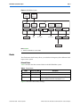
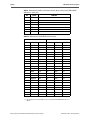
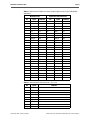
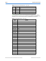
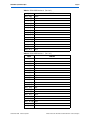
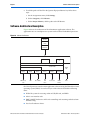
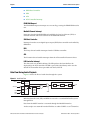
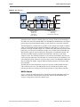
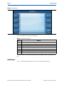
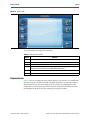
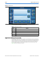
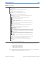
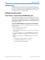
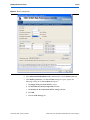
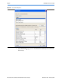
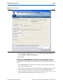
AN 533: Automotive Information and Entertainment Reference Designs AN-533-1.3 © November 2009 Introduction This application note describes automotive information and entertainment multiprocessor software reference designs for the Platform ASSP Replacement Infotainment System (PARIS) hardware reference design kit. f For more information on the PARIS kit hardware, refer to the Gleichmann AAP-PARIS1 Manual for the FPGA module and the Gleichmann MSC EXM-MBFULL R4 User's Manual for the PARIS motherboard, which are available on the CD shipped with the PARIS kit hardware. The reference designs described in this application note are examples of integration of an infotainment system-on-a-programmable-chip (SOPC) design with an Altera® FPGA device. The following reference designs are described in this application note: ■ PARIS infotainment reference design with audio playback from Secure Digital (SD) card, USB Media Oriented System Transport (MOST), and Hard Disk Drive (HDD) ■ GRACE (Graphics Controller Engine) 3D reference design with hardware-accelerated 3D graphics demo ■ GRACE video reference design with H264 video decoding The reference designs demonstrate the following functionality running on Nios® II embedded processors in Altera FPGAs: ■ Streaming encoded audio files (MP3 or WAV) from: ■ SD card—including SD high capacity (SDHC) ■ USB ■ HDD ■ MOST interface ■ Audio decoding using the Spirit DSP MP3 decoder software ■ Audio routing using the Bosch-enhanced digital audio routing (EDAR) module ■ H264 Video decoding with hardware accelerator ■ 2D and 3D graphics acceleration ■ Graphical User Interface (GUI) with LCD touchscreen f For more information, refer to the following websites: MOST interfaces: www.mostcooperation.com. Spirit DSP: www.spiritdsp.com. NetServices: www.smsc-ais.com. The reference designs use the following IP from Altera and its partners: © November 2009 Altera Corporation AN 533: Automotive Information and Entertainment Reference Designs Preliminary Page 2 System Requirements ■ Nios II processor ■ DDR2 SDRAM Controller MegaCore® function ■ LCD controller ■ Bus interfaces to on-board components: ■ EXM32 interface ■ Two I2C interfaces ■ JTAG UART ■ Flash memory interface The reference designs use the following IP from Altera’s partners: ■ Graphics accelerator: D/AVE 2D IP from TES ■ External media interfaces: ■ SD card (including SDHC) ■ USB ■ HDD ■ MediaLB interface for MOST interface ■ Audio routing by Bosch EDAR module ■ GRACE 3D reference design—D/AVE 3D IP from TES replaces the D/AVE 2D IP ■ GRACE video reference design—H264 video decoder from Videantis IP The reference designs use the following SOPC Builder components: ■ PLLs ■ DMAs ■ Timers ■ Half-rate bridge ■ Tristate bridge ■ System ID ■ On-chip memories ■ Parallel I/O interfaces System Requirements The reference designs have the following system requirements: ■ ■ PARIS kit—PARIS-1 FPGA module and EXM32 motherboard. ■ The GRACE 3D and GRACE video reference designs require a Stratix II 2S180 PARIS FPGA module. ■ The PARIS reference design is available for both Stratix II 2S90 and 2S180 PARIS FPGA modules. Quartus® II software version 9.1 and Nios II Embedded Design Suite version 9.1 AN 533: Automotive Information and Entertainment Reference Designs Preliminary © November 2009 Altera Corporation System Requirements Page 3 ■ Partner IP licenses for modifying and rebuilding the reference designs The reference designs include the following files: ■ SRAM Object File (.sof) for FPGA programming the FPGA with pre-built hardware reference designs ■ Software binary file (.elf) for running pre-built reference design software ■ Hardware modules not covered by third-party licenses (mostly SOPC Builder components) ■ Application software source code or libraries for modules not covered by thirdparty licenses ■ Build scripts for rebuilding software using the Nios II software build tools FPGA Programming Files You can configure the FPGA with the reference design from on-board flash memory at power-up, or you can download the Altera-provided .sof to the FPGA device using the Quartus II Programmer. Each reference design has its own associated .sof. You can modify and rebuild the SOPC Builder project only if you obtain the appropriate licenses for the licensed IP in the design. In most cases, OpenCore Plus licenses allow evaluation of the IP in the SOPC Builder project at no cost. f For more information on OpenCore Plus, refer to AN 320: OpenCore Plus Hardware Evaluation for Megafunctions. Software Binary Files (.elf) The reference design software applications are delivered as .elf files. These .elf files must be programmed into the on-board flash memory for execution at power-up, or downloaded using the Nios II command-line tools. Download scripts are provided with the reference design. Each reference design has its own associated .elf, which runs only on the corresponding FPGA configuration. If you change the FPGA configuration, you must recompile the design. For example, adding or removing a peripheral module, requires that you recompile the BSP (Board Support Package). f For more information on using the Nios II software build tools, refer to the Nios II Software Developer's Handbook. The software can be recompiled only if all of the appropriate libraries and source code are available to support the hardware IP. Access to some source code may require license agreements with Altera partners. Partner IP Licenses Table 1 lists the partner IP contact details. © November 2009 Altera Corporation AN 533: Automotive Information and Entertainment Reference Designs Preliminary Page 4 Installing the Reference Designs Table 1. Partner IP Contact Details IP Company Contact Hardware USB2 OTG Ingenieurbüro für IC-Technologie (IFI) www.ifi-pld.de/IP/ip.html ATA Evatronix www.evatronix.pl [email protected] SD card Eureka Technology Inc [email protected] EDAR Robert Bosch GmbH www.semiconductors.bosch.de/en/ MediaLB (MOST interface) Ingenieurbüro für IC-Technologie www.ifi-pld.de/IP/ip.html D/AVE 2D-TS TES Electronic Solutions www.tesbv.com D/AVE 3D TES Electronic Solutions www.tesbv.com MP2020 Videantis GmbH www.videantis.de USB driver Emsys www.emsys.de SD Card Driver (SDIOWorx) Embwise www.embwise.com MOST NetServices SMSC www.smsc-ais.com Audio codec (MP3 decoder) SpiritDSP www.spiritdsp.com Software Installing the Reference Designs The reference designs are contained in the paris_91.zip file. Unzip the paris_91.zip file to a directory on your computer. Extracting the paris_91.zip builds the directory structure shown in Figure 1. The directories are described in this section. 1 For more information about the reference design file directory structure and installation instructions, refer to the readme.txt file, which is located in the paris_91 directory after the files have been extracted from the paris_91.zip file. AN 533: Automotive Information and Entertainment Reference Designs Preliminary © November 2009 Altera Corporation Installing the Reference Designs Page 5 Figure 1. Reference Design Top-level Directories paris_91 Quartus grace_3D grace_video paris_2s90 paris_2s180 setup ThreadX software build grace_hmi paris_hmi source Quartus Directory The Quartus directory contains archives of the FPGA projects for the reference designs and .sof programming files for the FPGA. Each reference design is located in a separate subdirectory. Setup Directory The setup directory contains additional source files required for the ThreadX real time operating system (RTOS). If you have access to the RTOS source code and are rebuilding the reference design software applications, review and run the setup_threadx.sh script after installing RTOS. Review the script and make any necessary amendments to the QUARTUS_DIR variable, depending on the location of your Quartus IP directory. Software Directory The software directory contains the following subdirectories: © November 2009 ■ Build—contains build scripts for rebuilding the source code and libraries. The source code can be rebuilt only if all third-party licensed source code are available. Scripts for downloading .sof and .elf files to hardware are also provided. ■ Grace_hmi—contains source files for the Altia HMI project for the GRACE reference designs. ■ Paris_hmi—contains source files for the Altia HMI project for the PARIS reference designs. ■ Source—contains software source code, except software that requires third-party license agreements. For software that requires third-party license agreements, empty directories are present as place holders. Refer to “Application Software Source Code”. Altera Corporation AN 533: Automotive Information and Entertainment Reference Designs Preliminary Page 6 Downloading the Reference Designs to Hardware Downloading the Reference Designs to Hardware You can download the .sof programming files to the PARIS kit hardware with the Quartus II Programmer or with the nios2-configure-sof command in a Nios II command shell. Scripts that download the .sof and .elf files in a single step in a Nios II command shell are provided for each reference design. For example, the 2s180_paris_download_all.sh script downloads the .sof and .elf files to the /software/build/paris_2s180 directory. Copying Media Files to the Hard Disk Drive Ensure that you use the latest version of the PARIS reference design by downloading the .sof and .elf files from the paris_2s90 or paris_2s180 directory, depending on the version of your PARIS kit. To transfer files from a USB flash drive to your PARIS kit Hard Disk Drive (HDD), follow these steps: 1. Transfer the files you want to copy onto a USB flash drive. If you want to erase the HDD before copying the files, then include a file or directory named do_delete_hdd in the top-level directory. 2. Insert the USB flash drive in the lower PARIS motherboard USB port. 3. Touch AUDIO on the touchscreen. The audio screen displays. 4. On the Audio screen, touch USB. The USB screen displays. 5. On the USB screen, touch COPY. The screen displays the message "Copying to HDD." All files on the USB flash drive are copied to the root directory of the HDD, retaining the same directory structure. When the file transfer is complete, the screen displays the message "HDD Stopped." After file transfer is complete, you can remove the USB flash drive. Navigating through Directories Directory names are shown in the track list enclosed by brackets, for example, [music]. To navigate through directories, follow these steps: 1. Select the directory in the track list. 2. On the touchscreen, touch PLAY. 3. To return to a higher directory, select [..] in the track list. 4. Touch PLAY. SOPC Builder System Description This section describes the SOPC Builder system and its components. Figure 2 shows a simplified block diagram of the SOPC Builder system. AN 533: Automotive Information and Entertainment Reference Designs Preliminary © November 2009 Altera Corporation SOPC Builder System Description Page 7 Figure 2. SOPC Builder System 16-bit 533 (32 MB) DDR2 SDRAM 16-bit 16 MB Flash Memory FPGA MP20201 DDR2 SDRAM Controller Flash Interface USB Host ATA SD Card PHY HDD SD or SDHC System Nios II Processor D/AVE LCD Controller 2D or 3D1 Touchscreen Audio Nios II Processor MediaLB EDAR Audio Routing OS81050 Audio CODECs Optics Note to Figure 2: (1) D/AVE 3D and MP2020 are used in GRACE. Clocks The Gleichmann clock factory allows you to define the frequency of the different clock inputs to the system. External Clocks Table 2 describes the three external clocks in the SOPC Builder system. Table 2. External Clocks Name clk_in omck clk_ata Frequency (MHz) 50 24.576 50 Description Clock factory reference Clk0. Clock factory reference Clk13. Generated by a PLL external to the SOPC system. The clock factory reference for the PLL clock input is Clk1. Figure 3 shows the clock factory settings. © November 2009 Altera Corporation AN 533: Automotive Information and Entertainment Reference Designs Preliminary Page 8 SOPC Builder System Description Figure 3. Clock Factory Settings FPGA-Generated Clocks The 50MHz FPGA input clock is multiplied internally and distributed around the FPGA. The DDR2 SDRAM High-Performance Controller MegaCore function, described in “DDR2 SDRAM High-Performance Controller” instantiates a PLL, which generates the system clocks and the clocks required by the memory controller. Table 3 describes the clocks used in the SOPC system. Table 3. Generated Clocks Name Frequency (MHz) Description altmemddr_0_auxhalf 65 The system clock. Its frequency is half of the DDR2 SDRAM High-Performance Controller MegaCore function clock. altmemddr_0_auxfull 130 Half-rate bridge master clock. 64 × fs = 3.072 i2sclk Audio clock for I2S interface for the EDAR IP (not used). Nios II System Processor The Nios II system processor (SOPC instance cpu) runs the application software and drives all the system peripherals. The Nios II system processor is a Nios II fast processor with hardware implementation of multiplication and division, 8K data cache, and 8K instruction cache. The Nios II system processor reset vector is located at the 0x10_0000 address in the external flash memory and its exception vector is located at the 0x40_0020 address in the DDR2 SDRAM. AN 533: Automotive Information and Entertainment Reference Designs Preliminary © November 2009 Altera Corporation SOPC Builder System Description f Page 9 For more information, refer to the Instantiating the Nios II Processor in SOPC Builder chapter in the Nios II Processor Reference Handbook. Nios II Audio Processor The Nios II audio processor (SOPC instance cpu_mp3) decodes MP3 audio. The Nios II audio processor communicates with the cpu via the mp3_control_buffer. The Nios II audio processor is a Nios II fast processor with hardware implementation of multiplication and division, 8K data cache, and 8K instruction cache. The Nios II audio processor reset vector is located at the 0x00_0000 address in the external flash memory. The Nios II audio processor exception vector is located at the 0x00_0020 address in the DDR2 SDRAM. The Spirit MP3 decoder library uses Nios II custom instructions to accelerate the MP3 decode process. The PARIS and GRACE applications are supplied with an OpenCore Plus license to enable these instructions and allow evaluation of the MP3 decoder. System-to-DDR2 SDRAM Interface This section describes the system-to-DDR2 SDRAM interface. Half-Rate Bridge DDR2 SDRAMs require a high minimum operating frequency. Moreover, delays in memory accesses by the controller are dependent on the clock used for the memory controller (the faster the clock, the shorter the delay). To address these two limitations, the FPGA configuration uses a half-rate bridge. Interfaces to the DDR2 SDRAM are made through a data bus of 64-bits at a frequency driven by altmemddr_0_auxhalf. Other SOPC Builder components that do not support the 64-bit interface do not benefit from the full bus bandwidth. Figure 4 shows the half-rate bridge settings in SOPC Builder. © November 2009 Altera Corporation AN 533: Automotive Information and Entertainment Reference Designs Preliminary Page 10 SOPC Builder System Description Figure 4. Half-Rate Bridge Settings The half-rate bridge uses a set of Synopsys Design Constraints (.sdc) for timing analysis. These constraints are stored in the standard.sdc file. DDR2 SDRAM High-Performance Controller The DDR2 SDRAM High-Performance Controller MegaCore function runs at 130 MHz and interfaces only with the half-rate bridge. Two 16-bit 32MB banks of DDR2 memory are available on the FPGA module. The infotainment demonstration uses a single bank of memory. The GRACE video demonstration uses both banks of memory. Review the SOPC Builder design and the project pin assignments to determine the configuration of the two memory banks. f For more information, refer to the DDR and DDR2 SDRAM High-Performance Controller and ALTMEMPHY User Guide. External Flash The PARIS FPGA module has a 16MB flash memory. The flash interface is configured in 16-bit mode. The flash memory stores the FPGA configuration, the boot loader with default screen image for cpu, and the demonstration code running on the two Nios II processors. Table 4 describes the flash memory mapping for this system. AN 533: Automotive Information and Entertainment Reference Designs Preliminary © November 2009 Altera Corporation SOPC Builder System Description Page 11 Table 4. Flash Memory Mapping Address Range (hex) Content 000000 to 0FFFFF cpu_mp3 code 100000 to 1FFFFF cpu custom boot loader code 110000 to 1FFFFF Default screen image 200000 to 7FFFFF cpu application code 800000 to 80FFFF Options for FPGA configuration 810000 to FFFFFF FPGA configuration .sof data LCD Interface This section describes the LCD controller and the touchscreen interface. LCD Controller The LCD controller is parameterized for the 800x480 WVGA display in the package. If you want to use different display, you can change the parameters by double-clicking the parameter in the SOPC Builder as shown in Figure 5. Figure 5. LCD Controller Timing Parameters Table 5 describes the LCD controller parameters. Table 5. LCD Controller Parameters Parameter Description Device Target device (not used). Avalon interface type Type of Avalon® master interface this component is using: DEFAULT or BURST. For more details on BURST mode, refer to the Avalon Interface Specifications. © November 2009 Altera Corporation AN 533: Automotive Information and Entertainment Reference Designs Preliminary Page 12 SOPC Builder System Description Table 5. LCD Controller Parameters Parameter Description MASTER_DATA_WIDTH Width of the data bus from the three Avalon Memory-Mapped (Avalon-MM) master ports of the component. 32 or 64 bits. Timing parameters The value for different timing parameters must be set to the LCD display that you use. Figure 6 and Figure 7 show the LCD controller timing parameters. Active frame is the part when lines are displayed; active line is when the frame is active and the time when the line is displayed at a rate of one pixel per clock cycle. Figure 6. LCD Controller Timing Parameters—pixel_clk and Hsync Pixel_clk Hsync 88 clk cycles Active line 800 clk cycles 40 clk cycles 128 clk cycles HSyncEnd HBlank Begin HBlank End HLineEnd Figure 7. LCD Controller Timing Parameters—Hsync and Vsync Hsync Vsync 32 Hsync Cycles Active Frame 480 Hsync Cycles 9 Hsync Cycles 2 Hsync Cycles VSyncEnd VBlankBegin VBlankEnd VFrameEnd Touchscreen Interface The application software running on cpu drives the touchscreen interface using the I2C0 interface. Audio Interface This section describes the audio interface. AN 533: Automotive Information and Entertainment Reference Designs Preliminary © November 2009 Altera Corporation SOPC Builder System Description Page 13 Audio Routing The decoded audio PCM data is read from a location in the DDR2 SDRAM, and is written to the EDAR IP slave interface with the edar_dma. The EDAR IP routes this stereo channel to the DAC with the I2S interface 0. The application software running on cpu sets up the various IP to configure this path. Audio DAC Configuration Interface The application software running on cpu configures the DAC with the I2C1 interface. Refer to the board documentation for information regarding the DAC settings. EXM-ATA Interface The motherboard has configuration options that you can change using the EXM32 bus. This bus interface shares pins with the HDDATA interface. The EXM32 bus and the HDD interfaces use the EXM_ATA_IF top-level file. EXM_ATA_IF Ports The ATA interface uses the component clock clk_ata, which also uses altmemddr_0_auxhalf for the Avalon-MM and EXM32 bus interfaces. The ATA IP from Evatronix use the following ports: ■ ata_avalon_slave ■ ata_dma_master ■ sfr_slave ports The exm_avalon_slave port is a direct mapping of the EXM bus address space. Setting up the EXM_ATA_IF Component The Altera-provided EXM_ATA_IF component, which includes the EXM32 bus interface and the EXM_ATA_IF top-level file, is incomplete. You must obtain the ATA IP from Evatronix to use the EXM_ATA_IF component. To set-up the ATA IP, follow these steps: 1. Delete the chip_ataif.v and chip_ataif_hw.tcl files, which are located in the Evatronix src directory. 2. Copy the remaining source files from the Evatronix src directory to the exm_ata directory in your project. Third-Party Multimedia Interfaces Third-party IP partners provide the SD card, USB, and MediaLB media interfaces. The cpu application software runs these interfaces. f For more information, refer to the relevant IP documentation. USB Interface The IFI USB2 Highspeed OTG interface is shipped with timing constraints in an .sdc file that is incompatible with the PARIS architecture. © November 2009 Altera Corporation AN 533: Automotive Information and Entertainment Reference Designs Preliminary Page 14 SOPC Builder System Description To resolve the .sdc file incompatibility, perform the following steps: 1. Generate the system in SOPC builder. 2. Open the std_2s60.qip file in the Quartus II Text Editor. 3. Remove the line that refers to ifi_usb2_high_otg_const.sdc. Removing the line removes the .sdc file entry for the IFI USB2 Highspeed OTG interface. After you remove the .sdc file entry for the IFI USB2 Highspeed OTG interface from the project’s .qip file, the system uses the timing constraints that are provided in the project constraint .sdc file. Arbitration Shares To guarantee efficient access to memory, arbitration shares are used in the SOPC builder design. Nios II processors are connected to memory using arbitration shares of 8 to match the burst length of the Nios II caches, as shown in Figure 8. Figure 8. Nios II Processor Arbitration Shares The LCD controller is connected using 32 arbitration shares to match the burst length of its Avalon masters. Other masters are similarly connected using corresponding arbitration shares, as shown in Figure 9. AN 533: Automotive Information and Entertainment Reference Designs Preliminary © November 2009 Altera Corporation SOPC Builder System Description Page 15 Note that the connections to the memory are routed through a pipeline bridge and a half-rate bridge. These extra connections do not require arbitration shares because one master only is connected to each slave (pipeline bridge master to half-rate bridge slave and half-rate bridge master to DDR2 SDRAM controller slave). Figure 9. Arbitration Shares I/O Table 6 through Table 12 provide cross-references between I/O connectors on the PARIS motherboard and the corresponding FPGA pins for interfaces that connect directly to the I/O. 1 For full details of motherboard connector placement and pin orientation, refer to the Gleichmann MSC EXM-MBFULL R4 User's Manual for the PARIS motherboard. Table 6. Motherboard X24 LCD1 TTL 31-Pin FPC Connector (Part 1 of 2) Pin © November 2009 Signal FPGA Pin 1 GND n/a 2 CLK N30 Altera Corporation AN 533: Automotive Information and Entertainment Reference Designs Preliminary Page 16 SOPC Builder System Description Table 6. Motherboard X24 LCD1 TTL 31-Pin FPC Connector (Part 2 of 2) Pin Signal FPGA Pin 3 HSYNC M30 4 VSYNC M29 5 GND n/a 6 R0 G30 7 R1 G29 8 R2 H32 9 R3 H31 10 R4 H30 11 R5 H29 12 GND n/a 13 G0 F32 14 G1 F31 15 G2 F30 16 G3 F29 17 G4 G32 18 G5 G31 19 GND n/a 20 B0 D32 21 B1 D31 22 B2 E32 23 B3 E31 24 B4 E30 25 B5 E29 26 GND n/a 27 DE M32 28 VCC n/a 29 VCC n/a 30 R/L n/a 31 U/D n/a Table 7. Motherboard X38 GPIO/LCD2 50-Pin Connector Motherboard X38 GPIO Pin Signal LCD2 50-Pin Connector FPGA Pin Pin Signal FPGA Pin 1 5V n/a 2 5V -n/a 3 3.3V n/a 4 3.3V -n/a 5 I2 SCL N28 6 I2C SDA P32 7 I2 INT# n/a 8 GND n/a 9 n.c. n/a 10 GND n/a 11 D0 H28 12 D1 H27 AN 533: Automotive Information and Entertainment Reference Designs Preliminary © November 2009 Altera Corporation SOPC Builder System Description Page 17 Table 7. Motherboard X38 GPIO/LCD2 50-Pin Connector Motherboard X38 GPIO Pin Signal LCD2 50-Pin Connector FPGA Pin Pin Signal FPGA Pin 13 D2 J27 14 D3 J26 15 D4 K27 16 D5 K26 17 D6 K24 18 D7 K25 19 GND n/a 20 GND n/a 21 n.c. n/a 22 M DE K32 23 n.c n/a 24 HSYNC K30 25 VSYNC K29 26 n.c n/a 27 SHFCLK L31 28 n.c n/a 29 GND n/a 30 GND n/a 31 D8 L26 32 D9 L25 33 D10 L24 34 D11 L23 35 D12 M27 36 D13 M26 37 D14 M25 38 D15 M24 39 GND n/a 40 GND n/a 41 VDON J31 42 n.c n/a 43 VCON K31 44 n.c n/a 45 n.c n/a 46 DON L32 47 n.c n/a 48 BLON L30 49 I2C A0 n/a 50 I2CA1 n/a Table 8. Motherboard X14 COM0 9-Pin D-Sub Connector (Not currently used by PARIS/GRACE applications) Pin Signal FPGA Pin 1 DCD# n/a 2 RXD P28 3 TXD P29 4 DTR# n/a 5 GND n/a 6 DSR# n/a 7 RTS# P27 8 CTS# P26 9 RI# n/a Table 9. Motherboard X14 COM1 9-Pin D-Sub Connector (Not currently used by PARIS/GRACE applications) (Part 1 of 2) Pin © November 2009 Signal FPGA Pin 1 DCD# n/a 2 RXD P24 Altera Corporation AN 533: Automotive Information and Entertainment Reference Designs Preliminary Page 18 SOPC Builder System Description Table 9. Motherboard X14 COM1 9-Pin D-Sub Connector (Not currently used by PARIS/GRACE applications) (Part 2 of 2) Pin Signal FPGA Pin 3 TXD P25 4 DTR# n/a 5 GND n/a 6 DSR# n/a 7 RTS# P29 8 CTS# R28 9 RI n/a Table 10. Motherboard X19 PATA/ATAPI 44-Pin Connector Motherboard X38 GPIO Pin Signal LCD2 50-Pin Connector FPGA Pin Pin Signal FPGA Pin 1 RESET# n/a 2 GND n/a 3 D7 (1) 4 DS (1) 5 D6 (1) 6 D9 (1) 7 D5 (1) 8 D10 (1) 9 D4 (1) 10 D11 (1) 11 D3 (1) 12 D12 (1) 13 D2 (1) 14 D13 (1) 15 D1 (1) 16 D14 (1) 17 D0 (1) 18 D15 (1) 19 GND n/a 20 n.c. n/a 21 DMARQ L4 22 GND n/a 23 IOW# B13 24 GND n/a 25 IOR# E14 26 GND n/a 27 IORDY# C9 28 CSEL# n/a 29 DMACK# M4 30 GND n/a 31 INTRQ A7 32 n.c. n/a 33 A1 (1) 34 CBLID# n/a 35 A0 (1) 36 A2 (1) 37 CS0# E9 38 CS1# A8 39 DASP# n/a 40 GND n/a 41 5V n/a 42 FV n/a 43 GND n/a 44 Reserved n/a Note: (1) Pins shared with motherboard EXM bus. Refer to Gleichmann MSC EXM-MBFULL R4 User's Manual. AN 533: Automotive Information and Entertainment Reference Designs Preliminary © November 2009 Altera Corporation SOPC Builder System Description Page 19 Table 11. Motherboard X37 Digital Video 50-pin connector (Not currently used by PARIS/GRACE applications) Motherboard X37 Pin Signal Digital Video 50-Pin Connector FPGA Pin Pin Signal FPGA Pin 1 5V n/a 2 5V n/a 3 3.3V n/a 4 3.3V n/a 5 I2 SCL N28 6 I2C SDA P32 7 I2C INT# n/a 8 GND n/a 9 n.c. n/a 10 GND n/a 11 DV0 D0 C26 12 DV0 D1 D26 13 DV0 D2 E26 14 DV0 D3 A25 15 DV0 D4 B25 16 DV0 D5 C25 17 DV0 D6 D25 18 DV07 E25 19 GND n/a 20 GND n/a 21 n.c. n/a 22 DV0 DE AV# B22 23 n.c. n/a 24 DV0 HSYNC C22 25 DV0 VSYNC D22 26 n.c. n/a 27 DV0 CLK A22 28 n.c. n/a 29 GND n/a 30 GND n/a 31 DV1 D0 A24 32 DV1 D1 B24 33 DV1 D2 C24 34 DV1 D3 E24 35 DV1 D4 A23 36 DV1 D5 B23 37 DV1 D6 C23 38 DV1 D7 B23 39 GND n/a 40 GND n/a 41 n.c. n/a 42 DV0 DE AV# B21 43 n.c. n/a 44 DV0 HSYNC C21 45 DV0 VSYNC D21 46 n.c. n/a 47 DV0 CLK A21 48 n.c. n/a 49 I2C A0 n/a 50 I2C A1 n/a Table 12. Motherboard X23 SDIO Card Socket (Part 1 of 2) Pin © November 2009 Signal FPGA Pin 1 DAT3 N22 2 CMD N26 3 GND n/a 4 VDD n/a 5 CLK M22 6 GND n/a 7 DAT0 N25 8 DAT1 N24 9 DAT2 N23 Altera Corporation AN 533: Automotive Information and Entertainment Reference Designs Preliminary Page 20 SOPC Builder System Description Table 12. Motherboard X23 SDIO Card Socket (Part 2 of 2) Pin Signal FPGA Pin 10 CD# N27 11 COM n/a 12 WP M23 13 CHASSIS n/a 14 n.c. n/a Table 13 through Table 19 give a cross reference between signals for the remaining I/O and FPGA pins. These signals are routed through motherboard components (e.g. USB PHY) so have no direct correspondence to motherboard I/O connectors. Table 13. DDR2 SDRAM Interface 0 (Part 1 of 2) Signal FPGA Pin ddr2_0_a[0] AC15 ddr2_0_a[1] AG11 ddr2_0_a[2] AE14 ddr2_0_a[3] AD12 ddr2_0_a[4] AG16 ddr2_0_a[5] AD13 ddr2_0_a[6] AC16 ddr2_0_a[7] AE13 ddr2_0_a[8] AL16 ddr2_0_a[9] AL11 ddr2_0_a[10] AB13 ddr2_0_a[11] AL13 ddr2_0_a[12] AK13 ddr2_0_ba[0] AB14 ddr2_0_ba[1] AC14 ddr2_0_cas_n AD14 ddr2_0_cke[0] AK11 ddr2_0_clk[0] AJ15 ddr2_0_clk_n[0] AH15 ddr2_0_cs_n[0] AM16 ddr2_0_dm[0] AH16 ddr2_0_dm[1] AH14 ddr2_0_dq[0] AK12 ddr2_0_dq[1] AM11 ddr2_0_dq[2] AH11 ddr2_0_dq[3] AM12 ddr2_0_dq[4] AL10 ddr2_0_dq[5] AJ12 AN 533: Automotive Information and Entertainment Reference Designs Preliminary © November 2009 Altera Corporation SOPC Builder System Description Page 21 Table 13. DDR2 SDRAM Interface 0 (Part 2 of 2) Signal FPGA Pin ddr2_0_dq[6] AM10 ddr2_0_dq[7] AJ11 ddr2_0_dq[8] AJ14 ddr2_0_dq[9] AG13 ddr2_0_dq[10] AJ13 ddr2_0_dq[11] AH13 ddr2_0_dq[12] AF13 ddr2_0_dq[13] AG15 ddr2_0_dq[14] AM14 ddr2_0_dq[15] AL14 ddr2_0_dqs[0] AK10 ddr2_0_dqs[1] AG14 ddr2_0_odt[0] AB16 ddr2_0_ras_n AB15 ddr2_0_we_n AL12 Table 14. DDR2 SDRAM Interface 1 (Part 1 of 2) Signal FPGA Pin ddr2_1_a[0] AH9 ddr2_1_a[1] AH7 ddr2_1_a[2] AG9 ddr2_1_a[3] AJ5 ddr2_1_a[4] AE11 ddr2_1_a[5] AL4 ddr2_1_a[6] AL8 ddr2_1_a[7] AM4 ddr2_1_a[8] AF11 ddr2_1_a[9] AK5 ddr2_1_a[10] AH6 ddr2_1_a[11] AL9 ddr2_1_a[12] AG8 ddr2_1_ba[0] AH5 ddr2_1_ba[1] AL6 ddr2_1_cas_n AE10 ddr2_1_cke[0] AK4 ddr2_1_clk[0] AL15 ddr2_1_clk_n[0] AK15 © November 2009 ddr2_1_cs_n[0] AD11 ddr2_1_dm[0] AC13 Altera Corporation AN 533: Automotive Information and Entertainment Reference Designs Preliminary Page 22 SOPC Builder System Description Table 14. DDR2 SDRAM Interface 1 (Part 2 of 2) Signal FPGA Pin ddr2_1_dm[1] AE12 ddr2_1_dq[0] AM7 ddr2_1_dq[1] AK7 ddr2_1_dq[2] AM6 ddr2_1_dq[3] AM5 ddr2_1_dq[4] AJ7 ddr2_1_dq[5] AM8 ddr2_1_dq[6] AK6 ddr2_1_dq[7] AJ6 ddr2_1_dq[8] AG10 ddr2_1_dq[9] AK8 ddr2_1_dq[10] AJ10 ddr2_1_dq[11] AF10 ddr2_1_dq[12] AJ8 ddr2_1_dq[13] AG12 ddr2_1_dq[14] AM9 ddr2_1_dq[15] AF12 ddr2_1_dqs[0] AL5 ddr2_1_dqs[1] AK9 ddr2_1_odt[0] AC12 ddr2_1_ras_n AL7 ddr2_1_we_n AH8 Table 15. USB2.0 Interface 0 Signal FPGA Pin usb0_clkout U1 usb0_data[0] W2 usb0_data[1] W1 usb0_data[2] V5 usb0_data[3] V4 usb0_data[4] V3 usb0_data[5] V2 usb0_data[6] U6 usb0_data[7] U5 usb0_dir Y2 usb0_nxt W2 usb0_reset Y3 usb0_stp W4 usb0_oc Y4 AN 533: Automotive Information and Entertainment Reference Designs Preliminary © November 2009 Altera Corporation Setting Up the Environment Page 23 Table 16. USB2.0 Interface 1 Signal FPGA Pin usb0_clkout U3 usb0_data[0] AB4 usb0_data[1] AB3 usb0_data[2] AB2 usb0_data[3] AB1 usb0_data[4] AA4 usb0_data[5] AA3 usb0_data[6] AA2 usb0_data[7] AA1 usb0_dir AC2 usb0_nxt AC1 usb0_reset AC3 usb0_stp AB5 Table 17. MediaLB Interface Signal FPGA Pin mlbclk C27 mlbdat B26 mlbsig E27 Table 18. I2C0 Interface Signal FPGA Pin i2c0_scl R31 i2c0_sda P31 Table 19. I2C1 Interface Signal FPGA Pin i2c1_scl P32 i2c1_sda N28 Setting Up the Environment To set your Quartus II environment to use the PARIS reference design, perform the following steps to obtain the necessary licenses for third-party IP, and set up the Quartus II software to find the IP and the licenses. 1. Add licenses to the LM_LICENSE_FILE environment variable, or manually add them in the License Setup page of the Options dialog box in the Quartus II software. © November 2009 Altera Corporation AN 533: Automotive Information and Entertainment Reference Designs Preliminary Page 24 Software Architecture Description 2. To add the path to all the IP in the Quartus II project libraries list, follow these steps: a. On the Assignments menu, click Settings. b. Under Categories, click Libraries. c. Under Project Libraries, add the paths to the IP libraries. Software Architecture Description Figure 10 shows the architecture of the infotainment application software. The application runs on a multiprocessor system with two Nios II embedded processors. Figure 10. Software Architecture MP3 Decoder Spirit DSP Library Nios II Custom Instructions Nios II Processor Altia NetServices V2 RTOS Abstraction Layer ThreadX RTOS EDAR HSL File X FAT32 File System USB Host Drivers ATA Drivers SD Card Drivers D/AVE Drivers Touchscreen Drivers MediaLB Low Level Driver USB Memory Stick HDD SD or SDHC LCD Panel Touchscreen MOST Interface Audio One Nios II processor runs the main application software using the ThreadX real time operating system (RTOS). Lower-level layers of the software include the following items: ■ FAT32 file system for accessing audio on USB, SD card, and HDD ■ Altia’s user interface tools ■ SMSC’s MOST NetServices API v2 for controlling and streaming audio data from the MOST ring ■ Low-level hardware drivers AN 533: Automotive Information and Entertainment Reference Designs Preliminary © November 2009 Altera Corporation Software Architecture Description Page 25 The second Nios II processor decodes MP3 audio using the Spirit DSP MP3 decoder software. Nios II custom instructions accelerate critical parts of the MP3 decoder software. Data transfer between the two Nios II processors occurs via the system’s DDR2 SDRAM. Control and status information is passed via the MP3 control buffer, which is a small on-chip buffer implemented in a single M4K memory. This buffer has a known base address (defined in the SOPC Builder project), which can be determined from the system library system description file, system.h. An RTOS abstraction layer simplifies porting the application to a different RTOS. Initialization The C main() function starts the ThreadX kernel. The ThreadX callback function tx_application_define() creates a number of threads and other resources used by the application. Some threads begin execution immediately, while other threads are created, but not started until further initialization is complete. Threads This section describes the following threads: ■ Initialization Thread ■ EDAR ISR Thread ■ File Reader Thread ■ NetServices Service Thread ■ NetServices Trace Thread ■ NetServices Application CD Thread ■ NetServices Application Thread ■ Debug Thread ■ Infotainment Application Thread ■ MP3 Nios II Threads Initialization Thread The initialization thread, thread_0, executes immediately after creation. This thread calls the initialization functions for the low level hardware drivers and also for NetServices. The following initialization occurs: © November 2009 ■ Initialize audio CODEC ■ Initialize EDAR ■ Initialize EDAR DMA ■ Initialize infotainment application (data structures, buffers) and start infotainment application thread ■ Initialize NetServices required resources (mutex, event flags) Altera Corporation AN 533: Automotive Information and Entertainment Reference Designs Preliminary Page 26 Software Architecture Description ■ Initialize MediaLB device interface macro (DIM) and low level drivers (LLDs) ■ Start NetServices application thread: ■ Resume NetServices trace thread ■ Resume NetServices service thread ■ Resume NetServices application thread ■ Call InitNetServices() The initialization thread is suspended when initialization is complete. EDAR ISR Thread The EDAR interrupt service routine (ISR) thread is initiated by an event flag that is set by the EDAR ISR. The thread launches a DMA to transfer decoder samples from the MP3 decoder to the EDAR input FIFO. The EDAR ISR thread is started automatically once created. File Reader Thread The file reader thread reads data from the file system (SD card, USB, or HDD) as required, to keep the file buffer populated with data for the MP3 decoder. The file reader thread is created in a suspended state. The thread resumes when a file is played and is suspended again when the file play ends. NetServices Service Thread The NetServices service thread runs periodically to call NetServices functions, MostService() and Most CheckTimers(), or to service requests from the MediaLB low-level driver. The service thread is created in a suspended state. The thread resumes when the call to InitNetServices() completes. NetServices Trace Thread The NetServices trace thread outputs NetServices trace (debug) information to the Nios II console via the JTAG UART. f For more information on selecting the level of trace detail, refer to the NetServices documentation from SMSC. The trace thread is created in a suspended state. The thread resumes when the NetServices application thread is started and is never suspended. NetServices Application CD Thread When you select MOST audio playback in the GUI, the NetServices application CD thread (most_app_cd_thread) starts (from thread_0) when NetServices initializes and the NetServices service thread starts. When the SMSC DVDPlayer 4 MOST detects activity on the MOST ring it ejects and then reloads any disc that is already present. The CD thread sets up a streaming data connection and waits until the disc is loaded. AN 533: Automotive Information and Entertainment Reference Designs Preliminary © November 2009 Altera Corporation Software Architecture Description Page 27 The CD thread is created in a suspended state. The thread resumes when you select MOST audio playback in the GUI; the NetServices application starts and is never suspended. NetServices Application Thread The NetServices application thread runs periodically to service the NetServices application state machine through the app_run() function call. The state machine runs communication between the application and NetServices. The NetServices application thread is created in a suspended state and resumes with the app_start() function call from thread_0. Debug Thread The debug thread receives messages through a buffer in the SDRAM to be sent to the JTAG UART for display in the host system's console window. This buffer allows non-blocking, thread-safe I/O for debug messages from other threads. The debug thread suspends when no messages are waiting to be sent. Transmission of debug messages prevents the GUI thread from running and affects the GUI update rate. Messages from the debug thread are interleaved with messages from the NetServices trace thread (if enabled). Infotainment Application Thread After completing initialization of data, GUI display, and establishing communication with the MP3 decoder, the infotainment application is a simple loop that performs the following tasks: ■ Polls for touchscreen activity ■ Calls user interface code to display the GUI based on current activity The appropriate action function is called in response to touchscreen activity. For example, to select the audio source or start playback, and so on. These functions run in the infotainment application thread. When all user requested activity is complete, the infotainment application thread sleeps for 200 ms. MP3 Nios II Threads The MP3 decoder Nios II processor runs two threads. One is functionally identical to the debug thread on the application, as described in “Debug Thread”. The main thread initializes required data, initializes the SpiritDSP library, waits for communication from the Nios II application, and then runs in an endless loop accepting commands (for example, play or stop) from the Nios II application and calling the Spirit DSP MP3 decoder when required. Interrupts This section describes the following interrupts: © November 2009 ■ EDAR DMA Request ■ MediaLB Channel Interrupt Altera Corporation AN 533: Automotive Information and Entertainment Reference Designs Preliminary Page 28 Software Architecture Description ■ SDIO Host Controller ■ USB ■ ATA ■ LCD Controller Interrupt EDAR DMA Request The EDAR DMA request interrupt sets an event flag, causing the EDAR ISR thread to run. MediaLB Channel Interrupt Interrupts from the MediaLB DIM are handled by the low-level drivers (LLD) to maintain transmit and receive buffers for the MediaLB channels. SDIO Host Controller Interrupts from the secure digital input output (SDIO) host controller are handled by SDIOWorx. USB The Emsys driver handles interrupts from the USB host controller. ATA The Evatronix driver handles interrupts from the ATA controller Evatronix driver. LCD Controller Interrupt The Altia code uses double buffering. The ISR updates the frame buffer to be displayed by the LCD controller. The ISR is part of the Altia library and it uses the default LCD controller driver provided with the D/AVE IP. Data Flow During Audio Playback Figure 11 shows the flow of audio data through the system. Figure 11. Audio Data Flow MOST MLB Net Services SD Card SDIO Worx EDAR FIFO USB USB Hard Disk HDD FileX Spirit DSP MP3 Decoder (not WAV) ARU I2S I2S WAV MP3 data from SD card, USB, and HDD is accessed as a standard FAT32 file system through FileX. Data from the MOST interface is streamed through the MediaLB interface. Audio samples are streamed from the EDAR to an audio CODEC via an I2S interface. AN 533: Automotive Information and Entertainment Reference Designs Preliminary © November 2009 Altera Corporation Software Architecture Description Page 29 MP3 Decoder MP3 decoding utilizes the SpiritDSP MP3 decoder libraries. A dedicated Nios II embedded processor is instantiated in the system to run this software. Nios II custom instructions accelerate the MP3 decoding. MP3 encoded input samples are passed through a circular buffer in SDRAM. The main system processor replenishes data in this buffer (the file reader thread) as it is consumed by the MP3 decode process. Decoded output samples are passed through a second circular buffer in SDRAM. The output buffer is large enough to hold 1,024 samples. Whenever there is sufficient space in the buffer for 384 samples, the SpiritMP3 decode routine is called. Control and status buffers are located in FPGA on-chip M4K memory (512 bytes) instantiated in the SOPC Builder project, which allows the base address of the buffers to be determined at software compile time. Pointers to the input and output buffers are passed to the MP3 decoder thread through the control buffer. Figure 12 shows the SpiritDSP MP3 decoder process. Figure 12. Spirit DSP MP3 Decoder Process Input Buffer Spirit DSP MP3 Decoder Control Buffer Output Buffer Status Buffer Nios II MP3 Decoder Nios II System Memory Bandwidth Discussion – Dual Nios II system Figure 13 shows an expanded view of the data flow in the system when decoding MP3 audio from the SD card. The system implements a pull model where data is pulled through at a rate determined by the I2S data rate from the EDAR. The EDAR FIFO can be shared by multiple streams (up to 8) with a maximum depth (if only one stream) of 1K words (1,024 samples comprising 512 left and 512 right channels for a stereo stream). To allow for future use of multiple streams being handled by EDAR, the FIFO for decoded MP3 data is restricted (somewhat arbitrarily) to 192 samples with a low watermark (LWM) at 64 samples. The FIFO is refilled in response to the LWM interrupt with a DMA transfer of 128 samples. © November 2009 Altera Corporation AN 533: Automotive Information and Entertainment Reference Designs Preliminary Page 30 Software Architecture Description Figure 13. MP3 Data Flow FileX/SDIO Worx SD Card Spirit DSP MP3 Process callback() Eureka SDIO Host File Buffer MP3 Data DMA 128 bytes decode() PCM Buffer 2,304 bytes EDAR Buffer 2,048 bytes EDAR DDR SDRAM MP3 Bitstream 320 kbps max (plus headers around 500 Kbps) 16-bit Stereo PCM Samples at 48 kHz (around 200 KBps) LWM of 32 stereo samples at 48 kHz allows for a latency of 666 s from interrupt to first DMA data received in EDAR FIFO. The EDAR deferred ISR thread is the highest priority thread, apart from IRQ handling, so this allowance is more than adequate. The EDAR buffer is partitioned into 16 buffers of 128 samples (the length of a DMA), which are filled from the Spirit DSP PCM buffer by calling the SpritMP3decode() function. If enough decoded samples are available in the MP3 decoders internal PCM buffer, they are returned. If insufficient samples are available in the PCM buffer, the MP3 decoder requests more encoded data, through the read callback function, and decodes more MP3 samples. The MP3 decoder decodes 576 stereo (1,152 total) samples at once. The decoded PCM data are stored in the PCM buffer, until they are retrieved by the application. The file buffer is a circular buffer and is refilled by a call to the FileX file system whenever at least 512 bytes are free. The SDIOWorx SDIO host drivers refill the file buffer, using the DMA controller function in the Eureka SDIO host controller. The MP3 data and the PCM buffers are private resources within the MP3 decoder with no direct user access. The MP3 decoder loads/unloads these buffers using pointers provided as parameters in the decode function and the callback function. WAV File Playback Figure 14 shows the simpler data flow for WAV file playback. DMA direct from the SDIO host controller to the EDAR is not possible, because the EDAR FIFO port occupies a single data word in the address space. AN 533: Automotive Information and Entertainment Reference Designs Preliminary © November 2009 Altera Corporation Software Architecture Description Page 31 Figure 14. WAV Data Flow FileX/SDIO Worx SD Card Eureka SDIO Host DMA 128 bytes File Buffer EDAR DDR SDRAM 16-bit Stereo PCM Samples at 48 kHz (around 200 KBps) Audio Playback from the MOST Interface Playback of CD audio is very similar to that of WAV file playback from SD card (see Figure 14). GRACE 3D Graphics Application The GRACE (Graphics Controller Engine) 3D graphics application builds upon the infotainment application with the addition of 3D graphics demos. The 3D graphics demo have no additional threads or interrupt sources. The software build scripts for the GRACE video application include additional source files and enable features in the existing source code through conditional compilation. While the 3D demo is running, each loop of the Infotainment Application Thread, as described in “Infotainment Application Thread” on page 2–27 causes the demo function to draw the next frame of the 3D display. The 3D demos are built upon the OpenGL-ES library for the D/AVE 3D graphics accelerator. Texture files for the display objects must be copied to the HDD in a directory named textures\compressed before the demos can be run. GRACE Video Application The GRACE Video application builds upon the infotainment application with the addition of H264 video playback. The audio playback software infrastructure is used for video playback with no additional threads or interrupts. The software build scripts for the GRACE video application include additional source files and enable features in the existing source code through conditional compilation. The additional source code files for the GRACE video application include the firmware that must be downloaded to the Videantis H.264 decoder. The audio and video streams are read separately from files on the HDD. The two streams must use the same filename, the H.264 encoded video with a .264 file extension, and the audio encoded as MP3 audio with a .mp3 file extension. © November 2009 Altera Corporation AN 533: Automotive Information and Entertainment Reference Designs Preliminary Page 32 Using the LCD GUI Decoded video frames are written directly to a frame buffer for display by the LCD controller. All three layers of the LCD controller (two display layers and one alpha layer) are activated for the GRACE video application. The alpha layer is written during operation to allow the user interface to be overlaid on top of the video. Using the LCD GUI You interact with the application via a GUI on the LCD touchscreen. Splash Screen Figure 15 shows the splash screen that displays on initial power-up, and while the application is loading. The splash screen displays logos and names of infotainment hardware and software IP partners. Figure 15. Splash Screen Application Screen Figure 16 shows the application screen, which displays when the application loads. AN 533: Automotive Information and Entertainment Reference Designs Preliminary © November 2009 Altera Corporation Using the LCD GUI Page 33 Figure 16. Application Screen Table 20 describes the application screen functions. Table 20. Application Screen Functions Button Function AUDIO Displays the audio screen. SETUP Displays the setup screen. Other buttons The VIDEO button, which displays a list of available tracks, is available in the GRACE video reference design. The remaining buttons in the application screen are non-functional for the PARIS reference design. Setup Screen Figure 17 shows the setup screen, which allows you to set various application parameters. © November 2009 Altera Corporation AN 533: Automotive Information and Entertainment Reference Designs Preliminary Page 34 Using the LCD GUI Figure 17. Setup Screen Table 21 describes the setup screen functions. Table 21. Setup Screen Functions Button Function Hour + Move the displayed time forward by 1 hour. Hour – Move the displayed time backward by 1 hour. 12/24 Toggle the time display between 12 and 24 hour modes. Min + Move the displayed time forward by 1 minute. Min – Move the displayed time backward by 1 minute. Labels Toggle the text labels on the GUI buttons on or off. BACK Return to the application screen. The time display is a simulated clock and resets to 13:00 each time the application is run. Audio Screen Figure 18 shows the audio screen where you can select the audio source. AN 533: Automotive Information and Entertainment Reference Designs Preliminary © November 2009 Altera Corporation Using the LCD GUI Page 35 Figure 18. Audio Screen Table 22 describes the audio screen functions. Table 22. Audio Screen Functions Button Function SD Select SD card as the audio source. USB Select USB (memory stick) as the audio source. HDD Select HDD as audio the source. MOST Select the MOST network as the audio source. The infotainment application supports playback from CD audio discs in an SMSC DVD4 MOST player. VOL + Increase the audio volume. VOL – Decrease the audio volume. Playback Screen Figure 19 shows the playback screen, which displays a list of tracks, if available from the selected source. For SD card, USB, and HDD, the media is searched for audio in MP3 or WAV format. The screen displays the list of files. The highlight bar in the middle of the screen displays the current track. For audio from the MOST network, the highlight bar displays only the currently playing track number. © November 2009 Altera Corporation AN 533: Automotive Information and Entertainment Reference Designs Preliminary Page 36 Application Software Source Code Figure 19. Playback Screen Table 23 describes the playback screen functions. Table 23. Playback Screen Functions Button Function ▲ Scroll tracklist up. ▼ Scroll tracklist down. >|| Toggle between play and pause. ■ Stop playback. << Skip one track forward. >> Skip one track backward. Application Software Source Code Recompiling the application source requires you to obtain licensed source code from a number of third-party vendors in addition to the source code that is supplied with the reference designs. The software project delivered with the infotainment application contains empty directories, which are place-holders for the licensed source code. Figure 20 shows the directory structure. AN 533: Automotive Information and Entertainment Reference Designs Preliminary © November 2009 Altera Corporation Application Software Source Code Page 37 Figure 20. Directory Structure software Top-level project directory. build Contains build scripts for reference design BSPs, libraries, and applications. grace_hmi Contains Altia project files for the GRACE 3D user interface. paris_hmi Contains Altia project files for the PARIS and GRACE Video user interface. source Contains the boot_loader, common, grace, mp3, and paris subdirectories. boot_loader Contains source code for the custom bootloader used by the PARIS and GRACE reference designs when programmed into flash memory. common Contains the emsys, Evatronix, HSL, include, ParisNetServices, ParisNetServicesApp, ParisNetServicesLLD, and SDIOWorx subdirectories. emsys This directory is empty and is a place holder for the USB host controller core, which you must license from Emsys (www.emsys.de). evatronix This directory is empty and is a place holder for the ATA host controller, which you must license from Evatronix (www.evatronix.pl) hsl Contains dource files for the Bosch EDAR Hardware Support Layer, which requires a license. include Contains include files for the application, but not those related to NetServices. ParisNetServices Contains ParisNetServices subdirectories. ParisNetServicesApp Contains C source code and include files for the NetServices application for streaming audio data from a SMSC DVDPlayer 4 MOST across the MOST network. Also contains NetServices include files which must be used in place of the default files delivered with NetServices (adjust1.h, adjust2.h). ParisNetServicesLLD Contains the low-level driver (LLD) software for the SMSC OS62400 MediaLB DIM. The LLD is originally available from the SMSC website but this version is modified to be specific to the PARIS platform. SDIOWorx This directory is empty and is a place-holder for third-party software that you must license from EmbWise. You must use the sd_FileX_App.c provided with the PARIS application (in the top level directory), grace Contains source code specific to the GRACE 3D and GRACE Video reference designs. mp3 Contains C source code, mp3_main.c, for the MP3 decoder function running on the mp3_nios Nios II processor. paris Contains source code specific to the PARIS reference design. The infotainment application requires the following other third-party software: f © November 2009 ■ Express Logic ThreadX RTOS ■ Express Logic FileX file system ■ Altia Design and Deepscreen For more information on Express Logic software, refer to www.rtos.com. For more information on Altia software, refer to www.altia.com. Altera Corporation AN 533: Automotive Information and Entertainment Reference Designs Preliminary Page 38 Modifying the Reference Designs RTOS Abstraction Layer The RTOS abstraction layer simplifies the task of porting the demonstration to an RTOS other than Express Logic ThreadX, by collecting all ThreadX-specific function calls into two C modules named user_os.c and app_os.c. Wrapper functions make the ThreadX-specific function calls available to the application. You need to edit only these wrapper functions to use a different RTOS. Modifying the Reference Designs Hardware Example 1 - Enabling the Second DDR2 SDRAM Memory Bank The PARIS FPGA module supports two banks of DDR2 SDRAM memory, but only one bank is used in the infotainment design. To use the second bank, as you would with the GRACE video application, you must add a second DDR2 high-performance controller to the SOPC Builder project, configure the new controller, and then update port connections. Use the procedures in this section to add and enable the second DDR2 SDRAM memory bank. Adding a Second DDR2 SDRAM High Performance Controller in the SOPC Builder Perform the following steps to add a second DDR2 high-performance controller to the SOPC Builder project: 1. Open your project in the Quartus II software. 2. Open the standard.bdf schematic file. 3. Double-clicking the std_2s60 instance in the schematic to open the component in the SOPC Builder. 4. On the System Contents tab, double-click DDR2 SDRAM High Performance Controller under SDRAM in the Component list. The MegaWizard interface appears. 5. Specify the following settings on the Memory Settings page under General Settings. a. In the PLL reference clock frequency box, type 50 MHz. b. In the Memory clock frequency box, type 130 MHz. c. Set Local interface clock frequency to Full. AN 533: Automotive Information and Entertainment Reference Designs Preliminary © November 2009 Altera Corporation Modifying the Reference Designs Page 39 Figure 21. Memory Settings Page 6. Select Micron MT47H16M16BG-37E in the Presets list under Memory Presets. 7. Click Modify parameters. The Preset Editor dialog box opens. Specify the following settings in the Preset Editor dialog box: a. Set Output clock pairs from FPGA to 1 pair. b. Set Total Memory interface DQ width to 16 bits. c. Set Memory on-die termination (ODT) setting to 50 ohm. d. Click OK. e. Click the PHY Settings tab. © November 2009 Altera Corporation AN 533: Automotive Information and Entertainment Reference Designs Preliminary Page 40 Modifying the Reference Designs Figure 22. Preset Editor Dialog Box 8. On the PHY Settings page, turn on Instantiate DLL externally under Advanced PHY Settings. AN 533: Automotive Information and Entertainment Reference Designs Preliminary © November 2009 Altera Corporation Modifying the Reference Designs Page 41 Figure 23. PHY Settings Page 9. On the Controller Settings page, turn on Use clocks from another controller under Multiple Controller Clock Sharing. 10. Click Finish. Configuring the DDR2 SDRAM High-Performance Controller MegaCore Function To configure the DDR2 SDRAM high-performance controller, perform the following steps: 1. In the Connections pane, move the new controller instance directly underneath the existing controller instance. 2. Create a connection between the new controller instance and the master port of the half rate bridge by clicking the connection dot in the Connections column. 3. Create connections between the new controller clock inputs and the sources of the existing controller instance clock inputs as shown in Figure 24. © November 2009 Altera Corporation AN 533: Automotive Information and Entertainment Reference Designs Preliminary Page 42 Modifying the Reference Designs Figure 24. Second DDR2 SDRAM High-Performance Controller MegaCore function Instance 4. Once the connections are made, you must reparametrize the master port of the half-rate bridge. Double-click the ssg_aim_half_rate_adapter_burst_master_0 instance in the Connections pane. The MegaWizard interface appears. 5. Under Upstream Settings and Downstream Settings, increase the master and slave address widths by one bit. Figure 25. Reparameterized Half Rate Bridge 6. Click Finish. 7. Once you have finished editing the design, for example, adding or removing other components, you may need to change the address map to accommodate the extra memory. You can change the address map by editing values in the Base column in the System Contents tab. 8. Once you have completed all modifications to the design, click Generate. 1 You must rebuild the BSP if you make any changes to the address map. AN 533: Automotive Information and Entertainment Reference Designs Preliminary © November 2009 Altera Corporation Modifying the Reference Designs Page 43 Updating the Port Connections After the SOPC system generates, you can update the port connections of the std_2s60 instance. Perform the following steps to update the port connections: 1. Open the std_2s60 instance in the Quartus II Block Editor. 2. Connect the dqs_delay_ctrl_export_from_the_altmemddr_0[5..0] output of the original controller to the dqs_delay_ctrl_import_to_the_altmemddr_0[5..0] input of the second controller. 3. Connect the global_reset_n_to_the_altmemddr_1 input of the second controller to the pld_clr_n signal. 4. Add appropriate I/O symbols to the second SDRAM DDR2 high-performance controller as shown in Figure 26. Figure 26. SDRAM DDR2 Controller Connections 5. Add the I/O assignments in Table 14 for the second SDRAM DDR2 highperformance controller with the Quartus II Assignment Editor. 6. Open the altmemddr_1_pin_assignments.tcl file in the Text Editor and make the following edits: ■ Set SOPC mode to NO. ■ Set pin_prefix to ddr2_. ■ Set mem_addr_pin_name to ${pin_prefix}a. 7. Run the altmemddr_1_pin_assignments.tcl Tcl script. © November 2009 Altera Corporation AN 533: Automotive Information and Entertainment Reference Designs Preliminary Page 44 Modifying the Reference Designs 8. If you are using the IFI USB2 Highspeed OTG, open the std_2s60.qip file in the Text Editor and remove the line that refers to ifi_usb2_high_otg_const.sdc. 9. On the Processing menu, click Start Compilation. Hardware Example 2 - Adding a Second LCD Controller Perform the following steps to add a second LCD controller to the SOPC Builder project: 1. Use the procedures described in “Hardware Example 1 - Enabling the Second DDR2 SDRAM Memory Bank” to add a second instance of the variable_2layer_lcd_controller_nbc component, except parameterize the component according to the requirements of the new display. For example, Figure 27 shows the parameterization for the 800x480 WVGA displays supplied with the PARIS kit. 2. Edit the schematic to accommodate the new symbol and add the new I/O connections. The required I/O assignments for the second display, using the 50pin connector X38 on the PARIS motherboard, are given in Table 7 on page 16. 3. Compile the Quartus II project. Figure 27. LCD Controller Parameterization for 800x480 PARIS Display AN 533: Automotive Information and Entertainment Reference Designs Preliminary © November 2009 Altera Corporation Modifying the Reference Designs Page 45 Software Example - Adding the File Copy Function This section describes the method used for adding the file copy function to the PARIS infotainment application, which allows you to copy media files from USB or SD memory to the Hard Disc Drive (HDD). The file copy function already exists in the PARIS infotainment application, so you do not need to perform the steps described in this section; however, you can adapt this procedure to add your own functions. Part 1 - Modifying the Altia User Interface 1 Familiarity with the Altia design tools is helpful with adding the file copy function with the Altia user interface. 1. Designate a button for the copy function—The audio screen, shown on Figure 18, has a blank button, which is the third button down on the right of the screen. The blank button is used to select the copy function. 2. Create new button images—Two new button images are created by editing the existing song_r3_blank_down and song_r3_blank_up blank images files to song_r3_copy_down and song_r3_copy_up, respectively, to represent the COPY button in up and down states. See Figure 28. Figure 28. Copy Button Up and Down States Up Down The blank images for the Song_r3 button are replaced by the new images in the Altia project. The new code for the user interface was generated using the code generation menu in the Altia tools. Part 2 - Modifying the Software 1. Activate the copy function—To implement the copy function, the new COPY button must be activated by touching the new COPY button on the COPY screen, which must be detected by the software. Then the selected source (SD or USB) must be parsed to find all files (including those in subdirectories) and copy them to the HDD. 2. Add the new buttons to the enums in the gui_buttons.h file—The source files gui_buttons.h and gui_buttons.c define the action taken when a touchscreen button is activated. The new button is added to the e_action and e_button enums (AUDIO_DOWNLOAD and BUTTON_DOWNLOAD respectively) in the gui_buttons.h file. The action_button and button_select arrays are similarly augmented with the new enum values. © November 2009 Altera Corporation AN 533: Automotive Information and Entertainment Reference Designs Preliminary Page 46 Modifying the Reference Designs 3. Decode the button action—To decode the button action, the AUDIO_DOWNLOAD case is added to the switch statement in the action_function() function in gui_buttons.c file. The code added for this case stops the current track playing (if any), calls a function to copy the files, and then displays the new contents of the HDD. 4. Add the copy function to the paris_hdd.c source file—The new copy function copy_to_hdd() is added to the paris_hdd.c source file. This function first searches for a directory entry (that is, a directory or file name) do_delete_hdd. If such a directory entry is found, then the HDD contents are deleted before the new files are copied. The del_all_files() and copy_all_files() functions are not documented here, and are located in the user_fs.c source file. Rebuilding the Hardware Projects To regenerate the hardware projects in the SOPC Builder and compile them in the Quartus II software, you must have access to all of the third-party IP required for your modified design. Rebuilding the Software Projects The reference design package includes build scripts for all of the software applications to make rebuilding software projects easy. The build scripts are described in this section. Rebuild the BSP If you modify the design in SOPC Builder, you must rebuild the Board Support Package (BSP). For example, for the paris 2s180 reference design, you must run the build_bsp_2s180_paris.sh and build_bsp_2s180_paris_mp3.sh scripts to build the BSPs for the main system Nios and the MP3 decoder Nios. These scripts are located in the software\build\paris_2s180 directory. Rebuild the Libraries Once you have built the BSP, you can rebuild the libraries. The NetServices library is common to all projects and the build script is located in the software\build\libs directory. Other library build scripts are located in project-specific directories, for example, software\build\paris_2s180\libs. Rebuild the Application Once you have updated the BSP and libraries, you can rebuild the applications by using scripts provided in the project-specific directories. For the PARIS 2S180 example, run the build_2s180_paris.sh and build_2s180_paris_mp3.sh scripts. Follow the instructions in “Downloading the Reference Designs to Hardware” to download your new .sof and .elf to the PARIS kit hardware. AN 533: Automotive Information and Entertainment Reference Designs Preliminary © November 2009 Altera Corporation Document Revision History Document Revision History Table 24 shows the revision history for this application note. Table 24. Document Revision History Date and Document Version October 2009 v2.1 October 2008 v2.0 101 Innovation Drive San Jose, CA 95134 www.altera.com Technical Support www.altera.com/support Changes Made ■ Added GRACE demonstration designs ■ Added examples of modifying the design ■ Added I/O pinouts ■ Renamed to the infotainment application ■ Corrected audio dataflow diagram Summary of Changes — — July 2008 v1.1 Corrected directory structure. — July 2008 v1.0 First release. — Copyright © 2008 Altera Corporation. All rights reserved. Altera, The Programmable Solutions Company, the stylized Altera logo, specific device designations, and all other words and logos that are identified as trademarks and/or service marks are, unless noted otherwise, the trademarks and service marks of Altera Corporation in the U.S. and other countries. All other product or service names are the property of their respective holders. Altera products are protected under numerous U.S. and foreign patents and pending applications, maskwork rights, and copyrights. Altera warrants performance of its semiconductor products to current specifications in accordance with Altera's standard warranty, but reserves the right to make changes to any products and services at any time without notice. Altera assumes no responsibility or liability arising out of the application or use of any information, product, or service described herein except as expressly agreed to in writing by Altera Corporation. Altera customers are advised to obtain the latest version of device specifications before relying on any published information and before placing orders for products or services.