1
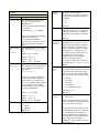
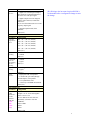
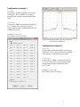
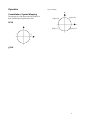
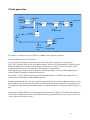
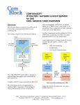
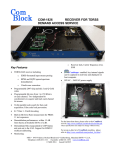
COM-1505SOFT INTEGRATED PSK MODEM VHDL source code overview / IP core o Overview Demodulator acquisition threshold (uncoded) Eb/No = 2dB Ancillary components are also included for streaming, test signal generation and bit error rate measurement. Drivers for the high-speed and auxiliary DACs and ADCs are included for a seamless interface with popular Analog Devices analog/digital converters The COM-1505SOFT is a complete PSK modem written in VHDL, including PSK modulation, demodulation, convolutional error correction encoding and decoding, scrambling, HDLC framing, TCP-IP network interface and USB 2.0 interface. It is designed to be embodied within a single low-cost FPGA such as the Xilinx Spartan-6 LX45. The entire VHDL source code is included. Target Hardware Key features and performance: PSK (BPSK, QPSK, OQPSK) modulation Continuous mode operation (i.e. Burst mode is not supported) Convolution error correction, rates 1/2, 2/3, 3/4, 5/6 and 7/8. Overall performance: 2.10-5 BER @ 4dB Eb/No for K=7 rate ½ FEC. Serial HDLC to transmit empty frames over the synchronous link when no payload data is available. V.35 scrambling to randomize the modulated data stream. Maximum encoded data rate of 25 Msymbols/s when using a 100 MHz FPGA processing clock. User interfaces: o Synchronous serial with elastic buffer or o GbE TCP-IP server o USB 2.0 FS/HS Demodulator performance: o BER: < 0.5 dB implementation losses w.r.t. theory o Programmable frequency acquisition range. The code is written in generic VHDL so that it can be ported to a variety of FPGAs. The code is developed and tested on a Xilinx Spartan-6 FPGA. It can be easily ported to any Xilinx Kintex 7, Virtex-6, Virtex-5, Spartan-6 FPGAs and other FPGAs. Overall Block Diagrams Multiple Outputs output selection Digital baseband complex or real input samples 12-bit precision (external ADCs) Gain control ADC sampling clock demodulator + FEC decoder USB 2.0 high-speed TCP-IP RJ-45 10/100/1000Mbps (COM-5102/5401) Synchronous Serial interface BER Measurement Demodulator connectivity MSS • 18221-A Flower Hill Way • Gaithersburg, Maryland 20879 • U.S.A. Telephone: (240) 631-1111 Facsimile: (240) 631-1676 www.ComBlock.com © MSS 2013 Issued 4/2/2013 Multiple Inputs FEC convolutional encoder USB 2.0 high-speed output selection input selection Constraint length K and rate R TCP-IP RJ-45 10/100/1000Mbps (COM-5102/5401) Synchronous Serial interface Parameters modulator + FEC enc. Digital output samples various formats/pinouts to external DACs or DDS 2(I/Q)*16-bit precision Differential Encoding Differential encoding is useful in removing phase ambiguities at the PSK demodulator, at the expense of doubling the bit error rate. When enabled, the differential decoding must be enabled at the receiving end. There is no need to use the differential encoding to remove phase ambiguities at the PSK demodulator when the Viterbi decoder and HDLC decoder are enabled. 0 = disabled 1 = enabled REG12(5) Bypass FEC encoding 0 = encoding enabled 1 = bypass REG12(6) V.35/Intelsat IESS 308 scrambling before FEC encoding 0 = enabled 1 = bypass REG12(7) Internal Test Sequence Generator Modulator connectivity Synthesis-time configuration parameters In the COM1505.vhd component, set the OPTION constant as -A for LAN and USB interfaces -B for synchronous serial (clk + data + cts) and USB interfaces -C for synchronous serial (clk + data), no HDLC. Run-time configuration parameters The user can set and modify the following controls at run-time through 8-bit control registers REGx, as listed below. The baseline code is written so that control registers REGx are written by an external microcontroller through a simple 8-bit address/data bus. See process UC_WRITE_001. Transmitter Parameters Input selection / format, test modes Configuration Select the origin of the transmitter input data stream. 0 = high-speed USB, 8-bit parallel 1 = LAN/TCP-IP, port 1024 (through Ethernet adapter), 8-bit parallel 2 = 1-bit synchronous serial 3 = internal PRBS-11 test sequence 5 = unmodulated carrier Configuration 0001 = (K = 7, R=1/2, Intelsat) 0010 = (K = 7, R=2/3, Intelsat) 0011 = (K = 7, R=3/4, Intelsat) 0100 = (K = 7, R=5/6, Intelsat) 0101 = (K = 7, R=7/8, Intelsat) REG12(4:1) PSK Modulator Parameters Processing clock Configuration Modulator processing clock. Also serves as DAC sampling clock. fclk_tx 20-bit unsigned integer expressed as fclk_tx * 220 / 300MHz. 120 MHz maximum. 20 MHz recommended minimum REG0 = bits 7-0 (LSB) REG1 = bits 15 – 8 (MSB) REG2(3:0) = bits 19 – 16 (MSB) 8-bit parallel input bytes are transmitted MSb first. REG5(3:0) 2 Internal/External frequency reference 0 = internal. Use the internal 60 MHz clock (from the USB PHY) as frequency reference. 1 = external. Use the 10 MHz clock externally supplied through the J7 SMA connector as frequency reference. REG2(7) Symbol rate The modulator symbol rate is in the form fsymbol rate tx = fclk_tx / 2n where n ranges from 1 (fclk_tx is twice the symbol rate) to 15 (symbol rate = fclk_tx / 65536). n is defined in REG3(3:0) fsymbol rate tx Modulation type 0 = BPSK 1 = QPSK 2 = OQPSK REG4(5:0) Spectrum inversion Invert Q bit. This is helpful in compensating any frequency spectrum inversion occurring in a subsequent RF frequency translation. 0 = off 1 = on REG4(6) Channel filter enabled Signal gain 0 = enable the spectrum shaping filters (root raised cosine, interpolation) 1 = bypass the spectrum shaping filters. (special use in applications when a root raised cosine filter is not used in the demodulator.) REG4(7) Output Center frequency (fcout) Frequency translation. 32-bit signed integer (2’s complement representation) expressed as fcout * 232 / fclk_tx REG8 = bits 7-0 (LSB) REG9 = bits 15 – 8 REG10 = bits 23 – 16 REG11 = bits 31 – 23 (MSB) Input bit rate Option -C only Set the nominal input bit rate in order to generate a regular bit clock to the data source. Must be consistent with the modulator symbol rate, modulation type and FEC rate. Example: 2 Mbps : x051EB852 finput bit rate tx * 232 / fclk_rx REG13 = bits 7-0 (LSB) REG14 = bits 15 – 8 REG15 = bit 23 – 16 REG16 = bit 31 – 23 (MSB) External transmitter gain control When using an external transceiver such as the COM-350x family, the transmitter gain can be controlled through the TX_GAIN_CNTRL1 analog output signal. Range 0 – 3.3V. REG17 = bits 7-0 (LSB) REG18(3:0) = bits 11-8 External transmitter controls REG19(0): TX_ENB REG19(1) = RX_TXN Signal level. 16-bit unsigned integer. The maximum level should be adjusted to prevent saturation. The settings may vary slightly with the selected symbol rate. Therefore, we recommend checking for saturation at the D/A converter when changing either the symbol rate or the signal gain. REG6 = bits 7-0 (LSB) REG7= bits 15-8 (MSB) 3 Receiver PSK Demodulator Parameters Processing clock Configuration The demodulator processing clock also serves as A/D converter sampling clock. It can be generated within the FPGA or externally. Code baseline fclk_rx = 100 MHz Note: when using IF undersampling, a dedicated oscillator is recommended as the FPGAgenerated clock may show excessive jitter (which translates into phase noise). Nominal symbol rate fsymbol rate rx Nominal Center frequency (fc_rx) Spectrum inversion Invert Q bit. This is helpful in compensating any frequency spectrum inversion occurring during RF frequency translations. 0 = off 1 = on REG33(6) High SNR To minimize the false lock probability at high SNR, set this bit to ‘1’ when Eb/No is likely to exceed 10dB. To emphasize operation at very low Eb/No, set this bit to ‘0’ REG33(7) Frequency acquisition range (scan) The demodulator natural frequency acquisition range is around 1% of the symbol range (depending on modulation, SNR). The frequency acquisition range can be extended by frequency scanning. Scanning steps are spaced (fsymbol rate rx /512) apart. The user can thus trade-off acquisition time versus frequency acquisition range by specifying the number of scanning steps here. For example, 52 steps yield a frequency acquisition range of +/-(fsymbol rate rx *0.10) REG24 AGC response time Users can to optimize the AGC response time while avoiding instabilities (depends on external factors such as gain signal filtering at the RF front-end and symbol rate). The response time is approximately: 0 = 8 symbols, 1 = 16 symbols, 2 = 32 symbols, 3 = 64 symbols, etc…. 10 = every thousand symbols. Valid range 0 to 14. REG34(4:0) AGC internal / external 0 = internal AGC 1 = external AGC When selecting internal AGC mode, the user is responsible for avoiding saturation at or prior to the A/D converter. The demodulator nominal symbol rate is in the form fsymbol rate rx * 232 / fclk_rx REG25 = bits 7-0 (LSB) REG26 = bits 15 – 8 REG27 = bit 23 – 16 REG28 = bit 31 – 23 (MSB) Expected center frequency of the received signal. 32-bit signed integer (2’s complement representation) expressed as fc_rx * 232 / fclk_rx. In the case of IF undersampling, the residual intermediate frequency is removed here. For example, in the case of a 125 MHz IF signal sampled at 100 Msamples/s, the 25 MHz residual frequency is removed here by entering 0x40000000. REG29 = bit 7-0 (LSB) REG30 = bit 15 – 8 REG31 = bit 23 – 16 REG32 = bit 31 – 23 (MSB) Modulation type 0 = BPSK 1 = QPSK 2 = OQPSK REG33(5:0) The internal AGC maximum gain is 256 in amplitude (48 dB in power). Therefore, it is recommended to keep the input samples amplitude between maximum and maximum/256. In the input dynamic range is larger, please adjust the INTERNAL_AGC_005 process within RECEIVER1.vhd. 4 REG34(7) Input selection 0 = digital real 12-bit unsigned samples, right connector, COM-3504 transceiver. Use in the case of IF input signal. (Re-)Writing to the last control register REG44 is recommended after a configuration change to enact the change. 1 = digital complex 2*12-bit unsigned samples, right connector, COM-3504 transceiver.. Use in case of baseband (near-zero center frequency) input signal. 7 = internal loopback mode, from modulator. REG35(2:0) Viterbi FEC decoder Parameters Constraint length K and rate R Configuration 0001 = (K = 7, R=1/2, Intelsat) 0010 = (K = 7, R=2/3, Intelsat) 0011 = (K = 7, R=3/4, Intelsat) 0100 = (K = 7, R=5/6, Intelsat) 0101 = (K = 7, R=7/8, Intelsat) REG37(4:1) Differential Decoding 0 = disabled 1 = enabled REG37(5) V.35/Intelsat IESS 308 descrambling after FEC decoding 0 = enabled 1 = bypass REG37(7) Bypass FEC decoding 0 = decoding enabled 1 = bypass REG38(7) Output selection 0 = high-speed USB, 8-bit parallel 1 = LAN/TCP-IP, port 1024 (through Ethernet adapter), 8-bit parallel 2 = 1-bit synchronous serial 3 = exclusively to the BER measurement REG36(2:0) Network Interface Parameters IP address (when connected to Gbit Ethernet PHY like COM5102, COM5104) Configuration 4-byte IPv4 address. Example : 0x AC 10 01 80 designates address 172.16.1.128 The new address becomes effective immediately (no need to reset the ComBlock). REG41: MSB REG42 REG43 REG44: LSB 5 Configuration example 1 Modulator: 2 Msymbols/s modulation, BPSK, convolutional encoding K=7 R=1/2, PRBS-11 test sequence, baseband (0Hz) complex (I/Q) modulated output signal. Demodulator: 2 Msymbols/s, BPSK, convolutional encoding K=7 R=1/2, internal AGC with response speed 8, internal loopback mode, demodulated data directly to BER measurement. IP address 172.16.1.128 MAC address: 00 01 02 03 04 05 Typical RF output spectrum (after D/A conversion and direct RF modulation) Configuration example 2 Modulator: 144 Ksymbols/s modulation, BPSK, convolutional encoding K=7 R=1/2, from LAN/TCP-IP, baseband (0Hz) complex (I/Q) modulated output signal. Demodulator: 144 Ksymbols /s, BPSK, convolutional encoding K=7 R=1/2, internal AGC with response speed 8, internal loopback mode, demodulated data to LAN/TCP-IP IP address 172.16.1.128 MAC address: 00 01 02 03 04 05 6 Status Registers The baseline code is written so that 8-bit status registers SREGx are read by an external microcontroller through an 8-bit address/data bus. See process UC_READ_001. Digital status registers are read-only. PSK/QAM/APSK Demodulator Monitoring Parameters Front-end AGC Monitoring 8-bit unsigned value prior to DAC conversion to RX_AGC1. Inverted scale: 0 is for the maximum gain. SREG10 Carrier frequency offset (fcdelta) Residual frequency offset with respect to the nominal carrier frequency. 24-bit signed integer (2’s complement) expressed as fcdelta * 224 / fclk_rx. SREG11 = LSB SREG12 SREG13 = MSB Carrier tracking loop lock status Lock is declared if the standard deviation of the phase error is less than 25deg rms. 0 = unlocked 1 = locked SREG14(0) Inverse SNR A measure of noise over signal power. 0 represents a noiseless signal. Valid only when demodulator is locked. SREG15 Configuration example 3 Same as above with 70 MHz IF input (requires an external anti-aliasing bandbass filter) Set REG32/31/30/29 to B3 33 33 33 (-30 MHz). Viterbi FEC decoder monitoring Parameters Synchronized Monitoring (FEC_DEC_LOCK_STATUS variable) Solid ‘1’ when the Viterbi decoder is locked. ‘0’ or toggling when unlocked. SREG14(1) Decoder built-in BER The Viterbi decoder computes the BER on the received (encoded) data stream irrespective of the transmitted bit stream. Encoded stream bit errors detected over a 1000-bit measurement window (unless modified in com1509pkg.vhd). SREG16 = bits 7 – 0 (LSB) SREG17 = bits 15 – 8 SREG18 = bits 23 – 16 (MSB) 7 Troubleshooting checklist HDLC decoder monitoring Parameters Cumulative number of valid bits at HDLC output Monitoring SREG19: LSB SREG20: SREG21: SREG22: MSB BER Measurement Parameters Bit Errors Monitoring Bit errors can be counted when a PRBS11 test sequence is transmitted. Number of bit errors in a 1,000,000 bit window. 32 bit unsigned. SREG23: error_count[7:0] (LSB) SREG24: error_count[15:8] SREG25: error_count[23:16] SREG26: error_count[31:24] (MSB) The bit errors counter is updated once every periodic measurement window. Reading the value will not reset the counter. BER Synchronization status 1. Place modem in loopback mode (REG35 = 0x07) while sending a PRBS-11 test sequence (REG5 = 0x03). Be sure to direct the demodulated bit stream to the BER measurement (REG36 = 0x03). Check the status registers for a. Demodulator and Viterbi decoder are locked: SREG14 = 0x03 b. No Viterbi decoder errors: SREG16/17/18 = 0 c. BER measurement is synchronized: SREG27 = 0x01 d. No BER errors: SREG23/24/25/26 = 0 e. Bits are being received at the HDLC decoder output: SREG19/20/21/22 counter keeps increasing at a rate consistent with the modulation rate. 0 = not synchronized. 2047-bit pattern is not detected. 1 = synchronized SREG27(0) TCP-IP Connection Monitoring Parameters TCP-IP connection on port 1024 (data stream) Monitoring Bit 0 = port 1028 (M&C) connected Bit 1 = port 1024 (data) connected 1 for connected, 0 otherwise SREG28(1:0) LAN PHY ID Expect 0x22 when the PHY IC is Micrel KSZ9021. SREG29(LSB) Unique 48-bit hardware address (802.3). In the form SREG30:SREG31:SREG32:…:SREG35 MAC address Since the MAC address is unique, it can also be used as a unique identifier in a radio network with many nodes. Note: multi-words status registers such as frequency offset or BER, are latched upon reading status register SREG10. 8 Gray encoding. Operation Q Constellation: Symbol Mapping The packing of serial data stream into symbols is done with the Most Significant bit first. (I,Q) = 10 (I,Q) = 00 BPSK I Q (I,Q) = 11 1 (I,Q) = 01 0 I QPSK 9 Clocks generation external frequency reference DCM 10 MHz BUFGMUX 60 MHz PLL 300 MHz On-board 60 MHz NCO 60-120 MHz /2N tx symbol rate x1 x2 x4 20-bit programmable 100 MHz PLL ADC NCO CLK_P processing clock rx symbol rate x1 x2 x4 32-bit programmable The software is written to accept a 10 MHz or a 60 MHz clock as frequency reference. The design includes several clock domains: CLK_P: main processing clock (selected to be the same as the ADC sampling clock in this project). CLK_TXG: processing clock for the digital PSK modulator. This clock is programmable (see control registers REG0 through REG2) as it relates to the modulation symbol rate: it is always a power of 2 multiple of the modulation symbol rate. 60 to 120 MHz for a Xilinx Spartan-6 implementation. USB_CLK60G: processing clock for the USB 2.0 serial interface engine. Always 60 MHz. Supplied by the external USB PHY through the standard ULPI interface. LAN1_RXC: 2.5/25/125 MHz clock for the 10/100/1000 Ethernet MAC (COM5401.vhd). Supplied by the external LAN PHYthrough the standard RGMII interface. Limitation and trade-off: Due to the lack of flexible programmable PLL in the Xilinx Spartan-6 family, we use a ad-hoc high-speed NCO which is quite flexible (20-bit precision) but which is afflicted by 3ns peak-peak jitter. To mitigate this impairement, the modulated signal is resampled and filtered, creating some minor aliasing (-45 dB). Substituting the HIGH_SPEED_NCO.vhd component with the DCM_CLKGEN_DYNAMIC.vhd component eliminates the aliasing impairements but limits the symbol rate programmability to coarser steps of at most 1% (versus 3ppm for the baseline version). 10 I/Os 1-bit synchronous serial (-B option) RECEIVER INTERFACE CLK_OUT RX_DATA_OUT best time for user to read the rx data bit TRANSMITTER INTERFACE CTS_OUT (clear to send) CLK_IN TX_DATA_IN best time for user to send a tx data bit FPGA reads data at rising edge Stop sending tx data when FPGA input buffer is full In the transmit direction, the user provides both clock (CLK_IN) and data (TX_DATA_IN). The user should always check the “Clear-To-Send” CTS_OUT flag before sending additional data bits to the modulator. As option –B includes HDLC, the user is allowed not to transmit data. When so, the modem will send empty HDLC frames. 1-bit synchronous serial (-C option) RECEIVER INTERFACE CLK_OUT RX_DATA_OUT best time for user to read the rx data bit TRANSMITTER INTERFACE CLK_IN (from modem) TX_DATA_IN (to modem) best time for user to send a tx data bit FPGA reads data at rising edge In the transmit direction, the user provides serial data (TX_DATA_IN), preferably at the falling edge of the modem-supplied CLK_IN. The TX_DATA_IN is read at the rising edge of CLK_IN. The user MUST provide data, otherwise an underflow condition will occur. Option –C is for continuous-mode operation. No gap in data 11 transmission is allowed. TCP-IP (-A option) The transmit and receive data streams can also be transferred over a TCP-IP network connection. This requires an additional Ethernet PHY with standard RGMII or GMII interface (a COM-5102 plug-in Ethernet adapter for example). In this case, the modem acts as a TCP server, waiting for connection from a remote client at port 1024. A unique IP address and a unique MAC address must be assigned to the modem (see control registers REG41 through REG50). The TCP-IP protocol guarantees that no overflow will occur in the user to modem direction. The built-in flowcontrol mechanism of the TCP-IP will prevent the user application from writing more data than the modem can handle for the specified data rate. In the receiver to user direction however, it is the user’s responsibility to read data as fast as possible to prevent an overflow condition from occurring at the receiver. The TCP bytes are sent/received serially, most-significant bit first. The modem monitoring and control information can also be sent over the same physical link, using the TCP server at port 1028. More information regarding the built-in 10/100/1000 Mbps Ethernet MAC and the TCP server can be found here: www.comblock.com/download/com5401soft.pdf www.comblock.com/download/com5402soft.pdf USB Data streams can also be transmitted over a USB 2.0 cable, together with monitoring and control information. This modem acts as a USB device. See http://comblock.com/download/USB20_UserManual.pdf for details. More information regarding the built-in USB 2.0 Serial Interface Engine (SIE) can be found here: http://comblock.com/download/USB2soft.pdf 12 Performance Bit error probability curve for BPSK/QPSK modulation theory actual -1 10 -2 -3 10 -4 10 -5 10 -2 0 2 4 Eb/No, dB 6 8 10 BER performance, demodulator only (no FEC) Bit error rate performance for rate 1/2 uncoded K=7 K=9 -1 10 -2 10 Bit Error Rate Bit Error Rate 10 -3 10 -4 10 -5 10 0 0.5 1 1.5 2 2.5 3 Eb/No, dB 3.5 4 4.5 5 BER performance, FEC only (no demodulator) 13 Implementation Block Diagram Multiple Outputs output selection Baseband (I/Q) or IF input 12-bit A/D driver Frequency translation PSK demod. Viterbi decoder V.35 descrambler HDLC + Elastic Buffer 10/100/1000Mbps Ethernet MAC (RGMII/GMII)+ TCP-IP to GbE PHY USB 2.0 Protocol to USB ULPI interface PHY Synchronous Serial interface BER Measurement Receiver Multiple Inputs from GbE PHY from USB PHY 10/100/1000Mbps Ethernet MAC (RGMII/GMII)+ TCP-IP USB 2.0 Protocol ULPI interface input selection Elastic Buffer + HDLC I V.35 scrambler FEC encoder PSK modulator Interpolation + Frequency translation Dual DACs drivers Synchronous Serial interface Internal PRBS11 Test Sequence Generator Transmitter 14 Q Software Licensing Device Utilization Summary The COM-1505SOFT is supplied under the following key licensing terms: Device: Xilinx Spartan-6 1. A nonexclusive, nontransferable license to use the VHDL source code internally, and 2. An unlimited, royalty-free, nonexclusive transferable license to make and use products incorporating the licensed materials, solely in bitstream format, on a worldwide basis. % of Spartan-6 LX45 OPTION-A LAN and USB interfaces Registers 17271 31% LUTs 1887 69%1 Block RAM 44 37% DSP48A1s 30 48% GCLKs 10 62% The complete VHDL/IP Software License Agreement can be downloaded from DCMs 3 37% PLL_ADVs 2 50% http://www.comblock.com/download/softwarelicense.pdf OPTION-B Synchronous serial and USB interfaces Configuration Management The current software revision is 2. Directory /doc Contents Specifications, user manual, implementation documents /src .vhd source code, .ucf constraint files, .pkg packages. One component per file. % of Spartan-6 LX45 Registers 14154 25% LUTs 15089 55% Block RAM 25 21% DSP48A1s 24 41% GCLKs 8 50% DCMs 3 37% PLL_ADVs 2 50% % of Spartan-6 LX45 /sim Test benches, Matlab .m signal generation program OPTION-C synchronous serial (clk + data), no HDLC /bin .ngc, .bit, .mcs configuration files Registers 14484 26% LUTs 15039 55% Block RAM 26 22% DSP48A1s 30 51% Key files: Xilinx ISE project file: com-1505_ISE431.xise GCLKs 9 56% .ucf constraint file example when used on the COM-1500 FPGA platform: \src\COM1505.ucf DCMs 3 37% PLL_ADVs 2 50% VHDL development environment Clock and modem speed The VHDL software was developed using the following development environment: (a) Xilinx ISE 14.1 with XST as synthesis tool (b) Xilinx ISE Isim as VHDL simulation tool The modem design primarily uses two global clocks: a transmit DAC clock and a receive ADC clock. Typical maximum clock frequencies for various FPGA families are listed below: Device family The entire project fits within a Xilinx Spartan-6 LX45. Therefore, the ISE project can be processed using the free Xilinx WebPack tooks. CLK_RXG CLK_TXG Max. symbol rate 100 MHz 120 MHz 25 MS/s Xilinx Kintex 7 -2 Xilinx Virtex- 15 6 -2 VHDL components overview Xilinx Spartan-6 –3 Top level Ready-to-use Hardware The COM-1505SOFT was developed on, and therefore ready to use on the following commercial off-the-shelf hardware platform: FPGA development platform COM-1500 FPGA + DDR2 SODIMM socket + ARM development platform Network adapter COM-5102 Gigabit Ethernet + HDMI interface Analog COM-3504 Dual Analog <-> Digital Conversions Xilinx-specific code The VHDL source code is written in generic VHDL with few Xilinx primitives. No Xilinx CORE is used. The Xilinx primitives are: - IBUF - IBUFG - BUFG (global clocks) - PLL_BASE (clock generation) - DCM (clock generation) - RAM block - MULT18X18 hardware multiplier COM1505.vhd: top level. Includes modulator, demodulator, clock generation, interface to a supervisory microcontroller (8-bit address/data bus to exchange control registers REG and status registers SREG). CLK_P is the main processing clock. LFSR11P.vhd: pseudo random binary sequence generator PRBS-11. 8-bit parallel output for a maximum data rate of 8 times the processing clock frequency. HDLC_SERIAL_2TX.vhd: bit-serial HDLC is used for asynchronous to synchronous conversion. The components inserts empty frames to tell the destination when no data is being transmitted over the synchronous (always on) link. It encapsulates payload data within frames of at most 512 bytes. A shorter frame will be transmitted over the link if no new payload data is available within 20us. A 16-bit CRC is appended to each non-empty frame to detect and reject erroneous frames at the receiving end. The matching component at the receiving end is HDLC_SERIAL_2RX.vhd. V35SCRAMBLER.vhd implements ITU V.35 (Intelsat IESS-308) scrambling or descrambling. 16 Scrambling is required to randomized the transmitted data stream before FEC encoding. circuit via a standard RGMII or GMII interface. The default interface is RGMII. [1] ENCODER_ROOT.vhd: convolutional encoder. The matching component at the receiving end is VITERBI_DECODER.vhd. COM5402.vhd implements the higher-level IP protocols, namely ARP, PING, TCP server, UDP. Two TCP servers are configured by default: at port 1024 for payload transmit and receive, at port 1028 for monitoring and control. From the network, the modem is a TCP server: it listens for a remote connection from a client before transferring data. [2] Bit serial to 8-bit parallel conversions and back are implemented by PX_TO_P8_CONVERSION.vhd and P8_TO_S1_CONVERSION.vhd respectively. CROSS_CLK_DOMAINS_NODATALOSS.vhd preserves the signal integrity while crossing clock domains (from the general processing clock domain CLK_P to the digital modulator clock domain CLK_TXG for example). BURST_MODULATOR.vhd implements the digital modulation and spectrum shaping. Key controls include modulation symbol rate, output signal amplitude, modulation type (BPSK., QPSK, etc). The programmable modulation symbol rate sets the entire transmitter data throughput. RECEIVER1.vhd is the front-end digital receiver which processes digital samples from the A/D converter(s). Its functions include fixed frequency translation to (near-zero) baseband, AGC, variable decimation (CIC) filters and one half-band filter for image rejection. Input digital samples can be complex (in the case of baseband input samples) or real (in the case of IF undersampling). PSK_DEMOD2.vhd demodulates the PSK symbols while tracking the received modulated signal three key parameters: amplitude, center frequency and symbol rate. BER2.vhd synchronizes with the received bit stream and counts the number of bit error when a PRBS-11 sequence is being transmitted. USB20ULPI.vhd implements the USB 2.0 protocol Serial Interface Engine. It acts as a driver for an external USB PHY integrated circuit through a standard ULPI low pin interface. COM5401.vhd implements the 10/100/1000 Ethernet MAC functions. It is designed to interface with an external Gigabit Ethernet PHY integrated 17 Receiver simulation 1000 The internal digital signal processing can be illustrated by the following screenshots obtained through VHDL simulation. A Matlab program (siggen_psk2.m) generates a stimulus file which mimics A/D converter samples at the receiver input. 0 -1000 -2000 -3000 Internal FPGA signals are saved into Matlab loadable (load command) text files by setting the constant SIMULATION to ‘1’ in various VHDL components. -4000 -5000 -6000 1.445 1.45 1.455 1.46 1.465 1.47 1.475 1.48 1.485 4 x 10 Ideal signals case: 100 Msamples/s input samples, 10 Msymbol/s BPSK modulation, 20% rolloff, no impairments (noiseless channel, no symbol timing error, no center frequency error). receiver1.vhd, baseband input case: after frequency translation to baseband (green), CIC decimation (blue) and half-band filter (magenta) 1000 1500 0 1000 -1000 500 -2000 0 -3000 -500 -4000 -1000 8.36 -1500 8.365 8.37 8.375 8.38 8.385 8.39 4 0 0.2 0.4 0.6 0.8 1 1.2 1.4 1.6 1.8 x 10 2 4 x 10 receiver1.vhd: input I-channel (blue), after internal AGC normalization (magenta). receiver1.vhd: illustrating frequency translation from IF input to baseband: after frequency translation to baseband (green), CIC decimation (blue) and half-band filter (magenta) 1000 1000 0 500 -1000 -2000 0 -3000 -500 -4000 -1000 -5000 1.88 1.89 1.9 1.91 1.92 1.93 1.94 4 x 10 -6000 1.34 1.35 1.36 1.37 1.38 1.39 1.4 4 receiver1.vhd: after internal AGC normalization (magenta), bias removal (red) and frequency translation to baseband (green). [ideal case: no bias, no frequency error] x 10 psk_demod2.vhd: after phase correction (blue), resampling at 4 samples/symbol (magenta), half-band low-pass filtering (red) 18 1500 1000 Reference documents 500 [1] COM-5401SOFT Tri-mode 10/100/1000 Ethernet MAC, VHDL source code overview www.comblock.com/download/com5401soft.pdf 0 -500 -1000 -1500 0 200 400 600 800 1000 1200 1400 1600 1800 2000 psk_demod2.vhd: after root raised cosine filter, subsampled at 1 sample per symbol (center of the eye diagram). Shows the symbol timing tracking loop convergence at start-up. [2] COM-5402SOFT IP/TCP/UDP/ARP/PING STACK for GbE VHDL source code overview www.comblock.com/download/com5402soft.pdf ComBlock Ordering Information COM-1505SOFT INTEGRATED PSK MODEM 8000 Contact Information 6000 MSS • 18221-A Flower Hill Way • Gaithersburg, Maryland 20879 • U.S.A. Telephone: (240) 631-1111 Facsimile: (240) 631-1676 E-mail: [email protected] 4000 2000 0 -2000 -4000 0 500 1000 1500 2000 2500 3000 3500 4000 psk_demod2.vhd: carrier tracking, phase replica for –50KHz (magenta) and +20KHz (blue) frequency error. 19