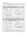
Download 666 KB - ComBlock

Transcript
LOW-POWER PSK MODEM + VITERBI FEC +
TCP SERVER (COM-1704) or
IP ROUTER (COM-1705)
Key Features

Full duplex integrated PSK modem,
including modulation, demodulation,
convolutional error correction, scrambling,
HDLC framing and network interface.

Programmable symbol rates 2.4Ksymbols/s
up to 14 Msymbols/s.

Analog/IF interface:
o
dual I/Q baseband inputs, 1Vpp
differential.
o
70 MHz IF input:
-50 to +5 dBm, 50 Ohm
o
140 MHz IF input:
-50 to +5 dBm, 50 Ohm
Outputs: dual I/Q baseband outputs,
2Vpp differential, 0.5V common
mode.
Convolution error correction, rates 1/2, 2/3,
3/4, 5/6 and 7/8.
Serial HDLC to transmit empty frames over
the synchronous link when no payload data
is available.
V.35 scrambling to randomize the
modulated data stream.
o






Modulation: BPSK/QPSK/OQPSK with
output spectral shaping filter: raised cosine
square root filter with 20% rolloff.

Demodulator acquisition and tracking
threshold: -1 dB Eb/No (2dB Eb/No when
coded with rate ½ FEC).

Built-in test features: BER tester, SNR
measurement, unmodulated carrier


transmitter,
ComScope capture and
display of key internal signals.
Internal TCXO or input for an external,
higher-stability 10 MHz frequency
reference (to be specified at the time of
order)
Supply voltage (to be specified at the time
of order)
o
Direct 3.3V or
o
5V supply with reverse voltage and
overvoltage protection.
Data interface:
o
10/100 Ethernet LAN with built-in
TCP server (COM-1704) or IP
router (COM-1705)
o
USB 2.0
o
Synchronous serial interfaces:
RS-422, LVDS
Small size (3”x3”x0.3”) and low power
(2W)
For the latest data sheet, please refer to the ComBlock
web site: comblock.com/download/com1705.pdf.
These specifications are subject to change without notice.
MSS • 18221-A Flower Hill Way • Gaithersburg, Maryland 20879 • U.S.A.
Telephone: (240) 631-1111 Facsimile: (240) 631-1676 www.ComBlock.com
© MSS 2014
Issued 6/12/2014
For an up-to-date list of ComBlock modules, please
refer to http://www.comblock.com/product_list.html .
Block Diagram
Multiple Outputs
output
selection
IF input
+5 to -50 dBm
VGA
Antialiasing
BPF
16 MHz BW
A/D
converter
Frequency
translation
PSK
demod.
Viterbi
decoder
HDLC
+
Elastic
Buffer
IP Router
RJ-45
10/100/1000Mbps
Synchronous
Serial interface
LVDS
Synchronous
Serial interface
RS422
BER
Measurement
Demodulator
Multiple Inputs
IP router
input
RJ-45
selection
10/100/1000Mbps
Synchronous
Serial interface
LVDS
Synchronous
Serial interface
RS422
Elastic
Buffer
+
HDLC
I
FEC
encoder
PSK
modulator
Interpolation
+ Frequency
translation
Dual
DACs
Internal
Test Sequence
Generator
Modulator
Configuration
An entire ComBlock assembly comprising several ComBlock modules can be monitored and controlled
centrally over a single connection with a host computer. Connection types include built-in types:
 USB
 TCP-IP/LAN,
Other connection types are also available through adjacent ComBlocks.
The module configuration is stored in non-volatile memory.
2
Q
Configuration (Basic)
The easiest way to configure the COM-1704/1705 is to use the ComBlock Control Center software supplied
with the module on CD. In the ComBlock Control Center window detect the ComBlock module(s) by clicking
the
Detect button, next click to highlight the COM-1704/1705 module to be configured, next click the
Settings button to display the Settings window shown below.
3
IMPORTANT NOTE (6/12/14):
Due to limited space within the FPGA, several features are not available in the modem (transmit + receive)
firmware version, but only in the demodulator-only version:
- BER tester
- High-speed USB 2.0 port for modem data transfer
- Comscope.
Demodulator-only firmware will be released shortly.
4
Configuration (Advanced)
1011 = (K = 7, R=1/2, CCSDS)
Alternatively, users can access the full set of
configuration features by specifying 8-bit control
registers as listed below. These control registers can
be set manually through the ComBlock Control
Center “Advanced” configuration or by software
using the ComBlock API (see
www.comblock.com/download/M&C_reference.pdf)
1100 = (K = 7, R=2/3, CCSDS/DVB)
All control registers are read/write.
1101 = (K = 7, R=3/4, CCSDS/DVB)
1110 = (K = 7, R=5/6, CCSDS/DVB)
Differential
Encoding
Definitions for the Control registers are provided
below.
Control Registers
The module configuration parameters are stored in
volatile (SRT command) or non-volatile memory
(SRG command). It is automatically loaded up at
power up. All control registers are read/write.
Transmitter
Parameters
Input
selection /
format, test
modes
Configuration
Select the origin of the transmitter input
data stream.
0 = USB 2.0 (8-bit)
1 = RJ-45 LAN IP (8-bit)
2 = 1-bit synchronous serial LVDS
3 = 1-bit synchronous serial RS-422
4 = internal PRBS-11 test sequence
5 = internal unmodulated carrier
8-bit parallel input bytes are transmitted
MSb first.
REG19(3:0)
Transmit enable digital control on
J4/A17
Typically used to turn on/off an external
power amplifier.
REG19(4)
RX_TXN
Digital control on J4/B17. Typically
used to fast switch a half-duplex external
transceiver between receive and transmit
modes.
REG19(5)
FEC convolutional encoder
Parameters
Configuration
Constraint
0001 = (K = 7, R=1/2, Intelsat)
length K and
0010 = (K = 7, R=2/3, Intelsat)
rate R
0011 = (K = 7, R=3/4, Intelsat)
0100 = (K = 7, R=5/6, Intelsat)
0101 = (K = 7, R=7/8, Intelsat)
TX_ENB
Bypass FEC
encoding
V.35/Intelsat
IESS 308
scrambling
before FEC
encoding
1111 = (K = 7, R=7/8, CCSDS/DVB)
REG12(4:1)
Differential encoding is useful in
removing phase ambiguities at the PSK
demodulator, at the expense of doubling
the bit error rate.
When enabled, the differential decoding
must be enabled at the receiving end.
There is no need to use the differential
encoding to remove phase ambiguities at
the PSK demodulator when the Viterbi
decoder and HDLC decoder are enabled.
0 = disabled
1 = enabled
REG12(5)
0 = encoding enabled
1 = bypass
REG12(6)
0 = enabled
1 = bypass
REG12(7)
HDLC
encoding
0 = enabled
1 = bypass
REG12(0)
PSK Modulator
Parameters
Configuration
Processing
Modulator processing clock. Also serves
clock
as DAC sampling clock.
fclk_tx
20-bit unsigned integer expressed as
fclk_tx* 220 / 234MHz when 26MHz
frequency reference, or
fclk_tx* 220 / 230MHz when 10MHz
frequency reference.
Recommended range: 45-90 MHz
Symbol rate
fsymbol rate tx
REG20 = bits 7-0 (LSB)
REG21 = bits 15 – 8 (MSB)
REG22(3:0) = bits 19 – 16 (MSB)
The modulator symbol rate is in the form
fsymbol rate tx = fclk_tx / 2n
where n ranges from 1 (fclk_tx is twice the
symbol rate) to 15 (symbol rate = fclk_tx /
65536).
5
Modulation
type
Spectrum
inversion
Channel filter
enabled
Transmit sync
word
Signal gain
External
transceiver tx
gain control
Output Center
frequency
(fcout)
n is defined in REG23(3:0)
0 = BPSK
1 = QPSK
2 = OQPSK
REG7(5:0)
Invert Q bit. This is helpful in
compensating any frequency spectrum
inversion occurring in a subsequent RF
frequency translation.
0 = off
1 = on
REG7(6)
0 = enable the spectrum shaping filters
(root raised cosine, interpolation)
1 = bypass the spectrum shaping filters.
(special use in applications when a root
raised cosine filter is not used in the
demodulator.)
REG7(7)
Insert periodic 32 bit synchronization
sequence to assist the demodulator in
synchronizing and recovering
ambiguities. The unique word is 5A 0F
BE 66, transmitted MSb first. 2048 data
symbols are transmitted between
successive unique words. The unique
word is using a simplified BPSK
modulation, irrespective of the
modulation type.
0 = disabled
1 = periodically insert a sync word.
REG19(7)
Signal level.
16-bit unsigned integer.
The maximum level should be adjusted
to prevent saturation. The settings may
vary slightly with the selected symbol
rate. Therefore, we recommend checking
for saturation at the D/A converter when
changing either the symbol rate or the
signal gain.
REG17 = bits 7-0 (LSB)
REG18= bits 15-8 (MSB)
10-bit value for analog gain control
TX_GAIN_CNTRL1 (J4 pin A15)
REG3 = LSB
REG4(1:0) = MSbs
Frequency translation.
32-bit signed integer (2’s complement
representation) expressed as
fcout * 232 / fclk_tx
REG8 = bits 7-0 (LSB)
REG9 = bits 15 – 8
REG10 = bits 23 – 16
REG11 = bits 31 – 23 (MSB)
LSB = Least Significant Byte
MSB = Most Significant Byte
6
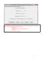
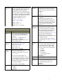
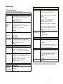
Serial tx bit
rate
Set the nominal input bit rate in order to
supply a regular bit clock to the user data
source. Must be consistent with the
modulator symbol rate, modulation type,
FEC rate, HDLC overhead (when enabled).
When HDLC is disabled, this field MUST
be set to be at least slightly greater than the
transmitter throughput (or else an
underflow condition will occur).
finput bit rate tx * 232 / fclk_rx
REG13 = bits 7-0 (LSB)
REG14 = bits 15 – 8
REG15 = bit 23 – 16
REG16 = bit 31 – 23 (MSB)
Receiver
PSK demodulator
Parameters Configuration
Processing
The demodulator processing clock also
clock
serves as A/D converter sampling clock.
It can be generated within the FPGA or
externally.
Baseline fclk_rx = 80 MSamples/s (for
complex input, 140 MHz IF
undersampling), or 56 MSamples/s (for 70
MHz IF undersampling)
Nominal
The demodulator nominal symbol rate is in
symbol rate
the form fsymbol rate rx * 232 / fclk_rx
fsymbol rate rx
REG25 = bits 7-0 (LSB)
REG26 = bits 15 – 8
REG27 = bit 23 – 16
REG28 = bit 31 – 23 (MSB)
Nominal
Expected center frequency of the received
Center
signal. 32-bit signed integer (2’s
frequency
complement representation) expressed as
(fc_rx)
fc_rx * 232 / fclk_rx.
In the case of IF undersampling, the
residual intermediate frequency is removed
here. For example, in the case of a 70 MHz
IF signal sampled at 56Msamples/s, the 14
MHz residual frequency is removed here
by entering 0xC0000000.
Modulation
type
REG29 (LSB) – REG32 (MSB)
0 = BPSK
1 = QPSK
2 = OQPSK
REG33(5:0)
Spectrum
inversion
Sync word
detection
Frequency
acquisition
range (scan)
AGC
response
time
Rx AGC
enable
Input
selection
Invert Q bit. This is helpful in
compensating any frequency spectrum
inversion occurring during RF frequency
translations.
0 = off
1 = on
REG33(6)
0 = disabled
1 = enabled
Enable when the modulator sends a
periodic synchronization sequence. The
demodulator inherent phase ambiguity can
only be removed if this feature is enabled
at both modulator and demodulator.
REG33(7)
The demodulator natural frequency
acquisition range is around 1% of the
symbol range (depending on modulation,
SNR). The frequency acquisition range can
be extended by frequency scanning.
Scanning steps are spaced (fsymbol rate rx /128)
apart. The user can thus trade-off
acquisition time versus frequency
acquisition range by specifying the number
of scanning steps here.
For example, 16 steps yield a frequency
acquisition range of +/-(fsymbol rate rx *12.5%)
REG24
Users can to optimize the AGC response
time while avoiding instabilities (depends
on external factors such as gain signal
filtering at the RF front-end and symbol
rate). The response time is approximately:
0 = 8 symbols,
1 = 16 symbols,
2 = 32 symbols,
3 = 64 symbols, etc….
10 = every thousand symbols.
Valid range 0 to 14.
REG34(4:0)
REG0 = always 0x05
0 = analog complex (I,Q) input
1 = analog IF input (I-channel ADC)
7 = internal loopback mode, from
modulator.
REG35(2:0)
7
Viterbi FEC decoder
Parameters
Configuration
Constraint length
0001 = (K = 7, R=1/2, Intelsat)
K and rate R
0010 = (K = 7, R=2/3, Intelsat)
0011 = (K = 7, R=3/4, Intelsat)
0100 = (K = 7, R=5/6, Intelsat)
0101 = (K = 7, R=7/8, Intelsat)
1011 = (K = 7, R=1/2, CCSDS)
1100 = (K = 7, R=2/3, CCSDS/DVB)
IP Network
Parameters
IP address
Subnet mask
1101 = (K = 7, R=3/4, CCSDS/DVB)
1110 = (K = 7, R=5/6, CCSDS/DVB)
1111 = (K = 7, R=7/8, CCSDS/DVB)
Differential
Decoding
V.35/Intelsat IESS
308 descrambling
after FEC
decoding
REG37(4:1)
0 = disabled
1 = enabled
REG37(5)
0 = enabled
1 = bypass
REG37(7)
Bypass FEC
decoding
0 = decoding enabled
1 = bypass
REG38(7)
HDLC decoding
0 = enabled
1 = bypass
REG37(0)
0 = USB 2.0 (8-bit)
1 = RJ-45 LAN IP (8-bit)
2 = synchronous serial LVDS
3 = synchronous serial RS-422
4 = BER tester exclusively
REG36(2:0)
Output selection
Gateway IP
address
IP forwarding
Configuration
4-byte IPv4 address.
Example : 0x AC 10 01 80 designates
address 172.16.1.128
The new address becomes effective
immediately (no need to reset the
ComBlock).
REG41 (MSB) - REG44(LSB)
Typically 0x FF FF FF 00
(255.255.255.0)
REG45 (MSB) - REG48(LSB)
(COM-1705 only)
Where to forward IP frames received
over the modem link but not destined to
this LAN.
REG49 (MSB) - REG52 (LSB)
(COM-1705 only)
The IP router can be configured to
forward(1) or not forward (0):
REG53(0): IP multicast frames
REG53(1): IP directed broadcast frames
REG53(2): IP broadcast frames
The recommended setting is zero.
(Re-)Writing to the last control register REG52 is
recommended after a configuration change to enact the
change.
8
Monitoring
Status Registers
Digital status registers are read-only.
PSK/QAM/APSK demodulator monitoring
Parameters
Monitoring
Front-end
12-bit unsigned value controlling the
AGC
internal IF gain and external receiver gain
control RX_AGC1. Inverted scale: 0 is
for the maximum gain.
SREG9 = LSB
SREG10(3:0) = MSbs
Carrier
Residual frequency offset with respect to
frequency
the nominal carrier frequency.
offset
20-bit signed integer (2’s complement)
(fcdelta)
expressed as
fcdelta * 220 / fsymbol rate.
SREG11 = LSB
SREG12
SREG13(3:0) = MSbs
Carrier
Lock is declared if the standard deviation
tracking loop of the phase error is less than 25deg rms.
lock status
0 = unlocked
1 = locked
SREG14 bit 0
Inverse SNR
A measure of noise over signal power.
0 represents a noiseless signal. Valid only
when demodulator is locked.
SREG15
Viterbi FEC decoder monitoring
Parameters
Monitoring
Synchronized
Decoder
built-in BER
(FEC_DEC_LOCK_STATUS variable)
Solid ‘1’ when the Viterbi decoder is
locked. ‘0’ or toggling when unlocked.
SREG14(1)
The Viterbi decoder computes the BER
on the received (encoded) data stream
irrespective of the transmitted bit stream.
Encoded stream bit errors detected over a
1000-bit measurement window.
SREG16 = bits 7 – 0 (LSB)
SREG17 = bits 15 – 8
SREG18 = bits 23 – 16 (MSB)
HDLC decoder monitoring
Parameters
Monitoring
Cumulative
number of
valid bits at
HDLC output
BER measurement
Parameters
Bit Errors
Monitoring
Bit errors can be counted when a PRBS11 test sequence is transmitted.
Number of bit errors in a 1,000,000 bit
window.
32 bit unsigned.
SREG23: error_count[7:0] (LSB)
SREG24: error_count[15:8]
SREG25: error_count[23:16]
SREG26: error_count[31:24] (MSB)
The bit errors counter is updated once
every periodic measurement window.
Reading the value will not reset the
counter.
BER
Synchronization
status
0 = not synchronized. 2047-bit pattern is
not detected.
1 = synchronized
SREG27(0)
IP router monitoring
Parameters
Monitoring
MAC address
Unique 48-bit hardware address (802.3).
In the form SREG30:SREG31:SREG32:
…:SREG35
Parameters
Hardware
self-check
Saturation
Since the MAC address is unique, it can
also be used as a unique identifier in a
radio network with many nodes.
Monitoring
At power-up, the hardware platform
performs a quick self check. The result
is stored in status registers SREG0-7
Properly operating hardware will result
in the following sequence being
displayed:
SREG0/1/2/3/4/5/6/7 = 2C F1 95 xx 0F
01 24 22
Denotes saturation in the transmit path.
SREG8(0)
A dummy read to status register SREG8 is required to
latch multi-byte status fields (to preserve their integrity).
SREG19: LSB
SREG20:
SREG21:
SREG22: MSB
9
Test Points
Test Point
J9
connector
pin A3
J9
connector
pin A4
J9
connector
pin A7
J9
connector
pin A8
J9
connector
pin A15
DONE
Definition
‘1’ when the BER tester is synchronized
with the received PRBS-11 test sequence
‘1’ when BER tester detects a byte error.
Assumes that a PRBS-11 test sequence is
being transmitted. Valid only when the
BER tester is synchronized.
BER measurement: Start of PRBS-11
periodic test sequence detected with less
than 10% bit errors. Periodic pulses every
2047 bits.
Scan frequency (coarse measurement of the
received frequency)
Carrier tracking loop frequency (fine
measurement of the received frequency)
FPGA DONE pin. High indicates proper
FPGA configuration
ComScope Monitoring
Key internal signals can be captured in real-time
and displayed on a host computer using the
ComScope feature of the ComBlock Control
Center. Click on the
button to start, then select
the signal traces and trigger are defined below.
The ComScope feature is only available in the
demod-only firmware options.
Trace 1 signals
Format
Buffer
length
(samples)
512
8-bit
signed
Nominal
sampling
rate
Input
sampling
rate fclk_rx
/R
1 sample /
symbol
1: Input signal (Ichannel) after AGC,
frequency translation,
CIC decimation
8-bit
signed
2: phase after
scanning and before
final carrier tracking
loop
3: Magnitude after
final AGC
4: symbol timing
tracking correction
(accumulated)
8-bit
signed
8-bit
unsigned
1 sample /
symbol
1 sample /
symbol
512
Trace 2 signals
Format
1: Input signal (Qchannel) after AGC,
frequency translation,
CIC decimation
8-bit
signed
Buffer
length
(samples)
512
2: Demodulated I
channel
8-bit
signed
8-bit
signed
Nominal
sampling
rate
Input
sampling
rate fclk_rx
/R
1 sample /
symbol
Input
sampling
rate fclk_rx
Input
sampling
rate fclk_rx
Nominal
sampling
rate
Input
sampling
rate fclk_rx
Variable
Buffer
length
(samples)
512
3: Input signal Ichannel
4: PLL Carrier
tracking phase
correction
(accumulated)
8-bit
signed
Trace 3 signals
Format
1: Input signal Qchannel
8-bit
signed
2: final AGC gain
8-bit
signed
Format
Trigger Signal
N/A
512
512
512
512
512
512
ComScope signals sampling rates can be changed
under software control by adjusting the decimation
10
factor and/or selecting the fclk_rx processing clock as
real-time sampling clock.
In particular, selecting the fclk_rx processing clock as
real-time sampling clock allows one to have the
same time-scale for all signals.
The ComScope user manual is available at
www.comblock.com/download/comscope.pdf.
Output spectrum (after D/A conversion and RF
modulation): 5 Msymbols/s
ComScope Window Sample: showing the received
baseband (I-channel, blue trace) and demodulated
bits (I-channel, center of symbol, red dots)
Output spectrum (after D/A conversion and RF
modulation): 10 Msymbols/s
11
Operation
Filter Response (20% rolloff)
M a g n it u d e (d B )
0
-1 0
-2 0
-3 0
-4 0
-5 0
0 .2
0 .4
0 .6
0 .8
1
1 .2
F re q u e n c y (H z )
1 .4
0 .8
1
1 .2
F re q u e n c y (H z )
1 .4
1 .6
1 .8
x 10
7
P h a s e (d e g re e s )
0
-2 0 0
-4 0 0
-6 0 0
-8 0 0
-1 0 0 0
0
0 .2
0 .4
0 .6
1 .6
1 .8
2
x 10
7
Pseudo-Random Bit Stream (Test
Pattern)
Receiver bandwidth
The receiver bandwidth is as follows:
 Options –A,-D: no anti-aliasing input filter
 Option –B,-E: 60-80 MHz IF input
 Option –C,-F: 130-150 MHz IF input
A periodic pseudo-random sequence can be used as
modulator source instead of the input data stream. A
typical use would be for end-to-end bit-error-rate
measurement of a communication link. The
sequence is 2047-bit long maximum length
sequence generated by a 11-tap linear feedback shift
register:
10
9
8
7
6
5
4
3
2
1
0
A/D sampling rate
The Analog to Digital converter sampling rate fclk_rx
is fixed for a given hardware option.
 Options –A,-D: complex baseband input. 80
MSamples/s
 Option –B,-E: 70 MHz IF input : 56
MSamples/s
 Option –C,-F: 140 MHz IF input: 80
MSamples/s
XNOR
Pseudo-Random
Sequence
The first 100 bits of the PN sequence are as follows:
0000000000 0111111111 0011111110 0001111100
1100111000 0000010011 1111010001 1110110100
1101001100 0011000001
Demodulator frequency acquisition
The center frequency acquisition window is
programmable. The natural acquisition window is
1% of the symbol rate. This window can be
extended through frequency scanning, at the
expense of a longer acquisition time.
Filter Response
This module is configured with a 20% rolloff filter.
12
Interfaces
1-bit synchronous serial
Clock synchronous 1-bit serial interfaces are available at the modulator data input and demodulator data output
as LVDS or RS-422 electrical signals. The timing diagram is show below:
Receiver Interface
SERIAL_RX_CLK_OUT
SERIAL_RX_DATA_OUT
rising edge is the best time
for user to read the rx data bit
Transmitter Interface
SERIAL_TX_CLK_OUT
SERIAL_TX_DATA_IN
falling edge is the best time
for user to send a tx data bit
130018
The modem provides the transmit and receive clocks to the user. When HDLC encoding is enabled, the user can
decide not to transmit any data by setting the SERIAL_TX_DATA_VALID_IN signal to ‘0’. When the user
supplies no data, the modem will send empty HDLC frames over the synchronous modulated link. When HDLC
encoding is disabled, the user must supply a new data bit before every SERIAL_TX_CLK_OUT rising edge.
IP Routing (COM-1705)
The reverse process is performed at the receiving
end. Erroneous packets which do not pass the CRC
test are rejected.
The forwarding rules are specified in the RFC1812
document “Requirements for IP Version 4 Routers”.
When an IP packet is received over the modulated
link interface, the IP router will check whether the
packet destination is for this local subnet or not. If
not, the packet will be forwarded to the default
gateway IP. To determine whether a packet is
destined to this subnet, the router compares the
masked destination address (Destination IP address
& subnet mask) with the masked router address
(IP router own IP address & subnet mask).
Concept: On the transmit side, IP packets from the
RJ-45 LAN interface are forwarded to the
modulated link if the IP destination address is
deemed remote.
The IP packets received over the LAN are stripped
of their link layer information: Ethernet source
address, destination address and type are removed,
keeping only the IP fields.
TCP, UDP, ICMP and IGMP packets are processed
since they are transmitted as IP datagrams.
Non IP packets are rejected.
IP packets whose Time-To-Live field has reached
zero are discarded. For the other packets, the TTL is
decremented.
Limited broadcasts (those with destination IP
address 255.255.255.255) are not forwarded.
Example:
 Router IP address: 172.16.1.1
 Router subnet mask: 255.255.255.0
 Packet destination IP address is 74.54.97.66
Masked packet destination: 74.54.97.0
Masked router address: 172.16.1.0
Since the masked packet destination does not match
the masked router address, the packet is not for a
local destination. Consequently the router will
forward the packet to the default gateway.
Valid IP packets are re-encapsulated inside an
Ethernet packet, one IP packet per Ethernet packet.
The IP to Ethernet MAC address association is
determined by means of an Address Resolution
Protocol (ARP) query-reply transaction. The COM1705 will send an ARP request asking “whois the
destination IP address?” and will wait for the ARP
reply with the MAC information.
Packets received while the IP router is busy are also
discarded without notification.
The IP packet maximum size (maximum
transmission unit (MTU)) is 1500 bytes. No
datagram fragmentation is necessary nor used.
The IP packets are then encapsulated within a bitwise HDLC frame, one packet per frame. A 16-bit
CRC is inserted at the end of each frame to detect
errors upon reception.
14
TCP Server (COM-1704)
Concept: This module acts as a TCP server (socket),
waiting for a remote TCP client to initiate a
connection on port 1028. Once the TCP connection
is established, the remote TCP client can write and
read data to/from the modem over the network.
Mechanical Interface
Mounting hole
(2.840", 2.840")
Mounting hole
(0.160", 2.840")
POWER
(+5VDC or +3.3VDC)
TERMINAL BLOCK
The TCP protocol includes a flow-control
mechanism. Therefore, it is impossible for a TCP
client to overflow the transmitter. After writing a
buffer to the TCP socket, the client application must
check how many bytes were actually sent.
RJ45
LAN
J2
J1
A1
A20 B20
Underflow is not possible either because the COM1704 transmitter sends empty HDLC frames over
the link when there is not enough payload data to
fill the link.
A20 pin
(0.100", 2.250")
Analog I/O
2 rows x 20 pins
2mm pitch
female right angle
connector
Digital interface
98-pin card-edge
(PCIe type)
COM-1700
J9
TOP VIEW
USB
A USB port is available for monitoring and control
purposes only. It cannot be used for transferring
payload data.
Corner
(3.330",2.510")
USB DATA
port. MiniAB
RS-422 (4/4)
J3
Corner
(3.000",3.000")
EXT-REF
UMCC
A1 B1
IFin
UMCC
J5
A49
card-edge
to ARM JTAG
J7
USB DEV port.
MiniAB
Mounting hole
(0.160", 0.160")
FPGA JTAG
Mounting hole
(2.840", 0.160")
Corner
(3.330", 0.490")
Corner(0.000", 0.000")
Mounting hole diameter: 0.125"
Use 5/8" spacers between two stacked boards
Board thickness 0.062"
120012
Schematics
The board schematics are available on-line at
http://comblock.com/download/com_1700schematics.pdf
15
Multiple FPGA
configurations
+ user data
USB Hub / PC USB Hub / PC
Developer port High-speed
USB
connector
USB
connector
32-bit
ARM
Micro.
120 MHz
USB 2.0
PHY
1Gb NAND
Flash
RS-422
drivers
(4/4)
header
LAN switch /
PC port
RJ45 LAN
connector
Signal
Power
10/100/1000
Ethernet PHY
LVTTL
or
98-pin LVDS
FPGA
Xilinx
XC6SLX45-L1
TCXO
Electrical Interfaces
PCIe
card
edge
10/100 Ethernet LAN
for data, monitoring
and control
USB monitoring and
control
IF input
UMCC external
frequency
reference
2*12-bit
DACs
2*10-bit
ADCs
Modulated baseband
outputs
40-pin 2mm connector
120010
COM-1704/1705 (Options –A/D)
Hardware Block Diagram
Multiple FPGA
configurations
+ user data
USB Hub / PC USB Hub / PC
Developer port High-speed
USB
connector
USB
connector
32-bit
ARM
Micro.
120 MHz
USB 2.0
PHY
1Gb NAND
Flash
header
RS-422
drivers
(4/4)
TCXO
UMCC external
frequency
reference
LAN switch /
PC port
RJ45 LAN
connector
10/100/1000
Ethernet PHY
LVTTL
or
98-pin LVDS
FPGA
Xilinx
XC6SLX45-L1
2*12-bit
DACs
External 10 MHz
frequency reference
PCIe
card
edge
Synchronous serial,
LVDS
Synchronous serial,
RS-422
Connector
Right-angle 3.81mm terminal
block.
3.1 – 3.5V DC regulated or
4.75 – 5.25V DC unregulated
(select at the time of order)
2W typ.
RJ45
Supports auto MDIX to alleviate
the need for crossover cable.
Mini-USB connector
Type AB
Full speed / Low Speed
70 MHz center frequency
-50 to +5 dBm
AC coupled.
50 Ohm
UMCC female connector J6
2Vpp differential (1Vpp single
ended), 0.5Vcommon-mode
voltage.
Because of the high source
impedance (1KOhm), these
signals should ‘see’ a high input
impedance.
40-pin 2mm connector J4
Hardware options –D,E,F.
External 10 MHz frequency
reference for frequency
synthesis.
Sinewave, clipped sinewave or
squarewave.
UMCC female connector (J5).
Input is AC coupled.
Minimum level 0.6Vpp.
Maximum level: 3.3Vpp.
98-pin card edge, PCIe., J9
16-pin header J1
Pinout
10-bit
ADC
LAN Connector RJ1
Band-Pass
Filter
VGA
UMCC
IF IN
40-pin 2mm connector
120011
COM-1704/1705 (Options –B/C/E/F)
Hardware Block Diagram
The RJ45 Jack is wired as a standard PC network
interface card. As the Ethernet PHY supports autoMDIX, there is no need for special crossover cables
when connecting directly to a PC. The LAN speed
is limited to 10/100 Mbps to minimize power
consumption without restricting operation.
16
RJ-45 Jack
USB
Two USB ports labeled USB DATA and J7 are
equipped with a mini type AB connectors.
(G = GND). The COM-1704/1705 acts as a USB
device.
ID
G
5
D+
4
1 Tx+
2 Tx3 Rx+
6 Rx-
D-
2
5V
3
8
1
1
Right Connector J9
Top
Bottom
A1 B1
LVDS_RX_CLK_OUTLVDS_RX_CLK_OUT+
LVDS_SERIAL_RX_DATA_OUTLVDS_SERIAL_RX_DATA_OUT+
LVDS_SERIAL_TX_CLK_OUTLVDS_SERIAL_TX_CLK_OUT+
LVDS_SERIAL_TX_DATA_INLVDS_SERIAL_TX_DATA_IN+
LVDS_SERIAL_TX_DATA_VALID_INLVDS_SERIAL_TX_DATA_VALID_IN+
GND
GND
GND
M&C_TX
M&C_RX
A49 B49 130017
17
Analog I/O Connector J4
B1
A1
Configuration Management
GND
RX_I_P
GND
RX_Q_P
GND
RX_AGC1
GND
This specification document is consistent with the
following software versions:
 COM-1704/1705 FPGA firmware: Version
3 and above.
 ComBlock Control Center graphical user
interface: Revision 3.08p and above.
GND
RX_I_N
GND
RX_Q_N
GND
GND
RX_AGC2
GND
TX_I_P
GND
TX_Q_P
GND
TX_GAIN_CNTRL1
GND
TX_I_N
GND
TX_Q_N
GND
GND
TX_ENB
M&C TX
RX_TXN
M&C RX
ComBlock Ordering Information
COM-1704
LOW-POWER PSK MODEM + VITERBI FEC +
TCP SERVER
GND
A20
B20
RS-422 Connector J1
1
RS422_SERIAL_TX_CLK_OUT+
RS422_SERIAL_RX_CLK_OUT+
RS422_SERIAL_RX_DATA_OUT+
RS422_SERIAL_TX_DATA_IN+
RS422_SERIAL_TX_DATA_VALID_IN+
2
COM-1705
LOW-POWER PSK MODEM + VITERBI FEC +
IP ROUTER
Options (select at the time of order):
-A (baseband input, TCXO),
-B (70 MHz IF input, TCXO)
-C (140 MHz IF input, TCXO)
RS422_SERIAL_TX_DATA_IN-D (baseband input, 10 MHz external clock),
RS422_SERIAL_TX_DATA_VALID_IN-E (70 MHz IF input, 10 MHz external clock),
-F (140 MHz IF input, 10 MHz external clock)
RS422_SERIAL_TX_CLK_OUTRS422_SERIAL_RX_CLK_OUTRS422_SERIAL_RX_DATA_OUT-
130016
I/O Compatibility List
(not an exhaustive list)
Baseband Interface
COM-1500 FPGA/ARM development platform
Analog Interface
COM-3501 UHF transceiver
COM-3505 2.4/5 GHz transceiver
COM-3506 [400MHz – 3GHz] RF transceiver
COM-4001/2/3/5/6 RF Quadrature Modulators (requires
a simple harness: electrically compatible interface but not
mechanically plug-in compatible)
Please also specify +5V unregulated or +3.3V
regulated supply voltage.
MSS • 18221-A Flower Hill Way •
Gaithersburg, Maryland 20879 • U.S.A.
Telephone: (240) 631-1111
Facsimile: (240) 631-1676
E-mail: [email protected]
COM-4410 [70 MHz – 2.2 GHz] quadrature RF
modulator
18