1
SAFETY PRECAUTIONS
(Read these precautions before using this product.)
Before using the product, please read this manual and the relevant manuals carefully and pay full attention
to safety to handle the product correctly.
In this manual, the safety precautions are classified into two levels: "
WARNING" and "
CAUTION".
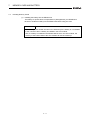
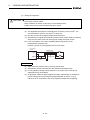
WARNING
Indicates that incorrect handling may cause hazardous conditions,
resulting in death or severe injury.
CAUTION
Indicates that incorrect handling may cause hazardous conditions,
resulting in minor or moderate injury or property damage.
Under some circumstances, failure to observe the precautions given under "
CAUTION" may lead to
serious consequences.
Observe the precautions of both levels because they are important for personal and system safety.
Make sure that the end users read this manual and then keep the manual in a safe place for future
reference.
[DESIGN PRECAUTIONS]
WARNING
Configure safety circuits external to the programmable controller to ensure that the entire system
operates safely even when a fault occurs in the external power supply or the programmable
controller. Failure to do so may result in an accident due to an incorrect output or malfunction.
(1) Configure external safety circuits, such as an emergency stop circuit, protection circuit, and
protective interlock circuit for forward/reverse operation or upper/lower limit positioning.
(2) When the programmable controller detects the following error conditions, it stops the operation
and turn off all the outputs.
• Overcurrent or overvoltage protection of the power supply module is activated.
• The CPU module detects an error such as a watchdog timer error by the self-diagnostic
function.
All outputs may turn on when an error occurs in the part, such as I/O control part, where the
CPU module cannot detect any error. To ensure safety operation in such a case, provide a
safety mechanism or a fail-safe circuit external to the programmable controller. For a fail-safe
circuit example, refer to Chapter 9 LOADING AND INSTALLATION in this manual.
(3) Outputs may remain on or off due to a failure of an output module relay or transistor. Configure
an external circuit for monitoring output signals that could cause a serious accident.
In an output module, when a load current exceeding the rated current or an overcurrent caused by a
load short-circuit flows for a long time, it may cause smoke and fire. To prevent this, configure an
external safety circuit, such as a fuse.
A-1
[DESIGN PRECAUTIONS]
WARNING
Configure a circuit so that the programmable controller is turned on first and then the external power
supply. If the external power supply is turned on first, an accident may occur due to an incorrect
output or malfunction.
For the operating status of each station after a communication failure, refer to relevant manuals for
the network.
Incorrect output or malfunction due to a communication failure may result in an accident.
When controlling a running programmable controller from a peripheral connected to the CPU module
or from a personal computer connected to a special function module, configure an interlock circuit in
the sequence program to ensure that the entire system will always operate safely.
For program modification and operating status change, read relevant manuals carefully and ensure
the safety before operation.
Especially, in the case of a control from an external device to a remote programmable controller,
immediate action cannot be taken for a problem on the programmable controller due to a
communication failure.
To prevent this, configure an interlock circuit in the sequence program , and determine corrective
actions to be taken between the external device and CPU module in case of a communication
failure.
When setting up the system, do not allow any empty slot on the base unit.
If any slot is left empty, be sure to use a blank cover (A1SG60) or a dummy module (A1SG62) for it.
Otherwise, internal parts of the module may be flied in the short circuit test or when an overcurrent or
overvoltage is accidentally applied to the external I/O section.
CAUTION
Do not install the control lines or communication cables together with the main circuit lines or power
cables.
Keep a distance of 100mm (3.94inches) or more between them.
Failure to do so may result in malfunction due to noise.
When a device such as a lamp, heater, or solenoid valve is controlled through an output module, a
large current (approximately ten times greater than normal) may flow when the output is turned from
off to on.
Take measures such as replacing the module with one having a sufficient current rating.
Time from when the CPU module is powered on or is reset to when it enters in RUN status depends
on the system configuration, parameter settings, and program size.
Design the program so that the entire system will always operate safely, regardless of the time.
A-2
[INSTALLATION PRECAUTIONS]
CAUTION
Use the programmable controller under the environment that meets the general specifications in this
manual.
Failure to do so may result in electric shock, fire, malfunction, or damage to or deterioration of the
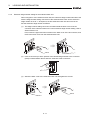
product.
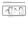
To mount the CPU module, while pressing the module mounting lever located in the lower part of the
module, fully insert the module fixing projection(s) into the hole(s) in the base unit and press the
module until it snaps into place.
Incorrect mounting may cause malfunction, failure or a drop of the module.
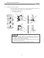
When using the programmable controller in an environment of frequent vibrations, fix the module
with the screw.
Tighten the screw within the specified torque range.
Undertightening can cause drop of the screw, short circuit or malfunction.
Overtightening can damage the screw and/or module, resulting in drop, short circuit, or malfunction.
Insert securely the module fixing projection at the bottom of the AnS series module into the fixing
hole in the base unit and then tighten the module fixing screw within the specified torque.
When no screw is tightened, even if the module is installed correctly, it may cause malfunctions, a
failure or a drop of the module.
Tightening the screw excessively may damage the screw and/or the module, resulting in a drop of
the module, a short circuit or malfunctions.
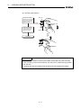
When using an extension cable, connect it to the extension cable connector of the base unit
securely.
Check the connection for looseness.
Poor contact may cause incorrect input or output.
When using a memory card, fully insert it into the memory card slot.
Check for incomplete connection after installing it.
Poor electrical contact may cause malfunctions.
Shut off the external power supply for the system in all phases before mounting or removing the
module.
Failure to do so may result in damage to the product.
Do not directly touch any conductive part of the module.
Doing so can cause malfunction or a failure of the module.
A-3
[WIRING PRECAUTIONS]
WARNING
Shut off the external power supply for the system in all phases before wiring.
Failure to do so may result in electric shock or damage to the product.
After wiring, attach the included terminal cover to the module before turning it on for operation.
Failure to do so may result in electric shock.
A-4
[WIRING PRECAUTIONS]
CAUTION
Ground the FG and LG terminals to the protective ground conductor dedicated to the programmable
controller.
Failure to do so may result in electric shock or malfunction.
Use applicable solderless terminals and tighten them within the specified torque range. If any spade
solderless terminal is used, it may be disconnected when the terminal screw comes loose, resulting
in failure.
Check the rated voltage and terminal layout before wiring to the module, and connect the cables
correctly.
Connecting a power supply with a different voltage rating or incorrect wiring may cause a fire or
failure.
Do not connect multiple power supply modules to one module in parallel.
The power supply modules may be heated, resulting in a fire or failure.
Connectors for external connection must be crimped or pressed with the tool specified by the
manufacturer, or must be correctly soldered.
Incomplete connections could result in short circuit, fire or malfunction.
Tighten the terminal screw within the specified torque range.
Undertightening can cause short circuit, fire, or malfunction.
Overtightening can damage the screw and/or module, resulting in drop, short circuit, or malfunction.
Prevent foreign matter such as dust or wire chips from entering the module.
Such foreign matter can cause a fire, failure or malfunction.
A protective film is attached to the top of the CPU module to prevent foreign matter, such as wire
chips, from entering during wiring.
Do not remove the film during wiring.
Remove it for heat dissipation before system operation.
Mitsubishi programmable controllers must be installed in control panels.
Connect the main power supply to the power supply module in the control panel through a relay
terminal block.
Wiring and replacement of a power supply module must be performed by maintenance personnel
who is familiar with protection against electric shock. (For the wiring methods, refer to Section 9.5.)
A-5
[STARTUP AND MAINTENANCE PRECAUTIONS]
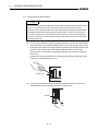
WARNING
Do not touch any terminal while power is on.
Doing so will cause electric shock.
Correctly connect the battery connector.
Do not charge, disassemble, heat, short-circuit, solder, or throw the battery into the fire.
Doing so will cause the battery to produce heat, explode, or ignite, resulting in injury and fire.
Shut off the external power supply for the system in all phases before cleaning the module or
retightening the terminal screws or module fixing screws.
Failure to do so may result in electric shock.
Undertightening the terminal screws can cause short circuit or malfunction.
Overtightening can damage the screw and/or module, resulting in drop, short circuit, or malfunction.
CAUTION
Before performing online operations (especially, program modification, forced output and operation
status change) for the running CPU module from the peripheral connected, read relevant manuals
carefully and ensure the safety.
Improper operation may damage machines or cause accidents.
Do not disassemble or modify the modules.
Doing so may cause failure, malfunction, injury, or a fire.
Use any radio communication device such as a cellular phone or PHS (Personal Handy-phone
System) more than 25cm (9.84inches) away in all directions from the programmable controller.
Failure to do so may cause malfunction.
Shut off the external power supply for the system in all phases before mounting or removing the
module. Failure to do so may cause the module to fail or malfunction.
After the first use of the product, do not mount/remove the module to/from the base unit, and the
terminal block to/from the module more than 50 times (IEC 61131-2 compliant) respectively.
Exceeding the limit of 50 times may cause malfunction.
Do not drop or apply any shock to the battery to be installed in the module.
Doing so may damage the battery, causing the battery fluid to leak inside the battery. If the battery is
dropped or any shock is applied to it, dispose of it without using.
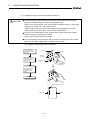
Before handling the module, touch a grounded metal object to discharge the static electricity from
the human body.
Failure to do so may cause the module to fail or malfunction.
A-6
[DISPOSAL PRECAUTIONS]
CAUTION
When disposing of the product, treat it as an industrial waste.
When disposing of batteries, separate them from other wastes according to the local regulations.
(For details of the Battery Directive in EU member states, refer to Appendix 7.)
[TRANSPORTATION PRECAUTIONS]
CAUTION
When transporting lithium batteries, follow the transportation regulations. (For details of the
regulated models, refer to Appendix 6.)
A-7
CONDITIONS OF USE FOR THE PRODUCT
(1) Mitsubishi programmable controller ("the PRODUCT") shall be used in conditions;
i) where any problem, fault or failure occurring in the PRODUCT, if any, shall not lead to any major
or serious accident; and
ii) where the backup and fail-safe function are systematically or automatically provided outside of
the PRODUCT for the case of any problem, fault or failure occurring in the PRODUCT.
(2) The PRODUCT has been designed and manufactured for the purpose of being used in general
industries.
MITSUBISHI SHALL HAVE NO RESPONSIBILITY OR LIABILITY (INCLUDING, BUT NOT
LIMITED TO ANY AND ALL RESPONSIBILITY OR LIABILITY BASED ON CONTRACT,
WARRANTY, TORT, PRODUCT LIABILITY) FOR ANY INJURY OR DEATH TO PERSONS OR
LOSS OR DAMAGE TO PROPERTY CAUSED BY the PRODUCT THAT ARE OPERATED OR
USED IN APPLICATION NOT INTENDED OR EXCLUDED BY INSTRUCTIONS, PRECAUTIONS,
OR WARNING CONTAINED IN MITSUBISHI'S USER, INSTRUCTION AND/OR SAFETY
MANUALS, TECHNICAL BULLETINS AND GUIDELINES FOR the PRODUCT.
("Prohibited Application")
Prohibited Applications include, but not limited to, the use of the PRODUCT in;
• Nuclear Power Plants and any other power plants operated by Power companies, and/or any
other cases in which the public could be affected if any problem or fault occurs in the PRODUCT.
• Railway companies or Public service purposes, and/or any other cases in which establishment of
a special quality assurance system is required by the Purchaser or End User.
• Aircraft or Aerospace, Medical applications, Train equipment, transport equipment such as
Elevator and Escalator, Incineration and Fuel devices, Vehicles, Manned transportation,
Equipment for Recreation and Amusement, and Safety devices, handling of Nuclear or
Hazardous Materials or Chemicals, Mining and Drilling, and/or other applications where there is a
significant risk of injury to the public or property.
Notwithstanding the above, restrictions Mitsubishi may in its sole discretion, authorize use of the
PRODUCT in one or more of the Prohibited Applications, provided that the usage of the PRODUCT
is limited only for the specific applications agreed to by Mitsubishi and provided further that no
special quality assurance or fail-safe, redundant or other safety features which exceed the general
specifications of the PRODUCTs are required. For details, please contact the Mitsubishi
representative in your region.
A-8
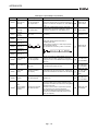
REVISIONS
The manual number is given on the bottom left of the back cover.
Print Date
*Manual Number
Revision
Dec., 1999
SH (NA) 080065-A
First printing
Mar., 2000
SH (NA) 080065-B
Addition of model
Dec., 2003
SH (NA) 080065-C
QA1S33B
Addition of model
A1SY42P
Partial correction
About Manual, Section 2.2.1, 2.3, 3.1, 4.1.3, 6.1, 6.3, 7.2, 8.1.3, 9.1.2, 9.1.4,
9.1.5, 9.1.6, 9.2, 9.6, 11.3, 11.4.1, Appendix 2.1, 2.3, 4, 5.3
Addition
Appendix 6
Delete
Appendix 5 List of Instruction Processing Time
Oct., 2006
SH (NA) 080065-D
Partial correction
SAFETY PRECAUTIONS, Section 1.1, 2.2.1, 2.2.3, 2.3, Chapter 3, Section 3.1,
4.1, 4.1.1, 4.1.3, 4.1.4, 4.2.1, 4.2.2, 4.2.3, 4.2.6, 4.3, 4.4.1, 4.5, 4.6.1, 4.6.3, 5.1,
5.2, 6.1.1, 6.2, 7.2.1, 7.3, 7.7, 7.7.1, 7.7.2, Chapter 8, Section 8.1.3, 8.2.4, 8.2.6,
9.1.1, 9.1.2, 9.1.3, 9.1.4, 9.2, 9.2.4, 9.5, 9.5.1, 9.5.2, 10.3, 10.4, 11.2.8, 11.3.2,
11.4.1, Appendix 2.1, 2.3, 4.1, WARRANTY
Addition
Section 9.5.1, 9.5.2, 11.2.10
May, 2007
SH (NA) 080065-E
Partial correction
Section 2.3, 8.1.3, 8.2.7, 9.5.1, 9.5.2, 11.4.2
Addition
Section 8.1.7
Oct., 2008
SH (NA) 080065-F
Partial correction
SAFETY PRECAUTIONS, Chapter 3, Section 4.2.2, 5.1, 7.2.1, 7.7, 9.5.1, 11.4.1
Addition
Appendix 7, 7.1, 7.2
Mar., 2010
SH (NA) 080065-G
Partial correction
"PLC" was changed to "programmable controller".
SAFETY PRECAUTIONS, Section 2.2.1, 2.3, 4.1, 4.2.6, 4.4.3, 4.6.1, 5.1, 7.6,
7.7.2, Chapter 8, Section 9.1.2, 9.2, 9.5.1, 11.3.2, 11.4.1, Appendix 2.1, 2.2, 4.1,
5.1, 6.1, WARRANTY
Addition
CONDITIONS OF USE FOR THE PRODUCT
Japanese Manual Version SH-080066-H
This manual confers no industrial property rights or any rights of any other kind, nor dose it confer any patent licenses.
Mitsubishi Electric Corporation cannot be held responsible for any problems involving industrial property rights which may
occur as a result of using the contents noted in this manual.
1999 MITSUBISHI ELECTRIC CORPORATION
A-9
Introduction
Thank you for purchasing the Mitsubishi programmable controller MELSEC-Q series.
Before using your new programmable controller, please read this manual thoroughly to gain an
understanding of its functions so you can use it properly.
Please forward a copy of this manual to the end user.
Table of Contents
1
1.1
OVERVIEW
1 - 1 to 1 - 2
Features ........................................................................................................................................1 - 2
2
SYSTEM CONFIGURATION
2 - 1 to 2 - 23
2.1
System Configuration ....................................................................................................................2 - 1
2.2
Precautions When Configuring the System...................................................................................2 - 2
2.2.1
Hardware...............................................................................................................................2 - 2
2.2.2
Software package .................................................................................................................2 - 4
2.2.3
Precautions when using GPP function software packages and A8PUE peripheral devices which
are not compatible with AnU .................................................................................................2 - 7
2.3
System Equipment ........................................................................................................................2 - 8
2.4
System Configuration Overview ..................................................................................................2 - 22
2.4.1
QCPU-A system..................................................................................................................2 - 23
3
SPECIFICATIONS
4
CPU MODULE
4.1
4.2
3 - 1 to 3 - 1
4 - 1 to 4 - 46
Performance Specifications...........................................................................................................4 - 1
4.1.1
Overview of operation processing.........................................................................................4 - 4
4.1.2
Operation processing of RUN, STOP, PAUSE, and STEP-RUN..........................................4 - 7
4.1.3
Operation processing upon instantaneous power failure ......................................................4 - 9
4.1.4
Self-diagnostics functions ...................................................................................................4 - 10
4.1.5
Device list............................................................................................................................4 - 13
Parameter Setting Ranges ..........................................................................................................4 - 15
4.2.1
List of parameter setting range ...........................................................................................4 - 15
4.2.2
Memory capacity setting (for main program, file register, comment, etc.) ..........................4 - 18
4.2.3
Setting ranges of timer and counter ....................................................................................4 - 22
4.2.4
I/O devices ..........................................................................................................................4 - 24
4.2.5
I/O assignment of special function module .........................................................................4 - 25
4.2.6
MELSECNET/MINI-S3 auto refresh processing .................................................................4 - 26
4.3
Function List ................................................................................................................................4 - 31
4.4
Functions added to QCPU-A.......................................................................................................4 - 33
4.4.1
Boot operation from built-in ROM........................................................................................4 - 33
4.4.2
Usage of 1ms timer .............................................................................................................4 - 36
4.4.3
Sequence accumulation time processing............................................................................4 - 39
4.5
Handling Precautions ..................................................................................................................4 - 41
4.6
Part Names and Settings ............................................................................................................4 - 43
A - 10
4.6.1
Part names..........................................................................................................................4 - 43
4.6.2
Switch operation after program write ..................................................................................4 - 46
4.6.3
Latch clear operation...........................................................................................................4 - 46
4.6.4
Handling of the memory card at power-on ..........................................................................4 - 46
5
POWER SUPPLY MODULE
5 - 1 to 5 - 4
5.1
Specifications ................................................................................................................................5 - 1
5.2
Part Names ...................................................................................................................................5 - 3
6
6.1
BASE UNIT AND EXTENSION CABLE
6 - 1 to 6 - 5
Specifications ................................................................................................................................6 - 1
6.1.1
Base unit specifications.........................................................................................................6 - 1
6.1.2
Extension cables specifications ............................................................................................6 - 2
6.2
Part Names and Settings ..............................................................................................................6 - 3
6.3
Setting the Extension Stage Numbers ..........................................................................................6 - 5
7
7.1
MEMORY CARD AND BATTERY
Memory Card.................................................................................................................................7 - 1
7.1.1
7.2
7 - 1 to 7 - 13
Specifications ........................................................................................................................7 - 1
Battery Specifications (CPU Module and Memory Card Batteries) ...............................................7 - 2
7.2.1
Specifications ........................................................................................................................7 - 2
7.2.2
Handling precautions ............................................................................................................7 - 3
7.3
Handling Memory Cards................................................................................................................7 - 4
7.4
Part Names of Memory Card.........................................................................................................7 - 5
7.5
Installing/Removing a Memory Card .............................................................................................7 - 6
7.6
Installing Batteries (CPU Module and Memory Card Batteries) ....................................................7 - 7
7.7
Battery Replacement.....................................................................................................................7 - 8
7.7.1
Battery life .............................................................................................................................7 - 9
7.7.2
Battery replacement procedure...........................................................................................7 - 11
8
8.1
8.2
EMC AND LOW VOLTAGE DIRECTIVES
8 - 1 to 8 - 13
Requirements for Compliance with EMC Directive .......................................................................8 - 1
8.1.1
EMC standards .....................................................................................................................8 - 1
8.1.2
Installation inside the control panel .......................................................................................8 - 2
8.1.3
Cable.....................................................................................................................................8 - 3
8.1.4
Power supply module............................................................................................................8 - 8
8.1.5
Ferrite core............................................................................................................................8 - 8
8.1.6
Noise filter (power supply line filter) ......................................................................................8 - 9
8.1.7
Power line for external power supply terminal ......................................................................8 - 9
Requirements for Compliance with Low Voltage Directive..........................................................8 - 10
8.2.1
Standard applied for MELSEC-AnS series programmable controller .................................8 - 10
8.2.2
Precautions when using the MELSEC-AnS series programmable controller......................8 - 10
8.2.3
Supply power ......................................................................................................................8 - 11
8.2.4
Control panel.......................................................................................................................8 - 12
8.2.5
Module installation ..............................................................................................................8 - 13
8.2.6
Ground ................................................................................................................................8 - 13
A - 11
8.2.7
9
9.1
External wiring.....................................................................................................................8 - 13
LOADING AND INSTALLATION
9 - 1 to 9 - 29
Module Installation ........................................................................................................................9 - 1
9.1.1
Handling precautions ............................................................................................................9 - 1
9.1.2
Precautions on base unit installation.....................................................................................9 - 2
9.1.3
Installation and removal of the dustproof cover ....................................................................9 - 5
9.1.4
Installation and removal of modules......................................................................................9 - 7
9.1.5
Extension stage number setting for the extension base unit...............................................9 - 11
9.1.6
Connecting/disconnecting the extension cable ...................................................................9 - 12
9.2
Concept of Fail Safe Circuit.........................................................................................................9 - 15
9.3
Installation Environment ..............................................................................................................9 - 20
9.4
Calculation Method of Heat Amount Generated by the Programmable Controller......................9 - 21
9.5
9.6
10
Wiring ..........................................................................................................................................9 - 23
9.5.1
Wiring precautions ..............................................................................................................9 - 23
9.5.2
Wiring to module terminals..................................................................................................9 - 28
Precautions when Connecting the Uninterruptible Power Supply (UPS) ....................................9 - 29
MAINTENANCE AND INSPECTION
10 - 1 to 10 - 5
10.1 Daily Inspection ...........................................................................................................................10 - 2
10.2 Periodic Inspection ......................................................................................................................10 - 3
10.3 When Reoperating a Programmable Controller After Storing it with a Battery Unconnected .....10 - 4
10.4 When a Programmable Controller is Reoperated After Stored with the Battery Over the Battery Life
....................................................................................................................................................10 - 5
11
TROUBLESHOOTING
11 - 1 to 11 - 27
11.1 Fundamentals of Troubleshooting...............................................................................................11 - 1
11.2 Troubleshooting...........................................................................................................................11 - 2
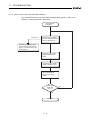
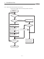
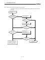
11.2.1 Troubleshooting flowchart ...................................................................................................11 - 2
11.2.2 Flow for actions when the POWER LED is turned off .........................................................11 - 3
11.2.3 Flow for actions when the MODE LED turns off..................................................................11 - 4
11.2.4 Flow for actions when the RUN LED is turned off...............................................................11 - 5
11.2.5 Flow for actions when the RUN LED is flashing..................................................................11 - 6
11.2.6 Flow for actions when the ERR. LED is turned on ..............................................................11 - 7
11.2.7 Flow for actions when the ERR. LED is flashing.................................................................11 - 8
11.2.8 Flow for actions when the output module's output load does not turn on ...........................11 - 9
11.2.9 Flow for actions when the program cannot be written.......................................................11 - 10
11.2.10 Flow for actions when the CPU module is not started up ................................................11 - 11
11.3 Error Code List ..........................................................................................................................11 - 12
11.3.1 Procedure to read an error code .......................................................................................11 - 12
11.3.2 Error code list for the QCPU-A (A Mode) ..........................................................................11 - 13
11.4 Fault Examples with I/O Modules..............................................................................................11 - 22
11.4.1 Faults with the input circuit and the corrective actions......................................................11 - 22
11.4.2 Faults in the output circuit .................................................................................................11 - 24
A - 12
APPENDICES
Appendix 1
Instruction List .............................................................................................................. App - 1
Appendix 1.1
Appendix 2
Appendix - 1 to Appendix - 62
Precautions for write during RUN of a dedicated instruction ............................ App - 14
Lists of Special Relays and Special Registers .......................................................... App - 15
Appendix 2.1
Special relays................................................................................................... App - 15
Appendix 2.2
Special Registers ............................................................................................. App - 27
Appendix 3
Peripheral Device....................................................................................................... App - 46
Appendix 4
Precautions for Utilizing the Existing Sequence Programs for the QCPU-A.............. App - 48
Appendix 4.1
Instructions with different specifications............................................................ App - 49
Appendix 4.2
Special relays and special registers with different specifications...................... App - 50
Appendix 4.3
Parameter setting.............................................................................................. App - 51
Appendix 4.4
I/O control mode ............................................................................................... App - 52
Appendix 4.5
Microcomputer program.................................................................................... App - 53
Appendix 4.6
Index register processing.................................................................................. App - 54
Appendix 5
External Dimensions .................................................................................................. App - 55
Appendix 5.1
Q02CPU-A, Q02HCPU-A and Q06HCPU-A QCPU-A module ......................... App - 55
Appendix 5.2
A1S61PN, A1S62PN and A1S63P power supply modules .............................. App - 56
Appendix 5.3
Base unit ........................................................................................................... App - 57
Appendix 6
Transportation Precautions ........................................................................................ App - 59
Appendix 6.1
Relevant models ............................................................................................... App - 59
Appendix 6.2
Transportation Guidelines................................................................................. App - 60
Appendix 7
Handling of Batteries and Devices with Built-in Batteries in EU Member States ....... App - 61
Appendix 7.1
Disposal precautions......................................................................................... App - 61
Appendix 7.2
Exportation precautions .................................................................................... App - 62
A - 13
About This Manual
The following manuals are related to this product.
Related manuals
Manual No.
Manual Name
(Model Code)
ACPU/QCPU-A (A mode) Programming Manual (Fundamentals)
Describes programming methods necessary for creating programs, device names, parameters,
program types, memory area configuration, and so on.
(Sold separately)
ACPU/QCPU-A (A mode) Programming Manual (Common Instructions)
Describes how to use the sequence instruction, basic instructions, applied instructions and
microcomputer programs.
(Sold separately)
AnSHCPU/AnACPU/AnUCPU/QCPU-A (A mode) Programming Manual (Dedicated Instructions)
Describes instructions that have been expanded.
(Sold separately)
AnACPU/AnUCPU/QCPU-A (A mode) Programming Manual (PID Instructions)
Describes dedicated instructions to perform the PID control.
IB-66249
(13J740)
IB-66250
(13J741)
IB-66251
(13J742)
IB-66258
(Sold separately)
AnS Module type I/O User's Manual
(13J744)
IB-66541
Describes the specification of the compact building block type I/O module.
A - 14
(Sold separately)
(13JE81)
USER PRECAUTONS
Precautions when using the CPU module
For a new CPU module, which has never used before, the contents of CPU module (built-in
RAM and device data) and memory card are undefined.
Make sure to clear the built-in RAM memory (PC memory all clear) in the CPU module by
peripheral devices and operate latch clear by RESET/L.CLR switches.
Precautions for battery
(1)
The operation after a battery is unmounted and the programmable controller is stored
When reoperating after a battery is uncounted and the programmable controller is
stored, the contents of CPU module (built-in RAM and device data) and memory card
may be undefined.
For this reason, make sure to clear the built-in RAM memory (PC memory all clear) in
the CPU module by peripheral devices, operate latch clear by RESET/L.CLR switches,
and format the memory card before starting the operation again.*
After the built-in RAM clear, latch clear and memory card format of the CPU module,
write the backed-up memory contents to the CPU module and the memory card before
saving.
(2)
The operation after excess of a battery life
If a battery exceeded its guaranteed life is stored and reoperated, the contents of CPU
module (built-in RAM and device data) and memory card may be undefined.
For this reason, make sure to clear the built-in RAM memory (PC memory all clear) in
the CPU module by peripheral devices, operate latch clear and memory card format by
RESET/L.CLR switches before start the operation again.*
After the built-in RAM clear and latch clear of the CPU module, write the backed-up
memory contents to the CPU module and the memory card before saving.
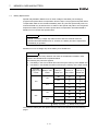
POINT
Make sure to back up each memory contents before storing the programmable
controller.
*
Refer to the following manuals for details of built-in RAM clear (PC memory all clear) memory
card format by peripheral devices.
GX Developer Operating Manual
A6GPP/A6PHP Operating Manual
SW IVD-GPPA Operating Manual
Refer to Section 4.6.3 for latch clear operation by RESET/L.CLR switch of the CPU module.
A - 15
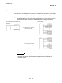
1.
OVERVIEW
1
OVERVIEW
This user's manual describes the performance, functions, and handling method of the
QCPU-A, as well as the specifications and handling of the memory card, power supply
module and the base module.
The programming modules and software packages have to be compatible with the
upgraded A2UCPU, A2UCPU-S1, A3UCPU, and A4UCPU (abbreviated as AnUCPU
hereafter).
When the conventional programming modules and software packages are used, the
usable range varies depending on the model of the CPU (programmable controller model
name). (Refer to Section Section 2.2.3.)
Related to each module used in the CPU modules, check "System equipment list" in
Section 2.3.
Refer to Section Section 2.2.1 for the special function modules which have limited usable
devices range.
(1)
Bundled parts
Product Name
Model
Quantity
Q02CPU-A
CPU module
Q02HCPU-A
1
Q06HCPU-A
Battery
Q6BAT
1-1
1
1.
OVERVIEW
1.1
Features
QCPU-A (A mode) has the following features compared with A2USHCPU-S1.
(1)
High-speed operation processing speed
QCPU-A offers significantly higher operation processing than that of A2USHCPU-S1.
Item
Operation processing
speed*1
*1
(2)
Q02HCPU-A,
Q02CPU-A
Q06HCPU-A
79ns
34ns
A2USHCPU-S1
90ns
I/O processing: At refresh or LD instruction
Greater program capacity
By using Q06HCPU-A, the program capacity can be expanded.
Moreover, Q06HCPU-A can create subprograms.
Item
Q06HCPU-A
A2USHCPU-S1
30k steps (Main program)
Program capacity
+
30k steps
30k steps (Subprogram)
(3)
Increased actual I/O points
QCPU-A offers 4096 actual I/O points, 4 times as increased as that of A2USHCPUS1.
Item
Q02CPU-A, Q02HCPU-A,
Q06HCPU-A
Actual I/O points
4096 points
A2USHCPU-S1
1024 points
(4)
Increased extension stages
Up to 7 stages of extension base module can be added.
(5)
Higher communication speed with peripheral devices
The communication speed with peripheral devices is considerably improved
compared with A2USHCPU-S1.
Item
Q02CPU-A, Q02HCPU-A,
Q06HCPU-A
Communication speed
115.2 *1
(kbps)
*1
Designate 9.6kbps when using GPP of SW3D5C-GPPW or earlier.
1-2
A2USHCPU-S1
9.6
2.
SYSTEM CONFIGURATION
2
SYSTEM CONFIGURATION
This chapter shows the system configuration of QCPU-A, the relevant precautions and
system equipment.
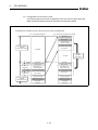
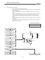
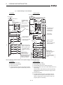
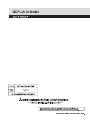
System Configuration
This section describes the configuration of the QCPU-A system, the configuration of
peripheral devices, and the overview of the system configuration.
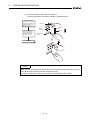
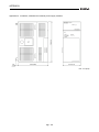
(1)
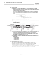
Configuration of the QCPU-A system
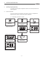
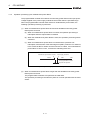
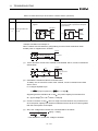
MITSUBISHI
LITHIUM BATTERY
MITSUBISHI
2.1
Memory card * 1
(Q2MEM-1MBS)
QCPU-A
(Q02CPU-A, Q02HCPU-A,
Q06HCPU-A)
Battery
(Q6BAT)
*1 The operation is not guaranteed
for the use of commercially
available memory cards.
Main base unit
(QA1S33B,QA1S35B,QA1S38B)
Expansion of AnS series modules
Extension base unit
(QA1S65B,QA1S68B)
Extension cable
(QC06B,QC12B,QC30B,
QC50B,QC100B)
AnS series power supply, I/O, or
special function modules
2-1
Q series power supply, I/O, or
intelligent function modules
2.
SYSTEM CONFIGURATION
2.2
Precautions When Configuring the System
The following shows the precautions when configuring the QCPU-A system:
2.2.1
Hardware
(1)
Up to 64 I/O modules or special function modules can be mounted to each of the
basic base unit or the expansion base unit.
(2)
Up to 7 extension base units can be connected in the system.
(Up to 8 modules including the main base unit.)
(3)
The total length of the extension cable should be 13.2m (43.31ft.) or less.
(4)
The following shows the modules that have some limitations for the number of
modules to be mounted.
Module
No. of Mountable Modules
MELSECNET/10 network module
A1SJ71LP21(GE), A1SJ71LR21,
Up to 4 modules
A1SJ71BR11
Up to 4 modules in
MELSECNET(II)/B data link module
total
A1SJ71AP21, A1SJ71AR21,
Up to 2 modules
A1SJ71AT21B
Interruption module: A1SI61
1 module
AnS series special function module*1
Up to 6 modules in total
GOT-A900 Series (Only when the bus
connection is used.)*2
GOT1000 Series (Only when the bus
Connection disable
connection is used.)*2
*1
*2
Applies to the following modules. Any modules but the following modules do not have the
number of limitations to be mounted.
Ethernet interface module: A1SJ71E71N-B2 (-B5/-T)
Calculating machine link module: A1SJ71UC24-R2 (-R4/-PRF)
CC-Link module (in intelligent mode): A1SJ61BT11
Intelligent communication module: A1SD35ID1(2)
ID interface module: A1SD35ID1(2)
Refer to the following manual for the GOT models.
• GOT-A900 Series User's Manual (GT Works Versions2/GT Designer2 Version2 Compatible
Connection System Manual)
• GOT1000 Series Connection Manual (Mitsubishi Products)
2-2
2.
SYSTEM CONFIGURATION
(5)
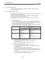
The accessible device ranges have limit when the following modules are used:
Accessible Device Range in CPU
Applicable Module
Device
MELSECNET(II) data link module:
A1SJ71AP21, A1SJ71AR21
MELSECNET/B data link module:
A1SJ71AT21B
(6)
Accessible Range
Input (X), output (Y)
X/Y0 to X/Y7FF
Internal relay (M)
M0 to M8191
latch relay (L)
L0 to L8191
Link relay (B)
B0 to BFFF
Timer (T)
T0 to T2047
Counter (C)
C0 to C1023
Data register (D)
D0 to D6143
Link register (W)
W0 to WFFF
Annunciator (F)
F0 to F2047
It is recommended that the network and data link modules are mounted to the basic
base unit.
When these modules are mounted to the extension base unit, the link refresh time
becomes longer than the case where they are mounted to the basic base unit.
2-3
2.
2.2.2
SYSTEM CONFIGURATION
Software package
(1)
GPP function software packages and model name setting at the start-up
The following table shows the GPP function software package that can be used to
create the QCPU-A program, and the programmable controller type setting at startup.
When using SW4D5C-GPPW or later, select the programmable controller type from
Q02(H)-A or Q06H-A according to the CPU to be used.
When using the peripheral devices and GPP function software package of SW3D5CGPPW or earlier, specify the programmable controller type name as "A4U". If "A4U"
is not found in PLC type names, specify "A3A." If both "A4U" and "A3A" are not
found, specify "A3H."
Note that when "A4U" is specified, the available device range is limited.
Programmable controller CPU
Peripheral
device
PC/AT
personal
computer
Software package for system start-up
Q02(H)-A
Q06H-A
Q02(H)-A
Q06H-A
A4U
A4U
SW3GP-GPPA
A3H
A3H
SW4GP-GPPA
A3A
A3A
SW1GP-GPPAU
A4U
A4U
A3H
A3H
SW4GP-GPPA
A3A
A3A
SW1GP-GPPAU
A4U
A4U
SW4D5C-GPPW or later
SW3D5
SW
A6PHP
A6GPP
model setting
-GPPW or earlier
IVD-GPPA
SW3-GPPA
SW3GP-GPPA
2-4
2.
SYSTEM CONFIGURATION
POINT
(1) Old software packages other than listed above cannot be used.
(2) To construct MELSECNET/10 network system with QCPU-A, use the AnUcompatible GPP function software package (which includes "A4U" in its
programmable controller type name).
A network cannot be constructed with the GPP function software package
which is not compatible with AnU (which does not include "A4U" in its
programmable controller type name).
(3) Communication with GX Developer at 115.2kbps may not be available
depending on the peripheral devices. In such a case, select the lower
communication speed.
(4) When using Q02(H)CPU-A and conventional peripheral devices and setting
the programmable controller type as "A4U," designate the main program
setting to 28k steps or less with parameters. When "Main + parameter" is
written with the programmable controller with the setting of 29k steps or more,
"Cannot communicate with PC" is displayed, and writing to the CPU module is
disabled.
(5) Subprograms cannot be used with Q02(H)CPU-A. When using conventional
peripheral devices and setting the programmable controller type as "A4U," do
not specify any subprograms. If any subprograms are specified, "Cannot
communicate with PC" is displayed.
With Q06HCPU, subprogram 1 can be used, but subprograms 2 and 3
cannot.
When subprogram 2 or 3 is specified, the same message above is displayed.
2-5
2.
SYSTEM CONFIGURATION
(2)
Utility package
(a) None of the following utility packages for A6GPP/A6PHP can be used:
• SW
-AD57P
• SW
-UTLP-FN0
* The packages marked with * can
execute the same functions using the
*
dedicated instructions.
• SW
-UTLP-FN1
• SW
-UTLP-PID
For details, refer to type AnSHCPU/
• SW
-SIMA
AnACPU/AnUCPU/QCPU-A (A Mode)
• SW
-UTLP-FD1
Programming Manual (Dedicated
• SW
-SAPA
Instructions).
POINT
(1) The utility package, which specifies the device and accesses the QCPU-A,
can be used only in the device range for the A3ACPU, A3HCPU equivalent.
(Refer to Section 2.2.3.)
(2) Use an AnU-compatible utility package to use the device range for the
QCPU-A.
(Example: SW1IVD-SAP2, etc.)
2-6
2.
SYSTEM CONFIGURATION
2.2.3
Precautions when using GPP function software packages and A8PUE peripheral devices which are
not compatible with AnU
When starting with GPP function software packages not compatible with the AnU, QCPUA (starting with the programmable controller model name "A3A" or "A3H") or a A8PUE
peripheral device (including A7PUS), the usable device ranges are limited as follows.
(1)
List of usable device range
AnACPU-compatible Module
A3HCPU-compatible Module
Programmable controller Model
Item
Programmable controller Model
"A3A"
A8PUE
at System FD Start-up
Instruction (sequence/basic/
"A3H"
A7PUS
at System FD Start-up
All instructions can be used.
application/dedicated)
Program capacity
Max. 14k steps can be used for the main program.
I/O device points (X/Y)
M, L, S relay
X/Y0 to X/Y7FF can be used.
X/Y0 to X/Y7FF can be used.
(X/Y800 to X/Y1FFF cannot be used.)
(X/Y800 to X/Y1FFF cannot be used.)
M/L/S0 to M/L/S2047 can be used.
M/L/S0 to M/L/S8191 can be used.
Link relay (B)
B0 to BFFF can be used.
B0 to B3FF can be used.
(B1000 to B1FFF cannot be used.)
(B400 to B1FFF cannot be used.)
Timer (T)
T0 to T2047 can be used.
Counter (C)
C0 to C1023 can be used.
Data register (D)
Link register (W)
Annunciator (F)
(M/L/S2048 to M/L/S8191 cannot be used.)
T0 to T255 can be used.
(T256 to T2047 cannot be used.)
C0 to C255 can be used.
(C256 to C1023 cannot be used.)
D0 to D6143 can be used.
D0 to D1023 can be used.
(D6144 to D8191 cannot be used.)
(D1024 to D8191 cannot be used.)
W0 to WFFF can be used.
W0 to W3FF can be used.
(W1000 to W1FFF cannot be used.)
(W400 to W1FFF cannot be used.)
F0 to F255 can be used.
F0 to F2047 can be used.
Index register (V, Z)
(F256 to F2047 cannot be used.)
V, V1 to V6, Z, Z1 to Z6can be used.
Expanded comment
Max. 3968 points
Latch (power failure compensation)
range
–
Unusable
–
The device range shown above can be latched. The device range shown above can be latched.
Possible to register occupied I/O
I/O assignment
V and Z can be used.
(V1 to V6, Z1 to Z6 cannot be used.)
points and module model names.
–
Number of I/O occupied points can
be registered.
–
(1)
The device range other than listed above is the same as that of QCPU-A.
(2)
Refer to Operating Manual for peripheral devices to be used for available functions.
2-7
2.
SYSTEM CONFIGURATION
2.3
System Equipment
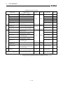
The following shows various components of each module and peripheral device which can
be used by the QCPU-A.
(1)
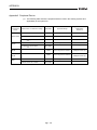
Product Name
Modules dedicated to AnS
Model Name
Number of Occupied
Points (points)
[I/O Assignment
Module Type]
Description
Current Consumption
Remark
5VDC(A) 24VDC(A)
Q02CPU-A
Program capacity: 28k steps, I/O points: 4096,
Processing speed for basic instruction: 79ns
–
0.60
–
Q02HCPU-A
Program capacity: 28k steps, I/O points: 4096,
Processing speed for basic instruction: 34ns
–
0.64
–
Q06HCPU-A
Program capacity: 30k steps 2 (Main/sub),
I/O points: 4096, Processing speed for basic
instruction: 34ns
–
0.64
–
Q2MEM-1MBS
SRAM type: 1MB
–
–
–
QA1S33B
AnS series module mounting base (power
supply module + CPU module + 3 slots for other
module)
–
0.107
–
QA1S35B
AnS series module mounting base (power
supply module + CPU module + 5 slots for other
module)
–
0.117
(0.086)*
–
QA1S38B
AnS series module mounting base (power
supply module + CPU module + 8 slots for other
module)
–
0.118
(0.086)*
–
QA1S65B
AnS series module mounting base (power
supply module + CPU module + 5 slots for other
module)
–
0.117
(0.088)*
–
QA1S68B
AnS series module mounting base (power
supply module + CPU module + 8 slots for other
module)
–
0.118
(0.090)*
–
QC06B
0.6m (1.97ft.) extension base cable
–
–
–
QC12B
1.2m (3.94ft.) extension base cable
–
–
–
Extension cable QC30B
3.0m (9.84ft.) extension base cable
–
–
–
QC50B
5.0m (16.40ft.) extension base cable
–
–
–
QC100B
10.0m (32.81ft.) extension base cable
–
–
–
Battery
Q6BAT
Battery for retaining the contents of built-in RAM
and devices in case of power failure
–
–
–
Cable
QC30R2
Communication cable for peripheral devices
–
–
–
CPU module
Memory card
Main base unit
Extension base
unit
2-8
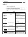
2.
SYSTEM CONFIGURATION
Product Name
Power supply
module
Model Name
Number of Occupied
Points (points)
[I/O Assignment
Module Type]
Description
A1S61PN
5VDC, 5A
A1S62PN
5VDC, A/24VDC, 0.6A
A1S63P
5VDC, 5A
*
100/200VAC
input
–
Current Consumption
Remark
5VDC(A) 24VDC(A)
–
–
24VDC input
Installed in the
power supply
slot of the main
base and
extension base.
The parenthesized values are for those which is not compliant with CE.
POINT
(1) A USB port cannot be used with QCPU-A.
(2) A RS232/422 conversion cable is required to use the conventional peripheral
devices (A6GPP, A8PUE, etc.).
Recommended cable: FA-CNV2402CBL (2m (6.56ft.)), FA-CNV2405CBL (5m
(16.40ft.))
Contact: Mitsubishi Electric Engineering Corp.
2-9
2.
SYSTEM CONFIGURATION
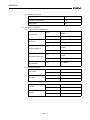
Product Name
Input module
Model Name
Number of Occupied
Points (points)
[I/O Assignment
Module Type]
Description
Current Consumption
Remark
5VDC(A) 24VDC(A)
A1SX10
16-point 100 to 120 VAC input module
16
[16 input points]
0.05
–
A1SX10EU
16-point 100 to 120 VAC input module
16
[16 input points]
0.05
–
A1SX20
16-point 200 to 240 VAC input module
16
[16 input points]
0.05
–
A1SX20EU
16-point 200 to 240 VAC input module
16
[16 input points]
0.05
–
A1SX30
16-point 12/24VDC, 12/24VAC input module
16
[16 input points]
0.05
–
A1SX40
16-point 12/24VDC input module
16
[16 input points]
0.05
–
A1SX40-S1
16-point 24VDC input module
16
[16 input points]
0.05
–
A1SX40-S2
16-point 24VDC input module
16
[16 input points]
0.05
–
A1SX41
32-point 12/24VDC input module
32
[32 input points]
0.08
–
A1SX41-S1
32-point 24VDC input module
32
[32 input points]
0.12
–
A1SX41-S2
32-point 24VDC input module
32
[32 input points]
0.08
–
A1SX42
64-point 12/24VDC input module
64
[64 input points]
0.09
–
A1SX42-S1
64-point 24VDC input module
64
[64 input points]
0.16
–
A1SX42-S2
64-point 24VDC input module
64
[64 input points]
0.09
–
A1SX71
32-point 5/12/24VDC input module
32
[32 input points]
0.075
–
A1SX80
16-point 12/24VDC sink/source input module
16
[16 input points]
0.05
–
A1SX80-S1
16-point 24VDC sink/source input module
16
[16 input points]
0.05
–
A1SX80-S2
16-point 24VDC sink/source input module
16
[16 input points]
0.05
–
A1SX81
32-point 12/24VDC sink/source input module
16
[16 input points]
0.08
–
A1SX81-S2
32-point 24VDC sink/source input module
32
[32 input points]
0.08
–
A1SX82-S1
64-point 24VDC sink/source input module
32
[32 input points]
0.16
–
2 - 10
2.
SYSTEM CONFIGURATION
Product Name
Model Name
Number of Occupied
Points (points)
[I/O Assignment
Module Type]
Description
Current Consumption
Remark
5VDC(A) 24VDC(A)
A1SX10
16-point relay contact output module (2A)
16
[16 output
points]
0.12
0.09
A1SY10EU
16-point relay contact output module (2A)
16
[16 output
points]
0.12
0.10
A1SY14EU
12-point relay contact output module (2A)
16
[16 output
points]
0.12
0.10
A1SY18A
8-point relay contact output module (2A) for
independent contacts
16
[16 output
points]
0.24
0.075
A1SY18AEU
8-point relay contact output module (2A) for
independent contacts
16
[16 output
points]
0.24
0.075
A1SY22
16-point triac output module (0.6A)
16
[16 output
points]
0.27
(200VAC)
0.002
A1SY28A
8-point triac output module (1A)
All points independent
16
[16 output
points]
0.13
–
A1SY40
16-point 12/24VDC transistor output module
(0.1A) sink type
16
[16 output
points]
0.27
0.008
A1SY40P
16-point 12/24VDC transistor output module
(0.1A) sink type
16
[16 output
points]
0.08
0.011
A1SY41
32-point 12/24VDC transistor output module
(0.1A) sink type
32
[32 output
points]
0.50
0.008
A1SY41P
32-point 12/24VDC transistor output module
(0.1A) sink type
32
[32 output
points]
0.14
0.012
A1SY42
64-point 12/24VDC transistor output module
(0.1A) sink type
64
[64 output
points]
0.93
0.008
A1SY50
16-point 12/24VDC transistor output module
(0.5A) sink type
16
[16 output
points]
0.12
0.06
A1SY60
16-point 24VDC transistor output module
(2A) sink type
16
[16 output
points]
0.12
0.015
A1SY60E
16-point 12/24VDC transistor output module
(2A) source type
16
[16 output
points]
0.20
0.01
A1SY68A
8-point 5/12/24/48VDC
transistor output module (2A) sink/source type
All points independent
16
[16 output
points]
0.11
–
A1SY71
32-point 5/12VDC transistor output module
(0.016A) sink type
32
[32 output
points]
0.40
0.15
A1SY80
16-point 12/24VDC transistor output module
(0.8A) source type
16
[16 output
points]
0.12
0.02
A1SY81
32-point 12/24VDC transistor output module
(0.1A) source type
32
[32 output
points]
0.50
0.008
A1SY82
64-point 12/24VDC transistor output module
(0.1A) source type
64
[64 output
points]
0.93
0.008
Output module
2 - 11
2.
SYSTEM CONFIGURATION
Product Name
Model Name
Current Consumption
Remark
5VDC(A) 24VDC(A)
A1SH42
32-point 12/24VDC input module
32-point 12/24VDC transistor output module
(0.1A) sink type
32
[32 output
points]
0.50
0.008
A1SH42-S1
32-point 24VDC input module
32-point 12/24VDC transistor output module
(0.1A) sink type
32
[32 output
points]
0.50
0.008
A1SX48Y18
8-point 24VDC input module
8-point relay contact output module (2A)
16
[16 output
points]
0.085
0.045
A1SX48Y58
8-point 24VDC input module
8-point 12/24VDC transistor output module
(0.5A)
16
[16 output
points]
0.06
0.06
A1S42X
16/32/48/64 points
12/24VDC dynamic input module
0.08
–
0.18
0.055
–
–
–
–
I/O combined
module
Dynamic input
module
Number of Occupied
Points (points)
[I/O Assignment
Module Type]
Description
Dynamic output
A1S42Y
module
16/32/48/64 points
12/24VDC dynamic output module
Blank cover
Dust-proof cover for unused slot
A1SG60
Specified number of points
[Input
Specified number of points ]
Specified number of points
[Output
Specified number of points ]
16
[Empty]
Dummy module A1SG62
Specified number of points
16-point, 32-point, 48-point, 64-point selectable [Input
module
Specified number of points ]
Pulse catch
module
A1SP60
Short ON-time pulse input module
16
(pulse with a minimum of 0.5ms) 16 input points
[16 output
points]
0.055
–
Analog timer
module
A1ST60
A module whose timer setting value can be
changed for different volumes (0.1 to 1.0s, 1 to
10s, 10 to 60s, 60 to 600s)
Analog timer 8 points
16
[16 output
points]
0.055
–
Interrupt
module
A1SI61
Interrupt module for specifying the interrupt
program
(16-point interrupt input)
32
[32 special
points]
0.057
–
A1SD61
32-bit signed binary
50kBPS, 1 channel
32
[32 special
points]
0.35
–
A1SD62
24-bit signed binary, 2 channel
100kPPS, DC input
transistor output (sink type)
32
[32 special
points]
0.1
–
24-bit signed binary, 2 channel
200kPPS, difference input
transistor output (sink type)
32
[32 special
points]
0.25
–
A1SD62D-S1
24-bit signed binary, 2 channel
200kPPS, difference input
transistor output (sink type)
32
[32 special
points]
0.27
–
A1SD62E
24-bit signed binary, 2 channel
100kPPS, DC input
transistor output (source type)
32
[32 special
points]
0.1
–
High-speed
A1SD62D
counter module
2 - 12
2.
SYSTEM CONFIGURATION
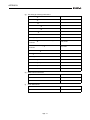
Product Name
Model Name
Remark
5VDC(A) 24VDC(A)
4 to 20mA/0 to 10V
4 analog channels
32
[32 special
points]
0.4
–
A1S68AD
4 to 20mA/0 to 10V
8 analog channels
32
[32 special
points]
0.4
–
A1S62DA
4 to 20mA/0 to 10V
2 analog output channels
32
[32 special
points]
0.8
–
A1S68DAV
-10 to 10V input
8 analog output channels
32
[32 special
points]
0.65
–
A1S68DAI
4 to 20mA input
8 analog output channels
32
[32 special
points]
0.85
–
A1S63ADA
Analog input, 2 channels, simple loop control is
allowed
32
1 analog output channels
[32 special
points]
0.8
–
A1S66ADA
Analog input, 4 channels, simple loop control is
allowed
32
2 analog output channels
[32 special
points]
0.21
0.16
A1S62RD3
For connecting to Pt100 (3-wire)
Temperature input, 2 channels
32
[32 special
points]
0.49
–
A1S62RD4
For connecting to Pt100 (4-wire)
Temperature input, 2 channels
32
[32 special
points]
0.39
–
A1S68TD
Thermocouple input, 8 channels
32
[32 special
points]
0.32
–
A1S62TCTT-S2
Transistor output, thermocouple input
2 channels/module
PID control: ON/OFF pulse
32
[32 special
points]
0.19
–
32
[32 special
points]
0.28
–
32
[32 special
points]
0.19
–
Transistor output, platinum RTD input
A1S62TCRTBW- 2 channels/module
S2
PID control: ON/OFF pulse, wire breakage
detection function
32
[32 special
points]
0.28
–
Transistor output, thermocouple input
4 channels/module
PID control: ON/OFF pulse or 2 positioning
control
32
[32 special
points]
0.33
–
Transistor output, thermocouple input
4 channels/module
A1S64TCTTBWPID control: ON/OFF pulse or 2 positioning
S1
control
Heater wire breakage detection function
32
[32 special
points]
0.42
–
Analog I/O
module
Transistor output, thermocouple input
A1S62TCTTBW- 2 channels/module
PID control: ON/OFF pulse, wire breakage
S2
detection function
Temperature
control module
Current Consumption
A1S64AD
A/D converter
module
D/A converter
module
Number of Occupied
Points (points)
[I/O Assignment
Module Type]
Description
A1S62TCRT-S2
A1S64TCTT-S1
Transistor output, platinum RTD (Resistance
Temperature Detector) input
2 channels/module
PID control: ON/OFF pulse
2 - 13
2.
SYSTEM CONFIGURATION
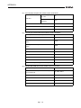
Product Name
Model Name
Ethernet
interface
module
Intelligent
communication
module
Remark
5VDC(A) 24VDC(A)
32
[32 special
points]
0.33
–
Transistor output, thermocouple input
4 channels/module
A1S64TCRTBWPID control: ON/OFF pulse or 2 positioning
S1
control
Heater wire breakage detection function
32
[32 special
points]
0.42
–
Transistor output,
thermocouple input, or platinum RTD input
[For standard control]
4 channels/module
PID control: ON/OFF pulse or 2 positioning
control
[For heating-cooling control]
2 channels/module
PID control: ON/OFF pulse
32
[32 special
points]
0.33
(0.19)*
–
Transistor output,
thermocouple input, or platinum RTD input
[For standard control]
4channels/module
PID control: ON/OFF pulse or 2 positioning
control
[For heating-cooling control]
2 channels/module
PID control: ON/OFF pulse, wire breakage
detection function
32
[32 special
points]
0.39
(0.25)*
–
A1SJ71UC24-R2 Computer link function RS-232C, 1 channel
32
[32 special
points]
0.1
–
A1SJ71UC24PRF
Computer link function, printer function
RS-232C, 1 channel
32
[32 special
points]
0.1
–
A1SJ71UC24-R4
Computer link function, multidrop link function
RS-422/RS-485, 1 channel
32
[32 special
points]
0.1
–
A1SJ71E71N3-T 10 Base-T
32
[32 special
points]
0.69
–
A1SJ71E71N-T
32
[32 special
points]
0.56
–
A1SJ71E71N-B2 10 Base 2 (for Cheapernet)
32
[32 special
points]
0.66
–
A1SJ71E71N-B5 10 Base 5 (for Ethernet)
32
[32 special
points]
0.57
–
32
[32 special
points]
0.4
–
A1S64TCTRT
A1S64TCTRTB
W
Computer link
module
Current Consumption
Transistor output, thermocouple input
4 channels/module
PID control: ON/OFF pulse or 2 positioning
control
A1S64TCRT-S1
Temperature
control module
Number of Occupied
Points (points)
[I/O Assignment
Module Type]
Description
A1SD51S
10 Base-T
BASIC (interpreter/compiler)
RS-232C, 2 channel
RS-422/RS485, 1 channel
2 - 14
*:When the
temperature
conversion
function of
unused channels
are not used in
the heatingcoolA1S64TCTR
TBWing control
Accessible
within the
AnACPU device
range
2.
SYSTEM CONFIGURATION
Product Name
Model Name
A1SD70
1 axis positioning control, speed control and
speed-positioning control,
analog voltage output for speed-positioning
control (0 to
Positioning
module
Number of Occupied
Points (points)
[I/O Assignment
Module Type]
Description
10V)
Remark
5VDC(A) 24VDC(A)
0.3
–
A1SD75P1-S3
For positioning control, pulse output, 1-axis
32
[32 special
points]
0.7
–
A1SD75P2-S3
For positioning control, pulse output, 2-axes
(independent, 2-axis simultaneous, linear
interpolation, circular interpolation)
32
[32 special
points]
0.7
–
A1SD75P3-S3
For positioning control, pulse output, 3-axis
(independent, 3-axis simultaneous, 2-axis linear 32
interpolation, 2-axis circular interpolation)
[32 special
points]
0.7
A1SD75M1
For positioning control, digital output for MR-H32
B/MR-J-B/MR-J2-B, 1-axis SSCNET
[32 special
points]
0.7
–
A1SD75M2
For positioning control, digital output, for MR-HB/MR-J-B/MR-J2-B, 2-axis SSCNET
32
(Independent, 2-axis simultaneous, linear
interpolation, circular interpolation)
[32 special
points]
0.7
–
A1SD75M3
For positioning control, digital output, for MR-HB/MR-J-B/MR-J2-B, 3-axis SSCNET
32
(independent, 3-axis simultaneous, 2-axis linear
interpolation, 2-axis circular interpolation)
[32 special
points]
0.7
–
A1SD35ID1
ID interface module
One reader/writer modules can be connected.
32
[32 special
points]
0.25
0.17
A1SD35ID2
ID interface module
Two reader/writer modules can be connected.
32
[32 special
points]
0.25
0.33
A1SJ71AP21
For the master and local stations of
MELSECNET(II) data link system (for the
optical fiber cable)
32
[32 special
points]
0.33
–
32
[32 special
points]
0.33
–
ID interface
module
For the master and local stations of
MELSECNET(II)
A1SJ71AP21-S3 MELSECNET(II) data link
data link
(for the GI-type optical fiber cable)
module
MELSECNET/B
data link
module
48
First half
16 empty points
Second half
32 special points
Current Consumption
*
–
A1SJ71AR21
For the master and local stations of
MELSECNET(II) data link system (for the
coaxial cable)
32
[32 special
points]
0.8
–
A1SJ71AT21B
For the master and local stations of
MELSECNET/B data link system
32
[32 special
points]
0.66
–
A1SJ72T25B
For the remote I/O station of
MELSECNET/B data link system
0.3
–
0.08
–
B/NET data link
A1SJ71B62-S3
module
–
Master module for B/NET
32
2 - 15
[32 special
points]
* When different
driver is
connected:
0.78A
Access is
allowed within
the device range
of the AnACPU.
2.
SYSTEM CONFIGURATION
Product Name
Model Name
Number of Occupied
Points (points)
[I/O Assignment
Module Type]
Description
Current Consumption
Remark
5VDC(A) 24VDC(A)
A1SJ71LP21
For the control, master, and normal stations of
the MELSECNET/10 data link module system
(For the dual loop SI-type optical fiber cable)
32
[32 special
points]
0.65
–
A1SJ71LP21GE
For the control, master, and normal stations of
the MELSECNET/10 data link module system
(For the dual loop GI-type optical fiber cable)
32
[32 special
points]
0.65
–
A1SJ71BR11
For the control, master, and normal stations of
the MELSECNET/10 data link module system
(For the single bus coaxial cable)
32
[32 special
points]
0.80
–
A1SJ71LR21
For the control, master, and normal stations of
the MELSECNET/10 data link module system
(For the coaxial cable dual loop)
32
[32 special
points]
1.14
–
For the master and local stations of the CC-Link
data link system
32
(For the twisted pair shield cable only)
[32 special
points]
0.40
–
0.35
–
MELSECNET/10
data link
module
CC-Link system
A1SJ61BT11
master module
For MELSECNET/MINI-S3 master stations
MELSECNET/
(max. 64 stations). Performs remote I/O and
MINI-S3 master A1SJ71PT32-S3
remote terminal control of a total of 512 I/O
module
points.
I/O mode
32 [32 special points]
Expanded mode
48 [48 special points]
MELSECNET-I/
O LINK master A1SJ51T64
module
MELSECNET-I/O LINK master station. Controls
I/O LINK remote I/O module of a maximum of
64 stations and a total of 128 I/O points.
If only a few remote I/O units are used, perform 64
I/O assignment with a peripheral device to
decrease the number of occupied I/O points to
16, 32, or 48.
[64 output
points]
0.115
0.09
S-LINK
interface
module
A1SJ71SL92N
Master module for S-LINK
I/O total 128 points
32
[32 special
points]
0.20
–
AS-I interface
module
A1SJ71AS92
Master module for AS-I
I/O total 496 points
32
[32 special
points]
0.15
–
Positioning
detection
module
A1S62LS
Absolute positioning detection module
32
[32 special
points]
0.55
–
Programmable controller easier monitoring
module
16
[16 output
points]
0.08
–
Programmable
controller easier
A1SS91
monitoring
module
Memory card
interface
module
Simulation
module
A1SD59J-S2
Memory card interface module
32
A6SIM-X64Y64
An I/O simulation unit used connected to the
base module Debugging can be executed
64
without connecting the I/O module to the base
64
module. Use an extension cable of the AnS
series between the main base of the AnS series
and the A6SIM-X64Y64.
2 - 16
[32 special
points]
[64 input points]
[64 output
points]
0.05
–
TYP. 0.3
(When all
points
"ON")
–
The current
consumption
describes in
connecting
A1SD59J-MIF.
2.
SYSTEM CONFIGURATION
Product Name
PROFIBUS
interface
module
Device net
interface
module
MODBUS
interface
module
Graphic
operation
terminal
Model Name
Number of Occupied
Points (points)
[I/O Assignment
Module Type]
Description
Current Consumption
Remark
5VDC(A) 24VDC(A)
A1SJ71PB92D
PROFIBUS-DP master module
32
[32 special
points]
0.56
–
A1SJ71PB96F
PROFIBUS-FMS interface module
32
[32 special
points]
0.56
–
A1SJ71DN91
Device net master module
32
[32 special
points]
0.24
–
A1SJ71UC24R2-S2
RS-232Ctype MODBUS interface module
32
[32 special
points]
0.1
–
A1SJ71UC24R4-S2
RS-422/485type MODBUS interface module
32
[32 special
points]
0.1
–
–
–
–
–
–
–
–
–
For the applicable GOT models, refer to
GOT1000 Series GOT1000 Series Connection Manual
(Mitsubishi Products).
GOT-A900
Series
For the applicable GOT models, refer to
GOT-A900 Series User's Manual.
(GT Work2 Version2/GT Designer2 Version2
Compatible Connection System Manual)
2 - 17
2.
SYSTEM CONFIGURATION
Product Name
Model Name
A6TBXY36
Connector/terminal
block converter unit
Cable for
connector/terminal
block converter unit
Relay terminal unit
Cable for
connecting the
relay terminal unit
Terminal block
cover for the A1S I/
O module and the
special module
Description
Applicable Model
For the sink-type input module and sink-type output
module. (standard type)
A1SX41(S1/S2), A1SX42(S1/S2), A1SY41, A1SY41P,
A1SY42, A1SY82, A1SH42(S1)
A6TBXY54
For the sink-type input module and sink-type output
module. (2-wire type)
A6TBX70
For the sink-type input module (3-wire type)
A1SX41(S1/S2), A1SX42(S1/S2), A1SH42(S1)
A6TBX36-E
For the source-type input module (standard type)
A1SX71, A1SX82-S1, A1SX81(S2)
A6TBY36-E
For the source-type output module (standard type)
A1SY81, A1SY82
A6TBX54-E
For the source-type input module (2-wire type)
A1SX71, A1SX82-S1, A1SX81(S2)
A6TBY54-E
For the source-type output module (2-wire type)
A1SY81, A1SY82
A6TBX70-E
For the source-type input module (3-wire type)
A1SX71, A1SX82-S1, A1SX81(S2)
AC05TB
0.5m (1.64ft.) for the sink module
AC10TB
1m (3.28ft.) for the sink module
AC20TB
2m (6.56ft.) for the sink module
AC30TB
3m (9.84ft.) for the sink module
AC50TB
5m (16.40ft.) for the sink module
AC80TB
8m (26.24ft.) for the sink module
AC100TB
10m (32.81ft.) for the sink module
AC05TB-E
0.5m (1.64ft.) for the source module
AC10TB-E
1m (3.28ft.) for the source module
AC20TB-E
2m (6.56ft.) for the source module
AC30TB-E
3m (9.84ft.) for the source module
AC50TB-E
5m (16.40ft.) for the source module
A6TE2-16SRN
For the sink-type output module
AC06TE
0.6m (1.97ft.) long
AC10TE
1m (3.28ft.) long
AC30TE
3m (9.84ft.) long
AC50TE
5m (16.40ft.) long
AC100TE
10m (32.81ft.) long
A1STEC-S
Slim-type terminal block cover for the A1S I/O
module and the special module (terminal block
connector type).
A6TBXY36
A6TBXY54
A6TBX70
A6TBX36-E
A6TBY36-E
A6TBX54-E
A6TBY54-E
A6TBX70-E
A1SY41, A1SY41P, A1SY42, A1SH42(S1)
A6TE2-16SRN
2 - 18
All terminal block connector type modules
2.
SYSTEM CONFIGURATION
Product Name
IDC terminal block
adapter
Terminal block
adapter
Model Name
Description
Applicable Model
A1S-TA32
IDC terminal block adapter for 32 points 0.5mm2
(AWG20)
A1S-TA32-3
IDC terminal block adapter for 32 points 0.3mm2
(AWG22)
A1S-TA32-7
IDC terminal block adapter for 32 points 0.75mm2
(AWG18)
A1S-TB32
For 32 points, conversion into Europe type terminal
block
A6C0N1
Soldering-type, straight out
A6C0N2
Crimp type, straight out
A6C0N3
Insulation-displacement type, flat cable
A6CON4
Soldering-type, straight/diagonal out
A6C0N1E
Soldering-type, straight out
A6C0N2E
Crimp type, straight out
A6C0N3E
Insulation-displacement type, flat cable
40-pin connector
3-pin D-sub
connector
A1SX41(S1/S2), A1SX71, A1SY41, A1SY41P, A1SY71
A1SX41(S1/S2), A1SX71, A1SY41, A1SY41P, A1SY71
Sink type (40p FCN)
Source type (37p D-sub)
REMARK
Toa Electric Industrial CO., LTD. provides I/O cables with connectors, which can
connect to 40-pin connector (A1SX41, A1SX42, A1SY41, A1SY41P, A1SY42,
A1SY42P, etc.) or 37-pin D-sub connector (A1SX81, A1SY81) of I/O modules.
Contact:
TOA ELECTRIC INDUSTRIAL CO., LTD.
2 - 19
2.
SYSTEM CONFIGURATION
(2)
Peripheral device
Product Name
Model Name
Remark
A6PHP-SET
•
•
•
•
•
A6PHP main unit
SWGP-GPPA...............
SWGP-GPPK...............
SW0-GPPU..................
AC30R4........................
GPP function start-up floppy disk for the A series
GPP function start-up floppy disk for the K series
User floppy disk (2DD)
3m (9.84ft.)-long RS-422 cable
Intelligent GPP
A6GPP-SET
•
•
•
•
•
A6GPP main unit
SWGP-GPPA...............
SWGP-GPPK...............
SW0-GPPU..................
AC30R4........................
GPP function start-up floppy disk for the A series
GPP function start-up floppy disk for the K series
User floppy disk (2DD)
3m (9.84ft.)-long RS-422 cable
Composite video cable
AC10MD
• Connection cable for the monitor display of the A6GPP screen: 1m (3.28 ft.)long
Plasma hand-held
graphic programmer
AC30R4
3m (9.84ft.) long
AC300R4
30m (98.43ft.) long
User floppy disk
SW0S-USER
2HD-type
Floppy disk for storing user programs
(3.5-inch, pre-formatted)
Cleaning floppy disk
SW0-FDC
For A6GPP/A6PHP
Floppy disk for cleaning the floppy disk drive
RS-422 cable
Optional keyboard for
A6PHP
A6KB-SET-H
Connection cable for between the CPU main module and
A6GPP/A6PHP
• A6KB keyboard
• AC03R4H...................
• A6KB-C.......................
Optional keyboard for
A6GPP
A6KB-SET
• A6KB keyboard
• AC03R4L....................
• A6KB-C.......................
2 - 20
0.3m (0.98 ft.)-long connection cable between A6KB
and A6PHP
Key sheet for the GPP mode of A6KB
0.3m (0.98 ft.)-long connection cable between A6KB
and A6GPP
Key sheet for the GPP mode of A6KB
2.
SYSTEM CONFIGURATION
Product Name
Model Name
Remark
Printer
K6PR-K
A7NPR-S1
RS232C cable
AC30R2
Connection cable for between A6GPP/A6PHP and printer (K6PR-K, A7NPR-S1,
and a general-purpose printer with RS-232C interface)
3m (9.84ft.) long
Printer paper
K6PR-Y
K7PR-Y
Printer paper for K6PR(S1) and K6PR-K. 9-inch paper 2000 sheets per unit.
Printer paper for A7PR and A7NPR 11-inch paper Unit: 2000 sheets
Inked ribbon for
K6PR(K)
K6PR-R
Replacement inked ribbon for K6PR-K.
A7PUS
Read/write of the program is performed by connecting to the CPU main module
with a RS-422 cable (AC30R4-PUS). (5VDC 0.4A)
A8PUE
Read/write of the program is performed by connecting to the CPU main module or
a RS-422 cable (AC30R4-PUS, AC20R4-A8PU). (5VDC 0.4A)
AC30R4-PUS
Connection cable for between the CPU main module and A7PUS, A8PUE.
3m (9.84ft.) long
AC20R4-A8PU
Connection cable for between the CPU main module and A8PUE.
2m (6.56ft.) long
• For printing out program circuit diagrams and various lists
Programming module
RS-422 cable
Data access module
A6DU-B
• Used for monitoring the devices of the CPU module, changing the setting values/
current values, and displaying the operation status. (5VDC 0.23A)
• Connect to the CPU module with an AC30R4-PUS cable.
Modem interface
module
A6TEL
• An interface module which connects the CPU module and the modem. Using a
telephone line, the communication is performed between a remote peripheral
device and the CPU module. (5VDC 0.2A)
• Connect to the CPU module with an AC30R4-PUS cable.
RS-422 cable
AC30R4
AC300R4
Connection cable for between the CPU main module and A6WU 3m/30m (9.84 ft./
98.43 ft.) long.
AC03WU
Connection cable for between the A6PHP main unit and A6WU 0.3m (0.98ft.) long
2 - 21
2.
SYSTEM CONFIGURATION
2.4
System Configuration Overview
There are four system configuration types as follows:
(1)
Stand-alone system
.............. A system with a main base module only, or with a main
base system and an extension base module connected
with the extension cable.
(2)
Network system
.............. A system that controls multiple programmable
controllers and remote I/O modules
(3)
Computer link system
.............. A system that communicates between the CPU module
and the computer (personal computer, etc.) by using
an A1SJ71UC24 computer link module
(4)
Composite system
.............. A system that has a combination of a network system
and a computer link system
The details of the system configuration, number of I/O points, I/O number assignment,
etc., of a stand-alone system are listed on the next page.
2 - 22
SYSTEM CONFIGURATION
QCPU-A system
O
U
T
Power supply
module
O
IU
NT
to
to
to
to
to
to
to
to
1F 3F 5F 7F 9F BF DF FF
Power supply
module
O
IU
NT
to
to
to
to
to
to
to
Power supply
module
O
IU
NT
to
to
to
to
to
to
to
to
Power supply
module
O
IU
NT
Maximum number of
Extension base unit (QA1S68B)
40 41 42 43 44 45 46 47
Expansion
stage 5
200 220 240 260 280 2A0 2C0 2E0
O
IU
NT
to
21F 23F 25F 27F 29F 2BF 2DF 2FF
to
to
to
to
to
to
to
O
IU
NT
to
31F 33F 35F 37F 39F 3BF 3DF 3FF
to
to
to
to
to
to
to
to
to
to
to
to
to
to
to
to
51F 53F 55F 57F 59F 5BF 5DF 5FF
600 620 640 660 680 6A0 6C0 6E0
to
to
to
to
to
to
to
to
61F 63F 65F 67F 69F 6BF 6DF 6FF
Extension base unit (QA1S68B)
56 57 58 59 60 61 62 63
Expansion
stage 7
400 420 440 460 480 4A0 4C0 4E0
500 520 540 560 580 5A0 5C0 5E0
Extension base unit (QA1S68B)
48 49 50 51 52 53 54 55
Expansion
stage 6
300 320 340 360 380 3A0 3C0 3E0
Extension base unit (QA1S68B)
32 33 34 35 36 37 38 39
Expansion
stage 4
When a 32-point module
is mounted to each slot
11F 13F 15F 17F 19F 1BF 1DF1FF
Extension base unit (QA1S68B)
24 25 26 27 28 29 30 31
Expansion
stage 3
*
100 120 140 160 180 1A0 1C0 1E0
Extension base unit (QA1S68B)
16 17 18 19 20 21 22 23
Expansion
stage 2
configuration
Slot No.
00 20 40 60 80 A0 C0 E0
Extension base unit (QA1S68B)
8 9 10 11 12 13 14 15
Expansion
stage 1
System
C
P
U
Power supply
module
Extension
cable
Power supply
module
Main base unit (QA1S38B)
0 1 2 3 4 5 6 7
Power supply
module
2.4.1
O
IU
NT
41F 43F 45F 47F 49F 4BF 4DF 4FF
Power supply
module
2.
700 720 740 760 780 7A0 7C0 7E0
to
to
to
to
to
to
to
to
71F 73F 75F 77F 79F 7BF 7DF 7FF
7th extension stage
extension stages
Maximum number of
64 modules
I/O modules
Maximum number of
4096 points
I/O points
Main base unit
QA1S33B, QA1S35B, QA1S38B
model name
Extension base unit
QA1S65B, QA1S68B
model name
Extension cable
QC06B, QC12B, QC30B, QC50B, QC100B
model name
(1) Up to 7 extension base units can be added.
(2) Limit the total length of the extension cable to 13.2m (43.40ft.) or less.
(3) When using extension cables, keep them away from the main circuit cables (high voltage,
Precautions
large current).
(4) Assign the extension stage numbers in ascending order. Do not assign two or more modules
to one stage.
(5) Connect the extension cable from OUT of the extension cable connector of the base unit to in
of the connector of the next extension base unit.
2 - 23
3.
SPECIFICATIONS
3
SPECIFICATIONS
The general specification common to various modules is shown.
Item
Specifications
Operating ambient
0 to 55
temperature
Storage ambient
-20 to 75
temperature
Operating ambient
10 to 90 % RH, No-condensing
humidity
Storage ambient
10 to 90 % RH, No-condensing
humidity
Under
Vibration resistance
Frequency
Acceleration
10 to 57Hz
–
Compliant
intermittent
with JIS B
vibration
57 to 150Hz
9.8m/s
Under
10 to 57Hz
–
3502, IEC
61131-2
0.075mm
(0.003inches)
2
continuous
vibration
Shock resistance
57 to 150Hz
Amplitude
4.9m/s2
–
Sweep count
10 times each
in X, Y, Z
directions.
0.035mm
(0.001inches)
–
–
Conforming to JIS B 3502, IEC 61131-2 (147m/s2 , 3 times in each of 3 directions XYZ)
Operation ambiance
No corrosive gasses
Operating altitude*3
2000m (6562ft.) max.
Installation location
Control panel
Over voltage category*1
II max.
Pollution degree*2
2 max.
Equipment category
Class I
*1
This indicates the section of the power supply to which the equipment is assumed to be
connected between the public electrical power distribution network and the machinery within
premises.
Category II applies to equipment for which electrical power is supplied from fixed facilities.
The surge voltage withstand level for up to the rated voltage of 300 V is 2500 V.
*2
This index indicates the degree to which conductive material is generated in terms of the
environment in which the equipment is used.
Pollution level 2 is when only non-conductive pollution occurs. A temporary conductivity
caused by condensing must be expected occasionally.
*3
Do not use or store the programmable controller in the environment when the pressure is
higher than the atmospheric pressure at sea level.
Otherwise, malfunction may result.
To use the programmable controller in high-pressure environment, please contact your local
Mitsubishi representative.
3-1
4.
CPU MODULE
4
CPU MODULE
4.1
Performance Specifications
Performance specifications of CPU modules are shown below.
Performance specifications
Model
Item
Remark
Q02CPU-A
Q02HCPU-A
Q06HCPU-A
Control method
Stored program repeat operation
I/O control mode
Refresh mode
Partial direct I/O are
available by the
instructions.
Language dedicated to sequence control
Programming language
Relay symbol language, logic symbol language, MELSAP-II (SFC)
Processing speed (sequence instruction)
79ns/step
Constant scanning
(Program startup with a specified interval)
Can be set between 10ms and 190ms in 10ms units.
Memory capacity*1
Program capacity
(steps)
34ns/step
Set in special register
D9020.
144k bytes of built-in RAM + 144k bytes of built-in ROM
Main sequence
program
Max. 28k steps
Max. 30k steps
None
Max. 30k steps
Set in parameters.
Sub sequence program
Number of I/O device points*2
Number of I/O points
*1
*2
8192 points (X/Y0 to X/Y1FFF)
The number of points
usable in the program
4096 points
(X/Y0 to X/YFFF)
The number of points
which can be used for
access to actual I/O
modules
Each memory capacity for the programmable controllers is the sum total of the parameters, T/
C setting values, program capacities, file registers, comment points, sampling traces and
status latches. The memory capacities are unchanged. The extension memories cannot be
approved. For the calculation method of memory capacity, refer to Section 4.2.2.
I/O devices of the actual number of I/O points or later can be used as the MELSECNET/10,
MELSECNET(II)/B, MELSECNET/MINI or CC-Link.
4-1
4.
CPU MODULE
Performance specifications (continued)
Model
Item
Remark
Q02CPU-A
Internal relay [M]
Q06HCPU-A
7144 points (M0 to M999, M2048 to M8191)
Latch relay [L]
1048 points (L1000 to L2047)
Step relay [S]
0 point (None for default)
Link relay [B]
Device points
Q02HCPU-A
Total 8192 shared by
M, L, S
The range can be
changed by
parameters.
8192 points (B0 to B1FFF)
Timer [T]
2048 points (Default: 256 points)
•100ms timer (T0 to T199) ...................... Setting time: 0.1 to 3276.7s
•10ms timer (T200 to T255) ................... Setting time: 0.01 to 327.67s
•100ms retentive timer (none for initial) .... Setting time: 0.1 to 3276.7s
•Expansion timer (T256 to T2047) ........ Time set by word device (D, W, R)
•1ms timer (None for initial)....... Setting time: 0.001 to 32.767s (The latter
half of the retentive timer can be used by
ZHTIME instruction.)
The range and number
of points for use set by
parameters
(Refer to Section 4.2.1)
Counter [C]
1024 points (Default: 256 points)
•Normal counter (C0 to C255) .............. Setting range : 1 to 32767 times
•Interrupt counter (none for default)
............C224 to C255 possible depending on setting
•Expansion counter (C256 to C1023)
.................. Count value set by word device (D,W,R)
The range and number
of points for use set by
parameters
(Refer to Section 4.2.1)
Data register [D]
8192 points (D0 to D8191)
Link register [W]
8192 points (W0 to W1FFF)
Annunciator [F]
2048 points (F0 to F2047)
Fault finding device
File register [R]
8192 points (R0 to R8191)
Points set by
parameters
Accumulator [A]
2 points (A0, A1)
Index register [V, Z]
Pointer [P]
Interrupt pointer [I]
14 points (V, V1 to V6, Z, Z1 to Z6)
256 points (P0 to P255)
32 points (I0 to I31)
Special relay [M]
256 points (M9000 to M9255)
Special register [D]
256 points (D9000 to D9255)
4-2
4.
CPU MODULE
Performance specifications (continued)
Model
Item
Remark
Q02CPU-A
Q02HCPU-A
Q06HCPU-A
Comment
Max. 4032 points (Set with the unit of 64 points)
Expanded comment
Max. 3968 points (Set with the unit of 64 points)
Set in parameters.
Select "Set the output status at STOP to RUN. (Default)" or "Output after
operation execution."
Switch output mode from STOP to RUN
Self-diagnostics function
Set in parameters.
Watchdog error supervision (watchdog timer fixed to 200ms)
Error detection in the memory, CPU, I/O, battery, etc.
Refer to Section 4.1.4
for details.
Select STOP or continue
Set in parameters.
(refer to Section 4.2.1)
Operating mode when there is an error
Initial start
(upon power supply on/power restoration after power failure, automatic restart by
turning the "RUN" switch of the CPU or on.)
Start-up method at RUN
L1000 to L2047 (default)
(Possible to setup latch ranges for L, B, T, C, D, W)
Latch (power failure compensation) range
Remote RUN/PAUSE contacts
Range set by
parameters.
Possible to setup one contact poin for each of RUN/PAUSE from X0 to X1FFF.
Set in parameters.
YES (128 characters)
Set in parameters.
YES
Set in parameters.
Print title entry
Keyword registration
I/O assignment
Possible to register number of occupied I/O points and module model names.
Step operation
Possible to execute or stop sequence program operations.
Refer to Section 4.3.
Possible to operate an interrupt program by the interrupt module or constant
period interrpt signal.
Interrupt processing
Data link
MELSECNET/10, MELSECNET(II)/B
Year, month, day, hour, minute, second, day of the week
(automatic detection of the leap year)
Clock function
Accuracy
• -3.18 to + 5.25s(TYP. + 2.12s)/d at 0
• -3.93 to + 5.25s(TYP. + 1.90s)/d at 25
• -14.69 to + 3.53s(TYP. - 3.67s)/d at 55
Allowable momentary power failure period
Depending on the power supply modules
5VDC internal current consumption
0.60A
0.64A
Weight
External dimensions
Refer to Section 5.1
0.20kg
98mm (3.86inches)(H)
27.4mm (1.08inches)(W)
89.3mm (3.52inches)(D)
CAUTION
When the conventional system software packages and peripheral devices are
used, the usable device range are limited.
Details are provided in Section 2.2.3.
4-3
4.
4.1.1
CPU MODULE
Overview of operation processing
An overview of processing when starting power supply for the CPU module to execution of
the sequence program is explained.
CPU modules processing may be categorized roughly into the following four kinds:
(1)
Initial processing
This is a preprocess to execute sequence operations, and is performed only once
upon power-on or reset.
(a) Resets the I/O module and initialize it.
(b) Initializes the range of data memory for which latch is not set up (turns off the bit
device and sets the word device to 0).
(c) Allocates I/O address of the I/O module automatically based on the I/O module
number or the position of installation on the extension base unit.
(d) Execute the self-diagnostics check for the parameter setting and the operation
circuit. (Refer to Section 4.1.4)
(e) For the control station of the MELSECNET/10 or the master station of
MELSECNET (II)/B, sets the network/link parameter information to the network/
data-link module, and commences the network communication/data link.
(2)
Refresh processing of I/O module
Executes the refresh processing of I/O module.
(Refer to the ACPU/QCPU-A (A Mode) Programming Manual (Fundamentals).)
(3)
Operation processing of a sequence program
Executes the sequence program from step 0 to the END instruction written in the
programmable controller CPU.
(4)
END processing
This is a post-process to finish one cycle of operation processing of the sequence
program and to return the execution of the sequence program to the step 0.
(a) Executes self-diagnosis checks, such as a fuse blown, a module verify, and a
low battery.
(Refer to Section 4.1.4)
(b) Updates the current value of the timer, sets the contact on/off, updates the
current value of the counter and sets the contact to on.
(Refer to the ACPU/QCPU-A (A Mode) Programming Manual (Fundamentals).)
(c) Executes the data exchange between the programmable controller CPU and a
computer link module (e.g.A1SJ71UC24-R2), when there is a data read or write
request from the computer link module.
4-4
4.
CPU MODULE
(d) Executes the refresh processing when there is a refresh request from the
network module or link module.
(e) When the trace point setting of sampling trace is by each scan (after the
execution of END instruction), stores the device status for which it is setup into
the sampling trace area.
(f)
By setting link information, I/O storage device, etc. of the MELSECNET/MINI-S3
to the parameters, auto refresh processing of the A1SJ71PT32-S3 master
module is performed. (Refer to Section 4.2.6)
Figure 4.1 CPU module operation processing
4-5
4.
CPU MODULE
POINT
When executing the FROM/TO instruction for the special function module
frequently in short scan time, it may cause the target special function module
operation error.
When executing FROM/TO instruction to the special function module, set the
processing time and converter time by using such as a timer and a constant scan
function of the special function module.
4-6
4.
4.1.2
CPU MODULE
Operation processing of RUN, STOP, PAUSE, and STEP-RUN
The programmable controller CPU has four kinds of operation status: RUN status, STOP
status, PAUSE status, and step operation (STEP-RUN) status.
Operation processing of programmable controller CPU in each operation status is
explained.
(1)
RUN status operation processing
(a) The repetition of sequence program operation in the order from step 0
(FEND) instruction
step 0 is called the RUN status.
END
(b) When entering the RUN status, the output status saved by STOP is output
depending on the output mode setting of parameter upon STOP
RUN.
(c) Processing time from switching STOP
RUN to the start of the sequence
program operation is usually one to three seconds, although it may vary
depending on the system configuration.
(2)
STOP status operation processing
(a) The termination of operation of the sequence program by the use of the RUN/
STOP key switch, the remote STOP, or at the execution of STOP instruction is
called the STOP status. (Refer to Section 4.3)
(b) When entering the STOP status, it saves the output status and sets all output
points to OFF. Data memories except for output (Y) are retained.
(3)
PAUSE status operation processing
(a) The termination of operation of sequence program while retaining output and
data memories is called the PAUSE status. (Refer to Section 4.3)
(4)
Step operation (STEP-RUN) operation processing
(a) Step operation is an operation mode wherein operation processing of a
sequence program can be paused/resumed by each instruction from peripheral
device(s). (Refer to Section 4.3)
(b) Since an operation processing is paused while retaining the output and data
memories, condition of the execution can be confirmed.
4-7
4.
CPU MODULE
(5)
Operation processing of programmable controller CPU when RUN/STOP key switch
is operated
Programmable controller CPU operation processing
RUN/STOP key
switch operation
Operation
processing of a
Data memory
M, L, S, T, C, D
sequence program
Executes up to the OS saves the output
RUN
STOP
END instruction,
status, and sets all the
then stops.
output points to OFF.
Determined by the
STOP
RUN
output mode of the
Starts.
Remark
External output
parameter upon
STOP
Retains the condition
OS saves the output
immediately prior to
status, and sets all
entering the STOP
the output points to
status.
off.
Starts operations
from the condition
immediately prior to
entering the STOP
RUN.
Y
status.
Determined by the
output mode of the
parameter upon
STOP
RUN.
POINT
1.
2.
Whether in the RUN state, STOP state or PAUSE state, programmable
controller CPU is performing the following:
Refresh processing of I/O module
Data communication with computer link module
Link refresh processing.
Thus, even in the STOP or PAUSE status, monitoring or testing I/O with
peripheral devices, reading or writing from a computer link module, and
communication with other stations by MELSECNET/10, MELSECNET/MINIS3 are possible.
STEP-RUN executes the END processing when executes the END (FEND)
instruction during step operation.
For current value update of the timer, the programmable controller adds 1 by
1 scan on the 10ms timer and adds 1 by 10 scan on the 100ms timer.
4-8
4.
4.1.3
CPU MODULE
Operation processing upon instantaneous power failure
The programmable controller CPU detects a momentary power failure when input power
voltage supplied to the power supply module becomes lower than the specified range.
When the programmable controller CPU detects an instantaneous power failure, the
following operation processing is performed.
(1)
When an instantaneous power failure shorter than allowable momentary power
failure period occurred:
(a) When an instantaneous power failure occurred, the operation processing is
interrupted while the output status is retained.
(b) When the instantaneous power failure is reset, the operation processing will be
continued.
(c) When an instantaneous power failure occurred and the operation was
interrupted, measurement of the watchdog timer (WDT) continues. For instance,
in the case that WDT is 200ms and the scan time is 190ms, if an instantaneous
power failure of 15ms occurs, it causes the watchdog timer error.
Instantaneous power failure occurred
END 0
Power supply restoration
END
END
The programmable controller
suspends the operation.
Operation processing upon instantaneous power failure
(2)
When an instantaneous power failure longer than the allowable momentary power
failure period occurred:
The programmable controller CPU performs the initial start.
The operation processing is the same as power-on or reset operation with the reset
switch.
4-9
4.
4.1.4
CPU MODULE
Self-diagnostics functions
Self-diagnosis is a function that a CPU module diagnoses itself for the presence of any
abnormalities.
(1)
While turning on the programmable controller power or when an error occurs in the
programmable controller RUN, the error is detected and displayed, and the operation
is stopped by the self-diagnostics function, which the CPU module performs, to
prevent programmable controller malfunctions and give preventive maintenance.
(2)
The CPU module stores the error occurred last to a special register D9008 as an
error code, and stores further detailed error code to a special register D9091.
(3)
Even with the power-off, the latest error information and 15 errors in the past are
stored by battery backup.
With a GPP function software package for the AnUCPU, contents of up to 16 errors
can be confirmed with the peripheral devices.
Reset (All clear) in the past error information can be performed by operating "latch
clear" in the CPU module.
The following shows contents of the error information. (The error which occurred
last):
(a) The time and date of error occurrences..... Year, month, day, hour, minute,
second (Clock data)
(b) Error Code................................................. The content of the special register
D9008
(c) Detailed error code.................................... The content of the special register
D9001
(d) Error step and error module installation
address..................................................... The content of the special register
D9010, D9000, D9002
4 - 10
4.
CPU MODULE
(4)
When detecting an error by self-diagnosis, QCPU takes action in the following
modes:
• Mode wherein the programmable controller operation is stopped
• Mode wherein the programmable controller operation is continued
In addition, some errors can be skipped or stopped by setting parameters.
(a) When an operation stop error is detected by the self-diagnosis, the AnSHCPU
stops the operation at error detection, and sets the all outputs(Y) to OFF.
(b) When an error of operation continued is detected, the only part of the program
with the error is not executed while the other part is executed.
Also, in the case of module verify error, the operation is continued using the I/O
address prior to the error.
Since error occurrence and error contents are stored in the special relay (M) and
special register (D) at error detection, use in the program for preventing any
malfunctions of the programmable controller or mechanical system especially in
mode wherein the programmable controller operation is continued.
Error definition detected by the self-diagnosis are shown in the next page.
REMARK
(1)
(2)
(3)
As to the LED indication message, the order of priority of the LED
indication can be changed if CPU module is in the operation mode.
(Error codes are stored in the special register.)
When the special relay M9084 is on, checking on fuse blown, I/O
verification and the battery are not performed. (Error codes are not
stored in the special register.)
The "Error indication of peripheral device" in the table of self-diagnostics
functions are messages that is indicated by the programmable controller
diagnosis of peripheral devices.
Self-diagnostics list
Diagnostic Item
Instruction code check
CPU Module
Status
Diagnostic Timing
Status of
RUN LED
When each instruction is executed
Error Message
Error Code
(D9008)
INSTRCT CODE ERR.
10
PARAMETER ERROR
11
MISSING END INS
12
CAN'T EXECUTE(P)
13
CHK FORMAT ERR.
14
CAN'T EXECUTE(I)
15
• When switching on or resetting
Parameter setting check
• When switching from (STOP, PAUSE) to
(RUN, STEP RUN)
• When M9056 or M9057 is on
Memory error
No END instruction
Unable to execute instruction
• When switching from (STOP, PAUSE) to
(RUN, STEP RUN)
• CJ SCJ JMP CALL(P) FOR to NEXT
When each instruction is executed
Stop
Flickering
• When switching from (STOP, PAUSE) to
(RUN, STEP RUN)
Format (CHK instruction)
check
• When switching from (STOP, PAUSE) to
(RUN, STEP RUN)
• When interruption occurs
Unable to execute instruction
• When switching from (STOP, PAUSE) to
(RUN, STEP RUN)
(To the next page)
4 - 11
4.
CPU MODULE
Self-diagnostics list (continued)
CPU error
Diagnostic Item
Error Message
Error Code
(D9008)
• When switching on or resetting
• When M9084 is on during STOP
RAM ERROR
20
Operation circuit check
• When switching on or resetting
OPE.CIRCUIT ERR.
21
Watchdog error supervision
• When END instruction is executed
END instruction not executed
• When END instruction is executed
Memory card error
I/O error
Status of
RUN LED
RAM check
Main CPU check
Special function module error
CPU Module
Status
Diagnostic Timing
Stop
Flickering
Always
WDT ERROR
22
END NOT EXECUTE
24
MAIN CPU DOWN
• When END instruction is executed
• When power is on
26, 60, 61
MEMORY CARD ERR.
16
UNIT VERIFY ERR.
31
FUSE BREAK OFF
32
Module verify error
*1 (Default: stop)
When END instruction is executed
(However, not checked when M9084 is on.)
Fuse blown
*1 (Default: stop)
When END instruction is executed
(However, not checked when M9084 is on.)
Control bus check
When FROM/TO instruction are executed
and bus error occurs
CONTROL-BUS ERR.
40
Special function module error
When FROM/TO instruction are executed
SP.UNIT DOWN
41
LINK UNIT ERROR
42
I/O INT.ERROR
43
SP.UNIT LAY.ERR.
44
Stop/Run
Flickering/
On
• When switching on or resetting
Link module error
I/O interrupt error
Special function module
assignment error
Special module access error
*1 (Default: STOP)
• When switching from (STOP, PAUSE) to
(RUN, STEP RUN)
Stop
Flickering
When interruption occurs
• When switching on or resetting
• When switching from (STOP, PAUSE) to
(RUN, STEP RUN)
When FROM/TO instruction are executed
Stop/Run
Flickering/
SP.UNIT ERROR
On
46
• When switching on or resetting
Battery
Link parameter error
Low battery
Operation error *1 (Default: RUN)
• When switching from (STOP, PAUSE) to
(RUN, STEP RUN)
Always
(However, not checked when M9084 is on.)
When each instruction is executed
*1
*2
Run
On
LINK PARA.ERROR
47
Run
On
BATTERY ERROR
70
Stop/Run
Flickering/
OPERATION ERROR *2
On [<CHK> ERROR
]
Can be changed by the parameter settings of the peripheral devices.
Displayed as a three-digit trouble code only for errors with the "CHK" instruction.
4 - 12
50
4.
4.1.5
CPU MODULE
Device list
Device means a general name for such as a contact, coil and timer used on the program
operations in a programmable controller.
The following shows usage ranges and device names of the programmable controller.
For * in the devices below, they can be used by setting the parameters on each peripheral
device. Also, they can be changed the usage ranges assignment.
Set the parameters depending on the usage system and contents of the programs.
For the detailed setting for parameters, refer to Section 4.2.1 "List of parameter setting
range".)
Device list
Device
X
Range of Usage (points)
Description of Device
QCPU-A
Used for the supply programmable controller commands and data
from the external devices such as push buttons, select switches,
limit switches and digital switches.
Input
X/Y0 to X/YFFF
(4096 points)
Y
Output
X
Input
Used to the output control results of the program to the external
devices such as solenoids, magnetic switches, signal lights and
digital display device.
• Possible to use in a program from the I/O points usage range per
each programmable controller (described above) up to 8192
points. (External outputs are not allowed.)
X/Y0 to X/Y1FFF(8192 points)
Y
• Assigned for auto I/O refresh of MELSECNET/MINI-S3, remote I/
O of MELSECNET/10, remote I/O of MELSECNET(B), or CCLink.
Output
Special relay
An auxiliary relay which is used in a programmable controller set in
advance for a special application.
M9000 to M9255 (256 points)
M
An auxiliary relay in a programmable controller which cannot output
directly to external devices.
*Internal relay
M/L/S0 to M/L/S8191 (8192 points)
8192 points as a total of M, L, S
An auxiliary relay in a programmable controller which cannot output
directly to the external devices. Has the power failure
compensation function.
L
*Latch relay
S
*Step relay
R
Link relay
B0 to B1FFF (8192 points)
An internal relay for data link and it cannot be output to external
devices. The range not set by the link parameters can be used as a
substitute for a data register.
F
Annunciator
F0 to F2047 (2048 points)
Used for error detection. Error detection programs are created in
advance, and if it becomes on during RUN, the number is stored in
a special register D.
Used in the same manner as the internal relay (M).
Used as a relays to indicate the stage number of process stepping
program, etc.
*100ms timer
*10ms timer
T
*100ms retentive
timer
T0 to T2047 (2048 points)
(Register for storing setting value(s) is required
for T256 or later.)
• 1ms timer uses the second half of the retentive timer with
ZHTIME instruction.
1ms timer
*Counter
C
*Interrupt counter
• Up-timing-timer: there are four kinds: 100ms timer, 10ms timer,
100ms retentive timer and 1ms timer.
C0 to C1023 (1024 points)
Interrupt counter: fixed C224 to C255
Register for storing setting value(s) is
required for C256 or later.
4 - 13
Up-timing
There are two kinds: an up-timing counter used in programmable
controller programs, an interrupt counter used in counting the
number of interrupts.
4.
CPU MODULE
Device list (continued)
Device
D
Data register
Range of Usage (points)
Description of Device
QCPU-A
D0 to D8191 (8192 points)
Memory used to store data in a programmable controller
Special register
D9000 to D9255 (256 points)
Data memory set up in advance for the special application
W
Link register
W0 to W1FFF (8192 points)
Register for a data link.
The range not set by the link parameters can be used as a
substitute for a data register.
R
*File register
R0 to R8191 (8192 points)
A
Accumulator
A0, A1 (2 points)
Z
V
Index register
V,V1 to V6,Z,Z1 to Z6(14 points)
N
Nesting
N0 to N7 (8 levels)
P
Pointer
P0 to P255 (256 points)
I
Interrupt pointer
I0 to I31 (32 points)
K
Decimal constant
K-32768 to K-32767 (16-bit instruction)
K-2147483648 to K-32767 (32-bit instruction)
H
Hexadecimal
Used for expanding the data register. User memory area is used
for this.
Data register used to store a operation result of basic and
application instructions
Used for qualification of devices (X, Y, M, L, B, F, T, C, D, W, R, K,
H, P)
Indicates nesting structure of a master control.
Indicates destination of the branch instructions (CJ, SCJ, CALL,
JMP).
When an interruption is generated, it shows the destination of the
interrupt program corresponding to the interruption.
H0 to HFFFF (16-bit instruction)
H0 to HFFFFFFFF (32-bit instruction)
Used to set timer/counter, pointer number, interrupt pointer number,
bit device digits, and values for basic and application instructions.
Used to the set values for basic and application instructions.
REMARK
The step relay in the list above can be used in the same manner as the internal
relay (M). For the program creation with two kinds of functions in one program,
it is usable to divide the step relay (S) and internal relay (M) into a category of
such as a function and usage in using.
4 - 14
4.
CPU MODULE
4.2
Parameter Setting Ranges
Parameter contents of the CPU module and parameter setting ranges are explained
below.
4.2.1
List of parameter setting range
Parameters are used for allocating the user memory area inside the CPU module, setting
various functions and device ranges.
Parameters are usually stored in the first 3k bytes of the user memory area.
In the parameters, the network parameter for MELSECNET/10 is allocated and stored
after the main sequence program area. (Refer to Section 4.2.2 for details.)
Parameters can be used with default values set in advance as shown below. These values
can be changed within the setting ranges by using the peripheral devices in accordance
with the intended use.
List of parameter setting range
Setting Range
Item
Default Value
Q02CPU-A, Q02HCPU-A
Q06HCPU-A
6k steps
1 to 28k steps
(1k step = in 2k-byte units)
1 to 30k steps
(1k step = in 2k-byte units)
Subsequence program capacity
–
–
1 to 30k steps
(in 1k-step unit)
File register capacity
–
0 to 8k points (1k point = in 2k-byte units)
Extension file register capacity
–
1 block = 16k bytes
(Block No.1 through No.8, and block No.10 through No.28 (when using a memory card) can be set.)
[Automatically setup in an empty area in a memory based on the file register setting.]
Comment capacity
–
0 to 4032 points (unit: 64 points = 1k byte)
[When comment capacity is set up, 1k byte is added to the memory area.]
Expanded comment capacity
–
0 to 3968 points (unit: 64 points = 1k byte)
Status latch
–
Sampling trace
–
No parameter setting
Performed by setting up extension file registers to store devices and result in each of status
latch and sampling trace modes.
(Refer to the Type ACPU/QCPU-A (A Mode)(Fundamentals) Programming Manual.)
Main sequence program capacity
Link relay (B)
Timer (T)
Latch
range
setting
Counter (C)
B0 to B1FFF (in 1-point unit)
T0 to T255 (in 1-point unit)
T256 to T2047 (in 1-point unit)
• Latch: L1000
to L2047 only
C0 to C255 (in 1-point unit)
C256 to C1023 (in 1-point unit)
• None for
others
Data register (D)
D0 to D8191 (in 1-point unit)
Link register (W)
W0 to W1FFF (in 1-point unit)
Settings for internal relay (M),
latch relay (L), step relay (S)
M0 to M999
M2048 to M8191
L1000 to L2047
None for S
M/L/S0 to M/L/S8191
(M, L, S are serial numbered.)
4 - 15
4.
CPU MODULE
List of parameter setting range (continued)
Setting Range
Item
Default Value
Q02CPU-A, Q02HCPU-A
T0 to T255
Timer settings
T0 to T199
(100ms)
T200 to
T255(10ms)
Q06HCPU-A
• 256 points by 100ms, 10ms, and retentive timers (in 8-point units, in 16-point units only for
1ms)
• All timers are serial numbered.
T256 to T2047
–
• 1792 points by 100ms, 10ms, and retentive timers (in 16-point units)
• All timers are serial numbered.
• Devices set: D, R, W (Setting required if 257 points or more.)
Interrupt counter
setting
–
• Sets whether to use interrupt counter (C224 to C225) or not.
256 points (C0
to C255)
• 0 to 1024 points (in 16-point units)
• Devices set: D, R, W (Setting required if 257 points or more.)
Counter setting
Points used
I/O number assignment
–
• 0 to 64 points (in 16-point units) .................... Input module/output module
special function module/empty slot
• Module model name can be registered.
Remote RUN/PAUSE contact setting
Fuse blown
Operation mode
when there is an
error
Stop
Operation error
Continue
Data communication request batch
processing
Output mode switching at
RUN
• X0 to X1FFF
• RUN/PAUSE.....1 point (PAUSE contact setting is not only allowed.)
Continue
I/O verify error
Special function
module check error
STOP
–
Stop/Continue
Stop
None
Set the output
status at STOP
to RUN
Yes/No
Output before STOP/after operation
Print title entry
–
• 128 characters
Keyword registration
–
• Up to 6 characters in hexadecimal (0 to 9, A to F)
Number of link
stations
MELSECNET/
10 link range
setting
I/O (X/Y)
Optical link.........Max. 64 stations
Coaxial link........Max. 32 stations
Link relay (B)
B0 to B1FFF (in 16-point unit)
Link register (W)
W0 to W1FFF (in 1-point unit)
Number of link
stations
Link range
settings for
MELSECNET II
X/Y0 to X/Y1FFF (in 16-point unit)
–
I/O (X/Y)
• 0 to 64 station(s)
X/Y0 to X/Y7FF (in 16-point units)
–
Link relay (B)
• B0 to BFFF (in 16-point units)
Link register (W)
• W0 to WFFF (in 1-point unit)
4 - 16
4.
CPU MODULE
List of parameter setting range (continued)
Setting Range
Item
Default Value
Q02CPU-A, Q02HCPU-A
Number of
supported modules
0 to 8 module(s)
Head I/O number
0 to FE0 (in 10H units)
Model name
registration
Link range
setting for
MELSECNET/
MINI,
MELSECNET/
MINI-S3
Q06HCPU-A
MINI, MINI-S3
Transmitted and
received data
X, M, L, B, T, C, D, W, R, none (16-point units for bit devices)
Number of retries
0 to 32 times
FROM/TO
response
specification
Link priority; CPU priority
–
Faulty station data
clear specification
Faulty station
detection
Retain/Clear
M, L, B, T, C, D, W, R, none (16-point units for bit devices)
Error No.
T, C, D, W, R
Number of total
remote stations
0 to 64 station(s)
Sending status
setting during
communication
error
Test message, OFF data, retention (sending data)
4 - 17
4.
CPU MODULE
4.2.2
Memory capacity setting (for main program, file register, comment, etc.)
QCPU-A has 144k bytes of user memory (RAM) as standard.
Parameters, T/C set values, main programs, MELSECNET/10 network parameters,
expanded comment, file register, and comment data are stored in the user memory.
(1)
Calculation of memory capacity
Determine the data types to be stored and the memory capacity with parameters
before using the user memory.
Calculate the memory capacity according to Table 4.1.
Table 4.1 Parameter setting and memory capacity
(With Q02CPU-A/Q02HCPU-A)
Item
Parameter
T/C set value
Main program
Sequence program
Microcomputer
program
MELSECNET/10 parameter
Setting Unit
Capacity Calculation Formula
Max. Available Memory Capacity
–
3k bytes (fixed)
3k bytes (fixed)
–
1k byte (fixed)
1k byte (fixed)
1k step
1k byte
–
Number of steps
56k bytes
2k bytes
Preset number of bytes
54k bytes
See note 3.
16k bytes
Expanded comment
1k byte
Preset number of bytes (1k byte =
64 points)
63k bytes
Extension file register (built-in)
8k points
Number of file register points
bytes
2k
128k bytes
File register
1k point
Number of file register points
bytes
2k
Comment
1k byte
Preset number of bytes (1k byte =
64 points)
64k bytes
Extension file register (memory card)
8k points
Number of file register points
bytes
304k bytes
4 - 18
2k
16k bytes
Write to
ROM
Remark
Available
Total:
60k
bytes
Dedicated
to SFC
Total:
144k
bytes
*1
Not
available
*1
4.
CPU MODULE
(With Q06HCPU-A)
Item
Setting Unit
Parameter
T/C set value
Main program
Max. Available Memory Capacity
–
3k bytes (fixed)
3k bytes (fixed)
–
1k byte (fixed)
1k byte (fixed)
Sequence program
1k step
Number of steps
Microcomputer
program
1k byte
Preset number of bytes
58k bytes
See note 2, 3.
16k bytes
1k byte (fixed)
–
MELSECNET/10 parameter
Subprogram
Capacity Calculation Formula
T/C set value
1k byte
1k byte
Sequence program
1k step
Number of steps
Microcomputer
program
–
Remark
Available
Dedicated
to SFC
60k bytes
2k bytes
Total:
60k
bytes
60k bytes
2k bytes
5k bytes
5k bytes (fixed)
Expanded comment
1k byte
Preset number of bytes (1k byte =
64 points)
63k bytes
Extension file register (built-in)
8k points
Number of file register points
bytes
2k
128k bytes
2k
1k point
Number of file register points
bytes
Comment
1k byte
Preset number of bytes (1k byte =
64 points)
64k bytes
Extension file register (memory card)
8k points
Number of file register points
bytes
304k bytes
2k
Total:
144k
bytes
*1
Not
available
File register
*1
Write to
ROM
16k bytes
*1
When the capacity of comment or expanded comment is specified, the system occupies 1k
byte for each.
4 - 19
4.
CPU MODULE
*2
The capacity for network parameters of MELSECNET/10 changes depending on the contents
set.
The area for the network parameters shall be secured in 2k-byte units based on the total of
capacity for each setting.
The following shows the memory capacity of each network parameter:
Item
Memory Capacity
Internal data
30 bytes
Routing parameter
390 bytes
Transfer parameter between data links
246 bytes
Control station
Common parameter
2164/module
Remote master
2722 bytes
station
Refresh parameter
92/module
Station inherent parameter
1490/module
The network parameter capacity for MELSECNET/10 is determined from the total of the
memory capacities calculated from above.
Total of the Capacity (bytes)
*3
Capacity of the Network
Parameter Setting
30 to 2048
2k bytes
2049 to 4096
4k bytes
4097 to 6144
6k bytes
6145 to 8192
8k bytes
8193 to 10240
10k bytes
10241 to 12288
12k bytes
12289 to 14336
14k bytes
14337 to 16384
16k bytes
When the MELSECNET(II) data link system is configured using a GPP function software
package corresponding to the QCPU-A, 2k bytes (for 1k step) are occupied as a link
parameter area.
4 - 20
4.
CPU MODULE
(2) Order of user memory storage
During RAM operation
During boot operation from ROM
Parameter
T/C setting value (Main)
Main program
MELSECNET/10
network parameter
T/C setting value (Sub)
Memory capacity
of built-in ROM
(144k bytes max.)
Sub program
Unusable
Unused
Parameter
T/C setting value (Main)
Main program
Memory capacity
of built-in RAM
(144k bytes max.)
Memory capacity of
memory card RAM
(304k bytes max.)
Change into
ROM
Boot
operation
from ROM
Parameter
T/C setting value (Main)
Main program
MELSECNET/10
network parameter
MELSECNET/10
network parameter
T/C setting value (Sub)
T/C setting value (Sub)
Sub program*1
Sub program
Reserved for internal system
when sub program is used
Reserved for internal system
when sub program is used
Expansion comment
Extension file register
File register
Comment
Expansion comment
Extension file register
File register
Comment
Extension file register
Extension file register
*1 Sub programs can be used only with Q06HCPU-A.
POINT
The memory area for the sequence program for QCPU-A is the same as that for
MELSECNET/10. Therefore, the remainder of subtracting the memory area used
by MELSECNET/10 network parameters from the maximum 30k steps can be
used for the memory area for the sequence program.
Note that the sequence program can use only up to 22k steps when the
maximum 16k bytes are used for the MELSECNET/10 network parameters.
4 - 21
4.
4.2.3
CPU MODULE
Setting ranges of timer and counter
(1)
Timer setting range
(a) Default values of the timer setting ranges are as follows:
Timer points
100ms timer
10ms timer
Retentive timer
:256 points
:T0 to T199
:T200 to T255
:None
(b) When timer-use points are set to 257 or more, the default values will be as
follows:
100ms timer
10ms timer
100ms timer
:T0 to T199
:T200 to T255
:T256 to T2047
(c) The timer type can be arbitrarily set in serial numbers, with T0 to T255 in 8 point
units, and T256 to T2047 in 16 point units.
By setting the timer points actually to be used, the timer processing time
subsequent to the END instruction can be shortened.
(d) Timer setting values are as follows:
T0 to T255
T256 to T2047
(2)
: constant or word device (D)
: word device (D, W, R)
(Allocate a storage device for the set value by setting
parameters.)
Counter setting range
(a) Default values of counter setting ranges are as follows:
Counter points :256 points
Normal counter :C0 to C255
Interrupt counter :None
(b) When the counter-use points are set to 257 points or more, the default values
will become as follows:
Normal counter
Normal counter
:C0 to C255
:C256 to C1024
(c) A counter which can be setup as an interrupt counter must be in the range C244
to C255 only, and any counters outside the range cannot be set up.
The setup is made with parameters in C224 to C255 by one point for the
interrupt counter.
Any counter in the range C224 to C255 which is not set up as an interrupt
counter can be used as a normal counter.
4 - 22
4.
CPU MODULE
The interrupt counters in C224 to C255 are allocated to the interrupt pointers I0 to I31 as
shown below, and count the occurrences of interrupts by those of I0 to I31.
Interrupt
Interrupt
Interrupt
Interrupt
Interrupt
Interrupt
Interrupt
Interrupt
pointer
counter
pointer
counter
pointer
counter
pointer
counter
I0
C224
I8
C232
I16
C240
I24
C248
I1
C225
I9
C233
I17
C241
I25
C249
I2
C226
I10
C234
I18
C244
I26
C250
I3
C227
I11
C235
I19
C243
I27
C251
I4
C228
I12
C236
I20
C244
I28
C252
I5
C229
I13
C237
I21
C245
I29
C253
I6
C230
I14
C238
I22
C246
I30
C254
I7
C231
I15
C239
I23
C247
I31
C255
(d) The counter-use points can be set arbitrarily by 16 points using the serial
numbers.
By setting the counter which points to the number actually used, the counter
processing time subsequent to the END instruction can be shortened.
(e) The counter set values are as follows:
C0 to C255
:constant or word device (D)
C256 to C1023
:word device (D, W, R)
(Allocate a storage device for the set value by setting
parameters.)
POINT
When the timer-use points are set to 257 points or more or the counter-use points
are set to 257 points or more, the set value storage devices (D, W, R) specified at
the time of timer/counter use point setup are automatically set in the serial
numbers.
<Example>
When the timer-use points are set to 512 points and the set value storage device
is set to D1000, D equivalent to 256 points (D1000 to D1255) in T256 to T511
becomes the devices for the set values using the continuous numbers.
4 - 23
4.
4.2.4
CPU MODULE
I/O devices
QCPU-A has 8192 I/O device points (X/Y0 to X/Y1FFF) each for input (X) and output (Y).
There are actual I/O devices and remote I/O devices in this I/O range.
(1)
Actual I/O device
This is the device range where an I/O module or special function module can be
installed to the main base unit/extension base unit and controlled.
Q02CPU-A,
Q02HCPU-A,
Q06HCPU-A
(2)
4096 points (X/Y0 to X/YFFF)
Remote I/O device
The remote I/O devices, following the actual I/O devices or later, can be used for the
following objectives:
(a) Allocate to a remote I/O station in the MELSECNET data link system.
(b) Allocate to a remote I/O station in the MELSECNET/10 network system.
(c) Allocate to the reception data storage device or transmission data storage
device in the MELSECNET/MINI-S3's auto refresh setting.
(d) Use as the substitute to an internal relay (Substitute only for output device)
4 - 24
4.
4.2.5
CPU MODULE
I/O assignment of special function module
By registering the model names of the following special function modules on I/O
assignment with the peripheral devices, the dedicated instructions for special function
modules can be used.
Model Name of Special Function
Setting for Model Name
Module
Registration
A1SJ71UC24-R2
A1SJ71UC24-R4
A1SJ71UC24
A1SJ71UC24-PRF
A1SJ71PT32-S3
A1SPT32S3
4 - 25
4.
4.2.6
CPU MODULE
MELSECNET/MINI-S3 auto refresh processing
By setting link information, I/O storage device, etc. of the MELSECNET/MINI-S3 to the
parameters, the module automatically communicates with the buffer memory area for the
batch refresh send/received data of the A1SJ71PT32-S3/AJ71PT32-S3 master module
(abbreviated as the master module hereafter).
Sequence programs can be created using the I/O devices allocated to send/received by
the auto refresh setting. (The FROM/TO instructions are not required.)
POINT
(1) Since up to 8 master modules can be set for auto refresh by the parameter,
auto refresh is possible for up to 8 modules.
When 9 or more modules are desired, use the FROM/TO instruction in the
sequence program from the 9th module.
(2) Since auto refresh is not possible with send/received data for the separate
refresh I/O modules and for the remote terminal units No.1 to No.14, use
them by the FROM/TO instructions.
However, the remote terminal units shown below are subject of auto refresh
in the limited area:
AJ35PTF-R2 RS-232C interface module
AJ35PT-OPB-M1-S3 mount-type tool box
AJ35PT-OPB-P1-S3 portable type tool box
(3) For the master modules set up for auto refresh, since the CPU module
automatically turns on the link communication start signal Y(n+18) or
Y(n+28), it is not necessary to turn it on from the sequence program.
(4) Auto refresh of I/O data is performed by batch after the CPU module
executes the END instruction. (Auto refresh processing is performed when
the CPU module is in the RUN/PAUSE/STEP-RUN status.)
(5) The master module may perform the processing while the link
communication start signal Y(n+28) is off depending on the remote terminal
units connected.
For instance, if the AJ35PTF-R2 RS-232C interface unit is used without
protocol, it is necessary to write parameters to the parameter area (buffer
memory address 860 to 929) while the link communication start signal is off.
Since the link communication start signal turns on after the CPU module
enters the RUN status and one scan is performed, write the parameters
during the first 1 scan.
ON
Link communication start signal
Y(n+28)
M9038
OFF
ON
OFF
1 scan
CPU module RUN
4 - 26
4.
CPU MODULE
(1)
I/O signal
from the
master
module
Parameter setting items, setting ranges and contents of auto refresh, as well as the
buffer memory address of the master module which is used for exchanging data with
the CPU modules are shown below.
Set the parameters for the number of use of the A1SJ71PT32-S3/AJ71PT32-S3
master modules.
Buffer memory
address of the
Item
Setting range
Description
master module
Number of
–
–
1 to 8 module(s)
master
• Sets the total number of use of the master modules.
modules
–
–
Head I/O No.
Number of I/O points of
CPU module
• Sets the head I/O number where the master module is
installed.
Model
–
–
classification
of MINI/MINI-
• MINI or MINI-S3
• MINI ...... In I/O mode (occupies 32 points)
• MINI-S3 ...... In expansion mode (occupies 48 points)
S3
• Set only when MINI is set.
Total number
0
–
of remote I/O
0 to 64 station(s)
stations *2
Storage
–
110 to 141
device for
received data
• In MINI-S3, since the number of master module's initial
ROMs becomes valid, the setting is not necessary.
(When the setting is executed, ignore it).
•X
• Sets the devices to store the received/send data for
• M, L, B, T, C, D, W, R,
batch refresh.
none (Bit device:
• Specify the head number of the device.
multiples of 16)
• Occupies a part of the device area as the auto refresh
area from the head of the device for the number of
Send data
–
10 to 41
storage
device
stations. (When setting the total number of remote I/O
•Y
• M, L, B, T, C, D, W, R,
none (Bit device:
multiples of 16)
stations to 64, occupies 8 points/station
64
stations=512 points: bit device.)*2
• Use of X/Y remote I/O range is recommended for
devices.
• Sets the number of retries upon the communication
–
1
Number of
retries
0 to 32 times
errors occurrence.
• Error is not output when the communication is restored
within the number of the retries set.
(To the next page)
4 - 27
4.
CPU MODULE
(continued)
I/O signal
from the
master
module
Buffer memory
address of the
Item
Setting range
Description
master module
(1) Link priority ..... Link access by MINI-S3 has the priority.
During the link access, FROM/TO is caused to wait.
• Possible to read out the received data refreshed at the
same timing.
• The maximum wait time (0.3ms + 0.2ms
Link priority, CPU priority
FROM/TO
Y(n+1A)*1
–
Priority selection of
response
specification
access to the master
module buffer memory
number of
separate refresh stations) for the FROM/TO instruction
may be generated.
(2) CPU priority ...... Access by FROM/TO instruction of
CPU has the priority.
Even during the link access, it interrupts and
accesses.
• Depending on the timing, received data in the midst of
I/O refresh may be read.
• No wait time for FROM/TO instruction.
Data clear
specification
Y(n+1B)*1
–
for
communication
Retention, clear (received
data)
• Retention ...... Retains the received data for batch
and separate refresh.
• Clear ...... Sets all points to OFF.
faulty station
–
100 to 103
195
Faulty station
detection
M, L, B, T, C, D, W, R,
none (Bit device: multiples
of 16)
• Sets the head device to store the faulty stations
detected data.
• MINI ...... occupies 4 words; MINI-S3: occupies 5 words.
• Sets the head device to store the error code at the error
–
107
196 to 209
Error No.
occurrence.
T, C, D, W, R
• MINI ...... occupies 1 word; MINI-S3 ...... occupies (1+
number of remote terminal units) words.
• Test message sending
–
4
Line error
• OFF data sending
check setting
• Immediate data
(Line error)
transmission before line
• Sets data sending method for verification of faulty area
when the line errors occur.
errors
*1
*2
"n" is determined by the installation location of the master modules.
When the total number of remote I/O station is odd, add 1 to the station number to obtain the
occupied storage devices.
4 - 28
4.
CPU MODULE
(2)
Setting of the send/received data storage devices is explained using the system
example shown below.
<Example> When the device X/Y400 and later are used as the remote I/O stations:
AX41C Station 1
(number of stations occupied: 4 stations)
Y20 to Y3F
A1SJ71PT32-S3
master module
X0 to X1F
A1S61P
A1S
A1S
Y41
Q06H
X41
CPU-A
AJ35TB1-16D
Station 5
(number of stations
occupied: 2 stations)
MELSECNET/MINI
Head I/O number
: 40
Model classification
(MINI/MINI-S3) : MINI
Total number of
remote I/O stations
AJ35TJ-8R
: 11 stations
Station 11
(number of stations occupied: 1 station)
AX40Y50C
Station 7
(number of stations occupied: 4 stations)
Sample parameter setting of the GPP function software package for the above
system configuration is shown below:
The storage devices for the send/received data for the present system example are as
follows:
(a) Storage device for received data
QCPU-A
Master module
Address b15
110
Station 2
111
Station 4
112
Station 6
b8b7
b0
Station 1
Station 3
X40F
to
X408 X407
to
X400
X41F
to
X418 X417
to
X410
Station 5
X42F
to
X428 X427
to
X420
X438 X437
X430
X448 X447
to
to
X458 X457
to
X450
113
Station 8
Station 7
X43F
114
Station 10
Station 9
X44F
to
to
Station 11
X45F
to
115
X440
Used by the system
Input area
1) Set the device number (X400) for b0 of the station 1 as a received data
storage device.
2) The received data storage device occupies from X400 to X45F.
For the present system example, since the total number of stations is odd, it
is occupied for one extra station.
4 - 29
4.
CPU MODULE
3) The device numbers of input modules connected are as follows:
Stations 1 to 4
AX41C
X400 to X41F
Stations 5 to 6
AJ35TB-16D
X420 to X42F
Stations 7 to 8 AX40Y50C
X430 to X43F
With respect to X440 to X45F, they are simultaneously refreshed, and turned
off at all time.
Do not use X440 to X45F in the sequence program.
(b) Send data storage device
QCPU-A
Master module
Address b15
10
Station 2
11
Station 4
12
Station 6
b8b7
b0
Station 1
Station 3
Y40F
to
Y408 Y407
to
Y400
Y41F
to
Y418 Y417
to
Y410
Station 5
Y42F
to
Y428 Y427
to
Y420
Y438 Y437
Y430
Y448 Y447
to
to
Y458 Y457
to
Y450
13
Station 8
Station 7
Y43F
14
Station 10
Station 9
Y44F
to
to
Station 11
Y45F
to
15
Y440
Used by the system
Output area
1) Set the device number (Y400) for b0 of the station 1 as a send data storage
device.
2) The send data storage device occupies from Y400 to Y45F.
For the present system example, since the total number of stations is odd, it
is occupied for one extra station.
3) The device numbers of output modules connected are as follows:
Stations 9 to 10 AX40Y50C
Y440 to Y44F
Station 11
AJ35TJ-8R
Y450 to Y457
With respect to Y400 to Y43F and Y458 to Y44F, they are simultaneously
refreshed, but are not output.
POINT
(1) Set the send and received data storage devices so that device numbers are
not overlapped.
When the received data storage device is set to B0 in the system
configuration example, it occupies B0 to B5F as the device range.
Set the send data storage device to B60 or later.
When the send data storage device is set to B60, the device range will be B60
to BBF.
(2) If a bit device is specified as the send/received data storage device, the
device number set must be a multiple of 16.
<Example>
X0, X10, ......... X100, .........
M0, M16, ........ M256, ........
B0, B10, ......... B100, .........
(3) Device range used is (8 points)
(Number of stations).
When the number of stations is an odd number, extra 8 points are necessary.
4 - 30
4.
CPU MODULE
4.3
Function List
Various functions of the CPU module are explained below.
Function (Application)
Constant scan
•Program execution at
constant intervals
•Simplified positioning
Latch (power failure
compensation)
Description
Overview of Setting and Operation
• Makes the processing time for a single scan in the
sequence program constant.
• Set the processing time within the range of 10ms to
• Write to the special register D9020
by the sequence program.
190ms in 10ms units.
• When 20ms or longer power off, CPU reset or power off
occur, data contents of the devices for which latches
have been set up in advance are retained.
Continuous control by data
• Latch-enabled devices: L, B, T, C, D, W
retention on power failure
• Latched data are stored in the CPU main module and
• Latch devices and latch ranges are
specified by setting of the peripheral
device parameters.
backed up by batteries of the CPU main module.
• Up to 8 A1SJ71PT32-S3 modules make I/O auto refresh
Auto refresh of
MELSECNET/MINI-S3
Simplification of sequence
program
communication with batch refresh send/received data
area.
• Auto refresh is executed in a batch after END
processing.
• I/O devices allocated directly by each module can
• Performed by setting auto refresh
parameters of peripheral devices.
(Refer to Section 4.2.6.)
program without FROM/TO instruction in the sequence
program.
• When performed with the external
input (X), the parameter is set with a
Remote RUN/STOP
When performing RUN/STOP
control from outside the
programmable controller
• When programmable controller CPU is in RUN (the
RUN/STOP switch is set to RUN), performs the
programmable controller's STOP/RUN from outside the
programmable controller (external input, peripheral
devices, computer) with a remote control.
peripheral device.
• When performed by a peripheral
device, perform in the
programmable controller test
operation.
• When performed via the computer
link module, perform using the
dedicated commands.
• Stops the operation processing of programmable
PAUSE
•When stopping operation of
CPU while retaining the output
(Y)
•When performing RUN/
PAUSE control from outside
the programmable controller
controller CPU while retaining the ON/OFF of all the
• Performed by the peripheral devices
in the programmable controller test
outputs (Y).
When the operation is stopped by STOP,
all the outputs (Y) are set to OFF.
• When programmable controller CPU is in RUN (the
operation.
• When performed with the external
input (X), perform the parameter
setting with the peripheral device,
RUN/STOP switch is set to RUN), performs the
set the special relay M9040 to ON
programmable controller's STOP/RUN from outside the
with the sequence program, then
programmable controller CPU (external input, peripheral
perform.
devices, computer) with a remote control.
• The devices, for which status latch is set, are stored to
Status latch
the extension file register of the status latch area in the
CPU main module when the status latch conditions are
Check an operation and failure
met. (The stored data are cleared by the latch clear
factor on each device when
operation.)
QCPU debugs or a failure
condition is met.
• The criteria for the satisfied condition can be selected
from when the SLT instruction is executed by the
sequence program or when the device value matches
the set condition.
(To the next page)
4 - 31
• Using the peripheral devices, set
the device to which the status latch
is performed and the extension file
register where the data are stored.
• Using the peripheral devices,
monitor the status latch data.
4.
CPU MODULE
(continued)
Function (Application)
Sampling trace
Description
• With respect to a device for which the sampling trace is
set up, the operating condition of the device is sampled
Check the operation status of
for the number of times specified per scan or per period,
the set devices in
and the results are stored in the extension file register
chronological order when
for the sampling trace of the CPU main module. (The
QCPU debugs or an abnormal
behavior are caused.
stored data are cleared by the latch clear operation.)
• Sampling trace is performed by the STRA instruction in
the sequence program.
Overview of Setting and Operation
• Using the peripheral devices, set
the device to which the status latch
is performed and the extension file
register where the data are stored.
• Using the peripheral devices,
monitor the result of the sampling
trace.
• Executes operations of the sequence program with one
Step operation
Checks condition of program
execution and behavior during
debugging for example.
of the conditions (1) to (5) given below, then stops.
(1) Executes for each instruction.
• Selects a step operation condition
(2) Executes for each ladder block.
for the peripheral device and
(3) Executes by step intervals and loop counts.
executes.
(4) Executes by loop counts and break points.
(5) Executes when the device values matches.
• Executes the clock operation installed to the CPU
module.
• Clock data: year, month, day , hour, minute, second, day
Clock
Program control by clock data/
external display of clock data
of the week
• Sets data for D9025 to D9028 by a
peripheral device, turns on M9025,
• When the clock data read request (M9028) is on, the
clock data are read and stored in D9025 to D9028 by the
then write to the clock element.
• Writes to the clock element by the
clock element after the END processing of the sequence
sequence program. (Dedicated
operation.
instructions can be used.)
• The clock elements are bucked up by a battery of
theCPU main module.
Priority order of LED indication
• For ERR. LED indication except for operation stop,
• Writes data as to whether change
Changing priority order of
changing order of indication/canceling indication are
order/cancel indication to D9038 or
indication/canceling indication
executed.
D9039 by the sequence program.
• There are some self-diagnostics
Self-diagnostics function
•An abnormal behavior of the
CPU module
•Preventive maintenance
• When an error that matches one of the self-diagnostics
items is generated at the CPU module power on or
during RUN, QCPU prevents malfunctions by stopping
the CPU module operation and indicating the error.
• Stores the error codes corresponding to the selfdiagnostics item.
items with which the operation can
be continued or stopped by the
setting of peripheral device
parameters.
• Reads the error codes with the
peripheral devices and performs
troubleshooting.
(Refer to Section 4.1.4.)
Boot operation from built-in ROM
Retains programs at power off.
1ms timer
Setting of 1ms timer
• Boot operation can be performed by booting parameters
• Sets DIP switch 3 to on and power
and sequence programs from the built-in ROM to the
on or reset the module. (BOOT LED
built-in RAM at start-up.
turns on.) (Refer to Section 4.4.1.)
• In addition to the conventional high-speed timer (10ms)
and low-speed timer (100ms), a 1ms timer can be used.
• Adds ZHTIME, a 1ms timer setting
instruction, during programming.
(Refer to Section 4.4.2.)
Sequence accumulation time
processing
Avoids influence of processing
FROM/TO instruction on
special function modules.
• When the faster scan time affects the processing of
• Uses M9077 and D9077 as interlock
FROM/TO instruction or the scan time for special
to execute FROM/TO instruction in
function modules, a special relay (M9077) and special
the unit of several ms. (Refer to
register (D9077) are used to avoid such problems.
Section 4.4.3.)
4 - 32
4.
CPU MODULE
4.4
Functions added to QCPU-A
This section describes the new functions added to QCPU-A (A mode) which are not
available with A2USHCPU-S1.
4.4.1
Boot operation from built-in ROM
Boot operation can be performed by booting parameters and sequence programs from the
built-in ROM to the built-in RAM at start-up.
The boot operation from the built-in ROM allows the retention of sequence programs
without using batteries even when the power is off.
The following shows the procedure for the boot operation from the built-in ROM:
(1)
Operation methods
There are two methods to operate QCUP-A: The RAM operation uses the built-in
RAM. The boot operation uses the built-in ROM and boots parameters and sequence
programs from the built-in ROM to the built-in RAM at start-up.
QCPU-A allows checking the current operation method by setting DIP switch 3 and
M9073. The following table shows the setting combination.
Status of M9073
Status of DIP switch 3
OFF
OFF
ON
RAM operation
RAM operation
D9076: 0
D9076: 0
M9076: OFF
M9076: OFF
Boot operation from built-in ROM
ON
RAM operation
D9076: 2
D9076: 1
M9076: ON
M9076: OFF
(Writing available with built-in
ROM)
(a) Procedure for boot program (at start-up only)
How to boot program from the built-in ROM to the built-in RAM
1) Set DIP switch 3 to ON.
2) Turn on or reset the power supply. (BOOT LED turns on.)
(b) Procedure for write to built-in ROM
How to write a program from built-in RAM to built-in ROM
1) Set DIP switch 3 to ON and turn on M9073
"2" is stored in D9076 and "1"
is stored in M9076.
2) Start writing to the built-in ROM. (M9074 is turned on.)
3) When writing to the built-in ROM is successfully completed, M9075 turns on
and D9075 stores the result of writing to the built-in ROM operation.(M9074 is
turned on.)
4) To repeat writing, turn off M9074 once and turn it on again.
(When M9074 is turned off, M9075 is turned off.)
4 - 33
4.
CPU MODULE
(c) Detailed contents of D9075
The following table shows the detailed contents of special register D9075.
Value in D9075
Description
00H
Successful completion
F1H
RAM operation (Set DIP switch 3 to ON.)
F2H
M9073 is off. (Turn on M9073.)
F3H
Failed erasing the built-in ROM
F4H
Failed writing to the built-in ROM
FEH
Checking erasing the built-in ROM
FFH
Writing to the built-in ROM
(d) Details of special relays during boot operation
The following table shows the details of special relays during boot operation
Special
Relay
M9073
M9074
Name
Description
Setting of writing to
OFF:Disables writing to ROM
built-in ROM
ON: Enables writing to ROM
Request for writing to OFF
built-in ROM
M9076
To enable writing to the built-in ROM, turn on this
relay.
(DIP switch 3 should be set to ON.)
When this relay is turned from off to on, writing to
ON:
Starts writing to ROM
Successful
M9075
Details
OFF:Failed writing to ROM
the built-in ROM is started.
Turns on when writing to the built-in ROM is
completion of writing ON: Successfully completed
successfully completed.
to built-in ROM
(The writing status is stored in D9075.)
to writing to ROM
Status of writing to
OFF:Writing to ROM disabled
built-in ROM
ON: Writing to ROM enabled
Turns on when writing to built-in ROM is enabled.
(Turns on when DIP switch 3 is set to ON and
M9075 is on.)
POINT
(1) Like the conventional A2USHCPU-S1, the available capacity of the standard
memory (file register, comment, etc.) does not increase even if the ROM
operation is selected.
(2) During the ROM operation, the program stored in the built-in RAM is
overwritten with the program stored in the ROM.
Before starting the boot operation, be sure to back up the program with
peripheral devices.
(3) The capacity of the built-in ROM is 144k bytes, the same as that of the built-in
RAM. Writing is disabled when the total capacity of parameters and programs
exceeds 144k bytes.
(Comments and file registers cannot be written to the built-in ROM.)
(4) When the attempt is made to boot parameters and programs from the built-in
ROM to the built-in RAM but the built-in ROM does not contain proper
programs, a parameter error occurs. (Detailed error code: 114)
(5) "Write during RUN" is performed to the built-in RAM. When the boot operation
is used, be sure to write the program which is written to the built-in RAM
during RUN, also to the built-in ROM.
4 - 34
4.
CPU MODULE
(2)
Configuration of user memory area
The following figure shows the configuration of the user memory area during the
RAM operation and during the boot operation from the built-in ROM.
Configuration example of user memory area (in case of Q06HCPU)
(a) During RAM operation
( b) During boot operation from ROM
Parameter
T/C setting value (MAIN)
Main program
MELSECNET/10
network parameter
T/C setting value (SUB)
Memory capacity
of ROM
(144k bytes max.)
Sub program
Unusable
Unused
3k bytes
1k byte
30k steps max.
(60k bytes)
1k byte
30k steps max.
(60k bytes)
Memory capacity
of RAM
(144k bytes max.)
Parameter
T/C setting value (MAIN)
Main program
Change into
ROM
Parameter
T/C setting value (MAIN)
Main program
MELSECNET/10
network parameter
MELSECNET/10
network parameter
T/C setting value (SUB)
T/C setting value (SUB)
Sub program
Sub program
For internal system when
using sub program
For internal system when
using sub program
Expansion comment
Extension file register
File register
Comment
Expansion comment
Extension file register
File register
Comment
4 - 35
Boot
operation
from ROM
4.
4.4.2
CPU MODULE
Usage of 1ms timer
With QCPU-A, a 1ms timer can be used in addition to the conventional high-speed
timer (10ms) and low-speed timer (100ms).
(1)
Usage
Adding ZHTIME, a 1ms timer setting instruction, in a program enables the use of a
1ms timer. (The ZHTIME instruction must be written in the main program.)
The ZHTIME instruction is checked at start-up and at switching from STOP to RUN.
When this instruction exists in the main program, the 1ms timer can be used.
If the ZHTIME instruction does not exist in the main program, only the 100ms/10ms
timer can be used, and the 1ms timer is disabled.
The number of occupied points is set as the total points of the 100ms timer, 10ms
timer, retentive timer, and 1ms timer.
The area for the 1ms timer is reserved following that of the retentive timer.
Consequently, the constant specified with the ZHTIME instruction is designated as
the device number following that of the retentive timer specified by parameters in the
unit of 16 points.
(2)
Use example of the ZHTIME instruction
The following shows the use example of the ZHTIME instruction.
Example) When the timer in 1ms is set at T208 or later:
M9037
LEDB
ZHTIME
SUB
K208
Designate the
device
in the unit of 16
points.
LEDR
(3)
Accuracy of 1ms timer
The following table shows the accuracy of 1ms timer.
Timer Type
Scan Time
Accuracy
T
1ms
+2 scan time to -1ms
T
1ms
+2 scan time to -1 scan time
1ms
4 - 36
4.
CPU MODULE
(4)
Setting example
The followings shows the setting examples with and without the expansion timer:
(a) Setting example when the expansion timer is not used
Number of occupied points: 256 (100ms timer: 120 points, 10ms timer: 40 points,
retentive timer: 48 points, 1ms timer: 48 points)
M9037
LEDB
ZHTIME
SUB
K208
LEDR
According to the setting above, the devices designated for the 100ms timer are
T0 to T119, for the 10ms timer are T120 to T159, for the retentive timer are T160
to T207, and for the 1ms timer are T208 to T255.
4 - 37
4.
CPU MODULE
(b) Setting example when the expansion timer is used
Number of occupied points: 512 (100ms timer: 240 points, 10ms timer: 80 points,
retentive timer: 80 points, 1ms timer: 112 points)
M9037
LEDB
ZHTIME
SUB
K400
LEDR
According to the setting above, the devices designated for the 100ms timer are
T0 to T239, for the 10ms timer are T240 to T319, for the retentive timer are T320
to T399, and for the 1ms timer are T400 to T511.
POINT
Note the following points to use the ZHTIME instruction.
(1) The ZHTIME instruction must be written in the main program.
(2) The ZHTIME instruction must be designated in the unit of 16 points.
(3) The number of occupied points designated in the timer setting by parameters
should include those for the 1ms timer.
(4) When the range for the timer setting by parameters is between T256 and
2047, the initial device number to be used should be set at the item of the
retentive timer between T256 and 2047.
The 100ms timer should be used as the retentive timer.
4 - 38
4.
CPU MODULE
4.4.3
Sequence accumulation time processing
With QCPU-A, as the scan time becomes faster, it may affect the processing of FROM/TO
instruction or the scan time for special function modules.
Such problems can be avoided by using the following special relay and special register as
interlock and executing FROM/TO instruction in the unit of several ms.
(1)
Number
Procedure
Name
Description
Details
Set by
(Set at)
• Compares the setting value at D9077 with the time
elapsed from the start of measurement (accumulation
time) at every scan. Then, performs the following
operations:
Setting value Accumulation time
: Turns on M9077 and clears the accumulation time.
Sequence
M9077
accumulation time
measurement
Setting value Accumulation time
ON: Timeout
: Turns from on to off M9077 and clears the
OFF:Not timeout
accumulation time.
When M9077 is already off, clears the accumulation
System
time.
* When 1 to 255 is designated at D9077, M9077 is
turned on at the first scan.
* When a value other than 1 to 255 is designated at
D9077, the value in D9077 is reset to 0 and M9077 is
always turned off.
Sequence
D9077
accumulation time
measurement
• Stores the accumulation time used by M9077.
Accumulation
time setting
Setting range: 1 to 255ms (Default: 5ms)
* When a value other than 1 to 255ms is designated,
the value in D9077 is reset to 0.
4 - 39
User
4.
CPU MODULE
The operation of M9077 above is shown below:
(a) When 5ms is set at D9077 (The scan time is shorter than the setting value.)
1st scan
2nd scan
3rd scan
3ms
7ms
4ms
4th scan
5th scan
5ms
ON
6th scan
4ms
5ms
ON
M9077
OFF
Turns OFF because
accumulation time
is 4 ms.
Internal timer 0
4
OFF
Remains OFF because
accumulation time
is 3 ms.
0
Remains ON because Turns OFF because
accumulation time
accumulation time
is 5 ms.
is 4 ms.
Turns ON because
accumulation time
is 10 ms.
3
10
0
5
0
4
Turns ON because
accumulation time
is 10 ms.
0
5
0
In the diagram above, M9077 is ON at the first scan so that the instruction is
executed. At the beginning of the second scan, the accumulation time does not
reach 5 ms. As a result, M9077 turns OFF, the accumulation time is cleared, and
the instruction is not executed. At the end of the second scan, the accumulation
time does not reach 5 ms, so that M9077 remains OFF and the instruction is not
executed. At the end of the third scan, the accumulation time exceeds 5ms. As a
result, M9077 turns ON, the accumulation time is cleared, and the instruction is
executed at the forth scan. At the end of the forth scan, the accumulation time
exceeds 5ms, so that M9077 remains ON and the instruction is executed at the
fifth scan. At the end of the fifth scan, the accumulation time does not reach 5ms
so that M9077 turns OFF. The accumulation time is cleared and the instruction is
not executed at the sixth scan.
(b) When 5ms is set at D9077 (The scan time is longer than the setting value.)
1st scan
2nd scan
10ms
10 ms
3rd scan
4th scan
10 ms
10 ms
ON
M9077
Remains ON because
accumulation time
is 10 ms.
Internal timer 0
10
Remains ON because
accumulation time
is 10 ms.
Remains ON because
accumulation time
is 10 ms.
0
10
0
10
0
Remains ON because
accumulation time
is 10 ms.
10
0
In the diagram above, M9077 is always ON when the scan time is always longer
than the setting value (D9077).
The following program example executes the FROM/TO instruction in the unit of
several seconds using M9077 and D9077 above.
M9036
MOV
K5
D9077
H1000
D0
K10
M9077
FROM
*1
*2
*3
H0
Sets the accumulation time as 5ms.
Executes the FROM instruction
only when the interval between
sequence scans becomes 5ms
or more. (Executes it at first scan.)
The setting range for the sequence accumulation time is 1 to 255ms (default: 5ms).
The value in D9077 should be in the range between 1 and 255. Otherwise, the value in D9077
is reset to 0 and M9077 is always OFF.
If the instruction signal for the FROM/TO instruction is a pulse signal, the interlock with M9077
may mask the FROM/TO instruction, disabling execution. In such a case, keep the instruction
signal once in the other device.
If execution order is set to the FROM/TO instruction, adding M9077 may change the
execution order. In such a case, do not use M9077, and make the execution interval of the
FROM/TO instruction longer with a user program.
4 - 40
4.
CPU MODULE
4.5
Handling Precautions
The following shows precautions when handling the CPU module from unpacking to
installation.
Use the programmable controller under the environment that meets the general
specifications in this manual.
Failure to do so may result in electric shock, fire, malfunction, or damage to or
deterioration of the product.
CAUTION
To mount the CPU module, while pressing the module mounting lever located in the
lower part of the module, fully insert the module fixing projection(s) into the hole(s)
in the base unit and press the module until it snaps into place.
Incorrect mounting may cause malfunction, failure or a drop of the module.
When using the programmable controller in an environment of frequent vibrations,
fix the module with the screw.
Tighten the screw within the specified torque range.
Undertightening can cause drop of the screw, short circuit or malfunction.
Overtightening can damage the screw and/or module, resulting in drop, short circuit,
or malfunction.
Insert securely the module fixing projection at the bottom of the AnS series module
into the fixing hole in the base unit and then tighten the module fixing screw within
the specified torque.
When no screw is tightened, even if the module is installed correctly, it may cause
malfunctions, a failure or a drop of the module.
Tightening the screw excessively may damage the screw and/or the module,
resulting in a drop of the module, a short circuit or malfunctions.
When using an extension cable, connect it to the extension cable connector of the
base unit securely.
Check the connection for looseness.
Poor contact may cause incorrect input or output.
When using a memory card, fully insert it into the memory card slot.
Check that it is inserted completely.
Poor contact may cause malfunction.
Shut off the external power supply for the system in all phases before mounting or
removing the module.
Failure to do so may result in damage to the product.
Do not directly touch any conductive part or electronic components of the
module.Doing so can cause malfunctions or a failure of the module.
(1)
Do not drop or allow any impact to the modules case, memory card, terminal block
connector, or pin connector.
(2)
Do not remove the printed-circuit board from the module case. Doing so may cause a
malfunction.
(3)
Use caution to prevent foreign matter, such as wire chips, from entering the module
during wiring.
If any foreign matter has entered the module, remove it.
4 - 41
4.
CPU MODULE
(4)
When using the expansion base module (QA1S6 B), be sure to install the power
supply module.
Although modules with light load may operate without the power supply module,
stable operation is not guaranteed.
(5)
Tighten the module mounting screws and terminal block screws within the tightening
torque range specified in the table below.
Screw
12)
36 to 48N cm
AnS series module mounting screw (M4)
78 to 118N cm
I/O module terminal block installation screw (M3.5)
59 to 88N cm
Power supply module terminal screw (M3.5)
59 to 88N cm
QCPU-A module fixing screw (M3
(6)
Tightening Torque Range
When using the extension cable, do not install them together with the main circuit
cables (high voltage, large current), or bring them close each other.
4 - 42
4.
CPU MODULE
4.6
Part Names and Settings
The names of module parts and their settings of the QCPU-A are described here.
4.6.1
Part names
Front face
With the front cover open
1)
2)
3)
4)
5)
6)
7)
9)
1
2
3
4
5
10)
13)
14)
15)
11) *1
12)
8)
When opening the cover,
put your finger here.
*1 Not provided for Q02CPU-A.
Side face
16)
17)
20)
19)
18)
4 - 43
4.
CPU MODULE
No.
1)
Name
Module fixing hook
Description
Hook for fixing the module to the base unit
(Single-motion installation)
Indicates the mode of the CPU.
2)
MODE LED
On (orange): A mode
On (green): Q mode
Indicates the operation status of the CPU.
3)
RUN LED
On:
During operation in "RUN" or "STEP RUN" mode
Off:
During a stop in "STOP", "PAUSE" or "STEP RUN" mode, or an error that
stops operation has occurred.
On:
A self-diagnostics error that does not stop operation, other than a battery
error, has been detected.
4)
(When the parameter setting is made for operation to continue when an
ERR. LED
error occurs.)
Off:
Normal
Flicker: An error that stops operation has been detected.
5)
USER LED
On:
Annunciator F is turned on.
Off:
Normal
Flicker: Latch clear is performed.
6)
On:
A battery error has occurred due to low battery voltage of the CPU
Off:
Normal
On:
Boot operation in execution
Off:
Boot operation not in operation
BAT. LED
module and memory card.
7)
BOOT LED
8)
Serial number
Shows the serial number printed on the rating plate.
9)
Memory card EJECT button
Used for ejecting the memory card from the CPU module.
10)
Memory card installing
connector
11)
USB connector
12)
RS-232 connector
Connector for installing the memory card in the CPU module
Unusable (Usable for Q mode only)
Connector for connecting to a peripheral device
Connectable with the RS-232C connection cable (QC30R2)
4 - 44
4.
CPU MODULE
No.
Name
Description
Settings required to operate the CPU module are made.
Dip switch
SW1: Use prohibited Always off (Set to off before shipping)
ON SW
SW2: Use prohibited Always off (Set to off before shipping)
1
13)
2
SW3: Boot operation from ROM (Set to off before shipping)
ON: Boot operation from ROM
3
OFF: RAM operation
4
5
SW4: Use prohibited Always off (Set to off before shipping)
SW5: Use prohibited Always off (Set to off before shipping)
14)
RUN/STOP switch
RUN:
Executes sequence program operation.
STOP: Stops sequence program operation.
RESET: Resets the hardware. Resets and initializes operation when an
operation error occurred.
15)
RESET/L.CLR switch
After performing a reset, return this switch to the neutral position.
L.CLR: Clears all data in the latch area (to "OFF" or "0") which is set with
parameters.
Clears sampling trace and status latch registrations.
16)
Module fixing screw hole
Hole for fixing the screw to the base unit (M3
17)
Module installation lever
Lever for fixing the module to the base unit
12 screw)
Used for connection of the battery lead wire.
18)
Battery connector pin
(To prevent battery drain, the battery lead wire is disconnected from the
connector before shipment.)
19)
Battery
20)
Module installation lever
Backup battery for using the power failure compensation function for the built-in
RAM and devices
Used to install the CPU module to the base unit.
4 - 45
4.
4.6.2
CPU MODULE
Switch operation after program write
This section describes switch operations after program write.
(1)
Writing programs with the CPU module in STOP state
When writing a program in the CPU module in the STOP status, follow the procedure
below.
(a) RUN/STOP switch: STOP
RUN LED: Off...........CPU STOP status
Program write
(b) RUN/STOP switch: STOP
RUN
RUN LED: On............CPU RUN status
(2)
4.6.3
Writing programs during RUN
When writing a program during RUN of the CPU module, do not operate the
switches.
Latch clear operation
(1)
Latch clear operation procedure
To perform latch clear, operate the RESET/L.CLR switch as follows.
(a) RESET/L.CLR switch: Turn the switch to L.CLR several times until the USER
LED flickers.
(Do not turn it to RESET.)
USER LED: Flicker...........Ready for latch clear
(b) RESET/L.CLR switch: Turn the switch to L.CLR once again.
USER LED: Off.............Latch clear completed
4.6.4
Handling of the memory card at power-on
Do not install or remove the memory card while the power is on.
If installing or removing the memory card at power-on, the data within the memory card
may be corrupted.
POINT
The write protect information of the memory card can be recognized by the CPU
module when the programmable controller is powered on or when a CPU module
is reset. Note the following.
• When the power supply is turned on with the memory card write protect switch
on, the program cannot be written even when the memory card write protect
switch is turned off to modify the program. To modify the program, turn off the
power supply or reset the CPU module.
• When the power supply is turned off with the memory card write protect switch
set to off, the write protect will not function even when the memory card write
protect switch is turned on to protect the program. To enable write protection,
turn off the power supply or reset the CPU module.
4 - 46
5.
POWER SUPPLY MODULE
5
POWER SUPPLY MODULE
5.1
Specifications
Specifications of power supply modules are shown below.
Table 5.1 Power supply module specifications
Performance specifications
Item
A1S61PN
A1S62PN
Base mounting position
A1S63P
Power supply module installing slot
+10%
Input voltage distortion
(15.6 to 31.2VDC)
50/60Hz 5%
–
Within 5% (See Section 9.6)
–
105VA
41W
20A 8ms or lower*4
81A 1ms or lower
Max. input apparent power
Inrush current
Rated output
5VDC
current
24VDC
5VDC
*1
protection
24VDC
Overvoltage
5VDC
*2
protection
5A
3A
5A
–
0.6A
–
5.5A or higher
3.3A or higher
5.5A or higher
–
0.66A or higher
–
5.5 to 6.5V
24VDC
–
Efficiency
65% or higher
Allowable momentary power
*3
failure period
Dielectric
withstand
voltage
24VDC -35%
(85 to 264VAC)
Input frequency
Overcurrent
+30%
100 to 240VAC -15%
Input power supply
1ms or lower
20ms or lower
(24VDC or higher)
Between primary
and 5VDC
500VAC
AC across input/LG and output/FG,
Between primary 2,830VAC rms/3 cycle (elevation 2,000m (6562ft.))
–
and 24VDC
Insulation resistance
AC across input/LG and output/FG 10M
or higher, measures with a 500VDC
insulation resistance tester
• Noise voltage 1,500 Vp-p, Noise width 1 s,
Noise durability
Noise frequency 25 to 60Hz (noise simulator condition)
• Noise voltage IEC 801-4, 2kV
Operation indication
Fuse
Noise width 1 s, Noise
frequency 25 to 60 Hz
(noise simulator condition)
LED indication (On for 5VCDC output)
Built in (User cannot change.)
Terminal screw size
M3.5 7
Applicable wire size
0.75 to 2mm2
Applicable solderless terminal
Noise voltage 500Vp-p,
RAV1.25 to 3.5, RAV2 to 3.5
Applicable tightening torque
59 to 88N cm
5-1
5.
POWER SUPPLY MODULE
Item
External dimensions
Weight
Performance specifications
A1S61PN
A1S62PN
A1S63P
130mm (5.12inch) 55mm (2.17inch) 93.6mm (3.69inch)
0.60kg
0.60kg
0.50kg
POINT
*1 Overcurrent protection
The overcurrent protection device shuts off the 5VDC and/or 24VDC circuit(s) and stops the system
if the current exceeding the specified value flows in the circuit(s).
As this results in voltage drop, the power supply module LED turns off or is dimly on.
After that, eliminate the causes of overcurrent, e.g., insufficient current capacity and short-circuit,
and then start the system.
When the current value has reached the normal value, the initial start-up of the system will be
performed.
*2 Overvoltage protection
The overvoltage protection shuts off the 5VDC circuit and stops the system if the overvoltage of 5.5
to 6.5V is applied to the circuit.
This results in the power supply module LED turning off.
When restarting the system, power off and on the input power supply, and the initial start-up of the
system will be performed. If the system is not booted and the LED remains off, this means that the
power supply module has to be replaced.
*3 Allowable momentary power failure period
The allowable momentary power failure period of programmable controller CPUs varies depending
on the power supply module used.
In case of the A1S63P power supply module, the allowable momentary power failure period is
defined as the time from when the primary side of the stabilized power supply for supplying 24VDC
to the A1S63P is turned off until when the voltage (secondary side) has dropped from 24VDC to the
specified voltage (15.6VDC) or less.
*4 Inrush current
If the power supply module is re-powered on right after powered off (within 5seconds), the inrush
current exceeding the specified value (2ms or less) may be generated. Therefore, make sure to repower on the module 5seconds after power off.
When selecting a fuse or breaker for external circuit, consider the above point as well as blown and
detection characteristics.
5-2
5.
POWER SUPPLY MODULE
5.2
Part Names
Part names of the power supply modules are shown here.
(1) A1S61PN
No.
(2) A1S62PN
Name
1)
POWER LED
2)
24VDC, 24GDC terminal
3)
FG terminal
4)
LG terminal
Description
LED for the 5VDC power indicator.
Used to supply 24VDC power supply to inside the output module (using external
wiring).
The ground terminal connected to the shielding pattern of the printed-circuit board.
Grounding for the power supply filter. The potential of A1S61PN or A1S62PN
terminal is 1/2 of the input voltage.
5-3
5.
POWER SUPPLY MODULE
(3) A1S63P
No.
Name
Description
5)
Power input terminal
Used to connect a 24VDC power supply.
6)
Power input terminal
Used to connect 100VAC to 240VAC power supply.
7)
Terminal screw
M3.5 7
8)
Terminal cover
A protective cover for the terminal block.
9)
Module mounting screw
Used to fix a module to the base unit.
(M4 screw; tightening torque: 59 to 88N cm)
POINT
(1) Do not cable to the unused terminals such as FG and LG on the terminal
block (terminals whose name is not printed on the terminal cover).
(2) The protective ground terminal LG must be grounded.
5-4
6.
BASE UNIT AND EXTENSION CABLE
6
BASE UNIT AND EXTENSION CABLE
6.1
Specifications
This section explains the specifications of the base units (the main and extension base
units) and extension cables available for the systems, and the applicable standards for use
of the extension base units.
6.1.1
Base unit specifications
(1)
Main base unit specifications
Table 6.1 Main base unit
Item
Allowable number of I/O
modules to be mounted
QA1S33B
QA1S35B
QA1S38B
3
5
8
Extension possibility
Extendable
Applicable module
QCPU-A/AnS series module
Current consumption
0.117A (0.086A)*
0.107A
Installation hole size
M5 screw hole or
255(W)mm (10.04inch)
External dimensions
Weight
5.5 hole (for M5 screws)
325(W)mm (12.80inch)
430(W)mm (16.93inch)
130(H)mm (5.12inch)
130(H)mm (5.12inch)
130(H)mm (5.12inch)
51.2(D)mm (2.02inch)
51.2(D)mm (2.02inch)
51.2(D)mm (2.02inch)
0.57kg
Accessory
0.118A (0.086A)*
0.75kg
Installation screw: M5
1.00kg
25 (4), connector cover (for dust proof)
* The parenthesized values are for those products not provided with the CE mark.
(2)
Extension base unit specifications
Table 6.2 Extension base unit
Item
Allowable number of I/O
modules to be mounted
QA1S65B
QA1S68B
5
8
Extension possibility
Extendable
Applicable module
Current consumption
AnS series module
0.117A(0.088A)*
Installation hole size
External dimensions
Weight
Accessory
0.118A(0.090A)*
M5 screw hole or
315(W)mm (12.40inch)
(5.12inch)
130(H)mm
51.2(D)mm (2.02inch)
0.75kg
5.5 hole (for M5 screws)
420(W)mm (16.54inch)
(5.12inch)
130(H)mm
51.2(D)mm (2.02inch)
1.00kg
Installation screw: M5
25 (4), connector cover (for dust proof)
* The parenthesized values are for those products not provided with the CE mark.
6-1
6.
BASE UNIT AND EXTENSION CABLE
6.1.2
Extension cables specifications
The specifications of the extension cables used for the QCPU-A system are shown below:
Table 6.3 Extension cable specifications
Type name
Item
Cable length
Application
Weight
QC06B
QC12B
QC30B
QC50B
QC100B
0.6m (1.97ft.)
1.2m (3.94ft.)
3.0m (9.84ft.)
5.0m (16.40ft.)
10.0m (32.81ft.)
Connection between the main base unit and extension base unit, or between the
extension units
0.16kg
0.22kg
0.40kg
0.60kg
1.11kg
POINT
When using two or more extension cables, limit the total length of the cables to
13.2m (43.30ft.) or less.
6-2
6.
BASE UNIT AND EXTENSION CABLE
6.2
Part Names and Settings
Part names of the base unit are shown below.
(1)
Main base unit (QA1S33B, QA1S35B, QA1S38B)
4)
5)
OUT
5V
SG
CPU
FG
2)
POWER
I/O0
I/O1
I/O2
I/O3
I/O4
I/O5
I/O6
I/O7
QA1S38B
1)
3)
6)
No.
1)
2)
Name
Extension cable connector
Base cover
Description
A connector used to connect an extension cable, by which signals can be
transmitted to/from an extension base unit.
A protective cover for the connector for the extension cable. To extend, the area
surrounded by the groove below the OUT sign on the base cover has to be
removed using a tool such as a nipper.
3)
Module connector
Connectors used to install the power supply module, CPU modules, I/O modules,
and/or special function modules.
To prevent dust from entering, attach the supplied connector cover or a blank
cover (A1SG60) to the connector with no module installed.
4)
Module mounting screw hole Screw hole to fix a module to the base.
Screw size for CPU module: M3
12
Screw size for other than CPU module: M4
12
5)
Base installation hole
A bell-shaped hole used to install the base unit to a control panel. (For M5 screws)
6)
Hook for DIN rail
Hook for DIN rail installation.
QA1S33B ............................................................................. 1 pc
QA1S35B, QA1S38B ........................................................... 2 pcs
6-3
6.
BASE UNIT AND EXTENSION CABLE
(2)
Extension base unit (QA1S65B, QA1S68B)
5)
6)
3)
IN
OUT
5V
SG
2)
FG
POWER
I/O0
I/O1
I/O2
I/O3
I/O4
I/O5
I/O6
I/O7
QA1S68B
1)
4)
No.
1)
Name
Extension cable connector
7)
Description
A connector used to connect an extension cable, by which signals can be
transmitted to/from the main base unit or another extension base unit.
Do not remove the supplied connector cover.
2)
Base cover
A protective cover for the connector for the extension cable.
3)
Stage number setting switch
Switch used to set the stage numbers of the extension base unit.
Refer to Section 6.3 for the setting procedure.
4)
Module connector
Connectors used to install the power supply module, I/O modules, and/or special
function modules. To prevent dust from entering, attach the supplied connector
cover or a blank cover (A1SG60) to the connector with no module installed.
5)
Module mounting screw hole Screw hole to fix a module to the base. For M4 screws.
6)
Base installation hole
A bell-shaped hole used to install the base unit to a control panel. (For M5 screws)
7)
Hook for DIN rail
Hook for DIN rail installation.
QA1S65B, QA1S68B .......................................................... 2 pcs
6-4
6.
BASE UNIT AND EXTENSION CABLE
6.3
Setting the Extension Stage Numbers
This section describes how to set the extension stage number for each of the extension
base units used.
Loosen the upper and lower
screws of the base cover.
Remove the base cover from the
extension base unit.
IN
OUT
Select the stage number from
1 to 7 in the connector (PIN1)
located between the extension
cable connectors IN and OUT.
Then, insert a connector pin into
the appropriate stage number.
PIN1
1
2
3
4
5
6
7
Reattach the base cover to the
extension base unit and
fasten the screws.
(Tightening torque: 36 to 48N cm)
Completion
Stage number setting for extension base units
Extension stage number setting
1st stage 2nd stage 3rd stage 4th stage 5th stage 6th stage 7th stage
Setting of the
stage number
setting connector
POINT
(1) With the stage number setting connector, select one of the 1st to 7th that
matches to the extension stage number in ascending order.
(2) Do not assign the same stage number to several modules or skip any stage
numbers. Otherwise, improper I/O operation results.
6-5
7.
MEMORY CARD AND BATTERY
7
MEMORY CARD AND BATTERY
This chapter explains the specifications and handling of the memory card and the battery
that are applicable for QCPU-A.
7.1
7.1.1
Memory Card
Specifications
The memory card applicable for QCPU-A conforms to the specifications of JEIDA/
PCMCIA small PC card.
Only one memory card can be installed to the QCPU-A.
(1)
SRAM card
Model
Item
Q2MEM-1MBS
Memory capacity after
1011.5k bytes
formatting
Number of storable files
256
Number of insertion/removal
times
5000 times
42.8(W)mm (1.69inch)
External dimensions
45(H)mm (1.77inch)
3.3(D)mm (0.13inch)
Weight
15g
7-1
7.
MEMORY CARD AND BATTERY
7.2
Battery Specifications (CPU Module and Memory Card Batteries)
WARNING
7.2.1
Correctly connect the battery connector.
Do not charge, disassemble, heat, short-circuit, solder, or throw the battery into the
fire.
Doing so will cause the battery to produce heat, explode, or ignite, resulting in injury
and fire.
Specifications
(1)
CPU module batteries
Model
Item
Q6BAT
Type
Manganese dioxide lithium primary battery
Initial voltage
3.0V
Nominal current
1800mAh
Battery life when stored
Actually 5 years (at ordinary temperature)
Battery life when used
Refer to Section 7.7.1.
Lithium content
0.49g
Power failure compensation for the built-in RAM
Application
REMARK
For the battery directive in EU member states, refer to Appendix7.
(2)
Memory card batteries
Model
Item
Q2MEM-BAT
Type
Graphite fluoride lithium primary battery
Initial voltage
3.0V
Nominal current
48mAh
Battery life when stored
Actually 5 years (at ordinary temperature)
Battery life when used
Refer to Section 7.7.1.
Lithium content
0.014g
Application
Power failure compensation for the SRAM card
7-2
7.
7.2.2
MEMORY CARD AND BATTERY
Handling precautions
The following describes the battery handling precautions.
(1) Do not short it.
(2) Do not disassemble it.
(3) Do not put it in a fire.
(4) Do not heat it.
(5) Do not solder to the electrodes.
7-3
7.
MEMORY CARD AND BATTERY
7.3
Handling Memory Cards
(1)
Installing the battery into the SRAM card
The battery for power failure compensation is packaged with your SRAM card.
Be sure to install the battery into the SRAM card before using the card.
POINT
The memory of the SRAM card will not be backed up if the battery is not installed
in the card even when a battery is installed in the CPU module.
Also, if a battery is installed in the SRAM card but not in the CPU module, the
memory of the built-in RAM of the CPU module will not be backed up.
7-4
7.
MEMORY CARD AND BATTERY
7.4
Part Names of Memory Card
Part names of the memory card are shown below.
1)
4)
LOCK
RELEASE direction
direction
Write-protection
ON direction
3)
2)
No.
Name
Description
1)
Connector
Connects the memory card to the CPU module.
2)
Battery holder
Holds a lithium battery that is used to backup SRAM data.
Locks the battery holder to the memory card.
3)
Battery holder
Fastens the battery holder at the LOCK position (write protect
locking switch*
switch side).
LOCK: Fastens the holder. RELEASE: Releases the holder.
Used to set write protection for the memory. Factory-set to off.
4)
Write protect switch ON: Data writing disabled
OFF: Data writing enabled
*
The battery holder locking switch automatically returns from the RELEASE to LOCK position
when the battery holder is removed.
7-5
7.
MEMORY CARD AND BATTERY
7.5
Installing/Removing a Memory Card
Be sure to turn off the CPU module before installing/removing the memory card into/from
the CPU module.
(1)
Installing a memory card
When installing a memory card into the CPU module, make sure that the orientation
of the memory card is correct, then insert it fully until its edge is flush with the face of
the EJECT button.
Memory card EJECT button
CPU
module
(2)
Memory card
Direction of
insertion
"Precautions"
side
Removing the memory card
To remove the memory card from the CPU module, press the memory card EJECT
button to push out the memory card.
Memory card EJECT button
Press
CPU
module
Memory card
Direction of removal
POINT
Note that the data in the memory card may be corrupted if the proper procedure
above is not followed.
7-6
7.
MEMORY CARD AND BATTERY
7.6
Installing Batteries (CPU Module and Memory Card Batteries)
(1)
Since the CPU module battery is shipped with its battery connector disconnected,
connect the connector according to the procedure indicated below.
Side of CPU
Open the cover at the bottom of the
CPU module.
Front side
Check if the battery is properly
inserted.
Check the orientation of the connector
attached to the housing and insert it
into the connector pin of the battery.
Connector
Bottom side Battery
Completion
POINT
Firmly push the connector all the way.
(2)
The battery for the SRAM card is shipped separately from the battery holder. To use
the SRAM memory, set the battery holder according to the procedure below.
Set the battery holder's locking
switch to the "RELEASE" position.
"Model name"
on this side
Battery holder's locking switch
"RELEASE" position
Remove the battery holder from the
SRAM card.
'+' sign
Set the battery onto the battery
holder with the "plus" face up.
Battery holder
Insert the battery holder with which
the battery is installed firmly, into
the SRAM card.
Confirm that the battery holder's
locking switch is set to the "LOCK"
position.
Completion
"LOCK" position
The battery holder's locking switch is set automatically
to the "LOCK" position when the battery holder is
removed. In its position, insert the battery holder firmly.
7-7
7.
MEMORY CARD AND BATTERY
7.7
Battery Replacement
Special relay M9006 or M9007 turns on when voltage of the battery for backing up
programs and power failure compensation function drops. The program and power failure
compensation data are not erased immediately when any of these special relays turns on,
while these data may be erased if the on status of the special relay fails to be recognized.
Replace the battery before the total of power failure compensation time after M9006 or
M9007 turns on reaches the specified time.
POINT
M9006 is a battery voltage drop alarm and the data are retained within the
specified time after M9006 turns on; however, the battery should be replaced as
immediately as possible.
M9048 turns on at a voltage drop of the battery for a SRAM card.
POINT
The relationship of backup between the status of the batteries installed in CPU
modules and SRAM cards is explained below.
The following two points are applied.
1) The battery in the CPU module does not back up the memory of the SRAM card.
2) The battery in the SRAM card does not back up the memory of the CPU module.
AC power
supply to CPU
module
Battery in CPU
Battery in
Memory of
Memory of
module
SRAM card
CPU module
SRAM card
ON
ON
OFF
ON
ON
OFF
OFF
ON
ON
OFF
OFF
ON
OFF
OFF
: Backup is possible.
: Backup is not possible.
The reference battery life and replacement procedures are described on the following
pages.
7-8
7.
7.7.1
MEMORY CARD AND BATTERY
Battery life
(1)
Battery life of CPU module
The CPU module battery life differs depending on the CPU model.
The battery life for each CPU is shown below:
Battery life [hr]
CPU model name
Guaranteed
Actual value
After M9006
value (MIN)
(TYP)
turns on
Q02CPU-A
50625
79024
120
Q02HCPU-A, Q06HCPU-A
2140
16200
120
* The actual value indicates an average value; it may be different depending on the ambient
temperature.
POINT
(1) Use batteries within the time shown by the guaranteed value.
(2) If the battery may be used exceeding the time shown by the guaranteed
battery life value, perform the ROM operation to protect the program in case
that the battery dies at programmable controller power off, or back up the
program and data within the specified time indicated in the above table after
M9006 (battery low) turns on.
(2)
Battery life of SRAM card
The battery life for the SRAM card is shown below:
Battery life [hr]
Battery model name
At storage
Guaranteed
Actual value
After M9006
value (MIN)
(TYP)
turns on
690
6336
8
11784
13872
8
Q2MEM-BAT
At operation
* The actual value indicates an average value; it may be different depending on the ambient
temperature.
The battery life at storage indicates the battery consumption time of the SRAM card when
it is installed into a programmable controller CPU with the power off, or when the SRAM
card is stored separately from a programmable controller CPU.
The battery life at operation is the battery consumption time of the SRAM card when it is
installed into a programmable controller CPU with the power on.
POINT
Note that the SRAM card consumes the battery even when it is installed in a CPU
module with the power on.
As a guide, the battery life of the SRAM card is guaranteed for approximately 1.1
years on the condition that it is installed in a CPU module and the module is powered
on one hour a day.
7-9
7.
MEMORY CARD AND BATTERY
The life of the Q6BAT is approximately 10 years when it is not installed in a CPU module or
when it is installed in a CPU module with the power always on. The Q6BAT should be
immediately replaced when it has been used exceeding the time shown by the guaranteed
value and M9006 turns on.
Even when the Q6BAT has been used less time than the guaranteed value of the table
above, it is recommended to replace the battery in the following years to ensure preventive
maintenance.
1) Ten years for Q02CPU-A
2) Four to five years for Q02HCPU-A and Q06HCPU-A
Replace the battery for the SRAM card immediately after M9048 turns on.
7 - 10
7.
MEMORY CARD AND BATTERY
7.7.2
Battery replacement procedure
(1)
CPU module battery replacement procedure
Replace the battery of a CPU module by following the procedure below when the life
of the battery is over.
Before removing the battery, keep the CPU module powered on for 10 minutes or
more.
Even when the battery is removed, memory is backed up by the capacitor for a while.
However, if replacement takes longer than the guaranteed value shown in the
following table, the content of the memory may be erased, so replace the battery
quickly.
Even if the programmable controller power is on, the battery of the CPU module can
be replaced.
In this case, the memory contents are backed up by the power supply voltage from
the power supply module.
Backup time of the capacitor
Capacitor backup time [min.]
3
Battery replacement
Turn off the programmable
controller power supply.
Side of CPU
Open the cover of QCPU-A.
Front
side
Remove the current battery
from the holder.
Insert the new battery in the proper
orientation and connect the lead
connector to the connector.
Connector
Bottom side
Close the cover of QCPU-A.
Battery
Turn on the programmable
controller power supply.
Monitor
M9006 to check whether
it turns ON or OFF.
OFF
ON
The battery for the memory card is defective.
Refer to Section 7.7.2 (2).
Completion
7 - 11
7.
MEMORY CARD AND BATTERY
POINT
After replacing a battery, write the date for next battery replacement on the sticker
on the back side of the front cover.
Write the proper date by checking the battery life.
(2)
SRAM card battery replacement procedure
Replace the battery of the SRAM card by following the procedure below when the life
of the battery is over. The memory card does not have the secondary battery to back
up the memory. To retain data, the battery should be replaced while the SRAM card is
installed in the CPU module with the power on.
POINT
Note the following precautions before replacing a battery.
(a) To back up data, replace the SRAM card battery with the programmable
controller power on and the SRAM card installed.
(b) Before replacement, back up the CPU module data using GX Developer.
(c) Since replacement is performed with the programmable controller power on,
pay attention not to get an electric shock.
(d) When removing or installing the battery holder from/in the SRAM card, pay
attention not to drop the battery out of the battery holder.
(e) When replacing a battery with the programmable controller power off, always
back up the data before starting replacement.
[Battery replacement procedure]
1) Back up the SRAM card data using GX Developer.
2) Replace the battery.
3) Write the backed up data from the GX Developer to the memory card.
7 - 12
7.
MEMORY CARD AND BATTERY
Battery replacement
Back up the ptogram,data
Open the front cover of QCPU-A
while it is turned on
CPU module
main unit
Release
direction
With a flat-blade screwdriver, etc.,
remove the battery holder locking
switch from the LOCK position.
Battery holder
fixing switch
Battery holder
CPU module
main unit
Draw out the battery holder
from the SRAM card.
Flat blade
screwdriver
Used battery
Remove the current battery
from the battery holder.
New battery
Insert the new battery in the proper
orientation into the battery holder.
CPU module
main unit
Fully insert the battery holder into
the SRAM card and check that the
battery holder lock switch is set to
LOCK position.
Monitor
M9048 to check whether
it turns on or off.
Put + toward you.
OFF
ON
Monitor
M9006 to check whether
it turns on or off.
Lock
direction
OFF
CPU module
main unit
Battery holder
fixing switch*
ON
The battery for the CPU module is defective.
Refer to Section7.7.2 (1).
Completion
7 - 13
*: The battery holder fixing switch is
automatically set to the "LOCK" position
when the battery holder is removed. In its
position, insert the battery holder to the
end.
8.
EMC AND LOW VOLTAGE DIRECTIVES
8
EMC AND LOW VOLTAGE DIRECTIVES
The products sold in the European countries have been required by law to comply with the
EMC and Low Voltage Directives of the EU Directives since 1996 and 1997, respectively.
The manufacturers must confirm by self-declaration that their products meet the
requirements of these directives, and put the CE mark on the products.
(1)
8.1
Authorized representative in Europe
Authorized representative in Europe is shown below.
Name :Mitsubishi Electric Europe BV
Address :Gothaer strase 8, 40880 Ratingen, Germany
Requirements for Compliance with EMC Directive
The EMC Directives specifies emission and immunity criteria and requires the products to
meet both of them, i.e., not to emit excessive electromagnetic interference (emission): to
be immune to electromagnetic interference outside (immunity). Guidelines for complying
the machinery including MELSEC-Q series programmable controller with the EMC
Directives are provided in Section 8.1.1 to Section 8.1.7 below.
The guidelines are created based on the requirements of the regulations and relevant
standards, however, they do not guarantee that the machinery constructed according to
them will comply with the Directives. Therefore, manufacturers must finally determine how
to make it comply and how it is compliant with the EMC Directives.
8.1.1
EMC standards
Standards related to the EMC directives are described below.
Specifications
Test Item
Test Description
Standard Values
30 M-230 M Hz QP :
EN55011*2
Measure the emission released by
30dB /m (30m measurement) *1
Radiated noise
the product.
230 M-1000 M Hz QP :
30dB /m (30m measurement) *1
EN61000-6-4
(2001)
150 K-500k Hz QP:
EN55011
*2
Conduction noise
Measure the emission released by
79 dB, Mean : 66 dB *1
the product to the power line.
500 K-30M Hz QP :
73 dB, Mean: 60 dB*1
EN61000-4-2*2
Immunity test by applying static
4kV contact discharge
Static electricity immunity
electricity to the module enclosure.
8kV air discharge
Immunity test by applying burst
EN61000-4-4*2
EN61131-2/A12
(2000)
First transient burst noise
noise to the power line and signal
line.
Damped oscillatory wave
oscillatory waves are applied to
Immunity test in which electric fields
Radiated electromagnetic field
are applied to the product.
(2001)
Conduction noise
*1
*2
1kV
power line.
EN61000-4-3*2
EN61000-4-6*2
1kV Signal line
Immunity test in which damped
EN61000-4-12*2
EN61000-6-2
2kV Power line
10V/m, 26-1000MHz
Immunity test in which
electromagnetic fields are induced
10V, 0.15-80MHz
to power line and signal line.
QP: Quasi-peak value, Mean: Average value
The programmable controller is an open type device (device installed to another device) and
must be installed in a conductive control panel. The tests for the corresponding items were
performed while the programmable controller was installed inside the control panel.
8-1
8.
8.1.2
EMC AND LOW VOLTAGE DIRECTIVES
Installation inside the control panel
The programmable controller is open equipment and must be installed within a control
panel for use.* This is effective not only for ensuring safety but also for shielding
electromagnetic noise generated from the programmable controller.
*
Each network remote station also needs to be installed inside the control panel.
However, waterproof type remote stations can be installed outside the control panel.
(1)
Control panel
(a) Use a conductive control panel.
(b) When fixing the top or base plate with bolts, mask the fixing area when painting
so that an electrical contact can be made.
(c) To ensure an electrical contact with the control panel, mask the bolt areas of the
inner plates when painting to allow conductivity over the widest possible area.
(d) Ground the control panel with a thick ground wire so that a low impedance can
be ensured even at high frequencies.
(e) Holes made in the control panel must be 10cm (3.94inch) diameter or less. If the
diameter is more than 10cm (3.94inch), radio waves can be leaked.
In addition, because radio waves leak through a clearance between the control
panel door and the main module, reduce the clearance as much as possible.
The leakage of radio waves can be suppressed by the direct application of the
EMI gasket on the paint surface.
We carries out the tests on the panel having the damping characteristics of 37dB
max. and 30dB mean (measured by 3m method with 30 to 300MHz).
(2)
Connection of power cable and ground wires
Handle the power cables and ground wires as described below.
(a) Provide a grounding point near the power supply module. Ground the power
supply module's LG and FG terminals (LG : Line Ground, FG : Frame Ground)
with the thickest and shortest wire possible. (The wire length must be 30 cm
(11.18inch) or shorter.) As the LG and FG terminals release the noise generated
in the programmable controller to the ground, the lowest possible impedance
must be ensured.
The ground wires also need to be short as they are used to release noise.
Because the wire itself carries large noise, short wiring prevents it from acting as
an antenna.
(b) Twist the ground wire led from the grounding point with the power cable. By
doing this, noise from the power cable can be released to the ground. If a filter is
attached to the power cable, however, this twisting may not be needed.
8-2
8.
8.1.3
EMC AND LOW VOLTAGE DIRECTIVES
Cable
The cables running from the control panel contain a high frequency noise component, and
outside the control panel, they release noise acting as antennas. Always use shielded
cables when cables connected to I/O modules and/or special modules are to be brought
out from the control panel.
Using shielded cables also increases noise durability. The signal lines (including common
line) of the programmable controller, which are connected to I/O modules and/or special
modules, have noise durability compliant with EN6113-2/A12(2000)in the condition that
shielded cables are to be used. If shielded cables are not used, or if grounding of shielded
cables is not correct, the noise durability will be less than the specified value.
(1)
Grounding of shielded cables
(a) Ground the shield of the shielded cable as near the module as possible so that
the grounded cables are not induced electromagnetically by the cable to be
grounded.
(b) Partly remove the outer sheath of the shielded cable so that it can be contacted
with the widest possible area of the control panel. A clamp may also be used as
shown in the figure below. In this case, cover the control panel's inner surface
which will come in contact with the clamp when painting.
Note) Grounding a shield cable by soldering a wire to the shield section as
illustrated below is not recommended. The high frequency impedance
will increase and the shield will be ineffective.
8-3
8.
EMC AND LOW VOLTAGE DIRECTIVES
(2)
MELSECNET (II) and MELSECNET/10 modules
(a) Use a double-shielded coaxial cable (MITSUBISHI CABLE INDUSTRIES, LTD.:
5C-2V-CCY) for the MELSECNET modules (such as A1SJ71AR21,
A1SJ71LR21, A1SJ71BR11) which uses coaxial cables. Radiated noise in the
range of 30 MHz or higher can be suppressed by using double-shielded coaxial
cables. Ground the double-shielded coaxial cable by connecting its outer shield
to the ground.
Refer to (1) for the grounding of the shield.
(b) Always attach a ferrite core to the double-shielded coaxial cable connected to
the MELSECNET module. In addition, position the ferrite core on each cable
near the outlet of the control panel. The ZCAT3035 ferrite core (TDK) is
recommended.
(3)
Ethernet module
Precautions when using the AUI cables*1, twisted pair cables, and coaxial cables are
described below.
(a) Be sure to ground the AUI cables*1 connected to the 10BASE5 connectors.
Because the AUI cable is of the shielded type as shown in the figure below,
partly remove the outer sheath, and ground the exposed shield section to the
widest possible surface.
Refer to (1) for the grounding of the shield.
(b) Use shielded twisted pair cables as the twisted pair cables*1 connected to the
10BASE-T connectors. Partly strip the outer sheath of the shielded twisted pair
cable, and ground the exposed shield section to the widest possible area as
shown below.
Refer to (1) for the grounding of the shield.
*1
Make sure to attach a ferrite core to the cable.
The ZCAT2032 ferrite core (TDK) is recommended.
8-4
8.
EMC AND LOW VOLTAGE DIRECTIVES
(c) Always use double-shielded coaxial cables as the coaxial cables*2 connected to
the 10BASE2 connectors. Ground the double-shielded coaxial cable by
connecting its outer shield to the ground.
Refer to (1) for the grounding of the shield.
*2
Make sure to attach a ferrite core to the cable.
The ZCAT3035 ferrite core (TDK) is recommended.
The Ethernet is the registered trademark of
XEROX Corporation
(4)
I/O signal cables and other communication cables
Always ground the I/O signal lines (including common line) and other communication
cables (RS-232, RS-422, etc.) in the same manner as described in (1) if they are
brought out of the control panel.
(5)
Positioning modules
Precautions for configuring machinery compliant with the EMC Directives using the
A1SD75P -S3 are described below.
(a) When using a cable of 2m (6.56ft.) or less
• Ground the shield section of the external wiring cable with a cable clamp.
(Ground the shield at the closest location to the A1SD75-S3 external wiring
connector.)
• Connect the external wiring cable to a drive unit or an external device in the
shortest distance.
• Install the drive unit in the same panel.
8-5
8.
EMC AND LOW VOLTAGE DIRECTIVES
(b) When connecting a cable longer than 2m (6.56ft.), but not exceeding 10m
(32.81ft.)
• Ground the shield section of the external wiring cable with a cable clamp.
(Ground the shield at the closest location to the A1SD75-S3 external wiring
connector.)
• Install a ferrite core.
• Connect the external wiring cable to a drive unit or an external device in the
shortest distance.
(c) Models and required quantities of the ferrite core and cable clamp
• Cable clamp
Model: AD75CK (Manufactured by Mitsubishi Electric)
• Ferrite core
Model: ZCAT3035-1330 (TDK ferrite core)
Contact: TDK Corporation
• Required quantity
Cable Length
Optional Part
Required Quantity
1 axis
2 axes
Within 2m (6.56ft.)
AD75CK
1
1
1
2m (6.6 ft.) to 10m
AD75CK
1
1
1
ZCAT3035-1330
1
2
3
(32.8 ft.)
(d) Cable clamp position
Inside control panel
A1SD75
20 to 30cm
(0.79 to 1.18inch)
AD75CK
8-6
3 axes
8.
EMC AND LOW VOLTAGE DIRECTIVES
(6)
CC-Link module
(a) Be sure to ground the cable shield that is connected to the CC-Link module
close to the outlet of a control panel or to any of the CC-Link stations within 30cm
(11.8inch) from the module or stations.
The CC-Link dedicated cables are shielded cables. As shown in the illustration
below, remove a part of the outer sheath and ground it to the widest possible
area.
(b) Always use the specified CC-Link dedicated cable.
(c) Connect the CC-Link module and each CC-Link station to the FG line inside the
control panel with the FG terminals as shown below.
[Simplified diagram]
Remote module
(Blue)
(Blue)
DA
(White)
(White)
DB
(Yellow)
(Yellow)
DG
Master module
(Blue)
DA
Terminating
(White)
resistor
DB
(Yellow)
DG
SLD
FG
SLD
CC-Link
compatible
cable
FG
Local module
(Blue)
DA
Terminating
(White)
resistor
DB
(Yellow)
DG
CC-Link
compatible
cable
SLD
FG
(d) Power line connecting to the external power supply terminal (compliant with I/O
power port of CE standard) should be 30m (98.43 ft.) or less. Power line
connecting to module power supply terminal (compliant with I/O power port of
CE standard) should be 10m (32.81 ft.) or less.
(e) A power line connecting to the analog input of the following modules should be
30cm or less.
• AJ65BT-64RD3
• AJ65BT-64RD4
• AJ65BT-68TD
(7)
Measures against static electricity
When using an insulation displacement connector without connector cover, a
connected cable for the connector is thin in applicable wire size and coating.
Therefore, note that the module may cause an electric discharge failure.
As measures against the failure, using pressure-displacement type connector whose
applicable wire size is thick or soldering type connector is recommended.
8-7
8.
8.1.4
EMC AND LOW VOLTAGE DIRECTIVES
Power supply module
The precautions required for each power supply module are described below. Always
observe the items noted as precautions.
Model
A1S61PN, A1S62PN
Make sure to short and ground the LG and FG terminals.*2
A1S63P *1
Use a CE-compliant 24VDC power supply in the control panel.
*1
*2
8.1.5
Precautions
Attaching a filter to the power cable is not necessary for the A1S63P version (F) or later.
However, use a CE-compliant 24VDC power supply in the control panel.
To ensure the compliance with the CE (EN6111-21/A11), make sure to short the LG and FG
terminals using a wire of 6 to 7cm (2.36 to 2.76 inch).
Ferrite core
Use of ferrite cores is effective in reducing conduction noise in the band of about 10MHz
and radiated noise of 30 to 100MHz.
It is recommended to attach ferrite cores when the shield of the shielded cable extracted
from control panel does not work effectively, or when emission of the conduction noise
from the power supply line has to be suppressed.*1 The ferrite cores used in our tests are
TDK ZCAT3035.
Note that the ferrite cores should be fitted to the cables immediately before they are pulled
out of the panel. If the fitting position is improper, the ferrite will not produce any effect.
*1 To comply with CE (EN61131-2/A12), make sure to attach 2 ferrite cores to the power supply
line.
Approximate the mounting position to the power supply module as long as possible.
Use the following ferrite core.
Ferrite core
Model:
ZCAT2235-1030A
Contact: TDK Corporation
8-8
8.
8.1.6
EMC AND LOW VOLTAGE DIRECTIVES
Noise filter (power supply line filter)
A noise filter is effective for suppressing conduction noise. It is not required to attach a
noise filter to the power supply line except for some models, however, attaching it can
suppress more noise. (The noise filter has the effect on reducing conduction noise of
10MHz or less. ) Use any of the following noise filters (double type filters) or equivalent.
Model Name
FN343-3/01
FN660-6/06
ZHC2203-11
Manufacturer
SCHAFFNER
SCHAFFNER
TDK
Rated current
3A
6A
3A
Rated voltage
250V
The precautions required when installing a noise filter are described below.
(1)
Do not bundle the wires on the input side and output side of the noise filter together.
When bundled, the output side noise will be induced into the input side wires from
which noise has been filtered out.
(a) The noise is induced when the input and output
wires are bundled together.
(2)
8.1.7
(b) Separate the input wires from the output wires.
Ground the noise filter ground terminal to the control panel with the shortest wire
possible (approx. 10cm (3.94inch)).
Power line for external power supply terminal
The power line connecting to the external power supply terminal of the module should be
30m (98.43 ft.) or less.
8-9
8.
EMC AND LOW VOLTAGE DIRECTIVES
8.2
Requirements for Compliance with Low Voltage Directive
The Low Voltage Directives apply to the electrical equipment operating from 50 to
1000VAC or 75 to 1500VDC; the manufacturer must ensure the safety of the equipment.
Sections 8.2.1 to Section 8.2.7 provide precautions on installation and wiring of the
MELSEC-AnS series programmable controller to conform to The Low Voltage Directives.
The descriptions are made based on the requirements and standards of the latest
regulation. However, they do not guarantee that any machinery produced according to the
contents of this manual is compliant with the above directives. Therefore, manufacturers
must finally determine how to make it comply and how it is compliant with the low voltage
directive.
8.2.1
Standard applied for MELSEC-AnS series programmable controller
The standard applied for MELSEC-AnS series programmable controller is EN61010-1:
Safety of devices used in measurement, control, or laboratories.
For the modules which operate with the rated voltage of 50VAC/75VDC or above, we have
developed new models that conform to the above standard.
For the modules which operate with the rated voltage less than 50VAC or 75VDC,
conventional models can be used, because the low voltage directives do not apply to
them.
8.2.2
Precautions when using the MELSEC-AnS series programmable controller
Module selection
(1)
Power supply module
Since a power supply module with the rated input voltage of 100/200VAC has a
potentially hazardous voltage area (42.4V or more at the peak), select a model in
which reinforced insulation is provided between the primary and secondary sides.
For those of 24VDC rated input, conventional models can be used.
(2)
I/O module
Since an I/O module with the rated input voltage of 100/200VAC has a potentially
hazardous voltage area, select a model in which reinforced insulation is provided
between the primary and secondary sides.
For those of 24VDC rated input, conventional models can be used.
(3)
CPU module, memory card, base unit
Conventional models can be used for these modules, because they only have a
5VDC circuit inside.
(4)
Special function module
Conventional models can be used for the special function modules including analog
modules, network modules, and positioning modules, because their rated voltage is
24VDC or lower.
(5)
Display
Use the CE-marked product.
8 - 10
8.
8.2.3
EMC AND LOW VOLTAGE DIRECTIVES
Supply power
The insulation specification of the power supply module is designed assuming installation
category II. Be sure to use the installation category II for supply power to the
programmable controller.
The installation category indicates the durability level against surge voltage generated by
thunderbolt. Category I has the lowest durability; and category IV has the highest
durability.
Category IV
Category III
Category II
Category
Fig.8.1 Installation category
Category II indicates a power supply whose voltage has been reduced by two or more
levels of isolating transformers from the public power distribution network.
8 - 11
8.
8.2.4
EMC AND LOW VOLTAGE DIRECTIVES
Control panel
Because the programmable controller is an open type device (a device designed to be
stored within another device), be sure to use it inside the control panel.*
*
Also, each network remote station needs to be installed inside the control panel. However, the
waterproof type remote station can be installed outside the control panel.
(1)
Shock protection
To prevent personnel such as operators who are not familiar with electricity from
electric shocks, the control panel must be handled as follows:
(a) Lock the control panel so that only the qualified personnel can open it.
(b) Provide a mechanism so that opening the control panel will automatically stop
the power supply.
(c) For electric shock protection, use IP20 or greater control panel.
(2)
Dustproof and waterproof features
The control panel also has the dustproof and waterproof functions. Insufficient
dustproof and waterproof features lower the insulation withstand voltage, resulting in
insulation destruction. As our programmable controllers are designed assuming the
pollution level 2, use them in an environment of pollution level 2 or lower.
Pollution level 1: An environment where the air is dry and conductive dust does
not exist.
Pollution level 2: An environment where conductive dust does not usually exist,
however, temporary conductivity may occasionally occur due to
accumulated dust. Generally, this is the level for the inside of the
IP54-equivalent control panel in a control room or on a shop
floor.
Pollution level 3: An environment where conductive dust exists and conductivity
may be generated due to the accumulated dust.
An environment for a typical factory floor.
Pollution level 4: Continuous conductivity may occur due to rain, snow, etc. An
outdoor environment.
As shown above, the programmable controller can meet pollution level 2 when stored
in a control panel equivalent to IP54.
8 - 12
8.
8.2.5
EMC AND LOW VOLTAGE DIRECTIVES
Module installation
(1)
8.2.6
Installing modules contiguously
The left side face of each AnS series I/O module is open. When installing I/O
modules to the base, do not allow any empty slots between modules. If a slot to the
left of a 100/200VAC module is left empty, the circuit board containing the hazardous
voltage circuit is exposed. When a slot needs to be left open, be sure to install the
blank module (A1SG60).
Ground
There are two kinds of ground terminals as shown below. Either ground terminal must be
used grounded.
Be sure to perform protective grounding to ensure the safety.
8.2.7
Protective grounding
: Ensures the safety of the programmable controller and
improves the noise resistance.
Functional grounding
: Improves the noise resistance.
External wiring
(1)
Module power supply and external power supply
For the remote module which requires 24VDC as module power supply,
the 5/12/24/48VDC I/O module, and the special function module which requires the
external power supply, use the 5/12/24/48VDC circuit which is doubly insulated from
the hazardous voltage circuit or use the power supply whose insulation is reinforced.
(2)
External devices
When a device with a hazardous voltage circuit is externally connected to the
programmable controller, use a model whose circuit section of the interface to the
programmable controller is intensively insulated from the hazardous voltage circuit.
(3)
Reinforced insulation
Reinforced insulation refers to the insulation with the dielectric withstand voltage
shown in the following table.
Reinforced insulation withstand voltage (installation category II, source : IEC 664)
Rated voltage of hazardous
Surge withstand voltage (1.2/
voltage area
50 s)
150VAC or less
2500V
300VAC or less
4000V
8 - 13
9.
LOADING AND INSTALLATION
9
LOADING AND INSTALLATION
9.1
Module Installation
9.1.1
Handling precautions
This section explains some notes on handling the CPU module, I/O module, special
function module, power supply module, and base unit.
(1)
Do not drop or allow any impact to the module case, memory card, terminal block
connector, and pin connector.
(2)
Do not remove the printed-circuit board from the module case.
Doing so may cause a malfunction.
(3)
Use caution to prevent foreign matter, such as wire chips, from entering the module
during wiring.
If any foreign matter has entered the module, remove it.
(4)
When using the extension base unit QA1S6 B, be sure to install the power supply
module.
Although modules with light load may operate without the power supply module,
stable operation is not guaranteed.
(5)
Tighten the module mounting screws and terminal block screws within the tightening
torque range specified in the table below.
Screw
QCPU-A module fixing screw (M3
Tightening torque range
12)
AnS series module mounting screw (M4)
I/O module terminal block mounting screw (M3.5)
Power supply module terminal screw (M3.5)
(6)
36 to 48N cm
78 to 118N cm
59 to 88N cm
When using extension cables, do not install them together with the main circuit
cables (high voltage, large current), or bring them close to each other.
9-1
Precautions on base unit installation
(1)
Installation dimensions
Mounting dimensions of each base unit are as follows:
OUT
CPU
5V
SG
H
9.1.2
LOADING AND INSTALLATION
Hs
9.
FG
I/O0
I/O2
I/O1
I/O3
I/O4
I/O5
I/O6
I/O7
POWER
Ws
W
QA1S33B
QA1S35B
QA1S38B
QA1S65B
QA1S68B
W
255 (10.04)
325 (12.80)
430 (16.93)
315 (12.40)
420 (16.54)
Ws *1
235 (9.25)
305 (12.01)
410 (16.14)
295 (11.61)
400 (15.75)
H
130 (5.12)
Hs *1
110 (4.33)
Unit: mm (inch)
*1
(2)
The tolerance of Ws and Hs is
0.3 mm.
Module installation position
The shadowed area represents
the ceiling, wiring duct, or parts
in the control panel.
30mm (1.18inch)
or more *2
Programmable
controller
Control
panel
30mm (1.18inch)
or more
5mm (0.20inch) or more
*3
Door
20mm
(0.79inch)
or more
*4
5mm (0.20inch) or more
*2
*3
*4
In the case the height of the wiring duct is 50mm (1.97inch) or less. In other cases, the figure
should be 40mm (1.57inch) or more.
The figure should be 20mm (0.79inch) or more if an extension cable is connected without
removing the next module.
The figure should be 80mm (3.15inch) or more for the connector type module.
9-2
9.
LOADING AND INSTALLATION
(3)
Module installation direction
(a) Install the programmable controller in the following direction to ensure ventilation
for heat radiation.
(b) Do not install the programmable controller in the following directions.
Vertical position
Horizontal position
(4)
Install the base unit on a flat surface.
When the base unit is installed on an uneven surface, the printed-circuit board may
be strained, resulting in malfunction.
(5)
Avoid sharing the same panel with any source of vibration such as a large-sized
magnetic contactor or no-fuse breaker, and install to a separate panel or away from
such devices.
(6)
Provide the following distances between the programmable controller and devices
(contactor or relay) to avoid the influence of radiation noise or heat.
• Devices installed in front of the programmable
100mm (3.94 inch) or more
controller:
• Devices installed on either side of the
50mm (1.97 inch) or more
programmable controller:
50mm (1.97inch) or more
100mm
(3.94inch)
or more
50mm (1.97inch) or more
Contactor,
relay, etc.
9-3
9.
LOADING AND INSTALLATION
(7)
Note the following when mounting the programmable controller to a DIN rail.
(a) Applicable DIN rail (JIS C 2812)
TH35-7.5Fe
TH35-7.5Al
TH35-15Fe
(b) DIN rail mounting screw pitch
When using DIN rail TH35-7.5Fe or TH35-7.5Al, secure the rail with the rail
mounting screws with a pitch of 200mm (7.87inch) or less to ensure strength.
DIN rail
DIN rail mounting screw
35mm
P
P
P
Pitch = 200mm (7.87inch) or less
(8)
When installing the base unit to DIN rain in an environment with large vibration, use a
vibration-proofing bracket (A1S-PLT-D). Mounting the vibration-proofing bracket
(A1S-PLT-D) enhances the resistance to vibration.
Depending on the environment to set up the base unit, it is also recommended to fix
the base unit to the control panel directly.
9-4
9.
9.1.3
LOADING AND INSTALLATION
Installation and removal of the dustproof cover
WARNING
When setting up the system, do not allow any empty slot on the base unit.
If any slot is left empty, be sure to use a blank cover (A1SG60) or a dummy module
(A1SG62) for it.
Otherwise, internal parts of the module may be flied in the short circuit test or when
an overcurrent or overvoltage is accidentally applied to the external I/O section.
When using a QCPU-A, it is necessary to attach the dustproof cover supplied with the
main base unit to the I/O module on the right of the QCPU-A to prevent foreign matter from
entering the I/O module.
Be sure to attach the dustproof cover. Otherwise, foreign matter will enter the I/O module,
causing a failure.
Procedures for installing and removing the dustproof cover are described below.
(1)
Attachment
I/O module
Dust-proof cover
Insert the dustproof cover into the connector- or terminal-side groove of the I/O
module first as shown in the figure, and then push the dustproof cover.
9-5
9.
LOADING AND INSTALLATION
(2)
Removal
I/O module
Hole for removal
Dust-proof cover
To remove the dustproof cover from the I/O module, insert the tip of a flat-head
screwdriver into the hole as shown in the figure, then pry the tab of the cover out from
the hole using the screwdriver.
9-6
9.
9.1.4
LOADING AND INSTALLATION
Installation and removal of modules
This section explains how to install or remove the power supply module, CPU module, I/O
module, and special function module, etc. to or from the base unit.
(1)
Installing/removing the QCPU-A
(a) Installing the QCPU-A
Insert the module
fixing projection into
the fixing hole on the
base unit.
Module
Base unit
Base unit
Module
connector
Press the module in
the direction of the
arrow and attach it to
the base unit.
Module fixing projection
Module
fixing
projection
Module fixing hole
Check if the module is
securely inserted into
the base unit.
Module fixing hole
Completion
POINT
(1) Insert the module fixing projection into the module fixing hole, making sure that
the module is mounted vertically against the base unit. Failure to do so will
damage the module connector or the module.
(2) For use in an environment with particularly large vibrations and/or shocks, fix the
module to the base with screws.
QCPU-A module fixing screw: M3
9-7
12 (prepared by the user)
9.
LOADING AND INSTALLATION
(b) Removing the QCPU-A
Remove the module
fastening screw and pull
the top of the module so
that the module pivots
about the bottom.
Base unit
Module
connector
Module
Remove the module
fixing projection from
the fixing hole while
lifting the module.
Module fixing hole
Completion
POINT
When the CPU module is secured to the base module with a module mounting
screw, be sure to remove the screw first, then remove the module fixing projection
from the hole.
Forcefully removing the module from the base unit may damage the module.
9-8
9.
LOADING AND INSTALLATION
(2)
CAUTION
Installing/removing modules other than the QCPU-A
Insert the module fixing projection into the fixing hole in the base unit and then
tighten the module fixing screw within the specified torque.
When no screw is tightened, even if the module is installed correctly, it may cause
malfunctions, a failure or a drop of the module.
Tightening the screw excessively may damage the screw and/or the module,
resulting in a drop of the module, a short circuit or malfunctions.
Be sure to shut off all phases of the external power supply used by the system
before mounting or removing the module.
Failure to do so may damage the module.
Do not directly touch the conductive part or electronic components of the module.
Doing so may cause malfunctions or a failure of the module.
(a) Installing modules other than the QCPU-A
Insert the module
fixing projection into
the fixing hole on the
base unit.
Press the module in
the direction of the
arrow and attach it to
the base unit.
Base unit
Module
Module
connector
Module fixing
hole
Module fixing
projection
Check that the module
is securely inserted into
the base unit. Secure
the module with a
module mounting
screw.
Completion
Module mounting screw
Base unit
9-9
Module
9.
LOADING AND INSTALLATION
(b) Removing modules other than the QCPU-A
Removal procedure of the above module is explained below.
Remove the module
mounting screw and pull
the top of the module so
that the module pivots
about the bottom.
Base unit
Module
connector
Remove the module
fixing projection from
the fixing hole while
lifting the module.
Module
Module fixing
hole
Completion
POINT
When removing the module, be sure to remove the module mounting screw first, then pry
the module fixing projection from the module fixing hole.
Forcefully removing the module from the base unit may damage the module.
9 - 10
9.
9.1.5
LOADING AND INSTALLATION
Extension stage number setting for the extension base unit
When using two or more extension base units, the extension stage numbers should be set
with the stage number setting connectors of the extension base units. As the extension
stage number is set to "1" at shipment, the first extension base unit has not to be set.
Set the extension stage number as follows.
(1)
The stage number setting connector is located inside the base cover of the IN
connector of the extension base unit. For the extension stage number setting, refer to
Section Section 6.3.
First, loosen the upper and lower screws on the base cover of the IN connector, and
remove the base cover from the extension base unit.
(2)
Insert a connector pin at the position of the desired stage number in the connector
(PIN1) located between the IN and OUT extension cable connectors.
OUT
(3)
Attach the base cover to the extension base unit and tighten the screws.
9 - 11
9.
9.1.6
LOADING AND INSTALLATION
Connecting/disconnecting the extension cable
(1)
Precautions on handling the extension cable
• Do not step on the extension cable.
• Be sure to attach the base cover to the base unit before connecting the extension
cable to the base unit.
(After setting the stage number of the extension base unit, attach the base cover
and fasten it with screws again.)
• When installing the extension cable, provide 55mm (2.16inch) or more as the
minimum allowable bend radius for the cable.
If the bend radius is less than 55mm (2.16inch), malfunctions may occur due to the
cable deterioration or breakage.
• Do not hold the ferrite cores at both ends of the cable when connecting/
disconnecting the extension cable.
Instead, hold the connectors of the extension cable to connect/disconnect the
cable.
Holding the ferrite cores in cable connection/disconnection may cause cable
breakage inside the connector.
Also, be careful not to change the positions of the ferrite cores when handling the
cable since changing the positions of the ferrite cores may change the cable
characteristics.
9 - 12
9.
LOADING AND INSTALLATION
(2)
Connecting the extension cable
POINT
To connect the extension cable to the main base unit and extension base unit, be
sure to connect it from the OUT connector of the main base unit to the IN
connector of the extension base unit. The system does not properly operate when
the cable is connected from the IN to IN, OUT to OUT, or IN to OUT connectors.
To connect two or more extension base units, be sure to connect the cable from
the OUT connector of a first extension base unit to the IN connector of a second
extension base unit.
(a) To connect the extension cable to the main base unit, remove the section below
OUT of the base cover with a flat-blade driver (5.5
75.6
100) or other tools.
Insert the driver edge into the gap between the base cover and the section to be
removed. Then raise up the driver edge so that the section will come off.
Be sure not to insert the driver edge until it damages the connector inside the
base cover.
Perform the same procedure when connecting the extension cable to the OUT
connector of the extension base unit.
OUT
Base cover
(b) To connect the extension cable to the next extension base unit, remove the
sticker attached on the section below IN of the base cover.
IN
Sticker
9 - 13
OUT
9.
LOADING AND INSTALLATION
(c) When connecting the extension cable to each base unit, hold the connector of
the extension cable.
(d) After connecting the extension cable, be sure to tighten the fixing screws of the
extension cable connector.
(Tightening torque: 20N cm)
(3)
Disconnecting the extension cable
When disconnecting the extension cable, confirm that the fixing screws are
completely removed. Then, hold the connector of the extension cable and disconnect
it.
9 - 14
9.
LOADING AND INSTALLATION
9.2
Concept of Fail Safe Circuit
When the programmable controller is powered on or off, improper outputs may be
generated temporarily depending on the delay time and start-up time differences between
the programmable controller power supply and the external power supply for the control
target (especially, DC).
For example, if the external power supply for a DC output module is powered on and then
the programmable controller is powered on, the DC output module may generate incorrect
outputs temporarily upon the programmable controller power-on. To prevent this, it is
required to build a circuit by which the programmable controller is powered on first.
Also, an external power failure or programmable controller failure may lead to erroneous
operation.
In order to eliminate the possibility of an system error and to ensure fail-safe operation,
create a circuit (emergency stop circuit, protection circuit, interlock circuit, etc.) outside the
programmable controller for the parts whose faulty operation could cause mechanical
damage and/or accidents.
A system design circuit example based on the above is provided later.
WARNING
Configure safety circuits external to the programmable controller to ensure that the
entire system operates safely even when a fault occurs in the external power supply
or the programmable controller. Failure to do so may result in an accident due to an
incorrect output or malfunction.
(1) Configure external safety circuits, such as an emergency stop circuit, protection
circuit, and protective interlock circuit for forward/reverse operation or upper/
lower limit positioning.
(2) When the programmable controller detects the following error conditions, it
stops the operation and turn off all the outputs.
•
Overcurrent or overvoltage protection of the power supply module is activated.
•
The CPU module detects an error such as a watchdog timer error by the selfdiagnostic function.
All outputs may turn on when an error occurs in the part, such as I/O control
part, where the CPU module cannot detect any error. To ensure safety
operation in such a case, provide a safety mechanism or a fail-safe circuit
external to the programmable controller. For a fail-safe circuit example, refer to
Chapter 9 LOADING AND INSTALLATION in this manual.
(3) Outputs may remain on or off due to a failure of an output module relay or
transistor. Configure an external circuit for monitoring output signals that could
cause a serious acciden.
In an output module, when a load current exceeding the rated current or an
overcurrent caused by a load short-circuit flows for a long time, it may cause smoke
and fire. To prevent this, configure an external safety circuit, such as a fuse.
Configure a circuit so that the programmable controller is turned on first and then
the external power supply. If the external power supply is turned on first, an accident
may occur due to an incorrect output or malfunction.
9 - 15
9.
LOADING AND INSTALLATION
WARNING
For the operating status of each station after a communication failure, refer to
relevant manuals for the network.
Incorrect output or malfunction due to a communication failure may result in an
accident.
When controlling a running programmable controller from a peripheral connected to
the CPU module or from a personal computer connected to a special function
module, configure an interlock circuit in the sequence program to ensure that the
entire system will always operate safely.
For program modification and operating status change, read relevant manuals
carefully and ensure the safety before operation.
Especially, in the case of a control from an external device to a remote
programmable controller, immediate action cannot be taken for a problem on the
programmable controller due to a communication failure.
To prevent this, configure an interlock circuit in the sequence program , and
determine corrective actions to be taken between the external device and CPU
module in case of a communication failure.
When setting up the system, do not allow any empty slot on the base unit.
If any slot is left empty, be sure to use a blank cover (A1SG60) or a dummy module
(A1SG62) for it.
Otherwise, internal parts of the module may be flied in the short circuit test or when
an overcurrent or overvoltage is accidentally applied to the external I/O section.
CAUTION
Do not install the control lines or communication cables together with the main
circuit or power cables.
Keep a distance of 100mm (3.94inches) or more between them.
Failure to do so may result in malfunction due to noise.
When a device such as a lamp, heater, or solenoid valve is controlled through
an output module, a large current (approximately ten times greater than normal)
may flow when the output is turned from off to on.
Take measures such as replacing the module with one having a sufficient current
rating.
9 - 16
9.
LOADING AND INSTALLATION
(1)
System design circuit example
AC system
AC/DC system
Power supply
Power supply
Transformer
Transformer
DC power supply
established signal
input
Fuse
CPU module
CPU module
M9006
Start/stop circuit
M9006
Ym
Yn
Can be started by turning
on of RA1, which is the
programmable controller
RUN output.
Yn
Y1
MC
TM
M9084
The setting for TM
is the time taken
to establish the
DC input signal.
TM
MC1 N0 M10
N0
Start
switch
RA1
MC
Input unit
RA2
Fuse
TM
Program
Stop
switch
( - )( + )
XM
M9084
Start
switch
DC power
supply
Ym
M9039
M9039
XM
Fuse
MC
XM
Output unit
Ym
L
Program
RA1
RA2
Turned on in the RUN
status by M9039
RA1
MC
Stop
switch
Output for warning
(lamp or buzzer)
Yn
M10
Voltage relay
recommended
Input unit
XM
RA2
Output for warning
(lamp or buzzer)
Output unit
Ym
Output unit
L
MC
Turned on in the RUN
status by M9039
Yn
MC
Switches off the power
supply to output devices
when the system stops:
MC 2
MC 1
MC2
RA2
Output unit
MC
At emergency stops
at stops on reaching a
limit
MC1
Y1
RA1
Interlock circuit
Constructs external
interlock circuits for
opposing operations such
as forward and reverse
rotation, and parts that
could cause machine
MC
MC2
MC1
MC1
MC2
Switches off the
power supply to output
devices when the
system stops:
At emergency stops
at stops on reaching
a limit
The procedures used to switch on the power supply are indicated below.
AC system
AC/DC system
1) Turn on the power supply.
1) Turn on the power supply.
2) Set the CPU module to RUN.
2) Set the CPU module to RUN.
3) Push the start switch.
3) Generate RA2 when the DC power supply starts.
4) The output devices are driven in accordance with the
4) Set the timer (TM) to "ON" upon 100% establishment of DC
program when the magnetic contactor (MC) comes on.
power supply.
(The set value for TM shall be the period from generating
RA2 to 100% establishment of DC power supply. Set 0.5
seconds for it.)
5) Push the start switch.
6) The output devices are driven in accordance with the
program when the magnetic contactor (MC) comes on.
(When a voltage relay is used for RA2, the timer in the
program (TM) is not necessary.)
9 - 17
9.
LOADING AND INSTALLATION
(2)
Fail-safe measures for programmable controller failure
While failure of a CPU module and its memory can be detected by the selfdiagnostics function, an error occurred in I/O control area may not be detected by the
CPU module.
In such a case, depending on the condition of the failure, all device points could turn
on or off resulting in a situation where normal operations of the control target and
safety cannot be ensured.
Though Mitsubishi programmable controllers are manufactured under strict quality
control, create a fail-safe circuit outside the programmable controller to prevent
mechanical damage and accidents in the case of a programmable controller failure
occurred due to any cause.
Examples of a system and its fail-safe circuitry are described below:
System example
Power
Input
CPU
supply
16
module
module
points
Input
16
points
Input
16
points
Output
16
Power Output Output Output
16
16
16
points Empty
supply
points
points
points
module
YB0
to
YBF
Input Output Output Output Output
16
16
16
16
16
points points points points points
Output module for fail-safe purpose*1
*1
The output module for fail safe purpose should be mounted on the last slot of the system.
(YB0 to YBF in the above system.)
Fail safe circuit example
On delay timer
Internal program
T1
YB0
1s
Off delay timer *3
M9032
YB0
T2
1s
External load
YB0
0.5s
0.5s
YB1
L
to
to
YBF
L
MC
24V
- +
0V
CPU module
Output module
*2
24VDC
T1
T2
MC
*2
*3
Since YB0 turns on and off alternatively at 0.5 second intervals, use a contactless output
module (a transistor is used in the above example).
If an off delay timer (especially miniature timer) is not available, construct the failsafe circuit
using an on delay timer shown on the next page.
9 - 18
9.
LOADING AND INSTALLATION
When constructing a fail safe circuit using on delay timers only
On delay timer
Internal program
YB0
T1
M9032
1s
*4
YB0
M1
On delay timer
M1
T2
1s
M1
M2
YB0
M2
0.5s
T2
0.5s
External load
YB1
L
to
to
YBF
L
MC
24V
- +
0V
CPU module
output module
24VDC
T1
M2
MC
*4
Use a solid state relay for the M1 relay.
9 - 19
9.
LOADING AND INSTALLATION
9.3
Installation Environment
Avoid the following environment when you install the programmable controller system:
(3)
A location in which the ambient temperature falls outside the range of 0 to 55
(4)
A location in which the ambient humidity falls outside the range of 10 to 90%RH.
(5)
Location in which condensation may occur due to drastic changes in temperature.
(6)
A location in which corrosive gas or combustible gas exists.
(7)
A location in which a lot of conductive powdery substance such as dust and iron
filing, oil mist, salt, or organic solvent exists.
(8)
A location exposed to direct sunlight.
(9)
A location in which strong electric fields or magnetic fields form.
(10) A location in which the main unit is exposed to direct vibration or impact.
9 - 20
.
9.
LOADING AND INSTALLATION
9.4
Calculation Method of Heat Amount Generated by the Programmable Controller
It is necessary to keep the temperature of the panel which stores the programmable
controller to the operating ambient temperature of the programmable controller, which is
55 , or below. For heat dissipation design of the panel, it is necessary to know the
average power consumption (heat generation) of the devices and machinery stored inside.
In this section, a method to obtain the average power consumption of the programmable
controller system is explained. Calculate the temperature rise inside the panel from the
power consumption.
(Calculation method of average power consumption)
The power consuming parts of the programmable controller may be roughly classified into
the blocks as shown below:
(1)
Power consumption by power supply module
The power conversion efficiency of the power supply module is about 70%, and 30%
is consumed as heat generated, thus, 3/7 of the output power is the power
consumption. Therefore, the calculation formula is:
Wpw=
3
{(I5V 5) + (I15V 15) + (I24V 24)}(W)
7
I5V : Current consumption of 5VDC logic circuit of each module
I15V: Current consumption of 15VDC external power supply part of special function
module
I24V: Average current consumption of 24VDC power supply for internal consumption
of the output module
(Current consumption equivalent to the points simultaneously ON)
Not applicable to a system where 24VDC is supplied externally and a power
supply module which does not have a 24VDC output is used.
(2)
Total power consumption of each module at 5VDC logic part
Power of the 5VDC output circuit of the power supply module is the power
consumption of each module.
W5V=I5V 5(W)
9 - 21
9.
LOADING AND INSTALLATION
(3)
Total 24VDC average power consumption of the output module (power consumption
equivalent to the points simultaneously ON)
Average power of the 24VDC output circuit of the power supply module is the total
power consumption of each module.
W24V=I24V 24
(4)
Simultaneous ON ratio (W)
Total 24VDC average power consumption of the output module
(power consumption equivalent to the points simultaneously ON)
WOUT=IOUT Vdrop
Output points
Simultaneous ON ratio (W)
IOUT : Output current (current actually used) (A)
Vdrop : Voltage drop of each output module (V)
(5)
Average power consumption of the input modules at the input part (power
consumption equivalent to the points simultaneously ON)
WIN=IIN E
Input points
Simultaneous ON ratio (W)
IIN : Input current (effective value in the case of AC) (A)
E : Input voltage (voltage for actual usage) (V)
(6)
Power consumption of the external power supply part of the special function module
WS=I+15V 15 + I-15V 15 + I24V 24(W)
The total of the power consumption calculated for each block as above is the power
consumption of the programmable controller system as a whole.
W=WPW + W5V + W24V + WOUT + WIN + WS (W)
Calculate the amount of heat generation and temperature rise inside the panel from
the total power consumption (W).
Simplified calculation formula to obtain temperature rise inside panel is shown next:
T=
W:
W
UA
[
]
Power consumption of the programmable controller system as a whole (the value
obtained above)
A: Inside surface area of the panel [m2]
U: When inside temperature of the panel is kept constant by a fan, etc............6
When the air inside the panel is not circulated .............................................4
POINT
When the temperature rise inside the panel exceeds the specified range, it is
recommended to lower the temperature inside the panel by installing a heat
exchanger to the panel.
If a conventional ventilation fan is used, it sucks dust along with the outside air,
which may affect the programmable controller, so care must be taken.
9 - 22
9.
LOADING AND INSTALLATION
9.5
Wiring
9.5.1
Wiring precautions
This section describes precautions for wiring the power cable and I/O wires.
WARNING
Shut off the external power supply for the system in all phases before wiring.
Failure to do so may result in electric shock or damage to the product.
After wiring, attach the included terminal cover to the module before turning it on for
operation.
Failure to do so may result in electric shock.
Ground the FG and LG terminals to the protective ground conductor dedicated to
the programmable controller.
Failure to do so may result in electric shock or malfunction.
CAUTION
Use applicable solderless terminals and tighten them within the specified torque
range. If any spade solderless terminal is used, it may be disconnected when the
terminal screw comes loose, resulting in failure.
Check the rated voltage and terminal layout before wiring to the module, and
connect the cables correctly.
Connecting a power supply with a different voltage rating or incorrect wiring may
cause a fire or failure.
Do not connect multiple power supply modules to one module in parallel.
The power supply modules may be heated, resulting in a fire or failure.
Connectors for external connection must be crimped or pressed with the tool
specified by the manufacturer, or must be correctly soldered.
Incomplete connections could result in short circuit, fire or malfunction.
Tighten the terminal screw within the specified torque range.
Undertightening can cause short circuit, fire, or malfunction.
Overtightening can damage the screw and/or module, resulting in drop, short circuit,
or malfunction.
Prevent foreign matter such as dust or wire chips from entering the module.
Such foreign matter can cause a fire, failure or malfunction.
Mitsubishi programmable controllers must be installed in control panels.
Connect the main power supply to the power supply module in the control panel
through a relay terminal block.
Wiring and replacement of a power supply module must be performed by
maintenance personnel who is familiar with protection against electric shock.
(For the wiring methods, refer to Section 9.5.)
(1)
Wiring the power supply
(a) When voltage fluctuates outside the specified value range, connect a constantvoltage transformer.
Constant
voltage
transformer
Programmable
controller
9 - 23
9.
LOADING AND INSTALLATION
(b) Use a power supply which generates minimal noise between wires and between
the programmable controller and ground.
If excessive noise is generated, connect an isolating transformer.
I/O
equipment
Programmable
controller
Insulation
transformer
Insulation
transformer
(c) When using a power transformer or an isolating transformer to reduce the
voltage from 200VAC to 100VAC, its capacity must be equal to or greater than
the corresponding value shown in the following table.
Power Supply
Transformer
Module
Capacity
A1S61PN
110VA n
A1S62PN
110VA n
n: Indicates the number of power supply modules.
(d) Separate the programmable controller's power supply line from the lines for I/O
devices and power devices as shown below.
When there is much noise, connect an isolating transformer.
(e) Taking rated current or inrush current into consideration when wiring the power
supply, be sure to connect a breaker or an external fuse that have proper blown
and detection.
When using a single programmable controller, a 10A breaker or an external fuse
are recommended for wiring protection.
Programmable Insulation
controller
Transformer
power supply
Main
power supply
Programmable
controller
AC200V
Relay
terminal block
T1
I/O power supply
I/O equipment
Main circuit
power supply
Main circuit equipment
On a control panel
(f)
CAUTION
Precautions on using the 24VDC output for the A1S62PN power supply module
Do not connect multiple power supply modules to one module in parallel.
The power supply modules may be heated, resulting in a fire or failure.
9 - 24
9.
LOADING AND INSTALLATION
If the 24VDC output power from a single power supply module is insufficient,
supply it from the external 24VDC power supply.
(g) Twist the 100VAC, 200VAC or 24VDC wires as tightly as possible, and use the
minimum length to make connection between modules.
Also, use a thick wire (max. 2 mm2) to minimize voltage drop.
(h) Do not install 100VAC and 24VDC wires together with main circuit wires (high
voltage and large current) or I/O signal lines (including common line). Provide a
distance of 100mm (3.94inch) or more between them if possible.
(i)
As measures against lightning surges, connect a lightning surge absorber as
shown below.
Programmable
controller
AC
I/O devices
E1
E1
E2
surge absorber for
lightening
E1
POINT
(1) Ground the lightening surge absorber (E1) and the programmable controller
(E2) separately from each other.
(2) Select a lightning surge absorber whose voltage does not exceed the
maximum allowable circuit voltage even when line voltage reaches the
maximum.
9 - 25
9.
LOADING AND INSTALLATION
(2)
CAUTION
Wiring I/O equipment
Do not install the control lines or communication cables together with the main
circuit lines or power cables.
Keep a distance of 100mm (3.9inches) or more between them.
Failure to do so may result in malfunction due to noise.
(a) The applicable wire size for a terminal block connector is 0.75 to 2mm2. It is
recommended to use wire of 0.75mm2 for easy use.
(b) Run the input line and output line away from each other.
(c) Separate the I/O signal lines (including common line) at least 100mm (3.94inch)
away from the main circuit line carrying high voltage and large current.
(d) If it is not possible, use a batch shielding cable and ground it on the
programmable controller side.
However, ground it on the opposite side in some cases.
Programmable
controller
Shielded cable
Input
RA
Output
Shielded jacket
DC
NOTE
(e) When ducts are used for wiring, securely ground them.
(f) Separate the 24VDC I/O wires from the 100VAC and 200VAC lines.
(g) In a long distance wiring of 200m (686.67 ft.) or longer, leak current due to
capacitance may cause failure.
(h) As protective measures against lightning surges, separate the AC wiring from
the DC wiring and connect a lightning surge absorber as shown in (1) (i).
Failure to do so increases the risk of I/O equipment failure due to lightning.
9 - 26
9.
LOADING AND INSTALLATION
(3)
CAUTION
Grounding
Ground the FG and LG terminals to the protective ground conductor dedicated to
the programmable controller.
Failure to do so may result in electric shock or malfunction.
(a) Carry out the independent grounding if possible.
(b) If independent grounding is impossible, carry out the shared grounding (2) as
shown below.
Programmable
controller
Other device
(1) Independent grounding ......... Best
Programmable
controller
Other device
(2) Shared grounding ......... Good
Programmable
controller
Other device
(3) Common grounding ......... Not allowed
(c) Use the cable of 2mm2 or more for grounding.
Set the grounding point closer to the programmable controller to make the
grounding cable short as possible.
(d) If any malfunction occurs due to grounding, disconnect either or both of the LG
and FG terminals of the base unit from the ground.
9 - 27
9.
9.5.2
LOADING AND INSTALLATION
Wiring to module terminals
This section explains the wiring of power cables and ground wires to the main and
extension bases.
100/110VAC
200/220VAC
Main base unit
(QA1S38B)
A1S62PN
CPU
AC
+24V
24G
(FG)
Fuse
AC
DC
DC24V
DC24V
(LG)
INPUT
100-240VAC
Connected to the 24VDC
terminal of the module that
requires 24VDC inside the
I/O module.
Extension base unit
(QA1S68B)
A1S62PN
I/O
Extension cable
+24V
24G
(FG)
100/240VAC
(LG)
INPUT
100-240VAC
Ground cable
Grounding
POINT
(1) Use the thickest possible (max. 2 mm2 (14 AWG)) wires for the 100/200 VAC
and 24 VDC power cables. Be sure to twist these wires starting at the connection terminals. For wiring a terminal block, be sure to use a solderless terminal. To prevent short-circuit due to loosening screws, use the solderless
terminals with insulation sleeves of 0.8 mm (0.03 inch) or less thick. The number of the solderless terminals to be connected for one terminal block are limited to 2.
Solderless terminals
with insulation sleeves
Terminal block
(2) Be sure to ground the LG and FG terminals. Failure to do so may cause the
programmable controller to be susceptible to noise. Note that LG terminals
include the potential as half as that of input voltage; you might get an electric
shock when you touch them.
(3) A1S61PN and A1S62PN do not need to be switched as the are 100 to
240VAC wide-range.
9 - 28
9.
LOADING AND INSTALLATION
9.6
Precautions when Connecting the Uninterruptible Power Supply (UPS)
Connect the programmable controller system to the uninterruptible power supply (UPS),
while paying attention to the followings.
Use the on-line UPS or line interactive UPS (voltage distortion of 5% or less.)
Alternatively, use the off-line system UPS, i.e., FREQUPS-F series with serial number P or
later (manufactured by Mitsubishi Electric). Example: FW-F10-03.K/0.5K
Do not use the off-line system UPS other than above.
9 - 29
10. MAINTENANCE AND INSPECTION
10
MAINTENANCE AND INSPECTION
WARNING
Do not touch any terminal during power distribution.
Doing so may cause an electric shock.
Properly connect batteries.
Do not charge, disassemble, heat or throw them into the fire and do not make them
short-circuited and soldered. Incorrect battery handling may cause personal injuries
or a fire due to exothermic heat, burst and/or ignition.
Be sure to shut off all phases of the external power supply used by the system before
cleaning or retightening the terminal screws or module mounting screws.
Failure to do so may result in an electric shock.
If they are too loose, it may cause a short circuit or malfunctions.
If too tight, it may damage the screw and/or module, resulting in a drop of the module,
a short circuit or malfunctions.
CAUTION
When performing online operations (especially, program modification, forced output
or operating status change) by connecting a peripheral device to the running CPU
module, read the manual carefully and ensure the safety.
Incorrect operation will cause mechanical damage or accidents.
Do not disassemble or modify each of modules.
Doing so may cause failure, malfunctions, personal injuries and/or a fire.
When using a wireless communication device such as a mobile phone, keep a
distance of 25cm (9.84inch) or more from the programmable controller in all
directions.
Failure to do so may cause malfunctions.
Be sure to shut off all phases of the external power supply used by the system before
mounting or removing the module.
Failure to do so may result in failure or malfunctions of the module.
Do not drop or apply any impact to the battery.
Doing so may damage the battery, resulting in electrolyte spillage inside the battery.
If any impact has been applied, discard the battery and never use it.
Before handling modules, touch a grounded metal object to discharge the static
electricity from the human body.
Failure to do so may cause failure or malfunctions of the module.
In order to use the programmable controller always in good condition, conducting daily
and periodical maintenance/inspection on the following items are strongly recommended.
10 - 1
10. MAINTENANCE AND INSPECTION
10.1 Daily Inspection
Dairy inspection items recommended are shown in Table 10.1.
Table 10.1 Dairy inspection
Item
1
2
Check item
Installation condition of the
base unit
Installation condition of the
I/O modules
Content of inspection
screws are not loose or
Confirm if the module
mounting screw is firmly
tightened.
LEDs on the main module
4
are firmly tightened.
No loosening.
There is an
terminals.
appropriate distance.
Connector areas of
No loosening at
extension cable
connectors.
Confirm it is on.
MODE LED
Confirm it is on.
ERR. LED
The mounting screws
Proximity of solderless
POWER LED
RUN LED
It is installed securely. Retighten the screw.
cover is not detached.
screw
Connection condition
Action
Confirm if installation
Loosening of terminal
3
Judgement
Confirm it is on in the
"RUN" state.
Confirm it is on when an
error occurs.
Firmly tighten the
module mounting
screw.
Retighten the terminal
screw.
Correct the distance.
Retighten the
connector fixing
screw.
The LED is on.
Refer to Section
(Faulty if it is off.)
11.2.2.
The LED is on.
Refer to Section
(Faulty if it is off.)
11.2.3.
The LED is on.
Refer to Section
(Faulty if it is off or
11.2.4
flickering.)
Section 11.2.5.
This LED is off.
Refer to Section
(On when an error
11.2.6
occurs.)
Section 11.2.7.
The LED is on when
Input LED
Confirm if it correctly
turns on and off.
input is on, and off
when input is off.
(Faulty other than the
Refer to Section
11.4.1.
above.)
The LED is on when
Output LED
Confirm if it correctly
turns on and off.
output is on, and off
when output is off.
(Faulty other than the
above.)
10 - 2
Refer to Section
11.4.2.
10. MAINTENANCE AND INSPECTION
10.2 Periodic Inspection
Inspection on items shown below should be conducted once or twice every six months to a
year. Conduct the inspection when the equipment is moved or modified, or wiring is
changed.
Table 10.2 Periodic inspection
1
Check item
Ambient environment
Item
Ambient temperature
Ambient humidity
Atmosphere
Content of inspection
Measure with
Judgement
0 to 55
temperature and humidity 10 to 90%RH
gauge.
Measure presence of
There is no corrosive
corrosive gasses.
gas present.
Measure voltage
2
Line voltage check
between 100/200VAC
85 to 264VAC
4
Connection conditions
3
Installation condition
terminals.
Loosening, backlash
Adhesion of dirt or
foreign matters
Battery
Change the power
supply.
Visual inspection
No adhesion.
Remove and clean.
No loosening.
Retighten.
Visual inspection
There is an
appropriate distance.
Retighten the screw.
Correct the distance.
Retighten the
Visual inspection
No loosening.
connector fixing
screw.
Confirm M9006 or M9007
5
ambient temperature.
solidly.
screwdriver.
connector
the panel is the
Must be installed
Retighten with a
Loosening of
temperature inside
module.
screw
solderless terminals
When used in a panel,
Test by moving the
Loosening of terminal
Proximity of
Action
Even when there is no
is off with a peripheral
(Preventive
low-battery display,
device in the monitoring
maintenance)
replace if specified life
mode.
10 - 3
is exceeded.
10. MAINTENANCE AND INSPECTION
10.3 When Reoperating a Programmable Controller After Storing it with a Battery Unconnected
When reoperating after a battery is uncounted and the programmable controller is stored,
the contents of built-in RAM, device data, and memory card may be undefined.
For this reason, make sure to clear the built-in RAM memory (programmable controller
memory all clear) in the CPU module by peripheral devices and operate latch clear by the
RUN/STOP key switches before starting the operation again.
After the built-in RAM clear, latch clear of the CPU module, and format of the memory
card, write the backed-up memory contents to the CPU module and memory card before
saving.
The relationship between the backed-up memory and the batteries is explained below.
The relationship between the backed-up memory and the batteries
Battery
Memory
Battery of the QCPU
Battery Incorporated in a
Module
Memory Card
Built-in RAM
CPU module
Built-in ROM
– (Battery back up is not required.)
Device memory
Memory card
SRAM card
: Battery is backed up.
: Battey is not backed up.
Before resuming the operation, clear/format the memory for which a battery is backed up
in the table above with a peripheral device.
For memory clear/format operations, refer to the following manuals.
GX Developer Operating Manual
Type A6GPP/A6PHP Operating Manual
Type SW
IVD-GPPA Operating Manual
POINT
(1) Make sure to back up each memory contents before storing a programmable
controller.
(2) When a programmable controller power supply is on or CPU module reset is
cancelled, a CPU module reviews the status of data below, and initializes all
the data if detecting an error.
• Latch data (latch relay (L), devices in latch setting range set in the
parameter)
• Sampling trace data
• Status latch data
• Special relay M9102 (SFC program continue start)
10 - 4
10. MAINTENANCE AND INSPECTION
10.4 When a Programmable Controller is Reoperated After Stored with the Battery Over the Battery Life
If a programmable controller is reoperated after storing with a battery exceeded its guaranteed life, the contents of built-in RAM, device data, and memory card may be undefined.
For this reason, make sure to clear the built-in RAM memory (programmable controller
memory all clear) in the CPU module by peripheral devices and operate latch clear by the
RUN/STOP key switches before starting the operation again.
After the built-in RAM clear, latch clear of the CPU module, and format of the memory
card, write the backed-up memory contents to the CPU module and memory card before
saving.
The relationship between the backed-up memory and the batteries is explained below.
The relationship between the backed-up memory and the batteries
Battery
Memory
Battery of the QCPU
Battery Incorporated in a
Module
Memory Card
Built-in RAM
CPU module
Built-in ROM
– (Battery back up is not required.)
Device memory
Memory card
SRAM card
: Battery is backed up.
: Battey is not backed up.
Before resuming the operation, clear/format the memory for which a battery is backed up
in the table above with a peripheral device.
For memory clear/format operations, refer to the following manuals.
GX Developer Operating Manual
Type A6GPP/A6PHP Operating Manual
Type SW
IVD-GPPA Operating Manual
POINT
(1) Make sure to back up each memory contents before storing a programmable
controller.
(2) When a programmable controller power supply is on or CPU module reset is
cancelled, a CPU module reviews the status of data below, and initializes all
the data if detecting an error.
• Latch data (latch relay (L), devices in latch setting range set in the
parameter)
• Sampling trace data
• Status latch data
• Special relay M9102 (SFC program continue start)
10 - 5
11. TROUBLESHOOTING
11
TROUBLESHOOTING
The description, cause investigation, and corrective actions of each error which may occur
during system usage are described.
11.1 Fundamentals of Troubleshooting
Besides using obviously highly-reliable devices to increase system reliability, it is an
important point to quickly start up the system again when an error occurs.
In order to quickly start up the system, find the cause of the problem and resolve it. There
are the following three basic points to be aware of when performing troubleshooting.
(1)
Visual confirmation
Confirm the following points:
(a) Machine operation (stop status and operation status)
(b) Power supply ON/OFF
(c) I/O equipment status
(d) Wiring status (I/O wires and cable)
(e) Display status of each display indicator (POWER LED, RUN LED, ERR. LED, I/
O LED, etc.)
(f) Status of each setting switch (extension base, latch, etc.)
After confirming (a) to (f), connect a peripheral device and observe the operation
status of the programmable controller and program contents.
(2)
Error confirmation
Observe how the error changes by performing the following operations:
(a) Set the RUN/STOP switch to "STOP".
(b) Reset using the RUN/STOP switch.
(c) Turn on and off the power supply.
(3)
Narrow down the range.
By performing the (1) and (2) above, assume the faulty area in the following:
(a) Programmable controller or external devices?
(b) I/O module or others?
(c) Sequence program?
11 - 1
11. TROUBLESHOOTING
11.2 Troubleshooting
The error definition investigation method, error definition corresponding to the error code,
and corrective actions are described.
11.2.1 Troubleshooting flowchart
The error definitions are described by events.
Error occurrence details
The POWER LED is off.
To "Flow for actions when the POWER
LED is turned off" in Section 11.2.2.
The MODE LED is off.
To "Flow for actions when the MODE
LED turns off" in Section 11.2.3.
The RUN LED is off.
To "Flow for actions when the RUN
LED is turned off" in Section 11.2.4.
The RUN LED is flashing.
To "Flow for actions when the RUN
LED is flashing" in Section 11.2.5.
The ERR. LED is on.
To "Flow for actions when the ERR.
LED is turned on" in Section 11.2.6.
The ERR. LED is flashing.
To "Flow for actions when the ERR.
LED is flashing" in Section 11.2.7.
The I/O module will not
operate correctly.
To "Flow for actions when the output
module's output load does not turn on" in
Section 11.2.8.
The program cannot be
written.
To "Flow for actions when the program
cannot be written" in Section 11.2.9.
The CPU module is
not started up.
To "Flow for actions when the CPU module is
not started up" in Section 11.2.10.
11 - 2
11. TROUBLESHOOTING
11.2.2 Flow for actions when the POWER LED is turned off
The corrective action when the POWER LED turns off when the power supply is turned on
or during operation is described.
The POWER LED
turned off.
Is the power
being supplied?
NO
YES
Is the
power supply
voltage within 85 to
264VAC?
Supply the power.
NO
Does the
POWER LED
turn on?
YES
Set the supplied voltage
within the regulated range.
NO
YES
NO
Is the
power supply
module securely fixed
to the base
unit?
NO
Does the
POWER LED
turn on?
YES
Fix the power supply
module securely.
YES
NO
Are the
overvoltage
protection and
overcurrent protection
operating?
Does the
POWER LED
turn on?
YES
(1) Check the current
capacity, and reduce the
amount of overcurrent.
(2) Turn off the input
power supply, then on.
YES
NO
NO
Does the
POWER LED
turn on?
Describe the problem to
the nearest service center,
retail store, or corporate.
YES
Complete
11 - 3
11. TROUBLESHOOTING
11.2.3 Flow for actions when the MODE LED turns off
The corrective action when the MODE LED turns off at power on is described.
The MODE LED
turns off.
Is the power
supplied?
NO
YES
Is each module
correctly
installed?
Supply the power.
NO
NO
NO
NO
Does the
MODE LED
turn on?
YES
Cancel the reset.
YES
NO
Is the expansion
cable properly
connected?
YES
Install each module correctly.
YES
Is the reset switch
of the CPU
module canceled?
Does the
MODE LED
turn on?
Does the
MODE LED
turn on?
YES
Connect the expansion
cable properly. (From OUT
connector to IN connector)
NO
YES
NO
Does the
MODE LED
turn on?
Describe the problem to the
nearest system service, retail
store, or corporate office, and
obtain advice.
YES
Completion
11 - 4
11. TROUBLESHOOTING
11.2.4 Flow for actions when the RUN LED is turned off
The corrective action when the RUN LED turns off during operation is described.
The RUN LED
turned off.
Is there
an error display when
the peripheral device is
connected?
Perform the correction using the
error detail list.
YES
NO
Reset the CPU module
using the RUN/STOP
switch.
RUN LED turns on
RUN LED turns off
(1) Part error or bad connection
of Programmable controller.
(2) Caused by excessive noise.
For (1)
For (2)
Set the CPU module
RUN/STOP switch to
the "STOP" position, and
write END to the address
0 of the peripheral device.
Set the RUN/STOP
switch to the "RUN"
position and operate by
setting the system to the
monitor mode with the
peripheral device.
Describe the problem to the
nearest service center, retail
store, or corporate office, and
obtain advice.
RUN LED does not turn on
RUN LED turns on
Possibility of error in the
sequence program.
Connect a surge suppression
circuit such as a CR to the noise
source.
Check the program, and
correct the errors in the
program.
11 - 5
11. TROUBLESHOOTING
11.2.5 Flow for actions when the RUN LED is flashing
The corrective action when the RUN LED is flashing during power on, start of the
operation, or during operation is described.
The RUN LED
is flashing.
Hardware error
Confirm the error details
from the peripheral device.
(Refer to Section 11.3 .)
Describe the problem to the
nearest service center, retail
store, or corporate office, and
obtain advice.
Reset the CPU module
using the RUN/STOP
switch.
Correct the error details.
(Refer to Section 11.3 .)
Set the RUN/STOP
switch to the "RUN"
position.
Does the
RUN LED
turn on?
YES
Complete
11 - 6
NO
11. TROUBLESHOOTING
11.2.6 Flow for actions when the ERR. LED is turned on
The flow when the ERR. LED turns on during operation is described.
The ERR. LED
turned on.
Is M9008 on?
NO
YES
Cause of error
Hardware error
Check the corrective
action
Software error
Can it be
corrected?
YES
Reset the CPU module using
the RUN/STOP switch.
NO
Set the RUN/STOP switch
to the "STOP" position.
Perform corrective action.
Correct the error details.
Set the RUN/STOP switch
to the "RUN" position.
YES
Describe the problem to
the nearest service center,
retail store, or corporate
office, and obtain advice.
Does the
ERR. LED
turn on?
NO
Complete
11 - 7
11. TROUBLESHOOTING
11.2.7 Flow for actions when the ERR. LED is flashing
The flow when the ERR. LED is flashing during operation is described.
The ERR. LED
is flashing.
Is the details
of the special register
D9124 "0"?
If "0"
Describe the problem to the
nearest service center, retail
store, or corporate office, and
obtain advice.
If not "0"
Reset the annunciator coil
that is on using the RST
F instruction.
Complete
11 - 8
11. TROUBLESHOOTING
11.2.8 Flow for actions when the output module's output load does not turn on
The corrective action when the output load of the output module does not turn on during
operation is described.
The output load
does not turn on.
Is the output
module's operation
display on?
NO
Check the output status
with the peripheral device
in monitor mode.
YES
Is the operation
display of the input
module on?
OFF
Measure the input to the
module and voltage
between COM terminals.
0V
ON
Is the
voltage of the
load power supply
included?
NO
Confirm that the input
signal is off with the
peripheral device in
monitor mode.
Supply
voltage
value
Input
signal OFF
YES
What is the
voltage of between
each output COM terminal
of the output
module?
0V
Check the wiring of the
load power, and recover
the power.
Check the external
wiring and external
input equipment.
The supplied
voltage value
is output.
Output module error.
Replace the output
module.
Confirm the rush current
when the maximum load
turn on simultaneously.
OK
Check the load wiring and
load, and recover.
NG
Change the output relay
number to set the current
when the maximum load
turn on simultaneously
within specification.
Describe the problem to
the nearest service center,
retail store, or corporate
office, and obtain advice.
POINT
For problems when the input signal does not turn off and load does not turn off,
perform troubleshooting by referring to the fault examples for the I/O module in
Section 11.4.
11 - 9
11. TROUBLESHOOTING
11.2.9 Flow for actions when the program cannot be written
The flowchart when the program and other data cannot be written to the CPU module is
described.
The program cannot
be written.
Is the RUN/
STOP switch of the
CPU module at
STOP?
Set the RUN/STOP
switch to STOP.
RUN
STOP
Can the program
be written?
YES
NO
Reset the CPU module.
NO
Is an invalid
memory card
being used?
Can the program
be written?
YES
Replace it with an
available memory card
(Q2MEM-1MBS).
Or, use built-in RAM instead
of installing a memory card.
ON
OFF
NO
Describe the problem to
the nearest service center,
retail store, or corporate
office, and obtain advice.
Can the
program
be written?
YES
Complete
11 - 10
11. TROUBLESHOOTING
11.2.10 Flow for actions when the CPU module is not started up
The following shows the flow when the CPU module is not started up.
The CPU module is not started up.
Is the power supply
module LED on?
See Flowchart for actions when the
POWER LED is turned off
(Refer to Section 11.2.2 .)
NO
YES
Are all the power of the power
supply modules on? Is the power supply
module wired correctly?
NO
Review the wiring and turn the all
power supply on.
NO
YES
YES
Is CPU module up?
Try to connect the peripheral device.
Is it available
to communicate with
the peripheral device?
YES
Make the PLC diagnosis, and execute
the troubleshooting according to the
result.
NO
Is the extension cable
connected to the incorrect
direction? (Connected IN and
IN, or OUT and OUT?)
YES
NO
Is the RUN/STOP
switch of the CPU
module at RESET?
Connect the extension cable.
NO
at RESET
Not at RESET
YES
Is CPU module up?
Switch the RUN/STOP switch to
RUN.
NO
YES
Is CPU module up?
Switch the power supply module and
confirm the LED lights.
Is CPU module up?
YES
Hardware error of the power
NO
Possible hardware errors are described below.
1) CPU module
2)Main base unit, Extension base unit
3)Extension cable
4)Network module (Only when installed)
For the malfunctioning module even after executed the serial
operation check from the minimum system, please consult
your local Mitsubishi service center or representative,
explaining a detailed description of the problem.
11 - 11
Complete
11. TROUBLESHOOTING
11.3 Error Code List
When an error occurs while the programmable controller is running or during RUN, error is
displayed, or error code, detailed error code and error step are stored to special registers,
D9008, D9091 and D9010, respectively, by the self-diagnostics function. Error definitions
and corrective actions are shown below.
11.3.1 Procedure to read an error code
When an error occurs, the error code can be read with a peripheral device.
Refer to the Operating Manuals of the peripheral device for operation method.
11 - 12
11. TROUBLESHOOTING
11.3.2 Error code list for the QCPU-A (A Mode)
The following shows meanings and causes of error message, error codes, detailed error
codes and corrective actions.
Table 11.1 Error Code List for QCPU-A (A Mode)
Error Massage
"INSTRCT
CODE ERR"
Error
Code
(D9008)
Detailed
Error
Code
(D9091)
CPU
States
10
101
STOP
(Checked
when STOP
RUN or at
execution of
instruction.)
"PARAMETER
ERROR"
(Checked at
power on and
at STOP/
PAUSE
RUN.)
11
Error and Cause
Corrective Action
Instruction codes which the CPU
module cannot decode are included in
the program.
(1) Read the error step using a peripheral
device and correct the program of the
step.
(2) Check the ROM if it contains
instruction codes which cannot be
decoded. If it does, replace it with a
correct ROM.
102
Index qualification is specified for a 32bit constant.
103
Device specified by a dedicated
instruction is not correct.
Read the error step using a peripheral
device and correct the program of the
step.
104
A dedicated instruction has incorrect
program structure.
105
A dedicated instruction has incorrect
command name.
106
Index qualification using Z or V is
included in the program between
LEDA/B IX and LEDA/B IXEND .
107
(1) Index qualification is specified for
the device numbers and set values
in the OUT instruction of timers and
counters.
(2) Index qualification is specified at the
label number of the pointer (P)
provided to the head of destination
of the CJ , SCJ , CALL , CALLP ,
JMP , LEDA/B FCALL and
LEDA/BBREAK instructions or at the
label number of the interrupt pointer
(I) provided to the head of an
interrupt program.
108
Errors other than 101 to 107 mentioned
above.
111
STOP
Capacity settings of the main and sub
programs, microcomputer program, file
register comments, status latch,
sampling trace and extension file
registers are not within the usable
range of the CPU.
112
Total of the set capacity of the main and
sub programs, file register comments,
status latch, sampling trace and
extension file registers exceeds
capacity of the memory cassette.
113
Latch range set by parameters or
setting of M, L or S is incorrect.
114
Sum check error
11 - 13
Read parameters in the CPU memory,
check the contents, make necessary
corrections and write them again to the
memory.
11. TROUBLESHOOTING
Table 11.1 Error Code List for QCPU-A (A Mode) (continued)
Error Massage
"PARAMETER
ERROR"
Error
Code
(D9008)
Detailed
Error
Code
(D9091)
CPU
States
11
115
STOP
(Checked at
power on and at
STOP/PAUSE
RUN.)
"MISSING END
INS"
12
"CAN'T
EXECUTE (P)"
(Checked at
execution of
instruction.)
13
Either of settings of the remote RUN/
PAUSE contact point by parameters,
operation mode at occurrence of error,
annunciator indication mode, or STOP
RUN indication mode is incorrect.
116
The MNET-MINI automatic refresh
setting by parameters is incorrect.
117
Timer setting by parameters is
incorrect.
118
Counter setting by parameters is
incorrect.
121
STOP
122
(Checked at
STOP
RUN.)
Error and Cause
131
STOP
Corrective Action
Read parameters in the CPU memory,
check the contents, make necessary
corrections and write them again to the
memory.
The END ( FEND ) instruction is not
given in the main program.
Write the END instruction at the end of
the main program.
The END ( FEND ) instruction is not
given in the sub program if the sub
program is set by parameters.
Write the END instruction at the end of
the sub program.
The same device number is used at two Eliminate the same pointer numbers
provided at the head of jump destination.
or more steps for the pointers (P) and
interrupt pointers (I) used as labels to
be specified at the head of jump
destination.
132
Label of the pointer (P) specified in the
CJ , SCJ , CALL , CALLP , JMP ,
LEDA/B FCALL or LEDA/BBREAK
instruction is not provided before the
END instruction.
Read the error step using a peripheral
device, check contents and insert a jump
destination pointer (P).
133
(1) The RET instruction was included
in the program and executed
though the CALL instruction was
not given.
(2) The NEXT and LEDA/BBREAK
instructions were included in the
program and executed though the
FOR instruction was not given.
(3) Nesting level of the CALL , CALLP
and FOR instructions is 6 levels or
deeper, and the 6th level was
executed.
(4) There is no RET or NEXT
instruction at execution of the
CALL or FOR instruction.
(1) Read the error step using a peripheral
device, check contents and correct
program of the step.
(2) Reduce the number of nesting levels
of the CALL , CALLP and FOR
instructions to 5 or less.
134
The CHG instruction was included in
the program and executed though no
sub program was provided.
Read the error step using a peripheral
device and delete the CHG instruction
circuit block.
135
(1) LEDA/B IX and LEDA/B IXEND
instructions are not paired.
(2) There are 33 or more sets of
LEDA/B IX and LEDA/B IXEND
instructions.
(1) Read the error step using a
peripheral device, check contents
and correct program of the step.
(2) Reduce the number of sets of
LEDA/B IX and LEDA/B IXEND
instructions to 32 or less.
11 - 14
11. TROUBLESHOOTING
Table 11.1 Error Code List for QCPU-A (A Mode) (continued)
Error Massage
"CHK FORMAT
ERR"
Error
Code
(D9008)
Detailed
Error
Code
(D9091)
CPU
States
14
141
STOP
Error and Cause
Instructions (including NOP ) other than
LDX , LDIX , ANDX and ANIX are
included in the CHK instruction circuit
block.
142
Multiple CHK instructions are given.
143
The number of contact points in the
CHK instruction circuit block exceeds
150.
144
The LEDA CHK instructions are not
paired with the LEDA CHKEND
instructions, or 2 or more pairs of them
are given.
145
Format of the block shown below,
which is provided before the CHK
instruction circuit block, is not as
specified.
146
Device number of D1 in the CHK D1D2
instruction is different from that of the
contact point before the CJ P
instruction.
147
Index qualification is used in the check
pattern circuit.
148
(1) Multiple check pattern circuits of the
LEDA CHK - LEDA CHKEND
instructions are given.
(2) There are 7 or more check condition
circuits in the LEDA CHK LEDA CHKEND instructions.
(3) The check condition circuits in the
LEDA CHK - LEDA CHKEND
instructions are written without
using X and Y contact instructions
or compare instructions.
(4) The check pattern circuits of the
LEDA CHK - LEDA CHKEND
instructions are written with 257 or
more steps.
P254
(Checked at
STOP/PAUSE
RUN.)
"CAN'T
EXECUTE (I)"
15
151
STOP
16
Check the program of the CHK
instruction and correct it referring to
contents of detailed error codes.
CHK D1D2
The IRET instruction was given outside
of the interrupt program and was
executed.
Read the error step using a peripheral
device and delete the IRET instruction.
152
There is no IRET instruction in the
interrupt program.
Check the interrupt program if the IRET
instruction is given in it. Write the IRET
instruction if it is not given.
153
Though an interrupt module is used, no
interrupt pointer (I) which corresponds
to the module is given in the program.
Upon occurrence of error, the problem
pointer (I) number is stored at D9011.
Monitor special register D9011 using a
peripheral device, and check if the
interrupt program that corresponds to the
stored data is provided or if two or more
interrupt pointers (I) of the same number
are given. Make necessary corrections.
(1) A memory card is inserted or
removed while the CPU module is
ON.
(2) An invalid memory card is inserted.
(1) Do not insert or remove a memory
card while the CPU module is ON.
(2) Insert an available memory card.
(Checked at
occurrence of
interrupt.)
"CASSETTE
ERROR"
Corrective Action
—
STOP
11 - 15
11. TROUBLESHOOTING
Table 11.1 Error Code List for QCPU-A (A Mode) (continued)
Error Massage
Error
Code
(D9008)
Detailed
Error
Code
(D9091)
CPU
States
"RAM ERROR"
20
201
STOP
(Checked at
power on.)
"OPE CIRCUIT
ERROR"
(Checked at
power on.)
21
"OPE. CIRCUIT
ERR."
(Checked at
execution of the
END
instruction.)
Error and Cause
Corrective Action
The sequence program storage RAM in
the CPU module caused an error.
Since this is CPU hardware error, consult
Mitsubishi representative.
202
The work area RAM in the CPU module
caused an error.
203
The device memory in the CPU module
caused an error.
204
The address RAM in the CPU module
caused an error.
211
STOP
The operation circuit for index
qualification in the CPU does not work
correctly.
212
Hardware (logic) in the CPU does not
operate correctly.
213
The operation circuit for sequential
processing in the CPU does not operate
correctly.
214
In the END processing check, the
operation circuit for index qualification
in the CPU does not work correctly.
215
In the END processing check, the
hardware in the CPU does not operate
correctly.
Since this is CPU hardware error, consult
Mitsubishi representative.
22
—
STOP
Scan time is longer than the WDT time.
(1) Scan time of the user's program has
been extended due to certain
conditions.
(2) Scan time has been extended due to
momentary power failure occurred
during scanning.
(1) Check the scan time of the user's
program and shorten it using the CJ
instructions.
(2) Monitor contents of special register
D9005 using a peripheral device. If
the contents are other than 0, power
supply voltage may not be stable.
Check power supply and reduce
variation in voltage.
24
241
STOP
Whole program of specified program
capacity was executed without
executing the END instructions.
(1) When the END instruction was to be
executed, the instruction was read
as other instruction code due to
noise.
(2) The END instruction changed to
other instruction code due to
unknown cause.
(1) Reset and run the CPU again. If the
same error recurs, Since this is CPU
hardware error, consult Mitsubishi
representative.
"MAIN CPU
DOWN"
26
—
STOP
The main CPU is malfunctioning or
faulty.
Since this is CPU hardware error, consult
Mitsubishi representative.
"UNIT VERIFY
ERR"
31
—
Stop or
Continue
(set by
parameter)
Current I/O module information is
different from that recognized when the
power was turned on.
(1) The I/O module (including special
function modules) connection
became loose or the module was
disconnected during operation, or
wrong module was connected.
Read detailed error code using a
peripheral device and check or replace
the module which corresponds to the
data (I/O head number).
Or, monitor special registers D9116 to
D9123 using a peripheral device and
check or replace the modules if
corresponding data bit is "1".
"WDT ERROR"
(Checked at
execution of
END
processing.)
"END NOT
EXECUTE"
(Checked at
execution of the
END
instruction.)
(Checked
continuously.)
11 - 16
11. TROUBLESHOOTING
Table 11.1 Error Code List for QCPU-A (A Mode) (continued)
Error Massage
"FUSE BREAK
OFF"
Error
Code
(D9008)
Detailed
Error
Code
(D9091)
32
—
40
401
CPU
States
Error and Cause
Stop or
(1) There is an output module of which
Continue
fuse is blown.
(set by
(2) The external power supply for output
parameter)
load is turned off or is not
connected.
(Checked
continuously.)
"CONTROLBUS ERR"
STOP
402
"SP.UNIT
DOWN"
41
Due to the error of the control bus which
connects to special function modules,
the FROM / TO instruction cannot be
executed.
If parameter I/O assignment is being
executed, special function modules are
not accessible at initial communication.
At error occurrence, the head I/O
number (upper 2 digits of 3 digits) of the
special function module that caused
error is stored at D9010.
Corrective Action
(1) Check the FUSE BLOWN indicator
LED on the output module and
replace the fuse.
(2) Read detailed error code using a
peripheral device and replace the
fuse of the output module which
corresponds to the data (I/O head
number).
Or, monitor special registers D9100
to D9107 using a peripheral device
and replace the fuse of the output
module of which corresponding data
bit is "1".
(3) Check the on/off status of the external
power supply for output load.
Since it is a hardware error of special
function module, CPU module or base
module, replace and check defective
module(s). Consult Mitsubishi
representative for defective modules.
403
Hardware failure.
405
(1) The expansion cable is not properly
connected.
(2) QA1S base failure. The base
information is different from that
obtained at power on.
The failed base is stored in D9068
as a bit pattern.
The failed base is stored in D9010
from the upper stage.
(1) Connect the expansion cable
properly.
(2) The hardware failure occurs in the
special function, CPU, or base
module. Replace the module and find
the faulty one. Describe the problem
to the nearest system service, retail
store, or corporate office, and obtain
advice.
Though an access was made to a
special function module at execution of
the FROM / TO instruction no response
is received.
Since it is hardware error of the special
function module to which an access was
made, consult Mitsubishi representative.
411
STOP
412
If parameter I/O assignment is being
executed, no response is received from
a special function module at initial
communication.
At error occurrence, the head I/O
number (upper 2 digits of 3 digits) of the
special function module that caused
error is stored at D9011.
"LINK UNIT
ERROR"
42
—
Continue
"I/O INT.
ERROR"
43
—
STOP
Two of data link module is specified as
master stations.
Specify one of data link module as a
master station and another as a local
station.
Though the interrupt module is not
loaded, an interrupt occurred.
Since it is hardware error of a module,
replace and check a defective module.
For defective modules, consult Mitsubishi
representative.
11 - 17
11. TROUBLESHOOTING
Table 11.1 Error Code List for QCPU-A (A Mode) (continued)
Error Massage
"SP.UNIT
LAY.ERR."
Error
Code
(D9008)
Detailed
Error
Code
(D9091)
CPU
States
44
441
STOP
Error and Cause
Corrective Action
A special function module is assigned
as an I/O module, or vice versa, in the I/
O assignment using parameters from
the peripheral device.
Execute I/O assignment again using
parameters from the peripheral device
according to the loading status of special
function modules.
442
There are 9 or more special function
modules (except the interrupt module)
which can execute interruption to the
CPU module loaded.
Reduce the special function modules
(except the interrupt module) which can
execute interrupt start to 8 or less.
443
There are 2 or more data link modules
loaded.
Reduce the data link modules to 1 or
less.
444
There are 7 or more modules such as a
computer link module loaded to one
CPU module.
Reduce the computer link modules to 6
or less.
445
There are 2 or more interrupt modules
loaded.
Reduce the interrupt modules to 1.
446
Modules assigned by parameters for
MNT/MINI automatic refresh from the
peripheral device do not conform with
the types of station modules actually
linked.
Perform again module assignment for
MNT/MINI automatic refresh with
parameters according to actually linked
station modules.
447
The number of modules of I/O
assignment registration (number of
loaded modules) per one CPU module
for the special function modules which
can use dedicated instructions is larger
than the specified limit. (Total of the
number of computers shown below is
larger than 1344.)
(A1SJ71C24-R2(PRF/R4) 10)
(A1SJ71UC24 10)
(A1SJ71PT32-S3 125)
+
(A1SJ71PT32(S3) * 125)
Reduce the number of loaded special
function modules.
*Available when the extension mode is
used.
448
(1) Five or more network modules have (1) Reduce the number to four or less.
(2) Reduce the total number to four or
been installed.
less.
(2) A total of five or more of network
modules and data link modules have
been installed.
449
An invalid base module is used.
Failure of base module hardware.
Total
"SP.UNIT
ERROR"
46
461
462
(Checked at
execution of the
FROM/TO
instruction or
the dedicated
instructions for
special function
modules.)
1344
Module specified by the FROM / TO
Stop or
Continue instruction is not a special function
module.
(set by
parameter)
(1) Module specified by the dedicated
instruction for special function
module is not a special function
module or not a corresponding
special function module.
(2) A command was issued to a CC-Link
module with function version under
B.
(3) A CC-Link dedicated command was
issued to a CC-Link module for
which the network parameters have
not been set.
11 - 18
Use an available base module.
Replace the failed base module.
Read the error step using a peripheral
device and check and correct contents of
the FROM / TO instruction of the step.
(1) Read the error step using a peripheral
device and check and correct
contents of the dedicated instruction
for special function modules of the
step.
(2) Replace with a CC-Link module
having function version B and above.
(3) Set the parameters.
11. TROUBLESHOOTING
Table 11.1 Error Code List for QCPU-A (A Mode) (continued)
Error Massage
"LINK PARA.
ERROR"
Error
Code
(D9008)
Detailed
Error
Code
(D9091)
47
0
CPU
States
Error and Cause
Stop or
[When using MELSECNET/(II)]
Continue (1) When the link range at a data link
(set by
CPU which is also a master station
parameter)
(station number = 00) is set by
parameter setting at a peripheral
device, for some reason the data
written to the link parameter area
differs from the link parameter data
read by the CPU. Alternatively, no
link parameters have been written.
(2) The total number of slave stations is
set at 0.
(3) The head I/O number of the network
parameters is incorrect.
470
[When using MELSECNET/10]
(1) The contents of the network refresh
parameters written from a
peripheral device differ from the
actual system at the base unit.
(2) The network refresh parameters
have not been written.
(3) The head I/O number of the network
parameters is incorrect.
471
[When using MELSECNET/10]
(1) The transfer source device range
and transfer destination device
range specified for the inter-network
transfer parameters are in the same
network.
(2) The specified range of transfer
source devices or transfer
destination devices for the internetwork transfer parameters spans
two or more networks.
(3) The specified range of transfer
source devices or transfer
destination devices for the internetwork transfer parameters is not
used by the network.
472
[When using MELSECNET/10]
The contents of the routing parameters
written from a peripheral device differ
from the actual network system.
473
[When using MELSECNET/10]
(1) The contents of the network
parameters for the first link unit,
written from a peripheral device,
differ from the actual network
system.
(2) The link parameters for the first link
unit have not been written.
(3) The setting for the total number of
stations is 0.
11 - 19
Corrective Action
(1) Write the parameters again and
check.
(2) Check the station number settings.
(3) Check the head I/O number of the
network parameters.
(4) Persistent error occurrence may
indicate a hardware fault. Consult
your nearest Mitsubishi
representative, explaining the nature
of the problem.
Write the network refresh parameters
again and check.
(1) Write the parameters again and
check.
(2) Check the station number settings.
(3) Persistent error occurrence may
indicate a hardware fault. Consult your
nearest Mitsubishi representative,
explaining the nature of the problem.
11. TROUBLESHOOTING
Table 11.1 Error Code List for QCPU-A (A Mode) (continued)
Error
Error Massage Code
(D9008)
"LINK PARA.
ERROR"
"OPERATION
ERROR"
(Checked at
execution of
instruction.)
47
50
Detailed
Error
Code
(D9091)
CPU
States
Error and Cause
Corrective Action
474
Stop or
[When using MELSECNET/10]
Continue (1) The contents of the network
(set by
parameters for the second link unit,
parameter)
written from a peripheral device,
differ from the actual network
system.
(2) The link parameters for the second
link unit have not been written.
(3) The setting for the total number of
stations is 0.
(1) Write the parameters again and
check.
(2) Check the station number settings.
(3) Persistent error occurrence may
indicate a hardware fault. Consult
your nearest Mitsubishi
representative, explaining the nature
of the problem.
475
[When using MELSECNET/10]
(1) The contents of the network
parameters for the third link unit,
written from a peripheral device,
differ from the actual network
system.
(2) The link parameters for the third link
unit have not been written.
(3) The setting for the total number of
stations is 0.
(1) Write the parameters again and
check.
(2) Check the station number settings.
(3) Persistent error occurrence may
indicate a hardware fault. Consult
your nearest Mitsubishi
representative, explaining the nature
of the problem.
476
[When using MELSECNET/10]
(1) The contents of the network
parameters for the fourth link unit,
written from a peripheral device,
differ from the actual network
system.
(2) The link parameters for the fourth
link unit have not been written.
(3) The setting for the total number of
stations is 0.
477
A link parameter error was detected by
the CC-Link module.
501
(1) When file registers (R) are used,
Stop or
operation is executed outside of
Continue
specified ranges of device numbers
(set by
and block numbers of file registers
parameter)
(R).
(2) File registers are used in the
program without setting capacity of
file registers.
502
Combination of the devices specified by
instruction is incorrect.
503
Stored data or constant of specified
device is not in the unable range.
504
Set number of data to be handled is out
of the unable range.
505
(1) Station number specified by the
LEDA/BLRDP , LEDA/BLWTP ,
LRDP , LWTP instructions is not a
local station.
(2) Head I/O number specified by the
LEDA/BRFRP , LEDA/BRTOP ,
RFRP , RTOP instructions is not of a
remote station.
506
Head I/O number specified by the
LEDA/BRFRP , LEDA/BRFRP , RFRP ,
RTOP instructions is not of a special
function module.
11 - 20
Read the error step using a peripheral
device and check and correct program of
the step.
11. TROUBLESHOOTING
Table 11.1 Error Code List for QCPU-A (A Mode) (continued)
Error Massage
"OPERATION
ERROR"
Error
Code
(D9008)
Detailed
Error
Code
(D9091)
50
507
CPU
States
Stop or
(1) When the AD57(S1) or AD58 was
Continue
executing instructions in divided
(set by
processing mode, other instructions
parameter)
were executed to either of them.
(2) When an AD57(S1) or AD58 was
executing instructions in divided
processing mode, other instructions
were executed in divided mode to
another AD57(S1) or AD58.
60
The CC-Link dedicated command can be
issued only to two or less CC-Link
modules.
509
(1) An instruction which cannot be
executed by remote terminal
modules connected to the MNET/
MINI-S3 was executed to the
modules.
(2) Though there are 32 entries of
FROM or TO instructions registered
with a PRC instruction in the
mailbox (memory area waiting for
execution), another PRC instruction
is executed to cause an overflow in
the mail box (memory area waiting
for execution).
(3) The PIDCONT instruction was
executed without executing the
PIDINIT instruction.
The PID57 instruction was
executed without executing the
PIDINIT or PIDCONT instruction.
The program presently executed
was specified by the ZCHG
instruction.
(4) The number of CC-Link dedicated
command executed in one scan
exceeded 10.
(1) Read the error step using a peripheral
device and correct the program,
meeting loaded conditions of remote
terminal modules.
(2) Use special register D9081 (number
of empty entries in mailbox) or
special relay M9081 (BUSY signal of
mail box) to suppress registration or
execution of the PRC instruction.
(3) Correct the program specified by the
ZCHG instruction to other.
(4) Set the number of CC-Link dedicated
commands executed in one scan to
10 or less.
(1) The CPU malfunctioned due to
noise.
(2) Hardware failure.
(1) Take proper countermeasures for
noise.
(2) Since it is hardware error, consult
Mitsubishi representative.
(1) The power supply module detected
an incorrect power waveform.
(2) Failure of the power module, CPU
module, main base unit or
expansion cable is detected.
(1) Correct the voltage waveform applied
to the power supply module.
(2) Replace the power module, CPU
module, main base unit or expansion
cable.
(1) The battery voltage for the CPU
module has dropped below the
specified value.
(2) The lead connector of the CPU
module battery is disconnected.
(M9006 is on.)
(3) The battery voltage for the memory
card has dropped below the
specified value. (M9048 is on.)
(1) Replace the battery of the CPU
module.
(2) Connect the lead connector when
using the built-in RAM or the memory
retention function during power
failure.
(3) Replace the battery of the memory
card.
—
STOP
62
(Checked at
power on.)
70
AD57 (S1) and AD58 cannot be used
with QCPU-A.
Review the program.
A CC-Link dedicated command was
issued to three or more CC-Link
modules.
61
"BATTERY
ERROR"
Corrective Action
508
(Checked at
execution of
instruction.)
"MAIN CPU
DOWN"
Error and Cause
—
Continue
11 - 21
11. TROUBLESHOOTING
11.4 Fault Examples with I/O Modules
Examples of faults concerning I/O circuits and the corrective actions are explained.
11.4.1 Faults with the input circuit and the corrective actions
Examples of faults concerning input circuits and the corrective actions are explained.
Table 11.2 Faults with the input circuit and the corrective actions
Situation
Cause
Countermeasure
• Connect an appropriate resistor so that
• Leak current from input switch
(driven by a contactless switch, etc.)
voltage between the terminals of the input
module is lower than the OFF voltage.
AC input
AC input
Example Input signal does not
1
turn off.
Leakage
current
Input
module
Power supply
For CR constant,
0.1 to 0.47 F+47 to 120
• Driven by a limit switch with a neon lamp
AC input
Example Input signal does not
2
turn off.
Input
module
R
(1/2W) is recommended.
• Same as the example 1.
• Or, provide a totally independent display
circuit separately.
Leakage
current
Input
module
Power supply
• Line capacity C of the leak current twisted pair
cable due to line capacity of the wiring cable
AC input
Example Input signal does not
turn off.
• However, it does not occur when power
supply is on the side of input device as shown
is about 100PF/m.
3
• Same as the example 1.
below.
AC input
Leakage
current
Input
module
Input
module
Power supply
Power supply
• Driven by a switch with LED indication
• Connect an appropriate resistance so that
voltage between the terminal of the input
module and the common is lower than the
OFF voltage as shown below.
DC input (sink)
Example Input signal does not
4
DC input (sink)
turn off.
Resister
Leakage current
Input
module
Input
module
* An example of calculation of resistance to be
connected is provided on the following page.
11 - 22
11. TROUBLESHOOTING
Table 11.2 Faults with the input circuit and the corrective actions (Continued)
Situation
Cause
Countermeasure
• Use only one power supply.
• Sneak path due to the use of two power
• Connect a diode to prevent the sneak path
supplies.
(figure below).
DC input
DC input
Example Input signal does not
5
turn off.
E1
Input
module
E2
E1
E1
E2
Input
module
E2
<Sample calculation for Example 4>
When a switch with LED indicator, giving leaking current of 3mA at maximum when
24VDC power is supplied to the A1SX40.
A1SX40
Leakage current 3mA
Input module
24VDC
(1)
1mA or less OFF current of the A1SX40 is not satisfied. Hence, connect a resistor as
shown below.
A1SX40
3mA
IR=2mA
IZ=1mA
Input impedance
3.3k
R
24VDC
(2)
Calculate the resistance value R as shown below.
To satisfy 1mA or less OFF current of the A1SX40, connect a resistor which flows
2mA or more.
IR :IZ=Z(Input impedance):R
R
IZ
IR
Z(Input impedance)
1.0
2.0
Supposing that the resistance R is 1.5k
2
3.3 1.65[k ]
, the power capacity W of resistor R is:
2
W = (Input voltage) /R = 26.4 /1500 = 0.465 [W]
(3)
Connect a resistor of 1.5(k ) and 2 to 3(W) to a terminal which may cause an error,
since the power capacity of a resistor is selected so that it will be 3 to 5 times greater
than the actual power consumption.
(4)
Also, OFF voltage when resistor R is connected will be as follows.
1
3[mA] = 3.09[V]
1
1
+
1.5[k ]
3.3[k ]
• This satisfies 4V or less OFF voltage of A1SX40.
11 - 23
11. TROUBLESHOOTING
11.4.2 Faults in the output circuit
Faults concerning output circuits and the corrective actions are explained.
Table 11.3 Faults with the output circuit and the corrective actions
Situation
Cause
Countermeasure
• When the load is subjected to half wave
rectification inside
• Connect a resistor with several tens to
(Solenoids have these types.)
1
An excessive voltage is
D1
[1]
With this kind of usage, there is no problem
with the output element, but the diode builtin to the load may deteriorate and burn-out.
Load
applied to the load when
to the both ends of
the load.
A1SY22
Output module
Example
several hundreds of k
output is off.
[2]
Resister
• When the polarity of the power supply is [1], C
is charged, and when the polarity is [2], the
voltage charged in C + voltage of the power
Load
supply are applied to the both ends of D1.
The maximum value of the voltage is about
2.2E.
• Leak current caused by built-in noise
Example Load does not turn off.
2
(Triac output)
A1SY22
Output module
• Connect a resistor to the both ends of the
load.
suppressor
When the wiring distance from the output
card to the load is long, be aware of the risk
of a leak current due to line capacity.
Load
Resister
Leakage current
Load
11 - 24
11. TROUBLESHOOTING
Table 11.3 Faults with the output circuit and the corrective actions (continued)
Situation
Cause
Countermeasure
• The load current is lower than the minimum load current.
Surge suppressor
Resistor
Control
circuit
3
load so that the load current is higher
than the minimum load current.
A1SY22
Output module
Phototriac
Example
• Connect a resistor to both ends of a
Load
Load
The load is not
turned off.
(Triac output)
Triac
• When the load current is lower than the minimum load
current of the output module, the triac does not operate since
the load current flows into a phototriac as shown below.
When an inductive load is connected, the load may not be
turned off since the surge at the time of off is applied to the
phototriac.
• Start the relay first, then start the CRtype timer at the contact.
A1SY22
When load is
Example
4
CR type timer,
the time limit
fluctuates.
Output module
CR
timer
In some timers, internal circuit may be half
wave rectification type, so the caution as to
the example 1 is necessary here.
Leakage current
Resister
(Triac output)
CR
timer
11 - 25
Calculate the
constant of the
resistance based on
the load.
11. TROUBLESHOOTING
Table 11.3 Faults with the output circuit and the corrective actions (continued)
Situation
Cause
Countermeasure
Erroneous output due to the stray capacitance (C) between
collector and emitter of photocoupler.
When turning on or off the external power,
check that the external power supply
rising edge must be 10ms or more, and
switch the SW1 to the primary side of
There is no erroneous output at normal road.
An erroneous output may occur at high sensitivity load
(such as solid state relay).
external power supply.
Primary
side
Output module, Combined module
Secondary
side
external power supply
C
IC
Programmable
controller
SW1
Photocoupler
When switching to the secondary side of
Tr1
Y0
the external power supply is required, the
L
external power supply rising edge
connected a condenser must be slow, and
measured 10ms or more.
Y0
CTL+
Constant
voltage circuit
SW
L
COM24V
When the
external power
Example supply turns
5
on, the load
turns on for a
moment.
If the external power supply is turned on precipitously, Ic
R1
CTL+
current flows due to the stray capacitance (C) between
SW
C1
collector and emitter of photocoupler.
COM24V
Ic current flows to the next stage of transistor Tr1 gate and Y0
R1: Several tens of ohms
output turns on by 100 s
Power capacity
(external power supply current*1)2
resistance value
(3 to 5)*2
C1: Several hundreds of microfarads 50V
SW: External power
supply (24V) at On
10ms or less
*1 Refer to consumption current of the
external power supply for modules
used in this manual.
*2 Select the power capacity of resistance
to be 3 to 5 times lager than the actual
power consumption.
Output Y0
Approx. 100 s
(Example)
R1=40
, C1=300 F
Use the below expression to calculated a
time constant
C1
R1=300
=12
10-6
10-3s
=12ms
11 - 26
40
11. TROUBLESHOOTING
Table 11.3 Faults with the output circuit and the corrective actions (continued)
Situation
Cause
Countermeasure
The load [2] which was turned off may be turned on due to
To prevent the generation of the back
back electromotive force at the time of power-off [1] if an
electromotive force, connect diode in
inductive load is used.
parallel with load where the back
electromotive force has been generated.
Output module,
combined module
[3]
Back electromotive
force
Source output
ON
Source output
[3]
Load
TB1 ON
Back electromotive
force
[2]
TB2 OFF
The load which
[1]
Shut off
was turned off
Example
6
Load
Load
OFF
COM+
is turned on for
a moment at
CTL-
power-off.
(Transistor
output)
Sink output
Output module,
combined module
[3]
Back electromotive
force
Sink output
ON
Load
TB1 ON
[3]
Back electromotive
force
Load
[2]
TB2 OFF
OFF
Load
[1]
Shut off
COMCTL+
11 - 27
APPENDIX
APPENDICES
Appendix1 Instruction List
The instruction list to be used with a programmable controller is shown.
Refer to the following Programming Manuals for the details of the instructions.
• ACPU/QCPU-A (A Mode) Programming Manual (Fundamentals)
• ACPU Programming Manual (Common Instructions)
IB-66250
• AnSHCPU/AnACPU/AnUCPU/QCPU-A (A Mode)
Programming Manual (Dedicated Instructions)
• AnACPU/AnUCPU/QCPU-A (A Mode) Programming Manual (PID
Control Instructions)
(1)
IB-66249
IB-66251
IB-66258
Sequence instructions
(a) Contact instruction
Contact
LD, LDI, AND, ANI, OR, ORI
(b) Association command
Association
ANB, ORB, MPS, MRD, MPP
(c) Output instruction
Output
OUT, SET, RST, PLS, PLF
(d) Shift instruction
Shift
SFT, SFTP
(e) Master control instruction
Master control
(f)
MC, MCR
End instruction
Program end
FEND, END
(g) Other instructions
STOP
STOP
No operation
NOP
Page break (Page break operation for printer
output)
App - 1
NOPLF
APPENDIX
(2)
Basic instructions
(a) Comparison instructions
16 bit
LD=, AND=, OR=
32 bit
LDD=, ANDD=, ORD=
16 bit
LD<>, AND<>, OR<>
32 bit
LDD<>, ANDD<>, ORD<>
16 bit
LD>, AND>, OR>
32 bit
LDD>, ANDD>, ORD>
16 bit
LD<=, AND<=, OR<=
32 bit
LDD<=, ANDD<=, ORD<=
16 bit
LD<, AND<, OR<
32 bit
LDD<, ANDD<, ORD<
16 bit
LD>=, AND>=, OR>=
32 bit
LDD>=, ANDD>=, ORD>=
=
(b) BIN arithmetic operation instructions
16 bit
Two types each for +, +P
32 bit
Two types each for D+, D+P
16 bit
Two types each for -, - P
32 bit
Two types each for D, D-P
16 bit
*, * P
32 bit
D *, D *P
16 bit
/, /P
32 bit
D/, D/P
16 bit
INC, INCP
32 bit
DINC, DINCP
16 bit
DEC, DECP
32 bit
DDEC, DDECP
+ Addition
- Subtraction
* Multiplication
/ Division
+1 Addition
-1 Subtraction
App - 2
APPENDIX
(c) BCD arithmetic operation instructions
BCD 4-digit
Two types each for B+, B+P
+ Addition
Two types each for DB+,
BCD 8-digit
DB+P
BCD 4-digit
Two types each for B-, B-P
- Subtraction
Two types each for DB,
BCD 8-digit
DB-P
BCD 4-digit
B *, B * P
BCD 8-digit
DB *, DB *P
BCD 4-digit
B/, B/P
BCD 8-digit
DB/, DB/P
* Multiplication
/ Division
(d) BCD-BIN conversion instructions
16 bit
BCD, BCDP
32 bit
DBCD, DBCDP
16 bit
BIN, BINP
32 bit
DBIN, DBINP
16 bit
MOV, MOVP
32 bit
DMOV, DMOVP
16 bit
XCH, XCHP
32 bit
DXCH, DXCHP
16 bit
CML, CMLP
32 bit
DCML, DCMLP
Batch transfer
16 bit
BMOV, BMOVP
Same data batch transfer
16 bit
FMOV, FMOVP
BIN
BCD
BCD
BIN
(e) Data transfer instructions
Transfer
Exchange
Negation transfer
(f)
Program branch instructions
Jump
CJ, SCJ, JMP
Subroutine call
CALL, CALLP, RET
Interrupt program enable/disable
EI, DI, IRET
App - 3
APPENDIX
(g) Refresh instructions
(3)
Link refresh
COM
Link refresh enable/disable
EI, DI
Partial refresh
SEG
Application instructions
(a) Logical operation instructions
16 bit
Logical product
Two types each for WAND,
WANDP
32 bit
DAND, DANDP
16 bit
Two types each for WOR, WORP
32 bit
DOR, DORP
Logical sum
16 bit
Exclusive logical sum
32 bit
16 bit
Not exclusive logical sum
Complements of 2
(sign highlights)
Two types each for WXOR,
WXORP
DXOR, DXORP
Two types each for WXNR,
WXNRP
32 bit
DXNR, DXNRP
16 bit
NEG, NEGP
16 bit
ROR, RORP, RCR, RCRP
32 bit
DROR, DRORP, DRCR, DRCRP
16 bit
ROL, ROLP, RCL, RCLP
32 bit
DROL, DROLP, DRCL, DRCLP
16 bit
SFR, SFRP, BSFR, BSFRP
Device unit
DSFR, DSFRP
16 bit
SFL, SFLP, BSFL, BSFLP
Device unit
DSFL, DSFLP
(b) Rotation instructions
Right rotation
Left rotation
(c) Shift instructions
Right shift
Left shift
App - 4
APPENDIX
(d) Data processing instructions
Data search
16 bit
SER, SERP
16 bit
SUM, SUMP
32 bit
DSUM, DSUMP
2n-bit
DECO, DECOP
16 bit
SEG
Encode
2n-bit
ENCO, ENCOP
Bit set
16 bit
BSET, BSETP
Bit reset
16 bit
BRST, BRSTP
Separation
16 bit
DIS, DISP
Association
16 bit
UNI, UNIP
Write
16 bit
FIFW, FIFWP
Read
16 bit
FIFR, FIFRP
Bit check
Decode
(e) FIFO instructions
(f)
ASCII instructions
ASCII conversion
ASC
ASCII print
PR (two types), PRC
(g) Buffer memory access instructions
1 word
FROM, FROMP
2 word
DFRO, DFROP
1 word
TO, TOP
2 words
DTO, DTOP
Data read
Data write
(h) FOR to NEXT instruction
Repeat
(i)
(j)
FOR, NEXT
Display instructions
Display
LED, LEDC
Display reset
LEDR
Data link module instructions
Data read
1 word
LRDP, RFRP
Data write
1 word
LWTP, RTOP
App - 5
APPENDIX
(k) Other instructions
(4)
WDT reset
WDT, WDTP
Error check
CHK
Status latch
SLT, SLTR
Sampling trace
STRA, STRAR
Carry flag set/reset
1 bit
STC, CLC
Timing clock
1 bit
DUTY
Dedicated instructions
(a) Direct processing instructions
Direct output
DOUT
Direct set
DSET
Direct reset
DRST
(b) Structured program instructions
Circuit indexing
IX, IXEND
Repeat forced termination
BREAK
Subroutine call
FCALL
Error check circuit pattern change
CHK, CHKEND
(c) Data operation instructions
32-bit data search
DSER
16-bit upper/lower byte swap
SWAP
Data separation
DIS
Data association
UNI
Bit test
TEST, DTEST
(d) I/O operation instructions
Flip-flop control
FF
Numeral key input from keyboard
KEY
App - 6
APPENDIX
(e) Real value processing instructions (BCD format processing)
(f)
BCD 4-digit square root
BSQR
BCD 8-digit square root
BDSQR
SIN (sine) operation
BSIN
COS (cosine) operation
BCOS
TAN (tangent) operation
BTAN
SIN-1(arcsine) operation
BASIN
COS-1 (arccosine) operation
BACOS
TAN-1 (arctangent) operation
BATAN
Real value processing instructions (Floating point format real value processing)
Real number
16/32-bit BIN conversion
INT, DINT
16/32-bit BIN
real number conversion
FLOAT, DFLOAT
Addition
ADD
Subtraction
SUB
Multiplication
MUL
Division
DIV
Degree
radian conversion
RAD
Radian
degree conversion
DEG
SIN (sine) operation
BSIN
COS (cosine) operation
BCOS
TAN (tangent) operation
BTAN
SIN-1(arcsine) operation
BASIN
COS-1 (arccosine) operation
BACOS
TAN-1 (arctangent) operation
BATAN
Square root
SQR
Exponential
EXP
Logarithm
LOG
App - 7
APPENDIX
(g) Text string processing instructions
16/32-bit BIN
hexadecimal ASCII conversion
BINDA, DBINDA
16/32-bit BIN
hexadecimal ASCII conversion
BINHA, DBINHA
16/32-bit BCD
decimal ASCII conversion
BCDDA, DBCDDA
Hexadecimal ASCII
10/32-bit BIN conversion
DABIN, DDABIN
Hexadecimal ASCII
16/32-bit BIN conversion
HABIN, DHABIN
Decimal ASCII
16/32-bit BCD conversion
DABCD, DDABCD
Device comment data read
COMRD
Text string length detection
LEN
16/32-bit BIN
decimal character string
conversion
Decimal character string
16/32-bit BIN
conversion
Hexadecimal data
ASCII
STR, DSTR
VAL, DVAL
ASCII conversion
ASC
hexadecimal data conversion
HEX
Text string transfer
SMOV
Character string association
SADD
Character string comparison
SCMP
Separation in byte units
WTOB
Byte-unit data association
BTOW
(h) Data control instructions
(i)
Upper/lower limit control
LIMIT, DLIMIT
Dead zone control
BAND, DBAND
Zone control
ZONE, DZONE
Clock instructions
Clock data read
DATERD
Clock data write
DATEWR
App - 8
APPENDIX
(j)
Extension file register instructions
Extension file register block number conversion
RSET
Block transfer between extension file registers
BMOVR
Block exchange between extension file registers
BXCHR
Direct read of extension file register in 1 word unit
ZRRD
Direct read of extension file register in 1 byte unit
ZRRDB
Direct write of extension file register in 1 word unit
ZRWR
Direct write of extension file register in 1 byte unit
ZRWRB
(k) 1ms timer instruction
1ms timer set
(l)
ZHTIME
Data link instructions
*1: New instructions set for exclusive use with AnUCPU
Local station word device read
LRDP
Local station word device write
LWTP
Data read from remote I/O station special function
module
Data write from remote I/O station special function
module
RFRP
RTOP
*1
Word device read from connected station
ZNRD
*1
Word device write to connected station
ZNWR
*1
Network refresh instruction
ZCOM
(m) AD61(S1) high-speed counter module control instructions
(The AD61 dedicated instructions cannot be executed on the A1SD61.)
Preset value data setting
PVWR1, PVWR2
Set data write for larger/smaller/matched judgement SVWR1, SVWR2
Present value read from CH1/CH2
App - 9
PVRD1, PVRD2
APPENDIX
(n) AJ71C24(S8) computer link module control instructions
Characters up to the
00H code
PR
Data send
Intended number of
characters
PRN
Data receive
INPUT
Communication status read
SPBUSY
Communication processing forced interruption
SPCLR
(o) AJ71C21(S1) terminal interface module control instructions
Data output to RS-232C (data up to the 00H code)
PR2
Data output to RS-422 (data up to the 00H code)
PR4
Data output to RS-232C (for intended number of
points)
Data output to RS-422 (for intended number of
points)
PRN2
PRN4
Data read input from RS-232C
INPUT2
Data input from RS-422
INPUT4
Data read from RAM memory
GET
Data write to RAM memory
PUT
Communication status read
SPBUSY
Communication processing forced interruption
SPCLR
(p) MELSECNET/MINI-S3 master module control instructions
Key input from operation box
Data send/receive for specified number of bytes to/
from AJ35PTF-R2
INPUT
PR, PRN, INPUT
Data read/write for MINI standard protocol module
MINI
Error reset for remote terminal module
MINIERR
Communication status read
SPBUSY
Communication status forced interruption
SPCLR
App - 10
APPENDIX
(q) PID operation instructions
Control data setting
PIDINIT
PID operation
PIDCONT
PID operation result monitoring for AD57(S1)
PID57
(r) AD59(S1) memory card/centronics interface module control instructions
Characters up to the 00H
code
PR
Output to printer
Intended number of
characters
PRN
Data read to memory card
GET
Data write to memory card
PUT
(s) AD57(S1) control instructions
Display mode setting instruction
Canvas screen display
VRAM display address
change
Screen display control
CMODE
CPS1
CPS2
Canvas data transfer
CMOV
Screen clear
CLS
VRAM clear
CLV
Scroll up/down
CSCRU, CSCRD
Cursor display
CON1, CON2
Cursor erase
COFF
Cursor position setting
LOCATE
instructions
Cursor control instructions
Forward/reverse rotation of
characters to be displayed
Forward/reverse rotation of
Display condition setting
characters
CNOR, CREV
CRDSP, CRDSPV
instructions
Character color
specification
Character color change
COLOR
CCDSP, CCDSPV
(Continued to next page)
App - 11
APPENDIX
Specified character display
instructions
ASCII character display
PR, PRN
ASCII character write
PRV, PRNV
Character display
EPR, EPRN
Character write
EPRV, EPRNV
Continuous display of same
character
CR1, CR2, CC1, CC2
- (minus) display
CINMP
- (hyphen) display
CINHP
. (period, decimal point)
Fixed character display
display
instructions
Numeric character display
Alphanumeric character
display
Space display
Specified column clear instruction
Conversion instructions for displayed character string into
ASCII code
CINPT
CIN0 to CIN9
CINA to CINZ
CINSP
CINCLR
INPUT
VRAM data control
Data read
GET
instructions
Data write
PUT
Display status read instruction
App - 12
STAT
APPENDIX
(t)
CC-Link dedicated instructions
Network parameter setting
RLPA
Automatic refresh parameter setting
RRPA
Read from the auto refresh buffer memory of the
intelligent device station
Write to the auto refresh buffer memory of the intelligent
device station
Read from the buffer memory of the intelligent device
station
RIFR
RITO
RIRD
Write to the buffer memory of the intelligent device station RIWT
Write to the buffer memory of the intelligent device station
(with handshake)
RISEND
Read from the buffer memory of the intelligent device
station
RIRCV
(with handshake)
App - 13
APPENDIX
Appendix1.1 Precautions for write during RUN of a dedicated instruction
Contents of Write during RUN
Write normal configuration during
RUN
For LEDA
For LEDB
After writing, the instruction is
After writing, the instruction is
executed with the previous
executed when the previous contact is
contact on.
turned from off to on.
If the previous contact remains on
LEDA/LEDB was added by
Detailed error code, 104 is
mistake.
reported.
after writing, no execution causes no
processing and detailed error code
104 is reported when the previous
contact is turned from off to on.
LEDA/LEDB was deleted by
mistake.
LEDC/SUB/LEDR is handled as a normal instruction.
If the previous contact remains on
LEDC/SUB was added by
Detailed error code, 104 is
mistake.
reported.
after writing, no execution causes no
processing and detailed error code
104 is reported when the previous
contact is turned from off to on.
If the previous contact remains on
LEDC/SUB was deleted by
Detailed error code, 104 is
mistake.
reported.
after writing, no execution causes no
processing and detailed error code
104 is reported when the previous
contact is turned from off to on.
LEDR was added by mistake.
LEDR in the back is handled as a
LEDR in the back is handled as a
normal instruction.
normal instruction.
If no LEDR exists immediately after
LEDR was deleted by mistake.
If no LEDR exists immediately
the deleted LEDR, detailed error code
after the deleted LEDR, detailed
104 is reported.
error code 104 is reported.
When the LEDR exists, all instructions
found between them are not executed.
REMARK
The detailed error code 104 means that "the configuration of the program using
dedicated CC-Link instructions is not correct." (Refer to Section 11.3.2)
App - 14
APPENDICES
Appendix2 Lists of Special Relays and Special Registers
Appendix2.1 Special relays
The special relays are the internal relays that have specific applications in the
programmable controller. Therefore, do not turn on or off the special relay on the program.
(Except for the ones marked by *1 or *2 in the table.)
Table App.2.1 Special Relay List
Number
Name
*1
Fuse blown
M9000
*2 I/O unit
M9002
verify error
M9004
Description
Details
Applicable CPU
OFF:Normal
ON: Fuse blown unit
• Turned on when there is one or more output units
of which fuse has been blown or external power
supply has been turned off (only for small type).
Remains on if normal status is restored.
Output modules of remote I/O stations are also
checked fore fuse condition.
Usable with all
types of CPUs
Only remote
I/O station
information
is valid for
A2C.
OFF:Normal
ON: Error
• Turned on if the status of I/O module is different
from entered status when power is turned on.
Remains on if normal status is restored.
I/O module verification is done also to remote I/O
station modules.
(Reset is enabled only when special registers
D9116 to D9123 are reset.)
Usable with all
types of CPUs
Only remote
I/O station
information
is valid for
A2C.
MINI link master OFF:Normal
module error
ON: Error
• Turned on when the MINI (S3) link error is detected
on even one of the MINI (S3) link modules being
loaded. Remains on if normal status is restored.
—
Dedicated to AnA,
A2AS, AnU and
QCPU-A (A
Mode).
*1 AC DOWN
M9005
detection
OFF:AC power good
ON: AC power DOWN
• Turned on when an momentary power failure of 20
msec or less occurred.
Reset when the power is turned off and then on.
Usable with all
types of CPUs.
M9006
Battery low
OFF:Normal
ON: Battery low
• Turned on when battery voltage reduces to less
than specified. Turned off when battery voltage
becomes normal.
Usable with all
types of CPUs.
*1 Battery low
M9007
latch
OFF:Normal
ON: Battery low
• Turned on when battery voltage reduces to less
than specified. Remains on if battery voltage
becomes normal
Usable with all
types of CPUs.
*1 Self-diagnostic
M9008
error
OFF:No error
ON: Error
• Turned on when error is found as a result of selfdiagnosis.
Usable with all
types of CPUs.
M9009
Annunciator
detection
OFF:No detection
ON: Detected
• Turned on when the OUT F or SET F instruction is
executed. Switched off when D9124 data is
zeroed.
Usable with all
types of CPUs.
M9010
Operation
error flag
OFF:No error
ON: Error
• Turned on when operation error occurs during
execution of application instruction. Turned off
when error is eliminated.
Unusable with
A3H, A3M, AnA,
A2AS, A3A board,
AnU and QCPU-A
(A Mode).
*1 Operation
M9011
error flag
OFF:No error
ON: Error
• Turned on when operation error occurs during
execution of application instruction. Remains on if
normal status is restored.
Usable with all
types of CPUs.
M9012
OFF:Carry off
ON: Carry on
• Carry flag used in application instruction.
Usable with all
types of CPUs.
Carry flag
App - 15
APPENDICES
Table App.2.1 Special Relay List (continued)
Number
Name
Description
Details
Applicable CPU
M9016
Data memory
clear flag
OFF: No processing
ON: Output clear
• Clears the data memory including the latch range
(other than special relays and special registers) in
remote run mode from computer, etc. when M9016
is on.
M9017
Data memory
clear flag
OFF:No processing
ON: Output clear
• Clears the unlatched data memory (other than
special relays and special registers) in remote run
mode from computer, etc. when M9017 is on.
OFF:F link
ON: R link
• Specifies the lines to be monitored for link
monitoring.
Data link
*2
monitor
M9018
switching
M9020
User timing
clock No. 0
M9021
User timing
clock No. 1
M9022
User timing
clock No. 2
M9023
User timing
clock No. 3
M9024
User timing
clock No. 4
n2
scan
n2
scan
n1
scan
• Relay that repeats on/off at intervals of
predetermined scan.
• When power is turned on or reset is per-formed,
the clock starts with off.
• Set the intervals of on/off by DUTY instruction.
DUTY
n1
n2
—
Usable with all
types of CPUs.
Usable with all
types of CPUs.
Dedicated to A3V.
Usable with all
types of CPUs.
M9020
*2 Clock data set
M9025
request
OFF:No processing
ON: Set requested
• Writes clock data from D9025-D9028 to the clock
element after the END instruction is executed
during the scan in which M9025 has changed from
off to on.
Unusable with An,
A3H, A3M, A3V,
A2C and A0J2H.
M9026
Clock data error
OFF:No error
ON: Error
• Switched on by clock data (D9025 to D9028) error
and switched off without an error.
Unusable with An,
A3H, A3M, A3V,
A2C and A0J2H.
M9027
Clock data
display
OFF:No processing
ON: Display
• Clock data such as month, day, hour, minute and
minute are indicated on the CPU front LED display.
Usable with A3N,
A3A, A3U, A4U,
A73 and A3N
board.
OFF:No processing
ON: Read request
• Reads clock data to D9025-D9028 in BCD when
M9028 is on.
Unusable with An,
A3H, A3M, A3V,
A2C and A0J2H.
OFF:No batch process
ON: Batch process
• Turn M9029 on in the sequence program to
process all data communication requests, which
have been received in the entire scan, during END
process of the scan.
• The data communication request batch process
can be turned on or off during operation.
• Off in default state (Each data communication
request is processed at the END process in the
order of reception.)
Usable with AnU
and A2US(H).
*2 Clock data read
M9028
request
Data
*2 communication
M9029
request batch
process
App - 16
APPENDICES
Table App.2.1 Special Relay List (continued)
Number
Name
Description
M9030
0.1 second
clock
0.05
seconds
M9031
0.2 second
clock
0.1
seconds
M9032
1 second clock
0.5
seconds
M9033
2 second clock
1
second
M9034
1 minute clock
30
seconds
M9036
Normally ON
ON
OFF
M9037
Normally OFF
ON
OFF
Details
Applicable CPU
0.05
seconds
0.1
seconds
0.5
seconds
• 0.1 second, 0.2 second, 1 second, 2 second, and 1
minute clocks are generated.
• Not turned on and off per scan but turned on and
off even during scan if corresponding time has
elapsed.
• Starts with off when power is turned on or reset is
performed.
Unusable with
A3V.
• Used as dummy contacts of initialization and
application instruction in sequence program.
• M9036 and M9037 are turned on and off without
regard to position of key switch on CPU front.
M9038 and M9039 are under the same condition
as RUN status except when the key switch is at
STOP position, and turned off and on. Switched off
if the key switch is in STOP position. M9038 is on
for one scan only and M9039 is off for one scan
only if the key switch is not in STOP position.
Usable with all
types of CPU
• When RUN key switch is at PAUSE position or
remote pause contact has turned on and if M9040
is on, PAUSE mode is set and M9041 is turned on.
Usable with all
types of CPU
1
second
30
seconds
M9038
On only for 1
scan after run
ON
OFF
1 scan
M9039
RUN flag
(off only for 1
scan after run)
ON
OFF
1 scan
M9040
PAUSE enable
coil
OFF:PAUSE disabled
ON: PAUSE enabled
M9041
PAUSE status
contact
OFF:Not during pause
ON: During pause
M9042
Stop status
contact
OFF:Not during stop
ON: During stop
• Switched on when the RUN key switch is in STOP
position.
Usable with all
types of CPU
M9043
Sampling trace
completion
OFF:During sampling
trace
ON: Sampling trace
completion
• Turned on upon completion of sampling trace
performed the number of times preset by
parameter after STRA instruction is executed.
Reset when STRAR instruction is executed.
Unusable with A1
and A1N.
M9044
Sampling trace
OFF
ON: STRA
Same as execution
ON
OFF: STRAR
Same as execution
• Turning on/off M9044 can execute STRA /
STRAR instruction.
(M9044 is forcibly turned on/off by a peripheral
device.)
When switched from off to on: STRA instruction
When switched from on to off: STRAR instruction
The value stored in D9044 is used as the condition
for the sampling trace.
At scanning, at time
Time (10 msec unit)
Unusable with A1,
A1N, AnA, AnU
and QCPU-A (A
Mode).
M9045
Watchdog timer OFF:WDT not reset
(WDT) reset
ON: WDT reset
• Turn on M9045 to reset the WDT upon execution
of a ZCOM instruction or data communication
request batch process. (Use this function for scan
times exceeding 200 ms.)
Unusable with A1
and A1N.
App - 17
APPENDICES
Table App.2.1 Special Relay List (continued)
Number
Name
Description
Details
Applicable CPU
M9046
Sampling trace
OFF:Except during
trace
ON: During trace
M9047
Sampling trace
preparation
OFF:Sampling trace
stop
ON: Sampling trace
start
• Turn on M9047 to execute sampling trace.
Sampling trace is interrupted if M9047 is turned off.
ON: Flickers at
*2 RUN LED flicker
annunciator on.
M9048
flag
OFF:No flicker at
annunciator on.
• Sets whether the RUN LED flickers or not when the
annunciator relay F is turned on when the
A0J2H is used.
—
Usable with
A0J2H.
—
Dedicated to
QCPU-A (A
Mode)
• Switched on during sampling trace.
Unusable with A1
and A1N.
Unusable with A1
and A1N.
M9048
Memory card
battery voltage
detection
OFF:Low voltage is not
detected.
ON: Low voltage is
detected.
• Turned on when the drop in the battery voltage for
the memory card is detected. (Automatically turned
off when the voltage recovers to normal.)
M9049
Switching the
number of
output
characters
OFF:Up to NUL code
are output.
ON: 16 characters are
output.
• When M9049 is off, up to NUL (00H) code are
output.
• When M9049 is on, ASCII codes of 16 characters
are output.
Operation result
storage memory
*2
OFF:Not changed
change contact
M9050
ON: Changed
(for CHG
instruction)
• Switched on to exchange the operation result
storage memory data and the save area data.
Unusable with An,
A3V, A2C and
A52G
—
Dedicated to A3
—
Usable with A3,
A3N, A3H, A3M,
A3V, A3A, A3U,
A4U, A73 and
A3N board
OFF:Enable
ON: Disable
• Switched on to disable the CHG instruction.
• Switched on when program transfer is requested
and automatically switched off when transfer is
complete.
SEG
*2
instruction
M9052
switching
OFF:7SEG display
ON: Partial refresh
• Switched on to execute the SEG instruction as a
partial refresh instruction.
Switched off to execute the SEG instruction as a
7SEG display instruction.
EI / DI
*2
instruction
M9053
switching
OFF:Sequence interrupt
control
• Switched on to execute the link refresh enable,
ON: Link interrupt
disable (EI, DI) instructions.
control
Unusable with An,
A3V and A3N
board
M9054
STEP RUN flag
OFF:Other than step
run
ON: During step run
• Switched on when the RUN key switch is in STEP
RUN position.
Unusable with An,
AnS, AnSH,
A1FX, A2C,
A0J2H, and A52G
M9055
Status latch
complete flag
OFF:Not complete
ON: Complete
• Turned on when status latch is completed. Turned
off by reset instruction.
Unusable with A1
and A1N.
M9056
Main program
P, I set request
OFF:Other than P, I set
request
ON: P, I set request
M9057
Subprogram 1
P, I set request
M9060
Subprogram 2
P, I set request
M9061
Subprogram 3
P, I set request
M9051
CHG
instruction
execution
disable
OFF:Except during P, I
set request
ON: During P, I set
request
• Provides P, I set request after transfer of the other
program (for example subprogram when main
program is being run) is complete during run.
Automatically switched off when P, I setting is
complete.
App - 18
Unusable with An,
A3H, A3M, A3V,
AnA, AnU, A3V
and A3A board
—
Usable with A3,
A3N, A3H, A3M,
A3V, A3A, A73,
A3U, A4U and
A3N board
—
Dedicated to A4U
APPENDICES
Table App.2.1 Special Relay List (continued)
Number
M9060
Name
Remote
terminal error
Description
Details
Applicable CPU
OFF:Normal
ON: Error
• Turned on when one of remote terminal modules
has become a faulty station.
(Communication error is detected when normal
communication is not restored after the number of
retries set at D9174.)
• Turned off when communication with all re-mote
terminal modules is restored to normal with
automatic online return enabled.
• Remains on when automatic online return is
disabled.
• Not turned on or off when communication is
suspended at error detection.
—
Usable with A2C
and A52G
• Turned on when communication with a remote
terminal module or an I/O module is faulty.
• Communication error occurs due to the following
reasons.
• Initial data error
• Cable breakage
• Power off for remote terminal modules or I/O
modules
• Turned off when communication is restored to
normal with automatic online return enabled
• Remains on when communication is suspended at
error detection with automatic online return
disabled.
—
Usable with A2C
and A52G
M9061
Communication
error
OFF:Normal
ON: Error
M9065
Divided transfer
status
OFF:Other than divided • Turned on when canvas screen transfer to AD57
(S1)/AD58 is done by divided processing, and
processing
turned off at completion of divided processing.
ON: Divided processing
—
Usable with AnA,
and AnU.
OFF:Batch transfer
ON: Divided transfer
• Turned on when canvas screen transfer to AD57
(S1)/AD58 is done by divided processing.
—
Usable with AnA,
and AnU.
• Turned on when one of I/O modules has become a
faulty station.
( Communication error is detected when normal
communication is not restored after the number of
retries set at D9174.)
• Turned off when communication with all I/O
modules is restored to normal with automatic
online return enabled.
• Remains on when automatic online return is
disabled.
• Not turned on or off when communication is
suspended at error detection.
—
Usable with A2C
and A52G.
Test mode
OFF:Automatic online
return enabled
Automatic online
return disabled
Communication
suspended at
online error
ON: Line check
• Turned on when line check with I/O modules and
remote terminal modules is performed.
• Turned off when communication with I/O modules
and remote terminal modules is per-formed.
—
Usable with A2C
and A52G.
Output at line
error
OFF:All outputs are
turned off.
ON: Outputs are
retained.
• Sets whether all outputs are turned off or retained
at communication error.
OFF: All outputs are turned off at communication
error.
ON: Outputs before communication error are
retained.
—
Usable with A2C
and A52G.
Transfer
*2
processing
M9066
switching
M9067
M9068
M9069
I/O module error OFF:Normal
detection
ON: Error
App - 19
APPENDICES
Table App.2.1 Special Relay List (continued)
Number
Name
Description
Details
Applicable CPU
Time required
*2
for search of
M9070
A8UPU/A8PUJ
OFF:No reading time
reduction
ON: Reading time
reduction
• Turn on to reduce the search time of A8UPU/
A8PUJ.
(In this case, the scan time of the CPU module
extends by 10%.)
*1
WDT error flag
M9073
OFF:No WDT error
ON: WDT error
• Turns on when WDT error is detected by the selfcheck of the PCPU.
—
Dedicated to A73.
M9073
Clock data set
request
OFF:No processing
ON: Set request is
made
• The clock data registered in D9073 to D9076 is
written to the clock device after the execution of the
END instruction of the scan in which the state of
M9073 changes from off to on.
—
Dedicated to
A2CCPUC24
(-PRF)
M9073
Setting of
writing to flash
ROM
OFF:Disables writing to
ROM
ON: Enables writing to
ROM
• Turned on to enable writing to the flash ROM.
(DIP switch 3 should be set to on.)
—
Dedicated to
QCPU-A (A
Mode)
M9074
PCPU ready
complete flag
OFF:PCPU ready
incomplete
ON: PCPU ready
complete
• Set if the motor is not running when it is checked at
programmable controller ready (M2000) on.
Turned off when M2000 is turned off.
—
Dedicated to A73.
M9074
Clock data error
OFF:No error
ON: Error occurred
• This goes on when a clock data (D9073 to D9076)
error occurs. This remains off when there is no
error.
—
Dedicated to
A2CCPUC24
(-PRF)
M9074
Request for
writing to flash
ROM
OFF
ON: Starts
writing to ROM
• When turned from off to on, writing to the built-in
ROM is started.
—
Dedicated to
QCPU-A (A
Mode)
M9075
Test mode flag
OFF:Other than test
mode
ON: Test mode
• Turned on when a test mode request is made from
a peripheral device. Reset when test mode is
finished.
—
Dedicated to A73.
M9075
OFF:Failed writing to
Successful
ROM
completion of
ON: Successfully
writing to built-in
completed writing
ROM
to ROM
• Turned on when writing to the built-in ROM is
successfully completed.
(This status is stored in D9075.)
—
Dedicated to
QCPU-A (A
Mode)
M9076
OFF:External
emergency stop
External
input is on.
emergency stop
ON: External
input flag
emergency stop
input is off.
• Turned off when the external emergency stop input
connected to the EMG terminal of A70SF is turned
on. Turned on when the external emergency stop
input is turned off.
—
Dedicated to A73.
M9076
Clock data read
request
OFF:No procesing
ON: Read request is
made
• When M9076 is on, clock data is read out to D9073
to D9076 in BCD values.
—
Dedicated to
A2CCPUC24
(-PRF)
M9076
Status of writing
to built-in ROM
OFF:Writing to ROM
disabled
ON: Writing to ROM
enabled
• Turns on when writing to built-in ROM is enabled.
(Turns on when DIP switch and M9073 are on.)
—
Dedicated to
QCPU-A (A
Mode)
M9077
Manual pulse
OFF:All axes normal
generator axis
ON: Error axis detected
setting error flag
• Turned on when there is an error in the contents of
manual pulse generator axis setting. Turned off if
all axes are normal when the manual pulse
generator enable flag is turned on.
—
Dedicated to A73.
App - 20
Usable with AnU
and A2US(H).
APPENDICES
Table App.2.1 Special Relay List (continued)
Number
Name
Description
Details
Applicable CPU
M9077
Sequence
accumulation
time
measurement
OFF:Time not elapsed
ON: Time elapsed
• Compares the setting value at D9077 with the time
elapsed from the start of measurement
(accumulation time) at every scan. Then, performs
the following operations:
Setting value > Accumulation time:
Turns on M9077 and clears the accumulation
time.
Setting value < Accumulation time:
Turns M9077 from on to off and clears the
accumulation time. When M9077 is already off,
clears the accumulation time.
* When 1 to 255 is designated at D9077, M9077 is
turned on at the first scan.
* When the value other than 1 to 255 is designated
at D9077, the value in D9077 is reset to 0 and
M9077 is always turned off.
M9078
Test mode
request error
flag
OFF:No error
ON: Error
• Turned on when test mode is not available though
a test mode request was made from a peripheral
device. Turned off if test mode becomes available
by making another test mode request.
—
Dedicated to A73.
• Turned on when the positioning data of the servo
program designated by the DSFRP instruction has
an error.
Turned off when the data has no error after the
DSFRP instruction is executed again.
—
Dedicated to A73.
M9079
M9080
Servo program OFF:No data error
setting error flag ON: Data error
BUSY flag for
execution of
CC-Link
dedicated
instruction
OFF: Number of
remaining
instructions
executable
simultaneously:
1 to 10
ON: Number of
remaining
instructions
executable
simultaneously: 0
Turned on or off according to the number of
remaining instructions ( RIRD / RIWT / RISEND /
RIRCV ) being executable simultaneously at one
scan.
OFF: Number of remaining instructions
executable simultaneously: 1 to 10
ON: Number of remaining instructions
executable simultaneously: 0
By assigning M9080 as execution condition, the
number of instructions above executed
simultaneously at one scan can be limited to 10 or
less.
*4: This function is available with the CPU of the following S/W versions or later.
CPU Type Name
Q02CPU-A, Q02HCPU-A,
Q06HCPU-A
A1SJHCPU, A1SHCPU,
A2SHCPU
Software Version
Available with all versions
A2UCPU(S1), A3UCPU,
A4UCPU
S/W version Q
(Manufactured in July, 1999)
A2USCPU(S1)
S/W version E
(Manufactured in July, 1999)
A2USHCPU-S1
S/W version L
(Manufactured in July, 1999)
App - 21
—
Dedicated to
QCPU-A
(A Mode)
Can be used only
with AnU, A2US,
or AnSH, QCPUA (A Mode) *4
APPENDICES
Table App.2.1 Special Relay List (continued)
Number
M9081
M9082
Name
Description
OFF:Communication
request to remote
Registration
terminal modules
area busy signal
enabled
for
ON: Communication
communication
request to remote
request
terminal modules
disabled
Final station
number
disagreement
*2
Error check
M9084
Details
• Indication of communication enable/disable to
remote terminal modules connected to the MINI
(S3) link module, A2C or A52G.
•
OFF:Final station
number agreement
ON: Final station
number
•
disagreement
Turned on when the final station number of the
remote terminal modules and remote I/O modules
connected to the A2C or A52G disagrees with the
total number of stations set in the initial setting.
Turned off when the final station number agrees
with the total number of stations at STOP
RUN
OFF:Checks enabled
ON: Checks disabled
• Specify whether the following errors are to be
checked or not after the END instruction is
executed (to set END instruction processing
time):
• Fuse blown
• I/O unit verify error
• Battery error
Applicable CPU
—
Usable with AnA,
AnA, AnU, A2AS,
QCPU-A
(A Mode)
A2C and A52G.
—
Dedicated to A2C
and A52G.
Unusable with An,
A2C and A3V.
M9086
BASIC program
RUN flag
OFF:A3M-BASIC stop
ON: A3M-BASIC run
• Turned on when the A3M-BASIC is in RUN state,
and turned off when it is in STOP state.
—
Dedicated to A3M
M9087
BASIC program
PAUSE flag
OFF:A3M-BASIC RUN
enable
ON: A3M-BASIC
disable
• Specifies enable/disable of A3M-BASIC execution
when the A3MCPU is in PAUSE state.
OFF: A3M-BASIC is executed.
ON: A3M-BASIC is not executed.
—
Dedicated to
A3M.
M9090
Power supply
problem status
on the PC side
OFF:Normal
ON: Power off
• Turns on if the power to the PC side is shut off
when the external power supply is connected to
the CPU board.
It stays on even after the status becomes normal.
—
Dedicated to
A2USH board
*1 Operation error
M9091
detail flag
OFF:No error
ON: Error
• Turned on when an operation error detail factor is
stored at D9091, and remains on after normal state
is restored.
—
Usable with AnA,
A2AS, AnU and
QCPU-A
(A Mode).
Microcomputer
*1
subroutine call
M9091
error flag
OFF:No error
ON: Error
• Turned on when an error occurred at execution of
the microcomputer program package, and remains
on after normal state is restored.
—
Unusable with
AnA, A2AS, AnU
and QCPU-A
(A Mode).
OFF:Normal
ON: Power off
• Turns on when the external power being supplied
to the CPU board is shut off.
It stays on even after the status becomes normal.
—
Dedicated to
A2USH board
• Turned on when overheat of a duplex power supply
module is detected.
—
Dedicated to A3V.
• Turned on when a duplex power supply module
caused failure or the AC power supply is cut down.
—
Dedicated to A3V.
M9092
External power
supply problem
status
M9092
Duplex power
OFF:Normal
supply overheat
ON: Overheat
error
M9093
Duplex power
supply error
OFF:Normal
ON: Failure or AC
power supply
down
App - 22
APPENDICES
Table App.2.1 Special Relay List (continued)
Number
Name
Details
Applicable CPU
OFF:Changed
ON: Not changed
• After the head address of the required I/O module
is set to D9094, switching M9094 on allows the I/O
module to be changed in online mode. (One
module is only allowed to be changed by one
setting.)
• To be switched on in the program or peripheral
device test mode to change the module during
CPU RUN. To be switched on in peripheral device
test mode to change the module during CPU
STOP.
• RUN/STOP mode must not be changed until I/O
module change is complete.
—
Usable with An,
AnN, AnA, AnU.
M9095
Duplex
operation verify
error
OFF:Normal
ON: Duplex operation
verify error
• During duplex operation of the operating CPU with
a stand-by CPU, verification is performed by the
both to each other. Turned on when a verify error
occurred.
—
Dedicated to A3V.
M9096
A3VCPU A
selfcheck error
OFF:No error
ON: Error
• Turn on when a self-check error occurred on the
A3VCPU A mounted next to the A3VTU.
—
Dedicated to A3V.
M9097
A3VCPU B
selfcheck error
OFF:No error
ON: Error
• Turn on when a self-check error occurred on the
A3VCPU B mounted next to the A3VCPU A.
—
Dedicated to A3V.
M9098
A3VCPU C
selfcheck error
OFF:No error
ON: Error
• Turn on when a self-check error occurred on the
A3VCPU C mounted next to the A3VCPU B.
—
Dedicated to A3V.
M9099
A3VTU
selfcheck error
OFF:No error
ON: Error
• Turned on when a self-check error occurred on the
A3VTU.
—
Dedicated to A3V.
—
Usable with AnN*,
AnA*, AnU,
A2AS, QCPU-A
(A Mode), A2C,
A0J2H, AnS,
AnSH, A1FX and
A52G.
—
Usable with AnN*,
AnA*, AnU,
A2AS, QCPU-A
(A Mode), A2C,
A0J2H, AnS,
AnSH, A1FX and
A52G.
—
Usable with AnN*,
AnA*, AnU,
A2AS, QCPU-A
(A Mode), A2C,
A0J2H, AnS,
AnSH, A1FX and
A52G.
*2 *3
I/O change flag
M9094
M9100
SFC program
registration
*2 SFC program
M9101
start/stop
*2 SFC program
starting status
M9102
*:
Description
OFF:No SFC program
ON: SFC program
registered
• Turned on if the SFC program is registered, and
turned off if it is not.
OFF:SFC program stop
ON: SFC program start
• Should be turned on by the program if the SFC
program is to be started. If turned off, operation
output of the execution step is turned off and the
SFC program is stopped.
OFF:Initial start
ON: Continuous start
• Selects the starting step when the SFC program is
restarted using M9101.
ON: Started with the step of the block being
executed when the program stopped.
OFF: All execution conditions when the SFC
program stopped are cleared, and the
program is started with the initial step of
block 0.
• Once turned on, the program is latched in the
system and remains on even if the power is turned
off.
Should be turned off by the sequence program
when turning on the power, or when starting with
the initial step of block 0.
Usable with AnN and AnA which are compatible with SFC.
For the AnN and AnA which are compatible with SFC, refer to the MELSAP-II Programming Manual.
App - 23
APPENDICES
Table App.2.1 Special Relay List (continued)
Number
Name
Consecutive
*2
step transfer
M9103
enable/disable
M9104
Consecutive
transfer
prevention flag
Description
Details
OFF:Consecutive step
transfer disable
ON: Consecutive step
transfer enable
• Selects consecutive or step-by-step transfer of
steps of which transfer conditions are established
when all of the transfer conditions of consecutive
steps are established.
ON: Consecutive transfer is executed.
OFF: One step per one scan is transferred.
OFF:Transfer complete
ON: Transfer
incomplete
• Turned on when consecutive transfer is not
executed with consecutive transfer enabled.
Turned off when transfer of one step is completed.
Consecutive transfer of a step can be prevented by
writing an AND condition to corresponding M9104.
Applicable CPU
—
Usable with AnN*,
AnA*, AnU,
A2AS, QCPU-A
(A Mode), A2C,
A0J2H, AnS,
AnSH, A1FX and
A52G.
—
Usable with AnN*,
AnA*, AnU,
A2AS, QCPU-A
(A Mode), A2C,
A0J2H, AnS,
AnSH, A1FX and
A52G.
—
Usable with AnN*,
AnA*, AnU,
A2AS, QCPU-A
(A Mode), A2C,
A0J2H, AnS,
AnSH, A1FX and
A52G.
Step transfer
monitoring timer
*2
start
M9108
(corresponds to
D9108)
Step transfer
monitoring timer
*2
start
M9109
(corresponds to
D9109)
Step transfer
monitoring timer
*2
start
M9110
(corresponds to
D9110)
Step transfer
OFF:Monitoring timer
monitoring timer
reset
*2
start
ON: Monitoring timer
M9111
(corresponds to
reset start
D9111)
• Turned on when the step transfer monitoring timer
is started. Turned off when the monitoring timer is
reset.
Step transfer
monitoring timer
*2
start
M9112
(corresponds to
D9112)
Step transfer
monitoring timer
*2
start
M9113
(corresponds to
D9113)
Step transfer
monitoring timer
*2
start
M9114
(corresponds to
D9114)
*:
Usable with AnN and AnA which are compatible with SFC.
For the AnN and AnA which are compatible with SFC, refer to the MELSAP-II Programming Manual.
App - 24
APPENDICES
Table App.2.1 Special Relay List (continued)
M9180
M9181
Name
Active step
sampling trace
complete flag
Active step
sampling trace
execution flag
Active step
*2
sampling trace
M9182
enable
OFF:Trace start
ON: Trace complete
M9197
Fuse blow, I/O
verify error
display
switching
*:
• Turned on when sampling trace of all specified
blocks is completed. Turned off when sampling
trace is started.
Applicable CPU
—
Usable with AnN*,
AnA*, AnU,
A2AS, QCPU-A
(A Mode), A2C,
A0J2H, AnS,
AnSH, A1FX and
A52G.
—
Usable with AnN*,
AnA*, AnU,
A2AS, QCPU-A
(A Mode), A2C,
A0J2H, AnS,
AnSH, A1FX and
A52G.
—
Usable with AnN*,
AnA*, AnU,
A2AS, QCPU-A
(A Mode), A2C,
A0J2H, AnS,
AnSH, A1FX and
A52G.
OFF:Trace disable/
suspend
ON: Trace enable
• Selects sampling trace execution enable/disable.
ON: Sampling trace execution is enabled.
OFF: Sampling trace execution is disabled.
If turned off during sampling trace
execution, trace is suspended.
OFF:Coil output off
ON: Coil output on
• Selects the operation output when block stop is
executed.
ON: Retains the on or off status of the coil being
used by using operation output of the step
being executed at block stop.
OFF: All coil outputs are turned off. (Operation
output by the SET instruction is retained
regardless of the on or off status of M9196.)
—
Usable with AnN*,
AnA*, AnU,
A2AS, QCPU-A
(A Mode), A2C,
A0J2H, AnS,
AnSH, A1FX and
A52G.
• Switches I/O numbers in the fuse blow module
storage registers (D9100 to D9107) and I/O
module verify error storage registers (D9116 to
D9123) according to the combination of on and off
states of M9197 and M9198.
—
Usable with AnU,
A2AS and QCPUA (A Mode)
• When sampling trace / status latch is executed,
the setting data stored in the CPU module is
recovered to enable restart.
• Turn on M9199 to execute again.
(There is no need to write data with the peripheral
device.)
—
Usable with AnU,
A2AS and QCPUA (A Mode)
I/O numbers
to be
displayed
OFF OFF X/Y0 to 7F0
ON
OFF
X/Y800 to
FF0
OFF
ON
X/Y1000 to
17F0
ON
ON
X/Y1800 to
1FF0
M9198
M9199
Details
OFF:Trace not executed. • Turned on when sampling trace is being executed.
ON: Trace being
Turned off when sampling trace is completed or
executed.
suspended.
M9197
Operation
*2
output at block
M9196
stop
Description
M9198
Number
Data recovery
of online
OFF:No data recovery
sampling trace / ON: Data recovery
status latch
Usable with AnN and AnA which are compatible with SFC.
For the AnN and AnA which are compatible with SFC, refer to the MELSAP-II Programming Manual.
App - 25
APPENDICES
POINTS
(1) Contents of the M special relays are all cleared by power off, latch clear or
reset with the reset key switch. When the RUN/STOP key switch is set in the
STOP position, the contents are retained.
(2) The above relays with numbers marked *1 remain "on" if normal status is
restored. Therefore, to turn them "off", use the following method:
(a) Method by use program
Insert the circuit shown at right into
the user program and turn on the
reset execution command contact to
clear the special relay M.
Reset execution
command
RST
M9000
Special function relay to be reset
(b) Use the test function of the peripheral device to reset forcibly.
For the operation procedure, refer to the manuals for peripheral devices.
(c) By moving the RESET key switch on the CPU front to the RESET
position, the special relays are turned off.
(3) Special relays marked *2 above are switched on/off in the sequence
program.
(4) Special relays marked *3 above are switched on/off in test mode of the
peripheral equipment.
(5) Turn off the following special relays after resetting the related special
resisters. Unless the related special registers are reset, the special relays will
be turned on again even if they are turned reset. (Except for the AnU,
A2US(H), and QCPU-A (A mode).)
Special Relay
Related Special Resister
M9000
D9100 to D9107
M9001
D9116 to D9123
App - 26
APPENDICES
Appendix2.2 Special Registers
Special registers are data registers of which applications have been determined inside the
programmable controller. Therefore, do not write data to the special registers in the
program (except the ones with numbers marked 2 in the table).
Table App.2.2 Special Register List
Number
D9000
Name
Fuse blow
Description
Fuse blow module
number
Details
Applicable CPU
• When fuse blown modules are detected, the lowest
number of detected units is stored in hexadecimal.
(Example: When fuses of Y50 to 6F output modules
have blown, "50" is stored in hexadecimal) To monitor
the number by peripheral devices, perform monitor
operation given in hexadecimal.
(Cleared when all contents of D9100 to D9107 are
reset to 0.)
• Fuse blow check is executed also to the output
modules of remote I/O stations.
Unusable with
A0J2H.
Only remote
I/O station
information
is valid for
A2C.
• Stores the module numbers corresponding to setting
switch numbers or base slot numbers when fuse blow
occurred.
I/O Module for A0J2
D9001
Fuse blow
Fuse blow module
number
Extension Base Unit
Setting
Switch
Stored Data
Base Unit
Slot No.
Stored Data
0
1
0
5
1
2
1
6
2
3
2
7
3
4
3
8
4
5
5
6
6
7
7
8
—
Dedicated to
A0J2H.
• In case of remote I/O station, (module I/O number/10H)
+ 1 is stored.
D9002
I/O module
verify error
I/O module verify
error unit number
• If an I/O module whose data is different from the
entered data when the power is turned on is detected,
the head I/O number of the detected module is stored
in hexadecimal. When the situation is detected in
multiple modules, the lowest number among the
module will be stored. (Storing method is the same as
that of D9000.) To monitor the number by peripheral
devices, perform monitor operation given in
hexadecimal.
(Cleared when all contents of D9116 to D9123 are
reset to 0.)
• I/O module verify check is executed also to the
modules of remote I/O terminals.
• If an I/O module, of which data is different from data
entered, is detected when the power in turned on, the
I/O number corresponding to the setting switch No. or
base unit No. is stored.(Storing method is the same as
that of D9001).
• In case of remote I/O station, (module I/O number/10H)
+ 1 is stored.
App - 27
Unusable with
A0J2H.
Only remote
I/O station
information
is valid for
A2C.
—
Dedicated to
A0J2H.
APPENDICES
Table App.2.2 Special Register List (continued)
Number
D9003
Name
Description
The number of bits
SUM instruction
detected by SUM
detection bits
instruction detection.
Details
Applicable CPU
• The number of bits detected by execution of the SUM
instruction are stored. in BIN code and updated every
execution thereafter.
—
Dedicated to
A0J2H.
—
Usable with
AnA, A2AS,
AnA board and
AnU.
• Error status of the MINI (S3) link detected on loaded
MINI (S3) link module is stored.
b15
to
b8 b7
8 7 6 5 4 3 2 1
*1 MINI link master
Error detection status
D9004
module error
Data communication
between the PLC CPU
and MINI (S3) link
module is disabled.
b0
to
8 7 6 5 4 3 2 1
Bits which correspond
to the signals of MINI
(S3) link module,
shown below, are
turned on as the signals
are turned on.
Hardware error
(X0/X20)
MINI(S3) link error
detection (X6/X26)
MINI(S3) link
communication error
(X7/X27)
*1 AC DOWN
D9005
counter
AC DOWN count
• 1 is added each time input voltage becomes 85% or
less of rating while the CPU unit is performing
operation, and the value is stored in BIN code.
Usable with all
types of CPUs.
• Bits which correspond to CPU of which battery is low
are turned on in D9006, as shown below.
D9006
Battery low
Indicates the CPU
module of which
battery voltage is low.
B15
0
B3
0
0: Normal
1: Battery low
*1 Shelf-diagnostic Self-diagnostic error
D9008
error
number
D9009
Annunciator
detection
F number at which
external failure has
occurred
B2
B1
B0
—
Dedicated to
A3V.
CPU A
CPU B
CPU C
• When error is found as a result of self-diagnosis, error
number is stored in BIN code.
Usable with all
types of CPUs.
• When one of F0 to 255 is turned on by OUT F or
SET F, the F number, which has been detected earliest
among the F numbers which have turned on, is stored
in BIN code.
• D9009 can be cleared by RST F or LEDR instruction. If
another F number has been detected, the clearing of
D9009 causes the next number to be stored in D9009.
Unusable with
A3, A3N, A3A,
A73 and A3N
board.
• When one of F0 to 255 is turned on by OUT F or
SET F, the F number, which has been detected earliest
among the F numbers which have turned on, is stored
in BIN code.
• D9009 can be cleared by executing RST F or LEDR
instruction or moving INDICATOR RESET switch on
the CPU front to the ON position. If another F number
has been detected, the clearing of D9009 causes the
next number to be stored in D9009.
App - 28
—
Usable with A3,
A3N, A3A, A73
and A3N board.
APPENDICES
Table App.2.2 Special Register List (continued)
Number
Description
Details
Error step
Step number at which
operation error has
occurred
• When operation error has occurred during execution of
application instruction, the step number, at which the
error has occurred, is stored in BIN code. Thereafter,
each time operation error occurs, the contents of
D9010 are renewed.
Unusable with
A3H and A3M.
*1
Error step
D9011
Step number at which
operation error has
occurred
• When operation error has occurred during execution of
application instruction, the step number, at which the
error has occurred, is stored in BIN code. Since
storage into D9011 is made when M9011 changes from
off to on, the contents of D9010 cannot be renewed
unless M9011 is cleared by user program.
Usable with all
types of CPUs.
I/O control mode
number
• The I/O control mode set is returned in any of the
following numbers:
0. Both input and output in direct mode
1. Input in refresh mode, output in direct mode
3. Both input and output in refresh mode
Unusable with
An, A3H and
A3M.
D9010
D9014
Name
I/O control
mode
Applicable CPU
• The operation states of CPU as shown below are
stored in D9015.
B15.....B12 B11......B8 B7....... B4 B3 ....... B0
CPU key switch: Remains the same in
remote RUN/STOP mode.
RUN
STOP
PAUSE
STEP RUN
0
1
2
3
D9015
CPU operating
states
Operating states of
CPU
Remote RUN/STOP by parameter setting
RUN
STOP
PAUSE
0
1
2
Status in program
0
Except below
STOP instruction execution
1
Remote RUN/STOP by computer
0
1
2
*
RUN
STOP
PAUSE
When the CPU is in RUN mode and M9040 is off, the
CPU remains in RUN mode if changed to PAUSE
mode.
App - 29
Usable with all
types of CPUs.
APPENDICES
Table App.2.2 Special Register List (continued)
Number
Name
ROM/RAM
setting
Description
ROM
RAM
E2PROM
• Indicates the setting of memory select chip. One value
of 0 to 2 is stored in BIN code.
0:
Main program
(ROM)
Main program
(RAM)
Subprogram
(RAM)
• Indicates which sequence program is run presently.
One value of 0 to 2 is stored in BIN code.
("2" is not stored when AnS, AnSH, A1FX, A0J2H,
A2C, A2, A2N, A2A, A2AS and A2U is used.)
Main program
(ROM)
Main program
(RAM)
Subprogram 1
(RAM)
Subprogram 2
(RAM)
Subprogram 3
(RAM)
Subprogram 1
(ROM)
Subprogram 2
(ROM)
Subprogram 3
(ROM)
Main program
(E2PROM)
Subprogram 1
(E2PROM)
Subprogram 2
(E2PROM)
Subprogram 3
(E2PROM)
• Indicates which sequence program is run presently.
One value of 0 to B is stored in BIN code.
1:
2:
0:
1:
2:
3:
D9016
Program
number
Details
0:
1:
2:
4:
5:
6:
7:
8:
9:
A:
B:
Applicable CPU
—
Usable with A1
and A1N.
Unusable with
A1 and A1N
—
Dedicated to
AnU.
D9017
Scan time
Minimum scan time
(per 10 ms)
• If scan time is smaller than the content of D9017, the
value is newly stored at each END. Namely, the
minimum value of scan time is stored into D9017 in
BIN code.
Usable with all
types of CPUs.
D9018
Scan time
Scan time (per 10 ms)
• Scan time is stored in BIN code at each END and
always rewritten.
Usable with all
types of CPUs.
D9019
Scan time
Maximum scan time
(per 10 ms)
• If scan time is larger than the content of D9019, the
value is newly stored at each END. Namely, the
maximum value of scan time is stored into D9019 in
BIN code.
Usable with all
types of CPUs.
*2
Constant scan
D9020
Constant scan time
(Set by user in 10 ms
increments)
• Sets the interval between consecutive user program
starts in multiples of 10 ms.
0:
No setting
1 to 200: Set. Program is executed at intervals of (set
value) × 10 ms.
Unusable with
An.
D9021
Scan time (1 ms unit)
• Scan time is stored and updated in BIN code after
every END.
—
Counts 1 every
second.
• When the programmable controller CPU starts running,
it starts counting 1 every second.
• It starts counting up from 0 to 32767, then down to 32768 and then again up to 0. Counting repeats this
routine.
—
D9022
Scan time
1 second
counter
App - 30
Usable with
AnA, A2AS,
AnU, AnA board
and QCPU-A
(A Mode).
APPENDICES
Table App.2.2 Special Register List (continued)
Number
Name
Description
Details
Applicable CPU
• Stores the year (2 lower digits) and month in BCD.
*2
Clock data
D9025
Clock data
(Year, month)
B15. . . . . B12 B11. . . . . . B8 B7 . . . . . . . B4 B3 . . . . . . . . B0 Example:
1987,July
H8707
Year
Month
• Stores the day and hour in BCD.
*2
Clock data
D9026
Clock data
(Day, hour)
B15. . . . . B12 B11. . . . . . B8 B7. . . . . . . B4 B3 . . . . . . . . B0 Example:
Day
31th,10
o'clock
H3110
Hour
Unusable with
An, A3H, A3M,
A3V, A2C and
A0J2H.
• Stores the Minute and second in BCD.
*2
Clock data
D9027
Clock data
(Minute, second)
B15. . . . . B12 B11 . . . . . . B8 B7 . . . . . . . B4 B3 . . . . . . . . B0 Example:
Minute
35 minutes,
48 seconds
H3548
Second
• Stores the day of the week in BCD.
B15 . . . . B12 B11. . . . . . B8 B7 . . . . . . . B4 B3 . . . . . . . . B0 Example:
Friday
H0005
*2
Clock data
D9028
Clock data
( , day of the week)
Day of the week
0 must be set.
App - 31
0
Sunday
1
Monday
2
Tuesday
3
Wednesday
4
Thursday
5
Friday
6
Saturday
Unusable with
An, A3H, A3M,
A3V, A2C and
A0J2H.
APPENDICES
Table App.2.2 Special Register List (continued)
Number
Name
Description
Details
Applicable CPU
D9021
• Sets the head station number of remote terminal
modules connected to A2C and A52G. Setting is not
necessarily in the order of station numbers.
A2CCPUC24:1 to 57
Other CPUs:1 to 61
• Data configuration
D9022
D9023
D9024
D9025
D9026
Remote
terminal
parameter
setting
D9021
Remote terminal module No.1 area
D9022
Remote terminal module No.2 area
D9032
D9033
Remote terminal module No.13 area
D9033
D9034
Remote terminal module No.14 area
D9028
D9029
1 to 61
............
D9027
D9030
D9031
D9034
—
Usable with
A2C and A52G.
—
Usable with
AnA, A2AS,
AnU and
QCPU-A
(A Mode).
—
Usable with
A2C and A52G.
• Sets attribute of each remote terminal module
connected to A2C and A52G with 0 or 1 at each bit.
0:
Conforms to the MINI standard protocol or
remote terminal unit.
1:
No-protocol mode of AJ35PTF-R2
• Data configuration
D9035
Attribute of
remote terminal
module
0:
1:
MINI standard
protocol
No protocol
b15b14b13b12b11b10 b9 b8 b7 b6 b5 b4 b3 b2 b1 b0
D9035
0/1 0/1 0/1 0/1 0/1 0/1 0/1 0/1 0/1 0/1 0/1 0/1 0/1 0/1
Remote terminal No.1
Remote terminal No.2
........
Remote terminal No.3
Remote terminal No.13
Remote terminal No.14
D9035
Extension file
register
Use block No.
• Stores the block No. of the extension file register being
used in BCD code.
D9036
Total number of
stations
1 to 64
• Sets the total number of stations (1 to 64) of I/O
modules and remote terminal modules which are
connected to an A2C or A52G.
App - 32
APPENDICES
Table App.2.2 Special Register List (continued)
Number
Name
Description
D9036
For designation
extension file
register device
numbers
The devise number
used for getting direct
access to each device
for extension file
register
D9037
Details
Applicable CPU
• Designate the device number for the extension file
register for direct read and write in 2 words at D9036
and D9037 in BIN data.
Use consecutive numbers beginning with R0 of block
No. 1 to designate device numbers.
Extension file register
0 Block No.1
to
area
16383
16384 Block No.2
to
area
D9037,D9036
Device No.(BIN data)
—
Usable with
AnA, A2AS,
AnU and
QCPU-A
(A Mode).
—
Usable with
A2C, AnS,
AnSH, A1FX,
A0J2H, A52G
AnA, A2AS,
AnU and
QCPU-A
(A Mode).
to
D9038
Priority 1 to 4
LED indication
priority
D9039
D9044
D9049
D9050
D9051
*:
• Sets priority of ERROR LEDs which illuminate (or
flicker) to indicate errors with error code numbers.
• Configuration of the priority setting areas is as shown
below.
b15 . . . . . . . b12 b11. . . . . . . . . b8 b7 . . . . . . . . . . b4 b3 . . . . . . . . . . . b0
Priority 5 to 7
D9038 Priority 4
Priority 3
Priority 2
Priority 1
D9039
Priority 7
Priority 6
Priority 5
• For details, refer to the applicable CPU user’s manual
and the ACPU (Fundamentals) programming manual.
• The value stored in D9044 is used as the condition of
the sampling trace when M9044 is turned on or off with
the peripheral device to start sampling trace STRA or
STRAR .
At scanning ... 0
At time........... Time (10 ms unit)
Stores the value in BIN code for D9044.
Sampling trace
Step or time during
sampling trace
SFC program
execution work
area
• Stores the block number of the expansion file register
Expansion file register
which is used as the work area for the execution of a
block number to be
SFC program in a binary value.
used as the work area
• Stores "0" if an empty area of 16K bytes or smaller,
for the execution of a
which cannot be expansion file register No. 1, is used
SFC program.
or if M9100 is off.
SFC program
error code
Code number of error
occurred in the SFC
program
• Stores code numbers of errors occurred in the SFC
program in BIN code.
0:
No error
80: SFC program parameter error
81: SFC code error
82: Number of steps of simultaneous execution
exceeded
83: Block start error
84: SFC program operation error
Error block
Block number in
which an error
occurred.
• Stores the block number in which an error occurred in
the SFC program in BIN code.
In the case of error 83 the starting block number is
stored.
Usable with AnN and AnA which are compatible with SFC.
For the AnN and AnA which are compatible with SFC, refer to the MELSAP-ll Programming Manual.
App - 33
Usable with A1
and A1N
—
—
Usable with
AnN*, AnA*,
AnU, A2AS,
QCPU-A
(A Mode), A2C,
A0J2H, AnS,
AnSH, A1FX
and A52G.
APPENDICES
Table App.2.2 Special Register List (continued)
Number
Name
Description
Details
Applicable CPU
D9052
Error step
Step number in which
an error occurred.
• Stores the step number in which error 84 occurred in
the SFC program in BIN code.
Stores "0" when errors 80, 81 and 82 occurred.
Stored the block starting step number when error 83
occurred.
D9053
Error transfer
Transfer condition
number in which an
error occurred.
• Stores the transfer condition number in which error 84
occurred in the SFC program in BIN code.
Stored "0" when errors 80, 81, 82 and 83 occurred.
—
D9054
Error sequence
step
Sequence step
number in which an
error occurred.
• Stores the sequence step number of transfer condition
and operation output in which error 84 occurred in the
SFC program in BIN code.
—
Status latch execution
step number
• Stores the step number when status latch is executed.
• Stores the step number in a binary value if status latch
is executed in a main sequence program.
• Stores the block number and the step number if status
latch is executed in a SFC program.
D9055
Status latch
execution step
number
Block No.
(BIN)
Step No.
(BIN)
Higher 8 bits
Lower 8 bits
—
—
Usable with
AnN*, AnA*,
AnU, A2S,
QCPU-A
(A Mode), A2C,
A0J2H, AnS,
AnSH, A1FX
and A52G.
Usable with
AnA, A2AS,
AnA bpard, AnU
and QCPU-A
(A Mode).
Stores the software version of the CPU module's internal
system in ASCII codes.
Example: Stores "41H" for version A.
Note)The software version of the internal system may be
different from the version marked on the housing.
*5: This function is available with the CPU of the
following S/W versions or later.
CPU Type Name
Software Version
A2ACPU (P21/R21),
S/W version W
A2ACPU-S1 (P21/R21) (Manufactured in July, 1998)
D9060
D9061
*:
Software
version
Communication
error code
Software version of
internal system
0:
1:
2:
Normal
Initial data error
Line error
A3ACPU (P21/R21)
S/W version X
(Manufactured in July, 1998)
A2UCPU (S1),
A3UCPU, A4UCPU
S/W version H
(Manufactured in July, 1998)
A1SJHCPU,
A1SHCPU, A2SHCPU
S/W version H
(Manufactured in May, 1998)
A2USCPU (S1)
S/W version Y
(Manufactured in July, 1998)
A2USHCPU-S1
S/W version E
(Manufactured in July, 1998)
• Stores error code when M9061 is turned on
(communication with I/O modules or remote terminal
modules fails).
• 1 .......Total number of stations of I/O modules or
remote terminal modules or number of retries is
not normal. Initial program contains an error.
• 2 .......Cable breakage or power supply of I/O modules
or remote terminal modules is turned off.
Usable with AnN and AnA which are compatible with SFC.
For the AnN and AnA which are compatible with SFC, refer to the MELSAP-ll Programming Manual.
App - 34
Can be used
only with AnU,
A2US, or AnSH.
*5
—
Usable with
A2C and A52G.
APPENDICES
Table App.2.2 Special Register List (continued)
Number
Name
Description
Details
Applicable CPU
D9068
Abnormal base
module
Stores the bit pattern
of the abnormal base
module
Stores the bit pattern of the base module in abnormal
condition.
When basic base module is abnormal: Bit 0 turns on.
When 1st expansion base module is abnormal: Bit 1
turns on.
When 2nd expansion base module is abnormal: Bit 2
turns on.
:
:
When 7th expansion base module is abnormal: Bit 7
turns on.
D9072
PC
communication
check
Data check by
AJ71C24
• In the loopback test mode of individual AJ71C24, the
AJ71C24 automatically executes data write/read and
communication check.
—
Dedicated to
QCPU-A
(A Mode)
Usable with all
types of CPUs.
• Two digits showing the year (XX of 19XX) and month
are stored to D9073 in BCD codes, as shown below.
D9073
Clock data
Clock data
(year, month)
B15. . . . . B12 B11. . . . . . B8 B7 . . . . . . . B4 B3 . . . . . . . . B0 Example:
1987,July
H8707
Year
Dedicated to
A2CCPUC24
(-PRF)
Month
• Two digits showing the day and time are stored to
D9074 in BCD codes, as shown below.
D9074
Clock data
Clock data
(day, time)
B15. . . . . B12 B11. . . . . . B8 B7. . . . . . . B4 B3 . . . . . . . . B0 Example:
Day
—
31th,10
o'clock
H3110
Time
• Two digits showing the minute and second are stored
to D9075 in BCD codes, as shown below.
D9075
Clock data
Clock data
(minute, second)
Minute
D9075
Stores the status of
Result of writing
writing to the built-in
to built-in ROM
ROM
Dedicated to
A2CCPUC24
(-PRF)
B15. . . . . B12 B11 . . . . . . B8 B7 . . . . . . . B4 B3 . . . . . . . . B0 Example:
35 minutes,
48 seconds
H3548
Second
Stores the status of writing to the built-in ROM.
0:
Writing enabled
F1H: During RAM operation
F2H: Writing to built-in ROM disabled
F3H: Failed to erase
F4H: Failed to write
FEH: Checking erasing
FFH: During writing
—
Dedicated to
QCPU-A
(A Mode)
—
Dedicated to
A2CCPUC24
(-PRF)
—
Dedicated to
QCPU-A
(A Mode)
• Two day of the week is stored to D9076 in BCD codes,
as shown below.
B15 . . . . B12 B11. . . . . . B8 B7 . . . . . . . B4 B3 . . . . . . . . B0
D9076
D9076
Clock data
Status of writing
to built-in ROM
Clock data
(day of the week)
Stores the status of
writing (enabled/
disabled) to the
built-in ROM
These digits are always
set to 0.
Day of the week
0
Sunday
1
Monday
2
Tuesday
3
Wednesday
4
Thursday
5
Friday
6
Saturday
Stores the status of writing (enabled/disabled) to the
built-in ROM.
Statuses of DIP switch 3 and M9073
0:
SW3 is off, M9073 is off/on
1:
SW3 is on, M9073 is off
2:
SW3 is on, M9073 is on
App - 35
APPENDICES
Table App.2.2 Special Register List (continued)
Number
D9077
D9080
Name
Sequence
accumulation
time
measurement
Number of
executable CCLink dedicated
instructions
Description
Accumulation time
setting
Stores the number of
remaining CC-Link
dedicated instructions
being executable
Details
D9081
D9082
Final
connected
station number
—
Stores the number of remaining instructions ( RIRD /
RIWT / RISEND / RIRCV ) being executable simultaneously
at one scan.
(With QCUP-A or AnUCPU)
Number of remaining instructions being executable = 10
– Number of instructions executed simultaneously
(With AnSHCPU)
Number of remaining instructions being executable = 64
– Number of instructions executed simultaneously
*6: This function is available with the CPU of the following
S/W versions or later.
CPU Type Name
Q02CPU-A, Q02HCPU-A,
Q06HCPU-A
A1SJHCPU, A1SHCPU,
A2SHCPU
Number of
vacant
registration
areas for
communication
requests
Applicable CPU
• Stores the accumulation time used by M9077.
Setting range: 1 to 255ms (Default: 5ms)
* When the value other than 1 to 255 ms is designated,
the value in D9077 is reset to 0.
Can be used
only with AnU,
A2US, QCPU-A
(A Mode) or
AnSH *6
Software Version
Available with all versions
A2UCPU (S1), A3UCPU,
A4UCPU
S/W version Q
(Manufactured in July, 1999)
A2USCPU (S1)
S/W version E
(Manufactured in July, 1999)
A2USHCPU-S1
S/W version L
(Manufactured in July, 1999)
Dedicated to
QCPU-A
(A Mode)
0 to 32
• Stores the number of vacant registration areas for
communication requests executed to remote terminal
modules connected to MINI (S3) link module, A2C and
A52G.
—
Usable with
AnA, A2AS,
QCPU-A (A
Mode), AnU,
A2C and A52G.
Final connected
station number
• Stores the final station number of remote I/O modules
and remote terminal modules connected to A2C and
A52G.
—
Usable with
A2C and A52G.
D9085
Time check
time
1 s to 65535 s
• Sets the time check time of the data link instructions
( ZNRD , ZNWR ) for the MELSECNET/10.
• Setting range: 1 s to 65535 s (1 to 65535)
• Setting unit: 1 s
• Default value: 10 s (If 0 has been set, default 10 s is
applied)
—
Usable with
AnU and A2AS,
QCPU-A
(A Mode)
D9090
Microcomputer
subroutine
input data area
head device
number
Depends on the
micro-computer
program package to
be used.
• For details, refer to the manual of each microcomputer
program package.
Instruction error
Instruction error detail
• Stores the detail code of cause of an instruction error.
number
Microcomputer
subroutine call
error code
Depends on the
micro-computer
program package to
be used.
D9091
• For details, refer to the manual of each microcomputer
program package.
App - 36
Unusable with
AnA, A2AS,
QCPU-A (A
Mode) and
AnU.
—
Usable with
AnA, A2AS,
QCPU-A
(A Mode),AnA
board and AnU.
Unusable with
AnA, A2AS,
QCPU-A
(A Mode),AnA
board and AnU.
APPENDICES
Table App.2.2 Special Register List (continued)
Number
D9091
Name
SFC program
detail error
number
Changed I/O
*2 *3
module head
D9094
address
Description
Details
Applicable CPU
Detail error number of
the error which
occurred in a SFC
program
• Stores the detail error number of the error occurred in a
SFC program in a binary value.
—
Usable with
AnN*, AnA*,
AnU, A2US(H),
A2C, AOJ2H,
QCPU-A
(A Mode), AnS,
AnSH, A1FX.
Changed I/O module
head address
• Stores upper 2 digits of the head I/O address of I/O
modules to be loaded or unloaded during online mode
in BIN code.
Example) Input module X2F0
H2F
—
Unusable with
AnN, A3V, AnA,
A73, AnU.
—
Dedicated to
A3V.
—
Usable with
QCPU-A
(A mode) only.
• Monitors operation state of the A3VTS system and the
A3VCPU.
B15
B12
B8
B0
B4
D9095
Operation state
of the A3VTS
system and
A3VCPU
CPU A
System operation state
Stores operation with
4 hexadecimal digits.
Data(H) Operation state
A
B
C
D
E
RUN
STEP-RUN
PAUSE
STOP
ERROR
D9095
CPU B
CPU C
Data(H) Operation state
0
1
2
3
4
5
6
RUN
STAND-BY
STEP-RUN
PAUSE
STOP
WAIT
ERROR
7
NO RIGHT OF
OPERATION
• Dip switch information of CPU module is stored as
follows.
0:ON
1:OFF
to
B15
B4 B3 B2 B1 B0
Dip switch
information
Dip switch information
D9095
0
SW1
SW2
SW3
SW4
SW5
D9096
A3VCPU A
Self-check error code
Self-check error
• Error code of self-check error on CPU A is stored in
BIN code.
• Cleared when D9008 of CPU A is cleared.
—
Dedicated to
A3V.
D9097
A3VCPU B
Self-check error code
Self-check error
• Error code of self-check error on CPU B is stored in
BIN code.
• Cleared when D9008 of CPU B is cleared.
—
Dedicated to
A3V.
D9098
A3VCPU C
Self-check error code
Self-check error
• Error code of self-check error on CPU C is stored in
BIN code.
• Cleared when D9008 of CPU C is cleared.
—
Dedicated to
A3V.
D9099
A3VTU
Self-check error code
Self-check error
• Error code of self-check error on A3VTU is stored in
BIN code.
—
Dedicated to
A3V.
:Usable with AnN and AnA which are compatible with SFC.
For the AnN and AnA which are compatible with SFC, refer to the MELSAP-ll Programming Manual.
App - 37
APPENDICES
Table App.2.2 Special Register List (continued)
Number
Name
Description
*1
D9100
*1
D9101
1 0 0 0 0 0 0 0 0 0 0
D9101 1 0 0 0 0 (Y1A)
*1
D9103
Fuse blown
*1 module
D9105
*1
D9106
*1
D9107
Applicable CPU
15 14 13 12 11 10 9 8 7 6 5 4 3 2 1 0
1 0 0 0 (Y80)
1 0 0 0 0 0 0 0 0
D9100 0 0 0 (YC0)
*1
D9102
*1
D9104
Details
• Output module numbers (in units of 16 points), of which
fuses have blown, are entered in bit pattern. (Preset
output unit numbers when parameter setting has been
performed.)
(Y1F0)
1
Y7
Y7
D9107 0 0 0 0 BC
0 0 0 0 0 0 0 1
0 0 0
30
Usable with all
types of CPUs
Only remote
I/O station
information
is valid for
A2C.
Bit pattern in units of
Indicates fuse blow.
16 points of fuse blow
• Fuse blow check is executed also to the output module
modules
of remote I/O station.
(If normal status is restored, clear is not performed.
Therefore, it is required to perform clear by user
program.)
(For the AnU, A2US(H) and QCPU-A (A mode))
• Data clear of D9100 to D9107 is executed by turning
off M9000 (fuse blown).
(For the CPU other than the AnU, A2US(H) and QCPUA (A mode))
• Data clear of D9100 to D9107 is executed by turning
off D9100 to D9107 (fuse blown).
• Stores the output module number of the fuses have
blown in the bit pattern.
b15
D9100
0
b8 b7 b6 b5 b4 b3 b2 b1 b0
0
0 is fixed.
*1 Fuse blow
D9100
module
Fuse blow module bit
pattern
*2
D9108
*2
D9114
*:
Dedicated to
A0J2H.
—
Usable with AnN ,
AnA, AnU, A2AS,
AnA board,
QCPU-A (A
Mode), A2C,
A0J2H, AnS,
AnSH, A1FX and
A52G.
b15 to b8 b7 to b0
*2
D9110
*2
D9113
—
• Sets value for the step transfer monitoring timer and
the number of F which turns on when the monitoring
timer timed out.
*2
D9109
Step transfer
*2
monitoring
D9111
timer setting
*2
D9112
Indicates the module
for setting switch 0.
Indicates the module
for setting switch 1.
Indicates the module
for setting switch 2.
Indicates the module
for setting switch 3.
Indicates the module for setting
switch 4 or the module for
extension base unit slot 0.
Indicates the module for setting
switch 5 or the module for
extension base unit slot 1.
Indicates the module for setting
switch 6 or the module for
extension base unit slot 2.
Indicates the module for setting switch 7 or
the module for extension base unit slot 3.
Timer setting value
and the F number at
time out
Timer setting
(1 to 255 sec
in seconds)
F number setting
(By turning on any of M9108 to M9114, the monitoring
timer starts. If the transfer condition following a step
which corresponds to the timer is not established within
set time, set annunciator (F) is tuned on.
Usable with AnN and AnA which are compatible with SFC.
For the AnN and AnA which are compatible with SFC, refer to the MELSAP-ll Programming Manual.
App - 38
APPENDICES
Table App.2.2 Special Register List (continued)
Number
Name
Description
*1
D9116
Details
Applicable CPU
• When I/O modules, of which data are different from
those entered at power-on, have been detected, the I/
O unit numbers (in units of 16 points) are entered in bit
pattern. (Preset I/O unit numbers when parameter
setting has been performed.)
*1
D9117
*1
D9118
*1
D9119
I/O module
*1 verify error
D9120
Bit pattern in units of
16 points of verify
error units
*1
D9121
Usable with all
types of CPUs
Only remote
I/O station
information
is valid for
A2C.
15 14 13 12 11 10 9 8 7 6 5 4 3 2 1 0
1
D9116 0 0 0 0 0 0 0 0 0 0 0 0 0 0 0 XY
0
1
D9117 0 0 0 0 0 0 XY 0 0 0 0 0 0 0 0 0
180
1 0 0 0 0 0 0 0 0 0 0 0 0 0 0
XY
D9123 0 7E0
Indicates I/O module verify error.
• I/O module verify check is executed also to remote I/O
station modules.
(If normal status is restored, clear is not performed.
Therefore, it is required to perform clear by user
program.)
*1
D9122
*1
D9123
• When an I/O module different from the I/O module data
registered during power-on is detected, this register
indicates the bit pattern of the I/O module number.
b15
D9116
0
b8 b7 b6 b5 b4 b3 b2 b1 b0
0
0 is fixed.
I/O module
*1
verification
D9116
error
D9124
Annunciator
detection
quantity
Bit pattern of
verification error
module
Annunciator
detection quantity
Indicates the module
for setting switch 0.
Indicates the module
for setting switch 1.
Indicates the module
for setting switch 2.
Indicates the module
for setting switch 3.
Indicates the module for setting
switch 4 or the module for
extension base unit slot 0.
Indicates the module for setting
switch 5 or the module for
extension base unit slot 1.
Indicates the module for setting
switch 6 or the module for
extension base unit slot 2.
Indicates the module for setting switch 7 or
the module for extension base unit slot 3.
• When one of F0 to 255 (F0 to 2047 for AnA and AnU)
is turned on by SET F 1 is added to the contents of
D9124. When RST F or LEDR instruction is
executed, 1 is subtracted from the contents of D9124.
(If the INDICATOR RESET switch is provided to the
CPU, pressing the switch can execute the same
processing.)
• Quantity, which has been turned on by SET F is
stored into D9124 in BIN code. The quantity turned on
with SET F is stored up to "8."
App - 39
—
Dedicated to
A0J2H.
Usable with all
types of CPUs.
APPENDICES
Table App.2.2 Special Register List (continued)
Number
Name
Description
D9125
D9126
D9127
D9128
D9129
Annunciator
detection
number
D9130
D9131
D9132
D9133
D9134
D9135
D9136
D9137
D9138
Remote
terminal card
information
Details
Annunciator detection
number
SET SET SET RST SET SET SET SET SET SET SET
F50 F25 F99 F25 F15 F70 F65 F38 F110 F151 F210 LEDR
D9009
0 50 50 50 50 50 50 50 50 50 50 50 99
D9124
0
D9125
0 50 50 50 50 50 50 50 50 50 50 50 99
D9126
0
0
25 25 99 99 99 99 99 99 99 99 15
D9127
0
0
0 99
0
15 15 15 15 15 15 15 70
D9128
0
0
0
0
0
0
70 70 70 70 70 70 65
D9129
0
0
0
0
0
0
0
65 65 65 65 65 38
D9130
0
0
0
0
0
0
0
0 38 38 38 38 110
D9131
0
0
0
0
0
0
0
0
0 110 110 110 151
D9132
0
0
0
0
0
0
0
0
0
1
2
3
2
3
4
5
6
7
8
8
D9140
0 151 151 210
16
15
14
13
12
11
10
9
Station Station Station Station Station Station Station Station
24
23
22
21
20
18
17
19
Station Station Station Station Station Station Station Station
51
50
56
55
54
53
52
49
Station Station Station Station Station Station Station Station
64
63
62
61
60
59
58
57
App - 40
Usable with all
types of CPUs
8
• Stores information of I/O modules and remote terminal
modules connected to the A2C and A52G
corresponding to station number.
• Information of I/O modules and remote terminal
modules is for input, output and remote terminal
00: No I/O module or
module identification and expressed as 2-bit data.
remote terminal
00: No I/O module or remote terminal module or
module or initial
initial communication is impossible.
communication
01: Input module or remote terminal module
impossible
10: Output module
01: Input module or • Data configuration
remote terminal
b15 b14b13 b12b11 b10b9 b8 b7 b6 b5 b4 b3 b2 b1 b0
Station Station Station Station Station Station Station Station
module
D9133 8
7
6
5
4
3
2
1
10: Output module
Station Station Station Station Station Station Station Station
D9139
D9140
Applicable CPU
• When one of F0 to 255 (F0 to 2047 for AnA and AnU)
is turned on by SET F , F number, which has turned on,
is entered into D9125 to D9132 in due order in BIN
code.
F number, which has been turned off by RST F , is
erased from D9125 to D9132, and the contents of data
registers succeeding the data register, where the
erased F number was stored, are shifted to the
preceding data registers.
By executing LEDR instruction, the contents of D9125
to D9132 are shifted upward by one. (With a CPU
equipped with an INDICATOR RESET switch, the
same process occurs when the switch is pressed.
When there are 8 annunciator detections, the 9th one
is not stored into D9125 to 9132 even if detected.
Usable with
A2C and A52G
APPENDICES
Table App.2.2 Special Register List (continued)
Number
Name
Description
Details
Applicable CPU
D9141
D9142
D9143
D9144
D9145
• Stores the number of retries executed to I/O modules
or remote terminal modules which caused
communication error.
(Retry processing is executed the number of times set
at D9174.)
• Data becomes 0 when communication is restored to
normal.
• Station number setting of I/O modules and remote
terminal modules is as shown below.
D9146
D9147
D9148
D9149
D9150
D9151
D9152
b15
to
b8
b7
to
b0
D9153
D9141
Station 2
Station 1
D9154
D9142
Station 4
Station 3
D9143
Station 6
Station 5
D9155
D9156
D9157
Number of
times of retry
execution
Number of retries
—
D9158
D9159
D9171
Station 62
Station 61
D9172
Station 64
Station 63
• Retry counter uses 8 bits for one station.
D9160
b(n+7) b(n+6) b(n+5) b(n+4) b(n+3) b(n+2) b(n+1) b(n+0)
D9161
0/1
D9162
Number of retries
0: Normal
1: Station error
D9163
D9164
D9165
D9166
D9167
D9168
*
"n" is determined by station number of I/O module or
remote terminal module.
Odd number stations: b0 to b7 (n = 0)
Even number stations: b8 to b15 (n = 8)
D9169
D9170
D9171
D9172
App - 41
Usable with
A2C and A52G.
APPENDICES
Table App.2.2 Special Register List (continued)
Number
Name
Description
Details
Applicable CPU
Mode setting
0:
1:
D9173
Mode setting
D9175
Setting of the
number of
retries
Line error retry
counter
Automatic
online
return
enabled
• When an I/O module or a remote
terminal module caused communication
error, the station is placed offline.
• Communication with normal stations is
continued.
• The station recovering from a
communication error automatically
resumes communication.
1
Auto• When an I/O module or a remote
matic
terminal module caused communication
online
error, the station is placed offline.
return
• Communication with normal stations is
disabled
continued.
• Though a faulty station returned to
normal, communication is not restored
unless the station module is restarted.
—
Usable with
A2C and A52G.
Number of retries
• Sets the number of retries executed to I/O modules
and remote terminal modules which caused
communication error.
• Set for 5 times at power on.
• Set range: 0 to 32
• If communication with an I/O module or a remote
terminal module is not restored to normal after set
number of retries, such module is regarded as a faulty
station.
—
Usable with
A2C and A52G.
Number of retries
• Stores the number of retries executed at line error
(time out).
• Data becomes 0 when line is restored to normal and
communication with I/O modules and remote terminal
modules is resumed.
—
Usable with
A2C and A52G.
—
Usable with
A2C and A52G.
2:
3:
D9174
Automatic online
return enabled
Automatic online
return disabled
Transmission
stop at online
error
Line check
0
D9180
2
Transmission
stop at
online
error
• When an I/O module or a remote
terminal module caused communication
error, communication with all stations is
stopped.
• Though a faulty station returned to
normal, communication is not restored
unless the station module is restarted.
3
Line
check
• Checks hardware and connecting cables
of I/O modules and remote terminal
modules.
• Stores error code of a faulty remote terminal module
when M9060 is turned on.
• The error code storage areas for each remote terminal
module are as shown below.
D9181
D9182
D9183
D9180
Remote terminal module No.1
D9185
D9181
Remote terminal module No.2
D9182
Remote terminal module No.3
D9186
D9187
D9188
D9189
D9190
D9191
D9192
D9193
Remote
Remote terminal
terminal module
number
error number
...
D9184
D9192
Remote terminal module No.13
D9193
Remote terminal module No.14
Remote
terminal
module
numbers
from 1 to 14
are set with
D9020 to
D9034.
• Error code is cleared in the following cases.
• When the RUN key switch is moved from STOP to
RUN.
(D9180 to D9183 are all cleared.)
• When Yn4 of each remote terminal is set from off to on.
App - 42
APPENDICES
Table App.2.2 Special Register List (continued)
Number
Name
D9180
Limit switch
output state
storage areas
for axes 1 and 2
D9181
D9182
D9183
D9184
D9185
Description
• Stores output state of limit switch function.
Limit switch
output state
storage areas
for axes 3 and 4 Bit pattern of limit
switch function output
Limit switch
state
output state
storage areas
for axes 5 and 6
—
Dedicated to
A73.
—
Dedicated to
A73.
—
Dedicated to
A73.
—
Dedicated to
A73.
—
Dedicated to
A73.
—
Dedicated to
A73.
b15 b14 b13 b12 b11 b10 b9 b8 b7 b6 b5 b4 b3 b2 b1 b0
D9180 Y0F Y0E Y0D Y0C Y0B Y0A Y09 Y08 Y07 Y06 Y05 Y04 Y03 Y02 Y01 Y00
Axis 2
Axis 1
D9181 Y1F Y1E Y1D Y1C Y1B Y1A Y19 Y18 Y17 Y16 Y15 Y14 Y13 Y12 Y11 Y10
Axis 4
Axis 3
D9182 Y2F Y2E Y2D Y2C Y2B Y2A Y29 Y28 Y27 Y26 Y25 Y24 Y23 Y22 Y21 Y20
Axis 6
Axis 5
"1" is stored in
the bit which
corresponds to
output (Y) which
is turned on. "0"
is stored when
output state is
turned off.
D9183 Y3F Y3E Y3D Y3C Y3B Y3A Y39 Y38 Y37 Y36 Y35 Y34 Y33 Y32 Y31 Y30
Limit switch
output state
storage areas
for axes 7 and 8
Cause of PCPU
error
Details
Axis 8
PCPU error code
Bit pattern of servo
Servo amplifier
amplifier connection
connection data
state
Axis 7
• Stores error codes occurred at the PCPU in BIN code.
0 : Normal
1 : A73CPU hardware error
2 : PCPU error
10: A70AF error
11:
A70AF error
12: A70MDF error
13: AY42 error
• Servo amplifier connection state is checked and the
result is stored in the bit which corresponds to each
axis number.
Connection state is continuously checked. Axes which
changed from disconnected state to connected state
are regarded as connected. But, axes which changed
from connected state to disconnected state are still
regarded as connected.
b15
b8 b7
to
b0
to
For For For For For For For For
0
0
0
0
0
0
0
0 axis axis axis axis axis axis axis axis
8
All 0
App - 43
7
6
5
4
3
Connected: 1
Disconnected: 0
2
1
APPENDICES
Table App.2.2 Special Register List (continued)
Number
Name
Description
Details
• Stores error code when the manual pulse generator
axis setting error flag (M9077) is turned on in the bit
each corresponds to each axis number.
b8 b7
to
b15
For For For For For For For For
axis axis axis axis axis axis axis axis
8
7
6
5
4
3
2
1
D9187
D9188
Manual pulse
generator axis
setting error
Starting axis
number at test
mode request
error
to
0
0
"1" is stored in the bit
which corresponds to the
axis number which
caused 1 pulse input
magnification setting
error.
0: Normal
1: Input magnification is
out of the range from
1 to 100.
Manual pulse
generator axis setting
error code
0
0
b0
0
For For For
P3 P2 P1
"1" is stored in
the bit which
corresponds to
the manual
pulse generator
number which
caused manual
pulse generator
axis setting
error.
0: Normal
1: Axis setting
is out of the
range from
1 to 8.
(Not used)
—
Dedicated to
A73.
—
Dedicated to
A73.
• Stores axis number in the bit which corresponds to the
axis which was running when a test mode request was
given and test mode request error occurred.
Starting axis number
b15
0
b8 b7
to
0
0
0
0
0
0
0
(Not used)
to
b0
For For For For For For For For
axis axis axis axis axis axis axis axis
8
7
6
5
4
3
2
1
"1" is stored when running.
"0" is stored when not running.
D9189
Error program
number
Error program number
• Stores error servo program number (0 to 4095) when
the servo program setting error flag (M9079) is turned
on.
—
Dedicated to
A73.
D9190
Data setting
error
Data setting error
number
• Stores error code which corresponds to the error
setting item when the servo program setting error flag
(M9079) is turned on.
—
Dedicated to
A73.
—
Dedicated to
A73.
D9191
Servo amplifier
type
Bit pattern of the axis
connected to a
general-purpose
servo amplifier
• Stores type of connected servo amplifier in the bit
which corresponds to each axis number.
0:
MR-SB/MR-SD/MR-SB-K is connected or not
connected.
1:
General-purpose servo amplifier is connected.
to
b15
0
0
0
0
b8 b7
0
All 0
App - 44
0
0
0
to
b0
For For For For For For For For
axis axis axis axis axis axis axis axis
8
7
6
5
4
3
2
1
Type of servo amplifier
set at each axis is stored
with "0" or "1".
APPENDICES
Table App.2.2 Special Register List (continued)
Number
Name
D9196
D9197
Faulty station
detection
Description
Details
• Bit which corresponds to faulty I/O module or remote
terminal module is set (1).
(Bit which corresponds to a faulty station is set when
normal communication cannot be restored after
executing the number of retries set at D9174.)
• If automatic online return is enabled, bit which
corresponds to a faulty station is reset (0) when the
Bit pattern of the faulty
station is restored to normal.
station
• Data configuration
D9198
Address
D9196
D9197
D9198
D9199
D9199
b15
b14
b13
b12
b11
b10
b9
b8
b7
b6
b5
b4
b3
b2
b1
—
Usable with
A2C and A52G.
b0
Stasion Stasion Stasion Stasion Stasion Stasion Stasion Stasion Stasion Stasion Stasion Stasion Stasion Stasion Stasion Stasion
16
15
14
13
12
11
10
9
8
7
6
5
4
3
2
1
Stasion Stasion Stasion Stasion Stasion Stasion Stasion Stasion Stasion Stasion Stasion Stasion Stasion Stasion Stasion Stasion
32
31
30
29
28
27
26
25
24
23
22
21
20
19
18
17
Stasion Stasion Stasion Stasion Stasion Stasion Stasion Stasion Stasion Stasion Stasion Stasion Stasion Stasion Stasion Stasion
48
47
46
45
44
43
42
41
40
39
38
37
36
35
34
33
Stasion Stasion Stasion Stasion Stasion Stasion Stasion Stasion Stasion Stasion Stasion Stasion Stasion Stasion Stasion Stasion
64
63
62
61
60
59
58
57
56
55
54
53
52
51
50
49
1: Error
0: Normal
POINTS
(1) The contents of special registers are all cleared when power supply is turned
off regardless of latch clear operation or reset operation using the reset key
switch. The contents are retained when the RUN/STOP key switch is set to
STOP position.
(2) The contents of special registers marked *1 are not cleared even if normal
status is recovered. Use any of the following methods to clear the data.
(a) Method by user program
Clear execution
Insert the circuit shown at right into
command
RST D9005
the program, and turn on the clear
execution command contact to clear
Special function register to be cleared
the contents of registers.
(b) Method by peripheral device
Set the register to "0" by changing the present value with the test function
of peripheral device or set to "0" by forced reset. For the operation
method, refer to the Instruction Manual for each peripheral device.
(c) By moving the RESET key switch at the CPU module front to the RESET
position, the special register is set to "0".
(3) Data is written to the special registers marked *2 in the sequence program.
(4) Data is written to the special registers marked *3 in test mode of the
peripheral device.
App - 45
APPENDIX
Appendix3 Peripheral Device
(1)
The following table shows the peripheral devices used in the existing systems and
applicability of the system FD.
Model Name of
a Peripheral
Programmable controller
Model Name of a Software Package
Applicability
Applicable Range
Device
A6GPP/A6PHP
Model Name
at Start-up
SW4GP-GPPA
Usable
Device range of the A3ACPU
A3A
SW3GP-GPPA
Usable
Device range of the A3HCPU
A3H
The SW2
type or earlier
SW3-HGPA
Not usable
Usable
–
Device range of the A3HCPU
–
A3H
A6HGP
The SW2
A8PUE
A7PU
A7PUS
type or earlier
Not usable
–
–
A2USH
–
Usable
Device range of the A3ACPU
–
Usable
Device range of the A3HCPU
Software version "E"or later
Usable
Device range of the A3ACPU
–
–
–
(displayed at start-up)
A2USH
(displayed at start-up)
A6WU
Software version "D"or earlier
Not usable
App - 46
APPENDIX
(2)
No.
1
The compatibility of the conventional products (The existing system products) and
the new products (The AnU-compatible products) are listed in the following table.
Product Used to Write to the
Product Used to Read from
CPU Module
the CPU module
The conventional product
New product
(Programmable controller:
(Programmable controller:
A3A start-up)
A3A start-up)
New product
The conventional product
(Programmable controller:
(Programmable controller:
A3A start-up)
A3A start-up)
The conventional product
New product
(Programmable controller:
(Programmable controller:
A3A start-up)
A3U start-up)
Compatibility
• All the data are compatible.
2
3
• Because the programmable controller model names are
different between when writing and when reading, the
following conditions are identified.
1) If the verification is performed after reading, it turned out
to be a mismatch.
4
New product
The conventional product
(Programmable controller:
(Programmable controller:
A3U start-up)
A3A start-up)
(The data can be used.)
2) The setting values of the sampling trace/status latch (data
stroted in the CPU module) can not be displayed.
3) When the network parameters are set to the new product,
they can not be displayed on the conventional product.
POINT
Do not read the QCPU-A, to which the MELSECNET/10 network parameters were
set using a new product, from the conventional product and do not perform the
following operation since the "LINK PARA. ERROR" (CPU module error) is
detected.
(a) Modifying and writing the main sequence program area (Memory capacity).
(b) Writing the read parameters to another QCPU-A in the network system.
App - 47
APPENDIX
Appendix4 Precautions for Utilizing the Existing Sequence Programs for the QCPU-A
This section explains the precautions for utilizing the sequence programs created for the
A1SHCPU, A2SHCPU to the QCPU-A.
The sequence programs created for the A2USCPU(S1) can directly be used for the
QCPU-A.
POINT
(1) The following three instructions dedicated to the AnUCPU can be used by
adding to the existing sequence program.
ZNWR instruction
.....For writing word devices of MELSECNET/10 connection station
ZNRD instruction
.....For reading word devices of MELSECNET/10 connection station
ZCOM instruction
.....For MELSECNET/10 network refresh instruction
(2) All of the sequence programs for the A1SHCPU and A2SHCPU can be used.
(3) The following instructions cannot be used by the QCPU-A as they cannot be
used by the A2USCPU(S1), A2USHCPU-S1. However, note that the
processing is different between the A2USCPU(S1) and QCPU-A when they
are mistakenly operated.
Item
LED, LEDC
instruction
CHG
instruction
Q06HCPU-A
Q02(H)CPU-A
A2USHCPU-S1
No error occurs.
Can be used.
A2USCPU(S1)
"INSTRCT CODE
"CAN'T EXECUTE(P)" (error code
134) occurs.
ERR." (error code
101) occurs.
(4) When frequently performing the FROM/TO instruction for the special function
module in short scan time, it may cause an operation error in the target
special function module.
When executing the FROM/TO instruction, match the processing time and
conversion time for the special function module using timer or constant scan
function.
App - 48
APPENDIX
Appendix4.1 Instructions with different specifications
This section explains how to modify the sequence program when the instructions with
different specifications are used.
Basically, the instructions which are not listed in this section do not require modifications.
(1)
CHK instruction............ Modifications are required when the A1SHCPU or the
A2SHCPU is used in the refresh mode.
Output reverse instruction
X005
CHK Y010
K4
M1
X005
LEDB
FF
LEDC Y010
LEDR
(2)
X5
ON
OFF
Y10
ON
OFF
DI/EI instruction............ Modifications are required when the special relay M9053 is
on.
• When M9053 is turned on, the Enable/Disable setting of the link refresh instruction
(EI, DI) can be performed.
• As the QCPU-A performs the link refresh in the END processing, enabling/
disabling the link refresh during the sequence program execution is not allowed.
Therefore, modify the sequence program.
(3)
LEDA/LEDB instruction
(4)
SUB, SUBP instruction.......... Unusable
• As the QCPU-A cannot store the microcomputer program, the SUB instruction is
cannot be used.
• To use in the QCPU-A, all the data processed in the microcomputer program area
has to be changed into those of the dedicated instructions.
App - 49
APPENDIX
Appendix4.2 Special relays and special registers with different specifications
The QCPU-A do not use the following special relays and special registers.
Although no error occurs even if the following special relays and special registers in the
original program remain in the newly created program (they will be ignored), it is
recommended to delete them from the program.
• M9010 ........... Turns on when an operation error occurs, and off when the error is
removed.
• M9053 ........... Turns on when executing the EI instruction with the link refresh
enable instruction or the interrupt enable instruction and the DI
instruction with the link refresh disable instruction or the interrupt
disable instruction.
App - 50
APPENDIX
Appendix4.3 Parameter setting
The parameters set in the existing CPU module can be utilized without any modifications if
none of them meets the following conditions.
Setting Item
Microcomputer program
capacity
Description
The microcomputer program area of the QCPU-A is dedicated for the SFC.
"PARAMETER ERROR" occurs if a utility package for the microcomputer program
is stored in the microcomputer program area of the existing CPU module.
Registering the module
name by I/O assignment
When the AD57 module or AD57-S1 module is used in the existing system, the
(By the system FD
utility package of the SW
compatible with the
The QCPU-A system does not allow the AD57 or AD57-S1 to be loaded.
-AD57P is stored in the microcomputer program area.
QCPU-A).
The processing of the following items is different from the parameter setting of the existing
CPU module.
• Watchdog timer setting ............The set time is ignored, and 200ms is applied.
• Interrupt counter setting .......... The interrupt counter set by the A1SHCPU and
A2SHCPU are ignored and processed as a normal
counter by the sequence program.
App - 51
APPENDIX
Appendix4.4 I/O control mode
The I/O control mode of the QCPU-A is the refresh mode (partial direct I/O depending on
the instruction), and is different from that of the A1SHCPU and A2SHCPU. Therefore pay
attention to the input timing of the input (X) and the output timing of the output (Y).
(1)
Pulse processing program by the SET/RST instruction
To make the QCPU-A execute the pulse output used in the direct mode by the SET/
RST instruction in the A1SHCPU or A2SHCPU, create the program as follows:
For the QCPU-A
For direct mode of the A1SHCPU and
A2SHCPU
(a) When the ACPU common
instructions are used:
(b) When the dedicated instructions
for the QCPU-A are used:
POINT
When a special function module such as the A1SD61-S1 high-speed counter
module is used, use the above program if outputting the pulse signals to the
module is required.
App - 52
APPENDIX
Appendix4.5 Microcomputer program
Since the QCPU-A do not have the microcomputer mode, the utility software packages
and user-created microcomputer programs used for the A1SHCPU and A2SHCPU are not
available. The microcomputer program area of the QCPU-A is dedicated for the SFC.
When the utility software packages or the microcomputer programs above are used,
delete all of the SUB instructions (microcomputer program call) used for executing them
from the sequence program.
When the following utility packages are used, modify the program using the QCPU-A
dedicated instructions.
1) SW
-UTLP-FNO.................... Type AnSHCPU/AnACPU/AnUCPU/QCPU-A (A
mode) Programming Manual
(Dedicated Instructions) IB-66251
2) SW
-UTLP-PID...................... Type AnACPU/AnUCPU/QCPU-A (A Mode)
Programming Manual
(PID Control Instructions) IB-66258
3) SW
-SIMA
4) SW
-UTLP-FDI
5) SW
-SAPA
Unusable
App - 53
APPENDIX
Appendix4.6 Index register processing
The index register of the QCPU-A is rewritten to the value prior to the execution of the
interrupt program when the processing is transferred to the main or sequence program
even if the value was updated by the interrupt program.
App - 54
APPENDIX
Appendix5 External Dimensions
Appendix5.1 Q02CPU-A, Q02HCPU-A and Q06HCPU-A QCPU-A module
Q02HCPU
98
(3.86)
MODE
RUN
ERR.
USER
BAT.
BOOT
PULL
USB
4
(0.16)
RS-232
89.3 (3.52)
23 (0.92)
27.4
(1.08)
Unit : mm (inch)
App - 55
APPENDIX
Appendix5.2 A1S61PN, A1S62PN and A1S63P power supply modules
Unit : mm (inch)
App - 56
APPENDIX
Appendix5.3 Base unit
(1)
Main base unit (QA1S33B)
Unit : mm (inch)
(2)
Main base unit (QA1S35B)
Unit : mm (inch)
(3)
Main base unit (QA1S38B)
Unit : mm (inch)
App - 57
APPENDIX
(4)
Extension base unit (QA1S65B)
Unit : mm (inch)
(5)
Extension base unit (QA1S68B)
Unit : mm (inch)
App - 58
APPENDIX
Appendix6 Transportation Precautions
When transporting lithium batteries, make sure to handle them based on the
transportation regulations.
Appendix6.1 Relevant models
The batteries used for CPU modules are classified as follows:
Product Name
Model Name
Description
Battery
Q6BAT
Lithium battery
SRAM card battery
Q2MEM-BAT
Lithium coin battery
Memory card
Q2MEM-1MBS
App - 59
Packed with lithium coin
battery(Q2MEM-BAT)
Handling Category
Non-dangerous goods
APPENDIX
Appendix6.2 Transportation Guidelines
Products are packed properly in compliance with the transportation regulations prior to
shipment. When repacking any of the unpacked products to transport it to another
location, make sure to observe the IATA Dangerous Goods Regulations, IMDG Code and
other local transportation regulations.
For details, please consult your transportation company.
App - 60
APPENDIX
Appendix7 Handling of Batteries and Devices with Built-in Batteries in EU Member States
This section describes the precautions for disposing of waste batteries in EU member
states and exporting batteries and/or devices with built-in batteries to EU member states.
Appendix7.1 Disposal precautions
In EU member states, there is a separate collection system for waste batteries. Dispose of
batteries properly at the local community waste collection/recycling center.
The following symbol is printed on the batteries and packaging of batteries and devices
with built-in batteries used for Mitsubishi programmable controllers.
Note: This symbol is for EU member states only.
The symbol is specified in the new EU Battery Directive (2006/66/EC) Article 20
"Information for end-users" and Annex II.
The symbol indicates that batteries need to be disposed of separately from other wastes.
App - 61
APPENDIX
Appendix7.2 Exportation precautions
The new EU Battery Directive (2006/66/EC) requires the following when marketing or
exporting batteries and/or devices with built-in batteries to EU member states.
• To print the symbol on batteries, devices, or their packaging
• To explain the symbol in the manuals of the products
(1)
Labelling
To market or export batteries and/or devices with built-in batteries, which have no
symbol, to EU member states on September 26, 2008 or later, print the symbol
shown on the previous page on the batteries, devices, or their packaging.
(2)
Explaining the symbol in the manuals
To export devices incorporating Mitsubishi programmable controller to EU member
states on September 26, 2008 or later, provide the latest manuals that include the
explanation of the symbol.
If no Mitsubishi manuals or any old manuals without the explanation of the symbol
are provided, separately attach an explanatory note regarding the symbol to each
manual of the devices.
POINT
The requirements apply to batteries and/or devices with built-in batteries
manufactured before the enforcement date of the new EU Battery Directive (2006/
66/EC).
App - 62
INDEX
[A]
Accumulator [A] ................................................ 4-2
Allowable period of momentary power failure... 4-3
Annunciator [F] ................................................. 4-2
[B]
Base Unit
External Dimensions of Base Unit .......... App-57
Part names and settings for base units......... 6-3
[C]
Calculation of Heat Amount............................ 9-21
Category II ...................................................... 8-11
Circuit
Fail-Safe Circuit .................................. 9-18,9-19
System design circuit example ................... 9-17
Clock function ................................................... 4-3
Constant scan................................................... 4-1
Control method ................................................. 4-1
Counter [C] ....................................................... 4-2
CPU module
External Dimensions ............................... App-55
Current Consumption ....................................... 4-3
[D]
Dairy Inspection.............................................. 10-2
Data register [D] ............................................... 4-2
Device
Accumulator [A]............................................. 4-2
Annunciator [F].............................................. 4-2
Counter [C].................................................... 4-2
Data register [D]............................................ 4-2
File register [R].............................................. 4-2
Index register [V, Z]....................................... 4-2
Internal relay [M] ........................................... 4-2
Interrupt pointer [I]......................................... 4-2
Latch relay [L] ............................................... 4-2
Link register [W] ............................................ 4-2
Link relay [B] ................................................. 4-2
Pointer [P] ..................................................... 4-2
Special register [D]........................................ 4-2
Special relay [M] ........................................... 4-2
Step relay [S] ................................................ 4-2
Timer [T]........................................................ 4-2
Device list ....................................................... 4-13
Device points.....................................................4-2
[E]
EMC DIRECTIVE ..............................................8-1
END processing ................................................4-4
Error Code List ..............................................11-12
External Dimensions
CPU module ........................................... App-55
Main Base Unit ....................................... App-57
Power supply module ............................. App-56
External dimensions ..........................................4-3
[F]
Fail-Safe
Fail-Safe Circuit ...........................................9-18
Fail-safe measures ......................................9-18
Fault Examples with I/O Modules..................11-22
Faults in the output circuit .............................11-24
Faults with the input circuit and the corrective
actions ...........................................................11-22
Features ............................................................1-2
Ferrite core ........................................................8-8
File register [R] ..................................................4-2
Function List ....................................................4-31
Fundamentals of Troubleshooting...................11-1
[I]
Index Register Processing ......................... App-54
Index register [V, Z] ...........................................4-2
Initial processing ...............................................4-4
Installation and Removal of the Dustproof Cover
..........................................................................9-5
Installation Environment ..................................9-20
Instantaneous power failure ..............................4-9
INSTRUCTION LIST .................................... App-1
Instructions with Different Specifications.... App-49
Internal current consumption.............................4-3
Internal relay [M] ...............................................4-2
Interrupt pointer [I] .............................................4-2
I/O assignment of special function module .....4-25
I/O control mode................................................4-1
I/O devices ......................................................4-24
Index - 1
[L]
Latch relay [L] ................................................... 4-2
Latch (power failure compensation) range ....... 4-3
LED
ERR. LED is flashing .................................. 11-8
ERR. LED is turned on................................ 11-7
Name of the LED .......................................... 5-3
POWER LED is turned off........................... 11-3
RUN LED is flashing ................................... 11-6
RUN LED turns off ...................................... 11-5
Lightening surge absorber.............................. 9-25
Link register [W]................................................ 4-2
Link relay [B]..................................................... 4-2
LOW VOLTAGE DIRECTIVE ................... 8-1,8-10
[M]
MELSECNET/MINI-S3 auto refresh processing
........................................................................ 4-26
Memory capacity ...................................... 4-1,4-18
Microcomputer Program ............................. App-53
[N]
Noise filter......................................................... 8-9
Notes
Precautions when Connecting the Uninterruptible
Power Supply.............................................. 9-29
Transportation Precautions..................... App-59
Number of I/O device points ............................. 4-1
Number of I/O points ........................................ 4-1
[O]
Overview of operation processing .................... 4-4
[P]
Parameter setting ....................................... App-51
List of parameter setting range ................... 4-15
Parameter Setting Ranges.......................... 4-15
Part Names
Parts names.................................................. 5-3
Part Names and Settings
Part names and settings for base units......... 6-3
Parts names and setting ............................. 4-43
PAUSE status................................................... 4-7
Periodic inspection ......................................... 10-3
Peripheral device........................................ App-46
Pointer [P]......................................................... 4-2
Power supply module
External Dimensions ............................... App-56
Parts names...................................................5-3
Precautions
Battery handling precautions .........................7-3
CPU module handling precautions ..............4-41
DESIGN PRECAUTIONS ............................. A-1
DISPOSAL PRECAUTIONS......................... A-7
Precautions for using coaxial cables .............8-4
Precautions for Utilizing the Existing Sequence
Programs ................................................ App-48
Precautions when using A8PU peripheral devices
.......................................................................2-7
Precautions when using GPP function software
packages which are not compatible with AnU
.......................................................................2-7
Precautions when using the MELSEC-AnS series
programmable controller..............................8-10
STARTUP AND MAINTENANCE
PRECAUTIONS............................................ A-6
USER PRECAUTONS................................ A-15
Wiring precautions .......................................9-23
Procedure to read an error code ...................11-12
Processing speed..............................................4-1
Program capacity ..............................................4-1
Programming language .....................................4-1
[R]
Reinforced insulation.......................................8-13
Relevant Models ........................................ App-59
Remote RUN/PAUSE contacts .........................4-3
Retentive timer ..................................................4-2
RUN status ........................................................4-7
STOP status ......................................................4-7
[S]
Self-diagnostics functions ...............................4-10
Setting ranges of timer and counter ................4-22
Software package .............................................2-4
Special register [D] ............................................4-2
Special relay [M]................................................4-2
Special Relays and Special Registers with Different
Specifications ............................................. App-50
Specifications
Battery specifications.....................................7-2
Performance Specifications ...........................4-1
SPECIFICATIONS.........................................3-1
Standards
EMC DIRECTIVE...........................................8-1
LOW VOLTAGE DIRECTIVE ............... 8-1,8-10
Step relay [S].....................................................4-2
Index - 2
STEP-RUN ....................................................... 4-7
SYSTEM CONFIGURATION
System Configuration Overview.................. 2-22
System Equipment ........................................... 2-8
[T]
Timer [T] ........................................................... 4-2
Troubleshooting flowchart
Flow for actions when the ERR. LED is flashing
.................................................................... 11-8
Flow for actions when the ERR. LED is turned on
.................................................................... 11-7
Flow for actions when the output module’s output
load does not turn on .................................. 11-9
Flow for actions when the POWER LED is turned
off ................................................................ 11-3
Flow for actions when the program cannot be
written ....................................................... 11-10
Flow for actions when the RUN LED is flashing
.................................................................... 11-6
Flow for actions when the RUN LED is turned off
.................................................................... 11-5
[W]
Weight
CPU module.................................................. 4-3
Wiring
Wiring I/O equipment .................................. 9-26
Wiring to the module terminals ................... 9-28
Wiring I/O equipment...................................... 9-26
Wiring to the module terminals ....................... 9-28
Numerics
5VDC internal current consumption.................. 4-3
Index - 3
WARRANTY
Please confirm the following product warranty details before using this product.
1. Gratis Warranty Term and Gratis Warranty Range
If any faults or defects (hereinafter "Failure") found to be the responsibility of Mitsubishi occurs during use of the
product within the gratis warranty term, the product shall be repaired at no cost via the sales representative or
Mitsubishi Service Company.
However, if repairs are required onsite at domestic or overseas location, expenses to send an engineer will be
solely at the customer's discretion. Mitsubishi shall not be held responsible for any re-commissioning,
maintenance, or testing on-site that involves replacement of the failed module.
[Gratis Warranty Term]
The gratis warranty term of the product shall be for one year after the date of purchase or delivery to a designated
place.
Note that after manufacture and shipment from Mitsubishi, the maximum distribution period shall be six (6) months,
and the longest gratis warranty term after manufacturing shall be eighteen (18) months. The gratis warranty term of
repair parts shall not exceed the gratis warranty term before repairs.
[Gratis Warranty Range]
(1) The range shall be limited to normal use within the usage state, usage methods and usage environment, etc.,
which follow the conditions and precautions, etc., given in the instruction manual, user's manual and caution
labels on the product.
(2) Even within the gratis warranty term, repairs shall be charged for in the following cases.
1. Failure occurring from inappropriate storage or handling, carelessness or negligence by the user. Failure
caused by the user's hardware or software design.
2. Failure caused by unapproved modifications, etc., to the product by the user.
3. When the Mitsubishi product is assembled into a user's device, Failure that could have been avoided if
functions or structures, judged as necessary in the legal safety measures the user's device is subject to or
as necessary by industry standards, had been provided.
4. Failure that could have been avoided if consumable parts (battery, backlight, fuse, etc.) designated in the
instruction manual had been correctly serviced or replaced.
5. Failure caused by external irresistible forces such as fires or abnormal voltages, and Failure caused by force
majeure such as earthquakes, lightning, wind and water damage.
6. Failure caused by reasons unpredictable by scientific technology standards at time of shipment from
Mitsubishi.
7. Any other failure found not to be the responsibility of Mitsubishi or that admitted not to be so by the user.
2. Onerous repair term after discontinuation of production
(1) Mitsubishi shall accept onerous product repairs for seven (7) years after production of the product is
discontinued.
Discontinuation of production shall be notified with Mitsubishi Technical Bulletins, etc.
(2) Product supply (including repair parts) is not available after production is discontinued.
3. Overseas service
Overseas, repairs shall be accepted by Mitsubishi's local overseas FA Center. Note that the repair conditions at
each FA Center may differ.
4. Exclusion of loss in opportunity and secondary loss from warranty liability
Regardless of the gratis warranty term, Mitsubishi shall not be liable for compensation of damages caused by any
cause found not to be the responsibility of Mitsubishi, loss in opportunity, lost profits incurred to the user by Failures
of Mitsubishi products, special damages and secondary damages whether foreseeable or not , compensation for
accidents, and compensation for damages to products other than Mitsubishi products, replacement by the user,
maintenance of on-site equipment, start-up test run and other tasks.
5. Changes in product specifications
The specifications given in the catalogs, manuals or technical documents are subject to change without prior notice.
Microsoft, Windows, Windows NT, and Windows Vista are registered trademarks of Microsoft Corporation in the United
States and other countries.
Pentium is a trademark of Intel Corporation in the United States and other countries.
Ethernet is a trademark of Xerox Corporation.
All other company names and product names used in this manual are trademarks or registered trademarks of their
respective companies.
SH (NA) 080065-G