1
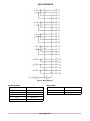
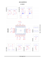
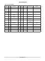
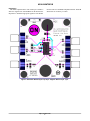
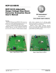
NS3L500MTGEVB
3.3V, 8-Channel, 2:1 Gigabit
Ethernet LAN Switch with
LED Switch Evaluation
Board User's Manual
http://onsemi.com
EVAL BOARD USER’S MANUAL
Overview
The NS3L500 evaluation board has been designed for a
quick evaluation of the NS3L500. Among its main
characteristics, this evaluation board has been constructed to
easily interface with a customer’s systems and equipment
through SMA connectors. This document provides a bill of
materials, board schematic, and a layout overview of the
evaluation board. The appropriate lab test setups are also
provided.
This document should be used with the NS3L500
datasheet available on www.onsemi.com. The datasheet
contains full technical details about the NS3L500
specifications and operation. The evaluation board is
implemented in four metal layers with 50 W characteristic
impedance. The PCB dimensions are 50mm by 57.6 mm.
The NS3L500 is an 8−channel 2:1 LAN switch with 3
additional built−in SPDT switches for LED routing. This
switch is ideal for Gigabit LAN applications due to its low
ON−state resistance and capacitance giving the switch a
typical bandwidth of 800 MHz. The switch also has
excellent ON−state resistance match, low bit−to−bit skew,
and low crosstalk among channels. The switch is
bidirectional and offers little or no attenuation of the
high−speed signals at the outputs.
This part can be used to replace mechanical relays in
low−voltage LAN applications that interface a physical
layer over CAT 5 or CAT 6 unshielded twisted pair cable
through an isolation transformer. The NS3L500 is available
in a 56−pin WQFN package and operates over the extended
*40°C to +85°C temperature range.
Figure 1. NS3L500 Evaluation Board Photo
© Semiconductor Components Industries, LLC, 2012
June, 2012 − Rev. 2
1
Publication Order Number
EVBUM2122/D
NS3L500MTGEVB
Figure 2. Block Diagram
PIN DESCRIPTION
TRUTH TABLE
Pin Name
Description
SEL
Function
Ax
Data I/Os
L
Ax to xB1: LEDx to xLED1
H
Ax to xB2: LEDx to xLED2
xBy
Data I/Os
SEL
Select Input
LEDx
LED I/O Port
xLEDy
LED I/O Port
http://onsemi.com
2
NS3L500MTGEVB
Equipment
The following table details the equipment used in the context of this application note manual:
Table 1. EQUIPMENT
Description
Quantity
Regulated DC Power Supply
1
Banana Cable
2
Oscilloscope with SMA Adapters
1
Differential Waveform Generator
1
SMA Cable
2−3
Get Started…
III. To observe switching of the LED I/O channels:
1. LED0 can be connected directly to VCC or to the
function generator. If using the function generator,
use an SMA cable to connect the function
generator to LED0, which has been set up as the
LED input channel. Set the function generator to
the desired pulse frequency from 0 to VCC.
2. Move the jumper at J5 to change the logic level of
SEL in order to switch between 0LED1 and
0LED2. Observe the switching of the LEDs at D1
and D2. The outputs should not be connected to
the oscilloscope.
3. In order to observe LED channel switching on an
oscilloscope, remove diodes at D1 and D2 and
series resistors at D6 and D8. Solder 0 W resistors
at D6 and D8. The LED channels can now be
tested in the same manner as the data I/O channels
in the previous section.
I. Set the power supply to 3.3 V. Connect the power supply
to VCC and GND on the board using the banana cables. The
supply current should be less than 1 mA.
II. To observe the switching of the data I/O channels:
1. Use an SMA cable to connect the function
generator to A3. Adjust the internal impedance of
the waveform generator 50 ohms. Set the desired
bit rate up to 1 Gbps (1000BASE-T) and
amplitude up to 3 Vpp per differential channel. Set
the frequency and pattern to a 1 Gbps square wave
(1000BASE−T). Do not turn on the generator until
the load has been connected.
2. Connect channels 3B1 and 3B2 to the oscilloscope
through single-ended 50 W probes.
3. Turn on the generator.
4. Move the jumper at J5 to change the logic level of
SEL in order to switch between 3B1 and 3B2.
http://onsemi.com
3
NS3L500MTGEVB
Figure 3. Board Schematic
SCHEMATIC
http://onsemi.com
4
NS3L500MTGEVB
Table 2. BILL OF MATERIALS
Designator
Qty
Description
Value
Tolerance
Footprint
Manufacturer
Manufacturer Part
Number
C1
1
Ceramic Capacitor SMD
1 mF
10%
805
TDK Corporation
C2012Y5V1C105Z/0.85
C2, C3, C4,
C5, C6, C7,
C8
7
Ceramic Capacitor SMD
0.1 mF
10%
603
Yageo
CC0603ZRY5V7BB104
D1, D2
2
LED
n/a
n/a
0603/0805
Panasonic
LNJ326W83RA
R1, R3, R4,
R5, R7
5
Do not populate
n/a
n/a
n/a
n/a
n/a
R2
1
0.2W Surface Mount
Resistor
51
1%
603
Rohm
Semiconductor
ESR03EZPF51R0
R6, R8
2
0.125W Surface Mount
Resistor
392
1%
603
Stackpole
Electronics Inc
RNCP 0603 T1 392 1% R
J1, J2
2
Banana Connector
n/a
n/a
7mm Hole
Johnson
Components
111−2223−001
J3, J4, J6,
J7, J8, J9
6
SMA Connector
n/a
n/a
n/a
Emerson Network
Power Connectivity
Solutions
142−0711−821
J10, J11,
J12, J13
4
Standoff Nut
n/a
n/a
n/a
Keystone Electronics
1903C
J10, J11,
J12, J13
4
Standoff Screw
n/a
n/a
n/a
Keystone Electronics
4814K−ND
J5
1
3−pin Header
n/a
n/a
Header3
Tyco Electronics
5−826629−0
J5
1
2−pin Jumper
n/a
n/a
n/a
3M
969102−0000−DA
TP1
1
PCB Shorting Link
n/a
n/a
n/a
Harwin
D3082−46
U1
1
NS3L500
n/a
n/a
WQFN56
5x11, 0.5P
ON Semiconductor
NS3L500MTTWGTAG
http://onsemi.com
5
NS3L500MTGEVB
PCB Design
The PCB is implemented in four metal layers and FR−4
dielectric. Signal traces on the PCB have 50 W characteristic
impedance to minimize high speed signal loss. The PCB is
made of lead−free and RoHS compliant materials. The PCB
dimensions are 50 mm by 57.6 mm.
Figure 4. Evaluation Board Layout. Top layer: magenta. Bottom layer: cyan.
http://onsemi.com
6
NS3L500MTGEVB
Electrical Layout Considerations
• The ground plane of the PCB will be used to determine
Implementing a high speed switch device requires careful
PCB design to preserve signal integrity. The evaluation
board serves as a layout example and can support the design
engineers to preserve high speed performances.
Electrical layout guidelines:
• The bypass capacitor must be placed as close as
possible to the Vcc input pin for noise immunity.
• The characteristic impedance of each segment must be
50 W single-ended and 100 W differential according to
IEEE standard 802.3.
the characteristic impedance of each line.
• All corresponding differential A+/− line segment pairs
must be the same length.
• The use of vias to route these signals should be avoided
•
when possible.
The use of turns or bends to route these signals should
be avoided when possible. When bends are needed, use
45° bends instead of 90° bends.
ON Semiconductor and
are registered trademarks of Semiconductor Components Industries, LLC (SCILLC). SCILLC owns the rights to a number of patents, trademarks,
copyrights, trade secrets, and other intellectual property. A listing of SCILLC’s product/patent coverage may be accessed at www.onsemi.com/site/pdf/Patent−Marking.pdf. SCILLC
reserves the right to make changes without further notice to any products herein. SCILLC makes no warranty, representation or guarantee regarding the suitability of its products for any
particular purpose, nor does SCILLC assume any liability arising out of the application or use of any product or circuit, and specifically disclaims any and all liability, including without
limitation special, consequential or incidental damages. “Typical” parameters which may be provided in SCILLC data sheets and/or specifications can and do vary in different applications
and actual performance may vary over time. All operating parameters, including “Typicals” must be validated for each customer application by customer’s technical experts. SCILLC
does not convey any license under its patent rights nor the rights of others. SCILLC products are not designed, intended, or authorized for use as components in systems intended for
surgical implant into the body, or other applications intended to support or sustain life, or for any other application in which the failure of the SCILLC product could create a situation where
personal injury or death may occur. Should Buyer purchase or use SCILLC products for any such unintended or unauthorized application, Buyer shall indemnify and hold SCILLC and
its officers, employees, subsidiaries, affiliates, and distributors harmless against all claims, costs, damages, and expenses, and reasonable attorney fees arising out of, directly or indirectly,
any claim of personal injury or death associated with such unintended or unauthorized use, even if such claim alleges that SCILLC was negligent regarding the design or manufacture
of the part. SCILLC is an Equal Opportunity/Affirmative Action Employer. This literature is subject to all applicable copyright laws and is not for resale in any manner.
PUBLICATION ORDERING INFORMATION
LITERATURE FULFILLMENT:
Literature Distribution Center for ON Semiconductor
P.O. Box 5163, Denver, Colorado 80217 USA
Phone: 303−675−2175 or 800−344−3860 Toll Free USA/Canada
Fax: 303−675−2176 or 800−344−3867 Toll Free USA/Canada
Email: [email protected]
N. American Technical Support: 800−282−9855 Toll Free
USA/Canada
Europe, Middle East and Africa Technical Support:
Phone: 421 33 790 2910
Japan Customer Focus Center
Phone: 81−3−5817−1050
http://onsemi.com
7
ON Semiconductor Website: www.onsemi.com
Order Literature: http://www.onsemi.com/orderlit
For additional information, please contact your local
Sales Representative
EVBUM2122/D