1
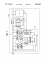
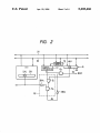
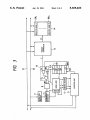
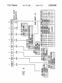
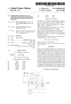
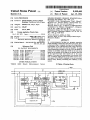
USOO530546OA
United States Patent [19]
[11]
[45]
Kaneko et a1.
[54] DATA PROCESSOR
[75] Inventors: Susumu Kaneko, Kodaira; Keiichi
Kurakazu, Tachikawa, both of Japan
[73] Assignee: Hitachi, Ltd., Tokyo, Japan
[21] Appl. No.: 254,267
[22] Filed:
[30]
[51]
[52]
Japan .................................... ., 255180
364/232.8; 364/232.9; 364/245.7; 364/245.8;
364/246.9
364/200 MS File, 900 MS File;
395/775, 575, 425
References Cited
U.S. PATENT DOCUMENTS
Re. 28,109
3,828,327
4,393,459
8/1974 Provenzano et a1. ............. .. 364/900
8/1974 Berglund et a]. ......... ..
364/200
7/1983 Huntley et a]. .
4,519,032 5/1985
4,628,448 12/1986
Mendel] .... ..
Murao ............... ..
364/900
395/725
364/200
4,783,731 11/1988 Miyazaki et a1.
364/200
4,825,358
364/200
4/1989
Letwin .............. ..
4,887,204 12/1989 Johnson et a1. ...............
68000
Hitachi
Microcomputer
IBM Technical Disclosure Bulletin, vol. 28, No. 10,
Mar. 1986, PP- 4538-4539.
Primary Examiner—Debra A. Chun
Attorney, Agent, or Firm-Fay, Sharpe, Beall, Fagan,
Minnich & McKee
[57]
ABSTRACT
In a microcomputer having two program execution
states including a supervisor state and a user state, there
is disposed a flag or a register having such a flag indicat
ing whether or not a RAM area used in the supervisor
state can be used in the user state by the CPU. A judge
circuit determines whether or not the CPU has made an
attempt to invalidly access the RAM in the user state
based on the content of the ?ag or the register and that
of the supervisor/user state specify bit in the status
register. In a case of an occurrence of an access viola
tion, a violation signal is sent to the CPU and the selec
tion signal of the RAM is disabled (to be set to an inef
364/200
fective state), thereby increasing the reliability of the
system.
System
30 Claims, 4 Drawing Sheets
OTHER PUBLICATIONS
“HMCS
Motorola Inc., Second Edition, Prentice-Hall Inc.,
1985, pp. l-l, l-2, l-4, 6-1, 6-2, and 6-3.
Borivoje Furht, et al., “A Survey of Microprocessor
“Protection Scheme for Non-Key Storage Systems”,
Int. Cl; ....................... .. G06F 9/00; G06F 12/14
us. 01. ........................... .. 395/775; 364/DIG. 1;
[56]
HD68000, HD68000Y, HD68000P, HD68000PS Micro
Processing Unit (MPU)”, Sep, 1984, p. 52.
_“MC68020 32-Bit Microprocessor User’s Manual”,
vol. 20, No. 3, Mar. 1987, pp. 48-67.
Foreign Application Priority Data
[58] Field of Search
Apr. 19, 1994
Architecture for Memory Management”, Computer,
Oct. 5, 1988
Oct. 9, 1987 [JP]
5,305,460
Patent Number:
Date of Patent:
/ MCU
I
3
msmucnou
REGISTER
It
MICRO -ROM
5
comm orconea
EXECUTION UNlT
US. Patent
Apr. 19, 1994
Sheet 2 of 4
FIG. 2
CPU
S/U SR
ADDRESS
COMPARATOR
~17 G3
5,305,460
1
5,305,460
2
is sent to the CPU and a selection signal of the RAM is
DATA PROCESSOR
disabled (is set to the invalid state).
According to the means above, in a case where it is
BACKGROUND OF THE INVENTION
The present invention relates to a data processing
desired that the CPU uses the RAM in the supervisor
state in order to keep the data protected in the RAM, a
state preventing an access is set to the new flag or regis
ter thus disposed. This automatically prevents an access
technology, and in particular, to a technology that is
particularly effective when applied to a data processor
having a higher operation mode and a lower operation
mode, for example, to a technology effectively applied
to the associated RAM in the user state so as to prevent
destruction or a read operation of important data; or, so
that a restoration of data destroyed by an exception
to a control method of a memory in a microcomputer.
Conventionally, a processor may have two program
processing or the like is enabled, thereby achieving the
objects above to improve the reliability of the system.
state and an operation mode called a user state, where
Above and other objects and novel features of the
the processor is capable of operating either of the two
present
invention will become apparent from the fol
states. For example, microprocessors similar to the 16 5 lowing detailed description taken in conjunction with
bit microprocessor HD68000 of Hitachi Ltd. operate in
the accompanying drawings.
execution states, an operation mode called a supervisor
this manner. (For details refer to page 52 of the “HMCS
68000 Hitachi Microcomputer System HD68000,
BRIEF DESCRIPTION OF THE DRAWINGS
FIG. 1 is a block diagram schematically showing a
HD68000Y, HD6800PHD, HD68000PS Micro Pro
cessing Unit (MPU)".)
?rst embodiment in a case where the present invention
The supervisor state is a higher state of the processor
program execution states and the central processing
is applied to a microprocessor;
FIG. 2 is a block diagram schematically showing a
unit (CPU) can use any instructions and can access any
registers in this state. The user state is a lower state of
the program execution states and the CPU is not al
second embodiment in a case where the present inven
tion is applied to a microprocessor;
FIG. 3 is a block diagram schematically showing the
lowed to use the instructions and registers which
third embodiment in a case where the present invention
greatly affect the system in this state. Namely, in the
supervisor state, the CPU can execute a predetermined
instruction which the CPU cannot execute in the user
state.
is applied to the microprocessor, and
FIG. 4 is a con?guration diagram showing a bit con
3O ?guration example of a bank mode register including an
access level specify bit of the integrated RAM.
As described above, with the provision of two pro
gram execution states, the microprocessor can more
DESCRIPTION OF THE PREFERRED
EMBODIMENTS
efficiently execute a multitask processing and the like.
Incidentally, in microcomputers having the two pro
gram execution states as described above, a bit is ordi 35
narily disposed in a status register of the CPU for the
purpose of indicating whether the processor is in the
FIG. 1 shows an embodiment in which the present
invention is applied to a microprocessor having an inte
grated RAM.
supervisor state or the user state. This would be used to
Although not particularly limited to, each circuit
indicate the current program execution state.
block enclosed with dot-and-dash lines in FIG. 1 is
However, in the case where for example, a data ac 40 formed on a single semiconductor chip such as a mono
cess device such as a RAM is integrated in a micro
crystalline silicon substrate.
processor having the two program execution states, the
following problem may arise. Where a CPU uses the
integrated RAM as the data area while in the supervisor
state, it is feared that in some cases important data may 45
be destroyed if the CPU mistakenly accesses this data
area while in the user state.
The microprocessor of this embodiment is provided
with a central processing unit (CPU) operating accord
ing to the microprogram control method. The central
processing unit has a micro read only memory (ROM) 1
in which a microprogram is stored and the micro ROM
is accessed from a microaddress decoder 2 so as to
sequentially read out microinstructions constituting the
SUMMARY OF THE INVENTION
microprogram.
It is therefore an object of the present invention to 50 The microaddress decoder 2 is supplied with an ad
prevent a microcomputer having two program execu
dress signal generated by a microaddress generate cir
tion states, which includes the supervisor state and the
user state, an invalid access to, for example, a RAM area
used in the supervisor state. This prevents the RAM
from being mistakenly affected and prevents the de
struction of important data, thereby improving the reli
ability of the system.
The representative features of the present invention
disclosed in this speci?cation are as follows.
Disposed in the processor is a ?ag or a register to
indicate whether or not a RAM area used by the CPU
in the supervisor state is to be accessed in the user state.
Also disposed is a judge circuit and based on the con
tent of the ?ag or register and on the content of the bit
cuit 4 based on an operation code of a microinstruction
fetched into an instruction register 3, and when the
55 address signal is decoded, a ?rst instruction is read out
of a group of microinstructions in a sequence executing
the macro instruction. Of this group of microinstruc
tions corresponding in sequence to the macroinstruc
tion, the second and subsequent microinstructions are
read out, based upon the next address from the previous
microinstruction and the address supplied from the
microaddress generate circuit 4 occurring when a code
of the next address field of the previously read out mi
croinstruction is supplied to the microaddress decoder
indicating the supervisor/user state in a status register, 65 2. The microinstructions thus read out are then decoded
by a control decoder 5, thereby generating control
signals for an execution unit 6 and the like including
has effected an invalid access to the RAM in the user
state. In a case of an access violation, a violation signal
various registers and an arithmetic logic unit (ALU).
the judge circuit determines whether or not the CPU
3
5,305,460
4
the coincidence signal C at a high level is delivered
from the address compare circuit 17, the output from
the AND gate G1 is set to the high level. As a result, the
output of the AND gate 6;, where the input is a signal
In the CPU, there is disposed a group 7 of control
registers including a status register SR indicating the
internal control state, a condition code register CCR,
program counter PC, a system stack pointer SSP, and
I/O base register IBR enabling a group of the control
obtained by inverting the state signal of the bit S/U, is
changed to the high level. The output signal is supplied
registers above to be reallocatable in the address space
of the CPU, an exception vector base register EBR for
establishing relocatability of a vector for an exception
processing in the CPU address space, and the like.
to an access violation signal AV to the exception pro
cessing circuit 8 of the CPU.
As a result, the CPU recognizes that the integrated
RAM is invalidly accessed and then controls the mi
Moreover, an integrated RAM 11 is used as work
areas of the CPU including a temporary storage area of
croaddress generate circuit 4 to call, for example, a trap
data and a stack area. A memory control circuit 12 is
routine from the micro ROM 1 or passing control to an
formed on the same chip for providing a refresh con
associated exception processing, for example, thereby
trol, a chip selection control, and a wait state control.
reading from an external memory a program to restore
These circuits and the CPU are connected to each other 15 the data in the vector address method and to return to
via an address bus 21 and a data bus 22.
the state prior to the access. If the microprocessor pos
In the microcomputer of this embodiment, there is
sesses an integrated ROM, the program to restore the
disposed an address setting register 16 for setting an
data may be stored in the integrated ROM.
address space in which the integrated RAM 11 is to be
Incidentally, the exception processing circuit 8 is
allocated. An address compare circuit 17 compares an 20 con?gured so as to be supplied with a signal from the bit
address on the address bus 21 with an address set to the
S/U in the status register SR for indicating the super
address setting register 16 so as to determine whether or
visor/user state such that an exception processing for a
not the address generated by the CPU is to be used to
privilege violation other than that described above can
access the integrated RAM. Also provided is an access
also be executed.
level judge circuit 13 comprising an AND gate G1 and
In this fashion, in the embodiment above, the state of
an AND gate 6;. The input signals of the AND gate
the status signal of the access level specify bit ALV of
6] include a coincidence signal C outputted from the
the control register RCR] and that of the signal of the
address compare circuit 17. Input signals to the AND
bit S/U in the status register SR for indicating the
gate G2 include a signal obtained by inverting through
supervisor/user state, determine whether or not the
an invertor INVI a state signal of the bit S/U indicating
integrated RAM 11 is accessible and is discriminated so
the supervisor/user state of the status register SR in the
as to generate an access violation signal.
CPU and an output signal from the AND gate 6].
Table 1 shows the accessibility of the integrated
Incidentally, "0” of the bit S/U indicates the user state,
RAM in the case above.
whereas “1" indicates the supervisor state. In addition,
the coincidence signal C delivered from the address
TABLE 1
compare circuit 17 is supplied as a selection signal CS
Access level of
CPU execution state gS/U bit}
for selecting the integrated RAM 11.
In addition, although not particularly limited to,
integrated RAM
User state
Supervisor state
‘
x
'
'
User level allowed
User level not allowed
there is disposed in the memory control circuit 12 a
plurality of control registers RCR] to RCRn including
a bank mode register and a refresh control register each
supplied with an address. Of these registers, a bit of the
40
'2 Accessible
x: Not accessible
In consequence, when it is desired that the CPU uses
register RCR1 accessible only in the supervisor state is
the integrated RAM in the supervisor state and keeps
employed as a bit ALV indicating whether or not the
integrated RAM is accessible in the user state. The state 45 the data therein, “1" need only be set to the access level
specify bit ALV in the control register RCR before the
signal of this bit ALV is supplied to the other input
terminal of the AND gate 6] constituting the access
level judge circuit 13. Although not particularly limited
mode is changed to the user state. As a result of this
to, when the access level specify bit ALV is “0”, a state
in which the RAM is accessible as indicated; whereas
when the bit ALV contains “1", it is indicated that the
RAM is not accessible.
In the memory control circuit 12, there is provided a
the integrated RAM is unnecessary, only by setting the
operation, when the integrated RAM is used in the user
state, a condition that the RAM is invalidly accessed
can be recognized. 0n the other hand, when the data in
access level specify bit ALV to "0" can the integrated
RAM be freely used in the user state. This enables the
decoder for decoding an address outputted from the
integrated RAM, even if the capacity thereof is small, to
CPU onto the address bus 21 so as to select one of the
be effectively used. However, in place of the operation
control registers RCR] to RCRn. The system is con?g
to supply the access violation signal AV to the microad~
dress generate circuit 4, a bit may be disposed to indi
ured such that a bit of a specified control register can be
set via the data bus 22. In addition, according to this
embodiment, successive addresses are assigned to the
registers RCR] and RCR,I in order that these registers
cate whether or not a violation exists in a register of the
group 7 of control registers of the CPU so as to set “1"
to the pertinent register.
Incidentally, such as the address setting register 16,
may be easily reallocated in the address space by use of
there may be disposed a register specifying a partial area
the I/O base register IBR.
of the integrated RAM 11, in addition to the address
In consequence, in the microprocessor of this em
designation of an address space of the integrated RAM
bodiment, when the access level specify bit ALV in the
control register RCR1, is set to "l” and the bit 8/!) of 65 11. As a result, access can be inhibited in the user state
to only the area used in a case where the area to be used
the status register in the CPU is “0" indicating the user
in the supervisor state is a portion of the integrated
state, an address in theladdress space of the integrated
RAM 11. According to the embodiment above, al
RAM 11 is outputted to the address bus 21, and when
5
5,305,460
6
though the access level specify bit ALV is located in the
control register RCR of the control circuit 12, the pres
ent invention is not limited to that embodiment; namely,
register group 14, coincidence detection signal C is to
be supplied from the memory control circuit 12 and the
AND gate G1 of the access level judge circuit 13. More
a ?ag or a register dedicated for the purpose of access
over, in this embodiment, if an address coincidence is
inhibition may be provided.
detected when the ALV bit is “l”, the selection signal
The register may be positioned at an outside or inside
location with respect to the CPU; furthermore, a free
bit of a status register or a control register in the CPU
may also be used.
’ Moreover, by con?guring the register with the access H 0
level specify bit such that the register can be set to the
group 14 is not to be changed to the selection level.
As a result, in this embodiment, by setting “1” to the
access level specify bit ALV in the bank mode register
CS for selecting the RAM constituting the register
BMR by use of a dedicated instruction, an access to a
register bank used in the supervisor state can be inhib
reset or set state in response to a reset signal R, an in
ited in the user state, thereby smoothly and safely effect
valid access to the integrated RAM attempted prior to
an initialization and immediately after the power is
ing the change-over of the multitask processing.
turned on can be prevented.
FIG. 4 shows a configuration example of the bank
15 mode register provided with an access level specify bit
FIG. 2 shows the second embodiment of a micro
processor according to the present invention.
In the microprocessor of this embodiment there is
associate with the RAM.
The bank mode register BMR of this embodiment
includes eight bits comprising a RAM enable control bit
disposed a new register 18 having the access level spec
RAME, a bank permit mode specify bit BPM, an inter
ify bit ALV; in addition, by using the access violation
nal RAM access level specify bit ALV according to the
signal AV outputted from the access level judge circuit
present invention, a bank mode specify bit BMD, a
13 con?gured in the same fashion as that of the embodi
system stop mode specify bit SSTOP, a bus retry enable
ment of FIG. 1, the selection signal CS supplied to the
control bit BRTE, and bank select bits SLCT 1 and
integrated RAM 11 is forcibly negated so as to inhibit
SLCTO.
the access itself to the RAM 11.
25
Among these bits, when the RAM enable control bit
That is, there is disposed an AND gate G3 of which
RAME is set to “1”, the integrated RAM is enabled to
the input signals include the address coincidence signal
be effective; whereas, when RAME is cleared to “O”,
C delivered from the address compare circuit 17 and a
the integrated RAM as a memory is set to be ineffective.
signal attained by inverting through an invertor INVZ
In this situation, if an access is issued to a data area of
the access violation signal AV outputted from the ac
cess level judge circuit 13 such that an output from this
gate G3 is supplied as a selection signal CS to the inte
the integrated RAM by use of an address thereof, the
, grated RAM 11.
In consequence, according to this embodiment, if “1”
is set to the ALV bit of the control register 18, even
when an address in the address space of the RAM 11 is
outputted to the address bus 21, an access to the inte
grated RAM 11 is not accomplished. As a result, the
data in the RAM 1 used in the supervisor state can be
protected.
FIG. 3 shows the third embodiment of a micro
processor according to the present invention.
In the embodiment above, description has been given
same address of an external device is to be accessed.
In addition, the bank permit mode specify bit BPM is
disposed to determine whether or not a portion of the
integrated RAM associated with the register bank area
of the CPU can be accessed as a memory. When the bit
BPM is set to “1”, this area above can be accessed as a
memory; whereas, when the bit BPM is cleared to “O”,
the area cannot be accessed as a memory. When a read
operation is accomplished on this area in a case of BPM
0, all bits are attained as unde?ned bits; whereas, even
when a write operation is attempted thereon, the RAM
is not in?uenced with the write operation and the value
stored therein is kept unchanged.
of a case where the integrated RAM assigned as a work
Incidentally, the bit BPM is effective when “l” is set
area of the CPU cannot be used in the user state; 45 to the bit RAME. If the bit RAME is cleared to “0”, an
whereas, in this third embodiment, in a case where a
external device is accessed regardless of whether the bit
register bank employed in a multitask processing com
BPM is “1” or “O”
prises the RAM, the register bank is set so as to be used
The system stop mode specify bit SSTOP is used to
or not to be used in the user state. That is, a group 14 of
select a low consumption power state of the CPU when
general-purpose registers comprising the RAM pos
a particular instruction called a SLEEP is executed. If a
sesses 16 register banks BN0 to BN15, each including 16
registers, and there is disposed a register bank number
specify bit for specifying one of the register banks BN0
to BN15 and a bank mode register BMR supervising a
change-over bit and the like of the register banks as one
of the control registers in the register group 7. More~
over, a bit of the bank mode register BMR is employed
SLEEP instruction is executed when the bit SSTOP is
as the access level specify bit ALV such that the state
“0”, the system enters the sleep mode in which only the
operation of the CPU is stopped-with the operations of
the peripheral devices remaining unchanged. On the
other hand, if the SLEEP instruction is executed when
the bit SSTOP is set to "1”, the system is set to the
system stop mode in which the operations of the CPU
and peripheral devices except the refresh controller of
the integrated RAM are stopped. Incidentally, in the
signal of this bit ALV is inputted to the AND gate G]
of the access level judge circuit 13 con?gured in the 60 sleep mode, the CPU is initiated again only in response
same fashion as that of the embodiment of FIG. 1.
to an interruption from a peripheral device or an exter
In addition, according to this embodiment, the ad
dress setting register 16 and the address compare circuit
nal device; whereas, in the system mode, the CPU is
reactivated only in response to an external interruption.
The bus retry enable control bit BRTE is employed
ory control circuit 12 effecting the selection control of 65 to specify a countermeasure procedure to be effected
the general-purpose register group 14 and the control
when a bus error takes place. When the bit BRTE is
register group 7. When the address on the address bus
cleared to “0”, the system enters the bus error mode in
21 is within the address range of the general purpose
which the bus error exception processing sequence is
17 of the embodiment of FIG. 1 are located in the mem
7
5,305,460
8
In addition, with reference to the embodiment above,
description has been given of a prevention of the data
achieved; whereas, when the bit BRTE is set to “l”, the
bus retry mode is set so as to effect the same bus cycle
again.
destruction in the integrated RAM; however, the pro
In addition, the bank mode specify bit DMD is dis
posed to specify a utilization of the register banks of the
integrated RAM together with the bank select bits
tection of secrecy of the ROM data can be effected by
applying the present invention to a read only memory
(ROM), integrated in the microprocessor, a program
mable ROM (PROM), an erasable PROM (EPROM) of
SLCTI and SLCTO. When the bit BMD is cleared to
which data is erasable by means of an ultraviolet ray, an
“0", the system enters the global mode in which only
electrically erasable EPPROM (EEPROM) of which
one of a plurality of register banks can be used; whereas
when the bit BMD is set to “I”, one half of the inte 0 data is electrically writable and erasable, and the like.
In addition, the RAM as an object of the control
above need not be limited to the integrated RAM,
namely an external RAM is also applicable.
Moreover, in place of the provision of the access
level specify bit ALV in the control register, the bit
grated RAM is used as eight global banks and the re
maining half thereof is employed such that the RAM
provides an in?nite number of successive banks. Inci
dentally, in any mode above, for the global banks, the
bank number register can be rewritten by use of a dedi
may be disposed as a ?ag.
According to the present invention, there are attained
cated bank switch instruction when an interruption
takes place, thereby effecting switching or changeover
operation between global banks.
the following effects.
There is disposed a ?ag or a register to indicate
whether or not a RAM area used by the CPU in the
supervisor state can be used in the user state. Also dis
Furthermore, the bank selects bits SLCTl and
SLCTO can be used to change the configuration of the
banks according to the combination of SLCTl and
SLCTO in the global mode in which the bank mode
specify bit BMD is “0". That is, when SLCTl and
SLCTO are “0, 0”; “0, 1”; “l, O”; and, "l, I"; there are
established the 2-bank, 4-bank, S-bank, and l6-bank
posed is a judge circuit for determining based on the
content of the ?ag or register and also based on the
supervisor/user state indication bit of the status register
whether or not the CPU has attempted an invalid access
to the RAM in the user state. When an access violation
configurations, respectively.
occurs, a violation signal is set to the CPU and a selec
Incidentally, as in the case of the embodiment of FIG.
tion signal of the RAM is negated (is set to the invalid
1, the access violation signal AV outputted from the
access level judge circuit 13 may be supplied to the
state). Consequently, in a case where the CPU uses the
RAM in the supervisor state and the data is desired to
CPU 1 to notify the access level violation to the CPUl,
thereby effecting the restoration thereof and the coun
be kept therein, by setting a state inhibiting the access to
the new flag or register thus disposed, an access to the
corresponding RAM in the user state is automatically
inhibited. Through this operation, destruction or a read
termeasurement processing.
Furthermore, according to the embodiment above, in
a case where an access violation is detected, the condi
tion is noti?ed to the CPU so as to return to the original
state through an exception processing or an access to
out operation of important data can be prevented and
the data destroyed by an exception processing or the
the integrated RAM itself is inhibited; however, there
reliability of the system is greatly improved.
like can be restored._ This leads to an effect that the
may be disposed an access inhibit bit in the control
register RCR], the control register 18, or other register
40
such that whether the access to the RAM is inhibited or
the data is to be restored after the invalid access can be
selected when an access violation takes place. In addi
A concrete description has been given of the inven
tion accomplished by the present inventor with refer
ence to the embodiments; however, the present inven
tion is not limited by those embodiments. It is to be
appreciated that the embodiments can be changed and
tion, it is also possible in this situation to dispose a read/
modified without departing from the scope and spirit of
write specify bit such that a read access is allowed and 45 the present invention. For example, in the embodiments
only a write access is inhibited depending on the setting
above, there is disposed a register or ?ag indicating the
of the read/write specify bit.
access level of the RAM such that depending on the
In addition, in a case where there is con?gured a
state thereof, the integrated RAM can be used only in
microprocessor not having a function in which the
the supervisor state or in the supervisor and user states;
allocation address of the integrated RAM 11 can be
however, there may be disposed two integrated RAMs
freely reallocated in the address space possessed by the
each having the same address space such that depending
microprocessor, the address compare circuit 17 can be
on the content of the register designating the access
replaced with a decode circuit having a relatively sim
level, either one of the RAMs is set to be accessible so
ple circuit con?guration. The address compare circuit
as to prevent an access in the user state to the RAM
17 compares the address on the address bus 21 with the
used in the supervisor state, thereby protecting the data
in the RAM. However, when the integrated RAM is
allocation address of the integrated RAM 11 and is
hence completely operable even if the allocation ad
dress is ?xed, the same function can be possessed with a
decode circuit having a smaller circuit size.
Incidentally, according to the embodiment above, 60
there is disposed a register or a flag to which the access
level of the integrated RAM is set so as to enable the
control to be effected by means of the program; how
ever, for example if there is a margin in the number of
pins of the microprocessor, there may be disposed a
terminal to set the access level from an external device,
thereby enabling the hardware control to be achieved
by the external circuit.
shared between the supervisor and user states like in the
case of the embodiment, a higher utilization rate of the
memory is developed.
In addition, according to the embodiment above,
when an access violation with respect to the integrated
RAM is detected, the access is inhibited or a restoration
of the data is effected; however, the present invention is
also applicable to a case where the CPU simply wants to
know whether or not the user has referenced the inte
grated RAM.
Furthermore, although the description has been
given of a memory access violation and the counter
9
5,305,460
measurement processing thereof in conjunction with
the embodiment, the present invention is also applicable
10
mode and the user mode, the microcomputer compris
mg:
a register having a bit for indicating whether the
to a case where the access in the user state is to be
inhibited with respect to the peripheral I/O devices
other than the memory, for example, a particular I/O
central processing unit can access a memory in the
user mode, the bit of the register being rewriteable
by the central processing unit, when the central
port.
processing unit operates in the supervisor mode,
The description above is associated with cases where
the invention primarily accomplished by the present
wherein the central processing unit executes a pro
inventor is applied to a microprocessor as a utilization
cess to return to the operation state prior to access
?eld as the background of the invention; however, the
present invention is not restricted by those cases, but
can be utilized in a single-chip microcomputer compris
ing a timer, a serial communication circuit, DMA con
troller, and the like disposed on the same chip, a mi
of the memory, if the memory is accessed by the
central processing unit when the bit of the state
crocomputer of a board type, and a general data proces
unit is restricted from use of the memory in the user
mode.
register is indicating that the central processing
unit is operating in the user mode and the bit of the
register is indicating that the central processing
sor having a function associated with a data access.
5. The microcomputer in accordance with claim 4
wherein said register is con?gured so as the bit of said
register is set to indicate whether the central processing
What is claimed is:
1. A microcomputer formed on a single semiconduc
tor chip comprising a central processing unit which
operates in either a supervisor mode which is permitted 20 unit can access the memory while in the user mode,
through an instruction available only in said supervisor
to execute all instructions of the microcomputer or a
mode.
6. The microcomputer in accordance with claim 4
user mode which is limited in the instructions it is per
mitted to execute, and which includes a status register
having a bit for indicating the mode in which the central
processing unit is operating, the microcomputer com
further including:
25
prising:
memory means for storing data; and
a register having a bit for indicating whether the
‘
an address register for allocating address space to the
memory.
7. The microcomputer in accordance with claim 6
further comprising:
means in the user mode, the bit of the register being
a comparator means for comparing an address of the
address register and an address located on an ad
rewriteable by the central processing unit, when
the central processing unit operates in the supervi
dress bus of the microcomputer; and
an outputting means for outputting a resultant signal
central processing unit can access the memory
of the comparison.
8. The microcomputer in accordance with claim 7,
accessing the memory means when the bit of the 35 further comprising access level judge means for judg
ing, in accordance with contents of the bits of the state
status register indicates that the central processing
sor mode,
wherein the central processing unit is restricted from
unit is operating in the user mode, and the bit of the
register indicates that the central processing unit is
restricted from using the memory means in the user
mode and wherein the central processing unit ac
cesses the memory means regardless of the bit of
the register when the bit of the status register indi
cates that the central processing unit is operating in
the supervisor mode.
2. The microcomputer in accordance with claim 1 45
further including a microprocessor in which said status
register is disposed.
3. The microcomputer in accordance with claim 2,
further comprising access level judge means for judging
register and the register, whether to return to an opera
tion state existing prior to an access of the memory,
wherein the access level judge means provides a sig
nal for the central processing unit to execute a
process to return to the operation state existing
prior to the access of the memory when the bit of
the state register indicates the central processing
unit is operating in the user mode and the bit of the
register indicates that the central processing unit is
restricted from use of the memory in the user
mode.
9. The microcomputer in accordance with claim 8
wherein when the signal indicating the central process
whether access is to be made to the memory in accor 50 ing unit is restricted from access to the memory is out
dance with the bits of the status register and the register,
wherein the access level judge means provides a sig
putted from said access level judge means, a selection
signal of said memory is set to an invalid state.
10. The microcomputer in accordance with claim 8
nal to the central processing indicating that the
wherein when the signal indicating that the central
central processing unit cannot access the memory
when the bit of the status register is indicating that 55 processing unit cannot access the memory is outputted,
the central processing unit is operating in the user
by said access level judge means, a selection signal of
said memory is set to an invalid state.
mode and the bit of the register is indicating that
11. The microcomputer in accordance with claim 1,
the central processing unit cannot use the RAM
further comprising access level judge means for judging
module in the user mode.
4. A microcomputer formed on a single semiconduc 60 whether a return to an operation state prior to access of
the memory in accordance with contents of the bits of
tor chip comprising a central processing unit which
operates in either a supervisor mode in which all given
instructions and internal registers of the microcomputer
the state register and the register and the resultant signal
of the comparator means,
re?ects an operation state thereof, wherein the state
wherein the access level judge means provides a sig
nal for the central processing unit to execute a
process to return to the operation state existing
prior to access of the memory, when the status
register has a bit for indicating one of the supervisor
register indicates the central processing unit is op
can be used or a user mode in which particular instruc
tions and internal registers cannot be used such that a 65
state register disposed int he central processing unit
11
5,305,460
12
internal memory by said central processing unit is to be
erating in the user mode, the bit of the register
indicates the central processing unit is restricted
overrided on the basis of both the bit of said status
register and the bit of said control register.
from use of the memory in the user mode, and the
comparator means outputs a signal which indicates
18. The single chip microcomputer according to
claim 17, wherein said single chip microcomputer fur
the address of the address register and the address
ther comprises address de?ning means for allocating a
predetermined address to said internal memory,
located on the address bus coincide.
12. The microcomputer in accordance with claim 4
wherein said central processing unit further comprises
address signal generating means for generating address
wherein said memory is a RAM.
13. The microcomputer in accordance with claim 12
wherein said RAM is a memory constituting a group of 10 signals, and wherein said access control means further
comprises comparing means for comparing said prede
tennined address with address signals generated by said
general registers of said central processing unit.
14. The microcomputer in accordance with claim 12
further including a control register in said central pro
address signal generating means to judge whether or
not said internal memory is accessed by said central
cessing unit for controlling a utilization of register
banks in said RAM, said register having a bit for speci
processing unit.
19. In a microcomputer formed on a single chip,
including a central processing unit which includes a
status register having a bit for designating one of a
supervisor mode and a user mode and which operates in
t'ying an access level of said RAM.
15. A microcontroller unit formed on a single semi
conductor chip comprising a central processing unit
which operates in one of a supervisor mode in which all
processing unit can be used and a user mode in which
the mode designated by the bit of said status register,
wherein when in said supervisor mode said central pro
particular instructions and internal registers cannot be
cessing unit executes a particular instruction the execu
given instructions and internal registers of the central
20
tion of which is prevented in said. user mode, said single
used and which includes astatus register having a bit for
chip microcomputer comprising:
indicating that the central processing unit is operating in
one of the supervisor mode and the user mode, th 25
microcontroller unit comprising:
~
a RAM module for storing data;
an internal memory formed on said single chip;
a control register having a bit for indicating an attri
bute of said internal memory, the bit of the control
a register having a bit, which has a ?rst state and a
register being rewriteable by the central processing
second state, which is determined by the central
unit, when the central processing unit operates in
processing unit operating in the supervisor mode
30
where the ?rst state enables an access of the RAM
module by the central processing unit operating in
the user mode, and the second state disenables an
access of the RAM module by the central process
35
ing unit operating in the user mode; and,
the supervisor mode; and,
,
access control means responsive to the bit of said
control register for inhibiting access to said internal
memory by said central processing unit when it is
in said user mode when the bit of said control regis
ter represents said supervisor mode.
inhibit means for inhibiting an access of the central
20. The single chip microcomputer according to
processing unit to the RAM module when the bit
of the status register indicates that the central pro
cessing unit is operating in the user mode and the
bit of the register indicates the second state.
16. In a single chip microcomputer formed on a single
claim 19, wherein said access control means includes
judging means coupled to said status register and to said
control register for judging whether accessing of said
chip, including a central processing unit which includes
internal memory by said central processing unit is to be
inhibited on the basis of both the bit of said status regis
ter and the bit of said control register.
a status register having a bit for designating one of a
supervisor mode and a user mode and which operates in
21. The single chip microcomputer according to
claim 20, wherein said single chip microcomputer fur
the mode designated by the bit of said status register, 45 ther comprises address de?ning means for allocating a
predetermined address to said internal memory,
wherein when in said supervisor mode said central pro
wherein said central processing unit further comprises
cessing unit executes a particular instruction the execu
address signal generating means for generating address
tion of which is prevented in said user mode, said single
chip microcomputer comprising:
signals, and wherein said access control means further
comprises comparing means for comparing said prede
termined address with address signals generated by said
an internal memory formed on said single ship;
a control register having a bit for indicating whether
address signal generating means to judge whether or
accessing of said internal memory by said central
not said internal memory is accessed by said central
processing unit while in said user mode is permit
processing unit.
ted, the bit of the control register being rewriteable
by the central processing unit, when the central 55 22. The single chip microcomputer according to
processing unit operates in the supervisor mode;
and,
claim 19 wherein the internal memory includes a RAM.
23. The single chip microcomputer according to
claim 22 further including an array base address regis
ter, wherein the array base address register controls
control register for overriding said restriction on
access of said internal memory by said central pro 60 placement location of the RAM within the internal
memory, the placement location allowing one of, access
cessing unit in said user mode if the bit of said
to RAM only when the central processing unit is in
control register represents permitting said central
supervisory mode and access to RAM when the central
processing unit in said supervisor mode to access
processing unit is in supervisory or user mode.
said internal memory.
access control means responsive to the bit of said
17. The single chip microcomputer according to
65
24. A microcontroller unit formed on a single semi
claim 16, wherein said access control means includes
conductor chip comprising a central processing unit
judging means coupled to said status register and to said
which operates at one of a supervisor mode in which all
given instructions and internal registers can be used and
control register for judging whether accessing of said
13
5,305,460
14
user mode in which particular instructions and internal
registers cannot be used and which includes a status
27. The single chip microcomputer according to
claim 26, wherein said single chip microcomputer fur
register having a bit for indicating that the central pro
cessing unit is operating in one mode of the supervisor
ther comprises address de?ning means for allocating a
predetermined address to said internal memory,
mode and the user mode, the microcontroller unit com
wherein said central processing unit further comprises
address signal generating means for generating address
prising:
signals, and wherein said access control means further
a RAM module for storing data;
a register having a bit for designating whether the
central processing unit can be used by the RAM
module in the user mode, wherein the central pro
comprises comparing means for comparing said prede
termined address with address signals generated by said
address signal generating means to judge whether or
not said internal memory is accessed by said central
cessing unit can access the register when the cen
tral processing unit operates in the supervisor
processing unit.
control register for ignoring accessing for said
30. The single chip microcomputer according to
claim 29, wherein said single chip microcomputer fur
28. In a single chip microcomputer formed on a single
mode; and,
chip, comprising a central processing unit which in
ignore means for ignoring an access of the central
processing unit for the RAM module when the bit 15 cludes a status register having a bit for designating one
mode of supervisor and user modes and which operates
of the status register is indicating that the central
in the mode designated by the bit of said status register,
processing unit is operating in the user mode and
wherein said supervisor mode allows said central pro
the bit of the register is indicating that the central
cessing unit to execute a particular instruction of which
processing unit cannot use the RAM module in the
20 the execution is prevented in said user mode, said single
user mode.
chip microcomputer comprising:
25. In a single chip microcomputer formed on a single
an internal memory formed on said single chip;
chip, comprising a central processing unit which in
a control register having a bit for indicating an attri
cludes a status register having a bit for designating one
bute of said internal memory, the bit of the control
mode of supervisor and user modes and which operates
register being rewriteable by the central processing
in the mode designated by the bit of said status register, 25
unit,
when the central processing unit operates in
wherein said supervisor mode allows said central pro
the supervisor mode; and,
cessing unit to execute a particular instruction of which
access control means responsive to the bit of said
the execution is prevented in said user mode, said single
control register for ignoring accessing for said
chip microcomputer comprising:
30
internal memory by said central processing unit in
an internal memory formed on said single chip;
said user mode if the bit of said control register
a'control register having a bit for indicating whether
represents said supervisor mode.
or not accessing to said internal memory by said
29. The single chip microcomputer according to
central processing unit in said user mode is permit
claim 28, wherein said access control means includes
ted, the bit of the control register being rewriteable 35 judging means coupled to said status register and to said
by the central processing unit, when the central
control register for judging whether or not accessing
processing unit operates in the supervisor mode;
for said internal memory by said central processing unit
and,
is to be ignored on the basis of both _the bit of said status
access control means responsive to the bit of said
register and the bit of said control register.
internal memory by said central processing unit in
said user mode if the bit of said control register
represents permitting said central processing unit in
ther comprises address de?ning means for allocating a
predetermined address to said internal memory,
said supervisor mode to access said internal mem
wherein said central processing unit further comprises
45
26. The single chip microcomputer according to
address signal generating means or generating address
signals, and wherein said access control means further
comprises comparing means for comparing said prede
claim 25, wherein said access control means includes
judging means coupled to said status register and to said
termined address with address signals generated by said
control register for judging whether or not accessing
address signal generating means to judge whether or
for said internal memory by said central processing unit 50 not said internal memory is accessed by said central
processing unit.
is to be ignored on the basis of both the bit of said status
register and the bit of said control register.
i
55
65
i
t
t
l
UNITED STATES PATENT AND TRADEMARK OFFICE
CERTIFICATE OF CORRECTION
PATENT NO. 1
5,305,460
DATED
1
|NVENTOR(S) I
April 19, 1994
Susumu Kaneko, et al
It is certified that error appears in the above-indentified patent and that said Letters Patent is hereby
corrected as shown below:
Claim 3, column 9, line 53, after "processing" insert: --unit-—.
Claim 4, column 9, line 66, delete "int he" and substitute therefor
—-in the—-.
Claim 16, column 11, line 50, delete "ship" and substitute therefor
--chip——.
Claim 30, column 14, line 45, delete "or" and substitute therefor
——for-— .
Signed and Sealed this
Twenty-sixth Day of July, 1994
Attest:
6% W
BRUCE LEHMAN
Arresting O?‘icer
Commissioner ‘of Palents and Trademarks