1
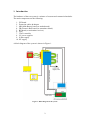
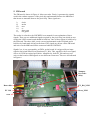
Pixel HPD Test System Hardware Description
Version 1.0
K. Wyllie, June 2004
Table of contents
1.
2.
3.
4.
5.
6.
7.
Introduction............................................................................................................2
ZIF board ...............................................................................................................3
Extension cables & adaptor ...................................................................................5
MB board ...............................................................................................................6
FB board.................................................................................................................9
FLIC and RX card................................................................................................11
JTAG controller and configuration......................................................................12
1
1. Introduction
The hardware of the test system is a mixture of custom and commercial modules.
The main components are the following:
1. ZIF board
2. Extension cables & adaptor
3. MB (Mike Burns) board (or motherboard)
4. FB (Francois Bal) board (or transmitter board)
5. RX board (or mezzanine receiver)
6. FLIC
7. JTAG controller
8. LV power supplies
9. Si bias supply
10. HV supply
A block diagram of the system is shown in Figure 1.
Figure 1: Block diagram of the system
2
2. ZIF board
This is a mostly passive board on which a Zero-Insertion-Force (ZIF) socket is
mounted. It is shown in Figure 2. This socket can hold a complete HPD or a ceramic
carrier before it is encapsulated within an HPD. The ZIF sockets used in the test
systems are special test sockets, designed for robust insertion and removal of the
device. But please note that they allow the device to be inserted the wrong way round.
Please check that the orientation is correct when inserting an HPD or carrier, as
indicated in Figure 3.
The ZIF board receives/transmits signals via the two black connectors J1 and J3. The
signals are described in detail in the LHCBPIX1 chip user manual. Termination of the
data output signals is done by four resistor packs mounted on sockets. These can be
removed if necessary (eg if the extension cable is used - see below).
There are access points to allow monitoring of test pixels within the HPD. Details of
these are in the LHCBPIX1 chip user manual.
Supply voltages can be monitored on the board on the pins of connector J5.
J1
J3
J5
Figure 2: The ZIF board with a carrier mounted
3
Keyed corner of
carrier is here,
matched with white
marker on ZIF
sockets
Figure 3: Zoom of the ZIF board showing the orientation of the carrier in the socket
4
3. Extension cables & adaptor
The extension cables allow mechanical freedom of the ZIF board with respect to the
rest of the system. The cables consist of two double-layer twisted pair cables which
plug into connectors J1 and J3 of the ZIF board. The other ends of the cables plug into
a small adaptor board which in turn plugs into the MB board. On this adaptor board
are four resistor packs, connected to terminate the data output bus from the HPD. If
the extension cables and adaptor board are used, the termination resistor packs on the
ZIF board should be removed.
5
4. MB board
The MB board plays two major roles in the system:
a) It generates all the power supplies and reference signals needed by the pixel
chip, and transmits them to the ZIF board. These power supplies are all
adjustable via software (with the exception of Vtt_digital and Vtt_analog,
which are adjusted by potentiometers). The power supply voltages and their
currents can also be monitored via software using ADCs on the board.
b) The MB board translates the levels of the pixel chips signals into those
required by the external electronics and vice versa. The pixel chip uses GTL
signals. Its output signals are translated by the MB board into TTL and then
into LVDS in which form they are transmitted off the MB board. Signals
arriving to the MB board are LVDS, and are translated to TTL and then to
GTL.
The MB board is configurable by JTAG through cable JTAG_MB shown in Figure 4.
Switching on/off the power to the ZIF board, setting the voltages and monitoring are
all done by JTAG. The JTAG signals to the HPD also pass through the MB board (on
cable JTAG_chip) but are only translated to GTL and nothing more.
There are red LEDs on the board used as status indicators. These are indicated in
Figure 4. LED1 will flash when there is JTAG communication with the board. LED2
will be on or off depending on whether power is supplied to the pixel chip or not.
The power supplies and reference voltages generated by the MB board for the pixel
chip are the following:
1) Vdd_Digital
: digital power supply
2) Spare_Digital
: spare supply referenced to digital ground
3) Well_Digital
: n-well connection for digital circuitry
4) GTL_Ref_Digital : reference voltage for GTL signaling
5) Vdd_Analogue
: analogue power supply
6) Spare_Analogue : spare supply referenced to analogue ground
7) Well_Analogue
: n-well connection for analogue circuitry
8) GTL_Ref_Analogue: reference voltage for GTL signaling of JTAG
9) DAC_REF_MID : reference for internal pixel DACs
10) DAC_REF_VDD : reference for internal pixel DACs
11) Test_DAC_Lo : reference level for calibration pulse
12) Test_DAC_Hi
: reference level for calibration pulse
13) Test Pulse Fine Delay: fine delay (0.5ns unit steps) for calibration pulse
The user is referred to the pixel chip user manual for more information on these
voltages.
Signals between the MB board and the FB board are on two twisted pair cables which
arrive on connectors DATA and CONTROL. The DATA connector transmits the 32
bits of data from the HPD, and the CONTROL connector receives control signals
6
(clock, strobe etc) from the FB board which are then re-transmitted to the HPD. The
user should ensure that these connectors are plugged in properly.
LED 1
DATA
CONTROL
LED2
Sensitive
Transistor
JTAG_MB
JTAG_chip
Figure 4: The MB board
The MB board requires three power supplies, as indicated in Figure 5:
i) +5V analog
ii) -5V analog
iii) +5V digital
There are connections for the analog and digital grounds, although these should be
connected together at the board.
The MB board does no formatting of the data.
MB board known problems:
1) After powering on, the board can sometimes be in an unusable state. An
indication of this is the incorrect reading of the power supply currents or
voltages (eg the current readings are sometimes 39A, which is an indication
that the board is operating incorrectly). This can be cured by a simple power
off and on of the 5V supplies.
2) After intensive use of the board, one component has failed a few times. This is
a power transistor used to buffer the digital 1.8V power supply to the pixel
chip, and is indicated in Figure 4. If this component fails, the 1.8V digital
supply will not be provided to the chip, and the transistor itself may be
discoloured. It can easily be replaced.
7
+5V analog
+5V dig
GND
-5V analog
GND
GND +5Vd unused +5Va GND
-5Va
Figure 5: Zoom of MB board and schematic showing the power supply connections
8
5. FB board
The FB board is shown in Figure 6. It has two tasks. Firstly, it generates the signals
used in the readout sequence of the pixel chip and transmits them to the MB board
that in turn re-transmits them to the pixel chip. These signals are:
i)
ii)
iii)
iv)
v)
vi)
clock
strobe
nevr
ce
data_reset
test_pulse
The reader is referred to the LHCBPIX1 user manual for an explanation of these
signals. There are two additional signals required by the pixel chip, but which are not
used in the LHCb scenario and should be held low. One of these (abort) is held low by
the FB board. The other (shift_reset) was not implemented on the FB board and is
held low by hand-made wiring on the board. The signals are driven off the FB board
and arrive on the MB board on the connector labeled CONTROL.
Signals i) to vi) are generated by an FPGA on the board. It is triggered by an input
signal to the board called Event_Readout (EV_RO). This, together with a reset signal,
arrives in LVDS on twisted pair cables. Alternatively, both EV_RO and reset can
arrive at the board as NIM signals on two different connectors. These are all indicated
in Figure 6.
Jumpers
for strobe
delay
Data cable
EV_RO_NIM
EV RO
Reset_NIM
reset
Figure 6: The FB board
9
The second task of the FB board is to receive the data from the MB board and
transmit it down a serial link. Data from the MB board is buffered, formatted and then
serialized onto two twisted pairs at a rate of 40MHz. These pairs are contained within
a network cable which plugs into a RJ45 connector on the board. The formatting of
the data is done according to the S-link protocol chosen for the data transmission.
This is transparent to the user.
There are a number of LED indicators on the FB board, and the user should check
these to verify the correct set-up of the board. The user can also select different modes
of operation. ALICE or LHCb mode can be selected with a switch. SINGLE or
MULTI mode can also be selected. SINGLE mode is the standard mode of operation,
and means that a single trigger and readout sequence is initiated by EV_RO. MULTI
mode means that a burst of triggers and readout sequences will be generated by the
arrival of EV_RO. The test_pulse can be disabled/enable by means of a jumper. The
board can be put into a link-test mode, where it generates a fixed pattern and transmits
this down the link. This is again done by a jumper.
Finally, the time between the test_pulse and the strobe can be changed in steps of
25ns by means of a series of jumpers. The positions of these jumpers are indicated in
Figure 6. The delay setting on the FB board when it is delivered corresponds to a
setting of 7 in the delay_control register of the pixel chip.
The FB board also contains a number of general purpose level adaptors. The user is
referred to the board schematic for the location of these devices.
10
6. FLIC and RX card
Data transmitted from the FB board is received by the RX card mounted as a
mezzanine on the FLIC PCI card in a PC. The RX card is designed to de-serialize the
data and transmit it still in S-link format to the FLIC. The FLIC writes this data to
memory which can be accessed through PCI. The FLIC is programmed to generate
the EV_RO and reset signals when requested by software.
The cabling of the RX card and FLIC are shown in Figure 7.
FLIC known problems:
1) The FLIC has shown some sensitivity to temperature. It is recommended that
it is installed in a PCI slot far from other cards. In some cases it has been
necessary to use a fan if the adjacent PCI slots are full and take the cover off
the PC.
2) When installed and powered correctly, the green LEDs on the FLIC should
flash on and off. If they show no sign of activity, the PC should be powered
off and re-started. (In some cases, this has required a change of PCI slot).
3) Occasionally, when operating the system a software error message will appear
saying “Error – event buffer empty”. A possible cause of this error is that the
data cable from FB board to RX card is not plugged in properly. If the
problem persists, the user should shut down the LABVIEW software and restart. The ultimate solution is to re-boot the PC.
4) If any other error messages appear, the user should try re-starting the software
or the PC.
EV_RO
Reset
Data cable
Figure 7: FLIC and RX_card with cables
11
7. JTAG controller and configuration
The MB board and pixel chip are configured using the JTAG protocol.
Any commercial JTAG controller can be used as long as it provides TTL signals and
can drive two channels, one for MB and one for the pixel chip.
The FB is not configurable via software. The FLIC is configurable via PCI.
12