1
NEAT-286 USER'S MANUAL SEAT System Board
CHAPTER ONE THE SYSTEM INFORMATION 1.1 SPECIFICATION • 16MHz 80286 for 16120MHz system operation with 0.5-0.7 wait
states for lOOns DRAM
• Hardware and software compatibility with IBM PC/AT New
Enhanced AT (SOLUTION) CHIPSet for 12MHz to 16MHz
• Page interleaved memory supports single bank page mode, 2 way
and 4 way page interleaved mode
• Integrates Lotus-Intel-Microsoft Expended Memory Specification
(LIM EMS) memory controller on board. to supports EMS 4.0 or later
• Supports 2 MByte up to 8 MByte
• Support two kind of RAM CARD, 640KB and 2MB version
• Socket for 80287 Math coporcessor
• 12, 12/16, 16120 MHz three version motherboard
• System clock switchable with H/W, S/W and Keyboard
• Light indication for system turbo speed
• Real time clock/calendar with CMOS RAM and backup battery
2
SEAT System Board
1 . 2 SYSTEM OVERVIEW The system is designed for using in 12 to 16 MHZ 80286 based
systems included the CS8221 SOLUTION CHIPset (n1) and provides
complete support for the IBM PC/AT bus.
The CS8221 SOLUTION CHIPSet (no consists of tht> X2C211
CPU/Bus controller, the 82C212 Page/Interleave and EMS
M,emory controller, the 82C215 Data/Address buffer and the
82C206 Integrated Peripherals Controller (IPC).
The SOLUTION CHIPSet(TM) supports the local CPU bus, a 16 bit
system memory bus and the AT buses as shown in the SOLUTION
System Block Diagram. The 82C211 provides synchronization and
control signals for all buses. The 82C211 also provides an
independent AT bus clock and allows for dynamic selection _,
between the processor clock and the user selectable AT bus clock.
Command delays and wait states are software configurable,
providing flexibility for slow or fast peripheral boards.
3
,
,
'
.
SEAT System Board
The 82C212 Page/Interleave and EMS Memory controller
provides an interleaved memory sub-system design with page
mode operation. It supports up to 8 MB of on-board DRAM
with combinations of 64Kbit, 256Kbit and IMbit DRAMs. The
processor can operate at 16MHz with 0.5-0.7 wait state memory
accesses, using 100 ns DRAMs. This is possible through the
Page Interleaved memory scheme. The Shadow RAM feature
allows faster execution of code stored in EPROM. By down
loading code from EPROM to RAM. The RAM then shadows
the EPROM for futher code execution. In a DOS env1f(:lnment..
memory above 1Mb can be treated as LIM EMS memory.
The 82C215 Data/Address buffer provldes the buffering and
latching between the local CPU addl ess bus and the Peripheral
address bus. It also provides buffenng between the local CPU
data bus and the memory data bus. The parity bit generation and
error detection logic resides in the 82C2I5.
4
SEAT System Board
82C211 BUS CONTROLLER
The 82C211 Bus Controller consists of the following functional
sub-modules.
- Reset
~nd
Shut Down Logic
When the system cold started, the 82C211 asserts a reset
signal for a system reset to reset the
AT Bus, 82C206 IPC,8042
Keyboard controller, the 82C212 memory controller, and
all of the system. The other reset signal is generated from
the 8042(8742) Keyboard controller when a "warm reset" is
required. The warm reset activates a -reset signal the reset
the 80286 CPU only.
- Clock Generation and Selection
The 82C211 provides a flexible clock selection. It has two
inputs clocks; CLK2IN and ATCLK.Typically the ATCLK
Should be of a lower frequency than CLK2IN. ATCLK
and CLK2IN can be selected under program control.
5
I
"
SEAT System Board
The 1'12C211 generates prol'e!:>sor clock PROCCLK for
driving the CPU state machine and interface. SeLKC
(internal), is PROCCLK/2 and is in phase with the
internal states of the 80286. BCLK (internal) is the AT Bus
state machine clock and is used for the AT bus interface.
SYSCLK is the AT bus system clock and is always
BCLK/2.
PROCCLK can be drived from CLK2lN or from ATCLK.
In the synchronous mode, both PROCCLK and BCLK arc
drived from CLK2IN. so that the processor state m:lchine
and the AT bus state machine run synchronous. In the
asynchronous mode, BCLK is generated from the ATCLI\.
and PROCCLK is generated from CLK2IN or the
ATCLK. In this case, the processor and AT bus state
machines run asynchrounous to each other.
The following clocks selections are possible:
6
SEAT S,ystem Board
Synchronous mode:
1 PROCCLK = BCLK
SYSCLK = BCLK/2
= CLK2IN
= CLK2IN/2
2 PROCCLK = CLK2IN
BCLK = CLK2IN/2
SYSCLK = BCLK/2 = CLK2IN/4
3 PROCCLK = BCLK
SYSCLK = BCLK/2
= CLK2Il'i/2
= CLK2IN/4
Asynchronous mode:
1 PROCCLK = CLK2IN
BCLK = ATCLK
SYSCLK = BCLK/2 = ATCLKj2
2 PROCCLK = ATCLK
BCLK = ATCLK
SYSCLK = BCLK/2 = ATCLK/2 .
Under normal operation, CLK2IN should be selected as
the processor clock (PROCCLK) to allow-the processor to
run at full speed.
7
I
SEAT System Board
- CPU State Machine, Bus State Machine,
8us arbitration. and Refresh Logic
In order to extract maximum performance out of the 80286
on the system board, it is desirable to run the system board
at the rated maximum CPU frequency. The frequency may
be too fast for the slow AT BUS. In order to overcome
this problem, the 82C211 has two state machine: the cpe
state machine which typically runs off CLK2IN, and the
AT bus state machine which runs off BCLK. The 82C211
also controls all bus activity and provides arbitration
between the CPU. DMA/Master devices and DRAM
refresh logic.
8
SEAT System Board
- Port Band NMI Generation Logic
The 82C211 provides assess to Port B defined for the
PC / AT as shown in th is Figure:
10 ADDR
61H
7
6
0
5
4
3
2
1
PCK CHK T20 RFD E1e EPR SPK T2G
PORT B
Read/
Write
Function
Bits
7
6
5
4
R
R
R
R
PCK-System memory parity check
CHK-1/O channel check
T2Q-Timer 2 Out
RFO-Refresh Detect
EIC-Enable I/O channel check
ERP-Enable system memory
parity check
SPK-Speaker Data
T2G-Timer 2 Gate (Speaker)
3
2
1
o
R/W
R/W
R/W
R/W
Port B register definition
9
SEAT System Board
The NMI sub-module perf()fms the latching and enabling of I/O
and parity error conditions, which will generate a non-maskahle
interrupt to the CPU if NMI is enabled. Reading Port B will
indicate the source of the error condition (lOCK AND PCHK).
Enabling and disabling of NMI is accomplished by writing to I/O
address 070H. On the rising edge of XIOW. NMI will be
enabled if data bit 7 (XD7) is equal to 0 and will be disabled if
XD7 is equal to 1.
10 s EAT System Board
- Numeric Co-processor Interface
Incorporated in the R2C211 is the circuitary to interface an
80287 Numeric Co-processor to R0286. The circuitary
handles the decoding required for selecting and resetting
the Numeric Co-processor, handling -NPBUSY and
ERROR signals from the S0287 to the CPU, and
generating interrupt signals for error handling.
The -NPCS signal is active for I/O address OFSH-OFFH,
used to access the internal registers of the 80287. It is also
active for I/O addresses 070H-NMI mask refister. OFOH~
Clear the Numerical Co-processor and Numerical Co
processor BUSY signal. While executing a task, the 80287
issues an-NPBLJSY signal to the 82('211. Under
normal operation, it is passed out to the CPU as -BUSY.
If during this husy period, a numeric co-processor error
occurs. -ERROR input to the R2C211 becomes active,
resulting in latching of the BUSY output and assertion of
NPINT. Both signals stay active until cleared by an I/O
write cycle to address OFOH or OFIH. A system reset
clears both NPINT and -BUSY latches in the 82C211. The
80287 is reset through the NPRESET output, which can be
activated by a,system reset or.by performing a write
operation to I/O port OF1H.
11 SEAT System Board
• Modes of Operation of the 82C211
The 82C211 has 4 modes of operation for different CPU
and Al bus clock selections:
Normal mode Quick mode Delayed mode External mode * Normal Mode
This mode is enabled by default (without writing to
the registers of 82C211).
Under Normal mode:
PROCCLK = CLK2IN
BCLK = CLK2IN /2
SYSCLK = CLK2IN /4
If activated by default, I/O cycles will have one
command delay,S bit AT memory cycles will have 4
wait states, 16 bit AT memory cycles will have 1
wait state.
12 SEAT System Board
* Quick Mode
This mode is also a synchronous mode and is
enabled by writing a zero to REG61 < 6 > and the
following clock selections have been made:
PROCCLK = BCLK = CLK2IN
SYSCLK = CLK2IN/2
Quick mode is performance efficient when
switching between local and AT bus cycles. This
mode i!; useful for high speed add-on cards such as
Laser Printer interface cards.
* Delayed Mode
This mode is another synchronous mode and is
enabled when Quick mode is disabled and the
following clock selections have been chosen made:
PROCCLK = CLK2IN
BCLK = CLK2IN
SYSCLK = CLK2IN/2
This mode is useful for slow peripheral AT add-on
cards.
13
SEAT System Board
* External Mode
This is an asynchronous mode and is enabled when
ATCLK is selected as the source for BCLK. The
following clock selections are required in this mode:
PROCCLK = CLK2IN
BCLK = ATCLK
S YSCLK = ATCLK/2
chronized with CLK2IN. The CPU samples
READY low in sequence 10 and terminates the
current cycle.
- Configuration Registers
,here are three bytes of configuration registers in the
82C211; RAO, RAl and RA2. An indexing scheme is used
to reduce the I/O ports required to access all the registers
required for the SOLUTION CHIPSet. Port 22H is used as an
indexing register and Port 23H is used as the data register.
The index value is placed in port 22H to access a particular
register and the data to be read from or written to that
register is located in port 23H. Every access to port 23H
must be preceded by a write of the index value to port
22H even if the same register data is being accessed again.
14
SEAT System Board
All reserved bits are set to zero by default and when
written to, must be set to zero. Table 1 lists the three
registers:
Table 1.
RAO, RAI, and RA2
Register
Number
Register
Name
RAO
RAI
PROCCLK Selector
Command Delay
Wait State/
BCLK Selector
R1>.2
15 Index
60H
6IH
62H
SEAT System Board
82C212 PAGE/INTERLEAVE AND EMS MEMORY CONTROL[
The 82C211 performs the memory control function in the systen:
The 82C211 organizes memory as banks of 18 bit modules
consisting of 16 bits of data and 2 bits of parity, informaiton. Th
16 bits of date are split into high and lower bytes with 0 parity bi:
for each byte. The minimum configuration can be a single bank
operating in non-interleaved mode or can he a pair of DRAM
banks operating in two way interleaved mode, the DRAMs withi:
a pair of banks must be indentical.
However, each bank of DRAM pairs can he different from other
pairs. For example, Banks 0,1 may have 256K by 1 bit DRAM
and Banks 2.3 could have 1M by 1 bit DRAMs. A typical system
may be shipped with one or two banks of smaller DRAM types
(e.g. 256 by 1 bit DRAMs) and later upgraded with additional
pa.jrs of banks of larger DRAMs (eg. 1M by 1 bit DRAMs)
22 SEAT System Board
II
Page/Interleaved Operation
I
The 82C212 uses a page/interleaved design that is different from
most interleaved memory designs. Typical two way interleaving
schemes use two bar:ks of DRAMs with even word addressses on
one bank and odd word addresses on the other bank. If memory
acesses are sequential, the RAS precharge time of one bank
overlaps the access time of the other bank. Typically, program'
consist of insturction fetches interspersed with operand acces~e" ..
The instruction fetches tend to be sequential and the oreranJ
accesses tend to be random.
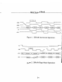
Figure 1 is a sequence diagram for a memory interleaved scheme
using two banks 0 and 1. The -RAS signals of the. two banks are
interleaved so that the RAS precharge time (Trp) of one bank i~
used for the -RAS active time in the other bank. This requires
sequemial acesses to be alternationg between the two hanks. For
non-sequential accesses it is possible to get wait states due to a
'miss'. Typically this results in a 50S'r hit ratio (possible zero wait
state accesse'i)
23 SEAT System Board
DATA
_ _ _~
Figure 1. DRAM Interleaved Operation
~ --'~-------------
_______________~r---
i
I
i
"OOR
OAT.. ---~
Figure 2. DRAM Page Mode Operation
24 SEAT System Board
Figure 2 is a sequence diagram of a paged
mode DRAM operation. In paged mode DRAMs. once a row
access has been made, it is possible to access subsequent column
address within that row, without the -RAS precharge penalty.
However, after a -RAS active timeout, there is a -RAS precharge
period which typically occurs every 10 microseconds. Since the
CAS precharge time Tcp is small, it is possible to make fast
random accesses within a selected row. Typically, page mode
access times are half the normal DRAM access times. For 256K x
1 DRA:v1s, each row has 512 bits. If eighteen 256K x 1 bit
DRAMs are used to implement a hank, a page would have 512 x 2
bites (excluding 2 bits for parity) = 1 Kbytes. Thus paged mode
DRAMS could he interleaved at 1 Kbyte boundaries rather than 2
byte boundaries as in the regular interleaved mode operation.
Any access to the currently active -RAS page would occur in a
short page access time and any subsequent access could he
anywhere in the same 1 Kbyte boundary, without incurring any
penalty due to -RAS precharge. If memory is configured to take
advantage of this DRAM orgaization, significantly better
performance can be achieved over normal interleaving because:
1. Page mode access time is shorter than normal DRAM
access time, This allows more time in the DRAM critical
paths, to achieve penalty free accesses or 'hits',
25 SEAT System Board
2. The possiblity of the nxt access being fast is significantly higher
than in a reguiar interleaving scheme. This is because
instructions and data tend to cluster together by principle of
locality of reference.
RASa
~~
____________________________________~
DATA - - - - ' - - {
Figure 3. DRAM Page/Interleave Operation
Figure 3 is a sequence diagram of a two way Page/Interleaved
scheme using page mode DRAMs. As seen, it is possible to make
zero wait stae accesses between the two banks 0 and 1, by
overlapping -CAS precharge time of once bank with -CAS active
time of the other baI1k. The DRAM -RAS lines for both banks
can be held active till the -RAS active timeout period, at which
time a -RAS precharge for that bank is required. Typical hit
ratios higher than 80% are possible using this scheme. With the
82C212 memory controller, using the page/interleaved scheme,
150 nanosecond access time DRAMs can be used at 12MHz and
100 nanosecond access time DRAMs at 16MHz.
26
SEAT System Board
OS/20PTIMIZATIO:,,/
The SOLUTION architecture feature OS/2 optimization using
REG67 < 1 > of the 82C212 in conunction with REG60 < 5 > 0 f
the 82C211. OS/2 makes frequent DOS calls while operating in
protected mode of the 80286 CPU. In order to service these
DOS calls, the 80286 CPU has to switch from protected to real
mode quickely. Typical PC/AT architectures require the prcessor
to issue two commands to the 8042 (or 8742) keyboard
controller in order to reset the pocessor (to switch it into
protected mode) and to activate GATEA20.
REG60< 5 > of the 82C211 is to used to invoke a software reset
to the 80286 processor and REG67 < 1 > is used to activate
GATEA20. Sincer this involves the I/O writes, it is possible to
execute a "Fast GATE20". In an OS/2 environment, where
frequent DOS calls are made, this feature provides signficant
performance improvement.
27 CHAPTEP THREE CONNECTORS AND JUMPER SETTING CONNECTORS:
13 - EXTERNAL BATTERY CONNECTOR
PIN
FUNCTION
1
GND
SHORT WITH PIN 3 FOR INTERNAL BATTERY
2
3
4
EXTERNAL BATTERY POWER
J4 - SPEAKER CONNECTOR
PIN
FUNCTION
1
2
SPEAKER SIGNAL
N.C.
GND
+5V
3
4
J5 - KEYLOCK CONNECTOR
PIN
FUNCTION
1
2
POWER LED
KEY
GND
KEYLOCK
GND
3
4
5
92
J6 - KEYBOARD CONNECTOR
PIN
FUNCTION
1
2
3
4
5
KEYBOARD CLOCK
KEYBOARD DATA
N.C.
GND
+5V
PSlIPS2 - SWITCHING POWER SUPPLY CONNECTOR
PIN
FUNCTION
2
3
4
5
6
POWER GOOD
+5V
+ 12V
-12V
GND
GND
1
2
3
4
5
6
GND
GND
-5V
+5V
+5V
+5V
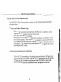
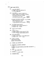
93 NEAT·SMT JUMP SETIING
JP! - ROM SIZE SELECT
2,3 SHORT 256K ROM (DEFAULT)
1,2 SHORT 128K ROM
JP2 - RAM INSTALL SELECT (DEF AUL T)
I: SELECT SIMP AS LO BANK (0,1 BANK), DIP-RAM HI BANK (2,3 BANK) 1-2,3-4,6-7,8-9,11-12,13-14
SHORT 16-17,18-19,21-22,23-24,26-27,28-29 SHORT 2: SELECT DIP-RAM AS LO-BANK (0,1 BANK), SIMP HI-BANK (2,3 BANK) 2-3,4-5,7-8,9-10,12-13,14-15
SHORT 17-18,19-20,22-23,24-25,27-28,29-30 SHORT JP3 - 287 MODE (SYNC/ ASYNC)
2,3 SHORT ASYNC MODE (DEFAULT)
1,2 SHORT SYNC MODE
JP4 - RESET (HARD WARE)
JP5 - TURBU WITCH
[,2 SHORT TURBO MODE (SELECT OSC2l
1,2 OPEN NORMAL MODE (SELECT OSCI)
JP6 - 287 CLOCK MODE
2.3 SHORT FOR ASYNC CLOCK (DEFAULT) [,2 SHORT FOR SYNC CLOCK JP7 - DISPLAY MODE
OPEN MONO MODE
SHORT COLOR MODE
LEI - TURBO LED CONNECTOR
13 • EXTERNAL BATTERY CONNECT
1 +5V
2,3 SHORT ENABLE INTERNAL BATTERY CHARGE COME
4 GND
J4 - SPEAKER CONNECTOR
J5 - POWER LED & KEY LOCK
J6 - CONNECT HEAD
94
eft
~
c
.,c'"
~
~
!:l
r
~
!:l
~
2
0
(")
'"<:>
'" '" ...
:e c
~ ~
:e>
<:>
~
§
;l!
'"
~
:;;
);;
In
It 311
CtO
CH
U103
U1RJO
1'"
C49
Ut17
t1
~Ul26
Ul2i'
U10"
Ul
Il~
em
C/8
n
CB3,
68
51
12 C50
U1
1JJ.94
SILK SCREEN
~ ~
Jf'3
LeO""
~
r
'81
181
Desl
181
lei
Q
£2f
C103
C113[]
7<R3
287 Moor (SYNC ASYNC)
UI'" I
"O'"'
7S
inO
1l,J
JOSut41 CJ
,;13
J04
JC3
J03
:
(po
..
+r:y:o
"'"
I
3
.02 0
C53 .. C!I5
+000+
D4t
'eo<
131
G40 .. C42
C29
9(0
.0 Q, 0+
C18 •
+0 ~ u·
[
On
+
t
~
[[Ife----'[
COlI Ul64
JP7 - DISPLAY MODE
[If
~
:::::C32
ute::::::
=df9
H
11
Ii
U
It
'-At
::
~
q
I3!EJY3
lJ:::j
f=k
8T!
O'~ Oqo;gQ;,Q2~ ~
J"'
u'~1
m
I~I ~
Ii
D0
~:: R1.0n+O.~I[1 ~
,.5
JFt"
'51
JQ3
-C1
-.ao Cfo.
!1
!l
R05102
[I)r'5+5-5GG G-12 .l2<S}'1
1
~::
FU
a;
Hie,
~B" .c:J- .. ~
~.[ 1
Rl" R15
.
JP6 - CLOCK MODE
' ...,9"
11 311
R18
1'3,1
11 311
'(P!
11]11
il 3tI
:~
ID?
~:;
1Ii lOr
~fr~[]~r~~lc=::J ,--------.,~
UIB2
[IL~[t~d'2~
gl~71 ~~~C111
f'()ct7
311
~~
,
Jel
_'1
JAI
+Ors
JUt
311
3tC::=
-~:::J
+0""'" ,....., L
~I
~
~
[ut02
IUE
lwe:.
.~"
'm
•
~I!
IN3tl
"1
[I f
{h
C3
181
R2LP3'.1I3
19
=l
0'1
W
ROM SIZE SELECT
~~ [13~<IS~CJ-Rl0JC<RIlBI'3~C70-c:::J-.
.
•
r
ut"~r~1i~n~~I::~~
UlBl
~"
~[I~[I
UI69
~[I~[I~[I~[I~
Ul~~[I~[j~[j'~[j
Ul$
~~ci'J~ ~l~~cIJ
32
;CU'5
Ul22
"'~~U~U~[[J ~
U1F===l U1«3
COl
Cll2
~[I£E:l§3[I~[I~[1
UHl
""
11
[Ill-;:==;;=::;1
l.RQ
JPI
....... 1\..)
CI5[)~1- - - = ; I
C<
------,[~fl~\i~[1
"n2~ ~I"" I
!""
~~
f"
J£l
JO
~[I~[j~IT~rril
~33
~3-4
ilh"J5
1
I
I
I[
t!d
b
0
(
(
~6.
30
~[IC2
U100
IJQ'" 3t!
:23a~.;::::nrn:::::::~3
,I
,I
.OC9
+0 el3
I
I
181
181
JP2· RAM INSTALL SElECT
X
~
~
'"
'"--<
;;;
~
<:>
:z:
~
!:l
o
z
~
(")
<:>
'"
~
.,"'"<
a;