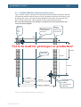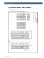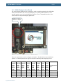
1
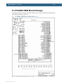
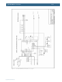
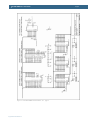
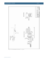
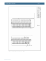
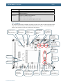
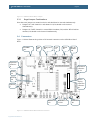
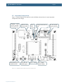
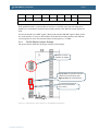
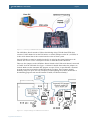
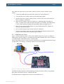
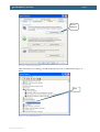
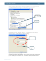
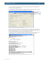
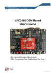
LPC2468 OEM Board - User’s Guide
Copyright 2007 © Embedded Artists AB
LPC2468 OEM Board
User’s Guide
Get Up-and-Running Quickly and
Start Developing Your Applications On Day 1!
EA2-USG-0702 v1.0 Rev B
LPC2468 OEM Board - User’s Guide
Page 2
Embedded Artists AB
Ole Römers väg 12
SE-223 70 Lund
Sweden
[email protected]
http://www.EmbeddedArtists.com
Copyright 2005-2007 © Embedded Artists AB. All rights reserved.
No part of this publication may be reproduced, transmitted, transcribed, stored in a retrieval
system, or translated into any language or computer language, in any form or by any means,
electronic, mechanical, magnetic, optical, chemical, manual or otherwise, without the prior
written permission of Embedded Artists AB.
Disclaimer
Embedded Artists AB makes no representation or warranties with respect to the contents
hereof and specifically disclaim any implied warranties or merchantability or fitness for any
particular purpose. Information in this publication is subject to change without notice and
does not represent a commitment on the part of Embedded Artists AB.
Feedback
We appreciate any feedback you may have for improvements on this document. Please send
your comments to [email protected].
Trademarks
InfraBed and ESIC are trademarks of Embedded Artists AB. All other brand and product
names mentioned herein are trademarks, services marks, registered trademarks, or registered
service marks of their respective owners and should be treated as such.
Copyright 2007 © Embedded Artists AB
LPC2468 OEM Board - User’s Guide
Page 3
Table of Contents
1 Introduction
4
1.1
Features
4
1.2
ESD Precaution
5
1.3
Other Products from Embedded Artists
5
1.3.1
Design and Production Services
5
1.3.2
LPC2xxx OEM / Education / QuickStart Boards and Kits
6
2 LPC2468 OEM Board Design
2.1
LPC2468 OEM Board Schematics, v1.1
7
2.1.1
CPU
2.1.2
Powering
12
2.1.3
Analog Inputs/Outputs
12
2.1.4
Ethernet Interface
12
2.1.5
External Memories
13
2.1.6
External Memory Interface
13
2.1.7
USB-OTG
14
2.1.8
Reset Generation
14
2.1.9
I2C E2PROM
14
2.1.10
Expansion Connectors
12
14
2.2
Memory Layout
14
2.3
Usage of CPU Pins
15
2.4
LPC2468 OEM Board Mechanical Dimensions
17
3 OEM Base Board Basic Design
18
3.1
OEM Base Board Basic Schematics, v1.1
18
3.2
Usage of CPU Pins
23
3.3
Jumpers
3.3.1
Illegal Jumper Combinations
27
28
3.4
Connectors
28
3.5
Important Components
29
3.6
QVGA Display Add-on Board
30
3.6.1
QVGA Display Jumper Settings
4 Getting Started
31
32
4.1
Basic Requirements
32
4.2
Initial Setup and Powering
32
4.3
LAN/Ethernet Setup
34
4.4
FTDI USB Driver
35
4.4.1
USB Driver Behavior
5 CD-ROM and Product Registration
5.1
Product Registration
6 Further Information
Copyright 2007 © Embedded Artists AB
7
39
40
40
41
LPC2468 OEM Board - User’s Guide
Page 4
1 Introduction
Thank you for buying Embedded Artists’ LPC2468 OEM Board based on NXP’s
ARM7TDMI-S LPC2468 microcontroller.
This document is a User’s Guide that describes the LPC2468 OEM Board and the OEM Base
Board Basic hardware design. There is a separate document describing program
development for the LPC2xxx series in general.
1.1 Features
Embedded Artists LPC2468 OEM Board with NXP’s ARM7TDMI LPC2468
microcontroller lets you get up-and-running quickly. The small form factor OEM board
offers many unique features that ease your learning curve and program development. The
board has also been designed for OEM applications with volume discount available.
•
NXP's ARM7TDMI LPC2468 microcontroller in BGA package, with 512 KByte
program FLASH and 96 KByte SRAM
•
External FLASH memories: 128 MB NAND FLASH and 4 MB NOR FLASH
•
External data memory: 32 MB SDRAM
•
12.0000 MHz crystal for maximum execution speed and standard serial bit rates,
including CAN and USB requirements
•
32.768kHz RTC crystal with 0.3F capacitor backup power
•
100/10M Ethernet PHY/interface based on Micrel KSZ8001L
•
USB-OTG support on USB-A channel via external ISP1301 chip
•
256 Kbit I2C E2PROM for storing non-volatile parameters
•
Buffered 16-bit databus for external expansion
•
Connector: 2x96 pos connector (2 x 3 rows with 32 pos), 2mm pitch
−
All LPC2468 pins available (except a few used for Ethernet and USB-OTG
interface)
•
+3.3V only powering
•
Onboard reset generation
•
Compact dimension: 66 x 70 mm
−
Six layer PCB design for best noise immunity
There is an accompanying OEM Base Board, version Basic that can be used for initial
prototyping work. The features of the board are:
•
•
Copyright 2007 © Embedded Artists AB
Connectors
−
192 pos, 2mm pitch connector for LPC2468 OEM Board
−
Ethernet connector (RJ45)
−
MMC/SD interface & connector
−
JTAG connector
−
Pads for ETM connector
Interfaces
LPC2468 OEM Board - User’s Guide
•
−
USB OTG interface & connector
−
USB device interface & connector
−
USB host interface & connector
−
Full modem RS232 on UART #1
−
CAN interface & connector
Power
−
•
•
Page 5
Power supply, either via USB or external 9-15V DC
Expansion
−
Color QVGA LCD expansion connector (serial and parallel interface options)
−
WLAN module (IEEE802.11b) expansion connector
Other
−
5 push-button keys (four via I2C and one on P2.10)
−
5 LEDs (four via I2C and one on P2.10)
−
2 Analog inputs
−
USB-to-serial bridge on UART #0 (FT232R) and ISP functionality
−
Reset push-button and LED
−
All OEM Board signals available on expansion connector/pads
−
240x150 mm in size
1.2 ESD Precaution
Please note that the LPC2468 OEM Board and OEM Base Board Basic come without any
case/box and all components are exposed for finger touches – and therefore extra attention
must be paid to ESD (Electro-Static Discharge) precaution.
Make it a habit to always first touch the metal surface of one of the USB connector for a
few seconds with both hands before touching any other parts of the boards. That way, you
will have the same potential as the board and therefore minimize the risk for ESD.
Never touch directly on the LPC2468 OEM Board and in general as little as possible on the
OEM Base Board Basic. The keys on the OEM Base Board have grounded shields to
minimize the effect of ESD.
Note that Embedded Artists does not replace boards that have been damaged by ESD.
1.3 Other Products from Embedded Artists
Embedded Artists have a broad range of LPC2xxx (and soon LPC3xxx) based boards that
are very low cost and developed for prototyping / development as well as for OEM
applications. Modifications for OEM applications can be done easily, even for modest
production volumes. Contact Embedded Artists for further information about design and
production services.
1.3.1
Design and Production Services
Embedded Artists provide design services for custom designs, either completely new or
modification to existing boards. Specific peripherals and I/O can be added easily to different
designs, for example, communication interfaces, specific analog or digital I/O, and power
supplies. Embedded Artists has a broad, and long, experience in designing industrial
Copyright 2007 © Embedded Artists AB
LPC2468 OEM Board - User’s Guide
Page 6
electronics, in general, and with NXP’s LPC2xxx microcontroller family, in specific. Our
competence also includes wireless and wired communication for embedded systems. For
example IEEE802.11b/g (WLAN), Bluetooth™, ZigBee™, ISM RF, Ethernet, CAN, RS485,
and Fieldbuses.
1.3.2
LPC2xxx OEM / Education / QuickStart Boards and Kits
Visit Embedded Artists’ home page, www.EmbeddedArtists.com, for information about
other OEM / Education / QuickStart boards / kits or contact your local distributor.
Copyright 2007 © Embedded Artists AB
LPC2468 OEM Board - User’s Guide
Page 7
2 LPC2468 OEM Board Design
This chapter contains detailed information about the electrical and mechanical design of the
LPC2468 OEM Board, version 1.1.
2.1 LPC2468 OEM Board Schematics, v1.1
Figure 1 - LPC2468 OEM Board Schematic, v1.1, page 1
Copyright 2007 © Embedded Artists AB
LPC2468 OEM Board - User’s Guide
Figure 2 - - LPC2468 OEM Board Schematic, v1.1, page 2
Copyright 2007 © Embedded Artists AB
Page 8
LPC2468 OEM Board - User’s Guide
Figure 3 - LPC2468 OEM Board Schematic, v1.1, page 3
Copyright 2007 © Embedded Artists AB
Page 9
LPC2468 OEM Board - User’s Guide
Figure 4 - LPC2468 OEM Board Schematic, v1.1, page 4
Copyright 2007 © Embedded Artists AB
Page 10
LPC2468 OEM Board - User’s Guide
Figure 5 - LPC2468 OEM Board Schematic, v1.1, page 5
Copyright 2007 © Embedded Artists AB
Page 11
LPC2468 OEM Board - User’s Guide
Page 12
The following subsections describe in more detail each part of the design.
2.1.1
CPU
The core part of the design is the NXP LPC2468 microcontroller. It’s an ARM7TDMI-S
CPU core with a lot of different peripheral units and on-chip memory (512 KByte FLASH
and 96 KByte SRAM). There is also an external memory bus interface. Page 1 of the
schematic contains the CPU section of the design.
The microcontroller crystal frequency is 12.0000 MHz. This frequency has been selected in
order to allow maximum execution speed (the PLL can generate an 80 MHz core clock from
this) as well as generating standard clock frequencies for the CAN and USB interfaces. The
on-chip UART peripheral includes a fractional baud rate generator that allows standard baud
rates to be generated with low frequency error.
Due to a silicon errata, the highest internal core clock frequency (at the time of writing this
document) is 57.6 MHz. This corresponds to an internal PLL frequency of 288 MHz that is
divided by 5 to get 57.6 MHz and divided by 6 to get a 48 MHz clock for the USB interface.
There is a 32.768 kHz crystal clock for the on-chip real-time clock peripheral unit or RTC
for short. The microcontroller can be placed in a very low power mode while the RTC
operates and keeps track of time. Power for the RTC (during these low power modes) comes
from the VBAT input pin. Power is sourced either from the +3.3V power supply or the
external VBAT_IN signal (available on the expansion connector), depending on which one
have highest voltage.
The VBAT power signal has a large 0.3F backup capacitor that can supply current for many
days without power to the LPC2468 OEM Board module.
2.1.2
Powering
There is no internal power supply on the board. The LPC2468 contains an internal DC/DC
converter to generate the internal 1.8V power needed by the core. The LPC2468 OEM Board
module must be powered by a single, external +3.3V power supply. The supply must be
stable and should have at least 100uF bulk capacitor(s) close to the power pins on the
expansion connector.
2.1.3
Analog Inputs/Outputs
The LPC2468 contains analog peripherals that need a reference voltage, which is supplied
from the VREF input pin. This reference voltage must be supplied externally can be the
VDDA power (which is a filtered +3.3V power supply). The VDDA power is available on
the expansion connector under the name V3A. See schematic for details. A filtered version
of analog ground is also available under the name VSSA.
2.1.4
Ethernet Interface
The LPC2468 have an internal Ethernet MAC peripheral with interface to an external PHY
(i.e., the analog interface to an Ethernet interface). Page 2 of the schematic contains the
Ethernet PHY. The KSZ8001L external Ethernet PHY from Micrel is used and interfaces the
LPC2468 via the RMII interface.
The PHY is driven by an external 50 MHz clock that is also feed to the LPC2468. This is
part of the RMII interface specification.
The PHY is always enables (can be disabled under program control) but have an external
‘power down’ signal that can be used by an external device. There is also an interrupt signal
from the PHY that can be used to signal link events (like connect/disconnect of a cable).
Neither the power down nor the interrupt signal is used by the LPC2468 OEM Board but the
signals are available on the expansion connector. If the signals are not used, just leave the
unconnected.
Copyright 2007 © Embedded Artists AB
LPC2468 OEM Board - User’s Guide
Page 13
Due to a silicon errata, the P1.6 pin must be left unused. This blocks the use of the
alternative function MCIDAT0, which is relevant for the MCI interface. In this case, pin
P0.22 can be used instead since the MCIDAT0 signal is available in this pin also.
2.1.5
External Memories
There are three external memory chips connected to the external memory bus interface of the
LPC2468. 16-bit databus width is used on the board.
•
An external NOR FLASH (32 MBit = 4 MByte in size) addressed by CS0 (address
range: 0x8000 0000 – 0x80FF FFFF)
•
An external NAND FLASH (1 GBit = 128 MByte in size) addressed by CS1
(address range: 0x8100 0000 – 0x81FF FFFF)
•
An external SDRAM (256 MBit = 32 MByte in size) addressed by DYCS0 (address
range: 0xA000 0000 – 0xAFFF FFFF)
Note that the NOR FLASH area is not continuous. The schematic has been designed to
support chips form different manufacturers. The trade-off for this is that the 4 MByte NOR
FLASH currently behaves like four 1MByte non-continuous memory areas. The four banks
are as follows:
•
1st bank: 0x80000000 – 0x800FFFFF
•
2nd bank: 0x80400000 – 0x804FFFFF
•
3rd bank: 0x80200000 – 0x802FFFFF
•
4th bank: 0x80600000 – 0x806FFFFF
Note that this structure will be changed for v2 boards (where the NOR FLASH will be
treated as one single 4MByte area).
The NAND FLASH has an optional busy output that can be used for controlling the
erase/program operations with better precision. The signal is available on the expansion
connector. If needed the signal can be routed to a suitable (i.e., free) input pin. The busy
status of the chip is also available under software control.
2.1.6
External Memory Interface
The LPC2468 memory interface is available on the expansion connector. The databus width
is also 16-bit on the external interface. All signals are buffered. The buffers are disabled
unless enabled by external signals.
By pulling signal ABUF_EN low, the two buffers for address and control signals are enabled
and act as outputs (from the LPC2468 OEM Board).
The databus buffer is controlled by the signal DBUS_EN. By pulling this signal low, the
databus buffer is enabled. The LPC2468 signal OE controls the direction of the databus
buffer. During read operations the buffer acts as an input and during write operations it acts
as an output.
Note that DBUS_EN must not be pulled low constantly. In that case the buffer will collide
with the board’s internal databus. DBUS_EN must only be pulled low when an external
memory/IO device is accessed. If, for example, CS2 is used to decode and access an external
device, connect the signal CS2 directly to DBUS_EN.
If more than one chip select signal is used, (logically) AND all chip select signal together
before driving the DBUS_EN signal. The OEM Base Board contains an example of this.
If the external memory interface is not used, leave ABUS_EN and DBUS_EN unconnected.
Copyright 2007 © Embedded Artists AB
LPC2468 OEM Board - User’s Guide
2.1.7
Page 14
USB-OTG
The LPC2468 contains both a USB device and USB host interface. Two alternative USB
signal pairs exist, USB channel A and channel B. Some restrictions exist for how device and
host interfaces can be mixed. See the lPC2468 User’s Manual for details about this.
An external USB-OTG transceiver (ISP1301 from NXP) is connected to USB channel A.
The chip is only active during initial OTG signaling (for deciding if the unit shall be a USB
device or host). The chip also provides pull-up/pull-down functionality on D+/D- signals
needed for USB device/host advertising.
If OTG functionality is not needed, the chip is inactive and does not interfere with the USB
communication.
Note that the USB-OTG negotiation must be implemented in software, which is not provided
for free.
2.1.8
Reset Generation
The rest generation is handled by a standard voltage supervisor chip, CAT811S from
Catalyst Semiconductor. The reset signal will be held active (i.e., low) until the supply
voltages, +3.3V, is within margins. The reset duration is typically 200 mS (consult the
CAT811S datasheet for exact details). The output reset signal is push/pull output that is
converted to an open-collector / open-drain output via the 74LVC1G125 buffer. An external
reset source can pull the reset signal low (with an open-collector/open-drain output).
The reset generator can be found on page 4 of the schematic.
2.1.9
I2C E2PROM
There is also a 256 kbit E2PROM accessible via the I2C interface. The LPC2468
microcontroller has three on-chip I2C communication channels. Channel #0 is used for
communicating with the E2PROM. More peripheral units are easily connected to the twowire I2C bus, just as long as the addresses do not collide. The address of the 256kbit
E2PROM is 0xA0.
There are 1.5 kohm pull-up resistors (which are always needed on I2C busses) included on
the board.
The I2C E2PROM can be found on page 4 of the schematic.
2.1.10
Expansion Connectors
The LPC2468 OEM Board integrated the core part of a typical LPC2468 board design with a
reasonable large amount of external memories. Almost all signals of LPC2468 are available
on the two 96 pos, 2mm pitch expansion connectors.
2.2 Memory Layout
The external memory controller on the LPC2468 defines eight memory regions, named:
CS0, CS1, CS2, CS3, DYCS0, DYCS1, DYCS2, and DYCS3. Of these eight, three memory
areas are used by the LPC2468 OEM Board. These are:
•
CS0 (address range: 0x8000 0000 – 0x80FF FFFF)
An external NOR FLASH (32 MBit = 4 MByte in size) is addressed. Note that it’s
treated as four 1MByte non-continuous areas.
•
CS1 (address range: 0x8100 0000 – 0x81FF FFFF)
An external NAND FLASH (1 GBit = 128 MByte in size) is addressed.
•
DYCS0 (address range: 0xA000 0000 – 0xAFFF FFFF)
An external SDRAM (256 MBit = 32 MByte in size) is addressed.
Copyright 2007 © Embedded Artists AB
LPC2468 OEM Board - User’s Guide
Page 15
These three memory regions cannot be used by external devices. CS2 and DYCS1 are
however free for external use via the buffered memory interface. Both address and data
busses are buffered.
2.3 Usage of CPU Pins
Almost all pins of the LPC2468 are directly available on the expansion connectors. Only in a
few cases are pins used for dedicated functionality like Ethernet interface and USB-OTG.
Such pins are not available on the expansion connector. The table below lists all pins and
their possible restrictions.
Pin
Available on expansion
connector
P0.0-P0.26
Yes
P0.27- P0.28
Yes, but I2C E2PROM
connected to these pins.
P0.29-P0.30
Yes, but external USBOTG transceiver
connected to these pins.
P0.31
Yes
USBB-
Yes
P1.0-P1.1,
P1.4,
P1.8-P1.10,
P1.14-P1.17
No, connected to Ethernet
PHY
P1.2-P1.3,
P1.5-P1.7,
P1.11-P1.13,
P1.18P1.26,
P1.30-P1.31
Yes
P1.27-P1.29
No, connected to external
USB-OTG tranceiver
P2.0-P2.15,
P2.19,
P2.21-P2.23,
P2.25-P2.27,
P2.30-P2.31
Yes
P2.16-P2.17
Yes, but used as
RAS/CAS and only
available as outputs via a
buffer
P2.18,
P2.20,
P2.24
No, used as
CLKOUT0/DYCS0/CKE0
for external SDRAM
P2.28-P2.29
Yes, but used as
DQM0/DQM1 (for
external SDRAM) and
Copyright 2007 © Embedded Artists AB
only available as outputs
via a buffer
P3.0-P3.15
Yes, but used as databus
and only available via
databus buffer
P3.16-P3.31
Yes
P4.0-P4.23
Yes, but used as address
bus and only available as
outputs via buffers
P4.24-P4.27
Yes, but used as
OE/WE/BLS0/BLS1 and
only available as outputs
via a buffer
P4.28-P4.29
Yes
P4.30-P4.31
No, used as CS0/CS1 for
external NOR/NAND
FLASH memories
VBAT
Yes, via forward diode
ALARM
Yes
VREF
VDDA,
VSSA
Yes. Note that VDDA is
connected to +3.3V power
supply
X1-X2,
RTCX1RTCX2
No, directly connected to
on-board crystals
JTAG
signals
Yes
RESET,
RSTOUT
Yes
LPC2468 OEM Board - User’s Guide
Copyright 2007 © Embedded Artists AB
The OEM Base Board illustrates how to typically connect external interfaces (like Ethernet,
USB, external memory devices, etc) to the LPC2468 OEM Board. Study this schematic (also
found in this document) for details.
EA2-USG-0702 v1.0 Rev A
LPC2468 OEM Board - User’s Guide
Page 17
2.4 LPC2468 OEM Board Mechanical Dimensions
Figure 6 below contains a drawing of the board that includes mechanical measures. Because
of production problems with the current 3x32 pos 2mm pitch connectors the connectors will
be changed for version 2.0 of the LPC2468 OEM Board. The FX8C-100 connector from
Hirose will be used instead. Check updated versions of this manual for details.
Do not use this drawing for own prototype or production since the measurements and
connector will be changed!
Pin #1
123
456
789
etc.
Small half circle
in the middle of
the board
Pin #97
97 98 99
100 101 102
103 104 105
70 mm
Not to be used for prototypes or production!
28 mm
Center lines
66 mm
56 mm
24 mm
48 mm
70 mm
60.96mm = 2400 mil
Figure 6 - LPC2468 OEM Board Mechanical Dimensions
Copyright 2007 © Embedded Artists AB
3.0 mm hole,
grounded,
5.7 mm clearance
around hole
LPC2468 OEM Board - User’s Guide
Page 18
3 OEM Base Board Basic Design
This chapter contains detailed information about the electrical and mechanical design of the
OEM Board Basic, version 1.1.
3.1 OEM Base Board Basic Schematics, v1.1
Figure 7 - OEM Base Board Basic Schematic, v1.1, page 1
Copyright 2007 © Embedded Artists AB
LPC2468 OEM Board - User’s Guide
Figure 8 - OEM Base Board Basic Schematic, v1.1, page 2
Copyright 2007 © Embedded Artists AB
Page 19
LPC2468 OEM Board - User’s Guide
Figure 9 - OEM Base Board Basic Schematic, v1.1, page 3
Copyright 2007 © Embedded Artists AB
Page 20
LPC2468 OEM Board - User’s Guide
Figure 10 - OEM Base Board Basic Schematic, v1.1, page 4
Copyright 2007 © Embedded Artists AB
Page 21
LPC2468 OEM Board - User’s Guide
Page 22
Figure 11 - OEM Base Board Basic Schematic, v1.1, page 5
The OEM Base Board contains a number interfaces and connectors to the LPC2468 OEM
Board. The design can be viewed as a reference schematic for custom designs around the
LPC2468 OEM Board. The features of the OEM Base Board can be summarized as below:
•
Copyright 2007 © Embedded Artists AB
Connectors
LPC2468 OEM Board - User’s Guide
•
•
−
192 pos, 2mm pitch connector for LPC2468 OEM Board
−
Ethernet connector (RJ45)
−
MMC/SD interface & connector
−
JTAG connector
−
Pads for ETM connector
Interfaces
−
USB OTG interface & connector
−
USB device interface & connector
−
USB host interface & connector
−
Full modem RS232 on UART #1
−
CAN interface & connector
Power
−
•
•
Page 23
Power supply, either via USB or external 9-15V DC
Expansion
−
Color QVGA LCD expansion connector (serial and parallel interface options)
−
WLAN module (IEEE802.11b) expansion connector
Other
−
5 push-button keys (four via I2C and one on P2.10)
−
5 LEDs (four via I2C and one on P2.10)
−
2 Analog inputs
−
USB-to-serial bridge on UART #0 (FT232R) and ISP functionality
−
Reset push-button and LED
−
All OEM Board signals available on expansion connector/pads
−
240x150 mm in size
Note that the mini-USB connector (J39) on v1.0-v1.1 of the OEM Base Board Basic is a
mini-B USB connector. The correct connector should be a mini-AB USB connector (in case
full OTG functionality should be implemented).
3.2 Usage of CPU Pins
Almost all pins of the LPC2468 are directly available on the expansion connectors. Only in a
few cases are pins used for dedicated functionality like Ethernet interface and USB-OTG.
Such pins are not available on the expansion connector. The table below lists all pins and
their possible restrictions.
Pin
Usage
P0.0
Can be connected to RD1 for CAN channel #1
P0.1
Can be connected to TD1 for CAN channel #1
P0.2
Can be connected to USB-to-serial bridge (TxD on UART #0)
Copyright 2007 © Embedded Artists AB
LPC2468 OEM Board - User’s Guide
Page 24
P0.3
Can be connected to USB-to-serial bridge (RxD on UART #0)
P0.4
Can be connected to RD2 for CAN channel #2
P0.5
Can be connected to TD2 for CAN channel #2
P0.6
Can be used as CS input to QVGA display add-on module
P0.7
Can be used as RS input to QVGA display add-on module
P0.8
Can be used as WR/RW input to QVGA display add-on module
P0.9
No special usage on OEM Base Board
P0.10
No special usage on OEM Base Board
P0.11
No special usage on OEM Base Board
P0.12
Can be connected to enable USB-host power switch
P0.13
Can be connected to LED (active low) for USB-host indicator
P0.14
Can be connected to USB-device enable-device signal (USB channel B)
P0.15
Can be connected to QVGA display for serial interface (SPI-SCK)
P0.16
No special usage on OEM Base Board
P0.17
Can be connected to QVGA display for serial interface (SPI-MISO)
P0.18
Can be connected to QVGA display for serial interface (SPI-MOSI)
P0.19
No special usage on OEM Base Board
P0.20
Can be connected to Ethernet PHY power down input
P0.21
Can be connected to QVGA display reset input
P0.22
Connects to MCIDAT0 on SD/MMC connector
P0.23
Can be connected to analog input (trimpot) #0
P0.24
Can be connected to analog input (trimpot) #1
P0.25
No special usage on OEM Base Board
P0.26
No special usage on OEM Base Board
P0.27
I2C-SDA0, connects to U2, PCA9532 (IO expander)
P0.28
I2C-SCL0, connects to U2, PCA9532 (IO expander)
P0.29-P0.30
Connects to mini-AB USB connector (J39)
P0.31,
USBB-
Connect either to USB-device B-connector (CON1) or USB-Host Aconnector (J43)
P1.2
Connects to MCICLK on SD/MMC connector
P1.3
Connects to MCICMD on SD/MMC connector
P1.5
Connects to MCIPWR on SD/MMC connector
P1.6
Should not be used due to silicon errata on LPC2468 when using Ethernet
P1.7
Connects to MCIDAT1 on SD/MMC connector
P1.11
Connects to MCIDAT2 on SD/MMC connector
P1.12
Connects to MCIDAT3 on SD/MMC connector
Copyright 2007 © Embedded Artists AB
LPC2468 OEM Board - User’s Guide
Page 25
P1.13
No special usage on OEM Base Board
P1.14
No special usage on OEM Base Board
P1.15
No special usage on OEM Base Board
P1.16
No special usage on OEM Base Board
P1.17
No special usage on OEM Base Board
P1.18
Connects to LED (active low) to be used for USB channel A indicator
P1.19
No special usage on OEM Base Board
P1.20
No special usage on OEM Base Board
P1.21
No special usage on OEM Base Board
P1.22
No special usage on OEM Base Board
P1.23
No special usage on OEM Base Board
P1.24
No special usage on OEM Base Board
P1.25
No special usage on OEM Base Board
P1.26
No special usage on OEM Base Board
P1.30
Can be connected to VBUS signal from USB host power
P1.31
Can be connected to over-current error signal from USB host power
switch
P2.0-P2.9
Connects to ETM pads, if connector mounted. Else these signals have no
special usage on OEM Base Board
P2.10
Connected to push-button (for enabling bootloader during reset or EINT0
input). Also connects to LED (active low).
Connects to USB-to-serial bridge (for automatic ISP functionality)
P2.11
Can be connected to Ethernet PHY interrupt output
P2.12
Can be connected to NAND FLASH busy output
P2.13
No special usage on OEM Base Board
P2.14
When used as CS2, can be used to control DBUS_EN
P2.15
No special usage on OEM Base Board
P2.16
No special usage on OEM Base Board
P2.17
No special usage on OEM Base Board
P2.19
No special usage on OEM Base Board
P2.21
When used as DYCS1, can be used to control DBUS_EN
P2.22
No special usage on OEM Base Board
P2.23
No special usage on OEM Base Board
P2.25
No special usage on OEM Base Board
P2.26
No special usage on OEM Base Board
P2.27
No special usage on OEM Base Board
Copyright 2007 © Embedded Artists AB
LPC2468 OEM Board - User’s Guide
Page 26
P2.28
No special usage on OEM Base Board
P2.29
No special usage on OEM Base Board
P2.30
No special usage on OEM Base Board
P2.31
No special usage on OEM Base Board
P3.0-P3.15
The 16-bit databus, connects to the QVGA display add-on module databus
P3.16
Can be connected to RS232 interface or WLAN add-on module
P3.17
Can be connected to RS232 interface or WLAN add-on module
P3.18
Can be connected to RS232 interface or WLAN add-on module
P3.19
Can be connected to RS232 interface
P3.20
Can be connected to RS232 interface or WLAN add-on module
P3.21
Can be connected to RS232 interface or WLAN add-on module
P3.22
Can be connected to RS232 interface
P3.23
No special usage on OEM Base Board
P3.24
No special usage on OEM Base Board
P3.25
No special usage on OEM Base Board
P3.26
No special usage on OEM Base Board
P3.27
No special usage on OEM Base Board
P3.28
Can be used to control backlight intensity of QVGA display add-on
module
P3.29
No special usage on OEM Base Board
P3.30
Can be connected to RS232 interface or WLAN add-on module
P3.31
No special usage on OEM Base Board
P4.0-P4.23
The address bus, A1 connects to QVGA display add-on module RS input
P4.24
Connects to QVGA display add-on module RD_E input
P4.25
Connects to QVGA display add-on module WR_RW input
P4.26
No special usage on OEM Base Board
P4.27
No special usage on OEM Base Board
P4.28
No special usage on OEM Base Board
P4.29
No special usage on OEM Base Board
VBAT
No special usage on OEM Base Board
ALARM
No special usage on OEM Base Board
VREF
Connects to VDDA(V3A)
VDDA,
VSSA
Used to generate reference voltage for trimpots (analog inputs)
JTAG
Connected to standard 20 pos (2x10 pin) JTAG connector
Copyright 2007 © Embedded Artists AB
LPC2468 OEM Board - User’s Guide
Page 27
signals
‘JTAG Enable’ jumper also exists
RESET
Connects to RESET push-button and USB-to-serial bridge (for automatic
ISP functionality)
RSTOUT
Connects to RESET LED indicator.
Used to reset U2, PCA9532.
Can be connected to QVGA display reset input.
3.3 Jumpers
The OEM Base Board has a number of jumpers in order to be able to connect/disconnect and
fully utilize all functionality of the LPC2468 and the boards. Figure 12 below illustrates all
jumpers and explains to what part of the design they belong.
MCIPWR Polarity
J27
Top pos: active low
Bottom pos: active high
MCIDAT0 Select
J47
Top pos: P0.22
Bottom pos: P1.6
USB Serial Connect
J30, J31
Left pos: UART#0
Right pos: to WLAN
module
ISP Fucntionality
J33, in order from
top to bottom:
P2.10
RESET
CAN Select
J34, 4positions
2 left: CAN #1
2 right: CAN #2
RS232 UART
J36, 8 positions
Connect RS232
interface to UART #1
RS232 UART
J38, 6 positions
Connect WLAN
interface to UART #1
QVGA Settings
See separate
description
Enable JTAG
J24
VBUS Sense
J48
Select polarity of
VBUS sense
Enable ETM
J25
Analog Inputs
J26, in order from
left to right:
AD0.1 (P0.24)
AD0.0 (P0.23)
VREF
Copyright 2007 © Embedded Artists AB
Ethernet PHY
J23, in order from top
to bottom:
Connect PD to P0.20
Connect IRQ to P2.11
NAND Busy
J19
Connect busy
output to P2.12
USB Device/Host
J41, J42, J44, J45, J46
To left: device
To right: host
DBUS-EN
J13
CS2 AND DYCS1
controls DBUS_EN
LPC2468 OEM Board - User’s Guide
Page 28
Figure 12 – OEM Base Board Basic Jumpers
3.3.1
Illegal Jumper Combinations
Note that some jumpers are mutual exclusive and should not be inserted simultaneously.
•
Jumpers for CAN channel #1 and channel #2 (J34) should not be inserted
simultaneously.
•
Jumpers for UART channel #1 external RS232 modem (J36) and the WLAN add-on
module (J38) should not be inserted simultaneously.
3.4 Connectors
Figure 13 below illustrate the position of all external connectors on the OEM Base Board
Basic.
SD/MMC
J28
USB
J32
Input power
J29
CAN
J35
RS232
J37
Expansion
connector
J2
WLAN
module
J40
Expansion
connector
J3+J4
JTAG
J21
ETM
J22
QVGA
display
expansion
connector
J11
Ethernet
J7
USB-OTG
J39
Figure 13 – OEM Base Board Basic External Connectors
Copyright 2007 © Embedded Artists AB
USB Device
CON1
USB Host
J43
LPC2468 OEM Board - User’s Guide
Page 29
3.5 Important Components
Figure 14 below illustrates the position on the OEM Base Board Basic for some important
components in the design.
SD/MMC LEDs
(power, inserted,
write protected)
USB-to-serial
activity LEDs
Power
LED
(+3.3V)
Reset push-button
and Reset LED
Trimpots for
analog inputs
SW2 – SW5
Figure 14 – OEM Base Board Basic Important Components
Copyright 2007 © Embedded Artists AB
Voltage measurement
pads
P2.10 pushbutton (SW6)
WLAN module
factory reset key
LPC2468 OEM Board - User’s Guide
Page 30
3.6 QVGA Display Add-on Board
The picture below illustrates how the display is used as an add-on module to the OEM Base
Board. The LPC2468 CPU can access the display via an 8-bit parallel interface, 16-bit
parallel interface or an 8-bit serial (SPI-like) interface. The 16-bit parallel interface is the
fastest and result in quickest display update time.
Jumpers to select
interface to display
Figure 15 – QVGA Add-on Module Mounting on OEM Base Board
There are 6 pins that are used to configure the interface. The table below lists the different
options. L is statically tied to low logic level and H is statically tied to high logic level.
16 bit
parallel
16 bit
parallel
16 bit
parallel
8 bit
parallel
8 bit
parallel
8 bit
parallel
9 bit
serial
8 bit
serial
18-bit
color
depth
18-bit
color
depth
16-bit
color
depth
18-bit
color
depth
18-bit
color
depth
16-bit
color
depth
18-bit
color
depth
16-bit
color
depth
(9+9)
(16+2)
(6+6+6)
(8+8+2)
(8+8)
(9+9)
(8+8)
L
L
L
L
L
L
H
H
PSX
H
H
L
H
H
L
-
-
DTX1
L
H
L
L
H
H
-
-
DTX2
Copyright 2007 © Embedded Artists AB
Configuration
pins
LPC2468 OEM Board - User’s Guide
Page 31
L
L
L
H
H
H
H
H
BWS0
H
H
H
H
H
H
L
H
BWS1
Does not matter. This pin is currently not used. Set to L.
BWS2
If the parallel interface is selected the i86 interface is selected (since the C86 input pin is
pulled low). See datasheet for details about timing and how the different control signals are
used.
For the i86 interface, the RD/E signal is Read strobe and the WR/RW signal is Write strobe.
If a serial interface is used, see the datasheet for details about timing and how the different
control signals are used. Note that maximum clock frequency is 10 MHz.
3.6.1
QVGA Display Jumper Settings
The picture below illustrates the jumper settings for the display.
Jumpers to select
interface to display
Left position for parallel interface
connected to the memory bus.
Right position if serial interface.
Insert if serial interface,
else remove.
Figure 16 – QVGA Display Jumper Settings on the OEM Base Board Basic
Copyright 2007 © Embedded Artists AB
LPC2468 OEM Board - User’s Guide
Page 32
4 Getting Started
This chapter contains information about how to get acquainted with the LPC2468 OEM
Board, which is shipped with a ready to run image of uClinux. In this quick guide you get to
take the first step and start using the board.
Please read this section first before you start using the board - it will be well spent time!
The board is pre-loaded with a uClinux distribution and some of the sections below focus on
getting contact with the uClinux system console.
4.1 Basic Requirements
This is a list of what you need to have before you start:
•
A Windows© PC with an Internet browser (e.g. Internet Explorer or Firefox), a
Telnet client, a FTP client and/or a SSH client.
(A Windows PC has Internet Explorer, a Telnet and a FTP client as default.)
•
A suitable terminal program.
•
An Ethernet cable (LAN) cable to connect the board to your PC
(a crossed cable if direct connection to the PC or a normal cable if connected to a
switch or hub).
•
Optionally a power supply, 9-15V DC, 2 Amp. A 2.1mm standard power plug is
used. Any polarity.
4.2 Initial Setup and Powering
The board can be powered from a PC via the included USB cable (mini-B to A cable). A
separate power supply is however needed in stand-alone situations or when running USB
Host application (when powering external USB devices). The power supply should be 9-15V
DC, 2 Amp. A 2.1mm standard power plug is used to interface the board. Any polarity is
accepted.
See Figure 17 below for locating the USB connector and/or the 2.1mm power connector.
It is possible to have both the USB cable and external powering connected to the board at the
same time.
Copyright 2007 © Embedded Artists AB
LPC2468 OEM Board - User’s Guide
Page 33
Figure 17 – Powering of OEM Base Board Basic
The OEM Base Board contains a USB-to-Serial bridge chip (FT232R from FTDI) that
connects UART channel #0 on the LPC2468 to a virtual COM port on the PC (via USB). It
is this serial channel that is the console interface to the uClinux system.
Special USB drivers must be installed on the PC in order for the virtual COM port to be
created. See Section 4.4 for a description of how to install the FTDI USB driver.
There are four jumpers on the OEM Base Board related to the USB serial channel, connected
to UART #0 of the LPC2468. See Figure 18 below for details about where the jumpers are
located. Make sure the 'automatic ISP' jumpers are open. If not, it's possible that a terminal
program resets the board and/or enable ISP mode by accident. These jumpers should
normally always be open. The only exception is when updating the (u-boot) bootloader or
downloading program code into the internal FLASH (via ISP functionality).
Figure 18 – Jumper Settings for USB/Serial Connection
Copyright 2007 © Embedded Artists AB
LPC2468 OEM Board - User’s Guide
Page 34
Now follow the steps below to get contact with the (uClinux) console interface of the
system:
1. Connect the USB cable between the PC and the LPC2468 OEM board.
2. Verify that the power LED on the LPC2468 OEM Board lights.
3. Search for the new (virtual) COM port that is created. This can be down from the
'Device Manager' in Windows.
4. Make sure the settings of the new COM port is: 38400 bps, 8N1 (8 databits, no
parity, 1 stopbit). The COM port number should be a low number, preferably below
6, since some terminal programs can only handle COM port number up to 5.
5. Mare sure the 'automatic ISP' jumpers are open and that the RX/TX jumpers are
closed as in the picture above.
6. Start a terminal program and connect to the new COM port.
7. Press the reset button (lower left corner of the OEM Base Board) and observe the
system console output in the terminal program window.
4.3 LAN/Ethernet Setup
Figure 19 below illustrates how to connect the OEM Base Board to your PC via Ethernet.
Either directly (the red cable) or via an Ethernet switch/hub (the blue cable). The red cable is
a crossed Ethernet cable and the blue is a normal cable.
The uClinux Ethernet driver (of the LPC2468 OEM Board) can automatically detect the type
of cable and act accordingly, so different cables are not strictly needed.
Figure 19 – Ethernet/LAN Cable Connection
The Ethernet cable should be connected during powerup. Else there will be a long timeout
delay where the board waits for a valid Ethernet link.
The default network configuration of the LPC2468 OEM Board is:
Copyright 2007 © Embedded Artists AB
LPC2468 OEM Board - User’s Guide
Page 35
IP address: 192.168.0.100
Netmask: 255.255.255.0
Default gateway: 192.168.0.1
Nodes on an IP network can communicate directly with each other if they are on the same
LAN (i.e., Ethernet network) and is on the same IP subnet. This means that the LPC2468
OEM Board must be on the same IP subnet as your PC.
An IP address starting with 192.168.0.x is a common IP subnet for many PCs. If this does
not match your PC either change the IP address of your PC or change the IP address of the
LPC2468 OEM Board (see description of this at the last section of this page).
Make sure your PC does not have the IP address 192.168.0.100, but any other IP address in
the range 192.168.0.X, where X is 1-99,101-254 will do.
Some valid IP addresses for your PC are for example: 192.168.0.2, 192.168.0.3 or
192.168.0.200.
Now it's time for the first test. Connect the Ethernet cable and power up the board. Make
sure the PC and the LPC2468 OEM Board are in the same IP subnets.
An easy way to test if Ethernet/IP communication function properly is to ping the board.
From a command prompt window, type:
ping 192.168.0.100
Note the green LEDs (on the Ethernet connector of the OEM Base Board) that flash every
time an Ethernet frame is received. You should be able to see the LED flash at the same rate
as the ping packages are sent. Other communication on your Ethernet network might make
the LED flash much faster than this.
4.4 FTDI USB Driver
A USB driver must be installed on your PC computer in order for the USB-to-UART chip
(FT232R) to function. Make sure to download the latest version of the driver, which can be
found at the following URL: http://www.ftdichip.com/Drivers/VCP.htm (search for a
FT232R driver for your operating system). Latest version of the driver (at the time of writing
this document) is 2.00.00.
When the OEM Base Board is connected to the PC (via an USB cable) the PC will ask for a
driver. Unpack/unzip the downloaded driver file and browse to the position of the driver
files. After successful driver installation, a COM port will be created. Before communication
with the Board can take place the UART settings must be correctly set. The following
description is valid for Windows™ XP, but other operating systems have similar dialog
windows. See the USB driver documentation for details, if needed.
To change UART settings, first open the System Properties dialog, as illustrated in the figure
below.
Copyright 2007 © Embedded Artists AB
LPC2468 OEM Board - User’s Guide
Page 36
Device
Manager
Figure 20 – System Settings Dialog
Then select the Device Manager and then open the Ports list, as illustrated in Figure 21
below.
Ports
Figure 21 – Device Manager Dialog
Copyright 2007 © Embedded Artists AB
LPC2468 OEM Board - User’s Guide
Page 37
The new COM port (USB Serial Port) will be listed under the Ports list. Right-click on the
new USB Serial Port and select Properties, as illustrated in Figure 22 below.
USB Serial Port
Properties
Figure 22 – Device Manager Port Dialog
Set 38400 bits per second, 8 data bits, none parity, 1 stop bit, and none flow control, as
illustrated in Figure 23 below. Then select Advanced settings.
UART settings
Advanced
settings
Figure 23 – USB Serial Port Properties Dialog
Set the desired COM port number under the Advanced settings dialog. NXP’s FLASH Utility
program (for ISP program download) needs, for example, a COM port number between 1
Copyright 2007 © Embedded Artists AB
LPC2468 OEM Board - User’s Guide
Page 38
and 5. Very often the COM port number selected but the USB Serial Port is higher than this,
so this needs to be changed manually.
It is common that all COM ports with low numbers are listed as occupied, but test to change
to a low number anyways. Very often it’s no problem at all to do this.
COM Port
Number Setting
Figure 24 – Advanced USB Serial Port Properties Dialog
Finally it’s time to test if you have successfully installed and configured the USB Serial Port.
Start a terminal program. Connect to the correct COM port, with 38400 bits per second, 8N1,
no flow control. Remember to not have the USB-ISP jumpers inserted.
A message like below should be printed on the terminal. Please not that the picture below is
just an example. The exact message will likely change for future program revisions.
Figure 25 – Example Terminal Window, Startup Message from uClinux Console
Copyright 2007 © Embedded Artists AB
LPC2468 OEM Board - User’s Guide
4.4.1
Page 39
USB Driver Behavior
Sometimes the USB COM port does not enumerate properly when the board in connected to
the PC. This is a known “feature” of the USB driver. If you experience this problem, just
unplug the board shortly and then plug in again. A new COM port that can be accessed
properly should be created the second time.
This problem may occur after every time you start (i.e., power cycle) your PC.
If the ISP jumpers are inserted, pressing the reset button is often required in order to startup
the board (it can be placed in bootloader mode during startup due to RTS/DTR signal
handling by the USB driver during startup).
Copyright 2007 © Embedded Artists AB
LPC2468 OEM Board - User’s Guide
Page 40
5 CD-ROM and Product Registration
The accompanying CD-ROM contains a complete Linux development environment for
uClinux development, based on VmWare Player™ technology - you can develop for uClinux
on your Windows PC!
Note that there may be patches and newer versions of different documents and programs
available. See Section 5.1 for information about the product registration process, which
allows you to always have access to the latest versions.
5.1 Product Registration
By registering as a customer of Embedded Artists you will get access to more valuable
material that will get you up-and-running instantly:
•
Access to the QuickStart Build Environment from Embedded Artists, which contains
a complete setup of a build environment for GCC.
•
Access to a Real-Time Operating System (RTOS), in the form of a library that can
be used for non-commercial applications.
•
Access to a number of sample applications that demonstrated different (peripheral)
functions in the LPC2468 processor.
•
Access to the latest versions of all information and programs on the CD-ROM.
Registering is easy and done quickly.
1) Go to http://www.EmbeddedArtists.com, select Support and then Register.
2) Type in the products serial number (can be found on the LPC2468 OEM Board
package) along with your personal information.
Copyright 2007 © Embedded Artists AB
LPC2468 OEM Board - User’s Guide
Page 41
6 Further Information
The LPC2468 microcontroller is a complex circuit and there exist a number of other
documents with a lot more information. The following documents are recommended as a
complement to this document.
[1] NXP LPC2468 Datasheet
http://www.standardics.nxp.com/products/lpc2000/pdf/lpc2468.pdf
[2] NXP LPC2468 User’s Manual
http://www.standardics.nxp.com/support/documents/microcontrollers/
pdf/user.manual.lpc2468.pdf
[3] NXP LPC2468 Errata Sheet
http://www.standardics.nxp.com/support/documents/microcontrollers/
pdf/errata.lpc2468.pdf
[4] ARM7TDMI Technical Reference Manual. Document identity: DDI0029G
http://www.arm.com/pdfs/DDI0029G_7TDMI_R3_trm.pdf
[5] ARM Architecture Reference Manual. Document identity: DDI0100E
Book, Second Edition, edited by David Seal, Addison-Wesley: ISBN 0-201-73719-1
Also available in PDF form on the ARM Technical Publications CD
[6] ARM System Developer’s Guide – Designing and Optimizing System Software, by
A.N. Sloss, D Symes, C. Wright. Elsevier: ISBN 1-55860-874-5
[7] Embedded System Design on a Shoestring, by Lewin Edwards.
Newnes: ISBN 0750676094.
[8] GNU Manuals
http://www.gnu.org/manual/
[9] GNU ARM tool chain for Cygwin
http://www.gnuarm.com
[10] An Introduction to the GNU Compiler and Linker, by Bill Gatliff
http://www.billgatliff.com
[11] LPC2000 Yahoo Group. A discussion forum dedicated entirely to the Philips
LPC2xxx series of microcontrollers.
http://groups.yahoo.com/group/lpc2000/
[12] The Insider’s Guide to the NXP LPC2300/2400 Based Microcontrollers, by Trevor
Martin.
http://www.hitex.co.uk/download/docs/lpc2300/
con-reg-download-lpc2300-book.html
Especially note document [3]. There exist a number of bugs in the processor that is important
to be aware of.
Note that there can be newer versions of the documents than the ones linked to here. Always
check for the latest information / version.
Copyright 2007 © Embedded Artists AB