1
VisualTCAD
Semiconductor Device Simulator
Version 1.7.2
VisualTCAD User's Guide:
C
genda Pte Ltd
Copyright (c) 2008-2010 Cogenda Pte Ltd, Singapore.
All rights reserved.
License Grant
Duplication of this documentation is permitted only for internal use within the
organization of the licensee.
Disclaimer
THIS DOCUMENTATION IS PROVIDED BY THE COPYRIGHT HOLDERS
AND CONTRIBUTORS "AS IS" AND ANY EXPRESS OR IMPLIED WARRANTIES, INCLUDING, BUT NOT LIMITED TO, THE IMPLIED WARRANTIES OF MERCHANTABILITY AND FITNESS FOR A PARTICULAR
PURPOSE ARE DISCLAIMED. IN NO EVENT SHALL THE COPYRIGHT
OWNER OR CONTRIBUTORS BE LIABLE FOR ANY DIRECT, INDIRECT,
INCIDENTAL, SPECIAL, EXEMPLARY, OR CONSEQUENTIAL DAMAGES
(INCLUDING, BUT NOT LIMITED TO, PROCUREMENT OF SUBSTITUTE
GOODS OR SERVICES; LOSS OF USE, DATA, OR PROFITS; OR BUSINESS
INTERRUPTION) HOWEVER CAUSED AND ON ANY THEORY OF LIABILITY, WHETHER IN CONTRACT, STRICT LIABILITY, OR TORT (INCLUDING NEGLIGENCE OR OTHERWISE) ARISING IN ANY WAY OUT
OF THE USE OF THIS SOFTWARE, EVEN IF ADVISED OF THE POSSIBILITY OF SUCH DAMAGE.
Linux is trademark of Linus Torvalds. Windows is trademark of Microsoft Corp.
This documentation was typed in DocBook XML format, and typeset with the
ConTEXt program. We sincerely thank the contributors of the two projects, for
their excellent work as well as their generoisty.
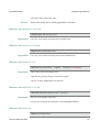
Contents
1 Installation
1.1 Installing on Windows
1
................................... 1
1.2 Installing on Linux . . . . . . . . . . . . . . . . . . . . . . . . . . . . . . . . . . . . . . 4
1.3 Installing the Floating License on Linux . . . . . . . . . . . . . . . . . . . . .
1.3.1 Starting FlexLM Server . . . . . . . . . . . . . . . . . . . . . . . . . . . .
1.3.1.1 Verifying the FlexLM Server . . . . . . . . . . . . . . . .
1.3.1.2 Merging with other licenses managed by FlexLM
6
6
7
8
1.4 Using the Graphical Interface . . . . . . . . . . . . . . . . . . . . . . . . . . . . . . 9
1.5 Using the Command-line Interface . . . . . . . . . . . . . . . . . . . . . . . . . 11
2 Tutorials
15
2.1 Simulate a PN Junction Diode . . . . . . . . . . . . . . . . . . . . . . . . . . . .
2.1.1 Building the Diode Structure . . . . . . . . . . . . . . . . . . . . . . .
2.1.2 Simulating the I-V Characteristics . . . . . . . . . . . . . . . . . . .
2.1.3 Examining the I-V Characteristics . . . . . . . . . . . . . . . . . . .
2.1.4 Visualizing the Solutions . . . . . . . . . . . . . . . . . . . . . . . . . .
2.1.5 Summary . . . . . . . . . . . . . . . . . . . . . . . . . . . . . . . . . . . . . . .
15
15
21
24
27
30
2.2 Simulate a Diode Rectifier Circuit . . . . . . . . . . . . . . . . . . . . . . . . .
2.2.1 Assigning Circuit Symbol . . . . . . . . . . . . . . . . . . . . . . . . . .
2.2.2 Drawing Circuit Schematic . . . . . . . . . . . . . . . . . . . . . . . . .
2.2.3 Simulating the Circuit . . . . . . . . . . . . . . . . . . . . . . . . . . . . .
2.2.4 Summary . . . . . . . . . . . . . . . . . . . . . . . . . . . . . . . . . . . . . . .
31
31
33
35
36
2.3 A 0.18um MOSFET . . . . . . . . . . . . . . . . . . . . . . . . . . . . . . . . . . . .
2.3.1 Building MOSFET Device Structure . . . . . . . . . . . . . . . . .
2.3.2 Simulating I-V Curves . . . . . . . . . . . . . . . . . . . . . . . . . . . .
2.3.3 Setting Mobility Model Parameters . . . . . . . . . . . . . . . . . .
37
37
41
43
2.4 Mix-Mode Simulation of Inverter IO Circuit . . . . . . . . . . . . . . . . . 45
2.4.1 Creating Symbol and Mapping Device Electrode . . . . . . . . 45
2.4.2 Mixed-Mode Simulation . . . . . . . . . . . . . . . . . . . . . . . . . . . 52
2.5 Scripting and Automation . . . . . . . . . . . . . . . . . . . . . . . . . . . . . . . .
2.5.1 Example 1: Curve Plotting . . . . . . . . . . . . . . . . . . . . . . . . .
2.5.2 Example 2: Spreadsheet . . . . . . . . . . . . . . . . . . . . . . . . . . .
2.5.3 Example 3: Building MOSFET Device Structure . . . . . . .
2.5.4 Example 4: Using More Than One Window: . . . . . . . . . . .
2.5.5 Summary . . . . . . . . . . . . . . . . . . . . . . . . . . . . . . . . . . . . . . .
Genius Device Simulator
54
54
56
57
60
62
3
Contents
3 GUI Reference
63
3.1 Device Drawing . . . . . . . . . . . . . . . . . . . . . . . . . . . . . . . . . . . . . . .
3.1.1 Structure Drawing . . . . . . . . . . . . . . . . . . . . . . . . . . . . . . . .
3.1.2 Device and Simulation . . . . . . . . . . . . . . . . . . . . . . . . . . . .
3.1.3 Device View . . . . . . . . . . . . . . . . . . . . . . . . . . . . . . . . . . . .
63
63
67
80
3.2 Device Simulation . . . . . . . . . . . . . . . . . . . . . . . . . . . . . . . . . . . . . . 81
3.2.1 Simulation Setting . . . . . . . . . . . . . . . . . . . . . . . . . . . . . . . . 81
3.3 Circuit Schematics . . . . . . . . . . . . . . . . . . . . . . . . . . . . . . . . . . . . .
3.3.1 Place Circuit Component . . . . . . . . . . . . . . . . . . . . . . . . . .
3.3.2 Simulation Control . . . . . . . . . . . . . . . . . . . . . . . . . . . . . . .
3.3.3 Result Analysis . . . . . . . . . . . . . . . . . . . . . . . . . . . . . . . . . .
3.3.4 Schematics View . . . . . . . . . . . . . . . . . . . . . . . . . . . . . . . . .
89
89
91
96
97
3.4 Device Visualization . . . . . . . . . . . . . . . . . . . . . . . . . . . . . . . . . . . .
3.4.1 View . . . . . . . . . . . . . . . . . . . . . . . . . . . . . . . . . . . . . . . . . .
3.4.2 Draw . . . . . . . . . . . . . . . . . . . . . . . . . . . . . . . . . . . . . . . . . .
3.4.3 Animating the simulation result . . . . . . . . . . . . . . . . . . . .
98
98
99
100
3.5 Spreadsheet . . . . . . . . . . . . . . . . . . . . . . . . . . . . . . . . . . . . . . . . . . 101
3.6 XY Plotting . . . . . . . . . . . . . . . . . . . . . . . . . . . . . . . . . . . . . . . . . . 103
3.7 Text Editor . . . . . . . . . . . . . . . . . . . . . . . . . . . . . . . . . . . . . . . . . .
3.7.1 Search . . . . . . . . . . . . . . . . . . . . . . . . . . . . . . . . . . . . . . . .
3.7.2 Options . . . . . . . . . . . . . . . . . . . . . . . . . . . . . . . . . . . . . . .
3.7.3 Tools . . . . . . . . . . . . . . . . . . . . . . . . . . . . . . . . . . . . . . . . .
4 Programming Reference
111
4.1 Device2D Drawing . . . . . . . . . . . . . . . . . . . . . . . . . . . . . . . . . . . .
4.1.1 Class Device2DScript . . . . . . . . . . . . . . . . . . . . . . . . . . . .
4.1.1.1 Method scriptType . . . . . . . . . . . . . . . . . . . .
4.1.1.2 Method addPolyLineItem . . . . . . . . . . . . . .
4.1.1.3 Method addRegionLabelItem . . . . . . . . . . .
4.1.1.4 Method addRegionDoping . . . . . . . . . . . . . .
4.1.1.5 Method addRegionMoleFraction . . . . . . . .
4.1.1.6 Method addDataset . . . . . . . . . . . . . . . . . . . .
4.1.1.7 Method addDataset . . . . . . . . . . . . . . . . . . . .
4.1.1.8 Method addDopingProfileItem . . . . . . . . .
4.1.1.9 Method addMoleFractionItem . . . . . . . . . .
4.1.1.10 Method addBoundaryItem . . . . . . . . . . . . . .
4.1.1.11 Method addMeshSizeCtrlItem . . . . . . . . . .
4.1.1.12 Method addRulerItem . . . . . . . . . . . . . . . . . .
4.1.1.13 Method addPointItem . . . . . . . . . . . . . . . . . .
4
106
106
108
109
111
111
111
111
111
112
112
112
112
113
113
113
113
113
114
Genius Device Simulator
Contents
Method doMesh . . . . . . . . . . . . . . . . . . . . . . . .
Method exportMesh . . . . . . . . . . . . . . . . . . . .
Method clear . . . . . . . . . . . . . . . . . . . . . . . . .
Method saveToFile . . . . . . . . . . . . . . . . . . . .
Method setTitle . . . . . . . . . . . . . . . . . . . . . .
114
114
114
114
114
4.2 Curve Plot . . . . . . . . . . . . . . . . . . . . . . . . . . . . . . . . . . . . . . . . . . .
4.2.1 PlotScript . . . . . . . . . . . . . . . . . . . . . . . . . . . . . . . . . . . . .
4.2.1.1 Method scriptType . . . . . . . . . . . . . . . . . . . .
4.2.1.2 Method curveGroupCount . . . . . . . . . . . . . .
4.2.1.3 Method curveCountAt . . . . . . . . . . . . . . . . . .
4.2.1.4 Method insertCurveGroup . . . . . . . . . . . . .
4.2.1.5 Method removeCurveGroup . . . . . . . . . . . . .
4.2.1.6 Method setGroupTitle . . . . . . . . . . . . . . . .
4.2.1.7 Method insertCurve . . . . . . . . . . . . . . . . . . .
4.2.1.8 Method clear . . . . . . . . . . . . . . . . . . . . . . . . .
4.2.1.9 Method saveToFile . . . . . . . . . . . . . . . . . . . .
4.2.1.10 Method setTitle . . . . . . . . . . . . . . . . . . . . . .
116
116
116
116
116
116
116
117
117
117
117
117
4.3 SpreadSheet . . . . . . . . . . . . . . . . . . . . . . . . . . . . . . . . . . . . . . . . . .
4.3.1 class SpreadSheetScript . . . . . . . . . . . . . . . . . . . . . . . . . .
4.3.1.1 Method scriptType . . . . . . . . . . . . . . . . . . . .
4.3.1.2 Method getColumnName . . . . . . . . . . . . . . . .
4.3.1.3 Method getColumnData . . . . . . . . . . . . . . . .
4.3.1.4 Method insertRows . . . . . . . . . . . . . . . . . . . .
4.3.1.5 Method insertColums . . . . . . . . . . . . . . . . . .
4.3.1.6 Method setColumnData . . . . . . . . . . . . . . . .
4.3.1.7 Method setColumnName . . . . . . . . . . . . . . . .
4.3.1.8 Method calcColumn . . . . . . . . . . . . . . . . . . . .
4.3.1.9 Method saveToFile . . . . . . . . . . . . . . . . . . . .
4.3.1.10 Method setTitle . . . . . . . . . . . . . . . . . . . . . .
4.3.1.11 Method clear . . . . . . . . . . . . . . . . . . . . . . . . .
118
118
118
118
118
118
118
119
119
119
119
119
120
4.4 MainWindow . . . . . . . . . . . . . . . . . . . . . . . . . . . . . . . . . . . . . . . .
4.4.1 Class MainWindowScript . . . . . . . . . . . . . . . . . . . . . . . . .
4.4.1.1 Method scriptType . . . . . . . . . . . . . . . . . . . .
4.4.1.2 Method openDocumentFromFile . . . . . . . . .
4.4.1.3 Method saveAllToFile . . . . . . . . . . . . . . . .
4.4.1.4 Method newWindow . . . . . . . . . . . . . . . . . . . . .
4.4.1.5 Method getWindowByName . . . . . . . . . . . . . .
4.4.1.6 Method getWindowByNumber . . . . . . . . . . . .
121
121
121
121
121
121
121
122
4.1.1.14
4.1.1.15
4.1.1.16
4.1.1.17
4.1.1.18
Genius Device Simulator
5
Contents
6
Genius Device Simulator
CHAPTER
1 Installation
The VisualTCAD device simulation software works on both Windows and Linux
platform. In the following sections, we shall outline the installation procedures
on both platform, and the procedure to start the graphical user interface and the
command-line interface.
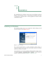
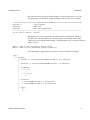
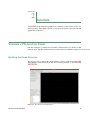
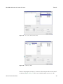
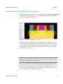
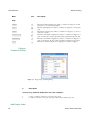
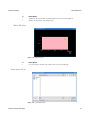
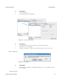
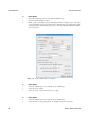
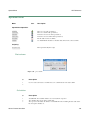
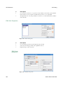
Installing on Windows
The installation package comes as an executable file. Double clicking on it will
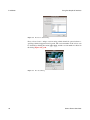
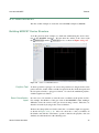
start the installation wizard (Figure 1.1, p. 1).
Figure 1.1 Welcome message.
We recommend install Paraview, a versatile visualization software package, to
examine the output file generated by Genius. The installer of Paraview is included,
and the user can choose to install it.
After installation, we can test the installation with the bundled examples. Please
click Start ⊳ All Programs ⊳ Cogenda Genius TCAD ⊳ VisualTCAD to start the Simulation
manager, and follow the tutorial in Chapter 2, “Tutorials”, p. 15.
Genius Device Simulator
1
Installation
Installing on Windows
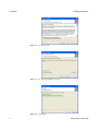
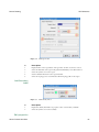
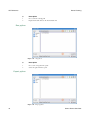
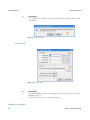
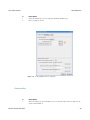
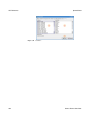
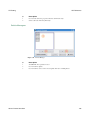
Figure 1.2 License agreement.
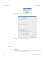
Figure 1.3 Choosing target installation directory.
Figure 1.4 Copying files.
2
Genius Device Simulator
Installing on Windows
Installation
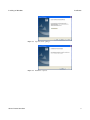
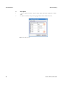
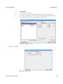
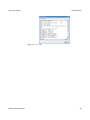
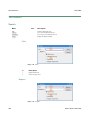
Figure 1.5 Optional software packages.
Figure 1.6 Installation completed.
Genius Device Simulator
3
Installation
Installing on Linux
Installing on Linux
The installation package of the Linux version is a self-extracting program, typically named as Cogenda-Linux-<version>.bin. The same package includes
binaries and data files for several Linux platforms, include Redhat Enterprise
Linux release 5 and release 6, 32- and 64-bit platforms.
Installing
Typically we will run the installer as a super user (root):
$ su
$ ./Cogenda-Linux-1.7.4.bin
The installer will check the operating system and the prerequisite software needed
to run VisualTCAD. If the operating system is recognized, it lists the editions
suitable on this platform in the following menu, along with the features contained
in each edition.
Checking the machine architecture: found rhel5-64
Editions recommended on this machine:
---------------------------------------------------------------------------[ 1] VisualTCAD-flexlm-1.7.4-1-rhel5-64
Platform: rhel5-64
Features: FloatingLicense
---------------------------------------------------------------------------[ 2] VisualTCAD-full-flexlm-1.7.4-1-rhel5-64
Platform: rhel5-64
Features: Full,FloatingLicense
---------------------------------------------------------------------------[ 3] VisualTCAD-full-ib-flexlm-1.7.4-1-rhel5-64
Platform: rhel5-64
Features: Full,InfiniBand,FloatingLicense
---------------------------------------------------------------------------[ 0] Show all editions.
---------------------------------------------------------------------------The user may choose from the menu the edition to be installed. The basic edition
[1] is suitable for most users. The full edition [2] contains advanced products such
as VisualFab and VisualParticle that requires special licenses. The ib edition [3]
only runs on cluster computers with Infiniband interconnect hardware. The user
may also enter 0 to see a full list of editions included in the package.
If the operating system is not recognized, all editions will be displayed, and the
user may choose one that matches his platform most closely.
The installer then prompts the user to input the target installation directory, the
default location is /opt/cogenda.
4
Genius Device Simulator
Installing on Linux
Installation
The end user license agreement will be displayed, and one must enter y to accept
it. It then prints out a summary of this installation, and asks the user to confirm.
========================== Installation Summary ============================
Install to
: /opt/cogenda
Platform
: rhel5-64
Features
: Full,FloatingLicense
---------------------------------------------------------------------------Is the above correct? [Y/exit]
The installer proceeds to unpack the executable binaries and data files. Finally, it
asks the user if a shortcut link is to be created to point to the installed version of the
software. If one accepts the default setting, a soft-link named /opt/cogenda/current
will be created.
Make a link to the installed version? [Y/n]
Enter a name for the installed version [current]
After installation, a typical directory structure would look like the following.
/opt/
|- cogenda/
|- current -> releases/VisualTCAD-flexlm-1.7.4-1-rhel5-64
|
|- previous -> releases/VisualTCAD-flexlm-1.7.4-rhel5-64
|
|- documents/
|
|- 1.7.4/
|
|- ...
|
+- 1.7.4-1/
|
|- ...
|
|- releases/
|
|- VisualTCAD-flexlm-1.7.4-rhel5-64
|
+- VisualTCAD-flexlm-1.7.4-1-rhel5-64
|
|- repo/
|
|- ...
|
|- ...
Genius Device Simulator
5
Installation
Installing the Floating License on Linux
Installing the Floating License on Linux
FlexLM provides floating license, and enable computers in the same network to
share the same license on the license server. When Cogenda software runs on other
machines, they obtain the license from node00 via network. This documents describes how to work with the license manager program, assuming that the license
server runs on the computer node00, and that Cogenda software are installed in a
shared directory /opt/cogenda. It is also assumed that users' home directories
are shared among all hosts with NFS or other distributed file system.
Starting FlexLM Server
Copy the cogenda.lic file to /opt/cogenda/cogenda.lic. The content of the
file looks something like the following
SERVER node00 any
VENDOR COGENDA
USE_SERVER
FEATURE
FEATURE
FEATURE
FEATURE
FEATURE
FEATURE
FEATURE
FEATURE
FEATURE
FEATURE
FEATURE
FEATURE
FEATURE
VTCAD COGENDA 1.000 31-mar-2012 4 SN=Customerxxx SIGN="..."
VFAB COGENDA 1.000 31-mar-2012 4 SN=Customerxxx SIGN="..."
VPTKL COGENDA 1.000 31-mar-2012 4 SN=Customerxxx SIGN="..."
GENIUS_MISC COGENDA 1.000 31-mar-2012 100 SN=Customerxxx SIGN="..."
GENIUS_COMMON COGENDA 1.000 31-mar-2012 32 SN=Customerxxx SIGN="..."
GENIUS_DDM2 COGENDA 1.000 31-mar-2012 32 SN=Customerxxx SIGN="..."
GENIUS_EBM3 COGENDA 1.000 31-mar-2012 32 SN=Customerxxx SIGN="..."
GENIUS_AC COGENDA 1.000 31-mar-2012 32 SN=Customerxxx SIGN="..."
GENIUS_SPICE COGENDA 1.000 31-mar-2012 32 SN=Customerxxx SIGN="..."
GENIUS_OPTICAL COGENDA 1.000 31-mar-2012 32 SN=Customerxxx SIGN="..."
GENIUS_HIDDM1 COGENDA 1.000 31-mar-2012 32 SN=Customerxxx SIGN="..."
GDS2MESH COGENDA 1.000 31-mar-2012 32 SN=Customerxxx SIGN="..."
GSEAT COGENDA 1.000 31-mar-2012 32 SN=Customerxxx SIGN="..."
Each line corresponds to a feature. This file shows a license with all features
enabled, with 32-way parallel computation enabled in the Genius simulator.
One first enter the Cogenda environment with the command below.
$ source /opt/cogenda/1.7.3/bin/setenv.sh
One then starts the license server with the following command on node00. It is
not necessary to use root privilege.
$ lmgrd -c /opt/cogenda/cogenda.lic -l /tmp/flexlm.log
6
Genius Device Simulator
Installing the Floating License on Linux
Installation
The lmgrd command starts the FlexLM server, read in the license file, saves the
log messages to /tmp/flexlm.log, and turned to background running. If the
server is correctly started, the end of flexlm.log file should contain the followings.
14:07:56
14:07:56
14:07:56
14:07:56
14:07:56
14:07:56
14:07:56
14:07:56
14:07:56
14:07:56
14:07:56
14:07:56
(lmgrd) License file(s): /opt/cogenda/cogenda.lic
(lmgrd) lmgrd tcp-port 27000
(lmgrd) Starting vendor daemons ...
(lmgrd) Started COGENDA (internet tcp_port 48793 pid 19111)
(COGENDA) FLEXnet Licensing version v11.10.0.0 build 95001 x64_lsb
(COGENDA) Server started on localhost for: VTCAD
(COGENDA) VFAB VPTKL GENIUS_MISC
(COGENDA) GENIUS_COMMON GENIUS_DDM2 GENIUS_EBM3
(COGENDA) GENIUS_AC GENIUS_SPICE GENIUS_OPTICAL
(COGENDA) GENIUS_HIDDM1 GDS2MESH GSEAT
(COGENDA) EXTERNAL FILTERS are OFF
(lmgrd) COGENDA using TCP-port 48793
The license server is running on TCP port 27000 of node00.
Verifying the FlexLM Server
Usually Cogenda software will automatically find the license server running on the
local network, but it is advised to explicitly configure the location of the license
server. One creates a config file .flexlmrc under his/her home directory, i.e.
$HOME/.flexlmrc. The content of the file would be
COGENDA_LICENSE_FILE=@node00
One can use the lmstat command to verify if one can successfully query the
license server. For example, one can run the command on node03, and expect
the following output:
$ lmstat
lmstat - Copyright (c) 1989-2011 Flexera Software, Inc. All Rights Reserved.
Flexible License Manager status on Thu 1/5/2012 14:17
License server status: 27000@node00
License file(s) on hydrogen: /opt/cogenda/cogenda.lic:
node00: license server UP (MASTER) v11.10
Genius Device Simulator
7
Installation
Installing the Floating License on Linux
Vendor daemon status (on hydrogen):
COGENDA: UP v11.10
Finally, one can use the lmdown command.
Merging with other licenses managed by FlexLM
If one is using FlexLM licenses issued by other vendor as well as that from Cogenda, he/she can manage them with a single instance of FlexLM server.
To do this, one needs to copy all "Vendor Daemons" from all vendors, along with
the lmgrd program, to the same directory, i.e. /opt/flexlm/bin. Cogenda's
vendor daemon is located at /opt/cogenda/1.7.3/bin/COGENDA.
One then copies all the license files to /opt/flexlm/license/, and starts the
flexlm server with the command.
$ /opt/flexlm/bin/lmgrd -l /tmp/flexlm.log \
-c /opt/flexlm/license/cogenda.lic:/opt/flexlm/license/synopsys.lic
Note how license files from various vendors are concatenated with semicolon in
the -c option.
8
Genius Device Simulator
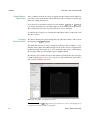
Using the Graphical Interface
Installation
Using the Graphical Interface
VisualTCAD is the integrated graphical user interface of the Genius device simulation package.
To start VisualTCAD in Windows, please click Start ⊳ All Programs ⊳ Cogenda Genius TCAD ⊳
VisualTCAD in the Start Menus.
In Linux, one types the following command in a shell.
$ /opt/cogenda/1.7.2/VisualTCAD/bin/VisualTCAD &
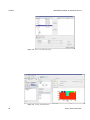
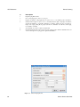
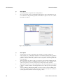
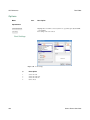
The main window of VisualTCAD is shown in Figure 1.7, p. 9.
Figure 1.7 The VisualTCAD Main Window
Checking
License Status
Genius Device Simulator
To check the license status, click in the menu Help ⊳ License . The license status
dialog shown in Figure 1.8, p. 10. If you download the trial version of Genius
from the website, the default license file included in the package is valid for one
month only. Some advanced features and disabled and at most 2 processors are
supported. You need to register your copy with Cogenda in order to continue using
Genius. To register, click the register button, and email the generated registration
code to Cogenda or a sales representative.
9
Installation
Using the Graphical Interface
Figure 1.8 The License Status Dialog
Every release bears a unique version string, which should be quoted when requesting technical support from Cogenda. The version number of the release can
be checked by clicking the menu Help ⊳ About , and the version number is shown in
the dialog Figure 1.9, p. 10.
Figure 1.9 The About Dialog
10
Genius Device Simulator
Using the Command-line Interface
Installation
Using the Command-line Interface
This section outlines the command-line usage of Genius under Linux. A similar
command-line interface exists under Windows, but is rarely used.
Configuration
After the installation, one may want to test the installation with the following steps.
Daily usage can be (and usually should be) performed under a normal user account,
instead of using the root account.
We first copy the examples to our home directory:
$ cp -r /opt/cogenda/genius/examples $HOME/genius_examples
$ cd $HOME/genius_examples/PN_Diode/2D
For convenience, we add the installation directory to his PATH environment for
his convenience. With the bash shell one can type
$ export PATH=$PATH:/opt/cogenda/genius/bin
or with csh
# set PATH=$PATH:/opt/cogenda/genius/bin
Now we try running the PN diode example with one single processor:
$ genius -n 4 -i pn2d.inp
Running with
one CPU
The running log will be output to screen. It is pretty long, we show only the
beginning and ending portions here:
*************************************************************************
*
888888
88888888
88
888 88888
888
888
8888888
*
*
8
8
8
8 8
8
8
8
8
8
*
* 8
8
8 8
8
8
8
8
8
*
* 8
88888888
8
8
8
8
8
8
888888
*
* 8
8888 8
8
8 8
8
8
8
8
*
*
8
8
8
8
8 8
8
8
8
8
*
*
888888
88888888 888
88
88888
8888888
8888888
*
*
*
* Parallel Three-Dimensional General Purpose Semiconductor Simulator
*
Genius Device Simulator
11
Installation
Using the Command-line Interface
*
*
* This is Genius Commercial Version 1.7.2 with double precision.
*
*
*
*
Copyright (C) 2008-2011 by Cogenda Company.
*
*************************************************************************
Constructing Simulation System...
External Temperature = 3.000000e+02K
Setting each voltage and current source here...done.
...
...
DC Scan: V(Anode) = 2.000000e+00 V
----------------------------------------------------------------------------its
| Eq(V) | | Eq(n) | | Eq(p) | | Eq(T) | |Eq(Tn)| |Eq(Tp)| |delta x|
----------------------------------------------------------------------------0
3.69e-03 4.42e-05 5.79e-05 0.00e+00 0.00e+00 0.00e+00 0.00e+00
1
7.67e-11 3.89e-06 3.07e-06 0.00e+00 0.00e+00 0.00e+00 4.93e-02
2
7.98e-15 3.44e-07 3.55e-07 0.00e+00 0.00e+00 0.00e+00 2.87e-03
3
2.57e-15 3.47e-08 3.52e-08 0.00e+00 0.00e+00 0.00e+00 2.87e-04
4
1.97e-15 4.09e-09 2.72e-09 0.00e+00 0.00e+00 0.00e+00 2.11e-05
5
1.92e-15 5.06e-10 1.68e-10 0.00e+00 0.00e+00 0.00e+00 1.09e-06
----------------------------------------------------------------------------CONVERGED_PNORM_RELATIVE
Write System to XML VTK file pn2d.vtu...
Write System to CGNS file pn2d.cgns...
Write Boundary Condition to file bc.inc...
Genius finished. Totol time is 1 min 2.78475 second. Good bye.
Running with
Multiple CPUs
We can run Genius with more than one CPUs, using the -n option to specify the
number of CPUs to utilize.
$ genius -n 2 -i pn2d.inp
Registering
12
If you download the trial version of Genius from the website, the default license
file included in the package is valid for one month only. Some advanced features
and disabled and at most 2 processors are supported. You need to register your
copy with Cogenda in order to continue using Genius. To register, simply type
Genius Device Simulator
Using the Command-line Interface
Installation
$ genius -r
and a registration code will be displayed on screen.
*************************************************************************
To register your copy, email the following registration code:
81e434677a0bb0501aabd85d07b9f621feb19ba6ca5f24ff987e583fa083b48a771796178
ac1d9de40cc53f2980fd12de936febdcadb16e3b66b08e9e0bd314fc511f63cd2264b9ab1
b10635ad3a515ec4f62e101d86206fd7694ae938210d0a406eda6bece9b760f28f916c88d
d83010470068fe55afbcdff8da09c4aed0d9d
Please email this registration code to Cogenda or its redistributors. You will be
given the license file lic.dat. Copy it to
/opt/cogenda/genius/license/lic.dat
and overwrite the old file. Genius now should work under registered mode, with
all options you subscribed turned on.
Command
Line Options
The command line options for Genius are listed below:
Name
genius
-- Genius 3D parallel simulator
Synopsis
genius [ -n ncpus ]
genius -r
-i filename
Options
Genius Device Simulator
-n ncpus
Number of processors to be used in the simulation
-i filename
Input file to the simulator
-r
Register the copy with Cogenda
13
Installation
14
Using the Command-line Interface
Genius Device Simulator
CHAPTER
2 Tutorials
VisualTCAD is the integrated graphical user interface of the Genius device simulation package. This chapter provides a step-by-step tutorial to the VisualTCAD
graphical user interface.
Simulate a PN Junction Diode
Our first attempt is to simulate the forward I-V characteristics of a short-base PN
junction diode. The files of this tutorial are located at VisualTCAD/examples/tutorial/tu
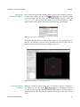
Building the Diode Structure
The first step is to construct the diode structure. Choose in the menu File ⊳ New
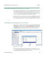
Device Drawing , which will start the 2D device drawing window, as shown in Figure 2.1, p. 15.
Figure 2.1 The 2D Device Drawing Window
Genius Device Simulator
15
Tutorials
Simulate a PN Junction Diode
Simple Mouse
Operations
The coordinates of the mouse cursor is displayed in the status bar at the right-bottom corner of the main window. The default unit of the coordinates is micron, but
this can be changed by the user.
To zoom-in or zoom-out the viewport, one can click the
Zoom-in or
Zoom-out
tool button. Alternatively, one could simple scroll the mouse wheel up or down.
The zooming will leave the view under the mouse cursor stationary.
To translate the viewport, one can hold the mid-button (wheel) of the mouse and
drag the viewport.
Drawing
Device Outline
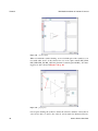
We start by drawing a box representing the body of the silicon diode. Choose from
the drawing tools
Add Rectangle .
We define the first corner of the rectangle by clicking at the coordinates (-1, 0).
One may notice that in the Add Rectangle tool, the mouse cursor is snapped to the
background grip. 1Click again at (1, -2) to define the other corner, and complete
the rectangle. This closed rectangle region is slightly shaded.
We then proceed to define the anode and cathode by drawing the two rectangles
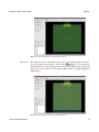
(-0.2,0.2)-(0.2,0) and (-1,-2)-(1,-2.2), respectively. The outline of the device structure is shown in Figure 2.2, p. 16.
Figure 2.2 The Outline of the PN Junction Diode
1
16
The default snap mode is
Auto-Snap , which is appropriate in most occasions. The snapping modes
are described in detail in a separate documentation.
Genius Device Simulator
Simulate a PN Junction Diode
Assigning
Material Regions
Tutorials
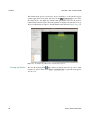
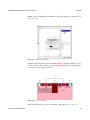
Every enclosed region in the drawing must be labelled and assigned a material.
To label such a region, one chooses the
Add Region Label tool, and click within
one of the regions. We first click at (0, -1), which prompts a dialog as shown in
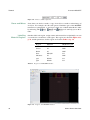
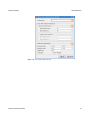
Figure 2.3, p. 17. We key in the label Silicon, the maximum mesh size of 0.1
micron in this region, choose the Si material from the list, and click OK.
Figure 2.3 Device Region Label Dialog
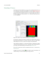
One notices that the region is now filled with the pink color representing the silicon
material. We similarly assign the Anode and Cathode regions, both of the Al
material, and the drawing becomes as in Figure 2.4, p. 17.
Figure 2.4 The Regions of the PN Junction Diode
Placing Doping
Profiles
Genius Device Simulator
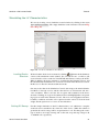
Doping is essential for semiconductor devices to function. To place a doping profile to the device, one chooses the
Add Doping Profile tool. A doping box consists
of a baseline and a height, and the available doping functions include uniform,
Gaussian and Erf. We first place the uniform body doping in the entire silicon
region.
17
Tutorials
Simulate a PN Junction Diode
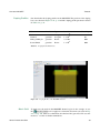
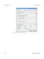
In the Doping Profile state, we click first at (-2,0) and then at (2,0) to define the
baseline, and finally click at (2,-2) to define the height of the doping box. A menu
pops up and ask for the doping function, where we choose Uniform Doping Profile
in this case. A dialog pops up for us to key in the doping profile parameters, as
shown in Figure 2.5, p. 18. We shall name the profile body, and a n-type doping
concentration of 1 × 1016 cm3 .
Figure 2.5 Uniform Doping Profile Dialog
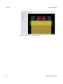
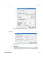
The p-type diffusion is then defined. We draw another doping box with baseline
(-0.2,0)-(0.2,0) and height to (0.2,-0.2). We choose the Gaussian doping function
and in the dialog shown in Figure 2.6, p. 18, we key in the peak concentration
1 × 1019 cm3 , and the characteristic length 0.1μm.
Figure 2.6 Gaussian Doping Profile Dialog
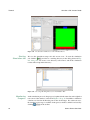
The final doping profile of the diode is shown in Figure 2.7, p. 19. Note the
different color representing the n- and p-type doping profiles.
18
Genius Device Simulator
Simulate a PN Junction Diode
Tutorials
Figure 2.7 The Doping Profiles of the PN Junction Diode
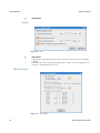
Meshing
The numerical device simulation always relies on a mesh grid that divides the
device into many small elements. Click on the
Do Mesh tool, and accepts the
default parameters in the mesh parameter dialog. The initial mesh is shown in
Figure 2.8, p. 19. One may notice that the PN junction is slightly highlighted
with shading.
Figure 2.8 The Initial Mesh Grid of the PN Junction Diode
Genius Device Simulator
19
Tutorials
Simulate a PN Junction Diode
This initial mesh grid is not ideal for device simulation, as the junction region
would require finer mesh grids. One may use the
Mesh Refinement tool to refine
the initial mesh. Accepting the default refine parameters, one sees the mesh is
refined at the junction region, where the gradient of doping concentration is steep.
We do 2 refinements in sequence, and the final mesh is shown in Figure 2.9, p. 20.
Figure 2.9 The Final Refined Mesh Grid of the PN Junction Diode
Saving the Device
20
We save the drawing with
Save , and key in the file name diode.drw. Additionally, we choose in the menu Device ⊳ Save Mesh to File to export the mesh grid to
diode.tif.
Genius Device Simulator
Simulate a PN Junction Diode
Tutorials
Simulating the I-V Characteristics
We start by creating a new simulation control window by clicking in the menu
File ⊳ New Device Simulation . The empty simulation control window is shown in Figure 2.10, p. 21.
Figure 2.10 The Device Simulation Control Window
Loading Device
Structure
We first load the diode device structure by clicking
Load button in the Summary
section of the simulation control window. We select the diode.tif file we just
created. It takes a few seconds for VisualTCAD and Genius to analyse the tif file.
When it finishes, the device structure is visualized in the Structure Viewer, and
the automatically identified device electrodes are listed in the Electrodes section.
In this case we have the Anode and the Cathode.
One may notice that in the Simulation Control dock widget, the default Simulation Mode is Steady-state, and the other choices are Transient and Circuit-element. There is also the list of regions and boundaries in the device
structure. Clicking on a region or boundary name would highlight the corresponding region or label in the Structure Viewer. The user can setup physical models,
boundary conditions and other solver options from the various tools in the dock
widget, but the options are too vast to be described here.
Setting DC Sweep
Genius Device Simulator
For this simple simulation of the I-V characteristics, it is sufficient to setup the
electrical sources attached to the electrodes of the device. While the cathode is
grounded, the anode voltage will be swept from 0 to 1 volt. We change the source
type of anode to Voltage Sweep, and set the start, stop and step voltages to 0,
1, and 0.05 volt, respectively.
21
Tutorials
Simulate a PN Junction Diode
Figure 2.11 The Structure and Electrodes of the Simulated Device
Starting
Simulation Job
We save the simulation setup to the file diode.sim. To start the simulation
Run and choose a working directory in the dialog shown in Figjob, click the
ure 2.12, p. 22. We create a new directory called run1, and all the simulation
results will be kept in this directory.
Figure 2.12 Choosing a Working Directory for the Simulation Run
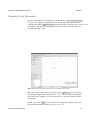
Monitoring
Progress
22
As the simulation proceeds, the progress is updated in the status bar, at the right-bottom corner of the window, as shown in Figure 2.13, p. 23. In addition, simulation
solutions are listed in the Results pane in the dock widget. For advanced users,
the running log message is available in the process monitor, which is activated by
clicking
Console in the toolbar.
Genius Device Simulator
Simulate a PN Junction Diode
Tutorials
Figure 2.13 The Device Simulation in Progress
Genius Device Simulator
23
Tutorials
Simulate a PN Junction Diode
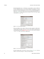
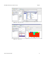
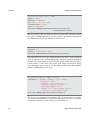
Examining the I-V Characteristics
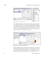
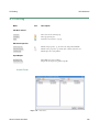
Opening the
Spreadsheet
After the simulation completes, we wish to plot the I-V characteristics of this forShow IV Data button to open
ward-biased PN junction diode. We can click the
the spreadsheet containing the terminal information of the solutions. The spreadsheet is shown in Figure 2.14, p. 24.
Figure 2.14 Spreadsheet of the Simulated Terminal Characteristics
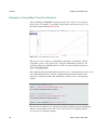
Plotting the
I-V Curve
We first select the columns Anode_Vapp and Anode_current. As in most GUI
applications, one can select multiple columns by clicking on the column header
and holding the Control key. When the two columns are selected, right-click to
activate the context menu, and choose to plot the data using as the Anode_Vapp
x-variable, as shown in Figure 2.14, p. 24. The plot appears in a new plot window,
as shown in Figure 2.15, p. 25.
Setting Plot
Options
To change the axes settings, click Edit Axes in the dock widget. In the axes property
dialog shown in Figure 2.16, p. 25, select the Left y-axis and key in the title,
scale and range of the axis.
To change the curve plotting settings, select the curve name from the list in the
dock widget, and click Edit Legend . In the dialog window shown in Figure 2.17,
p. 25, set the line and symbol options.
The final plot is shown in Figure 2.18, p. 26.
24
Genius Device Simulator
Simulate a PN Junction Diode
Tutorials
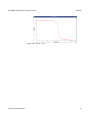
Figure 2.15 Diode I-V Characteristics in Linear Scale
Figure 2.16 Axis Property Dialog
Figure 2.17 Plot Style Dialog
Genius Device Simulator
25
Tutorials
Simulate a PN Junction Diode
Figure 2.18 Diode I-V Characteristics in Log Scale
26
Genius Device Simulator
Simulate a PN Junction Diode
Tutorials
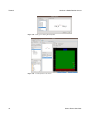
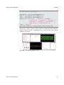
Visualizing the Solutions
We switch back to the Simulation Control window, and in the Result list, we select
all solutions. Right-click and in the context menu click Open Visualization ⊳. A new
visualization window is opened.
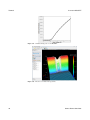
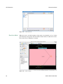
Suppose we want to plot the electron concentration profile in the device, choose in
the menu Draw ⊳ Draw Pseudo Color Electron density . In the visualization window, one
can hold the left mouse button and drag in the visualization window. Scrolling
the mouse wheel would zoom-in or -out the view, and dragging with the middle button (wheel button) would pan the view. As shown in Figure 2.19, p. 27,
the electron concentration is represented by the color scale. Check in the menu
Options ⊳ Signed Log Scale to enable the log scale for the z axis.
Figure 2.19 Electron Concentration in the Silicon Region of the Diode
Filter
One can filter the areas to be included or excluded in the visualization, in the Mesh
Filter section in the dock widget. We choose to filter by region names, as shown
in Figure 2.19, p. 27.
Animation
We have included all the solutions in the visualization, each solution at a different
anode voltage. The electron profile is different for each solution. In the Animation
Control section of the dock widget, we can step through the solutions by clicking
the
Next and
Previous buttons.
Genius Device Simulator
27
Tutorials
Simulate a PN Junction Diode
Figure 2.20 Animation Control
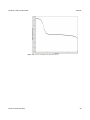
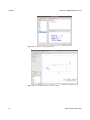
Probe
We can probe the hole concentration along the straight line (0,0)-(0,-2) in the Probe
section in the dock widget, as shown in Figure 2.21, p. 28. After clicking the
Probe button, a spreadsheet containing the interpolated values of hole concentration is opened. We can then plot the hole concentration along the cut-line, as
shown in Figure 2.22, p. 29.
Figure 2.21 Probe Control
28
Genius Device Simulator
Simulate a PN Junction Diode
Tutorials
Figure 2.22 Hole Concentration Along the Probe Line
Genius Device Simulator
29
Tutorials
Simulate a PN Junction Diode
Summary
In the preceding sections, we went through the steps of simulating the I-V characteristics of an PN junction diode. This illustrates the basic flow of device simulation in VisualTCAD.
30
Genius Device Simulator
Simulate a Diode Rectifier Circuit
Tutorials
Simulate a Diode Rectifier Circuit
We can combine the semiconductor device simulation with SPICE circuit simulation. This section shows the steps to demonstrate the rectifying effect of the PN
diode. The files of this tutorial are located at VisualTCAD/examples/tutorial/tut2.
Assigning Circuit Symbol
We open the simulation file diode.sim again, and change the Simulation Mode
to Circuit-element. Since this is a two-terminal device, the default circuit
symbol with two pins is displayed, as shown in Figure 2.23, p. 31.
Figure 2.23 Default Symbol for the Two-Terminal Device
We want a more suitable symbol for the diode, so we click Change Symbol, and
in the dialog (Figure 2.24, p. 32), we choose the diode symbol.
Then we must map the two device electrodes to the two pins in the circuit symbol,
as shown in Figure 2.25, p. 32. We save to another file named diode-circuit.sim.
Genius Device Simulator
31
Tutorials
Simulate a Diode Rectifier Circuit
Figure 2.24 Dialog for Selecting Circuit Symbol
Figure 2.25 Circuit Symbol for the Diode
32
Genius Device Simulator
Simulate a Diode Rectifier Circuit
Tutorials
Drawing Circuit Schematic
We proceed to draw the circuit schematic. Click in the menu File ⊳ New Circuit Schematic
to open a new schematic capturing window. We first place the numerical device
component by clicking Numerical Device in the dock widget. Select diode-circuit.sim
in the dialog. The diode symbol appears at the mouse cursor and can be placed to
the schematic with a click.
Figure 2.26 Placing the Semiconductor Diode Device Model in the circuit
The other symbol components can be placed using
Component tool, the dialog
for selecting components is shown in Figure 2.27, p. 34. For common components
like resistors and capacitors, one can alternatively use the shortcut buttons in the
dock widget.
Finally one use the
Wire tool to connect the components together. The completed circuit schematic is shown in Figure 2.28, p. 34.
Genius Device Simulator
33
Tutorials
Simulate a Diode Rectifier Circuit
Figure 2.27 Dialog for Selecting Components
Figure 2.28 The Completed Rectifier Circuit Schematic
34
Genius Device Simulator
Simulate a Diode Rectifier Circuit
Tutorials
Simulating the Circuit
We want to do transient mode simulation, so we setup the timing with the
tool, as shown in Figure 2.29, p. 35.
Setup Simulation
Figure 2.29 Dialog for Setting Up Transient Analysis
We click the
Run Simulation tool to start the simulation. The monitoring and
analysis procedure is similar to that in the previous example. In the result spreadsheet, we plot the columns probe1pos and v1pos, using time as the x-variable.
The waveform plot is shown in the Figure 2.30, p. 35.
Figure 2.30 The Voltage of the Sine Source and the Voltage Probe, as Functions of Time
Genius Device Simulator
35
Tutorials
Simulate a Diode Rectifier Circuit
Summary
In this section, we outlined the procedure of simulating devices in circuit. This
integrated approach allows one to combine the accuracy of device simulation with
the power of SPICE circuit simulation.
36
Genius Device Simulator
A 0.18um MOSFET
Tutorials
A 0.18um MOSFET
The files of this example are located at VisualTCAD/examples/MOSFET.
Building MOSFET Device Structure
As in the previous diode example, we shall start with drawing the device structure of the MOSFET transistor. We first draw the outline of the device with
the Add Rectangle and the
Add Polyline tools, as shown in Figure 2.31, p. 37.
Figure 2.31 Outline of a MOSFET transistor.
Polyline Tool
To draw a polyline or polygon, one can use the polyline tool. Single-click to add a
point to the line, double-click to add the last point of the line. If the first point and
the last point coincide, a polygon is formed. To cancel the unfinished polyline,
click the right mouse button.
Exact Coordinates
Input
In some cases, it is desirable to enter the exact coordinates of the points of a line.
For example, the thickness of the gate oxide of this MOSFET is 4nm, making it
difficult to locate the corners of the gate electrode using a mouse. Therefore, we
draw the electrode by keying in the exact coordinates.
We first enter the polyline tool. In the status bar, a coordinates input area appears,
as shown in Figure 2.32, p. 38. After one enters the x- and y-coordinates in
the blanks, and click the enter button, a point is added to the polyline. One can
similarly use this function in other drawing tools.
Genius Device Simulator
37
Tutorials
A 0.18um MOSFET
Figure 2.32 Exact coordinates input area.
Clone and Mirror
Some times one desire to make a copy of an object, or make a mirror image of
an object. For example, the side-wall spacers around the gate of the MOSFET
transistor are symmetrical, so one hope to draw one of them and make the other
by mirroring. The
Clone ,
MirrorX and
MirrorY tools can help you on these
tasks.
Labelling
Material Regions
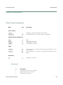
One then label each region, assign a name and a material to it. Optionally, one can
set a mesh-size constraint to each region. The regions are shown in Figure 2.33,
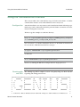
p. 38, and the parameters for the regions are listed in Table 2.1, p. 38.
Region
Material
Mesh Size / μm
substrate
Source
Drain
Gate
Substrate
spc1
spc2
Silicon
Al
Al
NPolySi
Al
Nitride
Nitride
0.05
0.04
0.04
0.1
0.05
0.1
0.1
Table 2.1 Regions of the MOSFET transistor.
Figure 2.33 Regions of the MOSFET transistor.
38
Genius Device Simulator
A 0.18um MOSFET
Doping Profiles
Tutorials
One then define the doping profiles in the MOSFET. The position of the doping
boxes are shown in Figure 2.34, p. 39 and the doping profile parameters shown
in Table 2.2, p. 39.
Name
Substrate
Channel
LDD_S/LDD_D
Source/Drain
Profile
uniform
gaussian
gaussian
gaussian
Type
Acceptor
Acceptor
Donor
Donor
Peak Conc. / cm−3
16
5 × 10
1 × 10¹⁸
2 × 10¹⁹
1 × 10²⁰
Char. L / μm
0.1
0.02
0.04
Table 2.2 Doping Profiles Parameters.
Figure 2.34 Doping Profiles of the MOSFET transistor.
Mesh Grid
Genius Device Simulator
To make sure the mesh in the MOSFET channel region is fine enough, we use
the
Mesh size constrain tool to apply two constraints, shown in cyan color in Figure 2.35, p. 40. After two refinements, the final mesh is generated. We save the
mesh to a.tif file for further simulations.
39
Tutorials
A 0.18um MOSFET
Figure 2.35 Final mesh grid of the MOSFET transistor.
40
Genius Device Simulator
A 0.18um MOSFET
Tutorials
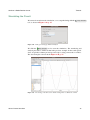
Simulating I-V Curves
As in the previous diode simulation, we create a device simulation and load the.tif
file containing the mesh grid of the MOSFET. As shown in Figure 2.36, p. 41,
we are in the steady-state simulation mode, the source and substrate terminals are
grounded. The drain terminal is connected to a constant voltage source of 0.1 V.
We shall sweep the gate terminal from 0 to 2 V to obtain the transfer characteristics of the MOSFET.
Figure 2.36 Simulation setup for calculating the Id-Vg curve of the MOSFET.
We submit the simulation for running, and shall observe that the drain voltage is
first ramped up from 0 to0.1 V, before the actual gate voltage scan begins. This
drain ramp-up is necessary to ensure the convergence of the simulation.
After running the simulation, we obtain the spreadsheet containing the terminal
voltage/current information in the sweep. We plot the drain current against the
gate voltage, and obtain the Id-Vg curve shown in Figure 2.37, p. 42.
One can also visualize the electron concentration in the device, as shown in Figure 2.38, p. 42.
It might be interesting to click the
Play tool-button to play the animation, and
watch the change of electron density as gate voltage increases.
Genius Device Simulator
41
Tutorials
A 0.18um MOSFET
Figure 2.37 Simulated Id-Vg curve of the MOSFET.
Figure 2.38 Electron concentration at Vg=0.45V.
42
Genius Device Simulator
A 0.18um MOSFET
Tutorials
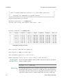
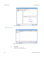
Setting Mobility Model Parameters
So far we have always been using the default physical models and material parameters. In practice, we often need to modify these parameters to model certain
aspects of the real device more accurately. VisualTCAD allows you to modify
models and parameters in material regions and at boundaries.
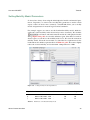
For example, suppose we want to use the Lombardi mobility model, which describes the carrier mobility in the inversion layer more accurately. We click the
Physical Model tool button, and in the material models tab of the physical model
dialog (Figure 2.39, p. 43), we select the substrate region. Since this is a semiconductor region, we can choose the mobility model of it. We select the Lombardi
mobility model. From the user manual, we found the list of parameters for the
Lombardi model, which is reproduced here in Table 2.3, p. 43. We want to slightly
reduce the electron mobility, and set the MUN2.LSM parameter to 1400.
Figure 2.39 Setting mobility model and parameters.
Symbol
Parameter
Unit
Si:n
Si:p
𝛼
𝛽
𝜁
EXN1.LSM / EXP1.LSM
EXN2.LSM / EXP2.LSM
EXN3.LSM / EXP3.LSM
-
0.680
2.0
2.5
0.719
2.0
2.2
Table 2.3 Parameters of Lombardi mobility model
Genius Device Simulator
43
Tutorials
A 0.18um MOSFET
Symbol
Parameter
Unit
Si:n
Si:p
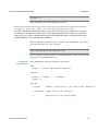
𝜆
𝛾
𝜇0
𝜇1
𝜇2
𝑃𝑐
𝐶𝑟
𝐶𝑠
𝐵
𝐶
𝐷
𝑣sat0
𝛽
𝛼
EXN4.LSM / EXP4.LSM
EXN8.LSM / EXP8.LSM
MUN0.LSM / MUP0.LSM
MUN1.LSM / MUP1.LSM
MUN2.LSM / MUP2.LSM
PC.LSM
CRN.LSM / CRP.LSM
CSN.LSM / CSP.LSM
BN.LSM / BP.LSM
CN.LSM / CP.LSM
DN.LSM / DP.LSM
VSATN0 / VSATP0
BETAN / BETAP
VSATN.A / VSATP.A
-
0.125
2.0
52.2
43.4
1417.0
0 (fixed)
9.68 × 10¹⁶
3.43 × 10²⁰
4.75 × 10⁷
1.74 × 10⁵
5.82 × 10¹⁴
2.47
2.0
0.8
0.0317
2.0
44.9
29.0
470.5
9.23 × 10¹⁶
2.23 × 10¹⁷
6.10 × 10²⁰
9.93 × 10⁶
8.84 × 10⁵
2.05 × 10¹⁴
2.47
1.0
0.8
-
cm2 V−1 s−1
cm2 V−1 s−1
cm2 V−1 s−1
cm−3
cm−3
cm−3
cm/s
cm/s
Table 2.4 Parameters of Lombardi mobility model
We can now run the simulation again, and observe the change to the Id-Vg curve,
as a result of the change in the mobility model.
44
Genius Device Simulator
Mix-Mode Simulation of Inverter IO Circuit
Tutorials
Mix-Mode Simulation of Inverter IO Circuit
As in the previous cmos simulation, we can create a device structure of inverter
and do Mix-Mode simulation. So we need draw a structure of inverter, the detail
step refer to mosfet structure building(“Building MOSFET Device Structure”,
p. 37), here we omit the drawing structure step. About this example we need draw
a inverter symbol, then use VisuaTCAD to do Mix-Mode simulation.
We can combine the semiconductor device simulation with SPICE circuit simulation. This section shows the steps to demonstrate the output characteristic of Inverter. The files of this tutorial are located at VisualTCAD/examples/Inverter.
Creating Symbol and Mapping Device Electrode
The first step is to draw the symbol of Inverter. Choose in the menu File ⊳ New
Circuit Schematic , then choose in the menu Place ⊳ Library Manager which will start the
Library drawing window, as shown in Figure 2.40, p. 45. Click the child window
Add Library , input the Library name inverter, and last click to add symbol.
Figure 2.40 draw new symbol
Now we can obtain the child window of drawing symbol, as shown in Figure 2.41,
p. 46. First input the symbol name, then add the line or circles, in the process user
can using Enable/disabled grid snapping mode as needed.
Genius Device Simulator
45
Tutorials
Mix-Mode Simulation of Inverter IO Circuit
Figure 2.41 inverter symbol
When we finish the symbol drawing, we need add the pin of the symbol to connect with other device of the circuit, here we need 4 pins, named PIN_VDD,
PIN_GND, PIN_IN, PIN_OUT, the pin name is must begin with PIN_. the drawing process and is shown in Figure 2.42, p. 46.
Figure 2.42 pin property
Last step for drawing the symbol is define the reference attribute. About the inverter device here we choose the value N, and it stands for Numerical Device.
46
Genius Device Simulator
Mix-Mode Simulation of Inverter IO Circuit
Tutorials
Which can use in Mix-Mode simulation. The child window is shown in Figure 2.43, p. 47.
Figure 2.43 editing symbol attribute
Our 2D inverter structure is shown in Figure 2.44, p. 47. Here total have 8 electrodes, we need connect each 2 electrodes like Figure 2.44, p. 47, finally we have
4 electrodes as our symbol of inverter.
Figure 2.44 2D inverter structure
before the interconnect, we need do boudary setting like Figure 2.45, p. 48
Genius Device Simulator
47
Tutorials
Mix-Mode Simulation of Inverter IO Circuit
Figure 2.45 boundary parameter setting
Aboout Numerical simulation, as shown in Figure 2.46, p. 48. We use interconnect command to connect each 2 electrodes, such as connectting PSub to PSource,
connectting PGate to NGate, connectting PDrain to NDrain and connectting NSub
to NSource. It is shown in Figure 2.47, p. 49. At the same time we need define
the new electrode as VDD, IN, OUT and GND. it is shown in Figure 2.48, p. 49.
The new electrode OUT ia attached to current source so choosing Interconnect
Floating setting is true, as shown in Figure 2.49, p. 50.
Figure 2.46 boudary Condition and Interconnect
When we finish the boudary setting and interconnect setting, we need change the
Simulation Mode to Circuit Element, Since this is a four-terminal device, the default circuit symbol with four pins is displayed, as shown in Figure 2.50, p. 50.
We want a more suitable symbol for the inverter, so we click Change Symbol, we
change the symbol to we have edited before, as shown in Figure 2.51, p. 51.
48
Genius Device Simulator
Mix-Mode Simulation of Inverter IO Circuit
Tutorials
Figure 2.47 choose the contact to interconnect
Figure 2.48 define new contact
Then we must map the four device electrodes to the four pins in the circuit symbol,
as shown in Figure 2.52, p. 51. We save to the file named inverter.sim.
Genius Device Simulator
49
Tutorials
Mix-Mode Simulation of Inverter IO Circuit
Figure 2.49 Interconnect Floating setting
Figure 2.50 Change Simulation Mode
50
Genius Device Simulator
Mix-Mode Simulation of Inverter IO Circuit
Tutorials
Figure 2.51 change symbol setting
Figure 2.52 mapping setting
Genius Device Simulator
51
Tutorials
Mix-Mode Simulation of Inverter IO Circuit
Mixed-Mode Simulation
When we finfish the device setting, we need open a new circuit Schematic winNumerical Device menu to draw our
dow and do circuit simulation, then choose
inverter symbol and click
Component menu to draw Voltage source, we can click
corresponding menu to add Voltage Probe, Ground and Wire. The final circuit is
shown in Figure 2.53, p. 52.
Figure 2.53 Circuit Schematics of inverter simulation
We want to do DC sweep Mode simulation, so we setup the sweep setting with the
Setup Simulation tool and
Solver Options tool, as shown in Figure 2.54, p. 52.
Figure 2.54 simulation condition setting and solver Options setting
We click the
Run Simulation tool to start the simulation. The monitoring and
analysis procedure is similar to that in the previous example. In the result spreadsheet, we plot the columns Output Voltage andInput Voltage , using Input
Voltage as the x-variable. The waveform plot is shown in the Figure 2.55, p. 53.
52
Genius Device Simulator
Mix-Mode Simulation of Inverter IO Circuit
Tutorials
Figure 2.55 Simulation result
Genius Device Simulator
53
Tutorials
Scripting and Automation
Scripting and Automation
When building the diode and MOSFET in the previous sections, we used tools
Drawing Device Outline , Assigning Material Regions , Placing Doping Profiles and Meshing ,
etc. in the GUI, to draw the device structure step by step. If the structure is complicated, this process will take some time to complete. It would be okay to do this
once, but if you are to build several MOSFET devices, identical in all respects but
different gate lengths, the repetion becomes a burden.
To set you free from the tedious work, VisualTCAD provides scripting functionality in several modules, which, among other things, can generate the device structure automatically. More importantly, one does not have to write the scripts from
scratch. In the case of device drawing, after one drew a first device strucuture in
GUI, he can export the drawn structure to a script file. One then use this generated
script file as the template, and with minor modifications, run the script to generate
new device structures.
The scripting language in VisualTCAD is Python, which is a general purpose programming language with many useful libraries and utilities. In this section, we
shall see some examples on scripting in a few modules of VisualTCAD.
Example 1: Curve Plotting
We creat a new X-Y Plot window, and in the menu choose Plot ⊳ Run Python script to
run the script plot.py located in the examples/VisualTCAD/script directory.
Curves are plotted in the window, as shown in Figure 2.56, p. 54 . This figure has
two group curves and the first group has two curves.
Figure 2.56 script build plot result
Let us look at the script file for details. In the following code segment, we first
insert a curve group at position 0 (first group), which may contain a set of curves.
54
Genius Device Simulator
Scripting and Automation
Tutorials
We then define two arrays of numbers, xData and yData. One observe that they
have the same number of items, and the corresponding items follow the relation
𝑦 = 𝑥2 . The next two commands define some curve properties such as a color,
line style and symbol style, and assign a title to the curve. Finally, we insert the
curve to group 0, and at position 0 in the group. The two numerical arrays are
used as x- and y-coordinates of the curve.
## insert Group 0
plot.insertCurveGroup(0,'Group','')
# Curve 0 in Group 0
xData = [0,0.5,1,1.5,2,2.5]
yData = [0,0.25,1,2.25,4,6.25]
properties = {'hasLine':1,'lineColor':'#ff0000',
'lineStyle':1,'lineWidth':1,'hasSymbol':0,
'symbolColor':'#000000','symbolStyle':1,
'symbolSize':6,'symbolFilled':1}
title = 'y=x^2'
plot.insertCurve(0,0,xData,yData,title,properties)
The following two lines illustrates how to use the list constructing syntax of Python
to define two numerical arrays for plotting the function 𝑦 = 𝑥2 .
xData = [i*pi/6 for i in xrange(13)]
yData = [sin(x) for x in xData]
Genius Device Simulator
55
Tutorials
Scripting and Automation
Example 2: Spreadsheet
After creating a new Spreadsheet window, we choose in the menu Spreadsheet ⊳
Run Script to run the spreadsheet.py script, the result is shown in Figure 2.57,
p. 56 .
Figure 2.57 script build spreadsheet result
Some explanation of the script follows. The function setColumnData is for
setting entries of a column using the data in a numerical array. In this example,
we define an array colData and assign it to column 0.
# set column data
colData = [1,2,3,4,5,6]
spreadsheet.setColumnData(0,colData);
...
One can apply mathematical expression (coded in Python) to the data of some
columes, and assign the result to a column. The following segment shows how to
calculate the absolute value of the sum of the first two columns, and assign it to
the 3rd column in the spreadsheet.
# calc Column
spreadsheet.calcColumn(2, "abs(cols[1]+cols[2])");
One can get and set title of columns with the getColumnName and setColumnName
functions, and save the spreadsheet to a file using the saveToFile function.
56
Genius Device Simulator
Scripting and Automation
Tutorials
Example 3: Building MOSFET Device Structure
After creating a new device 2d window, we choose in the menu Device ⊳ Run Python Script
to run the script file named mosfet.py. A MOSFET structure is created by the
script, as shown in Figure 2.58, p. 57.
Figure 2.58 script build the MOSFET device structrure
The first section of the script consists of commands to draw outlines of the device.
As an example, in the following segment, we define a polygon with the coordinates
of its corner points. Note that the last point coincide with the first, so that it forms
a closed polygon. Then we add the polygon the the device structure using the
function addPolyLineItem:
# PolyLineItem (#0)
points = (-400,0),(400,0),(400,1000),(-400,1000),(-400,0)
device2d.addPolyLineItem(points)
The second section defines the material regions of the device. As shown below,
each region must have a label and a material name. A point in the region (pos) is
used to identify among the many regions in the structure. Optionally, one can set
mesh area constraint and assign a color. Finally, the region label is added to the
device with the function addRegionLabelItem.
Genius Device Simulator
57
Tutorials
Scripting and Automation
# RegionLabelItem 'Gate' (#44)
label = 'Gate'
material = 'NPolySi'
pos = (1.77778,-92.8889)
areaConstrain = 10000
color = '#cc71585'
device2d.addRegionLabelItem(label,material,pos,
areaConstrain,color)
The next section of the code defines mesh-size-control items. We wish to divide
the segment (-80,60)-(80,60) by at least 8 mesh grids. We add this constraint with
the addMeshSizeCtrlItem function, as shown below.
# MeshSizeCtrlItem (#116)
division = 8
points = (-80,60),(80,60)
device2d.addMeshSizeCtrlItem(division,points)
One important step is to set the doping profiles in the device. In the following
lines, we define the source LDD doping profile, which has a gaussian distribution
function. The profile attributes such as baseline, depth, normal direction, characteristic lengths, xy ratio, label of the profile, peak doping concentration, doping
type, and doping species, must be set. The doping profile is then added with the
function addDopingProfileItem.
# DopingProfileItem 'LDD_S' (#134)
attributes = {'label':'LDD_S','type':'Gauss',
'property':'Nd',
'n.peak':2e+19,'polarity':1.0,
'baseline_center':(-250,0),
'baseline_length':300.0,
'depth':10.0, 'unit_normal':(0,1),
'xy.ratio':1.0,'y.char':20.0}
device2d.addDopingProfileItem(attributes)
We can save the completed device structure to file. A mesh is needed for simulation, and the doMesh function is invoked for this purpose. Finally, we export the
mesh in the TIF format so that it can be used in simulations.
58
Genius Device Simulator
Scripting and Automation
Tutorials
## save to file
device2d.saveToFile('/home/user/example/mosfet.drw');
## do mesh
device2d.doMesh()
## export mesh
device2d.exportMesh('/home/user/example/mosfet.tif');
Genius Device Simulator
59
Tutorials
Scripting and Automation
Example 4: Using More Than One Window:
After simulating the MOSFET constructed in the last section, we can plot the
Id-Vg curves use script file. An example script for this is provided (p18.py), and
the result is shown in Figure 2.59, p. 60.
Figure 2.59 script build Id-Vg curve plot result
This involves two modules in VisualTCAD, spreadsheet and plotting, and the
script must operate at the global scope, using the mainwindow object mw. We
open this script file in VisualTCAD's text editor, and run it with the menu item
Tools ⊳ Run as Python Script .
The script first opens the simulated IV data p18/result.dat and p18vd2/result.dat
in two spreadsheet windows, using the openDocumentFromFile function. User
will need to modify the path to the data filename. Then it creates a new plotting
window.
# open spreadsheet file
file = '/home/user/p18/result.dat'
mw.openDocumentFromFile(file)
# open spreadsheet file
file = '/home/user/p18vd2/result.dat'
mw.openDocumentFromFile(file)
plotA = mw.newWindow("Plot","plot2")
The windows are numbered, we obtain the spreadsheet with the getWindowByNumber
function, and read data from it. The curve is then added to the plotting window,
as we have done in the first example.
60
Genius Device Simulator
Scripting and Automation
Tutorials
# insert Curve 1 in Group 0
spreadsheet = mw.getWindowByNumber(2);
Xdata = spreadsheet.getColumnData(3)
Ydata = spreadsheet.getColumnData(2)
properties = {'hasLine':1,'lineColor':'#ff0000',
'lineStyle':1, 'lineWidth':1,'hasSymbol':1,
'symbolColor':'#ff00ff', 'symbolStyle':0,
'symbolSize':6,'symbolFilled':1}
title = 'vds=0.2V'
plotA.insertCurve(0,1,Xdata,Ydata,title,properties)
One can use scripts to operate on more windows to automate TCAD simulation
and data analysis, as in the testMainWindow.py script, and the result is shown
in Figure 2.60, p. 61.
Figure 2.60 script build testMainWindow result
Genius Device Simulator
61
Tutorials
Scripting and Automation
Summary
With these examples we illustrated how one can use scripting for generating the device structure, plotting the 2D curves and manipulating spreadsheets, etc. Through
scripting, one can save much time and increase the efficiency of TCAD simulation
and analysis.
62
Genius Device Simulator
CHAPTER
3 GUI Reference
Device Drawing
Structure Drawing
Menu
Icon
Description
Adding Geometry Item
Add Point
Add Polyline
Add Rectangle
Add Arc
Add Circle
Add Spline
Add a point item to the drawing.
Add a polyline item to the drawing.
Add a rectangle item to the drawing, which will be converted to a closed polyline
item.
Add a circle arc item to the drawing.
Add a circle item to the drawing.
Add a spline item to the drawing.
Labeling Device Region and Boundary
Add Region Label
Add Boundary Label
Add a material region label to the device structure.
Add a boundary label to the device structure.
Selecting Objects
Select Object
Select Point
Select a graph item (polyline, rectangle, arc, etc.), a label or a mesh-size-constraint item. This also switches to the solid editing mode for moving objects.
Select a vertex point. This also switches to the rubber-band editing mode for
moving vertices.
General Editing Operations
Edit Properties
Make a Clone
Mirror Horizontally
Mirror Vertically
Move points
Genius Device Simulator
Edit properties (e.g. coordinates of polygon vertices) of the current drawing
item.
Make a copy of the selected drawing items.
Flip the current drawing item in the horizontal direction.
Flip the current drawing item in the vertical direction.
Enter the corner point editing mode. User can select a vertex in the highlighted
polygon and move the vertex.
63
GUI Reference
Device Drawing
Menu
Icon
Description
Snap
Enter the automatic snapping mode. Mouse coordinates are snapped to a nearby
grid point or a vertex in existing drawing.
Auto Snap
Enter the grid snapping mode. Mouse coordinates are snapped to a nearby grid
point.
Grid Snap
Enter the line snapping mode. Mouse coordinates are snapped to a point on a
nearby line segment.
Line Snap
Enter the horizontal line snapping mode. Mouse coordinates are snapped to a
point on a nearby line, the line segment currently being drawn is kept horizontal.
Horizontal Line Snap
Enter the horizontal line snapping mode. Mouse coordinates are snapped to a
point on a nearby line, the line segment currently being drawn is kept vertical.
Vertical Line Snap
Enter the free-hand drawing mode. No snapping of coordinates is applied.
No Snap
Polygon
Properties Dialog
Figure 3.1 Polygon Property Editing Dialog.
#
Description
if neccessary, divide the dialog items into a few categories.
1
2
x- and y-coordinates of the first corner point of the polygon
Coordinates of the last corner point of a polygon must coincide with the first corner.
Add Region Label
64
Genius Device Simulator
Device Drawing
GUI Reference
Figure 3.2 Add Region Label.
#
Description
1
2
3
4
5
Inputs the name of the region label, each region has one name, it can not be reused
Selects the material for the region from genius material library, more than 50 choices
Selects the symbol color for the region
Sets the maxmum mesh size for the region material
Selects the doping species, it can introduce uniform doping profile for the region
Add Boundary
Label
Figure 3.3 Add Boundary Label.
#
Description
1
2
Inputs the boundary label name, its properties can be set in boudary command
Selects the symbol color for the boundary
Edit properties
Genius Device Simulator
65
GUI Reference
Device Drawing
#
Description
1
x- and y-coordinates of the first corner point of the polygon, double click to change the coordinate
value.
2
Coordinates of the last corner point of a polygon must coincide with the first corner.
Figure 3.4 Edit properties.
66
Genius Device Simulator
Device Drawing
GUI Reference
Device and Simulation
Menu
Icon
Description
Profiles and Mesh Settings
Add a impurity doping (donor or acceptor) profile to the device.
Add a mole fraction profile for the compound semiconductor material in the
device.
Add Doping Profile
Add Mole Fraction Profile
Add a mesh size contraint item to the device.
Set Mesh Size Constraint
Meshing
Generate a mesh for the device.
Refine the existing mesh.
Show statistics on the mesh quality.
Show 3D visualization of the mesh and doping profile.
Destroy the existing mesh grid.
Do Mesh
Refine Existing Mesh
Mesh Quality Statistics
Mesh 3D View
Delete Existing Mesh
Input/Output
Save the generated mesh to a file in TIF format.
Run a device drawing Python script.
Export the procedures to draw the present device as a Python script.
Save Mesh to File
Run Python Script
Export Python Script
Add Doping Profile
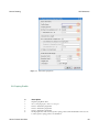
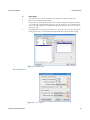
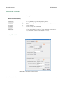
VisualTCAD provide total 4 kinds of doping profiles recently, including Uniform
Doping Profile, Gaussian Doping Profile, Erf Doping Profile and Dataset Doping
Profile etc.
Figure 3.5 Doping Profile Type.
Uniform
Doping Profile
#
Description
1
2
3
4
Inputs Doping Profile name
Chooses Doping Species: Donor or Acceptor
Inputs Concentration of the Uniform Doping Profile
Uniform Doping Profile, in the bound region the doping profile is uniform distribution and out
of the bound region has none doping distribution
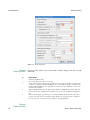
Gaussian
Doping Profile
Genius Device Simulator
67
GUI Reference
Device Drawing
#
Description
1
2
3
4
Inputs Doping Profile name
Chooses Doping Species: Donor or Acceptor
Inputs Concentration of Doping Profile, two styles to choose: concentration peak or Total Dose.
Characteristic Length, two styles to choose: Y Characteristic Length or Doping Concentration
at depth, the Distance to doping Box parameter is a relative depth to the edge of bound rectangle. The doping setting has 4 groups total, but the combination of Total Dose and Doping
Concentration is invalid.
5
6
Sets XY Ratio, the value is equal to X.char/Y.char
Gaussian Doping Profile, in the bound region the doping profile is uniform distribution and out
of the bound region the doping profile is gaussian distribution
Figure 3.6 Uniform Doping Profile.
68
Genius Device Simulator
Device Drawing
GUI Reference
Figure 3.7 Gaussian Doping Profile.
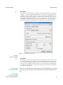
Erf Doping Profile
#
Description
1
2
3
4
5
6
Inputs Doping Profile name
Chooses Doping Species: Donor or Acceptor
Refers to Gaussian doping Profile
Refers to Gaussian doping Profile
Refers to Gaussian doping Profile
Erf Doping Profile, in the bound region the doping profile is uniform distribution and out of the
bound region the doping profile is erf distribution
Genius Device Simulator
69
GUI Reference
Device Drawing
Figure 3.8 Erf Doping Profile.
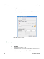
Dataset
Doping Profile
Chooses profile dataset style, total 3 kinds of dataset doping: only 1D, only 2D
and Both.
#
Description
1
2
3
Inputs Doping Profile name
Chooses Doping Species, Donor or Acceptor
About only 1D option, importing the one-dimension doping data, it incuding 2 columns, first
column is coordinate and its unit is $\nMeter$, the second column is doping concentration and
its unit is $\ICubic\cMeter$. the doping data can come from the opened data file or look for the
data file by the data path.
4
5
When VisualTCAD introduces the data from the data file, VisualTCAD needs interpolation the
mesh point data, the default linear interpolation, here provides the logarithmic interpolation,
also.
In the bound rectangle region introduces one-dimension dataset file, the baseline from point1 to
point2 is the begin of the one-dimention doping data,the end of doping profile is expanded to
the edge of the box, out of the bound region has none doping distribution.
Dataset
Doping Profile
70
Genius Device Simulator
Device Drawing
GUI Reference
#
Description
1
About only 2D option, importing the two-dimension doping data, it incuding 3 columns, first
column is x-coordinate and its unit is $\nMeter$, the second column is y-coordinate and its unit
is $\nMeter$, the third column is doping concentration and its unit is $\ICubic\cMeter$. the
value of the rectangle has been changed to 0, it means only the baseline from point 1 to point
2 is significative, VisualTCAD makes the center of the baseline as the 2D doping origin, the
doping data file introduces the two-dimension doping profile from the center of the baseline to
the doping coordinate of the doping file, the x-coordinate positive direction is left direction.
Figure 3.9 1D Dataset Doping Profile.
Dataset
Doping Profile
#
Description
1
About Both option, in the bound rectangle region the doping profile is as the same as only 1D
option and the doping data from 1D data, out of the bound rectangle region the doping profile is
as the only 2D option doping profile and the origin is the the box baseline point2, and the left 2D
doping of the box is symmetric with the right of the box. in the bound region is significant only
for one-dimension doping data, out of the bound rectangle, the point 1 and point 2 is significant
for two-dimension doping data.
Place mole
Fraction Profile
If the device includes the polycompound material, VisualTCAD introduces 2 methods to place the mole fraction of the compound, linear fraction and gaussian fraction.
Linear mole
Fraction Profile
Genius Device Simulator
71
GUI Reference
Device Drawing
#
Description
1
2
3
Inputs the linear mole fraction profile name
Inputs the range of mole fraction profile
The linear mole fraction profile is introduced to the bound rectangle region from the baseline to
the end of the bound rectangle
Figure 3.10 2D Dataset Doping Profile.
Gaussian mole
Fraction Profile
#
Description
1
2
Inputs the gaussian mole fraction profile name
Inputs the parameter of the gaussian mole fraction, including the peak, characteristic length and
ratio.
3
72
Gaussian mole fraction Profile, in the bound region the doping profile is uniform mole fraction
and out of the bound region the mole fraction profile is gaussian distribution.
Genius Device Simulator
Device Drawing
GUI Reference
Figure 3.12 Linear Mole Fraction Profile.
Genius Device Simulator
73
GUI Reference
Device Drawing
Figure 3.13 Gaussian Mole Fraction Profile.
74
Genius Device Simulator
Device Drawing
GUI Reference
Figure 3.11 Both 1D&2D Dataset Doping Profile.
Do mesh
Figure 3.14 do mesh.
#
Description
1
The minimum angle constraint of the triangle mesh is from 15 to 32 degree, the triangle angle
is wider the mesh quality is better, but at the same time the rate of generating mesh is become
slow
Genius Device Simulator
75
GUI Reference
Device Drawing
#
Description
Refine
Figure 3.15 refine.
#
Description
1
Calculates the doping Gradient and Specifies the refinement is based on the specified quantity
logarithm.
2
Refinement the mesh in doping Gradient greater than or equal to an order of magnitude, here
the range of doping Gradient is from 1 to 5.
Mesh Statistics
Figure 3.16 mesh statistics
76
Genius Device Simulator
Device Drawing
GUI Reference
#
Description
1
2
Statsitics the mesh point number, triangle number, mesh size and mesh quality etc.
Statistics the disposition of the triangle angle
Mesh 3D view
Figure 3.17 Mesh 3D view.
#
Description
1
User can rotate the structure in the windows and view in any visual angle
Save mesh file to
Figure 3.18 Save Mesh File To.
Genius Device Simulator
77
GUI Reference
Device Drawing
#
Description
1
2
Chooses the file's saving path
Inputs the file name and save the mesh structure file
Run python
Figure 3.19 run python.
#
Description
1
2
Chooses the exist python file's path
Selects the python file and open it
Export python
Figure 3.20 Export python.
78
Genius Device Simulator
Device Drawing
GUI Reference
#
Description
1
2
Chooses the file's saving path
Inputs the file's name and saves the python deck file
Genius Device Simulator
79
GUI Reference
Device Drawing
Device View
Menu
Icon
Description
Device View
Fit to View
Center Origin Point
Zoom In
Zoom Out
Ruler
80
Center the device drawing, and scale it to fit the screen size.
Center the screen at the origin of the device coordinates.
Zoom in, with the point under the mouse cursor fixed in view.
Zoom out, with the point under the mouse cursor fixed in view.
Add a ruler item for measure the linear distance between two points.
Genius Device Simulator
Device Simulation
GUI Reference
Device Simulation
Simulation Setting
Menu
Icon
Description
simulation setting
Open a structure file.
Turn on the resistive metal model (new in 1.7.1).
Running the device simulation.
Save the device simulation configuration to a directory, which will contain the
command file (.inp) and mesh file (.cgns) and data files (if needed).
Load
Resistive Metal
Run
Write Deck File
Solve
Time parameters in Transient simulation.
DC sweep parameters in DC Steady-state simulation.
Boundary and Contact settings of the device.
Physical Model and Material Model parameters.
Numerical solver paramters, including Number of Processors in parallel simulation.
Time Control
Sweep Control
Boundary Condition
Physical Model
Solver Options
Output
Open the IV data file.
Open the .vtu file to visualize the internal variables (potential and carrier concentrations, etc.) in the device.
Show IV Data
Show Visualization
Load
#
Description
1
2
Chooses the exist structure file's path
Selects the structure file and open it
Genius Device Simulator
81
GUI Reference
Device Simulation
Figure 3.21 load structure file.
Resistive Metal
When the device exist the boundary of the metal, user should be set it to "Soder
pad" Boundary and open the "Resistive Metal" button before load the device structure in the "Device Simulation" window.
Figure 3.22 define boundary.
82
Genius Device Simulator
Device Simulation
GUI Reference
#
Description
1
2
Choose boundary tool
Add boundary label(Anode and Cathode)
Figure 3.23 change boundary setting.
#
Description
1
2
3
In "Device Simulation" window, load the mesh, and click "Boundary Settings"
Click "More>>" to see the full list
Change from "Neumann" to "Ohmic" and "Solder pad" boundary conditions, respectively.
Run simulation
Figure 3.24 run simulation.
#
Description
1
When user runs the simulation, VisualTCAD will remind user to save the simulation settings
before running it
write deck file
Genius Device Simulator
83
GUI Reference
Device Simulation
#
Description
1
User can transform the simulation to genius deck file and run the deck file in Genius to finish
the simulation.
Figure 3.25 write deck file.
Time Control
Figure 3.26 time control.
#
Description
1
For transient simulation, the time control setting needs set start time, step time, stop time and
Maxmum step time etc.
2
Other options, user can choose to set maxmum voltage step
Boundary condition
84
Genius Device Simulator
Device Simulation
GUI Reference
#
Description
1
2
3
4
Clicks to choose the boundary
Chooses the contact type, total includes many types, here chooses the ohmic contact
Sets ohmic contact parameters, some contact have no parameters, such as Neumann boundary.
Sets boundary z width, the priority is higer than global z width setting.
Figure 3.27 Boundary condition.
physical model
Figure 3.28 Global model.
Genius Device Simulator
85
GUI Reference
Device Simulation
#
Description
1
2
Sets global parameter, temperature and z width parameters
Chooses the physical equations, including Basic Drift-diffusion equations, Drift-diffusion equations with lattice heating and Energy-balanced drift-diffusion equations. Here chooses Basic
Drift-diffusion equations
Figure 3.29 physical model.
#
Description
1
2
Sets physical model of silicon material and other materials choosing the default model
Carrier statistics, chooses Boltzmann distribution or Fermi-Dirac distribution. Energy balance
equaption, When the Energy-Balance equation solver is selected in the METHOD command, this
parameter selectively enables the equations for lattice temperature, electron temperature and
hole temperature.
3
4
5
86
Transverse E-Field, Use effective surface electric field for carrier mobility calculation at insulator-semiconductor interface. Longitudinal, Synonym to Mobility.Force. When H.Mob is
enabled, this parameter selects the driving field used in high-field mobility calculation.
When ImpactIonization is enabled, this parameter selects the driving field used in impact
ionization coefficient calculation. including Qf Gradient, E dot J, E along mesh-edge and simple
E field.
Activates the Band-to-Band Tunneling (BBT) generation, and selects whether the BBT generation should be calculated with the local model or the non-local model. Only the local model is
currently implemented. Whether the Carrier trapping is enables
Genius Device Simulator
Device Simulation
GUI Reference
#
Description
1
2
3
Sets material model of silicon material and other materials choosing the default model
Basic model, including Default model only
Basic model, user can modify the parameter of the model by clicking the right button Add Property and input the paramenter Name and Value. User can inputs print as the parameter Name
and 1 as the Value, then runs the simulation, all parameters setting of the selected model are
printed in Log file.
4
Other Material model, using the same method, user can modify other model by modifying the
model parameters, the model including Band, Impact, Mobility, Optical, Thermal and Trap.
Figure 3.30 material model.
Solver Options
Figure 3.31 Solver options.
Genius Device Simulator
87
GUI Reference
Device Simulation
#
Description
1
2
3
4
Chooses the number of processor of simulation
Chooses the maxmum iterations, the default setting is 30
Chooses whether using update damping and sets potential damping factor
Selects the element truncation strategy used in simulation, including Always truncate, Never
truncate and truncate at boundary.
5
88
Selects the linear solver algorithm, including Direct(MUMPS), Direct(SuperLU), iterative(BCGS+ASM)
and iterative(BCGS+ILU).
Genius Device Simulator
Circuit Schematics
GUI Reference
Circuit Schematics
Place Circuit Component
Menu
Icon
Description
device setting
Add a Spice component (compact model) to the circuit.
Add a numerical device to the circuit, for mix-mode simulation.
Component
Numerical Device
Common Circuit Components
GND.
Add a resistor component.
Add a capacitor component.
Add an inductor component.
Ground
Resistor
Capacitance
Inductance
Probe
Add a voltage probe to the circuit, for monitoring voltage difference between
two circuit nodes.
Voltage Probe
Add a current probe to the circuit, for monitoring current through a circuit
branch.
Current Probe
Connection
Add wirings to the circuit.
Wire
Component
#
Description
1
2
3
According to user need to select component
Simple description of the component
Component preview window
Genius Device Simulator
89
GUI Reference
Circuit Schematics
Figure 3.32 Component.
Numerical Device
Figure 3.33 Numerical Device.
90
#
Description
1
2
Load the device component file's path
Selects the device component file and opens it
Genius Device Simulator
Circuit Schematics
GUI Reference
Simulation Control
Menu
Icon
Description
Circuit simulation setting
Simulation Setup
Solver Options
Run Simulation
Check Netlist
View Netlist
Write Deck Files
Choosing the analysis type and setting analysis parameters.
Numerical solver paramters, including Number of Processors in parallel simulation.
Start the simulation.
Check the validity of the circuit netlist.
Viewing the netlist file (in SPICE format).
Save the circuit simulation to a direcotry, which contains the circuit netlist, Genius command file, mesh file and other data files (if needed).
Setup Simulation
Figure 3.34 Setup simulation transient analysis.
Genius Device Simulator
91
GUI Reference
Circuit Schematics
#
Description
1
2
3
Selects the analysis type, Here choosing transient simulation type
Sets the transient simulation condition
Initial operator point analysis options, including the number of ramp-up steps of the bigest
nonzero External Source by Attach statement, the maxmum voltage steps, initial value of Gmin
stepping and target of Gmin stepping. The perpose of the initial setting is making the simulation
more convergence.
Figure 3.35 Setup simulation DC sweep analysis.
92
#
Description
1
2
3
Selects the analysis type, here choosing DC Sweep simulation type
Selects the sweep variable
Selects the sweep component and sets the sweep range
#
Description
1
2
Selects the analysis type, here choosing AC Sweep simulation type
Selects the AC sweep step spacing linear or logarithmic and sets the sweep range
Genius Device Simulator
Circuit Schematics
GUI Reference
#
Description
1
2
Selects the analysis type, here choosing Operation Point simulation type
Here no settings are needed
Figure 3.36 Setup simulation AC sweep analysis.
Check netlist
#
Description
1
When user finishes the circuit schematic, user need check the netlist, when it is OK, user can
run the circuit simulation.
Genius Device Simulator
93
GUI Reference
Circuit Schematics
Figure 3.38 check netlist.
Figure 3.37 Setup simulation operation point analysis.
View netlist
94
#
Description
1
According to the circuit schematic, VisualTCAD generates the netlist automatically,the netlist
file includes circuit components and wire connection etc.
Genius Device Simulator
Circuit Schematics
GUI Reference
Figure 3.39 View netlist.
Genius Device Simulator
95
GUI Reference
Circuit Schematics
Result Analysis
Menu
Icon
Description
Simulation Results
Load Spice Raw File
Plot Probe Wave
96
Open the simulated waveform in a spreadsheet window.
Plot the waveform of voltage and current probes.
Genius Device Simulator
Circuit Schematics
GUI Reference
Schematics View
Menu
Icon
Description
Schematics View
Fit to View
Center Origin Point
Zoom In
Zoom Out
Genius Device Simulator
Move the schematics to center and scale it to the fit the screen size.
Move the schematics to center.
Zoom in.
Zoom out.
97
GUI Reference
Device Visualization
Device Visualization
View
Menu
Icon
Description
General Options
Switch Background Color
Inverse Y of View Point
Toggle the screen background color between black and white.
Toggle the direction of the y-axis between up and down.
Camera Options
Reset View
View at +X
View at -X
View at +Y
View at -Y
View at +Z
View at -Z
98
Reset camera position, orientation and focal parameters.
View the device from the direction of +x axis.
View the device from the direction of -x axis.
View the device from the direction of +y axis.
View the device from the direction of -y axis.
View the device from the direction of +z axis.
View the device from the direction of -z axis.
Genius Device Simulator
Device Visualization
GUI Reference
Draw
Menu
Icon
Description
Device Drawing
Draw Device Region
Draw Device Material
Draw Device Boundary
Draw Mesh
Plot the regions in the device structure.
Plot the materials in the device structure.
Plot the boundary and interfaces in the device structure.
Plot the mesh elements in the device structure.
Device Variable Plotting
Draw Pseudo Color
Draw Contour
Draw Vector
Genius Device Simulator
Draw a pseudo color plot of the selected variable.
Draw a contour line (surface) plot of the selected variable.
Draw a vector plot of the selected variable.
99
GUI Reference
Device Visualization
Animating the simulation result
Menu
Icon
Description
Animation Control
First Frame
Previous Frame
Next Frame
Last Frame
Play/Pause
Show the first frame of the simulation results.
Show the previous frame.
Show the next frame.
Show the last frame.
Play (or Pause) the animation.
Add Frames
Add Frame(s)
100
Add frames (.vtu files) to the animation.
Genius Device Simulator
Spreadsheet
GUI Reference
Spreadsheet
Menu
Icon
Description
Spreedsheet Operation
Insert one row in the spreadsheet.
Insert one column in the spreadsheet.
Delete the selected rows in the spreadsheet.
Delete the selected columns in the spreadsheet.
Plot the data in selected columns.
Use mathematical calculator to calculate data entries in the selected column.
Insert Row
Insert Column
Delete Row
Delete column
Plot Column
Calculator
Scripting
Run a spreadsheet Python script.
Run Python Script
Plot column
Figure 3.40 plot column.
#
Description
1
2
User need select at least two columns and set one column data as x-axis data column
Calculator
#
Description
1
2
3
VisualTCAD offers calculate function, user can obtain the expression
The calculate data come from the column data.
The expression can include the function of VisualTCAD offers, including absolute value calculate and square calculate etc.
Genius Device Simulator
101
GUI Reference
Spreadsheet
Figure 3.41 Calculator.
102
Genius Device Simulator
XY Plotting
GUI Reference
XY Plotting
Menu
Icon
Description
Plot Data Source
Insert Curve
Insert Group
Delete
Insert curve in the current group.
Insert group in the plot.
Delete the selected curve or group.
Edit Plot Properties
Edit Axis Properties
Edit Curve Properties
Palette Manager
Edit the axis properties, e.g. the axis scale, range and tick marks.
Edit the curve properties, eg. the line style, symbol style and color.
Edit the plot curve style palletes.
Input/Output
Run Python Script
Export Python Script
Run a Python for curve plotting..
Export the current plot to a python script file.
Insert Curve
Figure 3.42 insert curve.
Genius Device Simulator
103
GUI Reference
XY Plotting
#
Description
1
User can insert several curve to one plot, the x- and y-variable come from the open any data file.
the left window is for choosing the x-variable and only can choose one column data.
2
The right window is for choosing y-variables, user can choose several column data as y variables
at the same time.
Edit Axis Properties
Figure 3.43 Edit Axis Properties.
#
Description
1
2
3
User can edit the plot axis properties, inputs the left y-axis title
Selects the Axis Scale type, linear scale, logarithmic scale etc.
Inputs the range of value of the axis.
Edit Curve
properties
Figure 3.44 Edit Curve Properties.
104
Genius Device Simulator
XY Plotting
GUI Reference
#
Description
1
2
User can edit each curve properties and slect each line axis style
Selects each curve line and symbol style
Palette Manageer
Figure 3.45 Palette Manager.
#
Description
1
2
3
VisualTCAD offers 7 palettes for user
User can edit new palette
User can edit new curves of the selected palette and restore default palettes
Genius Device Simulator
105
GUI Reference
Text Editor
Text Editor
Search
Menu
Icon
Description
Search a string in the text.
Go to the next match in the text.
Go to the previous match in the text.
Replace the matched string.
Find
Find Next
Find Previous
Replace
Find
Figure 3.46 Find.
#
Description
1
2
Inputs the find text
Selects the properties
Replace
Figure 3.47 Replace.
106
Genius Device Simulator
Text Editor
GUI Reference
#
Description
1
2
2
Inputs the find text
Inputs the replace text
Selects the properties
Genius Device Simulator
107
GUI Reference
Text Editor
Options
Menu
Icon
Description
Spreedsheet
Highlight the text with the selected syntax mode, eg.Genius,Spice,Python,XML
or no-highlight.
Syntax HighLight Mode
Font settings of the text window.
Font Settings
Font Settings
Figure 3.48 Font Settings.
108
#
Description
1
2
3
4
Selects the font
Selects the font style
Selects the font size
Other effects
Genius Device Simulator
Text Editor
GUI Reference
Tools
Menu
Icon
Description
Simulation Tools
Run As Genius Deck
Run As SPICE Deck
Run As Python Script
Genius Device Simulator
Run Genius device simulator with the curent file as the command input.
Run SPICE circuit simulator with the current file as the circuit deck.
Run the text file as a Python Script.
109
GUI Reference
110
Text Editor
Genius Device Simulator
CHAPTER
4 Programming Reference
Device2D Drawing
Class Device2DScript
The Device2DScript exposes APIs for device2d drawing in python language.
Method scriptType
scriptType()
Returns
Object name "device2dscript".
Method addPolyLineItem
addPolyLineItem(points)
Arguments
points list, a list of points which to build a poly line. For example, points =
(-400,0), (400,0), (400,1000), (-400, 1000), addPolyLineItem(points) will draw
line((-400,0), (400,0)), line((400,0), (400,100)), line((400, 1000), (-400,1000)).
Method addRegionLabelItem
addRegionLabelItem(label,materail, pos, areaConstrain=0.01,
strColor="#ffb6c1")
Arguments
label string, name of the region label item.
material string, name of material which used in region.
pos point, region item position.
areaConstrain double, set region mesh area constrain.
Genius Device Simulator
111
Programming Reference
Device2D Drawing
strColor string, name of color which used in region.
Method addRegionDoping
addRegionDoping(label,property, concentration)
Arguments
label string, name of the region.
property string, property of region,"Nd" or "Na".
concentration double, concentration of region.
Method addRegionMoleFraction
addRegionMoleFraction(label, x, y=-1.0)
Arguments
label string, name of the region.
x double, x fraction.
y double, y fraction.
Method addDataset
addDataset(xList, yList, vList, dsName="")
Arguments
xList list, list of x coordinate position.
yList list, list of y coordinate position.
vList list, list of value.
dsName string, name of dataset.
Returns
dataset label for this dataset, which append SHA1 to dsName.
Method addDataset
addDataset(type, filename)
Arguments
112
type string, 1D or 2D dataset file.
Genius Device Simulator
Device2D Drawing
Programming Reference
filename string, dataset file name.
Returns
dataset label for this dataset, which append SHA1 to filename.
Method addDopingProfileItem
addDopingProfileItem(attr)
Arguments
attr list, a list of name and value pair for profile item.
Method addMoleFractionItem
addMoleFractionItem(attr)
Arguments
attr list, a list of name and value pair for mole fraction item.
Method addBoundaryItem
addBoundaryItem(label, segment, strColor="#ff0000")
Arguments
label string, label for boundary item.
segment list, point p1 and p2 to decide item region.
strColor string, background color for item.
Method addMeshSizeCtrlItem
addMeshSizeCtrlItem(division, points)
Arguments
division int, number of division.
points list, start point and end point to decide MeshSizeCtrlItem.
Method addRulerItem
addRulerItem(points)
Genius Device Simulator
113
Programming Reference
Arguments
Device2D Drawing
points list, start point and end point to decide RulerItem.
Method addPointItem
addPointItem(point)
Arguments
point list, (x, y) to decide PointItem.
Method doMesh
doMesh( optimization = 1, meshCmd = "pzADenQq30", max_d=3.0,
signed_log=true)
Arguments
optimization int, times to refine mesh.
meshCmd string, command to do mesh.
max_d double.
signed_log bool.
Method exportMesh
exportMesh( filename)
Arguments
filename string, name of tif file when export mesh.
Method clear
clear()
Method saveToFile
saveToFile(filename)
Arguments
filename string, filename to save file, which can be relative or absolute filename,
if relateive, save in current directory where program is running.
Method setTitle
setTitle( title)
114
Genius Device Simulator
Device2D Drawing
Arguments
Genius Device Simulator
Programming Reference
title string, title for Device2D SubWindow.
115
Programming Reference
Curve Plot
Curve Plot
PlotScript
The PlotScript exposes APIs for curve ploting in python language.
Method scriptType
scriptType( )
Returns
Return the object name "plotscript".
Method curveGroupCount
curveGroupCount( )
Returns
Return the count of curve groups.
Method curveCountAt
curveCountAt( group)
Arguments
Returns
group int, group index.
Return curve count at group group
Method insertCurveGroup
insertCurveGroup( pos, groupTitle="Group", groupPalette = QString())
Arguments
pos int, index of curve group.
groupTitle string, title for this curve group.
groupPalette string, palette name for this curve group.
Method removeCurveGroup
removeCurveGroup( int pos)
116
Genius Device Simulator
Curve Plot
Programming Reference
Arguments
pos int, index of curve group which will be deleted .
Method setGroupTitle
setGroupTitle( group, title)
Arguments
group int, index of curve group.
title string, title for curve group.
Method insertCurve
insertCurve( group, pos, xData, yData, title = "curve", properties
= QVariant())
Arguments
group int, index of curve group.
pos int, index of curve in curve group.
xData list, data for x coordinate .
yData list, data for y coordinate.
title string, title for the curve.
properties list, a list of curve properties.
Method clear
clear()
Method saveToFile
saveToFile( filename)
Arguments
filename string, save to file with filename.
Method setTitle
setTitle( title)
Arguments
Genius Device Simulator
title string, title for plot subwindow.
117
Programming Reference
SpreadSheet
SpreadSheet
class SpreadSheetScript
The SpreadSheetScript class exposes APIs for spreadsheet operations in python
language.
Method scriptType
scriptType()
Returns
Return the object name "ssheetscript".
Method getColumnName
getColumnName( column)
Arguments
Returns
column int, index of column, index from 0.
Return the name of column.
Method getColumnData
getColumnData( column)
Arguments
Returns
column int, index of column, index from 0.
Return data in column.
Method insertRows
\GSyntax{insertRows}( row, count)
Arguments
row int, row index where rows will be inserted.
count int, number of rows will be inserted.
Method insertColums
insertColums( column, count)
118
Genius Device Simulator
SpreadSheet
Arguments
Programming Reference
column int, column index where columns will be inserted.
count int, number of columns will be inserted.
Method setColumnData
setColumnData( column, data)
Arguments
column int, index of column.
data list, assign data to column.
Method setColumnName
setColumnName( column, name)
Arguments
column int, index of column.
name string, name for column.
Method calcColumn
calcColumn( column, expression)
Arguments
column int, index of column.
expression string, expression to compute data for column.
Method saveToFile
saveToFile( filename)
Arguments
filename string, save to file with filename.
Method setTitle
setTitle( title)
Genius Device Simulator
119
Programming Reference
Arguments
SpreadSheet
setTitle string, title for spreadsheet subwindow.
Method clear
clear()
120
Genius Device Simulator
MainWindow
Programming Reference
MainWindow
Class MainWindowScript
The MainWindowScript class exposes APIs for operations in top level in python
language.
Method scriptType
scriptType()
Returns
Return the object name "mainwindowscript".
Method openDocumentFromFile
openDocumentFromFile( filename)
Arguments
filename string, name of file which to open.
Method saveAllToFile
saveAllToFile( filepath)
Arguments
filepath string, path to save content of all subwindow to file .
Method newWindow
newWindow( type, title)
Arguments
type string, type of window, type can be "Device2D" "Plot" or "SpreadSheet".
title string, title for window.
Returns
Return a pointer which point to created window, if failed, return
NULL.
Method getWindowByName
getWindowByName( subWindowName)
Genius Device Simulator
121
Programming Reference
Arguments
Returns
MainWindow
subWindowName string, name of subWindow.
If find a subwindow which has name \GSyntax {subWindowName},
return a pointer which point to it, else return NULL.
Method getWindowByNumber
getWindowByNumber( number)
Arguments
Returns
122
number int, index of subwindow.
If find a subwindow which has index \GSyntax {\GSyntax {number}},
return a pointer which point to it, else return NULL.
Genius Device Simulator