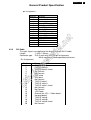
1
Chassis: HUDSON 9 24 inch TFT WXGA LCD Colour Monitor el. ne t 240BW 9CS /00 240BW 9CB /00 240BW 9CB /27 240BW 9CB /69 240BW 9CB /75 240BW 9CB /93 Horizontal frequencies 30 - 8 3 kHz TABLE OF CONTENTS Description Page Wiring Diagram--------------------------------------------30 Block Diagram----------------------------------------------31 tp :// ww w. wj Description Page Important Safety Notice-------------------------------------2 Technical Data------------------------------------------------ 3 Installation------------------------------------------------------4 T roubleshooting-----------------------------------------------5 On Screen Display-----------------------------------------6~7 Lock/unlock, Aging,Factory mode-------------------------8 Philips Pixel Defect Policy ---------------------------------9 Mechanical Instructions -----------------------------10~11 Color adjustment -------------------------------------------12 F AQs (Frequently Asked Questions)--------------13~14 Electrical instruction ---------------------------------15~16 DDC Instructions & Serial Number ----------------17~23 DDC DATA ----------------------------------------------24~27 Firmware Upgrade for CPU- ----------------------------28 Failure Mode Of Panel - ----------------------------------29 SAFETY Scaler Diagram & C.B.A. ----------------------------32~40 Power Diagram & C.B.A. ---------------------------41~46 Control Diagram & C.B.A. ---------------------------47~48 LED Diagram & C.B.A. ---------------------------49~50 USD Diagram & C.B.A. ---------------------------51~53 Inverter Diagram & C.B.A. ---------------------------54~56 General product specification----------------------57~84 Exploded V iew ---------------------------------------------85 Spare/ Recommended P arts List------------------------86 PCBA photos--------------------------------------------------87 Repair tips-----------------------------------------------88~89 Repair Flow chart--------------------------------------90~92 Safety Test Requirments---------------------------------93 NOTICE ht ANY PERSON ATTEMPTING TO SERVICE THIS CHASSIS MUST FAMILIARIZE HIMSELF WITH THE CHASSIS AND BE AWARE OF THE NECESSARY SAFETY PRECAUTIONS TO BE USED WHEN SERVICING ELECTRONIC EQUIPMENT CONTAINING HIGH VOL TAGES. CAUTION: USE A SEPARATE ISOLATION TRANSFORMER FOR THIS UNIT WHEN SERVICING. REFER TO BACK COVER FOR IMPORTANT SAFETY GUIDELINES Published by Philips Consumer Lifestyle Copyright reserved Subject to modification Aug 25 2008 GB 312278518210 Important Safety Notice LCD 2 2 240BW9 8 LCD 220BW Proper s ervic e and repair is important to the safe, reliable FOR PRODUCTS CONTAINING LASER : operation of all Philips Consumer Electronics Company DANGER - equipment. The service procedures recommended by Philips and described in this service manual a re eff ective methods of Invisible laser radiation when open. AVOID DIRECT EXPOSURE TO BEAM. performing service operations . Some of these service CAUTION - operations require the us e of tools speciall y desi gned for the Use of controls or adjustments or performance of procedures other than purpose. The special tools should be used when and as those specified herein may result in recomm ended. hazardous radiation exposure. It is im portant to note that this m anual c ontains various CAUTION - CAUTI ONS and NOTICES which should becarefully read in The use of optical instruments with this product will increase eye hazard. order to m inimize the risk of personal injury to service personnel . The possibility exists that improper service t methods may damage the equipment. It is also important to ne underst and that these CAUTIONS and NOTICES ARE NOT EXHAU STIVE. Philips could not possibly know, evaluate and TO ENSURE THE CONTINUED RELIABILITY OF THIS advise the servic etrade of all conceivable ways i n which PRODUCT , USE ONLY ORIGINAL MANUFACTURER'S consequences of each way. Consequently, Philips has not REPLACEMENT PAR TS, WHICH ARE LISTED WITH THEIR PART undertaken any such broad evaluation. Accordingly, NUMBERS IN THE PARTS LIST SECTION OF THIS who uses a servi ce procedure or tool which is not SERVICE MANUAL. neither his safety nor the safe operation of the equipment will be jeopardized by the service method selected. * * Hereafter throughout this manual, Philips Consumer Electronics Company will be referred to as Philips . * * w. wj recommended by Philips must first satisfy himself thoroughly that el. service might be done or of the possible hazardous ww Take care during handling the LCD module with backlight unit - Must mount the module using mounting holes arranged in four WARNING :// corners. Critical components having special safety characteristics are enclosed within a broken line tp identified with a by the Ref. No. in the parts list and - Do not press on the panel, edge of the frame strongly or electric shock as this will result in damage to the screen. - Do not scratch or press on the panel with any sharp objects, such as pencil or pen as this may result in damage to the panel. (where several critical components are grouped in one area) exploded views. ht along with the safety symbol on the schematics or - Protect the module from the ESD as it may damage the electronic circuit (C -MOS). Use of substitute replacement parts which do not have the - Make certain that treatment body are grounded through same speci fied safety characteristic s may create shock, fire, wrist band. or other hazards . - Do not leave the module in high temperature and in areas of high Under no circumstances should the original design be humidity for a long time. modified or altered without written permission from Philips. Philips assumes no liability, express or implied, arising out of - Avoid contact with water as it may as hort circuit within the module. - If the surface of panel become dirty, please wipe it off with a soft any unauthorized modification of design. Servicer assumes all liability. material. (Cleaning with a dirty or rough cloth may damage the panel.) 240BW9 LCD 3 Technical Data SEC Panel Type NR. : SEC LTM240CT03 Resolution : 1920x1200 (WUXGA) Outside dimensions : 546.4 (H) x 352 (V) x 36.3 (D) Pitch ( mm ) : 0.27 Color pixel arrangement : RGB vertical stripes Display surface : Haze 25% , Hard-coating(3H) Color depth : 16.7 M colors Backlight : U-type 6 CCFTs Active area(WxH) : 518.4(H) x 324(V) View angle (CR>10) : 160/160 (typ) for H/V Contrast ratio : 1000:1 (typ) White luminance : 400 (typ) Color gamut : 92% Gate IC : LDI Source IC : LDI Response time : 5 ms(typ) Pin No. 2 T.M.D.S. data2+ 3 T.M.D.S. data2 shield 4 No Connect 5 No Connect 6 DDC clock 7 DDC data 8 No Connect 9 T.M.D.S. data1- 10 T.M.D.S. data1+ 11 T.M.D.S. data1 shield 12 No Connect 13 No Connect t Hor. : 24 – 94 K Hz Ver.: 48 - 85 Hz Video dot rate: 210MHz for VGA and 170 for DVI Power input: 90-264 V AC, 50/60 ± 2 Hz Power consumption: < 85 W / after 30 mins, meet EPA tier 2 requirement T.M.D.S. data2- ne Scanning frequencies Description 1 +5V Power (1)D-SUB analog R/G/B separate inputs, H/V sync separated, Composite 15 Ground (for +5V) – Cable detect (H+V) TTL level, SOG sync 16 (2) DVI digital Panel Link TMDS inputs 17 Power input connection Power cord length Power cord type : 1.8 M : 3 leads power cord with protective earth plug. Power management VSYNC Video Pwr-cons. Power-On On On active 85W typical Off Off Off Indication Rec. time Blue LED -- :// HSYNC ww The monitor must comply with the Microsoft On Now specification, and meet EPA requirements. Mode (After 30 mins) Blue LED Blinking 3 sec on, 3sec off <1W LED Off tp N/A <1W (<110V & no audio) <2W (<220V & no audio) ht DC Power Off blanked PIN SIGNAL No. PIN 18 19 T.M.D.S. data0 shield 20 No Connect Hot plug detect T.M.D.S. data0- T.M.D.S. data0+ w. wj 0 °C - 40°C Ambient temperature: el. 14 Functions: SIGNAL No. 1 Red 9 DDC +3.3V or +5V 2 Green/ SOG 10 Logic GND 3 Blue 11 Sense (GND) 4 Sense (GND) 12 Bi-directional data 5 Cable Detect (GND) 13 H/H+V sync 6 Red GND 14 V-sync 7 Green GND 15 Data clock 8 Blue GND <3s 21 No Connect 22 T.M.D.S clock shield 23 T.M.D.S. clock+ 24 T.M.D.S. clock- Susceptibility of display to external environment Operating - Temperature : 0 to 40 degree C - Humidity : 80% max - Altitude : 0-3658m - Air pressure : 600-1100 mBAR Storage - Temperature - Humidity - Altitude - Air pressure : -20 to 60 degree C : 95% max : 0-12192m : 300-1100 mBAR Note: recommend at 5 to 35°C, Humidity less than 60 % 4 240BW9 LCD Installation Accessory Pack Unpack all the parts. Front View Product Description Power cord DVI cable (Optional) VGA cable EDFU pack To switch monitor's power On and Off 2 To access OSD menu 3 To adjust the OSD menu Connecting to Your PC 4 To adjust brightness of the display 1) Connect the power cord to the back of the monitor firmly. (Philips has pre-connected VGA cable for the first installation. 5 To adjust volume of the display 6 Automatically adjust the horizontal position, vertical position, phase and clock settings / Return to previous OSD level 7 SmartImage. There are five modes to be selected: Office Work, Image Viewing, Entertainment, Economy, and Off 8 Earphone jack ne t 1 ww w. wj el. Audio cable ht tp :// Rear Viewʳ 2) Connect to PC 1ʳ USB upstream port and downstream portʳ 2ʳ VGA inputʳ 3ʳ DVI-D input (available for selective models)ʳ 4ʳ PC Audio input ʳ 5ʳ AC power inputʳ 6ʳ Kensington anti-thief lockʳ (a)ʳ Turn off your computer and unplug its power cable.ʳ (b)ʳ Connect the monitor signal cable to the video connector on the back of your computer.ʳ (c)ʳ Connect the PC audio cableʳto the audio connector on the back of your computer.ʳ (d)ʳ Connect the USB upstream port on the monitor and the USB port on PC with a USB cable. The USB downstream port is now ready for any USB device to plug in.ʳ (e)ʳ Plug the power cord of your computer and your monitor into a nearby outlet.ʳ (f)ʳ Turn on your computer and monitor. If the monitor displays an image, installation is complete.ʳ 240BW9 LCD Trouble shooting 5 This page deals with problems that can be corrected by a user . If the problem still persists after you have tried thesesolutions, contact Philips customer service representative. Common Problems Having this problem Check these items 1.Make sure the power cord is plugged into the power outlet and into the back of the monitor. 2.First, ensure that the power button on the front of the monitor is in the OFF position, then press it to the ON position. No Picture (Power LED is amber or yellow) 1.Make sure the computer is turned on. 2. Make sure the signal cable is properly connected to your computer. 3.Check to see if the monitor cable has bent pins. 4.The Energy Saving feature may be activated Screen says 1. Make sure the monitor cable is properly connected to your computer. (Also refer to the Quick Set-Up Guide). 2.Check to see if the monitor cable has bent pins. 3. Make sure the computer is turned on. AUT O button not working properly 1.The Auto Function is designed for use on standard Macintosh or IBM-compatible PCs running Microsoft Windows. 2. It may not work properly if using nonstandard PC or video card. el. ne t No Picture (Power LED not lit) w. wj Imaging Problems 1.Press the Auto button. 2. Adjust the image position using the Horizontal Position and/or V ertical Position in OSD Main Controls. Image vibrates on the screen Check that the signal cable is properly connected to the graphics board or PC. V ertical flicker appears 1. Press the Auto button. 2. Eliminate the vertical bars using the More Settings of Phase/Clock in OSD Main Controls. 1. Press the Auto button. 2. Eliminate the vertical bars using the More Settings of Phase/Clock in OSD Main Controls. ht tp Horizontal flicker appears :// ww Display position is incorrect The screen is too bright or too dark Adjust the contrast and brightness on OSD Main Controls. (The backlight of the LCD monitor has a fixed life span. When the screen becomes dark or begins to flicker , please contact your dealer). An after-image appears If an image remains on the screen for an extended period of time, it may be imprinted in the screen and leave an afterimage. This usually disappears after a few hours. An after-image remains after the power has been turned off. This is characteristic of liquid crystal and is not caused by a malfunction or deterioration of the liquid crystal. The after-image will disappear after a peroid of time. Green, red, blue, dark, and white dots Remains The remaining dots are normal characteristic of the liquid crystal used in today's technology. 6 240BW9 LCD On Screen Display Description of the On Screen Displayʳ What is the On-Screen Display?ʳ ww w. wj el. ne t On-Screen Display (OSD) is a feature in all Philips LCD monitors. It allows an end user to adjust screen performance or select functions of the monitors directly through an on-screen instruction window. A user friendly on screen display interface is shown as below : ʳ :// Basic and simple instruction on the control keys.ʳ ht tp In the OSD shown above users can press confirm the choice or change.ʳ buttons at the front bezel of the monitor to move the cursor, to 240BW9 LCD 7 On Screen Display The OSD Treeʳ ht tp :// ww w. wj el. ne t Below is an overall view of the structure of the On-Screen Display. You can use this as a reference when you want to work your way around the different adjustments later on.ʳ ʳ Resolution notificationʳ This monitor is designed for optimal performance at its native resolution, 1920x1200@60Hz. When the monitor is powered on at a different resolution, an alert is displayed on screen: Use 1920x1200@60Hz for best results.ʳ Display of the native resolution alert can be switched off from Setup in the OSD (On Screen Display) menu.ʳ Lock/Unlock,Aging,Factory Mode 240BW9 LCD To Lock/Unlock OSD FUNCTION(User Access Aging Mode) The OSD function can be locked by pressing"OK"button(1) for more than 10 seconds, the screen shows following windows for 4 seconds. Every time when you press"OK" button, this message appears on the screen automatically . Mode Step 1 : Access Factory Mode then enter Factory Menu. Step 2 : By pressing " UP " and " DOWN" key to Burning Icon. Press "MENU " then press " UP " and " DOWN " key to turn on Aging Mode. el. ne t Unlock OSD function Unlocked OSD function can be released by pressing "OK" button for more than 10 seconds again. Step 3 : Disconnect interface cable between Monitor and PC. After 3 seconds, bring up: w. wj Access Factory Mode tp :// ww 1). Turn off monitor. 2). [Push "AUT O" & "MENU" buttons at the same time and hold them] +[Press "power" button until comes out "Windows screen" ] => then release all buttons 3).Press "MENU" button, wait until the OSD menu with Characters "HUDSON 240SW9 V0.07 2007-12-21 " (below OSD menu) come on the Screen of the monitor. Factory Mode indicator ht 8 Factory Menu Cursor can move on gray color area Hot key function: by pressing " UP " and " DOWN " key Simultaneously at User Mode (or Factory Mode) (PS: The Of fset R G B function can be used on reduce or eliminate snowy noise on the background when the resolution of video signal is 1680*1050 vertical 60Hz. Slightly increase or decrease the value until snowy noise completely disappear . repeatly Connect Signal cable again=> go back to normal display 240BW9 LCD 9 Philips Pixel Defect Policy Philips' Flat Panel Monitors Pixel Defect Policyʳ Philips strives to deliver the highest quality products. We use some of the industry's most advanced manufacturing processes and practice stringent quality control. However, pixel or sub pixel defects on the TFT LCD panels used in flat panel monitors are sometimes unavoidable. No manufacturer can guarantee that all panels will be free from pixel defects, but Philips guarantees that any monitor with an unacceptable number of defects will be repaired or replaced under warranty. This notice explains the different types of pixel defects and defines acceptable defect levels for each type. In order to qualify for repair or replacement under warranty, the number of pixel defects on a TFT LCD panel must exceed these acceptable levels. For example, no more than 0.0004% of the sub pixels on a 19" XGA monitor may be defective. Furthermore, Philips sets even higher quality standards for certain types or combinations of pixel defects that are more noticeable than others. This policy is valid worldwide.ʳ Black Dot Defects Black dot defects appear as pixels or sub pixels that are always dark or 'off'. That is, a dark dot is a sub-pixel that stands out on the screen when the monitor displays a light pattern. These are the types of black dot defects: One dark sub pixel Two or three adjacent dark sub pixels ne t Proximity of Pixel Defects el. Because pixel and sub pixels defects of the same type that are near to one another may be more noticeable, Philips also specifies tolerances for the proximity of pixel defects. Pixel Defect Tolerances In order to qualify for repair or replacement due to pixel defects during the warranty period, a TFT LCD panel in a Philips flat panel monitor must have pixel or sub pixel defects exceeding the tolerances listed in the following tables. w. wj Pixels and Sub pixels ww A pixel, or picture element, is composed of three sub pixels in the primary colors of red, green and blue. Many pixels together form an image. When all sub pixels of a pixel are lit, the three colored sub pixels together appear as a single white pixel. When all are dark, the three colored sub pixels together appear as a single black pixel. Other combinations of lit and dark sub pixels appear as single pixels of other colors. Types of Pixel Defects :// Pixel and sub pixel defects appear on the screen in different ways. There are two categories of pixel defects and several types of sub pixel defects within each category. ht tp Bright Dot Defects Bright dot defects appear as pixels or sub pixels that are always lit or 'on'. That is, a bright dot is a sub-pixel that stands out on the screen when the monitor displays a dark pattern. There are the types of bright dot defects: BRIGHT DOT DEFECTS ACCEPTABLE LEVEL MODEL 240BW9 1 lit subpixel 3 2 adjacent lit subpixels 1 3 adjacent lit subpixels (one white pixel) 0 Distance between two bright dot defects* >15mm Total bright dot defects of all types BLACK DOT DEFECTS 3 ACCEPTABLE LEVEL MODEL 240BW9 1 dark subpixel 5 2 adjacent dark subpixels 2 3 adjacent dark subpixels 0 Distance between two black dot defects* One lit red, green or blue sub pixel Two adjacent lit sub pixels: - Red + Blue = Purple - Red + Green = Yellow - Green + Blue = Cyan (Light Blue) Three adjacent lit sub pixels (one white pixel) >15mm Total black dot defects of all types TOTAL DOT DEFECTS 5 ACCEPTABLE LEVEL MODEL A red or blue bright dot must be more than 50 percent brighter than neighboring dots while a green bright dot is 30 percent brighter than neighboring dots. Total bright or black dot defects of all types Note: ʳ * 1 or 2 adjacent sub pixel defects = 1 dot defectʳ 240BW9 5 10 240BW9 LCD Mechanical Instruction Disassemble the base, press the circular button Bring the hinge Disassemble a screw on the audio board, tear off the cable, then draw the cable which links the speaker Audio Take the entire internal mechanism from Bezel and put it on the cushion ne t Tear off the Mylar on the screw, then use a small screw-driver disassemble the four screws w. wj ww Disassembly the bezel from the monitor, notice the disassembly order : 1.Top (1) parts of bezel 2.Left (2) parts of bezel 3.Bottom (3) parts of bezel 4. Right (4) parts of bezel Don’t draw the BZL el. Disassemble the Main-BKT: hexagonal screw *4 :// 1 Draw out the cable, tear off a piece of adhesive tape and disassemble the iron slice which protect the inverter board ht 3 tp 4 2 Disassemble the main mechanism screw *2 Turn over the monitor, Uplift the Rear cover from the monitor Take off all aluminum foils, then draw two pieces of FFC cables Pull out the lamp cables and disassemble the inverter board screw *4 240BW9 LCD 11 Mechanical Instruction Tear off amber tape, then uplift the Main-BKT and unlock the LVDS by using two hands (see note). Disassemble the interface board3 screws Take the PCBA from Main-BKT and then put it on the cushion ne t Disassembled the Main-BKT: Side screw*2 el. Disassembled the Main-BKT: Side screw*2 w. wj Pull out two cables of Power board Pull out the LVDS cable ht tp :// ww Remove the rubber on the power board and tear off a piece of adhesive tape which fixed the audio cable Disassemble the Power board 5 screws Tear off the AC-SOCKET cover Disassemble the C/B: screw*3 Uplift the LED/B, and separate the boards and bezel 12 240BW9 LCD Color Adjustment Clear image Alignment procedure 1. Turn on the LCD monitor . 2.T urn on the Timing/pattern generator. See Fig.1 3. Preset LCD color Analyzer CA-1 10 -Remove the lens protective cover of probe CA-A30. -Set measuring/viewing selector to measuring position for reset analyzer .(zero calibration) as Fig.2 - Turn on the color analyzer (CA-1 10) -Press 0-CAL button to starting reset analyzer . Measurement/viewing selector Fig.5 5.Display Press "UP" or "DOWN" button to select . Change the value by "UP" or "DOWN" key until the X, Y co-ordinates as below 5.1 Whit e colo r adjustment Fig. 2 Fig. 1 ne t Ther e are t hree f ac tory pres et white c olor 9300K , 6500K , s R G B. Apply full white pattern, with brightnes s in 100 % pos ition and the c ontras t control at 50 % pos ition. The 1931 C IE C hromatic ity (c olor triangle) diagr am (x ,y ) c oordinate for the s creen c enter s hould be: el. Production 4. Access Factory Mode 5000K x = 0.345 ± 0.006 5000K y = 0.357 ± 0.006 6500K x = 0.313 ± 0.006 7500K x = 0.298 ± 0.006 w. wj 1). Turn off monitor. 2). [Push "AUT O" & "MENU" buttons at the same time and hold them] +[Press "power" button untill comes out "Windows screen" ] => then release all buttons 3).Press "MENU " button, wait until the OSD menu with Characters" HUDSON 240BW8 V0.13 2007-08-10 " (below OSD menu) come on the Screen of the monitor. as shown in Fig3. Product SPEC y = 0.357 ± 0.02 6500K x = 0.313 ± 0.02 7500K x = 0.298 ± 0.02 y = 0.329 ± 0.006 y = 0.329 ± 0.02 y = 0.314 ± 0.006 8200K x = 0.291 ± 0.006 y = 0.314 ± 0.02 8200K tp :// ww y = 0.306 ± 0.006 ht Factory Mode indicator Fig. 3 4). Press "MENU" button, then select factory mode indicator by "LEFT" or "RIGHT" button .Press"MENU" button to bring up submenu windows as below: 9300K x = 0.283 ± 0.006 x = 0.270 ± 0.006 y = 0.281 ± 0.006 Quality inspect 5000K x = 0.345 ± 0.015 y = 0.357 ± 0.015 6500K x = 0.313 ± 0.015 y = 0.329 ± 0.015 7500K x = 0.298 ± 0.015 8200K x = 0.291 ± 0.015 y = 0.314 ± 0.015 y = 0.306 ± 0.015 9300K x = 0.283 ± 0.015 y = 0.297 ± 0.015 11500K x = 0.270 ± 0.015 y = 0.281 ± 0.015 Fig. 4 x = 0.291 ± 0.02 y = 0.306 ± 0.02 9300K y = 0.297 ± 0.006 11500K x = 0.345 ± 0.02 x = 0.283 ± 0.02 y = 0.297 ± 0.02 11500K x = 0.270 ± 0.02 y = 0.281 ± 0.02 240BW9 LCD 13 FAQs (Frequently Asked Questions) General FAQs Q:Can I change the color setting of my monitor? Q: When I install my monitor what should I do if the screen shows 'Cannot display this video mode'? A:Yes, you can change your color setting through OSD control as the following procedures, 1. Press "MENU" to show the OSD (On Screen Display) menu 2. Press "Down Arrow" to select the option "Color" then press "OK" to enter color setting, there are three settings as below. a. Color Temperature; The six settings are 5000K, 6500K, 7500K, 8200K, 9300K and 11500K. With settings in the 5000K range the panel appears ‘warm,' with a red-white color tone, while a 11500K temperature yields ‘cool, blue-white toning." b. sRGB; this is a standard setting for ensuring correct exchange of colors between different device (e.g. digital cameras, monitors, printers, scanners, etc) c. User Define; the user can choose his/her preference color setting by adjusting red, green blue color. d. Gamma; The five settings are 1.8, 2.0, 2.2, 2.4, and 2.6. A: These are the driver files for your monitor. Follow the instructions in your user manual to install the drivers. Your computer may ask you for monitor drivers (.inf and .icm files) or a driver disk when you first install your monitor. Follow the instructions to insert the (companion CD-ROM) included in this package. Monitor drivers (.inf and .icm files) will be installed automatically. t Q: Can the Philips LCD Monitor be mounted on the wall? A: Yes. Philips LCD monitors have this optional feature. For standard VESA mount holes on the rear cover allows the user to mount the Philips monitor on most of the VESA standard arms or accessories. We recommend to contact your Philips sales representative for more information. w. wj Q: How do I adjust the resolution? ne Q: What are the .inf and .icm files on the CD-ROM? How do I install the drivers (.inf and .icm)? *A measurement of the color of light radiated by an object while it is being heated. This measurement is expressed in terms of absolute scale, (degrees Kelvin). Lower Kevin temperatures such as 2004K are red; higher temperatures such as 9300K are blue. Neutral temperature is white, at 6504K. el. A: Recommended video mode for Philips 24": 1920x1200 @60Hz. 1.Unplug all cables, then connect your PC to the monitor that you used previously. 2.In the Windows Start Menu, select Settings/Control Panel. In the Control Panel Window, select the Display icon. Inside the Display Control Panel, select the 'Settings' tab. Under the setting tab, in box labeled 'desktop area', move the slidebar to 1920x1200 pixels (24"). 3.Open 'Advanced Properties' and set the Refresh Rate to 60Hz, then click OK. 4.Restart your computer and repeat step 2 and 3 to verify that your PC is set at 1920x1200@60Hz (24"). 5.Shut down your computer, disconnect your old monitor and reconnect your Philips LCD monitor. 6.Turn on your monitor and then turn on your PC. A: Your video card/graphic driver and monitor together determine the available resolutions. You can select the desired resolution under Windows® Control Panel with the "Display properties". Q: What if I get lost when I am making monitor adjustments? ww A: Simply press the MENU button, the Setup button, then select 'Reset' to recall all of the original factory settings. Q: What is the Auto function? :// A: The AUTO adjustment key restores the optimal screen position, phase and clock settings by pressing of a single button – without the need to navigate through OSD (On Screen Display) menus and control keys. Note: Auto function is available in selected models only. tp Q: My Monitor has no power (Power LED does not light up). What should I do? ht A: Make sure the AC power cord is connected between the monitor and AC outlet, and click a key on keyboard/mouse to wake up the PC. Q: Will the LCD monitor accept an interlaced signal under PC models? A: No. If an Interlace signal is used, the screen displays both odd and even horizontal scanning lines at the same time, thus distorting the picture. Q: What does the Refresh Rate mean for LCD? A: Unlike CRT display technology, in which the speed of the electron beam is swept from the top to the bottom of the screen determines flicker, an active matrix display uses an active element (TFT) to control each individual pixel and the refresh rate is therefore not really applicable to LCD technology. Q: Will the LCD screen be resistant to scratches? A: A protective coating is applied to the surface of the LCD, which is durable to a certain extent (approximately up to the hardness of a 2H pencil). In general, it is recommended that the panel surface is not subject to any excessive shocks or scratches. Q: How should I clean the LCD surface? A: For normal cleaning, use a clean, soft cloth. For extensive cleaning, please use isopropyl alcohol. Do not use other solvents such as ethyl alcohol, ethanol, acetone, hexane, etc. Screen Adjustments Q: When I install my monitor, how do I get the best performance from the monitor? A:For best performance, make sure your display settings are set at 1920x1200@60Hz for 24". Q: How do LCDs compare to CRTs in terms of radiation? A: Because LCDs do not use an electron gun, they do not generate the same amount of radiation at the screen surface. Compatibility with other Peripherals Q: Can I connect my LCD monitor to any PC, workstation or Mac? A: Yes. All Philips LCD monitors are fully compatible with standard PCs, Macs and workstations. You may need a cable adapter to connect the monitor to your Mac system. Please contact your Philips sales representative for more information. Q: Are Philips LCD monitors Plug-and-Play? A: Yes, the monitors are Plug-and-Play compatible with Windows® 95, 98, 2000, XP and Vista. Q: What is USB (Universal Serial Bus)? A: Think of USB as a smart plug for PC peripherals. USB automatically determines resources (like driver software and bus bandwidth) required by peripherals. USB makes necessary resources available without user intervention. There are three main benefits of USB. USB eliminates "case anxiety," the fear of removing the computer case to install circuit board cards -- that often requires adjustment of complicated IRQ settings -- for add-on peripherals. USB does away with "port gridlock." Without USB, PCs are normally limited to one printer, two Com port devices (usually a mouse and modem), one Enhanced Parallel Port add-on (scanner or video camera, for example), and a joystick. More and more peripherals for multimedia computers come on the market every day. With USB, up to 127 devices can run simultaneously on one computer. USB permits "hot plug-in." No need to shut down, plug in, reboot and run set up to install peripherals. No need to go through the reverse process to unplug a device. Bottom line: USB transforms today's "Plug-and-Pray" into true Plug-and-Play! Please refer to glossary for more information about USB. 14 240BW9 LCD FAQs (Frequently Asked Questions) A: A Liquid Crystal Display (LCD) is an optical device that is commonly used to display ASCII characters and images on digital items such as watches, calculators, portable game consoles, etc. LCD is the technology used for displays in notebooks and other small computers. Like light-emitting diode and gas-plasma technologies, LCD allows displays to be much thinner than cathode ray tube (CRT) technology. LCD consumes much less power than LED and gas-displays because it works on the principle of blocking light rather than emitting it. Q: What differentiates passive matrix LCDs from active matrix LCDs? Ergonomics, Ecology and Safety Standards Q: What is the CE mark? A: The CE (Conformité Européenne) mark is required to be displayed on all regulated products offered for sale on the European market. This 'CE' mark means that a product complies with the relevant European Directive. A European Directive is a European 'Law' that relates to health, safety, environment and consumer protection, much the same as the U.S. National Electrical Code and UL Standards. Q: Does the LCD monitor conform to general safety standards? A: Yes. Philips LCD monitors conform to the guidelines of MPR-II and TCO 99/03 standards for the control of radiation, electromagnetic waves, energy reduction, electrical safety in the work environment and recyclability. The specification page provides detailed data on safety standards. w. wj A: An LCD is made with either a passive matrix or an active matrix display grid. An active matrix has a transistor located at each pixel intersection, requiring less current to control the luminance of a pixel. For this reason, the current in an active matrix display can be switched on and off more frequently, improving the screen refresh time (your mouse pointer will appear to move more smoothly across the screen, for example). The passive matrix LCD has a grid of conductors with pixels located at each intersection in the grid. A: Unlike a CRT, an LCD monitor does not have key parts that generate Electro Magnetic Interference, especially magnetic fields. Also, since an LCD display utilizes relatively low power, its power supply is extremely quiet. t Q: What is a Liquid Crystal Display? Q: Why is an LCD monitor virtually low of Electro Magnetic Interference? ne LCD Panel Technology positive and negative voltage. On the other hand, CRT flickering that can irritate the human eye occurs when the on/off action of the fluorescent object becomes visible. Since the reaction speed of liquid crystal in an LCD panel is much slower, this troublesome form of flickering is not present in an LCD display. el. Q: What is a USB hub ? ʳ A: A USB hub provides additional connections to the Universal Serial Bus. A hub's upstream port connects a hub to the host, usually a PC. Multiple downstream ports in a hub allows connection to another hub or device, such as a USB keyboard, camera or printer.ʳ ʳ Q: What are the advantages of TFT LCD compared with CRT? :// ww A: In a CRT monitor, a gun shoots electrons and general light by colliding polarized electrons on fluorescent glass. Therefore, CRT monitors basically operate with an analog RGB signal. A TFT LCD monitor is a device that displays an input image by operating a liquid crystal panel. The TFT has a fundamentally different structure than a CRT: Each cell has an active matrix structure and independent active elements. A TFT LCD has two glass panels and the space between them is filled with liquid crystal. When each cell is connected with electrodes and impressed with voltage, the molecular structure of the liquid crystal is altered and controls the amount of inlet lighting to display images. A TFT LCD has several advantages over a CRT, since it can be very thin and no flickering occurs because it does not use the scanning method. Q: After I change new PC, I found this information on screen, how can I do? ʳ Q: Why is vertical frequency of 60Hz optimal for an LCD monitor? ht tp A: Unlike a CRT monitor, the TFT LCD panel has a fixed resolution. For example, an XGA monitor has 1024x3 (R, G, B) x 768 pixels and a higher resolution may not be available without additional software processing. The panel is designed to optimize the display for a 65MHz dot clock, one of the standards for XGA displays. Since the vertical/horizontal frequency for this dot clock is 60Hz/48kHz, the optimum frequency for this monitor is 60Hz. Q: What kind of wide-angle technology is available? How does it work? A: The TFT LCD panel is an element that controls/displays the inlet of a backlight using the dual-refraction of a liquid crystal. Using the property that the projection of inlet light refracts toward the major axis of the liquid element, it controls the direction of inlet light and displays it. Since the refraction ratio of inlet light on liquid crystal varies with the inlet angle of the light, the viewing angle of a TFT is much narrower than that of a CRT. Usually, the viewing angle refers to the point where the contrast ration is 10. Many ways to widen the viewing angle are currently being developed and the most common approach is to use a wide viewing angle film, which widens the viewing angle by varying the refraction ratio. IPS (In Plane Switching) or MVA (Multi Vertical Aligned) is also used to give a wider viewing angle. Q: Why is there no flicker on an LCD Monitor? A: Technically speaking, LCDs do flicker, but the cause of the phenomenon is different from that of a CRT monitor -- and it has no impact of the ease of viewing. Flickering in an LCD monitor relates to usually undetectable luminance caused by the difference between A: Because you activate Theft Deterrence function in SmartControl II. Please contact IT manager or Philips Service Center. 240BW9 LCD 15 Electrical Instructions 1. Electrical characteristics 1.1Interface signals 1). D-Sub Analog Input signal : Video, Hsync., Vsync Video : Sync. 0.7 Vp-p, input impedance, 75 ohm @DC : Separate sync Hsync TTL level , input impedance 2.2k ohm terminate Positive/Negative Vsync Positive/Negative Composite sync TTL level, input impedance 2.2k ohm terminate (Positive/Negative) Sync on green video 0.3 Vp-p Negative (Video 0.7 Vp-p Positive) 2). DVI-D Digital Input signal: Single TMDS link (Three channels: RX0-/+, RX1-/+, RX2-/+) 3). Audio Input signal: 800 mVrms Loudspeaker (Impedance: 5.3 Ohm +/-15%): 1.5W+ 1.5W stereo for RMS Power Frequency range: 650Hz - 20KHz t Headphone connection will mute speakers ne 4). USB PLUG 2.0 ( Not required in 240BW8 ) Input signal: Upstream input (VBUS, D+, D-, GND) via USB-B receptacle. 1.2 Interface 1.2.1 D-Sub Cable Length Connector type : 1.8 M +/- 50 mm : D-Sub male with DDC2B pin assignments. Blue connector thumb-operated jack screws 1.2.3.Audio Cable Length : 1.8 M +/- 50 mm Connector type w. wj 1.2.2 DVI Cable The input signals are applied to the display through DVI-D cable. Length. : 1.8 M +/- 50 mm Connector type. : DVI-D male with DDC-2B pin assignments White connector thumb-operated jackscrews el. Output signal: Downstream output (VBUS , D+, D-, GND) through USB-A receptacle : 3.5-mini jack with Lemon green color on the both end heads. ww Sliver & Black model: Black cable. T color model: white cable. 1.3 Timing requirement 1.3.1Mode storing capacity Factory preset modes Preset modes User define modes :// : 15 : 53 : 16 ( waiting for supplier input) tp Note: 1.Screen displays perfect picture at 15 factory-preset modes. 2.Screen displays visible picture with OSD warning when input modes are the 51 preset modes ht Factory preset modes (15 modes) 240BW9 LCD Electrical Instructions 2. White color adjustment There are three factory preset white color 9300K, 6500K, sRGB. Apply full white pattern, with brightness in 100 % position and the contrast control at 50 % position. The 1931 CIE Chromaticity (color triangle) diagram (x,y) coordinate for the screen center should be: Production x = 0.345 ± 0.006 5000K x = 0.345 ± 0.02 y = 0.357 ± 0.006 x = 0.313 ± 0.006 6500K x = 0.313 ± 0.02 y = 0.329 ± 0.006 7500K y = 0.329 ± 0.02 x = 0.298 ± 0.006 7500K x = 0.298 ± 0.02 y = 0.314 ± 0.006 y = 0.314 ± 0.02 x = 0.291 ± 0.006 8200K x = 0.291 ± 0.02 el. 8200K y = 0.306 ± 0.006 y = 0.306 ± 0.02 x = 0.283 ± 0.006 9300K y = 0.297 ± 0.006 11500K y = 0.297 ± 0.02 x = 0.270 ± 0.006 11500K y = 0.281 ± 0.006 y = 0.357 ± 0.015 6500K x = 0.313 ± 0.015 7500K x = 0.298 ± 0.015 :// y = 0.329 ± 0.015 ww x = 0.345 ± 0.015 y = 0.314 ± 0.015 x = 0.291 ± 0.015 tp 8200K y = 0.306 ± 0.015 9300K x = 0.283 ± 0.015 y = 0.297 ± 0.015 11500K x = 0.270 ± 0.015 y = 0.281 ± 0.015 x = 0.270 ± 0.02 y = 0.281 ± 0.02 Quality inspect 5000K x = 0.283 ± 0.02 w. wj 9300K t 6500K y = 0.357 ± 0.02 ne 5000K Product SPEC ht 16 DDC Instructions 240BW9 LCD DDC Data Re-programming In case the DDC data memory IC or main EEPROM which storage all factory settings were replaced due to a defect, the serial numbers have to be re-programmed "Analog DDC IC, Digital DDC IC & EEPROM". It is advised to re-soldered DDC IC and main EEPROM from the old board onto the new board if circuit board have been replaced, in this case the DDC data does not need to be re-programmed. ne t Additional information Additional information about DDC (Display Data Channel) may be obtained from Video Electronics Standards Association (VESA). Extended Display Identification Data(EDID) information may be also obtained from VESA. ww w. wj el. Configuration and procedure "PI-EDID" The software is provided by IMS to upgrade the firmware of CPU. PI-EDID Tools is for the interface between "Parallel Port of PC" and "15 pin-D-SUB connector of Monitor". It is a windows-based program, which cannot be run in MS-DOS. System and equipment requirements 1. An Pentium (or above) personal computer or compatible. 2. Microsoft operation system Windows 95/98/2000/XP and Port95NT.exe. 3. EDID Software "PI-EDID.exe" 4. ISP boardas shown in Fig. 1 ht tp :// And I2C Board Jump wire should follow J10 (short), J9 (open), J5/J6/ (1and 2 pin short) J7/J8 (1 and 2 pin short) Connected to print cord and 3 2 1 1 2 3 Connected to Display Signal Fig.1 17 DDC Instructions 240BW9 LCD ne t 5. Connect and Mains cord to Monitor as shown in Fig.2. tp :// ww w. wj el. Fig.2 ht 18 Fig. 2a 240BW9 LCD DDC Instructions el. ne t 6. Setup the Philips-IMS EDID Tools program Step 1: Make a folder in your PC as shown in Fig. 3. For example: C:\EDID Step 2: Copy PI-EDID Software into your folder as shown in Fig.3. w. wj Fig.3 ht tp :// ww Step 3: Copy the LCD_Analog.ddc and LCD_DVI.ddc to C:\EDID as shown in Fig. 4 . Fig.4 19 DDC Instructions 240BW9 LCD w. wj el. ne t Update the DDC 1. Connect DSUB Cable to I2C Board. Double click the PI-EDID.exe icon in desktop then appears window as shown in Fig.5. Fig.5 tp :// ww 2. Press File->OPEN EDID to Load DDC file as shown in Fig.6. Load Analog EDID file LCD_Analog.ddc to PI-EDID.exe ht 20 Fig.6 240BW9 LCD DDC Instructions w. wj Fig.7 el. ne t 3. Load EDID file OK as shown in Fig.7. ht tp :// ww 4. Modify Serial Number then Press •Update S/NŽbutton asshown in Fig.8. Fig.8 21 DDC Instructions 240BW9 LCD el. ne t 5. Press EDID->Write to write EDID data to EEPROM as shown in Fig. 9. 6. Connect DVI Cable to I2C Board. Repeat Step 1~5 to write DVI EDID file. w. wj Fig.9 tp :// ww 7. Enter Factory Mode then Press the Serial Number->Write EDIDS/N to EEPROM as shown in Fig.10 Note: If not enter Factory Mode, this Wrote EDID S/N will not work. ht 22 Fig.10 240BW9 LCD DDC instruction el. ne t 8. Press Monitor Menu Key to check OSD Serial number is the same as PI-EDID write data as shown in Fig.10 Note: If not the same, please rewrite EDID S/N again. 9 Turn off the monitor, exit the factory mode. w. wj Fig.14 ht tp :// ww Serial Number Definition 23 24 240BW9 LCD DDC DATA Analog: ********************************************************************** EDID Log File ********************************************************************** Vendor/Product Identification Manufacturer Name Product Serial Number Week of Manufacture Year of Manufacture : PHL : 0872 : _ : 15 : 2008 EDID Structure Version , Revision Version # Revision # Basic Display Parameters/Features Vedio Input Definition : 01 : 03 t ne : 520 : 320 : 2.2 : Bit 7 [1] : Bit 6 [1] : Bit 5 [1] : Bit 4,3 [0,1] : Bit 2 [1] : Bit 1 [*] : Bit 0 [0] Standby Supported Suspend Supported Active off RGB color display Primary Color Space: sRGB Standard Reserved Default GTF Not Supported w. wj Max. Horizontal Image Size (mm) Max. Vertical Image Size (mm) Display Transfer Characteristic Featuer Support Analog Singal Level Operation 0.700,0.300 (1.000 V p-p) Without Blank-to-black setup Seperate syncs. Supported Composite syncs. Supported syncs. on green video Supported Serration of the Vsync. Pulse Not Required el. : Bit 7 [0] : Bit 6,5 [0,0] : Bit 4 [0] : Bit 3 [1] : Bit 2 [1] : Bit 1 [1] : Bit 0 [0] Color Characteristic Red - x Red - y Green - x Green - y Blue - x Blue - y White - x White - y Established Timing :// : Bit 7 [1] 720 x 400 @ 70 Hz Supported (IBM,VGA) : Bit 6 [0] : Bit 5 [1] 640 x 480 @ 60 Hz Supported (IBM,VGA) : Bit 4 [1] 640 x 480 @ 67 Hz Supported (Apple,MacII) : Bit 3 [1] 640 x 480 @ 72 Hz Supported (VESA) : Bit 2 [1] 640 x 480 @ 75 Hz Supported (VESA) : Bit 1 [1] 800 x 600 @ 56 Hz Supported (VESA) : Bit 0 [1] 800 x 600 @ 60 Hz Supported (VESA) ht tp Established Timinigs I ww : 0.6572265625 : 0.328125 : 0.212890625 : 0.6728515625 : 0.142578125 : 0.0712890625 : 0.3134765625 : 0.3291015625 Established Timinigs II : Bit 7 [1] 800 x 600 @ 72 Hz Supported (VESA) : Bit 6 [1] 800 x 600 @ 75 Hz Supported (VESA) : Bit 5 [1] 832 x 624 @ 75 Hz Supported (Apple,MacII) : Bit 4 [0] : Bit 3 [1] 1024 x 768 @ 60 Hz Supported (VESA) : Bit 2 [1] 1024 x 768 @ 70 Hz Supported (VESA) : Bit 1 [1] 1024 x 768 @ 75 Hz Supported (VESA) : Bit 0 [1] 1280 x 1024 @ 75 Hz Supported (VESA) Manufacturer's Timing : Bit 7 [1] 1152 x 870 @ 75 Hz Supported (Apple, MacII) : Bit 6-0 [*] Reserved StandarTiming Identification 1 Horizontal Active Pixels Aspect Ratio Refresh Rate(Hz) : 1152 : 4:3 : 60 StandarTiming Identification 2 Horizontal Active Pixels Aspect Ratio Refresh Rate(Hz) : 1280 : 4:3 : 60 240BW9 LCD 25 : 1280 : 16:9 : 60 StandarTiming Identification 4 Horizontal Active Pixels Aspect Ratio Refresh Rate(Hz) : 1440 : 16:10 : 60 StandarTiming Identification 5 Horizontal Active Pixels Aspect Ratio Refresh Rate(Hz) : 1440 : 16:10 : 75 StandarTiming Identification 6 Horizontal Active Pixels Aspect Ratio Refresh Rate(Hz) : 1600 : 4:3 : 60 StandarTiming Identification 7 Horizontal Active Pixels Aspect Ratio Refresh Rate(Hz) : 1680 : 16:10 : 60 ne StandarTiming Identification 3 Horizontal Active Pixels Aspect Ratio Refresh Rate(Hz) t DDC DATA ht tp :// ww w. wj el. StandarTiming Identification 8 Horizontal Active Pixels : Aspect Ratio : Refresh Rate(Hz) : Detailed Timing Description 1 Pixel Clock (kHz) : 154000 H Active (pixels) : 1920 H Blanking (pixels) : 160 V Active (lines) : 1200 V Blanking (lines) : 35 H Sync Offset (F Porch) (pixels) : 48 H Sync Pulse Width (pixels) : 32 V Sync Offset (F Porch) (lines) :3 V Sync Pulse Width (lines) :6 H Image Size (mm) : 519 V Image Size (mm) : 324 H Border (pixels) :0 V Border (lines) :0 Flag #1 : Bit 7 [0] No-Interlaced #2 : Bit 6,5 [0,0] Normal display, no stereo #3 : Bit 3,4 [1,1] Digital Separate #4 : Bit 2,1 [0,1] Vsync Negative Polarity, Hsync Positive Polarity Monitor Serial Number : CS10715000001 Monitor Name : Philips 240BW Monitor Decription Min. V Rate(Hz) : 48 Max. V Rate(Hz) : 85 Min. H Rate(kHz) : 24 Max. H Rate(kHz) : 94 Max. Pixel Clock(Mhz) : 210 ********************************************************************** EDID Data (128 bytes) ********************************************************************** 0: 00 1: FF 2: FF 3: FF 4: FF 5: FF 6: FF 7: 00 8: 41 9: 0C 10: 72 11: 08 12: 01 13: 00 14: 00 15: 00 16: 0F 17: 12 18: 01 19: 03 20: 0E 21: 34 22: 20 23: 78 24: EE 25: 49 26: 95 27: A9 28: 54 29: 37 30: AD 31: 25 32: 13 33: 50 34: 54 35: BF 36: EF 37: 80 38: 71 39: 40 40: 81 41: 40 42: 81 43: C0 44: 95 45: 00 46: 95 47: 0F 48: A9 49: 40 50: B3 51: 00 52: 01 53: 01 54: 28 55: 3C 56: 80 57: A0 58: 70 59: B0 60: 23 61: 40 62: 30 63: 20 64: 36 65: 00 66: 07 67: 44 68: 21 69: 00 70: 00 71: 1A 72: 00 73: 00 74: 00 75: FF 76: 00 77: 43 78: 53 79: 31 80: 30 81: 37 82: 31 83: 35 84: 30 85: 30 86: 30 87: 30 88: 30 89: 31 90: 00 91: 00 92: 00 93: FC 94: 00 95: 50 96: 68 97: 69 98: 6C 99: 69 100: 70 101: 73 102: 20 103: 32 104: 34 105: 30 106: 42 107: 57 108: 00 109: 00 110: 00 111: FD 112: 00 113: 30 114: 55 115: 18 116: 5E 117: 15 118: 00 119: 0A 120: 20 121: 20 122: 20 123: 20 124: 20 125: 20 126: 00 127: 3C 26 240BW9 LCD DDC DATA DVI ********************************************************************** EDID Log File ********************************************************************** Vendor/Product Identification Manufacturer Name Product Serial Number Week of Manufacture Year of Manufacture : PHL : 0872 : _ : 15 : 2008 EDID Structure Version , Revision Version # Revision # Basic Display Parameters/Features Vedio Input Definition : 01 : 03 t ne : 520 : 320 : 2.2 : Bit 7 [1] : Bit 6 [1] : Bit 5 [1] : Bit 4,3 [0,1] : Bit 2 [1] : Bit 1 [*] : Bit 0 [0] Standby Supported Suspend Supported Active off RGB color display Primary Color Space: sRGB Standard Reserved Default GTF Not Supported w. wj Max. Horizontal Image Size (mm) Max. Vertical Image Size (mm) Display Transfer Characteristic Featuer Support Digital Signal Level Reserved Reserved Reserved Reserved Reserved Interface is signal Not compatible withVESA DEP 1.X el. : Bit 7 [1] : Bit 6,5 [*] : Bit 4 [*] : Bit 3 [*] : Bit 2 [*] : Bit 1 [*] : Bit 0 [0] Color Characteristic Red - x Red - y Green - x Green - y Blue - x Blue - y White - x White - y Established Timing :// : Bit 7 [1] 720 x 400 @ 70 Hz Supported (IBM,VGA) : Bit 6 [0] : Bit 5 [1] 640 x 480 @ 60 Hz Supported (IBM,VGA) : Bit 4 [1] 640 x 480 @ 67 Hz Supported (Apple,MacII) : Bit 3 [1] 640 x 480 @ 72 Hz Supported (VESA) : Bit 2 [1] 640 x 480 @ 75 Hz Supported (VESA) : Bit 1 [1] 800 x 600 @ 56 Hz Supported (VESA) : Bit 0 [1] 800 x 600 @ 60 Hz Supported (VESA) ht tp Established Timinigs I ww : 0.6572265625 : 0.328125 : 0.212890625 : 0.6728515625 : 0.142578125 : 0.0712890625 : 0.3134765625 : 0.3291015625 Established Timinigs II : Bit 7 [1] 800 x 600 @ 72 Hz Supported (VESA) : Bit 6 [1] 800 x 600 @ 75 Hz Supported (VESA) : Bit 5 [1] 832 x 624 @ 75 Hz Supported (Apple,MacII) : Bit 4 [0] : Bit 3 [1] 1024 x 768 @ 60 Hz Supported (VESA) : Bit 2 [1] 1024 x 768 @ 70 Hz Supported (VESA) : Bit 1 [1] 1024 x 768 @ 75 Hz Supported (VESA) : Bit 0 [1] 1280 x 1024 @ 75 Hz Supported (VESA) Manufacturer's Timing : Bit 7 [1] 1152 x 870 @ 75 Hz Supported (Apple, MacII) : Bit 6-0 [*] Reserved StandarTiming Identification 1 Horizontal Active Pixels Aspect Ratio Refresh Rate(Hz) : 1152 : 4:3 : 60 StandarTiming Identification 2 Horizontal Active Pixels Aspect Ratio Refresh Rate(Hz) : 1280 : 4:3 : 60 240BW9 LCD 27 StandarTiming Identification 4 Horizontal Active Pixels Aspect Ratio Refresh Rate(Hz) : 1440 : 16:10 : 60 StandarTiming Identification 5 Horizontal Active Pixels Aspect Ratio Refresh Rate(Hz) : 1440 : 16:10 : 75 StandarTiming Identification 6 Horizontal Active Pixels Aspect Ratio Refresh Rate(Hz) : 1600 : 4:3 : 60 StandarTiming Identification 7 Horizontal Active Pixels Aspect Ratio Refresh Rate(Hz) : 1680 : 16:10 : 60 ne : 1280 : 16:9 : 60 t DDC DATA StandarTiming Identification 3 Horizontal Active Pixels Aspect Ratio Refresh Rate(Hz) ht tp :// ww w. wj el. StandarTiming Identification 8 Horizontal Active Pixels : Aspect Ratio : Refresh Rate(Hz) : Detailed Timing Description 1 Pixel Clock (kHz) : 154000 H Active (pixels) : 1920 H Blanking (pixels) : 160 V Active (lines) : 1200 V Blanking (lines) : 35 H Sync Offset (F Porch) (pixels) : 48 H Sync Pulse Width (pixels) : 32 V Sync Offset (F Porch) (lines) :3 V Sync Pulse Width (lines) :6 H Image Size (mm) : 519 V Image Size (mm) : 324 H Border (pixels) :0 V Border (lines) :0 Flag #1 : Bit 7 [0] No-Interlaced #2 : Bit 6,5 [0,0] Normal display, no stereo #3 : Bit 3,4 [1,1] Digital Separate #4 : Bit 2,1 [0,1] Vsync Negative Polarity, Hsync Positive Polarity Monitor Serial Number : CS10715000001 Monitor Name : Philips 240BW Monitor Decription Min. V Rate(Hz) : 48 Max. V Rate(Hz) : 85 Min. H Rate(kHz) : 24 Max. H Rate(kHz) : 94 Max. Pixel Clock(Mhz) : 170 ********************************************************************** EDID Data (128 bytes) ********************************************************************** 0: 00 1: FF 2: FF 3: FF 4: FF 5: FF 6: FF 7: 00 8: 41 9: 0C 10: 72 11: 08 12: 01 13: 00 14: 00 15: 00 16: 0F 17: 12 18: 01 19: 03 20: 80 21: 34 22: 20 23: 78 24: EE 25: 49 26: 95 27: A9 28: 54 29: 37 30: AD 31: 25 32: 13 33: 50 34: 54 35: BF 36: EF 37: 80 38: 71 39: 40 40: 81 41: 40 42: 81 43: C0 44: 95 45: 00 46: 95 47: 0F 48: A9 49: 40 50: B3 51: 00 52: 01 53: 01 54: 28 55: 3C 56: 80 57: A0 58: 70 59: B0 60: 23 61: 40 62: 30 63: 20 64: 36 65: 00 66: 07 67: 44 68: 21 69: 00 70: 00 71: 1A 72: 00 73: 00 74: 00 75: FF 76: 00 77: 43 78: 53 79: 31 80: 30 81: 37 82: 31 83: 35 84: 30 85: 30 86: 30 87: 30 88: 30 89: 31 90: 00 91: 00 92: 00 93: FC 94: 00 95: 50 96: 68 97: 69 98: 6C 99: 69 100: 70 101: 73 102: 20 103: 32 104: 34 105: 30 106: 42 107: 57 108: 00 109: 00 110: 00 111: FD 112: 00 113: 30 114: 55 115: 18 116: 5E 117: 11 118: 00 119: 0A 120: 20 121: 20 122: 20 123: 20 124: 20 125: 20 126: 00 127: CE 28 240BW9 LCD Firmware Upgrade for CPU Step 1 Connection method D/L BD Step 7 Select *.H00 file Select *.H00 file CONNECT TO Monitor ne t CONNECT TO PC Step 2 Execute RTD Debug Tool Step 8 Press this button to D/L el. Step 3 Select USB w. wj Step 4 Select RTD2122 Step 5 Select ISP FUNCTION 2.Select RTD2122 ww 1.Select USB :// 3.Select ISP FUNCTION will show PASS when Press this button to D/L D/L OK tp Step 6 Select ALL, ISP Address, AUTO, Mass Erase It ht Select Main1 bottom to select file Follow these selections 240BW9 240PW9 select 0x90 240SW9 select 0x94 If it show NG. Please re-plug power cord and re-D/L again 240BW9 LCD Failure Mode Of Panel Quick reference for failure mode of LCD panel this page presents problems that could be made by LCD panel. It is not necessary to repair circuit board. Simply follow the mechanical instruction on this manual to eliminate failure by replace LCD panel. Polarizer has bubbles Phenomenon Failure description Vertical block defect Polarizer has bubbles ne t Vertical dim lines el. Foreign material inside polarizer . It shows liner or dot shape. w. wj Vertical lines defect (Always bright or dark) Concentric circle formed :// Bottom back light of LCD is brighter than normal ht tp Horizontal dim lines ww Horizontal block defect Back light un-uniformity Horizontal lines defect (Always bright or dark) Has bright or dark pixel Backlight has foreign material. Black or white color, liner or circular type 29 Wiring Diagram 240BW9 LCD Power board tp USB board :// w ww .w j Panel el. ne t Inverter board Interface board LED board ht 30 Control board Speaker X2 240BW9 LCD 31 ht tp :// w ww .w j el. ne t Block Diagram 32 240BW9 L CD S c aler Diagram 4 3 2 V_PANEL 7,8 D V_PANEL J3 U8 AO3401L C83 + C82 47U 25V 0.1U K R87 R118 R89 R90 OPEN/2.2M J R91 R92 0 J/ 200K(P MODEL) C84 Q4 2N3904S B PANEL_ON 0.1U Z R95 10K J :// w C85 4.7U K TXE3+ TXE3TXEC+ TXECTXE2+ TXE2- 5 5 TXE1+ TXE1- 5 5 5 V33S 5 2,3,5,7,8 5 5 TXE0+ TXE0TXO3+ TXO3TXOC+ TXOC- 5 5 5 5 5 5 TXO2+ TXO2TXO1+ TXO1TXO0+ TXO0- C 2KK2085030 ht A 5 4 A 3 2 C 83 D3 C 84 C4 C 85 C5 J3 C2 Q4 C4 R 86 D4 R 87 D2 R 118 D2 R 89 D3 R 90 D2 R9 D2 R 92 D2 R 93 C4 R 94 C5 R 95 C4 U8 D4 B tp B 5 5 5 5 5 5 ww 20K E 4 C V_PANEL R94 G1 1 2 3 4 5 6 7 8 9 10 11 12 13 14 15 16 17 18 19 20 21 22 23 24 25 26 27 28 29 30 G2 .w j R93 C OPEN/0 J OPEN/0 J OPEN / 0 J OPEN / 0 J OPEN / 0 J S 2 G G1 TP22 1 2 TP70 3 TP23 4 TP24 5 TP25 6 7 TP26 8 TP27 9 TP28 10 TP29 11 TP30 12 TP31 13 14 TP32 15 TP33 16 17 TP34 18 TP35 19 TP36 20 TP37 21 TP38 22 TP39 23 24 TP40 25 TP41 26 TP42 27 TP43 28 TP44 29 TP45 30 G2 D el. 1 D R86 100K J D3 1 ne t 5 C 82 1 240BW9 L CD 33 S c aler Diagram 5 4 3 2 ne t Rest MCU from Scaler V33_CUT V33_CUT V33S BL_ON 7 L11 VMCU Z220 V33S C 7 VMCU V33_CUT 5,7 R33 OPEN/4.7K J BL_EN B E R35 R36 OPEN/2K J 10K J R133 G OPEN/2N7002K-T1-E3 OPEN/0 J Re set_Det S R38 1K J VMCU GND VMCU ൷֘ٻᕴ, ַAC/ON ISSUE ิڼሽ CONNECTOR VMCU R65 R41 R42 4.7K J 4.7K J OPEN/4.7K J .w j R99 4.7K J R39 R40 4.7K/2K(P) 4.7K J VMCU R130 6 VOL_ADJ R46 BKLT_ADJ B 120 J VOL_ADJ D-SUB DDC 7 VMCU 1 A0 2 A1 WP 7 3 A2 SCL 6 R63 100 J M_SCL SDA 5 R64 100 J M_SDA GND 8 W P_PRO 100 J NC 31 NC 30 8 R221 C R 53 B5 SW1 A3 C 29 B5 R 56 B4 U3 B3 C 30 B2 R 57 B3 U4 A5 C 31 B3 R 59 A2 R 222 A3 C 32 B3 R 60 A5 R 223 A3 C 33 A5 R 61 A5 R 131 C4 L11 D2 R 62 A5 Y1 B3 Q2 D3 R 85 A2 Q3 D5 R 88 A2 Q10 C5 R 99 C2 R 33 D3 R 46 C5 P6.4 RTD_SCLK RTD_SCLK 5 R 44 C2 R 47 C3 R 45 C2 R 49 C3 R 65 D3 R 52 B3 R 107 A2 R 54 B3 sheilding RTD_SCSB RTD_SCSB 5 sheilding Re set_Det PFC_ON 7 sheilding R55 100 J YOUT 5 sheilding 25 C30 22P J 24 P6.3/AD3 27 26 P6.5 sheilding B R 130 C 5 Layoutᔾ२MCU KEY0 KEY0 8 KEY1 8 KEY2 8 KEY1 KEY2 ADC R88 R85 R59 1 2 R222 1K J 1 2 4 4 3 3 OPEN/6B40074001 3 C2 R 50 C2 R 34 D5 R 35 D5 R 51 C2 D3 R 55 B2 D5 R 63 A5 D3 R 64 A5 R 36 ࣹრ Pivot Func tion 10K J R 48 8 R 38 R107 4.7K J 4.7K J 4.7K J OPEN/4.7K J VMCU R 39 SW1 A DC 4 C5 sheilding R58 OPEN/1M J C31 C32 27P J 27P J R219 AT24C16AN-10SJ-1.8 A C 28 RTD_SDIO3 5 RTD_SDIO3 28 P6.7 23 P6.1/AD1 P6.0/AD0 29 P6.6/CLKO1 P6.2/AD2 22 8 12V_ON VMCU 10K J 5 Scalar_on 37 40 39 41 38 P1.2 P1.1 VCC P1.3 100 J R51 NC 21 P3.5/T1 20 12 ht R60 R61 R62 4.7K J 4.7K J 4.7K J U4 4 R50 33 32 VSYNC NC P3.4/T0 19 P3.3/INT1 W P_PRO VMCU VCC 34 NC RTD2122L NC P3.2/INT0 11 Scalar_on for P model NVRAM C33 0.1U Z 8 VOL_ON VOL_ON R57 4.7K J P1.0/ET2 44 42 NC 45 46 43 NC DA0/P5.0 47 9 10 100 J tp VMCU R 133 D3 LED_BLU 8 Host interface R48 P1.7 U3 HSDA1/TXD/P3.1 Y1 24MHZ R56 4.7K J 35 P ivot 2 Cable_Detect_VGA B DA1/P5.1 NC 8 13 3 Cable_Detect_DVI NC 7 18 PWM᠏ངګDC level M_SDA 120 J VSS M_SCL System I2C 6 36 P1.5 P1.6 17 R54 VGA_SDA HSCL1/RXD/P3.0 X1 2 RST 5 P1.4 :// w 4.7K J C29 1U Z DA7/P5.7 4 16 VOLUME_ADJ 3 ww 120 J R52 DA2/P5.2 48 R49 DA6/P5.6 X2 DVI_SDA VGA_SCL DA5/P5.5 2 P7.7 3,5 2 1 P7.6/CLKO2 DVI DDC R53 120 J DA3/P5.3 R47 DVI_SCL DA4/P5.4 0J 3 DVI-Hot-Plug 7 OPEN/4.7K J SENSOR_SCL 8 3 D3 SENSOR_SDA 8 BRT_ADJ 15 R132 BRT_ADJ OPEN/100 J E C28 1U/OPEN(S) C R131 Q10 OPEN/2N3904S 14 4.7K/470(P)/0(S) R45 OPEN/4.7K J GPIO BL_EN C 7 R44 LED_BLU PANEL_ON OPEN/4.7K J R 42 D C27 10U Z RESET_MCU 5 Q2 el. Q3 2N3904S D D D2 1 VMCU R34 10K J C 27 P ivot A R 40 D3 R 58 B3 R 41 D3 R 219 A3 R 132 C 5 R 221 A3 R223 1K J 2 1 34 240BW9 L CD 5 4 3 ne t S c aler Diagram 2 Z600 Z600 Z600 Z600 Z30 Z220 BKLT_ADJ 4 BL_ON 4 PFC_ON 4 12V_ON 4 5 +12V V33S +12V V33S 8 2,3,4,6,8 TP66 TP67 TP68 TP69 L9 Z30 L18 L13 Z600 Z600 V_PANEL 6,8 VOL_ON 4 VOLUME_ADJ 4 C88 0.1U Z C89 0.1U Z C112 0.1U Z C109 0.1U Z C90 + C92 C91 22U 25V 2 2 0.1U Z C93 0.1U Z V33S ww C V18S Scaler Core 2 + 2 C98 0.1U Z 8 3 7 4 8 4 8 3 7 3 7 2 6 2 6 2 6 H1 H2 H3 HOLE-V8 HOLE-V8 HOLE-V8 U10 AO3401L G 5 GND 9 D C95 47U 25V C97 0.1U Z C V33_CUT V33_CUT 4,5 + 22U 25V Scalar_on Scalar_on C Q11 2N3904S B E 4 B C108 :// w 20K D5 C 88 D5 L 18 D4 C 89 D5 Q11 B3 C 93 C3 R 134 C3 C 97 B5 R 135 B3 C 98 B5 R 136 B3 C 108 B2 U9 C5 C 109 D5 U10 C2 C 112 D5 C 90 C4 C 113 C2 C 91 C3 C 92 C4 C 110 D5 C 95 B5 C 100 B3 J4 D5 L9 D4 L12 D4 0.1U Z R135 10K J B Optical Points OP1 OP2 OP3 tp C100 4.7U K A ht A 5 C 87 V33S R136 4 . 3 2 L 16 D4 L17 D4 GND 2 V18S 5 S VOUT C113 1 VIN 1 3 GND U9 G1117-18T43UF D R134 100K J V33_CUT 4 GND + 22U 25V 9 .w j C87 0.1U Z 1 C86 0.1U Z 1 2K61185114 C110 0.1U Z 5 el. V_PANEL 9 1 L14 L17 L15 L16 L12 L10 1 TP46 TP51 TP58 TP63 TP64 TP65 D5 1 D 1 2 3 4 5 6 7 8 9 10 11 12 13 14 1 Screw Holes J4 1 2 3 4 5 6 7 8 9 10 11 12 13 14 C 86 1 1 L 10 D4 L 13 D4 L14 D4 L15 D4 240BW9 L CD 35 S c aler Diagram D D7 A D6 ne t 2K J D8 1 D C3 R 111 B4 C 102 C3 R 112 B4 C 103 C3 R 128 B5 C 104 B3 R 129 C5 C 106 A3 R 113 B3 C 107 A2 R 114 B2 C 111 A3 R 116 B3 D6 D4 J5 G1 1 2 3 4 5 G2 TP47 TP48 TP49 G1 1 2 3 4 5 G2 el. 2K J R98 K R97 PZU6.2B2 KEY2 PZU6.2B2 KEY1 4 2K J 2 A 4 R96 A KEY0 K 4 3 K 4 PZU6.2B2 5 C 101 2KK2088005 C103 470P J R126 0J ¥?2Vؚٙ V_PANEL ش12V R113 ش12V E R112 B 10K J 10K J B Q8 2N3904S B ¥?2Vؚٙ ¥?2Vؚٙ J7 TP61 TP60 30 J 1 2 3 4 1 2 3 4 R119 OPEN/390 Q9 2N3904S D3 D8 D3 R 126 C3 D9 A2 R 127 B5 D10 A2 D13 A2 J5 D1 J6 B2 J7 C1 Q7 B3 Q8 B5 C104 0.1U Z Q9 B3 R 96 D4 ¥?2Vؚٙ B V_PANEL R108 OPEN/0 6,7 V_PANEL OPEN/100 J OPEN/100 J R104 D10 TP57 1 2 3 4 5 2K62095105 TP54 OPEN/100 J K 4 4 3 D4 R 98 D4 R 102 . 5 R 97 A A D13 C111 0.1U Z PZU6.2B2 GPIO A D9 C107 0.1U Z C106 0.1U Z K R103 R102 TP53 TP52 PZU6.2B2 OPEN/2K J TP56 K R115 J6 R114 0 A OPEN/2K J ht 4 SENSOR_SCL 4 SENSOR_SDA R105 PZU6.2B2 +12V 7 A tp +12V 5 DAC 4 ADC 2 R 105 R 115 C3 A3 A3 2KK2088004 Q7 E LED_BLU E LED_BLU 2N3906S B C R128 4 R116 OPEN/390 :// w 0J C ¥?2Vؚٙ R127 C ش12V R111 4.7K J R129 10K J C R 125 B3 D7 G2 R125 0J ww C G1 V_PANEL R 119 G1 V33S 2,3,5,6,7 V33S G2 C102 470P J .w j C101 470P J 1 A3 R 103 A3 R 104 A3 R 108 B2 36 240BW9 L CD S c aler Diagram DRX0P DRX0P 1 5 DVI_SDA R28 47 J DVI_WP J C19 0.1U Z K DRX2P DRX2P 10K J J DN9 ZD8 BZV55C6V2 BAV99 A A ZD7 BZV55C6V2 A ZD6 BZV55C6V2 A A ZD5 PZU6.2B2 K K K K A ZD9 PZU6.2B2 2K22030024 ww K DVI-Hot-Plug 4 DRX1N 5 A1 DVI_5V R29 4.7K J U2 R30 4.7K J DVI_WP 4,5 DVI_SCL 4,5 DVI_SDA 8 VCC A0 1 7 WP A1 2 SCL A2 3 SDA GND 4 DVI_SCL R31 130 J 6 DVI_SDA R32 130 J 5 AT24C02N-10SU-1.8 DRX2N A 5 4 5 DRXCN DRXCN ZD5 C5 C 22 C2 ZD9 C5 C 23 B3 ZD6 C5 J K C24 0.1U Z B V33S B2 ZD7 C5 B2 ZD8 C4 A5 R 27 C4 C 117 A5 R 28 C4 DN5 D3 5 DN6 D2 DN7 C3 DN8 C2 DN9 C3 DN10 C2 DN11 B3 DN12 B2 2,5,6,7,8 A . 3 C3 C tp C117 47P J C 21 C 116 5 BAV99 A ht C116 47P J :// w C25 0.1U Z B B4 C 25 BAV99 A C23 0.1U Z DN13 BAV70LT1G U2 DN12 J J 2,5,6,7,8 C2 C 24 C22 0.1U Z DRXCP K V33S DVI_5V C 20 5 DN10 BAV99 A V33S A2 DRX1N DRX2N DN11 DVI_EDID_VCC R 306 C 4 C20 0.1U Z C21 0.1U Z DRXCP C3 K Cable_Detect_DVI 4 DRXCN 5 BAV99 A 1K J DRXCP TP20 TP21 C 19 B5 DN8 BAV99 A R27 D2 D J G6 G6 R26 4.7K J DVI_SCL TP17 TP18 TP19 5 C18 0.1U Z DRX1P DN7 R306 C el. G5 C17 0.1U Z DRX1P TP15 TP16 DRX0N BAV99 A .w j G1 G2 G5 DVI_5V DRX0N C 18 R 32 B5 DN6 BAV99 A K G1 G2 DRX2N DRX1N DRX0N DRX2P DRX1P DRX0P TP9 TP10 TP11 TP12 TP13 TP14 J 1 9 17 2 10 18 3 11 19 4 12 20 5 13 21 6 14 22 7 15 23 8 16 24 K 1 9 17 2 10 18 3 11 19 4 12 20 5 13 21 6 14 22 7 15 23 8 16 24 J DN5 D K J2 2 ne t 3 R 31 J 4 D3 K 5 C 17 2 DN13 B4 J2 D5 R 26 C4 R 29 B5 R 30 B5 1 240BW9 L CD 37 S c aler Diagram C1 C3 4 3 2 1 ne t 5 V33S DSUB_EDID_VCC DN4 BAV70LT1G A2 V33S VGA_5V J D 3,5,6,7,8 1 A0 VCC 8 2 A1 WP 7 3 A2 SCL 6 R17 150 J VGA_SCL 4 GND SDA 5 R18 150 J VGA_SDA VSI 100 J VSYNC 5 K R13 el. R16 R15 12K J 12K J U1 ZD3 PZU6.2B2 R14 2K J A C15 22P J AT24C02N-10SU-1.8 C114 47P J C105 47P J HSI 0J R20 100 J HSYNC 5 R21 2K J R22 10K J .w j K R19 ZD4 PZU6.2B2 C16 22P J A DSUB_EDID_VCC C R23 10K J R25 Q1 DSUB_WP B 2N3904S E R24 OPEN/10K J C 47K J J1 12 13 TP6 TP8 VGA_SCL GAI+ TP5 TP7 BAI+ J TP3 R1 R122 OPEN/75 J 75J GAI+ VGA_5V 56 J C1 B2 ZD2 B5 C6 B2 R 10 A2 ZD3 D4 C8 B2 R2 B3 C 10 A2 R7 B3 C 12 A2 R 11 A3 L3 A3 C2 B3 R3 B2 Q1 C5 R 123 B3 A K D14 A Z10 RIN 5 100 J C3 GNDR 5 0.033U K B3 B3 R8 A2 C 11 A3 R 12 A2 R 124 A3 C4 B3 R 13 D3 U1 D5 C9 A3 R 20 C3 J1 B5 C 13 A3 R4 B2 L1 B3 C 14 D5 R6 B1 R 117 B 3 C5 B1 R9 A4 R 122 B 3 C 15 D3 R 14 D4 B R4 470 C5 56 J C6 C 16 0.047U 16V SOG R5 5 R123 OPEN/75 J C3 R 21 C4 0.033U K GIN 5 R6 OPEN/1M J C 105 R7 75J R117 0 OPEN/1N4148WS C7 D5 R 15 D5 OPEN/4.7P C R8 100 J C8 0.033U K GNDG 5 BIN 5 C9 DSUB_WP tp 1K J L3 K D2 BZV55C6V2 DN3 BAV99 A J BAI+ 4 Cable_Detect_VGA C 114 D5 D1 B4 R 16 D5 Z10 R10 C10 R124 OPEN/75 J ht R 17 D5 0.033U K D2 R11 A4 R 18 D5 C11 OPEN/4.7P C 75J A 56 J A K R12 100 J C12 0.033U K GNDB 5 D14 B3 R 19 C4 DN1 B3 R 22 C5 C13 0.1U Z V33S . 3,5,6,7,8 DN2 5 L2 C4 C7 0.1U Z A ZD4 0.033U K C2 R3 L2 DN2 BAV99 A For YPbPr R9 B5 R5 OPEN/4.7P C C4 D1 BZV55C6V2 Cable_Detect_VGA ZD1 B2 0.1U Z D-sub 15 ZD2 K PZU6.2B2 A ZD1 PZU6.2B2 A B G2 15 K VGA_SCL K 4 14 Z10 R2 :// w TP4 HSI VSI DN1 BAV99 A K VGA_SDA VGA_SDA RAI+ J TP2 4 L1 RAI+ TP1 6 1 7 2 8 3 9 4 10 5 11 B2 C LPF ᔾ२Scalar K G1 ᔾ२Connector ww Reserve Shielding R1 D A1 VGA_5V C14 0.1U Z B2 4 3 2 B3 R 23 C5 1 DN3 A3 R 24 C5 DN4 D4 R 25 C5 38 240BW9 L CD S c aler Diagram 1 MEMORY POWER V33_CUT V18S V33_CUT V33_MEM L4 Z220 1 V33_CUT V33S_PAD + C94 47U 25V 2 TXE0TXE0+ TXE1TXE1+ TXE2TXE2+ TXECTXEC+ TXE3TXE3+ TXO0TXO0+ TXO1TXO1+ TXO2TXO2+ TXOCTXOC+ TXO3TXO3+ TXE0TXE0+ TXE1TXE1+ TXE2TXE2+ TXECTXEC+ TXE3TXE3+ TXO0TXO0+ TXO1TXO1+ TXO2TXO2+ TXOCTXOC+ TXO3TXO3+ V33S_PLL R82 OPEN/4.7K J PIN2(TMDS TEST): Host Interface Select "H"--Parallel "L"--Serial V33S_PLL DVI input 3 3 3 3 3 3 3 3 DRX2P DRX2N DRX1P DRX1N DRX0P DRX0N DRXCP DRXCN 2 2 2 2 2 2 2 2 2 RIN G NDR GIN GNDG BIN GNDB SOG V SYNC HSYNC R83 4.7K J C76 6 6 6 6 6 6 6 6 6 6 6 6 6 6 6 6 6 6 6 6 DRX2P DRX2N DRX1P DRX1N DRX0P DRX0N DRXCP DRXCN D-SUB input V18S_C V33S_PAD A 5 4 M1_MDR20 M1_MDR21 M1_MDR22 M1_MDR23 V33S_PAD 3 22 8 7 6 5 M1_MDR24 M1_MDR25 M1_MDR26 M1_MDR27 8 7 6 5 M1_MDR28 M1_MDR29 M1_MDR30 M1_MDR31 shielding RN9 1 2 3 4 MA5 MA0 MA6 MA10 RN10 22 1 8 M_MAR5 2 7 M_MAR0 3 6 M_MAR6 4 5 M_MAR10 MA7 MA12 MA8 MA11 RN11 22 1 8 2 7 3 6 4 5 C4 C 36 D5 C 60 C4 R 84 B4 C 54 D5 C 61 C4 R N1 D2 C 62 B3 R N2 D2 R 74 B2 R 76 B2 R 83 R 73 B4 B4 B2 C 37 D4 C 38 D3 C 64 B1 R N3 D2 C 39 D3 C 65 B1 R N4 D2 R 78 B2 C 40 D3 C 66 B1 R N5 C2 R N19 A2 D1 C 67 B1 U5 U7 C1 R N8 C2 C 42 D1 C 68 B1 U6 C3 R N9 C2 C 43 D1 C 69 B1 C 46 D1 R N10 C2 C 44 D1 C 70 B1 C 47 D1 R N11 B2 C 45 D1 C 71 B1 C 48 D1 R N12 B2 C 53 D5 C 72 B1 C 49 D1 R N13 B2 C 63 B2 C 73 B1 C 50 D1 R N18 A2 C 94 D1 C 74 B1 C 51 D1 R 75 B5 L4 D1 C 75 B1 C 52 C4 R 77 B5 L5 D5 C 76 B4 C 55 C2 R 82 B4 L6 D5 C 77 B4 C 56 C2 R N14 B2 L7 D5 C 78 B3 C 57 C4 R N15 B2 L8 D5 C 79 B3 C 58 C3 R N16 B2 R 67 C5 C 80 B4 B2 R N17 A2 R 68 C5 C 81 B3 R 69 C5 R N7 C2 0.1U Z 0.1U Z 0.1U Z 0.1U Z 0.1U Z C52 0.1U Z C51 0.1U Z C50 0.1U Z C48 C49 0.1U Z 0.1U Z C47 0.1U Z C46 C45 0.1U Z C43 C42 1 15 29 43 C 41 VDD1 VDD2 VDD3 VDD4 2 4 5 7 8 10 11 13 74 76 77 79 80 82 83 85 31 33 34 36 37 39 40 42 45 47 48 50 51 53 54 56 M1_MDR0 M1_MDR1 M1_MDR2 M1_MDR3 M1_MDR4 M1_MDR5 M1_MDR6 M1_MDR7 M1_MDR8 M1_MDR9 M1_MDR10 M1_MDR11 M1_MDR12 M1_MDR13 M1_MDR14 M1_MDR15 M1_MDR16 M1_MDR17 M1_MDR18 M1_MDR19 M1_MDR20 M1_MDR21 M1_MDR22 M1_MDR23 M1_MDR24 M1_MDR25 M1_MDR26 M1_MDR27 M1_MDR28 M1_MDR29 M1_MDR30 M1_MDR31 C M_MAR7 M_MAR12 M_MAR8 M_MAR11 V33_MEM 0.1U Z 0.1U Z 0.1U Z C73 C74 C75 22 J MC_RCS 22 J MC_RCKE 22 J MC_RRAS 22 J MC_RCLK 22 J MC_RCAS 22 J MC_RWE 0.1U Z MC_CS R74 MC_CKER76 MC_RASR78 MC_CLK R79 MC_CASR80 MC_WE R81 C63 OPEN/0.1U Z RN12 22 M2_MD0 1 8 M2_MD1 2 7 M2_MD2 3 6 M2_MD3 4 5 M2_MDR8 M2_MDR9 M2_MDR10 M2_MDR11 RN13 22 M2_MD4 1 8 M2_MD5 2 7 M2_MD6 3 6 M2_MD7 4 5 M2_MDR12 M2_MDR13 M2_MDR14 M2_MDR15 RN14 22 M2_MD8 1 8 M2_MD9 2 7 M2_MD10 3 6 M2_MD11 4 5 M2_MDR0 M2_MDR1 M2_MDR2 M2_MDR3 RN15 22 M2_MD12 1 8 M2_MD13 2 7 M2_MD14 3 6 M2_MD15 4 5 M2_MDR4 M2_MDR5 M2_MDR6 M2_MDR7 RN16 22 M2_MD16 1 8 M2_MD17 2 7 M2_MD18 3 6 M2_MD19 4 5 M2_MDR16 M2_MDR17 M2_MDR18 M2_MDR19 RN17 22 M2_MD20 1 8 M2_MD21 2 7 M2_MD22 3 6 M2_MD23 4 5 M2_MDR20 M2_MDR21 M2_MDR22 M2_MDR23 RN18 22 M2_MD24 1 8 M2_MD25 2 7 M2_MD26 3 6 M2_MD27 4 5 M2_MDR24 M2_MDR25 M2_MDR26 M2_MDR27 RN19 22 M2_MD28 1 8 M2_MD29 2 7 M2_MD30 3 6 M2_MD31 4 5 M2_MDR28 M2_MDR29 M2_MDR30 M2_MDR31 M_MAR0 M_MAR1 M_MAR2 M_MAR3 M_MAR4 M_MAR5 M_MAR6 M_MAR7 M_MAR8 M_MAR9 M_MAR10 M_MAR11 M_MAR12 shielding MC_RCLK shielding MC_RCKE MC_RWE MC_RCAS MC_RRAS MC_RCS 25 26 27 60 61 62 63 64 65 66 24 22 23 A0 A1 A2 A3 A4 A5 A6 A7 A8 A9 A10/AP BA0 BA1 16 71 28 59 DQM0 DQM1 DQM2 DQM3 68 67 17 18 19 20 CLK CKE WE CAS RAS CS 14 21 30 57 69 70 73 NC1 NC2 NC3 NC4 NC5 NC6 NC7 U7 EM638325TS-6G DQ0 DQ1 DQ2 DQ3 DQ4 DQ5 DQ6 DQ7 DQ8 DQ9 DQ10 DQ11 DQ12 DQ13 DQ14 DQ15 DQ16 DQ17 DQ18 DQ19 DQ20 DQ21 DQ22 DQ23 DQ24 DQ25 DQ26 DQ27 DQ28 DQ29 DQ30 DQ31 2 4 5 7 8 10 11 13 74 76 77 79 80 82 83 85 31 33 34 36 37 39 40 42 45 47 48 50 51 53 54 56 M2_MDR0 M2_MDR1 M2_MDR2 M2_MDR3 M2_MDR4 M2_MDR5 M2_MDR6 M2_MDR7 M2_MDR8 M2_MDR9 M2_MDR10 M2_MDR11 M2_MDR12 M2_MDR13 M2_MDR14 M2_MDR15 M2_MDR16 M2_MDR17 M2_MDR18 M2_MDR19 M2_MDR20 M2_MDR21 M2_MDR22 M2_MDR23 M2_MDR24 M2_MDR25 M2_MDR26 M2_MDR27 M2_MDR28 M2_MDR29 M2_MDR30 M2_MDR31 B R 79 A 2 R 71 22 JM_MAR9 0.1U Z R73 NC1 NC2 NC3 NC4 NC5 NC6 NC7 C71 MA9 14 21 30 57 69 70 73 C72 V33S_PAD 8 M_MAR3 7 M_MAR2 6 M_MAR4 5 M_MAR1 EM638325TS-6G 0.1U Z V18S_C 22 CLK CKE WE CAS RAS CS C70 0.1U Z MA3 MA2 MA4 MA1 DQM0 DQM1 DQM2 DQM3 68 67 17 18 19 20 0.1U Z C62 V33S_PAD MC_RCKE MC_RWE MC_RCAS MC_RRAS MC_RCS U5 C69 0.1U Z shielding 16 71 28 59 DQ0 DQ1 DQ2 DQ3 DQ4 DQ5 DQ6 DQ7 DQ8 DQ9 DQ10 DQ11 DQ12 DQ13 DQ14 DQ15 DQ16 DQ17 DQ18 DQ19 DQ20 DQ21 DQ22 DQ23 DQ24 DQ25 DQ26 DQ27 DQ28 DQ29 DQ30 DQ31 1 15 29 43 C59 22 A0 A1 A2 A3 A4 A5 A6 A7 A8 A9 A10/AP BA0 BA1 6 12 32 38 46 52 78 84 0.1U Z C41 3 9 35 41 49 55 75 81 22 25 26 27 60 61 62 63 64 65 66 24 22 23 VSS1 VSS2 VSS3 VSS4 8 7 6 5 M_MAR0 M_MAR1 M_MAR2 M_MAR3 M_MAR4 M_MAR5 M_MAR6 M_MAR7 M_MAR8 M_MAR9 M_MAR10 M_MAR11 M_MAR12 VDDQ1 VDDQ2 VDDQ3 VDDQ4 VDDQ5 VDDQ6 VDDQ7 VDDQ8 MC_CS MC_CKE MC_RAS MC_CLK MC_CAS MC_WE C58 R 137 44 58 72 86 M1_MDR16 M1_MDR17 M1_MDR18 M1_MDR19 VSSQ1 VSSQ2 VSSQ3 VSSQ4 VSSQ5 VSSQ6 VSSQ7 VSSQ8 0.1U Z C40 0.1U Z 0.1U Z C38 MA3 MA2 MA4 MA1 MA5 MA0 MA6 MA10 MA7 MA12 MA8 MA11 MA9 V18S_ADC ht RI N G NDR G IN G NDG BIN GNDB SOG VS YNC HSYNC V33S_PLL 8 7 6 5 MC_RCLK RN8 M1_MD28 1 M1_MD29 2 M1_MD30 3 M1_MD31 4 M2_MD0 M2_MD1 M2_MD2 M2_MD3 M2_MD4 M2_MD5 M2_MD6 M2_MD7 M2_MD8 M2_MD9 M2_MD10 22 VDD1 VDD2 VDD3 VDD4 LVDS output B M1_MD24 M1_MD25 M1_MD26 M1_MD27 M1_MD28 M1_MD29 M1_MD30 M1_MD31 V33S_PAD 8 M1_MDR4 7 M1_MDR5 6 M1_MDR6 5 M1_MDR7 VSS1 VSS2 VSS3 VSS4 YOUT 0.1U Z RN7 M1_MD24 1 M1_MD25 2 M1_MD26 3 M1_MD27 4 8 M1_MDR0 7 M1_MDR1 6 M1_MDR2 5 M1_MDR3 44 58 72 86 RESET_MCU 22 C3 V33_MEM 0.1U Z 4 4 shielding 22 RN4 M1_MD12 1 M1_MD13 2 M1_MD14 3 M1_MD15 4 M1_MDR12 M1_MDR13 M1_MDR14 M1_MDR15 ww DDC2_SCL DDC2_SDA shielding R77 RN3 M1_MD8 1 M1_MD9 2 M1_MD10 3 M1_MD11 4 8 7 6 5 0.1U Z DVI_SDA 22 C65 3,4 shielding RN2 M1_MD4 1 M1_MD5 2 M1_MD6 3 M1_MD7 4 C 59 D 8 M1_MDR8 7 M1_MDR9 6 M1_MDR10 5 M1_MDR11 :// w 0J 0J shielding C56 M1_MD8 M1_MD9 M1_MD10 M1_MD11 M1_MD12 M1_MD13 M1_MD14 M1_MD15 M1_MD16 M1_MD17 M1_MD18 M1_MD19 M1_MD20 M1_MD21 M1_MD22 M1_MD23 tp R75 22 RN6 M1_MD20 1 M1_MD21 2 M1_MD22 3 M1_MD23 4 M2_MD15 M2_MD14 M2_MD13 M2_MD12 M2_MD11 DVI_SCL M1_MD0 M1_MD1 M1_MD2 M1_MD3 M1_MD4 M1_MD5 M1_MD6 M1_MD7 0.1U Z 3 RTD_SDIO3 RTD_SCLK RTD_SCSB DDC2_SDA DDC2_SCL 104 103 102 101 100 99 98 97 96 95 94 93 92 91 90 89 88 87 86 85 84 83 82 81 80 79 78 77 76 75 74 73 72 71 70 69 68 67 66 65 64 63 62 61 60 59 58 57 56 55 54 53 C81 4.7K J R71 V33S_PAD shielding M2_MD23 M2_MD22 M2_MD21 M2_MD20 M2_MD19 M2_MD18 M2_MD17 M2_MD16 0.1U Z 0.1U Z 0.1U Z C61 0.1U Z C60 V18S_C C79 V33S_PAD C80 8 DAC DDC channel RTD2549TH-LF M2_MD31 M2_MD30 M2_MD29 M2_MD28 M2_MD27 M2_MD26 M2_MD25 M2_MD24 0.1U Z OPEN/4.7K J 0.1U Z C57 V33S_PAD R137 C78 V33_CUT RTD_SCSB RTD_SCSB C39 0.1U Z C37 156 155 154 153 152 151 150 149 148 147 146 145 144 143 142 141 140 139 138 137 136 135 134 133 132 131 130 129 128 127 126 125 124 123 122 121 120 119 118 117 116 115 114 113 112 111 110 109 108 107 106 105 RTD_SDIO3 RTD_SCLK RTD_SCLK 4 shielding GNDB BIN GNDG GIN SOG G NDR RIN RTD_SDIO3 4 shielding 0.1U Z 4 shielding MD[0]/ VO19 MD[1]/ VO20 MD[2]/ VO21 MD[3]/ VO22 MD[4]/ DVS MD[5]/ TCON10 MD[6]/ VO23 MD[7]/ VO_CLK PVCC PGND MD[8]/ VO_DENA MD[9]/ VO_DHS MD[10]/ VO_DVS MD[11]/ VO_ODD MD[12]/ TCON13 MD[13]/ TCON7 MD[14]/ TCON0/ PWM2 MD[15]/ TCON5 MD[16] MD[17] MD[18] MD[19] MD[20] MD[21] MD[22] MD[23] PVCC PGND VCCK MD[24] MD[25] MD[26] MD[27] MD[28] MD[29] MD[30] MD[31] NC NC MD[32]/SPDIF3/ PWM0 MD[33]/SPDIF2/ PWM1 MD[34]/SPDIF1/ PWM2 MD[35]/SPDIF0 PGND PVCC MD[36]/SD3/ TCON[2][12]/ SPDIF0 MD[37]/SD2/ TCON[1][8]/ SPDIF1 MD[38]/SD1/ TCON[0][9]/ SPDIF2 MD[39]/SD0/ TCON[6][7]/ SPDIF3 MD[40]/WS/ TCON11/ PWM2 MD[41]/SCK/ TCON3/ PWM1 MD[42]/MCK/ TCON2/ PWM0 RN1 M1_MD0 1 M1_MD1 2 M1_MD2 3 M1_MD3 4 RN5 M1_MD16 1 M1_MD17 2 M1_MD18 3 M1_MD19 4 1 2 3 4 5 6 7 8 9 10 11 12 13 14 15 16 17 18 19 20 21 22 23 24 25 26 27 28 29 30 31 32 33 34 35 36 37 38 39 40 41 42 43 44 45 46 47 48 49 50 51 52 shielding PVCC PGND AB3P/ ABLU5 AB3N/ ABLU4 AB2P/ ABLU3 AB2N/ ABLU2 AB1P/ ABLU1 AB1N/ ABLU0 AB0P/ AGRN7 AB0N/ AGRN6 ACLKP/ AGRN5 ACLKN/ AGRN4 AG3P/ AGRN3 AG3N/ AGRN2 AG2P/ AGRN1 AG2N/ AGRN0 AG1P/ ARED7 AG1N/ ARED6 AG0P/ ARED5 AG0N/ ARED4 PVCC PGND AR3P/ ARED3 AR3N/ ARED2 AR2P/ ARED1 AR2N/ ARED0 AR1P AR1N AR0P AR0N TCON[0][1]/ ECLK TCON[1][2]/ DENA TCON[3][4]/ DHS TCON[5][6]/ DVS PVCC PGND VCCK TCON[7][8]/ OCLK TCON[8][9]/ PWM2 TCON[10][11]/ PWM1 TCON[12][13]/ PWM0 SDIO[0]/ PWM2/ TCON12 SDIO[1]/ PWM1/ TCON10 SDIO[2]/ PWM0/ TCON8 SDIO[3] SCLK SCSB DDCSDA2/ PWM1/ TCON6 DDCSCL2/ PWM0/ TCON4 RESET XO XI DRX0P DRX0N 4.7K J 4.7K J 4.7K J R67 R68 R69 Pull High ሽॴᔾ२Scalar C 157 158 159 160 161 162 163 164 165 166 167 168 169 170 171 172 173 174 175 176 177 178 179 180 181 182 183 184 185 186 187 188 189 190 191 192 193 194 195 196 197 198 199 200 201 202 203 204 205 206 207 208 PLL_VDD TMDS_TST/IRQ# RX2P/RX0P RX2N/RX0N TMDS_REXT RX1P RX1N TMDS_VDD RX0P/RX2P RX0N/RX2N TMDS_GND RXCP RXCN AVS0 AHS0 ADC_GND BB+ GG+ SOG RR+ ADC_VDD DDCSCL1 DDCSDA1 MD[63] MD[62] MD[61] MD[60] MD[59]/V15 MD[58]/V14 MD[57]/V13 MD[56]/V12 VCCK PGND PVCC MD[55]/V11 MD[54]/V10 MD[53]/V9 MD[52]/V8 MD[51]/V7/ PWM0 MD[50]/V6/ PWM1 MD[49]/V5/ PWM2 MD[48]/V4 PVCC PGND MD[47]/V3/ TCON[0][1] MD[46]/V2/ TCON[4][5] MD[45]/V1/ TCON[7][8] MD[44]/V0/ TCON[10][9] MD[43]/VCLK/ TCON[13][12] 0.1U Z V33S_PAD DRX1P DRX1N C55 V33S_PAD Host Interface(Open Drain) U6 TXE0-/ BR0N/ ABLU6 TXE0+/ BR0P/ ABLU7 TXE1-/ BR1N/ BRED0 TXE1+/ BR1P/ BRED1 TXE2-/ BR2N/ BRED2 TXE2+/ BR2P/ BRED3 TXEC-/ BR3N/ BRED4 TXEC+/ BR3P/ BRED5 TXE3-/ BG0N/ BRED6 TXE3+/ BG0P/ BRED7 PGND PVCC TXO0-/ BG1N/ BGRN0 TXO0+/ BG1P/ BGRN1 TXO1-/ BG2N/ BGRN2 TXO1+/ BG2P/ BGRN3 TXO2-/ BG3N/ BGRN4 TXO2+/ BG3P/ BGRN5 TXOC-/ BCLKN/ BGRN6 TXOC+/ BCLKP/ BGRN7 TXO3-/ BB0N/ BBLU0 TXO3+/ BB0P/ BBLU1 BB1N/ BBLU2 BB1P/ BBLU3 BB2N/ BBLU4 BB2P/ BBLU5 BB3N/ BBLU6 BB3P/ BBLU7 PVCC PGND VCCK MA[3][4]/ VO0 MA[2][3]/ VO1 MA[4][5]/ VO2 MA[1][2]/ VO3 MA[5][6]/ VO4 MA[0][1]/ VO5 MA[6][7]/ VO6 MA[10][0]/ VO7 MA[7][8]/ VO8 MA[12][10]/ VO9 MA[8][9]/ VO10 MA[11][11]/ VO11 MA[9][X]/ VO12 PGND PVCC MC_CS/ VO13 MC_CKE/ VO14 MC_RAS/ VO15 MC_CLK/ VO16 MC_CAS/ VO17 MC_WE/ VO18 ᔾ२PIN1,8 DRX2P DRX2N ᔾ२PIN24 TXE0TXE0+ TXE1TXE1+ TXE2TXE2+ TXECTXEC+ TXE3TXE3+ TXO0TXO0+ TXO1TXO1+ TXO2TXO2+ TXOCTXOC+ TXO3TXO3+ V33S_PLL C54 10U Z 1K J Z220 L8 0.1U Z V33_CUT C77 V18S_ADC C53 22U Z R84 Z220 L7 V33S_PLL DRXCP DRXCN V SYNC HSY NC V18S_ADC V18S V33S_PAD C64 V33S_PAD V18S_C C36 10U Z 3 9 35 41 49 55 75 81 V33S_PAD C35 10U Z VDDQ1 VDDQ2 VDDQ3 VDDQ4 VDDQ5 VDDQ6 VDDQ7 VDDQ8 D el. V33S_PAD VSSQ1 VSSQ2 VSSQ3 VSSQ4 VSSQ5 VSSQ6 VSSQ7 VSSQ8 Z220 L6 6 12 32 38 46 52 78 84 V33_CUT .w j V18S_C C44 V18S_C Z220 L5 V18S 0.1U Z V18S 0.1U Z V33_CUT 7 0.1U Z 4,7 D5 ne t 2 C68 3 C66 4 C67 5 C 35 1 R 80 R 81 B2 B2 240BW9 LCD 39 ht tp :// w ww .w j el. ne t Scaler Diagram 40 240BW9 LCD ht tp :// w ww .w j el. ne t Scaler Diagram 240BW9 L CD 41 ht tp :// w ww .w j el. ne t P ower Diagram 42 240BW9 L CD ht tp :// w ww .w j el. ne t P ower Diagram 240BW9 L CD 43 ht tp :// w ww .w j el. ne t P ower Diagram 44 240BW9 L CD ht tp :// w ww .w j el. ne t P ower Diagram 240BW9 LCD 45 ht tp :// w ww .w j el. ne t Power Diagram 46 240BW9 LCD ht tp :// w ww .w j el. ne t Power Diagram 240BW 9 L CD 47 C ontrol Diagram 4 3 2 SW1 R3 R4 R5 R6 10K J 47K J 1K J 10K J PW_SW KEY_ENTER 1 1 4 4 3 3 2 2 6B40100021 SW2 1 2KK2088005 LED1 3 A K 1 3 4 4 2 2 6B40100021 SW3 BLUE KEY_RIGHT 1 1 4 4 3 3 2 2 6B40100021 SW4 1 1 3 3 1 1 Check if 5 pin and pitch is 1mm; KEY_LEFT 4 4 2 2 Optical Points 6B40100021 SW5 4 2 2 ww 4 C KEY_AUTO 3 3 6B40100021 OP1 OP2 OP3 OP4 OP5 OP6 C SW6 1 KEY_SmartImage A 5 9 5 8 4 8 4 8 3 7 3 7 3 7 2 6 2 6 2 6 H2 H3 HOLE-V8 HOLE-V8 HOLE-V8 Key use 6B.40100.021; ZD use 5 9 C1 0.1U Z C2 0.1U Z C3 C4 0.1U Z 0.1U Z C5 0.1U Z 4 2 2 OP7 6B40100021 C6 0.1U Z B ht H1 3 4 tp 9 4 1 :// w 1 1 5 1 Screw Holes B 3 A 4 3 2 R1 D4 R3 D4 R6 D4 R2 D4 R5 D4 R4 D4 SW1 D3 SW2 D3 SW3 D3 SW4 C3 SW5 C3 SW6 C3 D el. D TP1 TP2 TP3 TP4 TP5 10K J 1K J .w j G2 5 4 3 2 1 G1 G2 5 4 3 2 1 G1 R1 R2 1 ne t 5 J1 1 48 240BW9 LCD ht tp :// w ww .w j el. ne t Control Diagram 240BW 9 L CD L E D Diagram 4 3 2 1 ne t 5 D B OP2 OP3 OP4 C OP5 OP6 B OP7 ht tp OP1 :// w A J1 U2 BLUE ww U1 BLUE A C 4 TP1 3 TP2 2 1 TP3 K 4 3 2 1 K 2K62095104 .w j el. D U1 A A evCo 5 4 3 2 1 C3 49 50 240BW9 L CD ht tp :// w ww .w j el. ne t L E D Diagram 240B W9 L CD 51 US B Diagram & C .B .A 2 3 4 5 ne t 1 J2 G2 G2 G1 G1 GND DATA+ DATAVCC 4 3 2 1 G ND DATA+ DATAV CC DATAVCC 2 2 3 3 DATA+ V CC 1 1 4 4 G ND B :// w ww B .w j G5 G1 G1 G4 G5 G4 2BC0040011 C8 0.1U K A el. G2 J1 2B10218201 G2 G3 G3 A C ht tp C D D v 1 2 3 4 5 J 2:A1 J 1:A2 52 240B W9 L CD US B Diagram & C .B .A 1 2 3 4 5 C N1:A1 M1:A3 C N2:B 3 M1 TP3 TP4 A 3 5 4 2 1 ne t TP1 TP2 2B10254121 CN1 1 2 3 4 5 6 7 8 AUDIO_GND CN2 ROUTROUT+ TP5 TP6 TP7 TP8 LOUT+ LOUT- 1 2 3 4 el. Ping Assignment 1 - HP_R 2 - HP_SE 3 - HP_L 4 - GND 5 - ROUT6 - ROUT+ 7 - LOUT+ 8 - LOUT- 1 2 3 4 2K62244104 .w j 2K61185108 A B :// w ww B C ht tp C D D 1 2 3 4 5 240BW9 LCD 53 ht tp :// w ww .w j el. ne t USB Diagram 54 240BW9 LCD ht tp :// w ww .w j el. ne t Inverter Diagram 240BW9 LCD 55 ht tp :// w ww .w j el. ne t Inverter Diagram 56 240BW9 LCD ht tp :// w ww .w j el. ne t Inverter Diagram ˅ˇ˃˕˪ˌʳʳ˟˖˗ʳʳʳʳˈˊʳ General Product Specification HUDSON 9- 240BW9 GENERAL PRODUCT SPECIFICATION Issued by: Mark Chan/Argent Chan Revision History Date (yy.mm.dd) Author Brief Description 0.1 2008-05-08 Mark Chan Initial version 0.3 2008 Jul 18 Argent Updated ME reguest. ht tp :// ww w. wj el. ne t Ver. ʳʳʳʳʳ ʳʳʳʳʳ ʳ ˈˋʳʳʳ˅ˇ˃˕˪ˌʳʳ˟˖˗ʳ General Product Specification ʳ . DSUB x 1 + DVI-D x1 INPUTS . AUTO PICTURE ADJUSTMENT . 15 (1920x1200 193MHz should be able to display in VGA) FACTORY PRESET MODES AND 53 PRESET MODES WHICH CAN BE RECOVERED TO PRESET MODES, 16 USER MODES . USER FRIENDLY OSD DISPLAY FOR MODE IDENTIFICATION /ADJUSTMENT . MAX. RESOLUTION 1920 x 1200 NON-INTERLACED AT 60 HZ . 24”W 1920x1200 16:10 COLOR TFT LCD FLAT PANEL . CE ENVIRONMENTAL POLICY w. wj . POWER MANAGEMENT CAPABILITY el. . ANTI-GLARE TO REDUCE LIGHT REFLECTION ne t . FULL RANGE POWER SUPPLY 90 – 264 VAC/50&60Hz . SOG SUPPORT . TCO’03 for WW models / non-TCO for China model. (Waitting for supplier input) ww . AUDIO SUPPORT .Windows Vista Premium Logo Certification :// .HDCP support for DVI inputs .POWER ON PHILIPS LOGO REQUIREMENT tp .WEEE REQUIREMENT ht .RoHS REQUIREMENT ˅ˇ˃˕˪ˌʳʳ˟˖˗ʳʳʳʳˈˌʳ General Product Specification CONTENTS 1 FOREWORD....................................................................................................................62 2 PRODUCT PROFILE.......................................................................................................62 2.1 LCD ..........................................................................................................................62 2.2 SCANNING FREQUENCIES .............................................................................................62 2.3 AMBIENT TEMPERATURE: 0 °C - 40°C .........................................................................63 ELECTRICAL CHARACTERISTICS ...............................................................................64 t 3 INTERFACE SIGNALS ....................................................................................................64 3.2 INTERFACE .................................................................................................................64 ne 3.1 el. 3.3 TIMING REQUIREMENT......................................................................................................66 HORIZONTAL SCANNING .................................................................................................67 3.5 VERTICAL SCANNING ...................................................................................................67 3.6 POWER INPUT CONNECTION .........................................................................................68 3.7 POWER MANAGEMENT .................................................................................................68 3.8 ANALOG DISPLAY IDENTIFICATION .................................................................................68 3.9 DVI- D DISPLAY IDENTIFICATION ...................................................................................68 3.10 USB PLUG SUPPORT ...................................................................................................68 3.11 DDC /CI SUPPORT .....................................................................................................68 3.12 EDID .........................................................................................................................69 3.13 HOT-KEY DEFINITION ...................................................................................................69 tp :// ww w. wj 3.4 3.15 3.16 3.17 4 ht 3.14 SMART BRIGHT --DYNAMIC BRIGHTNESS CONTROL (DBC) (NOT REQUIRED FOR 240BW8)69 SMART CONTRAST (DYNAMIC CONTRAST RATIO) ............................................................69 SMART IMAGE ( NOT REQUIRED FOR 240BW8 ).............................................................69 SMART RESPONSE ( NOT REQUIRED FOR 240BW8 ) ....................................................73 VISUAL CHARACTERISTICS.........................................................................................73 4.1 TEST CONDITIONS .......................................................................................................73 4.2 BRIGHTNESS...............................................................................................................74 4.3 IMAGE SIZE .................................................................................................................74 ʳʳʳʳʳ ʳʳʳʳʳ ʳ ˉ˃ʳʳʳ˅ˇ˃˕˪ˌʳʳ˟˖˗ʳ General Product Specification ʳ 4.5 CHECK CROSS TALK (S) ..............................................................................................74 4.6 W HITE COLOR ADJUSTMENT .........................................................................................74 MECHANICAL CHARACTERISTICS ..............................................................................75 COSMETIC - ................................................................................................................75 5.2 MECHANICAL DATA FILES - ...........................................................................................75 5.3 LOCATION OF PHILIPS LOGO - .......................................................................................75 5.4 GAP BETWEEN PANEL AND FRONT BEZEL ......................................................................75 5.5 LOCATION OF CONTROL ICONS - ...................................................................................75 5.6 COLOR FOR RESIN/PAINT –...........................................................................................76 5.7 FIRE ENCLOSURE REQUEST - .......................................................................................76 5.8 RESINS ......................................................................................................................76 5.9 IF PAINT IS USED..........................................................................................................76 5.10 PLASTIC MOLD TOOLING ...............................................................................................76 5.11 PLASTICS FLAMMABILITY ..............................................................................................76 5.12 TEXTURE/GLOSSING OF HOUSING.................................................................................76 5.13 TILT AND SWIVEL BASE ................................................................................................77 5.14 KENNSINGTON LOCK ...................................................................................................77 5.15 LABEL ........................................................................................................................77 5.16 PRODUCT DIMENSION / W EIGHT ( REFER TO PHILIPS APPROVED SHT 191/SHT560 ) ......77 5.17 TRANSPORTATION .......................................................................................................77 5.18 PALLET / CONTAINER LOADING (REFER TO PHILIPS APPROVED SHT 560) .......................78 ne el. w. wj ww :// ENVIRONMENTAL CHARACTERISTICS.......................................................................79 6.1 7 t 5.1 tp 6 BRIGHTNESS UNIFORMITY ............................................................................................74 ht 5 4.4 SUSCEPTIBILITY OF DISPLAY TO EXTERNAL ENVIRONMENT ..............................................79 6.2 TRANSPORTATION TESTS .............................................................................................79 6.3 DISPLAY DISTURBANCES FROM EXTERNAL ENVIRONMENT ...............................................79 6.4 DISPLAY DISTURBANCES TO EXTERNAL ENVIRONMENT ...................................................79 RELIABILITY...................................................................................................................79 7.1 MEAN TIME BETWEEN FAILURES ..................................................................................80 ˅ˇ˃˕˪ˌʳʳ˟˖˗ʳʳʳʳˉ˄ʳ General Product Specification 8 QUALITY ASSURANCE REQUIREMENTS ....................................................................80 8.1 PHILIPS’ FLAT PANEL MONITORS PIXEL DEFECT POLICY......................................81 ht tp :// ww w. wj el. ne t 9 ACCEPTANCE TEST .....................................................................................................80 ʳʳʳʳʳ ʳʳʳʳʳ ʳ ˉ˅ʳʳʳ˅ˇ˃˕˪ˌʳʳ˟˖˗ʳ General Product Specification ʳ FOREWORD This specification describes a 24"W WUXGA multi-scan color TFT LCD monitor with maximum resolution up to 1920 x 1200 /60 Hz non-interlaced. All optical characteristics (including WHITE-D, Brightness, and so on) are determined according to panel specification after warming up approximate 30 minutes that brightness stability is optimal, and follow strictly after panel specification. 2 PRODUCT PROFILE This display monitor unit is a color display monitor enclosed in PHILIPS styling cabinet which has an integrated tilt / high adjustment base. 2.1 LCD ne t 1 el. Type: TN Suppliers to offer the panel specification. Panel incoming specification: Follow Philips’ specification. ht tp :// ww w. wj SEC Type NR. : SEC LTM240CT03 Resolution : 1920x1200 (WUXGA) Outside dimensions : 546.4 (H) x 352 (V) x 36.3 (D) Pitch ( mm ) : 0.27 Color pixel arrangement : RGB vertical stripes Display surface : Haze 25% , Hard-coating(3H) Color depth : 16.7 M colors Backlight : U-type 6 CCFTs Active area(WxH) : 518.4(H) x 324(V) View angle (CR>10) : 160/160 (typ) for H/V Contrast ratio : 1000:1 (typ) White luminance : 400 (typ) Color gamut : 92% Gate IC : LDI Source IC : LDI Response time : 5 ms(typ) 2.2 Scanning frequencies Hor.: 24 – 94 K Hz Ver.: 48 - 85 Hz Video dot rate: 210MHz for VGA and 170 for DVI Power input: 90-264 V AC, 50/60 ± 2 Hz Power consumption: < 85 W / after 30 mins, meet EPA tier 2 requirement Functions: (1) D-SUB analog R/G/B separate inputs, H/V sync separated, Composite (H+V) ˅ˇ˃˕˪ˌʳʳ˟˖˗ʳʳʳʳˉˆʳ General Product Specification TTL level, SOG sync (2) DVI digital Panel Link TMDS inputs Ambient temperature: 0 °C - 40°C ht tp :// ww w. wj el. ne t 2.3 ʳʳʳʳʳ ʳʳʳʳʳ ʳ ˉˇʳʳʳ˅ˇ˃˕˪ˌʳʳ˟˖˗ʳ General Product Specification ʳ 3 Electrical characteristics 3.1 Interface signals 1). D-Sub Analog Input signal : Video, Hsync., Vsync Video : 0.7 Vp-p, input impedance, 75 ohm @DC ne t Sync. : Separate sync TTL level , input impedance 2.2k ohm terminate Hsync Positive/Negative Vsync Positive/Negative Composite sync TTL level, input impedance 2.2k ohm terminate (Positive/Negative) Sync on green video 0.3 Vp-p Negative (Video 0.7 Vp-p Positive) el. 2). DVI-D Digital Input signal: Single TMDS link (Three channels: RX0-/+, RX1-/+, RX2-/+) ww w. wj 3). Audio Input signal: 800 mVrms Loudspeaker (Impedance: 5.3 Ohm +/-15%): 1.5W+ 1.5W stereo for RMS Power Frequency range: 650Hz - 20KHz Headphone connection will mute speakers 4). USB PLUG 2.0 ( Not required in 240BW8 ) Input signal: Upstream input (VBUS, D+, D-, GND) via USB-B receptacle. 3.2 D-Sub Cable ht 3.2.1 Interface tp receptacle :// Output signal: Downstream output (VBUS, D+, D-, GND) through USB-A Length Connector type : 1.8 M +/- 50 mm : D-Sub male with DDC2B pin assignments. Blue connector thumb-operated jack screws ˅ˇ˃˕˪ˌʳʳ˟˖˗ʳʳʳʳˉˈʳ General Product Specification tp ht ʳʳʳʳʳ ʳʳʳʳʳ ʳ ne Description T.M.D.S. data2T.M.D.S. data2+ T.M.D.S. data2 shield No Connect No Connect DDC clock DDC data No Connect T.M.D.S. data1T.M.D.S. data1+ T.M.D.S. data1 shield No Connect No Connect +5V Power Ground (for +5V) – Cable detect Hot plug detect T.M.D.S. data0T.M.D.S. data0+ T.M.D.S. data0 shield No Connect :// Pin No. 1 2 3 4 5 6 7 8 9 10 11 12 13 14 15 16 17 18 19 20 w. wj DVI Cable The input signals are applied to the display through DVI-D cable. Length. : 1.8 M +/- 50 mm Connector type. : DVI-D male with DDC-2B pin assignments White connector thumb-operated jackscrews Pin Assignment: ww 3.2.2 SIGNAL Red Green/ SOG Blue Sense (GND) Cable Detect (GND) Red GND Green GND Blue GND DDC +3.3V or +5V Logic GND Sense (GND) Bi-directional data H/H+V sync V-sync Data clock el. PIN No. 1 2 3 4 5 6 7 8 9 10 11 12 13 14 15 t pin assignment : ˉˉʳʳʳ˅ˇ˃˕˪ˌʳʳ˟˖˗ʳ General Product Specification ʳ 21 22 23 24 3.2.3 No Connect T.M.D.S clock shield T.M.D.S. clock+ T.M.D.S. clock- Audio Cable Length Connector type : 1.8 M +/- 50 mm : 3.5-mini jack with Lemon green color on the both end heads. Sliver & Black model: Black cable. T color model: white cable. w. wj el. ne t 3.3 Timing requirement Factory Preset mode definition : 1. Perfect FOS (except PHASE) while presenting all required timings. 2. Required timings need to be specified in User's Manual Preset mode definition : 1. Need to support those timings. 2. Perfect FOS after auto adjustment. User mode 1. Can save those timing that not in Preset mode and can be showed (not over scalar or Panel spec.) 2. It needs to reserve the 10 timings space in memory size. 3.3.1 Mode storing capacity 1. 2. Screen displays perfect picture at 15 factory-preset modes. Screen displays visible picture with OSD warning when input modes are the 51 preset modes :// Note: : 15 : 53 : 16 ( waiting for supplier input) ww Factory preset modes Preset modes User define modes ht tp 3.2.5 Factory preset modes (15 modes) Factory modes and preset modes are defined in the enclosed timing table file ˛ˌʳ˧˼̀˼́˺ʳ ̇˴˵˿˸˲˅˃˃ˋ˃˃ˇ˃˄ˁ̋˿̆ Video timing mode (internal firmware support) , 60Hz: 480p/720p/1080i/1080p 50Hz: 576p/720p/1080i/1080p ˅ˇ˃˕˪ˌʳʳ˟˖˗ʳʳʳʳˉˊʳ General Product Specification 3.3 OSD behavior Please refer to following Hudson9 OSD definitions, if any deviation, then refer to PVT Exit sample. ITEM 1 OSD DEFINITIONS Reset No: Exit Yes: Auto adjustment for displaying timing mode and recall factory preset 8 LANGUAGES ˛̈˷̆̂́ʳˋʳˢ˦˗ʳ ˗˸˹˼́˼̇˼̂́ʳˀʳ̉˄ˇˁ˷̂˶ ˛ˌʳˢ˦˗ʳ̇̅˴́̆˿˴̇˼̂́ʳˀʳ ˅˃˃ˋ˃ˈ˄ˉʳˀʳ˙˼́˴˿ˁ̋˿̆ 3 OSD TREE 4 el. ˕̈̇̇̂́ʳ˷˸˹˼́˼̇˼̂́ʳ˲ʳ ˅˃˃ˋ˃ˉ˄ˌˁ̋˿̆ t OSD LANGUAGES ne 2 POWER ON LOGO Audio Selection Stand-alone – On: Isolate video and audio control input Stand-alone – Off: Integrate video and audio control input Mute – On: Turn off audio Mute – Off: Turn on audio ht tp :// 5 ww w. wj ˅ˇ˪˲˄ˌ˅˃̋˄˅˃˃˲́˸ ̊ˁ̍˼̃ 3.4 Horizontal scanning Sync polarity Scanning frequency 3.5 Vertical scanning Sync polarity Scanning frequency ʳʳʳʳʳ ʳʳʳʳʳ ʳ : Positive or Negative : 24 – 94 K Hz : Positive or Negative : 48 - 85Hz Power On Logo: Power On Show up Philips logo 3 seconds Change to input signal. This picture is reference only. The official drawing will send out by PM. ˉˋʳʳʳ˅ˇ˃˕˪ˌʳʳ˟˖˗ʳ General Product Specification ʳ 3.6 Power input connection Power cord length Power cord type 3.7 : 1.8 M : 3 leads power cord with protective earth plug. Power management The monitor must comply with the Microsoft On Now specification, and meet EPA requirements. Power-On HSYNC VSYNC On On Video Pwr-cons. Indication Rec. time active 85W typical Blue LED -- Off Off Off blanked <1W ne (After 30 mins) t Mode <3s Blinking el. (<110V & no Blue LED audio) w. wj <2W 3 sec on, 3sec off (<220V & no audio) 3.8 N/A <1W LED Off ww DC Power Off Analog Display identification DVI- D Display identification tp 3.9 :// In accordance with VESA Display Channel Standard Ver.1.0 and DDC 2B capability ht In accordance with DVI requirement (DDWG digital Visual Interface revision 1.0) use DDC-2B, DDC/CI, and EDID V1.3 3.10 USB Plug support Connect the upstream port of the monitor to host PC’s USB port via USB cable, Then attach external device to the downstream port of the monitor. Check if the device can work properly. 3.11 DDC /CI Support In accordance with VESA DDC/CI and MCCS ver.2.0, the monitor should be workable with Protrait Display Tune at least. ˅ˇ˃˕˪ˌʳʳ˟˖˗ʳʳʳʳˉˌʳ General Product Specification 3.12 EDID Data for EDID & .inf file 1 User visible strings on .inf file 2 Manufacturer ID ( EDID data) 3 Product ID, "xxxx" 4 codes ʳ 4 maximum resolution 5 Horizontal Frequency Range 6 Vertical Frequency Range 7 Monitor Name (13 characteries max.) ʳ Philips 240BW (24inch Wide LCD MONITOR 240BW9) PHL MSB(byte 12): 08 LSB (byte 11): 72 1920x1200 24~94 KHz 48~85Hz Philips 240BW ne t 3.13 Hot-key definition Any deviation, then refer to PVT Exit sample. Smart Bright --Dynamic Brightness Control (DBC) (Not required for 240BW8 ) DCR controlled by Scaler DCR function ON , contrast Њ 2X original contrast specification. w. wj el. 3.14 3.15 Smart contrast (Dynamic contrast ratio) Smart Contrast is a kind of dynamic backlight control. This function changes ww the panel backlight dynamically according to the frame brightness histogram. The contrast ratio is 10000:1 (typical). (if require panel spec 1000:1) Smart image ( Not required for 240BW8 ) :// 3.16 Smart Image OSD outlook ht tp 3.16.1 3.16.1.1 Position Pressing the “Smart Image” button, the position is in the bottom center of the screen. ʳʳʳʳʳ ʳʳʳʳʳ ʳ ˊ˃ʳʳʳ˅ˇ˃˕˪ˌʳʳ˟˖˗ʳ General Product Specification ʳ 3.16.1.2 Smart Image Logo & Banner As design to keep the LightFrame logo at header but change the name to “SmartImage” with bitmap format. 3.16.1.3 Icon of each profile Each profile will use text instead of icon & text before, refer to 240BW8 MS&GS. 3.16.1.4 User Operation Procedure A. 5 different modes are switched to next in the sequence from 1 to 5 then back to 1 while ne Economy 5) Off. The default setting is ‘Off”. t pressing this button: 1) Office Work 2) Image Viewing 3) Entertainment 4) Economic users don’t need to confirm to enable. el. B. The FOS optimization will be changed in real time by which profile to be scrolled, C. The Smart Image OSD will remain on screen for 5 seconds after user last action. Or w. wj user can also press [MENU] to close the Smart Image OSD immediately. D. Except using [MENU] button to scroll down profile. If Smart Image OSD already launched onscreen. User is allowed to use up/down key to choose profile and press ww [MENU] to confirm selection and close the Smart Image OSD. E. If the model has multiple inputs including VGA and DVI, each input has their own set of profiles. When user switch input, the profile to be applied will also change. :// F. Each input can memorize their individual “Smart Image” profile status. For example, Smart Image is on with “Office” profile at VGA input, when switch to tp DVI input, the Smart Image will revert to previous profile of DVI. In the input switching process the “Smart Image” OSD will also show up to present which ht profile is selected if “Smart Image” is enabled at that input. The Smart Image status will also be stored after the monitor is resumed from AC on/off or power switch on/off. 3.16.1.5 Linkage between Smart Image OSD and main OSD A. Settings within main OSD have linkage with Smart Image OSD. i. Brightness ˅ˇ˃˕˪ˌʳʳ˟˖˗ʳʳʳʳˊ˄ʳ General Product Specification ii. Contrast iii. Color Temperature B. Because each preset profiles will define default setting of these 3 parameters. Users can understand what is the value of that in preset profile by open the main OSD. C. When any SmartImage Lite profile had been enabled. The parameters in main OSD are still available for user to adjust. But these adjustments are temporary only. If users switch to another profile and then go back. The setting in main OSD will show preset values of that SmartImage profile enabled. 3.16.1.6 Profile Definitions (system integrators to input at design stages) ne t A. Office Work i. Purpose: Design for general office application, like word processing, ii. Enhancement point: el. Spreadsheet and email. The screen is dominated by text. 1. A little sharpness for increasing the details of e.g. an excel grid. w. wj No other type of enhancement as it won't bring value. 2. Color temperature remains in 6500°K. 3. Brightness level should be 70%. ww 4. Smart Response set to “Off”. 5. Smart Contrast set to “Off”. B. Entertainment :// i. Purpose: Design for video application, Like Microsoft Media Player or Real Player. The screen is dominated by video. tp ii. Enhancement Point: ht 1. Dynamic contrast enhancement by histogram analysis (DLC) should be implemented. 2. Sharpness enhanced 90%. 3. Color enhancement set as the same with Video. 4. Color temperature set to 7500° (Based on final PQ settings) (if higher) 5. Brightness level sets to maximum. 6. SmartResponse set to “High”.(N/A for this model) 7. Gamma Table turn off to achieve ʳʳʳʳʳ ʳʳʳʳʳ ʳ ˊ˅ʳʳʳ˅ˇ˃˕˪ˌʳʳ˟˖˗ʳ General Product Specification ʳ 8. Fastest response time. (N/A for this model) 9. Smart Contrast set to “On” C. Image Viewing i. Purpose: Design for image viewing application, especially in slide show. The screen is dominated by picture. Powerpoint presentation could use this profile also. ii. Enhancement Point: 1. Dynamic contrast enhancement by histogram analysis (DLC) t should be off. 3. Color temperature 6500°K ne 2. Sharpness and color to be enhanced 75%. el. 4. Brightness level sets to maximum. w. wj 5. Smart Response set to “Off”. (N/A for this model) 6. Smart Contrast set to “Off”. D. Economy i. Purpose: Adjust brightness level for reducing power consumptions ii. No optimization by Smart Image. ww iii. Design: 1. Brightness level set to 70%, a little higher brightness level than laptop PC, fine tune brightness level before DVT exit. :// 2. Color temperature set to 6500K. i. Purpose: No optimization by SmartImage. ht E. Off tp 3. Gamma Table is turn on. ii. Design: 1. This will follow user OSD setting. If any change by user, it will be saved. When switch back from other SmartImage profiles, it will go back to last saved setting. 2. Gamma Table is turn on to reduce bad color tracking. ˅ˇ˃˕˪ˌʳʳ˟˖˗ʳʳʳʳˊˆʳ General Product Specification 3.16.1.7 Demo mode A. Purpose: Built-in demo mode for sales in-store demo. B. Design: i. Dynamically split screen to 2 vertical frames with one vertical white line. The line width is 2 pixels. The left frame will be enhanced by SmartImage and right frame remains original performance. ii. There is OSD showing “SmartImage On” in left frame and “SmartImage Off ” in right frame. iii. The OSD word color is white with transparent background. t C. The demo profile will be “entertainment profile setting. ne D. Hot keys to trigger: Press [SmartImage] 3 seconds or more to trigger the demo mode. el. When demo mode is On, press 3 seconds or more to turn off the demo mode. When the demo mode is enabled, the blue LED will flash until demo mode disabled.(N/A Smart Response ( Not required for 240BW8 ) Gray to Gray Response time : ?ms (max.) 4 4.1 ww 3.17 w. wj for this model) Visual characteristics Test conditions :// Unless otherwise specified, this specification is defined under the following conditions. ht tp (1) Input signal : As defined in , 1920 x 1200 non-interlaced mode (1920 x 1200@75Hz) (1920 x 1200@60Hz), signal sources must have 75 ohm output impedance. (2) Luminance setting (typical) with : controls to be set to 300 nits (typical) 250 nits full screen 100 % duty cycle white signal (3) Warm up: more than 30 minutes after power on with signal supplied. (4) Ambient light: 400 -- 600 lux. (5) Ambient temperature: 20 ± 5 °C ʳʳʳʳʳ ʳʳʳʳʳ ʳ ˊˇʳʳʳ˅ˇ˃˕˪ˌʳʳ˟˖˗ʳ General Product Specification ʳ 4.2 Brightness To follow Panel specification. 4.3 Image size Actual display size 4.4 518.4 x 324 mm Brightness uniformity Set contrast at 100% and turn the brightness at 100%. Apply the Fig 1, it should comply with the following formula: 4.5 Check Cross talk (S) w. wj Where B_max =Maximum brightness B_min = Minimum brightness el. B_max ne X 100% >75% t B_min White color adjustment :// 4.6 ww Apply Pattern 2. Set contrast and brightness at 100 %. Measure YA. Then output Pattern 3 and measure YB. the cross talk value : ABS ( YA - YB ) ⎯⎯⎯⎯⎯⎯⎯⎯⎯ X 100% < 1.5 % YA There are three factory preset white color 9300K, 6500K, sRGB ht tp Apply full gray64 pattern, with brightness in 100 % position and the contrast control at 50 % position. The 1931 CIE Chromaticity (color triangle) diagram (x ,y) coordinate for the screen center should be: There are three factory preset white color 9300K, 6500K, sRGB. Apply full white pattern, with brightness in 100 % position and the contrast control at 50 % position. The 1931 CIE Chromaticity (color triangle) diagram (x,y) coordinate for the screen center should be: Product spec. 9300K CIE coordinates X = 0.283 ± 0.02 Y = 0.297 ± 0.02 ˅ˇ˃˕˪ˌʳʳ˟˖˗ʳʳʳʳˊˈʳ General Product Specification 6500K/ sRGB CIE coordinates X = 0.313 ± 0.02 Y = 0.329 ± 0.02 sRGB CIE coordinates X = 0.313 ± 0.02 Y = 0.329 ± 0.02 Production alignment spec. 9300K CIE coordinates X = 0.283 ± 0.006 Y = 0.297 ± 0.006 X = 0.313 ± 0.006 Y = 0.329 ± 0.006 sRGB CIE coordinates X = 0.313 ± 0.006 Y = 0.329 ± 0.006 Quality Inspection spec. X = 0.283 ± 0.015 Y = 0.297 ± 0.015 w. wj 9300K CIE coordinates el. ne t 6500K/ sRGB CIE coordinates sRGB CIE coordinates X = 0.313 ± 0.015 Y = 0.329 ± 0.015 ww X = 0.313 ± 0.015 Y = 0.329 ± 0.015 Mechanical characteristics Cosmetic Philips ID 5.2 Mechanical data files ProE files required 5.3 Location of Philips logo Per Philips make-up sheet 5.4 Gap between panel and front bezel < 1.4mm (Typ.) 5.5 Location of Control icons Per Philips Graphic sheet tp :// 5.1 ht 5 6500K/ sRGB CIE coordinates ʳʳʳʳʳ ʳʳʳʳʳ ʳ ˊˉʳʳʳ˅ˇ˃˕˪ˌʳʳ˟˖˗ʳ General Product Specification ʳ 5.6 Color for resin/paint – Per Philips make-up sheet 5.7 Fire enclosure request Shielding Cover should fulfill international standard 5.8 Resins • RoHS required • WEEE required. • Resin type/selection refer to Project Book Section 7.2 Plastic material. t If paint is used ne 5.9 RoHS required • WEEE require • If new painting type need to implement, refer to UN-D 1235. • Plastic mold tooling w. wj 5.10 el. • Tooling to be designed to minimize cosmetic defects induced by molding process (sink, blush, weld lines, gate marks, ejector marks, etc.). Refer to ww “TYV61-90007”. Painting to cover up cosmetic defects due to molding is strongly discouraged. • China RoHS mark requested. Plastics flammability tp 5.11 :// • All Plastics to be Flame Retardant UL 94-HB or Better. • Base / Pedestal to be Flame Retardant UL 94-HB. ht • • All major plastic parts (bezel, back cover) need to be molded from same resin. • Plastic resin type selection should be referred to “plastic-Philips Pool monitor”. 5.12 Texture/Glossing of housing • The texture area and texture no should follow Philips make-up sheet. • The exterior surfaces shall have a uniform texture. • Philips must approve the mold texturing. ˅ˇ˃˕˪ˌʳʳ˟˖˗ʳʳʳʳˊˊʳ General Product Specification • Detail document for texture refer to “UN-D249”, “UN-D 600”. • < = 20 gloss units 5.13 • Tilt and swivel base Tilt angle -5 ° +2/- 0 ° (forward) : +20 °+ 0/- 3 ° (backward) Swivel angle : ±45 ° • High Adjustment : 70mm • Portrait Display : nil ne t • 5.14 Kennsington Lock el. • Must meet Kensington_slot.spec “TYE-M0004”. 5.15 Label w. wj • MMD request metal plate in Kinsington hole. Regulatory label / Carton label should follow Philips requirement. • China RoHS label • Detail document refer to Philips Engineering Reference Book. ww • 5.16 Product dimension / Weight ( Refer to Philips approved SHT 191/SHT560 ) :// • Unit dimension : 558.6 x 494.31 x 220 mm tp • Packed unit dimension: 638*563*195 mm • Net weight : 6.384 Kg ht • Gross weight : 8 Kg 5.17 Transportation Transportation standards refer to UAN-D1534/00/01/02. 5.17.1 Transportation packages • Net weight Packaging and wrapping shall be sufficient to protect the product ʳʳʳʳʳ ʳʳʳʳʳ ʳ ˊˋʳʳʳ˅ˇ˃˕˪ˌʳʳ˟˖˗ʳ General Product Specification ʳ against damage or loss during shipment from the supplier to the destination specified in the purchase order. All packaging materials are subject to test and evaluation per UAN-D1534/00/01/02. • The cushion material shall be constructed using EPS material. • The doggy hole is requested. 5.17.2 Transportation Test Overall tests refer to UAN-D1534/00/01/02. Vibration, drop test should be performed at ambient temperature (20°C to 23oC) ne t and relative humidity (40% to 65%). A. Transportation test specification for all regions Package test 1. Random Vibration test 2. Drop test el. • • Un-package test w. wj 3. Cold Drop test (for design reference) ww 1. Half sine shock test (non operation) 5.18 Pallet / Container loading (Refer to Philips approved SHT 560) :// Transportation standards refer to TYE-M0002 ,UAN-D1534 and UAW-0309. • Air shipment - tp • Sea container 20'(pallet/slip sheet) • Sea container 40'(pallet/slip sheet) ht • Sea container 40' High Cube (pallet/slip sheet) • Land 45‘ Truck and Trailer (800X1200mm pallet) • Land 45‘ Truck and Trailer (1000X1200mm pallet) for UK • Truck shipmentTransportation request for all regions except China/India A. Air shipment B. 20’/40’/40’HQ Container loading for WW ˅ˇ˃˕˪ˌʳʳ˟˖˗ʳʳʳʳˊˌʳ General Product Specification Transportation request for China and India A. Container loading for China and India B. Truck loading Transportation request for EU A. Land 45‘ Truck and Trailer (800X1200mm pallet) B. Land 45‘ Truck and Trailer (1000X1200mm pallet) for UK Environmental characteristics t 6 Susceptibility of display to external environment w. wj 6.1 el. ne The following sections define the interference and susceptibility condition limits that might occur between external environment and the display device. Operating Storage ww - Temperature : 0 to 40 degree C - Humidity : 80% max - Altitude : 0-3658m - Air pressure : 600-1100 mBAR :// - Temperature - Humidity - Altitude - Air pressure : -20 to 60 degree C : 95% max : 0-12192m : 300-1100 mBAR Transportation tests ht 6.2 tp Note: recommend at 5 to 35°C, Humidity less than 60 % Refer to 5.15.2 6.3 Display disturbances from external environment According to IEC 801-2 for ESD disturbances ʳʳʳʳʳ ʳʳʳʳʳ ʳ 6.4 Display disturbances to external environment 7 Reliability ˋ˃ʳʳʳ˅ˇ˃˕˪ˌʳʳ˟˖˗ʳ General Product Specification ʳ 7.1 Mean Time Between Failures System MTBF (Including the LCD panel and CCFL) : 50,000 hrs 8 Quality assurance requirements 8.1 Acceptance test According to MIL-STD-1916D Control III level AQL: NA ht tp :// ww w. wj el. ne t (Please also refer to annual quality agreement) Customer acceptance criteria: UAW0377/00 ˅ˇ˃˕˪ˌʳʳ˟˖˗ʳʳʳʳˋ˄ʳ General Product Specification 9 Philips’ Flat Panel Monitors Pixel Defect Policy Philips’ Flat Panel Monitors Pixel Defect Policy BRIGHT DOT DEFECTS ACCEPTABLE LEVEL 240BW9 MODEL 1 lit sub-pixel 3 2 adjacent lit sub-pixels 0 3 adjacent lit sub-pixels (one white 0 Bright dot defects within 20 mm circle BLACK DOT DEFECTS 0 3 w. wj Total bright dot defects of all type 15mm el. Distance between two bright dots ne t pixel) ACCEPTABLE LEVEL 240BW9 MODEL 1 dark sub-pixel 5 ww 2 adjacent dark sub-pixels 3 adjacent dark sub-pixels (one white :// pixel) Distance between two black dots tp Black dot defects within 20 mm circle* 1 15mm 1 5 ht Total black dot defects of all type 2 TOTAL DOT DEFECTS ACCEPTABLE LEVEL 240BW9 MODEL Total bright or black dot defects of all type ʳʳʳʳʳ ʳʳʳʳʳ ʳ 5 ˋ˅ʳʳʳ˅ˇ˃˕˪ˌʳʳ˟˖˗ʳ General Product Specification ʳ ht tp :// ww w. wj el. ne t Fig 1: Measurement locations of Brightness Uniformity ˅ˇ˃˕˪ˌʳʳ˟˖˗ʳʳʳʳˋˆʳ General Product Specification Fig 2: Cross talk pattern Gray level 46 (64 Gray level) 1/6 t 1/2 1/2 Cross talk Pattern Center at Gray level 0 (Black) ww Fig 3: w. wj el. ne YA 1/6 1/2 ht tp 1/3 1/3 :// 1/3 1/3 YB 1/2 1/3 ʳʳʳʳʳ ʳʳʳʳʳ ʳ ˋˇʳʳʳ˅ˇ˃˕˪ˌʳʳ˟˖˗ʳ General Product Specification ʳ SEPARATE SYNC. VIDEO D C E HORIZONTAL B el. VIDEO ne t A R Q w. wj VERTICAL S P ww O :// COMPOSITE SYNC. VIDEO D tp C ht HORIZONTAL B A FIG-4 TIMING CHART -1 E 240BW9 LCD 85 ht tp :// w ww .w j el. ne t Exploded View 240BW9 LCD S pare / R ec ommended P arts L is t /9 3 /7 5 0B W 9C B /2 7 24 0B W 9C B B W 9C B 0B 24 0B ne W 9C B t /7 5 /2 7 /9 3 /6 9 B W 24 0B B /6 9 9C W 0B 24 V V V V V V V V /9 3 /7 5 0B W 9C B /2 7 B 24 0B W 9C B /6 9 W 0B 24 SEC V V V SEC V V /9 3 /7 5 B 0B W 9C B /2 7 SEC V V 24 0B W 9C B /6 9 B 9C W SEC V V 24 24 24 0B W 9C B /0 0 V 0B W 0B SEC V V V V V 9C B /0 0 B 9C SEC V V V 9C 9C P hilips 12NC SEC SEC V V 996510019310 V V 996510019311 V V 996510007306 996510007304 24 0B W 9C 24 0B W W S/ 00 SEC V V V SEC V V V V V 1D.12045.112 1D.49935.112 1G .60061.011 1J .20285.001 1J .20289.001 1J .40229.041 1J .40245.001 1J .42030.011 2D.50009.021 2F .14001.932 2K .62095.108 7A.02122.00E 7A.02549.A0E 7B .02402.C 01 996510019219 996510019220 996510019221 996510019222 996510019303 996510019027 996510019224 996510019042 996510019049 996510019225 996510019226 996510019037 996510019038 996510007137 U4 IC E E P R OM AT 24C 16B N-S H-T S ON-8 7B .02416.N01 U5 U7 Q852 IC S DR AM E M638325T S -6G T S OP 86 F E T MOS 2S J 598-ZK -E 1-AZ T O-252 7B .63832.009 8D.02598.036 /9 3 /7 5 B /2 7 B B B 9C 24 0B W W 0B 24 24 9C R E S MG F 1.2M 1/4W F AT R E S MG F 499K 1/4W F AT T HE R M NT C 5 OHM D15 K C 7.5 L4 XF OR M P W R R M-10 390UH 2405F P W XF OR M P W R DS 3324 540UH 2405F P W C HOK E 47UH T 50-52 17*10+P C B C HOK C OIL 300UH T 60-26 2405F P W LINE F ILT E R 19MH E T -24 T V S 10D 470V T V R 10471K S C 3F 7S W F US E 4A250V C E R A S T 20 T /LA R F 25 HE AD ML 1R 8P R T D2 3S H4.8 IC C T R L R T D2122L LQF P 48 IC C T R L R T D2549T H-LF QF P 208P IC E E P R OM AT 24C 02B N-S H-T S ON-8 W V 0B 996510019218 9C 1D.10045.112 W R E S MG F 1M 1/4W F AT 0B P hilips 12NC SEC SEC 996510007138 V V 996510019040 V V 996510019302 V V 996510019212 V V 996510019213 V V 996510019214 V V 996510019215 V V 996510019031 V V 996510019216 V V 996510015659 V V 996510019217 V V 24 P C M code 0D.01203.101 0D.01451.070 0D.02070.010 0D.06562.070 0F .03502.020 0F .03679.020 0F .20015.111 0F .4R 060.150 0F .8R 060.031 0J .1272M.083 1A.4743U.30E 9C Des cription IC P W M C UR R E NT NC P 1203P 60G 8P IC P W M C T R L T L1451AC N DIP 16P IC P W R AMP AP A2070J I-T UL 16P IC T R ANS IT ION C T R L L6562N 8P F E T MOS 2S K 3502-01MR S C T O-220F F E T MOS 2S K 3679-01MR 900V DIODE S B 20A 150V F ME -220B DIODE B R IDG E 600V 4A G S IB 4A60-E 3 DIODE R E C 600V 8A Y G 971S 6R C AP 120U450V B C 7.5R C 740 18*45-P C AP MK P 0.47U 520V J R F 15 W Location IC 601 IC 851 IC 551 IC 651 Q651 Q601 D701 D702 B D601 D652 C 605 C 661 C 662 R 608 R 609 R 657 R 658 R 660 R 661 R 650 R 651 R 671 T R 601 T 651 T 601 L851 L852 L651 L601 V AR 1 F 601 C N702 C N1 U3 U6 U1 U2 V V V V V V V 0B Model 9C C ritic al c omponents V V V /6 9 V V V 24 V V V /0 0 V V V B 996510007305 996510006066 996510006065 996510007963 996510018841 9C P C M code 4J .0J S 01.001 5B .0J S 01.001 2G .00921.001 2G .03149.021 2G .01111.001 2G .01343.001 2G .04245.001 5K .L2H06.501 5K .L0S 05.501 5K .L1S 11.501 9C B /0 0 B 0B V S/ 00 tp 30 24 V V 24 24 Des cription US E R MANUAL 240B W 9 C D 240B W 9 C OR D H05V V -F 10A250V E UR 1.8M C OR D H05V V -F 13A 1.8MM UK C OR D S V T 125V W O/S H US 1.8M I-S C OR D 3AS L/75DU-IN 250V 1.8M AUS C OR D R V V 250V 1.8M B LK C HINA C AB LE S IG NAL (D-S UB ) C AB LE DV I-D C AB LE AUDIO :// location 200 210 Model W Ac c es s ory S tyling 25 26 27 P hilips 12NC SEC SEC V V 996510019308 V V 996510019309 V V 996510019307 996510019750 0B C AR T ON P C M code 4G .0J S 01.001 4G .0J S 02.001 4D.0J S 01.001 4D.0J S 01.031 24 120 B SEC V V 24 Des cription C US HION F R ONT C US HION R E AR ww location 100 110 9C 0B 24 SEC V V 9C Model 0B P ac king S tyling W 9C W W 0B SEC V V S/ 00 2 19 SEC V V V V V V V V SEC W 1 SEC SEC V V V V V V 996510019304 996510019749 V V 996510019305 V V 996510019314 996510019312 996510019306 0B C OLUMN AS S 'Y F R ONT B E ZE L AS S 'Y (S ilver) F R ONT B E ZE L AS S 'Y (B LAC K ) F R ONT B E ZE L AS S 'Y (B lack) R E AR C OV E R AS S 'Y S P K *2 P hilips 12NC 24 17 P C M code 6K .0J S 11.011 6K .0J S 11.001 6K .0J S 05.001 6K .0J S 06.011 6K .0J S 06.001 6K .0J S 06.021 6K .0J S 07.001 2C .40J S 0.001 SEC V V V V V V V V el. B AS E AS S 'Y 24 24 Des cription 9 w. wj location SEC V V V V V V V V /0 0 SEC V V V V V V V V 9C Model 0B Mec hanic al S tyling W 9C 24 0B P hilips 12NC SEC SEC V V 996510019300 V V 996510019301 V V 996510019238 V V 996510019239 V V 996510019299 V V 996510018831 V V 996510019315 V V 996510019313 24 P C M code 5E .0J S 01.001 5E .0J S 02.001 6K .0J S 13.001 6K .0J S 14.001 5F .LS DP P .001 5E .0K H15.001 5D.0J S 01.001 5K .0J S 06.002 S/ 00 Des cription MAIN (I/F ) B OAR D AS S 'Y P OW E R B OAR D AS S 'Y AS S Y C T R L B D+F F C C AB LE AS S Y LE D B D+F F C C AB LE LC DM LT M240C T 03 P (S E C ) US B B D NV E R T E R B D F F C C AB LE 30P 24 24 location 7 6 5 15 3 10 20 8 W W 9C Model 0B P anel+P C B A S tyling 9C S/ 00 Model: 240BW9 ht 86 SEC V V V V V V V V V V V SEC V V V V V V V V V V V SEC V V V V V V V V V V V SEC V V V V V V V V V V V R emark P ower controller IC DC to DC controller IC Audio Amplifier IC P F C controller IC P F C s witching MOS F E T P ower s witching MOS F E T R ectifier Diode R ectifier Diode P F C boos t Diode F ilter C apacitor F ilter C apacitor V V V V V P otentiometer V V V V V V V V V V V V V V V V V V V V V V V V V V V V V V V V V V V V V V V V V V V V V V V V V V V V V V V V V V V V V V V V V V V V V V V V V V V V V V V V V V V V 996510007136 V V V V V V 996510019041 996510019034 V V V V V V V V V V V V P otentiometer P otentiometer Inrus h current protector P F C boos t Inductor P ower T rans former Dc to DC coil F ilter Inductor E MI filter Over voltage protector Over C urrent protector Not critical part MC U IC S C ALAR IC DDC for D-s ub or DV I It's E E P R OM to record HDC P key, F G A data and other parameter F or F R C Dc to DC s witching MOS F E T 240BW9 LCD P anel & P C B A photos PCM P hilips 12NC Des cription 1 5F .LS DP P .001 996510019299 LC DM LT M240C T 04 P (S E C ) 2 5E .0J S 01.001 996510019300 MAIN (I/F ) B OAR D AS S 'Y 3 5E .0J S 02.001 996510019301 P OW E R B OAR D AS S 'Y 4 6K .0J S 13.001 996510019238 5 6K .0J S 14.001 6 5E .0K H15.001 996510018831 US B B D 7 5D.0J S 01.001 996510019315 INV E R T E R B D ww w. wj el. ne t IT E M tp :// AS S Y C T R L B D+F F C C AB LE AS S Y LE D B D+F F C C AB LE ht 996510019239 87 88 240BW9 LCD Repair Tips 0. Warning preferably be equipped with a thermal control (soldering All ICs and many other semi -conductors are susceptible to temperature: 225 to 250 C). electrostatic discharges (ESD). Careless handling during - The chip, once removed, must never be reused. repair can reduce life drastically . When repairing, make sure 1.4 Attachment of SMDs that you are connected with the same potential as the mass - Locate the SMD on the solder lands by means of tweezers of the unit via a wrist wrap with resistance. Keep components and sold er the component on one side. Ensure that the and tools also at the same potential ! component is positioned correctly on the solder lands (see Fig.2A). 1. Servicing of SMDs (Surface Mounted Devices) - Next complete the soldering of the terminals of the 1.1 General cautions on handling and storage component (see Fiq. 2B). - Oxidation on the terminals of SMDs results in poor soldering. Do not handle SMDs with bare hands. - Avoid using storage places that are sensitive to oxidation ne t such as places with sulphur or chlorine gas, direct sunlight, high temperatures or a high degree of humidity. The capacitance or resistance value of the SMDs may be - Rough handling of circuit boards containing SMDs may cause damage to the components as well as the circuit w. wj boards. Circuit boards containing SMDs should never be el. affected by this. bent or flexed. Different circuit board materials expand and 2. Caution when attaching SMDs components and/or solder connections may be damaged - When soldering the SMD terminals, do not touch them due to the stress. Never rub or scrape chip components as directly with the soldering iron. The soldering should be this may cause the value of the component to change. done as quickly as possible, care must be taken to avoid ww contract at different rates when heated or cooled and the Similarly , do not slide the circuit board across any surface. 1.2 Removal of SMDs damage to the terminals of the SMDs themselves. - Keep the SMD's body in contact with the printed board when soldering. - The soldering iron to be used (approx. 30 W ) should chip. By means of litz wire and a slight horizontal force, preferably be equipped with a thermal control (soldering small components can be removed with the soldering iron. temperature: 225 to 250 C). :// - Heat the solde r (for 2-3 seconds) at each terminal of the - Soldering should not be done outside the solder land. 1A) - Soldering flux (of rosin) may be used, but should not be ht tp They can also be removed with a solder sucker (see Fig. acidic. - After soldering, let the SMD cool down gradually at room temperature. - The quantity of solder must be proportional to the size of the solder land. If the quantity is too great, the SMD might crack or the solder lands might be torn loose from the printed board (see Fig. 3). While holding the SMD with a pair of tweezers, take it off gently using the Right soldering iron's heat applied to each terminal (see Fig. 1 B). - Remove the excess solder on the solder lands by means of litz wire or a solder sucker (see Fig. 1C). 1.3 Caution on removal - When handling the soldering.iron. use suitable pressur e and be careful. - When removing the chip, do not use undue force with the pair of tweezers. - The soldering iron to be used (approx. 30 W) should Fig.3 Examples 240BW9 LCD Repair Tips 3. Lead-free product identification You can identify lead-free product by Philips-lead-free logo on PCB. 4. Lead-free product repair instruction 4.1 Use only lead-free Solder Alloy 0622 149 00106(1.2mm SAC305) or 0622 14900108(1.0mm SAC305). Remark: For lead free soldering material, please visit www.alphametals.com website for details. This is recommended by Philips. 4.2 Use only adequate solder tools applicable for lead-free soldering-tin. The solder tool must be able to reach at least a solder-temperature of 400 , to stabilize the adjusted temperature at the solder-tip and to exchange solder-tips for different applications. Small Passives/Actives to be removed with thermal tweezers Automated system for IC and BGA repair (Microscope, Camera, Beam split optics, Computer , P rogrammer , Heat controllers, Vacuum system, Laser pointer) Solder Hand-T ool (Adjustable in temperature height, Temperature shall be held constant,Flexible tips) ne t 4.3 Adjust your solder tool so that a temperature around 360 -380 is reached and stabilized at the solder joint. Heating-time of the solder-joint should not excee d ~ 4 s e c . Avoid temperatures above 400 otherwise wear-out of tips will rise drastically and flux-fluid will be destroyed.Corrosion of Tool-Spikes can be avoided when using SAC305 and a temperature of less than 400 . 4.5 Use only original spare-parts listed in the Service-Manuals. companies. el. 4.4 Mix of lead-free solder-tin/parts with leaded soldering-tin/parts is possible but not recommended. If not to avoid clean carefully the solder-joint from old tin and re-solder with new tin. Standard-material(consumables) can also be purchased at external w. wj 4.6 Special information for lead-free BGA-ICs: this ICs will be delivered in so-called dry-packaging to protect the IC against moisture and with lead-free logo on it. This packaging may only be opened shortly before it is used (soldered). Otherwise the body of the IC gets wet inside and during the heating time the structure of the IC will be destroyed due to high (steam-)pressure. If the packaging was opened before usage the IC has to be heated up for some hours (around 90 ) for drying (T ake attention for ESD-protection!) 5. Rework on BGA (Ball Grid Array) ICs ww General Although (LF)BGA assembly yields are very high, there may still be a requirement for component rework. By rework, we mean the process of removing the component from the PWB and replacing it with a new component. If an (LF)BGA is removed from a P WB, the solder balls of the component are deformed drastically so the removed (LF)BGA has to be discarded. :// Device Removal As is the case with any component that, it is essential when removing an (LF)BGA, the board, tracks, solder lands, or surrounding components are not damaged. To remove an (LF)BGA, the board must be uniformly heated to a temperature close to the reflow soldering temperature. A uniform temperature reduces the chance of warping the PWB. To do this, we recommend that the board is heated until it is certain that all the joints are molten. Then carefully pull the component off the board with a vacuum nozzle. For the appropriate temperature profiles, see the IC data sheet. ht tp Area Preparation When the component has been removed, the vacant IC area must be cleaned before replacing the (LF)BGA. Removing an IC often leaves varying amounts of solder on the mounting lands. This excessive solder can be removed with either a solder sucker or solder wick. The remaining flux can be removed with a brush and cleaning agent. After the board is properly cleaned and inspected, apply flux on the solder lands and on the connection balls of the(LF)BGA Note: Do not apply solder paste, as this has shown to result in problems during re-soldering. Device Replacement The last step in the repair process is to solder the new component on the board. Ideally , the (LF)BGA should be aligned under a microscope or magnifying glass. If this is not possible, try to align the (LF)BGA with any board markers. To reflow the solder , apply a temperature profile according to the IC data sheet. So as not to damage neighbouring components, it may be necessary to reduce some temperatures and times. More Information For more information on how to handle BGA devices, visit this URL: http://www.atyourservice.ce.philips.com (needs subscription). After login, select Magazine , then go to W orkshop Information . H ere you will find Information on how .to deal with BGA-ICs. 89 240BW9 LCD Repair Flow Chart NG Power Board Bad Power Board tp :// ww w. wj el. OK ne t OK ht 90 OK Check Scaler Board OK OK Bad Scaler Board 240BW9 LCD Repair Flow Chart 18V/12V/5V DC ne t OK el. NO OK w. wj Check Power Board OK ht tp :// ww Check LCD Panel Control Board OK OK Board 91 240BW9 LCD 220BW8 plus LCD Repair Flow Chart 18V/12V/5V DC ne t OK el. NO OK w. wj Check Power Board OK :// ww Check LCD Panel tp 85 ht 92 Control Board OK OK Board 240BW9 LCD 220BW8 plus LCD Safety Test Requirements 3. Equipments and Connection All units that are returned for service or repair must pass the original manufactures safety tests. Safety testing requires both Hipot and Ground Continuity testing. 3.1. Equipments For example : - Zentech 9032 PROGRAMMABLE TESTER HI-POT TEST INSTRUCTION 1.Application requirements 1.1 All mains operated products must pass the Hi-Pot test as described in this instruction. 1.2 This test must be performed again after the covers have been refitted following the repair , inspection or modification of the product. 2. Test method AUT O SAFETY 3.2. Connection * Turn on the power s witch of monitor before H ipot and G round C ontinuity tes ting. 2.1 Connecting conditions el. ne t 2.1.1 The test specified must be applied between the parallelblade plug of the mainscord and all accessible metal parts of the product. 2.1.2 Before carrying out the test, reliable conductive connections must be ensured and thereafter be maintained throughout the test period. 2.1.3 The mains switch(es) must be in the "ON" position. Condition Hi-Pot Test for products where the mains input is 220V AC Hi-Pot Test for products where the mains input is 110V AC Ground Continuity Test requirement w. wj 2.2 Test Requirements All products should be HiPot and Ground Continuity tested as follows: (Z entech 9 032 tes ter) 2820VDC (2000VAC) 1700VDC (1200VAC) Test current: 25A, AC Test time 3 seconds 1 seconds Test time: 3 seconds Trip current (Tester) Set at 100uA for Max limit; Set at 0.1uA for Min limit. 5mA :// C onnect the clip to the monitor. tp Set at 2 seconds Resistance required: <=0.09+Rohm, R is the resistance of the mains cord. C lip ht Ramp time (Tester) ww Test voltage 2.2.1 The minimum test duration for Quality Control Inspector must be 1 minute. 2.2.2 The test voltage must be maintained within the specified voltage + 5%. 2.2.3 There must be no breakdown during the test. 2.2.4 The grounding blade or pin of mains plug must be conducted with accessible metal parts. C onnect the power cord to the monitor. P ower outlet 4. Recording (R ear view of monitor) Hipot and Ground Continuity testing records have to be kept for a period of 10 years. 93 86