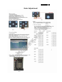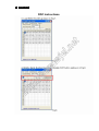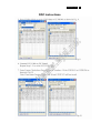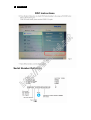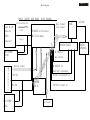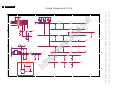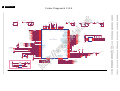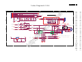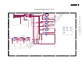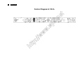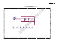
1
Chassis: HUDSON 9 22 inch TFT WXGA LCD Colour Monitor el. ne t 220S W 9F S /00 220S W 9F B /69 220S W 9F B /00 220S W 9F B /75 220S W 9F B /93 Horizontal frequencies 30 - 8 3 kHz TABLE OF CONTENTS Description Page Failure Mode Of Panel - ----------------------------------29 Wiring Diagram--------------------------------------------30 Block Diagram----------------------------------------------31 tp :// ww w. wj Description Page Important Safety Notice-------------------------------------2 Technical Data--------------------------------------------- 3~4 Installation------------------------------------------------------5 T roubleshooting-----------------------------------------------6 On Screen Display-----------------------------------------7~8 Lock/unlock, Aging,Factory mode-------------------------9 Philips Pixel Defect Policy ---------------------------------10 Mechanical Instructions -----------------------------11~12 Color adjustment -------------------------------------------13 F AQs (Frequently Asked Questions)--------------14~15 Electrical instruction ---------------------------------16~17 DDC Instructions & Serial Number ----------------18~24 DDC DATA ----------------------------------------------25~26 Firmware Upgrade for CPU- ------------------------27~28 SAFETY Scaler Diagram & C.B.A. ----------------------------32~38 Power Diagram & C.B.A. ---------------------------39~42 Control Diagram & C.B.A. ---------------------------43~44 LED Diagram & C.B.A. ---------------------------45~46 General product specification----------------------47~73 Exploded V iew ---------------------------------------------74 Spare/ Recommended P arts List----------------------75 PCBA photos------------------------------------------------76 Repair tips----------------------------------------------77~78 Repair Flow chart-------------------------------------79~81 Safety Test Requirments---------------------------------82 NOTICE ht ANY PERSON ATTEMPTING TO SERVICE THIS CHASSIS MUST FAMILIARIZE HIMSELF WITH THE CHASSIS AND BE AWARE OF THE NECESSARY SAFETY PRECAUTIONS TO BE USED WHEN SERVICING ELECTRONIC EQUIPMENT CONTAINING HIGH VOL TAGES. CAUTION: USE A SEPARATE ISOLATION TRANSFORMER FOR THIS UNIT WHEN SERVICING. REFER TO BACK COVER FOR IMPORTANT SAFETY GUIDELINES Published by Philips Consumer Lifestyle Copyright reserved Subject to modification JJun.9. 2008 GB 312278517980 Important Safety Notice LCD 2 2 220SW9 220BW 8 LCD Proper s ervic e and repair is important to the safe, reliable FOR PRODUCTS CONTAINING LASER : operation of all Philips Consumer Electronics Company DANGER - equipment. The service procedures recommended by Philips and described in this service manual a re eff ective methods of Invisible laser radiation when open. AVOID DIRECT EXPOSURE TO BEAM. performing service operations . Some of these service CAUTION - operations require the us e of tools speciall y desi gned for the Use of controls or adjustments or performance of procedures other than purpose. The special tools should be used when and as those specified herein may result in recomm ended. hazardous radiation exposure. It is im portant to note that this m anual c ontains various CAUTION - CAUTI ONS and NOTICES which should becarefully read in The use of optical instruments with this product will increase eye hazard. order to m inimize the risk of personal injury to service personnel . The possibility exists that improper service methods may damage the equipment. It is also important to t underst and that these CAUTIONS and NOTICES ARE NOT ne EXHAU STIVE. Philips could not possibly know, evaluate and TO ENSURE THE CONTINUED RELIABILITY OF THIS advise the servic etrade of all conceivable ways i n which PRODUCT , USE ONLY ORIGINAL MANUFACTURER'S consequences of each way. Consequently, Philips has not REPLACEMENT PAR TS, WHICH ARE LISTED WITH THEIR PART undertaken any such broad evaluation. Accordingly, NUMBERS IN THE PARTS LIST SECTION OF THIS who uses a servi ce procedure or tool which is not SERVICE MANUAL. neither his safety nor the safe operation of the equipment will be jeopardized by the service method selected. * * Hereafter throughout this manual, Philips Consumer Electronics Company will be referred to as Philips . * * w. wj recommended by Philips must first satisfy himself thoroughly that el. service might be done or of the possible hazardous ww Take care during handling the LCD module with backlight unit - Must mount the module using mounting holes arranged in four WARNING :// corners. Critical components having special safety characteristics are enclosed within a broken line tp identified with a by the Ref. No. in the parts list and (where several critical components are grouped in one area) exploded views. ht along with the safety symbol on the schematics or - Do not press on the panel, edge of the frame strongly or electric shock as this will result in damage to the screen. - Do not scratch or press on the panel with any sharp objects, such as pencil or pen as this may result in damage to the panel. - Protect the module from the ESD as it may damage the electronic circuit (C -MOS). Use of substitute replacement parts which do not have the - Make certain that treatment body are grounded through same speci fied safety characteristic s may create shock, fire, wrist band. or other hazards . - Do not leave the module in high temperature and in areas of high Under no circumstances should the original design be humidity for a long time. modified or altered without written permission from Philips. Philips assumes no liability, express or implied, arising out of any unauthorized modification of design. Servicer assumes all liability. - Avoid contact with water as it may as hort circuit within the module. - If the surface of panel become dirty, please wipe it off with a soft material. (Cleaning with a dirty or rough cloth may damage the panel.) 220SW9 LCD 3 Technical Data PIN No. SIGNAL Red 9 DDC +3.3V or +5V 2 Green/ SOG 10 Logic GND 3 Blue 11 Sense (GND) 4 Sense (GND) 12 Bi-directional data 5 Cable Detect (GND) 13 H/H+V sync 6 Red GND 14 V-sync 7 Green GND 15 Data clock 8 Blue GND Ambient temperature: 0 °C - 40 °C Power input connection The monitor must comply with the Microsoft On Now specification, and meet EPA requirements. HSYNC VSYNC Video Pwr-cons. Indication Power-On On On active 45TYP Blue LED -- Off Off Off blanked <1W Blanking Blue LED <3s tp :// Mode Rec. time N/A <1W ht DC Power Off el. Pin No. Description 1 T.M.D.S. data2- 2 T.M.D.S. data2+ 3 4 T.M.D.S. data2 shield No Connect 5 6 7 No Connect DDC clock DDC data 8 9 No Connect T.M.D.S. data1- 10 11 T.M.D.S. data1+ T.M.D.S. data1 shield 12 No Connect 13 14 No Connect +5V Power 15 16 Ground (for +5V) Hot plug detect 17 18 19 T.M.D.S. data0T.M.D.S. data0+ T.M.D.S. data0 shield 20 21 No Connect No Connect 22 23 T.M.D.S clock shield T.M.D.S. clock+ 24 T.M.D.S. clock- ww Power cord length : 1.8 M Power cord type : 3 leads power cord with protective earth plug. Power management ʳ ʳ ʳ ʳ nput DVI-D connector pin w. wj : 30 – 83 K Hz : 56 - 76 Hz : < 210 MHz for VGA and < 170 MHz for DVI, warning message must be displayed while over 165 MHz (supplier to provide accurate scaler bandwidth number) Power input : 90-264 V AC, 50/60 ± 2 Hz Power consumption : <50W maximum, <45W ( typ.) < TBDWatt (with audio) SIGNAL 1 Scanning frequencies Hor. Ver. Video dot rate PIN No. t : SEC LTM220M1-L01 : 1680 x 1050 (WSXGA+) : 493.7(H) x 320.1(V) Typ. x 17.0(D) Max. : 0.282mm x 0.282mm : RGB vertical stripe : Haze 25% Hard coating (3H) : 16.7M (6 bit Hi-FRC) : 4 CCFL : 473.76(H) x 296.1(V) mm : =160 for Right/Left (Typ) : =160 for Up/Down (Typ) Contrast ratio : 1000:1 (Typ) White luminance : 300(Typ.) Color gamut : >=72% Gate IC : TOSHIBA Source IC : NEC Response time : Tr + Tf <=5 ms (Typ) Vertical frequency range: 53~76Hz ne SEC panel Type NR. Resolution Outside dimensions Pitch (mm) Color pixel arrangement Display surface Color depth Backlight Active area (W x H) View angle (CR=10) LED Off Susceptibility of display to external environment Operating - Temperature : 0 to 40 degree C - Humidity : 80% max - Altitude : 0-3658m - Air pressure : 600-1100 mBAR Storage - Temperature - Humidity - Altitude - Air pressure : -20 to 60 degree C : 95% max : 0-12192m : 300-1100 mBAR Note: recommend at 5 to 35°C, Humidity less than 60 % 220SW9 L CD Tec hnic al Data LPL Panel Type NR . R es olution Outs ide dimens ions P IN No. S IG NAL : LP L LM220W E 1-T LE 2/4 : 1680 x 1050 (W S XG A+) 1 R ed : 493.7(H) x 320.1 (V ) x 16.5(D) mm (Typ.) 2 G reen/ S OG P itch (mm) : 0.282mm x 0.282mm C olor pixel arrangement : 1680 horizontal B y 1050 3 B lue vertical P ixels R G B stripe arrangement 4 S ens e (G ND) Dis play s urface : Hard coating (3H), Anti-glare treatment of the front polarizer 5 C able Detect (G ND) C olor depth : 16.7M colors B acklight : 4 CCFL 6 R ed G ND Active area (W x H) : 21.995 inches (558.673mm) diagonal 7 G reen G ND As pect(ratio 16:10) 8 B lue G ND View angle (C R >=10) : R /L 170(Typ.), U/D 160(Typ.) C ontras t ratio : >1000:1 (Typ) nput DVI-D connector pin W hite luminance : 300 cd/m2(Typ. C enter 1 point) C olor gamut : >=72% G ate IC : N/A S ource IC : Magna , OK I R es pons e time : <=5 ms (Typ) Vertical frequency range: 50~75Hz P IN No. S IG NAL DDC +3.3V or +5V 10 Logic G ND 11 S ens e (G ND) 12 B i-directional data 13 H/H+V s ync 14 V -s ync 15 Data clock ne t 9 el. P in No. : 30 – 83 K Hz : 56 - 76 Hz : < 210 MHz for V G A and < 170 MHz for DV I, warning mess age must be dis played while over 165 MHz (s upplier to provide accurate scaler bandwidth number) P ower input : 90-264 V AC , 50/60 ± 2 Hz P ower cons umption : <50W maximum, <45W ( typ.) < T B DWatt (with audio) ww Hor. Ver. Video dot rate Ambient temperature: 0 C - 40 C :// P ower input c onnec tion tp P ower cord length : 1.8 M P ower cord type : 3 leads power cord with protective earth plug. Power management T he monitor mus t comply with the Micros oft On Now s pecification, and meet E PA requirements. Mode HS Y N C VS YN C Video P wr-con s. P owerOn On On active 45T Y P Off Off Off DC P ower Off blanked N/A Des c ription w. wj S c anning frequenc ies ht 4 <1W <1W Indicati on B lue LE D B lankin g B lue LE D LE D Off Re c. tim e -<3 s 1 T .M.D.S . data2- 2 T .M.D.S . data2+ 3 4 5 6 T .M.D.S . data2 s hield No C onnect No C onnect DDC clock 7 8 9 DDC data No C onnect T .M.D.S . data1- 10 T .M.D.S . data1+ 11 12 13 14 T .M.D.S . data1 s hield No C onnect No C onnect +5V P ower 15 16 17 18 G round (for +5V ) Hot plug detect T .M.D.S . data0T .M.D.S . data0+ 19 20 21 22 23 T .M.D.S . data0 s hield No C onnect No C onnect T .M.D.S clock s hield . T M.D.S . clock+ 24 ıT.M.D.S clock S us c eptibility of dis play to external en v ironment Operating - T emperature - Humidity - Altitude - Air pres s ure S torage - T emperature - Humidity - Altitude - Air pres s ure : 0 to 40 degree C : 80% max : 0-3658m : 600-1100 mB AR : -20 to 60 degree C : 95% max : 0-12192m : 300-1100 mB AR Note: recommend at 5 to 35°C , Humidity less than 60 % 220SW9 LCD 5 Installation Accessory Pack Front View Product Description Unpack all the parts ʳ ʳ Power cord ʳ t DVI cable (Optional) ne ʳ VGA cable ʳ To switch monitor's power On and Offʳ 1 ʳ ʳ 3 Connecting to Your PC To adjust the OSD menu ʳ . 1) Connect the power cord to the back of the monitor firmly. (Philips has pre-connected VGA cable for the first installation. w. wj ʳ To access OSD menuʳ el. 2 EDFU packʳ To adjust brightness of the displayʳ 4 ʳ To change the signal input source. ʳ 5 Inputʳ Automatically adjust the horizontal position, ʳ vertical position phase and clock settings / Return to previous OSD level. ʳ 7 SmartImage. There are five modes to be selected: Office Work, Image Viewing, Entertainment Economy, and Off.ʳ ʳ ww 6 *available for selective modelsʳ ht tp :// Rear View *available for selective modelsʳ ʳ ʳ 1ʳ VGA inputʳ 2ʳ DVI-D input (available for selective models) ʳ 3ʳ AC power inputʳ 4ʳ Kensington anti-thief lockʳ 2) Connect to PCʳ (a)ʳ Turn off your computer and unplug its power cable. (b)ʳ Connect the monitor signal cable to the video connector on the back of your computer.ʳ (c)ʳ Plug the power cord of your computer and your monitor into a nearby outlet.ʳ (d)ʳ Turn on your computer and monitor. If the monitor displays an image, installation is complete.ʳ ʳ 220SW9 L CD tp :// ww w. wj el. ne t Trouble s hooting ht 6 220SW 9 L CD 7 On S c reen Dis play Des c ription of the On S c reen Dis play What is the On-Screen Display? ww w. wj el. ne t On-S creen Dis play (O S D) is a feature in all P hilips LC D monitors . It allows an end us er to adjus t s creen performance or s elect functions of the monitors directly through an on-s creen ins truction window. A us er friendly on s creen dis play interface is s hown as below : :// B as ic and s imple ins truc tion on the c ontrol keys . In the OS D s hown above us ers can pres s to confirm the choice or change. ht tp move the curs or, buttons at the front bezel of the monitor to 8 220SW9 LCD On Screen Display The OSD Tree ht tp :// ww w. wj el. ne t Below is an overall view of the structure of the On-Screen Display. You can use this as a reference when you want to work your way around the different adjustments later on. ʳ Resolution notification This monitor is designed for optimal performance at its native resolution, 1680X1050@60Hz. When the monitor is powered on at a different resolution, an alert is displayed on screen: Use 1680x1050@60Hz for best results.ʳ ˗˼̆̃˿˴̌ʳ̂˹ʳ̇˻˸ʳ́˴̇˼̉˸ʳ̅˸̆̂˿̈̇˼̂́ʳ˴˿˸̅̇ʳ˶˴́ʳ˵˸ʳ̆̊˼̇˶˻˸˷ʳ̂˹˹ʳ˹̅̂̀ʳ˦˸̇̈̃ʳ˼́ʳ̇˻˸ʳˢ˦˗ʳʻˢ́ʳ˦˶̅˸˸́ʳ˗˼̆̃˿˴̌ʼʳ̀˸́̈ˁʳ 220SW9 LCD 9 ht tp :// ww w. wj el. ne t Lock/Unlock, Aging,Factory Mode 10 220SW 9 L CD P hilips P ixel Defec t P olic y P hilips ' F lat P anel Monitors P ixel Defec t P olic y B lack Dot Defects B lack dot defects appear as pixels or s ub pixels that are always dark or 'off'. T hat is, a dark dot is a s ub-pixel that s tands out on the s creen when the monitor dis plays a light pattern. T hes e are the types of black dot defects T wo or three adjacent dark s ub pixels t One dark s ub pixel ne P hilips s trives to deliver the highes t quality products . W e us e s ome of the industry's mos t advanced manufacturing proces s es D and practice s tringent quality control. However, pixel or s ub pixel defects on the T F T LC D panels us ed in flat panel monitors are s ometimes unavoidable. No manufacturer can guarantee that all panels will be free from pixel defects , but P hilips guarantees that any monitor with an unacceptable number of defects will be repaired or replaced under warranty. T his notice explains the different types of pixel defects and defines acceptable defect levels for each type. In order to qualify for repair or replacement under warranty, the number of pixel defects on a T F T LC D panel must exceed thes e acceptable levels . F or example, no more than 0.0004% of the s ub pixels on a 19" XG A monitor may be defective. F urthermore, P hilips s ets even higher quality s tandards for certain types or combinations of pixel defects that are more noticeable than others . T his policy is valid worldwide. P roximity of P ixel Defec ts el. B ecaus e pixel and s ub pixels defects of the s ame type that are near to one another may be more noticeable, P hilips als o s pecifies tolerances for the proximity of pixel defects P ixel Defec t Toleranc es w. wj In order to qualify for repair or replacement due to pixel defects during the warranty period, a T F T LC D panel in a P hilips flat panel monitor must have pixel or sub pixel defects exceeding the tolerances lis ted in the following tables . P ixels and S ub pix els B R IG HT DOT DE F E C T S AC C E P T AB L E L E VE L 220S W 9 MODE L ww A pixel, or picture element, is compos ed of three s ub pixels in the primary colors of red, green and blue. Many pixels together form an image. W hen all s ub pixels of a pixel are lit, the three colored s ub pixels together appear as a s ingle white pixel. W hen all are dark, the three colored s ub pixels together appear as a s ingle black pixel. Other combinations of lit and dark s ub pixels appear as s ingle pixels of other colors . Types of P ixel Defec ts :// P ixel and s ub pixel defects appear on the screen in different ways . T here are two categories of pixel defects and s everal types of s ub pixel defects within each category. ht tp B right Dot Defects B right dot defects appear as pixels or s ub pixels that are always lit or 'on'. T hat is , a bright dot is a s ub-pixel that stands out on the s creen when the monitor dis plays a dark pattern. T here are the types of bright dot defects : T wo adjacent lit s ub pixels : - R ed + B lue = T hree adjacent lit s ub One lit red, green or P urple pixels (one white blue s ub pixel - R ed + G reen = pixel) Y ellow - G reen + B lue = C yan (Light B lue) A red or blue bright dot mus t be more than 50 percent brighter than neighboring dots while a green bright dot is 30 percent brighter than neighboring dots . 1 lit s ubpixel 3 2 adjacent lit s ubpixels 1 3 adjacent lit s ubpixels (one white pixel) 0 Dis tance between two bright dot defects * >25mm T otal bright dot defects of all types B L AC K DO T DE F E C T S 3 AC C E P T AB L E L E VE L 220S W 9 MODE L 1 dark s ubpixel 5 2 adjacent dark s ubpixels 2 3 adjacent dark s ubpixels 0 Dis tance between two black dot defects * >15mm T otal black dot defects of all types 5 T OTAL DOT DE F E C T S AC C E P TAB LE LE VE L MODE L 220S W 9 Total bright or black dot defects of all types 5 Note: * 1 or 2 adjacent s ub pixel defects = 1 dot defect 220SW9 LCD Mechanical Instruction Front view ne t Step3. Remove the back cover by using 2 release holes. ww Step1. Remove base by pushing the release button. w. wj el. Back view ht tp :// Step4. Release lamp wire from power board. Step2. Unscrew 4 screws to release the neck column. Step5. Release control board and led board cable. 11 12 220SW9 LCD Mechanical Instruction Step9. Unscrew 7 screws to release power board and interface board. el. ne t Step6. Unscrew 2 screws to remove the main shielding w. wj Step10. Unscrew 3 screws to release control board. ht tp :// ww Step7. Release the main shielding by pushing the metal part. Step8. Take the LVDS cable off from panel. Step11. Remove the led board by hand carefully. 220SW9 LCD 13 ht tp :// ww w. wj el. ne t Color Adjustment 14 220SW 9 L CD D FAQs (F requently As ked Ques tionis ) Q: W hat does the R efres h R ate mean for L C D? Q: Will the L C D s c reen be res is tant to s c ratc hes ? t A: A protective coating is applied to the s urface of the LC D, which is durable to a certain extent (approximately up to the hardnes s of a 2H pencil). In general, it is recommended that the panel s urface is not s ubject to any exces s ive s hocks or s cratches . Q: How s hould I c lean the L C D s urfac e? ne Q: W hat does 'refres h rate' mean in c onnec tion with an L C D monitor? A: F or normal cleaning, us e a clean, s oft cloth. F or extens ive cleaning, pleas e us e is opropyl alcohol. Do not us e other s olvents s uch as ethyl alcohol, ethanol, acetone, hexane, etc. Q: C an I c hange the color s etting of my monitor? A: Your video card/graphic driver and monitor together determine the available res olutions . You can s elect the des ired res olution under W indows ® C ontrol P anel with the "Dis play properties". A: Yes , you can change your color s etting through OS D control as the following procedures , 1. P res s "OK " to s how the OS D (On S creen Dis play) menu 2. P res s "Down Arrow" to s elect the option "C olor" then press "OK " to enter color s etting, there are three s ettings as below. a. C olor Temperature; T he six s ettings are 5000K , 6500K , 7500K , 8200K , 9300K and 11500K . W ith s ettings in the 5000K range the panel appears ‘warm,' with a red-white color tone, while a 11500K temperature yields ‘cool, blue-white toning." b. s R G B ; this is a standard s etting for ens uring correct exchange of colors between different device (e.g. digital cameras , monitors, printers , scanners, etc) c. Us er Define; the us er can choose his/her preference color s etting by adjus ting red, green blue color. d. G amma; T he five s ettings are 1.8, 2.0, 2.2, 2.4, and 2.6. *A meas urement of the color of light radiated by an object while it is being heated. T his meas urement is expres s ed in terms of abs olute s cale, (degrees K elvin). Lower K evin temperatures s uch as 2004K are red; higher temperatures s uch as 9300K are blue. Neutral temperature is white, at 6504K . Q: W hat if I get los t when I am making monitor adjus tments ? Q: C an the P hilips L C D Monitor be mounted on the wall? A: S imply press the OK button, then s elect 'R es et' to recall all of the original factory s ettings . A: Yes . P hilips LC D monitors have this optional feature. F or s tandard VE S A mount holes on the rear cover allows the us er to mount the P hilips monitor on mos t of the V E S A standard arms or acces s ories . W e recommend to contact your P hilips s ales repres entative for more information. w. wj A: T he refres h rate is of much less relevance for LC D monitors . LC D monitors dis play a s table, flicker-free image at 60Hz. T here is no vis ible difference between 85Hz and 60Hz. Q: W hat are the .inf and .icm files on the C D-R OM? How do I ins tall the drivers (.inf and .icm)? tp :// Q: How do I adjus t the res olution? ww A: T hes e are the driver files for your monitor. F ollow the ins tructions in your us er manual to install the drivers. Your computer may ask you for monitor drivers (.inf and .icm files ) or a driver dis k when you firs t ins tall your monitor. F ollow the ins tructions to ins ert the ( companion C D-R OM) included in this package. Monitor drivers (.inf and .icm files ) will be ins talled automatically. ht D A: R ecommended video mode for P hilips 22": 1680x1050 @ 60Hz. 1. Unplug all cables , then connect your P C to the monitor that you us ed previous ly. 2. In the W indows S tart Menu, s elect S ettings /C ontrol P anel. In the C ontrol P anel W indow, s elect the Dis play icon. Ins ide the Dis play C ontrol P anel, s elect the 'S ettings ' tab. Under the s etting tab, in box labeled 'desktop area', move the s lidebar to 1680x1050 pixels (22"). 3. Open 'Advanced P roperties ' and s et the R efres h R ate to 60Hz, then click OK . 4. R es tart your computer and repeat step 2 and 3 to verify that your P C is s et at 1680x1050@ 60Hz (22"). 5. S hut down your computer, disconnect your old monitor and reconnect your P hilips LC D monitor. 6. Turn on your monitor and then turn on your P C . A: Unlike C R T dis play technology, in which the s peed of the electron beam is s wept from the top to the bottom of the screen determines flicker, an active matrix dis play us es an active element (T F T ) to control each individual pixel and the refres h rate is therefore not really applicable to LC D technology. el. G eneral FAQs Q: W hen I ins tall my monitor what s hould I do if the s c reen s hows 'C annot dis play this video mode'? Q: W hat is the Auto func tion? A: T he AUT O adjus tment key res tores the optimal s creen pos ition, phas e and clock s ettings by pres s ing of a single button – without the need to navigate through OS D (On S creen Dis play) menus and control keys . Note: Auto function is available in s elected models only. S c reen Adjus tments Q: W hen I ins tall my monitor, how do I get the bes t performanc e from the monitor? Q: My Monitor has no power (P ower L E D does not light up). W hat s hould I do? A: F or bes t performance, make s ure your dis play s ettings are s et at 1680x1050@ 60Hz for 22". Note: You can check the current dis play s ettings by press ing the OS D OK button once. T he current dis play mode is s hown in OS D s etup information page A: Make s ure the AC power cord is connected between the monitor and AC outlet, and click a key on keyboard/mous e to wake up the P C . Q: How do L C Ds c ompare to C R Ts in terms of radiation? Q: Will the L C D monitor ac c ept an interlac ed s ignal under P C models ? A: No. If an Interlace s ignal is us ed, the screen dis plays both odd and even horizontal scanning lines at the s ame time, thus dis torting the picture. A: B ecaus e LC Ds do not us e an electron gun, they do not generate the s ame amount of radiation at the screen s urface. C ompatibility with other P eripherals Q: C an I c onnec t my L C D monitor to any P C , works tation or Mac? A: Yes . All P hilips LC D monitors are fully compatible with s tandard P C s , Macs and workstations . You may need a cable adapter to connect the monitor to your Mac s ystem. P leas e contact your P hilips s ales repres entative for more information. 220SW 9 L CD 15 FAQs (F requently As ked Ques tionis ) Q: Are P hilips L C D monitors P lug-and-P lay? Q: W hy is vertic al frequenc y of 60Hz optimal for an L C D monitor? A: T he T F T LC D panel is an element that controls /dis plays the inlet of a backlight using the dual-refraction of a liquid crys tal. Us ing the property that the projection of inlet light refracts toward the major axis of the liquid element, it controls the direction of inlet light and dis plays it. S ince the refraction ratio of inlet light on liquid crys tal varies with the inlet angle of the light, the viewing angle of a T F T is much narrower than that of a C DT. Us ually, the viewing angle refers to the point where the contrast ration is 10. Many ways to widen the viewing angle are currently being developed and the mos t common approach is to us e a wide viewing angle film, which widens the viewing angle by varying the refraction ratio. IP S (In P lane S witching) or MVA (Multi Vertical Aligned) is als o us ed to give a wider viewing angle. w. wj Q: W hat is a US B hub ? Q: W hat kind of wide-angle tec hnology is available? How does it work? t A: T hink of US B as a smart plug for P C peripherals. US B automatically determines res ources (like driver s oftware and bus bandwidth) required by peripherals . US B makes necess ary res ources available without us er intervention. T here are three main benefits of US B . US B eliminates "cas e anxiety," the fear of removing the computer cas e to install circuit board cards -- that often requires adjustment of complicated IR Q s ettings -- for add-on peripherals . US B does away with "port gridlock." W ithout US B , P C s are normally limited to one printer, two C om port devices (us ually a mous e and modem), one E nhanced P arallel P ort add-on (s canner or video camera, for example), and a joys tick. More and more peripherals for multimedia computers come on the market every day. W ith US B , up to 127 devices can run s imultaneous ly on one computer. US B permits "hot plug-in." No need to s hut down, plug in, reboot and run s et up to ins tall peripherals . No need to go through the revers e proces s to unplug a device. B ottom line: US B transforms today's "P lug-and-P ray" into true P lug-and-P lay! P leas e refer to glos s ary for more information about US B . ne Q: W hat is US B (Univers al S erial B us )? A: Unlike a C DT monitor, the T F T LC D panel has a fixed res olution. F or example, an XG A monitor has 1024x3 (R , G, B ) x 768 pixels and a higher res olution may not be available without additional s oftware proces s ing. T he panel is designed to optimize the dis play for a 65MHz dot clock, one of the s tandards for XG A dis plays. S ince the vertical/horizontal frequency for this dot clock is 60Hz/48kHz, the optimum frequency for this monitor is 60Hz. el. A: Yes , the monitors are P lug-and-P lay compatible with W indows ® 95, 98, 2000, XP and Vis ta. Q: W hy is there no flic ker on an L C D Monitor? A: A US B hub provides additional connections to the Univers al S erial B us. A hub's upstream port connects a hub to the host, us ually a P C . Multiple downs tream ports in a hub allows connection to another hub or device, s uch as a US B keyboard, camera or printer. Q: W hat is a L iquid C rys tal Dis play? ww L C D P anel Tec hnology A: Technically s peaking, LC Ds do flicker, but the caus e of the phenomenon is different from that of a C R T monitor -- and it has no impact of the eas e of viewing. F lickering in an LC D monitor relates to us ually undetectable luminance caus ed by the difference between pos itive and negative voltage. On the other hand, C R T flickering that can irritate the human eye occurs when the on/off action of the fluores cent object becomes vis ible. S ince the reaction s peed of liquid crystal in an LC D panel is much s lower, this troubles ome form of flickering is not pres ent in an LC D dis play. tp :// A: A Liquid C rys tal Dis play (LC D) is an optical device that is commonly us ed to dis play AS C II characters and images on digital items s uch as watches , calculators , portable game cons oles , etc. LC D is the technology us ed for dis plays in notebooks and other small computers . Like light-emitting diode and gas -plasma technologies , LC D allows dis plays to be much thinner than cathode ray tube (C R T ) technology. LC D cons umes much less power than LE D and gas -dis plays becaus e it works on the principle of blocking light rather than emitting it. Q: W hy is an L C D monitor virtually low of E lec tro Magnetic Interferenc e? A: Unlike a C R T, an LC D monitor does not have key parts that generate E lectro Magnetic Interference, es pecially magnetic fields. Als o, s ince an LC D dis play utilizes relatively low power, its power s upply is extremely quiet. E rgonomic s , E c ology and S afety S tandards A: An LC D is made with either a pas s ive matrix or an active matrix dis play grid. An active matrix has a trans istor located at each pixel inters ection, requiring les s current to control the luminance of a pixel. F or this reason, the current in an active matrix dis play can be s witched on and off more frequently, improving the screen refres h time (your mous e pointer will appear to move more smoothly acros s the screen, for example). T he pass ive matrix LC D has a grid of conductors with pixels located at each inters ection in the grid. A: T he C E (C onformité E uropéenne) mark is required to be dis played on all regulated products offered for s ale on the E uropean market. T his 'C E ' mark means that a product complies with the relevant E uropean Directive. A E uropean Directive is a E uropean 'Law' that relates to health, s afety, environment and cons umer protection, much the s ame as the U.S . National E lectrical C ode and UL S tandards. ht Q: W hat differentiates pas s ive matrix L C Ds from ac tive matrix L C Ds ? Q: W hat are the advantages of T F T L C D c ompared with C R T? A: In a C R T monitor, a gun s hoots electrons and general light by colliding polarized electrons on fluores cent glass. T herefore, C R T monitors bas ically operate with an analog R G B s ignal. A T F T LC D monitor is a device that dis plays an input image by operating a liquid crystal panel. T he T F T has a fundamentally different structure than a C R T: E ach cell has an active matrix s tructure and independent active elements. A T F T LC D has two glas s panels and the s pace between them is filled with liquid crys tal. W hen each cell is connected with electrodes and impress ed with voltage, the molecular s tructure of the liquid crys tal is altered and controls the amount of inlet lighting to dis play images . A T F T LC D has s everal advantages over a C R T, s ince it can be very thin and no flickering occurs becaus e it does not us e the scanning method. Q: W hat is the C E mark? Q: Does the L C D monitor c onform to general s afety s tandards ? A: Yes . P hilips LC D monitors conform to the guidelines of MP R -II and T C O 99/03 standards for the control of radiation, electromagnetic waves , energy reduction, electrical s afety in the work environment and recyclability. T he s pecification page provides detailed data on s afety s tandards . Q: After I c hange new P C , I found this information on s c reen, how c an I do? A: B ecaus e you activate T heft Deterrence function in S martC ontrol II. P leas e contact IT manager or P hilips S ervice C enter. 16 220SW9 LCD Electrical Instructions 1.Electrical Characteristics 1.1 Interface signals 1). D-Sub Analog Input signal : Video, Hsync., Vsync Video : 0.7 Vp-p, input impedance, 75 ohm @DC Sync. : Separate sync TTL level , input impedance 2.2k ohm terminate Hsync Positive/Negative Vsync Positive/Negative Composite sync TTL level, input impedance 2.2k ohm terminate (Positive/Negative) Sync on green video 0.3 Vp-p Negative (Video 0.7 Vp-p Positive) ne t 2). DVI-D Digital Input signal: Single TMDS link (Three channels: RX0-/+, RX1-/+, RX2-/+) w. wj el. 1.2 Interface D-Sub Cable Length : 1.8 M +/- 50 mm Fix with monitor when packing, with transplant pin protective cover. Connector type : D-Sub male with DDC2B pin assignments. Blue connector thumb-operated jack screws 1.3 Timing requirement 1.3.1 Mode storing capacity Factory preset modes : D-sub :18 , DVI : 17 Preset modes : 49 User modes : 10 ht tp :// ww 1.3.2 Factory preset modes ( D-sub18 modes) 220SW9 LCD 17 ht tp :// ww w. wj el. ne t Electrical Instructions 18 220SW9 LCD ht tp :// ww w. wj el. ne t DDC Instructions 220SW9 LCD 19 ht tp :// ww w. wj el. ne t DDC Instructions 20 220SW9 LCD ht tp :// ww w. wj el. ne t DDC Instructions 220SW9 LCD 21 ht tp :// ww w. wj el. ne t DDC Instructions 22 220SW9 LCD ht tp :// ww w. wj el. ne t DDC Instructions 220SW9 LCD 23 ht tp :// ww w. wj el. ne t DDC Instructions 24 220SW9 LCD ww w. wj el. ne t DDC Instructions ht tp :// Serial Number Definition 220SW 9 L CD 25 DDC DATA 1 2 3 4 5 6 0: 00 10: 6F 20: 0E 30: 9A 40: 81 50: A9 60: 27 70: 00 80: 30 90: 00 100: 70 110: 00 120: 20 FF 08 2F 25 80 40 40 1E 37 00 73 FD 20 FF 01 1D 12 81 A9 68 00 31 00 20 00 20 FF 00 78 50 8F 4F B0 00 35 FC 32 38 20 FF 00 EE 54 95 08 36 00 30 00 32 4C 20 FF 00 B5 BF 00 39 00 FF 30 50 30 1E 20 FF 07 05 EF 95 90 DA 00 30 68 53 53 00 7 8 9 00 41 0C 12 01 03 A5 56 4A 80 B 3 00 0F B 3 0F 30 62 1A 28 11 00 43 53 33 30 30 31 69 6C 69 57 00 00 11 00 0A 09 Decoded E DID data <---Header---> Header: <-x-Header-x-> ww <---Vendor/P roduct Identification---> ID Manufacturer Name: P HL ID P roduct C ode: 086F ID S erial Number: 00000001 W eek of Manufacture: 7 Year of Manufacture: 2008 <-x-Vendor/P roduct Identification-x-> :// <---E DID S tructure Vers ion/R evis ion---> E DID Vers ion#: 1 E DID R evis ion#: 3 <-x-E DID S tructure Vers ion/R evis ion-x-> ht tp <---B as ic Dis play P arameters/F eatures ---> Video i/p definition: Analog S etup: B lank-to-B lack not expected S eperate S yncs . s upport: Yes C ompos ite S ync. s upport: Yes Vs ync. P uls e: s erration required Max Horz Image S ize: 47 cm. Max Vert Image S ize: 29 cm. Dis play G amma: 2.2 Dis play Type: R G B color dis play S tandard Default C olor S pace: Yes F eatures, P referred Timing Mode: In first detailed block F eatures, G T F s upport: No DP MS F eatures, S tand-by: Yes DP MS F eatures, S us pend: Yes DP MS F eatures, Active Off: Yes <-x-B as ic Dis play P arameters /F eatures -x-> <---C olor C haracteris tics ---> R ed x: 0.646484 R ed y: 0.338867 G reen x: 0.290039 G reen y: 0.602539 B lue x: 0.144531 B lue y: 7.03125e-002 W hite x: 0.313477 W hite y: 0.329102 <-x-C olor C haracteris tics -x-> <---S tandard Timing Identification---> S tandard Timing: 1680x1050 @ 60Hz S tandard Timing: 1280x1024 @ 60Hz S tandard Timing: 1280x1024 @ 75Hz S tandard Timing: 1440x 900 @ 60Hz S tandard Timing: 1440x 900 @ 75Hz S tandard Timing: 1680x1050 @ 75Hz S tandard Timing: 1600x1200 @ 60Hz S tandard Timing: 1600x1200 @ 75Hz <-x-S tandard Timing Identification-x-> w. wj 00 F F F F F F F F F F F F 00 t 0 ne 128 bytes E DID Data (Hex): <---E s tablis hed Timings ---> E s tablis hed Timimgs 1: B F - 720x400 @ 70Hz - 640x480 @ 60Hz - 640x480 @ 67Hz - 640x480 @ 72Hz - 640x480 @ 75Hz - 800x600 @ 56Hz - 800x600 @ 60Hz E s tablis hed Timimgs 2: E F - 800x600 @ 72Hz - 800x600 @ 75Hz - 832x624 @ 75Hz - 1024x768 @ 60Hz - 1024x768 @ 70Hz - 1024x768 @ 75Hz - 1280x1024 @ 75Hz - 1152x870 @ 75Hz E s tablis hed Timings 3: 80 <-x-E s tablis hed Timings -x-> el. //////////Dis playing Monitor E DID////////// <---Detailed Timing Descriptions ---> Detailed Timing: 1680x1050 @ 59Hz Detailed Timing: F F (Monitor S N) 'C S 30715000001' Detailed Timing: F C (Monitor name) 'P hilips 220S W ' Detailed Timing: F D (Monitor limits ) Vert: 56 - 76 Hz Horz: 30 - 83 K Hz C lk: 170 MHz <-x-Detailed Timing Descriptions -x-> E xtens ion F lag: 00 C hecks um: 09 26 220SW 9 L CD DDC DATA 0 1 2 3 4 5 6 7 8 0: 00 10: 6F 20: 80 30: 9A 40: 81 50: 01 60: 1E 70: 00 80: 30 90: 00 100: 70 110: 00 120: 20 FF 08 2F 25 80 01 40 1A 37 00 73 FD 20 FF 01 1D 12 81 01 30 00 31 00 20 00 20 FF 00 78 50 8F 01 20 00 35 FC 32 38 20 FF 00 EE 54 95 7C 36 00 30 00 32 4C 20 FF 00 B5 BF 00 2E 00 FF 30 50 30 1E 20 FF 07 05 EF 95 90 DA 00 30 68 53 53 00 00 12 A5 80 0F A0 28 43 30 69 57 11 4B 41 01 56 B3 A9 60 11 53 30 6C 00 00 9 0C 03 4A 00 40 1A 00 33 31 69 00 0A Decoded E DID data <---Header---> Header: <-x-Header-x-> ww <---Vendor/P roduct Identification---> ID Manufacturer Name: P HL ID P roduct C ode: 2159 ID S erial Number: 00000001 W eek of Manufacture: 7 Year of Manufacture: 2008 <-x-Vendor/P roduct Identification-x-> <---E DID S tructure Vers ion/R evis ion---> E DID Vers ion#: 1 E DID R evis ion#: 3 <-x-E DID S tructure Vers ion/R evis ion-x-> ht tp :// <---B as ic Dis play P arameters /F eatures ---> Video i/p definition: Analog S etup: B lank-to-B lack not expected S eperate S yncs . s upport: No C ompos ite S ync. s upport: No Vs ync. P uls e: s erration not required Max Horz Image S ize: 47 cm. Max Vert Image S ize: 29 cm. Dis play G amma: 2.2 Dis play Type: R G B color dis play S tandard Default C olor S pace: Yes F eatures, P referred Timing Mode: In first detailed block F eatures, G T F s upport: No DP MS F eatures, S tand-by: Yes DP MS F eatures, S us pend: Yes DP MS F eatures, Active Off: Yes <-x-B as ic Dis play P arameters /F eatures -x-> <---C olor C haracteris tics ---> R ed x: 0.646484 R ed y: 0.338867 G reen x: 0.290039 G reen y: 0.602539 B lue x: 0.144531 B lue y: 7.03125e-002 W hite x: 0.313477 W hite y: 0.329102 <-x-C olor C haracteris tics -x-> <---S tandard Timing Identification---> S tandard Timing: 1680x1680 S tandard Timing: 1280x1024 S tandard Timing: 1280x1024 S tandard Timing: 1440x1440 S tandard Timing: 1440x1440 S tandard Timing: 1600x1200 <-x-S tandard Timing Identification-x-> w. wj 00 F F F F F F F F F F F F 00 t 128 bytes E DID Data (Hex): <---E s tablis hed Timings ---> E s tablis hed Timimgs 1: B F - 720x400 @ 70Hz - 640x480 @ 60Hz - 640x480 @ 67Hz - 640x480 @ 72Hz - 640x480 @ 75Hz - 800x600 @ 56Hz - 800x600 @ 60Hz E s tablis hed Timimgs 2: E F - 800x600 @ 72Hz - 800x600 @ 75Hz - 832x624 @ 75Hz - 1024x768 @ 60Hz - 1024x768 @ 70Hz - 1024x768 @ 75Hz - 1280x1024 @ 75Hz - 1152x870x75Hz E s tablis hed Timings 3: 80 <-x-E s tablis hed Timings -x-> ne //////////Dis playing Monitor E DID////////// el. D @ 60Hz @ 60Hz @ 75Hz @ 60Hz @ 75Hz @ 60Hz <---Detailed Timing Descriptions ---> Detailed Timing: 1680x1050 @ 59Hz Detailed Timing: F F (Monitor S N) 'C S 30715000001' Detailed Timing: F C (Monitor name) 'P hilips 220S W ' Detailed Timing: F D (Monitor limits ) Vert: 56 - 76 Hz Horz: 30 - 83 K Hz C lk: 170 MHz <-x-Detailed Timing Descriptions -x-> E xtens ion F lag: 00 C hecks um: 4B 220SW 9 L CD 27 F irmware Upgrade for C P U tp :// ww S tep 3 : C hoose *.hex w. wj el. ne t S tep 1 : Ins tall “P ort95nt.exe” R es tart computer. S tep 2 : Dobule click “E as yUS B W riter\W riter_t9.exe” P res s “Load F ile” ht S tep 4 : P res s “Auto” to update F /W 28 220SW 9 L CD w. wj el. ne t F irmware Upgrade for C P U ht tp :// ww S tep 5 : Update O K !! 220SW9 LCD 29 ht tp :// ww w. wj el. ne t Failure Mode Of Panel Wiring Diagram ne t 220SW9 LCD CN701 .w j CN802 el. CN801 CN803 CN804 tp :// w ww CN551 ht 30 J1 J1 J6 J8 J3 J5 220SW9 LCD 31 Blo ck Dia gram PHILPS 220SW9 MAIN BOARD BLOCK DIAGRAM RIN.GIN.BIN HSYNC.VSYNC VGA-SCL Connector (DSUB connector) NT68667H with Internal MCU/Flash Memory el. Digital singal :// I2C BL-PWM for max current BL-BRIGHT for backlight adjustment tp DVI-SDA DATA EEPROM 2 4C16 LCD-ON for panel on 24C02 INVETER CIRCUIT BL-EN for backlight on ht DVI-D Connector ww w. wj DDC EEPROM 24C02 DDC EEPROM ne VGA-SDA DVI-SCL PANEL t Input R,G,B Dual channel lvds singal LCD-VDD Key board MOSFET APM2301A 220SW 9 L CD S c aler Diagram & C .B .A 1 2 3 4 5 H SI TP78 13 VSI TP79 14 VGA_SCL TP82 15 A GAITP74 GAI+ C1 BAITP75 BAI+ TP71 TP76 K DN3 J BAV99 0.1U Z C2 DN2 J BAV99 0.1U Z C3 0.1U Z ne t 12 TP70 RAI+ A TP81 DN1 J BAV99 RAI- 6 1 7 2 8 3 9 4 10 5 A VGA_SDA K K J1 11 A G1 +5V_ESD 100M/33ohm L1 Z30 R1 75 J RAI+ C4 G2 R2 C5 D-sub 15 TP77 4.7P C * RAI- R3 VGA_5V R5 1K J VGA_DET K R4 +5V_ESD D1 TZMC6V2 DN4 BAV99 R8 R6 C6 0.047U 16V 100 J C7 0.047U 16V RI1- RI1- SOGI 75 J C8 0.047U 16V GI1 C11 0.047U 16V GI1- C12 0.047U 16V A RI1 GI1 SOGI R7 1M J C9 A C10 0.1U Z B Z30 100 J .w j K L2 GAI+ A_Detect J R I1 0.047U 16V el. 75J A B 4.7P C * 75J DN5 BAV70 +5V A1 EDID_VCC L3 BAI+ 3 4 R10 100 J GI1- 75 J BI1 BI1 R11 C13 U1 4.7P C * R12 12K J R13 12K J 75J VCC 8 A1 WP 7 A2 SCL 6 VGA_SCL GND SDA 5 VGA_SDA A0 BAI- R15 R16 100 J C15 BI1- 0.047U 16V BI1- C VGA_SDA p4 D3 TZMC6V2 R17 100 J VSI D2 TZMC6V2 VSIN D4 TZMC6V2 R20 2.2K J C18 12P J tp A A C17 47P J A C16 47P J R14 VGA_SCL p4 150 J K AT24C02N-10SU-1.8 150 J K 2 Z30 :// w 1 C VGA_5V A2 K C14 0.1U Z R9 ww GAI- J = R19 100 J H SI R67 10K J R68 10K J C D R305 NC / 10K J 1 Q9 2N3904S R69 K HSIN A ht EDID_VCC E 32 D8 R21 2.2K J TZMC6V2 C19 22P J = D A_Detect B 20K J 2 3 4 C1 C 10 C 11 C 12 C 13 C 14 C 15 C 16 C 17 C 18 C 19 C2 C3 C4 C5 C6 C7 C8 C9 D1 D2 D3 D4 D8 DN1 DN2 DN3 DN4 DN5 J1 L1 L2 L3 Q9 R1 R 10 R 11 R 12 R 13 R 14 R 15 R 16 R 17 R 18 R 19 R2 R 20 R 21 R3 R4 R5 R6 R 67 R 68 R 69 R7 R8 R9 U1 A2 B1 B4 C4 C3 C1 C4 C1 C1 C4 D4 A3 A3 A4 A3 A4 B4 B4 B3 B1 C2 C2 C3 D3 A2 A3 A2 B2 B1 A1 A3 B3 C3 D1 A4 C4 C3 C1 C1 C4 C2 C2 C4 D3 D4 A3 C4 D4 A4 B4 A2 B4 D1 D2 D2 B5 B3 B4 C1 220SW 9 L CD 33 S c aler Diagram & C .B .A 2 DVIPC5V 3 +5V DN6 BAV70 A1 4 +5V_ESD R81 A2 1K J J A R23 4.7K J 100 J 1 A1 2 7 WP 6 SCL A2 3 5 SDA GND 4 +5V_ESD DVI_SCL DVI_SDA DN7 BAV99 C24 0.1U Z RX0P 10K J J DN8 BAV99 R26 10 R28 10 R29 10 R30 10 A RX0- RX0+ A K C22 47P J J A C21 47P J C23 RX0M 0.1U Z AT24C02N-10SU-1.8 R306 .w j 100 J R25 A0 K R24 VCC K W P_DVI C20 0.1U Z U2 8 el. R22 4.7K J 5 ne t 1 C25 0.1U Z J DN9 BAV99 RX1- K RX1M A B C26 0.1U Z RX1P J B RX1+ A K J2 DN10 BAV99 TP1 DVI_SCL RX2M ww DVI_SCL DVI_SDA p4 C27 0.1U Z J DN11 BAV99 RX2P 1K J K 10K J 10 R35 10 K RXC- J DN15 BAV99 RXC+ DN12 BAV99 C A R33 RXCM R34 A :// w RXCP J C31 0.1U Z RXCP TP8 TP12 TP13 10 RX2+ DN14 BAV99 A +5V_ESD J R32 K C30 0.1U Z RXCM DVIPC5V TP7 TP10 TP11 J DN13 BAV99 DVI_DET TP73 TP9 10 K C28 0.1U Z A R27 R31 RX2- DVI_SDA p4 A TP5 TP6 RX2M RX1M RX0M RX2P RX1P RX0P DVI_HPD tp K K A D7 TZMC6V2 K C29 0.1U Z A G1 G2 TP3 A G1 G2 TP2 TP4 D6 TZMC6V2 2K22009024 1 9 17 2 10 18 3 11 19 4 12 20 5 13 21 6 14 22 7 15 23 8 16 24 D5 TZMC6V2 C 1 9 17 2 10 18 3 11 19 4 12 20 5 13 21 6 14 22 7 15 23 8 16 24 R304 47 J ht W P_DVI D 1 2 D 3 4 5 C 20 C 21 C 22 C 23 C 24 C 25 C 26 C 27 C 28 C 29 C 30 C 31 D5 D6 D7 DN10 DN11 DN12 DN13 DN14 DN15 DN6 DN7 DN8 DN9 J2 R 22 R 23 R 24 R 25 R 26 R 27 R 28 R 29 R 30 R 304 R 306 R 31 R 32 R 33 R 34 R 35 R 81 U2 A2 B1 B2 A3 B3 B3 B4 B4 B4 C2 C4 C4 C1 C2 C2 B4 B4 C2 B4 C4 C4 A2 A3 B3 B4 B1 A1 A2 A1 B1 B5 B2 B5 B5 B5 D2 B2 B5 B5 C2 C5 C5 A2 A2 220SW 9 L CD CVDD1V8 +1.8V L6 Z220 CVDD1V8 +3.3V 52 ADC_VAA 115 L9 Z220 DVDD ne t S c aler Diagram & C .B .A ADC_VAA L10 Z220 +3.3V L11 Z220 VGA_3V3 P VCC DVDD CVDD1V8 C48 4.7U K C49 4.7U K C41 0.1U Z C42 0.1U Z 53 VGA_3V3 C79 0. 1U Z C32 0.1U K C38 L5 Z220 R I1 RI1- 24 25 RIN1+ RIN1- +3.3V VGA_SCL p3 DVI_SDA p3 DVI_SCL 100 J 2 MCU_VCC 3 R41 100 J R42 100 J MCU_GND R43 100 J R86 R87 10K J 10K J LS_CURRENT ADC_KEY1 ADC_KEY2 DVDD p5 p5 12V_Enable SDA SCL SDA SCL C80 0.1U Z R48 1M J +3.3V 34 35 46 47 PB7/DDC_SDA1* PB6/DDC_SCL1* PB5/DVI_SDA0* PB4/DVI_SCL0* 30 33 125 126 PB3/ADC3/INTE1 PB2/ADC2/INTE0 PB1/ADC1 PB0/ADC0 48 49 50 51 PD5 SDA/P35 SCL/P34 DVDD 44 GND 128 OSCO 127 OSCI TX1 RX1 12MHZ C46 22P J 22P J VSO HSO 31 32 P31/TXD P30/RXD R51 100K J 1 RSTB 104 105 106 107 108 29 * NT68670B OPTION PD0 PD1 PD2 PD3 PD4 PD6 Y1 C45 C47 0.1U K tp SPI_CE SPI_SO SPI_SI SPI_CK WP +3.3V +3.3V R129 100 J VGA_DET R131 NC/4.7K J R130 4.7K J U7 SPI_CE SPI_SO WP 1 2 3 4 CE# VDD SO HOLD# WP# SCK VSS SI C83 0.1U K* 8 7 6 5 SPI_CK SPI_SI IC FLASH MX25L1005MC-12G SON-8 for 190CW9 , 220CW9 27 9 12 18 101 78 64 109 T0M T0P T2M T2P TCLK1M TCLK1P T3M T3P RSCLKBM/T1M/R1 RSCLKBP/T1P/R0 86 85 T1M T1P RSRA3M/T4M/G1/RSRB0M RSRA3P/T4P/G0/RSRB0P RSRA2M/T5M/B7/GSGB0M RSRA2P/T5P/B6/RSGB0P RSRA1M/T6M/B5/RSGB0M RSRA1P/T6P/B4/RSBB0P RSGA3M/TCLK2M/B3 RSGA3P/TCLK2P/B2 RSGA2M/T7M/B1 RSGA2P/T7P/B0 RSGA1M RSGA1P/VCKI 77 76 75 74 73 72 71 70 69 68 63 62 T4M T4P T5M T5P T6M T6P TCLK2M TCLK2P T7M T7P RSCLKAM/V7 RSCLKAP/V6 RSBA3M/V5 RSBA3P/V4 RSBA2M/V3 RSBA2P/V2 RSBA1M/V1 RSBA1P/V0 61 60 59 58 57 56 55 54 :// w VGA_SDA p2 R40 17 NT68667 / NT68670B C43 0.1U K +3.3V p2 53 90 6 15 26 43 U3 100 99 98 97 96 95 94 93 92 91 88 87 84 83 82 81 80 79 RSRB3M/DHS RSRB3P/DVS RSRB2M/DDE RSRB2P/DCLK RSRB1M/TTL_POL RSRB1P RSGB3M/R7 RSGB3P/R6 RSGB2M/R5 RSGB2P/R4 RSGB1M/T0M/R3 RSGB1P/T0P/R2 RSBB3M/T2M/G7 RSBB3P/T2P/G6 RSBB2M/TCLK1M/G5 RSBB2P/TCLK1P/G4 RSBB1M/T3M/G3 RSBB1P/T3P/G2 C37 0. 1U Z 6 C82 22U K C34 0.1U Z 15 C35 0. 1U Z el. SOG1I GIN1+ GIN1- C36 0. 1U Z +3.3V .w j BIN1+ BIN1- 21 22 23 ADC_GNDA AGND AGND PGND DGND/CGND DGND/CGND DGND/CGND NC/GND 19 20 SOGI G I1 GI1- DVDD DVDD BI1 BI1- PVCC HSYNCI1 VSYNCI1 AVCC AVCC 41 42 ADC_VAA H SIN VSIN C33 0.1U K ww RI1 RI1- RX2+ RX2RX1+ RX1RX0+ RX0RXC+ RXC- PA0/PWM2 PA2/PWM4 PA1/PWM3 PA3/PWM5 PA4/PWM6* PA5/PWM7* PA6/PWM8* PA7/PWM9* BI1 BI1SOGI GI1 GI1- REXT 4 5 7 8 10 11 13 14 90 SP GPO1 GPO2/AD0 GPO3/AD1 INT_VSO/GPO4 INT_HSO/GPO5 GPO6 PWMA/GPO7 PWMB/GPO8 89 110 111 112 113 114 116 117 118 PC0* PC1* PC2 PC3/PWM0 PC4/PWM1 PC5 PC6 PC7 120 121 28 122 123 124 102 103 C40 0.1U K 100 J VSO 100 J HSO R147 4.7K J R38 4.7K J R39 4.7K J A0 VCC 8 2 A1 WP 7 3 A2 SCL 6 SCL 4 GND SDA 5 SDA EWP AT24C16AN-10SJ-1.8 +3.3V R307 R308 U4 1 +3.3V R50 1K J R45 4.7K J INV_ADJ 10K J R36 R53 INV_ON/OFF DVI_HPD DVI_DET VOL_ADJ 1K J 10K J SENSOR MUTE PW R_KEY LS_INT R47 C44 1U K C50 1U K 65 66 67 36 37 38 39 40 HSIN VSIN 16 RX2+ RX2RX1+ RX1RX0+ RX0RXC+ RXC- CVDD CVDD NC/CVDD RX2+ RX2RX1+ RX1RX0+ RX0RXC+ RXC- PLL_GND C39 0.1U Z 45 R37 470 PLL_VDD VGA_3V3 52 115 119 DPLL PVCC 4.7U K ht 34 R128 100 J EWP R_PWM G_PWM B_PWM Smart_BLU LED_ORG LED_BLU PANEL_ON . C 32 C 33 C 34 C 35 C 36 C 37 C 38 C 39 C 40 C 41 C 42 C 43 C 44 C 45 C 46 C 47 C 48 C 49 C 50 C 79 C 80 C 82 C 83 L 10 L 11 L5 L6 L9 R 128 R 129 R 130 R 147 R 307 R 308 R 36 R 37 R 38 R 39 R 40 R 41 R 42 R 43 R 45 R 47 R 48 R 50 R 51 R 53 R 86 R 87 U3 U4 U7 Y1 A4 A4 A5 A5 A4 A4 A2 A2 B4 A2 A2 B2 C5 C1 C1 D2 A1 A1 C4 A2 C1 A4 D1 A5 A5 A3 A1 A4 D3 D2 D1 B5 C4 C4 C4 A2 B5 B5 B2 B2 B2 C2 C4 C5 C1 C4 C2 C4 C1 C1 A2 B5 D1 C1 220SW 9 L CD 35 S c aler Diagram & C .B .A 1 2 3 4 5 J3 TP14 TP15 TP16 MUTE VOL_ADJ +5V C55 0.1U K + C52 47U 25V C57 0.1U K C58 0.1U K R88 R89 R90 ADC_KEY1 ADC_KEY2 PW R_KEY C90 0.1U K 1K J 1K J 1K J K C56 0.1U K Z220 D9 +12V TZMC6V2 C61 220P J NC / 2.4K Smart_BLU E 2N3906S Q4 NC B R136 NC / 220 J C B NC / 2.4K NC / 150 2.4K E LED_BLU 2N3906S Q2 R65 B 150 C LED_BLU R63 C R143 R64 10K J C59 0.1U Z U5 OUT 3 1 IN GND TAB 1 +1.8V RM2101B0DA 2 4 SCL p4 SDA G1 1 2 3 4 5 G2 2KK2088005 R137 and D9 ጐ - a२ C71 C73 0.1U Z R140 NC / 0J NC / 1K J connect to ADC pin +5V NC / 0 J LS_CURRENT R139 C85 NC / 0.1U +12V Need to close to U3 NC / 10 KJ J8 1 2 3 4 TP57 TP58 TP59 J7 TP72 NC 1 2 3 4 2KK2088004 TP62 1 2 TP64 3 TP65 4 TP66 5 +3.3V C 2K62095105 R124 NC / 4.7K J R118 NC / 4.7K J R144 NC/100 J R120 NC / 4.7K J R145 NC/100 J R122 NC / 4.7K J C87 NC / 1U K 100U 25V ht D 1 7 J B R137 R125 NC / 4.7K J R126 NC / 4.7K J R_PWM G_PWM Connect PWM I/O pin For Ergolight function B_PWM C88 NC / 1U K C89 NC / 1U K tp 2 p4 J5 Connect to SDA/SCL (24C16) + C74 0.1U K TZMC6V2 C60 C84 NC / 0.1U Z NC / 0.1U Z :// w C +3.3V D11 TZMC6V2 R142 2N3906S Q1 NC B D10 G1 1 2 3 4 5 G2 220P J 220P J ww R141 LED_ORG E R62 NC / 10K J LED_ORG C63 .w j R138 R135 NC / 10K J Smart_BLU C62 A +5V A L12 C86 0.1U K TP20 TP21 TP22 TP23 G1 + C51 47U 25V G1 C54 0.1U K G2 R80 NC C53 0.1U K 2 TP67 1 1 12V_Enable G2 TP80 A 2008.02.21 ESD By Hiko +3.3V TP18 2K61185112 ne t Z220 K Z30 L8 K L7 TP17 A TP68 TP69 2 A INV_ADJ INV_ON/OFF el. 1 2 3 4 5 6 7 8 9 10 11 12 2 D 3 4 5 C 51 C 52 C 53 C 54 C 55 C 56 C 57 C 58 C 59 C 61 C 62 C 63 C 71 C 73 C 74 C 86 C 90 D10 D11 D9 J3 J5 J8 L12 L7 L8 Q2 R 143 R 64 R 65 R 88 R 89 R 90 U5 A2 A2 A1 A1 A2 A2 A2 A2 B2 A3 A3 A3 C1 C2 C1 A1 A2 A4 A4 A4 A1 A4 B5 A1 A2 A2 B2 B2 B1 B2 A3 A3 A3 C1 220SW 9 L CD S c aler Diagram & C .B .A 2 3 4 5 ne t 1 +5V A A J6 G(1) U8 5 C64 12P J 4 CD /RESET 1 VCC 2 GND 3 NC D(3) S(2) G697L400T1UF LCD_5V_POWER 1 D R72 4.7K J R83 22K U6 APM2301AAC-TRL G B E C77 4.7U K R93 +5V 22K * C78 0.1U K 4 8 4 3 7 3 2 6 C 2 HOLE-V8 HOLE-V8 T5P T5M TP42 TP43 T4P T4M T3P T3M TCLK1P TCLK1M TP44 TP45 TP46 TP47 TP48 TP49 T2P T2M T1P T1M T0P T0M TP50 TP51 TP52 TP53 TP54 TP55 0.1U K G1 1 2 3 4 5 6 7 8 9 10 11 12 13 14 15 16 17 18 19 20 21 22 23 24 25 26 27 28 29 30 G2 B 2KK2085030 5 8 4 9 8 7 3 7 2 6 C Optical Points H3 HOLE-V8 Fiducial_Mark Fiducial_Mark Fiducial_Mark tp H2 GND GND ht GND 9 6 H1 1 5 1 9 :// w Screw Holes 5 TP36 TP37 TP38 TP39 TP40 TP41 G1 1 2 3 4 5 6 7 8 9 10 11 12 13 14 15 16 17 18 19 20 21 22 23 24 25 26 27 28 29 30 G2 ww R74 10K J T7P T7M TCLK2P TCLK2M T6P T6M C76 C75 47U 25V Q3 2N3904S B PANEL_ON R92 4.7K J S C81 0.1U K C R73 47K J + TP32 TP33 TP34 TP35 .w j 10K J 2 R70 LCD_5V_POWER U9 spec. Vds=-30V, Vgs=+/-12V Id=-3.5A when ambient temp.=70 degre 1K J el. R71 1 36 D 1 2 D 3 4 5 C 64 C 75 C 76 C 77 C 78 C 81 J6 Q3 R 70 R 71 R 72 R 73 R 74 R 83 R 92 R 93 U6 U8 B1 B3 B3 B2 B2 B2 A5 B2 B2 A2 B2 B2 B1 B2 B3 B2 B2 A1 220SW9 LCD ht tp :// w ww .w j el. ne t Scaler Diagram & C.B.A. U1 U2 U3 U4 U6 C2 B3 D4 C2 D2 37 220SW9 LCD tp :// w ww .w j el. ne t Scaler Diagram & C.B.A. ht 38 D 220SW 9 L CD 39 P ower Diagram & C .B .A. 2 K L604 45 OHM C704 330U 35V RC1820 R612 47 N1 1 K R621 10K R619 18K D605 LL4148 A G1 1 C2: R702 C706 C707 C709 3 K A HS2 3D06K01001 D2: R703 R713 R714 C701 C702 C703 C704 D701 D702 ZD701 L702 C711 0.1U K IC702 HS6 3DL6301001 1 ON/OFF GND C BL_ON VOL_ADJ VOL_ON +5V TP2 TP3 TP4 TP5 TP6 +3.3V LM431A HSink C5: R601 R602 R604 R621 R622 R624 C601 Q602 ZD602 F601 L601 VAR1 CON602 D1: R715 R716 C713 Q701 IC703 R711 10.5K F R710 10K TP1 R712 10K F +12V SENSE_ON TP7 TP8 TP9 1 2 3 4 5 6 7 8 9 10 11 12 13 1 2 3 4 5 6 7 8 9 10 11 12 13 B HS7 3DL1S02001 G1 HSink ht C3: R612 R614 R615 R623 C606 C614 Q601 D604 HSink 1 HSink C1: C712 IC701 C4: R610 R613 R617 R619 C608 C609 C611 D605 ZD601 IC601 HS1 3DL0Y01001 tp B5: R620 C612 Q603 D606 CN601 A R701 1K BRT_ADJ 1 GC1 3D05402001 B4: C610 C615 2 B2: R709 R710 R711 R712 C711 B3: R701 IC602 IC702 C712 1000U 10V CN701 5K0KH01001 R709 330 R G2 B1: CN701 1 CN601 G1 B 2 C610 1000P J G2 3 5 N G 4 1 2 G G L C612 0.1U K + C IC602 PC123FY1 C615 3300P M R620 10K C709 1000U 10V R615 0.22 :// w 3 1 2 Q603 2N3904 + 8 4 D606 LL4148 L1 TP603 A G1 3 1 K TP602 + C707 1000U 16V 1 2 3 N R614 18K P01 TP601 +3.3V C609 1000P J Q602 2N3906 1 P09 L R610 18K + C706 1000U 16V 2 R622 10K 2 . . CON602 OPEN F601 250V 2A 2 5 ww R604 330K VAR1 470V 1 Q601 2SK3530-01MR C613 0.1U K R613 1K R601 330K G 1 R602 330K C A D604 LL4148 2 G1 L2 GND R623 4.7 VOUT S P19 C614 100P K D K P17 4 VIN 1 DRV 5 1 A R617 1K C601 0.22U 3 R702 0.68 2 6 C606 47U 50V +5V 1 VCC + C611 47U 50V +3.3V A D3: R607 R608 R609 R611 R616 C607 D601 D602 D603 L604 L605 L608 T601 D4: R603 C605 BD601 D5: C602 C603 C604 TR601 TR602 5 R716 18K 1 CS + ZD601 15V C713 100U 25V <Spec> IC701 LD1117-3.3 2 3 C608 2200P K L608 45 OHM D602 EGP10D 1 7 D603 LL4148 D + SENSE_ON L702 2.7U D702 YG862C15R 2 NC 4 .w j FB R611 220 2 HV 2 ZD602 24V E6 2 ADJ 8 A A 1 1 K K 3 4 R624 10K 1 2 L601 20MH J A2 K +12V +5V3.3 A1 9 A GND 1 K R714 4.7K 2 7 E3 IC601 NCP1203AP60 Q701 2SC1213A B R703 10K VOUT 4 + VIN 3 + C702 C703 330U 35V 330U 35V RC1820 RC1820 1 R715 100 J 2 2 2 R616 330K P02 R713 330 E 3 E5 V-INVERTER IC703 KA78R12 A J A2 + C2 ~ C602 0.22U 10 D701 YG862C15R A 1 BD601 GSIB4A60-LF C604 2200P A1 T601 2 E4 D601 UF4007-LF R609 330K 1 C1 2 C605 120U 450V 1 ZD701 15V 2 2 4 + C701 1000P K C607 1000P K el. + R603 18K ~ - R607 68K J K 1 TR601 NTC 8OHM D C603 2200P E2 L605 45 OHM R608 330K 1 t 2 1 3 t E1 2 TR602 (OPEN) ne t 3 1 4 1 5 4 3 2 1 220SW 9 L CD 5 4 ne t P ower Diagram & C .B .A. 3 2 INV_VDD PGND 16 VDDA DRV2 15 3 TIMER GNDA 14 +5VA 4 DIM OZ9938 CT 13 R812 37.4K F A K D801 LL4148 5 ISEN SSTCMP 12 6 VSEN LCT 11 7 OVPT ENA 10 8 R810 1M NC1 NC2 C820 0.047U K 9 C829 33P K C826 470P J P11 C P07 P20 B1: R842 R843 R848 R849 C839 C840 D803 D804 CN803 CN804 D4: R808 R809 C801 C804 C805 C818 C827 ZD805 IC801 K CN802 2062204102 F2 A1 R819 3M A2 R820 4.32K R825 374 C837 0.033U K R841 33K C838 0.1U C CN803 2062204102 F3 A1 R851 33 1206 R852 33 1206 C834 OPEN R826 3M C821 OPEN C852 2200P J T802 8 1 DRVA DRVB 6 C839 0.1U P06 C842 OPEN 4 3 A2 TP805 1 1 TP806 2 2 D803 BAV70 R842 33K C822 OPEN R834 4.32K R848 1K J J C824 10PF J D807 BAV70 CN804 2062204102 F4 7 A1 R821 3M tp 2 R847 1K J R823 100K C819 0.22U M C851 2200P J HS5 3DL1S02001 1 2 R827 (OPEN) J C828 1U Z 1 TP804 A2 C802 330U 35V RC1820 TP803 D802 BAV70 1 + D A 8 Q809 2SK3702JS G 2 D809 BAV99 A2 J D3: R811 R812 R814 R815 R829 C806 C810 C835 Q808 G1 D2: R824 R832 C814 C815 C817 C845 D805 T801 D5: R806 R807 C809 FP801 HS4 3DL1S02001 1 D1: R846 D809 CN801 D805 BAV70 J A1 C5: R801 R802 R803 R804 C832 C823 220P J 1 C4: R810 C808 D801 C825 4700P J G1 C3: R830 R837 R838 C820 C823 C825 C826 C829 Q809 R832 3.74K C815 OPEN INV_VDD :// w C2: R819 R820 R823 R825 R827 C819 C837 C845 OPEN 1 ww R803 100KF C1: R841 R847 C838 D802 CN802 C817 10PF J 4 . 1 2 7 . R838 10K P08 R801 210K F B3: R851 R852 C802 C828 C834 C851 C852 DRVB R837 10K R830 10 J C808 4700P J BRT_ADJ B2: R821 R822 R826 R834 C821 C822 C824 C842 D807 T802 C835 OPEN S R802 432K F . 6 Q808 2SK3702JS 2 R804 10 J T801 DRVA 3 G +5VA +5V R811 3M F S R808 10K D 2 + C818 2.2U K 10V 1 TP802 R846 1K J C810 2200P J .w j C804 1U K 1 ZD805 6.2V 1 C805 47U 50V R809 100K C832 1U Z C806 2200P J R829 10 J TP801 J DRV1 2 R824 3M C814 OPEN J 1 2 1 2 + B CN801 2062204102 A1 1 2 R807 10K R815 33 1206 A2 IC801 R806 2.7K C809 10U 50V R814 33 1206 C827 1U Z D 2 BL_ON C801 330U 35V RC1820 el. 1 + . FP801 5A + 1 F1 V-INVERTER . D . C840 0.1U P18 TP807 1 1 TP808 2 2 B D804 BAV70 R843 33K R849 1K J R822 4.32K ht 40 A A > 5 4 3 2 220SW9 LCD 41 D ht tp :// w ww .w j el. ne t Power Diagram & C.B.A. T801 T802 VAR1 T601 D4 C4 B3 C2 220SW9 LCD tp :// w ww .w j el. ne t Power Diagram & C.B.A. ht 42 220SW 9 L CD 43 C ontrol Diagram & C .B .A. 5 4 3 2 R3 R4 R5 R6 KEY_ENTER 10K J 47K J 1K J 10K J 1 1 4 4 3 3 2 2 6B40100021 SW2 1 2KK2088005 LED1 3 A K 1 3 4 2 4 2 6B40100021 SW3 BLUE KEY_RIGHT 1 1 4 4 3 3 2 2 .w j 6B40100021 SW4 Check if 5 pin and pitch is 1mm; KEY_LEFT 1 1 4 4 3 3 2 2 D el. TP1 TP2 TP3 TP4 TP5 ne t PW_SW R1 10K J R2 1K J G2 5 4 3 2 1 G1 G2 5 4 3 2 1 G1 D 1 SW1 J1 Optical Points 6B40100021 SW5 1 1 4 4 ww C KEY_AUTO 3 3 2 OP1 OP2 OP3 OP4 OP5 OP6 SW6 KEY_SmartImage 1 1 4 4 3 3 2 2 OP7 :// w 6B40100021 1 5 9 5 8 4 8 4 8 3 7 3 7 3 7 2 6 2 6 2 6 H1 H2 H3 HOLE-V8 HOLE-V8 HOLE-V8 9 C1 0.1U Z C2 0.1U Z C3 C4 0.1U Z 0.1U Z C5 0.1U Z C6 0.1U Z B tp 9 4 ht B 1 5 1 Screw Holes A Key use 6B.40100.021; ZD use A . 5 4 3 2 1 D4 R3 D4 R6 D4 R2 D4 R5 D4 R4 D4 SW1 D3 SW2 D3 SW3 D3 SW4 C3 SW5 C3 SW6 C3 C 2 6B40100021 R1 220SW9 LCD tp :// w ww .w j el. ne t Control Diagram & C.B.A. ht 44 220SW 9 L CD 45 L E D Diagram & C .B .A 4 3 2 1 ne t 5 K U1 BLUE .w j C 4 TP1 3 TP2 2 1 TP3 K 2K62095104 4 3 2 1 U1 D el. D U2 BLUE C B OP2 OP3 OP4 A OP5 OP6 B OP7 ht tp OP1 :// w A ww J1 A A vCo 5 4 3 2 1 C3 220SW9 LCD tp :// w ww .w j el. ne t LED Diagram & C.B.A ht 46 D 220SW 9 L CD 47 G eneral P roduc t S pec ific ation HUDS ON 9-220S W 9 G E NE R AL P R ODUC T S P E C IF IC AT ION Is s ued by: / Argent C han Date (yy.mm.dd) Author B rief Des cription tp :// ww w. wj el. V er. ne t R evis ion His tory ht B lue: C hanges than las t vers ion R ed: T B D 48 220SW 9 L CD G eneral P roduc t S pec ific ation . ANALOG AND DIG IT AL (optional) DUAL INP UT . AUT O P IC T UR E ADJ US T ME NT . 17 F AC T OR Y P R E S E T MODE S AND 49 P R E S E T MODE S W HIC H C AN B E R E C OV E R E D T O P R E S E T MODE S , 10 US E R MODE S t . US E R F R IE NDLY OS D DIS P LAY F OR MODE IDE NT IF IC AT ION /ADJ US T ME NT ne . MAX. R E S OLUT ION 1680 x 1050 NON-INT E R LAC E D AT 75 Hz (V G A) el. . 22” C OLOR T F T LC D F LAT P ANE L . F ULL R ANG E P OW E R S UP P LY 90 – 264 V AC w. wj . C E E NV IR ONME NT AL P OLIC Y . ANT I-G LAR E T O R E DUC E LIG HT R E F LE C T ION . S OG S UP P OR T ww . P OW E R MANAG E ME NT C AP AB ILIT Y . HDC P s upport tp . Audio s upport :// . W indows V is ta P remium Logo C ertification ht . US B P LUG . S MAR T C ONT R OL & S MAR T MANAG E ME NT R E QUIR E ME NT . S MAR T C ontras t . S MAR T Image . S MAR T R es pons e . P erfecT une, F AC T OR Y G AMMA Alignment . P HILIP S LOG O dis played while power on . W E E E R E QUIR E ME NT . R oHS R E QUIR E ME NT 220SW 9 L CD 49 G eneral P roduc t S pec ific ation ht tp :// ww w. wj el. ne t . T C O03 R E QUIR E ME NT 50 220SW 9 L CD G eneral P roduc t S pec ific ation C ONT E NT S 1 F OR E WOR D...................................................................................................................... 7 2 P R ODUC T P R OF IL E ......................................................................................................... 7 4 S C ANNING 2.2 A MB IE NT F R E QUE NC IE S ............................................................................................... 8 t T E MP E R AT UR E : ............................................................................................... 8 ne E L E C T R IC AL C HAR AC T E R IS T IC S ................................................................................. 8 3.1 INT E R F AC E 3.2 INT E R F AC E ................................................................................................................... 9 3.3 T IMING 3.4 H OR IZONT AL 3.5 V E R T IC AL 3.6 P OW E R INP UT C ONNE C T ION ......................................................................................... 12 3.7 P OW E R MANAG E ME NT ................................................................................................. 12 3.8 V G A D IS P L AY 3.9 DV I D IS P L AY 3.10 US B 3.11 DDC /C I S UP P OR T 3.12 H OT - K E Y 3.13 S MAR T 3.14 S MAR T 3.15 P E R F E C T T UNE ........................................................................................................... 16 ...................................................................................................... 8 ................................................................................................. 11 w. wj R E QUIR E ME NT el. S IG NAL S S C ANNING ............................................................................................... 12 ................................................................................................... 12 ww S C ANNING IDE NT IF IC AT ION ..................................................................................... 12 IDE NT IF IC AT ION ....................................................................................... 12 ( NOT R E QUIR E D IN :// S UP P OR T S MAR T MANAG E /C ONT R OL ...................................................... 12 tp AND DE F INIT ION C ONT R AS T 220S W9)................................................................ 12 ................................................................................................... 12 (D Y NAMIC C ONT R AS T R AT IO ) ............................................................ 12 ht 3 2.1 IMAG E ............................................................................................................. 13 V IS UAL C HAR AC T E R IS T IC S ......................................................................................... 16 4.1 TEST 4.2 B R IG HT NE S S .............................................................................................................. 16 4.3 IMAG E 4.4 B R IG HT NE S S 4.5 C HE C K C R OS S C ONDIT IONS S IZE ....................................................................................................... 16 ................................................................................................................. 16 UNIF OR MIT Y T AL K ............................................................................................ 16 (S ).............................................................................................. 17 220SW 9 L CD 51 G eneral P roduc t S pec ific ation 4.6 6 7 ............................................................................ 17 ME C HANIC AL C HAR AC T E R IS T IC S .............................................................................. 18 5.1 C OS ME T IC - ................................................................................................................ 18 5.2 ME C HANIC AL 5.3 L OC AT ION OF P HIL IP S 5.4 G AP 5.5 L OC AT ION OF C ONT R OL 5.6 C OL OR 5.7 F IR E 5.8 R E S INS ...................................................................................................................... 19 5.9 IF 5.10 P L AS T IC 5.11 P L AS T IC S 5.12 T E X T UR E /G L OS S ING 5.13 T IL T 5.14 K E NS ING T ON L OC K ..................................................................................................... 20 5.15 L AB E L ........................................................................................................................ 20 5.16 P R ODUC T 5.17 T R ANS P OR T AT ION ....................................................................................................... 20 5.18 P AL L E T / C ONT AINE R DAT A F IL E S - ........................................................................................... 18 L OG O - ...................................................................................... 18 B E T W E E N P ANE L AND F R ONT B E ZE L ...................................................................... 18 F OR R E S IN /P AINT t -................................................................................... 18 ne IC ONS - ........................................................................................... 18 ......................................................................................... 19 el. E NC L OS UR E R E QUE S T MOL D T OOL ING w. wj P AINT IS US E D .......................................................................................................... 19 .............................................................................................. 19 F L AMMAB IL IT Y .............................................................................................. 19 OF HOUS ING ................................................................................................ 19 :// ww AND S W IV E L B AS E ................................................................................ 19 / W E IG HT ( R E F E R tp DIME NS ION L OADING (R E F E R TO TO P HIL IP S P HIL IP S AP P R OV E D AP P R OV E D S HT 191/S HT 560 ) ...... 20 S HT 560) ....................... 20 E NV IR ONME NT AL C HAR AC T E R IS T IC S ....................................................................... 21 OF DIS P L AY T O E X T E R NAL E NV IR ONME NT .............................................. 21 6.1 S US C E P T IB IL IT Y 6.2 T R ANS P OR T AT ION T E S T S ............................................................................................. 21 6.3 D IS P L AY DIS T UR B ANC E S F R OM E X T E R NAL E NV IR ONME NT ............................................... 21 6.4 D IS P L AY DIS T UR B ANC E S T O E X T E R NAL E NV IR ONME NT ................................................... 21 R E L IAB IL IT Y ................................................................................................................... 22 7.1 8 T E MP E R AT UR E ADJ US T ME NT ht 5 C OL OR ME AN T IME B E TWE E N F AIL UR E S .................................................................................. 22 QUAL IT Y AS S UR ANC E R E QUIR E ME NT S .................................................................... 22 8.1 A C C E P T ANC E TE S T ..................................................................................................... 22 52 220SW 9 L CD G eneral P roduc t S pec ific ation 9 P HIL IP S ’ F L AT P ANE L MONIT OR S P IXE L DE F E C T P OL IC Y ...................................... 23 10 R E G UL AT OR Y C OMP L IANC E ................................................................................... 27 W OR L DW IDE R E G UL AT OR Y .......................................................................................... 27 10.2 E MC R E QUIR E ME NT S ................................................................................................. 27 10.3 R O HS ........................................................................................................................ 27 10.4 WE E E ....................................................................................................................... 27 10.5 O NG OING R E G UL AT OR Y .............................................................................................. 27 ht tp :// ww w. wj el. ne t 10.1 220SW 9 L CD 53 G eneral P roduc t S pec ific ation 1 F OR E WOR D T his s pecification des cribes a 22" W S XG A+ multi-s can color T F T LC D monitor with maximum res olution up to 1680 x 1050 /75Hz non-interlaced (V G A). All optical characteris tics are determined according to panel s pecification after warming up longer than 30 minutes . P R ODUC T P R OF IL E E DID header ne el. maximum resolution Horizontal F requency R ange V ertical F requency R ange Monitor Name (13 characteries max.) w. wj 4 5 6 7 P hilips 220S W (22inch LC D MONIT OR 220S W 9) P HL MS B (byte 12): 08 LS B (byte 11): 6F 1680 x1050 30~83 K Hz 56~76Hz P hilips 220S W 9 t 1 User visible strings on .inf file 2 Manufacturer ID ( E DID data) 3 P roduct ID, "xxxx" 4 codes * Detail timing descriptor in DV I E DID: R educed blanking 1680 x1050 x60Hz LCD B ased on panel spec. ww V endor to fill in detailed data. S E C /LP L and vendor recommendation tp :// SEC T ype NR . : S E C LT M220M1-L01 R esolution : 1680 x 1050 (W S XG A+) Outside dimensions : 493.7(H) x 320.1(V ) T yp. x 17.0(D) Max. P itch (mm) : 0.282mm x 0.282mm C olor pixel arrangement : R G B vertical stripe Display surface : Haze 25% Hard coating (3H) C olor depth : 16.7M (6 bit Hi-F R C ) B acklight : 4 CCFL Active area (W x H) : 473.76(H) x 296.1(V ) mm V iew angle (C R =10) : =160 for R ight/Left (T yp) : =160 for Up/Down (T yp) C ontrast ratio : 1000:1 (T yp) W hite luminance : 300(T yp.) C olor gamut : >=72% G ate IC : T OS HIB A S ource IC : NE C R esponse time : T r + T f <=5 ms (T yp) V ertical frequency range : 53~76Hz ht 2 54 220SW 9 L CD G eneral P roduc t S pec ific ation 2.1 el. ne t LPL T ype NR . : LP L LM220W E 1-T LE 2/4 R esolution : 1680 x 1050 (W S XG A+) Outside dimensions : 493.7(H) x 320.1 (V ) x 16.5(D) mm (T yp.) P itch (mm) : 0.282mm x 0.282mm C olor pixel arrangement : 1680 horizontal B y 1050 vertical P ixels. R G B stripe arrangement Display surface : Hard coating (3H), Anti-glare treatment of the front polarizer C olor depth : 16.7M colors B acklight : 4 CCFL Active area (W x H) : 21.995 inches(558.673mm) diagonal (Aspect ratio 16:10) V iew angle (C R >=10) : R /L 170(T yp.), U/D 160(T yp.) C ontrast ratio : >1000:1 (T yp) W hite luminance : 300 cd/m2(T yp. C enter 1 point) C olor gamut : >=72% G ate IC : N/A S ource IC : Magna , OK I R esponse time : <=5 ms (T yp) V ertical frequency range : 50~75Hz S c anning frequenc ies : 30 – 83 K Hz : 56 - 76 Hz V ideo dot rate: < 210 MHz for V G A and < 170 MHz for DV I, warning message must be displayed while over 165 MHz (supplier to provide accurate scaler bandwidth number) P ower input: 90-264 V AC , 50/60 2 Hz P ower consumption : <50W maximum, <45W ( typ.) < T B DW att (with audio) w. wj Hor. V er. Ambient temperature: E lec tric al c harac teris tic s S caler should be capable of below items. ht 3 tp 0 C - 40 C :// 2.2 ww F unctions: (1) D-S UB analog R /G /B separate inputs, H/V sync separated, C omposite (H+V ) T T L level, S OG sync (2) DV I digital P anel Link T MDS inputs, HDC P supported. 1) S caler must support color engine for Image enhancement feature (S martImage) 2) S caler must have enough memory to support P erfecT une feature and P hilips OS D 3) S caler must support Dynamic C ontrast R atio (DC R ), 3000:1 DC R preferred 4) C an be shared with 220S W 9 3.1 Interfac e s ignals 1). D-S ub Analog Input signal : V ideo, Hsync., V sync V ideo : 0.7 V p-p, input impedance, 75 ohm @ DC S ync. : S eparate sync T T L level , input impedance 2.2k ohm terminate Hsync P ositive/Negative V sync P ositive/Negative C omposite sync T T L level, input impedance 2.2k ohm terminate S ync on green video 0.3 V p-p Negative (V ideo 0.7 V p-p P ositive) (P ositive/Negative) 220SW 9 L CD 55 G eneral P roduc t S pec ific ation 2). DV I-D Digital Input signal: S ingle T MDS link (T hree channels: R X0-/+, R X1-/+, R X2-/+) 3). US B P LUG 2.0 ( not required in 220S W 9) US B port (1 upstream, 1 downstream) 4). Audio ( not required in 220S W 9) Input signal: 1000 mV rms Loudspeaker: 1W + 1W stereo of R MS P ower F requency range: (W AIT F OR S UP P LIE R INP UT ) Headphone connection will mute speakers 3.2.1 t Interfac e ne 3.2 D-S ub C able : 1.8 M +/- 50 mm F ix with monitor when packing, with transplant pin protective cover. el. Length P IN No. 1 2 3 4 5 6 7 8 9 10 11 12 13 14 15 S IG NAL R ed G reen/ S OG B lue S ense (G ND) C able Detect (G ND) R ed G ND G reen G ND B lue G ND DDC +3.3V or +5V Logic G ND S ense (G ND) B i-directional data H/H+V sync V -sync Data clock ht tp :// ww P in assignments : w. wj C onnector type : D-S ub male with DDC 2B pin assignments. B lue connector thumb-operated jack screws 3.2.2 DV I C able T he input signals are applied to the display through DV I-D cable. Length : 1.8 M +/- 50 mm 56 220SW 9 L CD G eneral P roduc t S pec ific ation C onnector type : DV I-D male with DDC -2B pin assignments W hite connector thumb-operated jackscrews W ith transplant pin protective cover. w. wj el. ne Des cription T .M.D.S . data2T .M.D.S . data2+ T .M.D.S . data2 shield No C onnect No C onnect DDC clock DDC data No C onnect T .M.D.S . data1T .M.D.S . data1+ T .M.D.S . data1 shield No C onnect No C onnect +5V P ower G round (for +5V ) Hot plug detect T .M.D.S . data0T .M.D.S . data0+ T .M.D.S . data0 shield No C onnect No C onnect T .M.D.S clock shield T .M.D.S . clock+ T .M.D.S . clock- :// ww P in No. 1 2 3 4 5 6 7 8 9 10 11 12 13 14 15 16 17 18 19 20 21 22 23 24 t P in Assignment: S oftware c ontrol func tions via OS D / c ontrol adjus table func tions : tp 3.2.3 ht OS D definitions: philips_H8_OSD_D ef inition.doc Botton definiton 20080320xls R eset - No: E xit Y es: Auto adjustment for displaying timing mode and recall factory preset 8 OS D Languages: E NG LIS H, E S P ANOL, F R ANC AIS , DE UT S C H, IT ALIANO, P OR T UG UE S , R US S IAN, S IMP LIF IE D C HINE S E P ower On Logo: P ower On show up P hilips logo 3 seconds change to input signal. 1024x768philips_de sktop-1bmp (T his picture is reference only. T he official drawing will send out by P roduct Manager. ) Audio S election - 220SW 9 L CD 57 G eneral P roduc t S pec ific ation S tand-alone – On: Isolate video and audio control input S tand-alone – Off: Integrate video and audio control input Mute – On: T urn off audio input Mute – Off: T urn on audio input W hen S tand-alone-On: V olume can be adjusted in standby mode(T B D LE D) and warning messages mode, like “C heck cable connection”, ”No V ideo input”(B lue LE D) T iming requirement 3.3.1 Mode s toring c apac ity F actory preset modes P reset modes User modes : D-sub :18 , DV I : 17 : 49 : 10 F ac tory pres et modes ( D-s ub18 modes ) ww 3.3.2 w. wj el. ne t F actory P res et mode definition: 1. P erfect F OS while presenting those timings. 2. W ill specify those timing in User's Manual P res et mode definition: 1. Need to support those timings. 2. P erfect F OS after auto adjustment. Us er mode 1. C an save those timing that not in P reset mode and can be showed (not over scaler or P anel spec.) 2. It needs to reserve the 10 timings space in memory size. :// 1. F actory modes and preset modes are defined in the enclosed timing table file D:\ENG\monitor projects\timingtable tp 2. Only vertical frequency ranges of all panels can have 50Hz input, to add 50Hz video timings in internal firmware support 50Hz: 576p/720p/1080i/1080p @ 50Hz 60Hz: 480p/720p/1080i/1080p @ 60Hz ht 3.3 58 220SW 9 L CD G eneral P roduc t S pec ific ation 3.4 Horizontal s c anning S ync polarity : P ositive or Negative S canning frequency : 30 – 83 K Hz V ertic al s c anning S ync polarity S canning frequency P ower input c onnec tion 3.7 : 1.8 M : 3 leads power cord with protective earth plug. t P ower cord length P ower cord type ne 3.6 : P ositive or Negative : 56 - 76 Hz P ower management el. 3.5 T he monitor must comply with the Microsoft On Now specification, and meet E P A requirements. HS Y NC V S Y NC P ower-On On On Off Off Off 3.8 P wr-cons . Indication R ec. time active < B lue LE D -- blanked <1W TBD <3s N/A <1W LE D Off ww DC P ower Off V ideo w. wj Mode V G A Dis play identific ation In accordance with V E S A Display C hannel S tandard V er.1.0 and DDC 2B capability DV I Dis play identific ation :// 3.9 tp In accordance with DV I requirement (DDW G digital V isual Interface revision 1.0) use DDC -2B , DDC /C I, and E DID V 1.3 3.10 US B s upport ( not required in 220S W9) ht C onnect the upstream port of the monitor to host P C ’s US B port via US B cable. T hen attach external device to the downstream port of the monitor. C heck if the device can work properly. 3.11 DDC /C I S upport and S mart Manage/C ontrol In accordance with V E S A DDC /C I and MC C S ver.2.0, the monitor should be workable with , P hilps S martManage, S martC ontrol V 6.1, and P rotrait Display T une at least. 3.12 Hot-key definition D:\ENG\monitor projector\spec\H8\hotk 3.13 S mart c ontras t (Dynamic c ontras t ratio) S mart C ontrast is a kind of dynamic backlight control. T his function changes the panel backlight dynamically according to the frame brightness histogram. 220SW 9 L CD 59 G eneral P roduc t S pec ific ation At least the minimum contrast ratio has to be 3000: 1 (typ.). 3.14 S mart image 3.14.1.1 P os ition w. wj el. ne t 3.14.1 S mart Image OS D outlook 3.14.1.2 ww T he position of the button is at the bottom center of the screen. S mart Image L ogo & B anner As design to keep the LightF rame logo at header but change the name to “S martImage” 3.14.1.3 :// with bitmap format. Ic on of eac h profile tp E ach profile will use text instead of icon & text before. Us er Operation P roc edure ht 3.14.1.4 A. 5 different modes are switched to next in the sequence from 1 to 5 then back to 1 while pressing this button: 1) Office W ork 2) Image V iewing 3) E ntertainment 4) E conomy 5) Off. T he default setting is ‘Off”. B . T he F OS optimization will be changed in real time by which profile to be scrolled, users don’t need to confirm to enable. C . T he S mart Image OS D will remain on screen for 5 seconds after user last action. Or user can also press [ME NU] to close the S mart Image OS D immediately. D. E xcept using [ME NU] button to scroll down profile. If S mart Image OS D already launched onscreen. User is allowed to use up/down key to choose profile and press [ME NU] to confirm selection and close the S mart Image OS D. E . If the model has multiple inputs including V G A and DV I, each input has their own set of profiles. W hen user switch input, the profile to be applied will also change. F . E ach input can memorize their individual “S mart Image” profile status. 60 220SW 9 L CD G eneral P roduc t S pec ific ation F or example, S mart Image is on with “Office” profile at V G A input, when switch to DV I input, the S mart Image will revert to previous profile of DV I. In the input switching process the “S mart Image” OS D will also show up to present which profile is selected if “S mart Image” is enabled at that input. T he S mart Image status will also be stored after the monitor is resumed from AC on/off or power switch on/off. 3.14.1.5 L inkage between S mart Image OS D and main OS D B rightness ii. C ontrast iii. C olor T emperature el. i. ne t A. S ettings within main OS D have linkage with S mart Image OS D. B . B ecause each preset profiles will define default setting of these 3 parameters. Users can understand what is the value of that in preset profile by open the main OS D. w. wj C . W hen any S martImage Lite profile had been enabled. T he parameters in main OS D are still available for user to adjust. B ut these adjustments are temporary only. If users switch to another profile and then go back. T he setting in main OS D will show preset values of that S martImage profile enabled. P rofile Definitions (s ys tem integrators to input at des ign s tages ) ww 3.14.1.6 A. Office Work i. P urpose: Design for general office application, like word processing, S preadsheet E nhancement point: 1. A little sharpness for increasing the details of e.g. an excel grid. tp ii. :// and email. T he screen is dominated by text. No other type of enhancement as it won't bring value. C olor temperature remains in 6500°K . ht 2. 3. B rightness level should be 70%. 4. S mart R esponse set to “Off”. 5. S mart C ontrast set to “Off”. B . E ntertainment i. P urpose: Design for video application, Like Microsoft Media P layer or R eal P layer. T he screen is dominated by video. ii. E nhancement P oint: 1. Dynamic contrast enhancement by histogram analysis (DLC ) should be implemented. 2. S harpness enhanced 90%. 3. C olor enhancement set as the same with V ideo. 4. C olor temperature set to 7500° (B as ed on final P Q s ettings ) (if higher) 220SW 9 L CD 61 G eneral P roduc t S pec ific ation 5. B rightness level sets to maximum. 6. S martR esponse set to “High”.(N/A for this model) 7. G amma T able turn off to achieve 8. F astest response time. (N/A for this model) 9. S mart C ontrast set to “On” C . Image V iewing i. P urpose: Design for image viewing application, especially in slide show. T he screen is dominated by picture. P ower point presentation could use this profile also. ne t ii. E nhancement P oint: Dynamic contrast enhancement by histogram analysis (DLC ) should be off. 2. S harpness and color to be enhanced 75%. 3. C olor temperature 6500°K 4. B rightness level sets to maximum. 5. S mart R esponse set to “Off”. (N/A for this model) 6. S mart C ontrast set to “Off”. w. wj D. E conomy el. 1. i. P urpose: Adjust brightness level for reducing power consumptions ii. No optimization by S mart Image. ww iii. Design: 1. B rightness level set to 70%, a little higher brightness level than laptop P C , fine tune brightness level before DV T exit. C olor temperature set to 6500K . 3. G amma T able is turn on. :// 2. tp E . Off i. P urpose: No optimization by S martImage. ht ii. Design: 1. T his will follow user OS D setting. If any change by user, it will be saved. W hen switch back from other S martImage profiles, it will go back to last saved setting. 2. 3.14.1.7 G amma T able is turn on to reduce bad color tracking. Demo mode A. P urpose: B uilt-in demo mode for sales in-store demo. B . Design: 62 220SW 9 L CD G eneral P roduc t S pec ific ation i. Dynamically split screen to 2 vertical frames with one vertical white line. T he line width is 2 pixels. T he left frame will be enhanced by S martImage Lite and right frame remains original performance. ii. T here is OS D showing “S martImage Lite & S martR esponse Demonstration” in left frame and “Original Image” in right frame. iii. T he OS D word color is white with transparent background. iv. T he demo profile will be “V ideo P layback” profile with “High” ODC setting. v. T he current S martC ontrast value also be shown on the bottom of the screen. t C . Hot keys to trigger: ne P ress [S mart Image] 3 seconds or more to trigger the demo mode. W hen demo mode is On, press 3 seconds or more to turn off the demo mode. el. W hen the demo mode is enabled, the blue LE D will flash until demo mode disabled. 3.15 P erfec tT une 4.1 ww V is ual c harac teris tic s T es t c onditions :// Unless otherwise specified, this specification is defined under the following conditions. tp (1) Input signal : As defined in 3.3, 1680 x 1050 non-interlaced mode (1680 x 1050@ 75Hz), signal sources must have 75 ohm output impedance. (2) Luminance setting : controls to be set to 300 nits with full screen 100 % duty cycle white signal (3) W arm up: more than 30 minutes after power on with signal supplied. ht 4 P erfectT une must be done after warming 30 minutes at least. P erfectT une must be performed after Auto C olor. P erfectT une must be conducted through DV I or scaler embedded patterns. Delta E < 2.5 w. wj A. B. C. D. (4) Ambient light: 400 -- 600 lux. (5) Ambient temperature: 20 4.2 5 C B rightnes s F ollow P anel specification. 4.3 Image s ize Actual display size 4.4 337.920 mm x 270.336 mm B rightnes s uniformity S et contrast at 100% and turn the brightness to get average above 300 nits at centre of the screen. Apply the F ig 1, it should comply with the following formula: 220SW 9 L CD 63 G eneral P roduc t S pec ific ation ( B _max - B _min ) ----------------------- X 100% > 75% B _max W here B _max = Maximum brightness B _min = Minimum brightness 4.5 C hec k C ros s talk (S ) C olor temperature adjus tment T here are three factory preset white color 9300K , 6500K , sR G B . w. wj Apply full white pattern, with brightness in 100 % position and the contrast control at 50 % position. T he 1931 C IE C hromaticity (color triangle) diagram (x ,y) coordinate for the screen center should be: P roduc t s pec ific ation tp 7500K 6500K /sR G B sR G B 5000K x y x y x y x y x y x y x y = 0.270 = 0.281 = 0.283 = 0.297 = 0.291 = 0.306 = 0.298 = 0.314 = 0.313 = 0.329 = 0.313 = 0.329 = 0.345 = 0.357 :// 9300K 8200K (x,y) 0.02 0.02 0.02 0.02 0.02 0.02 0.02 0.02 0.02 0.02 0.02 0.02 0.02 0.02 ww C IE coordinates 11500K ht 4.6 el. ne t Apply P attern 2. S et contrast and brightness at 100 %. Measure Y A. T hen output P attern 3 and measure Y B . the cross talk value : AB S ( Y A - Y B ) X 100% < 1.5 % YA FGA FGA FGA FGA 64 220SW 9 L CD G eneral P roduc t S pec ific ation P roduc tion alignment s pec . 9300K 8200K 7500K 6500K /sR G B sR G B (x,y) 0.006 0.006 0.006 0.006 0.006 0.006 0.006 0.006 0.006 0.006 0.006 0.006 0.006 0.006 FGA FGA FGA FGA el. 5000K = 0.270 = 0.281 = 0.283 = 0.297 = 0.291 = 0.306 = 0.298 = 0.314 = 0.313 = 0.329 = 0.313 = 0.329 = 0.345 = 0.357 t x y x y x y x y x y x y x y ne C IE coordinates 11500K C IE coordinates 9300K 6500K /sR G B C os metic - tp 5.1 :// Mec hanic al c harac teris tic s Qisda OT S ID with P hilips front bezel 5.2 ht 5 = 0.283 = 0.297 = 0.313 = 0.329 = 0.313 = 0.329 Mec hanic al data files P roE files required 5.3 L oc ation of P hilips logo P er P hilips make-up sheet 5.4 G ap between panel and front bezel < 1.2mm 5.5 L oc ation of C ontrol ic ons P er P hilips G raphic sheet 5.6 (x,y) 0.015 0.015 0.015 0.015 0.015 0.015 ww sR G B x y x y x y w. wj Quality Ins pec tion s pec ific ation: C olor for res in/paint P er P hilips make-up sheet 220SW 9 L CD 65 G eneral P roduc t S pec ific ation 5.7 F ire enc los ure reques t S hielding C over should fulfill international standard 5.8 R es ins R oHS required W E E E required. R esin type/selection refer to P roject B ook S ection 7.2 P lastic material. If paint is us ed t 5.9 ne R oHS required W E E E require el. If new painting type need to implement, refer to UN-D 1235. 5.10 P las tic mold tooling w. wj T ooling to be designed to minimize cosmetic defects induced by molding process (sink, blush, weld lines, gate marks, ejector marks, etc.). R efer to “T Y V 61-90007”. P ainting to cover up cosmetic defects due to molding is strongly discouraged. C hina R oHS mark requested. ww 5.11 P las tic s flammability All P lastics to be F lame R etardant UL 94-HB or B etter. B ase / P edestal to be F lame R etardant UL 94-HB . All major plastic parts (bezel, back cover) need to be molded from same resin. :// P las tic res in type s election s hould be referred to “plas tic-P hilips P ool monitor”. tp 5.12 T ex ture/G los s ing of hous ing T he texture area and texture no should follow P hilips make-up sheet. ht T he exterior surfaces shall have a uniform texture. P hilips must approve the mold texturing. Detail document for texture refer to “UN-D249”, “UN-D 600”. < = 20 gloss units 5.13 T ilt and s wivel bas e T ilt angle : -5 +2/- 0 +20 + 0/- 3 S wivel angle : 45° High Adjustment : 70mm P ortrait Display : ______ nil (forward) (backward) 66 220SW 9 L CD G eneral P roduc t S pec ific ation 5.14 K ens ington L oc k Must meet K ensington_slot.spec “T Y E -M0004”. MMD request metal plate in K ensington hole. 5.15 L abel R egulatory label / C arton label should follow P hilips requirement. C hina R oHS label Detail document refer to P hilips E ngineering R eference B ook. Unit dimension : 518.76 x 454.89 x 211.05 mm P acked unit dimension: 590 x 532 x 185 mm : 5.6 K g G ross weight el. Net weight 6.8K g w. wj 5.17 T rans portation ne t 5.16 P roduc t dimens ion / Weight ( R efer to P hilips approved S HT 191/S HT 560 ) T ransportation standards refer to T Y E -M0002. 5.17.1 T rans portation pac kages Net weight P ackaging and wrapping shall be sufficient to protect the product against damage ww or loss during shipment from the supplier to the destination specified in the purchase order. All packaging materials are subject to test and evaluation per T Y E -M0002. T he cushion material shall be constructed using E P S material. :// T he doggy hole is requested. tp 5.17.2 T rans portation T es t Overall tests refer to T Y E -M0002. ht V ibration, drop test should be performed at ambient temperature (20°C to 23 oC ) and relative humidity (40% to 65%). A. T rans portation tes t s pec ific ation for all regions P ackage test 1. R andom V ibration test 2. Drop test 3. C old Drop test (for design reference) Un-package test 1. Half sine shock test (non operation) 5.18 P allet / C ontainer loading (R efer to P hilips approved S HT 560) T ransportation standards refer to T Y E -M0002 and UAW -0309. 220SW 9 L CD 67 G eneral P roduc t S pec ific ation Air shipment S ea container 20'(pallet/slip sheet) S ea container 40'(pallet/slip sheet) S ea container 40' High C ube (pallet/slip sheet) Land 53‘ ME G A T railer (pallet/slip sheet) Land 53‘ ME G A T railer per HQ (pallet/slip sheet) T ruck shipment- t T ransportation request for all regions except C hina/India ne A. Air shipment B . C ontainer loading for W W w. wj E nvironmental c harac teris tic s T he following sections define the interference and susceptibility condition limits that might occur between external environment and the display device. 6.1 S us c eptibility of dis play to ex ternal environment Operating S torage ww - T emperature : 0 to 40 degree C - Humidity : 80% max - Altitude : 0-3658m - Air pressure : 600-1100 mB AR T emperature Humidity Altitude Air pressure : -20 to 60 degree C : 95% max : 0-12192m : 300-1100 mB AR tp :// - Note: recommend at 5 to 35 C , Humidity less than 60 % 6.2 T rans portation tes ts ht 6 el. C . Land 53‘ ME G A T railer R efer to 5.15.2 6.3 Dis play dis turbanc es from ex ternal environment According to IE C 801-2 for E S D disturbances 6.4 Dis play dis turbanc es to ex ternal environment 68 220SW 9 L CD G eneral P roduc t S pec ific ation 7 R eliability 7.1 Mean T ime between F ailures S ystem MT B F (Including the LC D panel and C C F L) : 50,000 hrs Quality as s uranc e requirements Ac c eptanc e tes t According to MIL-S T D-1916D C ontrol III level tp :// ww w. wj el. ne AQL: NA (P lease also refer to annual quality agreement) C ustomer acceptance criteria: UAW 0377/00 t 8.1 ht 8 220SW 9 L CD 69 G eneral P roduc t S pec ific ation P hilips ’ F lat P anel Monitors P ixel Defec t P olic y P hilips’ F lat P anel Monitors P ixel Defect P olicy B R IG HT DOT DE F E C T S AC C E P T AB L E L E V E L 220S W9 3 2 adjacent lit sub-pixels 1 3 adjacent lit sub-pixels (one white pixel) 0 B right dot defects within 20 mm circle B L AC K DOT DE F E C T S 0 3 w. wj T otal bright dot defects of all type 15mm el. Distance between two bright dots ne 1 lit sub-pixel t MODE L AC C E P T AB L E L E V E L 220S W9 MODE L 1 dark sub-pixel 5 ww 2 adjacent dark sub-pixels 3 adjacent dark sub-pixels (one white pixel) Distance between two black dots 2 1 15mm 1 T otal black dot defects of all type 5 tp :// B lack dot defects within 20 mm circle* T OT AL DOT DE F E C T S AC C E P T AB L E L E V E L 220S W9 MODE L ht 9 T otal bright or black dot defects of all type 5 70 220SW 9 L CD G eneral P roduc t S pec ific ation ht tp :// ww w. wj el. ne t F ig 1: Meas urement loc ations of B rightnes s Uniformity ʳ ˅˅˃˦˪ˌʳ˟˖˗ʳʳʳʳˊ˄ʳʳ General Product Specification Fig 2: Cross talk pattern Gray level 46 (64 Gray level) 1/6 ne t 1/2 Cross talk Pattern Center at Gray level 0 (Black) ww Fig 3: 1/3 1/6 :// 1/3 1/2 tp 1/3 1/2 w. wj el. YA ht 1/3 YB 1/2 1/3 ʳʳʳʳʳ ʳʳʳʳʳ ʳ 72 220SW 9 L CD G eneral P roduc t S pec ific ation SE PA R A T E SY NC . V I DE O D C E B ne t H OR I Z ONT A L el. A Q ww V E R T I C AL w. wj V I DE O S O :// P R ht tp C OM POSI T E SY NC . V I DE O C D H OR I Z ONT A L B A F I G -4 T I M I NG C H A R T -1 E 220SW 9 L CD 73 G eneral P roduc t S pec ific ation R E G UL AT OR Y C OMP L IANC E 10.1 Worldwide R egulatory WW_Regulatory .xls 10.2 E MC R equirements t S upplier DV T E MI test result must be submitted prior to DV T samples delivery, and P V T E MI test result ne must be submitted again prior to P V T samples delivery, which also has to meet P hilips' immunity testing 10.3 R oHS R estriction on the use of certain hazardous substances. el. specification. w. wj Lead, C admium, Mercury, Hexavalent C hromium, P olybrominated B ipheny1 (P B B ) and P olybrominated B ipheny1 E ther (P B DE )(flame retardant). 10.4 WE E E P roducers (P hilips) responsible for retailer take back schemes and recycling. ww --S ystem implemented. --C ollection and recycle targets. 10.5 Ongoing R egulatory :// T here's a possibility that other regulatory certificates will be required during the life of the product. It is tp the responsibility of the supplier to provide related documentation. ht 10 220SW9 LCD tp :// w ww .w j el. ne t Exploded View ht 74 220SW 9 L CD 75 S pare / R ec ommended P arts L is t Model: 220S W 9 P anel+P C B A S tyling location Des cription 7 MAIN (I/F ) B OAR D AS S 'Y 6 5 15 P OW E R B OAR D AS S 'Y AS S Y C T R L B D W IT H C AB LE AS S Y LE D B D W IT H C AB LE LC DM LM220W E 1-T LE 2/T LE 4(LP L) LC DM LT M220M1-L01 S D(S E C ) F F C C AB LE 30P C AB LE S IG NAL (D-S UB ) 3 P C M code 5E .0K G 01.011 5E .0K G 01.001 5E .0K G 02.001 6K .0K G 19.001 6K .0K G 18.001 5F .LLB P 9.001 5F .LS B V P .011 5K .0K G 03.N01 5K .L2H06.501 P hilips 12NC 996510017934 996510017936 996510017942 996510017941 996510017933 996510017937 996510006065 S 9F 0 /0 B 9F 9 /6 B 9F 0 /0 B 9F 5 /7 B 9F 3 /9 W W W W W 0S 0S 0S 0S 0S 22 22 22 22 22 LP L S E C LP L S E C LP L S E C LP L S E C LP L S E C V V V V V V V V V V V V V V V V V V V V V V V V V V V V V V V V V V V V V V V V V V V V V V V V V V V V V V V V V V V V V V V V V V V V V V 1 2 Des cription B AS E AS S 'Y C OLUMN AS S 'Y F R ONT B E ZE L AS S 'Y (S ilver) F R ONT B E ZE L AS S 'Y (B LAC K ) R E AR C OV E R AS S 'Y P C M code 6K .0K G 05.001 6K .0K G 04.001 6K .0K G 02.011 6K .0K G 02.001 6K .0K G 03.001 P ac king S tyling Des cription C US HION F R ONT C US HION B AC K P hilips 12NC 996510017944 996510017945 996510017943 996510018249 Model P C M code 4J .0K G 01.001 5B .0K G 01.001 2G .00921.001 2G .03149.021 2G .01343.001 2G .04245.001 tp Des cription US E R MANUAL 220S W 9 C D 220S W 9 P OW E R C OR D H05V V -F 10A250V E UR 1.8M P OW E R C OR D H05V V -F 13A 1.8MM UK C OR D 3AS L/75DU-IN 250V 1.8M AUS C OR D R V V 250V 1.8M B LK C HINA ht 30 P C M code 4G .0K G 01.001 4G .0K G 02.001 4D.0K G 01.001 4D.0K G 02.001 C AR T ON Ac c es s ory S tyling location 200 210 Model ww 120 996510017938 996510017939 :// location 100 110 P hilips 12NC 996510017948 996510017940 9F S 0 /0 9F B 9 /6 9F P hilips 12NC 996510017946 996510017947 996510007306 996510007304 996510007305 996510006066 B 0 /0 9F B 9F B 9F B 5 /7 9F B 9F B 9F B 3 /9 W W W W W 0S 0S 0S 0S 0S 22 22 22 22 22 LP L S E C LP L S E C LP L S E C LP L S E C LP L S E C V V V V V V V V V V V V V V V V V V V V V V V V V V V V V V V V V V V V V V V V w. wj location 9 10 Model el. Mec hanic al S tyling ne t 8 20 Model 9F S 9F S 0 /0 9F B 9F B 9 /6 9F B 9F B 0 /0 5 /7 3 /9 W W W W W 0S 0S 0S 0S 0S 22 22 22 22 22 LP L S E C LP L S E C LP L S E C LP L S E C LP L S E C V V V V V V V V V V V V V V V V V V V V V V V V V V V V V V 0 /0 9 /6 0 /0 5 /7 3 /9 W W W W W 0S 0S 0S 0S 0S 22 22 22 22 22 LP L S E C LP L S E C LP L S E C LP L S E C LP L S E C V V V V V V V V V V V V V V V V V V V V V V V V V V V V V V S 9F 0 /0 B 9F 9 /6 B 9F 0 /0 B 9F 5 /7 B 9F 3 /9 C ritic al c omponents Model Location IC 601 T 601 T 801 T 802 V AR 1 IC 801 Des cription IC P W M C UR R E NT NC P 1203P 60G 8P XF OR M P W R E R 2828 600U 1908F P P C M code 0D.01203.101 1J .20273.091 P hilips 12NC 996510007138 996510007141 XF OR M INV E R T 640MH E E L19 V W 202 1J .26049.101 996510010634 V V V V V V V V V V Inverter T rans former T V S 10D 470V T V R 10471K F C 3F W IC P W M C T R L OZ9938G N S ON-16P 2D.50009.031 7A.09938.001 996510007143 996510007146 V V V V V V V V V V V V V V V V V V V V U3 IC C T R L NT 68667HF G QF P 128P 7A.68667.A0E 996510017935 V V V V V V V V V V V aris tor Inverter C ontroller IC C P U & firmware are included within this S calar IC U1 U2 IC E E P R OM AT 24C 02B N-S H-T S ON-8 7B .02402.C 01 996510007137 V V V V V V V V V V U4 IC E E P R OM AT 24C 16B N-S H-T S ON-8 7B .02416.N01 996510007136 V V V V V V V V V V U6 E F T MOS AO3401 P C S OT -23 8D.03401.A31 996510010629 V V V V V V V V V V W W W W W 0S 0S 0S 0S 0S 22 22 22 22 22 LP L S E C LP L S E C LP L S E C LP L S E C LP L S E C R emark V V V V V V V V V V P ower controller IC V V V V V V V V V V P ower trans former DDC for D-s ub or DV I It's E E P R OM to record HDC P key, F G A data and other parameter F E T MOS 76 220SW 9 L CD P anel & P C B A photos 1 5F .LLB P 9.001 P hilips 12NC Des cription 996510017933 LC DM LM220W E 1-T LE 2/T LE 4(LP L) LC DM LT M220M1-L01 S D(S E C ) 996510017934 MAIN (I/F ) B O AR D AS S 'Y :// ww 4 5E .0K G 01.001 996510017936 P O W E R B O AR D AS S 'Y ht tp 5 5E .0K G 02.001 MAIN (I/F ) B O AR D AS S 'Y w. wj 3 5E .0K G 01.011 el. ne 2 5F .LS B V P .011 P hoto t IT E M P C M 6 6K .0K G 19.001 996510017942 AS S Y C T R L B D W IT H C AB LE 7 6K .0K G 18.001 996510017941 AS S Y LE D B D W IT H C AB LE Repair Tips 220SW9 LCD 77 0. Warning preferably be equipped with a thermal control (soldering All ICs and many other semi -conductors are susceptible to temperature: 225 to 250 C). electrostatic discharges (ESD). Careless handling during - The chip, once removed, must never be reused. repair can reduce life drastically . When repairing, make sure 1.4 Attachment of SMDs that you are connected with the same potential as the mass - Locate the SMD on the solder lands by means of tweezers of the unit via a wrist wrap with resistance. Keep components and sold er the component on one side. Ensure that the and tools also at the same potential ! component is positioned correctly on the solder lands (see Fig.2A). 1. Servicing of SMDs (Surface Mounted Devices) - Next complete the soldering of the terminals of the 1.1 General cautions on handling and storage component (see Fiq. 2B). - Oxidation on the terminals of SMDs results in poor soldering. Do not handle SMDs with bare hands. - Avoid using storage places that are sensitive to oxidation t such as places with sulphur or chlorine gas, direct sunlight, ne high temperatures or a high degree of humidity. The capacitance or resistance value of the SMDs may be - Rough handling of circuit boards containing SMDs may cause damage to the components as well as the circuit w. wj boards. Circuit boards containing SMDs should never be el. affected by this. bent or flexed. Different circuit board materials expand and 2. Caution when attaching SMDs components and/or solder connections may be damaged - When soldering the SMD terminals, do not touch them due to the stress. Never rub or scrape chip components as directly with the soldering iron. The soldering should be this may cause the value of the component to change. done as quickly as possible, care must be taken to avoid ww contract at different rates when heated or cooled and the Similarly , do not slide the circuit board across any surface. 1.2 Removal of SMDs damage to the terminals of the SMDs themselves. - Keep the SMD's body in contact with the printed board when soldering. - The soldering iron to be used (approx. 30 W ) should chip. By means of litz wire and a slight horizontal force, preferably be equipped with a thermal control (soldering small components can be removed with the soldering iron. temperature: 225 to 250 C). They can also be removed with a solder sucker (see Fig. - Soldering should not be done outside the solder land. 1A) - Soldering flux (of rosin) may be used, but should not be ht tp :// - Heat the solde r (for 2-3 seconds) at each terminal of the acidic. - After soldering, let the SMD cool down gradually at room temperature. - The quantity of solder must be proportional to the size of the solder land. If the quantity is too great, the SMD might crack or the solder lands might be torn loose from the printed board (see Fig. 3). While holding the SMD with a pair of tweezers, take it off gently using the Right soldering iron's heat applied to each terminal (see Fig. 1 B). - Remove the excess solder on the solder lands by means of litz wire or a solder sucker (see Fig. 1C). 1.3 Caution on removal - When handling the soldering.iron. use suitable pressur e and be careful. - When removing the chip, do not use undue force with the pair of tweezers. - The soldering iron to be used (approx. 30 W) should Fig.3 Examples 78 220SW9 Repair Tips LCD 3. Lead-free product identification You can identify lead-free product by Philips-lead-free logo on PCB. 4. Lead-free product repair instruction 4.1 Use only lead-free Solder Alloy 0622 149 00106(1.2mm SAC305) or 0622 14900108(1.0mm SAC305). Remark: For lead free soldering material, please visit www.alphametals.com website for details. This is recommended by Philips. 4.2 Use only adequate solder tools applicable for lead-free soldering-tin. The solder tool must be able to reach at least a solder-temperature of 400 , to stabilize the adjusted temperature at the solder-tip and to exchange solder-tips for different applications. Small Passives/Actives to be removed with thermal tweezers Automated system for IC and BGA repair (Microscope, Camera, Beam split optics, Computer , P rogrammer , Heat controllers, Vacuum system, Laser pointer) Solder Hand-T ool (Adjustable in temperature height, Temperature shall be held constant,Flexible tips) ne t 4.3 Adjust your solder tool so that a temperature around 360 -380 is reached and stabilized at the solder joint. Heating-time of the solder-joint should not excee d ~ 4 s e c . Avoid temperatures above 400 otherwise wear-out of tips will rise drastically and flux-fluid will be destroyed.Corrosion of Tool-Spikes can be avoided when using SAC305 and a temperature of less than 400 . 4.4 Mix of lead-free solder-tin/parts with leaded soldering-tin/parts is possible but not recommended. If not to avoid clean carefully the solder-joint from old tin and re-solder with new tin. Standard-material(consumables) can also be purchased at external el. 4.5 Use only original spare-parts listed in the Service-Manuals. companies. w. wj 4.6 Special information for lead-free BGA-ICs: this ICs will be delivered in so-called dry-packaging to protect the IC against moisture and with lead-free logo on it. This packaging may only be opened shortly before it is used (soldered). Otherwise the body of the IC gets wet inside and during the heating time the structure of the IC will be destroyed due to high (steam-)pressure. If the packaging was opened before usage the IC has to be heated up for some hours (around 90 ) for drying (T ake attention for ESD-protection!) 5. Rework on BGA (Ball Grid Array) ICs ww General Although (LF)BGA assembly yields are very high, there may still be a requirement for component rework. By rework, we mean the process of removing the component from the PWB and replacing it with a new component. If an (LF)BGA is removed from a P WB, the solder balls of the component are deformed drastically so the removed (LF)BGA has to be discarded. :// Device Removal As is the case with any component that, it is essential when removing an (LF)BGA, the board, tracks, solder lands, or surrounding components are not damaged. To remove an (LF)BGA, the board must be uniformly heated to a temperature close to the reflow soldering temperature. A uniform temperature reduces the chance of warping the PWB. To do this, we recommend that the board is heated until it is certain that all the joints are molten. Then carefully pull the component off the board with a vacuum nozzle. For the appropriate temperature profiles, see the IC data sheet. ht tp Area Preparation When the component has been removed, the vacant IC area must be cleaned before replacing the (LF)BGA. Removing an IC often leaves varying amounts of solder on the mounting lands. This excessive solder can be removed with either a solder sucker or solder wick. The remaining flux can be removed with a brush and cleaning agent. After the board is properly cleaned and inspected, apply flux on the solder lands and on the connection balls of the(LF)BGA Note: Do not apply solder paste, as this has shown to result in problems during re-soldering. Device Replacement The last step in the repair process is to solder the new component on the board. Ideally , the (LF)BGA should be aligned under a microscope or magnifying glass. If this is not possible, try to align the (LF)BGA with any board markers. To reflow the solder , apply a temperature profile according to the IC data sheet. So as not to damage neighbouring components, it may be necessary to reduce some temperatures and times. More Information For more information on how to handle BGA devices, visit this URL: http://www.atyourservice.ce.philips.com (needs subscription). After login, select Magazine , then go to W orkshop Information . H ere you will find Information on how .to deal with BGA-ICs. Repair Flow Chart NG Power Board 220SW9 LCD Bad Power Board ht tp :// ww w. wj el. OK ne t OK OK Check Scaler Board OK OK Bad Scaler Board 79 Repair Flow Chart 220SW9 LCD 18V/12V/5V DC ne t OK NO el. OK w. wj Check Power Board OK tp :// ww Check LCD Panel ht 80 Control Board OK OK Board 220SW9 LCD Repair Flow Chart 220BW8 plus LCD 18V/12V/5V DC ne t OK NO el. OK w. wj Check Power Board OK tp :// ww Check LCD Panel ht 85 Control Board OK OK Board 81 82 220SW9 LCD ht tp :// ww w. wj el. ne t Safety Test Requirements