1
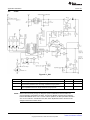
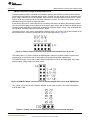
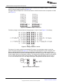
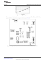
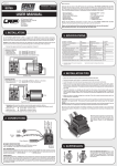
User's Guide
SNVA023B – September 2000 – Revised May 2013
AN-1164 LM3647 Reference Design Demonstration Board
1
General Description
The LM3647 is a charge controller for Nickel-Cadmium (Ni-Cd), Nickel-Metal Hydride (Ni-MH) or LithiumIon (Li-Ion) batteries. The device uses a pulsed-current charging or a constant-current charging technique.
The device can also be configured to discharge before charging. Throughout the charging sequence the
LM3647 monitors voltage and/or temperature and time in order to terminate charging.
• Negative delta voltage (−ΔV)
• Maximum voltage
• Optional: Delta temperature/delta time (ΔT/Δt)
• Optional: Maximum temperature
• Backup: Maximum time
The LM3647 is user configurable for three battery chemistries: Ni-Cd, Ni-MH or Li-Ion.
2
In
•
•
•
•
Ni-Cd/Ni-MH mode, four different charging phases are used:
Softstart charge
Fast charge
Topping charge
Maintenance charge
In
•
•
•
•
Li-Ion mode, four different charging stages are used:
Qualification
Fast Charge Phase 1, Constant Current
Fast Charge phase 2, Constant Voltage
Maintenance charge
Key Features
•
•
•
•
•
•
•
•
•
Auto-adaptive fast charge
High-resolution, accurate voltage monitoring prevents Li-Ion under-charge or overcharge
Fast charge, pre-charge and maintenance currents are provided. Different currents are selectable via
external resistors
Fast-charge termination by temperature/time, maximum voltage, maximum temperature and maximum
time
Dynamically detects battery insertion, removal, short circuit and bad battery without additional
hardware
Supports charging of battery packs with 2-8 cells of Ni-Cd, Ni-MH or 1-4 cells of Li-Ion
Three LED indicators and one Buzzer output indicate operational modes
Ni-MH/Ni-Cd charge mode, Li-Ion charge mode or discharge mode can be selected manually
PWM switching controller
SNVA023B – September 2000 – Revised May 2013
Submit Documentation Feedback
AN-1164 LM3647 Reference Design Demonstration Board
Copyright © 2000–2013, Texas Instruments Incorporated
1
Documentation Information
3
www.ti.com
Documentation Information
The following documentation describes how to use the LM3647 demo board and also gives a few tips on
design calculations. Not all components on the demo board are used when designing a charger
application. The demo board has extra components to make it simple for the user to try out different
batteries and configurations. There are actually two different charge current regulation methods and these
are referred to as fast and slow (LM317).
4
Jumper Settings
J5
Type Select
VCC
Ni-MH
GND
Ni-Cd
Hi-Z
Li-Ion
J2
Charge Mode
VCC
No discharge
GND
Maintenance charge only
Hi-Z
Discharge before charge
J2
4.1
Maintenance Mode
VCC
Charge indefinitely
GND
No charge and restart fast-charge if battery becomes discharged
Hi-Z
Charge indefinitely and restart fast-charge if battery becomes discharged
J5
J6
J7
Regulation Method / Cell Voltage
VCC
VCC
GND
Fast
Slow
LM3647 controls charge current
External (LM317) charge control
GND
VCC
GND
Fast
Slow
LM3647 controls charge current
External (LM317) charge control
Hi-Z
VCC
GND
Fast
Fast
4.2V/Cell Li-Ion
4.1V/Cell Li-Ion
Timeout
Timeout settings J18 (set according to charge-rate C).
4.2
Temperature Input
The optional Temperature input is connected to J3 and if not used Short J8.
4.3
Voltage Regulation Range
Voltage regulation loop setting J14 (not used with external LM317 regulation; J7 = slow), defines
maximum voltage output. See also Section 7.
4.4
Voltage Measurement
The battery voltage is selected with the voltage jumpers J11 and J12 depending on number of
cells/chemistry (see Figure 1). For instance, a 9V Ni-Cd block battery has 6 cells in it and therefore needs
the jumper at "Ni 6-Cells" on J11 and J12:
2
AN-1164 LM3647 Reference Design Demonstration Board
SNVA023B – September 2000 – Revised May 2013
Submit Documentation Feedback
Copyright © 2000–2013, Texas Instruments Incorporated
Jumper Settings
www.ti.com
Figure 1. Voltage Measurement
4.5
Charge Current
The charge settings for LM3647 current control are shown below. If the external LM317 is used to control
the charge current then the jumpers J9, J10 and J13 have no relevance, when using LM317 regulation
mode, this jumper must be placed in either position. If external (LM317) regulation is used then set jumper
J7 to position "slow"; for LM3647 regulation set J7 to "fast".
4.6
LM3647 Current Regulation
The I jumper J10 is used to select between different current sense resistors. The values available are
0.047Ω and 0.100Ω (see Figure 2).
Figure 2. Jumper J10 Selects Between Current Sense Resistors
The charge current is set with jumpers J9 and J13. Figure 3 shows two possible currents that depend on
how jumper J10 is set. The higher current is selected when J10 is set to 0.047Ω and the lower current is
selected when J10 is set to 0.100Ω.
Figure 3. Charge Current is Set with Jumpers J9 and J13
SNVA023B – September 2000 – Revised May 2013
Submit Documentation Feedback
AN-1164 LM3647 Reference Design Demonstration Board
Copyright © 2000–2013, Texas Instruments Incorporated
3
Functional Description
5
5.1
www.ti.com
Functional Description
General
The LM3647 has voltage and current sensing inputs that are used to control a PWM-output. The voltage
input is connected to the battery via a resistor divider network, and the current input is connected to an
operational amplifier that amplifies the voltage across a current sense resistor located at the positive
battery terminal. The PWM-output can be configured as a high-speed PWM, or as a low-speed (ON/OFF)
output for an external current regulator. The latter is for low-cost Ni-Cd/Ni-MH charger applications,
eliminating the need for any operational amplifiers or current feedback circuitry.
The high-speed PWM is filtered to a DC-level and fed into an operational amplifier that controls a powerNPN transistor. The LM3467 requires charge current feedback to control the charge current.
5.2
5.2.1
Modes of Operation
Charging Ni-Cd/Ni-MH Batteries
The charger detects that a battery is connected when the CEL-pin > 1.0V. The charger can also detect a
battery that has been deeply discharged and does not have any voltage across the battery terminals. This
is accomplished by applying a small "pre-charge' current once every minute for up to 15 seconds. The
deeply discharged battery will accept this charge and the battery potential will eventually rise above the
1.0V limit to initiate normal charging. When the charger has detected a battery (CEL-pin > 1.0V), it checks
to see if the temperature is within range to start charging. If it is, then it applies a small current of 0.2C for
approximately 5 minutes. If the battery voltage exceeds the maximum battery voltage (CEL-pin > 3.017V),
the LM3647 stops charging and stays in error mode until the battery is removed. If the battery voltage has
not risen above the bad battery threshold (CEL-pin < 1.2V), then the battery is considered to be defective
and the charger goes into error mode. If the battery passes all tests, then after the five minutes have
passed, the charger starts the next phase: Fast Charge.
During Fast Charge, the charger applies a constant current to the battery and monitors both battery
voltage and temperature. The charger is looking for a drop in the battery voltage that normally occurs at
the end of the Fast Charge cycle. The size of the voltage drop differs depending on battery type (Ni-Cd/NiMH). For Ni-Cd it is approximately 50 mV/cell and for Ni-MH it is approximately 17 mV/cell. If the
temperature rise is larger than 50 mV/minute (∼1°C/minute) when charging Ni-MH batteries, the battery
has reached the end of the Fast Charge cycle.
During charging the temperature-input is constantly measured to ensure that the battery's temperature is
within proper range. If the temperature is out of range, the charger aborts the charge and goes into error
mode.
During the next charge phase (Topping Charge) the LM3647 applies a small current of 0.2C for a time set
by the time-selection RC-network. This phase may be followed by a Maintenance Charge phase,
depending on selection-pins.
5.2.2
Charging Li-Ion Batteries
The charger detects that a battery is connected when the CEL-pin > 1.0V. The charger can also detect a
battery that has been deeply discharged and does not have any voltage across the battery terminals. This
is accomplished by applying a small "pre-charge" current once every minute for up to 15 seconds. The
deeply discharged battery will accept this charge and the battery potential will eventually rise above the
1.0V limit to initiate normal charging. When the charger has detected a battery (CEL-pin > 1.0V), it checks
to see if the temperature is within range to start charging. If it is, then it applies a small current of 0.2C for
approximately 1 minute. If the battery voltage is close to fully charged, the charger will not reach the
charging voltage within 1 minute, and the charge process will restart. This occurs only with batteries that
are already fully charged, and consequently should not be recharged. If the battery voltage has not
reached the Li-Ion battery qualification voltage (CEL-pin > 1.2V) within 1 minute of the Qualification
Phase, the battery is considered to be defective, and the charger goes into error mode. It stays there until
the battery is removed (CEL-pin < 1.0V).
4
AN-1164 LM3647 Reference Design Demonstration Board
SNVA023B – September 2000 – Revised May 2013
Submit Documentation Feedback
Copyright © 2000–2013, Texas Instruments Incorporated
Functional Description
www.ti.com
The next phase is Fast Charge Constant Current. During this phase the current is constant, and the
battery voltage will slowly rise (due to the charging). When the battery has reached its maximum battery
voltage (CEL at 2.675V or 2.74V, depending on SEL3, it will go to the next phase which is Fast Charge
Constant Voltage.
During this phase, the charger will keep the voltage constant and stay in this phase until the current has
decreased to a threshold value (CS at 2.3V).
The battery is now fully charged, and the charger can behave in different modes, depending on SEL1. It
can either maintenance charge the battery and restart the charge process if the battery voltage drops
below the maintenance restart threshold value (CEL < 2.153V), or just maintenance charge the battery
and don't restart the charge process if the battery becomes discharged. The last mode is no maintenance
charge, and restarts the charge process if the battery voltage drops below the maintenance restart
threshold value (CEL < 2.153V).
5.2.3
•
•
•
•
•
•
5.2.4
Components Critical to Total Charger Performance
The capacitance C2 connected to CEXT must be of a type that has low internal resistance, low loss,
high stability and low dielectric absorption. The capacitance mounted on the demo board is a
metallized polyester type from WIMA, 2220 series.
The operational amplifiers U1 and U2 must be capable of rail-to-rail output, and have a high PSRR
(Power Supply Rejection Ratio), because they are both powered directly from the unregulated DCinput. U1 must also have enough current drive to control the transistor Q3. U2 should preferably have
a low input offset, since this error will be amplified.
The regulator IC2 criteria is that it has to be able to handle the input DC-voltage, and deliver enough
current to drive the circuitry (all LED's, buzzer, LM3647).
The transistor Q3 must be able to handle the charge current and (depending on charge current) must
be provided with an adequate heatsink.
The transistor Q2 must be able to handle the maximum discharge current.
The Diode D1 must be able to handle the maximum charge current.
Clarifications Regarding Circuit Schematics
The circuitry with Q4, R26 and R27 is used to protect the battery from excessive charge current. When the
current flows through the current sense resistor R9, and is amplified by U2, the voltage at U2's output
drops from 2.5V until Q4 starts conducting. It discharges the RC-network that generates the DC-voltage
from the PWM-output of the LM3647.
5.2.5
Setting The Charge Timeout
The LM3647 uses the charge timeout value as a backup termination method if the normal termination
methods fail. The charge timeout also controls the length of some of the phases like the Topping Charge
phase (Ni-Cd/Ni-MH). The timeout is selectable from a charge rate of 3.2C to 0.4C. Table 1 shows which
values will result in a certain timeout.
Table 1. Charge Timeouts
R Value
C Value
Ni-Cd/Ni-MH
Fast Charge
(minutes)
Ni-Cd/Ni-MH
Topping (minutes)
Li-lon CC
(minutes)
Li-lon CV
(minutes)
Appropriate
Charge Rates
100 kΩ
0 nF
75
20
50
75
3.2C
100 kΩ
10 nF
100
25
70
100
2.4C
100 kΩ
15 nF
160
40
110
160
1.4C
100 kΩ
22 nF
190
50
130
190
1.2C
100 kΩ
33 nF
260
65
170
260
0.9C
100 kΩ
47 nF
330
80
220
330
0.7C
100 kΩ
68 nF
450
115
300
450
0.5C
100 kΩ
100 nF
540
135
360
540
0.4C
SNVA023B – September 2000 – Revised May 2013
Submit Documentation Feedback
AN-1164 LM3647 Reference Design Demonstration Board
Copyright © 2000–2013, Texas Instruments Incorporated
5
Functional Description
www.ti.com
EXAMPLE 1:
The actual timeouts (with RCIN @ 2.5 MHz) is:
Phase
Timeout
Fast Charge
∼ 330 Minutes
Topping Charge
∼ 80 Minutes
EXAMPLE 2:
The actual timeouts (with RCIN @ 2.5 MHz) is:
Phase
5.2.6
Timeout
Fast Charge Constant Current
− 130 Minutes
Topping Charge Constant Voltage
− 190 Minutes
Setting The Charge Current
The charge-current is selected by setting the current sensing resistor and the gain of the differential
amplification stage. The current sensing resistor (R5) should be dimensioned such that the voltage drop
over it is not too small, since the signal will be more susceptible to noise and offsets in the amplificationstage. The resistance should not be too large either (especially in high-current applications), because this
will only generate more heat from the component. A suitable value is one where 50 mV dropped across
the resistor when maximum current flows through it. The differential signal is then amplified, inverted and
centered around the 2.5V reference by the operational amplifier and fed to the CS pin on the LM3647. The
gain must be dimensioned by setting the appropriate ratio between R1 (R2) and R3 (R4). Figure 4 is
dimensioned for a maximum current of about 1.1A. This was dimensioned using the following formula:
(1)
6
AN-1164 LM3647 Reference Design Demonstration Board
SNVA023B – September 2000 – Revised May 2013
Submit Documentation Feedback
Copyright © 2000–2013, Texas Instruments Incorporated
Functional Description
www.ti.com
Figure 4. Setting the Chart Current
5.2.7
Setting Maximum Battery Voltage
The resistor network (see Figure 5) scales the battery voltage to a suitable level for the LM3647. For NiCd/Ni-MH batteries the network is less critical, but limits the maximum battery voltage, it is only used as a
backup termination method. For Li-Ion batteries the network must be more accurate, requiring precision
resistors with low tolerances.
• For Ni-Cd/Ni-MH:
The dimensioning is accomplished in the following manner:
First calculate the maximum battery voltage for the specific battery pack. See the example below.
BatteryVoltage/Cell = 1.2V NumberOfCells = 5 → BatteryPackVoltage = 1.2×5 = 6V
MaximumBatteryVoltage/Cell = 1.85V → MaximumBatteryVoltage = 1.85×5 = 9.25V
(2)
(3)
When the Maximum Battery Voltage has been determined, the voltage divider network has to be
dimensioned using the following formula:
Figure 5. Maximum Battery Voltage
•
For Li-Ion:
SNVA023B – September 2000 – Revised May 2013
Submit Documentation Feedback
AN-1164 LM3647 Reference Design Demonstration Board
Copyright © 2000–2013, Texas Instruments Incorporated
7
Functional Description
www.ti.com
The voltage divider network for Li-Ion is very important. If the battery voltage is scaled too low, the battery
will not attain its full capacity when charged, and if scaled too high, the battery may become damaged.
Never exceed the recommended maximum voltage or current for a Li-Ion battery!
The dimensioning is done in the following manner.
First calculate the maximum battery voltage for the specific battery pack. See example below.
BatteryVoltage/Cell = 3.6V NumberOfCells = 2 → BatteryPackVoltage = 3.6×2 = 7.2V
MaximumBatteryVoltage/Cell = 4.1V → MaximumBatteryVoltage = 4.1×2 = 8.2V
(4)
(5)
When the maximum battery voltage has been determined, the voltage divider network has to be
dimensioned using the following formula:
(6)
The LM3647 has two different regulation voltages, which the user can select: the 2.675V (SEL3 tied to
GND) and 2.740V (SEL3 tied to VCC). This selection pin can be used to configure the charger to regulate
for different input voltages so that the charger can handle both 3.6V- and 3.7V-cells, without changing the
resistor values in the divider network. SEL3 can also be used if there is problem in finding the right values
in the resistor network. The recommended tolerance of the resistors are 0.1%, but 1% may be used with a
marginal loss of battery capacity by subtracting the tolerance of the divider network from the maximum
battery voltage.
• Using the LM3647 without current feedback, for Ni-Cd/Ni-MH only (slow PWM mode):
This mode uses an external constant-current power-source, which is switched on and off according to the
charge-phase of the LM3647. The frequency is approximately 0.1 Hz. The advantage of this charge
method is that operational amplifiers and the current feedback circuitry are not needed, which provides a
low-cost solution. The dimensioning of the voltage divider network is performed the same way. The
constant current source is dimensioned in the following manner:
(7)
Figure 6. LM3647 Regulator
The LM3647 regulates the constant current source by turning the transistor Q1 on and of (see Figure 6).
When the transistor is off, the LM317T regulator feeds a constant current to the battery (at V_OUT).
When the transistor is on, the output from the LM317 is limited to 1.25V (which should be greater than the
battery voltage).
Charge Phase:
8
Duty Cycle:
Soft Start
10%
Fast Charge
100%
Topping Charge
10%
Maintenance Charge
5%
AN-1164 LM3647 Reference Design Demonstration Board
SNVA023B – September 2000 – Revised May 2013
Submit Documentation Feedback
Copyright © 2000–2013, Texas Instruments Incorporated
Application information
www.ti.com
6
6.1
Application information
Typical Example
6.1.1
Ni-Cd/Ni-MH
Figure 7.
Set To:
Ni-Cd/Ni-MH
SEL1
SEL2
SEL3
VCC
No Discharge before Charge
Ni-MH
Fast-PWM (LM3647 has current feedback)
Hi-Z
Discharge before Charge
NA
NA
GND
Maintenance Charge Only
Ni-Cd
Slow-PWM (external current control)
SNVA023B – September 2000 – Revised May 2013
Submit Documentation Feedback
AN-1164 LM3647 Reference Design Demonstration Board
Copyright © 2000–2013, Texas Instruments Incorporated
9
Application information
6.2
www.ti.com
Li-Ion
Figure 8. Li_ION
Set To:
SEL1
SEL2
SEL3
VCC
After charging, maintenance charging until battery removal.
NA
4.2V/Cell
Hi-Z
After charging, maintenance charging until battery removal. If battery voltage
drops below a predefined value, the charger restarts the charge-process.
Li-Ion
NA
GND
After charging, no maintenance charging is applied. If battery voltage drops
below a predefined value, the charger restarts the charge-process.
NA
4.1V/Cell
NOTE: When a three chemistry charger is designed, special considerations must be taken into
account regarding configuration pin SEL3. This pin has different meanings when switching
between Ni-Cd/Ni-MH and Li-Ion. To ensure correct operation, the SEL3-pin MUST be tied to
VCC. If Li-Ion cells of 4.1V/Cells are used, then minor adjustments have to be done to the
voltage measurement resistor divider.
10
AN-1164 LM3647 Reference Design Demonstration Board
SNVA023B – September 2000 – Revised May 2013
Submit Documentation Feedback
Copyright © 2000–2013, Texas Instruments Incorporated
LM3647 Reference Design Demonstration Board
www.ti.com
7
LM3647 Reference Design Demonstration Board
The demo board provides a combined multi-chemistry solution with hardware for both external constant
current source and LM3647 controlled charge current. Located near the top-left corner of the board is the
power supply connector (next to the heatsink). When using the external constant current source, a power
resistor needs to be connected at the connector marked 317-resistor. The values of the resistor can be
calculated using the Equation 4 mentioned earlier.
At the bottom-right corner of the board are two connectors that lead to the battery and discharge resistor.
The value of the discharge resistor depends on the battery pack voltage and the maximum discharge rate.
The demo board has different jumpers that are assigned to different setups. Some of the components are
not populated, providing support for user-specific values.
The timeout jumper J18 is used to select different timeouts from 2.4C to 0.4C. The values mounted on the
demo board result in timeouts corresponding to the charge-rates shown in Figure 9.
Figure 9. Timeout Jumper J18 Used to Select Different Timeouts From 2.4C to 0.4C
The PWM jumper J7 is used to connect the PWM-signal to either the external constant current source
(marked slow) or the RC-filter that is connected to the operational amplifier (marked fast).
The PWM-FB jumper J14 is used to select different amplification levels of the PWM signal. The jumper
with the battery voltage ranges are shown below:
Figure 10. PWM-FB Jumper J14 Used to Select Different Amplification Levels of the PWM Signal
The I jumper J10 is used to select between different current sense resistors. The values mounted are
0.047Ω and 0.100Ω.
Figure 11. Jumper J10 Used to Select Between Different Current Sense Resistors
SNVA023B – September 2000 – Revised May 2013
Submit Documentation Feedback
AN-1164 LM3647 Reference Design Demonstration Board
Copyright © 2000–2013, Texas Instruments Incorporated
11
LM3647 Reference Design Demonstration Board
www.ti.com
The different current sense voltage amplification level is selected via CURRENT jumpers J9 and J13 (both
jumpers must be changed in pairs, see Figure 12).
The upper values correspond to a current sense resistor of 0.047Ω while the lower correspond to 0.100Ω
(see Figure 11).
Figure 12. CURRENT Jumpers J9 and J13
The battery voltage is selected with the Voltage jumpers J11 and J12 (see Figure 13 for settings).
Figure 13. Voltage Jumpers 11 and 12
The jumper J3 is used to connect to an optional NTC-resistor. If no temperature sensor is used, the
jumper J8 must be shorted (see Figure 14) . The demo board was designed for an NTC thermistor from
Siemens (B57861S302F40) with the following specifications: 3kΩ @ 25°C, β = 3988. If an NTC with
different characteristics is used, then the resistor R28 may need to be changed. The charger uses voltage
levels to trigger under/over temperature conditions. The voltage at the temperature-input must be between
2.2V or 0.5V for the charger to start. During charging the voltage must stay between 3.0V for Li-Ion, or
3.15V for Ni-Cd/Ni-MH, and 0.5V or the charger will register a temperature fault and abort the charge.
Figure 14. Jumper J3 or Jumper 8
12
AN-1164 LM3647 Reference Design Demonstration Board
SNVA023B – September 2000 – Revised May 2013
Submit Documentation Feedback
Copyright © 2000–2013, Texas Instruments Incorporated
LM3647 Reference Design Demonstration Board
www.ti.com
Figure 15. Voltage Temperature
The three jumpers J2, J5, and J6 are connected to the three selection-pins SEL1, SEL2, and SEL3. These
jumpers are used to select how the charger should behave (see Table 1).
Figure 16. Jumpers J2, J5, and J6 Connected to 3 Selection Pins SEL1, SEL2, and SEL3
SNVA023B – September 2000 – Revised May 2013
Submit Documentation Feedback
AN-1164 LM3647 Reference Design Demonstration Board
Copyright © 2000–2013, Texas Instruments Incorporated
13
IMPORTANT NOTICE
Texas Instruments Incorporated and its subsidiaries (TI) reserve the right to make corrections, enhancements, improvements and other
changes to its semiconductor products and services per JESD46, latest issue, and to discontinue any product or service per JESD48, latest
issue. Buyers should obtain the latest relevant information before placing orders and should verify that such information is current and
complete. All semiconductor products (also referred to herein as “components”) are sold subject to TI’s terms and conditions of sale
supplied at the time of order acknowledgment.
TI warrants performance of its components to the specifications applicable at the time of sale, in accordance with the warranty in TI’s terms
and conditions of sale of semiconductor products. Testing and other quality control techniques are used to the extent TI deems necessary
to support this warranty. Except where mandated by applicable law, testing of all parameters of each component is not necessarily
performed.
TI assumes no liability for applications assistance or the design of Buyers’ products. Buyers are responsible for their products and
applications using TI components. To minimize the risks associated with Buyers’ products and applications, Buyers should provide
adequate design and operating safeguards.
TI does not warrant or represent that any license, either express or implied, is granted under any patent right, copyright, mask work right, or
other intellectual property right relating to any combination, machine, or process in which TI components or services are used. Information
published by TI regarding third-party products or services does not constitute a license to use such products or services or a warranty or
endorsement thereof. Use of such information may require a license from a third party under the patents or other intellectual property of the
third party, or a license from TI under the patents or other intellectual property of TI.
Reproduction of significant portions of TI information in TI data books or data sheets is permissible only if reproduction is without alteration
and is accompanied by all associated warranties, conditions, limitations, and notices. TI is not responsible or liable for such altered
documentation. Information of third parties may be subject to additional restrictions.
Resale of TI components or services with statements different from or beyond the parameters stated by TI for that component or service
voids all express and any implied warranties for the associated TI component or service and is an unfair and deceptive business practice.
TI is not responsible or liable for any such statements.
Buyer acknowledges and agrees that it is solely responsible for compliance with all legal, regulatory and safety-related requirements
concerning its products, and any use of TI components in its applications, notwithstanding any applications-related information or support
that may be provided by TI. Buyer represents and agrees that it has all the necessary expertise to create and implement safeguards which
anticipate dangerous consequences of failures, monitor failures and their consequences, lessen the likelihood of failures that might cause
harm and take appropriate remedial actions. Buyer will fully indemnify TI and its representatives against any damages arising out of the use
of any TI components in safety-critical applications.
In some cases, TI components may be promoted specifically to facilitate safety-related applications. With such components, TI’s goal is to
help enable customers to design and create their own end-product solutions that meet applicable functional safety standards and
requirements. Nonetheless, such components are subject to these terms.
No TI components are authorized for use in FDA Class III (or similar life-critical medical equipment) unless authorized officers of the parties
have executed a special agreement specifically governing such use.
Only those TI components which TI has specifically designated as military grade or “enhanced plastic” are designed and intended for use in
military/aerospace applications or environments. Buyer acknowledges and agrees that any military or aerospace use of TI components
which have not been so designated is solely at the Buyer's risk, and that Buyer is solely responsible for compliance with all legal and
regulatory requirements in connection with such use.
TI has specifically designated certain components as meeting ISO/TS16949 requirements, mainly for automotive use. In any case of use of
non-designated products, TI will not be responsible for any failure to meet ISO/TS16949.
Products
Applications
Audio
www.ti.com/audio
Automotive and Transportation
www.ti.com/automotive
Amplifiers
amplifier.ti.com
Communications and Telecom
www.ti.com/communications
Data Converters
dataconverter.ti.com
Computers and Peripherals
www.ti.com/computers
DLP® Products
www.dlp.com
Consumer Electronics
www.ti.com/consumer-apps
DSP
dsp.ti.com
Energy and Lighting
www.ti.com/energy
Clocks and Timers
www.ti.com/clocks
Industrial
www.ti.com/industrial
Interface
interface.ti.com
Medical
www.ti.com/medical
Logic
logic.ti.com
Security
www.ti.com/security
Power Mgmt
power.ti.com
Space, Avionics and Defense
www.ti.com/space-avionics-defense
Microcontrollers
microcontroller.ti.com
Video and Imaging
www.ti.com/video
RFID
www.ti-rfid.com
OMAP Applications Processors
www.ti.com/omap
TI E2E Community
e2e.ti.com
Wireless Connectivity
www.ti.com/wirelessconnectivity
Mailing Address: Texas Instruments, Post Office Box 655303, Dallas, Texas 75265
Copyright © 2013, Texas Instruments Incorporated