1
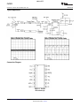
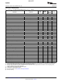
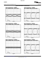
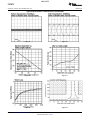
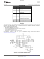
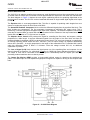
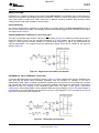
OBSOLETE
CLC012
www.ti.com
SNLS032E – AUGUST 1998 – REVISED APRIL 2013
CLC012 Adaptive Cable Equalizer for ITU-T G.703 Data Recovery
Check for Samples: CLC012
FEATURES
DESCRIPTION
•
TI's CLC012 adaptive cable equalizer is a low-cost
monolithic solution for equalizing data transmitted
over cable (or any media with similar dispersive loss
characteristics). The CLC012 simplifies the task of
high-speed data recovery with a one-chip solution
and a minimal number of external components. The
equalizer automatically adapts to equalize any cable
length from zero meters to lengths that attenuate the
signal by 40 dB at 200 MHz. This corresponds to 300
meters of Belden 8281 or 120 meters of Category 5
UTP (unshielded twisted pair).
1
23
•
•
•
•
•
Automatic Equalization of Coaxial and Twisted
Pair Cables
Loss of Signal Detect and Output Mute
Output Eye Monitor
Single Supply Operation: +5V or −5.2V
Single-Ended or Differential Input
Low Cost
APPLICATIONS
•
•
•
•
ITU-T G.703 Serial Data Recovery
Serial Digital Data Routing and Distribution
Serial Digital Data Equalization and Reception
Data Recovery Equalization: ATM, CAD
Networks, Medical, Set Top Terminals,
Industrial Video Networks
KEY SPECIFICATIONS
•
•
•
•
•
Low Jitter: 180pspp @ 270 Mbps Through 200
Meters of Belden 8281 Coaxial Cable
High Data Rates: < 50 Mbps to > 650 Mbps
Excellent Input Return Loss: 19 dB @ 270 MHz
Low Supply Current: 68 mA
Equalizes up to 300+ Meters of Belden 8281 or
120 Meters of Cat 5 UTP Cable
The CLC012 provides superior jitter performance:
180pspp for 270 Mbps data that has passed through
200 meters of Belden 8281 cable. This exceptional
performance provides wide error margin in digital
data links. The equalizer operates on a single supply
with a power consumption of only 290 mW. The small
14-pin SOIC package allows for high-density
placement of components for multi-channel
applications such as routers. The equalizer operates
over a wide range of data rates from less than 50
Mbps to rates in excess of 650 Mbps.
The equalizer is flexible in allowing either singleended or differential input drive. Its high common
mode rejection provides excellent immunity to
interference from noise sources. On-chip quantized
feedback eliminates baseline wander.
Additional features include a Loss of Signal output
and an output mute pin which, when tied together,
mute the output when no signal is present. A buffered
eye monitor output is provided, for viewing the
equalized signal prior to the comparator. Differential
AEC pins allow the user to set the internal adaptive
loop time constant with one external capacitor.
1
2
3
Please be aware that an important notice concerning availability, standard warranty, and use in critical applications of
Texas Instruments semiconductor products and disclaimers thereto appears at the end of this data sheet.
WEBENCH is a registered trademark of Texas Instruments.
All other trademarks are the property of their respective owners.
PRODUCTION DATA information is current as of publication date.
Products conform to specifications per the terms of the Texas
Instruments standard warranty. Production processing does not
necessarily include testing of all parameters.
Copyright © 1998–2013, Texas Instruments Incorporated
OBSOLETE
CLC012
SNLS032E – AUGUST 1998 – REVISED APRIL 2013
www.ti.com
Typical Application
Connection Diagram
Figure 1. Pinout
14-Pin SOIC (D)
2
Submit Documentation Feedback
Copyright © 1998–2013, Texas Instruments Incorporated
Product Folder Links: CLC012
OBSOLETE
CLC012
www.ti.com
SNLS032E – AUGUST 1998 – REVISED APRIL 2013
These devices have limited built-in ESD protection. The leads should be shorted together or the device placed in conductive foam
during storage or handling to prevent electrostatic damage to the MOS gates.
Absolute Maximum Ratings (1) (2)
−0.3V, +6.5V
Supply Voltage (VCC–VEE)
Maximum Junction Temperature
+150°C
−65°C to +150°C
Storage Temperature Range
Lead Temperature (Soldering 4 sec.)
+260°C
ESD Rating (3)
≥500V
θJA 14-Pin SOIC (AJE)
95°C/W
4.8 x 10⁷ hours
MTTF (based on limited life test data)
(1)
(2)
(3)
“Absolute Maximum Ratings” are those values beyond which the safety of the device cannot be ensured. They are not meant to imply
that the devices should be operated at these limits. The table of “Electrical Characteristics” specifies conditions of device operation.
If Military/Aerospace specified devices are required, please contact the Texas Instruments Sales Office/Distributors for availability and
specifications.
Human body model, 1.5 kΩ in series with 100 pF; based on limited test data.
Recommended Operating Conditions
Supply Voltage (VCC–VEE)
4.5V to 5.5V
−40°C to +85°C
Operating Temperature Range
Series Input Resistance (In Series w/DI & DI)
100Ω
1.0 μF
Input Coupling Capacitance
50 pF to 1 μF
AEC Capacitor (Connected between AEC+ & AEC−)
Cable Input Voltage Swing (1)
DO/DO Minimum Voltage
(1)
(2)
720 to 880 mVpp
(2)
VCC–1.6V
These specifications assume an 800 mVpp signal at the cable input. Levels above and below 800 mV are allowable, but performance
may vary. The cable will attenuate the signal prior to entering the equalizer.
To maintain specified performance, do not reduce DO/DO below this level.
Submit Documentation Feedback
Copyright © 1998–2013, Texas Instruments Incorporated
Product Folder Links: CLC012
3
OBSOLETE
CLC012
SNLS032E – AUGUST 1998 – REVISED APRIL 2013
www.ti.com
Electrical Characteristics
(VCC = +5V, VEE = 0V, signal source swing = 0.8 Vpp (1), CAEC = 100 pF)
Parameter
Conditions
Typ
+25°C
Min/Max
+25°C (2)
Min/Max
−40°C to
+85°C (2)
Units
DYNAMIC PERFORMANCE
Residual Jitter
10 meters Belden 8281
311 Mbps PRN (3)
150
250
400
pspp
300 meters Belden 8281
311 Mbps PRN (3) (4)
350
500
750
pspp
100 meters Belden 8281
CAEC = 100 pF (5)
1.5
_
_
μs
200 meters Belden 8281
CAEC = 100 pF (5)
2.0
_
_
μs
300 meters Belden 8281
CAEC = 100 pF (5)
3.2
_
_
μs
Rcollector = 75Ω
750
_
_
ps
Equalization Time Constant
output rise and fall time (20%–80%)
output duty cycle distortion
30
_
_
ps
1/50
_
_
trans/ns
650
_
_
Mbps
27 MHz
0.85
_
_
ns/V
270 MHz
1.90
_
_
ns/V
27 MHz
0.55
_
_
ns/V
270 MHz
1.45
_
_
ns/V
minimum average transition density
maximum average data rate
150m Belden 8281 (6)
VCC Jitter Sensitivity
VEE Jitter Sensitivity
STATIC PERFORMANCE
Supply Current (Includes Output Current)
VAEC = 0V
See (4)
68
48/75
40/80
mA
VAEC = 0.4V
See (4)
53
43/64
37/70
mA
10
8.7/11.3
8.0/12
mA
Rcollector = 75Ω (4)
750
650/850
600/900
mV
3.4
_
_
V
1.5
_
_
mV/meter
AEC+/AEC− common mode
3.6
_
_
V
output eye monitor (OEM) bias potential
3.2
_
_
V
Input and Output Parameters
DO/DO output current
DO/DO output voltage swing
DI/DI common mode voltage
AEC differential voltage
Belden 8281
Loss of Signal (LOS) current output-HIGH
LOS VOH = 4.5V
−400
_
_
μA
Loss of Signal (LOS) current output-LOW
LOS VOL = 0.5V
600
_
_
μA
MUTE voltage input-HIGH
See (4)
1.8
2.0
2.0
V
MUTE voltage input-LOW
See
(4)
1.2
0.8
0.8
V
MUTE current input-HIGH
VIH = 5V (4)
5.0
±100
±500
nA
MUTE current input-LOW
VIL = 0V (4)
0.2
±100
±500
nA
(1)
(2)
(3)
(4)
(5)
(6)
4
These specifications assume an 800 mVpp signal at the cable input. Levels above and below 800 mV are allowable, but performance
may vary. The cable will attenuate the signal prior to entering the equalizer.
Min/max ratings are based on product characterization and simulation. Individual parameters are tested as noted. Outgoing quality
levels are determined from tested parameters.
Peak-to-peak jitter is defined as 6 times the rms jitter.
J-level: spec. is 100% tested at +25°C.
For more information, see Operation and Design Guidelines.
50% eye opening.
Submit Documentation Feedback
Copyright © 1998–2013, Texas Instruments Incorporated
Product Folder Links: CLC012
OBSOLETE
CLC012
www.ti.com
SNLS032E – AUGUST 1998 – REVISED APRIL 2013
Electrical Characteristics (continued)
(VCC = +5V, VEE = 0V, signal source swing = 0.8 Vpp(1), CAEC = 100 pF)
Parameter
Conditions
Typ
+25°C
Min/Max
+25°C (2)
Min/Max
−40°C to
+85°C (2)
Units
TIMING PERFORMANCE
LOS Response Time
carrier applied
See (7)
150
1000
1000
ns
carrier removed
See (8)
150
1000
1000
ns
MUTE response time
See (9)
2.0
_
_
ns
input resistance
single-ended
7.3
_
_
kΩ
input capacitance
single-ended (10)
1.0
_
_
pF
input return loss @ 270 MHz
Zo = 75Ω (11)
19
_
_
dB
maximum cable attenuation
200 MHz (12)
40
_
_
dB
MISCELLANEOUS PERFORMANCE
(7)
(8)
(9)
(10)
(11)
(12)
Time from application of a valid signal to when the LOS output asserts high.
Time from the removal of a valid signal to when the LOS output asserts low.
Time from assertion of MUTE to when the output responds.
Device only. Does not include typical pc board parasitics.
Includes typical pc board parasitics.
This sets the maximum cable length for the equalizer.
Submit Documentation Feedback
Copyright © 1998–2013, Texas Instruments Incorporated
Product Folder Links: CLC012
5
OBSOLETE
CLC012
SNLS032E – AUGUST 1998 – REVISED APRIL 2013
www.ti.com
Typical Performance Characteristics
6
Figure 2.
Figure 3.
Figure 4.
Figure 5.
Figure 6.
Figure 7.
Submit Documentation Feedback
Copyright © 1998–2013, Texas Instruments Incorporated
Product Folder Links: CLC012
OBSOLETE
CLC012
www.ti.com
SNLS032E – AUGUST 1998 – REVISED APRIL 2013
Typical Performance Characteristics (continued)
Figure 8.
Figure 9.
Figure 10.
Figure 11.
Figure 12.
Figure 13.
Submit Documentation Feedback
Copyright © 1998–2013, Texas Instruments Incorporated
Product Folder Links: CLC012
7
OBSOLETE
CLC012
SNLS032E – AUGUST 1998 – REVISED APRIL 2013
www.ti.com
Typical Performance Characteristics (continued)
8
Figure 14.
Figure 15.
Figure 16.
Figure 17.
Figure 18.
Figure 19.
Submit Documentation Feedback
Copyright © 1998–2013, Texas Instruments Incorporated
Product Folder Links: CLC012
OBSOLETE
CLC012
www.ti.com
SNLS032E – AUGUST 1998 – REVISED APRIL 2013
PIN DEFINITIONS
Name
DI, DI
DO, DO
AEC+, AEC−
Pin #
8, 9
13, 14
6, 7
Description
Differential data inputs.
Differential collector data outputs (ECL
compatible).
AEC loop filter pins.
A capacitor connected between these pins
governs the loop response for the adaptive
equalization loop.
OEM
3
Eye monitor output. The output of the
equalization filter.
LOS
5
Loss of Signal. (Low when no signal is
present).
MUTE
12
Output MUTE. (Active low.)
Loss of Signal (LOS) may be tied to this pin
to inhibit the output when no signal is
present.
VCC
1, 2, 4
Positive supply pins (ground or +5V).
VEE
10, 11
Negative supply pins (−5.2V or ground).
Operation
The CLC012 Adaptive Cable Equalizer provides a complete solution for equalizing high-bit-rate digital data
transmitted over long transmission lines. The following sections furnish design and application information to
assist in completing a successful design:
• Block diagram explanation of the CLC012
• Recommended standard input and output interface connections
• Common applications for the CLC012
• Measurement, PC layout, and cable emulation boxes
For applications assistance in the U.S., go to the WEBENCH® Design Center Team's website at
www.ti.com/ww/en/analog/webench/.
Figure 20. CLC012 Equalizer Application Circuit
Submit Documentation Feedback
Copyright © 1998–2013, Texas Instruments Incorporated
Product Folder Links: CLC012
9
OBSOLETE
CLC012
SNLS032E – AUGUST 1998 – REVISED APRIL 2013
www.ti.com
BLOCK DESCRIPTION
The CLC012 is an adaptive equalizer that reconstructs serial digital data received from transmission lines such
as coaxial cable or twisted pair. Its transfer function approximates the reciprocal of the cable loss characteristic.
The block diagram in Figure 21 depicts the main signal conditioning blocks for equalizing digital data at the
receiving end of a cable. The CLC012 receives baseband differential or single-ended digital signals at its inputs
DI and DI.
The Equalizer block is a two-stage adaptive filter. This filter is capable of equalizing cable lengths from zero
meters to lengths that require 40 dB of boost at 200 MHz.
The Quantized Feedback Comparator block receives the differential signals from the equalizer filter block. This
block includes two comparators. The first comparator incorporates a self-biasing DC restore circuit. This is
followed by a second high-speed comparator with output mute capability. The second comparator receives and
slices the DC-restored data. Its outputs DO and DO are taken from the collectors of the output transistors. MUTE
latches DO and DO when a TTL logic low level is applied.
The Adaptive Servo Control block produces the signal for controlling the filter block, and outputs a voltage
proportional to cable length. It receives differential signals from the output of the filter block and from the
quantized-feedback comparator (QFBC) to develop the control signal. The servo loop response is controlled by
an external capacitor placed across the AEC+ and AEC− pins. Its output voltage, as measured differentially
across AEC+ and AEC−, is roughly proportional to the length of the transmission line. For Belden 8281 coaxial
cable this differential voltage is about 1.5 mV/meter. Once this voltage exceeds 500 mV, no additional
equalization is provided.
The Loss of Signal (LOS) block monitors the signal power out of the equalizing filter and compares it to an
internal reference to determine if a valid signal is present. A CMOS high output indicates that data is present.
The output of LOS can be connected to the MUTE input to automatically latch the outputs (DO and DO),
preventing random transitions when no data is present.
The Output Eye Monitor (OEM) provides a single-ended buffered output for observing the equalized eye
pattern. The OEM output is a low impedance high-speed voltage driver capable of driving an AC-coupled 100Ω
load.
Figure 21. CLC012 Block Diagram
10
Submit Documentation Feedback
Copyright © 1998–2013, Texas Instruments Incorporated
Product Folder Links: CLC012
OBSOLETE
CLC012
www.ti.com
SNLS032E – AUGUST 1998 – REVISED APRIL 2013
DEVICE TESTING
Performance or compliancy testing of the CLC012 with Cable Clones is not allowed. Use of these devices is
contrary to the product's specifications and test procedures. Testing for product specifications or performance
using cable clones is invalid since cable clones have a different frequency response than the actual cable.
Testing with full length cable samples is recommended.
Input Interfacing
The CLC012 accepts either differential or single-ended input voltage specified in Static Performance section of
the Electrical Characteristics table. The following sections show several suggestions for interfaces for the inputs
and outputs of the CLC012.
SINGLE-ENDED INPUT INTERFACE: 75Ω Coaxial Cable
The input is connected single-ended to either DI or DI as shown in Figure 22. Balancing unused inputs helps to
lessen the effects of noise. Use the equivalent termination of 37.4Ω to balance the input impedance seen by
each pin. It also helps to terminate grounds at a common point. Resistors Rx and Ry are recommended for
optimum performance. The equalizer inputs are self-biasing. Signals should be AC coupled to the inputs as
shown in Figure 22.
Figure 22. Single-Ended 75Ω Cable Input Interface
DIFFERENTIAL INPUT INTERFACE: Twisted Pair
A recommended differential input interface is shown in Figure 23. Proper voltage levels must be furnished to the
input pins and the proper cable terminating impedance must be provided. For Category 5 UTP this is
approximately 100Ω. Figure 23 shows a generalized network which may be used to receive data over a twisted
pair. Resistors R1 and R2 provide the proper terminating impedance and signal level adjustment. The blocking
capacitors provide AC coupling of the attenuated signal levels. The plots in the Typical Performance
Characteristics section demonstrate various equalized data rates using Category 5 UTP at 100 meter lengths. A
full schematic of a recommended driver and receiver circuit for 100Ω Category 5 UTP is provided in the Typical
Applications section with further explanation.
Figure 23. Twisted Pair Input Interface
Submit Documentation Feedback
Copyright © 1998–2013, Texas Instruments Incorporated
Product Folder Links: CLC012
11
OBSOLETE
CLC012
SNLS032E – AUGUST 1998 – REVISED APRIL 2013
www.ti.com
Output Interfacing
The outputs DO and DO produce ECL logic levels when the recommended output termination networks are
used. The DO and DO pins are not complementary emitter coupled logic outputs. Instead, the outputs are
taken off of the collectors of the transistors. Therefore, care must be taken to meet the interface threshold levels
required by ECL families. Recommended interfaces for standard ECL families are shown in the following circuits.
DIFFERENTIAL LOAD-TERMINATED OUTPUT INTERFACE
Figure 24 shows a recommended circuit for implementing a differential output that is terminated at the load. A
diode or 75Ω resistor provides a voltage drop from the positive supply (+5V for PECL or Ground for ECL
operation) to establish proper ECL levels. The resistors terminate the cable to the characteristic impedance. The
output voltage swing is determined by the CLC012 output current (10 mA) times the termination resistor. For the
circuit in Figure 24, the nominal output voltage swing is 750 mV.
Figure 24. Differential Load Terminated Output Interface
DIFFERENTIAL SOURCE-TERMINATED OUTPUT INTERFACE
Figure 25 is similar to Figure 24 except that the termination is provided at the source. This configuration may also
be used for single-ended applications. However, the unused output must still be terminated as shown.
Figure 25. Differential Source Terminated Output Interface
12
Submit Documentation Feedback
Copyright © 1998–2013, Texas Instruments Incorporated
Product Folder Links: CLC012
OBSOLETE
CLC012
www.ti.com
SNLS032E – AUGUST 1998 – REVISED APRIL 2013
TERMINATING PHYSICALLY SEPARATED OUTPUTS
When the two outputs must be routed to physically separate locations, the circuit in Figure 25 may be applied.
Alternatively, if load termination is desired, the circuit in Figure 26 may be used. The resistive divider network
provides 75Ω termination and establishes proper ECL levels. This circuit consumes slightly more power than the
previous circuits.
Figure 26. Alternative Load Terminated Output Interface
Design Guidelines
SELECTING THE AUTOMATIC EQUALIZER CAPACITOR
The AEC capacitor sets the loop time constant τ for the equalizer's adaptive loop response time. The following
formula is used to set the loop time constant:
τ = R • CAEC • 10 −6
(1)
R is a conversion factor that is set by internal equalizer parameters and cable length. For Belden 8281 coaxial
cable, the R values are (τ = μs, CAEC in pF):
Cable Length
R Value (Ohms)
100 meters
15000
200 meters
20000
300 meters
32000
For example, a CAEC value of 100 pF results in an adaptive loop time constant of 2 μs at 200 meters of cable.
CONNECTION AND OPERATION OF LOS AND MUTE
Loss of Signal (LOS) is a CMOS output that indicates the presence of equalized data from the filter. This LOS
output can be connected to MUTE to suspend changes in the data outputs DO and DO, if no valid signal exists.
This simple configuration prevents random output transitions due to noise. For sparse transition patterns it is
recommended that a capacitor be connected to LOS as shown in Figure 20.
Add a capacitor to pin 5 to slow the response time of Loss of Signal when LOS is connected to MUTE. The
capacitor reduces sensitivity to pathological patterns. Pathological patterns are defined as sparse data
sequences with few transitions.
OUTPUT EYE MONITOR OEM CONNECTIONS
The OEM is a high-speed, buffered output for monitoring the equalized eye pattern prior to the output
comparator. Its output is designed to drive an AC-coupled 50Ω coaxial cable with a series 50Ω backmatch
resistor. The cable should be terminated with 50Ω at the oscilloscope. Figure 20 shows a schematic with a
typical connection.
Submit Documentation Feedback
Copyright © 1998–2013, Texas Instruments Incorporated
Product Folder Links: CLC012
13
OBSOLETE
CLC012
SNLS032E – AUGUST 1998 – REVISED APRIL 2013
www.ti.com
MINIMUM DATA TRANSITIONS
The CLC012 specifies a minimum transition rate. For the CLC012 this sets the minimum data rate for
transmitting data through any cable medium. The CLC012 minimum average transition density is found in the
Electrical Characteristics section of the datasheet.
POWER SUPPLY OPERATION AND THERMAL CONSIDERATIONS
The CLC012 operates from either +5V or −5.2V single supplies. Refer to Figure 20 when operating the part from
+5V. When operating with a −5.2V supply, the VEE pins should be bypassed to ground. The evaluation board and
associated literature provide for operation from either supply.
Maximum power dissipation occurs at minimum cable length. Under that condition, ICC = 58 mA.
Total power dissipated:
PT = (58 mA)(5V) = 290 mW
(2)
Power in the load:
PL = (0.7V)(11 mA) + (37.5)(11 mA)2 = 12 mW
(3)
Maximum power dissipated on the die:
PDMAX = PT–PL = 278 mW
(4)
Junction Temperature =
(θJA)(278 mW) + TA = T A + 26°C
(5)
Layout and Measurement
The printed circuit board layout for the CLC012 requires proper high-speed layout to achieve the performance
specifications found in the datasheet. The following list contains a few rules to follow:
1. Use a ground plane.
2. Decouple power pins with 0.1 μF capacitors placed ≤ 0.1” (3mm) from the power pins.
3. Design transmission strip lines from the CLC012's input and output pins to the board connectors.
4. Route outputs away from inputs.
5. Keep ground plane ≥ 0.025” (0.06mm) away from the input and output pads.
Figure 27 shows a block level measurement diagram, while Figure 34 on depicts a detailed schematic. A
pseudo-random pattern generator with low output jitter was used to provide a NRZI pattern to create the eye
diagrams shown in the Typical Performance Characteristics section.
Since most pattern generators have a 50Ω output impedance, a translation can be accomplished using a
CLC005 Cable Driver as an impedance transformer. A wide bandwidth oscilloscope is needed to observe the
high data rate eye pattern. When monitoring a single output that is terminated at both the equalizer output and
the oscilloscope, the effective output load is 37.4Ω. Consequently, the signal swing is half that observed for a
single-ended 75Ω termination.
Figure 27. Typical Measurement Block
14
Submit Documentation Feedback
Copyright © 1998–2013, Texas Instruments Incorporated
Product Folder Links: CLC012
OBSOLETE
CLC012
www.ti.com
SNLS032E – AUGUST 1998 – REVISED APRIL 2013
Troubleshooting with scope probes can affect the equalization. For high data rates, use a low capacitance
probe with less than 2 pF probe capacitance. Evaluation boards and literature are available for quick prototyping
and evaluation of the CLC012 Adaptive Cable Equalizer. The CLC012 contains CMOS devices and operators
should use grounding straps when handling the parts.
Figure 28 shows the CLC012's internal power supply routing. Bypass VCC (pin 4) by:
• Monolithic capacitor of about 0.1 μF placed less than 0.1” (3mm) from the pin
• Tantalum capacitor of about 6.8 μF for large current signal swings placed as close as convenient to the
CLC012
Figure 28. Power Package Routing Fixture
To minimize ringing at the CLC012's inputs, place a 100Ω resistor in series with the input. This resistor reduces
inductance effects.
Several layout techniques can improve high speed performance:
• Keep input, output and AEC traces well separated
• Use balanced input termination's
• Avoid routing traces close to the CLC012's input trace
• Maintain common return points for components
• Use guard traces
The input lines of the CLC012 use a 100Ω series resistors at the input pins. This decreases the inductive effects
internal to the part to reduce ringing on fast rise and fall times. Refer to the Evaluation Board layout for further
suggestions on layout for the CLC012 Adaptive Equalizer.
Submit Documentation Feedback
Copyright © 1998–2013, Texas Instruments Incorporated
Product Folder Links: CLC012
15
OBSOLETE
CLC012
SNLS032E – AUGUST 1998 – REVISED APRIL 2013
www.ti.com
EQUALIZATION CURVE
The CLC012 Adaptive Cable Equalizer has a maximum equalization response as shown in Figure 29. This
response may be obtained by forcing >0.5V differentially at the AEC pins.
Figure 29. Maximum Equalization Response
CABLE EMULATION BOXES
Some cable emulation boxes will not mimic cables correctly. When evaluating the CLC012, it is strongly
recommended that actual cable be used to determine the various performance parameters.
Typical Applications
COAXIAL CABLE RECEIVER
The CLC012 equalizer application shown in Typical Application will equalize a variety of coaxial cables up to
lengths that attenuate the signal by 40 dB at 200 MHz. The application shows the proper connection for a single
cable driven with a CLC005 driver. Loss of Signal (LOS) is connected to MUTE to latch outputs DO and DO in
the absence of an input signal to the equalizer.
Refer to the CLC012's Evaluation Board layout for additional suggestions.
TI can supply most of the major components required to design a transmission line repeater. Figure 30 shows a
typical repeater design using the CLC005, CLC012, and the CLC016. The design functions supported by each
chip are:
CLC005: Cable connection chip
Boosts drive for transmission to next repeater or final destinations
CLC012: Receive serialized digital data from incoming transmission lines
Equalizes the incoming data
CLC016: Retimes the equalized data (improving jitter)
The CLC016 is a multi-rate data retiming PLL. The circuit (Figure 30) will work at up to 4 different data rates with
no additional components or manual tuning.
16
Submit Documentation Feedback
Copyright © 1998–2013, Texas Instruments Incorporated
Product Folder Links: CLC012
OBSOLETE
CLC012
www.ti.com
SNLS032E – AUGUST 1998 – REVISED APRIL 2013
Figure 30. Typical Repeater Design
DIGITAL VIDEO (SDV) ROUTERS
The CLC012 provides performance that complies with the ITU-T G.703 standard for serial digital data
transmission over coaxial cable. One common application is in routers, which provide a switching matrix for
connecting source equipment to destination equipment.
Figure 31 shows a typical configuration for a router, including equalizers, a crosspoint switch, data retimers, and
cable drivers. The CLC012 is used in its standard configuration in this application, and automatically equalizes
cable lengths from zero meters to greater than 300 meters at 360 MHz (see plots in Typical Performance
Characteristics section). The equalized outputs are connected to the differential inputs of the crosspoint switch.
The CLC016 Data Retimer receives the data from the crosspoint and performs the clock and data recovery
functions, further reducing jitter. Finally, the retimed data is driven into the coaxial cable by a CLC005 ITU-T
G.703 Cable Driver (with two amplitude-adjustable outputs).
Figure 31. Data Routing Block Diagram
Submit Documentation Feedback
Copyright © 1998–2013, Texas Instruments Incorporated
Product Folder Links: CLC012
17
OBSOLETE
CLC012
SNLS032E – AUGUST 1998 – REVISED APRIL 2013
www.ti.com
TWISTED PAIR DRIVER
A low-cost medium for transmitting data is twisted pair. Category 5 UTP has an attenuation characteristic similar
to Belden 8281 coaxial cable but scaled in length: 120 meters of Category 5 UTP is roughly equivalent to 300
meters of Belden 8281 cable. When properly implemented, the CLC012 will equalize data rates up to 625 Mbps
over Category 5 UTP. The maximum data rate depends upon the cable length. A plot of Maximum Data Rate vs
Cable Length is found in the Typical Performance Characteristics section for Belden 8281, and can be scaled as
stated above to estimate maximum cable lengths and data rates for UTP.
Category 5 UTP has a characteristic impedance of approximately 100Ω. The CLC005 in Figure 32 is used to
drive the twisted pair AC-coupled with a series 0.1 μF capacitor and a 50Ω resistor in each differential output.
The CLC012 Adaptive Equalizer requires 800 mVpp from the transmit side of the cable. A voltage divider is
necessary to scale the voltage to the required level at the input of the CLC012. This resistor network also
provides the correct impedance match for twisted pair.
For Category 5 UTP, the approximate AEC voltage per length is 3.75 mV/m (see BLOCK DESCRIPTION). The
CLC005 provides a trim adjust for fine tuning the output signal with the resistor R. Refer to the CLC005
datasheet for tuning directions.
Figure 32. Twisted Pair Equalization
Figure 33. Before and After Equalization at 622 Mbps Through 50 Meters of Category 5 UTP
18
Submit Documentation Feedback
Copyright © 1998–2013, Texas Instruments Incorporated
Product Folder Links: CLC012
OBSOLETE
CLC012
www.ti.com
SNLS032E – AUGUST 1998 – REVISED APRIL 2013
Figure 34. Typical Measurement Setup
Evaluation Board
Evaluation boards are available for a nominal charge that demonstrate the basic operation of the SDI/SDV/SDH
devices. The evaluation boards can be ordered through TI's Distributors. Supplies are limited, please check for
current availability.
The SD012EVK evaluation kit for the CLC012, Adaptive Cable Equalizer for ITU-T G.703 Data Recovery,
provides an operating environment in which the cable equalizer can be evaluated by system / hardware
designers. The evaluation board has all the needed circuitry and connectors for easy connection and checkout of
the device circuit options as discussed in the CLC012 datasheet. A schematic, parts list and pictorial drawing are
provided with the board.
From the WWW, the following information may be viewed / downloaded for most evaluation boards: www.ti.com
• Device Datasheet and / or EVK User Manual
• View a picture of the EVK
• View the EVK Schematic
• View the top assembly drawing and BOM
• View the bottom assembly drawing and BOM
PCB LAYOUT
The CLC012 requires proper high-speed layout techniques to obtain best results. A few recommended layout
rules to follow for best results when using the CLC012 Adaptive Cable Equalizer are:
1. Use a ground plane.
2. Decouple power pins with 0.01 μF capacitors placed ≤ 0.1” (3mm) from the power pins.
3. Design transmission lines to the inputs and outputs.
4. Route outputs away from inputs.
5. Remove ground plane ≥ 0.025” (0.06mm) from the input and output pads.
Submit Documentation Feedback
Copyright © 1998–2013, Texas Instruments Incorporated
Product Folder Links: CLC012
19
OBSOLETE
CLC012
SNLS032E – AUGUST 1998 – REVISED APRIL 2013
www.ti.com
REVISION HISTORY
Changes from Revision D (April 2013) to Revision E
•
20
Page
Changed layout of National Data Sheet to TI format .......................................................................................................... 19
Submit Documentation Feedback
Copyright © 1998–2013, Texas Instruments Incorporated
Product Folder Links: CLC012
IMPORTANT NOTICE
Texas Instruments Incorporated and its subsidiaries (TI) reserve the right to make corrections, enhancements, improvements and other
changes to its semiconductor products and services per JESD46, latest issue, and to discontinue any product or service per JESD48, latest
issue. Buyers should obtain the latest relevant information before placing orders and should verify that such information is current and
complete. All semiconductor products (also referred to herein as “components”) are sold subject to TI’s terms and conditions of sale
supplied at the time of order acknowledgment.
TI warrants performance of its components to the specifications applicable at the time of sale, in accordance with the warranty in TI’s terms
and conditions of sale of semiconductor products. Testing and other quality control techniques are used to the extent TI deems necessary
to support this warranty. Except where mandated by applicable law, testing of all parameters of each component is not necessarily
performed.
TI assumes no liability for applications assistance or the design of Buyers’ products. Buyers are responsible for their products and
applications using TI components. To minimize the risks associated with Buyers’ products and applications, Buyers should provide
adequate design and operating safeguards.
TI does not warrant or represent that any license, either express or implied, is granted under any patent right, copyright, mask work right, or
other intellectual property right relating to any combination, machine, or process in which TI components or services are used. Information
published by TI regarding third-party products or services does not constitute a license to use such products or services or a warranty or
endorsement thereof. Use of such information may require a license from a third party under the patents or other intellectual property of the
third party, or a license from TI under the patents or other intellectual property of TI.
Reproduction of significant portions of TI information in TI data books or data sheets is permissible only if reproduction is without alteration
and is accompanied by all associated warranties, conditions, limitations, and notices. TI is not responsible or liable for such altered
documentation. Information of third parties may be subject to additional restrictions.
Resale of TI components or services with statements different from or beyond the parameters stated by TI for that component or service
voids all express and any implied warranties for the associated TI component or service and is an unfair and deceptive business practice.
TI is not responsible or liable for any such statements.
Buyer acknowledges and agrees that it is solely responsible for compliance with all legal, regulatory and safety-related requirements
concerning its products, and any use of TI components in its applications, notwithstanding any applications-related information or support
that may be provided by TI. Buyer represents and agrees that it has all the necessary expertise to create and implement safeguards which
anticipate dangerous consequences of failures, monitor failures and their consequences, lessen the likelihood of failures that might cause
harm and take appropriate remedial actions. Buyer will fully indemnify TI and its representatives against any damages arising out of the use
of any TI components in safety-critical applications.
In some cases, TI components may be promoted specifically to facilitate safety-related applications. With such components, TI’s goal is to
help enable customers to design and create their own end-product solutions that meet applicable functional safety standards and
requirements. Nonetheless, such components are subject to these terms.
No TI components are authorized for use in FDA Class III (or similar life-critical medical equipment) unless authorized officers of the parties
have executed a special agreement specifically governing such use.
Only those TI components which TI has specifically designated as military grade or “enhanced plastic” are designed and intended for use in
military/aerospace applications or environments. Buyer acknowledges and agrees that any military or aerospace use of TI components
which have not been so designated is solely at the Buyer's risk, and that Buyer is solely responsible for compliance with all legal and
regulatory requirements in connection with such use.
TI has specifically designated certain components as meeting ISO/TS16949 requirements, mainly for automotive use. In any case of use of
non-designated products, TI will not be responsible for any failure to meet ISO/TS16949.
Products
Applications
Audio
www.ti.com/audio
Automotive and Transportation
www.ti.com/automotive
Amplifiers
amplifier.ti.com
Communications and Telecom
www.ti.com/communications
Data Converters
dataconverter.ti.com
Computers and Peripherals
www.ti.com/computers
DLP® Products
www.dlp.com
Consumer Electronics
www.ti.com/consumer-apps
DSP
dsp.ti.com
Energy and Lighting
www.ti.com/energy
Clocks and Timers
www.ti.com/clocks
Industrial
www.ti.com/industrial
Interface
interface.ti.com
Medical
www.ti.com/medical
Logic
logic.ti.com
Security
www.ti.com/security
Power Mgmt
power.ti.com
Space, Avionics and Defense
www.ti.com/space-avionics-defense
Microcontrollers
microcontroller.ti.com
Video and Imaging
www.ti.com/video
RFID
www.ti-rfid.com
OMAP Applications Processors
www.ti.com/omap
TI E2E Community
e2e.ti.com
Wireless Connectivity
www.ti.com/wirelessconnectivity
Mailing Address: Texas Instruments, Post Office Box 655303, Dallas, Texas 75265
Copyright © 2013, Texas Instruments Incorporated