1
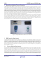
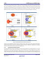
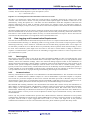
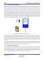
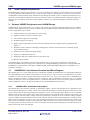
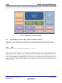
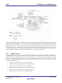
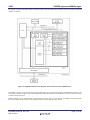
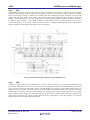
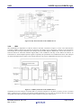
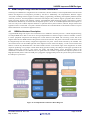
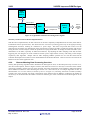
APPLICATION NOTE
V850
Renesas V850 MCU Improves BGM design
R01AN0213EU0100
Rev.1.00
May 13, 2011
Introduction
A Blood Glucose Meter (BGM) is a portable electronic device that automatically measures the level of blood glucose to
simplify the treatment of Type 1 diabetes (the type controlled via insulin) and to provide Type 2 diabetes patients with
information to help control their diet (the main form of treatment for Type 2). The device is appropriate for use in the
home and thus reduces the need for routine medical visits related to glucose monitoring. Additionally, advanced units
can provide measurement data to medical services automatically, via a wireless link, so that a complete history of
measurement data is available when medical visits do occur. This detailed and precise history can be invaluable in
diagnosing illness, identifying preventative treatment options and in tracking the progression of long-term illness.
The design of an effective BGM device must incorporate a wide range of functions: sensing of the blood sample,
computation to determine the glucose level in the blood, categorization of the measured result, logging of the stored
data, communication of the stored data to a medical service for follow-up consultation and a simple user interface to
display instructions, results and control BGM operation. Some designs might include an audio function to provide
prompts (either simple ‘beeps’ or via speech generated audio for visually impaired patients) that simplify device
operation. Because the BGM is to be used in the home, during travel or at the workplace it is important that it be small,
and use as little power as possible. Minimizing recharge and other ‘out of operation’ times is critical to providing
regular and easily accessed use, which is necessary for successful treatment.
BGM devices can also be extended to measure other blood components like ketones which are produced during
hyperglycemia. Measurements of other blood components can simply require a different test strip, with a different
active chemical. The BGM, which is now a more generic blood element meter, can be used to measure the amount of
the component using the same electronics.
This application note will cover the key features and functions required by a BGM device and will explore the
capabilities of the Renesas V850ES MCU that address these application requirements. The overall architecture of an
example BGM implementation will be developed and some of the key supporting functions- both in hardware and
software- will be described in detail. Key performance and power measurements will be included to help give the reader
a good understanding of the ability of the Renesas V850ES MCU to hit the power efficient processing requirements of
the application.
Target Device
V850ES/JG3-L
Table of Contents
1.
Blood Glucose Monitor Theory of Operation..................................................................................... 2
2.
BGM Operation Requirements.......................................................................................................... 2
3.
Renesas V850ES Peripherals used in BGM Design ........................................................................ 7
4.
BGM Example Design with the Renesas V850ES MCU................................................................. 14
5.
Conclusion....................................................................................................................................... 19
6.
References ...................................................................................................................................... 19
R01AN0213EU0100 Rev.1.00
May 13, 2011
Page 1 of 20
V850
1.
V850ES Improves BGM Designs
Blood Glucose Monitor Theory of Operation
A Blood Glucose Meter (BGM) is a medical device for measuring the concentration of glucose in the blood. It is one of
the key elements in the home blood glucose monitoring regime used by people with diabetes mellitus or hypoglycemia.
A small drop of blood, usually obtained by piercing the skin with a special sampling needle (a lancet), is placed on a
single-use test strip that the meter uses to determine the samples blood glucose level. After just a few seconds, the meter
displays the level in mg/dl or mmol/l to assist the user in determining the correct action to keep their glucose level
within the desired range. The metering process is typically done several times a day so that the target blood glucose
level stays within the desired range all day long in order to more effectively manage type 1 diabetes and type 2 diabetes
mellitus. This can reduce the occurrence rate and severity of both the long-term complications from hyperglycemia and
the short-term, potentially life-threatening complications of hypoglycemia.
Figure 1 shows four different generations of BGMs, and illustrates the improvements in size reduction and simplified
ease of use. Modern BGMs require much smaller blood samples, include lancets with adjustable depth to minimize
discomfort during sample collection, improved accuracy and speed of results, and include comprehensive data logging
and averaging functions to help track long term trends. Some systems can upload a history to a medical service to
advise the patient’s doctor of changes in glucose levels which might identify complications.
Figure 1: Example Blood Glucose Meters- Four Generations
2.
BGM Operation Requirements
A modern BGM must support several key features to be competitive in the marketplace. Perhaps the most critical
requirements are in these three key areas: the monitoring and computation used to determine the patient’s blood glucose
level and to recommend the right treatment; the logging and communication of measurement data to create a history of
results for use in long term preventative care; the user interface needed to simplify device operation and display of
results; and the device needs to operate in a variety of low power modes to extend battery life as much as possible.
These key requirements will be expanded on in the following sections so we can better identify the key components and
features needed in our design.
2.1
Glucose Metering Requirements
In order to better understand the requirements of blood glucose metering a quick review of the technique used to detect
blood glucose is useful. This technique can also be extended and used in a variety of other meters. Blood alcohol, gasses,
in-organic compounds and even radiation are just a few examples. Figure 2 shows a diagram of a typical four step
process used to measure the blood glucose level. In the first step a small sample of blood, containing Glucose (G) is
deposited on the test strip. The blood is routed to the electrodes via capillary action. Step 2 shows the circuitry attached
to the electrodes and the presence of the Mediator (M) enzyme on the test strip prior to the blood reaching the electrodes.
As illustrated in Step 3, the enzyme will react with the blood glucose (once the blood has moved down the test strip to
R01AN0213EU0100 Rev.1.00
May 13, 2011
Page 2 of 20
V850
V850ES Improves BGM Designs
the location with the enzyme near the electrodes) to create free electrons (e). The free electrons can be moved thru a
circuit (in this example when the switch is closed) when a voltage is applied between the two electrodes. The current
flow can be measured by a meter (A) in the circuit. The amount of charge that moves thru the circuit will be
representative of the blood glucose level in the sample. By integrating the current flow the total charge can be measured
and the blood glucose level calculated. The metering process typically only requires a few seconds- most modern
BGMs report results in less than 5 seconds- since the processing power required by the BGM is not extensive.
Figure 2: Example Blood Glucose Measurement Process
There are several refinements possible to the basic example given here. Once we get into the example implementation
section of this document some of these refinements will be described and implemented. Typically they only require
additional analog sensing channels, so the basic description given here is sufficient to understand the following
description of the analog sensing requirements of the BGM device.
2.1.1
Analog Sensing Requirements
In a typical BGM device there are a small number of electrodes used to measure the current generated by the test system
described above. These electrodes can be sensed by a variety of methods, but an Analog to Digital converter is usually
employed to convert the analog measurement to a digital value so it can be used in a numeric algorithm to determine the
amount of blood glucose present. The amount of current generated is typically around 10uA at the maximum point and
a simple conversion circuit is used to translate the electrode current into a voltage that can be easily measured by the
R01AN0213EU0100 Rev.1.00
May 13, 2011
Page 3 of 20
V850
V850ES Improves BGM Designs
AtoD converter. Because of the chemical reaction time, the current measurement takes a few second to complete.
Given that, a modern MCU with ADC with conversion times ranging from 5μS to 25μS is more than sufficient.
In addition to the current measurements described above, some additional sensor requirements can be added to the
design. For example, it is convenient to measure the presence of the test strip to make sure it has been inserted
completely. Since the measurement location of the blood sample is inside the meter, it is usually difficult to visually
determine if the strip is inserted completely. Some strips have registration markings to help improve strip placement,
but these are usually too small for the visually impaired. A simple sensor can be added to detect the presence of the strip
using an additional AtoD channel, so many designs include this feature. Alternately, many strip designs use a shorting
connector and GPIO to detect strip insertion.
Since each test strip has its own calibration code (due to the variations within processing batches) to improve
measurement accuracy it can be a requirement that the user input the test strip calibration code. Many test strip
containers include a small coding key that can be inserted into the BGM. These keys can use different resistance levels
on each of the key ‘fingers’ to make it easy to read the value with a few extra AtoD converters or with a small amount
of additional external circuitry to ‘multiplex’ these values to a single AtoD sense input.
Some advanced meters also include temperature monitoring since the method used to determine blood glucose levels
can vary based on the temperature. A simple thermistor (a temperature sensitive resistor) and an AtoD channel can be
used to measure the temperature near the electrodes within the BGM device.
2.1.2
Computation Requirements
Modern BGM devices require some basic computation functions in order to determine the results of a blood glucose
measurement. Many BGM companies have more sophisticated techniques which are proprietary and are part of the
Intellectual Property (IP) embodied in their design.
The typical response current from the example BGM sensor circuit shown in Figure 2 above is given in Figure 3 below.
The various phases of the response are:
1) Test Strip in inserted and a DC voltage is applied between the electrodes.
2) The blood sample is placed on the test strip and the blood begins to react with the enzyme to generate a current.
3) After the reaction ends the current begins to drop off. During this phase the current is diffusion controlled.
4) After 5 seconds has elapsed sensing is complete and results can be computed.
Figure 3: Typical BGM Response Current Profile
During the diffusion controlled step (3) the waveform shows a predictable downward decay that is defined by the
Cottrell Equation. This equation related the change in current over time, I(t), as a function of the number of electrons,
Faradays constant, the area of the electrode, the initial concentration of the substance under measurement and its
R01AN0213EU0100 Rev.1.00
May 13, 2011
Page 4 of 20
V850
V850ES Improves BGM Designs
diffusion coefficient. (The diffusion coefficient varies with temperature, but with a know temperature can be treated as a
constant). The full Cottrell Equation is given in Equation 1, below:
I(t) = -nFACo*Do1/2(πt)-1/2
Equation 1: Cottrell Equation for Determination of Current Over Time
The MCU can compute the current during the Cottrell period by periodically measuring the voltage on the AtoD
converter. Once the current is known over the period the Cottrell equation applies the number of electrons can be
determined by solving the equation for n. The MCU will have bandwidth to make this computation within the time
required. Adjustments can be made to eliminate various biases (for example if there are temperature changes or
impurities in the sample) to improve accuracy, but the use of the Cottrell equation is the baseline for most measurement
algorithms.
The timing of data collection can be critical in creating an accurate picture of the current changes over time. If hardware
timers are available that can be used to accurately capture AtoD conversion data periodically, without the need for CPU
intervention or time variable interrupt routines, accuracy in current measurement will improve. Precise time intervals
will insure that the time element is not a significant source of measurement errors.
2.2
Data Logging and Communication Requirements
Once the current measurement has been made and reported to the user it is important that the data not be lost. Logging
the measurement data and using it to identifying trends over long periods can be critical to improving home care and
minimizing unnecessary visits to the doctor. Trend data can also be useful during a periodic doctor visit or might even
be collected by a medical service so that the doctor can periodically check on patients results without needing a visit to
the clinic. More advanced systems might even issue alerts to the clinic if results indicate a change in treatment is
required. A communications system that allows the off-loading of logged data would be a critical component of this
type of advanced care system.
2.2.1
Data Logging
Data storage is important in order to store all the key data acquired during BGM use. This can include the basic result
(value and time of test) as well as more detailed metrics on the shape of the response curve, test strip production batch
numbers, self test and calibration readings. These more advanced readings might be useful for the manufacturer in
refining measurement algorithms, making updates to calibration routines and in determining the results of aging on the
elements of the system. Compression techniques could be used to store more data in a smaller memory. Data is
typically stored in non-volatile memory in FIFO fashion and can’t be accidentally erased or modified by the operator. It
is made available for to be downloaded to archival storage or displayed on the user interface in the form of averages
over specified time intervals or as graphs showing trends and long term changes in measurements.
2.2.2
Communications
Some key communications requirements can be identified for a full featured BGM device. The stored data can be made
available via a standard interface (USB for example) so it can be downloaded to a personnel computer or cell phone.
Once stored on a personnel computer the data can be archived and further processed to determine long term trends
(longer than the typical 500 or so measurements stored on the BGM). Trend data can be sent to a medical service or
clinic to monitor patient performance and alert the patient of any recommended changes in the treatment.
More detailed data including calibration, bias measurements and self-test data could be used by the manufacturer to
make changes in calibration routines and adjustment coefficients used by the blood glucose measurement algorithms.
These changes can be uploaded to the BGM to cancel aging and other effects that would create errors in future
measurements. Additionally, the BGM can be tailored more specifically to the patient and biases due to differences in
diet, the environment or activity levels can all be adjusted to further improve measurement accuracy and treatment
recommendations.
USB is only one possible communications protocol that a BGM could use. Infrared or Bluetooth are also possible
communications methods that could be used by advanced BGM devices. When a personnel computer is not available a
cell phone could be used to capture logged data and to send it to a clinic. This might even be the preferred
communication method for some users and could reduce the time a patient needed to spend on their daily routine.
R01AN0213EU0100 Rev.1.00
May 13, 2011
Page 5 of 20
V850
2.3
V850ES Improves BGM Designs
User Interface Requirements
Besides the main function of glucose measurement the BGM should also make it easy for the user to make
measurements, check on the time for the next measurement, view measurement history, determine the results of
measurements, and maximize battery life, all with a small and convenient design. A simple user interface with a clear
display is an important factor in improving device usability and must be a key element integrated into the overall design.
In order to produce more accurate results, devices can also include self-test functions, calibration functions using
samples with known blood glucose levels and can include measurements of environmental factors such as temperature
to adjust the metering algorithms and adjust for component aging effects. Typically each batch of test strips has
different characteristics and the BGM must be correctly calibrated for each batch. The batch number can either be
entered into the BGM manually or can be read off a special key included with each vial of strips. The key is inserted
into the BGM and the calibration code is displayed prior to each test so the operator can compare the calibration value
to the one listed on the vial. An example of a key-based coding system is diagrammed in below Figure 4 . This example
uses the small key (with the code 237 printed on it, shown in the upper left of Figure 4 ), that is included in the vial of
test strips (shown in the bottom left of Figure 4 ). The user inserts the key and then before each test compares the key
value (shown on the BGM display in Figure 4 ) to the value printed on the container.
Figure 4: Example Key-based Coding System
In some devices it can be useful to have an audio alarm or alert function. This can indicate the time to take a
measurement or the result of a measurement outside of the normal range. Specialized units could even provide the result
via speech synthesis for the visually impaired. Many modern units also keep the history of the last measurements,
usually a few hundred, and can show graphs or averages over several useful time intervals. These reports can help
identify long term trends and identify possible changes in health that could be difficult to catch when results are only
viewed over the short term. The user interface should make it easy to view these reports with a minimum of operator
intervention.
It is useful for the BGM to also include a time of day function to make it convenient for the user to know when to take a
measurement and so the BGM can include a time of day function also supports time-stamping data for data logging,
ensuring proper clinical analysis of the measurement. A hardware-based Real Time Clock (RTC) makes the
implementation of a clock function easy and reduces the CPU processing burden.
2.4
Low Power Requirements
When the BGM is not in use, it only needs to keep track of a real time. In this operating mode, it is desired to have the
entire system turned off, except the Real Time Clock which tracks the real time. Even in RUN mode, there are times
for high processing and low processing. A flexible clock with easy transition between different operation frequency
can tailor to power consumption. For example, running USB would put MCU at max frequency, while actual
processing may run at 8Mhz. During the design implementation we will explore the ways we can use low power modes
to reduce power consumption and will provide some measurements for an example design.
R01AN0213EU0100 Rev.1.00
May 13, 2011
Page 6 of 20
V850
2.5
V850ES Improves BGM Designs
Small Footprint Requirement
The BGM should be able to be carried easily in a pocket or small purse. Targeting a system with the size of a cell phone
is a key requirement. If the BGM is not easy to carry around it will not be used as much as it needs to be. Thus the size
of the BGM is important and the design should focus on reducing the number of device components and use devices in
small sizes (such as FBGA), resulting in a small circuit board, to achieve a portable form factor. NOTE the display size
must take into consideration use by the visually impaired, and may even include small speaker to announce Glucose
readings.
3.
Renesas V850ES Peripherals used in BGM Design
The Renesas processor product line is very extensive with a wide range of features and target applications. For a BGM
design it will be important for the processor to address the key requirements described in the previous section. A list of
the key requirements is given below:
1) Analog to Digital conversion support for sensor inputs
2) Digital to Analog conversion for audio output
3) User interface support for LCD display
4) Peripheral support for USB 2.0
5) DMA support to off load the processor from the mundane work of moving data between peripherals and
memory
6) Hardware counters and times (including watchdog timer, real time clock and timers for controlling analog
capture and generation)
7) Small device size- FBGA package preferably
8) Support for computation functions
9) High quality and secure Flash with Error Correction Code
10) Robust software support
The V850ES/Jx3-L with USB line of devices that provide the low-power operation, peripheral set, small device
footprint (8x8 FBGA) and processing power required for our example BGM design. The amount of on-chip RAM and
Flash Memory required will be in the range of 256KB-512KB of Flash and 40KB of RAM so the V850ES/JG3-L is a
good fit for our design.
3.1
V850ES/JG3-L Architecture Overview and Block Diagram
The V850ES/JG3-L is a 32-bit single-chip microcontroller that includes the V850ES CPU core and peripheral functions
such as ROM/RAM, timer/counters, serial interfaces, an A/D converter, a D/A converter, and USB function controller.
In addition to high real-time response characteristics and the basic one clock cycle instructions, the V850ES/JG3-L
features multiply instructions, saturated operation instructions, and bit manipulation instructions. It is an optimal
solution for real-time control, PC peripheral devices, or industrial instruments. Let’s look at the key hardware elements
of the V850ES/JG3-L prior to diving into the description of the BGM high-level architecture.
3.1.1
V850ES/JG3-L Architecture Description
The V850ES/JG3-L key hardware elements are illustrated in Figure 5, below. The peripheral set is comprehensive and
includes System Management, Analog, Timers and Communications hardware. System Management functions include
a Bus Control Function that manages the general purpose I/O ports, a four-channel Direct Memory Access Controller
(DMAC) that supports both internal and external transfer requests and a Standby mode controller that manages the
seven low power operation modes. Analog functions include twelve channels of 10-bit resolution Analog to Digital
Converter (ADC) with 5uS minimum conversion time, and two channels of 8-bit resolution Digital to Analog Converter
(DAC) with 3us minimum conversion time. Timer functions include three 16-bit General Purpose timer/counters (GP
Timers) each with multiple channels, a Watchdog Timer (WD Timer) that issues a system reset or interrupt on overflow,
a clock generator (Clock) that creates the various clock signals used by the CPU and peripherals, and a Real Time Clock
(RTC) to keep track of the time and date.
R01AN0213EU0100 Rev.1.00
May 13, 2011
Page 7 of 20
V850
V850ES Improves BGM Designs
Communications functions include a Universal Serial Bus (USB) function controller, seven channels of Asynchronous
Serial Interface (UART), and three channels of Inter IC (IIC) communications bus.
Figure 5: V850ES/JG3-L Key Hardware Blocks
3.2
Detailed Description of Key Common Hardware Blocks
In order to better understand our BGM implementation it is necessary to describe the operation of several of the key
hardware blocks of the V850ES/JG3-L. These blocks will be used to implement the required features of the BGM
device.
3.2.1
ADC
A block diagram of the key elements of the V850ES/JG3-L is shown in
Figure 6. It has 12 analog inputs, 12 storage registers (ADA0CR[0:11] for the converted data, an analog selector,
sample and hold circuit, comparator, and a 10-bit D-to-A converter used by the successive approximation register to
determine the value on the selected analog input. Additional circuitry supports power fail detection functions. The
Power Fail Threshold Registers (ADA0PFT/M) are used by the power fail controller to determine when the power level
has crossed the fail threshold and issues an interrupt. Conversion time is largely based on the ADC clock selected. In
addition, ADC has a high-speed mode, and the reader is directed to the Users manual for additional detail (see
references section).
R01AN0213EU0100 Rev.1.00
May 13, 2011
Page 8 of 20
V850
V850ES Improves BGM Designs
Figure 6: ADC Block Diagram Renesas V850ES/JG3-L
The ADC Start Trigger signal (ADTRG) can be sourced from a Timer so that conversions can be done at regular
intervals without the use of processor bandwidth. The ADC can also issue an interrupt signal (ADI) that the Direct
Memory Access Controller (DMAC) can use to initiate a transfer. This will also reduce processor load. The complete
data capture chain, including the ADC, Timer, DMAC and power failure detection is explained in detail in the
implementation section of this application note.
3.2.2
General Purpose Timers
The General Purpose Timers can be used to implement a very wide set of functions. The V850ES/JG3-L has three main
timers, each with slightly different characteristics.
16-bit Timer/Event Counter P (TMP): TMP has 6 timer/event channels with two compare registers per channel. Each
channel has the following functions: Interval timer, external event counter, external trigger pulse output, one-shot pulse
output, PMW output, free running timer and pulse width measurement.
16-bit Timer/Event Counter Q (TMQ): TMQ is a single channel with four compare registers (twice the number as TMP)
with, otherwise, the same functions as TMP.
16-bit Interval Timer M (TMM): TMM is a dedicated interval timer that generates interrupt requests at a specified
interval selected from one of eight clock sources: the main clock (fxx), a divided main clock (fxx/2, fxx/4, fxx/64,
fxx/512), the watch timer interrupt signal (INTWT), the internal 200kHzclock (fR/8), and the subclock (fXT = 32kHz,
typically used for tracking real time).
Each timer channel has a variety of holding registers, control resources and several shared clocking signals used to drive
the counting/timing functions. Timer outputs can be used to generate interrupts, start ADC converters, or to drive output
pins directly. A typical timer channel for the V850ES/JG3-L is shown in Figure 7 below (TMP is used as the example).
The channel input/output pins can be used to drive the timer counter hardware to start a timer or increment a count.
Each channel has a 16-bit counter used to count internal clocks and external events, a read buffer register (TPnCNT)
capture/compare registers (TPnCCR0/1), CCR buffer registers, control registers (TPnCTL0/1, not shown in the
diagram), and an edge detector to identify edge events used to trigger the timer/counter.
R01AN0213EU0100 Rev.1.00
May 13, 2011
Page 9 of 20
V850
V850ES Improves BGM Designs
Figure 7: Typical Timer Counter Channel Block Diagram
In a typical BGM design, ADC must sample at a precise interval to track the settling current measurement as the blood
glucose reacts with the chemistry. The accuracy of the interval has direct impact to the computation algorithm, where
measured current data is fitted to a curve. Any errors in timing could generate false results and trigger an incorrect
treatment for the patient. The ability of the timer to directly trigger an interrupt to start the ADC creates a true periodic
representation of the current measurement. This provides a deterministic behavior that is not possible in the case where
the CPU has to process the timer interrupt and start the ADC. The complete data capture chain, including the ADC,
Timer and DMAC is explained in detail in the implementation section of this application note.
3.2.3
DMA Controller
The V850ES/JG3-L has a feature-rich four channel Direct Memory Access Controllers (DMACs) to simplify data
transfer between functional units. The DMAC controls data transfer between memory and I/Os, between memories, or
between I/Os based on DMA requests issued by on-chip peripheral I/O (serial interfaces, timer/counters, and A/D
converter), interrupts from external input pins, or software triggers (memory refers to internal RAM or external
memory). A simplified block diagram of the key DMAC elements used in our design is shown in Figure 8 below. The
key registers in the DMAC are:
•
DMA source address registers 0 to 3 (DSA0 to DSA3)
•
DMA destination address registers 0 to 3 (DDA0 to DDA3)
•
DMA transfer count register 0 to 3 (DBC0 to DBC3)
•
DMA addressing control registers 0 to 3 (DADC0 to DADC3)
•
DMA channel control registers 0 to 3 (DCHC0 to DCHC3)
•
DMA trigger factor registers 0 to 3 (DTFR0 to DTFR3)
R01AN0213EU0100 Rev.1.00
May 13, 2011
Page 10 of 20
V850
V850ES Improves BGM Designs
The DMAC operates with either single or double transfers and with fixed priority (DMA channel 0 is highest and DMA
channel 3 is lowest).
Figure 8: Simplified DMAC Block Diagram of Key Elements of the V850ES/JG3-L
The DMAC connects to the On-chip Peripheral and Internal bus so that transfers between peripherals and memory can
be supported without using the CPU. The management of individual transfers is handled by the control blocks- Channel
Control and Count Control.
DMAC transfers can be initiated from a peripheral unit, like the ADC, via an interrupt. The DMAC will then transfer
the converted data to the location of the memory buffer associated with the input stream.
R01AN0213EU0100 Rev.1.00
May 13, 2011
Page 11 of 20
V850
3.2.4
V850ES Improves BGM Designs
RTC
The V850ES/JG3-L RTC, shown in Figure 9 has a wealth of counters, alarm and control registers that can be used to
display the time and date as well as time stamp data logging operations by the BGM. A separate sub-clock oscillator
and pre-scaled clock, running at 32KHz, are included in the RTC minimizing external component count. Second,
minute, hour and date counters can be used as the time/date display and logging time stamp. Without a Real Time
Counter, a MCU would have to use a timer that triggers a ½ second interrupt. When interrupted, the MCU would have
to update the time in memory. For a BGM, of which is used to measure every 4-5 hours (pls check to see if this is
correct), waking up every ½ second consumes unnecessary power. Having a dedicated Real Time Clock hardware
function simplifies software design with reduce power consumption.
Figure 9: Real Time Clock Key Elements in the V850ES/JG3-L
3.2.5
DAC
The DtoA Converter (DAC) in the V850ES/JG3-L is shown in Figure 10. There are two 8-bit output channels on the
DAC and the maximum conversion time is 3uS. The DAC Data Registers (DA0CS1 and DA0CS0) hold the data value
to be converted on the associated output channel. The Data Registers are accessed via the Internal bus and they are
readable as well as writable. The DAC Conversion Mode Registers (DA0MD1/0, DA0CE1/0) specifies the Enable
condition for each channel and for the DAC module. (The analog output voltage is referenced to the AVref supply
which defines the high voltage limit of the DAC outputs). The DAC uses a resistor ladder architecture to generate the
analog outputs. The DAC can operate in either normal mode (by writing directly to the data register) or in real-time
mode using an interrupt request signal as the trigger.
R01AN0213EU0100 Rev.1.00
May 13, 2011
Page 12 of 20
V850
V850ES Improves BGM Designs
Figure 10: Key DAC Functions in the V850ES/JG3-L
3.2.6
USB
The V850ES/JG3-L implements a USB 2.0 function controller, illustrated in Figure 11 below. The USB Function
Controller (USBFC) manages the operation of the block. The bridge circuit connects the controller to the internal bus
and manages the interrupts (identified by the Bridge Interrupt Enable Register (BRGINTE) used for data transfers. A
USB 2.0 transceiver and Serial Interface Engine (SIE) is also included on the chip so this reduces the need for an
external device. All the endpoint specific registers required by the specification are included in the block. The USB port
can utilize the DMA transfer engine so that transfer functions can progress independent from processor intervention.
Figure 11: USB Key Functions in the V850ES/JG3-L
The BGM can use the USB port to transfer data to a personnel computer or cell phone to archive, process or transmit
data to a medical service company. The amount of data transferred is not very large so connection times are small when
using USB. This reduces the time the patient needs to dedicate to this part of the process.
R01AN0213EU0100 Rev.1.00
May 13, 2011
Page 13 of 20
V850
4.
V850ES Improves BGM Designs
BGM Example Design with the Renesas V850ES MCU
The design of a BGM device using Renesas microcontrollers, like the V850ES, is much simplified due to the advanced
features and high level of integration provided by the device. Additionally, the comprehensive Renesas support
‘ecosystem’ including software support tool chain (design, programming, and debug), development platforms (boards
with host processors, external peripheral connections and example code), software support (peripheral driver libraries,
signal processing libraries and operating systems), knowledgeable field engineering support and extensive product
documentation dramatically accelerates the development process. (Note: in our BGM implementation description we
will cover only a few of these important elements- in particular the key device features, libraries, design software and
application notes- but the other ‘ecosystem’ elements should not be overlooked. Refer to the Renesas website to explore
all the elements not covered in this application note).
4.1
BGM Architecture Description
A typical BGM design will require some external devices in addition to the main processor. A block diagram showing
an example BGM device that we will use as our target implementation is shown in Figure 12 below. The MCU connects
to all the peripheral components and manages the overall function of the BGM. The Test Strip, on the left of the
diagram slides into the BGM and the Analog Sensors measure the reaction. The power control block in the lower left of
the diagram keeps the units battery charged and supports the low power control modes selected by the V850ES. The
user interface shown on the middle right side of the diagram consists of the LCD display, a touch screen interface and
buttons to initiate key BGM functions. The audio interface shown on the bottom right of the diagram has an audio
output for producing voice prompts or audio alerts during operation. Finally, the USB port in the upper right side of the
diagram connects the system to a PC archive test results. The USB interface circuit, described in detail in the
V850ES/JG3-L Hardware Users Manual, uses two gates and a few resistors to signal that the endpoint operates in the
High-Speed mode, detects when the USB port is plugged or unplugged and protects the system when powered off and
the USB port is powered on.
Figure 12: Example BGM Architecture Block Diagram
R01AN0213EU0100 Rev.1.00
May 13, 2011
Page 14 of 20
V850
V850ES Improves BGM Designs
The MCU will implement the signal processing algorithms used to determine the result of the blood glucose
measurement. The user interface and overall operational flow is also controlled by the MCU and uses a variety of
internal peripherals like the previously described DMAC, DAC, ADC, RTC, and MTU.
4.2
Key Features for the Example BGM
The two most important features of the Blood Glucose Meter are the ability to do quick and precise self tests or
calibrations and the actual measurement of the Blood Glucose Level. The self-test feature should be able to run without
a calibration
4.2.1
Self-Test
The self-test function measures the performance of the hardware elements of the BGM to insure that measurements
made on the device are as accurate as possible. The normal hardware self-tests should be implemented to check for PCB
connections and key device functions like timing, power down modes, voltage references, memory reliability and other
important hardware operations. Self-test for the sensor should include verification that PCB traces are solid, but should
also check for noise or other less obvious effects that could result in inaccurate measurements.
In addition to self-tests, device features, like watch dog timers, should be used to improve software robustness and
system reliability. Finally the device should include an LCD test which turns on all the segments to avoid reading
errors such as a 7 with missing segment begin read as a 1. It is important to catch any system issues prior to making a
measurement which could result in an incorrect treatment or unnecessary service call or doctor visit.
4.2.2
Calibration
The calibration feature is actually very similar to the actual measurement, but it uses a known amount of reactant that
can be used to calibrate the sensors and the measurement algorithm. This is important to do periodically so that further
measurements are as fast and accurate as possible. Calibration will measure a known sample and then update, if
necessary, the constants used to adjust for aging of the sensors. These constants can be tracked over time, in a similar
way to the actual measurements, to provide device aging information to the manufacturer. The analysis of the trends in
calibration results will be useful in making changes to the next design that can help improve sensor accuracy.
There is no functional difference, as far as our design is concerned, between calibration and measurement, so the
functional details will be covered in the Measurement section below.
4.2.3
Blood Glucose Measurement
The blood glucose measurement function can be broken into two major function- data collection and data processing.
These functions will be described, along with their implementation in our example design, in the following sections.
4.2.4
Data Collection Function Overview
One of the key signal processing paths is from the external sensors to the input to the algorithm that calculates the
patient’s glucose level. Typically the captured data will be deposited in a buffer memory that can be accessed by the
signal processing algorithm, that is somewhat independent of the data collection process. This will allow for a modular
implementation where one function can focus on acquiring the data and another function can focus on the data
processing. In the next section of the application note we will look into the implementation details of the data sensing,
collecting and storing of the acquired data. Once this portion of the algorithm is better understood we will look at the
signal processing part of the algorithm data is actually analyzed.
4.2.5
Data Collection Implementation
Data can be collected from the ADC into a buffer autonomous from the CPU. This is done by “ticking” the ADC with a
timer set up to activate the ADC at prescribed intervals. The ADC completion will then be used to activate the DMA
and move the data into the prescribed buffer. DMA completion interrupt may be set in such a manner that the software
is notified whenever 3-4 samples are collected so the analysis task can do peak and slope detection, or it can collect all
the data for the prescribed time and then “Wake up” the Analysis task. This is shown in diagrammatically in Figure 13.
R01AN0213EU0100 Rev.1.00
May 13, 2011
Page 15 of 20
V850
V850ES Improves BGM Designs
TMP2
Compare
Match 0
AD Trigger
AD Complete
AN0
ADC
Memory
Buffer
DMAC
Complete Intr
Data to
Current
Detection
Task
Figure 13: Typical Data Collection for Analog Sensor Signals
Summary of Sensor Data Collection Implementation
With the above implementation, the data collection can be done completely independent from the CPU (other than for
initialization and set-up instructions). This allows the CPU to focus its processing power only on the signal processing
and diagnostic functions, resulting in a reduction in power usage. The timer can provide finer control over the
sampling interval and also, the determinism of the timer directly triggering the ADC provides the samples with precise
timing for more accurate analysis without the problems of relying on the MCU to manage the timers and ADC. (nondeterministic in the MCU, especially in RTOS environments). By adjusting the ADC sampling clock and, the timer
triggering rate, the designer can strike a balance between power usage and the accuracy and timing of the samples
required by their algorithm. Sample code for ADC sampling, DMAC operation for use with the V850 and the
Cubesuite development environment can be downloaded from the Renesas Website. All these resources are listed in the
Reference section of this application note.
4.2.6
Glucose Metering Data Processing Overview
The key data processing algorithm used to determine the blood glucose level, as described previously in section 2.1.2,
uses the Cottrell equation, shown in Figure 14 below, that relates the current over time I(t) as a function of the number
of electrons, Faradays constant, the area of the electrode, the initial concentration of the substance under measurement
and its diffusion coefficient. After measuring the current over a time interval (in our example algorithm we take 10
measurements over a 3.2sec interval, as shown by the x’s in Figure 14 ) and using the known constants (Faradays
constant, area of the electrode, the initial concentration of the substance and its diffusion coefficient) the number of
electrons (n) can be determined. The number of electrons will then give us the concentration of the blood glucose in the
sample.
R01AN0213EU0100 Rev.1.00
May 13, 2011
Page 16 of 20
V850
V850ES Improves BGM Designs
Figure 14: Cottrell’s Equation and BGM Measurements to Determine Glucose Levels
4.2.7
Data Processing Implementation
The main data processing algorithm needed to determine the number of electrons uses a curve fitting procedure to map
the 10 measurements to the Cottrell equation. A mapping like that shown in Figure 15 can be accomplished using a trial
and error approach with values for the number of electrons (n) being tried and adjusted until the error measurement
(distance of the actual measurements from the predicted value) is a minimum. Usually the initial value can be guessed
based on previous readings and then quickly adjusted to zero-in on the actual measurement. In the case of an initial
reading, a typical value can be used to start the process.
The computations required by the algorithm are fairly simple (multiply, divide and square root) and can be further
simplified by using look-up tables for key values like (πt)-1/2and adjustments to constants due to calibration, temperature
and batch processing differences. With 10 data points to fit, and a fitting algorithm that closes the error by 50% on each
iteration, it should take less than 10 passes to get to an optimal value for the measurement. This should not require more
than a fraction of the V850ES processor bandwidth. Notice that curve fitting can begin even before all the
measurements are taken if measurement time is important to minimize. After four or five measurements curve fitting
can begin, with additional measurements added to the data set as they come in.
4.2.8
Power Management Overview
Controlling the power used by the BGM will be critical to extend battery life and ensure accuracy of measurement. . If
battery life is too short, the user will miss a scheduled measurements because he has to recharge the battery. Power
management can easily be performed using simple state machines in software. The application knows the power level
and performance level it must be at to properly execute the current active tasks. Ideally power saving would be done
simply and easily and in such a way that key functions would not be impacted.
NOTE: Most BGMs will have battery indicator to notify user that battery must be recharged. In most cases, the meter
will not allow or perform measurements in this state due to possible errors.
4.2.9
Power Management Implementation
The V850ES/JG3-L has several low power operation modes that can help reduce power consumption and extend battery
life. These modes are:
HALT: Only the operating clock of the CPU is stopped, the peripherals are still on. The total current consumption
of the system can be reduced by using this mode in combination with the normal operation mode for intermittent
operation.
R01AN0213EU0100 Rev.1.00
May 13, 2011
Page 17 of 20
V850
V850ES Improves BGM Designs
IDLE1: All the operations of the internal circuits except the oscillator, PLL and flash memory are stopped. This
mode can reduce the power consumption to a level lower than the HALT mode because it stops the operation of
most of the on-chip peripheral functions. Some peripherals can be left operational.
IDLE2: All the operations of the internal circuits except the oscillator are stopped. This mode can reduce the power
consumption to a level lower than the IDLE1 mode because, in additional to IDLE1, it powers off the Flash
memory.
STOP: All the operations of the internal circuits except the sub-clock oscillator (32kHz) are stopped. The subclock oscillator can be turned off is desired. This mode can reduce the power consumption to a level lower than the
IDLE2 mode. In the low-voltage STOP mode power consumption decreases further because the voltage of the
regulator is lowered. Note that the data of the internal RAM and the values of the CPU registers are being held in
STOP mode.
Sub-clock Operation: The sub-clock (32kHz) is used as the internal system clock. This mode can reduce the
power consumption to a level lower than the normal operation mode because of the lower operating frequency.
There is a low-voltage sub-clock operation mode in which power consumption decreases further because the
voltage of the regulator is lowered.
Sub-IDLE: All the operations of the internal circuits except the oscillator, PLL and flash memory are stopped, in
the sub-IDLE operation mode. The total current consumption of the system can be reduced by using this mode in
combination with the Sub-clock mode for intermittent operation.
Low Voltage Sub-IDLE: In low-voltage sub-IDLE mode power consumption decreases. The Main clock and PLL
are stopped. Additional functions are stopped (see hardware manual for details) and power is reduced further
because the voltage of the regulator is lowered.
RTC backup: The RTC continues counting on the 32kHz clock using the current supplied by the backup voltage
to the RVDD. The power consumption in this mode is even lower than in low-voltage STOP mode. Note that the
data of the internal RAM and the values of the CPU registers cannot be held in RTC backup mode.
Earlier we talked about using simple state machine to determine the power levels and performance required. It is a
good design practice to map a function and tasks to a specific power modes. For example, when USB is used to
communicate data, the MCU should operate in RUN mode as it is powered off the USB port and communications can
be performed quickly (not to mention the USB clocking requirements). After communicating, we can switch to back to
RTC mode to keep time and conserve battery power . The push of a button may “wake up” the device into one of the
low power modes to do switch / key scanning. Strip insertion and may put it in to a higher performance mode to do the
data collection and analysis, finally going into a mode that preserves the display until the stick is ejected and the device
can return to RTC mode.
In the Normal operation mode, HALT, which only stops the CPU, could be used to save power. For example, if the
peripheral is performing the data acquisition function, the processor can be halted. After the acquisition period is over,
the timer can trigger a interrupt to wake up the processor to read the data from the ADC converter. As another example, ,
if curve fitting is going on in parallel with data acquisition, the CPU can finish the data computation function before the
next data is available. At that time, the CPU can be halted until the next measurement is ready. Sub Clock Operation
or Low-Voltage Sub-Clock operation can be considered when the processing required does not need a faster clock cycle.
Lower power might be achieved by simply operating the MCU at a lower clock rate, say 3Mhz instead of the full
16MHz, during the entire function instead of the intermittent use of the Halt mode. Some amount of experimentation
can be used to determine the right mix based on a suite of typical use examples.
.
R01AN0213EU0100 Rev.1.00
May 13, 2011
Page 18 of 20
V850
4.2.10
V850ES Improves BGM Designs
Sample Power Measurements
Table 1 give some of the power numbers for the V850 referenced in this document for the in the various operational and
low power modes. Power measurements can be greatly affected by your board design, so you numbers may be different
and standard practices for low power design should be implemented.
Clock / Mode
Current (measured)
16MHz + USB
21.4mA
16MHz
15.6mA
6MHz
4.71mA
3Mhz
2.85mA
1.5MHz
1.93mA
32kHz CPU Operating
15uA
STOP
3.5uA
Comments
RTC Active
Table 1: Power Measurements
Note: The data in was empirically obtained using the V850 Low power demo boards and should not be used for
design reference. Refer to the device User’s Manual: Hardware for supply current (Idd) specifications in the
various modes of operation (see reference section).
5.
Conclusion
This application note has shown the Renesas V850ES MCU provides the power efficient implementation required for a
mid-range BGM design. Combining various clock speeds and standby modes, you can meet both your computational
horsepower and battery life requirements. With the extensive Renesas ‘ecosystem’ of software development tools,
signal processing libraries, drivers, operating system support, starter kits, example code and application notes the
designer can focus on the development of the metering algorithm and data logging functions required to differentiate a
BGM in the marketplace. The list of resources in the next section is just an example of the types of ‘ecosystem’
elements Renesas provides to accelerate a BGM design. Renesas also provides additional support for display solutions,
touch user interface, audio and connectivity solutions that can be key components of advanced BGM systems. For a
more complete list of applicable resources visit the Renesas Healthcare web page at the following url:
http://am.renesas.com/applications/medical/medical_category_landing.jsp
6.
References
Application Note, V850ES/JG2 #U18676EJ1V0AN00
Preliminary Datasheet, V850ES/JG3-L, # R01DS0030EJ0001
User’s Manual , V850ES/JG3-L, # U18953EJ5V0UD00
Useful Additional Reading:
http://america2.renesas.com/news/newsdetail.html?page=low_power_32-bit_v850_mcus_for_portable_devices
R01AN0213EU0100 Rev.1.00
May 13, 2011
Page 19 of 20
V850
V850ES Improves BGM Designs
Website and Support
Renesas Electronics Website
http://www.renesas.com/
Inquiries
http://www.renesas.com/inquiry
Revision Record
Rev.
1.00
Date
May.13.2011
Description
Page
Summary
—
First edition issued
All trademarks and registered trademarks are the property of their respective owners.
R01AN0213EU0100 Rev.1.00
May 13, 2011
Page 20 of 20
General Precautions in the Handling of MPU/MCU Products
The following usage notes are applicable to all MPU/MCU products from Renesas. For detailed usage notes on the
products covered by this manual, refer to the relevant sections of the manual. If the descriptions under General
Precautions in the Handling of MPU/MCU Products and in the body of the manual differ from each other, the
description in the body of the manual takes precedence.
1. Handling of Unused Pins
Handle unused pins in accord with the directions given under Handling of Unused Pins in the manual.
⎯ The input pins of CMOS products are generally in the high-impedance state. In operation with an
unused pin in the open-circuit state, extra electromagnetic noise is induced in the vicinity of LSI, an
associated shoot-through current flows internally, and malfunctions occur due to the false
recognition of the pin state as an input signal become possible. Unused pins should be handled as
described under Handling of Unused Pins in the manual.
2. Processing at Power-on
The state of the product is undefined at the moment when power is supplied.
⎯ The states of internal circuits in the LSI are indeterminate and the states of register settings and
pins are undefined at the moment when power is supplied.
In a finished product where the reset signal is applied to the external reset pin, the states of pins
are not guaranteed from the moment when power is supplied until the reset process is completed.
In a similar way, the states of pins in a product that is reset by an on-chip power-on reset function
are not guaranteed from the moment when power is supplied until the power reaches the level at
which resetting has been specified.
3. Prohibition of Access to Reserved Addresses
Access to reserved addresses is prohibited.
⎯ The reserved addresses are provided for the possible future expansion of functions. Do not access
these addresses; the correct operation of LSI is not guaranteed if they are accessed.
4. Clock Signals
After applying a reset, only release the reset line after the operating clock signal has become stable.
When switching the clock signal during program execution, wait until the target clock signal has
stabilized.
⎯ When the clock signal is generated with an external resonator (or from an external oscillator)
during a reset, ensure that the reset line is only released after full stabilization of the clock signal.
Moreover, when switching to a clock signal produced with an external resonator (or by an external
oscillator) while program execution is in progress, wait until the target clock signal is stable.
5. Differences between Products
Before changing from one product to another, i.e. to one with a different type number, confirm that the
change will not lead to problems.
⎯ The characteristics of MPU/MCU in the same group but having different type numbers may differ
because of the differences in internal memory capacity and layout pattern. When changing to
products of different type numbers, implement a system-evaluation test for each of the products.
Notice
1.
All information included in this document is current as of the date this document is issued. Such information, however, is subject to change without any prior notice. Before purchasing or using any Renesas
Electronics products listed herein, please confirm the latest product information with a Renesas Electronics sales office. Also, please pay regular and careful attention to additional and different information to
be disclosed by Renesas Electronics such as that disclosed through our website.
2.
Renesas Electronics does not assume any liability for infringement of patents, copyrights, or other intellectual property rights of third parties by or arising from the use of Renesas Electronics products or
technical information described in this document. No license, express, implied or otherwise, is granted hereby under any patents, copyrights or other intellectual property rights of Renesas Electronics or
others.
3.
You should not alter, modify, copy, or otherwise misappropriate any Renesas Electronics product, whether in whole or in part.
4.
Descriptions of circuits, software and other related information in this document are provided only to illustrate the operation of semiconductor products and application examples. You are fully responsible for
the incorporation of these circuits, software, and information in the design of your equipment. Renesas Electronics assumes no responsibility for any losses incurred by you or third parties arising from the
use of these circuits, software, or information.
5.
When exporting the products or technology described in this document, you should comply with the applicable export control laws and regulations and follow the procedures required by such laws and
regulations. You should not use Renesas Electronics products or the technology described in this document for any purpose relating to military applications or use by the military, including but not limited to
the development of weapons of mass destruction. Renesas Electronics products and technology may not be used for or incorporated into any products or systems whose manufacture, use, or sale is
prohibited under any applicable domestic or foreign laws or regulations.
6.
Renesas Electronics has used reasonable care in preparing the information included in this document, but Renesas Electronics does not warrant that such information is error free. Renesas Electronics
7.
Renesas Electronics products are classified according to the following three quality grades: "Standard", "High Quality", and "Specific". The recommended applications for each Renesas Electronics product
assumes no liability whatsoever for any damages incurred by you resulting from errors in or omissions from the information included herein.
depends on the product's quality grade, as indicated below. You must check the quality grade of each Renesas Electronics product before using it in a particular application. You may not use any Renesas
Electronics product for any application categorized as "Specific" without the prior written consent of Renesas Electronics. Further, you may not use any Renesas Electronics product for any application for
which it is not intended without the prior written consent of Renesas Electronics. Renesas Electronics shall not be in any way liable for any damages or losses incurred by you or third parties arising from the
use of any Renesas Electronics product for an application categorized as "Specific" or for which the product is not intended where you have failed to obtain the prior written consent of Renesas Electronics.
The quality grade of each Renesas Electronics product is "Standard" unless otherwise expressly specified in a Renesas Electronics data sheets or data books, etc.
"Standard":
Computers; office equipment; communications equipment; test and measurement equipment; audio and visual equipment; home electronic appliances; machine tools;
personal electronic equipment; and industrial robots.
"High Quality": Transportation equipment (automobiles, trains, ships, etc.); traffic control systems; anti-disaster systems; anti-crime systems; safety equipment; and medical equipment not specifically
designed for life support.
"Specific":
Aircraft; aerospace equipment; submersible repeaters; nuclear reactor control systems; medical equipment or systems for life support (e.g. artificial life support devices or systems), surgical
implantations, or healthcare intervention (e.g. excision, etc.), and any other applications or purposes that pose a direct threat to human life.
8.
You should use the Renesas Electronics products described in this document within the range specified by Renesas Electronics, especially with respect to the maximum rating, operating supply voltage
range, movement power voltage range, heat radiation characteristics, installation and other product characteristics. Renesas Electronics shall have no liability for malfunctions or damages arising out of the
use of Renesas Electronics products beyond such specified ranges.
9.
Although Renesas Electronics endeavors to improve the quality and reliability of its products, semiconductor products have specific characteristics such as the occurrence of failure at a certain rate and
malfunctions under certain use conditions. Further, Renesas Electronics products are not subject to radiation resistance design. Please be sure to implement safety measures to guard them against the
possibility of physical injury, and injury or damage caused by fire in the event of the failure of a Renesas Electronics product, such as safety design for hardware and software including but not limited to
redundancy, fire control and malfunction prevention, appropriate treatment for aging degradation or any other appropriate measures. Because the evaluation of microcomputer software alone is very difficult,
please evaluate the safety of the final products or system manufactured by you.
10. Please contact a Renesas Electronics sales office for details as to environmental matters such as the environmental compatibility of each Renesas Electronics product. Please use Renesas Electronics
products in compliance with all applicable laws and regulations that regulate the inclusion or use of controlled substances, including without limitation, the EU RoHS Directive. Renesas Electronics assumes
no liability for damages or losses occurring as a result of your noncompliance with applicable laws and regulations.
11. This document may not be reproduced or duplicated, in any form, in whole or in part, without prior written consent of Renesas Electronics.
12. Please contact a Renesas Electronics sales office if you have any questions regarding the information contained in this document or Renesas Electronics products, or if you have any other inquiries.
(Note 1)
"Renesas Electronics" as used in this document means Renesas Electronics Corporation and also includes its majority-owned subsidiaries.
(Note 2)
"Renesas Electronics product(s)" means any product developed or manufactured by or for Renesas Electronics.
http://www.renesas.com
SALES OFFICES
Refer to "http://www.renesas.com/" for the latest and detailed information.
Renesas Electronics America Inc.
2880 Scott Boulevard Santa Clara, CA 95050-2554, U.S.A.
Tel: +1-408-588-6000, Fax: +1-408-588-6130
Renesas Electronics Canada Limited
1101 Nicholson Road, Newmarket, Ontario L3Y 9C3, Canada
Tel: +1-905-898-5441, Fax: +1-905-898-3220
Renesas Electronics Europe Limited
Dukes Meadow, Millboard Road, Bourne End, Buckinghamshire, SL8 5FH, U.K
Tel: +44-1628-585-100, Fax: +44-1628-585-900
Renesas Electronics Europe GmbH
Arcadiastrasse 10, 40472 Düsseldorf, Germany
Tel: +49-211-65030, Fax: +49-211-6503-1327
Renesas Electronics (China) Co., Ltd.
7th Floor, Quantum Plaza, No.27 ZhiChunLu Haidian District, Beijing 100083, P.R.China
Tel: +86-10-8235-1155, Fax: +86-10-8235-7679
Renesas Electronics (Shanghai) Co., Ltd.
Unit 204, 205, AZIA Center, No.1233 Lujiazui Ring Rd., Pudong District, Shanghai 200120, China
Tel: +86-21-5877-1818, Fax: +86-21-6887-7858 / -7898
Renesas Electronics Hong Kong Limited
Unit 1601-1613, 16/F., Tower 2, Grand Century Place, 193 Prince Edward Road West, Mongkok, Kowloon, Hong Kong
Tel: +852-2886-9318, Fax: +852 2886-9022/9044
Renesas Electronics Taiwan Co., Ltd.
13F, No. 363, Fu Shing North Road, Taipei, Taiwan
Tel: +886-2-8175-9600, Fax: +886 2-8175-9670
Renesas Electronics Singapore Pte. Ltd.
1 harbourFront Avenue, #06-10, keppel Bay Tower, Singapore 098632
Tel: +65-6213-0200, Fax: +65-6278-8001
Renesas Electronics Malaysia Sdn.Bhd.
Unit 906, Block B, Menara Amcorp, Amcorp Trade Centre, No. 18, Jln Persiaran Barat, 46050 Petaling Jaya, Selangor Darul Ehsan, Malaysia
Tel: +60-3-7955-9390, Fax: +60-3-7955-9510
Renesas Electronics Korea Co., Ltd.
11F., Samik Lavied' or Bldg., 720-2 Yeoksam-Dong, Kangnam-Ku, Seoul 135-080, Korea
Tel: +82-2-558-3737, Fax: +82-2-558-5141
© 2011 Renesas Electronics Corporation. All rights reserved.
Colophon 1.1