1
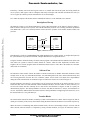
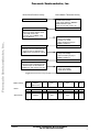
Order this document as AN496/D Freescale Semiconductor AN496/D Using MC683xx M-bus software to communicate between processor systems James Gilbert, Applications Group, High-Performance Products, Freescale Semiconductor, Inc. East Kilbride, Scotland. Freescale Semiconductor, Inc... Introduction M-bus is an I2C-compatible bus interface used in the 683xx family. It is a serial interface comprising two open-drain, bidirectional signals, namely serial clock (SCL) and serial data (SDA). Multiple devices can be connected directly to these open-drain lines, and indeed this is good reason for the widespread adoption of the bus as an efficient IC communication method in end-systems. A typical scenario would consist of a processor with an M-bus master controlling the data flow between several slaves, such as LCDs, real-time clocks, keypads, A/D converters and memories. Moreover, a built-in bus collision mechanism supports multiple M-bus masters as well as multiple slaves. The M-bus module of the 683xx is flexible enough to operate as either an M-bus master or a slave. This application note demonstrates control software for M-bus communication between two identical MC68307 systems, one configured with an M-bus master and the other an M-bus slave. Only a short piece of initialisation code needs to be changed to make the MC68307 code applicable to other 683xx devices with M-bus. Overview of M-bus Software Transfer Mechanism For full details of M-bus features, and a complete specification of the M-bus module, refer to the MC68307 User Manual. For the sake of clarity, a brief overview of the software control mechanism is provided here. The M-bus communication is on a byte-wide basis. The components of the hardware transfer protocol are a START condition, 8 data bits, an acknowledge bit and a STOP condition. Before starting a communication, an M-bus master should carry out a software check to ensure the bus is free, and therefore all other M-bus transfers are complete. Thereafter, the bus master initiates a transfer by software writing a START condition onto the bus. This is an indicator to all connected M-bus devices that this master is taking charge of the bus, and that the address of the targeted slave is to follow. For the 683xx Mbus master, writing the targeted slave address to the data register initiates the 8-bit transfer (MSB first). © Freescale Semiconductor, Inc., 2004. All rights reserved. If a system has two or more M-bus masters which poll the bus free and start a transfer at the same time, then the collision detection arbitration, throughout the transfer of the slave address transfer and subsequent data bytes, decides which device gets charge of the bus. If the 683xx M-bus loses arbitration in this way, it stops driving data onto the bus, to prevent data corruption. Furthermore, it switches automatically into slave mode pre-empting the alternate master addressing it as a slave. If interrupts are enabled, an interrupt is generated on the completion of that byte, and a status bit indicates arbitration lost as the interrupt source. The first data byte transmitted by the M-bus master is always the targeted slave address, with the least significant bit determining whether the slave remains ready to receive or transmit subsequent bytes. The addressed slave can then acknowledge the received byte, or not, depending upon the software protocol and acknowledge capability of the slave devices used. Each acknowledge is like a 9th data bit, asserted by the receiver as a handshake to successfully transmitted data. © Freescale Semiconductor, Inc., 2004. All rights reserved. 9/95 1995. All trademarks are recognised. Freescale Semiconductor, Inc. A block transfer comprising a series of data bytes (and acknowledges, if used) follows as commanded by the software protocol. The bus remains busy throughout the block, precluding all other masters from starting transfers. At the end of the block, the bus master relinquishes the bus by software placing a STOP condition onto the bus. Ultimately, the M-bus master is responsible for starting and stopping transfers, but the number of bytes transferred can be dictated by either the master or slave depending upon the desired software protocol. For example, a slave may acknowledge all bytes received until it saturates, at which point the master STOPs the block transfer. Alternatively, the slave receiver may acknowledge received bytes until the master transmitter dictates there are no more bytes to send. Indeed, both master and slave can be charged with controlling the transfer block. For instance, the software protocol may transfer a byte count as part of the communication, or use a fixed number of transfer bytes every time. Freescale Semiconductor, Inc... For the best choice in software control, transfers can adopt either a status polling method, or interrupts at the end of each byte. The interrupt option is most commonly used to minimise the time the processor is tied up with the transfers (overhead). If enabled, the interrupts are generated on the completion of each 9 bits (8 data bits plus an acknowledge). M-bus Master Mode Operation Using interrupts to transmit data to the addressed slave is straightforward. During the M-bus initialisation, the 683xx M-bus sets up master transmitter mode, sets the M-bus frequency, enables interrupts, provides an interrupt handler and STARTs the block transfer. The targeted slave address (with lsb = 1 for slave receiver mode) is transmitted by writing to the M-bus data register. On each subsequent end-of-byte interrupt, further data bytes are transmitted by writing data to the M-bus data register until the block is complete. On the interrupt at the end of the last byte the software STOPs the transfer. For receiving from the addressed slave, the initialisation is exactly the same. Remember that even if receiving, the first operation is to transmit the targeted slave address (except this time lsb = '0'). In the interrupt handler at the end of the slave address transmit byte, the transmit mode is changed to receive. Then, to initiate the first byte receive operation, the 683xx M-bus master software carries out a dummy read of the data register. No sensible data is read at this point, but it is the action of this read which starts the data receive. At the end of each received byte, the interrupt generated is used to read the data register again for valid data, and to start the next byte receive. This continues until the master receiver STOPs the block transfer. The receiver is always responsible for the generation of acknowledges. The 683xx M-bus receiver can be programmed to generate acknowledges automatically for each byte received if desired. Most slave transmitters take an acknowledge from the master receiver to mean that further bytes are desired. In fact, for some slave transmitters, it is necessary for the master receiver to acknowledge all received bytes (except the last one), to indicate that more data byte transmits are required. This is not a requirement of the 683xx M-bus slave. M-bus Slave Mode Operation Many of the principles discussed for the master operation also hold true for the slave 683xx M-bus. The main differences are that the M-bus is no longer controlling the transfer (STARTing and STOPping) or the provider of the M-bus clock, but is instead following what the master dictates. For slave operation, again initialise the M-bus frequency, M-bus slave address, interrupt handler and interrupt enable. As the first transfer is always the receipt of the slave address, slave receive mode should always be programmed initially. All target slave addresses which are transmitted by the master (first byte after START) are then checked against the programmed 683xx M-bus slave address for a match. When they match, an interrupt is generated (if enabled), and a status bit indicates the cause as M-bus addressed-as-slave (MAAS). On entering the corresponding interrupt handler, the software read/write status indicator is read to determine whether the slave is to receive or transmit subsequent bytes, and the transmit/receive mode set accordingly. If in transmit mode, the first data byte transmit is initiated by writing to the data register. If in receive mode, the first receive byte is 2 For More Information On This Product, Go to: www.freescale.com Freescale Semiconductor, Inc. initiated by a dummy read of the data register. There is no sensible data read at this point, but having started the receive process, data register reads in subsequent end-of-byte interrupts read valid data and initiate the next byte receive. Again, the software protocol determines the use of acknowledges. For a fuller description of the M-bus software and hardware features, see the MC68307 users’ manual. Description of Set-up Freescale Semiconductor, Inc... The hardware consists of two identical MC68307 systems connected together via the M-bus as shown in Figure 1. Both are master-mode processor systems, each with the MC68307 processor core executing instructions prefetched from ROM. This is not to be confused with the master and slave operation of the M-bus modules within each processor. 68307 System Mast er MBus SCL SDA 683 07 Syst em 5V 2. 2k 2. 2k SC L SD A Sl a ve MBus Figure 1 Hardware Setup Each MC68307 system has 128kB EPROM and 128kB SRAM and runs a debug monitor. A complete description of the system hardware is provided in AN490/D, “Multiple Bus Interfaces using the MC68307”. Using the monitor's download facility, an M-bus control program is downloaded into the SRAM of each board. The code allows one system to control its M-bus module as a master, while the other implements an M-bus slave. Together, the two software programs allow the MC68307 M-bus master to write data to the M-bus slave and later read it back for verification. Software Flow The MC68307 master M-bus controls the number of blocks transferred via START and STOP conditions. In this example, there are only two communication blocks, one transmitting data to the slave (master transmit block), and one receiving data back from the slave for verification (master receive block). The master/slave responsibilities during the master transmit block are outlined in Figure 2a and for the master receive block in Figure 3a. On these diagrams, note that for a given transfer byte, the end-of-byte interrupts on the master and slave occur at around the same time. The built-in M-bus transfer mechanism means it does not matter in which order they are serviced. The master and slave interrupt service order used in the flowcharts of Figures 2a and 3a is purely for demonstration purposes. The interrupt handlers are shown such that the data flow is always from transmitter to receiver. It should be understood that the master and slave interrupt handlers are happening at the same time, as are the transmit and receive of a particular byte. Transfer Blocks The master M-bus controls the number of data bytes within each transmit/receive block. Observe Figures 2b and 3b, which give a summary of the activity on the M-bus during the master transmit and master receive blocks respectively. When the master is transmitting data (master transmit block), the slave acknowledges all bytes received, and the master decides when the transfer is completed by setting a STOP condition; see Figure 2b. When the master is AN496/D For More Information On This Product, Go to: www.freescale.com 3 Freescale Semiconductor, Inc. receiving data (master receive block), it decides when the transfer is complete by stopping acknowledges on the last received byte, (thereby stopping the slave transmitting) and setting a STOP condition; see Figure 3b. Software Implementation The software used is shown in Software listing 1 and 2. Only the method of enabling the M-bus and interrupts at the start of the software listings is specific to the MC68307. Thereafter, the code is generic for any 683xx device with an M-bus module. Freescale Semiconductor, Inc... The 683xx M-bus slave software should always be set running before the master software, such that the prospective slave is initialised as a receiver before the master transmits the slave address. The software uses interrupts to control the byte transfers within each block. The M-bus master starts the transfer by transmitting the slave address. Thereafter interrupts are generated on both the master and slave M-bus to control the test. The M-bus hardware protocol does not care which order the interrupts are serviced by the master (transmitter or receiver) or slave (transmitter or receiver) at the end of each byte. Consider that the master is in charge of generating the SCL clocks to shift data out the transmitter and into the receiver, when a transmit/receive is initiated by writing/ reading the M-bus data register respectively. However, the clocks do not start until the slave has released the clock line on the bus by making its corresponding read/write of its M-bus data register. Therefore, both 683xx M-bus master and slave interrupts have to initiate the next data transfer. The slave frequency can be programmed as greater or less than that of the master. M-bus implements a clock synchronisation mechanism such that the clock with the shortest high time and longest low time dictates the opendrain clock. For example, if the programmed slave M-bus clock frequency is less than the master, the slave can stretch the clock as necessary. The number of transfer and receive blocks, and the number of data bytes within each block can be altered in the master software.The slave software remains the same throughout. If the user desires detailed crosschecks on the software flow, interrupt counts (for number of bytes transferred) or a flag passing mechanisms could be implemented. For simplicity this is not used in the example software. 4 For More Information On This Product, Go to: www.freescale.com Freescale Semiconductor, Inc. M-bus Slave Receiver Activity M-bus Master Transmitter Activity -Set slave Rx mode -Set master Tx mode -START block transfer -Write slave address to MBDR to initiate address Tx (66) (slave is to Rx data, so lsb = 0) -Rx slave address -Tx slave address Freescale Semiconductor, Inc... -Auto-Acknowledge address -Interrupt on Slave address match -Set Tx/Rx mode to Rx -Dummy read of MBDR, ready Rx 1st data byte -Interrupt at end of address Tx -Verify Acknowledge -Remain in Tx mode -Write 1st data byte (AA) to MBDR to initiate Tx -Tx data -Rx data -Auto-Acknowledge data -Interrupt at end of 1st data byte Rx -Read 1st byte of valid data from MBDR (AA), and ready for next Rx -Interrupt at end of 1st data byte Tx -Verify Acknowledge -Write 2nd data byte (55) to MBDR to initiate Tx -Tx data -Rx data -Auto-Acknowledge data -Interrupt at end of 2nd data byte Rx -Read 2nd byte of valid data from MBDR (55), and ready for next Rx -Interrupt at end of 2nd data byte Tx -Verify Acknowledge - STOP block transfer Figure 2a Master/Slave Responsibilities for the Master Transmit Block Master Activity Start Block M-bus Start Slave Activity Tx Slave Address (Slave to Rx) Tx 1st data byte Stop Block Tx 2nd data byte 66 Ack AA Ack Rx Slave Address Ack Rx 1st data byte Ack 55 Rx 2nd data byte Ack Stop Ack Figure 2b Summary of M-bus Activity for the Master Transmit Block AN496/D For More Information On This Product, Go to: www.freescale.com 5 Freescale Semiconductor, Inc. M-bus Slave Tranmitter Activit y M-bus M ast er Rece ive r A ct ivit y -Set s lave Rx m ode -S et mas ter T x m ode -S TAR T bl ock t ransf er -W rite sl av e addr es s to MBD R to in iti at e addr es s T x (67) (s lav e t o R x so lsb = 1) -Rx s lav e addr es s -T x s lav e addr es s Freescale Semiconductor, Inc... -Aut o- Ack nowledge addr ess -In ter rupt on Sl ave addr ess m atc h -S et T x/ Rx m ode t o T x -W rite 1st dat a by te (AA) to MBD R re ady to T x -I nt er rupt at end of addr es s T x - Ver ify Ack nowledge - Set Tx /R x mode to Rx - Du mmy r e ad of M BDR t o i ni tiate R x of 1st dat a by te (AA) -Tx d ata -Rx dat a -A uto- Ac know ledge dat a -I nt er rupt at end of 1s t data byt e R x - Re ad of M BDR r eady t o R x 2nd dat a by te (55) -In ter rupt at end of 1s t data byt e Tx -Ver ify Ac know ledge -W rite 2nd dat a by te (AA) to MBD R t o i ni tiate T x -Rx dat a -Tx d ata -N o Ac knowledge -I nt er rupt at end of 2nd by te Rx - STOP bl ock t ransf er -Int er rupt at end of 2nd dat a by te Tx - No Ack nowledge, s o end Tx - Sw itc h t o s lave Rx m ode ready f or nex t s lave addr ess Figure 3a Master/Slave Responsibilities for the Master Receive Block Master Activity Start Block Tx Slave Address (Slave to Tx) M-bus Start 67 Rx Slave Address Slave Activity Rx 1st data byte Ack Ack AA Ack Ack Tx 1st data byte Rx 2nd data byte 55 Tx 2nd data byte Figure 3b Summary of M-bus Activity for the Master Receive Block 6 For More Information On This Product, Go to: www.freescale.com No Ack No Ack Stop Block Stop Freescale Semiconductor, Inc. Freescale Semiconductor, Inc... Software Listing 1 - M-bus Master Software ********************************************************************** * FREESCALE 68307 IMBP TEST BOARD - MBUS * *====================================================================* * * * MODULE: MBM_INT.SRC DATE: 8/4/94 * * * * Developed by : Freescale * * HI-END Applications * * East Kilbride. * * * * NOTES: * * Master MBUS Routine using interrupts for a Master/Slave Test * * * * The number of bytes transmitted and received is completely * * controlled by the master. (i.e. When the slave is receiving data, * * it acknowledges all the time, and the master dictates the number of* * bytes to transfer. When the slave is transmitting, the master * * receiver acknowledges dictate whether the slave is to send further * * bytes or not.) * * * * The Master: * * 1) Writes out the slave chip address, and 2 slave data bytes. * * 2) Writes out the slave chip address, and reads 2 slave data bytes.* * 3) Verifies the data read back against that originally sent. * * * *============================================================================ * EXTERNAL REFERENCE DECLARATIONS *============================================================================ XREF SCR System Control Reg XREF PBCNT Port B Control Reg XREF PIVR Peripheral Interrupt Vector Reg XREF PICR Peripheral Interrupt Control Reg XREF MADR MBUS Address Reg XREF MFDR MBUS Freq Divider Reg XREF MBCR MBUS Control Reg XREF MBSR MBUS Status Reg XREF MBDR MBUS Data Reg *============================================================================ * Constants *============================================================================ UVECBASE EQU $100 User Vector Base MBUSVEC EQU UVECBASE+($D*4) MBUS vector location MBUSHAN EQU $15000 MBUS Interrupt Handler location S307_AD DRXCNT ATXCNT DTXCNT EQU EQU EQU EQU $66 $3 $1 $2 Slave 68307 MBus Address Data RECEIVE COUNT (2 + 1 Dummy) Address TRANSMIT COUNT Data TRANSMIT COUNT *============================================================================ * Main Program *============================================================================ ORG $10000 RANDOM LOCATION FOR ASSEMBLY AND.L #$FFFFFEFF,SCR Clear SCR bit 8, MBUS CLock Active MOVE.B #$40,PIVR Vector = #$40, Vector @ address $100 OR.W #$000D,PICR MBUS Interrupt level = 5 MOVE.L #MBUSHAN,MBUSVEC Set up MBUS Interrupt Handler OR.W #$0003,PBCNT Enable MBUS Lines BSR INIT_MBM Initialise MBus as master * WRITE TO SLAVE 68307 MBus * Write Chip Address, and Two bytes of data START BSR MBBUSY Poll the MBUS, wait till bus free MOVE.B MOVE.B MOVE.B MOVE.B MOVE.B MOVE.L #0,V_DRXCNT #ATXCNT,V_ATXCNT #DTXCNT,V_DTXCNT #1,V_WRITE #S307_AD,V_CHIPAD #S307_DATA,A0 Data RECEIVE COUNT Address TRANSMIT COUNT Data TRANSMIT COUNT Set Write to slave var = TRUE Slave 68307 Mbus receiver Address Pointer to stored data for transfer BSR WRITE1 Send out the Chip Address * READ FROM SLAVE 68307 MBus * Write Chip Address, and READ Two bytes of data AN496/D BSR MBBUSY Poll the MBUS, wait till bus free MOVE.B MOVE.B MOVE.B MOVE.B #DRXCNT,V_DRXCNT #ATXCNT,V_ATXCNT #0,V_DTXCNT #0,V_WRITE Data RECEIVE COUNT Address TRANSMIT COUNT Data TRANSMIT COUNT Set Write to slave var = FALSE For More Information On This Product, Go to: www.freescale.com 7 Freescale Semiconductor, Inc. MOVE.B OR.B MOVE.B MOVE.L #S307_AD,D6 #$01,D6 D6,V_CHIPAD #S307_DATA,A0 Alter chip address lsb for slave transmit and write to chip address variable Pointer to data for memory 1 BSR WRITE1 Send out the Chip Address MBBUSY FOREVER Poll the MBUS, wait till bus free Test complete & passed, loop forever * Test Complete BSR FOREVER BRA Freescale Semiconductor, Inc... ********************************************************************************* * MBUS SETUP/INITIALISATION ********************************************************************************* INIT_MBM MOVE.W #$2700,SR DISABLE INTERRUPTS BY SETTING TO LEVEL 7 MOVE.B #0,MBSR CLEAR INTERRUPT PEND, ARBITRATION LOST MOVE.B #$0C,MFDR SET FREQUENCY MOVE.B #$00,MBCR DISABLE AND RESET MBUS MOVE.B #$80,MBCR ENABLE MBUS RTS * NOTE - By not writing MADR, the 68307 MBUS slave address = 0 ********************************************************************************* * Poll the MBUS BUSY ********************************************************************************* MBBUSY BTST #5,MBSR TEST MBB BIT, BNE MBBUSY AND WAIT UNTIL IT IS CLEAR RTS ********************************************************************************* * GENERATION FIRST BYTE OF DATA TRANSFER ********************************************************************************* WRITE1 BTST #5,MBSR TEST MBB BIT, BNE WRITE1 AND WAIT UNTIL IT IS CLEAR TXSTART BSET #4,MBCR SET TRANSMIT MODE BSET #5,MBCR SET MASTER MODE (GENERATE START) BSET #6,MBCR Enable MBUS Interrupts MOVE.B (V_CHIPAD),MBDR TRANSMIT THE SLAVE CHIP ADDRESS MOVE.W #$2000,SR ENABLE INTERRUPTS BY SETTING TO LEVEL 0 MBFREE BTST BEQ RTS #5,MBSR MBFREE TEST MBB BIT, If bus is still free, wait until busy ********************************************************************************* * POST BYTE TRANSMISSION/RECEPTION SOFTWARE RESPONSE ********************************************************************************* ORG MBUSHAN Start of Interrupt Handler ISR BCLR #1,MBSR CLEAR THE MIF FLAG MOVE.L D0,-(A7) PUSH D0 REGISTER TO STACK MOVE.L D1,-(A7) PUSH D1 REGISTER TO STACK MOVE.L #0,D0 Clear general data reg MOVE.L #0,D1 Clear general data reg BTST BEQ #5,MBCR SLAVE CHECK THE MSTA FLAG BRANCH IF SLAVE MODE BTST BEQ #4,MBCR MASTRX CHECK THE MODE FLAG BRANCH IF RECEIVE MODE ********************************************************************************* * Master TRANSMIT caused Interrupt ********************************************************************************* MASTX BTST #0,MBSR CHECK ACK FROM RECEIVER, BNE ENDMASTX IF NO ACK, END TRANSMISSION TXADDR MOVE.B BEQ SUBQ.B V_ATXCNT,D1 TXDATA #1,V_ATXCNT CHECK Address TX COUNT If address already Complete go to data Decrement Address Tx Count TXDATA MOVE.B BEQ V_WRITE,D1 SETMASTRX Check if writing or reading slave If reading set to Master receive MOVE.B BEQ SUBQ.B MOVE.B BRA V_DTXCNT,D1 ENDMASTX #1,V_DTXCNT (A0)+,MBDR END CHECK Data TX COUNT IF NO MORE DATA THEN STOP BIT Reduce Tx Count Transmit next byte EXIT ENDMASTX BCLR BRA #5,MBCR END GENERATE STOP CONDITION EXIT SETMASTRX BCLR BCLR BSET #3,MBCR #4,MBCR #5,MBCR Enable TXAK Set master Receive Mode SET MASTER MODE (GENERATE START) 8 For More Information On This Product, Go to: www.freescale.com Freescale Semiconductor, Inc. ********************************************************************************* * Master RECEIVE ********************************************************************************* MASTRX SUBQ.B #1,V_DRXCNT Decrement receive count MOVE.B V_DRXCNT,D1 CMP.B #DRXCNT-1,D1 First byte read Check BNE NOTFIRST If not first, read and compare as usual MOVE.B MBDR,D0 If first, DUMMY read only to start Rx BRA END Freescale Semiconductor, Inc... NOTFIRST CMP.B BEQ SUBQ.B BNE #0,D1 ENMASR #1,D1 NXMAR LAMAR BSET BRA #3,MBCR NXMAR LAST SECOND, DISABLE ACK TRANSMITTING ENMASR BCLR #5,MBCR LAST ONE, GENERATE STOP SIGNAL NXMAR MOVE.B CMP.B BEQ MBDR,D0 (A0)+,D0 END READ DATA COMPARE WITH WRITTEN DATA If data as expected o.k. READERR BRA READERR Else ERROR loop forever. END MOVE.L MOVE.L RTE (A7)+,D1 (A7)+,D0 POP D1 REGISTER FROM STACK POP D0 REGISTER FROM STACK SLAVE NOP BRA SLAVE LAST BYTE TO BE READ CHECK LAST SECOND BYTE TO BE READ CHECK NOT LAST ONE OR LAST SECOND,SO BRANCH SLAVE OPERATION NOT IMPLEMENTED ********************************************************************************* * Buffers and Variables ********************************************************************************* V_WRITE DC.B $1 Slave write = True V_CHIPAD DC.B S307_AD Chip Address variable = Slave 307 Add V_DRXCNT DC.B DRXCNT Set up variables - Data Receive Count V_ATXCNT DC.B ATXCNT - Addr Transmit Count V_DTXCNT DC.B DTXCNT - Data Transmit Count S307_DATA DC.B $AA,$55 Chip 1 Data END AN496/D For More Information On This Product, Go to: www.freescale.com 9 Freescale Semiconductor, Inc. Software Listing 2 - M-bus Slave Software Freescale Semiconductor, Inc... ********************************************************************** * FREESCALE 68307 IMBP TEST BOARD - MBUS * *====================================================================* * * * MODULE: MBS_INT.SRC DATE: 8/4/94 * * * * Developed by : Freescale * * HI-END Applications * * East Kilbride. * * * * NOTES: * * Slave MBUS Routine using interrupts for a Master/Slave Test * * * * The number of bytes transmitted and received is completely * * controlled by the master. (i.e. When the slave is receiving data, * * it acknowledges all the time, and the master dictates the number of* * bytes to transfer. When the slave is transmitting, the master * * receiver acknowledges dictate whether the slave is to send further * * bytes or not.) * * * * The Slave: * * 1) Recognises its slave chip address, and receives 2 data bytes. * * 2) Recognises its slave chip address, and transmits the 2 bytes. * * * *============================================================================ * EXTERNAL REFERENCE DECLARATIONS *============================================================================ XREF SCR System Control Reg XREF PBCNT Port B Control Reg XREF PIVR Peripheral Interrupt Vector Reg XREF PICR Peripheral Interrupt Control Reg XREF MADR MBUS Address Reg XREF MFDR MBUS Freq Divider Reg XREF MBCR MBUS Control Reg XREF MBSR MBUS Status Reg XREF MBDR MBUS Data Reg *============================================================================ * Constants *============================================================================ UVECBASE EQU $100 User Vector Base MBUSVEC EQU UVECBASE+($D*4) MBUS vector location MBUSHAN EQU $15000 MBUS Interrupt Handler location S307_AD EQU $66 Slave 68307 MBus Address *============================================================================ * Main Program *============================================================================ ORG $10000 RANDOM LOCATION FOR ASSEMBLY AND.L #$FFFFFEFF,SCR Clear SCR bit 8, MBUS CLock Active MOVE.B #$40,PIVR Vector = #$40, Vector @ address $100 OR.W #$000D,PICR MBUS Interrupt level = 5 MOVE.L #MBUSHAN,MBUSVEC Set up MBUS Interrupt Handler OR.W #$0003,PBCNT Enable MBUS Lines BSR INIT_MBS Initialise MBus as slave FINISH BRA FINISH Loop forever ********************************************************************************* * MBUS SETUP/INITIALISATION ********************************************************************************* INIT_MBS MOVE.W #$2700,SR DISABLE INTERRUPTS BY SETTING TO LEVEL 7 MOVE.B #0,MBSR CLEAR INTERRUPT PEND, ARBITRATION LOST MOVE.B #$10,MFDR Set FREQUENCY MOVE.B #S307_AD,MADR Set MBUS slave address MOVE.B #$00,MBCR DISABLE AND RESET MBUS OR.B #$C0,MBCR ENABLE MBUS, Ints, TXAK MOVE.W #$2300,SR Enable INTS BY SETTING TO LEVEL 3 RTS ********************************************************************************* * Poll the MBUS BUSY ********************************************************************************* MBBUSY BTST #5,MBSR TEST MBB BIT, BNE MBBUSY AND WAIT UNTIL IT IS CLEAR RTS 10 For More Information On This Product, Go to: www.freescale.com Freescale Semiconductor, Inc. ********************************************************************************* * POST BYTE TRANSMISSION/RECEPTION SOFTWARE RESPONSE ********************************************************************************* ORG MBUSHAN Start of Interrupt Handler ISR BCLR #1,MBSR CLEAR THE MIF FLAG MOVE.L D0,-(A7) PUSH D0 REGISTER TO STACK MOVE.L D1,-(A7) PUSH D1 REGISTER TO STACK MOVE.L #0,D0 Clear general data reg MOVE.L #0,D1 Clear general data reg * Interrupt Counter ADDQ.L #1,D3 (Not used, simply monitor) MASTER BTST BEQ #5,MBCR SLAVE CHECK THE MSTA FLAG BRANCH IF SLAVE MODE BRA MASTER Master not implemented, so error Freescale Semiconductor, Inc... ********************************************************************************* SLAVE MOVE.B MBSR,D6 Read MBSR BTST.B #6,D6 Is it slave address byte? BEQ SLAVE_DATA If not, then data ********************************************************************************* * Addressed as SLAVE ********************************************************************************* SLAVE_ADD BTST #2,D6 Read SRW to verify slave Tx or Rx BEQ INIT_SRX If Rx, initialise SLAVE receive count INIT_STX OR.B MOVE.L MOVE.B BRA #$10,MBCR #DATABUF,A0 (A0)+,MBDR END_SLAVE Set transmit mode Pointer to data storage buffer First data byte transmit INIT_SRX AND.B MOVE.L MOVE.B BRA #$E7,MBCR #DATABUF,A0 MBDR,D0 END_SLAVE Set receive mode and TXAK Pointer to data storage buffer Start receive via Dummy byte read ********************************************************************************* * Slave Data ********************************************************************************* SLAVE_DATA BTST #4,MBCR Read Tx or Rx mode BEQ SRX_DATA ********************************************************************************* * Post Slave data Transmit Control ********************************************************************************* STX_DATA BTST #0,MBSR CHECK ACK FROM RECEIVER, BEQ NXT_TX IF ACK, THEN TX NEXT DATA BYTE NXT_TX AND.B MOVE.B BRA #$EF,MBCR MBDR,D0 END_SLAVE TX complete so swap to Rx Dummy read to free bus (SCL) Finish and await Master MOVE.B BRA (A0)+,MBDR END_SLAVE Tx next data byte EXIT ********************************************************************************* * Post Slave data Receive Control ********************************************************************************* SRX_DATA MOVE.B MBDR,D0 READ DATA MOVE.B D0,(A0)+ Store data in next data buffer location END_SLAVE MOVE.L MOVE.L RTE (A7)+,D1 (A7)+,D0 POP D1 REGISTER FROM STACK POP D0 REGISTER FROM STACK ********************************************************************************* * Buffers and Variables ********************************************************************************* DATABUF DS.B 0 Slave data buffer between Rx and Tx END AN496/D For More Information On This Product, Go to: www.freescale.com 11 Freescale Semiconductor, Inc. How to Reach Us: Home Page: www.freescale.com Freescale Semiconductor, Inc... E-mail: [email protected] USA/Europe or Locations Not Listed: Freescale Semiconductor Technical Information Center, CH370 1300 N. Alma School Road Chandler, Arizona 85224 +1-800-521-6274 or +1-480-768-2130 [email protected] Europe, Middle East, and Africa: Freescale Halbleiter Deutschland GmbH Technical Information Center Schatzbogen 7 81829 Muenchen, Germany +44 1296 380 456 (English) +46 8 52200080 (English) +49 89 92103 559 (German) +33 1 69 35 48 48 (French) [email protected] Japan: Freescale Semiconductor Japan Ltd. Headquarters ARCO Tower 15F 1-8-1, Shimo-Meguro, Meguro-ku, Tokyo 153-0064 Japan 0120 191014 or +81 3 5437 9125 [email protected] Asia/Pacific: Freescale Semiconductor Hong Kong Ltd. Technical Information Center 2 Dai King Street Tai Po Industrial Estate Tai Po, N.T., Hong Kong +800 2666 8080 [email protected] For Literature Requests Only: Freescale Semiconductor Literature Distribution Center P.O. Box 5405 Denver, Colorado 80217 1-800-441-2447 or 303-675-2140 Fax: 303-675-2150 [email protected] Information in this document is provided solely to enable system and software implementers to use Freescale Semiconductor products. There are no express or implied copyright licenses granted hereunder to design or fabricate any integrated circuits or integrated circuits based on the information in this document. Freescale Semiconductor reserves the right to make changes without further notice to any products herein. Freescale Semiconductor makes no warranty, representation or guarantee regarding the suitability of its products for any particular purpose, nor does Freescale Semiconductor assume any liability arising out of the application or use of any product or circuit, and specifically disclaims any and all liability, including without limitation consequential or incidental damages. “Typical” parameters which may be provided in Freescale Semiconductor data sheets and/or specifications can and do vary in different applications and actual performance may vary over time. All operating parameters, including “Typicals” must be validated for each customer application by customer’s technical experts. Freescale Semiconductor does not convey any license under its patent rights nor the rights of others. Freescale Semiconductor products are not designed, intended, or authorized for use as components in systems intended for surgical implant into the body, or other applications intended to support or sustain life, or for any other application in which the failure of the Freescale Semiconductor product could create a situation where personal injury or death may occur. Should Buyer purchase or use Freescale Semiconductor products for any such unintended or unauthorized application, Buyer shall indemnify and hold Freescale Semiconductor and its officers, employees, subsidiaries, affiliates, and distributors harmless against all claims, costs, damages, and expenses, and reasonable attorney fees arising out of, directly or indirectly, any claim of personal injury or death associated with such unintended or unauthorized use, even if such claim alleges that Freescale Semiconductor was negligent regarding the design or manufacture of the part.