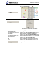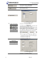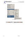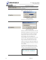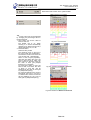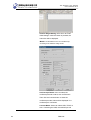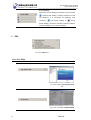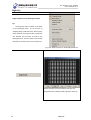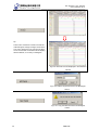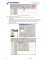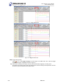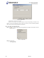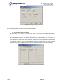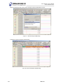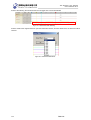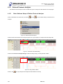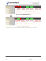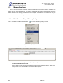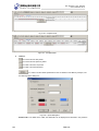
1
The Zeroplus Logic Analyzer
User’s Manual V3.12
1
FM07I4A
The Zeroplus Logic Analyzer
User’s Manual V3.12
Index
1
Features of Zeroplus Logic Analyzer ................................................................................................................ 5
1.1
Package Contents................................................................................................................................... 6
1.2
Introduction ............................................................................................................................................. 8
1.3
Hardware Specifications ....................................................................................................................... 12
1.4
System Requirements........................................................................................................................... 15
1.4.1
Operating System Requirements ..................................................................................................... 15
1.4.2
Hardware System Requirements ..................................................................................................... 15
1.5
2
Device Maintenance and Safety ........................................................................................................... 16
Installation ...................................................................................................................................................... 18
2.1
Software Installation.............................................................................................................................. 19
2.2
Hardware Installation ............................................................................................................................ 21
2.3 Tips and Advice .......................................................................................................................................... 23
3
User Interface................................................................................................................................................. 24
3.1
Menu & Tool Bars.................................................................................................................................. 27
3.2
Find Data Value .................................................................................................................................... 77
3.3
Statistics Feature .................................................................................................................................. 81
3.4
Customize Interface .............................................................................................................................. 84
3.4.1
Modify Waveform Display Mode....................................................................................................... 85
3.4.2
Modify Ruler Mode ........................................................................................................................... 86
3.4.3
Modify Waveform Height & Correlated Setting................................................................................. 87
3.5
Auto Save ............................................................................................................................................. 90
3.6
Color Setting ......................................................................................................................................... 91
3.6.1 Modify Workaround Color ................................................................................................................... 93
3.6.2 Modify Waveform Color ...................................................................................................................... 94
3.7 The Flow of Software Operation.................................................................................................................... 96
4
2
Introduction to Logic Analysis ......................................................................................................................... 97
4.1
Logic Analysis ....................................................................................................................................... 98
4.2
Bus Logic Analysis ...............................................................................................................................110
4.3
Plug Analysis .......................................................................................................................................113
4.4
Bus Packet List ....................................................................................................................................115
4.5
Bus Analysis ....................................................................................................................................... 122
4.5.1
Bus Analysis................................................................................................................................... 123
4.5.2
I2C Analysis ................................................................................................................................... 126
4.5.3
UART Analysis ............................................................................................................................... 132
4.5.4
SPI Analysis ................................................................................................................................... 137
FM07I4A
The Zeroplus Logic Analyzer
User’s Manual V3.12
4.5.5
1-WIRE Analysis ............................................................................................................................ 142
4.5.6
HDQ Analysis ................................................................................................................................. 152
4.5.7
CAN 2.0B Analysis ......................................................................................................................... 159
4.6
Compression....................................................................................................................................... 169
4.6.1
4.7
Software Basic Setup of Compression........................................................................................... 169
Signal Filter and Filter Delay............................................................................................................... 171
4.7.1
4.8
Basic Setup of Signal Filter and Filter Delay .................................................................................. 171
Noise Filter.......................................................................................................................................... 176
4.8.1
4.9
Basic Software Setup of Noise Filter.............................................................................................. 176
Data Contrast...................................................................................................................................... 178
4.9.1
4.10
Basic Software Setup of Data Contrast .......................................................................................... 178
Refresh Protocol Analyzer .................................................................................................................. 181
4.10.1
4.11
Memory Analyzer ................................................................................................................................ 183
4.11.1
4.12
5
6
7
3
Basic Software Setup of Memory Analyzer................................................................................ 183
Multi-stacked Logic Analyzer Settings................................................................................................. 187
4.12.1
4.13
Basic Software Setup of Refresh Protocol Analyzer.................................................................. 181
Basic Software Setup of Multi-stacked Logic Analyzer Settings ................................................ 187
DSO-stacked Settings......................................................................................................................... 189
Troubleshooting............................................................................................................................................ 198
5.1
Installation Troubleshooting ................................................................................................................ 199
5.2
Software Troubleshooting ................................................................................................................... 200
5.3
Hardware Troubleshooting.................................................................................................................. 201
FAQ .............................................................................................................................................................. 202
6.1
Hardware ............................................................................................................................................ 203
6.2
Software.............................................................................................................................................. 205
6.3
Registration......................................................................................................................................... 209
6.4
Technical Information .......................................................................................................................... 210
6.5
Others ......................................................................................................................................................211
Appendix ...................................................................................................................................................... 212
7.1
Hot Keys ............................................................................................................................................. 213
7.2
Contact Us .......................................................................................................................................... 216
FM07I4A
The Zeroplus Logic Analyzer
User’s Manual V3.12
Preface
This Quick Start Guide is designed to help new and intermediate users navigate and perform common tasks
with the Zeroplus Logic Analyzer. Despite its simple packaging and interface, the Logic Analyzer is a sophisticated
measurement and analysis tool. It is also a highly sensitive electrical current sensing device. Users must carefully
read instructions and procedures pertaining to installation and operation. Any instrument connected to the unit
should be properly grounded. A pair of anti-static gloves is strongly recommended when performing a task with the
device. To ensure accuracy and consistency of output data, use of the bundled components is strongly
recommended.
Users’ opinions are very important to Zeroplus. Please contact our engineering team by telephone, fax or email
with your questions or feedback. Thank you for choosing the Zeroplus Logic Analyzer.
Notice: We will not have additional notice for you when there is any modification to the User Manual. If there is any
unconformity caused by software upgrade, users should take the software as the standard.
4
FM07I4A
The Zeroplus Logic Analyzer
User’s Manual V3.12
1 Features of Zeroplus Logic
Analyzer
5
1.1
Package Contents
1.2
Introduction
1.3
Hardware Specifications
1.4
System Requirements
1.5
Device Maintenance and Safety
FM07I4A
The Zeroplus Logic Analyzer
User’s Manual V3.12
Objective
In this chapter, users will learn about the package contents, description, hardware specifications, system
requirements and safety issues of the Zeroplus Logic Analyzer. Although this chapter is purely informative, we
highly recommend reading this carefully to ensure safety and accuracy when performing any operation with the
Zeroplus Logic Analyzer.
1.1
Package Contents
Verify the package contents before discarding packing materials. The following components should be
included with your product. For assistance, please contact our nearest distributor.
Table 1-1: Accessories List
LAPModels
16032U
Logic
Analyzer
16-Pin
Testing
Cable
8-Pin
Testing
Cable
Probe
USB
Cable
Quick
Start
Guide
Driver
CD**
1-Pin
Testing
Cable
(White)
2-Pin
Testing
Cable
(Black)
Models
Logic
Analyzer
16-Pin
Testing
Cable
8-Pin
Testing
Cable
Probe
USB
Cable
Quick
Start
Guide
Driver
CD**
6
LAP16064U
LAP16128U
LAP32128U-A
LAP321000U-A
LAP322000U-A
1
1
1
1
1
1
0
0
0
1
1
1
2
2
2
2
2
2
2
20
20
36
36
36
1
1
1
1
1
1
0
1
1
1
1
1
1
1
1
1
1
1
1
1
1
1
1
1
1
1
1
1
1
1
LAP-C
(16032)
LAP-C
(16064)
LAP-C
(16128)
LAP-C
(162000)
LAP-C
(32128)
LAP-C
(321000)
LAP-C
(322000)
1
1
1
1
1
1
1
0
0
0
0
1
1
1
2
2
2
2
2
2
2
2
20
20
20
36
36
36
1
1
1
1
1
1
1
0
1
1
1
1
1
1
1
1
1
1
1
1
1
FM07I4A
The Zeroplus Logic Analyzer
User’s Manual V3.12
1-Pin
Testing
Cable
(White)
2-Pin
Testing
Cable
(Black)
1
1
1
1
1
1
1
1
1
1
1
1
1
1
* This Driver CD contains multilingual software interface program as well as multilingual User Manual.
* The following are accessories of LAP-C Series, which are the same with that of LAP-A.
16-Pin x 1
8-Pin x 2
Fig. 1-1: Logic Analyzer
Fig. 1-3: Probe
(varied depending on models)
Fig. 1-4: USB Cable
Fig. 1-5: Quick Start Guide
Fig. 1-6: Driver CD
Fig. 1-7: 1-Pin External Clock Cable
(White)
7
Fig. 1-2: Testing Cable
Fig. 1-8: 2-Pin Ground Cable
(Black)
FM07I4A
The Zeroplus Logic Analyzer
User’s Manual V3.12
1.2
Introduction
1. Zeroplus Logic Analyzer models LAP-16032U, LAP-16064U, LAP-16128U, LAP-32128U-A, LAP-321000U-A,
and LAP-322000U-A, all share the same external features as illustrated in the following figures.
Fig. 1-9 A view of the Zeroplus Logic Analyzer LAP-A Series. See Fig 1-12 for detailed information on the Signal
Connectors.
Fig. 1-10 Side view of Zeroplus Logic Analyzer, which draws its power from the USB connection.
Port A: A0 ~ A7
Port B: B0 ~ B7
Port C: C0 ~ C7
Port D: D0 ~ D7
For signal transmission to
active other instruments
For the External Clock
connection.
For extended modules or
devices not designated to
be analyzed.
For grounding test circuits
Fig. 1-11 Rear view of Zeroplus Logic Analyzer LAP-A Series
8
FM07I4A
The Zeroplus Logic Analyzer
User’s Manual V3.12
2. Zeroplus Logic Analyzer LAP-C Series share the same external features as illustrated in the following figures.
Fig. 1-12: A View of the Zeroplus Logic Analyzer LAP-C Series. See Fig 1-11 for detailed information on the Signal
Connectors
Fig. 1-13: Side View of the Zeroplus Logic Analyzer; the power of the Logic Analyzer is drawn from the USB
connection.
Port A: A0 ~ A7
Port B: B0 ~ B7
Port C: C0 ~ C7
Port D: D0 ~ D7
For transmitting signals to
activate other instruments
For connecting the
External Clock
For external modules or devices not
designated to be analyzed
For grounding test circuits
Fig. 1.14 Side View of the Zeroplus Logic Analyzer LAP-C Series
9
FM07I4A
The Zeroplus Logic Analyzer
User’s Manual V3.12
Table 1-2A: List of Functional Pins in Each Model
Models
LAP16032U
LAP16064U
Port A
( A0~A7)
Port B
( B0~B7)
Port C
( C0~C7)
Port D
( D0~D7)
R_O
T_O
S_O
CLK
GND
LAP16128U
LAP32128U-A
LAP32100U-A
LAP322000U-A
√
√
√
√
√
√
X
√
√
X
√
√
√
√
√
√
√
√
√
√
√
√
√
√
√
√
√
Table 1-2B: List of Functional Pins in Each Model
Models
LAP-C
(16032)
LAP-C
(16064)
Port A
( A0~A7)
Port B
( B0~B7)
Port C
( C0~C7)
Port D
( D0~D7)
R_O
T_O
S_O
CLK
GND
VDD
IOA
IOB
IOC
GND
LAP-C
(16128)
LAP-C
(162000)
LAP-C
(32128)
LAP-C
(321000)
LAP-C
(322000)
√
√
√
√
√
√
X
√
√
X
√
√
√
√
√
√
√
√
√
√
√
√
√
√
√
√
√
√
√
√
√
√
√
√
√
√
√
√
√
√
√
√
Table1-3: Definitions and Functions of Pins for All Models
CLK
Clock
GND
Ground
Connect a given external module to be analyzed.
Two pins used for grounding the Logic Analyzer with a given
external module to be analyzed.
Table1-4: Definitions and Functions of Pins for Advanced Models (1)
10
R_O
Read (Out)
T_O
Trigger (Out)
S_O
Start (Out)
When the Logic Analyzer is about to upload data from the
memory to the PC, the R_O will send a Rising Edge signal
of DC3.3V. When the upload is finished, a Falling Edge
signal is sent.
When a trigger condition is established, the T_O will send a
Rising Edge signal of DC3.3V. When the memory is full, a
Falling Edge signal is sent.
When a user initiates a sampling task by clicking the RUN
icon in the window or clicking the START button on the
device, the S_O will send a Rising Edge signal of DC3.3V.
FM07I4A
The Zeroplus Logic Analyzer
User’s Manual V3.12
When the Logic Analyzer finishes uploading, a Falling Edge
signal is sent.
Table1-5: Definitions and Functions of Pins for Advanced Models (2)
11
VDD
Voltage Drain
(Semiconductor)
IOA
Ext. I/O Module A
IOB
IOC
GND
Ext. I/O Module B
Ext. I/O Module C
Ground
Provide +3.3 V for external modules by draining
voltage from the Logic Analyzer.
Transmit signals between an external model or
device and the Logic Analyzer.
Same as IOA.
Same as IOA.
Ground external devices in sequence.
FM07I4A
The Zeroplus Logic Analyzer
User’s Manual V3.12
1.3
Hardware Specifications
Table 1-6A: Hardware Specifications of LAP-A Series
Items\Type
LAP16032U
LAP16064U
LAP16128U
LAP32128U-A
LAP321000U-A
Interface
USB 2.0 (1.1)
Operating System
Windows 2000/ Windows XP/ Windows Vista/ Windows 7
Power Supply
USB 1.1 (USB 2.0 Recommended)
16
Channels
Sampling
Rate
32
Internal
Clock Rate
(asynchronous)
100Hz ~ 100MHz
100Hz ~ 200MHz
Max
External
Clock
(synchronous)
Max 75MHz
Max 100MHz
75MHz
Bandwidth
Memory
Memory
Trigger
Memory
Depth (Per
Channel)
Trigger
Channel
Trigger
Condition
Pre-Trigger/
Post-Trigger
512K Bits
1M Bits
4M Bits
4M Bits
32M Bits
64M Bits
32K Bits
64K Bits
128K
Bits
128K Bits
1M Bits
2M Bits
16 Channels
32 Channels
Pattern/Edge
Yes
Trigger Level
1 Level
Trigger Count
1~65535
Threshold
Working
Voltage
-6V~+6V
Voltage
Accuracy
±0.1V
I2C
Free
UART
Free
Protocol
SPI
Free
Analyzer
1-WIRE
Free
(Keep
CAN 2.0B
Free
Increasing)
HDQ
Software
7-SEGMEN
T LED
Operating
Interface
Language
Time Base
Range
Vertical
Sizing
Function
Compression
12
LAP-322000U-A
Option
Free
Free
Chinese(Si)/ Chinese(Tr)/ English
5ps~10Ms
1~5.5
Max
8Mbits
Max
16Mbits
Max
32Mbits
Max
32Mbits
Max
255Mbits
FM07I4A
Max 512Mbits
The Zeroplus Logic Analyzer
User’s Manual V3.12
Waveform
Width
Display
Yes
Trigger Page
1~8192Page
Pulse Width
Trigger
Free
Double Mode
Yes
Option
Trigger Mark
Latch
Function
Data
Contrast
Multi-stacked
Logic
Analyzer
Settings
Protocol
Analyzer
Trigger
Free
Option
Option
Option
Option
Free
Free
Option
Option
Option
Option
Free
Free
No
No
No
Yes
Yes
Yes
Option
Free
FCC/CE/WEEE/RoHS
Safety Certification
Table 1-6B: Hardware Specifications of LAP-C Series
Items\Type
LAP-C
(16032)
LAP-C
(16064)
LAP-C
(16128)
LAP-C
(32128)
LAP-C
(321000)
Interface
USB 2.0 (1.1)
Operating System
Windows 2000/ Windows XP/ Windows Vista/ Windows 7
Power Supply
USB 1.1 (USB 2.0 Recommended)
16
Channels
Sampling
Rate
Internal
Clock Rate
(asynchronous)
100Hz ~ 100MHz
100Hz ~ 200MHz
Max
External
Clock
(synchronous)
Max 75MHz
Max 100MHz
Memory
Memory
Trigger
Threshold
Memory
Depth (Per
Channel)
Trigger
Channel
Trigger
Condition
Pre-Trigger/
Post-Trigger
LAP-C
(322000)
32
75MHz
Bandwidth
13
LAP-C
(162000)
512K Bits
1M Bits
4M Bits
64M Bits
4M Bits
32M Bits
64M Bits
32K Bits
64K Bits
128K Bits
2M Bits
128K Bits
1M Bits
2M Bits
16 Channels
32 Channels
Pattern/Edge
Yes
Trigger Level
1 Level
Trigger Count
1~65535
Working
Voltage
-6V~+6V
FM07I4A
The Zeroplus Logic Analyzer
User’s Manual V3.12
Accuracy
±0.1V
I2C
Free
UART
Free
Protocol
SPI
Free
Analyzer
1-WIRE
Free
(Keep
CAN 2.0B
Free
Increasing)
HDQ
Voltage
Option
7-SEGMEN
T LED
Operating
Interface
Language
Time Base
Range
Vertical
Sizing
Compression
Free
Chinese(Si)/ Chinese(Tr)/ English
5ps~10Ms
1~5.5
Max
8Mbits
Max
16Mbits
Max
32Mbits
Max
512Mbits
Max
32Mbits
Waveform
Width
Display
Yes
Trigger Page
1~8192Page
Pulse Width
Trigger
Free
Software
Double Mode
Function
Trigger Mark
Latch
Function
Data
Contrast
Multi-stacked
Logic
Analyzer
Settings
Protocol
Analyzer
Trigger
Safety Certification
14
Free
No
Max
255Mbits
Max
512Mbits
Yes
Option
Free
Option
Option
Free
Option
Free
Option
Free
Option
Free
No
Free
Yes
Option
Free
FCC/CE/WEEE/RoHS
FM07I4A
The Zeroplus Logic Analyzer
User’s Manual V3.12
1.4
System Requirements
This section discusses basic operating system and hardware requirements for the Logic Analyzer. Software and
hardware capability may vary along with PC configuration. This manual assumes that one of supported operating
systems(listed below) is properly installed.
1.4.1 Operating System Requirements
Support
Operating System
Name
z Windows 2000
(Professional, Server Family)
z Windows XP
(Home, Professional Editions 32-Bit
version)
z Windows VISTA
(32-Bit and 64-Bit version)
z Windows 7
(32-Bit and 64-Bit version)
Non-support
z Windows NT 4.0 (Workstation & Server,
Service Pack 6)
z Windows Server 2003
1.4.2 Hardware System Requirements
Hardware Name
Lowest Configuration
Recommended Configuration
CPU
166 MHz
900 MHz
Memory
64MB
256MB
Display Device
Hard Drive
USB
15
VGA Display Capability with
1024x768 resolution or higher.
VGA Display Capability with
1024x768 resolution or higher.
At least 100MB available space
At least 100MB available space
USB1.1 supported
USB2.0 recommended
FM07I4A
The Zeroplus Logic Analyzer
User’s Manual V3.12
1.5
Device Maintenance and Safety
Follow these instructions for proper operation and storage of the Logic Analyzer.
Table1-7: General Advice
Cautions
•
•
•
•
Do not place heavy objects on the Zeroplus Logic Analyzer.
Avoid hard impacts and rough handling.
Protect the Logic Analyzer from static discharge.
Do not disassemble the Zeroplus Logic Analyzer; this will void the
warranty and could affect its operation.
•
•
Use a soft, damp cloth with a mild detergent to clean.
Do not spray any liquid on the Zeroplus Logic Analyzer or
immerse it in any liquid.
Do not use harsh chemicals or cleaners containing substances
such as benzene, toluene, xylene or acetone.
Cleaning
•
Table1-8: Electrical Specifications(LAP-A Series & LAP-C Series)
Items
Minimum
Working Voltage
DC 4.5 V
Current at Rest
Current at Work
Power at Rest
Power at Work
Error in Phase Off*
Vinput of Testing Channel
DC -30V
VReference
DC -6V
Input Resistance
Working Temperature
5°C
Storage Temperature
-40°C
Typical
DC 5.0 V
Maximum
DC 5.5 V
200 mA
400 mA
1W
2W
1.5 nS
DC 30 V
DC 6 V
500K /10pF
70°C
80°C
* Refer to the User Manual for error analysis calculation.
16
FM07I4A
The Zeroplus Logic Analyzer
User’s Manual V3.12
Table1-9: Operating Environment
•
•
•
•
•
Avoid direct sunlight
Use in a dust free, non-conductive environment (see Note)
Relative Humidity: < 80%
Altitude: < 2000m
Temperature: 0 ~ 40 Degrees C
This is a Class A product which may cause radio interference in a
domestic environment.
Note: EN 61010-1:2001 specify degrees of pollution and their
requirements. Logic Analyzer falls under Level 2.
WARNING
Pollution refers to ‘addition of foreign matter, solid, liquid or gaseous
(ionized gases), which may produce a reduction of dielectric strength
or surface resistivity’.
Pollution Degree 1: No pollution or only dry, non-conductive pollution
occurs. This pollution has no effect.
Pollution Degree 2: Normally only non-conductive pollution occurs.
Occasionally, however, temporary conductivity caused by the
condensation must be expected.
Pollution Degree 3: Conductive pollution occurs or dry,
non-conductive pollution which becomes conductive due to the
condensation occurs. In such conditions, the equipment is normally
protected against exposure to direct sunlight, precipitation and wind,
but neither temperature nor humidity is controlled.
Storage
Environment
Relative Humidity: < 80%
Temperature: 0 ~ 50 Degrees C
Conclusion
After reading this section, users should have a basic grasp of the Logic Analyzer. A complete understanding of
the section, Device Maintenance and Safety, is a critical prerequisite of any further operation as presented in the
User Manual.
17
FM07I4A
The Zeroplus Logic Analyzer
User’s Manual V3.12
2 Installation
18
2.1
Software Installation
2.2
Hardware Installation
2.3
Tips and Advice
FM07I4A
The Zeroplus Logic Analyzer
User’s Manual V3.12
Objective
This chapter describes the installation of the Logic Analyzer hardware and software. Software installation steps
must be followed precisely to ensure successful installation.
2.1
Software Installation
In this section, users will learn how to install the software and drivers. As with proper installation of many USB
devices, the Logic Analyzer application and driver software must be installed prior to the connection of the hardware.
The following steps illustrate an installation of a Zeroplus LAP-C V3.11 Logic Analyzer. The other twelve models
mentioned in Chapter 1 would follow identical procedures.
Step 1. Insert the driver CD-ROM in the PC CD drive.
Step 2. Execute the installation program. Go to the START menu, click START, Run, Browse in sequence,
select Setup.exe file in the appropriate model folder and then click OK. It is recommended that all other
programs are closed while the installation proceeds.
Step 3. Choose the Application Setup.
Step 4. Click Next to proceed with the Install Wizard.
Step 5. Select “I accept the terms of the license agreement”, and click Next.
Step 6. Enter User and Company names.
Step 7. Choose the setup type. We recommend Complete for most users.
Step 8. Click Install to confirm settings and begin the actual installation.
Step 9. Click Finish to complete the installation.
19
FM07I4A
The Zeroplus Logic Analyzer
User’s Manual V3.12
20
FM07I4A
The Zeroplus Logic Analyzer
User’s Manual V3.12
2.2
Hardware Installation
Hardware installation simply involves in connecting the Logic Analyzer to your computer with the included USB
Cable as shown in Figures 2-4 and 2-5.
1. Plug the fixed end of the cables into the
LA (Fig. 2-1).
Fig. 2-1
2. Plug the loose ends into the connectors
on the circuit board to be analyzed (Fig.
2-2).
Note: The following sequence must be
observed when connecting the
connectors into the circuit board: A0 =
Brown, A1 = Red, A2 = Orange, A3 =
Yellow, A4 = Green, A5 = Blue, A6 =
Purple and A7 = Gray.
Fig. 2-2
3. The circuit board must be grounded to
the Logic Analyzer with the black
Ground Cable (Fig. 2-3).
Fig. 2-3
4. Plug the square end of the USB cable
into the Logic Analyzer (Fig. 2-4).
Fig. 2-4
5. Plug the thin end into the computer (Fig.
2-5).
Fig. 2-5
21
FM07I4A
The Zeroplus Logic Analyzer
User’s Manual V3.12
At this point, the computer should be able to detect the Logic Analyzer and finalize the installation for hardware
connection. For further information, refer to the Troubleshooting and Frequently Asked Questions (FAQ) chapters in
the User Manual.
Fig. 2-6: An Assembly of Laptop, Logic Analyzer and Testing Board of LAP-C Series
Fig.2-7 An Assembly of Laptop, Logic Analyzer and Testing Board of LAP-A Series
22
FM07I4A
The Zeroplus Logic Analyzer
User’s Manual V3.12
2.3
Tips and Advice
1.
When testing a circuit board, make sure that the internal sampling frequency (within the Logic Analyzer) is at
least four times higher than the external board frequency.
2.
If the signal connector does not work well with the pins on the test board, try to use the supplied probes.
Fig. 2-8: Probes Supplied with Zeroplus
3. Usages of probes
3-1. Take the loose end of the cable and
insert it into the clip (Fig. 2-9).
Fig. 2-9
3-2. Compress the probe as shown to
reveal two metal prongs (Fig. 2-9).
3-3. Place the metal prongs on a metal
connector on the testing board and
release the fingers so that the prongs
can grip the metal connector (Fig.
2-10).
Fig.2-10
4.
The Logic Analyzer will connect to the Zeroplus server for software updating automatically if internet is
available.
5.
Unwanted signals can be filtered out by using the Signal Filter or Filter Delay function.
6.
During long-time measuring, Compression would make memory work more efficient.
7.
Trigger condition depends on the testing board. If triggering does not work well, try to narrow the trigger
conditions and optimize them repeatedly.
8.
If testing board’s frequency is lower than that of Logic Analyzer, users shall sample signals according to the
external clock.
9.
When external clock is used for sampling, users could filter extra signals with the Signal Filter function.
10. Unused channels could be removed from the Bus/Signal column in the dialog box of Channels Setup(on the
popup menu of Bus/Signal column).
23
FM07I4A
The Zeroplus Logic Analyzer
User’s Manual V3.12
3 User Interface
24
3.1
Menu & Tool Bars
3.2
Find Data Value
3.3
Statistics Feature
3.4
Customize Interface
3.5
Auto Save
3.6
Color Setting
3.7
The Flow of Software Operation
FM07I4A
The Zeroplus Logic Analyzer
User’s Manual V3.12
Objective
Chapter 3 presents detailed information on the Logic Analyzer software interface in four sections: Menu Bar, Tool
Bar, Statistical Function, and Interface Customization.
Basic Layout
The layout of the Logic Analyzer software interface can be divided into nine sections as shown in the following
figure.
1
5
2
3
4
6 7
8
9
Fig 3-1: Software Interface
1.
Menu Bar
All operations are performed directly from the menu bar, including configure label, rename, execute and stop.
Pull-down menus allow easy navigation through the measurement panel.
2.
Tool Bar
The tool bar is the graphical user interface which can make you work with some of the more common
applications. From these icons, you can change settings and operate the Logic Analyzer easily.
Note: The prompting information of the shortcut keys has been added in the tooltips of the Tool Bar, that is to
say, when users place the cursor on the icons, the corresponding shortcut key information will appear. For
example, the prompting information of the New button is “New (Ctrl+N)”. “Ctrl+N” is the Shortcut Key of the
function of New.
3.
Information Bar
The Information Bar displays information about the grids in the waveform, such as: Address, Time, Frequency,
Trigger Bar, A Bar, B Bar and other Bar. Details of the labels are below:
Define the acquisition clock that controls the data sampling
Scale The period of time when Logic Analyzer captures data.
Total Display Pos - The middle tip means the middle position of the waveform.
Display the waveform time range of the current waveform display
Display Rangearea.
The main function is to set A Bar or the other Bar.
A Pos The main function is to set B Bar or the other Bar.
B Pos Press the under arrow to exchange and become the other Bar
A-B Moreover, you also can execute this function from the other Bar.
4.
Ruler (Waveform Display / Listing Display)
Ruler shows the time position of the waveform shown in the waveform display area or the listing display area.
25
FM07I4A
The Zeroplus Logic Analyzer
User’s Manual V3.12
5.
Bus/Signal (Waveform Display / Listing Display)
Edit names of the measured channels; color shown matches the trace color.
6.
Trigger Column
Trigger Column allows users to adjust signal trigger conditions.
7.
Filter Column
Filter Column allows users to set Bus or signal filter conditions.
8.
Display Area
Acquired data is displayed as a waveform or in a list format.
Waveform Display
This interface shows the digital signals. When the signal is logic “0”, the waveform will be displayed as
.
If the signal is logic “1”, the waveform is as
. An unknown signal waveform is displayed in gray between the
high and low levels as
. There are sixteen channels in LAP-16032U, LAP-16064U, LAP-16128U,
LAP-C(16032), LAP-C(16064) , LAP-C(16128) and LAP-C(162000), and thirty two channels in LAP-32128U-A ,
LAP-321000U-A, LAP-322000U-A , LAP-C(32128), LAP-C(321000) and LAP-C(322000).
Listing Display
This interface shows the digital signals as 1 and 0. Logic 1 is displayed as “1” and logic 0 is displayed as “0”.
9.
Status Area
Display Logic Analyzer status. The function name is also indicated here.
26
FM07I4A
The Zeroplus Logic Analyzer
User’s Manual V3.12
3.1
Menu & Tool Bars
Section 3.1 presents detailed information on the eight menu and thirteen tool items shown in the menu bar. The
eight menu items are File, Bus/Signal, Trigger, Run/Stop, Data, Tools, Window and Help. The thirteen tool items
are Standard, Trigger, Run/Stop, Sampling, Trigger Content Set, Display Mode, Windows, Mouse Pattern,
Zoom, Data, Show Time/Height, Trigger Delay and Font Size.
1. File
Í Close - Close the file being worked on.
Í Auto Save-Save the required file automatically.( See
Section 3.5 for detailed instructions)
Í Export Waveform-Export files into Text (*.txt) and CSV
Files (*.csv)
Í Export Packet List – Export the active packet list.
Í Language - Allow users to change the language
interface of menus, tool boxes, etc.
Í Print Preview - Show three options: Bus/Signal &
Trigger & Filter, Position Display Area and Waveform
Display Area (See Fig. 3-17).
Í Exit – Exit the program.
Fig 3-2: File menu.
Fig 3-3: File Tool Box
27
FM07I4A
The Zeroplus Logic Analyzer
User’s Manual V3.12
Menu Bar: File
Menu Item
Detail Menu & Dialog Box
Open a New file.
Fig 3-4: Open an existing file.
Fig 3-5: Close the active workspace.
Fig 3-6: Save As Dialog Box
Save – Save the current file.
28
FM07I4A
The Zeroplus Logic Analyzer
User’s Manual V3.12
Save As – Specify the name of the file to be saved.
Auto Save – Save the required file automatically.
Fig 3-7: Export Waveform Dialog Box
Export Waveform: Export a file into text (*.txt) or CSV (*.csv) formats.
Bus Output Parameter: Decide whether or not to display the
parameters of the file to be exported.
Perform Model: Choose whether to export the data either vertical or
horizontal.
Data Style: Include ALL, ALL BUS, PROTOCOL (HAS CHANNELS ),
PROTOCOL(NO CHANNELS).
Data Model: Export data changed function; the selected items inc
lude ALL Data, Sampling Changed Dot (Compression), Data Cha
nged Dot (Compression). Some of the data value for the signal c
hannels of sampling position are the same, for example, view the
data changed and decrease export capacity; this function will be
good for users.
Output Range: Choose the range of the data to export from the
pull-down menus.
The allowable max number of lines of each exported file
(1000-60000): After activated, users can self-define the display row
number of exported file (1000-60000)
Pop up an export file automatically: The export file can be popped
up automatically. Users can decide whether to activate the function;
the default is selected. See the export file below:
Fig 3-8: Export File
29
FM07I4A
The Zeroplus Logic Analyzer
User’s Manual V3.12
Fig 3-9: Export Packet List Dialog Box
Users can use paperwork, register and analyze packet list data.
The allowable max number of packets of each exported file
(1000-5000): After activated, users can self-define the display packet
number of exported file (1000-5000).
Pop up an export file automatically: The function of popping up an
export file automatically in the Export Packet List dialog box is the
same with that of the Export Waveform dialog box.
Export Format: The Export Format is convenient for users to use the
captured data in the following process.There are two formats for
selecting, Report Form and Pure Data Form. See the following picture:
Fig 3-10: Export Format Pull-down Menu
In the part of the Export Format, when the users select the Report
Form, the “Option” button can‘t be used; when users select the Pure
Data Form, the “Option” button can be used. The “Option” pops up the
Option dialog box as follows, where users can customize the export
data items in the dialog box which are Packet #, Name, TimeStamp,
Length and DESCRIBE.
30
FM07I4A
The Zeroplus Logic Analyzer
User’s Manual V3.12
Fig 3-11: Option Dialog Box
For instance, all the export options are selected entirely. See the below
picture:
Fig 3-12: Pure Data Form
Fig 3-13: Capture Window
This feature is equivalent to [Alt]+[Print Screen], or [Print Screen]
Capture to
File – Save the captured image as either a jpeg or bmp
Clipboard – Copy the captured image to the clipboard for use in other
applications.
MsPaint – Directly start MsPaint to view the captured image.
Capture Region
Full Screen – Capture everything on the screen.
Select Region – After pressing the capture button, a cross-hair will appear
on the screen. Left click the mouse button to drag an area to capture.
Select Line Color – Click the color box to change the color.
Opposite of Color – Click this check box to ensure that the note text will
be the opposite of the line color.
Color of the Note– Choose the color of the note text.
Note – Type in a note to attach to the captured image.
Capture – Click the button to capture the image.
31
FM07I4A
The Zeroplus Logic Analyzer
User’s Manual V3.12
Cancel – Click Cancel to end the capture.
Fig 3-14: Choose among Chinese Simplified (Si), Chinese Traditional (Tr)
and English.
Fig 3-15: When changing languages, the above screen will be displayed
and the program will need to be restarted.
Tip:
This function has been
enhanced; now users can
select the pages which they
want to print or only the
Current Page.
Fig 3-16: Click to enter the Print dialog box.
Fig 3-17: Click to show a Preview of the Print.
Show the recently opened file.
Exit the program.
32
FM07I4A
The Zeroplus Logic Analyzer
User’s Manual V3.12
2. Bus/Signal
Fig 3-18: Bus/Signal Menu.
Fig 3-19: Trigger Tool Box.
33
FM07I4A
The Zeroplus Logic Analyzer
User’s Manual V3.12
Menu Bar: Bus/Signal
Menu Item
Detail Menu & Dialog Box
Fig 3-20: Sampling Setup
See Section 4.1 for detailed instructions.
Tip:
Icon
Description
Decrease
RAM Size
Increase
RAM Size
Decrease
Internal
Clock
Frequency
Increase
Internal
Clock
Frequency
RAM Size
Tip:
Clock Source
Asynchronous Clock
34
Fig3-21: RAM Size
Choose the RAM Size and the internal clock frequency from
the pull-down menus.
The amount of the acquired data that can be stored by the
Logic Analyzer depends on the amount of the allocated RAM.
The total depth of the memory for the LAP-A/C is 128K Bits in
each probe.
If the Logic Analyzer starts gathering data with a 128K memory
range, it will take a long time to find the required information.
In order to avoid spending a lot of time gathering data, select a
smaller RAM Size. The RAM Size options are 2K, 16K, 32K,
64K, 128K and 256K. So, if gathering data with 128K takes a
long time why does 256K make sense? The reason for this
extra RAM Size is to cope with the fact that a few of the 1~16
channels may have a large data input.
Use the pull-down menu to choose the speed of the clock on
the board being tested.
The sampling frequency should be more than 4 times higher
than the signal to be measured so that the waveform duty cycle
depiction will be accurate.
FM07I4A
The Zeroplus Logic Analyzer
User’s Manual V3.12
Choose the frequency of the clock on the board of the Logic
Analyzer. Select “External Clock” to acquire data through external
sampling. Choose either “Rising Edge” or “Falling Edge” to
execute the analysis process.
According to the users input the value of external frequency in
software, the software can count the relevant value about signal
mode and frequency. For example: the value of the message,
the time scale and the zoom in and out will be the value of time
mode.
Connecting the Synchronous Clock
Use one of the single connecting cables to put one end on the
testing board and the other in the LA as shown in the diagram
opposite.
Synchronous Clock of LAP-A/C
Tip:
Compression
35
Check the box to compress all the data.
Compression is used to compress acquired data through a
lossless compressor. The purpose of this compression is to place
more data in a limited memory than in an actual memory. The
compression rate of the Logic Analyzer can be up to 255 times.
This means that the maximum acquisition can be 32M Bits
(128Kx255= 32M Bits) for each channel. The chosen capacity
of the memory, 1MB, means that the maximum data being
sieved out arrives at 1MB*255=255M Bits (Per Channel).
Note: The rate will change depending on the data being
analyzed.
FM07I4A
The Zeroplus Logic Analyzer
User’s Manual V3.12
Tip:
Signal Filter Setup
Tip:
Select the Signal Filter Setup from the
pull-down menu of the Bus/Signal or click
the
Fig 3-22: Signal Filter Setup Dialog Box
icon or the Button on the
Sampling Setup dialog box to open the
Signal Filter Setup dialog box.
Tip:
There are three modes of Signal Filter
configuration for each channel.
The function of Signal Filter is to use an alterable judgment circuit
which can filter undesired signals in order to capture and store
valuable data in the memory. When the combination of input
signals from each channel meets the filter conditions, the section
of acquired data will be gathered by the Logic Analyzer and stored
in the memory. After storing the data, it will return to the Logic
Analyzer’s system and be displayed as a waveform. If the
combination does not meet the filter conditions, it won’t gather and
store data.
1.
= Don’t Care means that the Logic Analyzer captures
all signals from sampling.
Fig 3-23: High and Low Levels
It is the system default.
2.
= High Level means that the Logic Analyzer captures
and displays the input signals satisfying the high level.
3.
= Low Level means that the Logic Analyzer captures
and displays the input signals satisfying the low level.
36
FM07I4A
The Zeroplus Logic Analyzer
User’s Manual V3.12
Fig 3-24: High and Low Levels
Signal Filter Delay Setup
Filter Delay – According to the filter condition.
Start Edge – Show the waveform from the start edge to the
delay time interval.
See details in Section 4.1.
Tip:
Channels Setup
Fig 3-25: Channels Setup
See details in Section 4.2.
Click the Add Bus/Signal button to add a channel. This will
appear as ‘ New0’.
Tip:
Add Bus/Signal
Click the Bus or channel you want to delete and press the
Delete Bus/Signal button.
Delete Bus/Signal
Press the Delete All button to delete all the Buses and
channels.
Delete All
Press Restore Defaults to return all channels and Buses to
the system defaults.
Restore Defaults
Select this function when adding and deleting channels, the
software reserves the original waveform; not select this
function, the waveforms in channel are cleaned up.
Signals can be grouped into Buses by pressing Ctrl + G.
Reserve waveform data and
show them
Signals can be added, deleted ,copied and grouped into Bus, using
the mouse or the keyboard, or right click and select the desired
operations from the pull-down menu The movement of a signal
channel are Auto Size (not available in waveform display), Move
Left/Up, Move Right/Down, Hide, Show All and Color)
Ungroup signals from Buses by pressing Ctrl + U.
A Bus contains at least 1 channel. In order to see these channels
click the
symbol before the Bus name.
37
FM07I4A
The Zeroplus Logic Analyzer
User’s Manual V3.12
Fig 3-26: Expand
If the Bus has been expanded, click the
Bus name to Collapse the Bus.
symbol before the
Fig 3-27: Collapse
Fig 3-28: Click to change the Bus or signal display.
Tip:
Format Row
Change the display of a Bus or a signal.
Auto Size ( it is not available in
Waveform Display mode)
Size the signal columns automatically.
Move Left/Up (change to Move Left in
Listing Display)
Highlight a signal or Bus and click Move Left/Up to move the
signal or Bus up (left) through the list of the Bus/signal.
Move Right/Down (change to Move
Right in Listing Display)
Highlight a signal or Bus and click Move Right/Down to move
the signal or Bus down (right) through the list of the Bus/signal.
Highlight a signal or Bus and click Hide to hide it.
Hide
Click to show all signals and Buses that have been hidden.
Show All
Color
Highlight a signal or Bus and click Color to change the color.
Highlight a signal or Bus and click Rename to rename the Bus
or signal.
38
FM07I4A
The Zeroplus Logic Analyzer
User’s Manual V3.12
3. Trigger
Fig 3-29: Trigger Menu
Fig 3-30: Trigger Tool Box
39
FM07I4A
The Zeroplus Logic Analyzer
User’s Manual V3.12
Menu Bar: Trigger
Menu Item
Detail Menu & Dialog Box
Fig 3-31: Set Bus Trigger
See Section 4.1 for detailed instructions.
Fig 3-32: The trigger action tells the Logic Analyzer when to
send data to the PC. The trigger conditions determine when
the trigger point starts to record the information.
Open the Trigger Mark function.
See Section 4.1 for detailed instructions.
Tip:
It is not necessary to register as it
can be used for free.
Pulse Width Trigger Module: Set a trigger condition for a
single channel, and the signal in this channel can be
triggered in the predetermined range. However, this
function is required to use with the hardware of the Pulse
Width Trigger Module. (If you want to learn the detail,
please refer to the Specification of the Pulse Width Trigger
Module.)
Set the trigger condition as “Don’t Care”
See Section 4.1 for detailed instructions.
Set the trigger condition as “High”
See Section 4.1 for detailed instructions.
Set the trigger condition as “Low”
See Section 4.1 for detailed instructions.
Set the trigger condition as “Rising Edge”
See Section 4.1 for detailed instructions.
Set the trigger condition as “Falling Edge”
See Section 4.1 for detailed instructions.
40
FM07I4A
The Zeroplus Logic Analyzer
User’s Manual V3.12
Set the trigger condition as “Either Edge”
See Section 4.1 for detailed instructions.
Reset the trigger condition.
Fig 3-33: Set Trigger Content
Tip:
Trigger Content Setup
Icon
Description
Decrease
trigger position
Increase trigger
position
N/A
Trigger Page
N/A
Trigger Count
See Section 4.1 for detailed instructions.
Trigger Level
The voltage level that a trigger source signal must reach
before the trigger circuit initiates a sweep.
There are 4 ports available; each port has the ability to assign
different voltages to meet the users’ requirements.
Use the pull-down menu to choose between TTL (default
TTL), CMOS (5V), CMOS (3.3V), ECL and User Defined
(choose the value of the Trigger Level – 6.0V to 6.0 V).
Fig 3-34: Trigger Position, Trigger Page, Trigger Count
(1) Represents the Trigger Position of a memory page.
(2) Represents the Trigger Page.
(3) Represents the Trigger Count.
Tip:
Trigger Delay
Icon
Description
N/A
Trigger Delay
Fig 3-35: Set Trigger Delay
See Section 4.1 for detailed instructions.
41
FM07I4A
The Zeroplus Logic Analyzer
User’s Manual V3.12
Fig 3-36: Set up Trigger Delay clock under time display.
Fig 3-37: Set up Trigger Delay clock under sampling site
display.
The Trigger Delay setting in Tool Box equals to that in
the above dialog box.
Tip:
Trigger Range
Icon
Description
N/A
Trigger Range
Fig 3-38: Set Trigger Range
4. Run/Stop
Fig 3-39: Run/Stop Menu
Fig 3-40: Run/Stop Tool Box
Menu Bar: Run/Stop
Menu Item
42
Detail Menu & Dialog Box
Click to run once.
See Section 4.1 for detailed instructions.
Click to run continuously until the Stop button is
clicked.
See Section 4.1 for detailed instructions.
Click to stop the repetitive run.
See Section 4.1 for detailed instructions.
FM07I4A
The Zeroplus Logic Analyzer
User’s Manual V3.12
5. Data
Fig 3-41: Data Menu
Fig 3-42: Data Tool Box
43
FM07I4A
The Zeroplus Logic Analyzer
User’s Manual V3.12
Menu Bar: Data
Menu Item
Detail Menu & Dialog Box
Check the box to enable the Analytic Range to be
changed by dragging the Ds and Dp bars with the left
mouse button.
Noise Filter: It can filter 0~10 Clock’s positive pulse
width or negative pulse width signal.
Fig3-43: Noise Filter
See Section 4.8 for detailed instructions.
Fig3-44: Bus Width Filter
Select the check box to activate the function of the Bus
Width Filter in the dialog box, and then users can input
the corresponding value of the width to be filtered in
the right edit box. Input the time value of the width
when the display is in the Time Display or the
Frequency Display, and the unit is based on time, such
as s, ms, us, etc.; if the inputted value is out of the
range, it will switch to the best time value in range.
Input the clock value of the width when the display is in
the Sampling Site Display, and the range of the input is
from 1 to 65535.
For example, after activating this function, and then
input the value, 5ns. The Bus Data which is less than
or equal to 5ns will be filtered as the figure below:
44
FM07I4A
The Zeroplus Logic Analyzer
User’s Manual V3.12
Fig3-45: Before and After Filtering
Fig3-46: Data Contrast
Data Contrast: It is used to contrast the difference for
the two files of the same style. One is the Basic File,
and the other is the Contrast File. The contrast can
display the difference between the Basic File and the
Contrast File.
Fig 3-47: Waveform-Find Dialog Box without Activate
the Function of Chain-Data-Find
Use the pull-down menu to select the Bus/ Signal
45
Tip:
Name:
Remember the final conditions:
The list of Find depends on whether it is a Bus or
When the find function is used, the
Signal that is being searched in:
function of displaying the final
Bus – Choose among =, !=, In Range and Not In
FM07I4A
The Zeroplus Logic Analyzer
User’s Manual V3.12
conditions is added. When you have
Range (enter the value for Min Value and Max Value).
closed the Waveform-Find dialog box,
Signal – Choose among Rising Edge, Falling Edge,
and you want to find the set conditions,
Either Edge, High and Low.
you can open the Waveform-Find
Start At - Choose the position to start our search by
dialog box again for the system has
selecting one of the following:
saved the last set conditions.
Ds, T, A, B, etc. (select from the pull-down menu).
When Found - Choose A, B or other bars to mark the
position where it is coincident with the set conditions.
Statistics – Show the number of instances of the
search results.
Note: It is available only when searching through a
Bus.
Fig3-48: Waveform-Find Dialog Box with Activate the
Function of Chain-Data-Find
Tip:
The function of Chain-Data-Find is mainly for
finding the data in the packets of Bus and Protocol
Analyzer which have some serial data. For example,
it can start finding with the serial packet segments
(there are 0X01, 0X02 and 0X03) in the Bus. It
improves the efficiency of Data Find. See the
following process:
46
FM07I4A
The Zeroplus Logic Analyzer
User’s Manual V3.12
Fig 3-49: Process of Activating the Function of
Chain-Data-Find
Fig3-50: Function of Chain-Data-Find Displayed on
the Waveform Window
Fig3-51: Pulse Width-Find Dialog Box
Signal Name: It can select the single channel for Find.
Find: It can select the Find conditions which are “In
Range”, “Min Value”, “>”, “<” and “=”. When users
select the option of “In Range”, they can input the value
of the Min Pulse Width and Max Pulse Width between
1 and 65535 and find the Pulse Width in range. When
users select the “Min Value”, they can find the Min
47
Tip:
Pulse Width for the present single channel. When
This function is mainly used for finding
users select the options “>”, “<” and “=”, they can input
FM07I4A
The Zeroplus Logic Analyzer
User’s Manual V3.12
the pulse width in a single channel and
the value of the Pulse Width between 1 and 65535 and
the single channel of a Bus. It improves
find the Pulse Width in range.
the efficiency of finding the Pulse Width
Start At: Select the Start point of Find. The selectable
for engineers and strengthens the Find
items are all Bars; the default is the Ds Bar.
function of the Logic Analyzer.
End At: Select the End point of Find. The selectable
items are all Bars; the default is the Dp Bar.
When Found: Select a Bar to mark the found Pulse
Width. The selectable items are all Bars; the default is
A Bar.
Statistics: It can count the number of Pulse Width in
the present range.
Next: It can find the next Pulse Width.
Previous: It can find the previous Pulse Width.
For example: Find in the A1 channel; the Pulse Width
is equal to “20us”; take the A Bar as the mark. See the
below figure:
Fig 3-52: Pulse Width-Find on the Waveform Window
Go to the previous edge sweep of the indicated signal.
Go to the next edge sweep of the indicated signal.
Go To T, A, B, or Go To More
Fig 3-53: Go To T Bar; T Bar will be displayed in the
center of the waveform area.
48
FM07I4A
The Zeroplus Logic Analyzer
User’s Manual V3.12
Tip:
(1)
(2)
(3)
(1) Press T, go to T Bar.
(2) Press A, go to A Bar.
(3) Press B, go to B Bar.
Fig 3-54: The selected bar will be shifted
to the center of the waveform area.
Add user defined bars.
1. Click the above menu item from Data
menu, or click Add Bar icon from
Tool Bar.
2. Give a Bar Name, define a Bar
Color, and set a Bar Position.
3. Define the Bar Key with the number
between 0 and 9.
Fig3-55: Add Bar
Tip:
The number shortcut is set in the
Add Bar dialog box. Every new bar can
be filled in one number which is used to
find the required bar faster; the default
number of the new bar is 0. It is noticed
that once the number key is set, it can’t
be modified, and each new bar can
named with the same number, that is to
say, one number can name many bars.
For example, users can set the number
3 as the shortcut key. When users
press the number 3 key, the C Bar will
be displayed in the centre position of
the screen.
49
Fig3-56: Add a Bar with the number between 0 and 9.
FM07I4A
The Zeroplus Logic Analyzer
User’s Manual V3.12
Delete a user defined bar.
1. Click the above menu item from Data
menu, or click Delete Bar icon from
Tool Bar.
2. Select a user defined bar, and click
on Delete.
3. Delete the selected Bar with the
Delete key on the Keyboard. Use
the mouse to select the added bar
and press the Delete key on the
keyboard to delete the bar.
Fig3-57: Delete Bar Dialog Box
Fig 3-58: Delete a selected Bar.
Tip:
A Zoom-In or a Zoom-Out view will
be centered in the Waveform Display
Area, and the new zoomed view will
be sized according to the available
space on the display.
Fig 3-59: To Zoom In, left click and drag
the mouse/point from left to right.
50
FM07I4A
The Zeroplus Logic Analyzer
User’s Manual V3.12
Fig 3-60: To Zoom Out, left click and drag the
mouse/point from right to left.
When users activate the Zoom to
zoom in / zoom out the selected area,
the Tooltip on the right corner of the
bottom will display the Time, Clock or
Address of the selected area.
When selecting the Zoom function, and
users are pressing and dragging the
left key, the information on the right
corner of the bottom will be changed
and updated with the width of the
selected area. And the information is
displayed on the right corner of the
bottom in the way of Tooltip. When
users loosen the mouse, the
information will disappear.
Fig 3-61: To display the Tooltip, left click and drag the
mouse/point from right to left or from left to right.
Tooltip:
Time/Frequency Sample: xxx (time)
/ns (unit)
Address: xxx (There is no unit with the
address. )
Fig 3-62: Click Hand, and then press and hold the left
key to drag.
51
FM07I4A
The Zeroplus Logic Analyzer
User’s Manual V3.12
Reset the mouse function to the system default.
Tip:
Zoom In and Out can be switched
by changing the percentage value in
the pull-down list.
1. The system can set the value of
Zoom In and Out:
The default unit is µs. When
zooming in, it will be automatically
changed to ns. When zooming out, it
will be changed to ms, s or ks.
2. Pull-down Menu:
There are thirty scales.
The maximum zoom in and out is
the cycle of each grid, 0.0001piece.
The minimum zoom in and out is the
cycle of each grid, 1,000,000,000.
Zoom in and out (the proportion):
with each grid being the cycle, the
zoom in and out (%) is 100%. The
time of Zoom In and Out counts by
the clock of each grid (sample
frequency). For example:
(1) Each grid is being a cycle; the
zoom in and out is 100%. The time
of Zoom In and Out will be
presented by the clock of each grid
X (1/sample frequency).
(2) Each grid stands for the clock of
100 pieces, the zoom in and out is
1% and the time of Zoom In and Out
will be displayed by the cycle of
each grid X (1/sample frequency).
Fig 3-63: Normal Status
Fig 3-64: Result from Normal to Zoom In
Fig 3-65: Result from Normal to Zoom Out
52
FM07I4A
The Zeroplus Logic Analyzer
User’s Manual V3.12
Fig 3-66: Show all Data
Return to the last zoom.
Fig3-67: Data Format
Show numerical information in Binary, Decimal,
Decimal(signed), Hexadecimal, ASCII, Gray Code, or
Complement.
53
FM07I4A
The Zeroplus Logic Analyzer
User’s Manual V3.12
Fig 3-68: Square Waveform
Fig 3-69: Sawtooth Waveform
54
FM07I4A
The Zeroplus Logic Analyzer
User’s Manual V3.12
Tip:
The data for list mode are so
many, to be convenient for users, that
there is adding a List Data Mode
function. The formats for the List Data
Mode are All Data, Sampling Changed
Dot (Compression) and Data Changed
Dot (Compression).
All Data: It is the present display
mode.
Sampling Changed Dot
(Compression): Take the sampling
changed dot as the compression data
reference dot.
Fig 3-70: List Data Mode: All Data, Sampling Changed
Data Changed Dot (Compression):
Dot (Compression) and Data Changed Dot
Take the present data change dot as
(Compression).
the compression data reference dot.
55
FM07I4A
The Zeroplus Logic Analyzer
User’s Manual V3.12
6. Tools
Fig 3-71: Tools Menu
Fig 3-72: Tool Tool Box
56
FM07I4A
The Zeroplus Logic Analyzer
User’s Manual V3.12
Menu Bar: Tools
Menu Item
Detail Menu & Dialog Box
Fig 3-73: Customize Dialog box
See Section 3.4 for detailed instructions.
Fig 3-74: Toolbars Setting
57
FM07I4A
The Zeroplus Logic Analyzer
User’s Manual V3.12
Fig 3-75: Shortcut Key Setting
Fig 3-76: Auto Save Setting
See Section 3.5 for detailed instructions.
58
FM07I4A
The Zeroplus Logic Analyzer
User’s Manual V3.12
Fig 3-77: Color Setting
See Section 3.6 for detailed instructions.
Fig 3-78: Bus Property
Bus: Activate the function of analyzing the Bus.
See Section 4.5 for detailed
instructions.
Color Configuration: Open the Color Configuration dialog
box to set the conditions for the Bus.
Activate the Latch Function: Activate the latch function.
Protocol Analyzer: Activate the function of analyzing the
Protocol Analyzer.
Use the DsDp: Use the Ds and Dp to help analyze the
Protocol Analyzer.
Find: Find the desired Protocol Analyzer module. Users can
input the Protocol Analyzer name to quickly find the Protocol
Analyzer module from many Protocol Analyzers. After
inputting the first character of the name in the Find box of
Bus Property dialog box, the corresponding module will be
displayed in the Protocol Analyzer list box according to the
input character. See the figure below:
59
FM07I4A
The Zeroplus Logic Analyzer
User’s Manual V3.12
Fig 3-79: Find Editor Box
When you input “I” in the Find editor box, the Protocol
Analyzer list displays all Protocol Analyzers with the initial
character of “I”; see the below picture:
Fig 3-80: Find Result
Refresh Protocol Analyzer data.
See Section 4.10 for detailed instructions.
60
FM07I4A
The Zeroplus Logic Analyzer
User’s Manual V3.12
Fig 3-81: Multi-stacked Logic Analyzer Settings Dialog Box
See Section 4.12 for detailed instructions.
Analog Waveform
The function of Analog Waveform means that the Display
Mode of Bus Data is not the Pure Data Mode, while it displays
data change with the curve which looks like a waveform,
which, in fact, is a curve to describe the data change. So it is
called the Analog Waveform.
The Analog Waveform can be divided into two kinds,
Tip:
When the function of Analog
Waveform is activated, the
namely, Single Analog Display and Mixed Analog Display, see
the figures as below:
Analog Waveform will be
displayed in the waveform area
of the Bus’s sub-channel and
take the space of four channels.
And four sub- channels won’t
draw the waveform. It notes that
the sub-channel of the Bus must
be more than four channels.
Fig 3-82: Single Analog Display
61
FM07I4A
The Zeroplus Logic Analyzer
User’s Manual V3.12
Fig 3-83: Mixed Analog Display
Decode the data of Protocol Analyzer and show it in image
(the Protocol Analyzer shall support this function).
Channel V/Div Setting: Users can select the
Options, 3V/Div,2V/Div, 1V/Div, 500mV/Div,
200mV/Div, 100mV/Div, 50mV/Div,20mV/Div,
5mV/Div and 2mV/Div.
Channel Setting: Users can set the DS0_CH1,
DS0_CH2, DS0_CH3, DS0_CH4, the captured
waveform will be displayed on the LA Software;
meanwhile, the color of CH can be changed. When
selecting the item, Only display DSO, only the
activated DSO CH can be displayed on the
waveform. The A0~A7 can’t be displayed, see as
below figure.
62
FM07I4A
The Zeroplus Logic Analyzer
User’s Manual V3.12
Channel Height Setting: Set it from 30 to 400.
DSO Settings: when the button is pressed, the
below box will be displayed.
Master: Set the Master to be LA or Oscilloscope
according to the hardware usage mode.
Oscilloscope Brand: User can select the
oscilloscope brand to stack, such as Tektronix.
Then click the Connect button to show the
oscilloscope model, None will be displayed if no
oscilloscope is connected.
Connect Mode: Users can select USB, TCP/IP or
Auto. If selecting the USB, the oscilloscope will
63
FM07I4A
The Zeroplus Logic Analyzer
User’s Manual V3.12
connect with the PC by USB. If selecting the TCP/IP,
the oscilloscope will connect the PC by TCP/IP, and
the IP needs to be set the same as the IP of current
PC. If selecting the Auto, users can connect without
any setting.
Current Connect Model: Display the oscilloscope's
name.
Sampling Frequency: It matches with the sec/case
spin button of oscilloscope. Its value is the reciprocal
of horizontal scale, the range is 1/5ns ~ 1/50s.
Stacking Delay: It is used to align the T Bar and the
T Bar of LA when users use the main program to
show the oscilloscope's waveform. The range is
-1000000ps~+1000000ps.
Trigger Position: It matches the horizontal spin
button of oscilloscope, the range is 0~100%.
Trigger Channel: It matches the trigger level spin
button of oscilloscope, the lever range is -16V~ 16V.
Trigger Type: The other options is available only
after the active option is selected.
A. Trigger Edge: Users can select Rising Edge or
Falling Edge.
B. Pulse: Users can select <, >, =, !=; the range is
33ns~10s.
C. Video: Users can select Line, All Lines, Odd Field,
Even Field and All Field.
Connect: Click the Connect to link with the
oscilloscope, and the Online button will change into
Disconnect button.
Users can set the oscilloscope by selecting the
options and inputting values, then pressing OK.
Note: the Stacking Delay is set into the main
program. If no oscilloscope is connected or the
oscilloscope disconnects, the whole options under
the Stack Parameters are unable.
For the above details, please refer to the 4.13.
64
FM07I4A
The Zeroplus Logic Analyzer
User’s Manual V3.12
7. Window
Fig 3-84: Window Menu
Fig 3-85: Window Tool Box
Menu Bar: Windows
Menu Item
Detail Menu & Dialog Box
Fig 3-86: Display Signals in Waveform.
65
FM07I4A
The Zeroplus Logic Analyzer
User’s Manual V3.12
Fig 3-87: Display Signals in Listing.
Tip:
To let online users learn the
latest news, we add the
Running–Text Ads Function.
Turn On: Start the Running-Text
Ads function.
News Activity: Let users learn
the activities of our company.
Production News: Let users learn
the
latest
products
of
Fig 3-88: Hot News Window and the Pull-down Menu
our
company.
Note:
If both News Activity and
Production News are turned on.
The Running-Text Ads will play
News Activity prior to Production
News, and play the news in order;
the whole process plays
repetitively.
Fig 3-89: Display Hot News Window on the Software
Interface.
Fig 3-90: Running-Text Ads Interface
66
FM07I4A
The Zeroplus Logic Analyzer
User’s Manual V3.12
Real-time Monitoring: The Level and the Frequency of all
the channels can be monitored according to the
Real-time Monitoring function of software, which is
convenient for users to know the current data status of
each channel. There are two display mode, see as
below:
Logic Mode Display
Frequency Mode Display
Tip:
Fig 3-91: Navigator Window
The Navigator Window is
displayed under the waveform
display area when activating the
67
FM07I4A
The Zeroplus Logic Analyzer
User’s Manual V3.12
Logic Analyzer. The Navigator
displays the waveform length of all
the captured data; it only can
display the waveform of the data
of four channels. In the Navigator
Window, users can click the Left
Key of the mouse to select the
waveform randomly. The selected
waveform keeps pace with the
waveform in the waveform display
Fig 3-92: Navigator Window under the waveform
area. The size of the selection
display area
frame is in inverse proportion to
the Zoom Rate; the larger the
Zoom Rate is, the smaller the size
of the selection frame is. Users
can also click the Right Key of the
mouse to select the displayed
channel.
Fig3-93: Blue Frame in the Navigator Window
There is a blue frame in the above Navigator Window.
Users can click the Left Key of the mouse to select the
waveform randomly.
Fig3-94: Select Channel button
After clicking the Right Key of the mouse, the Select
Channel dialog box will pop up as below.
68
FM07I4A
The Zeroplus Logic Analyzer
User’s Manual V3.12
Fig3-95: Select Channel dialog box
In the Select Channel dialog box, users can select the
channel which users want to display; users can select four
channels at most; the defaulted channels are A0, A1, A2
and A3 (there are four channels in total).
Fig 3-96: Memory Analyzer Interface
See Section 4.11 for detailed instructions.
Tip:
Setting: Set up the packet list.
Refresh: Click it, the content in the
packet list will be refreshed.
Export: Users can use the
fragment to work, record and
analyze the packet list data. As
Export, according to the packet list
arrangement, it exports the text file
and csv file.
Synch Parameter: Open the
Fig3-97: Display Packet List
Synch Parameter Setting dialog
box.
69
FM07I4A
The Zeroplus Logic Analyzer
User’s Manual V3.12
Fig3-98: Statistics Window
See Section 3.3 for detailed instructions.
Fig 3-99: Cascade Workspace(s)
Fig 3-100: Align Workspace(s) Horizontally
Fig 3-101: Align Workspace(s) Vertically
70
FM07I4A
The Zeroplus Logic Analyzer
User’s Manual V3.12
Screen Display:
When there are two displayers connecting, users can select
, Double Screen Display, to display waveforms on both
two displayers; it is convenient for displaying more
waveforms.
, First Screen Display, or
, Second
Screen Display, can also be selected to display waveforms
on the first displayer or the second displayer.
8. Help
Fig 3-102: Help Menu
Menu Bar: Help
Menu Item
Detail Menu & Dialog Box
Fig 3-103: Open Logic Analyzer Help
file.
Fig 3-104: The Table of Keyboard Map
71
FM07I4A
The Zeroplus Logic Analyzer
User’s Manual V3.12
Fig 3-105 Feedback Interface
Fig 3-106: Copyright About ZEROPLUS
Logic Analyzer
Open the website of Zeroplus Technology
to know more modules.
Tip:
The function of Software Version Information
Display for ZEROPLUS LA means that the software
will open a small window which displays the
software
version,
new
functions
and
bug
modifications when activating the software. It is
convenient for users to know the information of the
present software version.
72
Fig3-107: Software Version Information
Display Window
FM07I4A
The Zeroplus Logic Analyzer
User’s Manual V3.12
Right Key
Menu Item
Detail Menu & Dialog Box
Right Key Menu on the Bus/Signal Column
Tip:
The Right Key menu is added on the basis
of the Bus/Signal menu. So the function of
Sampling Setup, Channels Setup, Bus Property,
Group into Bus, Ungroup from Bus, Format Row
and Rename are the same as those in the
Bus/Signal menu. And the function of the Analog
Waveform is the same as that in the Tools menu.
Fig 3-108: Right Key Menu on the Bus/Signal Column
Decode the data of Protocol Analyzer and show it in
image(the Protocol Analyzer shall support this function).
73
FM07I4A
The Zeroplus Logic Analyzer
User’s Manual V3.12
Tip:
This function of Reverse is used to reverse the
collected signal. Change the High Level into the
Low Level; change the Low Level into the High
Level. The Reverse of Waveform Mode displays
with the dashed, so it is easy to distinguish.
Fig3-109: Reverse Function Displayed in the Waveform
Window
Fig 3-110: Add the required channel in the Bus/Signal
column.
Fig 3-111: Copy the selected channel in Bus/Signal
column.
74
FM07I4A
The Zeroplus Logic Analyzer
User’s Manual V3.12
Fig3-112: Delete the selected channel in Bus/Signal
column.
Fig 3-113: Delete all Buses and channels in Bus/Signal
column.
Fig3-114: Restore the deleted Buses and channels in
Bus/Signal Column.
Right Key Menu on the Waveform Area
Tip:
The functions of the right key menu on the
waveform area are similar to those of the Data
menu.
The menu adds the functions, such as Place
Ds and Dp, Add Bar in the waveform display
area.
Fig3-115: Right Key Menu on the
Waveform Area
75
FM07I4A
The Zeroplus Logic Analyzer
User’s Manual V3.12
Tip:
The right key menu on the waveform area
adds the function of Place Ds and Place Dp.
However the functions are only used after the Ds
and Dp bars are activated, otherwise they will be
disable. These functions are the same as that of
A Bar.
When the mouse is stopped at a special
position, click the right key on the mouse, select
the Place Ds or Place Dp, the Ds or Dp bar will
move to the special position.
For example, Open “Select an Analytic
Range”, select the special position is “-10”, and
then select “Place Ds”. See the figure in the right
column.
Fig3-116: Place Ds Bar
Tip:
When the mouse is located at a special
position on the waveform area, click the right key
to select the Add Bar function; a bar will be added
automatically in the special position according to
the sequence of the word and color. See the C
Bar in the position “5” in the right column.
Fig3-117: Add a Bar on the Waveform Area.
76
FM07I4A
The Zeroplus Logic Analyzer
User’s Manual V3.12
3.2
Find Data Value
Find Data Value is a very useful tool to help the user to find data on the received signals.
Step1. Click the find data value
icon; the dialog box of Waveform-Find will appear.
Step2. Using the pull-down menu, select the Bus/Signal Name.
The Bus/Signals listed on the pull-down menu represent the status of the Bus/Signal column as shown in Fig
3-118.
Fig 3-118
Step3. Choose the character for Find. The list of characters depends on whether it is a Bus, Signal, or the protocol
analyzer such as I2C, UART, SPI, etc., which is being searched (See Figs 3-119, 3-120, 3-121, 3-122, 3-123, 3-124,
3-125, 3-126 and 3-127).
Bus: Choose among = , != , In Range and Not In Range (Enter the Min Value or Max Value).
Protocol Analyzer: Choose the segments bits of the protocol analyzer (Select the protocol analyzer item and
enter the value for Min Value or Max Value).
Signal: Choose among Rising Edge, Falling Edge, Either Edge, High or Low.
Fig 3-119: Waveform-Find Dialog Box of the Logic Signal
Fig 3-120: Waveform-Find Dialog Box of the Logic Bus
Fig 3-121: Waveform-Find Dialog Box of the Protocol Analyzer I2C
77
FM07I4A
The Zeroplus Logic Analyzer
User’s Manual V3.12
Fig 3-122: Waveform-Find Dialog Box of the I2C Signal
Fig 3-123: Waveform-Find Dialog Box of the Protocol Analyzer UART
Fig 3-124: Waveform-Find Dialog Box of the UART Signal
Fig 3-125: Waveform-Find Dialog Box of the Protocol Analyzer SPI
Fig 3-126: Waveform-Find Dialog Box of the SPI Signal
78
FM07I4A
The Zeroplus Logic Analyzer
User’s Manual V3.12
Fig 3-127: Waveform-Find Dialog Box of the Bus Item of the SPI Signal
Step4. Choose the position to start the search by selecting one of the following:
Start At: Ds T , A, B, C, etc.; End At: Dp, A, B, C, etc.. Then click Next or Previous to search it.
When Found: Choose a Bar to mark the result: A, B, C, etc..
Step5. Click Statistics to show the number of instances of the search results.
Note:
It is available only when searching through a Bus.
Fig 3-128: The A Bar is placed at the 0X08 of Bus1 where the condition
of the Waveform-Find is set. The Statistic of Waveform-Find shows a “64”.
Fig 3-129: The A Bar is placed at the 0X1A of Bus1 where the condition of the
Waveform-Find is set.
79
FM07I4A
The Zeroplus Logic Analyzer
User’s Manual V3.12
Fig 3-130: The B Bar is placed at the 0X12 of Data of Protocol Analyzer SPI where
the condition of the Waveform-Find is set.
80
FM07I4A
The Zeroplus Logic Analyzer
User’s Manual V3.12
3.3
Statistics Feature
Section 3.3 presents detailed information on the Statistics feature in the software interface. The Statistics
feature presents user information pertaining to nine periodicities: Full Period, Positive Period, Negative Period,
Conditional Full Period, Conditional Positive Period, Conditional Negative Period, Start Pos, End Pos and
Selected Data.
Click on the Statistics icon
, and an interface like Fig 3-131 or Fig 3-132 will appear.
Fig 3-131: Statistics table
Fig 3-132: Logic Analyzer with Statistics Enabled
There are four options for adjusting how statistical information may be presented. These four options are Channel
Selection, Column Selection, Condition Parameter and Warning Parameter.
Channel Selection
Fig 3-133: Channel Selection. Allow the choice of pins in which port
will be included in the statistical analysis of a test run.
81
FM07I4A
The Zeroplus Logic Analyzer
User’s Manual V3.12
Column Selection
Fig 3-134: Column Selection. Allow the choice of items which
will be considered in the statistical results.
Condition Parameter
Fig 3-135: Condition Parameter. Allow the setting of time intervals for Conditional Full Period, Conditional Positive
Period and Conditional Negative Period.
Fig 3-136: The Numbers of Data Qualified by Condition Parameter
82
FM07I4A
The Zeroplus Logic Analyzer
User’s Manual V3.12
Warning Parameter
Fig 3-137: Warning Parameter. Set the conditions which will be marked to call users’ attention.
Fig 3-138: The numbers of data qualified by warning conditions are printed in black, otherwise in red.
83
FM07I4A
The Zeroplus Logic Analyzer
User’s Manual V3.12
3.4
Customize Interface
Section 3.4 presents detailed instructions pertaining to how to modify the Waveform Display Mode, how to
modify the Ruler Mode, how to modify the Waveform Height, and how to modify the Correlated Setting.
Fig 3-139: The Interface Layout Shown in Default Settings
84
FM07I4A
The Zeroplus Logic Analyzer
User’s Manual V3.12
3.4.1 Modify Waveform Display Mode
To modify the display mode, users can use icons on the tool bar/box, or menu.
For the menu, go to Tools and click Customize. See Fig.3-140
Fig 3-140: Customize the Display Mode by Using the Tool Bar
Sampling Site Display
Time Display
Frequency Display
Hide time of waveform
Fig 3-141: Tool Bar
Waveform Display Mode – There are four display modes to determine the method of capturing data from sampling:
Sampling Site Display, Time Display, Frequency Display and Hide time of waveform.
85
FM07I4A
The Zeroplus Logic Analyzer
User’s Manual V3.12
3.4.2 Modify Ruler Mode
Use the menu to modify the Ruler Mode.
Go to Tools and click Customize. See Fig. 3-142
Fig 3-142: Ruler Mode
Regular Ruler
Fig 3-143: Scales in Regular Ruler
Time/Sampling Site Ruler
Fig 3-144: Scales in Time/Sampling Site Ruler
Ruler Mode – There are two styles of Ruler: (Regular Ruler, Time/Sampling Site Ruler)
Regular Ruler:
Presented in increments of 5.
Time/Sampling Site Ruler (default):
Presented in increments of 25ns.
86
FM07I4A
The Zeroplus Logic Analyzer
User’s Manual V3.12
3.4.3 Modify Waveform Height & Correlated Setting
To modify Waveform Height, click Tools Î Customize.
Waveform Height
Set the height of waveform (18-100) in chosen items at toolbar that will show the amplitude of the waveform.
Fig 3-145: Waveform Height
Waveform Height = 18
Fig 3-146-1
Waveform Height = 40
Fig 3-146-2
Fig 3-146: Examples of Waveform Height
87
FM07I4A
The Zeroplus Logic Analyzer
User’s Manual V3.12
Correlated Setting
Select Auto-Close in the following figure.
Fig 3-147: Correlated Setting
Fig 3-148: An Example for Auto-Close
Auto-Close - With the cursor in the channel, when users try to drag a Bar, the Bar will stop at the approaching
edge of the channel (Rising Edge or Falling Edge).
Tip: In the above example, when dragging the C Bar, the A Bar will stop at the Raising Edge of A1.
88
FM07I4A
The Zeroplus Logic Analyzer
User’s Manual V3.12
Fig 3-149: Gridlines
Show Gridline - The gridlines will be displayed on the waveform area.
Fig 3-150 - Tooltips
Show Tooltip – Leave the mouse over a waveform and the description will be shown.
Show the T Bar in the middle area -Show the T Bar in the middle of the Waveform Display Area after triggering.
When the roller is moved toward back, the Time Axis in the waveform area will move toward rightWhen the option is selected and users move the roller in the middle of Mouse directly toward back, the scrollbar
will move toward right correspondingly.
Check for Update: The Logic Analyzer software will automatically check for updates when being started.
Restore Defaults: The Waveform Display Mode, Ruler Mode, Waveform Setting, Correlated Setting and Data
Process will return to the default setting.
89
FM07I4A
The Zeroplus Logic Analyzer
User’s Manual V3.12
3.5
Auto Save
To save the captured data for a long time, users can use icons on the tool bar/box, or menu.
For the dialog box, go to File menu to click Auto Save or go to Tools menu to select Customize and select
Auto Save. See Fig 3-151.
Fig 3-151-1: Auto Save on File Menu
Fig 3-151-2: Auto Save Item of Customize
Fig 3-151: Auto Save
Auto Save: The default is not activated; after activating, it keeps working and users also can choose Cancel to
close it.
Activate: The default is not activated: after activating, it keeps active and users also can choose Cancel to close it.
File Name: Before users name the file, the file name is defaulted as LA. In fact, the saved file name can add a serial
number for the file automatically.
Save Path Name: Users can enter the path directly or choose the path from the selected path button
……
.
Time Interval: When the auto save function is activated, the time interval from one finished sampling to the next
activated sampling can be set according to users’ requirements; the default is 1s, and the unit can be selected from
s(second), m(minute) and hr(hour).
Every Renewal: When the repetitive run is activated, the waveform image or the state image will renew again and
again.
Open the first file after stopping the Run: When the repetitive run function is activated, the waveform only
displays the first file and it isn’t renewed; when the repetitive run is stopped, the waveform still displays the first file.
Fig3-152: Auto Save
90
FM07I4A
The Zeroplus Logic Analyzer
User’s Manual V3.12
3.6
Color Setting
To modify Color, click Tools Î Color Setting
Fig 3-153: Workaround and Waveform Color Setting
Workaround – Set the workaround color of the Logic Analyzer and the text.
Fig 3-154: Workaround Color Interface
Waveform Background: The Logic Analyzer’s Waveform Viewer Background Color.
List Background 1: The Logic Analyzer’s First Listing Viewer Background Color.
List Background 2: The Logic Analyzer’s Second Listing Viewer Background Color.
All optional items include the current color of Cursors, Grid, Unknown Line, Default Bus, Bus Text, List Text and
Time Text (users can scroll the vertical wheel to view the selectable items).
Bus Error: Users can configure the color of Bus Error Data from the Color Setting dialog box.
Bus Error Text: Users can configure the color of Bus Error Text from the Color Setting dialog box.
Signal Filter Bar: Users can configure the color of Signal Filter Bar from the Color Setting dialog box.
Relating: When users select one item to change the color of the item, and users want to change other items into
the same color, they can select other items at the same time in the Relating column, then the selected items will
be changed into the same color. So it is convenient for users to change many items into the same color once.
After the background is altered, corresponding color automatically changes according to the contrast
ratio: When users set the color for the workaround and select the option, the system will switch other colors
automatically to become the contrast color.
91
FM07I4A
The Zeroplus Logic Analyzer
User’s Manual V3.12
When being printed, the background is white: When being printed, the background color is white.
Waveform – Change the color of the Buses or signals on the waveform area.
Fig 3-155: Waveform Color Interface
Waveform: The channel color can be varied by users.
Linewidth: The linewidth can be adjusted by the users’ requirements; there are three options which are 1pixel,
2 pixel and 3 pixel.
92
FM07I4A
The Zeroplus Logic Analyzer
User’s Manual V3.12
3.6.1
Modify Workaround Color
To modify the workaround color, click the color block shown in Fig 3-154. A Color panel, shown in Fig 3-156,
will appear. Select a color shown on the panel or click on Define Custom Colors to create the desired color.
Fig 3-156: Color Panel with Its Advanced View
93
FM07I4A
The Zeroplus Logic Analyzer
User’s Manual V3.12
3.6.2
Modify Waveform Color
Foreground color refers to the color of the output signal lines in the Waveform Display Area. Fig3-157 presents
how to change colors of a signal or some signals. Repeat the following procedures if users need to change colors of
many signals.
Step 2
Step 3
Step 1
Step 4
Fig 3-157: Stepwise Illustration of Changing Waveform Colors
Step 1: Select several Optional Items.
Step 2: Select the corresponding items in the relating.
Step 3: Choose a color by following the method shown in Fig 3-157.
Step 4: Click OK to change their colors into the same, for example A1, A2, A3 and A4.
Here is a sample of an altered Logic Analyzer software interface which will be used for further demonstrations in
subsequent chapters. See Fig 3-158.
94
FM07I4A
The Zeroplus Logic Analyzer
User’s Manual V3.12
Fig 3-158: An Altered Interface Sample to Be Used in Subsequent Chapters
95
FM07I4A
The Zeroplus Logic Analyzer
User’s Manual V3.12
3.7
The Flow of Software Operation
Fig 3-159: Software Flow Diagram
Conclusion
Information demonstrated in this chapter is only for entrance level. There are more advanced approaches which
may require fewer steps than those shown in this chapter. This chapter is meant to equip users with sufficient
grounding of the Logic Analyzer’s software interface.
96
FM07I4A
The Zeroplus Logic Analyzer
User’s Manual V3.12
4 Introduction to Logic Analysis
4.1
Logic Analysis
4.2
Bus Logic Analysis
4.3
Plug Analysis
4.4
Bus Packet List
4.5
Bus Analysis
4.6
Compression
4.7
Signal Filter and Filter Delay
4.8
Noise Filter
4.9
Data Contrast
4.10
Refresh Protocol Analyzer
4.11 Memory Analyzer
4.12 Multi-stacked Logic Analyzer Settings
4.13 DSO-stacked Settings
97
FM07I4A
The Zeroplus Logic Analyzer
User’s Manual V3.12
Objective
Chapter 4 gives detailed instructions on performing two basic analysis operations and other advanced analysis
applications with the Logic Analyzer. These two basic analysis operations are the Logic Analysis and the Bus Logic
Analysis, which are fundamental to all further applications. The other advanced analysis applications are the I2C
(Inter Integrated Circuit) Analysis, the UART (Universal Asynchronous Receiver Transmitter) Analysis, the SPI
(Synchronous Peripheral Interface) Analysis, Compression, Signal Filter Setup, Filter Delay Setup, etc..
4.1
Logic Analysis
Logic Analysis is meant for a single signal analysis. Section 4.1 gives detailed instructions on the software’s
basic setup.
Basic Software Setup of the Logic Analysis
Task 1. Clock Source (Frequency) and RAM Size Setup
Step1. Click
icon or click Sampling Setup from Bus/Signal on the menu bar, the dialog box as shown in
Fig 4-1 will appear.
Fig 4-1 - Clock Source
Step 2. Clock Source (Frequency) Setup
Internal Clock (Asynchronous Clock)
Click on Internal Clock, and then select the Frequency from the pull-down menu to set up the
frequency of the device under test (DUT). The frequency of the Internal Clock must be at least four
times higher than the frequency of the Oscillator on the DUT. Or, select the frequency
from the pull-down menu on Tool Bar as Fig 4-2 shows.
Tip: Connect the output pin of the oscillator from the tested board to the signal connector of the Logic
Analyzer to measure it by using the internal clock of the Logic Analyzer.
98
FM07I4A
The Zeroplus Logic Analyzer
User’s Manual V3.12
Fig 4-2 – Clock Source Pull-down Menu
External Clock (Synchronous Clock)
Click on External Clock, and then select “Rising Edge” or “Falling Edge” as the trigger condition of
the DUT. In the Frequency column, type the frequency of the oscillator on the DUT.
Tip: The External Clock is applied when the frequency of the oscillator on the tested board is exceeds
the range of the internal clock of the Logic Analyzer. Connect the output pin of the oscillator on the
tested board to the CLK pin of the Logic Analyzer.
Step 3. RAM Size Setup
Click the RAM Size
in Fig 4-3.
or from the pull-down menu in the Sampling Setup dialog box as shown
Fig 4-3 – RAM Size
Tips 1: The Double Mode is available for the Modules in Table 4-1 except for the LAP-C(16032),
LAP-C(16064) Modules.
2: The relationship between RAM Size, Signal Filter Mode, Compression Mode and Channels as shown
in Table 4-1 and Fig 4-3.
Table 4-1 RAM Size vs Signal Filter Mode, and RAM Size vs Compression Mode and Channels
Status
Model No.
99
Normal Mode
RAM
Channels
Size/
Available
Channels
Double Mode
Compression
Mode & Signal
Filter Mode
RAM
Size/
Channels
Channel Available
s
Compression
Mode & Signal
Filter Mode
LAP-16032U
2K ~ 32K
16
channels
Available
64K
16
channels
Disable
LAP-16064U
2K ~ 64K
16
channels
Available
128K
16
channels
Disable
LAP-16128U
2K ~
128K
16
channels
Available
256K
16
channels
Disable
FM07I4A
The Zeroplus Logic Analyzer
User’s Manual V3.12
Task 2.
LAP-32128U-A
2K ~
128K
32
channels
Available
256K
16
channels
Disable
LAP-321000U-A
2K ~ 1M
32
channels
Available
2M
16
channels
Disable
LAP-322000U-A
2K ~ 2M
32
channels
Available
4M
16
channels
Disable
LAP-C(16032)
2K ~ 32K
16
channels
Available
-
-
-
LAP-C(16064)
2K ~ 64K
16
channels
Available
-
-
-
LAP-C(16128)
2K ~
128K
16
channels
Available
256K
16
channels
Disable
LAP-C(162000)
2K ~ 2M
16
channels
Available
4M
16
channels
Disable
LAP-C(32128)
2K ~
128K
32
channels
Available
256K
16
channels
Disable
LAP-C(321000)
2K ~ 1M
32
channels
Available
2M
16
channels
Disable
LAP-C(322000)
2K ~ 2M
32
channels
Available
4M
16
channels
Disable
Trigger Property
icon or click Trigger Property from the Trigger on the Menu Bar. The dialog box will appear
Step1. Click
as shown in Fig 4-4.
Fig 4-4 - Trigger Property
Step2. Trigger Level Setup
Click the pull-down menu of Trigger Level on Port A, B, C and D to select the Trigger Level as the
voltage level that a trigger source signal must reach before the trigger circuit initiates a sweep.
Tip: There are four commonly used preset voltages for Trigger Level, TTL, CMOS (5V), CMOS (3.3V), and
ECL. Users also can define their own voltage from -6.0V to 6.0V to fit with their DUT, if the number
users define is not in the range, the Fig 4.5 dialogue box will appear.
Port A represents the pins from A0 ~ A7 on the signal connector of the Logic Analyzer, and so do Port B,
C and D. The voltage of each port can be configured independently.
100
FM07I4A
The Zeroplus Logic Analyzer
User’s Manual V3.12
Fig 4-5 – Trigger Level Error
Step3. Trigger Count.
Type the numbers or select the number from the pull-down menu of the Count
on the Tool Bar or
click the pull-down menu of the Trigger Count on the Trigger Property dialog box as shown in Fig 4-6.
The system will be triggered at the position where the Trigger Count is set as shown in
Figs 4-6, 4-7 and Fig 4-8.
Fig 4-6 – Trigger Count Pull-down Menu
Fig 4-7 – Trigger Count Screen Shot 1
101
FM07I4A
The Zeroplus Logic Analyzer
User’s Manual V3.12
Fig 4-8 – Trigger Count Screen Shot 2
Step4. Trigger Page/ Delay Time and Clock
The Trigger Page and the Delay Time and Clock can’t be applied at the same time.
1. Trigger Page:
Click Trigger Page, then type the numbers or select the numbers from the pull-down menu of the Page
on the Tool Bar or click the pull-down menu of the Trigger Page on the “Trigger Delay” page of the
Trigger Property dialog box as shown in Figs 4-9, 4-10 and 4-11. The selected page numbers will be
displayed on the screen.
Tip: The Trigger Bar (T Bar) will not be displayed when the setup of the Trigger Page is more than 1.
Fig 4-9 – Trigger Page
102
FM07I4A
The Zeroplus Logic Analyzer
User’s Manual V3.12
Fig 4-10 – Trigger Page and Screen (1)
Fig 4-11 – Trigger Page and Screen (2)
2. Delay Time and Clock
Click the Delay Time and Clock, then type the numbers into the column of the Trigger Delay Time or type
numbers into the Trigger Delay Clock at the “Trigger Delay” page of the Trigger Property dialog box as
shown in Fig 4-11. Or type the numbers into the column of Trigger Delay
on the Tool
Bar. The system will display the Start of the waveform.
Tip: The formula of Delay Time and Clock is “Trigger Delay Time = Trigger Delay Clock * (1/ Frequency)”.
To use the compression mode, the < Delay Time and Clock > will be unavailable.
Step5. Trigger Position Setup
Type the percentages or select the percentages from the pull-down menu of the
on the Tool
Bar or click the pull-down menu of the Trigger Position on the “Trigger Delay” page of the Trigger Property
dialog box as shown in Figs 4-12, 4-13, 4-14, and 4-15. The selected Trigger Position percentages will be
displayed on the right side of the screen of the system.
Fig 4-12 – Trigger Position Pull-down Menu
103
FM07I4A
The Zeroplus Logic Analyzer
User’s Manual V3.12
Fig 4-13 – Trigger Position 0%
Fig 4-14 – Trigger Position 10%
Fig 4-15 – Trigger Position 70%
Step6. Trigger Range Setup
icon or click Trigger Property from the Trigger on the Menu Bar. Then, Click the Trigger
Click
Range, the dialog box will appear as shown in Fig4-16.
Tip: This function is mainly for the range control for the saved files after triggering. According to the
procedures of the range control, users can start the save of data according to the requirement of its time
and times to get the standard of data statistic status.
104
FM07I4A
The Zeroplus Logic Analyzer
User’s Manual V3.12
Fig 4-16 - Trigger Range
1. Trigger Range: The default is not activated.
2. There are “Time Sample” and “Frequency Sample” in the part of Range Setting; the default is “Time
Sample”. The units of Time Sample are ‘second’, ‘minute’, ‘hour’ and ‘day’. The unit of Frequency Sample is
‘times’. Users can set the value by themselves in the editor box.
Task 3. Bus Trigger and Trigger Mark Setup
Step1. Click
icon or click Bus Trigger Setup and Trigger Mark from the Trigger on the Menu Bar. The menu
is shown as Fig 4-17.
Fig 4-17 -Trigger Menu
Step2. Bus Trigger Setup
1.
105
Bus Trigger Setup
FM07I4A
The Zeroplus Logic Analyzer
User’s Manual V3.12
Fig 4-18 - Bus Trigger Dialog Box
Tip: The Bus Name item can be selected from the pull-down menu (It only displays the Bus name), and also
the Decimal(signed), Gray Code and Complement Modes are added.
2.
Protocol Analyzer Trigger Setup
Tip: This function can be used in the Modules, LAP-16032U, LAP-16064U, LAP-16128U, LAP-32128U-A
LAP-321000U-A ,LAP-C(16032), LAP-C(16064), LAP-C(16128), LAP-C(162000), LAP-C(32128) and
LAP-C(321000) after registering. And for the LAP-322000U-A and LAP-C(322000), it is not necessary to
register as they can be used for free. Before registering, the button “OK” in the Protocol Analyzer Trigger dialog
box is the button, “Register”; when users press this button, Register, a Register dialog box will pop up. Then
users need to enter the correct Register Code so that they can use this function, Protocol Analyzer Trigger.
Fig 4-19-1 Before Registering
106
FM07I4A
The Zeroplus Logic Analyzer
User’s Manual V3.12
Register Dialog Box:
Fig 4-19 -2 After Registering
Allow Protocol Analyzer Trigger: When it is selected, the Protocol Analyzer Trigger function is activated. And then
users can set Protocol Analyzer, Protocol Packet, Value and Data Format.
Protocol Analyzer: It only displays the name of Protocol Analyzer and only one name can be selected.
Protocol Packet: It is displayed according to the packet in every protocol analyzer.
Value: The value needs to be entered in the frame, and the data mode can be selected by users according to their
requirements; the default is Hexadecimal! When a value can be input in the selected protocol analyzer data, the
frame can be enabled! Or, the frame will be disabled! For example: Protocol Analyzer I2C, when the protocol packet
is DATA, the frame can be used; to the contrary, when the protocol packet is START, the frame is disabled.
Data Format: The displayed value mode can be selected! There are five options: Binary, Decimal, Decimal(signed),
Hexadecimal, ASCII, Gray Code and Complement.
Step3. Trigger Mark Setup
To find the item in the Bus better, users can activate the Trigger Mark function after starting Bus Trigger;
the trigger mark is shown with T bar. According to the number of the trigger position, the T bar is
displayed in order T0, T1, T2, T3, T4…and the color is red as the image below:
1.
107
Bus: The trigger condition is “0”; the red T bar displays the trigger condition in order.
FM07I4A
The Zeroplus Logic Analyzer
User’s Manual V3.12
Fig 4-20 - Bus Trigger Mark
2.
Protocol Analyzer (I2C): The trigger condition is “Data=0”; the red T Bar displays the trigger
condition in order.
Fig 4-21 - Protocol Analyzer Trigger Mark
Tip: The Trigger Mark function is available for the LAP-322000U-A , LAP-C(162000), LAP-C(322000) Modules,
and it is not available for the LAP-16032U, LAP-16064U, LAP-16128U, LAP-32128U-A, LAP-321000U-A,
LAP-C(16032), LAP-C(16064), LAP-C(16128), LAP-C(32128) and LAP-C(321000) Modules.
Task 4. Bus/Signal Trigger Condition Setup
Highlight a designated signal, and then set its required trigger condition.
1. Left click
2. Right click
to set the signal trigger condition as shown in Fig 4-22.
to set the signal trigger condition as shown in Fig 4-23.
3. Click Trigger on the Menu Bar and choose a trigger condition from the list of triggers as shown in Fig
4-24.
Fig 4-22 – Left Click on Trigger
108
Fig 4-23 – Right Click on Trigger
FM07I4A
The Zeroplus Logic Analyzer
User’s Manual V3.12
Fig 4-24 – Trigger Menu
Task 5. Run to Acquire Data
1. Single Run
Click the Single Run
icon from the Tool Bar or press START button on the top of the Logic Analyzer (or
press F5), then activate the signal from the DUT to the Logic Analyzer to acquire the data shown in the
waveform display area.
2. Repetitive Run
Click the Repetitive Run
icon from the Tool Bar, then activate continuous signal to the Logic Analyzer
to acquire the repetitive data, and then click the Stop
icon to end the repetitive run.
Tip: Click
icon to view all the data, and then select the waveform analysis tools to analyze the waveforms.
Fig 4-25 – Click
Icon to View All the Data
3. Stop to end Run
Click the Stop
icon to end the Run.
Tip: If the status is “Waiting…” with no signal outputting as shown in Fig 4-26, click the Stop
Run; check the setup again, and try the run process again.
Fig 4-26 – Waiting Status
109
FM07I4A
icon to end the
The Zeroplus Logic Analyzer
User’s Manual V3.12
4.2
Bus Logic Analysis
Section 4.2 presents detailed instructions about logic analysis with a set of grouped signals, which is known as
Bus Logic Analysis.
Basic Software Setup of the Bus Logic Analysis
Step1. Set up the RAM Size, Frequency, Trigger Level and Trigger Position as described in Section 4.1.
Step2. Group signals into a Bus
Click Channels Setup on Bus/Signal of the menu bar, or click
The dialog box shown in Fig 4-27 will appear.
icon.
Fig 4-27 – Channels Setup
Rename the Bus and set up the channels of the Bus as shown in Fig 4-28.
Fig 4-28 – Rename Bus
1. Click the column, then type the given name of the Bus, and then press Enter to confirm it.
2. Go to the relative channels as shown in the example and go to numbers 0, 1, 2, 3, which are located
on column A and row Bus1. Click them to become purple, then set these segments of channels.
3. Click OK to get the result as shown in area 1.
110
FM07I4A
The Zeroplus Logic Analyzer
User’s Manual V3.12
2
3
5
1
4
7
6
Fig 4-29 – Channels Setup Window
Tip: Channels Setup
In the dialog box of Channels Setup, there isn’t only Add Bus/Signal, but also Delete Bus/Signal, Delete
All, Restore Defaults provided.
1. Delete Bus/Signal: Firstly highlight the Bus or channels on area 6 of Fig 4-29, then click Delete
Bus/Signal to delete them.
2. Delete All; Click Delete All to delete all Bus/signals on area 6 of Fig 4-29.
3. Restore Defaults: Click Restore Defaults to restore the dialog box of Channels Setup as shown in
Fig 4-27.
Step3. Trigger Condition Setup
1. Highlight the Bus which will be triggered then click
icon or select Bus Trigger Setup from the
Trigger of the Menu Bar, the dialog box as shown in Fig 4-30 will appear.
Fig 4-30 – Bus Trigger Setup
Tip: Left click on Trigger column of the Bus as shown in Fig 4-31.
Fig 4-31 – Trigger Column
2. Set Binary, Hexadecimal, Decimal, Decimal(signed), ASCII, Gray Code or Complement as the Data
Format of the Bus to represent the value (see Fig 4-30).
3. Set “=” and “Don’t Care”, and type the value of the Bus into Value column to set the trigger condition
111
FM07I4A
The Zeroplus Logic Analyzer
User’s Manual V3.12
of the Bus.
4. Click OK to confirm the settings.
Step4. Click Run and activate the signal from the tested board to the system to get the result as shown in Fig
4-32.
Tip: Click
icon to view all data, and then select the waveform analysis tools to analyze the waveforms.
Set Value is “2” as Hexadecimal, and set Operator equals to “=”, then click OK. Click Run and activate
the signal from the tested board to the system to get the result as the trigger happens on 0X2.
Fig 4-32 – Bus Trigger Setup
112
FM07I4A
The Zeroplus Logic Analyzer
User’s Manual V3.12
4.3
Plug Analysis
Plug Introduction
Protocol Analyzer operates in the form of Plug; every Protocol Analyzer has a plug, per plug is independence
modularization. One Protocol Analyzer plug can analyze many Buses at the same time, however, because the
independence of every plug, the Protocol Analyzer plug only supports I2C, UART, SPI, HDQ, 1-WIRE, CAN 2.0B at
present. In the future, it will support more Buses, and when the Protocol Analyzer renews, it only needs to download
the new Protocol Analyzer plug to cover the old Protocol Analyzer plug; the speed is very fast.
Operating Instructions: There are PlugIns data file in the position of installing LA software. All Protocol Analyzer
plugs which are used at present are put in the data file, the DLL file can be added or deleted in the content, and in
the Bus property, all Protocol Analyzer plugs that can be used at present can be seen as the figure below:
Fig4-33 - PlugInsA
Fig4-34 - Bus Property
Every Logic Analyzer Module can provide some basic Protocol Analyzer plugs. When users need to use the
analysis which is not provided by the basic Protocol Analyzer plugs, you can purchase from our company, and then,
you can get this Protocol Analyzer plug and the register code.
113
FM07I4A
The Zeroplus Logic Analyzer
User’s Manual V3.12
STEP 1. Put the CAN 2.0B Plug in the PlugIns as the Fig4-35.
Fig4-35 - PlugInsA
STEP 2. Select CAN 2.0B in the Protocol Analyzer list.
Fig4-36 - Bus Property
STEP 3.Click Parameters Configuration button, select Register and enter the Serial Key.
Fig4-37 - Protocol Analyzer CAN 2.0B Register dialog box
114
FM07I4A
The Zeroplus Logic Analyzer
User’s Manual V3.12
4.4
Bus Packet List
Bus Packet List is a graphics list which is used for doing Statistics and showing Bus Packet List. It is visual and
direct, especially for I2C, USB 1.1 and CAN 2.0B. When there is a packet list, it gets twice the result with half the
effort to check the data. Packet List has its startup button in Toolbar. After starting it, it will show a small window
under the waveform window. Users can alter its size to find more data.
Notice: If you want to learn more about the Bus Packet List, please refer to the Specification of the Protocol
Analyzer.
Fig 4-38 - Packet Icon
Fig4-39 - Bus Packet List
Packet List has a setup window; users can set up the Packet List according to their requirements. Setting
Bus Packet Length in dialog box is only used for doing Bus Statistic. Users can define how long the time is as a
115
FM07I4A
The Zeroplus Logic Analyzer
User’s Manual V3.12
data packet to add the export function. See the following figure.
Fig4-40 - Packet List Setting
Fig4-41 - Bus Packet List
1. View Specifications
Packet #, Name and TimeStamp can be selected to display from the Packet List Setting dialog box.
Packet #: List the order of Packet.
Name: Display the name of Packet, or the Filter Display Bar.
TimeStamp: It is the starting point of the Packet.
Tip: The rest name and content are supplied by Plug.
116
FM07I4A
The Zeroplus Logic Analyzer
User’s Manual V3.12
Fig4-42 - Protocol Analyzer I2C Packet List
Setting: It is used to open Packet List Setting dialog box.
Refresh: Press this button, the list view can renew automatically.
Export: Export the workspace into Text (*.txt) and CSV Files (*.csv).
Synch Parameter: Open the synch parameter setting dialog box and activate the packet and waveform synch
function.
2. Display Protocol Analyzer Packet in Order
Tip: The below view are Protocol Analyzer I2C; the packet is determined by the position of the TimeStamp.
Fig4-43 - TimeStamp
Tip:
When the Display Bar of Signal Filter is activated, the Bar should be displayed in the Bus Packet List, and
also the TimeStamp, ADDRESS and length of the Bar will be displayed.
3. Packet Idle and Packet Length
Packet Idle: Packet interval time
Packet Length: Packet time length
When those above two items are to be displayed, it only chooses one of them to display, which is
controlled by Plug.
Because it is impossible that every Protocol Analyzer packet has registered timestamp and end, we add two
special Unknow_Flag to judge the timestamp and end of the packet which are Unknow _Start_Flag and
Unknow_End_Flag.
117
FM07I4A
The Zeroplus Logic Analyzer
User’s Manual V3.12
Fig4-44 - Protocol Analyzer I2C Packet Length
Tip: Because I2C has started as the Packet TimeStamp, it does not need to use Unknow_Start_Flag as the start.
4. Bus
Fig4-45 - Bus Packet List
Packet Length and Packet Idle Length
Packet’s TimeStamp is the start of Bus Data; the default length is controlled by the setting dialog box. If the input
packet length isn’t the end of data. The software will prolong the length of Packet to end the data automatically as
the figure below.
Fig4-46 - Auto-Prolong Packet
The Fig4-46 is a Bus; its first data is 0x00, and its length is 1023. If users input 20 as the Bus length. But
20xaddress is not the end of this data, so the software will prolong the length of the Packet to 1023 automatically.
118
FM07I4A
The Zeroplus Logic Analyzer
User’s Manual V3.12
Fig4-47 - Packet End
The Fig4-47 is a Bus. If the Start of the packet is T bar and the set Bus length is 20, but the data 0x02 isn’t the end,
at that time, the Packet will be prolonged to the end dot automatically, that is to say, the Address 27 (B bar ) is the
End of the packet.
The above two data are made consecutively as the figure below.
Fig4-48 - Auto-Prolong Packet
The Packet List is displayed as the figure below:
Fig4-49 - Bus Packet List
Tip: The Protocol Analyzer Packet will be explained in the following plug.
5. Packet and Waveform Synchronization
For the convenience of fast corresponding between packet data and waveform data, and what is more, in order to
make it easier for users to look up data, we add the Packet and Waveform Synchronization function.
In order to operate conveniently, we add a Synch Parameter button on the BUS Packet List as the image below:
119
FM07I4A
The Zeroplus Logic Analyzer
User’s Manual V3.12
Fig 4-50 - Synch Parameter on the BUS Packet List
At the same time, a Synch Parameter Setting dialog box is added.
Fig 4-51- Synch Parameter Setting Dialog Box
Activate Packet and Waveform Synch: The default is not activated.
Top: When the Packet and Waveform Synch is activated, the synch point in Packet List is the top packet segment
which is displayed by list.
Middle: When the Packet and Waveform Synch is activated, the synch point in Packet List is the middle packet
segment which is displayed by list.
Left: When the Packet and Waveform Synch is activated, the synch point in the waveform area is the left packet
segment which is displayed by waveform.
Middle: When the Packet and Waveform Synch is activated, the synch point in the waveform area is the middle
packet segment which is displayed by waveform.
Activate Packet and Waveform Synch, select Top and Left.
Fig 4-52 - Synch Parameter Setting Dialog Box
120
FM07I4A
The Zeroplus Logic Analyzer
User’s Manual V3.12
Display the corresponding waveform and packet as below image:
Fig 4-53 - Waveform and Packet Synchronization Interface
121
FM07I4A
The Zeroplus Logic Analyzer
User’s Manual V3.12
4.5
Bus Analysis
The setup is correlated to the Bus which needs to be made up, for example: Bus, Protocol Analyzer.
Open the dialog box:
to set up Bus Property.
STEP 1.Click Tools on the Menu Bar, and then select Bus Property or select
Fig4-54 - Bus Property on Menu Bar
Fig4-55 - Bus Property on Tool Bar
STEP 2.Click the Right Key on the Bus/Signal column, and then select Bus Property.
Tip: The signals must be grouped into Bus, or the Bus Property can not have effect.
Fig4-56 - Right Key to Set Bus Property
122
FM07I4A
The Zeroplus Logic Analyzer
User’s Manual V3.12
4.5.1 Bus Analysis
The Bus Analysis function enables the system to analyze the Bus.
Basic Software Setup for the Bus
STEP 1. Click Bus Property, the following dialog box will appear.
Fig4-57 - Bus Setting
STEP 2. Click Color Configuration to set Bus Data Color.
Fig4-58 - Color Configuration
123
FM07I4A
The Zeroplus Logic Analyzer
User’s Manual V3.12
Fig4-59 - Bus Data Color
Bus Name: Display the selected Bus name.
Data Condition: Select the Data Condition to change the Bus data color. There are four options which are = , !=, In
Range and Not In Range.
Data Min: Enter the min. data that is required by users.
Data Max: Enter the max. data that is required by users. The max. data can be used only when the set is In Range
or Not In Range.
Select Color: Select the changed color according to the Bus condition set by users, the default is Green.
STEP 3. Click Color Configuration to open the Bus Data Color dialog box, and set the “Data Condition = 0” and
Select Color is Orange.
Fig4-60 - Set the Color for Bus1
Fig4-61 - Before the Bus Data Color Setting
Fig4-62- After the Bus Data Color Setting
Tip: Reserve the original state by the above steps.
STEP4. Activate the Latch Function
124
FM07I4A
The Zeroplus Logic Analyzer
User’s Manual V3.12
Activate the Latch Function: The default is not activated. When the Latch function is activated, the default
channel is A0, and there are three conditions for selecting, Rising Edge, Falling Edge and Either Edge; the default
is Rising Edge.
Tip: The Latch function is available for the LAP-321000U-A, LAP-322000U-A, LAP-C(162000), LAP-C(321000)
and LAP-C(322000)Modules, and it is not available for the LAP-16032U, LAP-16064U, LAP-16128U,
LAP-32128U-A, LAP-C(16032), LAP-C(16064), LAP-C(16128) and LAP-C(32128) Modules.
Set the Latch function for one Bus. The setting of the Latch channel is A0; the analysis function adopts Rising Edge.
Fig4-63 - Activate the Latch Function
The picture of the waveform analysis:
Fig4-64 - The Latch Function Displayed on the Waveform Area
Illustration: The selected channel is A0; the analysis mode is Rising Edge; it indicates that the data of the A0 is read
at the Rising Edge. See the T Bar in the above figure, the data of Bus1 is 0X3.
125
FM07I4A
The Zeroplus Logic Analyzer
User’s Manual V3.12
4.5.2 I2C Analysis
I2C Introduction
The I2C, which stands for Inter-Integrated Circuits, is a serial synchronous half-duplex communication protocol.
The I2C was first proposed by Philips Semiconductor Netherlands. This I2C protocol consists of a very simple
physical interface which has only two signal channels, SDA (Serial Data) and SCL (Serial Clock). Most I2C devices
consist of an independently sealed I2C chip, and this I2C chip has direct connection to both SDA and SCL. The
data transmission is a byte-base (8-bit base) for every segment. Since many oscilloscopes do not allow engineers
to observe timing sequence information directly from the screens of oscilloscopes, this Logic Analyzer was created
to help engineers resolve timing sequence issues during their circuit development.
I2C has a multi-control Bus as its physical and firmware interfaces. This protocol analyzer is basically a signal
network that may connect to one or several control units. The intention of inventing this protocol was in the
application of designing television sets, which allowed the central processing unit to quicken data communications
with peripheral chips and devices. The I2C interface is initiated with a SDA triggered High and SCL triggered
Falling Edge. Following the initiation, there will be a set of 7 bits (or 10 bits) address space. Beyond this point,
there will be Read/Write, ACK (Acknowledgement), and STOP (or HALT/HLT). The signal information packet is
transmitted in bytes. If there are two or more devices trying to access the I2C protocol, whichever device has SCL
at logic high will gain access priority.
Furthermore, since I2C is a synchronous communication protocol and data transmission must be in bytes, a
complete I2C signal packet must consist of Start, Address, Read/Write, Data, ACK/NACK and Stop segments.
They are as following.
Start: This is the initiation of SCL and SDA (1 bit only).
Address: This identifies the device address (7 bits).
Read/Write: This is a data direction bit. 0 = Write, 1 = Read.
ACK/NACK: This is a confirmation bit following every data transmission segment.
Data: The actual signal data transmitted by byte.
Stop: This appears when SCL = High and SDA = Low (1bit only).
126
FM07I4A
The Zeroplus Logic Analyzer
User’s Manual V3.12
4.5.2.1
Software Basic Setup of Protocol Analyzer I2C
Step1. Set up RAM Size, Frequency, Trigger Level and Trigger Position as described in Section 4.1.
Step2. Set up the Falling Edge as the trigger condition on the signal which connects to the tested I2C data pin
(SDA).
Step3. Group the analytic channels into Bus1.
Fig4-65 - Group into Bus
Step4. Select Bus 1, then, press Right Key on the mouse to list the menu. Next, click Bus Property or click
to open Bus Property dialog box.
Tools and the select Bus Property or click
Fig4-66 - Bus Property
Step5.
For Protocol Analyzer Setting, select Protocol Analyzer. Then, choose ZEROPLUS LA I2C
MODULE V2.02.00 (CN01). Next, click Parameters Configuration. The following image will appear.
127
FM07I4A
The Zeroplus Logic Analyzer
User’s Manual V3.12
Fig 4-67 – Protocol Analyzer I2C Configuration dialog box
Step6. Set the I2C Configuration dialog box.
Pin Assignment:
SDA Channel: It is the Data channel, and the default is A0.
SCL Channel: It is the Clock channel, and the default is A1.
Data Mode: Set the Data Length used by the Slave Addr and the Data.
Protocol Analyzer Property:
Set the Write Bit or Read Bit to Low Level.
Set the ACK or NACK to Low Level.
Don’t stop analyzing when NACK appears: When the option is selected, the data will be analyzed
continuously when the NACK appears.
Add the Read/Write Bit for Slave Address: When the option is selected, the decoding will be
displayed by way of the added Read/Write Bit for Slave Address.
Protocol Analyzer Color: Users can vary the colors of the decoded packet.
Step7. Press OK to exit the dialog box of Protocol Analyzer I2C.
Step8. Click Run to acquire I2C signal from the tested I2C circuit. Refer to Fig 4-68.
Tip:
Click
icon to view all data, and then select the waveform analysis tools to analyze the waveforms.
Fig 4-68 – Waveform Analysis
128
FM07I4A
The Zeroplus Logic Analyzer
User’s Manual V3.12
4.5.2.2
Protocol Analyzer I2C Timing Analysis
Fig 4-69 – Protocol Analyzer I2C Timing dialog box
Waveform Image: Describe the position of the set time.
Time Format Settings: When the Time Settings is activated, the set time will become the condition of
judging decoding. For example, when you want to decode START, you should judge whether the
conditions of START are satisfied firstly, and then judge whether the set time of tHD: STA is coincident
with the factual waveform. If the two conditions are satisfied, the START can be decoded. Other
segments decoding of the packet is the same with that of the START.
129
FM07I4A
The Zeroplus Logic Analyzer
User’s Manual V3.12
4.5.2.3
Protocol Analyzer I2C Packet Analysis
Fig4-70 - Protocol Analyzer I2C Packet dialog box
In the Packet dialog box, users can select the set item to be displayed and the color of item.
It is a Bus Packet List view, which includes 4 formats, which I2C happens as follows.
Fig4-71 - Protocol Analyzer I2C Packet List
Packet1: It is commonly normal data, which includes 1 “Address” and 6 “Data”.
Packet2: It is commonly normal data, which includes 1 “Address” and 6 “Data”.
Packet3: : It is commonly normal data, which includes 1 “Address” and 14 “Data”.
Packet4: It is commonly normal data, which includes 1 “Address” and 6 “Data”.
Packet Length:
When judging the start of I2C, it is the Packet TimeStamp.
Fig4-72- Packet Length
Packet Length: From START (Start’s TimeStamp) to STOP (Unknow_End Flag TimeStamp).
130
FM07I4A
The Zeroplus Logic Analyzer
User’s Manual V3.12
Packet Idling Length: From Unknow_End Flag TimeStamp to Start’s TimeStamp.
This Unknow register is Unknow_End Flag.
4.5.2.4
Protocol Analyzer I2C Data Format Analysis
Fig4-73- Protocol Analyzer I2C Data Format dialog box
Users can set the Data Format of the Data, Slave Addr and Reg Addr as their requirements. When selecting
the option, Activate, the data formats are decided by the settings in the Protocol Analyzer; when not selecting the
option, Activate, the data formats are decided by the settings in the main program.
131
FM07I4A
The Zeroplus Logic Analyzer
User’s Manual V3.12
4.5.3
UART Analysis
UART Introduction
The UART, which stands for Universal Asynchronous Receiver/Transmitter, is a serial asynchronous protocol.
The UART is often time-integrated into PC communication devices, and it usually equips an EEPROM (Electronic
Erasable/Programmable Read Only Memory) for error checking proposes with other chips. There are two concepts
about UART which must be understood before performing any further tasks.
The UART protocol will first translate a parallel data into serial data, for the UART requiring only one wire to
transmit signals. The transmission starts at a triggered Low position, and there are 7 or 8 bits of data following
afterwards. To halt a transmission, it requires a signal or multiple bits of logic ‘1’. Odd number bit transmission requires
odd parity error checking, and even number bit transmission requires even number error checking. Following the
parity check is another data translation from serial data to parallel data. UART also generates an extra signal to
indicate receiving and transmitting conditions.
Furthermore, since UART is an asynchronous communication protocol and data transmission may not be in
bytes, a complete UART signal Packet must consist of Start, Data, Parity, Stop, Baud and TXD segments. They
are as following:
Start: When TXD is changing from HIGH to LOW voltage (1 bit).
Data: Users must decide the size of signal Packet segment from 4 to 8bits.
Parity: This performs three types of parity checks: odd parity, even parity, and none parity.
Stop: This occurs when TXD is at high voltage. This is adjustable; this is commonly set to 1 or 2.
Baud: This is the data transmission speed according to the initial condition of START.
TXD: This is the transmission direction. It is MSB Î LSB by default.
132
FM07I4A
The Zeroplus Logic Analyzer
User’s Manual V3.12
4.5.3.1
Software Basic Setup of Protocol Analyzer UART
Step1. Set up RAM Size, Frequency, Trigger Level and Trigger Position as described in Section 4.1. (Tip: The
Setup of the Frequency should be higher, but not too far away from the Baud Rate of the test board).
Step2. Set up Either Edge as the trigger condition on the signals which are connected to the Tx pin or the Rx
pin of the tested UART board.
Step3. Set up the Protocol Analyzer UART dialog box. The Protocol Analyzer UART dialog box is set as the
steps of I2C.
Fig 4-74 – Protocol Analyzer UART Configuration dialog box
Step4. Set the UART Configuration dialog box
Pin Assignment:
UART only needs one channel to decode the signals, the default is A0.
Protocol Analyzer Property:
Parity Check: There are three options on the dropdown menu: None Parity, Odd Parity and Even Parity,
and the default is None Parity.
Data Length: Set the Data Length in the range from 1 to 56.
Stop Bit: Select the Stop Bit from the three options: 1, 1.5 and 2, and it is stopped in the High Level.
Percentage Sample: Users can select the Percentage from the options ( 50%, 60%, 70%, 80% and
90%) on the dropdown menu, and the default is 70%.
Transmission Direction: Set the Transmission Direction to MSB->LSB or LSB->MSB.
Fig 4-75 – Data Waveforms MSB->LSB and LSB->MSB
Baud Rate: The dropdown menu has options as below: 110, 300, 600, 1200, 2400, 4800, 9600, 19200,
133
FM07I4A
The Zeroplus Logic Analyzer
User’s Manual V3.12
38400, 57600, 115200, 230400, 460800 and 921600. Users can select the desired value from the menu. At the
same time, The Auto can be selected to calculate the Baud Rate automatically (If the Auto is selected, the Baud
Rate will be calculated and displayed on the Configuration dialog box automatically.).
Data Reverse Decoding: When the option is selected, the data will be decoded in reverse.
Without using the reverse data level to decode
Using the reverse data level to decode
Fig 4-76 – Without/With the Reverse Data Level for Decoding
Protocol Analyzer Color:
Users can vary the colors of the decoded packet.
Step5. Press OK to exit the dialog box of Protocol Analyzer UART.
Step6. Click Run to acquire the UART signal from the tested UART circuit. Refer to Fig 4-77.
Tip: Click
icon to view all data, and then select the waveform analysis tools to analyze the waveforms.
Fig 4-77 – Waveform Analysis
134
FM07I4A
The Zeroplus Logic Analyzer
User’s Manual V3.12
4.5.3.2
Protocol Analyzer UART Packet Analysis
Fig4-78 - Protocol Analyzer UART Packet dialog box
Data: List Data field captured by Bus in the packet display.
Parity: Display parity check in packet.
Describe: Error description to any field (format or data bit).
Packet Idle (Time): When the check box is selected, the default value is 5ms. Specifically, when the Packet
Idle (Time) is activated, the packet will be divided again according to the Packet Idle (Time). If the Time
Length between the previous packet and the next packet is more than 5ms, the two packets will still be
divided, or the two packets will be merged into one packet.
It is a Bus Packet List view, which includes 4 formats, which UART happens below. PARITY clews whether
users start PARITY or not.
Fig4-79 - UART Packet List
Packet1: It is commonly normal Data, which includes 1 “Data” and 1 “Parity”; its parity is Even Parity.
Packet2: It is the state of Parity Error; the DESCRIBE is “Parity Error, should Low ”.
Note: Because the Even Parity and the Odd are impossible to present to the same Bus, so we only take the
Even Parity for an example here.
Packet3: It is commonly normal Data, which includes 1 “Data” and 1 “Parity”; its parity is Even Parity.
135
FM07I4A
The Zeroplus Logic Analyzer
User’s Manual V3.12
Packet4: It is commonly normal Data, which includes 1 “Data” and 1 “Parity”; its parity is Even Parity.
Packet Length: When judging to the start of UART, it is the packet TimeStamp.
State 1:Having Stop:
Fig4-80 - Packet Length
State 2: No Stop:
Fig4-81 - Packet Length
If the STOP falls short of condition, it isn’t noted down in UART.
Packet Length: From START (Start’s TimeStamp) to STOP (Unknow_End Flag TimeStamp)
Packet Idling Length: Unknow_ End Flag TimeStamp to START TimeStamp.
136
FM07I4A
The Zeroplus Logic Analyzer
User’s Manual V3.12
4.5.4
SPI Analysis
SPI Introduction
SPI (Synchronous Peripheral Interface) is a parallel synchronous full duplex protocol with a Bus-like physical
interface. This protocol was first developed by Motorola and was generally used for EEPROM, ADC, FRAM, and
display device drivers which are equipped with low data transmission speed. The SPI data transmission is
synchronous in both receiving and transmitting directions. Although Motorola initially did not define the clocking
impulse, it is commonly seen that the clocking impulse is according to the master processor. In practice, there are two
clocking impulses: CPOL (Clock Polarity) and CPHA (Clock Phase). The configuration of both CPOL and CPHA
decides the sampling rate. When the SPI must transmit serial data, it initiates the highest bit.
Since SPI is a synchronous communication protocol and data transmission may not be in bytes, a complete
SPI signal Packet must consist of SCK, MOSI, MISO, and SS segments with CPHA and CPOL. They are as
following.
SCK: Serial Clock Line (SCL).
MOSI: Master data output, Slave data input (MOSI stands for Master-Out-Slave-In).
MISO: Master data input, Slave data output (MISO stands for Master-In-Slave-Out).
SS: SS stands for Signal Selector of the master device which is to select signals for the Slave devices.
CPHA: The clock phase (CPHA) control bit selects one of the two fundamentally different transfer formats.
CPOL: The clock polarity is specified by the CPOL control bit, which selects an active high or active low clock.
Fig 4-82 – Clock Polarity and Clock Phases
137
FM07I4A
The Zeroplus Logic Analyzer
User’s Manual V3.12
4.5.4.1
Software Basic Setup of Protocol Analyzer SPI
Step1. Set up RAM Size, Frequency, Trigger Level and Trigger Position as described in Section 4.1.
Step2. Set up the Falling Edge on the signal of SS which connected to the Signal Selector (SS) pin of the SPI
tested board.
Step3. Set up the Protocol Analyzer SPI dialog box, the Protocol Analyzer SPI dialog box is set as the steps of
I2C.
Fig 4-83 – Protocol Analyzer SPI Configuration dialog box
Step4. Set the SPI Configuration dialog box
Pin Assignment:
SCLK: It is the Clock channel, and the default is A0.
DATA: It is the Data channel, and the default is A2.
Protocol Analyzer Property:
Mode:
There are six modes for selecting, which are CPHA=0,CPOL=0; CPHA=1,CPOL=1; CPHA=1, CPOL=0;
CPHA=0, CPOL=1; Rising and Falling.
Transmission Direction:
Set the Transmission Direction to MSB->LSB or LSB->MSB.
Data Length:
Set the Data Length in the range from 1 to 56, and the default is 8.
Fill “0” at the LSB when the bit count is not enough: For example, the value of Data is “1001111”, there
is only 7 Bits. When the value of Data is set to 8 Bits, the displayed value should be 10011110.
SS Pin Assignment:
SS Channel: Select the channel for the SS, the default is A1.
SS Setting: Set the Judgment Level of the SS Channel to Low or High.
Virtual SS: When the SS Channel is not activated, the Virtual SS will be activated. The Idling Time of the
Virtual SS should be set as an auxiliary condition to decode.
Type the idling time of the SCLK signal on the tested SPI circuit. The idling time is defined as the idling
time as shown in Fig 4-86.
138
FM07I4A
The Zeroplus Logic Analyzer
User’s Manual V3.12
Fig 4-84 – Idling Time
Protocol Analyzer Color: Users can vary the colors of the decoded packet.
Step5. Click OK to exit the dialog box of Protocol Analyzer SPI.
Step6. Click Run to acquire the SPI signal from the tested SPI circuit. Refer to the Fig 4-87.
Tip: Click
icon to view all the data, and then select the waveform analysis tools to analyze the
waveforms.
Fig 4-85 – SPI Signal
139
FM07I4A
The Zeroplus Logic Analyzer
User’s Manual V3.12
4.5.4.2
Protocol Analyzer SPI Packet Analysis
Fig4-86 - Protocol Analyzer SPI Packet dialog box
DATA: List Data field captured by Bus in the packet display.
BUS Packet List:
Fig4-87 - Protocol Analyzer SPI Packet List
Packet Length and Packet Idling Length
1. SS channel is activated
Fig4-88 - Packet Length
Packet Length: From Unknow_Start_Flag TimeStamp to Unknow_ End Flag TimeStamp
Packet Idling Length: From Unknow_End Flag TimeStamp to Unknow_Start_Flag TimeStamp
2. SS channel is not activated.
140
FM07I4A
The Zeroplus Logic Analyzer
User’s Manual V3.12
Virtual SS is activated 1: Data needs 8-bit; the Idling Time is set as 3us.
Fig4-89 - Packet Length
Packet Length: From Unknow_Start_Flag TimeStamp to Unknow_ End Flag TimeStamp
Packet Idling Length: From Unknow_End Flag TimeStamp to Unknow_Start_Flag TimeStamp
Virtual SS is activated 2: Data needs 8-bit; the Idling Time is set as 3us. Don’t care data bit is not activated.
Fig4-90 - Packet Length
Packet Length: From Unknow_Start_Flag TimeStamp to Unknow_End Flag TimeStamp
Packet Idling Length: From Unknow_End Flag TimeStamp to Unknow_Start_Flag TimeStamp
Virtual SS is activated 3: Data needs 8-bit; the Idling Time is set as 3us. Don’t care data bit is activated.
Fig4-91 - Packet Length
Packet Length: From Packet’s TimeStamp Data to next Packet’s TimeStamp Data
Packet Idling Length : It is 0.
The End dot is Unknown.
Fig4-92 - Packet Length
Packet Length: From Packet’s TimeStamp Data to next Packet’s TimeStamp Data
Packet Idling Length: It is 0.
141
FM07I4A
The Zeroplus Logic Analyzer
User’s Manual V3.12
4.5.5 1-WIRE Analysis
Preface
To increase the Protocol Analyzer feature in order to analyze the Protocol Analyzer 1-WIRE transmission protocol
data. Using LA analysis function, the required serial data can be converted and presented in the form of Bus.
Therefore, the software needs to add a dialog box so as to set up a Protocol Analyzer 1-WIRE dialog box.
1-WIRE Introduction
1. Brief Introduction
Features
1-WIRE is a non-synchronic half-duplex serial transmission, which requires only one OWIO to transmit
data. The typical 1-WIRE transmission structure is illustrated in Figure 4-95. During the 1-WIRE transmission,
the OWIO can be used to transmit data and supply power to all devices connected to the 1-WIRE. OWIO will
link to a 4.7K Ohm Pull-High electric resistance which is linked to the power supply (3V-5.5V). The
transmission speed for 1-WIRE can be divided into two types, standard and high speed. Every 1-WIRE has a
unique 64-bit code for the device to recognize. Therefore, the maximum number of link devices is 1.8; almost
unlimited.
Fig4-93 - Applications
Applications
1-WIRE is commonly applied to the EEPROM and to certain sensor interfaces.
2. Protocol Analyzer Signal Specifications
Parameter
Value
Name of Protocol Analyzer
1-WIRE
Required No. of Channels
1
Not fixed, around 10K
Signal Frequency
Appropriate Sampling
Rate
1MHz
Same Data Time Per Bit
□Yes
Name of Syn. Signals
OWIO
Data Verification Point
■No
30 us after the falling edge signals
3. Protocol Analyzer IO Description
Name
Function
OWIO
The only I/O transmits Reset signals and data.
4. Protocol Analyzer Electrical Specifications
Parameter
Min.
High-count Voltage
2.8
Low-count Voltage
142
Typ.
0
Max.
Unit
Note
5.2
V
Every IC varies
according to the
Pull-High voltage.
V
FM07I4A
The Zeroplus Logic Analyzer
User’s Manual V3.12
Protocol Analyzer 1-WIRE Format Description
Two speed types of 1-WIRE: Standard: 1MHz (1us)
High: 5MHz (0.2us)
Four types of 1-WIRE Signals:
1.
Reset:
Every communications period starts with Reset signal. Master will send a Reset Pulse so that all
the Slave devices on the 1-WIRE Protocol Analyzer enter into recognition status. When one or
many Slaves receive Reset Pulse, a Presence Pulse signal will be sent back from Slave,
indicating receipt of the signal.
2.
Write 0: Send a “0” bit to Slave (Write 1 time slot).
3.
Write 1: Send a “1” bit to Slave (Write 1 time slot).
4.
Read Data:
“Read data sequences” resembles “Write time slot.” However, when Master releases BUS and
reads data from Slave devices, Master creates samples from BUS status. In this way, Master can
read any 0 or 1 bit from Slave devices.
Four signal types are described respectively in the following:
1.
Reset:
(1) When Master starts communicating with Slave, Master first sends a low-count Reset Pulse (TX)
of
t RSTL
(Standard speed: 480us; High Speed: 48us) for a period of time.
Fig4-94 - Master TX Reset Pulse and Master RX Presence Pulse
(2) Then, Master releases Protocol Analyzer and enters the RX mode. Through high- pull resistor,
1-WIRE Protocol Analyzer is pulled back to the high status.
(3) Then, Master detects a rising edge from the Data Line when every slave will wait for a period of
t
time ( PDH ) (standard speed: 15-60us; high speed: 2-6us) and send back a Presence Pulse to
t
Master ( PDL )(standard speed:60-240us; high speed: 8-24us).
(4) Finally, the 1-WIRE Protocol Analyzer will be pulled back to the high status through the resistor.
(5) Meanwhile, Master can detect any online Slave.
(6) From Fig4-95, the low count Reset Pulse and Presence Pulse signals can be clearly seen.
143
FM07I4A
The Zeroplus Logic Analyzer
User’s Manual V3.12
Fig4-95 - Reset/Presence Detect Sequence
2.
Write Data:
(1) To initialize Write Data, Master will convert the Data Line from the high logic to the low.
(2) There are two types of Write time slot: Write 1 time slot and Write 0 time slot.
(3) During a write cycle, all Write time slots must have duration of at least 60us and a recovery period
of 1us.
(4) When the I/O line goes down, Slave devices create samples from 15-60 us.
A.
Write 0: If the sampling is low, 0 is generated as in Fig4-98:
Fig4-96 - Write-zero Time Slot
B.
Write 1: If the sampling is high, 1 is generated (Note: Read 1 is of a similar waveform
pattern) as in Fig4-99:
Fig4-97 - Wrote-one Time Slot
144
FM07I4A
The Zeroplus Logic Analyzer
User’s Manual V3.12
3.
Read Data:
(1) When Slave reads data, Master will generate a Read time slot.
(2) To initialize Read Data, Master has to convert Data line from the high logic to the low.
(3) Data line must be kept as low as 1us.
(4) The Output Data of Slave must be 14us at most.
(5) To read from 15us where Read slot starts, Master must stop driving I/O.
Fig4-98 - Read-data Time Slot
(6) When Read Time Slot ends, I/O Pin will be pulled back to the high count through the external
resistor.
(7) During a write cycle, all Write time slots must have duration of at least 60us and a recovery period
of 1us.
4.
Typical 1-WIRE Conversation model can be summarized as below:
Fig4-99 - A Typical 1-WIRE Conversion
(1) Master keeps Protocol Analyzer at low signal (standard speed: 480us; high speed: 48us) as the
Reset Pulse.
(2) Then, Master releases Protocol Analyzer and locates a Presence Pulse responded by any online
Slave.
(3) The above two points are Reset Pulse and Presence Pulse, which can be put together as a
Reset Sequence.
(4) If Presence Pulse is detected, the slave location will enable Master to access Slave using the
Write 0 or Write 1 Sequence.
145
FM07I4A
The Zeroplus Logic Analyzer
User’s Manual V3.12
5.
1-WIRE Serial Number:
(1) Every 1-WIRE Slave has a unique laser memory.
(2) The serial number is 64bits.
(3) The serial numbers are 8bytes in total, located in three individual, which are illustrated as below:
(4) Starting from LSB, the first byte is for family code, which is used to identify product categories.
(5) Next, the 48bits is the only address for storage.
(6) The last byte, MSB is used to store CRC.
146
FM07I4A
The Zeroplus Logic Analyzer
User’s Manual V3.12
4.5.5.1
Software Basic Setup of Protocol Analyzer 1-WIRE
Fig4-100 - Protocol Analyzer 1-WIRE Configuration dialog box
Set the 1-WIRE Configuration dialog box.
Pin Assignment:
1-WIRE only needs one channel to decode the signals, and the default is A0.
Connect Speed:
The Connect Speed can be set to Standard(1 us) or High(0.2 us).
Transmission Direction:
The Transmission Direction can be set to MSB->LSB or LSB->MSB.
MSB->LSB: From High Level to Low Level.
LSB->MSB: From Low Level to High Level.
Data Length:
The Data Length can be set in the range from 1 to 32-bit, and the default is 8-bit.
Sampling Position:
The Sampling Position can be set in the range from 1 to 120us, and the default is 30us.
Protocol Analyzer Color:
Users can vary the colors of the decoded packet.
147
FM07I4A
The Zeroplus Logic Analyzer
User’s Manual V3.12
User Interface Instructions
Set up the Protocol Analyzer 1-WIRE dialog box which is set as the steps of I2C.
Fig4-101
- Protocol Analyzer 1-WIRE Configuration dialog box
STEP 1. Select Channel
1-WIRE has only one OWIO. Select the channel that it is to link the OWIO.
Fig4-102 - Protocol Analyzer 1-WIRE Channel Setup
148
FM07I4A
The Zeroplus Logic Analyzer
User’s Manual V3.12
STEP 2. Set the Connect Speed
1-WIRE has two modes: Standard(1 us) and High(0.2 us). The speed setup according to the specifications of
the object to be tested and the default mode is standard.
Fig4-103 - Protocol Analyzer 1-WIRE Connect Speed Setup
STEP 3. Set the Transmission Direction
Set the Transmission Direction as either MSB -> LSB or LSB -> MSB.
Fig4-104 - Protocol Analyzer 1-WIRE Transmission Direction Setup
STEP 4. Set the Sampling Position
Users can slightly adjust the sampling position of 1-WIRE. This feature is applicable when the signal cannot be
decoded. The default value is 30us.
149
FM07I4A
The Zeroplus Logic Analyzer
User’s Manual V3.12
Fig4-105 - Protocol Analyzer 1-WIRE Sampling Position Setup
STEP 5. Set the Data Length
This function decides how many bits of data can be combined as one set of figures. The default is 8 bits, and
the maximum is 32bits.
Fig4-106 - Protocol Analyzer 1-WIRE Data Length Setup
150
FM07I4A
The Zeroplus Logic Analyzer
User’s Manual V3.12
4.5.5.2
Protocol Analyzer 1-WIRE Packet Analysis
Fig4-107- Protocol Analyzer 1-WIRE Packet dialog box
That is the new View; the below View includes several formats that 1-WIRE can happen; it describes Data
number and their positions.
Fig4-108 - Protocol Analyzer 1-WIRE Packet List
Packet 1: It is commonly normal Data, which includes 1 “Data”.
Packet 2: It is commonly normal Data, which includes 1 “Data”.
Packet 3: It is commonly normal Data, which includes 1 “Data”.
Packet 4: It is commonly normal Data, which includes 1 “Data”.
Packet 5: It is commonly normal Data, which includes 1 “Data”.
Packet and Idling Length: Packet’s TimeStamp is Reset.
151
FM07I4A
The Zeroplus Logic Analyzer
User’s Manual V3.12
4.5.6
HDQ Analysis
Preface
Increase the Protocol Analyzer feature to analyze the Protocol Analyzer HDQ transmission protocol data.
Using LA analysis function, the required serial data can be converted and presented in the form of Protocol
Analyzer. Therefore, the software needs to add a dialog box so as to set up a Protocol Analyzer HDQ dialog box.
HDQ Introduction
1. Brief Introduction
Features
Protocol Analyzer HDQ is a non-synchronic half-duplex serial transmission, which requires only one HDQ
and uses a quasi-PWM (Pulse Width Modulation) to verify the serial data.
Applications
HDQ is commonly applied to the display interface for battery management.
2. Protocol Analyzer Signal Specifications
Parameter
Value
Name of Protocol Analyzer
HDQ
Required No. of Channels
1
Not fixed, around 12MHz, 13MHz and 19,2MHz
Signal Frequency
Appropriate Sampling Rate
100MHz
Same Data Time Per Bit
□Yes
■No
Name of Syn. Signals
HDQ
Data Verification Point
Low signals>190us converts to High signals>
40us
3. Protocol Analyzer IO Description
Name
HDQ
Function
The sole I/O transmits Host and BQ-HDQ status and data.
4. Protocol Analyzer Electrical Specifications
Parameter
Min.
Logic Input High
2.5
Type
Max.
Logic Input Low
Unit
Note
V
0.5
V
Protocol Analyzer HDQ Format Description
The format changes according to the pulse width, so the display must refer to the defined pulse width.
Protocol Analyzer HDQ is made up of 16 bits signals. Firstly, after the period of status signals, a device will be
installed for the 7 bits address through the Host so that 1-bit signals can be read or written. After a response time of
high signals, data will be exported in 8 bits format with the data and location content from LSB to MSB. The
following is the Host to BQ-HDQ analysis.
152
FM07I4A
The Zeroplus Logic Analyzer
User’s Manual V3.12
Fig4-109 - Host to BQ-HDQ Analysis
Protocol Analyzer Format
Break
This is the initial bit for the Protocol Analyzer HDQ: after Low signal lasting a period of t (B), it is then converted
to a High signal lasting a period of t(BR). The length of Low signal is no less than 190us whereas the High signal is
no less than 40us.
Fig4-110 - Pulse from Low to High
Address
The Address comprises 7 bits. The initial Low signal lasts a period of t(HW1) and if the write-0 status continues
through the end of the t(HW0) period, the signal will convert to High and last throughout the period of t(CYCH), as
shown by the dotted line in the following figure. Conversely, if it is the write-1 status, after t(HW1) period of time, the
signal will convert to High and last throughout the period of t(CYCH), which is of 1 bit and no less than 190 us. The
t(HW1) range is from 0.5us to 17us and no more than 50us. The t(HW0) range is from 86us to 100us and no more
than 145us.
Read/Write
Read/Write is 1 bit. 0 and 1 are displayed in the same way as the above description.
T (RSPS)
The High signal lasts a period of 190us-320us. The following 8-bit data is Send Host to BQ-HDQ or Receive
from BQ-HDQ Data.
Data
Made up by 8 bits, and it is Send Host to BQ-HDQ or Receive from BQ-HDQ Data. It operates in the same way
as in 2.2 and the data is from LSB to MSB.
BQ-HDQ To Host
If the data transmission is read by BQ-HDQ To Host, the initial Low signal lasts a period of t(DW1) and if the
write-0 status continues through to the end of the t(DW1) period, the signal will convert to high and last throughout
the period of t(CYCD), as shown by the dotted line in the following figure. Conversely, if it is the write-1 status, after
t(DW1) period of time, the signal will rise and last throughout the period of t(CYCD), which is of 1 bit and ranges
from 190us to 260us. The t(DW1) ranges from 32us to 50us and no more than 50us. The t(DW0) ranges from 80us
to 145us.
Fig4-111 - Signal from BQ-HDQ to Host
153
FM07I4A
The Zeroplus Logic Analyzer
User’s Manual V3.12
4.5.6.1
Software Basic Setup of Protocol Analyzer HDQ
Fig4-112 - Protocol Analyzer HDQ Configuration dialog box
Set the HDQ Configuration dialog box.
Pin Assignment:
HDQ has only one signal channel, therefore it only specifies the name of the channel and marks the
selected channel.
Protocol Analyzer Name: Display the name of the selected Bus.
Channel: Preset as A0.
Timing Settings(us):
Set the time for Break, Address, Read, Write, Data and Recovery.
Protocol Analyzer Color: Users can vary the colors of the decoded packet.
154
FM07I4A
The Zeroplus Logic Analyzer
User’s Manual V3.12
Operating Instructions
Open the LA operation interface.
Fig4-113 - Operation Interface
Sample the HDQ signal or open the sampled waveform.
Fig4-114 - HDQ Waveform
155
FM07I4A
The Zeroplus Logic Analyzer
User’s Manual V3.12
Arrange the signal channels into Bus.
Fig4-115 - Group into Bus
Select Bus Property.
Fig4-116 - Bus Property
156
FM07I4A
The Zeroplus Logic Analyzer
User’s Manual V3.12
Select the decoding function of the protocol analyzer HDQ and select OK to confirm.
Fig4-117 - Protocol Analyzer HDQ Setup
Complete the protocol analyzer HDQ decoding.
Fig4-118- Protocol Analyzer HDQ Decoding
157
FM07I4A
The Zeroplus Logic Analyzer
User’s Manual V3.12
4.5.6.2
Protocol Analyzer HDQ Packet Analysis
Fig4-119 - Protocol Analyzer HDQ Packet dialog box
Item: Select the content which needs to display in the Packet List, which includes Break, Recovery, Address,
Data, Read, Write and Describe.
Color: Set color for items which needs to display in the packet list.
158
FM07I4A
The Zeroplus Logic Analyzer
User’s Manual V3.12
4.5.7 CAN 2.0B Analysis
Preface
Add Protocol Analyzer function to analyze CAN 2.0B transport protocols data. CAN 2.0B serial transmission,
there are two signal channels, CANH and CANL, which match with baud ratio judge serial data. If you want to
change serial data into Bus format, you need to analyze this function with LA. a dialog box needs to be added;
you should set up a Protocol Analyzer CAN 2.0B dialog box.
CAN 2.0B Introduction
1. Brief Introduction
Features
CAN 2.0B (Controller Area Network) is an Asynchronous Transmission Protocol. It costs low, sky-high use rate,
far data transmission distance (10KM), very high data transmission bit (1M bit/s), sending information without
appointed devices according to message frame, dependable error disposal and detection error rule, message
automatism renewal after damage, and node can exit Bus function on the serious error .
Applications
CAN 2.0B is used for automotive electronics correlation systems connection.
2. Protocol Analyzer Signal Specifications
Parameter
Name of Protocol Analyzer
Required No. of Channels
Signal Frequency
Appropriate Sampling Rate
Same Data Time Per Bit
Name of Syn. Signals
Data Verification Point
Value
CAN 2.0B
1
Not fixed, around 12MHz, 13MHz and 19,2MHz
100MHz
□Yes
■No
CAN 2.0B
Low signals>190us converts to High signals>
40us
3. Protocol Analyzer IO Description
Name
CANL
CANH
Function
The main signal source of transmission data
Signal is opposite to the signal source of transmission data
4. Protocol Analyzer Electrical Specifications
Parameter
Min.
Logic Input High
2.5
Logic Input Low
Type
Max.
Unit
Note
V
0.5
V
CAN 2.0B Frame Specification
CAN 2.0B can separate into frames as follows: Data Frame, Remote Transmit Request Frame, Error Frame,
Overload Frame. Because CAN2.0B is transmitted by the format of different signals, the signal can separate into
CANL and CANH, and the signal direction of CANH is opposite to that of CANL. Next we analyze CAN 2.0B signal
with the standard of CANL.
Basic Data Frame
Data frame can be divided into Basic CAN and Peli CAN, Data Frame of Basic CAN transmission. As follows,
159
FM07I4A
The Zeroplus Logic Analyzer
User’s Manual V3.12
message data can be separated into Start of Frame (SOB), Arbitration Field, Control Field, Data Field, CRC Field,
Ack Field, End of Frame.
Fig4-120 - Basic Data Frame
Start of Frame
Every Start of Frame must be 0, which means asking far data to come back.
Arbitration Field
Identifier is 11bits; its function is the sequence when transmitting signal, numerical value is lower, the priority is
higher, and the array is from ID-10 to ID-0, and the numerical value is not all from ID-10 to ID-4, finally RTR(Remote
Transmit Request) is the judgment bit of transmission or Remote Transmit Request. When RTR=0, it denotes that
the data goes out; when RTR=1, it means asking far data to come back.
Control Field
Control Field consists of 6 bytes, including Data Length Code and two Reserved Bits as Peli frame for future
expansion. The transmission reserved bit must be 0. Receiver receives all bits combining 1 with 0. As the below
figure, IDE and RB0 of Control Field are Reserved Bits which must be 0 and the latter 4bits are only 0-8 which
denotes the data behind will transmit several bytes data.
Fig4-121 - Control Field
Data Field
The Data Field consists of the data to be transferred within a Data Frame. It can contain from 0 to 8 bytes, and
each contains 8 bits which are transferred MSB first.
CRC Field
16bits CRC, the last is a delimiter, and the default is 1.
160
FM07I4A
The Zeroplus Logic Analyzer
User’s Manual V3.12
Fig4-122 - CRC Field
Ack Field
That is the return signal of Receiver, which has 2 bits, and the final is a delimiter whose default is 1. If receiving
success, Ack will send back 0, then the transmitter knows the Receiver has received the data.
End of Frame
1111111 denotes en
Peli Data Frame
In the Peli Data frame, Data Frame as follows, the frame of message is separated into Start of Frame (SOB),
Arbitration Field, Control Field, Data Field, CRC Field, Ack Field, End of Frame. However, the parts of Arbitration
Field have much more than 18bits and the SRR and IDE are 1.
Fig4-123 - Peli Data Frame
Remote Transmit Request Frame
When RTR=1, it denotes Remote Transmit Request Frame, at this time, DLC3...DLC0 are the Data bytes of
return data. And the frame doesn’t have Data Field.
Fig4-124 - Remote Transmit Request Frame
161
FM07I4A
The Zeroplus Logic Analyzer
User’s Manual V3.12
Error Frame
The Active Error Flag consists of six consecutive Data Field ‘dominant’bits. Dominant bits violate the law of bit
stuffing. All bits can produce Error Frame after recognizing bit stuffing wrong, the Error Frame called Error.
Corresponding Error Flag Field includes sequence bits from 6 to 12 (which produces by 1 or more nodes). Error
Frame ends in Error Delimiter field. After Error Flag sends out Bus actively to get the right state, and the interrupted
node tries its best to send abeyant message Error Delimiter. Error Delimiter consists of eight ‘recessive’ bits and
allows Bus node to restart Bus transmission after Error happens.
Fig4-125 - Error Frame
Overload Frame
There are two kinds of Overload conditions, which both lead to the transmission of an Overload Flag. The
internal conditions of a node which require a delay of the next Data Frame start during the first bit of Intermission.
Overload Flag can send six ‘0’, which may damage Intermission format so that it makes the other nodes know node
sending Overload Flag at this time. When Overload Flag is sent out, Overload Delimiter can send eight ‘1’, others
send seven ‘1’after finishing either.
Fig4-126 - Overload Frame
Interframe Space
Interframe Space is divided into Intermission and Bus Idle. Intermission is three ‘1’. It is impossible to send any
message during this time, except Overload Frame. The Bus is recognized to be free; the period of BUS IDLE may be
of arbitrary length. And any station having something to transmit can access the Bus. When a node is at the state of
‘error passive’, the node will send eight ‘0’ after INTERMISSION and other node have the chance to retransmit
themselves information.
162
FM07I4A
The Zeroplus Logic Analyzer
User’s Manual V3.12
4.5.7.1
Software Basic Setup of Protocol Analyzer CAN 2.0B
Fig4-127 - Protocol Analyzer CAN 2.0B Configuration dialog box
Set the CAN 2.0B Configuration dialog box
Pin Assignment: Protocol Analyzer CAN 2.0B only needs one channel to decoding signals, the default
channel is A0.
Start Packet Format: The Start Position can be divided into two formats, 111 Bit Start (the Start
Position is that three bits are High.) and 0 Bit Start (the Start Position is that one bit is Low).
Protocol Analyzer Property:
Percentage Sample: The Percentage Sample should be entered in the position of the Baud Rate
which is selected from the range between 25% and 75%, and the default of the Baud Rate is 60%. The
resolution can be adjusted to 1%.
Baud Rate: The Baud Rate can be set to Integer or selected from the pull-down menu (10000, 20000,
40000, 50000, 80000, 100000, 125000, 200000, 250000, 400000, 500000, 660000, 800000 and
1000000) manually, and the default is 125000. If the Auto is selected, the Baud Rate can be calculated
by the main program automatically and displayed on the CAN 2.0B dialog box.
Data Reverse Decoding: If it is selected, the data can be decoded in reverse.
After End Packet happens, just begin to analyze: If it is selected, the signal will be decoded when
the End Packet appears.
When CAN Data for expansion, combine Basic ID and ID: If the option is selected, the Basic ID and
ID will be combined.
The Del is displayed in CRC Field: If it is selected, the Del will be displayed in the CRC Field.
Protocol Analyzer Color:
The protocol analyzer colors can be varied by users.
163
FM07I4A
The Zeroplus Logic Analyzer
User’s Manual V3.12
Operating Instructions
Open the user interface of the Logic Analyzer.
Fig4-128 - User Interface
Sample the CAN 2.0B signal or open the sampled waveform.
Fig4-129 - CAN 2.0B Waveform
164
FM07I4A
The Zeroplus Logic Analyzer
User’s Manual V3.12
Group the signal channels into Bus.
Fig4-130 - Group into Bus
Select the Bus Property to set up the Bus Property dialog box .
Fig4-131 - Bus Property
165
FM07I4A
The Zeroplus Logic Analyzer
User’s Manual V3.12
Select the decoding function of the protocol analyzer CAN 2.0B and select OK to confirm.
Fig4-132 - CAN 2.0B Bus Property Setup
Double click the ZEROPLUS LA CAN 2.0B MODULE V1.32.00 (CN01) to set the Protocol Analyzer CAN 2.0B
dialog box.
Fig4-133 - Protocol Analyzer CAN 2.0B Setup
166
FM07I4A
The Zeroplus Logic Analyzer
User’s Manual V3.12
Click OK in the Protocol Analyzer CAN 2.0B dialog box to complete the CAN 2.0B Setting.
Fig4-134 - CAN 2.0B Decoding
167
FM07I4A
The Zeroplus Logic Analyzer
User’s Manual V3.12
4.5.7.2
Protocol Analyzer CAN 2.0B Packet Analysis
Fig4-135 - Protocol Analyzer CAN 2.0B Packet dialog box
Packet color can be varied by users.
The Packet displays with the waveform as below:
Fig4-136 - CAN 2.0B Packet List Displayed with the Waveform
168
FM07I4A
The Zeroplus Logic Analyzer
User’s Manual V3.12
4.6
Compression
The compression function enables the system to compress the received signal and has more data stored in per
channel.
4.6.1 Software Basic Setup of Compression
Step1. Set up RAM Size, Frequency, Trigger Level and Trigger Position as described in Section 4.1.
Step2. Set up the trigger edge on the signal or the Bus to be triggered.
icon, or click the compression function from the Sampling Setup dialog box then click Apply
Step3. Click
and OK to run.
Fig 4-137 – Compression Mode
Step4. Click Run, and then activate the signal from the tested circuit to acquire the result on the waveform
display area. Fig 4-138 shows the result before and after compression has been applied.
169
FM07I4A
The Zeroplus Logic Analyzer
User’s Manual V3.12
Fig 4-138 – Before and After Compression
Using 2K memory depth, before Compression has been applied, the total of the data was 20.48us; after the
Compression had been applied, the total of the data was 205.23us, therefore, the compression rate is 10.021.
Tip: Click
icon to view all data, and then select the waveform analysis tools to analyze the waveforms.
Step5. Click the compression icon again or click off the compression function to stop compression.
Tip: Compression cannot be applied with the signal filter function at the same time.
170
FM07I4A
The Zeroplus Logic Analyzer
User’s Manual V3.12
4.7
Signal Filter and Filter Delay
The function of the Signal Filter and Filter Delay allow the system to keep the required waveform, and filter out
the waveforms that aren’t required.
4.7.1
Basic Setup of Signal Filter and Filter Delay
Software Basic Setup of Signal Filter and Filter Delay
Step1. Set up RAM Size, Frequency, Trigger Level and Trigger Position as described in Section 4.1.
Step2. Set up the trigger edge on the signal or the Bus to be triggered.
icon, or click the Signal Filter Setup button on the Sampling Setup dialog box or select the
Step3. Click
item form the pull-down menu of the Bus/Signal and then the Signal Filter Setup dialog box will
appear.
Fig 4-139 – Signal Filter Setup
Set the high level as Filter Condition on the signal A1.
Step4. Signal Filter Setup
1. Setup the Filter Condition as
or
on the signal to be analyzed.
2. Click OK, then click Run to activate the signal from the tested circuit to the Logic Analyzer.
3. The system will display only the waveforms of the signals which are qualified by the Filter Condition.
171
FM07I4A
The Zeroplus Logic Analyzer
User’s Manual V3.12
Fig 4-140 – Without/With Signal Filter Setup
The first picture shows the result without any signal filter setup.
The second picture shows the result which has set the high level on the Filter Condition of the signal A1. Only
the waveform with the high status of A1 is displayed.
Step5. Filter Delay Setup
1. Click on the Activate Filter Delay as shown in Fig 4-141.
2. Click on the According to Filter Condition or the Opposite of Filter Condition to select the
waveforms to be kept.
3. Click on the Start Edge, End Edge or Period + Delay to set the Start Point of Filter Delay.
4. Type the value of the Delay Time into the column of the Delay Time.
5. Click OK, then click Run to activate the signal from the tested circuit to the Logic Analyzer.
6. The result will be displayed in the waveform display area as shown in Fig 4-140.
Step6. Stop Signal Filter/ Filter Delay
Click Stop, then click Signal Filter Setup and select Cancel from the Signal Filter Setup dialog box to
stop the Signal Filter or the Filter Delay Setup.
Tip: Click Stop to check the conditions of the Signal Filter or the Filter Delay Setup, if there aren’t any
results.
Tip: Click
icon to view all the data, and then select the waveform analysis tools to analyze the
waveforms.
Fig 4-141 – Filter Delay Setup
Tip: Definitions of the Start Edge and the End Edge and the Period + Delay are listed as Figs 4-142, 4-143,
172
FM07I4A
The Zeroplus Logic Analyzer
User’s Manual V3.12
4-144 and 4-145.
Fig 4-142 – Start Edge
Fig 4-143 – End Edge
Fig 4-144 – Period + Delay
173
FM07I4A
The Zeroplus Logic Analyzer
User’s Manual V3.12
Fig 4-145– Filter Delay Setup
The delay time of signal A0 is 1 us, which is the condition of the Filter Delay Setup.
Step 7. Signal Filter Time Interval
1.
Click Show Bar to know the length of the tested and deleted signal as shown in Fig4-146 below.
Fig4-146 - Display Bar Setup
2. The bar has two styles, which are Original and Bar; the default is Original style, which denotes the bar
function cannot be used. When selecting Bar style, the bar function can be activated.
3. Bar Width, when Bar style is selected, the bar width can be set by users.
Tip: The minimum bar width is 1; the maximum bar width is 65535. If the value exceeds the range, or the font
is not according to the requirement, a tip window will appear.
Signal Filter Time
Interval is denoted by
Bar.
Fig4-147 - Signal Filter Time Interval
174
FM07I4A
The Zeroplus Logic Analyzer
User’s Manual V3.12
Tip: The Signal Filter Time Interval is limited under the following situations:
A: The Filter Delay and Display Bar of Signal Filter are not available under the compression mode.
B: The Filter Delay and Display Bar of Signal Filter are not available under the double mode.
C: The final two data are NULL.
D: Logic Analyzer supports the Signal Filter Time Interval function on condition that the time interval between
signal filter must be more than two clocks.
175
FM07I4A
The Zeroplus Logic Analyzer
User’s Manual V3.12
4.8
Noise Filter
The Noise Filter function enables the system to filter the waveform that doesn’t meet users’ requirements.
4.8.1
Basic Software Setup of Noise Filter
STEP1. Click Data on the Menu Bar, then select
Noise Filter to activate the noise filter function as the figure
below.
Fig4-148 - Noise Filter
STEP 2.Transmit the tested signal to the Logic Analyzer as the figure below.
Fig4-149 - Tested Signal
STEP 3.Filter waveforms that are not bigger than 5 clocks.
Fig4-150 - The condition of Noise Filter is 5clock.
176
FM07I4A
The Zeroplus Logic Analyzer
User’s Manual V3.12
STEP 4. After filtering, the waveforms that are not bigger than 5 clocks are deleted.
Fig4-151 - Waveforms after Filtering
STEP 5. Reserve the original waveform: open the Noise Filter window, and then select None, the waveform will be
restored.
Fig4-152 - Restore the Waveform
177
FM07I4A
The Zeroplus Logic Analyzer
User’s Manual V3.12
4.9
Data Contrast
In order to make users analyze the Data and contrast the difference of Data easily, there are adding the
function of Data Contrast. The function of Data Contrast is used to compare the difference of two signal files of the
same type. One is the Basic File and the other is the Contrast File. It can line out the different waveform segments
of the basic file in the contrast file. Meanwhile, it can count the number of the difference.
4.9.1
Basic Software Setup of Data Contrast
STEP 1.Click Data on the Menu Bar, then select
to open the Data Contrast Settings dialog box.
Fig4-153 - Data Contrast Interface
Activate Data Contrast: Click the checkbox to activate the function of Data Contrast.
Basic File: It is the standard contrast file.
Contrast File: It is used to compare with the Basic File.
Contrast Beginning Point: Select the point to begin the contrast, based on the basic file.
Contrast End Point: Select the point to end the contrast, based on the basic file.
Error Tolerance: It is the allowable time error when setting data contrast.
Display files horizontal: Display the two files horizontally to see the contrast more clear. It is not selected by
default.
Roll the contrast waveforms synchronization: Roll the two horizontal files synchronously. It can be
selected after Display files horizontal is selected.
Pin Assignment: Users can select the contrastive channel.
Perform Contrast: It can activate the Contrast at once.
Contrast Result: It displays the same contrasted result and the different contrasted result with PASS and
FAIL respectively.
Error Stat. : It displays the number of discrepant parts.
Tip: For this function, Data Contrast, we provide the SDK Development Tool for users. Users can customize
the Data Contrast Interface according to their requirements. We has packed the Data Contrast UI as the
GUI.DLL and designed an interface which is used for the communication between the GUI.DLL and Main
178
FM07I4A
The Zeroplus Logic Analyzer
User’s Manual V3.12
Program. The GUI adopts the Non-modal Interface design, which can make the GUI Interface and Main
Program Interface switch freely. When users activate the Data Contrast function, the software will search
whether there is a GUI. DLL or not, then it can judge whether there is a user-defined Interface. If there is a
user-defined Interface, the GUI.DLL will take effect; if there isn‘t, the embedded Data Contrast Interface will
be activated.
STEP 2. Display the contrast results in the Data Contrast dialog box.
Tip: After pressing Perform Contrast, it will display the contrast information in the contrast result. The below
contents of the box are the contrast information. The information is relative simpleness; if users don’t want to
understand more details, you can know whether the signals of the two contrast files are completely the same or
not.
Fig4-154 - Display the Contrast Results in the Data Contrast Settings Dialog Box
A0[A0]…………FAIL: It indicates that there are differences in the channels of the two files.
B0[B0]…………PASS: It indicates that there is no difference in the channels of the two files.
STEP 3. Display the contrast results in the waveform windows. See the figure below.
Tip: It contrasts the two data files in the waveform area. The contrast waveform and the basic waveform are
displayed horizontally; we can roll the mouse to contrast the waveform files; the difference of the waveforms will be
lined out with the red wave line “~~~~~~~~~” in the contrast files.
179
FM07I4A
The Zeroplus Logic Analyzer
User’s Manual V3.12
Fig4-155 - Display the Contrast Results in the Waveform Windows
Tip:
The Data Contrast function is available for the LAP-321000U-A , LAP-322000U-A, LAP-C(162000),
LAP-C(321000) and LAP-C(322000) Modules, and it is not available for the LAP-16032U, LAP-16064U,
LAP-16128U, LAP-32128U-A , LAP-C(16032), LAP-C(16064), LAP-C(16128) and LAP-C(32128) Modules.
180
FM07I4A
The Zeroplus Logic Analyzer
User’s Manual V3.12
4.10
Refresh Protocol Analyzer
The Refresh Protocol Analyzer function enables the system to analyze the data between Ds and Dp again.
4.10.1
Basic Software Setup of Refresh Protocol Analyzer
STEP 1.Click Tools on the Menu Bar, then select
or click
on the Tool Bar directly to refresh Protocol
Analyzer.
Fig4-156 - Refresh Protocol Analyzer
STEP 2.Transmit the tested Protocol Analyzer signal to the Logic Analyzer, for example Protocol Analyzer SPI.
Fig4-157 - Waveform before Refreshing
STEP 3.Choose Select an Analytic Range to select the analysis range, and drag Ds Bar to B Bar.
Fig4-158 - Drag Ds Bar to B Bar
STEP 4. Click
181
, the Logic Analyzer will analyze the data between Ds and Dp.
FM07I4A
The Zeroplus Logic Analyzer
User’s Manual V3.12
Fig4-159 - Analyze the Data Between Ds and Dp
STEP 5.Click
again, the waveform return the original state.
Fig4-160 - Restore the Original State
Tip: The Refresh Protocol Analyzer function can come into effect, while the Ds and Dp are activated.
182
FM07I4A
The Zeroplus Logic Analyzer
User’s Manual V3.12
4.11
Memory Analyzer
Memory Analyzer enables the system to divide the packet format in the Protocol Analyzer and display the
Address and Data in an independent list. It is better for understanding the relative relationship and status of the
Address and Data in the operating process of the Protocol Analyzer. Users will know the operation when they use
this function. It improves the efficiency of knowing the conditions.
4.11.1
Basic Software Setup of Memory Analyzer
STEP 1. Click Tools on the Menu Bar, then select
to activate the Memory Analyzer function.
Fig4-161 - Memory Analyzer Interface
STEP 2. Open the Memory Analyzer dialog box
Fig4-162 - Memory Analyzer Dialog Box
1.
Compact Mode and Complete Mode:
Click the Right Key in the memory analyzer dialog box; there are two modes for selecting, which are the
Compact Mode and the Complete Mode. See the two different figures:
183
FM07I4A
The Zeroplus Logic Analyzer
User’s Manual V3.12
Fig 4-163 - Compact Mode
Fig 4-164 - Complete Mode
2.
Buttons:
: It is used to find the first packet.
: It is used to find the previous packet.
: It is used to find the next packet.
: It is used to find the last packet.
: It is used to set the relative parameters for the List Window of the Memory Analyzer; see
the following Option dialog box:
Fig4-166 – Option Dialog Box
Reaction Bar: The default is the A Bar; the added Bar can be displayed and selected in the pull-down
184
FM07I4A
The Zeroplus Logic Analyzer
User’s Manual V3.12
menu if users have added a new Bar. The data position of the Reaction Bar will be displayed in the List
Window of the Memory Analyzer.
Note: The Ds/Dp Bar and T Bar can’t be displayed in the pull-down menu.
Display Width: It is used to set the display width of the List Window of the Memory Analyzer; the default
is 16. Users can select the 4, 8, 16 and 32 from the pull-down menu, and they also can input a value
between 1 and 100.
Color: Users can vary the color of Addr, Data(R), Data(W) and Alteration as their requirements. The
default color of the Addr is black; the default color of the Data(R) is blue; the default color of the Data(W)
is red; and the default color of the Alteration is gray.
and
: The Export function can select the TXT or EXCEL format to store the
Data of the List Window of the Memory Analyzer; the Import function also can select the TXT or EXCEL
formats to analyze the former export data.
: It can merge with the different export files. See the Merge dialog box below.
Fig4-165 – Merge Dialog Box
Object File:
1. It is the covered file, that is to say, it is a new file.
2. It can display the path of the “Object File” and the file name.
3. It can open the “Object File” by clicking the “Open” option.
File to merge:
1. It can create the new file with the object file.
2. It can display the path of the “File to merge” and the file name.
3. It can open the “File to merge” by clicking the “Open” option.
: Pressing this button can refresh the data status of each Address data when there are
some alterations in the Bus Data
: The data status of each Address will be cleaned out and returned to the original status by
pressing the button.
185
FM07I4A
The Zeroplus Logic Analyzer
User’s Manual V3.12
: The Data in the List Window of the Memory Analyzer will be cleared by pressing this
button and the List Window will display the alteration status of each cell. If the same Address has been
written or read repetitively, the background of the cell will be gray and the list window will display the Data
of the last packet. If the Address doesn’t have any alteration, the Address Data will display the data of the
Address without the background color. If it is the first time that the Address has been read, we confirm
that the data of the packet has been altered.
: When users input the Address in this Edit Box and click the Find icon, it will go to the
corresponding position which is highlighted by the Blue frame.
STEP 3 .Display the Memory Analyzer function in the waveform window.
Tip: The Packet is read; the Address is 0X50; the Data are 0X00, 0X75, etc. in sequence.
Fig4-167 – Memory Analyzer Display
186
FM07I4A
The Zeroplus Logic Analyzer
User’s Manual V3.12
4.12
Multi-stacked Logic Analyzer Settings
The function of the Multi-stacked Logic Analyzer Settings is mainly for connecting the hardware of many
Logic Analyzers which are the same type, and then use the software to stack the Logic Analyzers which are
working independently. It can improve the functions of the Logic Analyzer, which are mainly manifested in two
aspects, expanding the RAM Size and adding the number of the test channels.
Tip:
1. The max. number of the Multi-stacked Logic Analyzers is four. The RAM Size of the four Logic Analyzers
can reach to 128K*4 and the test channels of the four Logic Analyzers can reach to 32*4.
2. The function of the Multi-stacked Logic Analyzer Settings is available for the LAP-32128U-A,
LAP-321000U-A, LAP-322000U-A, LAP-C(32128), LAP-C(321000) and LAP-C(322000) Modules, and it is not
available for the LAP-16032U, LAP-16064U, LAP-16128U, LAP-C(16032), LAP-C(16064), LAP-C(16128) and
LAP-C(162000) Modules.
4.12.1
Basic Software Setup of Multi-stacked Logic Analyzer Settings
STEP 1.Click Tools on the Menu Bar, then select
to activate the function of Multi-stacked Logic Analyzer
Settings.
Fig4-168 - Multi-stacked Logic Analyzer Settings Interface
STEP 2.Click
187
to open Multi-stacked Logic Analyzer Settings dialog box.
FM07I4A
The Zeroplus Logic Analyzer
User’s Manual V3.12
Fig4-169 - Multi-stacked Logic Analyzer Settings Dialog Box
Activate Stack: Click the checkbox to activate the function of the Multi-stacked Logic Analyzer; the default is
non-activated.
Stack Type: Users can select the Memory Stack and Channel Stack; the default is the Channel Stack.
Please select the Logic Analyzer for stacking: It can display all the connected Logic Analyzers and the
S/N code of them. The M1 indicates the first Logic Analyzer and the M2 indicates the second Logic Analyzer;
M3 and M4 are similar to the previous. Users should select two or more Logic Analyzers, but the most
analyzers users can select is four.
Synchronous Channel: Select the synchronous channel form the pull-down menu. The default
synchronous channel is A0.
Synchronous Trigger Condition: Select the synchronous trigger condition. Users can select the Rising
Edge, Falling Edge, High and Low from the pull-down menu. The default is the Rising Edge. The function of
the Synchronous Trigger Condition can only be used in the Channel Stack, that is to say, it is disabled in the
Memory Stack.
STEP 3. Display the function of Multi-stacked Logic Analyzer in the Memory Stack.
Tip: There are two Logic Analyzers to do the Memory Stack; the Synchronous Channel is A0; the data on the
left of A Bar is captured by the first Logic Analyzer, the data on the right of A Bar is captured by the second
Logic Analyzer.
STEP 4. Display the function of Multi-stacked Logic Analyzer in the Channel Stack.
Tip: There are two Logic Analyzers for Channel Stack; the Synchronous Channel is A0; the Synchronous
Trigger Condition is the Rising Edge; the former 32 channels (A0~A7, B0~B7, C0~C7, D0~D7) change into the
64 channels (A0~A7, B0~B7, C0~C7, D0~D7, E0~E7, F0~F7, H0~H7, I0~I7) channels.
188
FM07I4A
The Zeroplus Logic Analyzer
User’s Manual V3.12
4.13
DSO-stacked Settings
To use the DSO-stacked function between Logic Analyzer and DSO, it is necessary to install specialized software to
connect if using the DSOs produced by other manufactures except our company.
■
If Tektronix oscilloscope is used for stacking, please download the TEKVISA CONNECTIVITY SOFTWARE
V3.3.4 version or higher from the Tektronix Website.
■
If OWON oscilloscope is used for stacking, please download the Windows USB Driver from the OWON
Website(http://www.owon.com.cn).
■
If PICO oscilloscope is used for stacking, please download the Windows USB Driver from the PicoScope
Website(http://www.picotech.com).
■
If GwInstek oscilloscope is used for stacking, please download the Windows USB Driver from the GwInstek
Website(www.gwinstek.com).
■
If Agilent oscilloscope is used for stacking, please download the Windows USB Driver from the Agilent
Website(www.chem.agilent.com).
■
If BK Precision oscilloscope is used for stacking, please download the Windows USB Driver from the BK
Precision Website(www.bkprecision.com).
189
FM07I4A
The Zeroplus Logic Analyzer
User’s Manual V3.12
Supported DSO Models:
Oscilloscope
Models
On-line Mode
TDS1000 Series
USB
TDS2000 Series
USB
TDS3000 Series
USB, TC/IP, GPIB
TDS5000 Series
GPIB
TDS6000 Series
In-built GPIB
OWON
SDS7102 Model
USB
PicoScope
3206B Series
USB
GDS-1000A Series
USB
GDS-3000 Series
USB
DSO5000 Series
USB
Manufacturer
Tektronix
GwInstek
Agilent
BK Precision
2540B, 2542B, 2540B-GEN,
2542B-GEN
USB
Operating Mode
(1) Host-Slave
LA is the Host, DSO is the Slave. Connect the Trigger Out of LA with the Trigger In of DSO, when LA has been
triggered, it will inform DSO to capture signal.
190
FM07I4A
The Zeroplus Logic Analyzer
User’s Manual V3.12
(2) Slave-Host
a) DSO is the Host, LA is the Slave. Connect the Trigger Out of DSO with the Trigger In of LA, and the LA uses
external trigger. When DSO has been triggered, it will inform LA to capture signal.(LAP-B Series support)
b) DSO is the Host, LA is the Slave. Connect the Trigger Out of DSO with any channel of LA(users can define),
which occupies one channel. When DSO has been triggered, it will inform LA to capture signal. (LAP-C series
V3.10 higher version support)
Operating Instructions
STEP 1. Confirm the DSO is connected correctly.
STEP 2. Click the Tool on the Menu Bar, than select DSO-stacked Settings to open the dialogue box.
191
FM07I4A
The Zeroplus Logic Analyzer
User’s Manual V3.12
STEP 3. Set the Channel V/Div in the dialogue box.
STEP 4. Set the Channel Waveform Color and select the DSO Channel to be displayed on LA software.
192
FM07I4A
The Zeroplus Logic Analyzer
User’s Manual V3.12
STEP 5. Select the Only display DSO according to users requirements.
STEP 6. Set the Channel Height.
193
FM07I4A
The Zeroplus Logic Analyzer
User’s Manual V3.12
STEP 7. Set the Master to be LA or Oscilloscope according to the hardware usage mode.
STEP. 8 Press the DSO Settings button to open the dialogue box.
194
FM07I4A
The Zeroplus Logic Analyzer
User’s Manual V3.12
STEP 8. Select the connected DSO Manufacturer.
STEP 9. Set the Connection Mode to USB or TCP/IP according to the connection mode of DSO. If selecting TCP/IP,
it is necessary to key in the IP Address of current computer.
Users also can select AUTO to auto-recognize the
Online Mode.(Tektronix 1000,2000 series adopt the USB Interface to connect.)
195
FM07I4A
The Zeroplus Logic Analyzer
User’s Manual V3.12
STEP 10. It will display the currently connected DSO Model after pressing the Online button.
STEP 11. Set the relevant parameter and click the OK button.
196
FM07I4A
The Zeroplus Logic Analyzer
User’s Manual V3.12
STEP 12. Select DSO_CH1 and DSO-CH2 channels to analyzer A0, A1 channels of LA. Below is the waveform it
captured.
197
FM07I4A
The Zeroplus Logic Analyzer
User’s Manual V3.12
5 Troubleshooting
198
5.1
Installation Troubleshooting
5.2
Software Troubleshooting
5.3
Hardware Troubleshooting
FM07I4A
The Zeroplus Logic Analyzer
User’s Manual V3.12
Objective
In this chapter, troubleshooting is divided into installation, software and hardware issues. These
troubleshooting questions and answers depend not only on our engineers, but also on end users such as students,
engineers, technical manual writers, and others.
5.1
Installation Troubleshooting
Q1.
Why it is not prompt when I insert the driver CD into my CD-ROM?
A:
At this stage, the driver CD is not auto-executable. The primary issue here is a chipset problem. Though
these six Logic Analyzer models seem only different in model number, they are quite different in firmware
and chipsets. Due to installation procedures (see Chapter 2), we are unable to compile a driver program that
auto-detects the chipset at the beginning of the installation.
Q2.
Why does the installation software keep giving an error message saying that I don’t have enough
memory?
A:
This kind of problem happens in many hardware installations. Turn off multimedia programs such as Media
Player, media decoders, media encoders, and so on. If there are any multimedia icons in the system tray
(see the far right end of the START menu taskbar), remove them. The Logic Analyzer software will run
better in memory locations from 64 to 512 MB.
Q3.
What should I do if I want to share this software interface with all users of my computer after
installing it?
A:
The shortcut is removing the software interface, and then reinstalling it. By default, the program is available
for all users.
Q4.
My HDD is modest; which software components are absolutely necessary?
A:
Choose Custom as your setup type. Next, unselect items such as examples and tutorials. You must install
at least the Main App (application).
Q5.
My MS Windows system will not accept the driver; what should I do?
A:
Double check that you run the correct Setup.exe from the folder that corresponds to your hardware and MS
Windows version. Visit our website for the latest updated or debugged software. If you are running this
program on a virtual machine, the virtual machine may not support the amount of hardware addressing. In this
case, try it with a machine that is physically running a Windows system.
199
FM07I4A
The Zeroplus Logic Analyzer
User’s Manual V3.12
5.2
Software Troubleshooting
Q1.
Can I run the program even if I don’t have the Logic Analyzer hardware?
A:
Yes, you can. You can run the program under the demo mode. See. Fig5-1.
Fig. 5-1: Select Run Demo if you do not have the actual hardware.
Q2.
I am running a graphing program and software at the same time. Whenever I try to make a
screenshot of my work, it keeps telling me that I have insufficient memory space; what is wrong?
A:
A few users have reported similar problems. We are not certain what causes it or how to fix it. However, we
have found that if there is a defective address within 128 MB to 512 MB in your physical memory, your
software might signal “End of memory”. Thus, the program will warn you about insufficient memory. Test
your memory with a varied memory testing program. Or, take a screenshot, close the program, paste it to
the graphing program, and re-open the program.
Q3.
A part of the background picture remains within the Waveform Display Area, especially when
running the program in demo mode. What’s wrong with it?
A:
Your machine may have a memory management problem with either your physical RAM onboard or the
RAM on your video card. Turn off any other multimedia of graphic programs and then re-run the software. If
this does not work, restart your system. This should temporarily fix the problem. However, we highly
recommend terminating all irrelevant programs while working with the Logic Analyzer (Try not to burn DVDs,
not listen to music or watch movies while working with the Logic Analyzer.).
Q4.
The default color setting of the Waveform Display Area is very cool, but I don’t see anything when I
print my work out with my black and white laser printer. What can I do?
A:
Refer to Section 3.6; it should have clear, understandable instructions about changing the color of the user
interface. See Fig. 3-153; this color setting should give a clear view of the Waveform Display Area, even with
an old black and white laser printer.
200
FM07I4A
The Zeroplus Logic Analyzer
User’s Manual V3.12
5.3
Hardware Troubleshooting
Q1.
Why are no lights on when I hook the USB cable to the Logic Analyzer?
A:
Double check whether the other end is properly connected to your PC. There may also be a defect in your
USB cable. Try another cable.
Q2.
Why can’t I read any signals from my Logic Analyzer?
A:
Check whether you have correctly connected the signal cables to the activated pin on your test board and
check the power supply of your test board. The Logic Analyzer does not supply any electricity to a test board
via signal lines.
Q3.
I get a signal from only one Logic Analyzer when I have two connected; what is wrong?
A:
Currently, only the LAP-32128U-A, LAP-321000U-A , LAP-322000U-A , LAP-C(32128), LAP-C(321000) and
LAP-C(322000) support many Logic Analyzers working in series. Also, make sure that the signal lines,
power lines, and ground line are properly connected. Refer to Fig. 1-11, Table 1-2, Table 1-3, Table 1-4, and
Table 1-5.
Q4.
Why should I bother grounding? Where can I ground?
A:
Grounding will protect the Logic Analyzer and the test board. A proper ground may improve the quality and
accuracy of your data. Since it is impossible to avoid unwanted interference you may ground the Logic
Analyzer with the test board to ensure that unwanted interference will equally disturb both the testing and
tested devices, ensuring a set of data that is still accurate.
Conclusion
Every user of a product is a potential writer for Chapters 5~7 in this User Manual. In fact, this chapter is a
composition of many unnamed electronic professionals, especially experts.
201
FM07I4A
The Zeroplus Logic Analyzer
User’s Manual V3.12
6 FAQ
202
6.1
Hardware
6.2
Software
6.3
Registration
6.4
Technical Information
6.5
Others
FM07I4A
The Zeroplus Logic Analyzer
User’s Manual V3.12
Objective
In this chapter, common problems and questions are roughly classified into five categories: Hardware,
Software, Registration, Technical Information, and Others. This is a backup resource for users, especially those
without Internet access. Most references refer to English web links.
6.1
Hardware
H01.
Is it ok to substitute stock items for bundled cables and connectors?
A:
Yes, users may use any compatible connectors and cables. However, to ensure consistency and accuracy
in measurements and data, we strongly recommend using the bundled connectors and cables. Each of the
Logic Analyzer’s is calibrated with the bundled cables and connectors before packing.
H02.
Does Zeroplus manufacture grippers? How may I purchase grippers?
A:
Yes, we have a production line dedicated to grippers. Contact our sales department and a sales representative
will be happy to assist you.
H03.
Is the memory size fixed? If I just use one of the ports, can I expand the memory size?
A:
The Logic Analyzer’s memory is fixed at 4 megabits. Due to current hardware limitations, the memory size
cannot be modified, even as the number of ports used changes.
H04.
Are different external sampling frequencies for different channels possible?
A:
No, there is only one external sampling frequency available.
H05.
Can I disable or set a certain port to don’t care while during compression?
A:
No, during compression, D Port will be set to be disabled.
H06.
Why does the Logic Analyzer feature negative voltage calibration?
A:
This allows users to analyze any given signal.
H07.
How do I adjust the Trigger Level?
A:
The adjustment of the trigger level is done with a port which consists of 8 channels. The trigger lever can
only be adjusted for an entire port.
H08.
Does the Logic Analyzer use hardware or software compression technology?
A:
For time efficiency, the Logic Analyzer uses hardware compression.
H09.
Is planning an Analyzer that can handle more channels?
A:
Yes, we are working in this direction.
H10.
Does the memory page vary when the depth of the memory changes?
A:
Yes, the depth of memory changes the memory page.
H11.
Is the Logic Analyzer expandable? How may I expand it?
A:
Yes, the Logic Analyzer is expandable. At this stage, you can expand it with external module devices.
H12.
Why must I reinstall the driver every time I use a different Logic Analyzer?
A:
Since each Logic Analyzer has unique serial numbers, you must reinstall the driver every time you change the Logic
Analyzer.
H13.
Why is there no data? Why does data sampling seem inconsistent?
A:
The reasons are varied, but you may follow this checklist for troubleshooting:
1) Always check the USB connection between the Logic Analyzer and your PC.
2) We strongly recommend using USB ports in the rear panel of a PC; these ports usually have better voltage
stabilities than front panel ports. However, if front panel USB ports are directly soldered to the main board,
you can use them.
3) Make sure the Logic Analyzer is directly connected with the PC (without a USB hub).
4) Inconsistent data display may indicate voltage irregularities in the main board; examine capacitors on your
main board or power supply.
203
FM07I4A
The Zeroplus Logic Analyzer
User’s Manual V3.12
5) If the problem is the power supply, we strongly recommend purchasing a power supply with a hardwired
voltage transformer rather than a voltage regulator. For power supplies with the same output power, those
built with hardwired voltage transformers are usually much heavier than those relying on voltage regulators.
H14.
What are the time settings for “Setup” and “Hold”?
A:
Setup Time: 0.05ns ~ 0.25ns; Hold Time: 0.02ns ~ 0.08ns.
Clock High requires a minimum of 0.31ns. Clock Low requires at least 0.47ns.
204
FM07I4A
The Zeroplus Logic Analyzer
User’s Manual V3.12
6.2
Software
SW01. Why is the compression function not enabled by default?
A:
Mostly to avoid significant errors when testing signals with high variability, or measuring a certain channel
for a long time period.
SW02. What is the purpose of the compression function?
A:
The compression function measures signals that vary slightly over a long period.
SW03. Can I enable Trigger Page and Compression Function simultaneously?
A:
Yes, you can.
SW04. When should I use the “Bar” function?
A:
This function allows you to highlight a segment of a waveform so that you can have a closer view. Depending
on the configuration of Waveform Display Mode under Tools Î Customize, a more accurate numeric value
of sampling site, time, or frequency difference will be calculated and displayed as shown in Fig. 6-1.
Fig. 6-1 – Bar Function
SW05. Can triggers be differentiated in Pre-Trigger and Post-Trigger?
A:
Yes, they can.
SW06. Are all setup parameters and configurations saved as I save my work?
A:
Yes, everything in your work space, except signal graph, will be saved.
SW07. If I have the wheel feature with my mouse (or other pointing devices), may I adjust the waveform
display zoom, in the Waveform Display Mode by scrolling?
A:
This feature has been enhanced since V1.03. If your program version is prior to this version, visit our
website for the latest update at
http://www.zeroplus.com.tw/logic-analyzer_en/technical_support.php
SW08. What are the extremes for Delay Time and Clock & Trigger Delay Clock?
A:
The interface will inform you of the interval you may use. However, it varies from case to case, depending on
your test devices. See Fig. 6-2.
Fig. 6-2 – Delay Time and Clock
SW09. How do I know the version number of my software interface program?
A:
205
Click Help from the menu (See Fig 6-3),
and then select About ZEROPLUS Logic Analyzer(See Figs 6-3 and 6-4).
FM07I4A
The Zeroplus Logic Analyzer
User’s Manual V3.12
Fig. 6-3 – About ZEROPLUS Logic Analyzer
Fig. 6-4 - The circled information is the version number.
SW10. How may I upgrade my software interface program?
A: Visit our website at http://www.zeroplus.com.tw and follow the instructions for the English version. You
may also use the following address for English updates.
http://www.zeroplus.com.tw/logic-analyzer_en/technical_support.php
SW11. Can I save my signal data to a separate pure text file (*.txt)?
A:
This feature is available in this version.
SW12. Why is the text display covered by other text or outside the display width?
A:
At this stage, our software interface program has missing code for multilingual support. You will have to ensure
your system default encoding is one of the following languages: 1) any English Encoding (en, en-XX), 2)
Traditional Chinese (zh, zh-XX), 3) Simplified Chinese (zh, zh-CN in HZ, GB2312, GB18030). Double check
the language configuration in Regional and Language Options.
Fig.6-5 – Windows Regional and Language Options
SW13. Is there a Reset that restores the default color settings for signal output waveforms in the Position
Signal Display Area?
A:
206
Yes, there is. Click Tools from the menu bar, and select Color Setting; click Defaults. However, this restores
everything in this window. You must make a further adjustment if the color setting is the only thing you want to
restore. See Fig. 6-6.
FM07I4A
The Zeroplus Logic Analyzer
User’s Manual V3.12
Fig. 6-6 – Restore Color Defaults
SW14. Can I change the displayed waveform mode?
A:
Yes, you can. There are two ways to do this.
First, go through Data Î Waveform Mode and choose a waveform. See Fig. 6-7.
Fig. 6-7 – Waveform Mode
The second alternative is to right-click any place in the Waveform Display Area. Then, a menu will pop up.
Click Waveform Mode, and choose a waveform. See Fig. 6-8.
207
FM07I4A
The Zeroplus Logic Analyzer
User’s Manual V3.12
Fig.6-8 – Waveform Mode
SW15. Can I change the Signal Display Mode into the Timing Mode?
A:
Yes, you can.
SW16. Why does not Filter Delay work when the Double Mode is enabled?
A:
208
To optimize signal output quality and maximize memory efficiency, the Signal Filter Setup function may
work under the Double Mode. However, the Filter Delay function doesn’t work under the Double Mode at
this stage.
FM07I4A
The Zeroplus Logic Analyzer
User’s Manual V3.12
6.3
Registration
RG01. What is the significance of the hardware serial number?
A:
Every product is assigned and engraved with a unique serial number, which allows us to trace the original
manufacturing date of a specific product.
RG02. How do I register online?
A:
Visit our homepage at http://www.zeroplus.com.tw. Choose the Instrument Department, and click on
English. Once you finish membership registration, proceeding with product registration. After finishing
product registration, you will receive an email consisting of your product registration information. A password
may be required for further customer services and other inquiries.
RG03. What should I do if online registration fails?
A:
Do a screen grab of the window, including the error message, and email our customer service dept. A
customer service representative will be glad to assist you as soon as possible once the email is correctly
received.
RG04. How may I register if the purchasing date was more than one month ago?
A:
In this case, fill in the registration card and send it via post, fax, or email to our customer service dept ,and a
representative will process the registration for you.
RG05. What is the warranty length for my product?
A:
A two-year FACTORY WARRANTY is offered in which you will have to send the defective product to the
closest branch, an authorized service site, or our headquarters. The in-store warranty may vary, and many
require extra charges for various extended warranty policies. The company is not being responsible for an
in-store warranty that exceeds our factory warranty.
RG06. Why should I register this product?
A:
If you do not register this product, the warranty will be counted from the manufacturing date indicated by the
serial number of your product. Thus, we strongly recommend registering your product for your own benefit.
RG07. What should I do if the hardware serial number is previously registered?
A:
In this case, take a picture of the decal on the rear side of the product and fill in the registration form. Call us
and mail both picture and registration to us. A customer representative will be happy to assist you.
RG08. How do I register the protocol analyzer and buy protocols?
A:
209
Every product is assigned and engraved with a unique serial number. please print your S/N number window
as an example attachment and send it to our distributor or ZEROPLUS head office. According to your S/N,
we will provide passwords for your protocol registration.
FM07I4A
The Zeroplus Logic Analyzer
User’s Manual V3.12
6.4
Technical Information
TI01. What is the Logic Analyzer?
A:
The Logic Analyzer is a tool that sieves out and shows the digital signal from test equipment by using a clock
pulse. The Logic Analyzer is like a digital oscilloscope. However, it only shows two voltage states (the logic
status 1 and 0), differing from many voltage levels of an oscilloscope. The Analyzer has more channels than an
oscilloscope to analyze the waveform. Since the Logic Analyzers obtains only signals 1 and 0, its sampling
frequency is slower than an oscilloscope, which needs many voltage ranks. Moreover, the Logic Analyzer can
receive many signals during a test.
TI02. How does the Logic Analyzer operate?
A:
The Logic Analyzer reserves trigger requirement setting for users and uses them on the test equipment for
the value of the sampling signals and puts them into the internal memory. The software of the Logic
Analyzer will read out the value from the memory and switch it to the waveform or status shown for users’
analysis.
TI03. What is the asynchronous Timing Mode?
A:
Since the sampling clock and tested objects are not directly related to each other, and the former won’t be
controlled by the latter, the sampling clock and the tested signals will not be done at the same time. We call
this “Timing Mode”, which means that in the same time interval, you can get sampling data from the test
equipment at one time, such as every 10 seconds. The internal clock, the Logic Analyzer’s inner confirmed
one, is often for sampling in Timing Mode as is the logic waveform.
TI04. What is the synchronous State Mode?
A:
Because the sampling clock and measured object can be directly related, and are controlled by the latter, signals
of the former and the latter can proceed simultaneously. We call this “State Mode”. In this mode, the measured
object provides the sampling clock. State Mode is when the Logic Analyzer can obtain sampling data from the
test equipment synchronously. In other words, when the test equipment has a signal or signal group, this is the
time to get the signal. For example, while the test equipment is sending out one rising edge, the Logic Analyzer
can start to obtain one signal.
TI05. What are A-bar, B-bar and T-bar?
A:
The T-bar, A-bar and B-bar are labels. T is the trigger label, which cannot be removed when the waveform or
the state is displayed, which marks a pod. When searching for, or obtaining data, the A and B labels can be
set in any location. Using the order of these markings, you can return quickly to the desired position to
analyze data. This can also be a point to measure the interval between A-B, A-T, or B-T.
TI06. What is a Trigger Gripper?
A:
A gripper is the gathering point to collect the Logic Analyzer channels. When a cable connector is not
suitable for the test device, a trigger gripper may be an alternative for connection.
TI07. What is a Channel?
A:
The channel is the collection line of the input signal. Each channel is responsible for linking the pin of the
measured device. Every channel is used to collect signals from the test equipment.
TI08. How can I display acquisition in the waveform captured by external sampling signal?
A:
Select Waveform Display from the Window list.
TI09. What is an External Trigger?
A:
An external trigger is a signal outside the Logic Analyzer. It is used for the simultaneous test of 2 test tools. For
example, one Logic Analyzer can be started by one signal from another test tool. Or when it is triggered, it can
output one signal to another test tool. The Logic Analyzer is often used for triggering an oscilloscope.
TI10. Why does Double Mode not coincide with Filter Delay?
A:
In order to set out the perfect waveform from the Logic Analyzer and achieve optimal memory efficiency, you
can use the Signal Filter when using Double Mode; the system doesn’t support the function of Filter
Delay.
TI11. How do I update software?
A:
210
The software will automatically check for and download updates. This function deletes old software first and
then downloads and installs the latest version.
FM07I4A
The Zeroplus Logic Analyzer
User’s Manual V3.12
6.5
Others
OT01. How was the Logic Analyzer developed?
A:
It took us more than two years to develop this product. We envision “Everyone carrying the Logic Analyzer,”
and we would like to make some contributions to the electronics industry in return. We also wish to
transform the stereotypical OEM factory into a world class R&D center.
OT02. Why is there a rich information database for game chips rather than the Logic Analyzer?
A:
First of all, we apologize for any inconvenience caused by the lack of information pertaining to Logic
Analyzers. We are currently working very hard on multilingual information and documentations pertaining to
the Logic Analyzer. Visit our website for the latest drivers, software, and manuals:
http://www.zeroplus.com.tw/logic-analyzer_en/technical_support.php.
In the meantime, we will have updates ready when verified error free.
OT03. What was the original intention of developing this item?
A:
Originally, the Logic Analyzer was just for use by our engineering department. Later on, we saw the greater
need for this kind of device. We made numerous enhancements and made it available to the public.
Conclusion
This chapter is full of hard facts for engineers. The contents of this version of the User Manual may look more
different than the one on the web. Every engineer finds new problems, new solutions, or other issues, during real
life applications. Though there are dozens of questions here, we look forward to your feedback, which is important
for future versions. It may help us produce more efficient and accurate devices so that we will offer you much better
service.
211
FM07I4A
The Zeroplus Logic Analyzer
User’s Manual V3.12
7 Appendix
212
7.1
Hot Keys
7.2
Contact Us
FM07I4A
The Zeroplus Logic Analyzer
User’s Manual V3.12
Objective
In this chapter, users will learn the functions of all defined hot keys in the software interface of the Logic
Analyzer.
7.1
Hot Keys
Table 7-1: Hot Keys (1)
Hot Key
Equivalent Orders
Statement
A
Go to A Bar
Move the A-bar to the center of the
waveform area; select A-bar by the cursor.
B
Go to B Bar
Move the B-bar to the center of the
waveform area; select B-bar by the cursor.
T
Go to T Bar
Move the T-bar to the center of the
waveform area; select T-bar by the cursor.
E
Change to Zoom mode
Change the mouse mode to Zoom
H
Change to Hand mode
Change the mouse mode to Hand.
Table 7-2 : Hot Keys (2)
Hot Key
Ctrl + A
213
Equivalent Orders
Go to A Bar
Statement
Center A-bar.
Ctrl + B
Go to B Bar
Center B-bar.
Ctrl + C
File -> Capture Window
Open Capture Graph dialog box.
Ctrl + E
Data ->Zoom
Change Mouse mode to Zoom mode.
Ctrl + F
Data -> Find Data Value
Search specific data with
predetermined conditions.
Ctrl + G
Bus/Signal ->
Group into Bus
Group selected signals into a Bus.
Ctrl + N
File -> New
Create a new file.
Ctrl + O
File -> Open
Open a saved file.
Ctrl + P
File -> Print
Print an active file.
Ctrl + S
File-> Save
Save an active file with its current
name, location and file format.
Ctrl + U
Bus/Signal ->
Ungroup from Bus
Ungroup signals (Pins) from a Bus.
Ctrl + Z
Data -> Previous Zoom
Reverse the last zoom.
Ctrl + Shift + E
File->Export Waveform
Open Export Waveform dialog box.
FM07I4A
The Zeroplus Logic Analyzer
User’s Manual V3.12
Table 7-3 : Hot Keys (3)
Hot Key
214
Equivalent Orders
Statement
Page Down
Operate the position shown
Go to next page of the data or the
waveform
Page Up
Operate the position shown
Go to previous page of the data or the
waveform
Home
Operate the position shown
Go to the beginning of the data or the
waveform
End
Operate the position shown
Go to the end of the data or the waveform.
Up
Operate the position shown
Move the cursor up a grid.
Down
Operate the position shown
Move the cursor down a grid.
Left
Operate the position shown
Move the selected Bar or display left to
prior the waveform or data.
Right
Operate the position shown
Move the selected Bar or display right to
posterior the waveform or data.
ESC
Operate the position shown
Release all selected bars, and change
Mouse mode to Normal.
Space
Change the trigger conditions
Change trigger conditions.
FM07I4A
The Zeroplus Logic Analyzer
User’s Manual V3.12
Table 7-4 : Hot Keys (4)
Hot Key
215
Equivalent Orders
Statement
F1
Help -> Logic Analyzer Help
Logic Analyzer Help
F2
Decrease the sampling rate
Decrease the sampling rate
F3
Increase the sampling rate
Increase sampling rate
F5
Run/Stop -> Single Run
Execute the acquirement once
F6
Run/Stop -> Repetitive Run
Execute the acquirement continuously
F7
Run/Stop -> Stop
Stop acquiring data
F8
Data -> Zoom Out
Zoom out the waveform
F9
Data -> Zoom In
Zoom in the waveform
F11
Data ->To the Previous Edge
Move forward to the prior variation waveform
and center that location.
F12
Data -> To the Next Edge
Move forward to the next variation waveform
and center that location.
FM07I4A
The Zeroplus Logic Analyzer
User’s Manual V3.12
7.2
Contact Us
Table 7-5: Contact Us
Contact Us
Copyright 1997-2012, ZEROPLUS TECHNOLOGY CO., LTD
Headquarter
ZEROPLUS TECHNOLOGY CO., LTD.
3F., No.121, Jian Ba Rd.,
Taiwan-Chung Ho City
Chung Ho City, Taipei County, R.O.C.
Tel: +886-2-6620-2225
Fax: +886-2-6620-2226
ZIP Code: 23585
Instrument Division/
Business Department
ZEROPLUS TECHNOLOGY CO., LTD.
2F., No.242-1, Nanya St., North Dist.,
Hsinchu City 30052, Taiwan (R.O.C.)
Taiwan-Hsinchu City
Tel: +886-3-542-6637 / Ex 87
Fax: +886-3-542-4917
ZIP Code: 30052
E-Mail: [email protected]
ZEROPLUS TECHNOLOGY CO., LTD.
Address: 2F, NO.123, Jian Ba Rd,
Taiwan-Chung Ho City
Chung Ho City, Taipei Hsian, R.O.C.
Tel: 886-2-6620-2225
Fax: 886-2-2223-4362
E-mail: [email protected]
Other Service
Departments
ZEROPLUS TECHNOLOGY (DONG GUAN) CO,.
LTD
Room 402, Block D, Building 13, Courtyard 9(Dangdai
China-Beijing
Chengshi Jiayuan), Anningzhuang West Road, Haidian
District, Beijing
Tel: +86-10-51159268
Fax: +86-10-51159278
ZIP Code: 100085
216
FM07I4A
The Zeroplus Logic Analyzer
User’s Manual V3.12
E-Mail: [email protected]
[email protected]
ZEROPLUS TECHNOLOGY (DONG GUAN) CO,.
LTD.
Room 605, Building C, Area A, Huameiju Commercial
Center , Xinhu Road, Bao'an 82 District, Shenzhen
China-Shenzhen
Tel: +86-755-2955-6305
Fax: +86-755-2955-6306 #613
ZIP Code: 518000
E-Mail: [email protected]
[email protected]
ZEROPLUS TECHNOLOGY (DONG GUAN) CO,.
LTD.
Room 101, 8th Building, Lane 825, Chenghui Road,
Zhangjiang District, Pudong New Area, Shanghai City
China-Shanghai
Tel: +86-21-50155235~6
Fax: +86-21-50155235 #607
ZIP Code: 201203
E-Mail: [email protected]
[email protected]
Users can download the latest Software and User Manual.
ZEROPLUS is the brand of ZEROPLUS TECHNOLOGY CO., LTD.
The other brands and products are the brand or registered trade mark of individual company or organization.
Conclusion
The demonstrations in this User Manual will enhance users' understanding on our products in future issues,
even though the manual ends here. Thank you for choosing our Logic Analyzer. Please contact us if you find
anything that could be done better, about either software or hardware. We appreciate your feedback.
217
FM07I4A